1
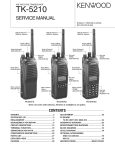
500-2 Service Manual
500-2
Service Manual
1
500-2 Service Manual
500-2 Service Manual
Contents
Chapter 1
Chapter 2
Chapter 3
Chapter 4
Chapter 5
Chapter 6
Chapter 7
Chapter 8
Chapter 9
Chapter 10
General
Radio Overview
Mode Introduction
Disassembly For Repair
Circuit Description
PCB Layout
Adjustment
Bill Of Materials
Charger
Block and Schematic
Appendix 1 Abbreviations
Appendix 2 Main Technical Indexes
Appendix 3 Trouble Shooting
2
500-2 Service Manual
Chapter 1 General
1.1 Introduction
This manual applies to the service and maintenance of 500-2 radios, and is for the
engineers and professional technicians that have been trained by our company. In this
manual you can find all the information of product service. Our company reserve the rights
to modify the product construction and specification without notice in order to enhance
product performance and quality.
Read this manual before repairing the product.
1.2 Attention
Safety
Do not touch the antenna connector with your skin directly. .
Do not reverse the power polarities.
Do not turn on the radio before the antenna and load connection is completed.
Do not contact the damaged antenna when transmitting, or may make lightly burning on the
skin.
Electromagnetism Interference
It’s prohibited to use or repair the radio in the following places:
Hospital, health center, air port
Any area with a potentially explosive atmosphere (e.g. fuel and chemical storage and
transport devices etc.)
Any area of dynamite or exploder.
Change Components
All the components used in repair service should be supplied by our company.
Other components of the same models available on the market are not surely able to use in
this product and we do not guarantee the quality of the product using such components.
1.3 Service
All the products of our company are subject to the service warranty.
After-sales service will be provided, and the length of warranty is stated by our company.
The radio and its accessories are all in the warranty. However, in one of the following cases,
charge free service will be not available.
No valid service warranty or original invoice.
Malfunction caused by disassemble, repair or reconstruct the radio by the users without
permission.
Wear and tear or any man-made sabotage such as mechanical damage, burning or water
3
500-2 Service Manual
leaking.
Product serial number has been damage or the product trademark is difficult to identify.
Beyond the warranty time, lifetime service is still available with paid. And we also provide
service components to service stations and staff.
4
500-2 Service Manual
Chapter 2 Radio Overview
1. PTT ( PUSH-TO-TALK) Button
To make a call, press and hold the PTT button, then speak into the microphone in
normal voice. Release the PTT button to receive signals.
2. Side Button 1 (Programmable Button)
3. Side Button 2(Programmable Button)
4. Channel Selector
Rotate to select channel 1~16.
5. Power/Volume Knob
Turn clockwise to switch on the radio.
Turn counterclockwise till a click is heard to switch off the radio.
Rotate to adjust the volume after turning on the radio.
6. LED Indicator
LED Indicates Status/Alert. Green LED lights when a carrier is detected in the current
channel. Red LED lights during transmission. Orange LED flashes when receiving the
Radio ID 5-Tone signaling or 2-Tone signaling or MDC signaling. Green LED flashes
when scanning. Red LED flashes when low battery.
7. Speaker/Microphone Jacks
Used to connect the optional speaker/microphone.
8. MIC Input
Please keep your mouth about 10 cm (3-4 inches) away from the microphone input
to achieve the best voice quality. If the distance is too far or too close to the radio, it
will affect the voice quality.
5
500-2 Service Manual
Programmable Button Function
The dealer can program the Side Button 1, Side Button 2 and the Top Button with the
following Optional functions:
None (No Function)
Annunciation Selection
Talkaround
Call1/Call2/Call3/Call4
Lone Work
Emergency Call
Cancel Emergency Call
Scan
Noise Channel Delete
Call Forward
H/M/L Power Switch
Squelch Adjust
Monitor Momentary/Call Cancel
Monitor/Call Cancel
Squelch Off Momentary/Call Cancel
Squelch Off/Call Cancel
Lock Keyboard
Battery Check
Surveillance
CTCSS Scan/Forever Save CH
CTCSS Scan/Save CH
6
500-2 Service Manual
Chapter 3
Mode Introduction
Mode combinations
Mode
User Mode
Data
Programming
mode
PC
Mode
Test Mode
Firmware
Upgrading
Mode
Function
For normal use
Reading and writing
frequency data and other
functions
Used to tune the radio
using the PC.
Upgrades the software
when new features are
added
How to access
Power on
Receive instructions from
the PC
Receive instructions from
the PC
Receive instructions from
the PC
User Mode:
You can enter User Mode (conventional communication mode) by turning on the power
switch. Users in the mode can use the defined function of the radio.
Data programming mode:
Before leaving the factory, the radio has been set in factory. However, due to different
requirements of users, functional parameters of the radio such as working frequency,
channels, CTCSS/DCS and auto scanning, etc. should be set again. Therefore, the
company has specially designed a set of 500 Programming software with friendly interface,
convenient operation and visualized display for setting functional parameters of the radio.
Steps for setting the functional parameters of the interphone by computer are as follows:
1. Install 500 Programming software on the computer.
2. As shown in the figure below, connect the radio to the computer through a special serial
or USB programming cable.
Computer
(RS232 serial port
/USB port)
Programming
cable
Figure 3-1
3. Turn on the power of the computer.
7
Radio
(Earphone /Program port)
500-2 Service Manual
4. Turn on the power of the interphone.
5. Click on 500 Programming software icon to perform the program.
6. In the main menu of the programming software, click on [Read] to read the parameters
of the radio into the computer; click on [Write] to write the parameters set in the
computer into the radio.
Caution:
1. Before editing for the first time, the data should be read from the interphone and
properly backed up.
2. If the edited data cannot work normally after being written into the interphone, please
open the backup data and rewrite them.
3. “Model Information” is the important information of the interphone and should not be
altered.
Test Mode
According to Figure 3-1, connect the radio to the computer with the special programming
cable.
Warning: Before entering the Test Mode, please first connect a high-frequency load of 50
ohm to the antenna port of the radio or connect the radio a certain test instrument.
With the 500 Programming Software, you can enter the adjustment status in Computer Test
Mode to adjust the following parameters of the radio:
(1) Frequency stability
(2) RF transmitting high power
(3) RF transmitting Middle power
(4) RF transmitting Low power
(5) Maximum TX voice deviation
(6) VOX1(Tight)
(7) VOX10
(8) 2/5 tone deviation
(9) DTMF deviation
(10) MSK deviation
(11) DCS/LTR balance
(12) DCS deviation
(13) LSD deviation
(14) CTCSS(67.0Hz) deviation
(15) CTCSS(254.1Hz) deviation
(16) Battery warning level
(17) RX Sensitivity
(18) DCS RX middle level
(19) RX squelch 9 open level
(20) RX squelch 9 close level
(21) RX squelch 1 open level
(22) RX squelch 1 close level
8
500-2 Service Manual
(23) RSSI(-120dBm)
(24) RSSI(-70dBm)
Firmware Upgrading Mode
The radio is equipped with an internal FLASH ROM, it can be upgraded if required.
1. Connect the radio to the PC with a proper programming cable, then power on the radio.
2. Run computer programming software.
3. Select the right “com port” you connected and the upgrading firmware and then click on
“E.P” to start downloading.
4. Turn off the radio and exit the programming software.
9
500-2 Service Manual
Chapter 4
Disassembly For Repair
The radio is a kind of sophisticated communication equipment with small and fine
mechanical structure. You should assemble and disassemble it carefully during the
maintenance process. The Instruction for assembly and disassembly are as follows:
Installing/Removing the Battery Pack
To install the battery, please place it into the groove on the top of the radio chassis about
5mm away from latch.
If the radio has the belt clip installed, you will have to press one side of the clip, to raise it
and slide the battery in proper position.
Press the battery with your fingers and push the battery until you hear a latch click, the
battery is now installed.
Removing the battery pack:
If you want to remove the battery from the radio, first press the battery latch located on the
bottom of the radio, and then press down to slide the battery about 5mm to release the
latch.
10
500-2 Service Manual
Notice:
* Do not short-circuit the battery terminals or dispose the battery in fire.
* Do not disassemble the battery case.
Installing/Removing Antenna, Channel Selector, Power/Volume Knob
Screw the antenna out of the connector at the top of the radio by holding the bottom of the
antenna and turn it counter clockwise until apart.
Using a smooth tool or a tool protected with cloth to hold or prize up form the bottom of
channel selector or volume knob until apart,then screw the two screws under the channel
selector and volume knob using the special tool.
11
500-2 Service Manual
Install external speaker/MIC
Open the cover of the jack for external speaker/MIC, and then insert the plug of the external
speaker or microphone into the jack on the radio. When inserting the accessory plug, make
sure it is properly aligned ( straight) to avoid internal damage to the connector in the radio.
12
500-2 Service Manual
Installing/Removing the Belt Clip
Use the 2 screws (M2.5x8.0) supplied with the radio and fix these screws on the holes in
the radio clip and into the holes in the aluminum case. If you want to remove the clip from
the radio, just unscrew them, and remove the clip, you can put the screws back to make
sure you do not loose them.
13
500-2 Service Manual
Installing/Removing the Chassis, PCB
14
500-2 Service Manual
1. Remove the antenna, channel selector and power/volume knob and two screws
under the channel selector and volume knob.
2. Screw off the two screws at the bottom of the radio by a hexagon screwdriver.
3. Pry up the aluminum shell by peaking a straight screwdriver in the cross-slot at the
bottom of the
aluminum shell, and then pull out the surface shell after placing the
aluminum shell inclined to the back;but please be careful not to snap off the cable of the
speaker.
4. Screw off the 11 screws on the PCB by a cross screwdriver.
5. Unsolder the endpoints of the antenna , PTT key board and speaker by an electric iron,
then remove the main board.
After the disassembly above, you can carry out corresponding reparation and debugging
according to the actual malfunction.
15
500-2 Service Manual
Exploded View of the Parts
16
500-2 Service Manual
No.
1
2
3
4
5
6
7
8
9
10
11
12
Parts No.
604CU50001001
2010CU600004X
2020CU500004X
304060250001X
2010CU600006X
304070250001X
2010CU600007X
7100500240471
2030CU600003X
2020CU500003X
2010CU600005X
2020CU500002X
Description
Cabinet asm.
Ear phone cabinet
O-ring Φ5X1.5
Volume screw M6X0.75X2.5 special shape brass
Volume knob black
Volume screw M7X0.75X2.5 special shape brass
Encoder knob black
Anntenna
SMA RF socket
O-ring Φ7X1.5
radio top cover black
2 PIN power socket washer
17
Qty.
1
1
2
1
1
1
1
1
1
1
1
1
500-2 Service Manual
13
14
15
16
17
18
19
20
301250607001X
7110CLP02001
70600CB03001
301200807001X
2030CU500001X
1010500200102
2020CU500001X
301200407001X
machine screw M2.5X6.0 PB(+) black Ni-plate
CLP-02 clip asm.
Battery CB-03 (OR CB-05 70600CB05001)
Machine screw M2.0X8.0
AL cabinet polishing ADC 12
Main PCB
cabinet waterproof ring
machine screw M2.0X4.0
2
1
1
2
1
1
1
14
Exchangeable part list
No.
1
2
3
4
5
6
7
8
9
10
11
12
Parts No.
604CU50001001
2010CU500001X
2010CU600010X
2010CU600002X
2010CU600003X
2010CU600008X
2020CU600001X
306003301001X
1211361601001
2040CU600004X
2020CU600004X
2010CU600009X
2030CU600004X
Description
Cabinet asm.
Radio front cabinet black
Light-guider clear PC
PTT plastic key black
Ear phone plastic plug
Ear phone cover black
PTT silicon key block
Φ36mm air filter nylon weave
Speaker Φ36mm
7mm mic air filter Φ7.0X4.5X0.2
Mic waterproof washer
Battery locker black
Spring Φ2.3X10.5 Φ0.25
1
1
1
1
1
1
1
1
1
1
1
2
1
2
3
4
5
604CU50001002
2030CU500001X
2010CU600005X
2020CU500001X
2020CU500002X
301250607001X
AL cabinet asm.
AL cabinet
Radio top cover black
Cabinet waterproof ring orange
Power socket washer
Machine screw M2.5X6.0
1
1
1
1
2
2010CU600006X Volume knob
2010CU600007X Encoder knob
7110CLP02001
CLP-02 Clip
18
Qty.
500-2 Service Manual
Chapter 5
Circuit Description
5.1 Frequency configuration
The reference frequency of frequency synthesizer is provided by 12.8MHz crystal oscillator
X1 TCXO. The receiver adopts quadric mixing mode. The first IF is 38.85MHz, and the
second IF is 450kHz. The first local oscillation signal of the receiver is produced by
frequency synthesizer and the second local oscillation signal selects the 3rd harmonics of
12.8MHz of crystal oscillator X1 TCXO. The signal of transmitter is produced by frequency
synthesizer directly.
Figure 5. 1 Frequency configuration
5.2 Receiver(Rx)
The receiver is double conversion superheterodyne, designed to operate in the frequency
range of 400 to 470MHz,The frequency configuration in Fig 2
19
500-2 Service Manual
Figure 5.2 Receiver section configuration
Front End of Receiver
Signals from the antenna are filtered by BPF which consists of C235 C236 C233 C604
C252 C951 C234 C255 C260 L211 L209 L208 D201 D202 and D204 via RX/TX switch
(D101 D102 and D103). After being filtered out the useless out-of-band signals, the
signals are amplified by LNA consisting of Q203 and external components.
Signals from LNA are filtered again by BPF which consists of C228 C226 C238 C229 C227
C239 C947 C259 C948 L214 L204 L203 D905 D206 and D206 before entering the 1st
mixer (Q202).
The PWM wave is output by MCU composed of 58 foot and then commutated to adjustable
voltage after filtering to change the capacity of varactor diode D905 D203 D206 D201 D202
and D204 to control the center frequency of BPF.
1st mixer
The first IF (51.65MHz) signal is produced after mixing of the receiving signal from LNA and
the 1st local oscillation signal from frequency synthesizer. The first IF signal is filtered out
adjacent channel and other useless signals by crystal filter (XF201).
IF Circuit
The 1st IF signal from crystal filter is amplified by the first IF amplifier (Q201) before
processing of IC in IF( IC200,GT3136).
IF IC consists of the 2nd mixer, 2nd local oscillation, IF amplifier, limiter, frequency
discriminator and noise amplifier.
Frequency (12.8MHz) produced by TCXO(X1) is amplified and then selects 3rd harmonics
(38.4MHZ) as the second local oscillator signal source. The second IF signals (450kHz) are
generated after signals mixing of the second local oscillation (38.4MHz) and the first IF
(38.85MHz) in IC200. Audio signals are demodulated and outputted by IC200 after the
second IF signals are amplified and limited in IC200 and then filtered by ceramic
filter(450kHz).
20
500-2 Service Manual
Figure 5.3 Schematic Diagram for IF System
Receiving Audio Signal Processing:
The audio processing circuit of receiver consists of IC300 and the peripheral circuit. Voice
signals from IC200 are sent to IC301(CTCSS signaling filter circuit)and IC300-D
respectively after amplified in IC300-C. After that, the signals are removed of the HF and LF
components after amplification, de-emphasis and filtering by other units of IC300, and only
audit components from 300 to 3000Hz can be sent to audio power amplifier (IC302) after
amplified in Q300 and adjusted by volume potentiometers.
Figure 5.4 Schematic Diagram for Audio Processing of Receiver
21
500-2 Service Manual
Squelch Circuit
Part of the AF signal from the IC200 enters the FM IC again,and the noise component is
amplified and rectified by a filter and an amplifier to produce a DC voltage corresponding to
the noise level.
The DC signal from the FM IC goes to the analog port of the microprocessor(IC403).IC403
determines whether to output sounds from the speaker by checking whether the input
voltage is higher or lower than the preset value.
To output sounds from the speaker,IC403 sends a high signal to the MUTE and AFCO lines
and turns IC302 on through Q302 Q304 and Q305.
Audio Power Amplification
The audio power amplifying circuit consists of IC302 and the peripheral components.
The signals are amplified by audio power amplifier to drive the speaker after collecting the
receiving audio signals, voice signals and warning tone signals. The warning tone has no
volume limitation.
When AFCO is high level, Q304 is on, IC302 begins to work and the speaker sounds.
Speaker Impedance: 16ohm
CTCSS Signal filtering
The audio signals after demodulation in IC200 may contain CTCSS (continuous tone
control squelch system) or DCS(digital squelch)signals. The spectrum component of
CTCSS/DCS is 67 to 250Hz. The filtering circuit composed of IC301 can filter out signals
except CTCSS/DCS spectrum, which makes MCU decode the CTCSS/DCS more
accurately.
5.3 Transmitter (Tx)
Transmitter Power Amplifier
Figure 5.5 Schematic Diagram for Power Amplifier and Antenna Switch
22
500-2 Service Manual
The modulated RF signals from VCO are amplified by Q101, Q102 and Q105 before the
power amplification in Q107.
Gate bias of Q105 and Q107 is controlled by APC circuit, so the output power of transmitter
can be controlled conveniently by changing the gate bias voltage.
APC(Automatic Power Control)
Figure 5.6 Schematic Diagram for APC Circuit
R130 R131 and R132 are power amplification current detector, IC100A is power
amplification current sampling amplifier and IC00B is power comparison amplifier.
The power amplification current and IC100A output will increase with oversized output
power of transmitter. When the output voltage of IC100B decreases, the bias voltage of
Q105 and Q107 will decrease, finally the output power of transmitter will decrease or vice
versa. Thus, the output power of transmitter will keep stable under any different working
condition.
MCU can set the power by changing the voltage input to IC100B.
Audio Signal Processing of Transmitter
Figure 5.7 Schematic Diagram for Audit Circuit of Receiver
23
500-2 Service Manual
The audio signal processing circuit of Transmitter consists of IC500 and the peripheral
components. Voice signals from MIC are sent to VCO for modulation together with
CTCSS/DCS after amplification, limitation and filtering.
AGC circuit consists of D500, D501 and Q503. The signal amplitude is reduced to ensure
no distortion in case of oversized MIC signal.
Q504, the power switch of voice processing circuit, controlled by MCU, will give power
supply to IC500 only during transmission.
J501 is the socket for external MIC, and the internal MIC will disconnect automatically when
using external MIC, but the internal PTT is still effective.
5.4 PLL Frequency Synthesizer
Figure 5.8 Schematic Diagram for Frequency Synthesizer
The 500-2 adopts PLL frequency synthesizer.
Frequency synthesizer consists of reference oscillator, voltage controlled oscillator (VCO),
programmable frequency divider (PFD), phase comparator and low pass filter (LPF).
RX VCO Unit consists of Q4 D2 D4 L14 C35 C41 C44 C45 and D1 Q5.
TX VCO Unit consists of Q4 D2 D4 L14 C35 C41 C44 and C45,D5 is the modulation circuit
of VCO.
IC1 (MB15E03) is PLL integrated circuit and contains programmable parametric frequency
divider (PPFD), programmable frequency divider (PFD), phase comparator and charge
pump, etc.
Low pass filter consists of R5 R7 R9 R10 C12 C15 and C18.
Reference frequency is provided by X1 (TCXO, 12.8MHz).
Reference frequency of TCXO (Temperature-controlled Crystal Oscillator) is divided by
PPFD in IC1 to produce reference frequency of 5kHz or 6.25kHz (controlled by MCU based
on the set channel frequency).
24
500-2 Service Manual
The oscillation frequency of VCO is compared with reference frequency to produce error
signal after divided by PFD in IC1. The error signal is filtered by low pass filter before
changing the VCO frequency to the set value in VCO (it is locking).
N=FVCO/FR
N:Division Frequency
FVCO:VCO Oscillation Frequency
FR:Reference Frequency
Lock lost detection: When PLL is out of lock, IC pin14 will output low level signal to MCU,
and then MCU prohibit transmitter from transmitting with a warning tone.
Q8, the power filter, can provide PLL with more purified power to reduce the noise of
frequency synthesizer.
5.5 Voice Circuit
The station is equipped with Voice Prompt Function, which is very useful during night or
under dark condition.
The speaker will voice the current channel number when changing the channel every time
because of the voice memory chip (IC401), which stores channel voice prompts.
5.6 Power Supply:
The station use lithium battery (7.4V, 1300mAh), while transmitter amplifier circuit (Q105
Q107) and receiver audio amplifier (IC302) use battery directly for power supply, and other
circuits use regulated voltage (5V and 3V).
IC404:micro-power voltage stabilizer of 3V LDO, provides power (3V) of heavy current for
the station together with Q10 and Q30.
IC902:5V LDO
Q405: 5T switch (controlled by MCU)
5T: supply power for the front end of transmitter
Q408: 5R switch (controlled by MCU)
5R: supply power for the units such as RF amplification, mixing, IF processing and
audio signal processing.
Q910: 5C switch (controlled by MCU)
5C: the power (5V), controlled by power-down mode, is the supply power of
frequency synthesizer.
25
500-2 Service Manual
5.7 MCU Unit:
5.9 Schematic Diagram for MCU Unit
MCU Unit controls the operation of every unit to realize all functions of the 500-2
Communication with external PC
State data access
Control PLL for the generation, receiving and transmitting of local oscillation frequency
Access to the current channel state
Control LED status indicator
Control power supplied condition of every unit
Detect action of every function key
Produce CTCSS signal
Produce DCS signal
Produce power controlled signal
Finish CTCSS decoding
Finish DCS decoding
Squelch detection and control
Control voice prompt content
Memory (FLASH)
Channel data, voice data and other function setting data and parameter adjustment data.
26
500-2 Service Manual
CTCSS/DCS signal coding and decoding:
CTCSS/DCS signals from MCU (pin22 and pin18 output) are sent to VCO and TCXO for
modulation respectively after filtering by R500 R501 C500 C501 and R504 R503 C920
C921.
CTCSS/DCS signals from receiver are sent to MCU(pin52) for decoding, and then MCU
test if there are CTCSS/DCS signals with the same setting of the station to decide
whether open the speaker or not.
CTCSS (continuous tone control squelch system, hereinafter referred to as CTCSS), is a
kind of squelch control system with modulation on carrier and continuous sub-audio signals
as pilot tone. If CTCSS function is set, the call is available only at the same CTCSS
frequency of both receiving and transmitting parties to avoid the disturbance of other
signals.
The station has 39 groups of standard CTCSS frequency for your selection, such as Table
5.1.
CTCSS signals produced by MCU are sent to VCO for modulation after filtered the HF
components over 300Hz in low pass filter composed by RC.
27
500-2 Service Manual
Table 5.1
No.
1
2
3
4
5
6
7
8
9
10
CTCSS Frequency Table
Frequency
[Hz]
67.0
69.3
71.9
74.4
77.0
79.7
82.5
85.4
88.5
91.5
No.
11
12
13
14
15
16
17
18
19
20
Frequency
[Hz]
94.8
97.4
100.0
103.5
107.2
110.9
114.8
118.8
123.0
127.3
No.
21
22
23
24
25
26
27
28
29
30
Frequency
[Hz]
131.8
136.5
141.3
146.2
151.4
156.7
162.2
167.9
173.8
179.9
No.
31
32
33
34
35
36
37
38
39
Frequency
[Hz]
186.2
192.8
203.5
210.7
218.1
225.7
233.6
241.8
250.3
DCS signaling:
DCS (Digital code squelch), is a kind of continuous digital code modulated on carrier with
voice signal and used for squelch control. If DCS function is set, the speaker is available
only when receiving the same DCS code to avoid the disturbance of useless signals.
The station has 83 kinds of standard codes including positive and inverse code for your
selection, such as Table 2.
DCS signals produced by MCU (PWM waveform) are sent to VCO and TCXO for
modulation (the HF components of DCS signals are modulated by VCO, while the LF
components by TCXO) after filtered the HF components over 300Hz in low pass filter
composed by RC.
CTCSS/DCS signals from receiver are sent to MCU for decoding, and then MCU test if
there are DCS codes with the same setting of the station to decide whether open the
speaker or not.
28
500-2 Service Manual
Table 5.2
DCS Coding Schedule
023
025
026
031
032
043
047
051
054
065
071
072
073
074
114
115
116
125
131
132
134
143
152
155
156
162
165
172
174
205
223
226
243
244
245
251
261
263
265
271
306
311
315
331
343
346
351
364
365
371
411
412
413
423
431
432
445
464
465
466
503
506
516
532
546
565
606
612
624
627
631
632
654
662
664
703
712
723
731
732
734
743
754
5.8 Description of Semiconductor Devices
The distribution of each pin goes as the table 5.3.
Table 5.3---Definition of CPU Base Pin:
Pin No.
Port Name
1
2
APCSW
PTT
3
MODE
Pin
Name
P33
P34
-
O
I
Active
Level
H
L
-
-
I/O
29
Function
APC switch
PTT switch input
Connect this pin to VCC via a 4.7K
resistor(*Burn)
500-2 Service Manual
4
5
6
7
8
9
10
11
12
13
14
15
16
17
18
19
20
21
22
23
24
25
26
27
28
29
30
31
SK1
SK2
RESET
XOUT
VSS
XIN
VCC
BSHIFT
F_CS
F_DI
F_CLK
F_DIO
NC
VCCN
DCSTCXO
PLL_CLK
PLL_DAT
PLL_EN
DCSVCO
PLL_UL
RXVCO
BEEP_AF
RXD0
TXD0
GLED
RLED
NC
TDIN
P43
P44
P54
P53
P52
P51
P50
P27
P26
P25
P24
P23
P22
P21
P20
P17
P16
P15
P14
P86
P85
P84
P83
I
I
I
O
I
O
O
O
O
I/O
O
O
O
O
O
O
O
I
O
O
I
O
O
O
O
I
L
L
L
H
L
H
H
H
H
H
H
TRFI
32
ALARMC
P82
O
L
33
34
35
36
37
38
39
40
41
42
DEV2
DEV1
NARROW
MIDDLE
TXD1
RXD1
MIC_MUTE
5TC
EXTPTT
SAVE
P81
P80
P60
P45
P66
P67
P65
P64
P63
P31
O
O
O
O
O
I
O
O
I
O
H
H
L
H
L
H
30
SIDE KEY1 input
SIDE KEY2 input
CUP reset (*Burn)
MCU clock
GND
MCU clock
+3V
Beat shift switch
FLASH chip select output
FLASH data in
FLASH serial clock output
FLASH data input/output
Frequency regulation output(PWM)
CTCSS/DCS output(PWM)
PLL clock Output
PLL data Output
PLL enable
CTCSS/DCS output(PWM)
PLL unlock detect pin
TX/RX VCO selection(H,RX)
Local Beep Control Pin
Serial data
Serial data
Green LED
Red LED
TONE data input
Alarm switch control(H:Controlled by
Volume Switch
L:Emergency siren maximum volume)
Voice deviation adjustment 2
Voice deviation adjustment 1
12.5KHz
20KHz
Reserved
Reserved
MIC mute
L: MIC mute
Transmitting power control
External PTT switch input
Battery power control H:Power save
500-2 Service Manual
43
44
45
46
47
48
49
50
51
52
53
54
55
56
57
58
59
60
61
62
63
64
5RC
ENC0
ENC1
ENC2
ENC3
VOX
BATT
AFCO
SPKSW
DCS_IN
NC
BUSY
TOPKEY
RXMUTE
RSSI
PCTV
AVSS
DTMF
VREF
AVCC
NC
RX_W/N
P30
P36
P32
P13
P12
P11
P10
P00
P01
P02
P03
P04
P62
P61
P05
P06
P07
P37
P53
O
I
I
I
I
I
I
O
O
I
I
I
I
O
I
O
I
O
I
I
O
O
H
AN9
AN8
L
L
AN5
Receiving power control
Channel selector input
Channel selector input
Channel selector input
Channel selector input
VOX level input
Battery voltage input
Audio Amplification Power
Audio amplifier control
CTCSS/DCS input Recording level input
AN3
L
H
AN2
DA0
Busy level input
TOPKEY input
RX audio mute
Received Signal Strength Indicator input
APC/BPF control output
GND
DTMF/Beep output
+3V
+3V
DA1
H
RX Wide/Narrow switch
Table 5.4 Functional description of semiconductor device
Item
IC1
IC100
IC200
Model
MB15E03
NJM2904
GT3136
IC300 NJM2902V
IC500 NJM2100V
IC302 TDA2822D
Function Description
Frequency Synthesizer
APC, Voltage Comparison, Driving
Receiver 2nd Local Oscillation, 2nd IF Amplification,
Limitation, Demodulation, Noise Amplification
Receiver demodulated signal Amplification, Filtering
MIC Amplification, Limitation, Filtering
Audio Frequency Power Amplification
IC401 W25Q80
FLASH, Channel Frequency Data Storage, Function
Setting Parameter, Debug Mode Parameter
IC403 R5F212BCSNFP MCU
31
500-2 Service Manual
Chapter 6
500-2 PCB Layout
32
C330
R923
C332
D401
R417
D402
D400
S404
R327
ANT
C334
R536
R334
C333
R335
R133
IC100
R135
C336
C963
SP
R332
R141 R138
R134
C335
R959
Q307
C132
C337
C331
C134
R136
Cy1
Q306
C530
Cy2
R137
R333
R336
IC302
C931
R962
C962
L118
C531
C533
R140
R142
C970
Cy3
R535
R146
R958
L500
Q109
C519
C524
R533
C521
R529
C526
R144
R526
C967
D903
Q106
R969
D501
Q914
R530
C935
C518
C903
C522
R525
R341
R548
C520
R528
C525
IC500
Q903
C969
Q503
R532 R968
R527 C924
K1
Q902
R534
D500
C940
Q912
Q300
C514
R520
C512
Q502
R519
R512
C982
R543
R508
R507
R925
TH501
R961
R964
C502
C920
R502
R504
C338
R416
C500
C929
C930
C415
IC400
R412
L403
C409
C412
Q403
R501
C408
R929
C400
Cy6
R513 C501
R927
R607
R409
R400
R500
C504
R928
C706
1
C413
L402
C925
L400
TH201
C403
C916 C915
C937
R921
C917
R920 R919
R918
R922
R901
R207
R910
C914
R413
R911
C908
R917
C913
R963
R955
R909
R916
C910
R912
C911 C909
IC901
R913
R914
C912
R915
IC403
IC401
X400
C936
C960
R318 C961
Q913
R401
C418
C921
C425
R414
R965
R423
C319
C926
R505
C410
C943
R541
Cy5
R503 R983
C505
R967
C308
C411
R506
R407
C710
R408
R316
R325
C314
Q908
R510
C535
C927
R313
R421 C422
R323
C510
Q907
C928
R411
C419
C318
Q501
VR501
C310
R415 C420
IC301
R320
R514
C503
R305
C304
C515
C301 R303
C315
R306
R301
C313
R311
C303
C300 R302
R304
R338
C906
R511
C506
C513
C511
C508
C306
Q901
C509 R515
R317
R315
IC300
Q500
R517
C534
R908
R522
R521
C309
R307
R308
R516
C305
C307
C923
R524 C934
R523
R314 C312 R312
R322
R418
MIC500
C302
C316
Cx3
R309
R300
R340
C321
R324
R321
R984
R328
C320
R326
C322
R972
Q302
C904
Q504
C516 C517
R973
R537
R145
C527
C141
C139
C529
Q108
R403
C402
R410
Q400
R426
R339 C406
Q401
R402
S401
C154
C327
C149
C147
Cx4
C150
L109
R132
L112
C126
C148
C131
C136
L107
C128
D101
C129
C138
R131
R130
L501
C528
R139
C155
L113
R154
J500
L114
C151
C964
C143
Q304
C932
R330
R331 Cx19
C153
Q305
L502
VR401
C145
C142
C130
C125
L110
L106
C170
J502
J501
C135
D102
C140
D103
C144
R147
C235
L211
C23
C602
C127
C260
C232
C231
R220
R601
C949 R223
L206
C237
Cx18
Cx17 C939
C226
D203
D206
XF201
C215
C902
C905
C223
R210 C214
C212
R208
Q201
R209
Cx23
C201
IC200
C208
R203
C204
C213
C202
C203
Q200
C210
R204
R202
C205
R201
C256
C211
C207
IC2
C233
R128
R127
L103
R109
C606 C938
C217
Q303
R205
C603
C238
C965
L200
R212
R211 C221
R329
R11
C57
L214
C239
C51
C200
C58
C30
C6
R35
C416
IC404
C417
C3
C414
C610
C2
R952
L204
C947
R215
C209
R12
L17
C26
C922
R932
Cx24
X1
R951
C229
L16
C206 R206
R2
C16
C28
Q1
D7
IC1
R950
C227
R8
C19
C14
L213
L4
C9
C7
L1
C601
R6
R1
D905
CF201
R4
C10
C609
L6
L5
L2
C25
C29
R9
R10
R7
R5
C1
R14
C20
C257
L904
C17
R3
C27
C957
C224
C220 R216 R603
R605
Q202
C228
L203
C107
L101
R604
C218
C241
L202
R226
R105
C219
Cx10
C4
R218
L207
R219 C948
R200
R20
C5
Cx2
C54
Cx9
Q2
R13
C12
R21
C15
C18
L7
R108 C108
R115
C222
D200
D100
L100
R103
Cx11
C24
R19
R18
Cx8
R214
L201
R15
C110
C114
Q101
R110
C607
R222
C708
C157
R107
Cx16
Cx14
C56
C156
R106
Cx15
D907
D4
C35
R102
Q203
R221
R228
C105
R16
C36
L10
C104
C102
Cx5
L18
C53
L21
Q100
C101
L11
R706
R112
C111
C103
R100
L9
D908
D2
R101
C100
R27
C31
D5
L14
C950
R104
Q6
TC1
R32
R31
C49
L902
C39
C41
C106
L212
R111
L102
R113
C951
L208
C956
R34
D1
C45
R30
C38
C44
C40
Q8
Q5
Cx6
L901
R33
Q4
R22
L19
C42
C918
D6
C48
R26
C52
C55
C43
C46
C252
C253 R230
C109
Q102
C234
R231
D201
R121
R120
L209
C255
C259
Q105
C958
R602 C604
C430
R125
R429
L119
Cx22
D202
C121
C532
C123
R126
C118
Q408
Q406A
C254 R232
Cx1
L104
R118
IC902
Q407
R117
C959
C424
R433
C119
C429
R428
Cx13
C116
C407
D204
Q911
Q406B
R425
R427
Q405
C966
C113
Q404
C37
C423
R422
L105
R420
Cx21
C421
Q107
R424
R432
R419
C236
Q910
Cx20
C120
R435
R434
C261
C427
CD200
500-2 Service Manual
Chapter 7
ADJUSTMENT
7.1 Required Test Equipment
Table 7.1
Number
1
2
3
4
5
6
7
8
9
10
11
12
13
14
Name
Computer
Programming
software
Programming
cable
Dubbing cable
DC regulator
Parameter requirements
Above P2, compatible IBM PC, WINDOWS
98/ME/2000/XPOperating System
500 Programming software
Special Serial/USB (CPL-01) programming cable
CPL-02
Output voltage:7.5V, output electric current:≥ 5A
Test range: 0.5---10W
Frequency range: 100MHz—500MHz
RF power meter
Resistance: 50Ω
SWR≤1.2
Frequency range: 0.1—600MHz
Frequency
Frequency accuracy: higher than±1×10⁻⁶
meter
Sensitivity: higher than 100mV
Frequency
Frequency range: DC—600MHz
deviator
Test range: 0--±5kHz
Input resistance: above 10MΩ/V DC, capable of
DMM
measuring voltage, electric current and resistance.
Audio signal
Frequency range:2---3000Hz
generator
Output level: 1---500mV
RF power
Decrement: 40db or 50db
attenuator
Receive power : higher than10W
Standard signal Frequency range:10MHz---1000MHz
source
Output level:0.1uV~32mV (-127dBm~-17dBm)
Frequency range: DC~20MHz
Oscilloscope
Test range: 10mV~20V
Audio
Frequency
Test range: 10mV~10V
voltmeter
Recommend how to use: item 6, 7, 8, 10, 11 and 12 which listed in the table can be
substituted by integrated tester HP8920/HP8921.
33
500-2 Service Manual
Figure 7.1 External Speaker/microphone
Interface Definition
7.2 Adjustment Items
Some detection and adjustment shall be made to the station technical data after changing
the components during the maintenance. The debugging introduction of some related
circuits goes as follows:
Some parameters of the product can be adjusted by use of 500 Programming Software of
our company. The adjustable parameters are as follows:
(1) Frequency stability
(2) RF transmitting high power
(3) RF transmitting Middle power
(4) RF transmitting Low power
(5) Maximum TX voice deviation
(6) VOX1(Tight)
(7) VOX10
(8) 2/5 tone deviation
(9) DTMF deviation
(10) MSK deviation
(11) DCS/LTR balance
(12) DCS deviation
(13) LSD deviation
(14) CTCSS(67.0Hz) deviation
(15) CTCSS(254.1Hz) deviation
(16) Battery warning level
(17) RX Sensitivity
(18) DCS RX middle level
(19) RX squelch 9 open level
(20) RX squelch 9 close level
(21) RX squelch 1 open level
(22) RX squelch 1 close level
(23) RSSI(-120dBm)
(24) RSSI(-70dBm)
34
500-2 Service Manual
Steps for adjustment:
1) Enter Computer Test Mode by selecting “Test Mode” in main menu of 500 Programming
Software.
2) Select the items to be adjusted in choice menus, and then adjust the parameters by
function keys on the computer keyboard.
3) Exit Computer Test Mode after adjustment.
7.3 Adjustment
7.3.1 VCO Adjustment
Close “Power-saving Mode”. Set receiving frequency to low frequency point (see Table 7.2)
and in the receiving state, test voltage of PD by DMM and adjust fine-tuning capacitor
TC1/TC2 to get CV voltage of 1.0V±0.2V
Set transmitting frequency to high frequency point (refer to Table 7.2), press PTT and test
voltage of PD by DMM, which shall less than 4.0V
Table 7.2 High/ Intermediate/ Low Frequency Point of All Models
Low Frequency
Point
500-2
7.3.2
400.100 MHz
Intermediate
Frequency
Point
435.100 MHz
High Frequency
Point
469.975 MHz
Frequency stability
Double-click to enter “Frequency Stability” in “Test Mode Manual” to achieve the rated
transmitting frequency by adjusting the number from 0 to 255 (Error<100Hz).
7.3.3
RF transmitting power
High power
Adjusts the transmitting power to 3.8-4.2W in the computer
(5 frequency points including Highest, High, Med, Low, lowest)
Middle Power
Adjust the transmitting power to 1.8-2.2W in the computer
Low Power
Adjust the transmitting power to 0.8-1.2W in the computer
7.3.4
Voice deviation
Maximum voice deviation
Signal source: MOD:1kHz/120mV LPF:15kHz
Adjust the max frequency deviation in the computer adjustment mode.
35
500-2 Service Manual
mode.
3.9kHz---4.5kHz (wideband)
3.2kHz---3.9kHz (median band)
between 1.8kHz---2.3kHz (narrowband)
(2/5)TONE, DTMF, MSK Deviation
Adjust TONE, DTMF, MSK deviation in the computer adjustment mode.
3.2---4.0 kHz (wideband)
3.0kHz---3.6kHz (median band)
1.8---2.3kHz (narrowband)
VOX1, VOX10
Adjust VOX1, VOX10 microphone sensitivity in the computer adjustment mode.
VOX1 for 50mv and VOX10 for 5 mv
7.3.5 CTCSS/DCS deviation
DCS/LTR balance
Signal source: LPF: 300Hz
Adjust DCS/LTR balance in the computer adjustment mode.
Make the transmitting demodulation waveform be flat square wave.
DCS deviation
Signal source: LPF: 300Hz
Adjust DCS frequency deviation in the computer adjustment mode.
0.50kHz---0.85kHz (wideband)
0.50kHz ---0.65kHz (medium band)
0.25kHz--0.45kHz (narrowband)
The waveform shall be good.
LSD deviation
Reserved for the future.
CTCSS(67.0, 254.1Hz) deviation
Signal source: LPF:300Hz
Adjust CTCSS deviation in the computer adjustment mode.
0.50kHz---0.85kHz (wideband)
0.50kHz ---0.65kHz (medium band)
0.25kHz--0.45kHz (narrowband)
The waveform shall be good.
7.3.6 Battery warning level
Adjust the battery warning level in the computer adjustment mode.
Set the power supply voltage at 6.8V, and press start and then end.
7.3.7 Receive sensitivity
36
500-2 Service Manual
Adjust the sensitivity in the computer adjustment mode.
Make the sensitivity of all frequency points the highest
(provided the sensitivity is the highest, the better data)
7.3.8 Squelch adjustment
Adjust squelch in the computer adjustment mode.
Squelch 9 open
The signal level output is set to -118dBm (wideband) or -117dBm (narrowband)
Automatically records the corresponding squelch level.
Squelch 9 close
The signal level output is set to -120dBm(wideband) or -119dBm (narrowband)
Automatically records the corresponding squelch level.
Squelch 1 open
The signal level output is set to -124dBm (wideband) or -123dBm (narrowband)
Automatically records the corresponding squelch level
Squelch 1 close
The signal level output is set to -126dBm (wideband) or -125dBm (narrowband)
Automatically records the corresponding squelch level
7.3.9 RSSI adjustment
RSSI(-120dBm), RSSI(-70dBm)
The signal level output is set to -120dBm or -70dBm.
Automatically records the corresponding RSSI level.
Note: Voltage for the aforesaid tests: 7.5V +/-0.1V in room temperature
37
500-2 Service Manual
Chapter 8
500-2
500-2 BOM
No.
PARTS LIST
Ver
Component
No.
Parts No.
Description
Name/Specificatio
n
Qt
TP-5002
01C
Ref. No.
y.
1
2
3
702CU5002001
4
701CU5002001
5
605CU5000201
6
71200CT02001
CT-02 radio ring
1
7
70700CP02001
CP-02 rapid charger
1
8
7100500240471
500-2 UNIT
500-2 portable
1
two-way radio
500-2 packaging
1
BOM
CU500U1 ANTENNA
(about 160mm)
CRAK435001010
400-470MHz
1
9
10
709CA02US001
11
70600CB05001
Power Supply(DC
12V 500mA)
Lithium-ion Battery
1300mAH 7.4V
CA-02
1
CB-05
1
12
13
14
701CU5002001
500-2 portable
two-way radio
15
16
RESISTOR
R4 R7 R13 R419 R901
17
1090400050001
0402 CHIP R 0Ω
RC0402JR-070R
6
18
1090410150001
0402 CHIP R 100Ω
RC0402JR-07100R
5
19
1090415150001
0402 CHIP R 150Ω
RC0402JR-07150R
1
R27
20
1090433150001
0402 CHIP R 330Ω
RC0402JR-07330R
2
R108 R113
21
1090456150001
0402 CHIP R 560Ω
RC0402JR-07560R
1
R5
22
1090468150001
0402 CHIP R 680Ω
RC0402JR-07680R
1
R110
23
1090482150001
0402 CHIP R 820Ω
RC0402JR-07820R
2
R429 R532
R911
R19 R26 R210 R211
R530
R2 R9 R10 R222 R328
24
1090410250001
0402 CHIP R 1kΩ
RC0402JR-071K
16
R407 R409 R413 R420
R427 R433 R434 R932
R951 R952 R967
25
1090415250001
0402 CHIP R 1.5kΩ
RC0402JR-071K5
38
4
R112 R331 R521 R525
500-2 Service Manual
26
1090418250001
0402 CHIP R 1.8kΩ
RC0402JR-071K8
4
27
1090422250001
0402 CHIP R 2.2kΩ
RC0402JR-072K2
5
28
1090427250001
0402 CHIP R 2.7kΩ
RC0402JR-072K7
2
R205 R329 R522 R908
R1 R226 R418 R536
R537
R422 R428
R100 R103 R105 R106
29
1090433250001
0402 CHIP R 3.3kΩ
RC0402JR-073K3
11
R203 R204 R303 R424
R425 R510 R548
30
1090439250001
0402 CHIP R 3.9kΩ
RC0402JR-073K9
1
R201
31
1090447250001
0402 CHIP R 4.7kΩ
RC0402JR-074K7
4
R32 R416 R607 R909
32
1090456250001
0402 CHIP R 5.6kΩ
RC0402JR-075K6
8
33
1090468250001
0402 CHIP R 6.8kΩ
RC0402JR-076K8
2
R523 R972
34
1090482250001
0402 CHIP R 8.2kΩ
RC0402JR-078K2
3
R339 R410 R426
R101 R301 R302 R324
R326 R910 R914 R923
R15 R33 R140 R308
35
1090410350001
0402 CHIP R 10kΩ
RC0402JR-0710K
16
R327 R432 R435 R501
R502 R503 R511 R516
R913 R920 R928 R964
36
1090412350001
0402 CHIP R 12kΩ
RC0402JR-0712K
2
R117 R312
37
1090415350001
0402 CHIP R 15kΩ
RC0402JR-0715K
3
R526 R527 R955
38
1090418350001
0402 CHIP R 18kΩ
RC0402JR-0718K
3
R305 R529 R919
39
1090422350001
0402 CHIP R 22kΩ
RC0402JR-0722K
7
40
1090433350001
0402 CHIP R 33kΩ
RC0402JR-0733K
8
41
1090439350001
0402 CHIP R 39kΩ
RC0402JR-0739K
2
R321 R500 R504 R506
R925 R927 R958
R508 R513 R514 R515
R519 R520 R929 R963
R313 R915
R22 R107 R118 R126
42
1090447350001
0402 CHIP R 47kΩ
RC0402JR-0747K
11
R141 R307 R320 R330
R917 R921 R968
43
1090451350001
0402 CHIP R 51kΩ
RC0402JR-0751K
1
R524
44
1090456350001
0402 CHIP R 56kΩ
RC0402JR-0756K
2
R216 R605
45
1090468350001
0402 CHIP R 68kΩ
RC0402JR-0768K
1
R602
46
1090482350001
0402 CHIP R 82kΩ
RC0402JR-0782K
3
R11 R543 R918
47
1090491350001
0402 CHIP R 91kΩ
RC0402JR-0791K
1
R300
R6 R21 R146 R221 R318
48
1090410450001
0402 CHIP R 100kΩ
RC0402JR-07100K
14
R323 R325 R341 R401
R408 R533 R541 R603
R961
49
1090412450001
0402 CHIP R 120kΩ
RC0402JR-07120K
2
50
1090415420001
0402 CHIP R 150kΩ
RC0402DR-07150K
6
51
1090418450001
0402 CHIP R 180kΩ
RC0402JR-07180K
2
52
1090422450001
0402 CHIP R 220kΩ
RC0402JR-07220K
6
39
R30 R340
R134 R135 R136 R137
R138 R507
R202 R306
R322 R411 R414 R415
R421 R423
500-2 Service Manual
53
1090427450001
0402 CHIP R 270kΩ
RC0402JR-07270K
4
R16 R18 R316 R317
54
1090433450001
0402 CHIP R 330kΩ
RC0402JR-07330K
2
R8 R400
55
1090439450001
0402 CHIP R 390kΩ
RC0402JR-07390K
1
R315
56
1090447450001
0402 CHIP R 470kΩ
RC0402JR-07470K
6
57
1090468450001
0402 CHIP R 680kΩ
RC0402JR-07680K
3
R208 R912 R922
58
1090475450001
0402 CHIP R 750kΩ
RC0402JR-07750K
2
R505 R528
59
1090410550001
0402 CHIP R 1MΩ
RC0402JR-071M0
7
60
1090418550001
0402 CHIP R 1.8MΩ
RC0402JR-071M8
1
62
1090600050001
0603 CHIP R 0Ω
RC0603JR-070R
5
63
109064R750001
0603 CHIP R 4.7Ω
RC0603JR-074R7
2
64
1090610050001
0603 CHIP R 10Ω
RC0603JR-0710R
7
65
1090622050001
0603 CHIP R 22Ω
RC0603JR-0722R
3
R109 R111 R218
66
1090647050001
0603 CHIP R 47Ω
RC0603JR-0747R
4
R121 R128 R212 R220
67
1090610150001
0603 CHIP R 100Ω
RC0603JR-07100R
3
R14 R31 R403
68
1090622150001
0603 CHIP R 220Ω
RC0603JR-07220R
2
R215 R402
69
1090627150001
0603 CHIP R 270Ω
RC0603JR-07270R
3
R102 R139 R154
70
1090647150001
0603 CHIP R 470Ω
RC0603JR-07470R
2
R535 R969
71
1090656150001
0603 CHIP R 560Ω
RC0603JR-07560R
1
R20
72
1090618250001
0603 CHIP R 1.8kΩ
RC0603JR-071K8
1
R534
73
1090622250001
0603 CHIP R 2.2kΩ
RC0603JR-072K2
1
R144
74
1090627250001
0603 CHIP R 2.7kΩ
RC0603JR-072K7
1
R209
75
1090610350001
0603 CHIP R 10kΩ
RC0603JR-0710K
2
R35 R214
76
1090647350001
0603 CHIP R 47kΩ
RC0603JR-0747K
2
R125 R338
77
1090668350001
0603 CHIP R 68kΩ
RC0603JR-0768K
1
R962
78
1090610450001
0603 CHIP R 100kΩ
RC0603JR-07100K
2
R601 R604
79
1090615420001
0603 CHIP R 150kΩ
RC0603DR-07150K
1
R133
80
1090618450001
0603 CHIP R 180kΩ
RC0603JR-07180K
1
R145
81
1090618550001
0603 CHIP R 1.8MΩ
RC0603JR-071M8
1
R517
1090700050001
0805 CHIP R 0Ω
RC0805JR-070R
1
R127
10910R3950001
1206 CHIP R 0.39Ω
RC1206JR-07R39
3
R130 R131 R132
Adjustable resistance
EVM2NSX80BQ4
47kΩ
47K
1
VR501
R206 R309 R314 R333
R983 R984
R142 R219 R228 R230
R231 R304 R950
R512
61
L400 R120 R147 R311
R973
R332 R959
R3 R104 R115 R200
R334 R412 R417
82
83
84
85
86
87
1101147300001
88
89
90
CAPACITOR
40
500-2 Service Manual
91
112043P500091
0402 CHIP C 0.5pF
92
1120431P00091
0402 CHIP C 1pF
93
1120431P50091
0402 CHIP C 1.5pF
94
1120432P00091
0402 CHIP C 2pF
95
1120433P00091
0402 CHIP C 3pF
96
1120433P60091
0402 CHIP C 3.6pF
97
1120434P00091
0402 CHIP C 4pF
98
1120435P00091
0402 CHIP C 5pF
99
1120436P00091
0402 CHIP C 6pF
100
1120437P00091
0402 CHIP C 7pF
101
1120438P00091
0402 CHIP C 8pF
102
1120439P00091
0402 CHIP C 9pF
103
1120431005091
0402 CHIP C 10pF
104
1120432205091
0402 CHIP C 22pF
105
1120433305091
0402 CHIP C 33pF
106
1120434705091
0402 CHIP C 47pF
107
1120435605091
0402 CHIP C 56pF
108
1120436805091
0402 CHIP C 68pF
109
1120431015091
0402 CHIP C 100pF
110
1120432216091
0402 CHIP C 220pF
111
1120433316091
0402 CHIP C 330pF
GRM1555C1HR50B
Z01D
GRM1555C1H1R0B
Z01D
GRM1555C1H1R5B
Z01D
GRM1555C1H2R0B
Z01D
GRM1555C1H3R0B
Z01D
GRM1555C1H3R6B
Z01D
GRM1555C1H4R0B
Z01D
GRM1555C1H5R0B
Z01D
GRM1555C1H6R0B
Z01D
GRM1555C1H7R0B
Z01D
GRM1555C1H8R0B
Z01D
GRM1555C1H9R0B
Z01D
GRM1555C1H100J
Z01D
GRM1555C1H220J
Z01D
GRM1555C1H330J
Z01D
GRM1555C1H470J
Z01D
GRM1555C1H560J
Z01D
GRM1555C1H680J
Z01D
GRM1555C1H101J
Z01D
GRM155R71H221K
A01D
GRM155R71H331K
A01D
41
2
C40 C49
2
C226 C238
1
C41
2
C29 C951
4
C45 C54 C233 C409
1
C38
1
C44
1
C215
5
C53 C105 C222 C234
C239
1
C108
3
C219 C227 C229
1
C235
7
C9 C14 C16 C36 C412
C415 C516
2
C28 C100
4
C35 C202 C212 C255
1
C10
5
2
6
6
2
C208 C259 C338 C947
C948
C51 C252
C2 C3 C6 C31 C134
C910
C205 C206 C529 C530
C531 C533
C17 C26
500-2 Service Manual
C7 C24 C25 C27 C46
C48 C52 C55 C57 C101
C102 C103 C106 C107
C109 C110 C120 C121
C125 C129 C132 C139
C141 C143 C157 C203
C218 C224 C228 C231
112
1120434716091
0402 CHIP C 470pF
GRM155R71H471K
A01D
63
C232 C236 C237 C253
C254 C257 C402 C403
C406 C410 C411 C414
C416 C427 C506 C517
C526 C528 C532 C601
C602 C604 C606 C607
C906 C927 C928 C938
C950 C957 C958 C966
C982
113
1120436816091
0402 CHIP C 680pF
GRM155R71H681K
A01D
2
C510 C513
C43 C116 C123 C314
114
1120431026091
0402 CHIP C 1000pF
GRM155R71H102K
A01D
13
C407 C521 C609 C610
C706 C912 C916 C922
C932
115
1120433326091
0402 CHIP C 3300pF
116
1120433926091
0402 CHIP C 3900pF
117
1120434726091
0402 CHIP C 4700pF
118
1120435626091
0402 CHIP C 5600pF
119
1120436826091
0402 CHIP C 6800pF
120
1120438226091
0402 CHIP C 8200pF
GRM155R71H332K
A01D
GRM155R71H392K
A01D
GRM155R71H472K
A01D
GRM155R71H562K
A01D
GRM155R71H682K
A01D
GRM155R71H822K
A01D
5
C500 C509 C512 C920
C929
1
C502
1
C204
1
C308
4
C309 C501 C921 C930
1
C300
C19 C20 C37 C128 C201
C214 C217 C220 C221
C305 C306 C312 C316
121
1120431036071
0402 CHIP C 0.01μF
GRM155R71E103K
A01D
C330 C334 C336 C418
34
C420 C421 C422 C425
C508 C515 C603 C924
C934 C935 C936 C937
C939 C961 C962 C963
C967
122
1120431836071
0402 CHIP C
GRM155R71E183K
0.018μF
A01D
42
1
C301
500-2 Service Manual
123
1120432236071
0402 CHIP C0.022μF
124
1120432736051
0402 CHIP C0.027μF
125
1120433336051
0402 CHIP C0.033μF
126
1120434736051
0402 CHIP C0.047μF
GRM155R71E223K
A12D
GRM155R71C273K
A01D
GRM155R71C333K
A01D
GRM155R71C473K
A01D
2
C518 C520
1
C524
5
3
C318 C320 C321 C423
C503
C319 C511 C514
C1 C4 C30 C58 C104
C113 C131 C156 C207
C209 C210 C211 C213
127
1120431046031
0402 CHIP C 0.1μF
GRM155R61A104K
A01D
31
C256 C302 C303 C322
C327 C400 C419 C522
C525 C902 C905 C911
C914 C915 C918 C925
C943 C960
128
1120431056031
0402 CHIP C 1μF
130
1120631P00091
0603 CHIP C 1pF
131
1120631P50091
0603 CHIP C 1.5pF
132
1120632P00091
0603 CHIP C 2pF
133
1120633P00091
0603 CHIP C 3pF
134
1120635P00091
0603 CHIP C 5pF
135
1120631805091
0603 CHIP C 18pF
136
1120632705091
0603 CHIP C 27pF
137
1120636805091
0603 CHIP C 68pF
138
1120634716091
0603 CHIP C 470pF
139
1120631026091
0603 CHIP C 1000pF
140
1120631046091
0603 CHIP C 0.1μF
141
1120634746051
0603 CHIP C 0.47μF
GRM155R61A105K
E15D
8
C310 C413 C903 C904
C923 C926 C949 C959
129
GRM1885C1H1R0B
Z01D
GRM1885C1H1R5B
Z01D
GRM1885C1H2R0B
Z01D
GRM1885C1H3R0B
Z01D
GRM1885C1H5R0B
Z01D
GRM1885C1H180J
A01D
GRM1885C1H270J
A01D
GRM1885C1H680J
A01D
GRM188R71H471K
A01D
GRM188R71H102K
A01D
GRM188R71H104K
A01D
GRM188R71C474K
A01D
43
4
C135 C151 C154 C155
1
C149
3
C142 C144 C147
2
C136 C153
2
C140 C150
1
C111
2
C118 C138
1
C145
2
C114 L213
3
C39 C42 C119
3
C331 C333 C335
1
C931
500-2 Service Manual
142
1120631056051
GRM188R61C105K
0603 CHIP C 1μF
A01D
C126 C313 C417 C424
11
C429 C430 C504 C505
C535 C710 C969
143
144
1120732005091
0805 CHIP C 20pF
GRM2165C1H200J
A01D
1
C130
C5 C23 C56 C127 C200
145
1120731066031
0805 CHIP C 10μF
GRM21BR61A106K
14
C304 C307 C332 C408
C519 C527 C940 C956
C970
146
147
1120721047081
CHIP-TAN 0.1μF P
TC211P104M035A
2
C12 C18
148
1120721057051
CHIP-TAN 1μF
P
TEESVP1C105M8R
1
C15
149
1121021066051
CHIP-TAN 10μF A
TEESVA1C106K8R
1
C964
150
1121221077021
CHIP-TAN 100μF
1
C337
TZY2Z100A001R00
1
TC1
TEESVB20J107M8
R
151
152
1130110000001
CERAMIC TRIMMER
CAP 10pF
153
154
155
INDUCTOR
L1 L7 L10 L19 L103 L206
156
1170660100001
0603 FERRITE CHIP
BLM18AG601S
10
157
1170722100001
0805 FERRITE CHIP
BLM21PG221S
4
L104 L105 L501 L502
158
1170760000001
0805 FERRITE CHIP
BLM21PG600S
1
L107
159
1140618N28001
MLG1608B8N2S
1
L119
160
1140611505001
MLG1608B15NJ
1
L102
161
1140611805001
MLG1608B18NJ
2
L6 L101
162
1140612205001
MLG1608B22NJ
4
L21 L100 L202 L212
163
1140712205001
C2012C22NJ
1
L14
164
1140611015001
MLG1608BR10J
2
L9 L11
165
1140712215001
C2012CR22J
1
L109
166
1140612215001
MLG1608SR22J
4
L16 L17 L207 L901
167
1140713315001
C2012CR33J
1
L200
SMALL FIXED
INDUCTOR 8.2nH
SMALL FIXED
INDUCTOR 15nH
SMALL FIXED
INDUCTOR 18nH
SMALL FIXED
INDUCTOR 22nH
SMALL FIXED
INDUCTOR 22nH
SMALL FIXED
INDUCTOR 100nH
SMALL FIXED
INDUCTOR 220nH
SMALL FIXED
INDUCTOR 220nH
SMALL FIXED
INDUCTOR 330nH
44
L402 L403 L500 L904
500-2 Service Manual
168
1140624716001
169
1140715615001
170
1140625616001
171
1140711025001
172
1140623326001
SMALL FIXED
MLF1608AR47KT0
INDUCTOR 0.47μH
00
SMALL FIXED
INDUCTOR 560nH
SMALL FIXED
INDUCTOR 0.56μH
SMALL FIXED
INDUCTOR 1μH
SMALL FIXED
INDUCTOR 3.3μH
1
L4
C2012CR56J
1
L201
MLF1608DR56KT
1
L5
C2012C1R0J
1
L2
MLF1608A3R3KT
1
L902
L110 L112 L113 L114
173
1152R351R6041
AIR-CORE COIL 4T
E20.35*1.6*4TR
9
L203 L204 L208 L209
L214
174
1152R351R6081
AIR-CORE COIL 8T
ER0.35×1.6×8
1
L106
175
176
DIODE
177
1030000137201
DIODE
1SS372
1
D500
178
1030000022201
DIODE
DAN222TL
1
D501
179
1030000013101
DIODE
HVU131TRF
1
D101
180
1030000211101
DIODE
MA2S111TX
2
D6 D7
181
1030000207701
DIODE
MA2S077
5
182
1030019213201
LED(RED)
183
1030019213202
LED(GREEN)
HT19-2132SURC-H
1030000035001
CAPACITANCE
D200
1
D400
HT19-2132SYGC
2
D401 D402
HVC350BTRF
5
1SV278
1
D5
1SV325
2
D2 D4
HH
VARIABLE
184
D1 D100 D102 D103
DIODE
D201 D202 D203 D206
D905
VARIABLE
185
1030000127801
CAPACITANCE
DIODE
VARIABLE
186
1030000132501
CAPACITANCE
DIODE
187
188
TRANSISTOR、FET
189
1040002136201
TRANSISTOR
2SA1362-GR
3
Q305 Q406A Q406B
190
1040002461701
TRANSISTOR
2SC4617(S)
4
Q8 Q300 Q501 Q502
191
1040002498801
TRANSISTOR
2SC4988FRTR
1
Q102
192
1040002506601
TRANSISTOR
2SC5066-Y
7
193
1040000012301
TRANSISTOR
DTA123JE-TL
1
Q408
194
1040000014301
TRANSISTOR
DTA143ZETL
2
Q504 Q902
195
1040000014401
TRANSISTOR
DTA144EE-TL
2
Q109 Q303
45
Q1 Q2 Q6 Q100 Q101
Q201 Q503
500-2 Service Manual
196
1040000011401
TRANSISTOR
DTC114EE-TL
3
Q5 Q400 Q401
Q106 Q108 Q200 Q304
197
1040000014402
TRANSISTOR
DTC144EE-TL
14
Q306 Q403 Q405 Q903
Q907 Q908 Q910 Q911
Q912 Q914
198
1040000000301
TRANSISTOR
UMG3NTR
2
Q404 Q407
199
1050000230201
FET
ST2302
1
Q307
200
1050002182401
FET
2SK1824
4
Q302 Q500 Q901 Q913
201
1050000001201
FET
RD01MUS2-T113
1
Q105
202
1050000004601
FET
RFM04U6P
1
Q107
203
1050000250801
FET
2SK508-T1B(K52)
1
Q4
204
1050000331801
FET
3SK318
2
Q202 Q203
205
206
IC
207
1020620130201
LDO
XC6201P302MR
2
IC2 IC404
208
1020620150201
LDO
XC6201P502MR
1
IC902
209
1020000150301
PLL IC
MB15E03SL
1
IC1
210
1020000258001
FLASH IC
W25Q80BVSIG
1
IC401
211
1020000313601
GT3136
1
IC200
212
1020000521202
R5F212B8SNFP
1
IC403
213
1020000210001
NJM2100V
1
IC500
214
1020000290201
NJM2902V
1
IC300
215
1020000290401
NJM2904V
2
IC100 IC301
216
1020000282201
TDA2822D
1
IC302
[5032SMD(glass)]
1
X400
1
X1
MCF-5×2(5KHz)
1
XF201
500-2V02.PCB
1
FM IF
DEMODULATOR
MICROPROCESSOR
OPERATIONAL
AMPLIFIER
OPERATIONAL
AMPLIFIER
OPERATIONAL
AMPLIFIER
AUDIO
PROCESSOR IC
217
218
OTHERS
CHIP CRYSTAL
219
1221009830402
220
1221012800002
221
1080000388501
222
1010500200102
500-2 PCB
223
1080000045001
Ceramic Filter
225
1080004502401
Discriminator
226
1212602762201
MIC ELEMENT
RESONATOR
TCXO
38.85MHz CRYSTAL
FILTER
3225VCTCXO-12.8
MHz
ELFY450G
1
CF201
JTM450C24
1
CD200
PF0-6027P-62±2dB
1
MIC500
(or LTWC450G)
224
46
500-2 Service Manual
227
1102210300001
POWER SWITCH
228
1061001010001
ROTARY SWITCH
229
1230525200801
SOCKET(φ2.5)
230
1230535302701
231
232
RP08110SNAX-V02
1
VR401
1
S401
PJ-D2008K
1
J501
SOCKET(φ3.5)
PJ-D3027
1
J500
1010600200202
CU600 KEY PCB
CU600pttV03.PCB
1
1211361601001
SPEAKER
φ36 16Ω 1W
1
-0000
RE1001BA-V01-000
1
233
234
235
236
STRUCTURE
237
2010CU500001A
CU500 radio front cabinet black
1
238
2010CU600002A
CU600 PTT plastic key black PC+ABS 2950
1
239
2010CU600003A
240
2010CU600004A
CU600 ear phone cabinet PC+ABS 2950
1
241
2010CU600005A
CU600 radio top cover black PC+ABS 2950
1
242
2010CU600006A
CU600 volume knob black ABS 700
1
243
2010CU600007A
CU600 encoder knob black ABS 700
1
244
2010CU600008A
CU600 ear phone cover black TPU
1
245
2010CU600009A
CU600 battery locker black PC+ABS 2950
1
246
2010CU600010A
CU600 light-guider clear PC
1
247
2020CU600001A
248
2020CU500001A
249
2020CU600004A
250
2020CU500002A
251
2020CU500003A
Φ7X1.5 waterproof ring high spring silicon
1
252
2020CU500004A
Φ5X1.5 waterproof ring high spring silicon
1
253
2030CU500001A
CU500 AL cabinet polishing ADC 12
1
254
2030CU600002A
255
2030CU600003A
256
2030CU600004A
257
2040CU500001A
2 PIN power socket
1
258
2040CU600002A
CU600 PTT metal dome plate
1
259
306003301001A
Φ33mm air filter nylon weave
1
260
2040CU600004A
7mm mic air filter Φ7.0X4.5X0.2
1
CU600 ear phone plastic plug black PC+ABS
2950
CU600 PTT silicon key block 60A 50% high
spring silicon
CU500 cabinet waterproof ring orange 40A
50% high spring silicon
CU600 mic waterproof washer 60A 50% high
spring silicon
2 PIN power socket washer 60A 50% high
spring silicon
CU600 battery metal locker polishing
SUS304
SMA RF socket
1
1
1
1
1
1
1
spring Φ2.3X10.5 Φ0.25 spring steel
Ni-plate
47
2
J502
500-2 Service Manual
261
304060250001A
encoder screw M7X0.75 special shape brass
1
262
304070250001A
volume screw M6X0.75 special shape brass
1
263
301200407001A
264
301200807001A
265
301250607001A
266
306006005001A
machine screw M2.0X4.0 PB(+) Ni-plate
nylok blue patch
machine screw M2.0X8.0 six lobe pan
Ni-plate nylok blue patch
machine screw M2.5X6.0 PB(+) black
Ni-plate
mic washer Φ6.0X0.5mm soft PVC
267
268
269
270
48
14
2
2
1
500-2 Service Manual
Chapter 9 CP-02 Charger
9.1 General Description:
Function: intelligent rapid charging
Applicable battery: CB-05(1300mAh, 7.4V Li-ion battery)
Battery type identification: External
Input power supply: DC12±0.5V, 500mA, ripples <500mV
9.2 Operating environment
Temperature: -5℃±2℃-- +55℃±2℃
Humidity: 95%@40℃
9.3 Safety requirements
In accordance with safety requirements of CCC, CE and UL, etc.
9.4 Technical Specifications
Current: 600±50mA
Max. charging time : 300 minutes
Max. Battery temperature: +55℃
Specified voltage of charged battery:
Nickel-hydrogen battery: recovery the battery when the voltage < 3.7V; pre-charging when
the voltage < 6.4±0.1V, when the battery voltage reaches 6.4±0.1V, the charging turns to
rapid charging. When the battery voltage reaches 8.35V, the battery will be deemed as full
and the charging will be stopped.
Li-ion battery: pre-charging when the voltage < 6.4±0.1V, when the battery voltage
reaches 6.4±0.1V, the charging turns to rapid charging.
Charging process checking: battery voltage, battery temperature rise, -△V, charging time,
max. Battery temperature
9.5
LED Status Table:
LED Status
Standby/battery
not installed
charging
Charging
completed
Error
RED
0.2s ON
4.5s OFF
ON
/
GREEN
/
0.2s ON
0.2s OFF
/
/
ON
49
500-2 Service Manual
Chapter 10
Block and Schematic
50
1
2
3
4
Q406B
FMMT717
D
5
6
D
PLL_DAT
PLL_CLK
PLL_LE
5TC
Q406A
FMMT717
Q4
2SK508
Q408
DTA123JE
Loop
Filter
5R
Q2
RF
AMP
2SC5066
400-470MHz
Q6
2SC5066
T/R
VCO
Q100
2SC5066
RF
AMP
BUFF
AMP
D100,D200
MA2S077
T/R
SW
Q101
2SC5066
RF
AMP
5C
SAVE
5RC
T/R
IC902
XC6201P502MR
QTTCXO
5M
12.8
MHz
LPF
T/R
SW
5T
Q107
RD07
RF
AMP
DC
SW
Q106
DTC144EE
Q8
2SC4617
Q201
2SC5066
IF
AMP
X4
Q303
DTA144EE
RX_W/N
CURRENT
5R
CF200
CF201
CD200
450KHz
SW
LPF
XF201
D906
D203
D206
Q202
3SK318
1st
MIXER
MCF
38.85MHz
Q203
3SK318
RF
AMP
BFP
APC
5R
B
DET
APC
Q108
DTC144EE
IC200
TA31136
ANT
SW
IC100
NJM2904V
DCSW
FILTER
Q1
2SC5108
ANT
D101
HVU131
5T
5C
3M
+
-
Q105
2SK3475
RF
AMP
QTVCO
EN1
EN2
GND
EN3
EN4
BATT
RIPPL
D1,Q5
MA2S077,DTC114EE
LPF
IC404
XC6201P302PR
C
Q102
2SC4988
RF
AMP
5C
5C
5C
CH SW
8
IC1
MB15E03SL
5T
SB
7
DC
SW
APCSW
D201
D202
D204
BFP
C
APC
5R
CF
5R
5R
RSSI
BUSY
450G
BATT
SB
PROTECT
SB
Batt Det
D400
RED LED
SB
IC300D
IC300C
IC300B
HPF
HPF
LPF
5R
5R
B
PTT
SW1
AMP
5R
5R
Q400
DC SW
DTC114EE
IC301A
NJM2904V IC301B
LPF
IC302
TDA2822D
AF
AMP
5R
LPF
SB
SB
EXT SW
MIC
ALARM
B
IC403
BSHIFT
MICROPROCESSOR
XOUT
XIN
X400
9.8304MHz
IC500A
NJM2900V
AMP
5M
Q502
IC500B
NJM2900V 2SC4617
LIMTER
LPF
5T
5T
SW2
5R
Q407
DTC144EE SW
Q304
DTC144EE
DC
AFCO
SW
Q401
DTC114EE
LEDRX
LEDTX
FLASH
Q305
2SA1362
DC
SW
DC SW
CTCSS/CDS
IC401
SP
Q306
DTC144EE
DC
SW
D401
GREEN
IC300A
NJM2902V
PWR SW / VOL
Q307
2SK1588
MUTE
SW
LED
3M
RESET RSSI
VOX CTC IN
RXD EN1
BUSY EN2
BATT EN3
EN4
PTT
SW1
SW2
ALARM
QTVCO PLL-STB
5TC
QTTCXO PLL-CLK
5RC
SAVE MICMUTE PLL-DAT
TXD BEEP
LEDTX
AFCO TX-W/N LEDRX
APCSWRX-W/N APC
Q501
2SC4617
LPF
5T
A
A
Title
500-2 BLOCK DIAGRAM
Size
Number
Revision
A3
VER 1.0
Date:
File:
1
2
3
4
5
6
Sheet
of
Drawn By:
7
8
1
2
3
4
5
6
7
8
9
10
11
12
13
C29
2p
- +
12k
6800p R314
470k
C312
R315
0.01u C316
390k
C307
10u
C302
0.1u
R428
2.7k
Q910
DTC144EE
0.01u
C923
1u
R427
1k
C427
470p
IC300
1
C309
R312
Q407
UMG3N
VDD
22k
120k
7
0.033u
R984
470k
AUDIO AMP
ACTIVE FILTER
R326
C413
1u
C706
1000p
Q302
2SK1824
S404
R972
6.8k
TOPKEY
MANDOWN
10k
C503
C502 0.033u
3900p
Q303
DTA144EE
C943
RSSI
C418 C420 C422 C425
0.01u 0.01u 0.01u 0.01u
R316
270k
R964
R414 R415
220k 220k
VR401
R967
1p
R209
2.7k
C209
0.1u
C213
0.1u
Q200
DTC144EE
C939 C256
0.01u 0.1u
L204
4T
R216
56k
Cx18
C220
0.01u
2.2k
Cx17
C219
C218 8p
R215
220R
470p
R212
C217 R603
47R
0.01u 100k
Q907
DTC144EE
C226
1p
C229
8p
L214
4T
C239
C259
6p
56p D203
C947
R228
56p
1M
R950
L213C228
470p 470p
L203
4T
C951 L209
4T
2p
22R
C957
470p
C928
C950 R601
470p 100k
R602
68k
6
7
8
10k
R330
47k
Q913
2SK1824
R313
39k
0R
C310
1u
C315
8
4
5
R325
100k
C338
56p
R504
22k
R503
10k
C920
3300p
1u
C921
6800p
750k
33k
1u
C505 VR501
1u
47k
R506
22k
TH501
R512
1.8M
R514
Q501
C534 2SC4617(S)
R508
C710 R505
C926 R961
33k
R510
C535 1u
R925
22k
C509
3.3k
C508
0.01u
R511
10k
3300p
C510
680p
C906
100k
C982
470p
Q502
2SC4617(S)
R517
1.8M
R519
33k
C515
0.01u
C934
0.01u
R339
8.2k
Vdd
In1-
Out1
C931
0.47u
R332
4.7R
C331
0.1u
2
R959
4.7R
C333
0.1u R336
R333
C963
0.01u
D103
D102
MA2S077
SP
C531
220p
C336 R335
0.01u
470k
Q306
DTC144EE
C962
0.01u
J500
3
4
2
1
3.5mm
100u
C335
0.1u
R334
10R
1
Q305
2SA1362
Q304
DTC144EE
C
C530
220p
C932 C964 L502
1000p 10u
221s
R536
2.2k
L501
C512
0.047u R516
10k
3300p
C513
680p
Q901
2SK1824
C506
470p
R522
1.8k
R908
1.8k
Q500
2SK1824
R521
1.5k
IC500
5
4
1
1.5k
+
D
0.022u
R527
15k
D500
1SS372
R537
2.2k
B
C525 L500
C524
0.022u
C521
R528
R526 750k
1000p
15k
C935
C522
0.01u
0.1u
C519
10u
C527 R969
10u 470R
R958
22K
C520
NJM2100V
R525 E C518
Q914
DTC144EE
R535
470R
Q902
DTA143ZE
DTA143ZE
10p
8
R968
47k
Q912
DTC144EE
Q504
R524
R520 C514 R523
33k 0.047u 6.8k
J502
DC- +7.4V
C517
470p
51k
C516
33k
R515 C511
NARROW
470p
DCSVCO
BEEP-AF
In1+
C533
220p
AUDIO MUTE SW
Q307
C337
ST2302
4
3
C528 221s
470p
C961
0.01u
C319
0.047u
C314 R323 100k
1000p
R541
100k
3M
(8)
(4)
(3)
R507
150k
C318
0.033u
R318 100k
NJM2904V
Out2
C967
0.01u
R320 47k
IC301
1
Gnd
In2+
R331
1.5k
470p
R543
82k
D
Cy3
C235
In2-
0.1u
C334
0.01u
R223
R146
100k
Cy1
C260
C327
R327
C232
470p
100k
180k
R141
47k
C139
470p
9p
L211
IC302
5
C332
10u
C958
470p
R221
C237
470p
NJM2904V
Q108
DTC144EE
TDA2822D
Cx19
C949
C257
1u
470p R341
100k L206
601s
C956
10u
1M
C141
470p
R145
D202
HVC350B
C330
0.01u
1M
Q908
DTC144EE
R140
10k
5
D204
1M
C254
470p
C253
470p
D201
HVC350B
C231
470p
R232
R231
1M
Q203
3SK318
L207
220n
D206
HVC350B
C255
33p
C252
68p
R230
R218
C227
8p
C948
56p
R219
1M
MA2S077
R108
330R
R103
3.3k
R105
3.3k
R113
330R
C238
470p
150k 150k
C236
RF AMP
C606
450KHz
R423
220k
C960
0.1u
EN2
EN3
EN1
SPKSW
RXMUTE
PCTV
AFCO
VOX
SAVE
5RC
EXTPTT
MIC-MUTE
DEV2
DEV1
NARROW
MIDDLE
MIXER
Q202
3SK318
R137 R138
150k
470p
C234
6p
8
4
R142
R134
3p
Q109
DTA144EE
1
0.027u
0.1u 601s
R529
18k R533 C526
C924
100k 470p
0.01u
D501
R530
Q503
R532
100R
2SC5066
820R
DAN222
C903 C904
1u
1u
J501
3
4
2
1
2.5mm
C529
220p
Q903
DTC144EE
R534
C970
10u
C969
1u
1.8k C532
470p
MIC500
8
7
6
5
4
3
2
1k
IC100
150k
C132
470p
C233
L208
4T
R605
56k
R222
C261
(8)
EN0
1
S401
(9)
R548
3.3k
EN0
R923 5.6k
TP2
L201
560n
L200
330n
R226
C965
L904
601s
B
SB
1
EN2
EN3
R421
220k
C308
5600p
R311
10k
R965
1k
2
C215
470p
R983
470k
0.1u
3
0.01u 100R
C223
C604 L212
470p 22n
1k
DTMF
BUSY
Cy5
5
R211
C927
5TC
EN1
CD200
C221
IN
5p
C211 R207
0.1u
TH201
C208
56p
AUDIO MUTE SW
R328
R413
1k DCS-IN
B
4
C210
0.1u
C938 100k
470p
TP2
OUT
0.01u
R208
680k
C212
XF201
38.8MHz
33p
R901
0R
R329
1.8k R205
1.8k
C304 R308
10u
10k
100R
C214
R132
0.39R
Cx3
L402
601s
R502
R963
33k
IC200
GT3136
R210
0R
2.2k
R135
150k
R133
R131
0.39R
VOX
PTT
SK1
SK2
RX-W/N
ST-Ain
G
KEYBOARD
64
63
62
61
60
59
58
57
56
55
54
53
52
51
50
49
RX_W/N
NC
VCC
VREF
DTMF
AVSS
PCTV
RSSI
RXMUTE
TOPKEY
BUSY
NC
DCS_IN
SPKSW
AFCO
BATT
47k
R204
RSSI
IC403
R5F212BCSNFP
47k
R305
18k
SB
VCCN
DCSTCXO
PLL_CLK
PLL_DAT
PLL_EN
DCSVCO
PLL_UL
RXVCO
BEEP_AF
RXD0
TXD0
GLED
RLED
NC
TDIN
ALARMC
DTC144EE
R604
R136 150k
C134 100p
D903
MIC-MUTE
TXD1
RXD1
17
18
19
20
21
22
23
24
25
26
27
28
29
30
31
32
GND
R307
3.3k
C204
4700p
0.1u
R309
470k
R338
Q201
2SC5066
Cx23
L202
22n
DCS-IN
TDIN
ALARMC
C402 R410
470p 8.2k
4.7k
PTT
1
1u
R203
3.3k
C241
C224
470p
R206
470k
220p
R324 R300
5.6k 91k
C322
0.1u
SK1
2
R306
180k
180k
F
SK2
3
C313
+- 8
NJM2902V
C905
0.1u
R202 C206
C203
470p
DTMF
RLED
R416
K1
4
R418
2.2k
R301
5.6k
RXMUTE
R403 C406 R426
100R 470p 8.2k
PLL-EN
DCSVCO
PLL-UL
DCSTCXO
F_DIO
F_CLK
F_DI
F_CS
BSHIFT
VCC
XIN
VSS
XOUT
RESET
SK2
SK1
MODE
PTT
APCSW
16
15 F-DIO
14 F-CLK
13 F-DI
12 F-CS
11
10
9
8
7
6 RESET
SK2
5
4
SK1
3
PTT
2
1
RXVCO
BEEP-AF
RXD0
TXD0
GLED
RLED
R607
4.7k
DEV2
DEV1
NARROW
MIDDLE
TXD1
RXD1
MIC-MUTE
5TC
EXTPTT
SAVE
5RC
EN0
EN1
EN2
EN3
VOX
R402
220R
(4) (3)
- +
C320
0.033u
C321
C200
10u
C202
33p
1M
R302
5.6k
C300
8200p
VSS
C303
R322
220k
R321
R340
R304
14
+ -
R214
10k
C144
2p
E
R962
68k
RXD0
R434 R432
10k
1k
C423 R435
0.033u 10k
R429
820R
R201 C205
3.9k 220p
0.018u
IN
C143
470p
R139
270R
L118
ANTENNA SW
TXD0
3.3k
R147
PCTV
R425
R317
270k
C305
0.01u
OUT
0.1u
470p
L110
4T
R144
AFCO
0.1u
R424
3.3k
Q404
UMG3N
C429
R422
1u
2.7k
Q405
DTC144EE
R433
1k
C306
0.01u
0.1u
R200 C201
10R 0.01u
C301
R303
3.3k
C607
6p
R220
47R
C421
0.01u
5C
2SA1362
R419 R420
1k
0R
Cx20
C959
1u
R407
1k
Q406A
Q408
DTA123JE
C222
HVC350B
R412 L403
10R 601s
R411
220k
470p
C419
Cx22
L109
220n
C127
10u
C37
0.01u
L105
Cy2
CF201 450k G
L112 L113 L114
4T
4T
4T
C147 C150 C153 C155
2p
5p
3p
1p
68p
C142
2p
R154
270R
C154
1p
C145
HVU131
Q106
Cx10
C902
D101
27p
C148
C131
0.1u
R130
0.39R
C207
C136
3p
C129
470p
MIDDLE
100k
C411
C501
6800p
C128
0.01u
C170
Cx4
C126
1u
L104
221s
C120
470p
HVC350B
R408
C412
X400
10p
9.8304MHz
10k
C125 L107
470p 600s
C121
470p
C157
470p
C430
1u
Q406B
C424
2SA1362
1u
R513
33k
R501
22k
C500
3300p
C417
1u
D200
MA2S077
C104
0.1u
D905
5RC
DCSTCXO
C966
470p
R500
C416
470p
XOUT
C415
Q911
DTC144EE
C156
0.1u
Cx13
R125 R126 C123
1000p
47k 47k
C140
5p
APCSW
C51
68p
C26
330p
Cx21
C504
1u
33
34
35
36
37
38
39
40
41
42
43
44
45
46
47
48
VCCN
DCSTCXO
PLL-CLK
PLL-DAT
GLED
C55
470p
18p
Cx14 Cx15 Cx16
L102
R121
15n
47R
C110
R117 R118 C116
C109
470p
R111 470p
12k 47k 1000p
22R
C113
0.1u
L103
601s
C130
20p
221s
5T
IN
GND
R409 C409
1k
3p
BSHIFT
VCC
Q401
DTC114EE
C52
470p
R104
10R
C102
470p
R110
680R
R109
22R
470p
C56
10u
1.5k
7p
L101
18n
DEV2
Q403
DTC144EE
D402
LT8A23-54-75
LED BUSY
D401
LT8A23-54-75
LED TX
D400
LT8A13-54-UR93-75
Q400
DTC114EE
R32
4.7k
R107
47k
C106
470p Q101
R106 2SC5066
C107
Cx11 3.3k
470p
C138
C135 L106
1p 8T
L17
220n
5.6k
R417
10R
Cx5
D6
MA2S111
6p
L100
22n
DEV1
C410
470p
10p
C
C48
470p
Q5
DTC114EE
C101
470p
C103
Q8
2SC4617(S)
8
OUT
L400
0R
33k
C930
6800p
10k
C929
3300p
IC404
C414 XC6201P302MR
470p
GND
C408
10u
R955
15k
(9)
C39
1000p
C20 100R
0.01u
R102
270R
R100
3.3k R101
5.6k
R31
100R
L19
601s
22p
L18
C149 C151
1.5p 1p
Q107
RFM04U6P
C119 R127
L119 1000p 0R
8.2n
C118 Cx1
27p
R128
47R
Q105
RD01
EXTPTT
C42
1000p
R14
C28
22p
R26
100R
C43
1000p T:0V
R:3V
R34
D100
MA2S077
C105
C100
6p
R115 C114 R120
C111 10R 470p 0R
Q102
C108 R112 2SC4988
SPKSW
2SK508(K52)
R33
D1 10k
MA2S077
C53
L21
22n
R30
120k
Cx6
1
16
15
14
13
47k
Q6
2SC5066
C49
L902 0.5p
C45 3.3uH
3p
R27
150R
T:1V
R:1.3V
Q100
2SC5066
3
2
3
5
4
1
OSCout
ФP
LD/fout
ZC
PS
22k
XIN
C400
0.1u
R928 R929
R927
IN
C
Cy6
R22
601s
4p
3.8V
RX-W/N
PST9124NR
RESET
C940
10u
C925
0.1u
ST-Ain
TDIN
L10
C44
C40
0.5p
C38 C41
D5
3.6p 1.5p
1SV278
Q4
C918
0.1u
9
AF
FILI
10
QUAD FILO
11
IFO
DEC
12
RSSI
IFI
13
VCC
14 NDET
NREC MIXO
15
E
OSCO
16
MIXI OSCI
C407
1000p
3 GND OUT 4
R922
680k
R920 C916 C917
10k 1000p
L14
22n
C36
10p
TC1
10p
C46
470p
BUSY
18k
33p
L11
100n
Cx8
Q300
2SC4617(S)
R921
47k
R919
R973
0R
Q1
2SC5066
C35
1SV325
D2
1SV325
601s
C708
SAVE
R917
47k C914
C913 0.1u
OUT
3M
1 NC VCC 5
2 SUB
TA75W01FU
R915 C912
39k 1000p
C403
470p
IC400
82k
5
R706
L5
560n
D4
D908
C31
100p
L7
0R
C19
L16
0.01u 220n
Cx24
L4
470n
C17
C16
330p
10p
R8
CV(TP1)
R15
10k
R13
C18
0.1u
5TC
R918
4
C10
47p
R35
10k
C6
C610
100p 1000p
APCSW
R909
4.7k
C937
0.01u
8
0.1u
R4
0R
470p
1k
L901
220n
D907
L9
100n
C24 R18
470p 270k
Cx9
R10
C54
3p
100R 270k
2
C601
C14
10p
R9
1k
C15
1u
Q2
R21
2SC5066 100k
7
6
5
4
C3
100p
VSS
C910 R912
IC901
100p 680k 1
C911
R914 R913
5.6k 10k
Gnd
R20
560R
R16
5R
5M
330k
R911
0R
2
Vp
Vcc
8
6
7
fin
Do
GND
Xfin
9
C2
100p
IC902 XC6201P502MR
R400
C909
0R
Cx2
R952
1K
R916
C915
0.1u
Xout
VC
330k
VCCN
C908
R7
560R
1K
D
R910
5.6k
R5
C12
0.1u
Vcc
R19
3
12.8MHz
C922
1000p
L2
1uH
10p
IC1
MB15E03SL
R951
LE
R932 1K
Data
R1 2.2k
6
PLL-UL
PLL-EN
PLL-DAT
PLL-CLK
F-DI
F-CS
7
5
GND DIO
W25Q80B
Clock
/WP CLK
4
12
DO /HOLD
3
11
/CS VCC
2
C936
0.01u
8
10
IC401
F-DIO
F-CLK
R401
100k 1
1
R12
C9
C27
470p
3C
C609
1000p
4
R11
82k
C30
0.1u
0.1u
C5
10u
GND
R2
1k
H
C4
IN
OSCin
OUT
C603 C602
0.01u 470p
CV
IC2
XC6201P302MR
C1
0.1u
D7
MA2S111
L6
18n
470p
X1
601s
C7 R3
470p 10R
C57
470p
ФR
R6
100k
C58
0.1u
RXVCO
C25
L1
C23
10u
E
ANT
A
A
500-2
SCHEMATIC DIAGRAM
File:
DR:
STAND:
CHKD:
APPD:
1
VER
Sheet
Date
A
1
12.09.05
2
3
4
5
6
7
8
9
10
11
12
13
500-2 Service Manual
Appendix 1
Abbreviations
AMP
(amplify, amplifier)
ANT
(antenna)
APC
(automatic power control)
BPF
(band pass filter)
CTCSS (continuous tone control squelch system)
DCS
(Digital code squelch)
DEMOD (demodulation)
HPF
(high pass filter)
IDC
(instantaneous deviation control )
IF
(intermediate frequency)
LED
(Light-Emitting Diode)
LNA
(low noise amplifier)
LPF
(low pass filter)
MCU
(micro control unit)
MIC
(microphone)
MOD
(modulation)
MONI
(monitor)
PLL
(phase lock loop)
PTT
(push-to-talk)
RX
(receiver)
SPK
(speaker)
TCXO
(Temperature Compensated Crystal Oscillators)
TX
(transmitter)
UL
(un-lock)
VCO
(voltage control oscillator)
51
500-2 Service Manual
Appendix 2: Main Technical Indexes
Technical Parameters
500-2
7.1 General Specification
Frequency
(400 ~ 470) MHz
Number of channels
16 个
Channel separation
W:25 kHz /M:20KHz/N:12.5kHz
Working temperature
-30℃~ +60℃
Antenna Impedance
50Ω
Frequency Stability
±2.5ppm
Battery
(Standard Lithium-ion Battery: 1300mAh 7.4V
Configuration)
Dimension (W×L×H)
97.5 mm ×53.5 mm×31 mm
Weight
230g (With battery and antenna)
7.2 Receiving part
Sensitivity (12dB SINAD) 0.25μV(W) / 0.28μV(N)
Adjacent
channel W:≥ 70dB / N:≥60dB
selectivity
Intermodulation immunity ≥70dB(±50, 100kHz)
Audio Output Power
1W (16Ω)
Audio distortion
≤5%
7.3 Transmitting part
Transmitting Power
4W
Modulation Mode
F3E
Clutter and Harmonics
-36dBm < 1GHz, -30dBm >1GHz
Residual
FM W:≤-45 dB / N:≤-40dB
(300~3000Hz)
Audio
distortion ≤5%
(300~3000Hz)
Adjacent power
W:≥70dB / N:≥60dB
Max Frequency Offset
W:≤±5kHz / M:≤±4kHz /N:≤±2.5kHz
52
500-2 Service Manual
Appendix 3: Troubleshooting
No.
1
2
3
4
5
6
Problems
The radio cannot z
be switched on or
no display after z
switched on.
The battery power
z
consume quickly
after charging.
z
Cannot talk to or
hear
other
z
members in your
group.
z
Other voices from
non-group
z
members
are
heard
on
the z
channel.
z
Communication
z
range is too small. z
z
z
Unable
transmit.
to z
z
z
7
Noise is too loud.
z
Solutions
Battery pack may not be installed properly. Remove the
battery pack and install it again.
Battery power may be insufficient. Recharge or replace
the battery pack.
The battery life is finished; please replace it with a new
battery pack.
The frequency or CTCSS/DCS signaling are not
identical and please reprogram it.
Make sure the setting of the selective signaling 5-Tone
in he RX Squelch Mode is proper.
Beyond the radio efficient communication range.
Change the CTCSS/DCS tone, and make sure change
the tone on all radios in your group.
Please set 5-Tone selective signaling on the channel.
Make sure the antenna is well connected.
Make sure the antenna is the originally supplied one.
Check if the battery power is in the normal state.
Ask your local dealer to adjust the squelch level.
Make sure the PTT button has been pressed
completely.
Battery power may be insufficient. Recharge or replace
the battery pack.
Transmitting frequency has not been set on the channel
and the radio has been remote killed.
Battery power may be insufficient. Recharge or replace
the battery pack.
Beyond the efficient communication range.
53