1
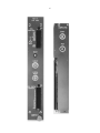
Model AD114
CAMAC 16K ADC
Operating and Service Manual
Printed in U.S.A.
ORTEC® Part No. 762740
Manual Revision E
0305
$GYDQFHG0HDVXUHPHQW7HFKQRORJ\,QF
a/k/a/ ORTEC®, a subsidiary of AMETEK®, Inc.
WARRANTY
ORTEC* warrants that the items will be delivered free from defects in material or workmanship. ORTEC makes
no other warranties, express or implied, and specifically NO WARRANTY OF MERCHANTABILITY OR
FITNESS FOR A PARTICULAR PURPOSE.
ORTEC’s exclusive liability is limited to repairing or replacing at ORTEC’s option, items found by ORTEC to be
defective in workmanship or materials within one year from the date of delivery. ORTEC’s liability on any claim
of any kind, including negligence, loss, or damages arising out of, connected with, or from the performance or
breach thereof, or from the manufacture, sale, delivery, resale, repair, or use of any item or services covered
by this agreement or purchase order, shall in no case exceed the price allocable to the item or service furnished
or any part thereof that gives rise to the claim. In the event ORTEC fails to manufacture or deliver items called
for in this agreement or purchase order, ORTEC’s exclusive liability and buyer’s exclusive remedy shall be
release of the buyer from the obligation to pay the purchase price. In no event shall ORTEC be liable for special
or consequential damages.
Quality Control
Before being approved for shipment, each ORTEC instrument must pass a stringent set of quality control tests
designed to expose any flaws in materials or workmanship. Permanent records of these tests are maintained
for use in warranty repair and as a source of statistical information for design improvements.
Repair Service
If it becomes necessary to return this instrument for repair, it is essential that Customer Services be contacted
in advance of its return so that a Return Authorization Number can be assigned to the unit. Also, ORTEC must
be informed, either in writing, by telephone [(865) 482-4411] or by facsimile transmission [(865) 483-2133], of
the nature of the fault of the instrument being returned and of the model, serial, and revision ("Rev" on rear
panel) numbers. Failure to do so may cause unnecessary delays in getting the unit repaired. The ORTEC
standard procedure requires that instruments returned for repair pass the same quality control tests that are
used for new-production instruments. Instruments that are returned should be packed so that they will withstand
normal transit handling and must be shipped PREPAID via Air Parcel Post or United Parcel Service to the
designated ORTEC repair center. The address label and the package should include the Return Authorization
Number assigned. Instruments being returned that are damaged in transit due to inadequate packing will be
repaired at the sender's expense, and it will be the sender's responsibility to make claim with the shipper.
Instruments not in warranty should follow the same procedure and ORTEC will provide a quotation.
Damage in Transit
Shipments should be examined immediately upon receipt for evidence of external or concealed damage. The
carrier making delivery should be notified immediately of any such damage, since the carrier is normally liable
for damage in shipment. Packing materials, waybills, and other such documentation should be preserved in
order to establish claims. After such notification to the carrier, please notify ORTEC of the circumstances so
that assistance can be provided in making damage claims and in providing replacement equipment, if
necessary.
Copyright © 2005, Advanced Measurement Technology, Inc. All rights reserved.
*ORTEC® is a registered trademark of Advanced Measurement Technology, Inc. All other trademarks used
herein are the property of their respective owners.
iii
CONTENTS
WARRANTY . . . . . . . . . . . . . . . . . . . . . . . . . . . . . . . . . . . . . . . . . . . . . . . . . . . . . . . . . . . . . . . . . . . . . . . . . . ii
SAFETY INSTRUCTIONS AND SYMBOLS . . . . . . . . . . . . . . . . . . . . . . . . . . . . . . . . . . . . . . . . . . . . . . . . . . iv
SAFETY WARNINGS AND CLEANING INSTRUCTIONS . . . . . . . . . . . . . . . . . . . . . . . . . . . . . . . . . . . . . . . v
1. DESCRIPTION . . . . . . . . . . . . . . . . . . . . . . . . . . . . . . . . . . . . . . . . . . . . . . . . . . . . . . . . . . . . . . . . . . . . . . 1
2. SPECIFICATIONS . . . . . . . . . . . . . . . . . . . . . . . . . . . . . . . . . . . . . . . . . . . . . . . . . . . . . . . . . . . . . . . . . . .
2.1. PERFORMANCE . . . . . . . . . . . . . . . . . . . . . . . . . . . . . . . . . . . . . . . . . . . . . . . . . . . . . . . . . . . . . . . .
2.2. CONTROLS AND INDICATORS . . . . . . . . . . . . . . . . . . . . . . . . . . . . . . . . . . . . . . . . . . . . . . . . . . . .
2.3. INPUTS . . . . . . . . . . . . . . . . . . . . . . . . . . . . . . . . . . . . . . . . . . . . . . . . . . . . . . . . . . . . . . . . . . . . . . .
2.4. ECL INPUTS/OUTPUTS . . . . . . . . . . . . . . . . . . . . . . . . . . . . . . . . . . . . . . . . . . . . . . . . . . . . . . . . . .
2.5. CAMAC COMMANDS . . . . . . . . . . . . . . . . . . . . . . . . . . . . . . . . . . . . . . . . . . . . . . . . . . . . . . . . . . . .
2.6. READOUT FORMAT . . . . . . . . . . . . . . . . . . . . . . . . . . . . . . . . . . . . . . . . . . . . . . . . . . . . . . . . . . . . .
2.7. ELECTRICAL AND MECHANICAL . . . . . . . . . . . . . . . . . . . . . . . . . . . . . . . . . . . . . . . . . . . . . . . . . .
2
2
2
2
3
4
6
6
3. INSTALLATION . . . . . . . . . . . . . . . . . . . . . . . . . . . . . . . . . . . . . . . . . . . . . . . . . . . . . . . . . . . . . . . . . . . . .
3.1. INSTALLATION IN CAMAC CRATE . . . . . . . . . . . . . . . . . . . . . . . . . . . . . . . . . . . . . . . . . . . . . . . . .
3.2. AMPLIFIER CONNECTIONS . . . . . . . . . . . . . . . . . . . . . . . . . . . . . . . . . . . . . . . . . . . . . . . . . . . . . . .
3.3. ECL BUS (FERAbus) INSTALLATION . . . . . . . . . . . . . . . . . . . . . . . . . . . . . . . . . . . . . . . . . . . . . . .
3.3.1. ECL BUS RESISTOR PACKS . . . . . . . . . . . . . . . . . . . . . . . . . . . . . . . . . . . . . . . . . . . . . . . .
6
6
6
7
8
4. OPERATION . . . . . . . . . . . . . . . . . . . . . . . . . . . . . . . . . . . . . . . . . . . . . . . . . . . . . . . . . . . . . . . . . . . . . . . . 8
4.1. LOWER-LEVEL DISCRIMINATOR . . . . . . . . . . . . . . . . . . . . . . . . . . . . . . . . . . . . . . . . . . . . . . . . . . 8
4.2. UPPER-LEVEL DISCRIMINATOR . . . . . . . . . . . . . . . . . . . . . . . . . . . . . . . . . . . . . . . . . . . . . . . . . . 8
4.3. PROGRAMMABLE DC-OFFSET . . . . . . . . . . . . . . . . . . . . . . . . . . . . . . . . . . . . . . . . . . . . . . . . . . . . 9
4.4. LIVE-TIME CLOCK . . . . . . . . . . . . . . . . . . . . . . . . . . . . . . . . . . . . . . . . . . . . . . . . . . . . . . . . . . . . . . 9
4.5. ENABLE/DISABLE COMMANDS . . . . . . . . . . . . . . . . . . . . . . . . . . . . . . . . . . . . . . . . . . . . . . . . . . 10
4.6. GATING SIGNALS . . . . . . . . . . . . . . . . . . . . . . . . . . . . . . . . . . . . . . . . . . . . . . . . . . . . . . . . . . . . . . 10
4.7. CONTROL REGISTER . . . . . . . . . . . . . . . . . . . . . . . . . . . . . . . . . . . . . . . . . . . . . . . . . . . . . . . . . . 11
4.8. CONVERTER OPERATION TIMING . . . . . . . . . . . . . . . . . . . . . . . . . . . . . . . . . . . . . . . . . . . . . . . . 11
4.9. READOUT PORT . . . . . . . . . . . . . . . . . . . . . . . . . . . . . . . . . . . . . . . . . . . . . . . . . . . . . . . . . . . . . . . 12
4.9.1. CAMAC READOUT . . . . . . . . . . . . . . . . . . . . . . . . . . . . . . . . . . . . . . . . . . . . . . . . . . . . . . . . 12
4.9.2. ECL PORT (FERAbus) READOUT . . . . . . . . . . . . . . . . . . . . . . . . . . . . . . . . . . . . . . . . . . . 13
4.10. SINGLES MODE . . . . . . . . . . . . . . . . . . . . . . . . . . . . . . . . . . . . . . . . . . . . . . . . . . . . . . . . . . . . . . . 14
5. TROUBLESHOOTING GUIDE . . . . . . . . . . . . . . . . . . . . . . . . . . . . . . . . . . . . . . . . . . . . . . . . . . . . . . . . . 14
APPENDIX A: RECOMMENDED CABLE COMPONENTS . . . . . . . . . . . . . . . . . . . . . . . . . . . . . . . . . . . . . 16
iv
SAFETY INSTRUCTIONS AND SYMBOLS
This manual contains up to three levels of safety instructions that must be observed in order to avoid
personal injury and/or damage to equipment or other property. These are:
DANGER
Indicates a hazard that could result in death or serious bodily harm if the safety instruction
is not observed.
WARNING
Indicates a hazard that could result in bodily harm if the safety instruction is not observed.
CAUTION
Indicates a hazard that could result in property damage if the safety instruction is not
observed.
Please read all safety instructions carefully and make sure you understand them fully before attempting to
use this product.
In addition, the following symbol may appear on the product:
ATTENTION–Refer to Manual
DANGER–High Voltage
Please read all safety instructions carefully and make sure you understand them fully before attempting to
use this product.
v
SAFETY WARNINGS AND CLEANING INSTRUCTIONS
DANGER
Opening the cover of this instrument is likely to expose dangerous voltages. Disconnect the
instrument from all voltage sources while it is being opened.
WARNING Using this instrument in a manner not specified by the manufacturer may impair the
protection provided by the instrument.
Cleaning Instructions
To clean the instrument exterior:
Unplug the instrument from the ac power supply.
Remove loose dust on the outside of the instrument with a lint-free cloth.
Remove remaining dirt with a lint-free cloth dampened in a general-purpose detergent and water
solution. Do not use abrasive cleaners.
CAUTION To prevent moisture inside of the instrument during external cleaning, use only enough liquid
to dampen the cloth or applicator.
Allow the instrument to dry completely before reconnecting it to the power source.
vi
1
ORTEC MODEL AD114
CAMAC 16K ADC
1. DESCRIPTION
The ORTEC Model AD114 CAMAC 16K ADC is a
14-bit ADC with CAMAC and fast FERAbus
readout. It is a very productive solution for
high-multiplicity experiments with germanium
detectors because it has a conversion time of 5 µs
and a 100-ns-per-word FERAbus readout with the
ability to skip ADCs with zero information in 3 ns.
This 16128-channel provides excellent peak
definition when analyzing wide energy ranges with
high-resolution germanium detectors. In fourfold
coincidence experiments, a dead time as low as
15% for each detector channel results in a
coincidence dead-time loss of 48%. Consequently,
the live-time clock included in each Model AD114
is vital for calculating the true coincidence rate. The
flexibility of the computer-controlled functions also
makes the Model AD114 useful for surface barrier
detectors, scintillation detectors, proportional
counters, and ionization chambers.
The dc-coupled analog input employs a peak
amplitude stretcher, and accepts pulses in the
linear range from 0 to +10 V. A 14-bit, successiveapproximation ADC with sliding scale linearization
provides the conversion to a digital number in 5 µs.
The analog input accepts unipolar and bipolar
pulses from standard spectroscopy amplifiers with
shaping times from 0.25 to 20 µs. A differential
input is incorporated to suppress ground-loop noise
when connected to systems with multiple power
supplies and grounds. CAMAC control of the input
dc-offset, the lower-level discriminator, and the
upper-level discriminator facilitates computer
adjustment of the analog operating parameters.
Several types of gating are provided. For
coincidence experiments employing the FERAbus
readout, the master GATE input is delivered to all
ADCs through the ECL CONTROL bus. This gate
synchronizes the ADCs on coincident events and
forces all ADCs to wait for a common Clear at the
end of event readout. In the CAMAC readout mode,
the master GATE can be delivered to all ADCs as
a TTL input on the front-panel LEMO connector.
Using on the master GATE to define coincident
events can lead to the random analysis of unrelated
events at individual ADC inputs. These unwanted
events can be suppressed by providing a LOCAL
GATE input to each ADC only when there is a valid
coincident event at the ADC INPUT. The rear-panel
PUR input is an anticoincidence gate for use with
the pile-up rejector logic pulse from a spectroscopy
input. CAMAC commands permit enabling and
disabling the module's response to the master
GATE or the LOCAL GATE input. This is useful
when selecting the coincidence mode or the singles
mode for the Model AD114 under CAMAC control.
Additional modes selectable by CAMAC command
are: CAMAC or FERAbus readout, zero-suppression or no zero-suppression during readout,
overflow-suppression, and singles or coincidence
analysis.
Each Model AD114 includes its own live-time clock
for correction of dead-time losses. The GedckeHale live-time clock* corrects for the pile-up losses
occurring in the spectroscopy amplifier, and for the
dead time of the ADC conversion and readout. It
provides complete dead-time correction for
amplifiers directly presenting their unipolar output
pulse, and/or amplifiers providing the appropriate
BUSY and PUR logic signals. Via CAMAC
commands, the live-time clock can be reset,
started, stopped, and read without stopping.
The Model AD114 is compatible with the standard
LeCroy FERA control and data output busses. This
system can provide very fast readout of the ADCs
with non-zero events in a CAMAC crate full of
ADCs. For both data acquisition and readout, the
control bus synchronizes all ADCs with the
experiment's master trigger. This permits
identification of all the ADC outputs from the same
event and their subsequent assimilation into a
common block of data. To the standard FERAbus
features, ORTEC has added the ability to select
the singles or coincidence analysis mode for any
Model AD114. This feature allows checking the
*Ron Jenkins, R.W. Gould, and Dale Gedcke, Quantitative XRay Spectrometry (New York: Marcel Dekker, Inc.), 1981, pp.
266-267.
2
functionality of a detector via the singles spectrum
at any time during an experiment. The Model
AD114 can be mixed with the ORTEC Model
AD413A in the same FERAbus readout loop.
Normally, all the ADCs in the crate are connected
to a LeCroy Model 4301 FERA Driver for control
and readout (Fig. 1 on page 8). The FERA Driver,
in turn, delivers the data to either a LeCroy Model
4302 Dual Port Fast Memory in CAMAC, or a CES
Model HSM8170 High Speed Memory in VMEbus.
Both memories operate in the list mode to
assemble the block of coincident events for further
processing by an event builder.
2. SPECIFICATIONS
2.1. PERFORMANCE
ADC ANALOG INPUT Accepts analog input
pulses in the range from 0 to +10 V. The peak
amplitude of an input pulse is converted to a digital
value by a successive-approximation ADC with
sliding scale linearization.
RESOLUTION 16,128 channels (0.625 mV/
channel).
READOUT TIME
Zero-Suppressed Readout Mode Two words at
100 ns per word for FERAbus readout, or at 1 µs
per word for CAMAC readout.
Sequential Readout Mode One word at 100 ns
per word for FERAbus readout, or at 1 µs per word
for CAMAC readout.
CONVERSION TIME 5 µs.
2.2. CONTROLS AND INDICATORS
INTEGRAL NONLINEARITY <±0.025% over the
top 99% of the dynamic range.
DIFFERENTIAL NONLINEARITY <±1% over the
top 99% of the dynamic range.
TEMPERATURE SENSITIVITY 0 TO 50C.
Gain <50 ppm/C.
Zero Offset <50 ppm of full scale per C.
LOWER-LEVEL DISCRIMINATOR RANGE
CAMAC controlled from 0 to 512 mV (2 mV/bit).
CAMAC
UPPER-LEVEL DISCRIMINATOR
controlled from 8.5 V to 10.5 V (8 mV/bit).
CAMAC controlled
DC-OFFSET RANGE
adjustment of input dc-offset from -40 mV to +40
mV (0.312 mV/bit).
LIVE-TIME CLOCK CAMAC controlled GedckeHale Live-Time Clock* with a maximum count of
167772.16 seconds (1.94 days) and a resolution of
10 ms. Readable without interruption.
CAMAC CONTROL OF READOUT MODES
Selection of: CAMAC or FERAbus (ECL bus)
readout, sequential readout of all ADCs or
suppression of ADCs with zeros (zero-suppression
mode), overflow-suppression option, and singles or
coincidence modes.
BUSY Front-panel, multi-color LED, indicates the
percent of the time the ADC is busy. LED appears
green for 0-40%, yellow for 40-70%, and red for
>70% busy.
PD Two front-panel red LEDs, one for the ECL
CONTROL connector, and one for the ECL DATA
OUTPUT connector. Turned on when the ECL
pull-down resistors or termination resistors are
installed for the respective connector.
2.3. INPUTS
INPUT Front-panel BNC connector accepts analog
pulses for pulse amplitude digitization in the linear
range from 0 to +10 V. Input signals can be
positive unipolar pulses, positive gated integrator
pulses, or bipolar pulses (with the positive lobe
leading). Pulse shapes can be semi-Gaussian or
triangular, with shaping time constants from 0.25 to
20 µs, or delay-line-shaped with widths >0.25 µs.
Maximum input is ±12 V. No internal delay. Center
conductor input impedance is 2000 to ground,
dc-coupled. The floating BNC connector shield is
used with a differential input amplifier to suppress
common-mode input noise caused by ground
loops. The common-mode rejection ratio is
nominally 99:1 with a zero-impedance source, and
nominally 22:1 with a 93- signal source.
3
Front-panel BNC connector
LOCAL GATE
provides separate gating for the analog input. A low
TTL logic level (0 to +0.8 V) prevents analysis of
the analog signal at the INPUT connector; a high
TTL logic level (+2 to +5 V) permits analysis of the
analog signal. Resides in the high state with no
input connected. The LOCAL GATE signal must be
at the desired logic level prior to the peak amplitude
of the analog pulse, and must extend 0.5 µ s
beyond peak detection. Input impedance is 1000
. Response to the LOCAL GATE connector can
be enabled/disabled by CAMAC commands.
GATE Front-panel LEMO connector accepts the
master gate signal for coincidence mode operation
with CAMAC readout. See ECL GATE for function.
A low TTL logic level (0 to +0.8 V) prevents
analysis, a high TTL logic level (+2 to +5 V) permits
analysis. Resides in the low state with no input
connected. Input impedance is 1000 .
PUR Rear-panel BNC connector accepts the
pile-up rejector logic signal from the spectroscopy
amplifier supplying the analog input pulses. A high
TTL logic level (+2 to +5 V) causes rejection of the
analog signal; a low TTL logic level (0 to + 0.8 V)
permits analysis of the analog signal. Defaults to a
low state with no input connected. For required
timing, see LOCAL GATE. Input impedance is
1000 .
BUSY Rear-panel BNC connector accepts the
Busy output logic signal from the spectroscopy
amplifier supplying the analog input pulses. Either
a high TTL logic level (+2 to +5 V) at the BUSY
input, or the analog input pulse exceeding the ADC
lower-level discriminator will cause the live-time
clock to start counting backwards. The live-time
clock turns off when the stretcher detects peak
amplitude on the analog impulse, or when a PUR
input occurs. The live-time clock resumes counting
forward after BUSY, PUR, and the lower-level
discriminator all become inactive, and readout of
the conversion has been completed. The BUSY
input is inactive at a low TTL logic level (0 to + 0.8
V) when no input is connected. Input impedance is
1000 .
2.4. ECL INPUTS/OUTPUTS
The fast FERAbus readout utilizes the front-panel
ECL CONTROL bus and the ECL DATA OUTPUT
bus. Differential input impedances are 100 with
termination resistors installed. Only one module
should have the termination and pull-down resistors
installed (See PD LED and Fig. 1).
ECL LOGIC LEVELS Nominal differential ECL
logic levels (into 100- differential load) are:
Left (+) Pin
Logic 0
Logic 1
-1.8 V
-0.9 V
Right (-) Pin
-0.9 V
-1.8 V
ECL DATA OUTPUT Front-panel 17- by 2-pin
connector (AMP 1-103326-7) provides the digitized
ADC outputs for connection to the FERA data
readout bus. Differential ECL outputs are employed,
with bit 1 assigned to the two pins in row 1, and bit
16 occupying the two pins in row 16. Row 17 is not
connected. S e e R E A D OU T FORMAT.
Interconnection between ADC modules and the
FERA Driver (LeCroy 4301) requires construction of
a 34-conductor ribbon cable (3M part number
3365/34) with 17- by 2-pin headers (3M 3414- 6006
or AMP 499498-9) spaced to match the
configuration of modules (Fig. 1).
ECL CONTROL BUS Front-panel 8- by 2-pin
connector accommodates the control bus for
synchronizing data acquisition among multiple
ADCs, and for ECL readout. Except where noted
otherwise, the inputs to the AD114 are provided
from the LeCroy 4301 FERA Driver connected to
the bus. A row of two pins is assigned to each
differential ECL input or output. Interconnection
between ADC modules and the FERA Driver
(LeCroy 4301) requires construction of a
16-conductor ribbon cable (3M part number
3365/16) with 8- by 2-pin headers (3M 3452-6006
or AMP 499497-3)
spaced
to match the
configuration of modules (Fig. 1). The logic signals
in the ECL CONTROL bus are listed below.
N/C No connection.
WST The Write Strobe output indicates when each
output word is valid on the ECL DATA OUTPUT
connector. WST is released 15 ns after the Write
Acknowledge (WAK) is received.
REQ The Request output indicates that the module
has completed its conversions, and is ready to take
control of the ECL DATA OUTPUT bus for readout.
REQ can be asserted only if FERAbus readout is
enabled.
CLR Clears stored data and conversions in
progress for all ADCs connected to the ECL
CONTROL bus. Required in the coincidence mode
4
at the end of readout to simultaneously release all
ADCs for the next conversion. CLR is not required
in the singles mode. Minimum width, 5 ns. Clear
can also be initiated from the CAMAC interface. If
Clear is asserted during ADC conversion, up to 5
µs are required to clear the module.
GATE The Gate input simultaneously provides the
master gate signal to all ADCs connected to the
ECL CONTROL bus for coincidence mode
operation. The logic 1 state enables acceptance of
the analog input signal for conversion, and forces
all ADCs to wait for a common clear (CLR) after
analyzing coincident events. With no signal
connected, the GATE input remains in the logic 0
state. See LOCAL GATE for required timing. The
ECL GATE input is OR'ed with the TTL GATE input
from the LEMO connector. Response to the GATE
input can be enabled/disabled by CAMAC
commands.
The Write Acknowledge input signal
WAK
indicates through the readout controller (LeCroy
4301) that the associated memory has read the
current word and that the next word may be sent.
WAK minimum width is 30 ns.
2.5. CAMAC COMMANDS
Z
Initializes module. Clears the module,
sets all bits of control register to zero,
sets LLD register to 36 (72 mV), sets
ULD register to 255 (10.5 V), sets
offset to 128 (0 V), enables the ADC
(F(26)·A(0)), and clears the live-time
clock.
C
Performs the same function as the CLR
input.
I
Inhibits subsequent conversions and
stops the live-time clock when
asserted. Conversions and readouts
already in progress are not affected.
Used to start and stop data acquisition
on all ADCs in the CAMAC crate at the
same time.
X
Generated by the module for all valid
functions.
Q
Generated by the module if the function
can be executed.
L
Indicated LAM is set. Occurs after the
end of conversion, if there are data to
be read (provided CAMAC readout is
enabled, and LAM is enabled). See
CONTROL REGISTER FORMAT.
GND Connected to ground.
N/C No connection.
REN The Readout Enable input is a front-panel, 1by 2-pin connector. It accepts the PASS output
from a previous module, or the REO output from
the LeCroy 4301, to enable readout of the Model
AD114. Interconnection requires construction of a
100-, twisted-pair cable with a 2-pin socket and
housing (AMP 1-87756-8 and AMP 5- 87456-3) on
each end.
PASS The PASS output is provided on a
front-panel, 1- by 2-pin connector. It indicates
completion of the module's readout cycle on the
ECL bus. The PASS output is normally connected
to the REN input on the next module to enable
readout of the next module (Fig. 1). In the zerosuppression mode, the Model AD114 generates
the PASS signal typically within 3 ns of receiving
the REN signal if the Model AD114 has no data to
read out. The PASS signal from the last Model
AD114 in the readout loop is used to generate the
CLR signal via the external master trigger logic for
the experiment and/or the LeCroy 4301.
F(0)·A(0)
Read Control Register.
F(1)·A(0)
Read lower-level discriminator (LLD)
setting. The value returned is in units of
2 mV. Only the low 8-bits are valid.
F(1)·A(1)
Read upper-level discriminator (ULD)
setting. Multiply the low 8-bits of the
value read by 8 mV and add 8.5 V to
calculate the voltage setting.
F(1)·A(2)
Read the input dc-offset setting.
Subtract 128 from the lower 8 bits and
multiply the resulting 8-bit number by
0.312 mV to calculate the voltage
setting.
F(2)·A(0)
Read ADC converted digital output. If
the zero-suppression mode is disabled
(Control Register B9 = 1) and CAMAC
readout mode is selected (B10 = 1), the
command is issued once to read the
ADC data. If zero-suppression is
enabled with CAMAC readout mode
5
(B10 = 1), the command is issued
twice, or until Q = 0. Q = 1 for a valid
readout.
F(3)·A(0)
Read low 16-bits of the live-time clock.
The value is returned in units of 10 ms.
When this command is issued, the
highest 8 bits of the live-time clock are
simultaneously captured and stored for
a subsequent F(3)·A(1) command.
CONTROL REGISTER FORMAT
Bit
Function
B1 to B8
Virtual Station Number. Index Source
for readout with zero-suppression.
(Lower eight bits of header word.)
B9
Read the higher 8 bits of the live-time
clock. This command reports the value
of the higher 8 bits captured by the last
F(3)·A(0) command.
Zero-suppression enable. When B9 =
0, ADCs with zeros for data are
skipped during readout.
B10
ECL port enable. When B10 = 0, ECL
port readout is enabled. When B10 = 1,
CAMAC readout is enabled.
F(8)·A(0)
Test LAM. Q = 1 if LAM is present.
B11
F(9)·A(0)
Clear Module. Performs the same
function as the C command, except
only for the single module being
addressed through CAMAC.
Enable LOCAL GATE (B11 = 0). When
B11 = 1, the LOCAL GATE input is
ignored and all analog pulses are
converted, unless gated by the master
GATE or by PUR.
B12
Enable master GATE (B12 = 0) for the
coincidence mode. When B12 = 1, the
master GATE signal is ignored, and all
analog pulses are converted, unless
gated by LOCAL GATE or by PUR. B12
= 1 is used only in conjunction with the
singles mode (B13 = 1).
B13
Selects the Coincidence mode or the
Singles mode. When B13 = 0, the
coincidence mode is selected. When
B1 =1, the singles mode is selected.
When in the singles mode, the zerosuppression mode must be selected for
all ADCs, if the FERAbus readout loop
includes more than one ADC.
B14
Not used.
B15
CAMAC LAM enable. When B15 = 1,
LAM is enabled.
B16
Overflow-suppression enable. When
B16 = 0, overflows are converted to
zeros in the ADC output data. Readout
will be suppressed only if the zerosuppression mode (B9 = 0) is selected.
F(3)·A(1)
F(10)·A(0) Test and clear LAM. Q = 1 if LAM is
active.
F(12)·A(0) Reset the live-time clock to zero.
F(16)·A(0) Write into the Control Register.
F(17)·A(0) Write LLD value. See F(1)·A(0) for
format.
F(17)·A(1) Write ULD value. See F(1)·A(1) for
format.
F(17)·A(2) Write input dc-offset value. See
F(1)·A(2) for format.
F(24)·A(0) Disable ADC. Performs the same
function as the Inhibit (I) command, but
only for the addressed ADC. Stops the
live-time clock and prevents
conversions from occurring until
F(26)·A(0) is issued.
F(26)·A(0) Enable the ADC. Enables conversions
and starts the live-time clock when the
Inhibit (I) command is not active.
current
status
of
F(27)·A(0) T e s t
ENABLE/DISABLE flag as set by the
F(26)·A(0) and F(24)·A(0) commands.
Q = 1 if the ADC enabled.
6
2.6. READOUT FORMAT
DEFINITIONS
The readout format of the AD114 is identical in both
the CAMAC and the FERAbus ECL readout modes.
WITHOUT ZERO-SUPPRESSION
B16
B15
B14 . . . . . . . . . . . . . . . . . . . B1
0
0
DATA
WRDCNT The word count defines the number of
data records that follow the header word. The word
count is always 01 for a Model AD114.
VSN The Virtual Station Number (0-255) identifies
the module number during zero-suppressed
readout. VSN is set via CAMAC command in the
lower 8 bits of the Control Register.
DATA Fourteen bits of ADC conversion data.
DATA over 16128 indicates overflow.
WITH ZERO-SUPPRESSION
When zero-suppression is enabled and valid data
are received, two data words are output. The first is
always a Header word:
B16
B15
B14
B13 ... B12
B11
B10
B9
B8 ... B1
1
0
0
WRDCNT
0
0
0
VSN
Followed by one data record, with the following
format:
B16
B15
B14 . . . . . . . . . . . . . . . . . . B1
0
0
DATA
2.7. ELECTRICAL AND MECHANICAL
POWER REQUIRED The Model AD114 derives its
power from a CAMAC crate supplying ±24 V and
±6 V. The power required is +24 V at 160 mA, +6 V
at 1.4 A, -6 V at 0.9 A, and -24 V at 170 mA.
WEIGHT
Net 1.1 kg (2.5 lb).
Shipping 2.0 kg (4.5 lb).
CAMAC-standard double-width
DIMENSIONS
×
module, 3.42
22.15 cm (1.35 × 8.72 in.) front
panel per IEEE/583-1975.
3. INSTALLATION
3.1. INSTALLATION IN CAMAC CRATE
3.2. AMPLIFIER CONNECTIONS
The AD114 may be placed in any available slot in
a CAMAC crate except for the slot which is
reserved for the crate controller (usually slot 25).
The power to the crate should ALWAYS be turned
off when inserting and removing modules to
prevent problems associated with momentary
misalignment of the card edge connections.
In a standard electronics setup, the AD114 has
three connections to an associated amplifier. The
input, on the front panel of the AD114, is normally
connected to the output of the amplifier. The PUR
input on the rear panel of the AD114, which is used
to reject pulses that are too close together to be
properly processed with the selected pulse shaping
time, is normally connected to the amplifier pile-up
reject output, labeled PUR or INHIBIT. The BUSY
input on the rear panel of the AD114, which is used
to provide proper live-time correction, is connected
to the busy output on the amplifier. The following
chart shows the normal connections to various
ORTEC amplifiers.
With the power to the crate turned off, slide the
module into any available slot and tighten the jack
screw on the bottom front of the module to force the
card edge connector into the CAMAC bus. The
AD114 requires two CAMAC slots; however, the
module responds only to CAMAC functions issued
to the higher number slot. For example, if the
AD114 occupies slots 10 and 11, the AD114
responds to commands issued to slot 11, but not
slot 10.
7
AD114 Amplifier Connections
AMPLIFIER
ORTEC MODEL 572
ORTEC MODEL 671
ORTEC MODEL 672
ORTEC MODEL 673
ORTEC MODEL 973
IN
UNI or BI
UNI or BI
UNIPOLAR or BIPOLAR
UNIPOLAR or GI
OUTPUT or GI
PUR
INH
PUR
PUR
INHIBIT
PUR
BUSY
BUSY
BUSY
BUSY
BUSY
BUSY
If a transistor-reset preamplifier (TRP) is connected
to the detector, PUR must be connected differently.
If a Model 572 or 673 amplifier is used, connect
PUR on the AD114 to the INHIBIT OUTPUT on the
Model 132 inhibit generator, and connect INHIBIT
on the amplifier to INHIBIT INPUT on the Model
132. If a Model 671, 672, or 973 amplifier is used,
connect INHIBIT OUTPUT on Model 132 to
INHIBIT INPUT on the amplifier, and connect PUR
on the amplifier to PUR on the AD114.
If a Model FG424 fine-gain and offset controller is
in the system, the amplifier output connects to the
FG424 input and the FG424 output connects to the
AD114 input. The PUR and BUSY connections are
unchanged. Refer to the specifications in Section 2
for further details concerning the INPUT, PUR, and
BUSY inputs.
3.3. ECL BUS (FERAbus) INSTALLATION
If only CAMAC readout will be used, and FERAbus
readout will not be used, then ECL bus installation
is not necessary.
An ECL bus interface is provided on the AD114 for
high-speed readout of ADC data. The ECL bus is
designed to permit multiple ADCs to be connected
to the bus in parallel for readout of a large number
of channels. A wiring diagram for a multiple ADC
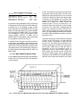
system is shown in Figure 1. Across the top of all
modules is a control bus, which controls the
readout process. The bus is formed from a 16conductor ribbon cable with an 8- by 2-pin header
mounted on it for each ADC. Located across the
bottom of the modules is the ECL OUTPUT bus.
This bus is formed with a 34-conductor ribbon cable
with 17- by 2-pin headers mounted on the cable for
each ADC. REN and PASS are normally connected
as shown in Fig. 1.
In the first module in the chain, REN is connected
to REO on the FERA driver. On the remaining
modules, REN is connected to PASS from the
previous unit. The PASS output on the final unit is
normally connected to the Clear (CLI) input on the
LeCroy 4301 FERA driver to clear the ADCs in
preparation for the next coincidence event. In
experiments with an event master trigger, the
PASS output from the final AD114 may be sent
through the master trigger logic to generate the
Clear input for the FERA driver. The ORTEC Model
AD413A can be mixed with the AD114 in the same
Fig. 1. Interconnection of Multiple Model AD114s and the LeCroy 4301 FERA Driver for FERAbus Readout.
8
FERAbus readout loop. The connections are the
same. See Appendix A for information on cables.
3.3.1. ECL BUS RESISTOR PACKS
If an acquisition system makes use of multiple
AD114 modules connected together with an ECL
bus, the resistor packs must be removed from all
except the last module in the chain of modules. The
PD LEDs on the front panel of the AD114 are lit
when the resistor packs are installed. Figure 1
indicates which module in a chain of modules
should have the packs installed.
To remove the resistor packs from a module do the
following:
1. Turn off power to CAMAC crate and
remove AD114 module after disconnecting
all cables.
2. Slide the left side plate back approximately
4 inches to reveal the components near the
front panel of the module.
3. Locate resistor packs labeled RA3, RA4,
RA5, RA6, RA7, RA8 and RA9 by referring
to the Main Component Assembly Drawing
at end of this manual. Remove the resistor
packs from their sockets.
4. Store the resistor packs in a safe location,
so they can be found and replaced, if
necessary.
5. Close the side panel and return the module
to the CAMAC crate.
Should it become necessary to replace the resistor
packs once they have been removed, refer to
Table 3.1 to determine which types belong in each
location. Make sure to orient the resistor packs
correctly before insertion into the socket. In the
Main Component Assembly Drawing, pin 1 is
indicated with a bar across the pack and a small
"1". On most resistor packs, pin 1 is indicated with
a dot.
Table 3.1. Resistor Pack Values.
Resistor Pack
Value ( )
RA3, RA4, RA5, RA6
RA7
RA8
RA9
470
470
56
2200
No. of Pins
10
6
8
6
NOTE: When reading values on resistor packs,
470 is often designated 471, 56 is often designated
560, and 2200 is usually designated 222.
4. OPERATION
4.1. LOWER-LEVEL DISCRIMINATOR
The Model AD114 has a programmable lower-level
discriminator (LLD) setting. This voltage level
determines the minimum amplitude pulse that will
be accepted by the ADC. Normally the lower-level
is set just above the level of the noise in the
system, so time is not wasted converting noise
pulses.
The lower level in the AD114 is set with the
CAMAC command F(17)·A(0). An 8-bit value is
written to the module during this CAMAC command
specifying the voltage in units of 2 mV. A value of
50 in the lower-level register sets the voltage to 100
mV. The lower-level setting may be read with the
F(1)·A(0) CAMAC command. The returned 8-bit
value is also in units of 2 mV. When reading the
lower-level setting, only the low 8 bits are valid. Any
higher bits should be ignored. The high bits may be
cleared by performing an AND function between
the returned value and 255 decimal. (e.g., in
BASIC, INFO = INFO AND 255)
The CAMAC commands that change and report the
lower level are active only when the ADC is not
busy. The ADC is not busy after a clear command
and before the peak of the next acceptable pulse
after the clear. No Q response is given if the ADC
is busy when the commands are issued. To
guarantee that the ADC is not busy, set the CAMAC
inhibit line (I) and clear the module (C command).
The initial setting of the lower-level voltage on
initialization (Z command) is 36, which corresponds
to 72 mV.
4.2. UPPER-LEVEL DISCRIMINATOR
The Model AD114 has a programmable upper-level
discriminator (ULD) setting. This voltage level
determines the maximum amplitude pulse that will
be accepted by the ADC. Normally the upper-level
is set just above the 10 V level, so time is not
wasted converting over-range pulses.
9
The upper-level in the AD114 is set with the
CAMAC command F(17)·A(1). An 8-bit value is
written to the module during this CAMAC command
specifying the voltage in units of 8 mV with an
offset of 8.5 V. A value of 200 in the lower-level
register sets the voltage to 8.5 + 0.008 × 200 =
10.1 V. The upper-level setting may be read with
the F(1)·A(1) CAMAC command. The returned 8-bit
value is also in units of 8 mV with an 8.5 V offset.
When reading the upper-level setting, only the
low 8 bits are valid. Any higher bits should be
ignored. The high bits may be cleared by
performing an AND function between the returned
value and 255 decimal. (e.g., in BASIC, INFO =
INFO AND 255).
The CAMAC commands that change and report the
upper-level are active only when the ADC is not
busy. The ADC is not busy after a clear command
and before the peak of the next acceptable pulse
after the clear. No Q response is given if the ADC
is busy when the commands are issued. To
guarantee that the ADC is not busy, set the CAMAC
inhibit line (I) and clear the module (C command).
The initial setting of the upper-level voltage on
initialization (Z command) is 255, which
corresponds to 10.54 V.
4.3. PROGRAMMABLE DC-OFFSET
The Model AD114 has a programmable input dcoffset adjustment. This voltage level is summed
with the input signal just before conversion of the
signal. Normally the offset is set to 0 V. Setting the
offset to a value other than 0 will have the effect of
shifting the entire spectrum by the offset value. The
offset voltage is set with the CAMAC command
F(17)·A(2). An 8-bit value is written to the module
during this CAMAC command specifying the
voltage in units of 312 µV with an offset of -40 mV.
A value of 200 in the offset register sets the voltage
to -40 + 0.312 × 200 = 22.4 mV. The offset setting
may be read with the F(1)·A(2) CAMAC command.
The returned 8-bit value may be translated to
voltage by subtracting 128 and then multiplying by
0.312 mV. When reading the offset setting, only the
low 8 bits are valid. Any higher bits should be
ignored. The high bits may be cleared by
performing an AND function between the returned
value and 255 decimal. (e.g., in BASIC, INFO =
INFO AND 255).
The CAMAC commands that change and report the
offset are active only when the ADC is not busy.
The ADC is not busy after a clear command and
before the peak of the next acceptable pulse after
the clear. No Q response is given if the ADC is
busy when the commands are issued. To
guarantee that the ADC is not busy, set the CAMAC
inhibit line (I) and clear the module (C command).
The initial setting of the offset voltage upon
initialization (Z command) is 128, which
corresponds to 0 V.
4.4. LIVE-TIME CLOCK
The Model AD114 is equipped with a Gedcke-Hale
Live-Time Clock which is 24-bits in length with a
resolution of 10 ms. After the live time reaches
167,772.15 seconds (1 day, 22 hours, 36 minutes
and 12.15 seconds), the live time returns to zero
and starts over. The live time may be read by
issuing the F(3)·A(0) and F(3)·A(1) commands.
F(3)·A(0) returns the low 16-bits of the live time and
also latches the high byte of the live time. F(3)·A(1)
returns the high byte of the live time which was
latched by the F(3)·A(0) command. If F(3)·A(1)
commands are repetitively issued, they will always
return the same value because no new data is
being latched by the F(3)·A(0) command. When
reading the high byte of the live time, only the low
8 bits of the returned word are valid. Any higher bits
should be ignored. The high bits may be cleared by
performing an AND function between the returned
value and 255 decimal. (e.g., in BASIC, INFO =
INFO AND 255).
The live-time clock may be set to zero with the
F(12)·A(0) command or by initializing (Z) the
CAMAC crate. The live-time clock may be paused
by setting the inhibit line (I) in the CAMAC crate or
by disabling the ADC (see Section 4.5.).
The CAMAC commands that report the live time
are active only when the ADC is not busy. The ADC
is not busy after a clear command and before the
peak of the next acceptable pulse after the clear. A
No-Q response is returned if the ADC is busy when
the commands are issued. A No-Q response is also
returned if the live-time clock was incremented 1 µs
or less before the F(12)·A(0) command is given.
This prevents unstable data from being read. To
guarantee a valid read, set the CAMAC inhibit line
(I) and clear the module (C command) before
reading the live time.
The Gedcke-Hale Live-Time Clock is intended for
use with the unmodified, unipolar, analog output
pulses from a spectroscopy amplifier. It uses the
amplifier pulse shape information, along with the
amplifier BUSY and PUR (pile-up reject) signals to
10
compensate for the dead-time losses caused by
pile-up in the spectroscopy amplifier. In order to
calculate the effective live time, the dead-time
correction for pile-up losses in the amplifier is
added to the correction for the AD114 conversion
and readout dead time. When the counts in a fullenergy peak in the energy spectrum are divided by
the live time, the resulting counting rate is an
accurate estimate of the true counting rate for that
gamma-ray energy at the input to the preamplifier.
The live-time clock works with unipolar pulse
shapes from gated integrators, Gaussian shaping
amplifiers, triangular pulse shaping amplifiers, and
single-delay-line shaping amplifiers. Best results
are obtained when the BUSY and PUR signals from
the amplifier are connected to their respective
inputs on the Model AD114.
The Gedcke-Hale Live-Time Clock works as
follows. Either the leading edge of the BUSY signal
from the amplifier, or the amplifier analog pulse
exceeding the Model AD114 lower-level
discriminator will cause the live-time clock to start
counting backwards. The live-time clock turns off
when the stretcher in the Model AD114 detects
peak amplitude on the analog input pulse, or when
a PUR input occurs. The live-time clock resumes
counting forward after BUSY, PUR, and the lowerlevel discriminator all become inactive, and readout
of the conversion has been completed. Turning off
the live-time clock compensates for the probability
of losing a second pulse after responding to the first
pulse. Subtracting live time compensates for the
probability of losing both the first and the second
pulses from the full- energy peak in the spectrum,
as a result of the second pulse piling up and
distorting the peak amplitude of the first pulse.
Turning off the clock compensates for losing one
pulse, while counting backwards provides double
weighting and compensates for the loss of two
pulses.
The Gedcke-Hale Live-Time Clock will work with
bipolar pulses, or with amplifiers that pass only a
portion of their signal through a linear gate, if the
appropriate signals are supplied to the AD114
BUSY and PUR inputs. The BUSY and PUR
signals must accomplish the functions described in
the paragraph above. See the ORTEC Model 675
Operating and Service Manual, for example.
4.5. ENABLE/DISABLE COMMANDS
The CAMAC commands F(24)·A(0), F(26)·A(0), and
F(27)·A(0) control the DISABLE ADC signal in the
AD114. The DISABLE ADC signal performs the
same function as the inhibit (I) signal in the CAMAC
crate, but it only affects the addressed AD114. If
the inhibit signal is set, all modules in the crate are
inhibited. If the DISABLE ADC signal is set, only the
AD114 which received the command is inhibited.
To disable the AD114, issue the F(24)·A(0)
command. To enable the AD114, issue the
F(26)·A(0) command. To determine the current
state of the DISABLE ADC signal, issue the
F(27)·A(0) command, if the AD114 is enabled, a Q
= 1 response is generated; otherwise, no Q is
generated.
When the AD114 is disabled, the live-time clock is
paused and no pulses are accepted for conversion.
4.6. GATING SIGNALS
Three input signals are available to select which
pulses are to be converted by the ADC: PUR,
LOCAL GATE, and the master GATE. If any one of
the signals indicates that the pulse is to be rejected,
the pulse will be rejected. All three inputs are
sampled approximately 100 ns after the peak of an
input pulse; therefore, the gating signals should
arrive before the peak of the pulse and extend at
least 500 ns beyond the peak to ensure proper
sampling.
PUR or pile-up reject is always active and is
normally connected to the pile-up reject output on
an amplifier associated with the channel. When the
PUR input is high, pulses are not converted. The
PUR input assumes a low state when no
connection is made to the PUR input. The PUR
input can also be used as a general-purpose veto
or anticoincidence input.
LOCAL GATE is an individual gate input. The
LOCAL GATE can be used in addition to the master
GATE to ensure that each ADC accepts only pulses
that are judged to be valid for that ADC input.
LOCAL GATE may be disabled by setting the
appropriate bit in the control word (see Section
4.7). If the LOCAL GATE is enabled, pulses are
converted only if the gate signal is high. The GATE
input assumes a high state when no connection is
made to the GATE input.
The master GATE signal may be supplied via the
ECL control bus or the LEMO connector on the
front panel. Normally the master GATE is
distributed to all ADC modules in a system. The
master GATE signal not only provides a gating
function, it also determines which pulses are to be
grouped together as a coincident event. When the
11
master GATE is high, pulses are accepted into the
AD114. When the master GATE returns low, no
pulses are accepted into the ADC until a Clear
command is given, even if the master GATE
returns high. The master GATE may be disabled in
the AD114 by setting bit 12 in the control word (see
Section 4.7). Disabling the master GATE is invalid
for coincidence experiments, because there is no
signal to indicate which pulses belong in the
coincident event. Disabling the master GATE is
useful only when collecting singles spectra.
4.7. CONTROL REGISTER
The control register in the AD114 determines the
various modes of operation. The control register
specifies the virtual station number of the module
as well as the readout modes, operation modes
and which gating signals are to be enabled.
The Control register is loaded with the CAMAC
function F(16)·A(0), and is queried with the CAMAC
function F(0)·A(0). These CAMAC commands are
active only when the ADC is not busy. The ADC is
not busy after a clear command and before the
peak of the next acceptable pulse after the clear.
No Q response is given if the ADC is busy when the
commands are issued. To guarantee that the ADC
is not busy, set the CAMAC inhibit line (I) and
clear the module (C command).
The lower 8 bits of the control register form the
virtual station number for the module. The
remaining bits in the control register have the
following function:
Zero-Suppression Enable (Bit 9) Specifies zerosuppression readout mode as opposed to
sequential mode (ECL PORT or CAMAC).
= 0;
Zero-suppression selected.
= 1;
Sequential selected.
ECL Port Enable (Bit 10) Specifies which readout
port is to be used; CAMAC or ECL.
= 0;
ECL readout enabled.
= 1;
CAMAC readout enabled.
Enable LOCAL GATE (Bit 11)
= 0;
Front-panel LOCAL GATE enabled.
= 1;
LOCAL GATE disabled.
Enable MASTER GATE (Bit 12)
= 0;
Master GATE is enabled.
= 1;
Master GATE is disabled. This mode
should not be selected while in the
coincidence mode of operation
because the master GATE determines
which pulses belong in an event. This
mode should be used only in the
singles mode.
Coincidence/Singles Mode Select (Bit 13)
Specifies coincidence mode or singles mode.
= 0;
Coincidence mode selected.
= 1;
Singles mode selected. See
Section 4.10.
CAMAC LAM Enable (Bit 15) Specifies if LAM is
to be asserted when data is ready to be readout on
the CAMAC port.
= 0;
LAM is not asserted.
= 1;
LAM is asserted if CAMAC readout is
selected.
Overflow-Suppression Enable (Bit 16) Specifies
overflow-suppression mode.
= 0;
Overflow-suppression enabled. When
used in conjunction with zerosuppression mode, pulses above the
upper-level discriminator are not
reported. When not in zerosuppression mode, pulses above the
upper-level discriminator are reported
as zero.
= 1;
Overflow-suppression disabled. All
pulses above the upper-level
discriminator are reported with a value
between 16128 and 16383.
On power-up, the control registers have an
undetermined value. If an initialize (Z) command is
issued to the CAMAC crate, all bits of the control
registers are set to zero.
4.8. CONVERTER OPERATION TIMING
Figure 2 illustrates the conversion and readout
timing when a pulse is accepted into the module.
The conversion process begins as soon as a peak
detect occurs. The conversion phase then takes 5
µs for a valid input. If an input is rejected by the
upper-level discriminator, Pile-Up Rejector, the
LOCAL GATE, or the lower-level discriminator, no
time is required during T1 for that channel.
When the conversion phase completes AND the
master GATE has returned low, the readout phase
begins. The time required to read out depends on
the readout method and the mode selected. See
Fig. 2 for details.
12
Fig. 2. Conversion Timing Diagram.
Once readout completes, a clear command must
be issued by the readout electronics. Once the
clear command is given, the ADC is ready for the
next pulse.
If the Clear command is issued during a
conversion, the conversion process must finish (T1)
before the module can accept another input pulse.
4.9. READOUT PORT
Data from the AD114 can be read from either the
CAMAC interface or the ECL BUS interface. The
ECL BUS interface (FERAbus) is designed for highspeed readout, up to 10 MHZ, and is suited for
bussing many ADC modules together into a large
system. However, additional external hardware
(FERA drivers, FIFO memories, cables, etc.) is
required to buffer the data and transfer it to
permanent storage. When CAMAC readout is
utilized, readout occurs at speeds a factor of 10 or
more slower; however, performing the readout via
CAMAC does not require any extra hardware to get
data out of the ADC and into a host computer.
When the AD114 is initialized, the default readout
method is the ECL BUS. To select the CAMAC
option, bit 10 of the control register should be set
high.
4.9.1. CAMAC READOUT
When CAMAC readout is selected, data is read
from the ADC via CAMAC operations. Two modes
exist for reading data from the module via the
CAMAC interface: "zero suppression," and
"sequential."
In zero-suppression mode, two data words are
available to be read out when a valid pulse is
received. The two words are read by issuing the
F(2)·A(0) CAMAC command twice. The first output
word is the header word that identifies the AD114,
which is reporting data. The format of the header
word is shown in Section 2.6. The data word
follows the header. Issuing the F(2)·A(0) command
a third time will result in a NO-Q response. If
overflow suppression is enabled, no data is
reported for an overflow. If overflow suppression is
disabled, a value greater than 16128 is reported.
Zero-suppression mode is enabled by setting bit 9
of control register 1 to 0.
When sequential readout mode is selected, there is
always 1 data word to be read from the ADC after
an event occurs (master GATE goes high, then
low). The word is read by issuing the F(2)·A(0)
CAMAC command. After the word has been read,
Q = 0 occurs if the command is issued again. If no
13
pulse arrives during the gating time a zero will be
reported. If overflow suppression is enabled, zero
will be reported for an overflow. If overflow
suppression is disabled, a value greater than 16128
is reported. Sequential readout is selected by
setting bit 9 of the control register to 1.
Regardless of the readout mode selected, the
module must be cleared after readout is completed
to permit new conversions, unless singles mode is
selected (see Section 4.10). The clear can be
initiated with the global CAMAC clear function, or
an addressed clear to a single module [F(9)].
If bit 15 in control register 1 is set, a Look-At-Me
(LAM) signal is asserted by the module when data
is ready to be read. The LAM will be cleared when
the last data word is read. The LAM may also be
cleared with the F(10)·A(0) command.
4.9.2. ECL PORT (FERAbus) READOUT
When ECL (FERAbus) readout is selected, data is
read from the ADC via the front panel ECL DATA
port. Multiple AD114 modules may be connected in
parallel on the ECL bus for readout of a large
number of channels. When multiple ADCs are
connected to the ECL bus, a FERA driver module
(LeCroy 4301 or CES 1570) is usually required to
control the bus. Two readout modes exist for ECL
readout: "sequential mode" and "zero suppression
mode."
In sequential mode, one data word is available to
readout after every event. When this mode is used,
every AD114 module in the system will always
report one data word when an event occurs (master
GATE is asserted). The format of the data word can
be found in Section 2.6. If overflow suppression is
enabled, a zero is output in place of the overflow. If
overflow-suppression is disabled, a value greater
than 16128 is output in place of the overflow value.
If no pulse occurs during the gating time or the
pulse is rejected with the PUR, LOCAL GATE or
lower-level discriminator, a zero is output during
readout.
In zero-suppression mode, only non-zero data is
output on the ECL port. If no non-zero data is
available, no data is output onto the ECL bus. If
there is data to be read, the module outputs a
header word, which contains the virtual station
number of the ADC, and then the data word.
Therefore, when an ADC module receives non-zero
data, two data words are output on the bus; no data
is placed on the bus if the data is zero. Zero-
suppression mode is the mode of choice in most
experiments, because time is not wasted reading
zeros out of modules that did not convert a pulse
during the event. The ECL readout passes by an
ADC with zeros typically within 3 ns in the zerosuppression mode. If an input pulse is rejected with
the LOCAL GATE, PUR, or lower-level
discriminator, no data is reported.
Regardless of the readout mode selected, the
module must be cleared after readout to permit new
conversions, unless the singles mode is used (see
Section 4.10). The clear can be initiated with the
global CAMAC clear function, an addressed clear
to a single module [F(9)], or a clear from the ECL
control bus on the front panel.
Five different control signals are used to control
ECL PORT readout. A description of each follows,
and their relationship can be observed in Fig. 3.
REQ (Output) The readout request signal is
asserted by the AD114 as soon as data are ready
for readout. REQ is removed when the last datum
has been read or a clear command is given.
REN (Input) The readout enable input causes an
AD114 to begin readout if it has data ready to be
output. Once REN is asserted, it must remain active
throughout the entire readout cycle.
PASS (Output) The pass output is asserted by
the AD114 when REN is asserted, if the module is
not busy converting, and if the module does not
have any data to output. The AD114 will not
generate a PASS signal as long as it is busy
converting new data. This feature allows ADCs with
different conversion times to be placed in the same
FERA readout loop without additional logic
hardware.
WST (Output) The write strobe output is asserted
by the AD114 when a data word is available on the
ECL port output. The data is stable on the output a
minimum of 15 ns before the write strobe occurs,
and the write strobe continues to be asserted a
minimum of 15 ns after the write acknowledge
signal has occurred.
The write acknowledge input is
WAK (Input)
asserted by the readout controller when the data on
the ECL port output has been accepted. WAK
should be removed after WST has been released.
WST is not reasserted after WAK has been
released until 50 ns have elapsed.
14
4.10. SINGLES MODE
Although this module is designed with coincidence
experiments in mind, a mode exists for collection of
singles data. When bit 13 is set in the control
register (see Section 2.6), the module behaves in a
fashion that can be used to collect a singles
spectrum. The major distinction of singles mode is
that no clear is required to reset the module once
readout has completed. The module performs its
own clear. This enables one module to be read out
and cleared without affecting any other modules in
the chain. A second distinction of the singles mode
is that data is read out after each conversion
completes. In coincidence mode, readout will not
occur until the master GATE has returned low;
however, when the singles mode is enabled, the
master GATE has no "grouping effect." Data
readout is immediately initiated by a module when
conversion is complete regardless of the state of
the master GATE.
Normally, the master GATE is disabled on units that
are placed in the singles mode by setting bit 12 of
the control register. Then, if singles data collection
is desired in selected modules in a readout chain,
the unselected modules can be inhibited by
suppressing the gate input to the FERA driver. In a
readout chain, either singles mode or coincidence
mode should be used in all modules, not a
combination of modules in singles mode and
coincidence mode.
Fig. 3. ECL Port Readout Timing Diagram.
5. TROUBLESHOOTING GUIDE
The following is a list of typical problems which are
encountered with suggestions for remedying the
problem.
When the lower-level, upper-level
Problem 1:
or zero offset is polled, a value is returned which is
greater than 255 or negative.
Solution: These registers are only 8-bits in
length. All higher bits should be ignored. Include a
command to clear the high 8-bits of the returned
value before reporting the value. (e.g., In BASIC,
INFO% = INFO% AND 255).
When the lower-level, upper-level,
Problem 2:
zero offset or control register is polled, the returned
value is different from the value which was written
to the register.
Solution: During any CAMAC operation on the
AD114, the Q response must be checked. If the
AD114 is busy converting or reading out data, a
NO-Q response will occur in response to a data
transfer CAMAC command. Often when the AD114
is busy, the data which is read will be 0. To
guarantee that a CAMAC command will work, set
the CAMAC inhibit line and clear the module
(F(9)·A(0)).
15
AD114
does
not readout
Problem 3:
conversions and BUSY light glows bright red.
Solution: Ensure that CAMAC INHIBIT is off.
Ensure that the local inhibit in the AD114 is off.
Issue F(26)·A(0) command.
Carefully check Control Register setting especially
the readout method and singles mode bits (i.e.,
check CAMAC or FERA bus selection bit and
Singles mode bit).
If not using singles mode, ensure that a clear signal
is applied to the AD114 after every master GATE
whether or not any valid pulses were received by
the AD114 during the gating period. If valid data is
received, the data should be read before the clear
signal is asserted.
Check the lower-level discriminator setting. If the
input signal has a positive offset, the baseline of
the signal may never be below the lower-level
discriminator. The recommended minimum setting
for the lower-level discriminator is 70 mV.
AD114
does
not readout
Problem 4:
conversions and BUSY light is not bright red.
Solution: Check master GATE, LOCAL GATE,
and PUR signals.
In coincidence mode, the AD114 must be supplied
a master GATE to convert any pulses. In singles
mode a master GATE must be supplied unless the
master GATE is disabled by the appropriate bit in
the control register.
A low signal on LOCAL GATE will block all
conversions unless the LOCAL GATE is disabled
with the control register.
PUR will block conversions if high.
A quick way to determine if the gating signals are
the cause of the problem is to set the AD114 as
follows:
Singles Mode
Zero-suppression disabled
Overflow-suppression disabled
Master GATE disabled
LOCAL GATE disabled
PUR disconnected
When an input signal is applied to the AD114, it
should immediately convert an input pulse and
attempt to start a readout cycle. If readout is
blocked by disconnecting the REN signal for FERA
readout or stopping the CAMAC readout process,
the BUSY light on the front panel will glow bright
red indicating the AD114 is busy waiting to output
data. If the AD114 passes this test, it is likely that
one of the gating signals caused the problem. The
PUR, LOCAL GATE, and master GATE should be
enabled one at a time to determine which is
causing the problem.
The master GATE, LOCAL GATE, and PUR signals
should be applied before the peak of an input pulse
and extend 500ns beyond the peak of the pulse to
guarantee correct sampling of the signal.
16
APPENDIX A: RECOMMENDED CABLE COMPONENTS
Since each experimental system is unique, no attempt is made to supply standard cables to form an ECL bus
readout chain. To build the necessary cables, the following will be required:
Control Bus Cable
Parts:
16-conductor ribbon cable with 0.050 inches between conductors.
3M part number = 3365/16
16-position header configured, two rows of 8 sockets.
3M part number = 3452-6006
AMP part number = 499497-3
Construction:
Using a ribbon cable construction tool (3M 3698-08), place one header on the cable for
each AD114 in the readout chain and one header for the FERA driver on the end. Headers
should be positioned such that a minimum of cable separates the AD114s.
Data Output Cable
Parts:
34-conductor ribbon cable with 0.050 inches between conductors.
3M part number = 3365/34
34-position header configured, two rows of 17 sockets.
3M part number = 3414-6006
AMP part number = 499498-9
Construction:
Using a ribbon cable construction tool (3M 3698-08) place one header on the cable for
each AD114 in the readout chain and one header for the FERA driver on the end. Headers
should be positioned such that a minimum of cable separates the AD114s.
Patch Cables (used for REN/PASS readout chain)
Parts:
2-position header for twisted pair cable.
AMP part number = 5-87456-3
Sockets for header.
AMP part number = 1-87756-8
Construction:
Using a crimp tool (AMP 90202-2-N), crimp sockets on both ends of individual stranded
wire. Take two such wires and tightly twist them to form a twisted pair cable. Plug the
sockets into the header to form the cable.