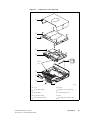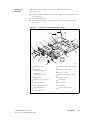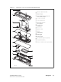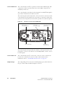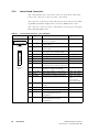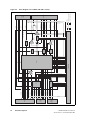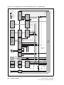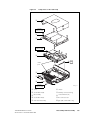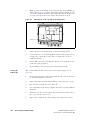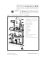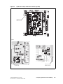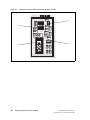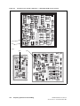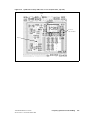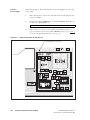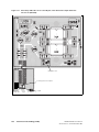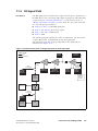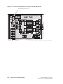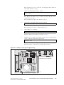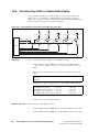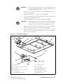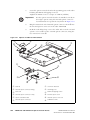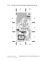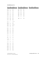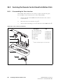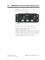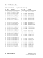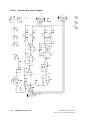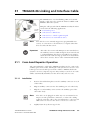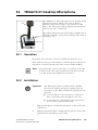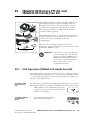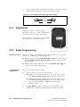
1
TM8100 mobiles
TM8200 mobiles
Service Manual
MMA-00005-05
Issue 5
November 2007
Contact Information
Intellectual Property Rights
Tait Radio Communications
Corporate Head Office
Tait Electronics Limited
P.O. Box 1645
Christchurch
New Zealand
For the address and telephone number of regional
offices, refer to the TaitWorld website:
Website: www.taitworld.com
This product may be protected by one or more patents
of Tait Electronics Limited together with their
international equivalents, pending patent applications
and registered trade marks: NZ338097, NZ508054,
NZ508340, NZ508806, NZ508807, NZ509242,
NZ509640, NZ509959, NZ510496, NZ511155,
NZ511421, NZ516280/519742, NZ519118,
NZ519344, NZ520650/537902, NZ522236,
NZ524369, NZ524378, NZ524509, NZ524537,
NZ524630, NZ530819, NZ534475, NZ534692,
NZ535471, NZ536945, NZ537434, NZ546295,
NZ547713, NZ521450, AU2003281447,
AU2002235062, AU2004216984, AU2005207405,
CA2439018, CA2554213, EU03784706.8,
EU02701829.0, EU04714053.8, EU05704655.9,
GB23865476, GB2386010, GB2413249,
GB0516092.4, US11,232716, US10/597339, US10/
520827, US10/468740, US5,745,840, US10/547653,
US10/546696, US10/547964, US10/523952, US11/
572700.
Technical Support
For assistance with specific technical issues, contact
Technical Support:
E-mail: [email protected]
Website: www.taitworld.com/technical
Copyright and Trademarks
All information contained in this document is the
property of Tait Electronics Limited. All rights reserved.
This document may not, in whole or in part, be copied,
photocopied, reproduced, translated, stored, or reduced
to any electronic medium or machine-readable form,
without prior written permission from Tait Electronics
Limited.
The word TAIT and the TAIT logo are trademarks of
Tait Electronics Limited.
All trade names referenced are the service mark,
trademark or registered trademark of the respective
manufacturers.
To Our European Customers
Tait Electronics Limited is an
environmentally responsible company
which supports waste minimization and
material recovery. The European Union’s
Waste Electrical and Electronic Equipment
Directive requires that this product be disposed of
separately from the general waste stream when its
service life is over. Please be environmentally
responsible and dispose through the original supplier,
your local municipal waste “separate collection” service,
or contact Tait Electronics Limited.
Disclaimer
There are no warranties extended or granted by this
document. Tait Electronics Limited accepts no
responsibility for damage arising from use of the
information contained in the document or of the
equipment and software it describes. It is the
responsibility of the user to ensure that use of such
information, equipment and software complies with the
laws, rules and regulations of the applicable
jurisdictions.
Enquiries and Comments
If you have any enquiries regarding this document, or
any comments, suggestions and notifications of errors,
please contact Technical Support.
Updates of Manual and Equipment
In the interests of improving the performance, reliability
or servicing of the equipment, Tait Electronics Limited
reserves the right to update the equipment or this
document or both without prior notice.
2
TM8100/TM8200 Service Manual
© Tait Electronics Limited November 2007
Contents
Preface . . . . . . . . . . . . . . . . . . . . . . . . . . . . . . . . . . . . . . . . . . . . . . . . . 5
Scope of Manual . . . . . . . . . . . . . . . . . . . . . . . . . . . . . . . . . . . . . . . . . . . . 5
Hardware and Software Versions . . . . . . . . . . . . . . . . . . . . . . . . . . . . . . . . 5
Associated Documentation. . . . . . . . . . . . . . . . . . . . . . . . . . . . . . . . . . . . . 6
Publication Record . . . . . . . . . . . . . . . . . . . . . . . . . . . . . . . . . . . . . . . . . . 7
Alert Notices . . . . . . . . . . . . . . . . . . . . . . . . . . . . . . . . . . . . . . . . . . . . . . 7
Abbreviations . . . . . . . . . . . . . . . . . . . . . . . . . . . . . . . . . . . . . . . . . . . . . . 8
Part A – Description of the Radio . . . . . . . . . . . . . . . . . . . . . . . . . . . . . . 11
1 Introduction. . . . . . . . . . . . . . . . . . . . . . . . . . . . . . . . . . . . . . . . . . . 13
2 Description . . . . . . . . . . . . . . . . . . . . . . . . . . . . . . . . . . . . . . . . . . . 21
3 Circuit Descriptions . . . . . . . . . . . . . . . . . . . . . . . . . . . . . . . . . . . . . 65
Part B – Servicing the Radio . . . . . . . . . . . . . . . . . . . . . . . . . . . . . . . . .103
4 General Information . . . . . . . . . . . . . . . . . . . . . . . . . . . . . . . . . . . . 107
5 Disassembly and Reassembly . . . . . . . . . . . . . . . . . . . . . . . . . . . . . . 135
6 Servicing Procedures . . . . . . . . . . . . . . . . . . . . . . . . . . . . . . . . . . . 155
7 Power Supply Fault Finding . . . . . . . . . . . . . . . . . . . . . . . . . . . . . . 169
8 Interface Fault Finding . . . . . . . . . . . . . . . . . . . . . . . . . . . . . . . . . . 179
9 Frequency Synthesizer Fault Finding . . . . . . . . . . . . . . . . . . . . . . . . 185
10 Receiver Fault Finding . . . . . . . . . . . . . . . . . . . . . . . . . . . . . . . . . . 247
11 Transmitter Fault Finding (>25W) . . . . . . . . . . . . . . . . . . . . . . . . . 267
12 Transmitter Fault Finding (25W) . . . . . . . . . . . . . . . . . . . . . . . . . . 341
13 CODEC and Audio Fault Finding. . . . . . . . . . . . . . . . . . . . . . . . . . 399
14 Fault Finding of Control Head with Graphical Display . . . . . . . . . . . 423
15 Fault Finding of Control Head with 1-, 2- or 3-Digit Display. . . . . . 447
16 Spare Parts . . . . . . . . . . . . . . . . . . . . . . . . . . . . . . . . . . . . . . . . . . . 455
Part C – Accessories . . . . . . . . . . . . . . . . . . . . . . . . . . . . . . . . . . . . . . .465
17 TMAA01-01 Line-Interface Board . . . . . . . . . . . . . . . . . . . . . . . . . 469
18 TMAA01-02 RS-232 Board . . . . . . . . . . . . . . . . . . . . . . . . . . . . . . 489
19 TMAA01-05 and TMAA01-07 Options Extender Boards . . . . . . . . 497
20 TMAA02-02 DTMF Microphone . . . . . . . . . . . . . . . . . . . . . . . . . 507
21 TMAA02-06 Support Kit for Concealed & Dynamic Microphones. . 511
22 TMAA02-07 Concealed Microphone . . . . . . . . . . . . . . . . . . . . . . . 519
23 TMAA02-08 Keypad Microphone . . . . . . . . . . . . . . . . . . . . . . . . . 521
24 TMAA03-02 Security Bracket . . . . . . . . . . . . . . . . . . . . . . . . . . . . 525
25 Installing a Remote Kit. . . . . . . . . . . . . . . . . . . . . . . . . . . . . . . . . . 529
26 Installing an Enhanced Remote Kit . . . . . . . . . . . . . . . . . . . . . . . . . 545
27 TMAA03-31 Control Head Interface Box . . . . . . . . . . . . . . . . . . . . 561
TM8100/TM8200 Service Manual
© Tait Electronics Limited November 2007
3
28
29
30
31
32
33
34
35
36
37
38
4
TMAA03-34 Extender Box . . . . . . . . . . . . . . . . . . . . . . . . . . . . . .
TMAA04-04 Crossband Linking Cable . . . . . . . . . . . . . . . . . . . . . .
TMAA04-05 Ignition Sense Kit . . . . . . . . . . . . . . . . . . . . . . . . . . .
TMAA04-06 Linking and Interface Cable . . . . . . . . . . . . . . . . . . . .
TMAA10-01 Desktop Microphone . . . . . . . . . . . . . . . . . . . . . . . .
TMAA10-02 Handset . . . . . . . . . . . . . . . . . . . . . . . . . . . . . . . . . .
TMAA10-03 and TMAA10-06 High-Power Remote Speakers . . . .
TMAA10-04 Remote PTT Kit and TMAA10-05 Hands-Free Kit . .
TMAA10-07 Desktop Microphone . . . . . . . . . . . . . . . . . . . . . . . .
TMAA10-08 Desktop Microphone . . . . . . . . . . . . . . . . . . . . . . . .
TOPA-SV-024 Test Unit. . . . . . . . . . . . . . . . . . . . . . . . . . . . . . . .
567
573
579
581
589
593
597
599
607
609
613
TM8100/TM8200 Service Manual
© Tait Electronics Limited November 2007
Preface
Scope of Manual
This manual contains information to service technicians for carrying out
level-1 and level-2 repairs of TM8100 and TM8200 radios and accessories.
Level-1 repairs entail the replacement of faulty parts and circuit boards;
level-2 repairs entail the repair of circuit boards, with the exception of
certain special items on the boards. The manual does not cover level-3
repairs, which entail the repair of the special items.
Hardware and Software Versions
This manual describes the following hardware and software versions.
The IPNs (internal part numbers) of the boards are listed below; the last two
digits in the IPN represent the issue of the board. The board information in
this manual covers all production-issue boards up to the issue listed below.
■
Main board (A4 band) 25W
: 220-02074-04
■
Main board (B1 band) 25W
: 220-01700-14
■
Main board (B1 band) 50W
: 220-01723-04
■
Main board (C0 band) 25W
: 220-01742-04
■
Main board (D1 band) 25W
: 220-01717-02
■
Main board (H5 and H6 bands) 25W
: 220-01697-11
■
Main board (K5 band) 30/35W
: 220-02146-06
■
Main board (G2, H5 and H7 bands) 40W
: 220-01722-04
■
Control-head board (1-digit display)
: 220-02070-01
■
Control-head board (2-digit display)
: 220-01699-03
■
Control-head board (3-digit display)
: 220-02151-02
■
Control-head board (graphical display)
: 220-01718-01
■
Control-head board (RJ45)
: 220-01720-05
■
Programming application (TM8100)
: version 3.02
■
Programming application (TM8200)
: version 4.02
■
Calibration application
: version 4.05
TM8100/TM8200 Service Manual
© Tait Electronics Limited November 2007
5
Associated Documentation
The following associated documentation is available for this product:
Manuals
■
■
■
■
■
■
PCB Information
■
■
■
■
■
■
■
■
■
■
■
■
■
■
■
■
MMA-00002-xx
MMA-00003-xx
MMA-00051-xx
MMA-00028-xx
MMA-00006-xx
MMA-00004-xx
TM8100 User’s Guide
TM8200 User’s Guide
TM8235 User’s Guide
TM8100/TM8200 Installation Guide
TM8100 Operator’s Guide
TM8200 Operator’s Guide
MMA-00016-xx TM8100/TM8200 Main Board A4 25W
MMAB12-B1-00-814TM8100/TM8200 Main Board B1 25W
(board IPN 220-01700-05)
MMA-00031-xx TM8100/TM8200 Main Board B1 25W
(boards after IPN 220-01700-05)
MMA-00050-xx TM8100/TM8200 Main Board C0 25 W
MMA-00032-xx TM8100/TM8200 Main Board D1 25W
MMAB12-H5-00-814TM8100/TM8200 Main Board H5/H6 25W
(board IPN 220-01697-05)
MMA-00033-xx TM8100/TM8200 Main Board H5/H6 25W
(boards after IPN 220-01697-05)
MMA-00069-xx TM8100/TM8200 Main Board K5 30/35W
MMA-00020-xx TM8100/TM8200 Main Board B1 50W
MMA-00021-xx TM8100/TM8200 Main Board G2/H5/H7 40W
MMA-00035-xx TM8100 Control-Head Board (2-Digit Display)
MMA-00036-xx TM8100 Control-Head Board (1-Digit Display)
MMA-00015-xx TM8200 Control-head Board (Graphical Display)
MMA-00058-xx TM8200 Control-Head Board (3-Digit Display)
MMA-00034-xx TM8200 Control-Head Board (RJ45)
MMA-00037-xx
TM8100/TM8200 PCB Information
(printed, pre-punched and shrink wrapped;
comprises the latest releases of MMA-00015-xx,
MMA-00016-xx, MMA-00020-xx, MMA-00021xx, MMA-00031-xx, MMA-00032-xx,
MMA-00033-xx, MMA-00034-xx, MMA-00035xx, MMA-00050-xx, MMA-00058-xx, MMA00069-xx).
The characters xx represent the issue number of the documentation.
All available documentation is provided on the
TM8100/TM8200 Service CD, product code TMAA20-01.
Updates may also be published on the Tait support website.
6
TM8100/TM8200 Service Manual
© Tait Electronics Limited November 2007
3DK Manuals
The following manuals are mainly of concern to third-party developers.
The manuals are supplied on the 3DK (third-party developer’s kit)
resource CD.
■
MMA-00011-xx
TM8100/TM8200 3DK Hardware Developer’s
Kit Application Manual
■
MMA-00014-xx
TMAA30-02 TM8000 3DK Application Board
Software Programmer’s Manual
■
MMA-00013-xx
TMAA30-02 TM8000 3DK Application Board
Service Manual
■
MMA-00038-xx
TM8100/TM8200 Computer-controlled Data
Interface Protocol Definition
Publication Record
Issue
Publication Date
Description
01
March 2005
first release
02
May 2005
update for 40W/50W radios
03
August 2005
update to board issue 10 (B1, H5 and H6 bands)
of 25W radios, incorporation of accessories
manual
04
June 2006
include TM8200 3-digit-display control head, A4
and C0 bands, and information on issue -05 main
board for B1, H5 and H6 bands
05
November 2007
include G2 and K5 bands,
update product codes of control heads,
new space frame and speaker clamp for control
heads with 1-, 2- or 3-digit display
Alert Notices
Within this manual, four types of alerts are given to the reader: warning,
caution, important and note. The following paragraphs illustrate each type
of alert and its associated symbol.
Warning!!
This alert is used when there is a potential risk
of death or serious injury.
Caution
This alert is used when there is the risk of minor or
moderate injury to people.
Important
This alert is used to warn about the risk of equipment damage or malfunction.
TM8100/TM8200 Service Manual
© Tait Electronics Limited November 2007
7
Note
This alert is used to highlight information that is required to
ensure that procedures are performed correctly.
Abbreviations
Abbreviation
8
Description
ACP
Adjacent Channel Power
ADC
Analog-to-Digital Converter
AGC
Automatic Gain Control
ALC
Automatic Level Control
ASC
Accredited Service Centre
C4FM
Compatible Four-level Frequency Modulation
CCTM
Computer-Controlled Test Mode
CODEC
Coder-Decoder
CSO
Customer Service Organisation
CTCSS
Continuous-Tone-Controlled Subaudible Signaling
DAC
Digital-to-Analog Converter
DC
Direct Current
DSP
Digital Signal Processor
DTMF
Dual-Tone Multi-Frequency
EPTT
External PTT (Press-To-Talk)
ESD
Electrostatic Discharge
FCL
Frequency Control Loop
FE
Front-End
FEC
Forward Error Correction
FPGA
Field-Programmable Gate Array
GPIO
General Purpose Input/Output
GPS
Global Positioning System
GUI
Graphical User Interface
IC
Integrated Circuit
IPN
Internal Part Number
IF
Intermediate Frequency
TM8100/TM8200 Service Manual
© Tait Electronics Limited November 2007
Abbreviation
Description
IQ
In-Phase and Quadrature
ISC
International Service Centre
LCD
Liquid-Crystal Display
LED
Light-Emitting Diode
LNA
Low-Noise Amplifier
LO
Local Oscillator
LPF
Low-Pass Filter
NPN
Negative-Positive-Negative
PA
Power Amplifier
PCB
Printed Circuit Board
PLL
Phase-Locked Loop
PNP
Positive-Negative-Positive
PSU
Power Supply Unit
PTT
Press-To-Talk
RISC
Reduced Instruction Set Computing
RSSI
Received Signal Strength Indication
SFE
Software Feature Enabler
SMA
Sub Miniature Version A
SMD
Surface-Mount Device
SMT
Surface-Mount Technology
SMPS
Switch-Mode Power Supply
SPI
Serial Peripheral Interface
TCXO
Temperature-Compensated Crystal Oscillator
TEL
Tait Electronics Limited
UHF
Ultra High Frequency
VCO
Voltage-Controlled Oscillator
VCXO
Voltage-Controlled Crystal Oscillator
VHF
Very High Frequency
TM8100/TM8200 Service Manual
© Tait Electronics Limited November 2007
9
10
TM8100/TM8200 Service Manual
© Tait Electronics Limited November 2007
Part A – Description of the Radio
1
Introduction . . . . . . . . . . . . . . . . . . . . . . . . . . . . . . . . . . . . . . . . . . 13
1.1 Frequency Bands . . . . . . . . . . . . . . . . . . . . . . . . . . . . . . . . . . . . . . . . . . 15
1.2 RF Output Power. . . . . . . . . . . . . . . . . . . . . . . . . . . . . . . . . . . . . . . . . 15
1.3 Accessories . . . . . . . . . . . . . . . . . . . . . . . . . . . . . . . . . . . . . . . . . . . . . . 16
1.4 Product Codes . . . . . . . . . . . . . . . . . . . . . . . . . . . . . . . . . . . . . . . . . . . 17
1.5 Labels . . . . . . . . . . . . . . . . . . . . . . . . . . . . . . . . . . . . . . . . . . . . . . . . . . 19
1.6 Specifications . . . . . . . . . . . . . . . . . . . . . . . . . . . . . . . . . . . . . . . . . . . . 19
2
Description . . . . . . . . . . . . . . . . . . . . . . . . . . . . . . . . . . . . . . . . . . . 21
2.1 Mechanical Design . . . . . . . . . . . . . . . . . . . . . . . . . . . . . . . . . . . . . . . . 21
2.2 User Interfaces . . . . . . . . . . . . . . . . . . . . . . . . . . . . . . . . . . . . . . . . . . . 37
2.3 Connectors . . . . . . . . . . . . . . . . . . . . . . . . . . . . . . . . . . . . . . . . . . . . . . 38
2.4 Hardware and Software Architecture . . . . . . . . . . . . . . . . . . . . . . . . . . . 47
2.5 Operation in Receive Mode . . . . . . . . . . . . . . . . . . . . . . . . . . . . . . . . . 52
2.6 Operation in Transmit Mode . . . . . . . . . . . . . . . . . . . . . . . . . . . . . . . . . 57
3
Circuit
3.1
3.2
3.3
3.4
3.5
3.6
3.7
3.8
3.9
3.10
3.11
Descriptions . . . . . . . . . . . . . . . . . . . . . . . . . . . . . . . . . . . . . 65
Transmitter Circuitry . . . . . . . . . . . . . . . . . . . . . . . . . . . . . . . . . . . . . . 67
Receiver Circuitry . . . . . . . . . . . . . . . . . . . . . . . . . . . . . . . . . . . . . . . . 70
Frequency Synthesizer Circuitry. . . . . . . . . . . . . . . . . . . . . . . . . . . . . . . 75
Frequency Control Loop . . . . . . . . . . . . . . . . . . . . . . . . . . . . . . . . . . . . 80
CODEC and Audio Circuitry . . . . . . . . . . . . . . . . . . . . . . . . . . . . . . . . 81
Power Supply Circuitry . . . . . . . . . . . . . . . . . . . . . . . . . . . . . . . . . . . . . 85
Interface Circuitry . . . . . . . . . . . . . . . . . . . . . . . . . . . . . . . . . . . . . . . . . 90
Digital Board . . . . . . . . . . . . . . . . . . . . . . . . . . . . . . . . . . . . . . . . . . . . 93
Control-Head Board with Graphical Display . . . . . . . . . . . . . . . . . . . . . 96
Control-Head Board with 1-, 2- or 3-Digit Display . . . . . . . . . . . . . . . . 99
RJ45 Control Head. . . . . . . . . . . . . . . . . . . . . . . . . . . . . . . . . . . . . . . 102
TM8100/TM8200 Service Manual
© Tait Electronics Limited November 2007
11
12
TM8100/TM8200 Service Manual
© Tait Electronics Limited November 2007
1
Introduction
The TM8100 and TM8200 series is a range of high-performance
microprocessor-controlled radios for analog voice and data communication.
The radios are designed for installation in vehicles but can also be used in
desktop, remote-monitoring and similar applications.
This manual includes the information required for servicing the radio and
its accessories.
This section describes the different options available for:
■ frequency bands
■ RF output power
■ accessories
■ product codes.
This section also gives an overview of the labels on the product and the
specifications.
Figure 1.1
TM8200 mobile radios
TM8235 radio with 3-digit-display control head
TM8250 or TM8255 radio with graphical-display control head
TM8252 radio with RJ45 control head
TM8100/TM8200 Service Manual
© Tait Electronics Limited November 2007
Introduction
13
Figure 1.2
TM8100 mobile radios
TM8115 radio with 2-digit-display control head
TM8110 radio with 1-digit-display control head
TM8105 radio with blank control head
rear view (25W radio)
14
Introduction
TM8100/TM8200 Service Manual
© Tait Electronics Limited November 2007
1.1
Frequency Bands
The radios are available in the following frequency bands:
■
66 to 88MHz (A4)
■
136 to 174MHz (B1)
■
174 to 225MHz (C0)
■
216 to 266MHz (D1)
■
350 to 400MHz (G2)
■
400 to 470MHz (H5)
■
450 to 530MHz (H6)
■
450 to 520MHz (H7)
■
762 to 870MHz (K5 Tx)
762 to 776MHz and 850 to 870MHz (K5 Rx)
The frequency bands are implemented by different main boards in the radio
body. The control heads are identical for all frequency bands.
1.2
RF Output Power
The radio bodies are available with >25W and 25W RF output power.
The two RF output power options are implemented by different main
boards in the radio body, mechanically different radio bodies, and different
power connectors. The control heads are identical for all RF output
power options.
The >25W radio is available in the following frequency bands:
>25W
■
B1 (50W)
■
G2 (40W)
■
H5 (40W)
■
H7 (40W)
■
K5 (35W/30W)
The 25W radio is available in the following frequency bands:
25W
■
A4
■
B1
■
C0
■
D1
■
H5
■
H6
TM8100/TM8200 Service Manual
© Tait Electronics Limited November 2007
Introduction
15
1.3
Accessories
Tait offers a large variety of audio accessories, installation kits, internal
options boards and other accessories such as a desktop power supply.
For more information on these accessories refer to “Part C – Accessories”
on page 465.
Audio Accessories
Installation Kits
The radios allow for the connection of a comprehensive range of audio
accessories:
■
rugged microphone (standard)
■
DTMF microphone
■
keypad microphone
■
handset
■
concealed microphone (TM8200) and concealed microphone kit
(TM8100)
■
high-power remote speaker
■
remote PTT kit and hands-free kit.
The radio is delivered with a vehicle installation kit, including a U-bracket.
Installation of the radio is described in the user’s guide or the installation
guide.
Optional installation kits are:
Internal Options
Boards
■
remote control-head kit for remote installation of the control head
■
security bracket for secure and quick-release installation
■
ignition-sense kit.
The radio provides space for an internal options board inside the radio body
connecting to an internal options connector. An aperture for an external
options connector is also provided.
Tait offers the following internal options boards:
■
line-interface board
■
RS-232 board
■
options-extender board.
Control-Head
Options Boards
The radio provides space for a control-head options board inside the blank
control head of the TM8105 and TM8252 radios.
Desktop Power
Supply
A desktop power supply including the parts for mounting the radio is
available for desktop installations.
16
Introduction
TM8100/TM8200 Service Manual
© Tait Electronics Limited November 2007
1.4
Product Codes
This section describes the product codes used to identify products of the
TM8100 and TM8200 mobile radio product lines.
General
The product codes of the TM8100 and TM8200 mobile radio product lines
have the format:
TMAabc–ddee
where:
Radio Bodies
■
a identifies the product category:
A=accessory, B=radio body, C=control head, S=software feature
■
b, c, dd and ee identify specific product features.
The product codes of the radio bodies have the format:
TMABbc–ddee[f]
where:
Control Heads
■
b identifies the architecture of the digital board:
1=conventional analog
2=conventional analog (dual-mode capability)
3 identifies the digital boards of the digital TM9100 product line.
■
c identifies the RF output power:
2=25W, 3=25W (trigger-base), 4=30 to 59W,
5=30 to 59W (trigger-base).
■
dd identifies the frequency band:
A4=66 to 88MHz, B1=136 to 174MHz, C0=174 to 225MHz,
D1=216 to 266MHz, G2 =350 to 400MHz, H5=400 to 470MHz,
H6=450 to 530MHz, H7=450 to 520MHz, K5=762 to 870MHz
(Tx), 762 to 776MHz and 850 to 870MHz (Rx).
■
ee identifies any radio options:
00=BNC RF connector, 01=mini-UHF RF connector
■
[f] (optional) identifies a combination of software features as loaded at
the time of manufacture
The product code of the control heads has the format:
TMACbc–dd[ee]
where:
■
bc identifies control-head user interface and hardware options
■
dd identifies badging and configuration variants
■
[ee] (optional) identifies variations from the standard firmware and or
data load at the time of manufacture.
TM8100/TM8200 Service Manual
© Tait Electronics Limited November 2007
Introduction
17
bc:
Control-head user interface and
hardware options
dd
10
blank control head, no display, 9-pin Drange connector
0T Tait, TM8105
0A Auriga
20
2-digit-display control head
0T Tait, TM8115
OE ECG, TM8115
AT Tait, Auriga (dual badge)
30
RJ45 control head, two RJ45 connectors
0T
Tait, TM8252
31
RJ45 control head for multi-body, two
RJ45 connectors, RS485
0T
1T
Tait, TM8200
Tait, TM8200, termination
resistor in
Tait, TM8200, termination
resistor out
2T
32
RJ45 control head, two RJ45 connectors,
customer-specific product
0T
Tait, TM8124
34
RJ45 control head for dual-head, two
RJ45 connectors, RS485
0T
Tait, TM8200
40
graphical-display control head
0T
0E
1T
2T
Tait, TM8200
ECG, TM8200
Tait, TM8200, yellow
Tait, TM8200, green
42
graphical-display control head
1T
2T
Tait, TM8200, yellow
Tait, TM8200, green
50
1-digit-display control head
0T
AT
Tait, TM8110
Tait, Auriga (dual badge)
60
3-digit-display control head
0T
Tait TM8235
Note
18
Introduction
Badging and
configuration variants
Product codes not listed here identify control-head configurations
of the digital TM9100 product line.
TM8100/TM8200 Service Manual
© Tait Electronics Limited November 2007
1.5
Labels
Four external labels are attached to the bottom of the radio body:
■
compliance information
■
serial number and product code
■
hot surface safety warning
■
RF exposure safety warning.
1.6
TMAH6C
TAIT
Made in
New Zealand
Figure 1.3
Labels of the TM8100 and TM8200 product lines
N46
IC: 737A-TMAH6C
FCC ID: CASTMAH6C
Contains intellectual property licenced
by Digital Voice Systems Inc, Motorola
Inc and Tait Electronics Ltd.
Details in user documentation.
S/N 19061964
TMAB22-H600
450-530 MHz
Tait Electronics Ltd, NZ
Specifications
For up-to-date specifications, refer to the area on the TaitWorld website
reserved for TM8100 and TM8200 products.
TM8100/TM8200 Service Manual
© Tait Electronics Limited November 2007
Introduction
19
20
Introduction
TM8100/TM8200 Service Manual
© Tait Electronics Limited November 2007
2
Description
This section describes the mechanical design and architecture of the radio,
explains the operation of the transceiver and the control head, and gives
pinouts of the radio connectors.
2.1
Overview
Mechanical Design
The radio consists of the following main components:
■
control head B
■
radio body C.
Figure 2.1
Components of the radio
C
B
D
E
3068z_01
The control head B clips firmly to the front face of the radio body C,
where a seal E provides IP54 class protection. A control-head loom D
connects the control head to the radio body. Two dot-dash-dot marks at the
bottom of the radio body indicate the positions where a screwdriver is
applied to separate the control head from the radio body.
TM8100/TM8200 Service Manual
© Tait Electronics Limited November 2007
Description
21
2.1.1
Radio Body
The radio body consists of the following main components (see Figure 2.2
on page 23):
Overview
■
cover B
■
lid D
■
internal options board (optional)
■
chassis G
■
main-board assembly F.
Cover
The black plastic cover B wraps over the top and sides of the radio body.
Apertures in the sides of the cover allow access to the four external screw
bosses of the radio body used for mounting the radio to the U-bracket.
Lid
The aluminium lid D is attached to the chassis G with four M4x16 Torxhead screws C. A seal fitted inside a groove at the underside of the lid
provides for IP54 class protection. The rear of the lid has an aperture for an
external options connector, which may be fitted if an internal options board
is used. If no external options connector is used, the aperture is sealed with
a bung for IP54 class protection. The lid contains two of the four screw
bosses to attach the radio to the U-bracket of the installation kit.
Internal Options
Board (Optional)
On the inside of the lid, nine screw points are provided for mounting an
internal options board, which can be sized and shaped as required.
The internal options board connects to the internal options connector of
the main board. Tait offers a range of internal options board, which are
described in the accessories section of this manual. For more information on
how to create your own internal options board, contact Tait Electronics
Limited.
Chassis
The aluminium chassis g is different for the >25W radio and the 25W
radio.
>25W
25W
The chassis G houses the main-board assembly F, which is attached with
five screws E to screw bosses inside the chassis and with two screws I
through the rear of the chassis to the heat-transfer block.
The rear of the chassis has apertures for the RF, power and auxiliary
connectors of the main board. If the auxiliary connector is not used, the
aperture is sealed with a rubber bung J for IP54 class protection.
The RF connector has a rubber seal H which is fitted inside the aperture
for the RF connector.
22
Description
TM8100/TM8200 Service Manual
© Tait Electronics Limited November 2007
Figure 2.2
Components of the radio body
B
Cx4
D
Ex5
F
1)
>25W
thermal
paste
G
H
Ix2
J
3630z_01
B
C
D
E
F
cover
screw M4x16 (x4)
lid assembly
screw M3x10 (x5)
main-board assembly
TM8100/TM8200 Service Manual
© Tait Electronics Limited November 2007
G
H
I
J
1)
chassis
auxiliary connector bung
screws M4x16 (x2)
seal
gap pad (>25W radio only)
Description
23
The front of the chassis has an aperture for the control-head connector.
The control-head seal is fitted inside a groove around the flange at the front
face of the chassis and provides for IP54 class protection when the control
head is fitted. Two dot-dash-dot marks at the underside side of the chassis
indicate the leverage points for removing the control head from the
radio body.
The sides of the chassis contain two of the four screw bosses to attach the
radio to the U-bracket of the installation kit.
For heat dissipation, the chassis has heat fins at the rear, grooves at the
bottom, and holes in the front.
>25W
25W
>25W
24
Description
The heat fins at the rear of the >25W radio are longer than those of the
25W radio. The grooves at the bottom of the >25W radio are deeper than
those of the 25W radio.
For additional heat dissipation, the >25W radio has an additional L-shaped
gap pad 1) between the chassis and the main board.
TM8100/TM8200 Service Manual
© Tait Electronics Limited November 2007
Main-Board
Assembly
The main-board assembly consists of the following components
(see Figure 2.3):
■
main board 1^ with SMT components, digital board D, shielding cans,
and connectors
■
heat-transfer block H
■
mounting and sealing elements for the connectors at the rear of the
radio body.
Figure 2.3
Components of the main-board assembly
Cx2
E
Bx3
D
1&
F
G
H
I
1!
1@
1^
1%
J
1)
thermal
paste
>25W
1$
1#
B
C
M3x10 screw (x3)
>25W radios:
M2.2x10 PT screw (x2)
25W radios:
K30x8 PT screw (x2)
D
E
F
G
H
I
digital board
internal options connector
auxiliary connector
inner foam D-range seal
heat-transfer block
3631z_01
J
1)
1!
1@
1#
1$
1%
1^
1&
D-range screwlock fastener (x2)
power connector seal
power connector
gap pad (>25W radio only)
hexagonal nut
lock washer
RF connector
main board
control-head connector
outer foam seal
TM8100/TM8200 Service Manual
© Tait Electronics Limited November 2007
Description
25
The main board 1^ is attached to the heat-transfer block H with three
M3x10 Torx-head screws B and the fastening elements J, 1# and 1$ of the
auxiliary and RF connectors.
The inner foam D-range seal G seals the auxiliary connector against the
heat-transfer block. The power connector seal 1) seals the power connector
against the heat-transfer block.
>25W
25W
The power connector seal 1) of the >25W radio (blue) is different to the
seal of the 25W radio (black).
The main board 1^ is a printed circuit board in SMT design with
components on the top and bottom sides. A digital board D is reflowsoldered to the main board. Most components are shielded by metal cans.
Main Board
There are different main boards for each frequency band and each RF
output power configuration.
The internal options connector E for connecting an internal options board
and the factory connector (not illustrated) for factory use are soldered to the
top side of the main board. The control-head connector 1& (facing the front
of the radio) and the auxiliary F, power 1! and RF 1% connectors (facing
the rear of the radio) are located on the bottom side of the main board.
>25W
25W
The >25W radio has a black power connector 1! and the 25W radio has a
white power connector.
For more information on the connectors, refer to “Connectors” on
page 38.
For heat dissipation, one of the screw bosses inside the chassis is in contact
with the underside of the main board. A larger copper plate at the underside
of the main board connects to the body of the heat-transfer block.
>25W
Heat-Transfer Block
The >25W radio has an additional gap pad between the heat-transfer block
and the main board 1^ which connects to an additional copper plate at the
bottom side of the main board.
The aluminium heat-transfer block H dissipates heat from the main board
to the heat fins of the chassis. The heat-transfer block has a contact surface
to the larger copper plate at the underside of the main board 1^, and a
contact surface to the rear of the chassis. All contact surfaces are coated with
thermal paste.
Two self-adhesive foam seals G and I around the aperture of the auxiliary
connector on either side of the heat-transfer block and the power connector
seal 1) inside the aperture of the power connector are fitted to the heattransfer block.
26
Description
TM8100/TM8200 Service Manual
© Tait Electronics Limited November 2007
2.1.2
Control Head with Graphical Display
Overview
The control head can be divided into the following main areas:
■
front panel with control elements, indicators, LCD, speaker, and
concealed microphone (optional)
■
space frame and seals
■
control-head board with SMT components, shielding cans, connectors,
and volume potentiometer
■
control-head loom with female-female adapter
■
adapter flange.
The circled numbers in this section refer to the items in Figure 2.4 on
page 29.
Front Panel
Assembly
The front panel assembly 1^ consists of an injection-moulded plastic part
with an integrated transparent light pipe element for the radio STATUS LEDs,
a transparent lens which cannot be replaced, a cloth membrane which is
fixed to the speaker grille, and a foam seal inside a rectangular LCD recess
behind the lens. A label 1* with the radio model number is attached to the
front panel assembly with self-adhesive coating and can be replaced for
rebranding purposes.
Three clips on the rear side of the front panel assembly snap onto the space
frame to hold the keypads 1# and 1#, the LCD assembly 1@ and the speaker
1! in place. The rear side of the front panel assembly also has four screw
bosses to fasten the control-head board F.
Knob for
Volume-Control
Potentiometer
The knob for the volume-control potentiometer 1& is fitted to the shaft of
the volume-control potentiometer, which is soldered to the control-head
board F.
Keypads
The main keypad 1# (for the function, selection, and scroll keys) and the
power keypad 1$ protrude through apertures in the front panel assembly 1^.
The rear sides of these keypads connect directly to the relevant contacts on
the control-head board F.
LCD Assembly
The graphical-display LCD assembly 1@ sits on a foam seal inside a
rectangular recess of the front panel assembly 1^. Another foam seal is
attached to the rear of the LCD with self-adhesive coating. The LCD
assembly has a loom, which runs through a slot in the space frame J and
connects to a connector on the rear side of the control-head board F.
TM8100/TM8200 Service Manual
© Tait Electronics Limited November 2007
Description
27
Speaker
The speaker 1! sits inside a round recess of the front panel assembly, where
a cloth membrane is fixed to the speaker grille. The speaker clamp 1) holds
the speaker in position. The speaker cable plugs into the speaker connector
on the rear side of the control-head board F.
Note
In some configurations the speaker may be disconnected.
Concealed
Microphone
(Optional)
A concealed microphone 1% consisting of the microphone capsule and a
rubber seal can be fitted in a round recess inside the front panel assembly 1^.
The microphone leads are soldered to two pads on the top side of the
control-head board. Before the microphone is fitted, a small hole is drilled
in the recess to provide an acoustic path to the microphone. The hole is
covered by the rubber seal to ensure that the control head remains sealed to
IP54 standards. For more information refer to “TMAA02-07 Concealed
Microphone” on page 519.
Space Frame
The aluminium space frame J snaps into the three clips of the front panel
assembly 1^. The front side of the space frame holds the keypads, the LCD
assembly, and the speaker in place and at the same time allows access to their
electrical contacts. The rear side of the space frame has four through-holes
for the screws E of the control-head board F and two screw bosses to fit
the adapter flange C. Two light pipes H and I are fitted in recesses in the
space frame and direct light from LEDs on the control-head board to the
front panel. A slot at the top edge of the space frame allows the loom of the
LCD assembly 1@ to run to the control-head board.
Seals
Two identical ring seals G fitted to grooves around the perimeter of the
space frame provide for IP54 class protection.
28
Description
TM8100/TM8200 Service Manual
© Tait Electronics Limited November 2007
Figure 2.4
Components of the control head with graphical display
Bx2
C
D
Ex4
F
G
H
I
J
G
B
C
M4 x 12 Taptite screw (x2)
D
control-head loom assembly with
female-female adapter
E
F
G
H
I
J
1)
1!
1@
1#
1$
1%
1^
1&
3 x 10 PT screw (x4)
adapter flange
control-head board
space frame seal (x2)
short light pipe
long light pipe
space frame
speaker clamp
speaker
LCD assembly
main keypad
power keypad
concealed microphone (optional)
front panel assembly
knob for volume-control potentiometer
1)
1!
1@
1%
1#
1$
1^
3451z_02
TM8100/TM8200 Service Manual
© Tait Electronics Limited November 2007
1&
Description
29
Control-Head Board
The control-head board F is a printed circuit board in SMT design with
components on the top and bottom sides. Some SMT components are
shielded by metal cans.
The control-head board is fitted to the front panel assembly 1^ through the
space frame J with four 3x10 PT screws E.
The side facing the radio body has the connectors for the connection of the
control-head loom, the LCD loom, the speaker, an optional control-head
options board, and pads for the leads of the optional concealed microphone.
Figure 2.5
Connectors of the control-head board
pads for leads of
concealed microphone
connector for speaker
connector for
loom of LCD assembly
connector for control-head
options board
connector for
control-head loom
The side facing the front panel has the volume-control potentiometer, the
microphone connector, the indicator and backlight LEDs, and the contacts
for the keypads.
Control-Head Loom
The control-head loom D connects the connector on the control-head
board to the control-head connector of the radio body. For more
information refer to “Control-Head Connectors” on page 44.
Adapter Flange
The adapter flange C is an injection-moulded plastic part, which is fitted to
the space frame with two M4x12 Taptite screws B.
30
Description
TM8100/TM8200 Service Manual
© Tait Electronics Limited November 2007
2.1.3
Control Heads with 1-, 2- or 3-Digit Display
Overview
The control heads with 1-, 2- or 3-digit display can be divided into the
following main areas:
■
front panel with control elements, indicators, speaker, and optional
concealed microphone
■
space frame
■
control-head board with SMT components, shielding cans, connectors,
and volume potentiometer
■
control-head loom with female-female adapter.
The circled numbers in this section refer to the items in Figure 2.6 on
page 33.
Front Panel
Assembly
The front panel assembly H consists of an injection-moulded plastic part
with an integrated transparent light pipe element for the radio STATUS LEDs,
a transparent lens which cannot be replaced, and a cloth membrane which
is fixed to the speaker grille. Depending on the type of control head, the
aperture on the lens is sized to display either one, two or three characters.
A label with the radio model number is attached to the front panel assembly
with self-adhesive coating and can be replaced for rebranding purposes.
Six clips on the space frame G snap into corresponding locations on the
inside of the front panel assembly to hold the keypad 1!, the LCD 1@, the
speaker clamp1 h, and the speaker i in place.
Knob for
Volume-Control
Potentiometer
The knob for the volume-control potentiometer 1% is fitted to the shaft of
the volume-control potentiometer, which is soldered to the control-head
board F.
Keypad
The keypad 1! protrudes through apertures in the front panel assembly H.
The rear side of each key connects directly to the relevant contact on the
control-head board E. Four light pipes j and 1) are fitted in the
appropriate recesses in the keypad and direct light from LEDs on the
control-head board to the front panel.
LCD
The LCD 1@ sits inside a rectangular recess of the front panel assembly 1$
and is held in place by the space frame G. Electrical contact between the
LCD and the control-head board is ensured by two elastomeric strips F
held in place by the space frame.
1. The speaker clamp h and a new space frame g were introduced in
April 2007.
TM8100/TM8200 Service Manual
© Tait Electronics Limited November 2007
Description
31
Speaker
The speaker I sits inside a round recess of the front panel assembly, where
a cloth membrane is fixed to the speaker grille. The space frame g and
the speaker clamp h hold the speaker in position. The speaker cable plugs
into the speaker connector on the rear side of the control-head board E.
Note
In some configurations the speaker may be disconnected.
Concealed
Microphone
(Optional)
A concealed microphone 1# consisting of the microphone capsule and a
rubber seal can be fitted in a round recess inside the front panel assembly 1$.
The microphone leads are soldered to two pads on the top side of the
control-head board E. Before the microphone is fitted a small hole is drilled
in the recess to provide an acoustic path to the microphone. The hole is
covered by the rubber seal to ensure that the control head remains sealed to
IP54 standards. For more information refer to “TMAA02-06 Support Kit
for Concealed and Dynamic Microphones” on page 511.
Space Frame
The plastic space frame G clips into the six recesses inside the front panel
assembly 1$. The front side of the space frame holds the keypad (with the
four light pipes), the LCD, the speaker clamp1, and the speaker in place and
at the same time allows access to their electrical contacts. The rear side of
the space frame has three holes for the screws D of the control-head board
E.
Control-Head Board
The control-head board E is a printed circuit board in SMT design with
components on the top and bottom sides. There are different boards for the
control heads with 1-, 2- and 3-digit display.s
The control-head board is clipped and then fitted to the space frame G with
three 3x8 PT screws D.
The side facing the radio body has the connectors for the connection of the
control-head loom B, the speaker, an optional control-head options board
C, and pads for the leads of the optional concealed microphone 1#.
The side facing the front panel has the volume-control potentiometer, the
microphone connector, the indicator and backlight LEDs, the contacts for
the keypads, and the LCD.
Control-Head Loom
32
Description
The control-head loom B with the female-female adapter connects the
connector on the control-head board E to the control-head connector of
the radio body. For more information refer to “Control-Head Connectors”
on page 44.
TM8100/TM8200 Service Manual
© Tait Electronics Limited November 2007
Figure 2.6
Components of the control head (1-, 2- or 3-digit display)
B
C
dx3
E
Fx2
g
j
h
1)
1!
B
control-head loom with female-female
adapter
C
D
E
F
G
H
I
J
1)
1!
1@
1#
1$
1%
control-head options board (optional)
3 x 8 PT screw (x3)
control-head board
elastomeric strip (x2)
space frame
speaker clamp
speaker
short light pipe
long light pipe
keypad
LCD
concealed microphone (optional)
front panel assembly
knob for volume-control potentiometer
i
1#
1@
1$
1%
TM8100/TM8200 Service Manual
© Tait Electronics Limited November 2007
Description
33
2.1.4
RJ45 Control Head
The RJ45 control head consists of the following parts:
■
front panel
■
control-head loom with female-female adaptor
■
control-head board
■
PCB bracket.
The circled numbers in this section refer to the items in Figure 2.7 on
page 35.
Front Panel
The front panel F is an injection-moulded plastic part with two apertures
for the fitted programming connector and a second optional RJ45
connector. When not in use, the apertures are sealed with two RJ45 bungs
F to ensure that the control head is sealed to IP54 standards. There is also a
hole for the POWER ON/OFF LED which illuminates through the label.
A label with the model number is attached to the front panel with selfadhesive coating and can be replaced for rebranding purposes.
The rear side of the front panel has four screw bosses to fasten the PCB
bracket E.
Control-Head Loom
The control-head loom C with the female-female adapter connects the
connector on the control-head board B to the control-head connector of
the radio body. For more information refer to “Control-Head Connectors”
on page 44.
Control-Head Board
The control-head board B is a printed circuit board in SMT design with
some hand-soldered parts.
All components are placed on the top side, including the programming
connector, the connector for the control-head loom C, and the
POWER ON/OFF LED.
The control-head board slides into a slot in the front panel and slots in the
PCB bracket E, and is held in place by two clips of the PCB bracket E.
PCB Bracket
34
Description
The PCB bracket E is an injection-moulded plastic part which is fitted to
the front panel F with four 3x8 PT screws D.
TM8100/TM8200 Service Manual
© Tait Electronics Limited November 2007
Figure 2.7
Components of the RJ45 control head
B
C
Dx4
E
F
G x2
B
C
D
control-head board
control-head loom with female-female adapter
3 x 8 PT screw (x4)
TM8100/TM8200 Service Manual
© Tait Electronics Limited November 2007
E
F
G
PCB bracket
front panel
RJ45 bung (x2)
Description
35
2.1.5
Blank Control Head
The blank control head consists of the following parts:
■
front panel
■
control-head loom with programming connector
■
seals.
The circled numbers in this section refer to the items in Figure 2.8 on
page 36.
Front Panel
The front panel E is an injection-moulded plastic part with an aperture for
fitting the programming connector, which is part of the control-head loom
G. A label with the model number is attached to the front panel with selfadhesive coating and can be replaced for rebranding purposes.
Control-Head Loom
The programming connector at one end of the control-head loom and a
foam seal F are screwed to the front panel with a pair of lock-nuts D.
When the programming connector is not in use, the seal C is fitted with
two screws B to ensure that the control head is sealed to IP54 standards.
The control-head loom with the female-female adapter connects to the
control-head connector of the radio body. For more information refer to
“Control-Head Connectors” on page 44.
There is provision in the blank control head for the fitting of a custom circuit
board.
Figure 2.8
Components of the blank control head
x2
B
G
C
x2 D
F
3/16 inch (5mm)
4lb·in (0.45N·m)
E
3829z_01
B
C
D
36
UNX 4-40 x 3/16-inch pan Pozi screw (x2)
cover seal
lock-nut (pair)
Description
E
F
G
front panel
foam seal
control-head loom with female-female adapter
TM8100/TM8200 Service Manual
© Tait Electronics Limited November 2007
2.2
User Interfaces
Figure 2.9 shows the controls and indicators of the user interfaces. For more
information refer to the following user’s guides:
■
TM8100 (1-digit and 2-digit-display control head)
■
TM8250/TM8255 (graphical-display control head)
■
TM8235 (3-digit-display control head).
Some keys have functions assigned to both short and long key presses.
A short key press is less than one second, and a long key press is more than
one second.
Figure 2.9
User interfaces
press-to-talk
(PTT) key
radio status LEDs
microphone
green
red amber
speaker
display
on/off key
volume
control
microphone
socket
function keys
1 to 4
scroll keys
left
selection key
right
selection key
display
radio status LEDs
green
speaker
red amber
on/off key
volume
control
microphone
socket
1- and 2-digit-display
control head:
function keys 1to 4
3-digit-display
control head: function key 1
TM8100/TM8200 Service Manual
© Tait Electronics Limited November 2007
scroll keys
clear key
shift key function key 2
Description
37
2.3
Connectors
This section describes the specifications and pinouts of the connectors of the
radio body and the control head.
Overview
Figure 2.10 provides an overview of the connectors:
Figure 2.10
Connectors (radio with graphical-display control head)
Volume
Control
Control-Head
Options Connector
RF Connector
Microphone
Connector
Control-Head
Options Board
Control-Head
Loom
Keys
Control-Head
Connector
Control-Head
Board
Main Board
Internal
Options
Connector
Power
Connector
LCD
LEDs
Internal
Options
Loom
Pads for
Concealed
Microphone
Speaker
Connector
Factory
Connector
(Factory Only)
Speaker
Auxiliary
Connector
Internal
Options
Board
External
Options
Connector
Speaker
Leads
Figure 2.11 shows the connectors of the radio body.
Figure 2.12 shows the connectors of the control head.
For information on the factory connector of the main board and the internal
connectors of the control head, refer to the PCB information of the main
boards and the control-head board.
38
Description
TM8100/TM8200 Service Manual
© Tait Electronics Limited November 2007
Figure 2.11
Connectors of the radio body (25W radio)
front view
control-head
connector
provision for
external options
connector
provision for
additional
connector
rear view
auxiliary
connector
power
connector
RF
connector
internal options
connector
top view
TM8100/TM8200 Service Manual
© Tait Electronics Limited November 2007
Description
39
Figure 2.12
Connectors of the control head with graphical display
front view
microphone
connector
control-head
connector
rear view without adapter flange
Figure 2.13
Connectors of the control head with 1-, 2- or 3-digit display
microphone
connector
front view
connector for speaker
control-head
connector
rear view
pads for leads of
concealed microphone
40
Description
connectors for
optional circuit board
TM8100/TM8200 Service Manual
© Tait Electronics Limited November 2007
2.3.1
RF Connector
The RF connector is the primary RF interface to the antenna. The RF
connector is a BNC connector or a mini-UHF connector with an
impedance of 50Ω.
Important
Table 2.1
The maximum RF input level is +27dBm. Higher levels
may damage the radio.
RF connector - pins and signals
Pinout
Pin
B
1
RF
RF analog
2
GND
RF ground
Power Connector
>25W
25W
The power connector is the interface for the primary 13.8V power source
and the external speaker. The primary power source can be the vehicle
battery or a mains-fed DC power supply. There are different power
connectors for the >25W and 25W radios.
Important
Table 2.2
The speaker load configuration is balanced; the speaker
output lines must not be connected to ground. Connecting
a speaker output line to ground will cause audio power
amplifier shutdown
Power connector (radio) – pins and signals
Pinout
Pin
Signal name
rear view
3
4
Signal type
AGND
Earth return for radio body power
source.
Ground
2
SPK–
External speaker output. Balanced load
configuration.
Analog
3
SPK+
External speaker output. Balanced load
configuration.
Analog
4
13V8_BATT
DC power input for radio body and
control head.
Power
25W radio
2
Description
1
>25W radio
1
Signal Type
C
rear view
2.3.2
Signal Name
rear view
TM8100/TM8200 Service Manual
© Tait Electronics Limited November 2007
Description
41
2.3.3
Auxiliary Connector
The auxiliary connector is the standard interface for external devices that are
typically connected to a radio. The auxiliary connector is a 15-way
standard-density D-range socket. The auxiliary connector provides a serial
port, three programmable input lines, four programmable digital I/O lines
and audio I/O.
The I/O lines can be programmed for a variety of functions, logic levels,
and in some cases, direction. Audio lines can also be programmed to tap
into, or out of, different points in the audio processing chain. For more
information refer to the online help of the programming application.
Table 2.3
Auxiliary connector – pins and signals
Pinout
Pin
B
C
D
E
F
G
H
I
J
1)
1!
1@
1#
1$
1%
rear view
Signal name
Description
Signal type
12
AUX_GPI1
General purpose digital input.
Programmable function.
Digital, 3V3 CMOS
5
AUX_GPI2
General purpose digital input.
Programmable function.
With LK3 fitted, GPI2 is an
emergency power sense input.a
Digital, 3V3 CMOS
4
AUX_GPI3
General purpose digital input.
Programmable function.
With LK2 fitted, GPI3 is a power
sense input.a
Digital, 3V3 CMOS
10
AUX_GPIO4
2
AUX_GPIO5
9
AUX_GPIO6
Programmable function and
direction.
Pads available to fit a higher power
driver transistor on GPIO4 line
Digital, 3V3 CMOS
input; open collector
output with pullup
1
AUX_GPIO7
11
AUX_TXD
Asynchronous serial port Transmit data
Digital, 3V3 CMOS
3
AUX_RXD
Asynchronous serial port Receive data
Digital, 3V3 CMOS
7
AUD_TAP_IN
Programmable tap point into the Rx
or Tx audio chain. DC-coupled.
Analog
13
AUD_TAP_OUT
Programmable tap point out of the
Rx or Tx audio chain. DC-coupled.
Analog
14
AUX_MIC_AUD Auxiliary microphone input.
Electret microphone biasing
provided. Dynamic microphones are
not supported.
Analog
6
RSSI
Analog RSSI output.
Analog
8
+13V8_SWb
Switched 13.8V supply. Supply is
switched off when radio body is
switched off.
Power
15
AGND
Analog ground
Ground
a. For more information on hardware links refer to “Power-Sense Options” on page 85.
b. Can be switched or unswitched. For more information refer to “Connector Power Supply Options” on page 90.
42
Description
TM8100/TM8200 Service Manual
© Tait Electronics Limited November 2007
2.3.4
Internal Options Connector
When installing an internal options board, the internal options connector is
the electrical interface to the main board of the radio body.
The internal options connector provides similar I/O to the auxiliary
connector. The internal options connector is an 18-pin 0.1 inch pitch
Micro-MaTch connector.
Important
Table 2.4
The digital I/O signals are intended to interface directly
with compatible logic signals only. Do not connect these
signals to external devices without appropriate signal conditioning and ESD protection.
Internal options connector – pins and signals
Pinout
Pin
CB
ED
GF
IH
1)J
1@1!
1$1#
1^1%
1*1&
top view
Signal
Description
Signal type
1
13V8_SWa
Switched 13V8 supply. Supply is switched Power
off when the Radio Body is switched off.
2
AUD_TAP_OUT
Programmable tap point out of the Rx or
Tx audio chain. DC-coupled.
Analog
3
AGND
Analog ground.
Ground
4
AUX_MIC_AUD Auxiliary microphone input.
Analog
Electret microphone biasing provided.
Dynamic microphones are not supported.
5
RX_BEEP_IN
Receive sidetone input. AC-coupled.
6
AUD_TAP_IN
Programmable tap point into the Rx or Tx Analog
audio chain. DC-coupled.
7
RX_AUD
Receive audio output. Post volume
control. AC-coupled.
Analog
8
RSSI
Analog RSSI output.
Analog
9…15 IOP_GPIO1…7
Analog
General-purpose port for input and
Digital.
output of data. Programmable function
3V3 CMOS
and direction. With LK4 fitted, GPIO7 is a
power sense inputb.
16
DGND
Digital ground.
Ground
17
IOP_RXD
Asynchronous serial port - Receive data.
Digital.
3V3 CMOS
18
IOP_TXD
Asynchronous serial port - Transmit data.
Digital.
3V3 CMOS
a. Can be switched or unswitched. For more information refer to “Connector Power Supply Options” on page 90.
b. For more information on hardware links refer to“Power-Sense Options” on page 85.
2.3.5
Provision for External Options Connector
The radio has a mechanical interface for the external connector of an
internal options board. This external options connector can be a 9-way
standard-density or 15-way high-density D-range connector. If no internal
options board is installed (standard configuration), the hole for the external
options connector is sealed by a bung.
TM8100/TM8200 Service Manual
© Tait Electronics Limited November 2007
Description
43
2.3.6
Control-Head Connectors
The control-head loom connects the connector on the front of the radio
body to the connector on the rear of the control head.
The connector on the front of the radio body is an 18-way two-row rightangled IDC (insulation displacement connector) SMD header socket.
The connector on the rear of the control head is an 18-way 0.1 inch pitch
Micro-MaTch SMD socket.
Table 2.5
Control-head connectors – pins and signals
Pinout
Pin
Signal
1
RX_AUD
Analog
CEGI1)1@1$1^1*
BDFHJ1!1#1%1&
Receive audio output. Post volume
control. AC-coupled.
2
+13V8a
Power
front view
of radio body
Power supply output from radio body
power source.
3
CH_TXD
Asynchronous serial port Transmit data.
Digital. 3V3 CMOS.
4
CH_PTT
PTT input from microphone.
Also carries the hookswitch signal.
Digital
5
CH_MIC_AUD Fist microphone audio input.
Analog
6
AGND
Analog ground.
Ground
7
CH_RXD
Asynchronous serial port - Receive data. Digital. 3V3 CMOS.
8
DGND
Digital ground.
Ground
9
CH_ON_OFF
Hardware power on/softwarecontrolled power off input. Active low.
Digital
10
VOL_WIP_DC
DC signal from volume pot wiper
(grounded for graphical display).
Analog
11
CH_SPI_DO
Data output signal to control head.
Digital. 3V3 CMOS.
12
CH_LE
Latch enable output to control head.
Digital. 3V3 CMOS.
13
CH_GPIO1
General purpose digital input/output.
Digital. 3V3 CMOS
input.
Open collector
output with pullup.
14
+3V3
Power supply to control head digital
circuits.
Power
15
CH_SPI_DI
Data input from control head.
Digital. 3V3 CMOS.
16
CH_SPI_CLK
Clock output to control head.
Digital. 3V3 CMOS.
17
SPK–
Speaker audio output for non-remote
control head. Balanced load
configuration.
Analog
18
SPK+
Speaker audio output for non-remote
control head. Balanced load
configuration.
Analog
CB
ED
GF
IH
1)J
1@1!
1$1#
1^1%
1*1&
top view of
control-head
board
Description
Signal type
a. Can be switched or unswitched. For more information refer to “Connector Power Supply Options” on page 90.
44
Description
TM8100/TM8200 Service Manual
© Tait Electronics Limited November 2007
2.3.7
Microphone Connector
The microphone connector of the control head is an RJ45 socket.
When the control head is connected to the control-head connector of the
radio body using the loom provided, the microphone connector uses the
following eight control-head connector signals:
Table 2.6
Microphone connector – pins and signals
Pinout
Pin
Signal name
Description
Signal type
1
MIC_RX_AUD Receive audio output.
Analog
B
2
+13V8a
Power supply output. Switched off
when radio body is switched off.
Power
I
3
MIC_TXD
Asynchronous serial port Transmit data.
3.3V CMOS
4
MIC_PTT
PTT input from microphone. Also carries Digital
hookswitch signal.
5
MIC_AUD
Fist microphone audio input.
Analog
6
AGND
Analog ground.
Analog ground
7
MIC_RXD
Asynchronous serial port - Receive data. 3.3V CMOS
8
MIC_GPIO1
General purpose digital input/output.
front view
Open collector out
3.3V CMOS in
a. Can be switched or unswitched. For more information refer to “Connector Power Supply Options” on page 90.
2.3.8
Programming Connector (RJ45 Control Head)
The programming connector of the RJ45 control head is an RJ45 socket.
When the RJ45 control head is connected to the radio body, the
programming connector uses the following signals.
Table 2.7
Programming connector – pins and signals
Pinout
Pin
I
Signal name
Signal type
1
PRG_RX_AUD
Receive audio output.
Analog
2
+13V8a
Power supply output. Switched off
when radio body is switched off.
Power
3
PRG_TXD
Asynchronous serial port Transmit data.
3.3V CMOS
4
PRG_PTT
PTT input from microphone.
Also carries hookswitch signal.
Digital
B
front view
Description
5
PRG_MIC_AUD
Fist microphone audio input.
Analog
6
AGND
Analog ground
Ground
7
PRG_RXD
Asynchronous serial port Receive data.
3.3V CMOS
8
PRG_ON_OFF
Hardware power on/software-power Digital
off input. Active low.
a. Can be switched or unswitched. For more information refer to “Connector Power Supply Options” on page 90.
TM8100/TM8200 Service Manual
© Tait Electronics Limited November 2007
Description
45
2.3.9
Programming Connector (Blank Control Head)
The programming connector of the blank control head is a 9-way standarddensity D-range plug.
When the blank control head is connected to the radio body, the
programming connector uses the following signals.
Table 2.8
Programming connector – pins and signals
Pinout
front view
Pin
Signal name
Description
Signal type
1
PRG_RX_AUD
Receive audio output.
Analog
2
PRG_TXD
Asynchronous serial port Transmit data.
3.3V CMOS
3
PRG_MIC_AUD
Fist microphone audio input.
Analog
4
PRG_RXD
Asynchronous serial port Receive data.
3.3V CMOS
5
PRG_ON_OFF
Hardware power on/software-power Digital
off input. Active low.
6
+13V8a
Power supply output. Switched off
when radio body is switched off.
Power
7
PRG_PTT
PTT input from microphone.
Also carries hookswitch signal.
Digital
8
AGND
Analog ground
Ground
9
DGND
Digital ground
Ground
a. Can be switched or unswitched. For more information refer to “Connector Power Supply Options” on page 90.
46
Description
TM8100/TM8200 Service Manual
© Tait Electronics Limited November 2007
2.4
Hardware and Software Architecture
This section describes the hardware and software modules of the radio and
their interaction in the functioning of the radio.
Overview
2.4.1
Hardware Architecture
The electrical hardware of the radio is implemented on a main board inside
the radio body and a control-head board inside the control head.
For a detailed description and block diagrams of individual circuits, refer to
“Circuit Descriptions” on page 21.
Main Board
The main board inside the radio body includes the following circuitry:
■
transmitter
■
receiver
■
frequency synthesizer
■
digital board with a RISC processor and custom logic (implemented on
an FPGA), memory, and a DSP
■
CODEC and audio
■
interface
■
power supply.
The main board has an internal options connector which allows internal
options boards to access a variety of discrete and programmable signals.
For more information refer to “Internal Options Connector” on page 43.
For a basic block diagram of the main board, refer to Figure 2.14 on
page 48.
For a more detailed block diagram of the transceiver, refer to Figure 2.16 on
page 53.
Control-Head Board
The control-head board of the control head with graphical display includes:
■
the circuitry needed for the controls and indicators on the front panel
■
with a RISC processor and custom logic (implemented on an FPGA),
and memory.
For a block diagram of this control-head board, refer to Figure 3.15 on
page 97.
The control head with graphical display may have a concealed microphone
inside the control head and also has provision for a separate circuit board that
may be designed to perform a variety of tasks including—but not limited
to—Bluetooth connectivity. No separate circuit board is required for a
dynamic microphone.
TM8100/TM8200 Service Manual
© Tait Electronics Limited November 2007
Description
47
RF Connector
48
Description
Receiver
part of transmitter circuitry
part of CODEC and audio circuitry
2)
2)
digital-to-analog converter
1)
2)
Transmitter
PIN
Switch1)
analog-to-digital converter
LPF
1)
Main Board
RF
analog
digital
asynchronous serial data
synchronous serial data
Frequency
Synthesizer
Custom
Logic
RISC
Proc.
FPGA
DSP
Flash
Memory
SRAM
Serial
Flash
Digital Board
Power Supply
CODEC
and Audio
Interface
Internal Options
Connector
Auxiliary
Connector
Control-Head
Connector
Power
Connector
Figure 2.14
Hardware architecture of the main board
TM8100/TM8200 Service Manual
© Tait Electronics Limited November 2007
2.4.2
Software Architecture
Overview
Software plays an important role in the functioning of the radio. Some radio
functions such as the graphical user interface, processing of the analog and
digital signals, and the implementation of radio applications are completely
implemented by software.
For a block diagram of the software architecture, refer to Figure 2.15 on
page 50.
Software Modules
The following software modules are stored on the digital board of the main
board:
■
FPGA image, which includes the software-implemented RISC processor
and the custom logic (the custom logic executes additional digital signal
processing)
■
boot code
■
radio application code
■
digital signal processing
■
radio application database and radio calibration database.
The following software modules are stored on the control-head board with
graphical display:
■
FPGA image, which includes the software-implemented RISC processor
■
boot code
■
control-head application code
■
control-head application database.
Hardware and interface drivers are part of the boot code, the RISC code,
and—in the case of the main board—the DSP code.
TM8100/TM8200 Service Manual
© Tait Electronics Limited November 2007
Description
49
Database
Flash
Memory
Boot Code
Serial
Flash
Application Code
Software architecture (radio with graphical-display control head shown)
FPGA Image
Figure 2.15
FPGA
Serial Flash
FPGA Image
FPGA Image
RISC Processor
Flash Memory
Control-Head Application Code
Boot Code
Boot Code
Radio Application
Code
Boot Code
Radio Application Code
Database
DSP Code
Custom Logic
DSP
DSP Code
Additional Digital
Signal Processing
RISC Proc.
SRAM
FPGA Image
SRAM
FPGA
Dynamic Memory
Dynamic
Memory
Software Start-Up
When the radio is turned on, the following processes are carried out on the
main board:
Note
50
Description
This process describes the software start-up into normal radio
operation mode.
1.
The FPGA image, which includes the RISC processor and the custom logic, is loaded from the serial flash to the FPGA.
2.
The RISC processor executes the boot code, which carries out an
initialization and auto-calibration, and—in the case of a fault—
generates an error code for display on the control head.
3.
Normal radio operation starts with:
■
the RISC processor executing the radio application code,
including application software
■
the DSP executing the DSP code for processing of digital signals
■
the custom logic executing additional digital signal processing.
TM8100/TM8200 Service Manual
© Tait Electronics Limited November 2007
When the radio is turned on, the following processes are carried out on the
control-head board of the control head with graphical display:
1.
The FPGA image, which includes the RISC processor, is loaded from
the serial flash to the FPGA.
2.
The RISC processor executes the boot code, which carries out an
initialization, and—in the case of a fault—generates an error code for
display on the control head.
3.
Normal radio operation starts with the RISC processor executing
■
the graphical user interface
■
the I/O processing
■
the user interface processing.
During normal radio operation the radio body and control head
communicate via interface software, which is part of the radio and controlhead application software.
Software Shutdown
On shutdown, the programming and calibration data is stored in the
database, and power is removed from the radio.
Important
On power loss, any changes made to the programming or
calibration data may be lost.
Programming and
Calibration Files
One of the servicing tasks is the downloading and uploading of
programming and calibration files to the database. For more information,
refer to “Servicing Procedures” on page 155 and the online help of the
programming and calibration applications.
Software Upgrades
During servicing it may become necessary to upload software to a
replacement main board, control head, or control head board using the
Tools > > Download command of the programming application. For more
information, refer to the online help of the programming application and to
the technical notes accompanying the software files.
TM8100/TM8200 Service Manual
© Tait Electronics Limited November 2007
Description
51
2.5
Operation in Receive Mode
Overview
This section describes the functioning of the transceiver in receive mode.
The operation of the transceiver is illustrated in Figure 2.16 on page 53. For
the K5 front end, refer to
These block diagrams show the hardware modules integrated with the
software modules:
■
hardware (transmitter, receiver, CODEC and audio)
■
RISC processor (on FPGA of digital board)
■
custom logic (on FPGA of digital board)
■
DSP (on digital board).
The receive path consists of three major functional parts:
52
Description
■
RF hardware
■
digital baseband processing
■
audio processing and signalling.
TM8100/TM8200 Service Manual
© Tait Electronics Limited November 2007
Figure 2.16
Transceiver operation
TM8100/TM8200 Service Manual
© Tait Electronics Limited November 2007
Description
53
2.5.1
RF Hardware
PIN Switch
The RF PIN switch circuitry selects the RF path to and from the antenna
to either the Tx or Rx circuitry of the radio. In addition to the switching
functionality, the PIN switch is used to provide attenuation to the Rx front
end in high signal-strength locations.
Front End and
First IF
The front-end hardware amplifies and image-filters the received RF
spectrum, then down-converts the desired channel frequency to a first
intermediate frequency (IF1) of 21.4MHz (VHF) or 45.1MHz (UHF and
K5 band) where coarse channel filtering is performed. The first LO signal is
obtained from the frequency synthesizer and is injected on the low side of
the desired channel frequency for all bands. In receive mode, the modulation
to the frequency synthesizer is muted. See “Frequency Synthesizer” on
page 59 for a description of the frequency synthesizer. The output of the
first IF is then down-converted using an image-reject mixer to a low IF of
64kHz. The K5 front-end has two paths (762 to 776MHz and 850 to
870MHz) which are selected depending on the Rx frequency.
Quadrature
Demodulator
The LO for the image-reject mixer (quadrature demodulator) is synthesized
and uses the TCXO as a reference. This ensures good centring of the IF
filters and more consistent group-delay performance. The quadrature
demodulator device has an internal frequency division of 2 so the second
LO operates at 2 x (IF1+64kHz). The quadrature output from this mixer is
fed to a pair of ADCs with high dynamic range where it is oversampled at
256kHz and fed to the custom logic device.
Automatic Gain
Control
The AGC is used to limit the maximum signal level applied to the imagereject mixer and ADCs in order to meet the requirements for
intermodulation and selectivity performance. Hardware gain control is
performed by a variable gain amplifier within the quadrature demodulator
device driven by a 10-bit DAC. Information about the signal level is
obtained from the IQ data output stream from the ADCs. The control loop
is completed within the custom logic. The AGC will begin to reduce gain
when the combined signal power of the wanted signal and first adjacent
channels is greater than about -70dBm. In the presence of a strong adjacentchannel signal it is therefore possible that the AGC may start acting when
the wanted signal is well below -70dBm.
Noise Blanking
(A4, B1 bands only)
With frequency bands between 66 and 174MHz, a noise blanker can be
selected to remove common sources of electrical interference such as vehicle
ignition noise. The noise blanker functions by sampling the RF input to the
receiver for impulse noise and momentarily disconnecting the first LO for
the duration of the impulse. The response time of the noise blanker is very
fast (tens of nanoseconds) and is quicker than the time taken for the RF
signal to pass through the front-end hardware, so that the LO is disabled
before the impulse reaches the IF stage where it could cause crystal
filter ring.
54
Description
TM8100/TM8200 Service Manual
© Tait Electronics Limited November 2007
2.5.2
Digital Baseband Processing
Custom Logic
The remainder of the receiver processing up to demodulation is performed
by custom logic. The digitized quadrature signal from the RF hardware is
digitally down-converted to a zero IF and channel filtering is performed at
baseband. Different filter shapes are possible to accommodate the various
channel spacings and data requirements. These filters provide the bulk of
adjacent channel selectivity for narrow-band operation. The filters have
linear phase response so that good group-delay performance for data is
achieved. The filters also decimate the sample rate down to 48kHz.
Custom logic also performs demodulation, which is multiplexed along with
AGC and amplitude data and fed via a single synchronous serial port to the
DSP. The stream is demultiplexed and the demodulation data used as an
input for further audio processing.
Noise Squelch
The noise squelch process resides in the DSP. The noise content above and
adjacent to the voice band is measured and compared with a preset
threshold. When a wanted signal is present, out-of-band noise content is
reduced and, if below the preset threshold, is indicated as a valid wanted
signal.
RSSI
Receive signal strength is measured by a process resident in the DSP.
This process obtains its input from the demodulator (RF signal magnitude
value) and from the AGC (present gain value). With these two inputs and a
calibration factor, the RF signal strength at the antenna can be accurately
calculated.
Calibration
The following items within the receiver path are factory-calibrated:
■
front-end tuning
■
AGC
■
noise squelch
■
RSSI.
Information on the calibration of these items is given in the on-line help
facility of the calibration application.
TM8100/TM8200 Service Manual
© Tait Electronics Limited November 2007
Description
55
2.5.3
Audio Processing and Signalling
Audio Processing
Raw demodulated data from the receiver is processed within the DSP.
The sample rate at this point is 48kHz with signal bandwidth limited only
by the IF filtering. Scaling (dependent on the bandwidth of the RF channel)
is then applied to normalize the signal level for the remaining audio
processing. The sample rate is decimated to 8kHz and 0.3 to 3kHz bandpass
audio filtering is applied. De-emphasis is then applied to cancel out the
receive signals pre-emphasized response and improve signal to noise
performance. Optional processing such as decryption or companding is then
applied if applicable.
Data and Signalling
Decoders
The data and signalling decoders obtain their signals from various points
within the audio processing chain. The point used depends on the decoders’
bandwidth and whether de-emphasis is required. Several decoders may be
active simultaneously.
Side Tones
Side tones are summed in at the end of the audio processing chain. These are
tones that provide some form of alert or give the user confidence an action
has been performed. The confidence tones may be generated in receive or
transmit mode. The sidetone level is a fixed proportion (in the order of
-10dB) relative to full scale in the receive path.
CODEC
The combined audio and side-tone signal is converted to analog form by a
16-bit DAC with integral anti-alias filtering. This is followed by a
programmable-gain amplifier with 45dB range in 1.5dB steps, that performs
primary volume control and muting. The DAC and primary volume control
are part of the same CODEC device (AD6521).
Output to Speakers
The output of the CODEC is fed to an audio power amplifier via a
secondary volume control (not TM8100 radios) and to the control head via
a buffer amplifier. The output configuration of the audio power amplifier is
balanced and drives an internal speaker in non-remote control-head
configuration and, optionally, an external speaker. The speaker loads are
connected in parallel rather than being switched. The power delivered to
each speaker is limited by its impedance. The internal speaker has 16Ω
impedance whereas the external speaker can be as low as 4Ω.
Volume Control
Configurations
There are two volume controls in the TM8200 radio but only one is active
at any time when audio is being output to the speaker(s). The inactive
volume control is set to maximum. For non-remote control-head
configuration, the primary volume control is active. For remote controlhead configuration, the secondary volume control is active. This enables
fixed level audio feed to the remote control head, and independent volume
control of the external speaker and the speaker of the remote control head.
56
Description
TM8100/TM8200 Service Manual
© Tait Electronics Limited November 2007
2.6
Overview
Operation in Transmit Mode
This section describes the functioning of the transceiver in transmit mode.
The operation of the transceiver is illustrated in Figure 2.16 on page 53.
These block diagrams show the hardware modules integrated with the
software modules:
■
hardware (transmitter, receiver, CODEC and audio)
■
RISC processor (on FPGA of digital board)
■
custom logic (on FPGA of digital board)
■
DSP block (on digital board).
The transmit path consists of three major functional parts:
■
audio processing and signalling
■
frequency synthesizer
■
RF transmitter.
TM8100/TM8200 Service Manual
© Tait Electronics Limited November 2007
Description
57
2.6.1
Audio Processing and Signalling
Microphone Input
The input to the transmitter path begins at the microphone input. There are
two microphone sources: a fist microphone connected to the control head
and an auxiliary microphone connected via the auxiliary or external options
connector. Only electret-type microphones are supported. Support for
optional dynamic fist microphones is facilitated by a hardware amplifier and
filter in the control head, and must be activated in the programming
software.
Analog Processing
of the Microphone
Input
The CODEC (AD6521) performs microphone selection and amplification.
The microphone amplifier consists of a fixed gain amplifier of 16dB
followed by a programmable-gain amplifier with 0 to 22dB gain.
The amplified microphone signal is converted to a digital stream by a 16-bit
ADC with integral anti-alias filtering (0.1 to 3.2kHz). The digital stream is
transported to the DSP for further audio processing.
Automatic Level
Control
The ALC follows and is used to effectively increase dynamic range by
boosting the gain of the microphone pre-amplifier under quiet conditions
and reducing the gain under noisy acoustic conditions. The ALC function
resides in the DSP and controls the microphone-programmable gain
amplifier in the CODEC. The ALC has a fast-attack (about 10ms) and
slow-decay (up to 2s) gain characteristic. This characteristic ensures that the
peak signal level is regulated near full scale to maximize dynamic range.
DSP Audio
Processing
The output of the automatic level control provides the input to the DSP
audio processing chain at a sample rate of 8kHz. Optional processing such
as encryption or companding is done first if applicable. Pre-emphasis, if
required, is then applied. The pre-emphasized signal is hard limited to
prevent overdeviation and filtered to remove high frequency components.
The sample rate is then interpolated up to 48kHz and scaled to be suitable
for the frequency synthesizer.
Data and Signalling
Encoders
The data and signalling encoders inject their signals into various points
within the audio processing chain. The injection point depends on the
encoders bandwidth and whether pre-emphasis is required.
58
Description
TM8100/TM8200 Service Manual
© Tait Electronics Limited November 2007
2.6.2
Frequency Synthesizer
Introduction
Frequency Control
Loop
As shown in Figure 2.16, the frequency synthesizer consists of two main
parts:
■
FCL (frequency control loop)
■
RF PLL, comprising RF PLL device, loop filter, VCO, and VCO output
switch.
The FCL consists of the following:
■
TCXO
■
mixer
■
loop filter
■
VCXO
■
frequency control block.
The FCL provides the reference frequency for the RF PLL. The FCL
generates a high-stability reference frequency that can be both modulated
and offset in fine resolution steps.
RF PLL
The RF PLL consists of the following:
■
RF PLL device
■
loop filter
■
VCO
■
VCO output switch.
The RF PLL has fast-locking capability but coarse frequency resolution.
This combination of control loops creates improved frequency generation
and acquisition capabilities.
Note that patents are pending for several aspects of the synthesizer design.
Operation of
Control Loop
The RF PLL is a conventional integer-N-type design with frequency
resolution of 25kHz (30kHz for the 66 to 88MHz A4 band). In transmit
mode, the loop locks to the transmit frequency. In receive mode, it locks to
the receive frequency minus the first IF frequency, except for the A4 band,
where it locks to the receive frequency plus the first IF frequency.
In the 762 to 870MHz K5 band, there are two VCOs. In transmit mode,
the loop locks to the transmit frequency. In receive mode, it locks to the
receive frequency plus the first IF frequency when the receiver is operating
in the lower sub-band (762 to 776MHz), and it locks to the receive
frequency minus the first IF frequency when the receiver is operating in the
upper sub-band (850 to 870MHz).
Initially, the VCO generates an unregulated frequency in the required range.
This is fed to the PLL device (ADF4111) and divided down by a
programmed ratio to approximately 25kHz. For the receive VCO in the K5
TM8100/TM8200 Service Manual
© Tait Electronics Limited November 2007
Description
59
band, the frequency is divided down to 72kHz. This is because the
sensitivity (KVCO = 4MHz/V) is four times lower than that of the
transmit VCO.
The reference frequency input from the FCL is also divided down to
approximately 25kHz (30kHz for the A4 band, 72kHz receive for the
K5 band). The phase of the two signals is compared and the error translated
into a DC voltage by a programmable charge pump and dual-bandwidth
loop filter. This DC signal is used to control the VCO frequency and reduce
the initial error. The loop eventually settles to a point that minimizes the
phase error between divided down reference and VCO frequencies. The net
result is that the loop “locks” to a programmed multiple of the reference
frequency.
The FCL generates an output of 13.012MHz±4kHz. Initially, a VCXO
(voltage controlled crystal oscillator) produces a quasi-regulated frequency in
the required range. The VCXO output is fed to a mixer where it is mixed
with the 13.000MHz TCXO frequency. The mixer, after low-pass filtering
to remove unwanted products, produces a frequency of 12kHz nominally.
This is converted to digital form and transported to the frequency control
block in the custom logic.
The frequency control block compares the mixer output frequency to a
reference generated by the digital clock and creates a DC error signal.
A programmed offset is also added. This error signal is converted to analog
form and used to control the VCXO frequency and reduce the initial error.
Once settled, the loop “locks” to the TCXO frequency with a programmed
offset frequency. The FCL output therefore acquires the TCXO's
frequency stability.
Modulation
The full bandwidth modulation signal is obtained from the DSP in digital
form at a sample rate of 48kHz. In traditional dual-point modulation
systems the modulation is applied, in analog form, to both the frequency
reference and the VCO in the RF PLL, combining to produce a flat
modulation response down to DC. Reference modulation is usually applied
directly to the TCXO.
In the system employed in the radio, the frequency reference is generated by
the FCL, which itself requires dual-point modulation injection to allow
modulation down to DC. With another modulation point required in the
RF PLL, this system therefore requires triple-point modulation.
The modulation signals applied to the FCL are in digital form while for the
RF PLL (VCO) the modulation signal is applied in analog form.
The modulation cross-over points occur at approximately 30 and 300Hz as
determined by the closed loop bandwidths of the FCL and RF PLL
respectively.
Frequency
Generation
60
Description
The RF PLL has a frequency resolution of 25kHz (30kHz for the A4 band,
72kHz receive for the K5 band). Higher resolution cannot be achieved
owing to acquisition-time requirements and so for any given frequency the
error could be as high as ±12.5kHz. This error is corrected by altering the
TM8100/TM8200 Service Manual
© Tait Electronics Limited November 2007
reference frequency to the RF PLL. The FCL supplies the reference
frequency and is able to adjust it up to ±300ppm with better than 0.1ppm
resolution (equivalent to better than 50Hz resolution at the RF frequency).
The FCL offset will usually be different for receive and transmit modes.
Fast Frequency
Settling
Both the FCL and RF PLL employ frequency-acquisition speed-up
techniques to achieve fast frequency settling. The frequency-acquisition
process of the FCL and RF PLL is able to occur concurrently with minimal
loop interaction owing to the very large difference in frequency step size
between the loops.
Frequency
Acquisition of
RF PLL
In the RF PLL the loop bandwidth is initially set to high by increasing the
charge-pump current and reducing time constants in the loop filter.
As a result, settling to within 1kHz of the final value occurs in under 4ms.
In order to meet noise performance requirements the loop parameters are
then switched to reduce the loop bandwidth. There is a small frequency kick
as the loop bandwidth is reduced. Total settling time is under 4.5ms.
Frequency
Acquisition of FCL
The FCL utilizes self-calibration techniques that enable it to rapidly settle
close to the final value while the loop is open. The loop is then closed and
settling to the final value occurs with an associated reduction in noise.
The total settling time is typically less than 4ms.
Calibration
The following items are calibrated in the frequency synthesizer:
■
nominal frequency
■
KVCO
■
KVCXO
■
VCO deviation.
Calibration of the nominal frequency is achieved by adding a fixed offset to
the FCL nominal frequency; the TCXO frequency itself is not adjusted.
The items KVCO and KVCXO are the control sensitivities of the RF VCO
(in MHz/V) and VCXO (in kHz/V) respectively. The latter has
temperature compensation.
TM8100/TM8200 Service Manual
© Tait Electronics Limited November 2007
Description
61
2.6.3
RF Transmitter
RF Power Amplifier
and Switching
(>25W Radio)
>25W
The RF power amplifier and exciter of the 40W/50W radio is a five-stage
line-up with approximately 40dB of power gain. The output of the
frequency synthesizer is first buffered to reduce kick during power ramping.
The buffer output goes to a discrete exciter that produces approximately 300
to 400mW output. This is followed by an LDMOS driver producing up to
8W output that is power-controlled. The final stage consists of two parallel
LDMOS devices producing enough power to provide 40 to 50W at
the antenna.
The RF power amplifier and exciter of the 30W/35W K5 band radio is a
four-stage line-up with approximately 38dB of power gain. The output of
the frequency synthesizer is first buffered to reduce kick during power
ramping. The buffer output goes to a discrete exciter that produces
approximately 500mW output. This is followed by an LDMOS driver
producing up to 6W output. The final stage consists of two parallel
LDMOS devices producing enough power to provide 30W at 762 to
806MHz and 35W at 806 to 870MHz at the antenna.
RF Power Amplifier
and Switching
(25W Radio)
25W
The RF power amplifier of the 25W radio is a four-stage line-up with
approximately 37dB of power gain. The output of the frequency synthesizer
is first buffered to reduce kick during power ramping. The buffer output
goes to a broad-band exciter IC that produces approximately 200mW
output. This is followed by an LDMOS driver producing up to 2W output
that is power-controlled. The final stage consists of two parallel LDMOS
devices producing enough power to provide 25W at the antenna.
Output of RF Power
Amplifier
The output of the RF power amplifier passes through a dual-directional
coupler, used for power control and monitoring, to the PIN switch.
The PIN switch toggles the antenna path between the receiver and
transmitter in receive and transmit modes respectively. Finally, the output is
low-pass-filtered to bring harmonic levels within specification.
Power Control
The steady-state power output of the transmitter is regulated using a
hardware control loop.
>25W
25W
62
Description
With the 40/50W radios and 30/35W K5 band radios, the sum of the
forward power output from the RF power amplifier and reverse power
reflected from the load is sensed by the directional coupler and fed back to
the power control loop.
With the 25W radios, the forward power output from the RF power
amplifier is sensed by the directional coupler and fed back to the power
control loop. The PA output power is controlled by varying driver gate bias
voltage that has a calibrated maximum limit to prevent overdrive. The power
control signal is supplied by a 13-bit DAC driven by custom logic.
TM8100/TM8200 Service Manual
© Tait Electronics Limited November 2007
Power ramp-up consists of two stages:
Ramping
■
bias
■
power ramping.
The timing between these two stages is critical to achieving the correct
overall wave shape in order to meet the specification for transient ACP
(adjacent channel power). A typical ramping waveform is shown in
Figure 2.17.
Figure 2.17
Typical ramping waveforms
Power
Bias Power
ramp ramp
Power Bias
ramp ramp
High power
Low power
Time
The steady-state final-stage bias level is supplied by an 8-bit DAC
programmed prior to ramp-up but held to zero by a switch on the DAC
output under the control of a TX INHIBIT signal. Bias ramp-up begins upon
release by the TX INHIBIT signal with the ramping shape being determined by
a low-pass filter. Owing to power leakage through the PA chain, ramping
the bias takes the PA output power from
Bias Ramp-Up
>25W
25W
■
less than –20dBm for the 40/50W radios
■
–20dBm to approximately 40dB below steady-state power for the
30/35W K5 band radios
■
–10dBm to approximately 25dB below steady-state power for the 25W
radios.
Power Ramp-Up
The power ramp signal is supplied by a 13-bit DAC that is controlled by
custom logic. The ramp is generated using a look-up table in custom logic
memory that is played back at the correct rate to the DAC to produce the
desired waveform. The ramp-up and ramp-down waveforms are produced
by playing back the look-up table in forward and reverse order respectively.
For a given power level the look-up table values are scaled by a steady-state
power constant so that the ramp waveform shape remains the same for all
power levels.
PIN Switch
The RF PIN switch circuitry selects the RF path to and from the antenna
to either the Tx or Rx circuitry of the radio. In addition to the switching
functionality, the PIN switch is used to provide attenuation to the Rx front
end in high signal-strength locations.
TM8100/TM8200 Service Manual
© Tait Electronics Limited November 2007
Description
63
64
Description
TM8100/TM8200 Service Manual
© Tait Electronics Limited November 2007
3
Circuit Descriptions
Introduction
This section describes and illustrates the circuitry of the main board and the
control-head boards.
The main board is divided into the following circuitry modules:
■
transmitter
■
receiver
■
frequency synthesizer (including FCL)
■
CODEC and audio
■
power supply
■
interface
■
digital board.
Figure 3.1 gives an overview of the of the circuitry modules of the main
board and shows how they are interconnected.
Sample Schematics
For up-to-date schematics refer to the relevant PCB information (refer to
“Associated Documentation” on page 6).
TM8100/TM8200 Service Manual
© Tait Electronics Limited November 2007
Circuit Descriptions
65
RF Connector
66
Circuit Descriptions
Receiver
part of transmitter circuitry
part of CODEC and audio circuitry
2)
2)
digital-to-analog converter
1)
2)
Transmitter
PIN
Switch1)
analog-to-digital converter
LPF
1)
Main Board
RF
analog
digital
asynchronous serial data
synchronous serial data
Frequency
Synthesizer
Custom
Logic
RISC
Proc.
FPGA
DSP
Flash
Memory
SRAM
Serial
Flash
Digital Board
Power Supply
CODEC
and Audio
Interface
Internal Options
Connector
Auxiliary
Connector
Control-Head
Connector
Power
Connector
Figure 3.1
Main board hardware architecture
TM8100/TM8200 Service Manual
© Tait Electronics Limited November 2007
3.1
Transmitter Circuitry
For a block diagram of the transmitter circuitry, refer to Figure 3.2.
Introduction
>25W
25W
The transmitter circuitry is different for the 40W/50W radios, the
30W/35W radios (available for K5 band only), and the 25W radios, and the
different bands.
With the 40W/50W radio, the discrete-component exciter is designed for
specific bands (UHF or VHF). It is made up of Q3501, Q3502, and Q3505,
which amplify the signal provided by the frequency synthesizer from its level
of 7 to 10dBm up to 24dBm for the frequency bands 136 to 174MHz and
400 to 520MHz.
Exciter
>25W
25W
With the 30W/35W radio, the discrete-component exciter is made up of
Q300 and Q303, which amplify the signal provided by the frequency
synthesizer from its level of 7 to 10dBm up to 26dBm.
With the 25W radio, the broadband exciter is a common element in all the
bands, as it operates across all frequencies from 66 to 530MHz. It is made
up of Q300 and Q303, which amplify the signal provided by the frequency
synthesizer from its level of 7 to 10dBm up to 24.5dBm for the frequency
band from 66 to 530MHz.
The exciter operates in full saturation, thereby maintaining a constant
output power independent of the varying input power level supplied by the
synthesizer.
Power Amplifier
>25W
The power amplifier comprises the driver amplifier Q306 and two paralleled
final devices Q309 and Q310.
With the 40W/50W radio, the signal from the exciter is amplified by Q306
to a power level of approximately 2W (VHF) using a PD55003 and about
3W (UHF) using a PD55008. The resulting signal is then amplified by
Q309 and Q310 to produce a typical output power of 90W at 155MHz and
65W across the UHF band, when measured after the series capacitors
(C348, C349, C350) at the start of the directional coupler.
With the 30W/35W radio, the signal from the exciter is amplified by Q306
to a power level of approximately 3W (VHF) using a PD55008.
The resulting signal is then amplified by Q309 and Q310 to produce a
typical output power of 45W, when measured after the series capacitors
(C348, C349, C350) at the start of the directional coupler.
25W
With the 25W radio, the 24.5dBm signal from the exciter is reduced by a
band-dependent pi-attenuator and is amplified by Q306. The resulting
signal is then amplified a second time by Q309 and Q310 to produce a
typical output power of 40W when measured after the series capacitors
(C348, C349, C350) at the start of the directional coupler.
TM8100/TM8200 Service Manual
© Tait Electronics Limited November 2007
Circuit Descriptions
67
68
Circuit Descriptions
Receiver
RF
Connector
Interface
AGND
PIN
Switch
synchronous serial data
asynchronous serial data
digital
clock
analog
RF
Signal Types:
TX RX RF
LPF
Transmitter
Reverse Power
Buffer Amplifier
(40W/50W only)
Forward Power
Buffer Amplifier
Directional
Coupler
Buffer Amplifier
Power
Control
Temperature
Sensor
Thermal
Coupling
PA
Driver
Shaper
and Level
Shifter
Shaper
and Level
Shifter
Bias
Limiter
Exciter
Crowbar
TX INH
Switch
Shaping
Filter
OR Gate
TX REV PWR
TX FWD PWR
TX TEMP
CDC TX PWR CTL
CDC TX FIN BIAS2
CDC TX FIN BIAS1
CDC TX DRV BIAS
SYN TX LO
SYN LOCK
DIG SYN EN
DIG TX INH
+13V8 BATT
+9V0 TX
CODEC
and
Audio
Frequency
Synthesizer
Digital
Board
Power
Supply
Figure 3.2
Block diagram of the transmitter circuitry
TM8100/TM8200 Service Manual
© Tait Electronics Limited November 2007
The high-level RF signal passes via the directional coupler, the transmitreceive PIN switch, and the LPF, through to the antenna. The LPF is used
to attenuate unwanted harmonic frequencies.
Power Control Loop
Calibration is used to adjust the power control loop, thus setting the output
of the transmitter to one of four preferred power levels:
■
10, 15, 25, and 50W (VHF), and
10, 15, 20, and 40W (UHF) for 40W/50W radios
■
2, 5, 10, and 30W (762–806 MHz), and
2, 5, 10, and 35W (806–870 MHz)) for 30W/35W radios
■
1, 5, 12 and 25W (all bands) for 25W radios.
>25W
25W
The loop maintains these power settings under changing environmental
conditions. The control mechanism for this loop is via the DAC IC204 and
one of the operational amplifiers making up IC301. The power control loop
will be inhibited if for any reason an out-of-lock signal is detected from the
synthesizer. This ensures that no erroneous signals are transmitted at
any time.
>25W
With the 40W/50W radio, the power control loop processes the voltages
from the forward and reverse power sensors in the directional coupler.
This signal is fed to the buffer and a band-limited operational amplifier back
to the gate of Q306. In this way, the transmitter is protected against bad
mismatches.
With the 30W/35W radio, the power control loop processes the voltages
from the forward and reverse power sensors in the directional coupler.
This signal is fed back to the exciter device Q303 as well as to the driver
Q306. This is to maintain the power control dynamic range.
25W
With the 25W radio, the power control loop senses the forward power by
means of the diode D304. This signal is fed to the buffer and a band-limited
operational amplifier back to the gate of Q306.
A voltage clamp (one of the operational amplifiers of IC301) for Q306 limits
the maximum control-loop voltage applied to its gate.
Directional Coupler
>25W
25W
Temperature Sensor
With the 40W/50W and 30W/35W radios, the directional coupler
actively senses the forward power and the reverse power, and feeds them
back to the power-control circuit.
With the 25W radio, the directional coupler actively senses the forward
power and feeds it back to the power-control circuit. If the directional
coupler detects too much reverse power, indicating a badly matched
antenna, the transmitter will be reduced to the lowest power setting.
For added protection, a temperature sensor ensures that the transmitter
power is reduced to very low levels should a temperature threshold be
exceeded. If the temperature does not decrease, the transmitter is
switched off.
TM8100/TM8200 Service Manual
© Tait Electronics Limited November 2007
Circuit Descriptions
69
3.2
Receiver Circuitry
Introduction
For a block diagram of the receiver circuitry, refer to Figure 3.3 (B1, H5,
H6 bands, 05 issue PCBs) and Figure 3.4 (other bands and later issue PCBs).
The receiver is of the triple-conversion superheterodyne type. The first two
IF stages are implemented in hardware; the third stage is implemented in the
FPGA (Field-Programmable Gate Array) of the digital board. The FPGA
also carries out the demodulation of the received signals.
Front-End Circuitry
The front-end circuitry of all bands except K5 is a standard varicap-tuned
singlet (band-pass filter), followed by an LNA (low-noise amplifier), and
then a varicap-tuned doublet (image filter). The varicap tuning voltage CDC
RX FE TUNE is provided by a DAC, with voltages calculated from a calibration
table stored in non-volatile memory. The two varicap-tuned filters need to
be calibrated to ensure that maximum sensitivity is achieved.
The K5 receiver has a dual 700MHz/800MHz front-end. This consists of a
switch followed by a SAW (surface acoustic wave) filter, then an LNA (lownoise amplifier), and then a second SAW filter and a second switch. The
varicap tuning voltage CDC FE TUNE is used to control the switches that select
which front-end is used.
First Mixer
The first mixer of all bands except K5 is a standard diode-ring mixer with
SMD (surface-mount device) baluns and a quadruple SMD diode. For the
bands between 66 and 174MHz (A4 and B1), the receiver includes a circuit
for suppressing ignition noise. This circuit momentarily removes the LO
(local oscillator) signal from the mixer when an ignition noise pulse is
detected. The ignition-noise suppressor is selectable on a per-channel basis
when the radio is programmed. The noise blanker is generally not fitted to
trigger-base variants of the radio as it is not required in a fixed station
environment.
The first mixer of the K5 band is an integrated high performance mixer
(IC409). The first LO signal from the VCO is tapped from the collector
of Q504.
The first LO injection is low side for all bands except the 66 to 88MHz
A4 band. In the 762 to 870MHz K5 band radios, the first LO injection
is high side for the 762 to 776MHz sub-band and low side for the 850
to 870MHz sub-band.
First IF Stage and
Second Mixer
70
The first IF stage consists of a crystal channel filter (BPF1), followed by an
IF amplifier, and then another crystal filter (BPF2). The second mixer is an
IC quadrature mixer with an internal AGC amplifier. This IC has a divideby-two function on the LO input in order to provide the quadrature LO
frequencies required internally. The second LO frequency is synthesized by
an integer PLL (IC403), which uses the TCXO frequency SYN RX OSC
(13.0000 MHz) as its reference.
Circuit Descriptions
TM8100/TM8200 Service Manual
© Tait Electronics Limited November 2007
TRANSMITTER
BPF
ASYNCHRONOUS
SERIAL DATA
SYNCHRONOUS
SERIAL DATA
DIGITAL
CLOCK
ANALOGUE
RF
SIGNAL TYPES
TX RX RF
TM8100/TM8200 Service Manual
© Tait Electronics Limited November 2007
LNA
IMAGE FILTER
RECEIVER
MIXER
SYN RX OSC
FREQUENCY SYNTHESIZER
SYN RX LO1
PLL
FIRST IF STAGE
BPF 1
LOOP FILTER
IF AMPLIFIER
FIRST IF STAGE
BPF 2
VCO
QUADRATURE
DEMODULATOR
BIAS NETWORK
(NOT USED)
DIG RX NB EN
DIG SYN SPI CLK
DIG SYN SPI DO
RX DIG LD
DIG RX LE
DIG RX EN
AGND
CDC RX FE TUNE
CDC RX AGC
RX CDC QN
RX CDC QP
RX CDC IN
RX CDC IP
CDC RX VREF
+3V0 AN
+3V0 RX
DIGITAL BOARD
INTERFACE
CIRCUITRY
CODEC
AND AUDIO
CIRCUITRY
POWER SUPPLY
Figure 3.3
Block diagram of the receiver circuitry (05 issue boards, B1, H5, H6 bands)
Circuit Descriptions
71
Figure 3.4
72
Block diagram of the receiver circuitry (B1, H5, H6 bands after PCB issue 05 and other bands)
Circuit Descriptions
TM8100/TM8200 Service Manual
© Tait Electronics Limited November 2007
Frequencies
of IF Stages
The frequency of the first IF stage depends as follows on the frequency band
of the radio:
■
VHF bands: 21.400029MHz
■
UHF and K5 bands: 45.100134MHz.
The above are nominal values; the actual frequency will differ by a small
amount depending on the exact initial frequency of the TCXO.
The frequency of the second IF stage will always be precisely 64.000kHz
once the TCXO calibration has been completed. (The TCXO calibration
does not adjust the TCXO frequency, but instead adjusts the VCXO
frequency, which in turn adjusts the VCO or first LO frequency as well as
the frequency of the first IF stage. The second LO frequency remains fixed.)
The third IF stage is completely within the FPGA and is not accessible.
Demodulation
Demodulation takes place within the FPGA. Demodulated audio is passed
to the DSP of the digital board for processing of the receiver audio signal.
Raw demodulated audio can be tapped out from the DSP for use with an
external modem. The modem may be connected to the auxiliary connector
or to the external options connector when an internal options board
is fitted.
Automatic Gain
Control
The receiver has an AGC circuit to enable it to cover a large signal range.
Most of the circuit functions are implemented in the FPGA. The FPGA
passes the AGC signal to the CODEC IC204 for output from pin 14
(IDACOUT) and then via IC201 as the signal CDC RX AGC to pin 23 of the
quadrature mixer IC400. As the antenna signal increases, the AGC voltage
decreases.
Channel Filtering
The channel filtering is split between the first and third IF stages.
The channel filtering circuit in the first IF stage comprises a pair of two-pole
crystal filters. The first filter has a 3dB bandwidth of 12kHz, and the second
a 3dB bandwidth of 15kHz. Most of the channel filtering, however, is
implemented in the FPGA. When the radio is programmed, the different
filters are selected as assigned by the channel programming. The selectable
filters plus the fixed crystal filters result in the following total IF 3dB
bandwidths in Table 3.1:
Table 3.1
Total IF 3 dB bandwidths
Channel spacing
All bands except K5
K5 band
Wide
12.6kHz
12.00kHz
Medium
12.0kHz
9.0kHz
Narrow
7.8kHz
7.6kHz
(The FPGA runs from the DIG SYS CLK signal, which has a frequency of
12.288MHz.) The receiver requires the TCXO calibration to be completed
to ensure that the channel filtering is centred, thereby minimizing
distortion.
TM8100/TM8200 Service Manual
© Tait Electronics Limited November 2007
Circuit Descriptions
73
Received Signal
Strength Indication
The RSSI is calculated in the FPGA and DSP, and can be passed as an analog
voltage to the internal options interface and the external auxiliary interface.
To obtain an accurate estimate of the RSSI (over the signal level and
frequency), it is necessary to calibrate the AGC characteristic of the receiver
and the front-end gain versus the receive frequency.
Front-End AGC
Control
The receiver has a front-end AGC circuit to enable it to handle large
receiver signals with minimal receiver distortion. This is very important for
the correct operation of the THSD modem (Tait High-Speed Data).
It enables THSD to maintain residual BER of < 10-4. The front-end AGC
is controlled by an algorithm which monitors the RSSI and configures the
DAC to turn on the front-end attenuation via the receive pin diode of the
PIN switch.
Noise Blanker (A4,
B1 bands only)
If the frequency band is between 66 and 174MHz, a noise blanker can be
selected to remove common sources of electrical interference such as vehicle
ignition noise. The noise blanker functions by sampling the RF input to the
receiver for impulse noise and momentarily disconnecting the first LO for
the duration of the impulse. The response time of the noise blanker is very
fast (tens of nanoseconds) and is quicker than the time taken for the RF
signal to pass through the front-end hardware, so that the LO is disabled
before the impulse reaches the IF stage where it could cause crystal
filter ring.
74
Circuit Descriptions
TM8100/TM8200 Service Manual
© Tait Electronics Limited November 2007
3.3
Frequency Synthesizer Circuitry
Introduction
For a block diagram of the frequency synthesizer circuitry, refer to
Figure 3.5, and Figure 3.6 (FCL for the A4 band) and Figure 3.7 (VCO for
the K5 band).
The frequency synthesizer includes an active loop filter, one or two VCOs
and buffer amplifiers, and a PLL IC. The last-named uses conventional
integer-N frequency division and includes a built-in charge pump. Speedup techniques ensure a transmit-receive settling time of less than 4.5ms
while retaining low noise characteristics in static operation.
Power Supplies
Several power supplies are used by the frequency synthesizer owing to a
combination of performance requirements and the availability of suitable
components. The PLL IC includes analog and digital circuitry and uses
separate power supplies for each section. The digital section is run on 3V,
while the analog section is run on approximately 5V. The VCOs and buffer
amplifiers run off a supply of about 5.3V. The active loop filter requires a
supply of 14 to 15V (15.5V for the K5 band), and a reference voltage of
approximately 2.5V.
Performance
Requirements
Low noise and good regulation of the power supply are essential to the
performance of the synthesizer. A 6V regulator IC provides good line
regulation of the 9V supply and good load regulation. Good regulation of
the power-supply line and load is essential for meeting the transient ACP
requirements. The regulator output voltage is electrically noisy, however,
and filtering is essential. Filtering of the power supply is achieved with two
capacitance multipliers (Q508 and C585 for the VCO supply, and Q512 and
C579 for the PLL and loop-filter supply). The VCO (or VCOs) use a
separate capacitance multiplier because these multipliers have poor load
regulation and the VCOs impart sufficient load transients to warrant a
separate supply.
Effect of Tuning
Range
For reasons of noise performance, the VCOs are designed to be tuned
within a range of 2 to 12V. Active tuning circuitry is required. An active
loop filter incorporating an IC operational amplifier achieves this range with
a suitable power supply voltage. Normal synthesizer switching behaviour
involves overshoot, which dictates that the tuning voltage range must extend
above and below the range of 2 to 12V. The 14V limit (15.5V for the K5
band) is a result of limits on the working supply voltage of the IC operational
amplifier.
Switch-mode Power
Supply
The power supply VCL SUPPLY for the active loop filter is provided by a
SMPS, which is in turn powered by 9V. The SMPS consists of an oscillator
(switching circuit) and a detector. The output voltage is monitored by a
feedback circuit that controls the DC bias of the switching circuit to
maintain a constant output voltage.
TM8100/TM8200 Service Manual
© Tait Electronics Limited November 2007
Circuit Descriptions
75
Synthesizer
Circuitry
The essential function of the PLL frequency synthesizer is to multiply a
25kHz reference frequency (30kHz for A4 band, 72kHz for K5 Rx) to give
any desired frequency that is an integer multiple of 25kHz (30kHz for A4
band, 72kHz for K5 Rx). There are some constraints imposed by the
capabilities of the synthesizer hardware, especially the tuning range of the
VCOs.
Reference
Frequency
The approximately 25kHz (30kHz for A4, 72kHz for K5 Rx) reference is
obtained by dividing the approximately 13MHz (2.612kHz for A4) output
of the FCL. Any error in the FCL output frequency will be multiplied by
the synthesizer. Therefore, if the synthesizer is locked but not the FCL, then
the synthesizer output frequency will be wrong. The FCL frequency
division is performed by a digital counter inside the PLL IC. The divider
setting is constant.
VCO Frequency and
Output Power
The output frequency from the synthesizer is generated by a VCO.
The VCO frequency is tuned across the frequency range of the radio by
means of a DC control voltage, typically between 2V and 12V. The VCO
output power is amplified by a buffer amplifier. The power is low and varies
from band to band. The buffer output power depends on which mode—
receive or transmit—is used. In receive mode the output power should be
about 7dBm (0dBm for K5 Rx), whereas in transmit mode it should be
about 9dBm.
Dual VCOs
Some variants of the synthesizer use two VCOs: one for receive and one for
transmit. Synthesizers with two VCOs share the same tuning signal.
Only one VCO is switched on at a time, and so the PLL IC will see only
one output frequency to tune. A portion of the RF output from the VCOs
is fed to the RF input of the PLL IC. The RF signal is divided by an integer
that gives 25kHz (30kHz for A4, 72kHz for K5 Rx) if the output frequency
is correct.
Phase-locked Loop
The PLL IC compares the 25kHz reference (30kHz for A4, 72kHz for K5
Rx) and the divided VCO signal, and the error is used to control the
internal charge pump. The charge pump is a current source that can sink or
source current in proportion to the frequency or phase error. The output is
a series of 25kHz pulses (30kHz for A4, 72kHz for K5 Rx) with a width
that is dependent on the phase error. When the output frequency of the
synthesizer is correct, there is no error and the charge pump output will
become open circuit.
Active Loop Filter
The loop filter continuously integrates the current pulses from the charge
pump and produces a steady DC output voltage that tunes the VCO
(or VCOs). When the VCO frequency is correct, there is no frequency
error and therefore no charge-pump output, and so the loop filter’s output
voltage remains constant. If the frequency is too high or too low, the error
will result in the output of charge-pump current pulses (negative or positive
depending on the sign of the error). The loop filter’s output voltage will
change accordingly, causing the VCO frequency to change in proportion.
The synthesizer design is such that normally the VCO frequency will be
automatically corrected.
76
Circuit Descriptions
TM8100/TM8200 Service Manual
© Tait Electronics Limited November 2007
TM8100/TM8200 Service Manual
© Tait Electronics Limited November 2007
Digital
Board
Receiver
Transmitter
SYN RX OSC
SYN RX LO1
SYN TX LO
synchronous serial data
asynchronous serial data
digital
clock
analog
RF
Signal Types:
VCO 1
SYN DIG FREF
SYN LOCK
DIG SYN LATCH
DIG SYN FAST
DIG SYN EN
DIG SYN TR SW
DIG SYN SPI CLK
DIG SYN SPI DO
VCO (UHF only)
Buffer
Amplifiers
and
Coupler
TR Switch
VCO 2
5 V SWITCH
VCO (VHF only)
PLL
MOD
Coupler
DIG SYN TR SW
SYN RX LO1
SYN TX LO
TR SWITCH
MOD
PLL
Summer
+5 V DEC
5 V Switch
VCO
Supply
Filter
Loop
Filter
14 V
SMPS
Inverter
VCL SUPPLY
PLL
+5 V
VP
5V
VP SUPPLY
LPF
Modulator
Buffer Amplifier
Frequency Control Loop
(FCL)
Mixer
Buffer Amplifier
TCXO
VCXO
Frequency Synthesizer
AGND
CDC VCO MOD
SYN CDC LFV
SYN CDC FCL
CDC VCXO MOD
+3V0 AN
+6V0
+9V0
Interface
CODEC
and
Audio
Power
Supply
Figure 3.5
Block diagram of the frequency synthesizer circuitry
Circuit Descriptions
77
Figure 3.6
Block diagram of the frequency control loop circuitry—A4 band
Buffer
Amplifier
÷4
FCL
Figure 3.7
Re-tuning of VCO
Frequency
78
Block diagram of the VCO—K5 band
When the radio changes channels or switches between receive and transmit,
the VCO frequency must be changed. The rate at which the VCO is retuned is dependent on many factors, of which the loop filter is the main
factor. The loop filter is an integrator built around an operational amplifier.
The resistors and capacitors of the filter affect both the switching time and
the stability of the synthesizer; the values of these components have been
carefully selected to give optimum control characteristics.
Circuit Descriptions
TM8100/TM8200 Service Manual
© Tait Electronics Limited November 2007
Speed-up
Techniques
To reduce the change-over time between transmit and receive, part-time
speed-up techniques have been implemented. Speed-up involves changing
some resistor values while simultaneously changing the PLL IC settings.
This process is implemented in hardware under software control in
conjunction with use of the synthesized reference input. The result is a
transmit-receive settling time of less than 4.5ms. (The switching time is
measured for a frequency change equal to the first IF plus 10MHz or 1MHz,
depending on the repeater offsets used for the band. This implies a
synthesizer transmit-receive change-over plus an offset of 1MHz or 10MHz
in less than 4.5ms. The ramp-up and ramp-down of the transmitter, which
totals 1ms, extends this change-over time to 5.5ms.)
TM8100/TM8200 Service Manual
© Tait Electronics Limited November 2007
Circuit Descriptions
79
3.4
Frequency Control Loop
Introduction
The FCL is included in the block diagram of the frequency synthesizer
(see Figure 3.5 and Figure 3.6).
The FCL forms part of the frequency-synthesizer module. The basis of the
FCL is a VCXO, which generates the reference frequency required by the
main PLL of the synthesizer.
Elements of
FCL Circuitry
The FCL is a simple frequency-locked loop. The circuitry consists of the
following elements:
■
VCXO (XL501, Q501, Q503)
■
TCXO (XL500)
■
buffer amplifier (IC500)
■
mixer (IC501)
■
low-pass filter (IC502, pins 5 to 7)
■
modulator buffer amplifier (IC502, pins 1 to 3).
The A4 band has additional circuitry:
■
2.612MHz mixer (IC506)
■
amplifiers (Q504, IC509)
■
TCXO divide by 4 (IC508)
The TCXO supplies a reference frequency of 13.0000MHz (10.4MHz for
the A4 band), which is extremely stable, regardless of the temperature.
The VCXO runs at a nominal frequency of 13.0120MHz, and is frequencylocked to the TCXO reference frequency.
Circuit Operation
The VCXO is mixed with the TCXO output to create a nominal difference
(or offset) frequency of 12kHz SYN CDC FCL. In A4 band radios, there is
additional circuitry and the VCXO is mixed with the TCXO to produce
2.612MHz. This is then mixed with 2.6MHz (TCXO divided by 4) to
produce the 12kHz SYN CDC FCL.
The signal SYN CDC FCL is fed via the CODEC IC502 in the CODEC
circuitry to the FPGA on the digital board. The FPGA detects the offset
frequency, compares it with the programmed offset frequency, and outputs
a corresponding feedback signal CDC VCXO MOD via IC205. The feedback
signal is amplified and inverted by the modulator buffer amplifier and output
as the loop voltage for the VCXO. With this design the VCXO frequency
can be adjusted by very small precise amounts, and because the loop is
locked, the VCXO inherits the temperature stability of the TCXO.
Modulation
80
The FCL modulation is implemented within the FPGA and appears at the
output of IC205, and therefore on the VCXO loop voltage. Consequently,
the VCXO is frequency modulated directly by the relevant modulation
information. The latter may be the microphone audio, an audio tap-in
signal, internal modem signals, or any combination of these.
Circuit Descriptions
TM8100/TM8200 Service Manual
© Tait Electronics Limited November 2007
3.5
CODEC and Audio Circuitry
Introduction
For a block diagram of the CODEC and audio circuitry, refer to Figure 3.8.
A/D and D/A
Conversion
The analog-to-digital conversion and digital-to-analog conversion is
performed by the devices IC203, IC204 and IC205.
Device IC203
IC203 is an eight-channel DAC that provides control of transmitter biasing,
front-end AGC, front-end tuning, and the output of analog RSSI signals.
The digital input data are fed to IC203 in synchronous serial form. Three of
the DAC channels are not used.
Device IC205
IC205 contains two CODECs. One is used by the FCL. The second is used
for auxiliary audio (input) and VCO modulation (output). The digital
section communicates with this device via a four-wire synchronous serial
interface.
Device IC204
IC204 contains base-band, voice-band and auxiliary CODECs and some
analog signal conditioning. The reference voltage (nominally 1.2V) for
these CODECs is provided internally by IC204 but is decoupled externally
by C228.
Base-band CODEC
The base-band CODEC handles the I and Q outputs (IRXP, IRXN, QRXP and
QRXN balls) of the receiver’s second IF stage. The analog signals are
differential and biased at 1.2V nominally. The digital section communicates
with this CODEC via a two-wire synchronous serial interface (BSDO and
BSOFS balls). The digital-to-analog conversion section of the base-band
CODEC is not used.
Voice-band CODEC
The voice-band CODEC handles the microphone and speaker signals.
The digital section communicates with this CODEC via a three-wire
synchronous serial interface (VSFS, VSDO and VSDI balls). IC204 also contains
voice-band filtering, pre-amplification and volume control.
Auxiliary CODEC
The auxiliary CODEC handles transmitter power control, receiver gain
control, auxiliary audio output and general analog monitoring functions.
The digital section communicates with this CODEC via a three-wire
synchronous serial interface (ASFS, ASDI and ASDO balls). The DAC used for
receiver gain control (IDACOUT ball) is a current output type. Current-tovoltage conversion is performed by R238. The full-scale output of 1.2V is
amplified by IC201 to approximately 3V as required by the receiver.
Audio Circuitry
The audio circuitry performs four functions:
■
output of audio signal for speaker
■
input of microphone audio signal
■
input of auxiliary audio signal
■
output of auxiliary audio signal.
The sections of the circuitry concerned with these functions are described
in the following sections.
TM8100/TM8200 Service Manual
© Tait Electronics Limited November 2007
Circuit Descriptions
81
Frequency
Synthesizer
Transmitter
SYN CDC FCL
CDC VCXO MOD
CDC VCO MOD
SYN CDC LFV
TX REV PWR
TX FWD PWR
TX TEMP
CDC TX PWR CTL
CDC TX DRV BIAS
CDC TX FIN BIAS2
CDC TX FIN BIAS1
CDC RX FE TUNE
DAC
CODEC 2
DIG CDC2 SDTI
CDC RX PIN AGC
DIG CDC2 SCLK
CDC RX AGC
DIG CDC2 LRCK
DIG RX EN
Level
Shifter
DIG DAC SPI DO
RX CDC QN
DIG DAC SPI CLK
RX CDC QP
CDC DIG VSDO
DIG CDC ARSM
CDC DIG VSFS
+1V8
Digital Board
CODEC 1
DIG CDC VSDI
Receiver
CDC DIG BSDO
RX CDC IN
CDC DIG BSOFS
RX CDC IP
LPF
Bias
Network
+2V3 FIL
2V3
Supply
Summer
Volume
Control
Audio PA
CODEC and Audio
Buffer
Amplifier
Buffer
Amplifier
Voltage
Divider
DIG AUD CS
CDC RX VREF
DIG AUD UD
Circuit Descriptions
DIG AUD PA EN1
82
DIG AUD PA EN2
synchronous serial data
Interface
Power
Supply
asynchronous serial data
digital
DIG RX EN
clock
PSU SYS RST
analog
RF
Signal Types:
ITF AUD TAP IN
CDC RSSI
CDC AUD TAP OUT
ITF VOL WIP DC
ITF AUX MIC AUD
ITF CH MIC AUD
ITF RX BEEP IN
AUD ITF SPK–
AUD ITF SPK+
AGND
CDC RX AUD
+13V8 BATT
+2V5 CDC
+9V0
+3V3
+3V0 AN
Figure 3.8
Block diagram of the CODEC and audio circuitry
TM8100/TM8200 Service Manual
© Tait Electronics Limited November 2007
CDC DIG ASDO
PSU SYS RST
DIG CDC ASFS
DIG CDC ASDI
DIG DAC LATCH
DIG SYS CLK
CDC2 DIG SDTO
DIG RX EN
Audio Signal
for Speaker
The audio signal for the speaker is generated by IC204 (VOUTAUXP ball).
This signal is post-volume-control and has a pre-emphasized frequency
response. The signal is then processed by R218, R217 and C231 (C205) to
restore a flat frequency response and reduce the signal level to that required
by the audio power amplifier.
Summing Circuit
The top of C231 (C205) is where side tones are summed in and the CDC RX
AUD signal is obtained. C201 and R211 pre-emphasize and attenuate the
side-tone signal to give a flat side-tone frequency response and reduce the
input to an appropriate level.
Buffer Amplifier
IC201 (pins 8 to 10) amplifies the signal at the top of C231 (C205) by 19dB
and drives the CDC RX AUD system interface line via C212 and R225.
The capacitor C212 provides AC output coupling and R225 ensures
stability. The DC bias for this amplifier is derived from IC204.
Audio Power
Amplifier
The signal at the top of C231 (C205) is fed via C204 to the audio power
amplifier IC202. IC202 has 46dB of gain and a differential output
configuration. C209, C211, R252 and R253 ensure stability of the amplifier
at high frequencies. When operational, the output bias voltage for IC202 is
approximately half the radio supply voltage. When not operational, the
output becomes high impedance.
Control of Audio
Power Amplifier
Power up, power down, and muting of IC202 is controlled by two signals
from the digital section, DIG AUD PA EN1 and DIG AUD PA EN2. The network
consisting of Q200, Q201, R200 to R206, R210 and R250 converts the
two digital signals to the single three-level analog signal required by IC202.
Microphone Signals
There are two microphone source signals:
■
ITF AUX MIC AUD
■
ITF CH MIC AUD
from auxiliary or internal options connector
from control head.
The biasing for electret microphones is provided by a filtered 3.0V supply
via R226 and R227. The components R209 and C202 provide the supply
filtering. The microphone inputs to IC204 (VINAUXP, VINAUXN, VINNORP, and
VINNORN balls) are differential. The negative inputs are decoupled to the
filtered 3.0V supply by C215 and C216. The positive inputs are biased to
approximately 1.5 V by R229, R232, R230 and R233. AC coupling and
DC input protection is provided by C213 and C214.
Auxiliary Audio
Input
The auxiliary audio input signal ITF AUD TAP IN is DC-coupled to the ADC
input of IC205. R241 combined with internal clamping diodes in IC205
provide DC protection for the ADC input. IC205 provides the input biasing
of approximately 1.5V.
TM8100/TM8200 Service Manual
© Tait Electronics Limited November 2007
Circuit Descriptions
83
Auxiliary Audio
Output
84
The source for the auxiliary audio output signal CDC AUD TAP OUT is provided
by IC204 (RAMPDAC ball). The DAC output of IC204 is low-pass filtered to
remove high-frequency artefacts. The low-pass filter, formed by IC201
(pins 1 to 3), R219, R220, R221, R224, C206, C208 and C210, is a thirdorder Butterworth type with a cut frequency of approximately 12kHz.
The output of the low-pass filter is amplified by 6dB by a buffer amplifier,
IC201 (pins 5 to 7), and fed via R207 and R208 to drive the CDC AUD TAP
OUT interface line. The DC bias for this signal path is provided by IC204 and
is approximately 1.2V when operational. The offset at CDC AUD TAP OUT is
approximately 2.4V owing to the gain of the buffer amplifier.
Circuit Descriptions
TM8100/TM8200 Service Manual
© Tait Electronics Limited November 2007
3.6
Power Supply Circuitry
For a block diagram of the power supply circuitry, refer to Figure 3.9.
Introduction
The power-supply circuitry consists of the following main sections:
Supply Protection
>25W
25W
■
supply protection
■
supervisory circuit
■
internal power supplies
■
control of internal power supplies
■
control of external power supply.
Electrical protection to the radio is provided by the clamping diode D600
and by 20A fuses (for >25W radios) and 10A fuses (for 25W radios) in the
positive and negative leads of the power cable. This provides protection from
reverse voltages, positive transients greater than 30V, and all negative
transients. An ADC monitors the supply and is responsible for the protection
of internal devices, which have an operating voltage of less than 30V.
The ADC also ensures protection if the radio operates outside its specified
voltage range of 10.8V to 16V.
Supervisory Circuit
The supervisory circuit comprises a reset and watchdog timer. The circuit
provides the reset signal PSU SYS RST to the digital section, which in turn
provides the watchdog signal DIG WD KICK required by the supervisory circuit.
Internal Power
Supplies
There are eight internal power supplies:
■
one SMPS (+3V3)
■
four linear regulators (+9V0, +6V0, +3V0 AN, +2V5 CDC)
■
three switched supplies (+9V0 TX, +3V0 RX, +13V8 SW).
The SMPS is used to regulate to 3.3V from the external supply +13V8 BATT.
The four lower voltages required are then further stepped down with linear
regulators. These all take advantage of the efficiency gain of the SMPS.
The 9V regulator and the 13.8V switched supply are connected to +13V8
BATT. The two remaining switched supplies (9V and 3V) use P-channel
MOSFETs.
Control of Internal
Power Supplies
The radio can be switched on using the ON/OFF key on the control head or
by means of external signals. For the latter case hardware links are required
and there are several power-sense options; these are discussed below. Some
internal power supplies can be controlled by means of digital lines
depending on the mode in which the radio is operating.
Power-Sense
Options
The radio allows the configuration of different power-sense options to
control how the radio is powered up and down:
■
battery power sense
■
auxiliary power sense (ignition sense)
■
internal-options power sense
■
no power sense
■
emergency power sense.
TM8100/TM8200 Service Manual
© Tait Electronics Limited November 2007
Circuit Descriptions
85
Figure 3.9
Block diagram of the power supply circuitry
+13V8 BATT
9V
Regulator
+9V0 TX
+9V0
9 V Tx Switch
+3V3
SMPS
3V
Regulator
Transmitter
+9V0
+3V0 AN
+6V0
Frequency
Synthesizer
+13V8 BATT
+3V0 AN
+9V0
+3V3
+2V5 CDC
2V5
Regulator
CODEC
and
Audio
Power Supply
+3V0 AN
+3V0 RX
6V0
Regulator
3 V Rx
Switch
Receiver
DIG RX EN
DIG TX EN
DIG SLP EN
+3V3
DIG PSU LATCH
IOP PWR SENSE
OR Gate
Digital
Board
IGNITION SENSE
EMERGENCY
Hardware
Links
13V8 PWR
SENSE
PSU
Supervisor
DIG WD KICK
PSU SYS RST
+3V3
Signal Types:
Debug
Connector
AGND
RF
analog
CH ON OFF
ITF IOP GPIO7
AUX GPI3
AUX GPI2
+3V3
clock
digital
asynchronous serial data
synchronous serial data
+13V8 SW
Interface
13V8 Switch
Reverse
Polarity
Protection
86
Circuit Descriptions
+13V8 BATT
TM8100/TM8200 Service Manual
© Tait Electronics Limited November 2007
The emergency power-sense option can be used in conjunction with any of
the other four options.
The different power-sense options have to be facilitated by hardware means,
as the software cannot act before it is powered up. The radio provides four
hardware links (LK1 to LK4) on the top-side of the main board which can
be configured to attain the power-sense option desired.
Figure 3.10 shows a block diagram of the hardware links LK1 to LK4.
Figure 3.10
Block diagram of hardware links LK1 to LK4
ON/OFF Key
13V8 BATT
LK1
13.8V Battery
Power Sense
AUX GPI3
AUX GPI2
IOP GPIO7
LK2
Auxiliary Power Sense 13V8 BATT
(Ignition Sense)
Power-up
Circuit
LK3
Emergency
Sense
LK4
Internal Options
Power Sense
The radio can be programmed to be either on, or to return to its previous
state when the power sense signal is removed. For information on
programming the power-on mode refer to the online help of the
programming software.
The ON/OFF key can be used with any of the of the power-sense options to
turn the radio on and off.
TM8100/TM8200 Service Manual
© Tait Electronics Limited November 2007
Circuit Descriptions
87
Table 3.2 shows the configuration of the hardware links LK1, LK2 and LK4
for the individual power-sense options. It also lists the dependence of the
power-sense options with respect to the GPI lines, which can or cannot be
used.
Table 3.2
Configuration of hardware links and GPI lines for power-sense options
Power-sense option
13.8V battery power
sense
Links
required
LK1 in
Configuration of remaining links and
use of AUX GPI3 and IOP GPIO7
Voltages
required
10.8V ≤ supply ≤ 16V
LK2 in:
AUX GPI3 must be left floating.
LK2 out:
AUX GPI3 can be used as GPIa.
auxiliary power sense
(ignition sense)
LK4 out
IOP GPIO7 can be used as GPIO.
LK2 in
LK1 in:
Input line must sink >1mA from
AUX GPI3 (which is pulled to 13.8V by a
33kΩ resistor). The impedance between
the vehicle ignition signal and ground
must be ≤1kΩ.
AUX GPI3 ≤ 0.7V off
AUX GPI3 ≥ 2.6V high (active)
ignition-sense tolerant to
3.3V, 5V and 12V
LK1 out:
Input line must be active highb.
internal power sense
LK4 out
IOP GPIO7 can be used as GPIO.
LK1 out
IOP GPIO7 ≤ 0.7V off
IOP GPIO7 ≥ 2.6V high
AUX GPI3 can be used as GPI.
(active)
With LK4 in, the input line must be active ignition-sense tolerant to
highc.
3.3V and 5V only
LK2 out
LK4 in
no power sense
LK1 out
10.8V ≤ supply ≤ 16V
LK2 out
AUX GPI3 can be used as GPI.
LK4 out
IOP GPIO7 can be used as GPIO.
a. If LK2 is out and AUX GPIO is not used, R775 (33k) should be placed to ensure that AUX GPI3 does not float
(R775 is not placed by factory default).
b. If LK1 is out and R775 is placed, AUX GPI3 should be driven low as well.
c. If LK 4 is in and R723 is placed, IOP GPIO7 should be driven low as well. (R723 is placed by factory default.)
Table 3.3 shows the configuration of ‘emergency power sense’. ‘Emergency
power sense’ can be configured with any of the above power sense options.
Table 3.3
Configuration of hardware link LK3 and AUX GPI2 for ‘emergency power sense’
External push-button
or toggle switch
required to enter
emergency mode
Yes
No
88
Links
required
Implications on AUX GPI2
Voltages required
LK3 in
AUX GPI2 must be connected to an
external (hidden) push-button or toggle
switch, which connects it to ground.
LK3 in
AUX GPI2 must be left floating
LK3 out
AUX GPI2 can be used as GPI.
Circuit Descriptions
≤ 0.7V
active,
floating inactive
TM8100/TM8200 Service Manual
© Tait Electronics Limited November 2007
Battery Power
Sense
With this option, link LK1 connects +13V8 BATT of the power connector to
the power-up circuitry. With this option, when a 13.8V supply is connected
to the radio, the radio enters the programmed power-on mode. The ON/OFF
key can then be used to switch the radio on and off. This option has the
disadvantage that the radio still draws about 50mA after being switched off
using the ON/OFF key. The reason is that the radio enters the stand-by mode
and does not shut down completely.
Auxiliary Power
Sense
(Ignition Sense)
This option uses the digital input line AUX GPI3 of the auxiliary connector to
power the radio up and down. Link LK2 is required to connect the line to
the power-up circuitry. The line is active high; it is on when the level
exceeds 2.6V and off when the level falls below 0.7V; the line tolerates
maximum inputs equal to the radio supply voltage. When the line becomes
active, the radio enters the programmed power-on mode. The ON/OFF key
can then be used to switch the radio on and off. With the radio off and the
line active, the radio draws about 50mA. When the line becomes inactive,
the radio is shut down completely regardless of whether it was on or in
stand-by mode. With the line inactive the radio draws less than 1mA.
In a vehicle installation this avoids flattening the battery when the ignition
key is off.
Internal-Options
Power Sense
This option is similar to the auxiliary power-sense option, except that the
IOP GPIO7 line of the internal options connector is used. Link LK4 is required
to connect the line to the power-up circuitry. This line is active high; it is
on when the level exceeds 2.6V and off when the level falls below 0.7V;
the line tolerates maximum inputs of 5V. The behaviour of the ON/OFF key
is the same as with the auxiliary power-sense option.
No Power Sense
If no power-sense option is selected, the radio can only be powered up and
powered down by means of the ON/OFF key. For this option, the links LK1,
LK2 and LK4 must be removed. The advantage of this option over the
battery power-sense option is that the radio draws less than 1mA when it is
switched off.
Emergency
Power Sense
This option uses the AUX GPI2 line of the auxiliary connector. Externally, this
line is typically connected to a hidden switch. Internally, link LK3 is
required to connect the line to the power-up circuitry. The line is active low
and has an internal pull-up resistor to the external supply voltage. The line
is on when the level falls below 0.7V. When the line becomes active (when
the hidden switch is pressed for two seconds) the radio enters the emergency
mode. This mode can also be activated by making an emergency call or by
pressing a key that has been programmed appropriately. The concealed
microphone is typically fitted when the emergency power-sense option is
selected.
Operation in
Emergency Mode
If the radio is off when the emergency mode is activated, the radio is
powered up but the display on the control head is not switched on. If the
radio is on when the mode is activated, the display is frozen. In the latter
case, if the ON/OFF key is pressed, the display is switched off but the radio
remains in the emergency mode. While in this mode the radio cycles
between transmit and receive. To exit the emergency mode, the ON/OFF key
needs to be pressed again.
TM8100/TM8200 Service Manual
© Tait Electronics Limited November 2007
Circuit Descriptions
89
Connector Power
Supply Options
Power from the radio’s primary power source is fed to the auxiliary, internal
options, control head and microphone connectors. Whether power to these
connectors is unswitched, switched or not supplied is determined by
hardware links LK5 to LK8 on the top side of the main board, as shown in
Figure 3.11 and Table 3.4.
Unswitched power means that power will always be supplied to the
connector while the primary power source is connected to the radio and is
alive. The supply to the connector is not affected by the state of the radio.
Switched power means that when the radio is off or in standby mode, the
power to the connector is switched off. The power will also be switched off
if the primary power source voltage is outside the radio’s operating range.
The combined switched current drawn by the internal options connector,
the auxiliary connector and the control-head connector must not exceed
1A.
Note
Figure 3.11
The switched output is protected. Short-circuiting the switched
power on any connector will not damage the radio. In the event
of a short circuit, the current folds back to protect the switch
device and connectors.
Connector power supply options
1
LK8
(R786)
LK7
(R787)
8
Primary
Power
Source
Power
Connector
LK5
+13V8
2
LK6
Note
3.7
+13V8 BATT
Internal
Options
Connector
Auxiliary
Connector
ControlHead
Connector
2
Microphone
Connector
The links LK7 and LK8 have the alternative designations R787
and R786 respectively. The factory-default setting is with LK5
and LK7 inserted and LK6 and LK8 omitted.
Interface Circuitry
Introduction
For a block diagram of the interfaces circuitry, refer to Figure 3.12.
For more on the connector pinouts, refer to “Connectors” on page 38.
90
Circuit Descriptions
TM8100/TM8200 Service Manual
© Tait Electronics Limited November 2007
Table 3.4
Connector power supply options
Link state
LK5
LK6
Connector power state
LK7
(R787)
LK8
(R786)
Auxiliary
Internal
options
Control head
Microphone
out
out
out
out
switched
no power
no power
no power
in
out
in
out
switched
switched
switched
switched
out
in
in
out
switched
switched
unswitched
unswitched
in
out
out
in
switched
unswitched
switched
switched
out
in
out
in
switched
unswitched
unswitched
unswitched
in
in/out
in
in
unswitched
unswitched
unswitched
unswitched
Bi-directional Lines
Bi-directional lines are provided on four pins of the auxiliary connector,
(AUX GPIO4 to AUX GPIO7) one on the control-head connector (CH GPIO1), and
seven on the internal options connector (IOP GPIO1 to IOP GPIO7). Those on
the auxiliary and control-head connectors are formed by combining two
uni-directional lines. For example, the line AUX GPIO4 at pin 10 of the
auxiliary connector is formed from ITF AUX GPI4 and DIG AUX GPO4.
The circuitry is the same in all five cases and is explained below for the case
of AUX GPIO4.
Output Signals
(e.g. AUX GPIO4)
An output on the line AUX GPIO4 originates as the 3.3V signal DIG AUX GPO4
from the digital section. The signal is first inverted by Q703 (pins 3 to 5) and
the output divided down to 1.6V by R748 and R753 to drive the base of
Q703 (pins 1, 2 and 6). When the latter’s collector current is low, the base
current is a maximum and creates a small voltage drop across R761, causing
the collector emitter to saturate. As the collector current increases, the base
current decreases proportionally until the voltage across R761 reaches 1V.
At this point the base-emitter begins to turn off and the base current
diminishes rapidly. The net effect is a current-limiting action. The current
limit value is approximately 18mA (the inverse of the value of R761).
The output configuration is open-collector with a pull-up to 3.3V by
default. Pull-up options to 5V and 13.8V are also available. On AUX GPIO4
only, the optional MOSFET Q707, which has a high current drive, may be
fitted. If Q707 is fitted, R768 must be removed.
5-Volt Regulator
The 5V supply mentioned above is provided by a simple buffered zener
regulator formed by Q702, D721, R721 and R722. The resistor R722
limits the current to about 25mA under short-circuit conditions.
Input Signals
(e.g. AUX GPIO4)
An input signal applied to AUX GPIO4 is coupled via R757 to ITF AUX GPI4 and
fed to the digital section. As the input signal may exceed the maximum
allowed by the digital section, it is clamped by D711 and a shunt regulator.
The shunt regulator consists of Q708, R719 and R720 and begins to turn
on at approximately 2.7V. In combination with D711, the input to
ITF AUX GPI4 is therefore clamped to 3.3V nominally. The value of R757 is
made large to minimize the loading effect on the output pull-up resistors.
TM8100/TM8200 Service Manual
© Tait Electronics Limited November 2007
Circuit Descriptions
91
Figure 3.12
Block diagram of the interface circuitry
+13V8 BATT
AGND
+13V8 BATT
AGND
SPK+
SPK–
Interface
Power
Supply
EMC
Filters
+3V3
+13V8 SW
AUX GPI2
AUX GPI3
CH ON OFF
ITF IOP GPIO7
EMC
Filters
ITF CH MIC AUD
CDC RX AUD
ITF RX BEEP IN
CDCAUDTAP OUT
ITF AUD TAP IN
ITF AUX MIC AUD
CDC RSSI
RX AUD
ESD and
EMC
Filters
ITF CH HOOK
PTT and
Hookswitch
Decode
ITF CH PTT
ITF CH GPI1
DIG CH GPO1
ESD and
EMC
Filters
I/O
Combine
EMC
Filters
ITF IOP GPIO1-6
ITF IOP GPIO7
ITF IOP RXD
DIG IOP TXD
+3V3
Clamp
+3V3 CL
Clamps
and
Pull-up
Resistors
CH GPIO1
CH SPI DI
CH SPI DO
CH SPI CLK
CH LE
IOP GPIO1-6
IOP GPIO7
IOP RXD
IOP TXD
AGND
DGND
Internal
Options
Connector
AUX RXD
AUX TXD
AUX GPI1
AUX GPI2
AUX GPI3
ITF AUX RXD
DIG AUX TXD
ITF AUX GPI1
ITF AUX GPI2
ITF AUX GPI3
DGND
I/O
Combine
and
Pull-up
Resistors
ITF AUX GPI4-7
DIG AUX GPO4-7
+5V
92
CH ON OFF
CH RXD
CH TXD
RX AUD
RX BEEP IN
AUD TAP OUT
AUD TAP IN
AUX MIC AUD
RSSI
+13V8 SW
Digital
Board
Receiver
and
Transmitter
ControlHead
Connector
CH PTT
ITF CH SPI DI
DIG CH SPI DO
DIG CH SPI CLK
DIG CH LE
Frequency
Synthesizer
SPK+
SPK–
VOL WIP DC
CH MIC AUD
ITF ON OFF
ITF CH RXD
DIG CH TXD
Debug
Connector
+13V8 BATT
+3V3
AGND
DGND
AUD ITF SPK+
AUD ITF SPKITF VOL WIP DC
AGND
CODEC
and
Audio
Power
Connector
AGND
Clamps,
ESD
Filters,
and
EMC
Filters
AGND
+13V8 SW
AUX GPIO4-7
Auxiliary
Connector
5V
Regulator
AUD TAP OUT
AUD TAP IN
AUX MIC AUD
RSSI
AGND
Signal Types:
AGND
Circuit Descriptions
RF
digital
analog
asynchronous serial data
clock
synchronous serial data
TM8100/TM8200 Service Manual
© Tait Electronics Limited November 2007
Input Signals
(AUX GPI1 to AUX GPI3)
Dedicated inputs are provided on three pins of the auxiliary connector
(AUX GPI1 to AUX GPI3). AUX GPI1 is a general-purpose input with strong
protection of the same type used for AUX GPIO4. AUX GPI2 is normally a
dedicated emergency input but can be made a general-purpose input like
AUX GPI1 by removing the link LK3 in the power supply area. AUX GPI3 is
normally a dedicated ignition-sense input but can be made a generalpurpose input like AUX GPI1 by removing the link LK2 in the power supply
area and fitting the 33kΩ resistor R775.
ESD Protection
On exposed inputs of the auxiliary and control-head connectors ESD
(electrostatic discharge) protection is provided by a 470pF capacitor and by
clamping diodes to ground and to 13.8V. For example, on AUX GPIO4 this
consists of D713 and C725. The lines IOP GPIO1 to IOP GPIO7 are intended for
connection to internal digital devices and so these have relatively light
protection.
Hookswitch
Detection
Hookswitch detection is performed by Q700, R709, R706 and R712.
When the resistance to ground on the PTT line is less than 13.2kΩ, Q700
will turn on and drive the ITF CH HOOK line high; this indicates either that the
microphone is on hook or that the PTT (press-to-talk) switch is pressed.
3.8
Digital Board
Introduction
Different digital boards are used for the TM8200 and TM8100 radios.
For a block diagram of the digital board of the TM8200 radios, refer to
Figure 3.13. For a block diagram of the digital board of the TM8100 radios,
refer to Figure 3.14.
The digital board is not serviceable at level-2 and is not described in this
manual.
TM8100/TM8200 Service Manual
© Tait Electronics Limited November 2007
Circuit Descriptions
93
Figure 3.13
Block diagram of the digital board (TM8200 radios)
+3V3
Transmitter
DGND
+1V8
DIG TX INH
Serial
Flash
AGND
DIG CH SPI CLK
DIG SYN EN
DIG CH SPI DO
SYN LOCK
ITF CH SPI DI
DIG CH LE
Frequency
Synthesizer
DIG SYN TR SW
ITF CH GPI1
DIG SYN FAST
DIG CH GPO1
DIG SYN LATCH
ITF CH PTT
SYN DIG FREF
ITF CH HOOK
Interface
ITF ON OFF
ITF IOP GPIO1-7
DIG SYN SPI DO
DIG IOP TXD
DIG SYN SPI CLK
ITF IOP RXD
ITF AUX GPI1-7
DIG AUX GPO4-7
Receiver
DIG RX LE
DIG AUX TXD
RX DIG LD
ITF AUX RXD
DIG RX NB EN
DIG CH TXD
ITF CH RXD
Digital Board
DIG RX EN
DIG PSU LATCH
DIG WD KICK
FPGA
CDC2 DIG SDTO
DIG TX EN
DIG SLP EN
DIG CDC2 SDTI
DIG CDC2 CLK
DIG CDC2 LRCK
DIG DAC SPI DO
SRAM
DIG CDC ARSM
CDC DIG VSFS
DATA
CONTROL
DIG DAC LATCH
ADDRESS
DIG DAC SPI CLK
CDC DIG VSDO
PSU SYS RST
Flash
Memory
DIG CDC VSDI
CDC DIG BSOFS
CDC DIG BSDO
DIG CDC ASFS
+3V3
DIG CDC ASDI
CODEC
and
Audio
+1V8
CDC DIG ASDO
DIG AUD PA EN1
RESET
IO
DIG AUD PA EN2
DIG SYS CLK
McBSP0
DIG CDC RST
McBSP1
4
4
Power
Supply
DSP
BIRDIE
System
Clock
FPGA CLOCK
+1V5
+1V8
+1V5
1V5
Regulator
+1V8
1V8
Regulator
+3V3
PSU SYS RST
analog
clock
FPGA JTAG Signals:
JTAG FPGA TCK
JTAG FPGA TMS
FPGA JTAG TDO
JTAG FPGA TDI
DSP JTAG Signals:
JTAG DSP TCK
JTAG DSP TMS
DSP JTAG TDO
JTAG DSP TDI
JTAG DSP TRST
DSP JTAG EMU0
DSP JTAG EMU1
+3V3
digital
asynchronous serial data
DSP JTAG (x7)
RF
FPGA JTAG (x4)
DIG RX EN
Signal Types:
Factory Connector
AGND
synchronous serial data
94
Circuit Descriptions
TM8100/TM8200 Service Manual
© Tait Electronics Limited November 2007
Figure 3.14
Block diagram of the digital board (TM8100 radios)
DGND
Transmitter
DIG EE CS
DIG TX INH
Serial
EEPROM
EE DIG SPI DI
AGND
DIG SYN EN
DIG CH SPI CLK
SYN LOCK
DIG CH SPI DO
ITF CH SPI DI
DIG CH LE
Frequency
Synthesizer
DIG SYN TR SW
ITF CH GPI1
DIG SYN FAST
DIG CH GPO1
DIG SYN LATCH
ITF CH PTT
SYN DIG FREF
ITF CH HOOK
Interface
ITF ON OFF
ITF IOP GPIO1-7
DIG SYN SPI DO
DIG IOP TXD
DIG SYN SPI CLK
ITF IOP RXD
ITF AUX GPI1-7
DIG AUX GPO4-7
Receiver
DIG RX LE
DIG AUX TXD
RX DIG LD
ITF AUX RXD
DIG RX NB EN
DIG CH TXD
ITF CH RXD
Digital Board
DIG RX EN
DIG TX EN
FPGA
CDC2 DIG SDTO
DIG CDC2 SDTI
RAM
DIG CDC2 SCLK
DIG DAC SPI CLK
DATA
DIG DAC SPI DO
ADDRESS
CONTROL
DIG CDC2 LRCK
DIG DAC LATCH
ITF CH RXD
CDC DIG VSDO
DIG CDC VSDI
CDC DIG BSOFS
DIG CH TXD
CDC DIG VSFS
PSU SYS RST
Flash
Memory
DIG CDC ARSM
CDC DIG BSDO
DIG CDC ASFS
DIG CDC ASDI
CODEC
and
Audio
DIG PSU LATCH
CDC DIG ASDO
DIG WD KICK
DIG CDC RST
DIG SLP EN
McBSP0 (x4)
McBSP1 (x4)
System
Clock
BIRDIE
FPGA CLK
+1V5
DSP and
Address
Decoder
Power
Supply
1V5
Regulator
DIG SYS CLK
DIG AUD PA EN1
1V8
Regulator
DIG AUD PA EN2
+1V8
+1V8
+3V3
PSU SYS RST
PSU SYS RST
RF
analog
FPGA JTAG TCK
FPGA JTAG TMS
FPGA JTAG TDO
JTAG FPGA TDI
clock
digital
asynchronous serial data
DSP JTAG (x7)
Signal Types:
FPGA JTAG (x4)
DIG RX EN
FPGA JTAG Signals:
DSP JTAG Signals:
DSP JTAG TCK
DSP JTAG TMS
DSP JTAG TDO
JTAG DSP TDI
DSP JTAG TRST
DSP JTAG EMU0
DSP JTAG EMU1
+3V3
Factory Connector
AGND
synchronous serial data
TM8100/TM8200 Service Manual
© Tait Electronics Limited November 2007
Circuit Descriptions
95
3.9
Control-Head Board with Graphical Display
Introduction
This section describes the control-head board for the control head with
graphical display.
For a block diagram of the digital circuitry, refer to Figure 3.15.
Most signals (except power on/off, speaker and microphone) to and from
the radio body are processed by a RISC processor, which is implemented on
an FPGA on the control-head board. For more information on the RISC
processor and the FPGA, refer to “Software Architecture” on page 49.
User Interface
Connectors
The control-head board includes the circuitry for the following control
elements:
■
ON/OFF
■
volume potentiometer
■
main keypad (with four functions keys, two scroll keys and
two selection keys)
■
LCD module (with backlighting and optional heating element)
■
three status LEDs
■
two function key LEDs (for function keys F1 and F4)
■
keypad backlighting LEDs
■
speaker.
key
The control-head board includes the circuitry for the following connectors:
■
microphone connector (RJ45 socket)
■
control-head connector (18-way MicroMaTch socket)
■
LCD connector (for internal connection of LCD module)
■
speaker connector (2 leads)
■
soldering pads (2 leads) for an optional concealed microphone
■
control-head options connector (for optional circuit board).
Protection circuitry is provided for the microphone connector. For pinouts
of the control-head connector and the microphone connector, refer to
“Connectors” on page 38. For more information on the control-head
options connector, please contact Tait Electronics Limited.
ON/OFF Key
96
When battery power (13.8V) is applied to the radio, a press of the ON/OFF key
will create an active low signal (CH ON OFF) back to the radio body to initiate
the power-on or power-off sequence. This key-press will also be detected
by the FPGA of the control head through Q611 as an active high signal.
For more information on the start-up process, refer to “Software
Architecture” on page 49.
Circuit Descriptions
TM8100/TM8200 Service Manual
© Tait Electronics Limited November 2007
Block diagram of the control-head board with graphical display
Contact made
when key
pressed
On/Off Key
CH ON OFF
On/Off
Keypad
CH ON OFF
+13V8
+13V8
POWER ON/OFF SENSE
+1V5
+3V3
+13V8
Figure 3.15
+1V5
+3V3
Volume
Potentiometer
+3V3
VOL WIP DC
AGND
Power
Supply
WATCHDOG TRIGGER
Analog/
Digital
Converter
+3V3
RESET
TEMP SENSOR
LCD Loom
LCD
DISPLAY CONTROL
LCD
Connector
BIRDIE
BACKLIGHT
BACKLIGHT
Power
Switches
HEATER
System
Clock
HEATER
FPGA CLOCK
AGND
ENABLE
Contact made
when key
pressed
Function/
Scroll/
Selection
Keys
ConstantCurrent
Drivers
BRIGHT
SRAM
BRIGHT
DATA
Keypad
Backlighting
LEDs
BRIGHT
BRIGHT
ADDRESS
Function
Key and
Status LEDs
CONTROL
Light Pipes
LED
Lenses
ROW
Main
Keypad
FPGA
COL
+3V3
Flash
Memory
RESET
ControlHead
Connector
+13V8
Boot
Flash
FPGA JTAG Signals:
FPGA JTAG TCK
FPGA JTAG TMS
FPGA JTAG TDO
JTAG FPGA TDI
ASYNC UART
ControlHead
Options
Connector
DEBUG
DGND
JTAG
AGND
DGND
AGND
CH SPI DO
+3V3 SENSE
+13.8 V
Signal Types:
MIC RXD
analog
MIC TXD
clock
MIC GPIO1
digital
asynchronous
serial data
synchronous
serial data
Microphone
Connector
CH RXD
CH TXD
Protection
Circuitry
CH GPIO1
CH PTT
MIC PTT
CH RX AUD
MIC RX AUD
CONTROL
MIC AUD IN
AGND
Concealed
Microphone
Microphone
Leads
Speaker Leads
Soldering
Pads
Speaker
Connector
MIC+
MIC–
Microphone
Pre-amplifier
and Audio
Switching
CH MIC AUD
Control-Head Board
SPK+
SPK+
SPK–
SPK–
Speaker
TM8100/TM8200 Service Manual
© Tait Electronics Limited November 2007
Circuit Descriptions
97
Power Supply
A 3.3V regulator (U1) converts the switched 13.8V supply from the radio
body to 3.3V. A 1.5V regulator (U203) converts the 3.3V to 1.5V.
A power-sense module (U202) verifies the outputs of the voltage regulators
and—in the case of a fault—creates a power reset signal which is processed
by the FPGA.
Volume Control
The voltage level of the volume control potentiometer is converted to a
digital signal by an analog/digital converter (U601), processed by the FPGA
and transmitted to the radio body.
Main Keypad
The eight keys of the main keypad (function, scroll and selection keys) are
connected to the FPGA by an array of 3 columns and 3 rows. During idle
operation, the KEY ROW signals are driven low by the FPGA and the KEY COL
signals (pulled high by an external resistor) are monitored for activity by the
FPGA. A key-press will generate a high-to-low transition on the associated
column KEY COL signal. This, in turn, will initiate a sequence of high output
levels on the KEY ROW signals to identify which key was pressed.
LCD Module
The LCD module is connected to the control-head board via the LCD
connector. The LCD module display is controlled by a serial data link to the
FPGA. The backlighting and the optional heating element incorporated in
the LCD module are controlled by a data line each from the FPGA, which
switch two transistors on MOSFET Q102. A temperature signal from the
LCD module is converted to a digital signal by an analog/digital converter
(U601) and processed by the FPGA.
Function Key LEDs
and Status LEDs
The function key LEDs (F1 and F4) and the red, green and amber status
LEDs each are controlled by an FPGA signal and a transistor (Q604 to
Q608). The brightness level is controlled by two FPGA signals, resulting in
four intensity levels (off, low, medium and high).
Keypad
Backlighting
The keypad backlighting LEDs are controlled by two FPGA signals and two
transistors (Q2), resulting in four intensity levels (off, low, medium and
high). The keypad backlighting LEDs are arranged in two groups for the
main keypad and one group for the power button keypad, each group
consisting of three LEDs.
Speaker
The two speaker lines (SPK+ and SPK–) are connected to the speaker
connector (J104) which is joined to the control-head connector (J103)
through two ferrite beads (L105 and L106).
Microphone and
Concealed
Microphone
(Optional)
The audio signals from the microphone connector or the soldering pads of
the optional concealed microphone are routed to a switching and preamplifier circuit. If a dynamic microphone is required, the pre-amplifier is
engaged. The switching logic is used to select either the standard
microphone input or the concealed microphone signal. The dynamic
microphone must be activated in the programming software.
PTT
The PTT signal from the microphone connector is connected to the FPGA
via a resistor (R25) and relayed to the radio as a digital command.
98
Circuit Descriptions
TM8100/TM8200 Service Manual
© Tait Electronics Limited November 2007
3.10
Control-Head Board with 1-, 2- or 3-Digit Display
Introduction
This section describes the circuitry of the control-head boards for the
control heads with 1-, 2- or 3-digit display. The boards differ in their layouts
but the components are virtually identical. The circuit description given
below is sufficiently general to be applicable to all boards.
User Interface
The control-head board includes the circuitry for the following control
elements:
Connectors
■
ON/OFF
■
volume potentiometer
■
keypad (with four functions keys and two scroll keys)
■
LCD
■
three status LEDs
■
four function key LEDs (for function keys F1 to F4)
■
keypad backlighting LEDs
■
speaker.
key
The control-head board includes the circuitry for the following connectors:
■
microphone connector (RJ45 socket)
■
control-head connector (18-way MicroMaTch socket)
■
speaker connector (2 leads)
■
soldering pads (2 leads) for an optional concealed microphone
■
two control-head options connectors (for optional circuit board).
Protection circuitry is provided for the microphone connector. For pinouts
of the control-head connector and the microphone connector, refer to
“Connectors” on page 38. For more information on the control-head
options connector, please contact Tait Electronics Limited.
The optional circuit board is installed when a dynamic microphone is used
or a concealed microphone is fitted.
Basic Circuitry
The LCD driver is based on IC2, IC5 and IC7. Electrical contact between
the control head and the LCD itself is via two elastomeric strips as described
in “Control Heads with 1-, 2- or 3-Digit Display” on page 31. There are
pads on the board for the seven keys—four function keys, two channelselection keys, and the ON/OFF key. The device IC4 reads the status of the
function and channel-selection keys. Of the 18 LEDs, there are red, orange
and green STATUS LEDs, and four green LEDs for the function keys, as well
as 11 green LEDs for back-lighting—one for each key and four for the LCD.
The four dual switching transistors Q1 to Q4 control the switching of the
LEDs; the transistors are driven by IC3.
TM8100/TM8200 Service Manual
© Tait Electronics Limited November 2007
Circuit Descriptions
99
Figure 3.16
Block diagram of the control-head board with 1-, 2- or 3-digit display
Signal Types:
analog
RXD
CH RXD
TXD
CH TXD
clock
CH GPIO1
CH GPIO1
digital
asynchronous
serial data
synchronous
serial data
Microphone
Connector
CH PTT
PTT
RX AUD
MIC AUD IN
R52
Protection
Circuitry
MIC AUD OUT
R11
+13V8 SW
GND
RX AUD
GND
CH SPI DO
CH SPI DO
+3V3
CH SPI CLK
Elastomeric Strips
LCD
LCD Driver
CH LE
OE
RST
DGND
D1 D2
RST
OE
CH LE
LED Lenses
Light Pipes
LEDs
LED Drivers
CH SPI CLK
+3V3
+13V8 SW
DGND
Q7
D2 D3
RST
ControlHead
Options
Board
(optional)
OE
Control-head
options board
attached via
connector
CH LE
ControlHead
Connector
CH SPI CLK
ControlHead
Options
Connector
+3V3
+13V8 SW
MIC AUD IN P1
MIC AUD OUT
DGND
AGND
MIC+
Soldering
Pads
Concealed
Microphone
(optional)
On/Off Key
Control-Head
Board
MIC+
AGND
VOL WIP DC
Volume
Control
Contact made
when key
pressed
AGND
+13V8 SW
Switch Pads
VOL WIP DC
+3V3
(not implemented)
R50
+13V8 SW
CH ON OFF
DGND
CH ON OFF
R51
DGND
LINK
ChannelSelection
Keys
CH SPI DI
Switch Pads
CH SPI DI
CH LE
CH LE
CH SPI CLK
Contact made
when key
pressed
Speaker Leads
Key Drivers
Switch Pads
Speaker
Connector
CH SPI CLK
+3V3
DGND
+3V3
C1
(not implemented)
Function
Keys
Contact made
when key
pressed
L1
AGND
C50
R53
SPK+
SPK+
SPK–
SPK–
Speaker
100
Circuit Descriptions
TM8100/TM8200 Service Manual
© Tait Electronics Limited November 2007
Serial Peripheral
Interface
The control-head board uses an SPI (serial peripheral interface) to control
the display on the LCD, turn back-lighting on and off, control the STATUS
LEDs, and read the status of the keys. The interface consists of the following
four lines at the control-head connector:
■
pin 11: data out CH SPI DO
■
pin 12: latch line CH LE
■
pin 15: data in CH SPI DI
■
pin 16: clock CH SPI CLK.
Data Input and
Output
Data that are input to the control head are clocked through the LCD driver
and daisy-chained to a shift register. Once all the data have been clocked in,
the latch line is driven low. On this falling edge all the outputs (LEDs and
LCD segments) are driven to their new state. When the latch line is driven
high, the state of each key is latched into another shift register. The data are
then clocked out back to the radio body so that the radio can respond
accordingly.
LCD Driver
An oscillator is used to run the LCD. It oscillates at about 60Hz and employs
a Schmitt trigger and D flip-flop to ensure a 50% duty cycle to the LCD.
A reset circuit is required because the reset from the main board is not routed
to the control head. The reset circuit also employs a Schmitt trigger.
Volume Control
The volume-control potentiometer is linear and passes the DC voltage signal
VOL WIP DC to the radio body. The signal is read by an ADC on the main
board, and the volume is adjusted accordingly.
TM8100/TM8200 Service Manual
© Tait Electronics Limited November 2007
Circuit Descriptions
101
3.11
RJ45 Control Head
Introduction
This section describes the circuitry of the control-head board for the RJ45
control head.
User Interface
The control-head board includes a POWER ON/OFF LED which indicates
whether the radio is switched on or off1.
Connectors
The control-head board includes the circuitry for the following connectors:
■
programming connector (RJ45 socket)
■
control-head connector (18-way MicroMaTch socket).
For pinouts of the connectors, refer to “Connectors” on page 38.
Basic Circuitry
Figure 3.17
The signals of the control-head connector are directly connected to the
telemetry connector. The POWER ON/OFF LED is supplied by the +13V8
voltage.
Block diagram of the control-head board of the RJ45 control-head
PRG ON OFF
+13V8
Programming
Connector
CH ON OFF
+13V8
PRG TXD
CH TXD
PRG RXD
CH RXD
PRG RX AUD
PRG MIC AUD
PRG PTT
AGND
CH RX AUD
Control-Head
Connector
CH MIC AUD
CH PTT
AGND
Signal types:
analog
Power On/Off
LED
+13V8
digital
asynchronous
serial data
Control-Head Board of
RJ45 Control Head
1. The signal supplying the LED can be switched or unswitched. For more information refer to
“Connector Power Supply Options” on page 90.
102
Circuit Descriptions
TM8100/TM8200 Service Manual
© Tait Electronics Limited November 2007
Part B – Servicing the Radio
4
General
4.1
4.2
4.3
4.4
4.5
4.6
4.7
4.8
4.9
4.10
Information . . . . . . . . . . . . . . . . . . . . . . . . . . . . . . . . . . . .107
Repair Levels, Accreditation, and Website Access . . . . . . . . . . . . . . . . . 107
Tools, Equipment and Spares . . . . . . . . . . . . . . . . . . . . . . . . . . . . . . . . 110
Servicing Precautions. . . . . . . . . . . . . . . . . . . . . . . . . . . . . . . . . . . . . . 112
Setting up the Test Equipment. . . . . . . . . . . . . . . . . . . . . . . . . . . . . . . 115
Replacing Board Components . . . . . . . . . . . . . . . . . . . . . . . . . . . . . . . 117
Shielding Cans and Connectors . . . . . . . . . . . . . . . . . . . . . . . . . . . . . . 119
SMT Repair Techniques . . . . . . . . . . . . . . . . . . . . . . . . . . . . . . . . . . . 121
Computer-Controlled Test Mode (CCTM) . . . . . . . . . . . . . . . . . . . . . 123
Defining Frequency Bands. . . . . . . . . . . . . . . . . . . . . . . . . . . . . . . . . . 131
Visual and Audible Indications . . . . . . . . . . . . . . . . . . . . . . . . . . . . . . . 132
5
Disassembly and Reassembly. . . . . . . . . . . . . . . . . . . . . . . . . . . . . . .135
5.1 Removing and Mounting the Control Head. . . . . . . . . . . . . . . . . . . . . 136
5.2 Disassembling the Radio Body. . . . . . . . . . . . . . . . . . . . . . . . . . . . . . . 137
5.3 Reassembling the Radio Body . . . . . . . . . . . . . . . . . . . . . . . . . . . . . . . 143
5.4 Disassembling and Reassembling the Control Head. . . . . . . . . . . . . . . . 147
6
Servicing Procedures . . . . . . . . . . . . . . . . . . . . . . . . . . . . . . . . . . . .155
6.1 Initial Tasks. . . . . . . . . . . . . . . . . . . . . . . . . . . . . . . . . . . . . . . . . . . . . 155
6.2 Final Tasks . . . . . . . . . . . . . . . . . . . . . . . . . . . . . . . . . . . . . . . . . . . . . 163
7
Power Supply Fault Finding . . . . . . . . . . . . . . . . . . . . . . . . . . . . . . .169
8
Interface Fault Finding . . . . . . . . . . . . . . . . . . . . . . . . . . . . . . . . . . .179
9
Frequency Synthesizer Fault Finding . . . . . . . . . . . . . . . . . . . . . . . . .185
9.1 Initial Checks . . . . . . . . . . . . . . . . . . . . . . . . . . . . . . . . . . . . . . . . . . . 186
9.2 Power Supplies . . . . . . . . . . . . . . . . . . . . . . . . . . . . . . . . . . . . . . . . . . 189
9.3 Phase-locked Loop . . . . . . . . . . . . . . . . . . . . . . . . . . . . . . . . . . . . . . . 198
9.4 Loop Filter . . . . . . . . . . . . . . . . . . . . . . . . . . . . . . . . . . . . . . . . . . . . . 204
9.5 Receive VCO and Related Circuitry (UHF Radios). . . . . . . . . . . . . . . 209
9.6 Transmit VCO and Related Circuitry (UHF and 800MHz Radios). . . . 218
9.7 VCO and Related Circuitry (VHF Radios) . . . . . . . . . . . . . . . . . . . . . 224
9.8 Power Supply for FCL . . . . . . . . . . . . . . . . . . . . . . . . . . . . . . . . . . . . 234
9.9 VCXO and TCXO Outputs . . . . . . . . . . . . . . . . . . . . . . . . . . . . . . . . 237
9.10 Signals at TP501 and TP502 . . . . . . . . . . . . . . . . . . . . . . . . . . . . . . . . 240
9.11 VCXO and CODEC Circuitry . . . . . . . . . . . . . . . . . . . . . . . . . . . . . . 244
TM8100/TM8200 Service Manual
© Tait Electronics Limited November 2007
103
10 Receiver Fault Finding . . . . . . . . . . . . . . . . . . . . . . . . . . . . . . . . . . .247
10.1 Faulty Receiver Sensitivity . . . . . . . . . . . . . . . . . . . . . . . . . . . . . . . . . 248
10.2 Excessive Loss of Sensitivity. . . . . . . . . . . . . . . . . . . . . . . . . . . . . . . . . 250
10.3 Moderate or Slight Loss of Sensitivity. . . . . . . . . . . . . . . . . . . . . . . . . . 255
10.4 Incorrect RSSI Readings. . . . . . . . . . . . . . . . . . . . . . . . . . . . . . . . . . . 259
10.5 Faulty Radio Mute . . . . . . . . . . . . . . . . . . . . . . . . . . . . . . . . . . . . . . . 262
10.6 High Receiver Distortion . . . . . . . . . . . . . . . . . . . . . . . . . . . . . . . . . . 265
11 Transmitter Fault Finding (>25W) . . . . . . . . . . . . . . . . . . . . . . . . . . .267
11.1 Power Supplies . . . . . . . . . . . . . . . . . . . . . . . . . . . . . . . . . . . . . . . . . . 271
11.2 Transmitter RF Power . . . . . . . . . . . . . . . . . . . . . . . . . . . . . . . . . . . . 278
11.3 Biasing of PA Driver and PAs . . . . . . . . . . . . . . . . . . . . . . . . . . . . . . . 290
11.4 RF Signal Path . . . . . . . . . . . . . . . . . . . . . . . . . . . . . . . . . . . . . . . . . . 315
12 Transmitter Fault Finding (25W) . . . . . . . . . . . . . . . . . . . . . . . . . . . .341
12.1 Power Supplies . . . . . . . . . . . . . . . . . . . . . . . . . . . . . . . . . . . . . . . . . . 344
12.2 Transmitter RF Power . . . . . . . . . . . . . . . . . . . . . . . . . . . . . . . . . . . . 350
12.3 Biasing of PA Driver and PAs . . . . . . . . . . . . . . . . . . . . . . . . . . . . . . . 360
12.4 RF Signal Path . . . . . . . . . . . . . . . . . . . . . . . . . . . . . . . . . . . . . . . . . . 379
13 CODEC and Audio Fault Finding . . . . . . . . . . . . . . . . . . . . . . . . . . .399
13.1 Power Supplies . . . . . . . . . . . . . . . . . . . . . . . . . . . . . . . . . . . . . . . . . . 400
13.2 Faulty Speaker Audio . . . . . . . . . . . . . . . . . . . . . . . . . . . . . . . . . . . . . 402
13.3 No Speaker Audio at Auxiliary Connector . . . . . . . . . . . . . . . . . . . . . . 409
13.4 Faulty Receiver . . . . . . . . . . . . . . . . . . . . . . . . . . . . . . . . . . . . . . . . . 414
13.5 Faulty Modulation . . . . . . . . . . . . . . . . . . . . . . . . . . . . . . . . . . . . . . . 416
13.6 Faulty Modulation Using Auxiliary Connector . . . . . . . . . . . . . . . . . . . 420
14 Fault Finding of Control Head with Graphical Display . . . . . . . . . . . . .423
14.1 CCTM Commands. . . . . . . . . . . . . . . . . . . . . . . . . . . . . . . . . . . . . . . 424
14.2 Power Supply Faulty . . . . . . . . . . . . . . . . . . . . . . . . . . . . . . . . . . . . . . 426
14.3 LCD Display Faulty . . . . . . . . . . . . . . . . . . . . . . . . . . . . . . . . . . . . . . 428
14.4 LCD Backlighting Faulty. . . . . . . . . . . . . . . . . . . . . . . . . . . . . . . . . . . 430
14.5 LCD Heating Faulty . . . . . . . . . . . . . . . . . . . . . . . . . . . . . . . . . . . . . . 431
14.6 Function Key LEDs or Status LEDs Faulty . . . . . . . . . . . . . . . . . . . . . . 432
14.7 Keypad Backlighting Faulty . . . . . . . . . . . . . . . . . . . . . . . . . . . . . . . . . 434
14.8 On/Off Key Faulty . . . . . . . . . . . . . . . . . . . . . . . . . . . . . . . . . . . . . . . 436
14.9 Function, Scroll, or Selection Keys Faulty . . . . . . . . . . . . . . . . . . . . . . 438
14.10 Speaker Faulty . . . . . . . . . . . . . . . . . . . . . . . . . . . . . . . . . . . . . . . . . . 440
14.11 Volume Control Faulty . . . . . . . . . . . . . . . . . . . . . . . . . . . . . . . . . . . . 442
14.12 PTT Faulty. . . . . . . . . . . . . . . . . . . . . . . . . . . . . . . . . . . . . . . . . . . . . 444
104
TM8100/TM8200 Service Manual
© Tait Electronics Limited November 2007
15 Fault Finding of Control Head with 1-, 2- or 3-Digit Display . . . . . . . .447
15.1 Display Faulty but not LEDs . . . . . . . . . . . . . . . . . . . . . . . . . . . . . . . . 450
15.2 Some LEDs Faulty. . . . . . . . . . . . . . . . . . . . . . . . . . . . . . . . . . . . . . . . 451
15.3 All LEDs Faulty. . . . . . . . . . . . . . . . . . . . . . . . . . . . . . . . . . . . . . . . . . 452
15.4 Display and All LEDs Faulty . . . . . . . . . . . . . . . . . . . . . . . . . . . . . . . . 452
15.5 Some but not All Keys Faulty . . . . . . . . . . . . . . . . . . . . . . . . . . . . . . . 453
15.6 All Keys Faulty . . . . . . . . . . . . . . . . . . . . . . . . . . . . . . . . . . . . . . . . . . 453
15.7 Speaker Faulty. . . . . . . . . . . . . . . . . . . . . . . . . . . . . . . . . . . . . . . . . . . 454
15.8 Volume Control Faulty . . . . . . . . . . . . . . . . . . . . . . . . . . . . . . . . . . . . 454
16 Spare Parts . . . . . . . . . . . . . . . . . . . . . . . . . . . . . . . . . . . . . . . . . . .455
TM8100/TM8200 Service Manual
© Tait Electronics Limited November 2007
105
106
TM8100/TM8200 Service Manual
© Tait Electronics Limited November 2007
4
General Information
This chapter describes techniques and processes, and provides other
information that will enable you top service the radio correctly. It includes
the following sections:
■
Repair Levels, Accreditation, and Website Access
■
Tools, Equipment and Spares
■
Servicing Precautions
■
Setting up the Test Equipment
■
Replacing Board Components
■
Shielding Cans and Connectors
■
SMT Repair Techniques
■
Computer-Controlled Test Mode (CCTM)
■
Defining Frequency Bands
■
Visual and Audible Indications
4.1
Repair Levels, Accreditation, and Website Access
4.1.1
Repair Levels
This manual covers level-1 and level-2 repairs of the radios.
Important
Level 1
Requirements
The circuit boards in the radio are complex and must be
serviced only by an Accredited Service Centre (ASC). See
“Accreditation of Service Centres” on page 108. If you
attempt a repair without the necessary equipment, tools, or
training, you could permanently damage the radio.
Level-1 repairs comprise the replacement of control-head boards, mainboard assemblies, and other parts of the radio, including non-SMT
components such as connectors and volume-control potentiometer on the
control-head board
For level-1 repairs basic electronic repair skills are sufficient.
You require:
■
standard service centre tools and equipment
■
special drivers and bits, see page 110
■
a TM8100/TM8200 service kit, see page 111
■
a spare control head (for diagnostic purposes)
TM8100/TM8200 Service Manual
© Tait Electronics Limited November 2007
General Information
107
Level 2
Requirements
Level-2 repairs comprise repairs of control-head boards and, except for
special items, main-board assemblies. The special items are:
■
digital board
■
RF PAs (Q309 and Q310)
■
CODEC 1 (IC204)
■
copper plate
Replacements of the connectors on the main-board assembly, are level-2
repairs because these repairs entail the disassembly of the main-board
assembly.
For level-2 repairs, you require expertise in SMT repairs of circuit boards
with a very high complexity and extreme component density.
You require the tools and equipment required for level-1 repairs, as well as
standard SMT repair tools. A can-removal tool is strongly recommended but
not mandatory.
4.1.2
Accreditation of Service Centres
Note
All existing Accredited Service Centres must apply for an
endorsement to work on TM8100/TM8200 radios. When the
endorsement is granted, they will be permitted to carry out level
1 and level 2 repairs on the radios, whether the radio is under
warranty or not.
If your service centre would like to apply for Accredited Service Centre
(ASC) status, please contact Tait Technical Support at the address in the front
of this manual. You will need to provide evidence that your centre meets the
criteria for accreditation. Any centre applying for accreditation must also:
■
make suitable staff available for training by Tait personnel
■
allow the service facilities to be assessed
■
provide adequate documentation of processes
Once staff are trained and facilities are confirmed as suitable, the centre is
granted ASC status and endorsed for repairs. See also “Website Access”
below.
4.1.3
Website Access
No password is required for the unsecured area of the website, which is
accessible to the general public. To carry out level 1 or level 2 repairs,
however, you need to log on to the secured area of the Tait Technical
Support website, www.taitworld.com/technical. Technical Support
supplies the necessary log-in information. The Single Sign-On feature
automatically signs you on with your authorised level of access:
108
■
level 1 repairs require “associate” access
■
level 2 repairs require “ASC and Tait-only” access
General Information
TM8100/TM8200 Service Manual
© Tait Electronics Limited November 2007
The website includes:
■
Application Notes
■
Calibration Software
■
Firmware
■
Fitting Instructions
■
Installation Guides
■
PCB Information
■
Programming Software
■
Programming User Manuals
■
Service Manuals
■
Software Release Notes
■
Technical Notes
■
User’s Guides
Product Issue
Tracking
Customers and service centres use the Tait Technical Support website to
raise and track technical issues. The Product Issue Tracking link accesses
to the Tait FOCUS call-logging database. Technical Support resolves any
issue raised and informs the customer or service centre of the outcome.
All issues and solutions can be seen by all service centres.
PCB Information
A PCB Information document provides the PCB layout, BOMs, and circuit
diagrams for a specified issue of a board. For every issue of a board, there is
a different PCB Information document. See “Check the Issue Number”
on page 117. Always download the correct PCB Information document
from the Tait Technical Support website. If you cannot find the required
document, please contact your nearest Tait CSO.
Tip
TM8100/TM8200 Service Manual
© Tait Electronics Limited November 2007
It is good practice to print and store a copy of all relevant PCB
Information.
General Information
109
4.2
Tools, Equipment and Spares
Torque drivers
The following torque drivers are required for level-1 repairs, and for level-2
repairs excluding SMT circuit boards repairs.
■
Torx T6, Torx T10, and Torx T20 driver bits
■
3/16 inch and 14mm long-reach sockets
Refer to the illustrations in “Reassembling the Radio Body” on page 143
for the corresponding torque values.
Tools for SMT
Repairs
In general only the standard tools for SMT work are required for level-2
repairs of the circuit boards. In addition, a can-removal tool is recommended
but if none is available, a hot-air tool may be used instead. However, it
should be noted that a hot-air tool affords little control. Even in skilled
hands, use of a hot-air tool to remove cans will result in rapid uncontrolled
rises in the temperature of components under the can being removed as well
as under any adjacent cans. The circuit board might suffer damage as a result.
Test Equipment
The following test equipment is required for servicing the radio:
■
test PC (with programming and calibration applications loaded)
■
RF communications test set (audio bandwidth of at least 10kHz)
■
oscilloscope
■
digital current meter (capable of measuring up to 20A)
■
multimeter.
■
DC power supply (capable of 13.8V and 20A for the >25W radios, and
10A for the 25W radios)
■
spare control head
■
service kit.
Separate instruments may be used in place of the RF communications test
set. These are an RF signal generator, audio signal generator, audio analyser,
RF power meter, and modulation meter.
110
General Information
TM8100/TM8200 Service Manual
© Tait Electronics Limited November 2007
The TM8100/TM8200 service kit (TMAA21-00) includes:
Service Kit
Table 4.1
■
the special tools needed to service the radio
■
a test unit, and the items needed to connect a radio to a test unit
■
the programming and calibration cables and adapters
■
the printed service documentation
Contents of service kit (TMAA21-00)
Product code
Item
TPA-SV-006
Cable (serial PC to RJ12 plug)
TMAA20-02
Cable (RJ45 socket to DB9 socket)
TMAA20-03
Cable (25W power connector to banana plugs plus speaker connector)
TMAA20-04
Cable (RJ12 socket to RJ45 plug)
TMAA21-01
Cable (DB15 socket to RJ45 plug plus speaker connector)
TMAA23-02
Cable (>25W power connector to banana plugs plus speaker connector)
TOPA-SV-024
Test unit
MMA-00005-xx1
Service manual
MMA-00037-xx
PCB information
TMAA20-01
Product support CD
406-00046-xx
Programming CD
1 Where xx represents the issue number of the manual. You can generally order only the
latest issue of a manual.
TM8100/TM8200 Service Manual
© Tait Electronics Limited November 2007
General Information
111
4.3
Servicing Precautions
Introduction
This section discusses the precautions that need to be taken when servicing
the radios. These precautions fall into the following categories:
■
mechanical issues
■
compliance issues
■
anti-static precautions
■
transmitter issues.
Service technicians should familiarize themselves with these precautions
before attempting repairs of the radios.
Use of Torquedrivers
Apply the correct torque when using a torque-driver to tighten a screw or
nut in the radio. Under-torquing can cause problems with microphonics and
heat transfer. Over-torquing can damage the radio. The illustrations in
“Disassembly and Reassembly” on page 135 show the correct torque values
for the different screws and nuts.
Non-scratch Bench
Tops
Use workbenches with non-scratch bench tops so that the mechanical parts
of the radio are not damaged during disassembly and re-assembly.
(The workbench must also satisfy the anti-static requirements specified
below.) In addition, use a clear area of the bench when disassembling and reassembling the radio.
Compliance
Issues
Note
Sealing of Radio
To maintain the sealing of the radio to IP54 standards, ensure that all bungs
and seals are fitted after servicing the radio. These are for the auxiliary, RF,
external options, and programming connectors:
The radio is designed to satisfy the applicable compliance regulations. Do not make modifications or changes to the radio not
expressly approved by TEL. Failure to do so could invalidate compliance requirements and void the Customer’s authority to operate
the radio.
■
bung for auxiliary connector
■
rubber seal for RF connector
■
bung for aperture for options connector (connector not fitted)
■
cover seal for options connector (connector fitted).
In addition, ensure that the grommet sealing the aperture to the microphone
connector of the control head is properly fitted.
ESD Precautions
112
For information about anti-static precautions and the dangers of electrostatic
discharge, refer to standards such as ANSI/ESD S20.20-1999 and BS EN
100015-4 1994 or go to the Electrostatic Discharge Association website
www.esda.org/.
General Information
TM8100/TM8200 Service Manual
© Tait Electronics Limited November 2007
Important
This equipment contains devices that are susceptible to
damage from electrostatic discharge (ESD). Handle every
device carefully and in strict accordance with the
procedures defined in the data book provided by the
manufacturer.
Tait recommends that you purchase an anti-static bench kit from a
reputable manufacturer. The bench must have:
■
a dissipative rubber bench top
■
a conductive wrist strap
■
a connection to ground
Install and test the bench kit in accordance with the manufacturer’s
instructions. See Figure 4.1.
Figure 4.1
Typical anti-static bench setup
dissipative rubber bench mat
conductive wrist strap
common point ground
(building ground or
mains ground via
1MΩ series resistor)
Also take strict anti-static measures when storing, shipping, or carrying
a circuit board or its components:
■
To carry, store, or ship a circuit board use an anti-static bag.
■
To carry, store, or ship a component use foil, an anti-static bag, or an
anti-static tube.
You can also use an anti-static tray to carry a circuit board or component.
Transmitter Issues
The following issues relate to the operation of the transmitter:
■
RF and thermal burns
■
antenna loading
■
test transmissions
■
accidental transmissions
■
distress beacons.
The precautions required in each case are given below.
Caution
TM8100/TM8200 Service Manual
© Tait Electronics Limited November 2007
Avoid thermal burns. Do not touch the cooling fins
or underside of the radio body when the transmitter
General Information
113
is or has been operating. Avoid RF burns. Do not
touch the antenna while the transmitter is operating.
Important
The radio has been designed to operate with a 50Ω
termination impedance. Do not operate the transmitter
without a suitable load. Failure to do so might result in
damage to the power output stage of the transmitter.
Important
While servicing the main board, avoid overheating the
radio during test transmissions. The following is good
practice: Secure the main-board assembly in the chassis
with the two external screws and one of the internal screws.
The heat-transfer block must be secured to the main board.
The lid of the radio body may be left off. After completing
any measurement or test requiring activation of the
transmitter, immediately return the radio to the receive
mode.
Important
Under certain circumstances the microprocessor can key on
the transmitter. Ensure that all instruments are protected at
all times from such accidental transmissions.
Note
114
General Information
The frequency ranges 156.8MHz±375kHz, 243MHz±5kHz,
and 406.0 to 406.1MHz are reserved worldwide for use as maritime emergency frequencies or by distress beacons. Do not program transmitters to operate in any of these frequency bands.
TM8100/TM8200 Service Manual
© Tait Electronics Limited November 2007
4.4
Setting up the Test Equipment
This section covers the setting up of the test equipment for servicing the
radios, as well as related aspects:
■
setting up of test equipment, including test unit
■
basic programming and calibration tasks
■
invoking CCTM (computer-controlled test mode)
■
summary tables of CCTM commands and error codes
■
visual and audible indications provided by radio
The last-named aspect applies to control heads with UI, and concerns the
LEDs and LCD screen, and the various alerts and confidence tones
emitted from the speaker.
STATUS
Connect Equipment
Connect the test equipment to the radio as shown in Figure 4.2. Use the test
unit, cables and adaptor of the service kit. Refer to “Tools, Equipment and
Spares” on page 110 for details of the test equipment and service kit.
The test unit is described in “TOPA-SV-024 Test Unit” on page 613.
For testing receive and transmit functions respectively, the switches of the
test unit must be set as described below. (When programming or calibrating
radios the switches have no effect, although it is good practice to set the
MODE switch to “RX”.)
Settings for
Receive Tests
For receive tests set the switches on the test unit as follows:
■
HOOK
switch
: “OFF HOOK”
■
MODE
switch
: “RX”
■
AUDIO IN
■
AUDIO OUT
switch : “OFF ”
switch: “SPEAKER” or “LOAD”.
In the last-named case, with the switch in the “SPEAKER” position, the
received audio is output from the test unit’s speaker. In the “LOAD” position a
16Ω load is switched into the circuit in place of the test unit’s speaker.
Note, however, that the AUDIO OUT switch has no effect on the radio’s speaker.
Settings for
Transmit Tests
For transmit tests set the switches on the test unit as follows:
■
HOOK
switch
: “OFF HOOK”
■
MODE
switch
: “RX” initially
■
AUDIO IN
■
AUDIO OUT
switch : “MIC AUDIO”
switch: (immaterial).
When ready to transmit, set the MODE switch to the “TX/PTT” position.
This switch functions in the same way as the PTT switch on the
microphone.
Product Support CD
Install the programming and calibration applications on the test PC.
These applications are included on the product support CD supplied with
the service kit.
TM8100/TM8200 Service Manual
© Tait Electronics Limited November 2007
General Information
115
Figure 4.2
Test setup
Test PC
serial port
(DB9)
RF comms set
T950-001
USB1.1 to serial
DB9 adapter
(optional)
TOPA-SV-024
computer
connector
(RJ12)
TPA-SV-006
cable
RF in/out
(N-type)
transmit audio
connector (BNC)
AUDIO
OUT
(BNC)
AUDIO
IN HI
(BNC)
audio
monitor
out (BNC)
receive audio /
SINAD connector
(BNC)
radio connector
(DB15)
speaker
connector
Oscilloscope
TMAA21-01 cable
microphone
connector (RJ45)
AC input
(BNC)
radio
power
connector
auxiliary
connector
(DB15)
TMAA23-02 cable
(>25W radios)
TMAA20-03 cable
(25W radios)
RF connector
(mini UHF or
BNC)
DC power supply
banana plugs
116
General Information
TM8100/TM8200 Service Manual
© Tait Electronics Limited November 2007
4.5
Replacing Board Components
To obtain a replacement board component, complete the following steps in
the order shown:
Check the Issue
Number
1.
Check the issue number.
2.
Identify the damaged component.
3.
Consult the technical notes.
4.
Verify the specifications.
5.
Order the replacement component.
1.
Locate the unique 10-digit Internal Part Number (IPN) that is
printed on the PCB. For example, 220-01761-09 .
2.
Make sure that the IPN on the board is identical to the IPN on the
PCB Information document that was supplied with the service
documentation.
The last two digits of each Internal Part Number (IPN) are the issue
number of the board. Starting at 01, the issue number increments by
one (02, 03, and so on) each time the PCB is re-issued. See also
“Consult the Technical Notes”, below.
3.
If the IPNs do not match, download the correct version of the PCB
Information from the Technical Support website.
Note
To replace a printed board assembly, such as a control board, quote
the relevant product code: see “Product Codes” on page 17.
To replace a component on a PCB, however, use the IPN on the
PCB to locate the correct PCB Information document: see “PCB
Information” on page 109.
Identify the
Damaged
Component
1.
Consult the BOM for the board under repair.
2.
Use the BOM to identify the damaged component.
Consult the
Technical Notes
Consult all technical notes that apply to the board before ordering the
replacement component. Technical notes are published on the Technical
Support website.
When there is a major change in the design of a board, such as a change in
layout, the issue number of the board increments. When this happens, the
IPN changes, new PCB Information is published, and a technical note is
created. In between major changes, minor changes may be made to a board.
For example, one component may be changed. There is no change to the
issue number of the board, but if the minor change is important, a technical
note is created. IPN and PCB Information will not alert you to a minor
change: only the technical notes will. It is good practice to print and store a
copy of every technical note.
TM8100/TM8200 Service Manual
© Tait Electronics Limited November 2007
General Information
117
Verify the
Specifications
Before ordering the part, make sure that the specifications of the damaged
part are identical to the specifications given in the BOM. It is particularly
important for tolerances to be the same. When the replacement component
arrives, verify specifications again before installing the part.
Obtain
Replacement
Component
To determine whether the required component can be ordered as a standalone part, see “Spare Parts” on page 455. If the item can be ordered as a
stand-alone part, order it from your nearest Tait CSO. If the item is available
only as part of a spares kit, check with Tait regarding the availability of the
kit.
118
General Information
TM8100/TM8200 Service Manual
© Tait Electronics Limited November 2007
4.6
Shielding Cans and Connectors
The shielding cans on the top- and bottom-side of the main-board assembly
are identified in Figure 4.3 and Figure 4.4. The figures also show the
locations of the connectors on the board.
Figure 4.3
Shielding cans and connectors (top side of main-board assembly)
PIN TOP
LPF TOP
DIRC TOP
FE TOP
PAF TOP
VCO TOP
(UHF only)
IF TOP
SYN TOP
PAD TOP
FCL TOP
CDC TOP
PL101
Factory
Connector
Digital Board
TM8100/TM8200 Service Manual
© Tait Electronics Limited November 2007
SK102
Internal-Options Connector
General Information
119
Figure 4.4
Shielding cans and connectors (bottom side of main-board assembly)
Can Removal
and Installation
120
Cans are best removed and installed using a can-removal tool. If this tool is
available, technicians should refer to the documentation supplied with the
tool for the correct procedures. If the tool is not available, a hot-air tool may
be used instead. However, technicians require training in the best techniques
to employ in the absence of a can-removal tool. Such training is part of the
accreditation process for service centres.
General Information
TM8100/TM8200 Service Manual
© Tait Electronics Limited November 2007
It is good practice to discard any can that has been removed and replace it
with a spare can. If this is not done, special precautions are needed when reinstalling the original can. These precautions are discussed as part of the
training for accreditation.
Spare Cans
4.7
SMT Repair Techniques
Standard
Procedures
Service centres carrying out level-2 repairs are expected to be familiar with
the standard techniques for the replacement of SMT components. However,
certain components on the main board require non-standard techniques and
these are discussed below. Another issue of concern is the procedure for
removing and installing cans. A discussion of the issue concludes this section.
Non-standard
Procedures
Do not use the standard SMT repair techniques when replacing the
capacitors C548 and C565 and the inductors L601 and L602. The standard
techniques tend to produce excessive heat, which will damage these
components. Do not use a hot-air tool or heat gun. Instead use solder paste
and a standard soldering iron with an iron tip with a specified temperature
of 600°F (315°C). The capacitors are part of the frequency-synthesizer
circuitry under the SYN TOP can. The inductors are part of the SMPS of the
power-supply circuitry on the bottom-side of the board. Figure 4.5 on
page 122 shows the locations of the components.
TM8100/TM8200 Service Manual
© Tait Electronics Limited November 2007
General Information
121
Figure 4.5
Locations of the capacitors C548 and C565 and the inductors L601 and L602
top side
(VHF board. UHF board similar)
Note that other components may be
fitted for C548 (such as C5085 and
C5086 for UHF radios)
bottom side
(UHF board. VHF board similar)
122
General Information
TM8100/TM8200 Service Manual
© Tait Electronics Limited November 2007
4.8
Computer-Controlled Test Mode (CCTM)
The servicing procedures require a radio to be placed in the computercontrolled test mode. In this mode CCTM commands can be entered at the
test PC. These commands are then relayed via the test unit to the radio.
Certain CCTM commands cause the radio to carry out particular functions;
others read particular settings and parameter values in the radio. The CCTM
commands of use in servicing radios are listed in Table 4.2 to Table 4.6,
grouped according to category.
Terminal Program
for CCTM
Use the calibration application to place the radio in CCTM. To do this, run
the calibration application, select Tools > CCTM, and click the CCTM Mode
button. For more information, refer to the online help of the calibration
application.
You can also use the HyperTerminal utility which is supplied with Microsoft
Windows. As a preliminary, first select the settings for the communications
port as follows:
Invoking CCTM
1.
Open the terminal program. (In the case of HyperTerminal, click
Start > Programs > Accessories > Communications > HyperTerminal.)
2.
In the terminal program first select the COM port to which the radio
is connected. Then select the following settings for the port:
■
bits per second : 19 200
■
data bits
:8
■
parity
: none
■
stop bits
:1
■
flow control
: none.
3.
Click the OK button (or equivalent).
4.
Save the file with the port settings under a suitable name.
For subsequent sessions requiring the terminal program, open
this file.
Using the terminal program, place the radio in CCTM as follows:
1.
Enter the character ^ to reset the radio.
2.
As soon as the radio is reset, the letter v is displayed. (If an uppercase
letter V appears, this implies a fault.)
3.
Immediately the letter v is displayed, enter the character%.
(The character% must be entered within half a second of the letter v
appearing.)
4.
If the character% is accepted, the character – is displayed in response,
and the message Test Mode appears on the radio display. This implies
that the radio has entered CCTM. If the attempt fails, repeat
Steps 1 to 3.
TM8100/TM8200 Service Manual
© Tait Electronics Limited November 2007
General Information
123
Table 4.2
CCTM commands in the audio category
Command
Usage
Entry at keyboard
Response on screen
Audio category
20 – Mute received audio
Forces muting of the received
audio signal
20
None
21 – Unmute received audio
Forces unmuting of the received
audio signal
21
None
22 – Mute microphone
Mutes transmit modulation
(effectively mutes microphone
audio)
22
None
23 – Unmute microphone
Unmutes transmit modulation
(effectively unmutes microphone
audio)
23
None
74 – Audio PA
Controls the state of the audio PA
(and hence enables or disables the
speaker)
74 x
where x is the required state
(0=stand-by, 1=on, 2=mute)
None
110 – Audio volume
Sets the level of the audio volume
110 x
where x defines the required level
(any integer from 0 to 255)
None
138 – Select microphone
Selects the microphone required
None
138 x
where x is the required microphone
(0=control-head microphone;
1=auxiliary microphone)
323 – Audio tap in
323 x y
None
Generates the audio tone AUD TAP IN where x specifies the tap point
at the specified tap point
(r2, r5, t1 or t5) and y the tap type
(A=bypass in, B=combine, E=splice)
(the default is A when y is omitted)
324 – Audio tap out
Outputs the audio signal at the
specified tap point to AUD TAP OUT
124
General Information
324 x y
None
where x specifies the tap point
(r1, r2, r3, r4, r5, t1, t2, t3 or t7)
and y the tap type
(C=bypass out, D=split, E=splice)
(the default is D when y is omitted)
TM8100/TM8200 Service Manual
© Tait Electronics Limited November 2007
Table 4.3
CCTM commands in the radio-information, radio-control and system categories
Usage
Command
Entry at keyboard
Response on screen
Radio-information category
94 – Radio serial number
Reads the serial number of the
radio
94
x
where x is the serial number
(an eight-digit number)
96 – Firmware version
Reads the version number of the
radio firmware
96
QMA1F_x_y
where x is a three-character
identifier and y is an eight-digit
version number
97 – Boot-code version
Reads the version number of the
boot code
97
QMA1B_x_y
where x is a three-character
identifier and y is an eight-digit
version number
98 – FPGA version
Reads the version number of the
FPGA
98
QMA1G_x_y
where x is a three-character
identifier and y is an eight-digit
version number
133 – Hardware version
Reads the product code of the
radio body and the hardware
version number
133
x
y
where x is the product code
and y is the version number
(a four-digit number)
134 – FLASH serial number
Reads the serial number of the
FLASH memory
134
x
where x is the serial number
(a 16-digit hexadecimal number)
400 x (alternatively *x )
where x is a valid channel number
None
46 – Supply voltage
Reads the supply voltage
46
x
where x is the supply voltage in
millivolts
203 – Clear system error
Clears the last recorded system
error
203
None
204 – Read system error
Reads the last recorded system
error and the associated data
204
SysErr: x
y
where x is the error number and
y represents the associated data
205 – Erase persistent data
Effectively resets the calibration
parameters to their default values
205
None
Radio-control category
400 – Select channel
Changes the current channel to
that specified
System category
TM8100/TM8200 Service Manual
© Tait Electronics Limited November 2007
General Information
125
Table 4.4
CCTM commands in the frequency-synthesizer and receiver categories
Command
Usage
Entry at keyboard
Response on screen
Frequency-synthesizer category
72 – Lock status
72
Reads the lock status of the RF PLL,
FCL and LO2 respectively
xyz
where x is the RF PLL, y the FCL,
and z the LO2 lock status
(0=not in lock, 1=in lock)
101 – Radio frequencies
Sets the transmit and receive
frequencies to specified values
101 x y 0
where x is the transmit and y the
receive frequency in hertz
(any integer from 50 000 000 to
1000 000 000)
None
301 – Calibrate VCXO
Calibrates the VCXO of the FCL
301 0 10
Four KVCXO control sensitivity
values, followed by message with
results of calibration attempt
302 – Calibrate VCO(s)
Calibrates the VCO(s) of the
frequency synthesizer
302 0 10
Eight KVCO control sensitivity
values, followed by message with
results of calibration attempt
334 x
334 – Synthesizer power
Switches the frequency synthesizer where x is the required state
(0=off, 1=on)
on or off via the DIG SYN EN line
None
335 – Synthesizer switch
335 x
Switches the transmit-receive
where x is the required state
switch of the frequency synthesizer (0=off, 1=on)
on or off via the DIG SYN TR SW line
None
389 – Synthesizer mode
Sets the mode of the frequency
synthesizer to fast or slow
389 x
where x is the required mode
(0=slow, 1=fast)
None
32 – Receive mode
Sets the radio in the receive mode
32
None
63 – RSSI level
Reads the averaged RSSI level
63
x
where x is the averaged level in
multiples of 0.1 dBm
Receiver category
376 – Front-end tuning
376 (to read voltage)
Sets or reads the tuning voltage for
the front-end circuitry of the
receiver
376 x (to set voltage)
where x is the front-end tuning
voltage in millivolts
(any integer from 0 to 3000)
378 – Receiver output level
Reads the signal power at the
output of the channel filter
(the square of the amplitude)
126
General Information
378
x
where x is the front-end tuning
voltage in millivolts
None
x
where x is the signal power
TM8100/TM8200 Service Manual
© Tait Electronics Limited November 2007
Table 4.5
CCTM commands in the transmitter category (part 1)
Usage
Command
Entry at keyboard
Response on screen
Transmitter category
33 – Transmit mode
33
Sets the radio in the transmit mode
None
47 – Temperature
Reads the temperature in the
vicinity of the PAs
x
y
where x is the temperature in
degrees celsius, and y is the
corresponding voltage in millivolts
(a value from 0 to 1200 mV)
47
114 (to read value)
114 – Transmitter power
Sets or reads the transmitter power
setting (compare command 326)
x
where x is the current power
setting (an integer from 0 to 1023)
None
114 x (to set value)
where x is the required power
setting (an integer from 0 to 1023)
304 – Driver bias
Sets or reads the clamp current at
the gate of the PA driver
304 (to read value)
x
where x is the DAC value of the
clamp current (an integer from 0 to
255)
304 x (to set value)
where x is the required DAC value
of the clamp current
(an integer from 0 to 255)
None
318 – Forward power
Reads the forward-power level
318
x
where x is the voltage in millivolts
corresponding to the power level
(a value from 0 to 1100 mV)
319 – Reverse power
Reads the reverse-power level
319
x
where x is the voltage in millivolts
corresponding to the power level
(a value from 0 to 1100 mV)
326 – Transmitter power
Sets the power level of the
transmitter
326 x
where x specifies the level
(0=off, 1=very low, 2=low,
3=medium, 4=high, 5=maximum)
None
TM8100/TM8200 Service Manual
© Tait Electronics Limited November 2007
General Information
127
Table 4.6
CCTM commands in the transmitter category (part 2)
Command
Usage
Entry at keyboard
Response on screen
Transmitter category
331 – Final bias 1
Sets or reads the bias voltage for
the first PA
332 – Final bias 2
Sets or reads the bias voltage for
the second PA
128
General Information
331 (to read value)
x
where x is the DAC value of the
bias voltage (an integer from 0 to
255)
331 x (to set value)
where x is the DAC value of the
required bias voltage
(any integer from 0 to 255)
None
332 (to read value)
x
where x is the DAC value of the
bias voltage (an integer from 0 to
255)
332 x (to set value)
where x is the DAC value of the
required bias voltage
(any integer from 0 to 255)
None
TM8100/TM8200 Service Manual
© Tait Electronics Limited November 2007
Table 4.7
CCTM commands for the control head (graphical display)
Usage
Command
Entry at keyboard
1000 – Switch all LEDs
Switches all the function-key and
STATUS LEDs on or off
1001 – Switch selected LED
Switches a selected function-key or
STATUS LED on or off
1000 x
where x is the required state
(0=off, 1=on)
1001 x y
where x identifies the LED
(0=F1, 1=F4, 2=yellow, 3=green,
4=red) and y is the state
(0=off, 1=on)
1002 – LED intensity
1002 x
Sets the LED intensity
where x is the intensity level
(0=off, 1=low, 2=medium, 3=high)
1003 – Keypad back-lighting
1003 x
Activates the keypad back-lighting where x is the intensity level
at a specified intensity
(0=off, 1=low, 2=medium, 3=high)
1004 – LCD back-lighting
1004 x
Activates the LCD back-lighting at where x is the intensity level
a specified intensity
(0=off, 1=low, 2=medium, 3=high)
1005 – Display contrast
1005 x
Sets the contrast of the display to a where x is the contrast level
specified level
(any integer from 0 to 15)
1006 – Display elements
1006 x
Switches all the elements of the
where x is the required state
display on or off
(0=off, 1=on)
1007 – LCD temperature sensor 1007
Reads the output of the LCD
temperature sensor
1008 – LCD heating
1008 x
Switches the LCD heating on or off where x is the required state
(0=off, 1=on)
1009 x
1009 – Key press
Switches on or off the facility for
where x is the required state
(0=off, 1=on)
detecting if any key is pressed or
released
1010
1010 – Volume control
Reads the setting of the volumecontrol potentiometer
1011 – Microphone source
Selects the microphone input
source
Table 4.8
1011 x
where x is the required source
(0=microphone connector,
1=concealed microphone)
Response on screen
None
None
None
None
None
None
None
x
where x corresponds to the
temperature reading
(an integer between 00 and FF)
None
x
where x is the serial output from
the detection facility
x
where x is the potentiometer
setting
(an integer between 00 and FF)
None
CCTM commands of the remote control-head kit
CCTM command
Entry at keyboard
Response on screen
1012 – Remote kit
turns the audio amplifier on and off
1012 0 = off
1012 1 = on
none
1013 – Mute audio amplifier
mutes and unmutes the audio amplifier
1012 0 = mute
1012 1 =unmute
none
1014 – Digital potentiometer
reads the digital potentiometer
1014
value between 0 and
255
1017 – Audio amplifier gain
sets the audio amplifier gain (4 levels)
1017 x
where x is the gain (0 to 3)
none
TM8100/TM8200 Service Manual
© Tait Electronics Limited November 2007
General Information
129
CCTM Error Codes
Table 4.9
Error code
Once the radio is in CCTM, the CCTM commands may be entered as
shown in Table 4.2 to Table 4.6. Depending on the command, a response
might or might not be displayed. If an error occurs, an error code will be
displayed. Possible error codes are listed in Table 4.9.
CCTM error codes
Description
C01
An invalid CCTM command has been received. Enter a valid CCTM command.
C02
A valid CCTM command with invalid parameters has been received. Re-enter the CCTM
command with valid parameters.
C03
A valid CCTM command has been received but cannot be processed at this time. Enter the
CCTM command again. If the error persists, power the radio down and up again, and re-enter
the CCTM command.
C04
An error occurred on entry into CCTM. Power the radio down and up again, and place the
radio in CCTM again.
C05
The radio has not responded within the specified time. Re-enter the CCTM command.
X04
The DSP is not responding. Check the DSP pin connections. If the error persists, replace the
DSP.
X05
The version of the DSP is incompatible with the version of the radio firmware. Replace the DSP
with a later version.
X06
The internal configuration of the MCU is incorrect. Adjust the configuration.
X31
There is an error in the checksum for the model configuration.
X32
There is an error in the checksum for the radio’s database.
X35
The radio temperature is above the T1 threshold and a reduction in the transmit power is
impending. To avoid damaging the radio, stop transmitting until the radio has cooled down
sufficiently.
X36
The radio temperature is above the T2 threshold and the inhibiting of transmissions is
imminent.
X37
The supply voltage is less than the V1 threshold.
X38
The supply voltage is less than the V2 threshold and the radio has powered itself down.
The radio will not respond to the reset command character ^ .
130
General Information
TM8100/TM8200 Service Manual
© Tait Electronics Limited November 2007
4.9
Defining Frequency Bands
Where test procedures or figures differ according to the frequency band of
the radio, the frequency band is given in brackets. The frequency band may
be referred to as either ‘VHF’ (very high frequency) or ‘UHF’ (ultra-high
frequency) or identified by the frequency sub-band, such as ‘B1’ or ‘H7’.
For example:
RF output power: > 60W (VHF), > 52W (UHF)
current: < 15A (VHF), < 12A (UHF)
In some cases, differences in performance over the frequency band mean
that the K5 frequency band may be further divided, into “700MHz” and
“800MHz”.
The frequency bands for TM8100/TM8200 radios are listed in Table 4.10.
The relevant frequencies for the different bands are listed in this table.
Table 4.10
Defining frequency bands
Frequency identification
VHF
UHF
700/
800
MHz
Frequency sub-band
A band
A4 = 66MHz to 88MHz
B band
B1 = 136MHz to 174MHz
C band
C0 = 174MHz to 225MHz
D band
D1 = 216MHz to 266MHz
G band
G2 = 350MHz to 400MHz
H band
H5 = 400MHz to 470MHz
H6 = 450MHz to 530MHz
H7 = 450MHz to 520MHz
K band
K5 = 762 to 870MHz (Tx)
762 to 776MHz and
850 to 870MHz (Rx)
TM8100/TM8200 Service Manual
© Tait Electronics Limited November 2007
General Information
131
4.10
Visual and Audible Indications
Visual and audible indicators give information about the state of the radio.
Visual indications are provided by the STATUS LEDs, function-key LEDs, and
LCD display. The information conveyed by the STATUS LEDs is listed in
Table 4.11. The behaviour of the function-key LEDs depends on the way
the function keys are programmed. The LCD display normally displays
channel and user information, or error messages. For more information on
the LCD display during normal operation, refer to the user’s guide.
The error messages are listed in Table 6.1 on page 160. Audible indications
are provided in the form of different tones emitted from the speaker.
The information conveyed by the tones is given in Table 4.12 on page 133.
Table 4.11
LED color
Red
LED name
Transmit
Green
Receive and
monitor
Amber
132
Visual indications provided by the STATUS LEDs
Scanning
General Information
Indications
Meanings
LED is on
The radio is transmitting
LED flashes
(1) The transmit timer is about to expire
(2) The radio has been stunned
LED is on
There is activity on the current channel, although it might
not be audible
LED flashes
(1) The radio has received a call with valid special signaling
(2) The monitor has been activated
(3) The squelch override has been activated
LED is on
The radio is scanning a group of channels for activity
LED flashes
The radio has detected activity on a certain channel and
scanning has halted on this channel
TM8100/TM8200 Service Manual
© Tait Electronics Limited November 2007
Table 4.12 Audible indications
Type of tone
One short beep
Meanings
(1) After power-up — Radio is locked; PIN is required
(2) On power-down — Radio is off
(3) On pressing key — Key-press is valid
(4) On pressing function key — Function has been initiated
One short low-pitched beep On pressing function key again — Function has been terminated
One short high-pitched beep While powered up — Radio has been stunned
One long low-pitched beep
(1) On pressing key — Key-press is invalid
(2) On entry of PIN — PIN is invalid
(3) On pressing PTT switch — Transmission is inhibited
Two short beeps
(1) On power-up — Radio is ready to use
(2) On entry of PIN — PIN has been accepted and radio is ready to use
(3) After radio has been stunned — Radio has been revived and is ready to use
Two low-pitched beeps
While powered up — Temperature of radio is high
Two high-pitched beeps
While powered up — Temperature of radio is very high and all transmissions
will be at low power; if temperature rises further, transmissions will be inhibited
Three short beeps
While powered up — Previously busy channel is now free
Three beeps
During transmission — Transmit time-out is imminent; transmission will be
terminated in 10 seconds
Warble
While powered up — Frequency synthesizer is out of lock on current channel;
LCD will usually display Out of Lock (graphical display), OL (2- or 3-digit display),
or L (1-digit display).
Continuous low-pitched
tone
While powered up — System error has occurred and radio might be inoperable;
LCD usually displays System Error (graphical display), E1 or E2 (2- or 3-digit
display), or E (1-digit display).
TM8100/TM8200 Service Manual
© Tait Electronics Limited November 2007
General Information
133
134
General Information
TM8100/TM8200 Service Manual
© Tait Electronics Limited November 2007
5
Disassembly and Reassembly
This section describes how to:
General
■
remove and mount the control head
■
disassemble and reassemble the radio body
■
disassemble and reassemble the control heads.
Important
Before disassembling the radio, disconnect the radio from
any test equipment or power supply.
Disassemble only as much as necessary to replace the defective parts.
Inspect all disassembled parts for damage and replace them, if necessary.
Observe the torque settings indicated in the relevant figures.
For information on spare parts, refer to “Spare Parts” on page 455.
TM8100/TM8200 Service Manual
© Tait Electronics Limited November 2007
Disassembly and Reassembly
135
5.1
Removing and Mounting the Control Head
Important
Removing the
Control Head
Before removing the control head, disconnect the radio
from any test equipment or power supply.
1.
Note which way up the control head is attached to the radio body in
order to return the radio to the customer in its original configuration.
2.
On the underside of the radio body, two lever points are indicated on
the radio body by a dot-dash-dot pattern (
).
The lever point is between the control-head seal and the plastic of the
control head.
Figure 5.1
Disconnecting the control head from the radio body
control head
lever point
control-head
seal
indication of
lever point
Important
Mounting the
Control Head
136
When inserting the flat-bladed screwdriver, take care not to
damage the control-head seal.
3.
At either of the lever points, insert a 3/16 inch (5mm) flat-bladed
screwdriver between the control head and the control-head seal.
4.
Use the screwdriver to lift the edge of the control head up and off the
clip, then repeat in the other position. The control head can now be
removed.
5.
Disconnect the control-head loom.
6.
Inspect the control-head seal for damage, and replace if necessary.
1.
Plug the control-head loom onto the control-head connector.
2.
Insert the bottom edge of the control head onto the two clips in the
front of the radio body, then snap into place.
Disassembly and Reassembly
TM8100/TM8200 Service Manual
© Tait Electronics Limited November 2007
5.2
Disassembling the Radio Body
Disassemble only as much as necessary to replace the defective parts.
For reassembly instructions, refer to “Reassembling the Radio Body” on
page 143.
Removing the Cover
1.
At the upper edge of the lower screw bosses on both sides of the radio
body, insert a 1/8 inch (3mm) flat-bladed screwdriver.
2.
Push the screwdriver under the cover towards the upper screw boss to
release the cover from the upper screw boss.
3.
Remove the cover.
Figure 5.2
Removing the cover
upper
screw boss
insertion
point
lower
screw boss
cover
TM8100/TM8200 Service Manual
© Tait Electronics Limited November 2007
Disassembly and Reassembly
137
The circled numbers in this section refer to the items in Figure 5.3 on
page 139.
Opening the
Radio Body
1.
Use a Torx T20 screwdriver to remove the four screws c.
Important
2.
Carefully remove the lid assembly d.
3.
Inspect the main seal in the lid for damage, and replace if necessary.
The circled numbers in this section refer to the items in Figure 5.3 on
page 139.
Removing the
Main-Board
Assembly
1.
Remove the auxiliary connector bung h (if fitted).
2.
Remove the RF connector seal j using one of the tabs located at the
bottom of the seal—preferably by hand. If necessary, lift up the tap
using the blade of a small flat-bladed screwdriver. Do not damage the
seal with the screwdriver.
3.
Use a Torx T10 screwdriver to remove the screws e connecting the
main board to the chassis.
4.
Use a Torx T20 screwdriver to remove the screws i connecting the
heat-transfer block to the rear of the chassis.
Note
>25W
138
If an options board is fitted inside the lid, an options loom
will connect the options board to the internal options connector on the main board. In this case, carefully fold over
the lid and disconnect the loom.
Make sure not to touch the thermal paste on the chassis, the heattransfer block, and the underside of the main board. If the thermal
paste is contaminated, you must re-apply thermal paste as
described in “Fitting the Main-Board Assembly to the Chassis” on
page 145.
5.
Holding a hand over the chassis to catch the main-board assembly,
turn the chassis upside down and tap its fins on the edge of the
workbench. This will release the heat-transfer block from the chassis.
6.
With the >25W radio, the gap pad 1) on the L-shaped ridge must be
replaced each time the main board is removed.
Disassembly and Reassembly
TM8100/TM8200 Service Manual
© Tait Electronics Limited November 2007
Figure 5.3
Components of the radio body
B
Torx T20
22lb·in (2.5N·m)
Cx4
D
Torx T10
15lb·in (1.7N·m)
Ex5
F
1)
>25W
thermal
paste
G
H
Ix2
Torx T20
22lb·in (2.5N·m)
B
C
D
E
F
cover
screw M4x16 (x4)
lid assembly
screw M3x10 (x5)
main-board assembly
TM8100/TM8200 Service Manual
© Tait Electronics Limited November 2007
J
3630z_01
G
H
I
J
1)
chassis
auxiliary connector bung
screws M4x16 (x2)
RF connector seal
gap pad (>25W radio only)
Disassembly and Reassembly
139
Disassembling the
Main-Board
Assembly
The circled numbers in this section refer to the items in Figure 5.4 on
page 141. This figure shows the >25W configuration.
1.
Remove the power connector seal I.
2.
Use a torque-driver with a 3/16 inch (5mm) socket to remove the
D-range screwlock fasteners H.
3.
Use a torque-driver with a 9/16 inch (14mm) long-reach socket to
remove the RF connector nut 1!. Also remove the lock washer 1@.
4.
Use a Torx T10 screwdriver to remove the three screws b securing
the main board 1$ to the heat-transfer block F.
Note
5.
Separate the main board 1$ from the heat-transfer block F.
6.
Inspect the inner foam D-range seal E and the outer foam seal G,
and replace if necessary.
7.
The gap pad 1) (>25W radio only) must be replaced each time the
heat-transfer block is separated from the main board.
8.
To replace the power connector J:
>25W
>25W
140
Make sure not to touch the thermal paste on the heat-transfer
block and the underside side of the main board. If the thermal
paste is contaminated, you must re-apply thermal paste as
described in “Reassembling the Main-Board Assembly” on
page 143.
■
With the >25W radio, use a Torx T6 screwdriver to undo the two
screws C.
■
With the 25W radio, use a Torx T10 screwdriver to undo the two
screws C.
25W
Disassembly and Reassembly
TM8100/TM8200 Service Manual
© Tait Electronics Limited November 2007
Figure 5.4
Components of the main-board assembly
>25W
25W
Torx T6
1lb·in (0.11N·m)
Torx T10
3lb·in (0.34N·m)
Cx2
x3
B
Torx T10
15lb·in (1.7N·m)
D
E
F
G
J
1)
H
I
1#
thermal
paste
3/16 inch (5mm)
8lb·in (0.9N·m)
M3x10 screw (x3)
>25W radios:
M2.2x10 PT screw (x2)
25W radios:
K30x8 PT screw (x2)
D
E
F
G
auxiliary connector
inner foam D-range seal
heat-transfer block
outer foam seal
TM8100/TM8200 Service Manual
© Tait Electronics Limited November 2007
>25W
1@
1!
B
C
1$
3631z_01
9/16 inch (14mm)
15lb·in (1.7N·m)
H
I
J
1)
1!
1@
1#
1$
D-range screwlock fastener (2x)
power connector seal
power connector
gap pad (>25W radio only)
RF connector nut
RF connector lock washer
RF connector
main board
Disassembly and Reassembly
141
Removing an
Options Board
(Optional)
The radio may be fitted with an options board in the lid assembly, which
may or may not have an external options connector fitted in a provision in
the lid assembly.
The circled numbers in this section refer to the items in Figure 5.5.
1.
If an external options connector is fitted:
■
Undo the two screws b and remove the protective rubber cap c
(if fitted).
■
Undo the two D-range screwlock fasteners d.
2.
Undo up to nine screws h and remove the options board G from the
lid assembly E.
3.
If an external options connector is fitted, a foam seal for the D-range
connector f is fitted to the inside of the lid. Remove the foam seal
only if it is damaged.
Reassembly is carried out in reverse order of the disassembly.
Figure 5.5
Removing an options board
d
3/16 inch (5mm)
8lb·in (0.9N·m)
b
c
e
f
g
h
Torx T10
17lb·in (1.9N·m)
B
C
D
E
142
screw 4-40x3/15 (x2)
protective rubber cap
D-range screwlock fastener 4-40 (x2)
3614z_01
F
G
H
foam seal for D-range connector
options board (example)
screw M3x10, self-tapping (x9)
lid assembly
Disassembly and Reassembly
TM8100/TM8200 Service Manual
© Tait Electronics Limited November 2007
5.3
Reassembling the Radio Body
Inspect all disassembled parts for damage and replace them, if necessary.
Reassembling the
Main-Board
Assembly
The circled numbers in this section refer to the items in Figure 5.4 on
page 141. This figure shows the >25W configuration.
1.
>25W
If the power connector has been replaced:
■
With the >25W radio, use a Torx T6 torque-driver to tighten the
two screws C to 1lb·in (0.11N·m).
■
With the 25W radio, use a Torx T10 torque-driver to tighten the
two screws C to 3lb·in (0.34N·m).
25W
>25W
2.
If the outer foam seal E or the inner foam D-range seal G have been
removed, fit new seals to the heat-transfer block F.
3.
With the >25W radio, the rectangular gap pad 1) must be replaced
each time the heat-transfer block F is separated from the main board
1$:
■
Remove any residue of the old rectangular gap pad from the
underside of main board and the heat-transfer block.
■
Peel off the transparent film on one side of the gap pad and evenly
press the gap pad on the contact surface of main board (refer to
Figure 5.6).
■
Peel off the transparent film on other of the gap pad.
Figure 5.6
>25W
Contact surfaces on the bottom side of the main board
contact surface of L-shaped gap pad
>25W
TM8100/TM8200 Service Manual
© Tait Electronics Limited November 2007
contact surface
of rectangular
gap pad
tin-plated
copper plate
Audio-PA area
Disassembly and Reassembly
143
4.
If the thermal paste on the heat-transfer block F or the tin-plated
cooper plate of the main board 1$ has been contaminated, new
thermal paste must be applied:
■
Remove any residue of the old thermal paste from both contact
surfaces.
■
Use Dow Corning 340 silicone heat-sink compound
(IPN 937-00000-55).
Important
■
5.
Use a stiff brush to apply 0.1cm3 of thermal paste over the
complete contact surface on the tin-plated copper plate (refer to
Figure 5.6 on page 143).
Place the main board 1$ in position on the heat-transfer block F, and
push them together to spread the thermal paste.
Important
144
Ensure that no bristles from the brush come loose and
remain embedded in the paste. The paste needs to be
completely free of contaminants.
You must observe the following order of assembly to ensure
that the main board and the connectors are not assembled
under stress.
6.
Use a torque-driver with a 3/16 inch (5mm) socket to fasten the
D-range screwlock fasteners H to 8lb·in (0.9N·m).
7.
Fit the RF connector lock washer 1@. Use a torque-driver with a
9/16 inch (14mm) long-reach socket to fasten the RF connector nut
1! to 15lb·in (1.7N·m).
8.
Use a torque-driver with a Torx T10 bit to fasten the three screws b
to 15lb·in (1.7N·m).
9.
Loosen both the D-range screwlock fasteners H and the
RF connector nut 1!.
10.
Re-tighten both the D-range screwlock fasteners H and the
RF connector nut 1! to the torques indicated in steps 7 and 8.
11.
Fit the power connector seal I.
Disassembly and Reassembly
TM8100/TM8200 Service Manual
© Tait Electronics Limited November 2007
Fitting the MainBoard Assembly to
the Chassis
The circled numbers in this section refer to the items in Figure 5.3 on
page 139. This figure shows the >25W configuration.
1.
>25W
2.
With the >25W radio, the L-shaped gap pad 1) must be replaced
each time the main-board assembly F is removed from the chassis G:
■
Remove any residue of the old gap pad from the audio-PA area on
the underside of the main board (refer to Figure 5.6 on page 143)
and the L-shaped ridge of the chassis (refer to Figure 5.3 on
page 139).
■
Peel off the transparent film on one side of the gap pad and evenly
press the gap pad on the L-shaped ridge of the chassis.
■
Peel off the transparent film on other of the gap pad.
If the thermal paste on the heat-transfer block or the underside of the
main board has been contaminated, new thermal paste must be
applied:
■
Remove any residue of the old thermal paste from both contact
surfaces.
■
Use Dow Corning 340 silicone heat-sink compound
(IPN 937-00000-55).
Important
■
■
Ensure that no bristles from the brush come loose and
remain embedded in the paste. The paste needs to be
completely free of contaminants.
Use a stiff brush to apply 0.1cm3 of thermal paste on the heattransfer block (refer to Figure 5.3 on page 139).
Use a stiff brush to apply 0.01cm3 of thermal paste on the
audio-PA heat sink of the chassis (refer to Figure 5.3 on page 139)
3.
Place the main-board assembly F in position in the chassis G.
4.
Loosely screw in the two screws I through the heat-transfer block by
hand.
TM8100/TM8200 Service Manual
© Tait Electronics Limited November 2007
Disassembly and Reassembly
145
5.
While pressing down firmly on the diagonal edge of the PAD TOP can
(refer to Figure 5.7), use a Torx T20 torque-driver to tighten the two
screws I to 22lb·in (2.5N·m). This will ensure that the main board
is seated correctly on the bosses for the five internal screws E.
Figure 5.7
PAD TOP can on the top side of the main board
PAD TOP can
Closing the
Radio Body
146
6.
Clean off any excess thermal paste on the heat-transfer block.
7.
Screw in the five screws E through the main board by hand as far as
possible. Use a Torx T10 torque-driver to tighten the screws to
17lbf·in (1.9N·m).
8.
Fit the RF connector seal j. Ensure that the seal is properly seated
around its entire periphery.
9.
If an auxiliary connector bung h was fitted, fit the bung.
The circled number in this section refer to the items in Figure 5.3 on
page 139.
1.
If an internal options board is fitted inside the lid, connect the loom
to the internal options connector.
2.
Inspect the main seal in the lid for damage, and replace if necessary.
3.
Place the lid assembly D on the chassis G.
4.
Use a Torx T20 torque-driver to tighten the four screws c to 22lbf·in
(2.5N·m).
5.
Slide the cover b over the radio body and snap holes in the side of
the cover over the screw bosses.
6.
Inspect the control-head seal for damage, and replace if necessary.
Disassembly and Reassembly
TM8100/TM8200 Service Manual
© Tait Electronics Limited November 2007
5.4
Disassembling and Reassembling the Control Head
5.4.1
Control Head with Graphical Display
Disassemble only as much as necessary to replace the defective parts.
Reassembly is carried out in reverse order of the disassembly.
The circled numbers in this section refer to the items in Figure 5.9 on
page 149.
The connectors of the control-head board and the orientation of the speaker
and speaker clamp are illustrated in Figure 5.8.
Figure 5.8
1.
With your fingers, pull off the volume control knob 1& .
Do not use any tools as this might cause damage.
2.
Unscrew the two screws B and remove the adaptor flange C .
3.
Disconnect the control-head loom D.
4.
If an optional circuit board is fitted, unplug it from the control-head
board F (refer to Figure 5.8).
5.
Note whether the speaker is connected or disconnected. If it is
connected, disconnect the speaker cable from the speaker connector
of the control-head board F (refer to Figure 5.8). Note that the radio
must be returned to the customer in its original configuration.
6.
Release the lock of the LCD connector and unplug the loom of the
LCD assembly 1@ (refer to Figure 5.8). Note that the loom runs
through a slot in the space frame J.
Speaker orientation and connectors of the control-head board (graphical display)
legs of the
speaker clamp
speaker terminals
pads for leads of
concealed microphone
connector for speaker
TM8100/TM8200 Service Manual
© Tait Electronics Limited November 2007
connector for
loom of LCD assembly
connectors for
optional circuit board
connector for
control-head loom
3470z_01
Disassembly and Reassembly
147
7.
8.
Unscrew the four screws E and remove the control-head board F.
If a concealed microphone is fitted, pull the concealed microphone
1% capsule out of its rubber seal when removing the control headboard F. If necessary, unsolder the leads from the pads on the controlhead board (refer to Figure 5.8).
9.
Remove the light pipes H and I.
10.
The space frame J clips into three clips of the front panel. Unclip the
spaceframe and remove it along with the two seals G. Check the
seals G and replace them, if necessary.
11.
Remove the speaker 1! and speaker clamp 1).
Important
12.
Remove the LCD assembly 1@ , main keypad 1# , and power
keypad 1$ .
Important
148
When fitting the speaker and the speaker clamp, observe the
orientation of the speaker terminals. Make sure that the
larger of the three legs of the speaker clamp is placed
between the two clips of the front panel assembly as shown
in Figure 5.8 on page 147.
Disassembly and Reassembly
When replacing the LCD, carefully remove the protective
plastic film from the LCD. Take care not to scratch the soft
polarizer material on the top side of the LCD.
The LCD seal is replaced whenever the LCD is replaced.
TM8100/TM8200 Service Manual
© Tait Electronics Limited November 2007
Figure 5.9
Components of the control head (graphical display)
Bx2
Torx T20
18lb·in (2.0N·m)
C
Torx T10
5.5lb·in (0.62N·m)
D
Ex4
F
G
H
I
J
G
B
C
M4 x 12 Taptite screw (x2)
D
control-head loom assembly with
female-female adapter
E
F
G
H
I
J
1)
1!
1@
1#
1$
1%
1^
1&
3 x 10 PT screw (x4)
adaptor flange
control-head board
space frame seal (x2)
short light pipe
long light pipe
space frame
speaker clamp
speaker
LCD assembly (including LCD seal)
main keypad
power keypad
concealed microphone (optional)
front panel assembly
knob for volume-control potentiometer
1)
1!
1@
1%
1#
1$
1^
3451z_02
TM8100/TM8200 Service Manual
© Tait Electronics Limited November 2007
1&
Disassembly and Reassembly
149
5.4.2
Control Head with 1-, 2- or 3-Digit Display
Disassemble only as much as necessary to replace the defective parts.
Reassembly is carried out in reverse order of the disassembly.
The circled numbers in this section refer to the items in Figure 5.11 on
page 151.
Figure 5.10
1.
With your fingers, pull off the volume control knob 1% .
Do not use any tools as this might cause damage.
2.
If an optional circuit board C for a concealed microphone is fitted,
unplug it from the control-head board E (refer to Figure 5.10).
3.
If a concealed microphone 1# is fitted, unsolder the microphone leads
from the control-head board. The leads are soldered to pads on the
board as shown in Figure 5.10.
4.
Note whether the speaker I is connected or disconnected. If it is
connected, disconnect the speaker cable from the speaker connector
of the control-head board (refer to Figure 5.10). Note that the radio
must be returned to the customer in its original configuration.
5.
Use a Torx T10 screwdriver to unscrew the three screws D securing
the control-head board. The screws are labelled screw 1 to screw 3;
these numbers are also inscribed on the PCB. The control-head board
is now held down only by the clips labelled clip 1 to clip 3 in
Figure 5.10.
6.
While pressing on the shaft of the volume-control potentiometer,
push clip 2, clip 1 and then clip 3 away from the control-head board.
The board will be freed from the space frame. Remove the board.
Speaker orientation, connectors and clips of the control-head board (1-, 2- or 3-digit display)
speaker terminals
connector for speaker clip 1
clip 2
connectors for
optional circuit board
clip 3
legs of the
speaker clamp
150
pads for leads of concealed
microphone
Disassembly and Reassembly
connector for
control-head loom
TM8100/TM8200 Service Manual
© Tait Electronics Limited November 2007
7.
While pulling upwards on the space frame G at the corner where the
microphone connector is situated, release the clips labelled B to G in
Figure 5.11 in the order: B and C, D and E, and then F and G.
To release each clip use a 3/16 inch (5mm) flat-bladed screwdriver to
lever the clip out of its recess. Pulling on the space frame helps release
the clips.
Important
Figure 5.11
When fitting the space frame G, make sure that the clips
labelled B to G fully snap into the front panel assembly.
If necessary, use a flat-bladed screwdriver to push down the
clips until they snap into place.
Components of the control head (1-, 2- or 3-digit display)
B
Torx T10
5lb·in (0.6N·m)
C
dx3
E
F
Fx2
d
B
g
G
E
C
j
h
1)
1!
B
control-head loom with female-female
adapter
C
D
E
F
G
H
I
J
1)
1!
1@
1#
1$
1%
control-head options board (optional)
3 x 8 PT screw (x3)
control-head board
elastomeric strip (x2)
space frame
speaker clamp
speaker
short light pipe
long light pipe
keypad
LCD
concealed microphone (optional)
front panel assembly
knob for volume-control potentiometer
i
1#
1@
1$
1%
TM8100/TM8200 Service Manual
© Tait Electronics Limited November 2007
Disassembly and Reassembly
151
8.
Remove the elastomeric strips F, speaker clamp h1, speaker I, LCD
1@, keypad 1!, lightpipes j and 1), and, if fitted, the concealed
microphone 1#.
Important
When replacing the LCD, carefully remove the protective
plastic film from the LCD. Take care not to scratch the soft
polarizer material on the top side of the LCD.
Important
When fitting the speaker and the speaker clamp, observe the
orientation of the speaker terminals. Make sure that the legs
of the speaker clamp are positioned under the space frame
as shown in Figure 5.10 on page 150.
1. The speaker clamp h and a new space frame g were introduced in
April 2007.
152
Disassembly and Reassembly
TM8100/TM8200 Service Manual
© Tait Electronics Limited November 2007
5.4.3
RJ45 Control Head
Disassemble only as much as necessary to replace the defective parts.
Reassembly is carried out in reverse order of the disassembly.
The circled numbers in this section refer to the items in Figure 5.12.
1.
Release the clip of the PCB bracket E and remove the control-head
board B .
2.
Disconnect the control-head loom C from the control-head-board
B.
3.
Use a Torx T10 screwdriver to unscrew the four screws D and
remove the PCB bracket E.
Figure 5.12
Components of the RJ45 control head
B
C
Torx T10
5lb·in (0.6N·m)
Dx4
E
F
G x2
B
C
D
control-head board
control-head loom with female-female adapter
3 x 8 PT screw (x4)
TM8100/TM8200 Service Manual
© Tait Electronics Limited November 2007
E
F
G
PCB bracket
front panel
RJ45 bung (x2)
Disassembly and Reassembly
153
5.4.4
Blank Control Head
Disassemble only as much as necessary to replace the defective parts.
Reassembly is carried out in reverse order of the disassembly.
The circled numbers in this section refer to the items in Figure 5.13.
Figure 5.13
1.
Note whether the cover seal C is fitted or not. If it is fitted, remove
the two screws B and remove the cover seal. Note that the radio must
be returned to the customer in its original configuration.
2.
Note whether an options board (not shown) is fitted inside the
control head. If a an options board is fitted, remove the screws and
remove the options board.
3.
Remove the lock-nuts D and remove the foam seal F and the control
head loom G.
Components of the blank control head
x2
B
G
C
x2 D
F
3/16 inch (5mm)
4lb·in (0.45N·m)
E
3829z_01
B
C
D
154
UNX 4-40 x 3/16-inch pan Pozi screw (x2)
cover seal
lock-nut (pair)
Disassembly and Reassembly
E
F
G
front panel
foam seal
control-head loom with female-female adapter
TM8100/TM8200 Service Manual
© Tait Electronics Limited November 2007
6
Servicing Procedures
Scope of Section
This section gives the full sequence of tasks required when servicing a
particular radio. These tasks are:
■
initial inspection, visual inspection and fault diagnosis
■
repair, final inspection, test and administration.
For disassembly and reassembly instructions, refer to “Disassembly and
Reassembly” on page 135.
6.1
Initial Tasks
List of Tasks
The following tasks need to be carried out for all radios:
■
initial administration
■
visual inspection
■
powering up the radio
■
reading the programming file
■
obtaining the details of the Software Feature Enabler (SFE)
■
reading the calibration file
■
checking the user interface
■
checking any error messages.
The following tasks only need to be carried out if they relate to the fault
reported:
■
checking the transmit and transmit-audio functions
■
checking the receive and receive-audio functions.
Important
Observe the “General Information” on page 107.
Task 1 —
Initial
Administration
When a radio is received for repair, details of the Customer and the fault will
be recorded in a fault database. The fault reported by the Customer might
concern damage to or loss of a mechanical part, or the failure of a function
of the radio, or both.
Task 2 —
Visual Inspection
Check the radio for mechanical loss or damage, even if the fault concerns a
function failure only. Inspect the radio as follows:
■
knob for volume-control potentiometer
■
microphone grommet
■
rubber seal for RF connector
■
bung for auxiliary connector
■
bung for aperture for external options connector.
TM8100/TM8200 Service Manual
© Tait Electronics Limited November 2007
Servicing Procedures
155
The bung for aperture for external options connector should be replaced by
a cover seal if an external options connector is present. All the parts are
illustrated in “Spare Parts” on page 455. Except for the microphone
grommet, if any of these parts is missing or damaged, replace it as described
below. In the case of the microphone grommet, refer to the accessories
section for the repair procedure.
Replace Damaged
or Missing Knob
Remove the volume-control knob if it is damaged. Push the replacement
knob onto the shaft of the volume-control potentiometer. Ensure that the
knob turns freely.
Replace Damaged
or Missing Seals
and Bungs
Remove any damaged seal or bung. Obtain a replacement seal for the
RF connector or a replacement bung from Spares kit 2. Order a
replacement cover seal (and screws) from TEL; the IPNs of the parts are
listed in “Spare Parts” on page 455. In fitting a replacement bung, ensure
that it is not upside down and that it is properly seated. To fit the seal for the
RF connector, first fit the upper part of the seal and then press down around
the sides of the seal to the bottom. Ensure that the seal is properly seated
around its entire periphery.
Check for
Additional Damage
Also check for damage to exterior parts that can be replaced only by partly
disassembling the radio. These parts are:
■
cover assembly for radio body
■
keys, lens and LCD of control head
■
front panel of control head.
In the case of the front panel, inspect particularly the light pipes for the
STATUS LEDs and the membrane behind the speaker grille. If the radio is
reported to have a functional fault, continue with Task 3. Any additional
mechanical damage will be repaired during the course of rectifying the
functional fault. If the radio has no functional fault, repair any additional
damage as described below; conclude with the tasks of “Final Tasks” on
page 163.
Repair Damaged
Control Head
156
If the control head is damaged, detach it from the radio body as described
in “Removing and Mounting the Control Head” on page 136.
The procedure includes inspecting the interior of the control head for
evidence of other damage. Disassemble the control head and repair all
damage as described in “Disassembling and Reassembling the Control
Head” on page 147. Then re-assemble the control head and re-attach it to
the radio body.
Servicing Procedures
TM8100/TM8200 Service Manual
© Tait Electronics Limited November 2007
Task 3 —
Power Up the Radio
With the radio connected to the test equipment as described in “Setting up
the Test Equipment” on page 115, attempt to power up the radio.
1.
Apply power to the radio. If the radio is programmed not to start on
power-on, press the ON/OFF switch.
Note
If the radio powers up but keeps resetting itself, check the powersensing circuitry. If the radio powers up but fails to enter usermode, or displays an error, refer to Table 6.1 on page 160.
2.
If the radio powers up successfully, go to Task 4. If it does not, go to
Step 3.
3.
Check the fuses, cables, and the power supply.
4.
Check whether the control-head loom, the control head or the radio
body is faulty by first connecting a spare control-head loom and then
a spare control head.
5.
If the control head is faulty, check the control-head connector
(pin 2: +13V8, pin 14: +3V3, pin 6: AGND), and repair or replace
the control-head board.
6.
If the repair succeeded without the need for replacing the main-board
assembly, go to Task 4. Otherwise continue with Step 7.
7.
If the main-board assembly was replaced or if the repair failed, reassemble the radio as described in “Disassembly and Reassembly” on
page 135. Conclude with the tasks of “Final Tasks” on page 163.
TM8100/TM8200 Service Manual
© Tait Electronics Limited November 2007
Servicing Procedures
157
Task 4 —
Read the
Programming File
Given that the radio powers up, the next task is to read the radio’s
programming file or upload a default file.
1.
Use the programming application to read the programming file.
2.
If the programming file can be read, save a copy on the test PC, and
go to Task 5. If not, go to Step 3.
3.
If it seems that the file cannot be read, cycle the power to the radio
and again attempt to read the file. First cycling the power is essential
if the radio is programmed to power up in transparent-data mode
(both 1200 baud FFSK and Tait high-speed data) and if the selected
data port is the microphone connector (control head with user
interface) or programming connector (blank control head).
4.
If the programming file cannot be read, check whether:
■
the radio is connected to the correct serial port of the test PC,
■
the Mode switch of the test unit is set to Rx,
■
the programming application is set-up correctly. Refer to the
troubleshooting section of the online help.
5.
If the programming file can be read now, save a copy on the test PC,
and go to Task 5. If not, go to Step 6.
6.
Check whether the control-head loom, the control head or the radio
body is faulty by first connecting a spare control-head loom and then
a spare control head.
7.
If the control head is faulty, check:
■
the control-head connector (pin 3: TXD, pin 7: RXD),
■
the microphone or programming connector,
■
the path between the control-head connector and the microphone
or programming connector,
and repair or replace the control-head board.
158
8.
If the repair succeeded without the need for replacing the main-board
assembly, go to Step 9. Otherwise continue with Step 10.
9.
If the programming file can be read now, save a copy on the test PC,
and go to Task 5. If the file still cannot be read, go to Step 10.
10.
Set up a suitable default programming file and attempt to upload it to
the radio
11.
If the upload succeeds, go to Task 6. If the upload fails, continue with
Step 12.
12.
If the main-board assembly was replaced or if the repair failed, reassemble the radio as described in “Disassembly and Reassembly” on
page 135. Conclude with the tasks of “Final Tasks” on page 163.
Servicing Procedures
TM8100/TM8200 Service Manual
© Tait Electronics Limited November 2007
Task 5 —
Obtain the Details
of the Software
Feature Enabler
(SFE)
Use the programming application to obtain and record the details of any
software-enabled features (Tools > Optional Features).
For more information refer to the online help of the programming
application.
Task 6 —
Read the
Calibration File
Use the calibration application to read the calibration file and save it on the
test PC. If the calibration file cannot be read, set up a suitable default
calibration file and load it to the radio
Task 7 —
Check the
User Interface
Check the user interface as follows (This task does not apply to the blank
control head):
1.
Use the programming application to activate backlighting, deactivate
silent and quiet modes, and view the programmed function keys,
channels and scan groups.
2.
Turn on the radio, make sure that the volume control is not set to low,
and check the start-up sequence:
3.
■
the LEDs light up red briefly
■
the speaker gives two short beeps
■
LCD and keypad backlighting activates
■
the LCD displays a power-up message then a channel number, or
an error message.
Check the following elements of the user interface:
■
volume control: With the graphical display, use CCTM command
1010 to read the volume potentiometer. The returned value
should be between 0 and 255.
■
LCD: Check visually or, with the graphical display, use CCTM
command 1006 1 to switch on all LCD elements. Power-cycle the
radio to reset the LCD to its original state.
■
PTT key: With the graphical display, while pressing the PTT key,
the transmit symbol
or should appear on the radio display
(unless transmit is inhibited on the selected channel).
■
scroll and selection keys: Scroll through all settings and observe the
radio display.
■
function keys: Check whether the programmed function is
activated.
■
keypad: With the graphical display, use CCTM command 1009 1
to turn on keypad notification. Check that each keypress returns
a different number. CCTM command 1009 1 turns keypad
notification off.
■
backlighting (if programmed): Any keypress should activate
backlighting.
TM8100/TM8200 Service Manual
© Tait Electronics Limited November 2007
Servicing Procedures
159
Task 8 —
Check
Error Messages
Table 6.1
4.
If there is a fault in the user interface, repair the radio as described in
“Fault Finding of Control Head with Graphical Display” on
page 423 or “Fault Finding of Control Head with 1-, 2- or 3Digit Display” on page 447.
5.
If there is no fault, go to Task 8.
The radio may display an error message. Carry out the corrective actions
described in Table 6.1.
Error messages
Error message
Corrective action
Error E0001
Unknown
Turn the radio off and then back on.
Error E0002
Unknown
Continue with servicing tasks to locate the problem.
Error E0003
Corrupt FW
Re-download the radio’s firmware.
Error E0008
System error
0xabcdefgh
Turn the radio off and then back on. If the system error persists, download new
radio firmware.
To capture details of the system error, use CCTM command 204.
Temperature threshold
exceeded
Wait until the radio has cooled down.
Cannot tx
Go to Task 9 on page 161.
Out of lock
Go to “Frequency Synthesizer Fault Finding” on page 185.
Programming mode,
invalid radio ...
Re-program the radio with a new programming database. If the problem persists,
update or reload the radio’s firmware, and re-program the radio’s calibration
database.
160
Servicing Procedures
TM8100/TM8200 Service Manual
© Tait Electronics Limited November 2007
Task 9 —
Check the Transmit
and Transmit-Audio
Functions
If the radio does not transmit, this can be caused by:
■
the synthesizer not being in lock
■
no or wrong carrier power
■
no modulation.
If the cause is already known, go directly to the relevant fault-finding
section.
Caution
Observe the servicing precautions for transmitter
issues listed on page 113.
1.
Use CCTM command 101 x y 0 to set the transmit frequency to the
bottom of the band.
2.
Use CCTM command 33 to set the radio to transmit mode.
3.
Use CCTM command 72 to read the lock status.
4.
If the synthesizer is in lock, go to Step 5. If the synthesizer is not in
lock, repair the radio as described in “Frequency Synthesizer Fault
Finding” on page 185.
5.
Repeat Step 1 to Step 4 with the transmit frequency set to the top of
the band.
6.
Use CCTM command 326 1 to set the power level to very low.
7.
Connect a power meter and measure the transmit power.
8.
If the carrier power is correct, go to Step 10. If the carrier power is
not correct, try to re-calibrate the radio.
9.
If the re-calibration repairs the fault, go to “Final Tasks” on page 163.
If it does not, repair the radio as described in “Transmitter Fault
Finding (>25W)” on page 267 and “Transmitter Fault Finding
(25W)” on page 341.
10.
Repeat Step 6 to Step 9 with the power level set to high (326 4).
11.
Check whether the speaker is the source of the fault, as described in
“Speaker Faulty” on page 440 (graphical display) or “Speaker Faulty”
on page 454 (1-, 2- or 3-digit display).
12.
If the radio transmits audio now, the original speaker was faulty.
Reassemble the radio and go to “Final Tasks” on page 163. If the
radio still fails to transmit, reconnect the original speaker and go to
Step 13.
13.
After having eliminated the synthesizer, the transmitter circuitry, and
the speaker as cause for the fault, repair the radio as described in
“CODEC and Audio Fault Finding” on page 399.
TM8100/TM8200 Service Manual
© Tait Electronics Limited November 2007
Servicing Procedures
161
14.
Task 10 —
Check the Receive
and Receive-Audio
Functions
If the main-board assembly was replaced or if the repair failed, reassemble the radio as described in “Disassembly and Reassembly” on
page 135. Conclude with the tasks of “Final Tasks” on page 163.
If the radio does not receive, this can be caused by:
■
the synthesizer not being in lock
■
no carrier detected
■
a faulty speaker or volume control
■
no modulation.
If the cause is already known, go directly to the relevant fault-finding
section.
162
1.
Use CCTM command 101 x y 0 to set the receive frequency to the
bottom of the band.
2.
Use CCTM command 72 to read the lock status.
3.
If the synthesizer is in lock, go to Step 5. If the synthesizer is not in
lock, repair the radio as described in “Frequency Synthesizer Fault
Finding” on page 185.
4.
Repeat Step 1 to Step 3 with the receive frequency set to the top of
the band
5.
Feed a signal without modulation on the receive channel at –47dBm.
Check for maximum RSSI using:
■
the
indicator on the radio display (graphical display)
■
the green status LED
■
CCTM command 63 should return the fed signal strength
±1dBm.
6.
Repeat the check in Step 5 with –117dBm. The RSSI indicator
should show as empty or close to empty (graphical display).
7.
If the carrier is detected correctly, go to Step 9. If the carrier is not
detected correctly, try to re-calibrate the radio.
8.
If the re-calibration repairs the fault, go to “Final Tasks” on page 163.
If it does not, repair the radio as described in “Receiver Fault
Finding” on page 247.
9.
Check whether the speaker is the source of the fault, as described in
“Speaker Faulty” on page 440 (graphical display) or “Speaker Faulty”
on page 454 (1-, 2- or 3-digit display).
10.
If the radio receives audio now, the original speaker was faulty.
Reassemble the radio and go to “Final Tasks” on page 163. If the
radio still fails to receive, reconnect the original speaker and go to
Step 11.
11.
Use CCTM command 804 to read the status of the volume
potentiometer.
Servicing Procedures
TM8100/TM8200 Service Manual
© Tait Electronics Limited November 2007
6.2
If the volume potentiometer is faulty, repair it as described in
“Volume Control Faulty” on page 442 (graphical display) or
“Volume Control Faulty” on page 454 (1-, 2- or 3-digit display).
If it is not faulty, go to Step 13.
13.
After having eliminated the synthesizer, the receiver circuitry, the
speaker, and the volume potentiometer as cause for the fault, repair
the radio as described in “CODEC and Audio Fault Finding” on
page 399.
14.
If the main-board assembly was replaced or if the repair failed, reassemble the radio as described in “Disassembly and Reassembly” on
page 135. Conclude with the tasks of “Final Tasks” on page 163.
Final Tasks
List of Tasks
Task 1 —
Repair
12.
The following tasks need to be carried out for all radios:
■
repair
■
enable software features (if applicable)
■
final inspection
■
final test
■
final administration.
The fault diagnosis will have resulted in the repair or replacement of the
main-board assembly. This section describes the steps after completion of
the fault diagnosis:
1.
Use the programming and calibration applications to load the programming and calibration files read or set-up in “Initial Tasks”.
Note
If the radio had to be reprogrammed with a default programming
file, the following additional actions are required: If the radio is to
be returned direct to a Customer who has no programming facilities, the appropriate programming file needs to be obtained and
uploaded (or the data obtained to create the file). If the radio is to
be returned to a Dealer or direct to a Customer who does have
programming facilities, the Dealer or Customer respectively need
to be informed so that they can program the radio appropriately.
Note
If the main-board assembly has been replaced, certain software
features may need to be enabled before the programming file can
be loaded. See Task 2 on page 164.
2.
Test the radio as described in “Final Test” on page 165.
It may be necessary to also re-calibrate to make the radio functional,
in particular if the main-board assembly had to be replaced or if a
default calibration file had to be loaded. Refer to the online help of
the calibration application.
TM8100/TM8200 Service Manual
© Tait Electronics Limited November 2007
Servicing Procedures
163
3.
If the main-board assembly has been replaced, level-1 service centres
should return the faulty board to the nearest ASC, and level-2 service
centres should return the board or assembly to the ISC, if deemed
necessary. Supply details of the fault and, if applicable, the attempted
repair. Go to step Step 6.
If the main-board assembly has not been replaced, go to Step 4.
Task 2 —
Enable Software
Features (SFE)
164
4.
Replace any cans removed. Refer to “Shielding Cans and
Connectors” on page 119.
5.
Re-test the radio as described in “Final Test” on page 165.
6.
Reassemble the radio as described in “Disassembly and Reassembly”
on page 135.
7.
Reconnect the radio to the test equipment and carry out a final
calibration of the radio. Refer to the online help of the calibration
application.
If the main-board assembly has been replaced, ensure that the correct
software features, if any, are enabled for the Customer. If software features
need to be enabled, a special licence file is required for the replacement
main-board assembly. The file must allow for the enabling of the same
software features as in the original assembly. Proceed as follows:
1.
If it was possible to read the software features in “Obtain the Details
of the Software Feature Enabler (SFE)” on page 159, go to Step 2.
If it was not possible, go to Step 3.
2.
Reading the software features reveals if any software features are
enabled for the radio under repair. If there are, go to Step 3. If there
are none, go to Task 3.
3.
Technicians not at a CSO should contact their CSO regarding the
radio’s software features. Technicians at CSOs should contact
Technical Support at TEL.
4.
Supply the serial number of the radio under repair, and the serial
number of the replacement main-board assembly (located on a label
on the main-board assembly).
5.
If it is known that the radio had software features enabled, go to
Step 6. Otherwise go to Step 7.
6.
Ask the CSO (or TEL) for a licence file for the replacement mainboard assembly. The CSO will supply the required file. Go to Step 8.
7.
Ask the CSO (or TEL) if the radio under repair had any software
features enabled, and if so, to send a licence file for the replacement
main-board assembly. The CSO (or TEL) will either indicate that the
radio had no software features enabled or supply the required file. If
the radio had no software features enabled, go to Task 3. If the
required file was supplied, go to Step 8.
Servicing Procedures
TM8100/TM8200 Service Manual
© Tait Electronics Limited November 2007
8.
On receiving the licence file, run the programming application on the
test PC. On the menu bar click Tools > Optional Features.
The Software Feature Enabler dialog appears.
9.
Use the licence file to enable the appropriate software features.
The procedure is given in the on-line help facility under the heading
Enabling a feature. Go to Task 3.
Task 3 —
Final Inspection
Make a final inspection of the exterior to check that no mechanical parts
have been damaged during the repair. Repeat the inspection given in
“Visual Inspection” on page 155. Rectify any damage.
Task 4 —
Final Test
Test the radio to confirm that it is fully functional again. The recommended
tests are listed in Table 6.2 to Table 6.4. (The calibration application can be
used for many of these tests.) It is good practice to record the test results on
a separate test sheet. A copy of the test sheet can be supplied to the Customer
as confirmation of the repair.
Task 5 —
Final
Administration
The final administration tasks are the standard workshop procedures for
updating the fault database and returning the repaired radio to the Customer
with confirmation of the repair.
If the radio could not be repaired for one of the following reasons:
■
fault not located
■
repair of fault failed
■
required repair is level-3 repair.
Level-1 service centres should return the faulty radio to the nearest ASC,
and level-2 service centres should return the radio to the ISC. Supply details
of the Customer, the fault and, if applicable, the attempted repair.
TM8100/TM8200 Service Manual
© Tait Electronics Limited November 2007
Servicing Procedures
165
Table 6.2
Final tests of transmitter function
Test
25W
25W
>25W
>25W
166
Limits
Error in transmit frequency
+100Hz to –100Hz
Transmit power (25W radios):
• High
• Medium
• Low
• Very low
23.2W to 29.2W
11.1W to 14.0W
4.6W to 5.8W
0.9W to 1.2W
Current at high power (25W radios):
• A4-band radios
• B1-band radios
• C0-band radios
• D1-band radios
• H5-band radios
• H6-band radios
< 5.5A
< 5.5A
< 5.5A
< 5.5A
< 6.5A
< 6.5A
Transmit power (>25W radios):
• High
— B1-band
— G2-band
— H5-band
— H7-band
— K5-band
• Medium
— B1-band
— G2-band
— H5-band
— H7-band
— K5-band
• Low
— B1-band
— G2-band
— H5-band
— H7-band
— K5-band
• Very low
— B1-band
— G2-band
— H5-band
— H7-band
— K5-band
46.3W to 58.3W
37.1W to 46.7W
37.1W to 46.7W
37.1W to 46.7W
26.7W to 33.7W
23.2W to 29.2W
18.5W to 23.3W
18.5W to 23.3W
18.5W to 23.3W
13.4W to 16.8W
13.9W to 17.5W
13.9W to 17.5W
13.9W to 17.5W
13.9W to 17.5W
4.5W to 5.8W
9.3W to 11.7W
9.3W to 11.7W
9.3W to 11.7W
9.3W to 11.7W
1.8W to 2.2W
Current at high power (>25W radios):
• B1-band radios
• G2-band radios
• H5-band radios
• H7-band radios
• K5-band radios
< 10.5A
< 8.5A
< 8.5A
< 8.5A
< 10A
Peak deviation (sweep tone of 300Hz to 3kHz):
• Narrow-band
• Medium-band
• Wide-band
< 2.5kHz
< 4.0kHz
< 5.0kHz
Distortion:
• 1kHz at 1.5kHz deviation (narrow-band)
• 1kHz at 3.0kHz deviation (wide-band)
< 3%
< 3%
CTCSS deviation:
• Narrow-band
• Medium-band
• Wide-band
250 to 350Hz
500 to 560Hz
580 to 680Hz
Servicing Procedures
TM8100/TM8200 Service Manual
© Tait Electronics Limited November 2007
Table 6.3
Final tests of receiver functions
Test
Limits
Receive sensitivity
<118dBm for 12dB SINAD
Mute opening:
• Country
• City
• Hard
>6dB and <10dB SINAD
>8dB and <14dB SINAD
>18dB and <22dB SINAD
Audio power (maximum volume at –47dBm):
• At “RX AUDIO/SINAD” connector on test unit
• At pins 3 (SPK–) and 4 (SPK+) of power connector on radio
>500mVrmsa
>5.00Vrms
Distortion (at –47dBm, 60% rated system deviation at 1 kHz,
with volume set to give 3W into 16Ω load)
<3.00%
a. The RX AUDIO/SINAD output on the test unit has 10dB of attenuation switched in when the test unit PORTABLE/MOBILE switch is
set to MOBILE. Refer to “TOPA-SV-024 Test Unit” on page 613 for details.
Table 6.4
Final tests of general radio functions
Test
Description
PTT switch
Check that PTT switch functions.
Microphone
Check operation of microphone.
Check operation of hookswitch.
Data communications
Test 1200 baud data transmission (standard).
Test Tait high-speed data transmission (if feature is enabled).
Direct-connect GPS
(global positioning system)
Check that GPS poll returns correct position (if feature is enabled).
Selcall
Check that radio encodes Selcall.
Check that radio decodes Selcall.
Audio tap points and digital I/O
Check configuration of programmed options and test operation of
these lines to confirm that Customer requirements are satisfied.
TM8100/TM8200 Service Manual
© Tait Electronics Limited November 2007
Servicing Procedures
167
168
Servicing Procedures
TM8100/TM8200 Service Manual
© Tait Electronics Limited November 2007
7
Power Supply Fault Finding
Fault-Diagnosis
Tasks
Types of Fault
Fault diagnosis of the power-supply circuitry is divided into the following
tasks:
■
Task 1: check inputs to SMPS
■
Task 2: check 3.3V supply
■
Task 3: check linear regulators (for 2.5V, 3V, 6V and 9V supplies)
■
Task 4: check power-up configuration
■
Task 5: check power-up options
■
Task 6: check provision of external power.
Which of the above tasks are applicable depends on the nature of the fault:
■
Radio fails to power up: The radio fails to power up immediately when
power is applied, or it fails to power up when power is applied and the
ON/OFF key is pressed. Carry out Task 1 to Task 3
■
Power-up option has failed: The radio powers up when the ON/OFF key is
pressed, but not for a power-up option for which it is configured.
Carry out Task 4 and Task 5.
■
External power at connector has failed: The external power required at
a particular connector is no longer present. Carry out Task 6.
TM8100/TM8200 Service Manual
© Tait Electronics Limited November 2007
Power Supply Fault Finding
169
Task 1 —
Check Inputs to
SMPS
The test equipment and radio should be set up as described in “Setting up
the Test Equipment” on page 115. If not already done, remove the board.
Connect the control head to the assembly. Then check the SMPS as follows:
1.
Use a multimeter to check the supply voltage at pin 7 of IC602
(see Figure 7.1) in the SMPS circuitry; the voltage should be:
pin 7 of IC602: 13.8 V DC
If it is, go to Step 5. If it is not, go to Step 2.
2.
Disconnect the 13.8V supply at the power connector PL100. Check
for continuity and shorts to ground in the path between the power
connector PL100 and pin 7 of IC602 (see Figure 7.1). Locate and
repair the fault.
3.
Reconnect the 13.8V supply. Confirm the removal of the fault by
measuring the voltage at pin 7 of IC602. If the voltage is correct,
continue with Step 4. If it is not, the repair failed; replace the board
and go to “Final Tasks” on page 163.
4.
Press the ON/OFF key. If the radio powers up, return to “Initial Tasks”
on page 155. If it does not, go to Step 5.
5.
Check the digital power-up signal at pin 5 of IC602
(see Figure 7.1); the signal is active high, namely, when the voltage
exceeds 2.0V DC. Measure the voltage at pin 5.
pin 5 of IC602: more than 2.0 V DC
If it exceeds 2.0V, go to Task 2. If it does not, go to Step 6.
6.
Keep the probe of the multimeter on pin 5 of IC602 and press the
key. The voltage should exceed 2.0V DC while the key is
depressed. If it does, go to Task 2. If it does not, go to Step 7.
ON/OFF
170
7.
Disconnect the 13.8V supply at the power connector PL100. Check
for continuity and shorts to ground in the path from pin 5 of IC602,
via R600 and via Q709 in the interface circuitry (see Figure 8.4), to
pin 9 of the control-head connector SK100 (ITF PSU ON OFF line).
Locate and repair the fault. Go to Step 8.
8.
Reconnect the 13.8V supply. Press the ON/OFF key. If the radio powers
up, return to “Initial Tasks” on page 155. If it does not, go to Step 9.
9.
With the probe of the multimeter on pin 5 of IC602 (see Figure 7.1),
press the ON/OFF key again. The voltage should exceed 2.0V DC
while the key is depressed. If it does, go to Task 2. If it does not, the
repair failed; replace the board and go to “Final Tasks” on page 163.
Power Supply Fault Finding
TM8100/TM8200 Service Manual
© Tait Electronics Limited November 2007
Figure 7.1
Important components of the power-supply circuitry (bottom side),
including 3.3V regulator IC602
C718
pin 7
pin 5
C603
C618
R199
D601
D604
TM8100/TM8200 Service Manual
© Tait Electronics Limited November 2007
Q709
Power Supply Fault Finding
171
Figure 7.2
Important components of the power-supply circuitry (top side),
including 9V regulator IC601
LK8 (R786)
LK7 (R787)
Q600
3V3 test point
Task 2 —
Check 3.3V Supply
If the inputs at pin 5 and pin 7 of IC602 in the SMPS circuitry are correct,
but the radio fails to power up, then the 3.3V DC supply needs to be
investigated.
1.
First determine as follows if a fault on the digital board is affecting the
supply or preventing the radio from powering up: While keeping the
ON/OFF key depressed, measure the supply at the 3V3 test point near
the corner of the digital board (see Figure 7.2). The voltage is 3.3V
when there is no fault.
3V3 test point: 3.3 ± 0.1 V DC
If the voltage is correct, the digital board is faulty; replace the board
and go to “Final Tasks” on page 163. If the voltage is not correct, go
to Step 2.
172
Power Supply Fault Finding
TM8100/TM8200 Service Manual
© Tait Electronics Limited November 2007
2.
Disconnect the 13.8V supply at the power connector. Remove R199
(see Figure 7.1). Reconnect the 13.8V supply.
3.
With the probe of the multimeter on the 3V3 test point, press the
ON/OFF key. If the voltage is now 3.3 ± 0.1V, the digital board is faulty;
replace the board and go to “Final Tasks” on page 163. If the voltage
is still not correct, go to Step 4.
4.
If the digital board is functional, the fault is on the main board.
Replace R199. Disconnect the 13.8V supply. Use the multimeter to
measure the resistance between the 3V3 test point and ground.
If there is a short circuit, continue with Step 5. If there is no short
circuit (but the voltage is wrong), go to Step 7.
5.
Search for shorts to ground in the components C603, C612, C613,
C618, D606 of the SMPS circuitry (see Figure 7.1) as well as in the
CODEC and interface circuitry. Repair any fault and repeat the
resistance measurement of Step 4 to confirm the removal of the fault.
If there is no fault, go to Step 6. If the fault remains, the repair failed;
replace the board and go to “Final Tasks” on page 163.
6.
Reconnect the 13.8V supply. Press the ON/OFF key. If the radio powers
up, return to “Initial Tasks” on page 155. If the radio fails to power
up, disconnect the 13.8V supply and go to Step 7.
7.
Measure the resistance of L601 (see Figure 7.1). The resistance
should be virtually zero. If it is, go to Step 8. If it is not, replace L601.
Reconnect the 13.8V supply and press the ON/OFF key. If the radio
powers up, return to “Initial Tasks” on page 155. If the radio fails to
power up, disconnect the 13.8V supply and go to Step 8.
8.
Remove the CDC BOT can. Remove IC603 (3.0V regulator) and
IC604 (2.5V regulator) (see Figure 7.3). Reconnect the 13.8V
supply and press the ON/OFF key. If the 3.3V supply is restored, go to
Task 3 to check each regulator (3.0V and 2.5V) in turn. If the 3.3V
supply is not restored, continue with Step 9.
9.
Suspect IC602. Disconnect the 13.8V supply. Replace IC602 with a
spare (see Figure 7.1). Resolder IC603 and IC604 in position
(see Figure 7.3). Reconnect the 13.8V supply and press the ON/OFF
key. If the radio powers up, return to “Initial Tasks” on page 155.
If the radio fails to power up, the repair failed; replace the board and
go to “Final Tasks” on page 163.
TM8100/TM8200 Service Manual
© Tait Electronics Limited November 2007
Power Supply Fault Finding
173
Figure 7.3
Power-supply circuitry under the CDC BOT can, including 3V regulator IC603 and 2.5V
regulator IC604
TP601
LO2 BOT CAN
CAN FOR
DIGITAL
BOARD
Task 3 —
Check Linear
Regulators
174
This task describes the general procedure for checking any linear regulator.
There are two possible faults: either the regulator has failed and prevents the
radio from powering up, or the regulator voltage is incorrect. (The regulator
IC might or might not have been removed during earlier checks.)
1.
Disconnect the 13.8 V supply. Check for continuity and shorts to
ground (if not already done) on the input, output and control line of
the relevant regulator IC. Repair any fault.
2.
If the regulator IC has been removed, resolder it in position.
3.
Reconnect the 13.8 V supply and press the ON/OFF key. If the radio
powers up or the correct regulator voltage is restored, return to
“Initial Tasks” on page 155. If the repair failed, go to Step 4.
4.
Disconnect the 13.8 V supply. Replace the regulator IC with a spare.
Reconnect the 13.8 V supply and press the ON/OFF key. If the radio
powers up or the correct regulator voltage is restored, go to “Final
Tasks” on page 163. If the repair failed, replace the board and go to
“Final Tasks” on page 163.
Power Supply Fault Finding
TM8100/TM8200 Service Manual
© Tait Electronics Limited November 2007
Task 4 —
Check Power-up
Configuration
The radio may be configured for one or more of the following power-up
options:
■
battery power sense
■
auxiliary power sense
■
emergency power sense
■
internal-options power sense
A particular option is implemented by inserting the link mentioned in
Table 7.1. If there is a fault with a power-up option for which the radio is
configured, first confirm that the configuration is correct:
Table 7.1
1.
Confirm that the correct link or links have been inserted for the
required power-up options (see Figure 7.2 and Table 7.1). For all
except the battery-power-sense option, also check the radio’s
programming as follows:
2.
Open the “Programmable I/O” form.
3.
Under the “Digital” tab, scroll to the relevant digital line listed in the
“Pin” field:
■
internal-options power sense:
IOP GPIO7
■
auxiliary power sense:
AUX GPI3
■
emergency power sense:
AUX GPI2
4.
For the first two lines, confirm that the “Power Sense (Ignition)” option
has been selected in the “Action” field, and “High” or “Low” in the “Active”
field. For the third line, confirm that “Enter Emergency Mode” has been
selected.
5.
If the link and programming settings are correct, go to Task 5. If they
are not, rectify the settings and check if the fault has been removed.
If it has, return to “Initial Tasks” on page 155. If it has not, go to
Task 5.
Implementation of the power-up options
Power-up
option
Link to
insert
Factory
default
Activation mechanism
Connector
Battery
power sense
LK1
Link in
Connection of 13.8V supply
Power connector
Auxiliary
power sense
LK2
Link in
AUX GPI3 line goes high
(If LK1 is in, line floats high;
if LK1 is out, line floats low)
Pin 4 of
auxiliary connector
Emergency
power sense
LK3
Link in
AUX GPI2
Internal-options
power sense
LK4
Link out
IOP GPIO7
TM8100/TM8200 Service Manual
© Tait Electronics Limited November 2007
line goes low
Pin 5 of
auxiliary connector
line goes high
Pin 15 of
internal-options connector
Power Supply Fault Finding
175
Task 5 —
Check Power-up
Options
The functioning of the power-up options may be checked as described in
Step 1 to Step 4 below. Carry out the procedure in the appropriate step or
steps. In all four cases the procedure involves checking the digital power-up
signal at pin 5 of IC602. For a particular option, the activation mechanism
is the condition that results in the power-up signal becoming active (the
signal is active high).
1.
For the battery power-sense option the link LK1 should be inserted
(see Figure 7.2). Check the power-up signal at pin 5 of IC602
(see Figure 7.1) while first disconnecting and then reconnecting the
13.8V DC supply at the power connector.
The power-up signal should go high when the power is reconnected.
If it does, conclude with Step 5. If it does not, check for continuity
and shorts to ground between the link LK1 and the +13V8 BATT input
at the power connector PL100. Repair any fault and go to Step 5.
2.
For the auxiliary power-sense option the link LK2 should be inserted
(see Figure 7.2). Connect +3.3V DC (more than 2.6V to be
precise) from the power supply to the AUX GPI3 line (pin 4 of the
auxiliary connector SK101). Check that the power-up signal at pin 5
of IC602 (see Figure 7.1) is high.
Remove the +3.3V supply and ground the AUX GPI3 line (to be precise
the voltage on the line should be less than 0.6V). If the power-up
signal is now low, conclude with Step 5. If it is not, check for
continuity and shorts to ground between D601 (see Figure 7.1) and
pin 4 of the auxiliary connector SK101. Repair any fault and go to
Step 5.
3.
For the emergency power-sense option the link LK3 should be
inserted (see Figure 7.2). Connect the AUX GPI2 line (pin 5 of the
auxiliary connector SK101) to ground. Check that the power-up
signal at pin 5 of IC602 (see Figure 7.1) is high.
Remove the connection to ground. If the power-up signal is now
low, conclude with Step 5. If it is not, check for continuity and shorts
to ground in the path from D601 (see Figure 7.1), via Q600
(see Figure 7.2), to pin 5 of the auxiliary connector SK101. Repair
any fault and go to Step 5.
176
Power Supply Fault Finding
TM8100/TM8200 Service Manual
© Tait Electronics Limited November 2007
4.
For the internal-options power-sense option the link LK4 should be
inserted (see Figure 7.2). Connect +3.3V DC (more than 2.6V to
be precise) from the power supply to the IOP GPIO7 line (pin 15 of the
internal-options connector SK102). Check that the power-up signal
at pin 5 of IC602 (see Figure 7.1) is high.
Remove the +3.3V supply and ground the IOP GPIO7 line (to be
precise the voltage on the line should be less than 0.6V). If the powerup signal is now low, conclude with Step 5. If it is not, check for
continuity and shorts to ground between D604 (see Figure 7.1) and
pin 15 of the internal-options connector SK102. Repair any fault and
go to Step 5.
5.
After checking all the relevant power-up options, and if necessary
repairing any faults, go to “Final Tasks” on page 163. If the fault
could not be found or repairs failed, replace the board and go to
“Final Tasks” on page 163.
TM8100/TM8200 Service Manual
© Tait Electronics Limited November 2007
Power Supply Fault Finding
177
Task 6 —
Check Provision of
External Power
External power is supplied to pin 8 of the auxiliary connector SK101.
The power is normally switched, but will be unswitched if all the links LK5
to LK8 are inserted. (With all the links inserted, the power at the other
connectors is also unswitched.)
External power, either switched or unswitched, is supplied to pin 2 of the
control-head connector SK100. The power is switched or not depending on
the links LK5 and LK6:
■
switched power: LK5 in, LK6 out
■
unswitched power: LK5 out, LK6 in
External power is also supplied to pin 1 of the internal-options connector
SK102. The power is switched or not depending on the links LK7 and LK8:
■
switched power: LK7 in, LK8 out
■
unswitched power: LK7 out, LK8 in
Note
In some boards, LK7 is R786 and LK8 is R787.
If there is a fault with the supply of external power to any of these
connectors, first confirm the link settings required and then carry out the
following procedure:
178
1.
With the radio powered up, confirm that 13.8V DC is present at pin
3 of IC605 (see Figure 7.1) and more than 3V DC at pin 2.
2.
Check that 13.8 V is present at pin 5 of IC605. If there is, go to
Step 3. If there is not, go to Step 4.
3.
Check for an open circuit between pin 5 of IC605 and the relevant
pin of the connector in question. Repair any fault, confirm the
removal of the fault, and go to “Final Tasks” on page 163. If the
repair failed or the fault could not be found, replace the board and go
to “Final Tasks” on page 163.
4.
Check for continuity between pin 5 of IC605 and the relevant pin of
the connector in question. Check for shorts to ground, check C718
at the auxiliary connector (see Figure 7.1), and check C715 at the
internal-options connector (see Figure 8.2).
5.
Repair any fault found in the above checks. If no fault could be
found, replace IC605.
6.
Confirm the removal of the fault and go to “Final Tasks” on
page 163. If the repair failed, replace the board and go to “Final
Tasks” on page 163.
Power Supply Fault Finding
TM8100/TM8200 Service Manual
© Tait Electronics Limited November 2007
8
Interface Fault Finding
Introduction
This section covers the diagnosis of faults involving signals output from or
input to the radio’s internal circuitry via the control-head, internal options,
power, or auxiliary connectors. For most inputs and outputs, filtering or
basic processing is applied between the internal circuitry and the connectors.
Internal and
Connector Signals
The signals at the internal circuitry and those at the connectors are
distinguished as internal signals and connector signals respectively. On the
circuit diagram for the internal circuitry, dashed lines enclose connector
signals. Internal signals are all named signals outside these enclosures. In
Figure 8.1, which shows part of the internal options connector as an
example, IOP GPIO7 is a connector signal and ITF IOP GPIO7 is an internal signal.
Figure 8.1
Example illustrating the convention for internal and connector signals
TO
INTERNAL
OPTIONS
CONNECTOR
+3V3_CL
3
+3V3
D705
BAV70W
R723
33K
2
ITF_IOP_GPO7
R731
1K0
+3V3_CL
3
D706
BAV70W
R724
33K
R732
1K0
+3V3_CL
3
ITF_IOP_GPO5
IOP_GPIO6
1B2
+3V3
D706
BAV70W
2
R725
33K
R733
1K0
Types of Signals
1B2
6B4
+3V3
1
ITF_IOP_GPO6
IOP_GPIO7
IOP_GPIO5
1B2
The connector and internal signals can be of three types:
■
output lines
■
input lines
■
bi-directional lines.
For diagnosing faults in these three cases, carry out Task 1, Task 2 or Task 3
respectively. Where components need to be replaced to rectify faults, refer
to Figure 8.2 to Figure 8.4 for the locations of the components. These
figures show the three areas of the main board where the components of the
interface circuitry are situated.
TM8100/TM8200 Service Manual
© Tait Electronics Limited November 2007
Interface Fault Finding
179
Figure 8.2
Components of the interface circuitry (top side near the CDC TOP and IF TOP cans)
IF TOP CAN
Figure 8.3
180
CDC TOP CAN
Components of the interface circuitry (top side at the corner)
Interface Fault Finding
TM8100/TM8200 Service Manual
© Tait Electronics Limited November 2007
Task 1 —
Check Output Lines
For an output line suspected or reported to be faulty, compare actual and
expected signals as described below. If necessary, determine what an
expected signal should be by copying the faulty radio’s programming file
into a serviceable radio and measuring the relevant points on the latter.
1.
Check the electrical signal at the appropriate pin of a connector
mated to the radio connector in question. If the expected connector
signal is not present, go to Step 3. If it is, go to Step 2.
2.
If the expected signal is present, there might be no fault on that line
or there could be an intermittent fault. Subject the radio to mild
mechanical shock or vibration, or to a temperature change. This
might expose any intermittent contact, in which case go to Step 3.
3.
If the expected signal is not present, check whether the expected
internal signal is present. If it is, go to Step 5. If it is not, go to Step 4.
4.
The fault lies with the radio’s internal circuitry. If the power-supply
circuitry or the CODEC and audio circuitry is suspect, continue with
the fault diagnosis as in “Power Supply Fault Finding” on page 169
and “CODEC and Audio Fault Finding” on page 399 respectively. If
the digital board is suspect, replace the board and go to “Final Tasks”
on page 163.
5.
The fault lies in the filtering, basic processing, or connector for the
line under test. Re-solder components or replace damaged or faulty
components as necessary. Confirm the removal of the fault and go to
“Final Tasks” on page 163. If the fault could not be found, replace
the board and go to “Final Tasks” on page 163.
TM8100/TM8200 Service Manual
© Tait Electronics Limited November 2007
Interface Fault Finding
181
Figure 8.4
182
Components of the interface circuitry (bottom side)
Interface Fault Finding
TM8100/TM8200 Service Manual
© Tait Electronics Limited November 2007
Task 2 —
Check Input Lines
Task 3 —
Bi-directional Lines
For an input line suspected or reported to be faulty, proceed as follows:
1.
For a suspect CH ON OFF line, go to Step 4. For all other input lines go
to Step 2.
2.
For the suspect line, apply a 3.3V DC test signal to a connector mated
to the radio connector in question.
3.
Check the internal signal for the line under test. If 3.3V DC is
present, go to Step 7. If it is not, go to Step 8.
4.
For the CH ON OFF line, apply a short to ground on pin 5 of a connector
mated to the control-head connector. Check that there is 3.9V DC
present on the ITF ON OFF line, and that PSU ON OFF is approximately
equal to the radio’s primary supply voltage, nominally 13.8V DC.
5.
Remove the short on the connector. Check that, with CH ON OFF
open-circuit, both ITF ON OFF and ITF PSU ON OFF are close to 0.0V.
6.
If the voltages given in Step 4 and Step 5 are observed, go to Step 7.
If they are not, go to Step 8.
7.
The fault lies with the radio’s internal circuitry. If the power-supply
circuitry or the CODEC and audio circuitry is suspect, continue with
the fault diagnosis as in “Power Supply Fault Finding” on page 169
and “CODEC and Audio Fault Finding” on page 399, respectively.
If the digital board is suspect, replace the board and go to “Final
Tasks” on page 163.
8.
The fault lies in the filtering, basic processing, or connector for the
line under test. Re-solder components or replace faulty components
as necessary. Confirm the removal of the fault and go to “Final Tasks”
on page 163. If the fault could not be found, replace the board and
go to “Final Tasks” on page 163.
For a bi-directional line suspected or reported to be faulty, proceed as
described below. In the procedure the direction of the line will need to be
configured. For information on this topic consult the on-line help facility
on the programming application’s “Programmable I/O” page.
1.
Configure the suspect line as an output, and then carry out the
procedure given in Task 1.
2.
Configure the suspect line as an input, and then carry out the
procedure given in Task 2.
TM8100/TM8200 Service Manual
© Tait Electronics Limited November 2007
Interface Fault Finding
183
184
Interface Fault Finding
TM8100/TM8200 Service Manual
© Tait Electronics Limited November 2007
9
Frequency Synthesizer Fault Finding
This section covers the diagnosis of faults in the frequency synthesizer.
The sections are divided into the following:
Introduction
■
Initial checks
■
Fault diagnosis of RF PLL circuitry
■
Fault diagnosis of FCL circuitry.
The initial checks will indicate whether it is the RF PLL or the FCL that is
suspect. Note that the synthesizer is a closed-loop control system. A fault in
one area can cause symptoms to appear elsewhere. Locating the fault can
therefore be difficult.
Measurement
Techniques
Table 9.1
Command
The radio must be in CCTM for all the fault-diagnosis procedures of this
section. The CCTM commands required are listed in Table 9.1. Full details
of the commands are given in “Computer-Controlled Test Mode
(CCTM)” on page 123. Use an oscilloscope with a x10 probe for all voltage
measurements required. The signals should appear stable and clean.
Consider any noise or unidentified oscillations as evidence of a fault
requiring investigation. Use a frequency counter for all measurements of
high frequencies. The RF power output from the frequency synthesizer will
not exceed 10mW. If a probe is used for frequency measurements, use the
x1 setting.
CCTM commands required for the diagnosis of faults in the frequency synthesizer
Description
72
Read lock status of RF PLL, FCL and LO2 — displays xyz (0=not in lock, 1=in lock)
101 x y 0
Set transmit frequency (x in hertz) and receive frequency (y in hertz) to specified values
205
Reset calibration parameters to their default values
301 0 10
Calibrate VCXO of FCL
302 0 10
Calibrate VCO(s) of RF PLL
334 x
Set synthesizer on (x=1) or off (x=0) via DIG SYN EN line
335 x
Set transmit-receive switch on (x=1) or off (x=0) via DIG SYN TR SW line
389 x
Set synthesizer mode to slow (x=0) or fast (x=1)
393 1 x
Write data x to FPGA
TM8100/TM8200 Service Manual
© Tait Electronics Limited November 2007
Frequency Synthesizer Fault Finding
185
9.1
Initial Checks
Types of checks
There are two different types of initial checks, which are covered in the
following tasks:
■
Task 1: calibration checks
■
Task 2: lock status.
Which, if any, of these tasks needs to be carried out depends on the
symptoms of the fault.
Symptoms of Fault
The symptoms of the fault may be divided into three categories:
■
radio fails to power up and system error is displayed
■
lock error is displayed
■
radio is in lock but exhibits transmit or receive fault.
The nature of the display depends on the type of control head as shown in
Table 9.2.
Table 9.2
Format of error displays by different control heads
Control head
Type of error
Lock error
System error
1-digit-display control head
L
E
2-digit-display control head
OL
E2
3-digit-display control head
OL
E2
Graphical-display control head
Out of lock
System error
In the first two cases the checks of Task 1 and Task 2 respectively are
required. In the last case there are several symptoms; these are listed below.
Frequency Bands
Where test procedures or figures differ according to the frequency band of
the radio, the frequency band is given in brackets. The frequency band may
be referred to as either ‘VHF’ (very high frequency) or ‘UHF’ (ultra high
frequency) or identified by the frequency sub-band, such as ‘B1’ or ‘H7’.
The product-code label on the radio body will identify the frequency band
as described in “Product Codes” on page 17. A definition of frequency
bands is given in “Defining Frequency Bands” on page 131.
186
Frequency Synthesizer Fault Finding
TM8100/TM8200 Service Manual
© Tait Electronics Limited November 2007
Transmit and
Receive Faults
A transmit or receive fault will be implied by one of the following
consequences:
■
radio fails to receive or receive performance is degraded
■
radio fails to enter transmit mode
■
radio exits transmit mode unexpectedly
■
radio enters transmit mode but fails to transmit
■
radio enters transmit mode but transmit performance is degraded.
With a fault of this kind, neither of the initial tasks is required.
Fault diagnosis should begin with “Power Supplies” on page 189.
Summary
To summarize, given the nature of the fault, proceed to the task or section
indicated below:
■
Task 1: system error
■
Task 2: lock error
■
“Power Supplies”: transmit or receive fault.
The checks of Task 1 and Task 2 will indicate the section with which the
fault diagnosis should continue.
Task 1 —
System Error
A system error indicates a fault in the calibration of either the FCL or the
frequency synthesizer. To determine which is faulty, calibrate the VCXO
and the transmit VCO as described below. (Always calibrate the former first,
because the latter depends on the former.)
1.
Place the radio in CCTM.
2.
Enter the CCTM command 301 0 10 to calibrate the VCXO.
The response will be one of the following three messages:
■
“passed sanity check. Cal’d values put into effect”
■
“failed sanity check. Cal’d values not in effect”
■
“Cal failed: lock error”.
The first two messages will be preceded by four calibration values.
3.
In the case of the first message (passed), go to Step 4. In the case of
the second and third messages (failed), the FCL is suspect; go to
“Power Supply for FCL” on page 234.
4.
Enter the CCTM command 302 0 10 to calibrate the transmit VCO.
The response will be one of the three messages listed in Step 2.
The first two messages will be preceded by eight calibration values.
Reset the radio and re-enter CCTM.
5.
If the calibration succeeded but the system error persists, replace the
board and go to “Final Tasks” on page 163. In the case of the second
message (failed sanity check), go to Step 6. In the case of the third
message (calibration failed), go to Step 8 (UHF radios) or “Power
Supplies” on page 189 (VHF radios).
TM8100/TM8200 Service Manual
© Tait Electronics Limited November 2007
Frequency Synthesizer Fault Finding
187
6.
Enter the CCTM command 205 to reset the calibration values to the
default values. Then enter the CCTM command 302 0 10 again to
calibrate the transmit VCO.
7.
If the calibration succeeded, confirm the removal of the fault, and go
to “Final Tasks” on page 163. If the calibration failed, go to Step 8
(UHF radios) or “Power Supplies” on page 189 (VHF radios).
8.
Program the radio with the maximum frequency in the radio’s
frequency band: Enter the CCTM command 101 x x 0, where x is the
frequency in hertz.
9.
Enter the CCTM command 72 to determine the lock status in receive
mode. Note the response.
lock status=xyz (x=RF PLL; y=FCL; z=LO2) (0=not in lock; 1=in lock)
10.
Task 2 —
Lock Status
If the lock status is 111 or 110, the synthesizer is functioning in the
receive mode, and the power supplies and PLL are functioning
correctly. Go to “Loop Filter” on page 204 to check the loop filter,
VCOs, and buffer amplifiers. If the lock status is 011 or 010, the
synthesizer is faulty in the receive mode. Go to “Power Supplies” on
page 189.
A lock error indicates that the frequency synthesizer, FCL or second LO is
out of lock. To determine which is faulty, check the lock status as described
below.
1.
If not already done, place the radio in CCTM.
2.
Program the radio with the receive frequency of a channel that is
known to be out of lock: Enter the CCTM command 101 x x 0,
where x is the frequency in hertz.
3.
Enter the CCTM command 72 to determine the lock status in receive
mode. Note the response. The action required depends on the lock
status as described in the following steps.
lock status=xyz (x=RF PLL; y=FCL; z=LO2) (0=not in lock; 1=in lock)
188
4.
If the lock status is x0x, where x is 0 or 1, the FCL is suspect; go to
“Power Supply for FCL” on page 234.
5.
If the lock status is 011, the synthesizer is suspect, although the power
supplies are functioning correctly; go to “Loop Filter” on page 204.
6.
If the lock status is 010, the synthesizer and second LO are both out
of lock. First investigate the synthesizer, excluding the power supplies;
go to “Loop Filter” on page 204. If necessary, investigate the receiver
later.
Frequency Synthesizer Fault Finding
TM8100/TM8200 Service Manual
© Tait Electronics Limited November 2007
9.2
7.
If the lock status is 110, the second LO is out of lock. Go to
“Receiver Fault Finding” on page 247.
8.
If the lock status is 111, this implies normal operation. But if the lock
error persists, replace the board and go to “Final Tasks” on page 163.
Power Supplies
First check that a power supply is not the cause of the fault. There are four
power supplies for the frequency synthesizer — two are supplied from the
PSU (power supply unit) module and two are produced in the synthesizer
circuitry itself:
Introduction
■
Task 3: 14VDC (K5 band: 15.5V) supply from SMPS (VCL SUPPLY)
■
Task 4: 6V DC supply from 6V regulator in PSU module (+6V0)
■
Task 5: 5V DC supply following filtering of 6V supply (+5V DEC)
■
Task 6: 3V DC supply from 3V regulator in PSU module (+3V0 AN).
The measurement points for diagnosing faults in the power supplies are
summarized in Figure 9.1.
Figure 9.1
Measurement points for the frequency synthesizer power supply circuitry
PIN 4 OF
IC606
FREQUENCY
SYNTHESIZER
+6V0
Q500 AND
R533
FILTERING
OF SUPPLY
FOR VCO
CIRCUITRY
FILTERING
OF SUPPLY
FOR PLL
AND LOOP
FILTER
14 V/15.5 V
SMPS
+5V DEC
6V
SUPPLY
PIN 5 OF
IC606
+9V0
9V
SUPPLY
+3V0 AN
3V
SUPPLY
VCL SUPPLY
JUNCTION OF
C531 AND R530
PIN 4 OF
Q508
L506
SIGNAL TYPES
RF
ANALOG
PINS 7 AND 15
OF IC503
CLOCK
DIGITAL
VCO
CIRCUITRY
LOOP
FILTER
AND
SUMMER
INVERTER
TM8100/TM8200 Service Manual
© Tait Electronics Limited November 2007
PLL
AGND
INTERFACE
CIRCUITRY
Frequency Synthesizer Fault Finding
189
Figure 9.2
Synthesizer circuitry under the SYN TOP can and the 6V regulator IC606 (top side)
VHF bands
A4 band differences
Pin 5 (5-pin device)
(pin not used)
Q508
Q512
SMPS output (C531 and
R530 are on the bottom side
of the PCB)
Q508
Q5004
Measurement
point on L506
UHF bands
Q512
Q508
Q506
Q507
190
Frequency Synthesizer Fault Finding
TM8100/TM8200 Service Manual
© Tait Electronics Limited November 2007
Figure 9.2
Synthesizer circuitry under the SYN TOP can and the 6V regulator IC606 (top side) (cont.)
K5 band
Junction of
C541 and R547
Q512
Q508
Q506
Task 3 —
14V Power Supply
(B1 50W and K5:
15.5V)
Q507
TP503
First check the output VCL SUPPLY from the SMPS, which is itself provided
with a 9V DC supply from a 9V regulator in the PSU module.
1.
Remove the board from the chassis.
2.
Place the radio in CCTM.
3.
Measure the SMPS output VCL SUPPLY at the via between C531 and
R530 (see Figure 9.2).
C531: 14.2V ± 0.3 DC
B1 50W from board revision -04 and K5: 15.5V ± 0.3 DC
Note
On A4 band radios, C531 and R530 are on the bottom side of the
PCB. Measure the VCL SUPPLY voltage on the via beside C5050.
4.
If the SMPS output is correct, go to Task 4. If it is not, go to Step 5.
5.
Check the 9V supply at Q500 and R533 (see Figure 9.3).
Q500 and R533: 9.0V ± 0.3 DC
6.
If the voltage is correct, go to Step 7. If it is not, the 9V regulator
IC601 is suspect; go to Task 3 of “Power Supply Fault Finding” on
page 174.
7.
Remove the FCL TOP can and check the SMPS circuit based on Q500,
Q502 and L502 (see Figure 9.3).
TM8100/TM8200 Service Manual
© Tait Electronics Limited November 2007
Frequency Synthesizer Fault Finding
191
Note
On A4 band radios, these components are not located under the
FCL TOP can (see Figure 9.3).
Remove the SYN BOT can and check IC504 and IC505 for shorts
(see Figure 9.4); replace any suspect IC.
8.
Task 4 —
6V Power Supply
If a fault is found, repair the circuit, confirm the removal of the fault,
and go to “Final Tasks” on page 163. If the repair failed or no fault
could be found, replace the board and go to “Final Tasks” on
page 163.
If the output of the SMPS is correct, check the 6V DC supply next.
1.
Measure the supply +6V0 at pin 4 of IC606 (see Figure 9.2).
pin 4 of IC606: 6.0 ± 0.3V DC
2.
If the voltage is correct, go to Task 5. If it is not, measure the 9V
input at pin 5 of IC606 (see Figure 9.2).
pin 5 of IC606: 9.0 ± 0.3V DC
3.
If the voltage is correct, go to Step 4. If it is not, the 9V regulator
IC601 is suspect; go to Task 3 of “Power Supply Fault Finding” on
page 174.
4.
If the input to the regulator IC606 is correct but not the output,
check IC606 (see Figure 9.2) and the associated circuitry; if
necessary, replace IC606.
Remove the SYN TOP can and check the C-multipliers Q508 (pins 3,
4, 5) and Q512 for shorts (see Figure 9.2); replace any suspect
transistor.
5.
192
If a fault is found, repair the circuit, confirm the removal of the fault,
and go to “Final Tasks” on page 163. If the repair failed or no fault
could be found, replace the board and go to “Final Tasks” on
page 163.
Frequency Synthesizer Fault Finding
TM8100/TM8200 Service Manual
© Tait Electronics Limited November 2007
Figure 9.3
Synthesizer circuitry under the FCL TOP can (top side)
A4 band
PAD TOP can
(top side PCB)
TM8100/TM8200 Service Manual
© Tait Electronics Limited November 2007
VCXO BOT can
(bottom side PCB)
Frequency Synthesizer Fault Finding
193
Figure 9.4
Synthesizer circuitry under the SYN BOT can (bottom side)
Q511
IC505
IC504
194
Frequency Synthesizer Fault Finding
Q505
TM8100/TM8200 Service Manual
© Tait Electronics Limited November 2007
Task 5 —
5V Power Supply
If the SMPS output and 6V DC supply are correct, check the +5V DEC
supply next.
1.
Remove the SYN TOP can.
2.
Measure the supply +5V DEC at pin 4 of Q508 (see Figure 9.2).
pin 4 of Q508: 5.3 ± 0.3V DC
3.
If the voltage is correct, go to Task 6. If it is not, go to Step 4 (UHF
radios) or Step 5 (VHF radios).
4.
For UHF and K5 band radios, check for faults in the C-multiplier
Q508 (pins 3, 4, 5) and the 5V and transmit-receive switches based
on Q506, Q507 and Q508 (pins 1, 2, 6) (see Figure 9.2). Replace
any suspect transistor. Conclude with Step 6.
5.
For VHF radios, check for faults in the C-multiplier and 5V switch
based on Q508 and Q5004 (see Figure 9.2). Remove the SYN TOP
can (A4 band only) and VCO BOT can, and check the transmit-receive
switch based on Q5002 and Q5003 (see Figure 9.5). Replace any
suspect transistor. Conclude with Step 6.
6.
If a fault is found, repair the circuit, confirm the removal of the fault,
and go to “Final Tasks” on page 163. If the repair failed or no fault
could be found, replace the board and go to “Final Tasks” on
page 163.
TM8100/TM8200 Service Manual
© Tait Electronics Limited November 2007
Frequency Synthesizer Fault Finding
195
Figure 9.5
Transmit-receive switch components — VHF bands (25W versions shown)
Q5002
Q5003
A4 band
Q5003
Q5002
SYN TOP
196
Frequency Synthesizer Fault Finding
TM8100/TM8200 Service Manual
© Tait Electronics Limited November 2007
Task 6 —
3V Power Supply
If the SMPS output and the 6V and 5V supplies are correct, the remaining
power supply to check is the 3V DC supply.
1.
Measure the supply +3V0 AN at pins 7 and 15 of IC503
(see Figure 9.2).
pins 7 and 15 of IC503: 2.9 ± 0.3V DC
2.
If the voltage is correct, go to “Phase-locked Loop” on page 198.
If it is not, go to Step 3.
3.
Check the supply at L506 (see Figure 9.2). The measurement point
is the via shown in the figure.
L506: 2.9 ± 0.3V DC
4.
If the voltage is correct, go to Step 5. If it is not, the 3V regulator
IC603 is suspect; go to Task 3 of “Power Supply Fault Finding” on
page 174.
5.
Check the components in the path from L506 to IC503. Also check
IC503; if necessary, replace IC503 (see Figure 9.2).
6.
If a fault is found, repair the circuit, confirm the removal of the fault,
and go to “Final Tasks” on page 163. If the repair failed or no fault
could be found, replace the board and go to “Final Tasks” on
page 163.
TM8100/TM8200 Service Manual
© Tait Electronics Limited November 2007
Frequency Synthesizer Fault Finding
197
9.3
Phase-locked Loop
Introduction
If there is no fault with the power supplies, check the critical output from,
and inputs to, the PLL:
■
Task 7: supply for charge pump
■
Task 8: reference frequency input
■
Task 9: DIG SYN EN line input
■
Task 10: SYN LOCK line output.
The measurement points for diagnosing faults concerning the PLL inputs
and output are summarized in Figure 9.6.
Task 7 —
Supply for
Charge Pump
First check the supply for the charge pump of the PLL.
1.
Measure the supply for the charge pump at pin 16 of IC503
(see Figure 9.2).
pin 16 of IC503: 5.0 ± 0.3V DC
198
2.
If the voltage is correct, go to Task 8. If it is not, go to Step 3.
3.
Check the C-multiplier Q512 (see Figure 9.2) and check IC503
itself; if necessary, replace the transistor or IC.
4.
If there is a fault, repair the circuit, confirm the removal of the fault,
and go to “Final Tasks” on page 163. If the repair failed or no fault
could be found, replace the board and go to “Final Tasks” on
page 163.
Frequency Synthesizer Fault Finding
TM8100/TM8200 Service Manual
© Tait Electronics Limited November 2007
TM8100/TM8200 Service Manual
© Tait Electronics Limited November 2007
DIGITAL
BOARD
L102
VIA TO CHECK
SYN LOCK
R105
VIA TO CHECK
DIG SYN FAST
R104
VIA TO CHECK
DIG SYN EN
SYN LOCK
DIG SYN FAST
DIG SYN EN
TP503
(JUNCTION OF
R566 AND R570)
INVERTER
COLLECTOR
OF Q505
OUTPUT
PLL
R542
PIN 10 OF
IC503
JUNCTION OF
C541 AND R547
PIN 16 OF
IC503
PLL
R549
SUPPLY FOR CHARGE PUMP
FEEDBACK
VOLTAGE
PIN 6 OF IC505
REFERENCE
VOLTAGE
LOOP
FILTER
AND
SUMMER
OUTPUT OF LOOP
FILTER AT C565
VCO
CIRCUITRY
LOOP
VOLTAGE
PIN 5 OF
IC505
PLL FEEDBACK
FILTERING
OF SUPPLY
FOR PLL
AND LOOP
FILTER
R568
R544
L506
FCL
DIGITAL
CLOCK
ANALOG
SIGNAL TYPES
RF
CDC VCO MOD
SYN CDC LFV
PIN 14 OF
IC503
PIN 8 OF
IC503
C536
REFERENCE
FREQUENCY
FREQUENCY
SYNTHESIZER
+3V0 AN
CODEC
AND AUDIO
CIRCUITRY
3V
SUPPLY
Figure 9.6
Test and measurement points for the synthesizer PLL and loop filter
Frequency Synthesizer Fault Finding
199
Figure 9.7
Components between the digital board and the frequency synthesizer
FCL TOP CAN
VIAS FOR
MEASUREMENTS
Task 8 —
Reference
Frequency
If the supply for the charge pump is correct, check the reference frequency
input from the FCL to the PLL.
1.
Measure the reference frequency at pin 8 of IC503 (see Figure 9.2).
pin 8 of IC503: 13.012 ± 0.002 MHz and 1.1 ± 0.2Vpp
A4 band: pin 8 of IC503: 2.612 ± 0.002 MHz and 1.1 ± 0.2Vpp
200
2.
If the signal is correct, go to Task 9. If it is not, go to Step 3.
3.
Check IC503 (see Figure 9.2). Replace IC503 if it is suspect.
4.
Determine if the fault has been removed. If it has, go to “Final Tasks”
on page 163. If it has not, the FCL is suspect; go to “Power Supply
for FCL” on page 234.
Frequency Synthesizer Fault Finding
TM8100/TM8200 Service Manual
© Tait Electronics Limited November 2007
Task 9 —
DIG SYN EN
Line
If the supply for the charge pump and the reference frequency are correct,
check the DIG SYN EN line input.
1.
Check the DIG SYN EN line at pin 10 of IC503 (see Figure 9.2).
Enter the CCTM command 334 0 to switch off the synthesizer, and
measure the voltage at pin 10.
pin 10 of IC503: 0V DC (after entry of CCTM 334 0)
2.
Enter the command 334 1 to switch on the synthesizer, and measure
the voltage again.
pin 10 of IC503: 2.5 ± 0.3V DC (after entry of CCTM 334 1)
3.
If the voltages measured in Step 1 and Step 2 are correct, go to
Task 10. If they are not, go to Step 4.
4.
Remove R104 (see Figure 9.7) and repeat the above measurements
as follows:
5.
Enter the CCTM command 334 0 to switch off the synthesizer, and
measure the voltage at the via between R104 (see Figure 9.7) and
the digital board.
via at R104: 0V DC (after entry of CCTM 334 0)
6.
Enter the CCTM command 334 1 to switch on the synthesizer, and
measure the voltage at the via between R104 (see Figure 9.7) and
the digital board.
via at R104: 3.3 ± 0.3V DC (after entry of CCTM 334 1)
7.
If the voltages measured in Step 5 and Step 6 are still not correct, the
digital board is faulty; replace the board and go to “Final Tasks” on
page 163. If the voltages are correct, go to Step 8.
8.
There is a fault between the digital board and IC503. Locate the fault.
Check and resolder R104 in position (see Figure 9.7), and check for
continuity between pin 10 of IC503 (see Figure 9.2) and the digital
board via R104.
9.
If there is a fault, repair the circuit, confirm the removal of the fault,
and go to “Final Tasks” on page 163. If the repair failed or no fault
could be found, replace the board and go to “Final Tasks” on
page 163.
TM8100/TM8200 Service Manual
© Tait Electronics Limited November 2007
Frequency Synthesizer Fault Finding
201
Task 10 —
Line
SYN LOCK
If all the critical inputs to the PLL are correct, check the SYN LOCK line
output.
1.
Enter the CCTM command 72 to determine the lock status in receive
mode. Note the status.
lock status=xyz (x=RF PLL; y=FCL; z=LO2) (0=not in lock; 1=in lock)
2.
Check the SYN LOCK line by measuring the voltage at pin 14 of IC503
(see Figure 9.2). The voltage should depend on the lock status as
follows:
lock status 111 or 110: 3.0 ± 0.3V DC at pin 14 of IC503
lock status 011 or 010: 0V DC at pin 14 of IC503
202
3.
If the voltage measured in Step 2 is correct, go to “Loop Filter” on
page 204. If it is not, go to Step 4.
4.
Check for continuity between pin 14 of IC503 and the digital board
via R568 (see Figure 9.2) and L102 (see Figure 9.7).
5.
If there is a fault, go to Step 6. If there is no fault, the digital board is
faulty; replace the board and go to “Final Tasks” on page 163.
6.
Repair the fault. Confirm the removal of the fault and go to “Final
Tasks” on page 163. If the repair failed or no fault could be found,
replace the board and go to “Final Tasks” on page 163.
Frequency Synthesizer Fault Finding
TM8100/TM8200 Service Manual
© Tait Electronics Limited November 2007
Figure 9.8
Synthesizer circuitry under the SYN TOP can (top side)
VHF bands
Q512
Junction of
C541 and R547
TP503
UHF bands
Q512
Junction of
C541 and R547
TP503
K5 band
Junction of
C541 and R547
Q512
TP503
TM8100/TM8200 Service Manual
© Tait Electronics Limited November 2007
Frequency Synthesizer Fault Finding
203
9.4
Loop Filter
Introduction
If the power supplies for the frequency synthesizer are correct, and the PLL
is functioning properly, check the loop filter next:
■
Task 11: check loop voltage
■
Task 12: VCO fault
■
Task 13: check reference voltage
■
Task 14: check feedback voltage
■
Task 15: check DIG SYN FAST line
■
Task 16: check TP503 test point.
The test and measurement points for diagnosing faults concerning the loop
filter are summarized in Figure 9.6.
Task 11 —
Check Loop Voltage
Check whether the loop filter is functioning correctly by measuring the
loop voltage at the output of the filter at C565.
1.
If not already done, remove the board from the chassis, remove the
can, and place the radio in CCTM.
SYN TOP
2.
Remove R542 (see Figure 9.8).
3.
Using an oscilloscope, proceed as follows to observe the voltage at
C565 before and after grounding the junction between C541 and
R547 (see Figure 9.8):
While holding the oscilloscope probe at C565, use a pair of tweezers
to momentarily ground the junction. The voltage should change to
the following value (if it is not already at this value):
C565: 13.3 ± 0.3V DC
4.
If the loop voltage is correct, go to Step 5. If it is not, the loop-filter
circuitry is suspect; go to Task 13.
5.
Proceed as follows to observe the voltage at C565 before and after
applying 3V DC to the junction of C541 and R547; there is a
convenient 3V level at R544 (see Figure 9.8):
While holding the probe at C565, use the tweezers to momentarily
apply 3V DC to the junction; do not touch the board with your
hand, and do not allow the tweezers to touch any cans when you
remove them. The voltage should change to:
C565: < 0.5V DC
6.
204
If the loop voltage is correct, go to Task 12. If it is not, the loop-filter
circuitry is suspect; go to Task 13.
Frequency Synthesizer Fault Finding
TM8100/TM8200 Service Manual
© Tait Electronics Limited November 2007
Task 12 —
VCO Faulty
If the loop voltage is correct, the loop filter is functioning properly.
The VCO and related circuitry is therefore suspect. The section to proceed
to depends on the type of the radio and the nature of the fault.
1.
With a UHF radio go to Step 2. With a VHF radio go to “VCO and
Related Circuitry (VHF Radios)” on page 224.
2.
If a UHF radio exhibits a lock error or a receive fault. the receive
VCO is suspect; go to “Receive VCO and Related Circuitry (UHF
Radios)” on page 209.
If it exhibits a system error or a transmit fault, the transmit VCO is
suspect; go to “Transmit VCO and Related Circuitry (UHF and
800MHz Radios)” on page 218.
Task 13 —
Check Reference
Voltage
If the loop-filter circuitry is suspect, first check the reference voltage for
the filter.
1.
Remove the SYN BOT can.
2.
Measure the reference voltage at pin 5 of IC505 (see Figure 9.4).
The result should be:
IC505 pin 5:
2.8 ± 0.1V DC
3.
If the voltage is correct, go to Task 14. If it is not, the referencevoltage circuitry is suspect; go to Step 4.
4.
Resolder R542 in position and check the C-multiplier Q512
(see Figure 9.8).
5.
If a fault is found, repair the circuit, and confirm that the reference
voltage is now correct. If it is, go to “Final Tasks” on page 163. If it
is not, or if no fault could be found, replace the board and go to “Final
Tasks” on page 163.
TM8100/TM8200 Service Manual
© Tait Electronics Limited November 2007
Frequency Synthesizer Fault Finding
205
Task 14 —
Check Feedback
Voltage
If the loop filter is suspect but the reference voltage is correct, check the
feedback voltage.
1.
Measure the feedback voltage at pin 6 of IC505 (see Figure 9.4).
The result should be:
IC505 pin 6:
2.8 ± 0.1V DC
2.
If the voltage is not correct, the loop filter is faulty; go to Step 3.
If the voltage is correct, resolder R542 in position (see Figure 9.8)
and go to Task 15.
3.
Check IC504, IC505, Q511 (see Figure 9.4) and associated
components.
4.
Check the following components (see Figure 9.8):
A4 band:
C5085 to C5089
B1 band:
C5085 to C5089
C0 band:
C5085 to C5088
D1 band:
C5085 to C5088
H5 band:
C5085 and C5086
H6/H7 bands: C5085 and C5086
K5 band:
Note
206
C590 and C591
On early issue boards, C548 is fitted instead of these components.
5.
If a fault is found, repair the circuit, repeat the measurement of the
feedback voltage in Step 1, and resolder R542 in position
(see Figure 9.8).
6.
If the feedback voltage is now correct, go to “Final Tasks” on
page 163. If it is not, or if no fault could be found, replace the board
and go to “Final Tasks” on page 163.
Frequency Synthesizer Fault Finding
TM8100/TM8200 Service Manual
© Tait Electronics Limited November 2007
Task 15 —
Check DIG SYN FAST
Line
If the loop filter is suspect but the reference and feedback voltages are
correct, check the DIG SYN FAST line, which is input to the inverter.
1.
Enter the CCTM command 389 1 to set the synthesizer mode to fast.
2.
Measure the voltage at the collector of Q505 (see Figure 9.4).
The result should be:
Q505 collector: 14.2 ± 0.3V DC (after entry of CCTM 389 1)
B1 50W from board revision -04 and K5: 15.5V ± 0.3 DC
3.
Enter the CCTM command 389 0 to set the mode to slow.
4.
Measure the voltage at the collector of Q505 (see Figure 9.4).
The result should be:
Q505 collector: 0V DC (after entry of CCTM 389 0)
5.
If the voltages measured in Step 2 and Step 4 are correct, go to
Task 16. If they are not, go to Step 6.
6.
Remove R105 (see Figure 9.7).
7.
Enter the CCTM command 389 1 to set the mode to fast.
8.
Measure the voltage at the via between R105 and the digital board
(see Figure 9.7). The result should be:
via at R105: 0V DC (after entry of CCTM 389 1)
9.
Enter the CCTM command 389 0 to set the mode to slow.
10.
Measure the voltage at the via between R105 and the digital board
(see Figure 9.7). The result should be:
via at R105: 3.3 ± 0.3V DC (after entry of CCTM 389 0)
11.
If the voltages measured in Step 8 and Step 10 are correct, go to
Step 12. If they are not, the digital board is faulty; replace the board
and go to “Final Tasks” on page 163.
12.
Check and resolder R105 in position (see Figure 9.7), and check for
continuity between the collector of Q505 (see Figure 9.4) and the
digital board via R105.
13.
If a fault is found, repair the circuit, and confirm that the voltages are
now correct. If they are, go to “Final Tasks” on page 163. If they are
not, or if no fault could be found, replace the board and go to “Final
Tasks” on page 163.
TM8100/TM8200 Service Manual
© Tait Electronics Limited November 2007
Frequency Synthesizer Fault Finding
207
Task 16 —
Check TP503 Test
Point
If the reference voltage, feedback voltage, and DIG SYN FAST line are all
correct, check the voltage at the TP503 test point.
1.
Measure the voltage at the TP503 test point (see Figure 9.8).
The oscilloscope should show a DC level less than 3.0V with no sign
of noise or modulation.
TP503 test point: < 3.0V DC
2.
If the correct result is obtained, go to Step 3. If it is not, go to Step 5.
3.
The loop filter is faulty but the above measurements do not provide
more specific information. Check IC504, IC505, Q511
(see Figure 9.4) and associated components.
4.
Check the following components (see Figure 9.8), then conclude
with Step 9:
A4 band:
C5085 to C5089
B1 band:
C5085 to C5089
C0 band:
C5085 to C5088
D1 band:
C5085 to C5088
G2 band:
C5085 and C5086
H5 band:
C5085 and C5086
H6/H7 bands: C5085 and C5086
K5 band:
Note
208
C590 and C591
On early issue boards, C548 may be fitted instead of these
components.
5.
Remove R566 and R570 (see Figure 9.8), which provide a
modulation path to the VCO(s).
6.
Repeat the measurement of Step 1.
7.
If the correct result is now obtained, go to Step 8. If the correct result
is still not obtained, the CODEC and audio circuitry is suspect;
resolder R566 and R570 in position (see Figure 9.8), and go to
“CODEC and Audio Fault Finding” on page 399.
8.
Resolder R566 and R570 in position (see Figure 9.8).
9.
Check IC504 (pins 6, 8, 9) (see Figure 9.4) and the associated
components in the loop filter.
10.
If a fault is found, repair the circuit, and confirm that the voltages are
now correct. If they are, go to “Final Tasks” on page 163. If they are
not, or if no fault could be found, replace the board and go to “Final
Tasks” on page 163.
Frequency Synthesizer Fault Finding
TM8100/TM8200 Service Manual
© Tait Electronics Limited November 2007
9.5
Receive VCO and Related Circuitry (UHF Radios)
If there is no fault with the power supplies, the PLL inputs and output, and
the loop filter, check the VCO and related circuitry. The procedures in this
section apply only to UHF radios with a lock error or receive fault, and
therefore with suspect receive VCO and related circuitry. (The minimum
and maximum receive frequencies for the different UHF frequency bands
are defined in Table 9.3.) There are six aspects:
Introduction
■
Task 17: check receive VCO
■
Task 18: repair PLL feedback
■
Task 19: repair receive VCO
■
Task 20: check switching to receive mode
■
Task 21: repair switching network
■
Task 22: check receive buffer amplifier (not for the K5 band).
The measurement points for diagnosing faults in the VCO and related
circuitry are summarized in Figure 9.9 and Figure 9.10.
Table 9.3
Minimum and maximum receive frequencies for the different UHF frequency bands
Frequency band
Receive frequency in MHz
Minimum
Maximum
G2
284 ± 5
420 ± 5
H5
337 ± 5
441 ± 5
H6/H7
378 ± 5
498 ± 5
K5
768 ± 5
834 ± 5
Figure 9.9
Measurement points for the VCO in UHF radios—K5 band
TM8100/TM8200 Service Manual
© Tait Electronics Limited November 2007
Frequency Synthesizer Fault Finding
209
Figure 9.10
210
Measurement points for the VCO and related circuitry in UHF radios (except K5 band)
Frequency Synthesizer Fault Finding
TM8100/TM8200 Service Manual
© Tait Electronics Limited November 2007
Task 17 —
Check Receive VCO
Check that the correct receive frequency is synthesized. This is the
frequency of the receive VCO output SYN RX LO1 at the RX port shown in
Figure 9.11.
1.
Enter the CCTM command 335 0 to set the transmit-receive switch
off (receive mode).
2.
Using a frequency counter, proceed as follows to observe the receive
frequency at the RX port before and after grounding the junction
between C541 and R547 (see Figure 9.11):
While holding the probe from the counter on the RX port, use a pair
of tweezers to momentarily ground the junction. The frequency
should change to:
RX port: maximum receive frequency (see Table 9.3)
The loop filter will hold its output steady at 13.3V (14.7V for the K5
band). This should result in a frequency equal to the maximum given
in Table 9.3.
3.
If the receive frequency measured in Step 2 is correct, go to Step 4.
If it is incorrect, go to Task 19, but if no frequency is detected, go to
Task 20.
4.
Proceed as follows to observe the receive frequency at the RX port
before and after applying 3V DC to the junction of C541 and R547;
there is a convenient 3V level at R544 (see Figure 9.11):
While holding the probe on the RX port, use the tweezers to
momentarily apply 3V DC to the junction; do not touch the board
with your hand, and do not allow the tweezers to touch any cans
when you remove them. The frequency should change to:
RX port: minimum receive frequency (see Table 9.3)
The loop filter will hold its output steady at about 0V. This should
result in a frequency equal to the minimum given in Table 9.3.
5.
If the receive frequency measured in Step 4 is correct, go to Task 18.
If it is incorrect, go to Task 19. If no frequency is detected, go to
Task 20.
TM8100/TM8200 Service Manual
© Tait Electronics Limited November 2007
Frequency Synthesizer Fault Finding
211
Figure 9.11
Synthesizer circuitry under the SYN TOP and VCO TOP cans (UHF radio, top side)
UHF band shown, VHF similar
Q507
Q506
Tx port
Q508
Junction of
C541 and R547
Rx port
K5 band
Tx port
Junction of
C541 and R547
Rx port
212
Frequency Synthesizer Fault Finding
Q508
Q506
Q507
TM8100/TM8200 Service Manual
© Tait Electronics Limited November 2007
Task 18 —
Repair PLL feedback
Task 19 —
Repair Receive VCO
If both the minimum and maximum receive frequencies are correct, the
PLL feedback is suspect.
1.
Resolder R542 in position (see Figure 9.11).
2.
Remove the VCO BOT can.
3.
Replace the components C567, R574 (see Figure 9.12) and IC503
(see Figure 9.11).
4.
Also check the second stage of the receive buffer amplifier based on
IC5100 (see Figure 9.12). Repair any fault.
5.
Confirm that the fault in the radio has been removed. If it has, go to
“Final Tasks” on page 163. If it has not, replace the board and go to
“Final Tasks” on page 163.
If either or both the minimum and maximum receive frequencies are
incorrect, the receive VCO circuitry is faulty.
1.
For all bands except K5, remove the VCO TOP can.
For the K5 band, remove the VCO BOT can.
2.
Check the receive VCO. The circuitry is based on Q504
(see Figure 9.11 for all bands except K5 and Figure 9.12 for the
K5 band).
3.
If a fault is found, repair it and go to Step 4. If no fault is found, go
to Step 6.
4.
Repeat the frequency measurements in Step 2 and Step 4 of Task 17.
5.
If the frequencies are now correct, resolder R542 in position
(see Figure 9.11), and go to “Final Tasks” on page 163. If they are
still not correct, go to Step 6.
6.
Resolder R542 in position (see Figure 9.11). Replace the board and
go to “Final Tasks” on page 163.
TM8100/TM8200 Service Manual
© Tait Electronics Limited November 2007
Frequency Synthesizer Fault Finding
213
Figure 9.12
Synthesizer circuitry under the VCO BOT (bottom side)
UHF band shown, VHF similar
Q5001
K5 band
214
Frequency Synthesizer Fault Finding
TM8100/TM8200 Service Manual
© Tait Electronics Limited November 2007
Task 20 —
Check Switching
to Receive Mode
If no receive frequency is detected in the check of the receive VCO, first
check that the transmit-receive switch is functioning correctly.
1.
Resolder R542 in position (see Figure 9.11).
2.
Enter the CCTM command 335 0 to switch on the supply to the
receive VCO.
3.
Measure the voltage at the first collector (pin 3) of Q506
(see Figure 9.11). The voltage should be:
pin 3 of Q506: 5.0 ± 0.3V DC (after entry of CCTM 335 0)
4.
Enter the CCTM command 335 1 to switch off the supply.
5.
Again measure the voltage at the first collector of Q506.
pin 3 of Q506: 0V DC (after entry of CCTM 335 1)
6.
If the voltages measured in Step 3 and Step 5 are correct, go to
Task 22. If they are not, the switching network is suspect; go to
Task 21.
TM8100/TM8200 Service Manual
© Tait Electronics Limited November 2007
Frequency Synthesizer Fault Finding
215
Task 21 —
Repair Switching
Network
If the transmit-receive switch is not functioning correctly, first check the DIG
SYN TR SW line to confirm that the digital board is not the cause. If the digital
board is not faulty, the switching network is suspect.
1.
Enter the CCTM command 335 0 to set the transmit-receive switch
off (receive mode). Measure the voltage on the DIG SYN TR SW line
between Q508 and R593 (see Figure 9.11).
R593: 0V DC (after entry of CCTM 335 0)
2.
Enter the CCTM command 335 1 to set the transmit-receive switch
on (transmit mode). Again measure the voltage at R593.
R593: 2.0 ± 0.5V DC (after entry of CCTM 335 1)
3.
If the voltages measured in Step 1 and Step 2 are correct, go to
Step 9. If they are not, remove R103 (see Figure 9.7) and go to
Step 4.
4.
Enter the CCTM command 335 0 and measure the voltage at the via
between R103 and the digital board (see Figure 9.7).
via at R103: 0V DC (after entry of CCTM 335 0)
5.
Enter the CCTM command 335 1 and again measure the voltage at
the via between R103 and the digital board.
via at R103: 3.3 ± 0.3V DC (after entry of CCTM 335 1)
216
6.
If the voltages measured in Step 4 and Step 5 are correct, go to
Step 7. If they are not, the digital board is faulty; resolder R103 in
position (see Figure 9.7), replace the board and go to “Final Tasks”
on page 163.
7.
Check and resolder R103 in position (see Figure 9.7), and check for
continuity between Q508 and the digital board via R593
(see Figure 9.11) and R103.
8.
If no fault is found, go to Step 9. If a fault is found, repair the circuit,
confirm that the voltages are now correct, and go to “Final Tasks” on
page 163 If the repair failed, replace the board and go to “Final
Tasks” on page 163.
9.
Check the circuitry for the transmit-receive and 5V switches (based
on Q506, Q507 and Q508) (see Figure 9.11).
10.
If a fault is found, repair the circuit, confirm that the voltages are now
correct, and go to “Final Tasks” on page 163. If the repair failed or
the fault could not be found, replace the board and go to “Final
Tasks” on page 163.
Frequency Synthesizer Fault Finding
TM8100/TM8200 Service Manual
© Tait Electronics Limited November 2007
Task 22 —
Check Receive
Buffer Amplifier
(not for the
K5 band)
If no receive frequency is detected but the switching network is not faulty,
check the receive buffer amplifier. If the amplifier is not faulty, there might
be a fault in the receive VCO that was not detected earlier.
1.
Remove the VCO BOT can.
2.
Check the receive buffer amplifier in receive mode: Enter the CCTM
command 335 0 to set the transmit-receive switch off.
3.
Measure the voltages at the base of Q5100 and at pin 4 of IC5100
(see Figure 9.12).
base of Q5100: 0.7 ± 0.1V DC (receive mode)
pin 4 of IC5100: 2.0 ± 0.5V DC (receive mode)
4.
Then check the receive buffer amplifier in transmit mode: Enter the
CCTM command 335 1 to set the transmit-receive switch on.
5.
Again measure the voltages of Q5100 and IC5100.
base of Q5100: 0V DC (transmit mode)
pin 4 of IC5100: 0V DC (transmit mode)
6.
If the voltages are correct, the receive VCO is suspect; go to Step 7.
If they are not, the receive buffer amplifier is suspect; go to Step 9.
7.
Remove the VCO TOP can.
8.
Check the receive VCO circuitry based on Q504 (see Figure 9.11).
Conclude with Step 10.
9.
Check the first buffer stage (based on Q5100) and the second stage
(based on IC5100) (see Figure 9.12).
10.
If a fault is found, repair the circuit, and confirm that the voltages are
now correct. If they are, go to “Final Tasks” on page 163. If they are
not, or if no fault could be found, replace the board and go to “Final
Tasks” on page 163.
TM8100/TM8200 Service Manual
© Tait Electronics Limited November 2007
Frequency Synthesizer Fault Finding
217
9.6
Transmit VCO and Related Circuitry (UHF and
800MHz Radios)
If there is no fault with the power supplies, the PLL inputs and output, and
the loop filter, check the VCO and related circuitry. The procedures in this
section apply only to UHF radios with a system error or transmit fault, and
therefore with suspect transmit VCO and related circuitry. (The minimum
and maximum transmit frequencies for the different UHF frequency bands
are defined in Table 9.4.) There are five aspects:
Introduction
■
Task 23: check transmit VCO
■
Task 24: repair PLL feedback
■
Task 25: repair transmit VCO
■
Task 26: check switching to transmit mode
■
Task 27: check transmit buffer amplifier.
The measurement points for diagnosing faults in the VCO and related
circuitry are summarized in Figure 9.9 and Figure 9.10.
Table 9.4
Minimum and maximum transmit frequencies for the different UHF frequency bands
Frequency band
Transmit frequency in MHz
Minimum
Maximum
G2
322 ± 5
421 ± 5
H5
371 ± 5
492 ± 5
H6/H7
419 ± 5
545 ± 5
K5
695 ± 5
890 ± 5
218
Frequency Synthesizer Fault Finding
TM8100/TM8200 Service Manual
© Tait Electronics Limited November 2007
Task 23 —
Check Transmit VCO
Check that the correct transmit frequency is synthesized. This is the
frequency of the transmit VCO output SYN TX LO at the TX port shown in
Figure 9.11.
1.
Enter the CCTM command 335 1 to set the transmit-receive switch
on (transmit mode).
2.
Using a frequency counter, proceed as follows to observe the transmit
frequency at the TX port before and after grounding the junction
between C541 and R547 (see Figure 9.11):
While holding the probe from the counter on the TX port, use a pair
of tweezers to momentarily ground the junction. The frequency
should change to:
TX port: maximum transmit frequency (see Table 9.4)
The loop filter will hold its output steady at 13.3V. This should result
in a frequency equal to the maximum given in Table 9.4.
3.
If the transmit frequency measured in Step 2 is correct, go to Step 4.
If it is incorrect, go to Task 25. If no frequency is detected, go to
Task 26.
4.
Proceed as follows to observe the transmit frequency at the TX port
before and after applying 3V DC to the junction of C541 and R547;
there is a convenient 3V level at R544 (see Figure 9.11):
While holding the probe on the TX port, use the tweezers to
momentarily apply 3V DC to the junction; do not touch the board
with your hand, and do not allow the tweezers to touch any cans
when you remove them. The frequency should change to:
TX port: minimum transmit frequency (see Table 9.4)
The loop filter will hold its output steady at about 0V. This should
result in a frequency equal to the minimum given in Table 9.4.
5.
If the transmit frequency measured in Step 4 is correct, go to Task 24.
If it is incorrect, go to Task 25. If no frequency is detected, go to
Task 26.
TM8100/TM8200 Service Manual
© Tait Electronics Limited November 2007
Frequency Synthesizer Fault Finding
219
Task 24 —
Repair PLL feedback
Task 25 —
Repair Transmit
VCO
220
If both the minimum and maximum transmit frequencies are correct, the
PLL feedback is suspect.
1.
Resolder R542 in position (see Figure 9.11).
2.
Remove the VCO BOT can.
3.
Replace the components C570, R578 (see Figure 9.12) and IC503
(see Figure 9.11).
4.
Confirm that the fault in the radio has been removed. If it has, go to
“Final Tasks” on page 163. If it has not, replace the board and go to
“Final Tasks” on page 163.
If either or both the minimum and maximum transmit frequencies are
incorrect, the transmit VCO circuitry is faulty.
1.
Remove the VCO TOP can.
2.
Check the transmit VCO. The circuitry is based on Q510 for all
bands except K5 and Q509 for the K5 band (see Figure 9.11).
3.
If a fault is found, repair it and go to Step 4. If no fault is found, go
to Step 6.
4.
Repeat the frequency measurements in Step 2 and Step 4 of Task 23.
5.
If the frequencies are now correct, resolder R542 in position
(see Figure 9.11), and go to “Final Tasks” on page 163. If they are
still not correct, go to Step 6.
6.
Resolder R542 in position (see Figure 9.11). Replace the board and
go to “Final Tasks” on page 163.
Frequency Synthesizer Fault Finding
TM8100/TM8200 Service Manual
© Tait Electronics Limited November 2007
Task 26 —
Check Switching
to Transmit Mode
If no transmit frequency is detected in the check of the transmit VCO, first
check that the transmit-receive switch is functioning correctly.
1.
Resolder R542 in position (see Figure 9.11).
2.
Enter the CCTM command 335 1 to switch on the supply to the
transmit VCO.
3.
Measure the voltage at the second collector (pin 6) of Q506
(see Figure 9.11). The voltage should be:
pin 6 of Q506: 5.0 ± 0.3V DC (after entry of CCTM 335 1)
4.
Enter the CCTM command 335 0 to switch off the supply.
5.
Again measure the voltage at the second collector of Q506.
pin 6 of Q506: 0V DC (after entry of CCTM 335 0)
6.
If the voltages measured in Step 2 and Step 4 are correct, go to
Task 27. If they are not, the switching network is suspect; go to
Task 21.
TM8100/TM8200 Service Manual
© Tait Electronics Limited November 2007
Frequency Synthesizer Fault Finding
221
Task 27 —
Check Transmit
Buffer Amplifier
If no transmit frequency is detected but the switching network is not faulty,
check the transmit buffer amplifier. If the amplifier is not faulty, there might
be a fault in the transmit VCO that was not detected earlier.
For all bands except K5:
1.
Remove the VCO BOT can.
2.
Check the transmit buffer amplifier in receive mode: Enter the
CCTM command 335 0 to set the transmit-receive switch off.
3.
Measure the voltage at pin 6 of Q5001 (see Figure 9.12).
pin 6 of Q5001: 0V DC (receive mode)
4.
Check the transmit buffer amplifier in transmit mode: Enter the
CCTM command 335 1 to set the transmit-receive switch on.
5.
Measure the voltage at pin 6 of Q5001.
pin 6 of Q5001: 0.7 ± 0.1V DC (transmit mode)
6.
If the voltages are correct, the transmit VCO is suspect; go to Step 7.
If they are not, the transmit buffer amplifier is suspect; go to Step 9.
7.
Remove the VCO TOP can.
8.
Check the transmit VCO circuitry based on Q510
(see Figure 9.11). Conclude with Step 10.
9.
Check the buffer circuitry based on Q5001 (see Figure 9.12).
10.
If a fault is found, repair the circuit, and confirm that the voltages are
now correct. If they are, go to “Final Tasks” on page 163. If they are
not, or if no fault could be found, replace the board and go to “Final
Tasks” on page 163.
For the K5 band:
1.
Remove the SYN TOP can.
2.
Check the transmit buffer amplifier in receive mode: Enter the
CCTM command 335 0 to set the transmit-receive switch off.
3.
Measure the voltage at pin 4 of IC506 (see Figure 9.11).
pin 6 of IC506: 0V DC (receive mode)
4.
Check the transmit buffer amplifier in transmit mode: Enter the
CCTM command 335 1 to set the transmit-receive switch on.
5.
Measure the voltage at pin 4 of IC506.
pin 4 of IC506: 5 ± 0.1 V DC (transmit mode)
222
Frequency Synthesizer Fault Finding
TM8100/TM8200 Service Manual
© Tait Electronics Limited November 2007
6.
If the voltages are correct, go to Step 7. If they are not, check the
transmit buffer circuitry based on IC506 (see Figure 9.11). If this
repairs the fault, conclude with Step 14.
7.
Remove the VCO BOT can.
8.
Check the VCO buffer amplifier in receive mode. Enter the CCTM
command 335 1 to set the transmit-receive switch off.
9.
Measure the voltage at the base of Q510 (see Figure 9.12).
base of Q510: 0V DC (receive mode)
10.
Check the VCO buffer amplifier in transmit mode. Enter the CCTM
command 335 1 to set the transmit-receive switch on.
11.
Measure the voltage at the base of Q510.
base of Q510: 0.7 ± 0.1V DC (transmit mode)
12.
If the voltages are correct, the transmit VCO is suspect. Go to
Step 13. If they are not, check the VCO buffer circuitry based on
Q510 (see Figure 9.12). If this repairs the fault, conclude with
Step 14.
13.
Check the transmit VCO circuitry based on Q509
(see Figure 9.11). Conclude with Step 14.
14.
If a fault is found, repair the circuit, and confirm that the voltages are
now correct. If they are, go to “Final Tasks” on page 163. If they are
not, or if no fault could be found, replace the board and go to “Final
Tasks” on page 163.
TM8100/TM8200 Service Manual
© Tait Electronics Limited November 2007
Frequency Synthesizer Fault Finding
223
9.7
VCO and Related Circuitry (VHF Radios)
If there is no fault with the power supplies, the PLL inputs and output, and
the loop filter, check the VCO and related circuitry. The procedures in this
section apply only to VHF radios; the VHF frequency bands are defined in
Table 9.5. There are six aspects:
Introduction
■
Task 28: check VCO
■
Task 29: repair PLL feedback
■
Task 30: repair VCO
■
Task 31: check transmit-receive switch
■
Task 32: repair switching network
■
Task 33: check buffer amplifier.
The measurement points for diagnosing faults in the VCO and related
circuitry are summarized in Figure 9.13.
Table 9.5
Minimum and maximum frequencies for the different VHF frequency bands
Frequency band
Frequency in MHz
Minimum
Maximum
A4
55 ± 5
125 ± 5
B1 25 W
84 ± 5
200 ± 5
B1 50 W
95 ± 5
190 ± 5
C0
137 ± 5
247 ± 5
D1
167 ± 5
287 ± 5
224
Frequency Synthesizer Fault Finding
TM8100/TM8200 Service Manual
© Tait Electronics Limited November 2007
TM8100/TM8200 Service Manual
© Tait Electronics Limited November 2007
DIGITAL
BOARD
SYN RX LO1
RECEIVER
VIA TO CHECK
DIG SYN TR SW
RX PORT
SYN TX LO
TRANSMITTER
TX PORT
R103
PIN 3 OF
Q5003
D5004
+5V DEC
BUFFER
AMPLIFIER
AND
COUPLER
PIN 2 OF
Q5001
VCO
FREQUENCY SYNTHESIZER
PIN 2 OF
D5004
DIG SYN EN
DIG SYN TR SW
TR SWITCH
PIN 1 OF
D5004
PLL FEEDBACK
INVERTER
5 V SWITCH
FILTERING
OF SUPPLY
FOR VCO
CIRCUITRY
LOOP
FILTER
AND
SUMMER
JUNCTION OF
C541 AND R547
PLL
R544
3V
SUPPLY
DIGITAL
CLOCK
ANALOG
SIGNAL TYPES
RF
L506
+3V0 AN
Figure 9.13
Measurement points for the VCO and related circuitry in VHF radios
Frequency Synthesizer Fault Finding
225
Task 28 —
Check VCO
Check that the correct receive and transmit frequencies are synthesized.
The receive frequency is that of the VCO output SYN RX LO1 at the RX port
shown in Figure 9.14. The transmit frequency is that of the output SYN TX LO
at the TX port.
1.
Enter the CCTM command 335 1 to set the transmit-receive switch
on (transmit mode).
2.
Using a frequency counter, proceed as follows to observe the transmit
frequency at the TX port before and after grounding the junction
between C541 and R547 (see Figure 9.14):
While holding the probe from the counter on the TX port, use a pair
of tweezers to momentarily ground the junction. The frequency
should change to:
TX port: maximum VCO frequency (see Table 9.5)
The loop filter will hold its output steady at 13.3V. This should result
in a frequency equal to the maximum given in Table 9.5.
3.
If the maximum frequency measured in Step 2 is correct, go to
Step 4. If it is incorrect, go to Task 30, but if no frequency at all is
detected, go to Task 31.
4.
Enter the CCTM command 335 0 to set the transmit-receive switch
off (receive mode).
5.
Proceed as follows to observe the receive frequency at the RX port
before and after applying 3V DC to the junction of C541 and R547;
there is a convenient 3V level at R544 (see Figure 9.11):
While holding the probe on the RX port, use the tweezers to
momentarily apply 3V DC to the junction; do not touch the board
with your hand, and do not allow the tweezers to touch any cans
when you remove them. The frequency should change to:
RX port: minimum VCO frequency (see Table 9.5)
The loop filter will hold its output steady at about 0V. This should
result in a frequency equal to the minimum given in Table 9.5.
6.
226
If the minimum frequency measured in Step 5 is correct, go to
Task 29. If it is incorrect, go to Task 30. If no frequency is detected,
go to Task 31.
Frequency Synthesizer Fault Finding
TM8100/TM8200 Service Manual
© Tait Electronics Limited November 2007
Figure 9.14
Synthesizer circuitry under the SYN TOP can (VHF radios, top side)
Tx port
Junction of
C541 and R547
Rx port
TM8100/TM8200 Service Manual
© Tait Electronics Limited November 2007
Frequency Synthesizer Fault Finding
227
Task 29 —
Repair PLL feedback
If both the maximum and minimum VCO frequencies are correct, then the
PLL feedback is suspect.
1.
Resolder R542 in position (see Figure 9.14).
2.
Remove the VCO BOT can.
3.
Replace the components L510 (see Figure 9.15) and IC503
(see Figure 9.14).
Note
4.
228
On A4 band radios there is no L510. Replace L5010 instead.
Confirm that the fault in the radio has been removed. If it has, go to
“Final Tasks” on page 163. If it has not, replace the board and go to
“Final Tasks” on page 163.
Frequency Synthesizer Fault Finding
TM8100/TM8200 Service Manual
© Tait Electronics Limited November 2007
Figure 9.15
Synthesizer circuitry under the VCO BOT can (VHF radios)
L510
Q5001
Q5000
D5004
Q5002
Q5003
A4 band
Q5003
Q5001
Q5000
D5004
Q5002
L5010
SYN TOP
TM8100/TM8200 Service Manual
© Tait Electronics Limited November 2007
Frequency Synthesizer Fault Finding
229
Task 30 —
Repair VCO
230
If either or both the maximum and minimum frequencies are incorrect, the
VCO circuitry is faulty.
1.
Remove the VCO BOT can.
2.
Check the VCO. The circuitry is based on Q5000
(see Figure 9.15).
3.
If a fault is found, repair it and go to Step 4. If no fault is found, go
to Step 7.
4.
Repeat Step 1 and Step 2 of Task 28 to measure the maximum VCO
frequency.
5.
Repeat Step 4 and Step 5 of Task 28 to measure the minimum VCO
frequency.
6.
If the frequencies are now correct, resolder R542 in position
(see Figure 9.14), and go to “Final Tasks” on page 163. If they are
still not correct, go to Step 7.
7.
Resolder R542 in position (see Figure 9.14). Replace the board and
go to “Final Tasks” on page 163.
Frequency Synthesizer Fault Finding
TM8100/TM8200 Service Manual
© Tait Electronics Limited November 2007
Task 31 —
Check TransmitReceive Switch
If no frequency is detected in the check of the VCO, first check that the
transmit-receive switch is functioning correctly.
1.
Resolder R542 in position (see Figure 9.14).
2.
Remove the VCO BOT can.
3.
Enter the CCTM command 335 0 to switch on the supply to the RX
port.
4.
Measure the voltage at pin 2 of D5004 (see Figure 9.15). (Some RF
noise might be observed.) The voltage should be:
pin 2 of D5004: 5.0 ± 0.3V DC (after entry of CCTM 335 0)
5.
Enter the CCTM command 335 1 to switch off the supply.
6.
Again measure the voltage at pin 2 of D5004.
pin 2 of D5004: 0V DC (after entry of CCTM 335 1)
7.
If the voltages measured in Step 4 and Step 6 are correct, go to
Step 8. If they are not, the switching network is suspect; go to
Task 32.
8.
Enter the CCTM command 335 1 to switch on the supply to the TX
port.
9.
Measure the voltage at pin 1 of D5004 (see Figure 9.15). (Some RF
noise might be observed.) The voltage should be:
pin 1 of D5004: 5.0 ± 0.3V DC (after entry of CCTM 335 1)
10.
Enter the CCTM command 335 0 to switch off the supply.
11.
Again measure the voltage at pin 1 of D5004.
pin 1 of D5004: 2.1 ± 0.4V DC (after entry of CCTM 335 0)
12.
If the voltages measured in Step 9 and Step 11 are correct, go to
Task 33. If they are not, the switching network is suspect; go to
Task 32.
TM8100/TM8200 Service Manual
© Tait Electronics Limited November 2007
Frequency Synthesizer Fault Finding
231
Task 32 —
Repair Switching
Network
If the transmit-receive switch is not functioning correctly, first check the DIG
SYN TR SW line to confirm that the digital board is not the cause. If the digital
board is not faulty, the switching network is suspect.
1.
Enter the CCTM command 335 0 to set the transmit-receive switch
off (receive mode). Measure the voltage on the DIG SYN TR SW line at
pin 3 of Q5003 (see Figure 9.15).
pin 3 of Q5003: 5.0 ± 0.3V DC (after entry of CCTM 335 0)
2.
Enter the CCTM command 335 1 to set the transmit-receive switch
on (transmit mode). Again measure the voltage at Q5003.
pin 3 of Q5003: 0V DC (after entry of CCTM 335 1)
3.
If the voltages measured in Step 1 and Step 2 are correct, go to
Step 9. If they are not, remove R103 (see Figure 9.7) and go to
Step 4.
4.
Enter the CCTM command 335 0 and measure the voltage at the via
between R103 and the digital board (see Figure 9.7).
via at R103: 3.3 ± 0.3V DC (after entry of CCTM 335 0)
5.
Enter the CCTM command 335 1 and again measure the voltage at
the via between R103 and the digital board.
via at R103: 0V DC (after entry of CCTM 335 1)
232
6.
If the voltages measured in Step 4 and Step 5 are correct, go to
Step 7. If they are not, the digital board is faulty; resolder R103 in
position (see Figure 9.7), replace the board and go to “Final Tasks”
on page 163.
7.
Check and resolder R103 in position (see Figure 9.7), and check for
continuity between Q5003 (see Figure 9.15) and the digital board
via R103.
8.
If no fault is found, go to Step 9. If a fault is found, repair the circuit,
confirm that the voltages are now correct, and go to “Final Tasks” on
page 163. If the repair failed, replace the board and go to “Final
Tasks” on page 163.
9.
Check the circuitry for the transmit-receive and 5V switches (based
on Q5002 and Q5003) (see Figure 9.15).
10.
If a fault is found, repair the circuit, confirm that the voltages are now
correct, and go to “Final Tasks” on page 163. If the repair failed or
the fault could not be found, replace the board and go to “Final
Tasks” on page 163.
Frequency Synthesizer Fault Finding
TM8100/TM8200 Service Manual
© Tait Electronics Limited November 2007
Task 33 —
Check Buffer
Amplifier
If no VCO frequency is detected but the switching network is not faulty,
check the buffer amplifier. If the amplifier is not faulty, there might be a fault
in the VCO that was not detected earlier.
1.
Enter the CCTM command 335 0 to set the transmit-receive switch
off.
2.
Measure the voltage at pin 3 of D5004 (see Figure 9.15). (Some RF
noise might be observed.)
pin 3 of D5004: 4.2 ± 0.2V DC
3.
Measure the voltage at pin 1 of Q5001 (see Figure 9.15).
pin 1 of Q5001: 0.7 ± 0.2V DC
4.
If the voltages measured in Step 2 and Step 3 are not correct, go to
Step 5. If they are, check the VCO circuitry based on Q5000
(see Figure 9.15). Conclude with Step 6.
5.
The buffer amplifier is suspect. Check the buffer circuitry (based on
Q5001) (see Figure 9.15).
6.
If a fault is found, repair the circuit, and confirm that the voltages are
now correct. If they are, go to “Final Tasks” on page 163. If they are
not, or if no fault could be found, replace the board and go to “Final
Tasks” on page 163.
TM8100/TM8200 Service Manual
© Tait Electronics Limited November 2007
Frequency Synthesizer Fault Finding
233
9.8
Power Supply for FCL
Fault-Diagnosis
Stages
Indications of a fault in the FCL will have been revealed by the initial checks
in “Initial Checks” on page 186 and the PLL checks in “Phase-locked
Loop” on page 198. In the latter case a fault with the reference frequency
input from the FCL to the PLL will imply that the FCL is suspect. Fault
diagnosis of the FCL is divided into four stages:
■
check power supply
■
check VCXO and TCXO outputs
■
check signals at TP501 and TP502
■
check VCXO and CODEC circuitry.
The checking of the power supply is given in this section in Task 34 below.
The remaining three stages are covered in “VCXO and TCXO Outputs”
to “VCXO and CODEC Circuitry” respectively. The test and
measurement points for diagnosing faults in the FCL are summarized in
Figure 9.16.
234
Frequency Synthesizer Fault Finding
TM8100/TM8200 Service Manual
© Tait Electronics Limited November 2007
TM8100/TM8200 Service Manual
© Tait Electronics Limited November 2007
C536
SUPPLY
RECEIVER
SYN RX OSC
AGND
VCXO OUTPUT
AT C536
INTERFACE
CIRCUITRY
PLL
PSU
+3V0 AN
TP504
C510
TCXO OUTPUT
R541
VCXO OUTPUT
AT R522
(PIN 1 OF IC501)
TP500
LOOP
VOLTAGE
BUFFER AMPLIFIER
TCXO
VCXO
MIXER
FEEDBACK
SIGNAL
TP501
FCL CIRCUITRY
SYN DIG FREF
TP502
TP5
SYN CDC FCL
DIFFERENCE
FREQUENCY
CDC VCXO MOD
shaded
h d d area is
i A4
A band
b d only
l
÷4
LPF
LO INPUT
AT R521
(PIN 4 OF IC501)
LPF
MODULATOR
BUFFER
AMPLIFIER
DIGITAL
CLOCK
ANALOG
RF
SIGNAL TYPES
ADC
CODEC 2
DAC
DIGITAL
BOARD
Figure 9.16
Test and measurement points the FCL circuitry
Frequency Synthesizer Fault Finding
235
Task 34 —
Power Supply
If the FCL is suspect, first check that the 3V power supply is not the cause
of the fault.
1.
If not already done, remove the board from the chassis and place the
radio in CCTM.
2.
Measure the supply +3V0 AN at the via shown in Figure 9.17. The via
is adjacent to the CDC TOP can.
via adjacent to CDC TOP can: 3.0 ± 0.3V DC
3.
Figure 9.17
If the voltage is correct, go to “VCXO and TCXO Outputs” on
page 237. If it is not, the 3V regulator IC603 is suspect; go to Task 3
of “Power Supply Fault Finding” on page 174.
TCXO circuitry under the CDC TOP can
VIA FOR MEASURING 3 V DC SUPPLY
IF TOP CAN
236
Frequency Synthesizer Fault Finding
TM8100/TM8200 Service Manual
© Tait Electronics Limited November 2007
9.9
VCXO and TCXO Outputs
Task 35 —
VCXO Output
If the 3V power supply is not faulty, check the VCXO output as follows:
1.
Use an oscilloscope probe to check the VCXO output at the
following position:
C536 — probe the via next to C536 (see Figure 9.18). The signal
should be:
VCXO output at C536: sine wave of 1.1 ± 0.2Vpp on 1.4 ± 0.2V DC
A4 band: IC509, pin 4 — probe the via next to R5044
(see Figure 9.18). The signal should be:
VCXO output at pin 4 of IC509: square wave of 1.5 ± 0.2Vpp
2.
If the signal is correct, go to Task 36. If it is not, go to Step 3.
3.
The VCXO circuitry under the VCXO BOT can is faulty. Remove the
VCXO BOT can.
4.
Locate and repair the fault in the VCXO (Q501, Q503, XL501 and
associated components) (see Figure 9.19).
5.
Confirm the removal of the fault and go to Task 36. If the repair
failed, replace the board and go to “Final Tasks” on page 163.
TM8100/TM8200 Service Manual
© Tait Electronics Limited November 2007
Frequency Synthesizer Fault Finding
237
Figure 9.18
FCL circuitry under and adjacent the FCL TOP can
Position R527
for Tasks 38
and 39
Via for
measuring
VCXO output
A4 band
R527
Position R527
here for Tasks 38
and 39
R520
FCL _TOP
IC506
Q504
R510
L501
IC509
Via for
measuring
VCXO output
238
R5044
Frequency Synthesizer Fault Finding
TM8100/TM8200 Service Manual
© Tait Electronics Limited November 2007
Task 36 —
TCXO Output
If the VCXO output is correct, check the TCXO output as follows:
1.
Use the oscilloscope probe to check the TCXO output at the TP504
test point (see Figure 9.18). The signal is SYN RX OSC and should be:
TCXO output at TP504 test point: clipped sine wave of 1.0 ± 0.2Vpp
Figure 9.19
2.
If the signal is correct, go to “Signals at TP501 and TP502” on
page 240. If it is not, go to Step 3.
3.
The TCXO circuitry under the CDC TOP can is faulty. Remove the
CDC TOP can.
4.
Locate and repair the fault in the TCXO (XL500 and associated
components) (see Figure 9.17).
5.
Confirm the removal of the fault and go to “Signals at TP501 and
TP502” on page 240. If the repair failed, replace the board and go to
“Final Tasks” on page 163.
FCL circuitry under the VCXO BOT can
CAN FOR
DIGITAL
BOARD
SYN BOT CAN
CDC BOT CAN
TM8100/TM8200 Service Manual
© Tait Electronics Limited November 2007
Frequency Synthesizer Fault Finding
239
9.10
Signals at TP501 and TP502
Introduction
If the VCXO and TCXO outputs are correct, the next stage is to check the
signals at the TP501 and TP502 test points. The procedure is divided into
three tasks:
■
Task 37: check signal at TP502
■
Task 38: check signal at TP501 and ground TP501 if loop is oscillating
■
Task 39: check signal at TP502 with TP501 grounded.
These checks will reveal any faults in the mixer and LPF circuitry, and any
additional fault in the VCXO circuitry.
Task 37 —
TP502 Test Point
Check the signal at the TP502 test point to determine if there is a fault in the
mixer or LPF (low-pass filter) circuitry:
1.
Use the oscilloscope probe to check the difference frequency at the
test point (see Figure 9.18). The signal is SYN CDC FCL and
should be:
TP502
TP502 test point: sine wave of 1.1 ± 0.2Vpp on 1.5 ± 0.1V DC
A4 band: The signal should be:
TP502 test point: triangular wave of 1.5 ± 0.2Vpp on 1.5 ± 0.1V DC
2.
If the signal is correct, go to Task 38. If it is not, go to Step 3.
3.
The mixer or LPF circuitry under the FCL TOP can is faulty. Remove
the FCL TOP can.
4.
Locate the fault in the mixer (IC501 and associated components) or
LPF circuitry (IC502 pins 5 to 7, and associated components)
(see Figure 9.18).
A4 band: Check the mixer (IC501, IC506 and associated
components) or LPF circuitry (IC502 pins 5 to 7, and associated
components) (see Figure 9.18). Also check L501 and associated
components and buffer Q504, IC509 and associated components.
5.
Repair the circuitry. Note that the TCXO input to the mixer
(see Figure 9.18) should be:
TCXO input at R521 (pin 4 of IC501):
TCXO input: square wave with frequency of 13 MHz
and amplitude of 3.0 ± 0.2Vpp
A4 band: TCXO input at R520 (pin 4 of IC506):
TCXO input: square wave with frequency of 10.4MHz
and amplitude of 3.0 ± 0.2Vpp
240
Frequency Synthesizer Fault Finding
TM8100/TM8200 Service Manual
© Tait Electronics Limited November 2007
Also, the VCXO input to the mixer (see Figure 9.18), although
noisy and difficult to measure, should be:
VCXO input at R522 (pin 1 of IC501):
VCXO input: sine wave of 20 ± 10 mVpp
A4 band: VCXO input at R510 (pin 1 of IC506):
VCXO input: sine wave of 20 ± 10 mVpp
6.
Task 38 —
TP501 Test Point
Confirm the removal of the fault and go to Task 38. If the repair
failed, replace the board and go to “Final Tasks” on page 163.
If the signal at the TP502 test point is correct, check the signal at the TP501
test point:
1.
With the oscilloscope probe at the TP501 test point
(see Figure 9.18), check the DAC output CDC VCXO MOD. If a
triangular wave is present, go to Step 2. Otherwise go to “VCXO and
CODEC Circuitry” on page 244.
2.
A fault is causing the loop to oscillate. If not already done, remove the
FCL TOP can.
3.
Check the waveform at the TP500 test point (see Figure 9.18).
The waveform should be an amplified and inverted version of the
waveform at the TP501 test point.
A4 band: TP500 is not marked, but the waveform can be checked at
the via adjacent to C518.
4.
If the waveform is correct, go to Step 5. If it is not, there is a fault in
the modulator buffer amplifier (IC502 pins 1 to 3, and associated
components) (see Figure 9.18). Rectify the fault and return to Step 1.
5.
Connect the TP501 test point to ground by resoldering R527 in the
position shown in Figure 9.18. The VCXO loop voltage is forced high.
6.
Use the oscilloscope probe to check the VCXO output at C536 —
probe the via next to C536 (see Figure 9.18). The signal should be:
VCXO output at C536: sine wave with frequency of 13.017 MHz and
amplitude of 1.1 ± 0.2Vpp on 1.4 ± 0.2V DC
7.
If the signal is correct, go to Task 39. If it is not, go to Step 8.
8.
The VCXO circuitry is faulty. If not already done, remove the VCXO
BOT can.
9.
Locate and repair the fault in the VCXO circuitry (Q501, Q503,
XL501 and associated components) (see Figure 9.19).
10.
Confirm the removal of the fault, and go to Task 39. If the repair
failed, replace the board and go to “Final Tasks” on page 163.
TM8100/TM8200 Service Manual
© Tait Electronics Limited November 2007
Frequency Synthesizer Fault Finding
241
Task 39 —
TP502 Test Point
(TP501 Grounded)
If the loop was oscillating, Task 38 will have revealed any fault in the
VCXO circuitry. If there was no fault, or if the circuit was repaired, a check
at the TP502 test point is now required. This will show if there are any
additional faults in the mixer or LPF circuitry.
1.
Use the oscilloscope probe to check the difference frequency at the
test point (see Figure 9.18). The signal is SYN CDC FCL and
should be:
TP502
TP502 test point: sine wave with frequency of at least 15kHz and
amplitude of 1.1 ± 0.2Vpp on 1.5 ± 0.1V DC
A4 band: the frequency should be:
TP502 test point: triangular wave with frequency of at least 15kHz and
amplitude of 1.5 ± 0.2Vpp on 1.5 ± 0.1V DC
2.
If the signal is correct, go to Step 6. If it is not, go to Step 3.
3.
The mixer circuitry (IC501 and associated components) or the LPF
circuitry (IC502 pins 5 to 7, and associated components) under the
FCL TOP can is faulty (see Figure 9.18). Locate the fault.
4.
Repair the circuitry. Note that the TCXO input to the mixer
(see Figure 9.18) should be:
TCXO input at R521 (pin 4 of IC501):
TCXO input: square wave with frequency of 13 MHz
and amplitude of 3.0 ± 0.2Vpp
A4 band: TCXO input at R520 (pin 4 of IC506):
TCXO input: square wave with frequency of 10.4MHz
and amplitude of 3.0 ± 0.2Vpp
Also, the VCXO input to the mixer (see Figure 9.18), although
noisy and difficult to measure, should be:
VCXO input at R522 (pin 1 of IC501):
VCXO input: sine wave of 20 ± 10 mVpp
A4 band: VCXO input at R510 (pin 1 of IC506):
VCXO input: sine wave of 20 ± 10 mVpp
5.
242
Confirm the removal of the fault, and go to Step 6. If the repair
failed, resolder R527 in its original position as shown in Figure 9.18,
replace the board and go to “Final Tasks” on page 163.
Frequency Synthesizer Fault Finding
TM8100/TM8200 Service Manual
© Tait Electronics Limited November 2007
6.
Resolder R527 in its original position as shown in Figure 9.18.
7.
Replace all cans.
8.
Use the oscilloscope probe to check the difference frequency at the
TP502 test point (see Figure 9.18). The signal is SYN CDC FCL and
should be:
TP502 test point: sine wave of 1.1 ± 0.2Vpp on 1.5 ± 0.1V DC
9.
If the signal is correct, the fault has been removed; go to “Final
Tasks” on page 163. If the signal is not correct, the repair failed;
replace the board and go to “Final Tasks” on page 163.
TM8100/TM8200 Service Manual
© Tait Electronics Limited November 2007
Frequency Synthesizer Fault Finding
243
9.11
VCXO and CODEC Circuitry
Introduction
If the signals at the TP501 and TP502 test points are correct, two CCTM
checks will reveal any remaining faults. These possible faults concern the
VCXO tank circuit and the CODEC 2 circuitry. There are therefore three
aspects, which are covered in Task 40 to Task 42:
■
Task 40: CCTM checks
■
Task 41: VCXO tank circuit
■
Task 42: CODEC 2 circuitry.
Following any repairs of the VCXO or CODEC 2 circuitry, Task 40 will
need to be repeated to confirm the removal of the fault.
Task 40 —
CCTM Checks
If the signals at the TP501 and TP502 test points are correct, or any related
faults were rectified, perform the following CCTM checks:
1.
Enter the CCTM command 393 1 1900. Measure the voltage level at
the TP501 test point (see Figure 9.18):
TP501 test point: 1.3 ± 0.2V DC (after CCTM 393 1 1900)
2.
Enter the CCTM command 72 and note the lock status.
lock status=xyz (x=RF PLL; y=FCL; z=LO2) (0=not in lock; 1=in lock)
3.
Enter the CCTM command 393 1 –1900. Again measure the voltage
level at the TP501 test point:
TP501 test point: 2.1 ± 0.2V DC (after CCTM 393 1 –1900)
4.
Enter the CCTM command 72 and note the lock status.
5.
If the above voltage levels are not correct or if the FCL is out of lock
in either or both of the above cases, investigate the VCXO tank
circuit; go to Task 41.
If the voltage level remains fixed at about 1.5V DC, investigate the
CODEC 2 circuitry; go to Task 42.
If the voltage levels are all correct (following earlier repairs), the fault
has been removed; go to “Final Tasks” on page 163.
Task 41 —
VCXO Tank Circuit
244
If the CCTM checks indicate that the VCXO tank circuit is faulty, repair
the circuit as follows:
1.
If not already done, remove the VCXO BOT can.
2.
Locate and repair the fault in the VCXO tank circuit (Q501, D501,
D502, XL501 and associated components) (see Figure 9.19).
3.
Confirm the removal of the fault and go to Step 4. If the repair failed,
replace the board and go to “Final Tasks” on page 163.
Frequency Synthesizer Fault Finding
TM8100/TM8200 Service Manual
© Tait Electronics Limited November 2007
Task 42 —
CODEC 2 Circuitry
4.
Replace all cans.
5.
Repeat Task 40 to confirm the removal of the fault. If the repair
failed, replace the board and go to “Final Tasks” on page 163.
If the CCTM checks indicate a fault in the CODEC 2 circuitry or with the
digital signals to and from the circuitry, rectify the fault as follows:
1.
Most of the CODEC 2 circuitry is situated under the CDC TOP can.
If not already done, remove the CDC TOP can.
2.
Check the following digital signals at IC205 (see Figure 9.17):
■
pin 10 : DIG CDC2 LRCK
■
pin 12 : DIG CDC2 SCLK
■
pin 8 : CDC2 DIG SDTO
■
pin 9 : DIG CDC2 SDTI.
These signals to and from the digital board should all be active:
digital signals: 3.3 ± 0.3V
3.
If the digital signals are correct, the CODEC 2 circuitry is suspect;
go to Step 6. If they are not, go to Step 4.
4.
If any or all digital signals are missing, check the connections between
IC205 and the digital board (see Figure 9.17).
5.
If there are faults such as open circuits in the connections, repair the
circuitry and repeat Task 40.
If the connections are not faulty, then the digital board is faulty.
Replace the board and go to “Final Tasks” on page 163.
6.
The CODEC 2 circuitry comprises IC205 and associated components
under the CDC TOP can (see Figure 9.17) as well as R246 under the
CDC BOT can (see Figure 7.3 on page 174). Locate the fault.
7.
Repair the circuitry. Note that, if the circuitry is functioning properly,
probing the TP501 test point (see Figure 9.18) during power-up
will show a five-step staircase signal followed by a random nine-step
staircase signal — this is the expected power-up auto-calibration
sequence.
8.
Confirm the removal of the fault, and go to Step 9. If the repair
failed, replace the board and go to “Final Tasks” on page 163.
9.
Replace all cans.
10.
Repeat Task 40 to confirm the removal of the fault. If the repair
failed, replace the board and go to “Final Tasks” on page 163.
TM8100/TM8200 Service Manual
© Tait Electronics Limited November 2007
Frequency Synthesizer Fault Finding
245
246
Frequency Synthesizer Fault Finding
TM8100/TM8200 Service Manual
© Tait Electronics Limited November 2007
10
Receiver Fault Finding
This section covers the diagnosis of faults in the receiver. The fault-diagnosis
procedures consist of 18 tasks grouped into the following sections.
The symptoms of the fault in the receiver circuitry determine which
sections are relevant:
Fault Conditions
■
Faulty Receiver Sensitivity
■
Excessive Loss of Sensitivity
■
Moderate or Slight Loss of Sensitivity
■
Incorrect RSSI Readings
■
Faulty Radio Mute
■
High Receiver Distortion
If the receiver sensitivity is low, begin with “Faulty Receiver Sensitivity” on
page 248 to determine the extent of the loss in sensitivity.
CCTM Commands
The CCTM commands required are listed in Table 10.1. Full details of the
commands are given in “Computer-Controlled Test Mode (CCTM)” on
page 123.
Table 10.1 CCTM commands required for the diagnosis of faults in the receiver
Command
Description
72
Read lock status of RF PLL, FCL and LO2 — displays xyz (0=not in lock, 1=in lock)
101 x y 0
Set transmit frequency (x in hertz) and receive frequency (y in hertz) to specified values
376
Read tuning voltage for front-end circuitry — displays voltage x in millivolts
378
Read signal power at output of channel filter — displays power x (square of amplitude
Frequency Bands
Where test procedures or figures differ according to the frequency band of
the radio, the frequency band is given in brackets. The frequency band may
be referred to as either ‘VHF’ (very high frequency) or ‘UHF’ (ultra high
frequency) or identified by the frequency sub-band, such as ‘B1’ or ‘H7’.
The product-code label on the radio body will identify the frequency band
as described in “Product Codes” on page 17. A definition of frequency
bands is given in “Defining Frequency Bands” on page 131.
TM8100/TM8200 Service Manual
© Tait Electronics Limited November 2007
Receiver Fault Finding
247
10.1
Faulty Receiver Sensitivity
Introduction
This section covers the determination of the extent of the receiver’s loss of
sensitivity. Depending on the nature of the fault, a reduction in receiver
sensitivity of 1dB is often due to a reduction in receiver gain of many
decibels. It is therefore easier to measure gain loss rather than sensitivity loss.
Consequently, if the receiver sensitivity is too low, first check the receiver
gain. The procedure is given in Task 1 below.
Task 1 —
Determine Extent
of Sensitivity Loss
Determine the receiver gain as follows. The corresponding loss of sensitivity
can then be deduced. Depending on the extent of the loss, continue with
“Excessive Loss of Sensitivity” on page 250 or “Moderate or Slight Loss of
Sensitivity” on page 255 to rectify the fault.
1.
Input an RF signal (not necessarily modulated) of –90 dBm (or –84
dBm with a trigger-base radio) at the RF connector.
2.
Enter the CCTM command 378 to measure the receiver output level.
3.
Note the value x returned for the receiver output level. Depending
on the frequency band in which the radio operates, the value should
be:
receiver output level x: normally between 500 000 and 6000 000
Note that a change in the input level of 10dBm should result in a tenfold change in x.
4.
If necessary, measure the RF voltage at the QN test point
(see Figure 10.1). (There is access through a hole in the IF TOP can.)
For comparison, the voltages corresponding to the above values of x
are:
x = 500 000: 12mVpp
x = 6000 000: 120mVpp
With an unmodulated RF signal the frequency should be 64.000kHz,
provided that the LO1, FCL and LO2 are locked and on the correct
frequency.
5.
248
Receiver Fault Finding
Given the value of x, go to the relevant section as follows:
■
x < 1500, go to “Excessive Loss of Sensitivity” on page 250
(sensitivity is very low)
■
x < 500 000, go to “Moderate or Slight Loss of Sensitivity” on
page 255 (sensitivity is low)
TM8100/TM8200 Service Manual
© Tait Electronics Limited November 2007
Figure 10.1
Receiver circuitry under the IF TOP can (top side)
VHF
Q404
Measurement point
Q404
Measurement point
IC400
UHF
TM8100/TM8200 Service Manual
© Tait Electronics Limited November 2007
Receiver Fault Finding
249
10.2
Excessive Loss of Sensitivity
Introduction
This section covers the case where the receiver has suffered an excessive loss
of sensitivity. As measured in Task 1, the receiver gain will be less than 1500,
which implies a sensitivity that is more than 40dBm too low. The faultdiagnosis procedure for this case consists of five tasks:
■
Task 2: check power supplies
■
Task 3: check logic signal
■
Task 4: check lock status
■
Task 5: check biasing of IF amplifier
■
Task 6: check matching circuitry
If the fault does not lie with the power supplies, it is probably in the control,
LO, IF1 or IF2 circuitry.
Task 2 —
Check Power
Supplies
First check the two power supplies 3V0 AN and 3V0 RX for the receiver
circuitry.
1.
Remove the board from the chassis.
2.
Check for 3.0V DC (3V0 AN) at the TP601 test point near the LO2 BOT
can (see Figure 10.2).
TP601 test point: 3.0V DC
3.
If the voltage is correct, go to Step 4. If it is not, the 3V regulator
IC603 is suspect; go to Task 3 of “Power Supply Fault Finding” on
page 174.
4.
Remove the LO2 BOT can.
5.
Check for 3.0V DC (3V0 RX) around the collector feed to Q402 or
Q403 of LO2 (see Figure 10.2).
Q402 or Q403 collector: 3.0V DC
Alternative measurement points are:
6.
250
Receiver Fault Finding
■
K5 band: the collector feed to IC404 or IC405 of the RF LNA
under the FE TOP can (see Figure 10.4)
■
All other bands: the collector feed to Q401 of the RF LNA under
the FE TOP can (see Figure 10.3)
■
All bands: Q404 of the IF amplifier under the IF TOP can
(see Figure 10.1).
If the voltage is correct, go to Task 3. If it is not, the 3V RX switch
(based on Q604 and Q605) in the PSU module is suspect; go to
Task 3 of “Power Supply Fault Finding” on page 174.
TM8100/TM8200 Service Manual
© Tait Electronics Limited November 2007
Figure 10.2
Receiver circuitry under the LO2 BOT can (UHF shown)
Figure 10.3
Receiver circuitry under the FE TOP can (top side) (all bands except K5)
Q401
TM8100/TM8200 Service Manual
© Tait Electronics Limited November 2007
Measurement point
Receiver Fault Finding
251
Figure 10.4
Receiver circuitry under the FE TOP and IF TOP can (K5 band only)
IC409
IC405
Task 3 —
Check Logic Signal
IC404
If there is no fault with the power supplies, check the logic signal DIG RX EN
that is input from the digital board.
1.
Check the logic signal DIG RX EN at pin 8 of IC403 (see Figure 10.2).
The signal is active high. The required status is active.
pin 8 of IC403: about 3.0V (active)
An alternative measurement point to the above is pin 24 of IC400
under the IF TOP can (see Figure 10.1).
252
2.
If DIG RX EN is active, go to Task 4. If it is not, go to Step 3.
3.
Check the signal continuity from the digital board to the receiver.
Repair any fault and go to Step 4. If the digital board itself appears to
be faulty, replace the board and go to “Final Tasks” on page 163.
4.
Recalibrate the receiver using the calibration application.
5.
Confirm the removal of the fault and go to “Final Tasks” on
page 163. If the repair failed, go to Task 7.
Receiver Fault Finding
TM8100/TM8200 Service Manual
© Tait Electronics Limited November 2007
Task 4 —
Check Lock Status
If the logic signal from the digital board is active, as required, check the lock
status of the radio.
1.
Enter the CCTM command 72 to determine the lock status.
The status should be normal:
lock status: 111 (LO1, FCL, LO2 all in lock)
Task 5 —
Check Biasing
of IF Amplifier
2.
If the lock status is normal, go to Task 5. If the LO1 is not in lock, go
to “Frequency Synthesizer Fault Finding” on page 185. If the FCL is
not in lock, go to “Power Supply for FCL” on page 234. If the LO2
is not in lock, go to Step 3.
3.
Check the components around IC403, Q402 and Q403
(see Figure 10.2). Repair any fault.
4.
Recalibrate the receiver using the calibration application.
5.
Confirm the removal of the fault, and go to “Final Tasks” on
page 163. If the repair failed go to Task 7.
If the lock status is normal, check the biasing of the IF amplifier.
1.
Remove the IF TOP can.
2.
Check all components around Q404 of the IF amplifier
(see Figure 10.1).
3.
Check the 3V supply voltage at L419; use the measurement point
shown in Figure 10.1.
4.
Also check the amplifier bias conditions. First measure Vc between
the collector of Q404 and ground (see Figure 10.1).
Vc: 2.0 ± 0.2V
5.
Secondly, check Ic. To do so, unsolder and raise one terminal of L419
(tombstone position) (see Figure 10.1), connect a multimeter
between this terminal and the pad for the terminal, and measure the
current.
Ic: 1.8 ± 0.5mA
6.
If the checks in Step 2 to Step 5 reveal no fault, go to Task 6. If there
is a fault, repair it and go to Step 7.
7.
Recalibrate the receiver using the calibration application.
8.
Confirm the removal of the fault, and go to “Final Tasks” on
page 163. If the repair failed go to Task 7.
TM8100/TM8200 Service Manual
© Tait Electronics Limited November 2007
Receiver Fault Finding
253
Task 6 —
Check Matching
Circuitry
254
Having excluded the IF amplifier, check the matching circuitry for the
crystal filters.
1.
Check all remaining components between T401 and IC400 — these
form the matching circuitry for the crystal filters XF400 and XF401
(see Figure 10.1).
2.
If the above check reveals no fault, go to Step 3. If there is a fault,
repair it and go to Step 6.
3.
Remove the PIN TOP and LPF TOP cans.
4.
Make a visual check of the components in the receive path of the PIN
switch and LPF circuits.
5.
If the visual check reveals an obvious fault, repair it and go to Step 6.
If there is no obvious fault, go to Task 7.
6.
Recalibrate the receiver using the calibration application.
7.
Confirm the removal of the fault, and go to “Final Tasks” on
page 163. If the repair failed go to Task 7.
Receiver Fault Finding
TM8100/TM8200 Service Manual
© Tait Electronics Limited November 2007
10.3
Moderate or Slight Loss of Sensitivity
Introduction
This section covers the case where the receiver has suffered a moderate or
slight loss of sensitivity. As measured in Task 1, the receiver gain will be less
than 500 000, but not as low as 1500. With a gain less than 40 000, the loss
of sensitivity will be moderate — about 15dBm too low; otherwise it will
be slight — just a few decibels too low. There are three tasks:
■
Task 7: front-end calibration and tuning voltages (all bands except K5)
■
Task 8: moderately low receiver sensitivity
■
Task 9: slightly low receiver sensitivity
The fault-diagnosis procedures of Task 8 and Task 9 are similar; although
the differences are minor they are important.
Task 7 —
Front-end
Calibration
and Tuning Voltages
(all bands except
K5)
If the loss of sensitivity is moderate or slight, the fault is probably in the
front-end tuning circuitry. This task is for all bands except K5. For the K5
band, go to Task 8 on page 256.
1.
Using the calibration application, check the calibration of the frontend tuning circuitry: Open the “Raw Data” page and click the
“Receiver” tab.
2.
Record the values listed in the “Rx FE Tune BPF Settings” field — these
are the DAC values of the FE (front-end) tuning voltages for the five
frequencies FE TUNE0 to FE TUNE4.
(FE TUNE0 is the lowest frequency and FE TUNE4 the highest frequency in the radio’s frequency band; the values are given in
Table 10.2.)
3.
For each of the frequencies FE TUNE0 to FE TUNE4 in turn, carry out
the following procedure: Enter the CCTM command 101 a a 0,
where a is the frequency in hertz.
Enter the CCTM command 376 and record the value returned — this
is the in millivolts.
4.
Compare the values measured in Step 2 and Step 3 with the nominal
DAC and voltage values listed in Table 10.2.
5.
If the DAC and voltage values are correct, go to Step 8. If they are
not, go to Step 6.
6.
Recalibrate the receiver using the calibration application, and check
the DAC and voltage values again.
7.
If the DAC and voltage values are now correct, the fault has been
rectified; go to “Final Tasks” on page 163. If they are not, go to
Step 8.
8.
Go to Task 8 if the receiver output level x measured in Task 1 was less
than 40 000; otherwise go to Task 9.
TM8100/TM8200 Service Manual
© Tait Electronics Limited November 2007
Receiver Fault Finding
255
Task 8 —
Moderately Low
Sensitivity
For all bands except K5, following the initial investigation in Task 7, check
the circuitry as follows when the sensitivity loss is moderate. For the K5
band, these steps start on page 257.
All bands except K5:
1.
Remove the FE TOP can and, if not already done, the IF TOP can.
2.
Check the soldering of all the components of the front-end tuning
circuitry from C400 to T401 (see Figure 10.1 and Figure 10.3).
3.
Check the 3V supply voltage at L404; use the measurement point
shown in Figure 10.3.
4.
Also check the LNA bias conditions. First measure Vc between the
collector of Q401 and ground (see Figure 10.3).
Vc: 2.7 ± 0.1V
5.
Secondly, check Ic. To do so, unsolder and raise one terminal of L404
(tombstone position) (see Figure 10.3), connect a multimeter
between this terminal and the pad for the terminal, and measure the
current.
Ic: 10 ± 1mA
256
6.
If the checks in Step 2 to Step 5 reveal no fault, go to Step 7. If there
is a fault, repair it and go to Step 8.
7.
Check the signal level at the output of LO1 and continue the fault
diagnosis as in “Power Supply for FCL” on page 234.
8.
Recalibrate the receiver using the calibration application.
9.
Confirm the removal of the fault and go to “Final Tasks” on
page 163. If the repair failed, go to Task 9.
Receiver Fault Finding
TM8100/TM8200 Service Manual
© Tait Electronics Limited November 2007
Table 10.2 Front-end tuning voltages and corresponding DAC values
Tuning voltages at five different frequencies
Frequency band
FE TUNE0
FE TUNE1
FE TUNE2
FE TUNE3
FE TUNE4
A4 band
Frequency (MHz)
DAC value
Voltage (V)
65.9
0 to 40
0 to 0.47
72.1
89 ± 15
1.05 ± 0.18
77.1
134 ± 15
1.58 ± 0.18
82.1
173 ± 15
2.04 ± 0.18
88.1
218 ± 15
2.56 ± 0.18
B1 band
Frequency (MHz)
DAC value
Voltage (V)
135.9
37 ± 20
0.44 ± 0.24
145.1
88 ± 15
1.04 ± 0.18
155.1
136 ± 15
1.60 ± 0.18
164.1
174 ± 15
2.04 ± 0.18
174.1
210 ± 15
2.57 ± 0.18
C0 band
Frequency (MHz)
DAC value
Voltage (V)
173.9
41 ± 20
0.48 ± 0.24
187.1
104 ± 15
1.22 ± 0.18
200.1
149 ± 15
1.75 ± 0.18
213.1
187 ± 15
2.20 ± 0.18
225.1
220 ± 15
2.59 ± 0.18
D1 band
Frequency (MHz)
DAC value
Voltage (V)
215.9
42 ± 20
0.5 ± 0.2
228.1
103 ± 15
1.2 ± 0.18
241.1
151 ± 15
1.7 ± 0.18
253.1
187 ± 15
2.2 ± 0.18
266.1
224 ± 10
2.6 ± 0.12
H5 band
Frequency (MHz)
DAC value
Voltage (V)
399.9
0 to 36
0 to 0.43
417.1
94 ± 15
1.11 ± 0.18
435.1
106 ± 15
1.25 ± 0.18
452.1
156 ± 15
1.84 ± 0.18
470.1
191 ± 15
2.25 ± 0.18
H6 band
Frequency (MHz)
DAC value
Voltage (V)
449.9
41 ± 20
0.48 ± 0.24
470.1
91 ± 15
1.07 ± 0.18
490.1
134 ± 15
1.58 ± 0.18
510.1
176 ± 15
2.07 ± 0.18
530.1
210 ± 15
2.47 ± 0.18
K5 band only:
For the K band, check the circuitry as follows when the sensitivity loss is
moderate. For all other bands, the steps begin on page 256.
1.
Remove the FE TOP can and, if not already done, the IF TOP can.
2.
Check the soldering of all the components of the front-end circuitry
from C400 to IC409 (see Figure 10.1 and Figure 10.4).
3.
Check the 3V supply voltage at L420 and L421; use the measurement
points shown in Figure 10.1.
4.
Also check the LNA enable conditions. First measure Vc on pin 1 of
the collector of IC404 or IC405 and ground (see Figure 10.1).
IC404 is enabled for channels between 850 to 970MHz, and IC405
is enabled for channels between 762 and 776MHz.
Vc: 2.9±0.1V
5.
If the checks in Step 2 to Step 4 reveal no fault, go to Step 6.
If there is a fault, repair it and go to Step 7.
TM8100/TM8200 Service Manual
© Tait Electronics Limited November 2007
Receiver Fault Finding
257
Table 10.3
6.
Check the signal level at the output of LO1 and continue the fault
diagnosis as in “Power Supply for FCL” on page 234.
7.
Confirm the removal of the fault and go to “Final Tasks” on page 163
on page 136. If the repair failed, go to Task 9.
Front-end tuning voltages and corresponding DAC values (K5 band)
Tuning voltages at five different frequencies
Frequency band
FE TUNE0
K5 band
Frequency (MHz)
DAC value
Voltage (V)
Task 9 —
Slightly Low
Sensitivity
258
761.9
0
0
FE TUNE1
776.1
0
0
FE TUNE2
849.9
255
3.0
FE TUNE3
860.1
255
3.0
FE TUNE4
870.1
255
3.0
Following the initial investigation in Task 7, check the circuitry as follows
when the sensitivity loss is slight.
1.
Remove the FE TOP can and, if not already done, the IF TOP can.
2.
Check the soldering of all the components of the front-end tuning
circuitry from C400 to T401 (see Figure 10.1 and Figure 10.3).
3.
Check the IF-amplifier bias conditions as in Step 4 and Step 5 of
Task 5.
4.
Check the LNA bias conditions as in Step 4 and Step 5 of Task 8.
5.
If the checks of Step 2 to Step 4 reveal no fault, go to Step 6. If there
is a fault, repair it and go to Step 7.
6.
Check the PIN switch and LPF as in Task 31 to Task 33 of
“Transmitter Fault Finding (>25W)” on page 267 or “Transmitter
Fault Finding (25W)” on page 341.
7.
Recalibrate the receiver using the calibration application.
8.
Confirm the removal of the fault and go to “Final Tasks” on
page 163. If the repair failed, replace the board and go to “Final
Tasks” on page 163.
Receiver Fault Finding
TM8100/TM8200 Service Manual
© Tait Electronics Limited November 2007
10.4
Incorrect RSSI Readings
Introduction
If the RSSI readings are incorrect, the receiver calibration is suspect.
There are four tasks, which cover the four types of settings concerned:
■
Task 10: AGC voltage calibration
■
Task 11: FE tune BPF settings
■
Task 12: RSSI delta gain
■
Task 13: AGC delta gain
If the receiver is properly calibrated but the fault persists, then the receiver
sensitivity is suspect.
Task 10 —
AGC Voltage
Calibration
The first settings to check concern the AGC voltage calibration.
1.
In the calibration application open the “Raw Data” page and click the
“Receiver” tab.
2.
Note the settings listed in the “AGC Voltage Cal Pts” field. The nominal
settings should be as listed in Table 10.4. The AGC values depend
on which demod IC is fitted (IC400). The IC is either an RF9667 or
an RF2667.
3.
If the settings are correct, go to Task 11. If they are not, go to Step 4.
4.
Recalibrate the receiver and check the settings again.
5.
If the settings are now correct, go to Step 6. If they are not, go to
Task 1 and check the receiver sensitivity.
6.
Check if the RSSI fault has been removed. If it has, go to “Final
Tasks” on page 163. If it has not, go to Task 11.
TM8100/TM8200 Service Manual
© Tait Electronics Limited November 2007
Receiver Fault Finding
259
Table 10.4
Nominal AGC data
Parameter
AGC voltage (mV)
A4 band:
RF2667
AGC0
AGC1
AGC2
1810 ± 40
1985 ± 40
2135 ± 50
B1 band:
RF2667
AGC0
AGC1
AGC2
1790 ± 40
1960 ± 40
2110 ± 50
C0 band:
RF2667
AGC0
AGC1
AGC2
Not used
D1 band:
RF2667
AGC0
AGC1
AGC2
1855 ± 40
2050 ± 40
2220 ± 50
G2 band:
RF2667
AGC0
AGC1
AGC2
1845 ± 40
2020 ± 40
2159 ± 50
H5 band:
RF2667
AGC0
AGC1
AGC2
1860 ± 40
2040 ± 40
2200 ± 50
H6 band:
RF2667
AGC0
AGC1
AGC2
1870 ± 40
2050 ± 40
2220 ± 50
K5 band:
RF2667
AGC0
AGC1
AGC2
Not used
RF9667
1710 ± 40
1845 ± 40
1965 ± 50
RF9667
1750 ± 40
1900 ± 40
2040 ± 50
RF9667
1700 ± 40
1840 ± 40
1960 ± 50
RF9667
1750 ± 40
1900 ± 40
2050 ± 50
RF9667
Not used
RF9667
1725 ± 40
1865 ± 40
2000 ± 50
RF9667
1825 ± 40
1970 ± 40
2150 ± 50
RF9667
1775 ± 40
1925 ± 40
2070 ± 50
Receiver input power (dBm)
Standard radio
AGC0
AGC1
AGC2
260
Receiver Fault Finding
–50
–60
–68
Trigger-base radio
–44
–54
–62
TM8100/TM8200 Service Manual
© Tait Electronics Limited November 2007
Task 11 —
FE Tune BPF Settings
Task 12 —
RSSI Delta Gain
Task 13 —
AGC Delta Gain
If the AGC voltage calibration is correct, check the FE tune BPF settings.
1.
Note the settings listed in the “FE Tune BPF Settings” field.
The nominal settings should be as listed in Table 10.2.
2.
If the settings are correct, go to Task 12. If they are not, go to Step 3.
3.
Recalibrate the receiver and check the settings again.
4.
If the settings are now correct, go to Step 5. If they are not, go to
Task 1 of “Faulty Receiver Sensitivity” on page 248 and check the
receiver sensitivity.
5.
Check if the RSSI fault has been removed. If it has, go to “Final
Tasks” on page 163. If it has not, go to Task 12.
If the FE tune BPF settings are also correct, check the RSSI delta gain
values.
1.
Note the values listed in the “Rx Delta Gain Values” field. The values
should be between 0dBm and about –3dBm.
2.
If the values are as expected, go to Task 13. If they are not, go to
Step 3.
3.
Recalibrate the receiver and check the values again.
4.
If the values are now correct, go to Step 5. If they are not, go to
Task 1 and check the receiver sensitivity.
5.
Check if the RSSI fault has been removed. If it has, go to “Final
Tasks” on page 163. If it has not, go to Task 13.
If the RSSI delta gain values are also correct, check the AGC delta gain
values.
1.
Note the values listed in the “AGC Delta Gain Values” field. The values
should run gradually from 0dBm to about 35dBm.
2.
If the values are as expected, go to Step 6. If they are not, go to
Step 3.
3.
Recalibrate the receiver and check the values again.
4.
If the values are now correct, go to Step 5. If they are not, go to
Task 1 and check the receiver sensitivity.
5.
Check if the RSSI fault has been removed. If it has, go to “Final
Tasks” on page 163. If it has not, go to Step 6.
6.
In this case all the RSSI calibration settings are correct, but there is
still an RSSI fault. Go to Task 1 and check the receiver sensitivity.
TM8100/TM8200 Service Manual
© Tait Electronics Limited November 2007
Receiver Fault Finding
261
10.5
Faulty Radio Mute
Introduction
If the radio mute is faulty, the calibration settings are suspect. There are three
tasks:
■
Task 14: determine type of muting selected
■
Task 15: noise muting selected
■
Task 16: RSSI muting selected
The programming application is required for Task 14, and the calibration
application for Task 15 and Task 16.
Task 14 —
Determine Type of
Muting Selected
262
First use the programming application to determine the type of muting
selected.
1.
In the programming application click the “Basic Settings” page under
the “Networks” heading.
2.
Click the “Basic Network Settings” tab.
3.
Check the setting in the “Squelch Detect Type” field. Ensure that the
setting is what the Customer expects.
4.
If the setting is “Noise Level”, implying that noise muting is selected,
go to Task 15. If the setting is “Signal Strength”, implying that RSSI
muting is selected, go to Task 16.
Receiver Fault Finding
TM8100/TM8200 Service Manual
© Tait Electronics Limited November 2007
Task 15 —
Noise Muting
Selected
With noise muting selected, check the noise mute settings:
1.
In the calibration application open the “Deviation/Squelch” page and
click the “Squelch and Signaling Thresholds” tab.
2.
Ensure that, under the “Squelch Thresholds” label, the settings in the
“Country”, “City” and “Hard” fields are what the Customer expects.
3.
Open the “Raw Data” page and click the “Mute” tab.
4.
Compare the values in the “Mute Noise Readings” field with the
required minimum and maximum values listed in Table 10.5.
5.
If the mute noise readings are correct, go to Task 1 and check the
receiver sensitivity. If they are not, go to Step 6.
6.
Recalibrate the mute and then check if the mute fault has been
removed.
7.
If the fault has been removed, go to “Final Tasks” on page 163. If it
has not, go to Task 1 and check the receiver sensitivity.
Table 10.5
Mute data
Channel spacing
SINAD (dB)
Mute noise readings
(K5 band)
Minimum
Narrow (12.5 kHz) 8
Medium (20 kHz)
Wide (25 kHz)
TM8100/TM8200 Service Manual
© Tait Electronics Limited November 2007
Maximum
Mute noise readings
(all other bands)
Minimum
Maximum
1700
2000
1900
2300
20
200
450
250
500
8
1400
2100
3700
4200
20
150
850
1000
1500
8
3500
5600
5000
7300
20
1100
3100
2200
3700
Receiver Fault Finding
263
Task 16 —
RSSI Muting
Selected
Figure 10.5
264
With RSSI muting selected, check the RSSI mute settings.
1.
In the calibration application open the “Deviation/Squelch” page and
click the “Squelch and Signaling Thresholds” tab.
2.
Check that the values in the “Opening Pt” fields and the “Hysteresis”
fields under the “Squelch Thresholds” label are what the Customer
expects.
3.
If the calibration values are as expected, go to Task 10 and check the
RSSI calibration. If they are not, go to Step 4.
4.
Adjust the values in the “Opening Pt” and “Hysteresis” fields. Program
the radio with the new values.
5.
Check if the mute fault has been removed. If it has, go to “Final
Tasks” on page 163. If it has not, go to Task 10 and check the RSSI
calibration.
TCXO circuitry under the CDC TOP can (top side)
Receiver Fault Finding
TM8100/TM8200 Service Manual
© Tait Electronics Limited November 2007
10.6
High Receiver Distortion
Introduction
If there is high receiver distortion, the TCXO is suspect, or alternatively, the
matching circuitry for the crystal filters XF400 and XF401. There are two
tasks:
■
Task 17: TCXO calibration and repair of TCXO
■
Task 18: second IF and repair of matching circuitry
Recalibrating the TCXO might often be sufficient to rectify the fault.
Task 17 —
TCXO Calibration
and Repair of TCXO
First check the TCXO calibration and, if necessary, repair the TCXO.
1.
Use the calibration application to check the TCXO calibration:
Open the “Raw Data” page and click the “Volt Ref/TCXO/VCO/VCXO”
tab.
2.
Note the values listed in the “Tx TCXO” and “Rx TCXO” fields of the
“TCXO” group box. The values should be:
Tx TCXO and Rx TCXO values: between +20Hz and –20Hz
3.
If the calibration values are correct, go to Step 4. If they are not,
recalibrate the TCXO and go to Step 8.
4.
Remove the CDC TOP can.
5.
Check the components of the TCXO, which is based on XL500
(see Figure 10.5). Repair any fault.
6.
Recalibrate the TCXO and check the TCXO calibration values
again as in Step 1 and Step 2.
7.
If the calibration values are now correct, go to Step 8. If they are not,
go to Task 18.
8.
Check if the distortion fault has been removed. If it has, go to “Final
Tasks” on page 163. If it has not, go to Task 18.
TM8100/TM8200 Service Manual
© Tait Electronics Limited November 2007
Receiver Fault Finding
265
Task 18 —
Second IF and
Repair of Matching
Circuitry
If the TCXO is not faulty, check the second IF and, if necessary, repair the
matching circuitry.
1.
Input a large unmodulated RF input signal exceeding –90dBm at the
RF connector.
2.
Use a needle probe to measure the frequency of the signal at the QN
test point — access is through the hole in the IF TOP can
(see Figure 10.1). The frequency is the second IF and should be:
frequency at QN test point: 64.000kHz
266
3.
If the second IF is correct, go to Step 6. If it is not, go to Step 4.
4.
Recalibrate the TCXO.
5.
Check if the distortion fault has been removed. If it has, go to “Final
Tasks” on page 163. If it has not, go to Step 6.
6.
Remove the IF TOP can.
7.
Check the components between T401 and IC400 — these form the
matching circuitry for the crystal filters XF400 and XF401
(see Figure 10.1).
8.
Repair any fault, confirm the removal of the fault, and go to “Final
Tasks” on page 163. If the repair failed or no fault could be found,
replace the board and go to “Final Tasks” on page 163.
Receiver Fault Finding
TM8100/TM8200 Service Manual
© Tait Electronics Limited November 2007
11
Transmitter Fault Finding (>25W)
Introduction
>25W
Fault-Diagnosis
Tasks
This section covers the diagnosis of faults in the 40W/50W and 30W/35W
transmitter circuitry. The main indication of a fault in the transmitter is a
reduction in range. This implies that the power output is wrong or too low.
Another type of fault is exhibited when the radio always transmits at full
power, even if set otherwise. Regardless of the fault, the lock status should
be normal.
The procedure for diagnosing transmitter faults is divided into tasks, which
are grouped into the following sections:
■
“Power Supplies”
■
“Transmitter RF Power”
■
“Biasing of PA Driver and PAs”
■
“RF Signal Path”.
Before beginning the fault diagnosis with “Power Supplies”, note the
following information regarding CCTM commands, frequency bands, can
removal and replacement, and transmit tests.
CCTM Commands
The CCTM commands required in this section are listed in Table 11.1.
Full details of the commands are given in “Computer-Controlled Test
Mode (CCTM)” on page 123.
TM8100/TM8200 Service Manual
© Tait Electronics Limited November 2007
Transmitter Fault Finding (>25W)
267
Table 11.1
CCTM commands required for the diagnosis of faults in the transmitter
Command
Description
32
Set radio in receive mode
33
Set radio in transmit mode
47
Read temperature near PAs — displays temperature x in degrees celsius and voltage y
101 x y 0
Set transmit frequency (x in hertz) and receive frequency (y in hertz) to specified values
114 x
Set DAC value x (in range 0 to 1023) of transmit power
304
Read clamp current at gate of PA driver — displays DAC value x (in range 0 to 255)
304 x
Set DAC value x (in range 0 to 255) of clamp current at gate of PA driver
318
Read forward-power level — displays corresponding voltage x in millivolts
319
Read reverse-power level — displays corresponding voltage x in millivolts
326 x
Set transmitter power level x (0=off, 1=very low, 2=low, 3=medium, 4=high, 5=maximum)
331
Read bias voltage for first PA — displays DAC value x (in range 0 to 255)
331 x
Set DAC value x (in range 0 to 255) of bias voltage for first PA
332
Read bias voltage for second PA — displays DAC value x (in range 0 to 255)
332 x
Set DAC value x (in range 0 to 255) of bias voltage for second PA
334 x
Set synthesizer on (x=1) or off (x=0) via DIG SYN EN line
335 x
Set transmit-receive switch on (x=1) or off (x=0) via DIG SYN TR SW line
Frequency Bands
Where test procedures or figures differ according to the frequency band of
the radio, the frequency band is given in brackets. The frequency band may
be referred to as either ‘VHF’ (very high frequency) or ‘UHF’ (ultra high
frequency) or identified by the frequency sub-band, such as ‘B1’ or ‘H7’.
For example:
RF output power: > 60W (VHF), > 52W (UHF)
current: < 15A (VHF), < 12A (UHF)
In some cases, differences in performance across a wide band of frequencies
within a frequency band may mean that different figures are given for
specific frequencies. For example:
RF output power: > 60W (VHF), > 52W (UHF), > 40W (700MHz),
> 45W (800MHz)
A definition of frequency bands is given in “Defining Frequency Bands” on
page 131.
Some fault-diagnosis tasks require programming the radio with the lowest,
centre or highest frequency in the radio’s frequency band. The relevant
frequencies for the different bands are listed in Table 11.2.
268
Transmitter Fault Finding (>25W)
TM8100/TM8200 Service Manual
© Tait Electronics Limited November 2007
Table 11.2
Lowest, centre and highest frequencies in MHz
Lowest
frequency
Band
B1
G2
H5
H7
K5
Emergency
Frequencies
Centre
frequency
136
350
400
450
762
155
375
435
485
816
Highest
frequency
174
400
470
520
870
The following frequency ranges are reserved worldwide for use as maritime
emergency frequencies or by distress beacons:
■
B1 band: 156.8MHz ± 375kHz
■
H5 band: 406.0 to 406.1MHz
Do not program the radio with any frequency in the above ranges.
Can Removal
There are five cans shielding the bulk of the transmitter circuitry:
■
PAD TOP
■
PAF TOP
■
DIRC TOP
■
PIN TOP
■
LPF TOP.
To remove any can, first remove the board from the chassis. In the case of
the PAD TOP and PAF TOP cans, first detach the heat-transfer block from the
main board. Secure the block again after removing the cans. Follow the
procedures given in “Disassembly and Reassembly” on page 135.
Can Replacement
Replace all cans that have been removed only after repairing the board.
An exception is the B1 band, however, where the LPF TOP can must be in
place if the transmitter is to operate correctly.
Transmit Tests
The following actions need to be taken when carrying out transmit tests:
■
secure the board
■
ensure the proper antenna load
■
limit the duration of transmit tests
■
protect against accidental transmissions
■
avoid thermal and RF burns.
These points are discussed in more detail in the following sections.
Secure the Board
Before conducting any transmit tests, ensure that the board is adequately
secured in the chassis. This is essential if overheating of the radio is to be
avoided. (As mentioned earlier, the heat-transfer block must already be
secured to the main board of the assembly.) It is good practice to secure the
assembly by at least the two external screws and one of the internal screws.
The screws are labelled I and E in Figure 5.3 on page 139. There is no
need, however, to secure the lid of the radio body.
TM8100/TM8200 Service Manual
© Tait Electronics Limited November 2007
Transmitter Fault Finding (>25W)
269
Ensure Proper
Antenna Load
The radio has been designed to operate with a 50Ω termination impedance,
but will tolerate a wide range of antenna loading conditions. Nevertheless,
care should be exercised. Normally the RF connector on the board will be
connected to the RF communications test set as shown in Figure 4.2 on
page 116. But for those tests where this connection is not necessary, a 50Ω
load may be used instead. Do not operate the transmitter without such a load
or without a connection to the test set. Failure to do so may result in damage
to the power output stage of the transmitter.
Limit Duration of
Transmit Tests
After setting the frequency and power level (if necessary), enter the CCTM
command 33 to perform a transmit test. This command places the radio in
transmit mode. After completing the measurement or check required,
immediately enter the CCTM command 32. This command returns the
radio to the receive mode. Restricting the duration of transmit tests in this
way will further limit the danger of overheating. The reason for this
precaution is that the transmit timers do not function in the CCTM mode.
Protect Against
Accidental
Transmissions
Under certain circumstances the microprocessor can key on the transmitter.
Ensure that all instruments are protected at all times from such accidental
transmissions.
Avoid Thermal
and RF Burns
Avoid thermal burns. Do not touch the cooling fins or underside of the
radio body when the transmitter is or has been operating. Avoid RF burns.
Do not touch the antenna or the RF signal path on the circuit board while
the transmitter is operating.
270
Transmitter Fault Finding (>25W)
TM8100/TM8200 Service Manual
© Tait Electronics Limited November 2007
11.1
Power Supplies
First check that a power supply is not the cause of the fault. There are two
power supplies and a switch circuit for the transmitter:
Introduction
■
Task 1: 13.8V DC supply from power connector (+13V8 BATT)
■
Task 2: switch circuit for 13.8V DC supply
■
Task 3: 9V DC supply from 9V regulator in PSU module (+9V0 TX).
The measurement and test points for diagnosing faults in the power supplies
are summarized in Figure 11.1.
Figure 11.1
Measurement and test points for diagnosing faults involving the power supplies for
the transmitter
+9V0 TX
TRANSMITTER
+13.8 V DC SUPPLY
+13.8 V DC
TO PA DRIVER
SUPPLY TO PAs
POWER
SUPPLY
9V0 TX
TEST POINT
+13V8 BATT
SIGNAL TYPES
RF
SWITCH
ANALOG
VHF/UHF only
AGND
L310
L306
GND
TEST POINT
OTHER
TRANSMITTER
CIRCUITRY
PAs
TM8100/TM8200 Service Manual
© Tait Electronics Limited November 2007
DRIVER
EXCITER
INTERFACE
CIRCUITRY
FREQUENCY
SYNTHESIZER
Transmitter Fault Finding (>25W)
271
Task 1 —
13.8V Power Supply
First check the power supply from the power connector.
1.
Obtain a needle probe to use for measurements of the power supply
at the PA driver and PAs. If none is available, remove the PAF TOP and
PAD TOP cans.
2.
Set the DC power supply to 13.8V, with a current limit of 10A.
3.
Program the radio with the highest frequency in the radio’s frequency
band: Enter the CCTM command 101 x x 0, where x is the frequency
in hertz. The required values for the different frequency bands are
given in Table 11.2.
4.
Enter the CCTM command 326 5 to set the radio to maximum
power.
5.
Attempt to place the radio in transmit mode. Enter the CCTM
command 33.
6.
If the radio enters the transmit mode, continue with Step 7. If instead
a C03 error is displayed in response to the command 33, go to Task 7
in “Transmitter RF Power” on page 278.
7.
Measure the voltage at the point on L310 shown in Figure 11.2
(VHF) or Figure 11.3 (UHF). This is the supply at the common
drain of Q309 and Q310, and should be:
common drain of Q309 and Q310: more than 13V DC
8.
Also measure the voltage at the point on L306 shown in
Figure 11.3. This is the supply at the drain of Q306, and should be:
drain of Q306: more than 13V DC
9.
Enter the CCTM command 32 to place the radio in receive mode.
10.
If the power supply measured in Step 7 and Step 8 is correct, go to
Task 3.
11.
If the power supply measured in Step 7 and Step 8 is not correct:
UHF and VHF transmitters: go to Task 2 (Check Switch Circuit).
K5 band: there is no switch circuit, so the power supply to the drains
of the PAs (Q309, Q310) and PA driver (Q306) is always on. Go to
Step 12.
272
12.
Check the connection on the board between L310 and L306 and the
radio supply connector.
13.
Repeat Task 1 to confirm the removal of the fault, and go to “Final
Tasks” on page 157. If the repair failed or the fault could not be
found, replace the board and go to “Final Tasks” on page 157.
Transmitter Fault Finding (>25W)
TM8100/TM8200 Service Manual
© Tait Electronics Limited November 2007
POINT 1
ON R350
Point for measuring the power supply to the PAs and PA driver (VHF)
Q306
R350
Q309
MEASUREMENT POINT ON L310
Q310
MEASUREMENT POINT ON L306
POINT 2 ON R 350
Q308
R339
MEASUREMENT
POINT ON R339
Figure 11.2
L310
TM8100/TM8200 Service Manual
© Tait Electronics Limited November 2007
Transmitter Fault Finding (>25W)
273
POINT 1
ON R350
Point for measuring the power supply to the PAs and PA driver (UHF and K5 bands)
Q306
R350
274
Q309
L310
MEASUREMENT POINT ON L310
UHF shown, K5 band similar
Q310
MEASUREMENT POINT ON L306
POINT 2 ON R 350
Q308
R339
MEASUREMENT
POINT ON R339
Figure 11.3
Transmitter Fault Finding (>25W)
TM8100/TM8200 Service Manual
© Tait Electronics Limited November 2007
Task 2 —
Check Switch Circuit
If the power supply to the drains of the PAs and PA driver is not correct, the
switch circuit is suspect.Check the circuit as follows:
1.
Measure the voltage at the point 1 on R350 shown in Figure 11.2
(VHF) or Figure 11.3 (UHF). The voltage should be:
point 1 on R350: 13.8V DC
2.
If the voltage measured in Step 1 is correct, go to Step 3. If it is not,
check for continuity between R350 and the power connector. Repair
any fault and conclude with Step 8.
3.
Measure the voltage at R339 as shown in Figure 11.2 (VHF) or
Figure 11.3 (UHF). The voltage should be:
R339: 9V DC
4.
If the voltage measured in Step 3 is correct, go to Step 5. If it is not,
go to Task 3 and check the 9V power supply.
5.
Measure the voltage at the point 2 on R350 shown in Figure 11.2
(VHF) or Figure 11.3 (UHF). The voltage should be:
point 2 on R350: < 5V DC
6.
If the voltage measured in Step 5 is correct, go to Step 7. If it is not,
replace Q308 — see Figure 11.2 (VHF) or Figure 11.3 (UHF) —
and conclude with Step 8.
7.
Remove the heat-transfer block from the main board. Replace Q311
(situated on the bottom-side of the main board next to the power
connector). Replace the heat-transfer block, and conclude with
Step 8.
8.
Repeat Task 1 to confirm the removal of the fault, and go to “Final
Tasks” on page 163. If the repair failed or the fault could not be
found, replace the board and go to “Final Tasks” on page 163.
TM8100/TM8200 Service Manual
© Tait Electronics Limited November 2007
Transmitter Fault Finding (>25W)
275
Task 3 —
9V Power Supply
If the supply from the power connector is correct, check the 9V DC supply.
1.
Enter the CCTM command 326 1 to set the transmitter power level
very low.
2.
Enter the CCTM command 33 to place the radio in transmit mode.
3.
Measure the supply voltage between the 9V0 TX test point and the
test point (see Figure 11.4).
GND
supply 9V0 TX: 9.0 ± 0.5V DC
276
4.
Enter the CCTM command 32 to place the radio in receive mode.
5.
If the supply measured in Step 3 is correct, go to Task 4 in
“Transmitter RF Power” on page 278. If it is not, the 9V regulator
IC601 and the associated switching circuitry Q603 are suspect; go to
Task 3 of “Power Supply Fault Finding” on page 174.
Transmitter Fault Finding (>25W)
TM8100/TM8200 Service Manual
© Tait Electronics Limited November 2007
TM8100/TM8200 Service Manual
© Tait Electronics Limited November 2007
FWD PWR
TEST POINT
REV PWR
TEST POINT
9V0 TX
TEST POINT
TX INH
TEST POINT
DIRC TOP CAN
VHF
IF TOP CAN
GND
TEST POINT
FWD PWR
TEST POINT
REV PWR
TEST POINT
9V0 TX
TEST POINT
TX INH
TEST POINT
D TX INH
TEST POINT
DIRC TOP CAN
K5 band similar
UHF
IF TOP CAN
VCO
TOP
CAN
Figure 11.4
Test points for checking the 9V supply, the forward and reverse RF power, and the
inhibiting of the transmitter
Transmitter Fault Finding (>25W)
277
11.2
Transmitter RF Power
Introduction
If there is no fault with the power supplies, check the transmitter RF power
and correct any fault. The procedure is covered in the following eight tasks:
■
Task 4: check forward and reverse powers
■
Task 5: check RF output power
■
Task 6: power unchanged regardless of setting
■
Task 7: check for inhibiting of transmitter
■
Task 8: check temperature sensor
■
Task 9: power and current are skewed
■
Task 10: repair output matching circuitry
■
Task 11: power and current are low
The measurement points for diagnosing faults concerning the transmitter
RF power are summarized in Figure 11.5. Data required for the first task
(checking the forward and reverse powers) is supplied in Table 11.3.
Table 11.3
Voltages in millivolts corresponding to nominal forward and reverse powers
Frequency band
Forward power (318 command)
Reverse power (319 command)
B1
2600 to 3400
< 500
G2
3100 to 3800
< 600
H5
3200 to 3900
< 700
H7
3300 to 4000
< 900
K5
2000 to 2800
< 500
278
Transmitter Fault Finding (>25W)
TM8100/TM8200 Service Manual
© Tait Electronics Limited November 2007
TM8100/TM8200 Service Manual
© Tait Electronics Limited November 2007
LEAD TO
TEST SET
RF CONNECTOR
LPF
DIGITAL
CLOCK
ANALOG
RF
SIGNAL TYPES
REV PWR
TEST POINT
RECEIVER
PIN SWITCH
BUFFER
AMPLIFIER
BUFFER
AMPLIFIER
FWD PWR
TEST POINT
DIRECTIONAL
COUPLER
50 W TEST LEAD
TO TEST SET
DIGITAL
BOARD
POWER
CONTROL
SYN LOCK
DIG SYN EN
DIG TX INH
D TX INH
TEST POINT
PAs
EXCITER
OR GATE
SHAPING
FILTER
SHAPER
AND
LEVEL
SHIFTER
SHAPER
AND
LEVEL
SHIFTER
BIAS
LIMITER
(K5 band only)
DRIVER
AND
TX REV PWR
TX FWD PWR
PWR CTL
CDC TX
FIN BIAS2
CDC TX
FIN BIAS1
CDC TX
DRV BIAS
CDC TX
SYN TX LO
TX INH
TEST POINT
CODEC
AND AUDIO
CIRCUITRY
FREQUENCY
SYNTHESIZER
Figure 11.5
Measurement and test points for diagnosing faults concerning the transmitter
RF power
Transmitter Fault Finding (>25W)
279
Task 4 —
Check Forward and
Reverse Powers
First check the forward and reverse powers for an indication of which part
of the circuitry is suspect.
1.
Enter the CCTM command 326 4 to set the transmitter power level
high.
2.
Enter the CCTM command 33 to place the radio in transmit mode.
3.
Enter the CCTM command 318 to check the forward power.
The value returned is the voltage in millivolts corresponding to the
power level, and should be as shown in Table 11.3.
4.
Confirm the above result by checking the level at the FWD PWR test
point (see Figure 11.4) using an oscilloscope.
5.
Enter the CCTM command 319 to check the reverse power.
The value returned is the voltage in millivolts corresponding to the
power level, and should be as shown in Table 11.3.
6.
Confirm the above result by checking the level at the REV PWR test
point (see Figure 11.4) using an oscilloscope.
If the oscilloscope momentarily indicates a very high reverse power,
then the most likely scenario is that the antenna VSWR threshold has
been exceeded and the PA has shut down to very low power.
280
7.
Enter the CCTM command 32 to place the radio in receive mode.
8.
If the values obtained in Step 3 and Step 5 are both correct, and there
is no indication of a momentary high reverse power, go to Task 5.
If one or both are incorrect, go to Step 9.
9.
Check the connection from the RF connector on the radio to the test
set.
10.
If there is no fault, go to Step 11. If there is, rectify the fault and
repeat the above measurements.
11.
If the reverse power is momentarily too high, the directional coupler,
PIN switch or LPF is suspect; go to Task 31. Otherwise go to Task 5.
Transmitter Fault Finding (>25W)
TM8100/TM8200 Service Manual
© Tait Electronics Limited November 2007
Task 5 —
Check RF Output
Power
If the power supplies are correct, check the RF output power of the
transmitter.
1.
Enter the CCTM command 326 5 to set the transmitter power level
to the maximum value.
2.
If not already done, program the radio with the highest frequency in
the radio’s frequency band: Enter the CCTM command 101 x x 0,
where x is the frequency in hertz. The required values for the
different frequency bands are given in Table 11.2.
3.
Enter the CCTM command 33 to place the radio in transmit mode.
4.
Note the RF output power measured by the test set, and note the
current reading on the DC power supply.
RF output power: > 60W (VHF), > 52W (UHF), > 40W (700 MHz), > 45W (800MHz)
current: < 15A (VHF), < 12A (UHF), <12A (800MHz)
5.
Enter the CCTM command 32 to place the radio in receive mode.
6.
Program the radio with the centre frequency in the radio’s frequency
band: Enter the CCTM command 101 x x 0, where x is the frequency
in hertz. The required values for the different frequency bands are
given in Table 11.2.
7.
Repeat Step 3 to Step 5.
8.
Program the radio with the lowest frequency in the radio’s frequency
band: Enter the CCTM command 101 x x 0, where x is the frequency
in hertz. The required values for the different frequency bands are
given in Table 11.2.
9.
Repeat Step 3 to Step 5.
10.
Depending on the results of the above measurements, proceed to the
task indicated in Table 11.4. Note that the power and current are
considered to be skewed if they are low at one part of the frequency
band and high elsewhere.
Table 11.4 Tasks to be performed according to the results of the power and current measurements
of Task 5
Power
Current
Task
Correct
Correct
Task 6 — Power unchanged regardless of setting
Correct
Wrong
Task 31 — Check power at directional coupler
Skewed
Skewed
Task 9 — Power and current are skewed
Low (> 0.1W)
Low (> 0.5A)
Task 11 — Power and current are low
None at RF connector (< 0.1W)
Low (> 0.5A)
Task 31 — Check power at directional coupler
None at RF connector (< 0.1W)
None (< 0.5A)
Task 7 — Check for inhibiting of transmitter
TM8100/TM8200 Service Manual
© Tait Electronics Limited November 2007
Transmitter Fault Finding (>25W)
281
Task 6 —
Power Unchanged
Regardless of
Setting
If all the power and current values measured in Task 5 are correct, it is likely
that the power remains unchanged regardless of the power setting.
1.
2.
282
Enter the following CCTM commands in turn and measure the RF
output power in each case:
■
326 4
■
326 3
■
326 2
■
326 1
The above measurements should confirm that the power remains
unchanged at all settings. Carry out Task 12 and then Task 19.
Transmitter Fault Finding (>25W)
TM8100/TM8200 Service Manual
© Tait Electronics Limited November 2007
Task 7 —
Check for Inhibiting
of Transmitter
If the transmitter is drawing no current or the wrong current, check
whether it is being inhibited. This check is also required if a CO3 error
occurs in Task 1.
1.
If not already done, enter the CCTM command 33 to place the radio
in transmit mode.
2.
Check the logic signal at the TX INH test point (see Figure 11.4).
The signal should be:
TX INH test point: about 0V (inactive)
3.
If the signal is inactive as required, go to Step 4. If it is active — about
1.1V — the transmitter is being inhibited; go to Step 5.
4.
Enter the CCTM command 32 to place the radio in receive mode,
and go to Task 12 in “Biasing of PA Driver and PAs” on page 290.
5.
Check the logic signal at the D TX INH test point; see Figure 11.17
on page 310 (VHF) or Figure 11.4 (UHF). The signal should be:
D TX INH test point: about 0V (inactive)
6.
If the signal is inactive as required, go to Step 8. If it is active — about
3.2V — the temperature sensor is suspect; go to Step 7.
7.
Enter the CCTM command 32 to place the radio in receive mode,
and go to Task 8.
8.
The lock status is possibly no longer normal. Enter the CCTM
command 72 and check the lock status.
9.
Enter the CCTM command 32 to place the radio in receive mode.
10.
The normal lock status is 110. If it is not, proceed to the relevant
section. If it is, go to Step 11.
11.
Check for short circuits on the DIG TX INH line from the D TX INH test
point.
12.
Repair any fault, confirm the removal of the fault, and go to “Final
Tasks” on page 163. If the repair failed or no fault could be found,
replace the board and go to “Final Tasks” on page 163.
TM8100/TM8200 Service Manual
© Tait Electronics Limited November 2007
Transmitter Fault Finding (>25W)
283
Task 8 —
Check Temperature
Sensor
284
If the transmitter is being inhibited and the logic signal at the D TX INH test
point is active, a fault in the temperature sensor may be the cause.
1.
Enter the CCTM command 47 to check the temperature reading.
2.
Of the two numbers returned, the first is the temperature in degrees
celsius and should be about 25°C. If it is, go to Task 12 in “Biasing of
PA Driver and PAs” on page 290. If it is not, go to Step 3.
3.
If not already done, remove the PAF TOP can.
4.
Check D301 and the surrounding components — see Figure 11.6
(UHF shown).
5.
If there is no fault, go to “CODEC and Audio Fault Finding” on
page 399. If a fault is found, repair it, confirm the removal of the
fault, and go to “Final Tasks” on page 163. If the repair failed, replace
the board, and go to “Final Tasks” on page 163.
Transmitter Fault Finding (>25W)
TM8100/TM8200 Service Manual
© Tait Electronics Limited November 2007
Figure 11.6
PA circuitry under the PAF TOP can and part of the directional coupler under the
DIRC TOP can (VHF and UHF bands)
Q310
Q309
D301
TEMPERATURE SENSOR
UHF shown, VHF similar
C350
C349
C348
MOUNTING POINT FOR
TEST CAPACITOR
TEST PAD
TM8100/TM8200 Service Manual
© Tait Electronics Limited November 2007
H5, H7 BANDS
Transmitter Fault Finding (>25W)
285
Figure 11.7
PA circuitry under the PAF TOP can and part of the directional coupler under the
can (K5 band)
DIRC TOP
temperature sensor
mounting point for test capacitor
test pad
286
Transmitter Fault Finding (>25W)
TM8100/TM8200 Service Manual
© Tait Electronics Limited November 2007
Task 9 —
Power and Current
Are Skewed
If the RF output power and the supply current are skewed, the output
matching is suspect.
1.
Remove the DIRC TOP can.
2.
Remove the coupling capacitors C348, C349 and C350 (or C350
only, for K5)— see Figure 11.6 (UHF shown) and Figure 11.7
(K5 band).
3.
Solder one terminal of a 1000pF (VHF), 82pF (UHF), or 47pF
(K5 band) test capacitor to the PCB at the point shown in
Figure 11.6 and Figure 11.7. Mount the capacitor vertically. Use a
test capacitor of the type GRM111, DLI C17, ATC100B, or
equivalent.
4.
Solder a 50Ω test lead to the PCB. Solder the outer sheath to the test
pad shown in Figure 11.6 and Figure 11.7, and solder the central
wire to the other terminal of the test capacitor.
5.
Connect the test lead to the test set.
6.
Program the radio with the highest frequency in the radio’s frequency
band: Enter the CCTM command 101 x x 0, where x is the frequency
in hertz. The required values for the different frequency bands are
given in Table 11.2.
7.
Enter the CCTM command 33 to place the radio in transmit mode.
8.
Note the RF output power measured by the test set, and note the
current reading on the DC power supply.
RF output power: > 70W (VHF), > 60W (UHF), > 52W (700 MHz), > 58W (800 MHz)
current: < 15A (VHF), < 12A (UHF), < 12A (800 MHz)
9.
Enter the CCTM command 32 to place the radio in receive mode.
10.
Program the radio with the centre frequency in the band: Enter the
CCTM command 101 x x 0, where x is the frequency in hertz.
11.
Repeat Step 7 to Step 9.
12.
Program the radio with the lowest frequency in the band: Enter the
CCTM command 101 x x 0, where x is the frequency in hertz.
13.
Repeat Step 7 to Step 9.
14.
If the power and current are still skewed, go to Task 10. If the power
and current are correct, remove the test lead and test capacitor,
resolder the coupling capacitors in position, and go to Task 33 — the
PIN switch and LPF require checking.
TM8100/TM8200 Service Manual
© Tait Electronics Limited November 2007
Transmitter Fault Finding (>25W)
287
Task 10 —
Repair Output
Matching Circuitry
If the checks in Task 9 show that the power and current are still skewed,
there is a fault in the output matching circuitry.
1.
If not already done, remove the PAF TOP can.
2.
Check for faulty, shorted or misplaced components in the circuit
between the test capacitor and the common drain of Q309 and Q310
(see Figure 11.6). Repair any fault.
3.
Program the radio with the highest frequency in the radio’s frequency
band: Enter the CCTM command 101 x x 0, where x is the frequency
in hertz. The required values for the different frequency bands are
given in Table 11.2.
4.
Enter the CCTM command 33 to place the radio in transmit mode.
5.
Note the RF output power measured by the test set, and note the
current reading on the DC power supply.
RF output power: > 70W (VHF), > 60W (UHF), > 52W (700 MHz), > 58W (800 MHz)
current: < 15A (VHF), < 12A (UHF), < 12A (800 MHz)
288
6.
Enter the CCTM command 32 to place the radio in receive mode.
7.
Program the radio with the centre frequency in the band: Enter the
CCTM command 101 x x 0, where x is the frequency in Hertz.
8.
Repeat Step 4 to Step 6.
9.
Program the radio with the lowest frequency in the band: Enter the
CCTM command 101 x x 0, where x is the frequency in Hertz.
10.
Repeat Step 4 to Step 6.
11.
Remove the test lead and test capacitor, and resolder the coupling
capacitors C348, C349 and C350 in position (see Figure 11.6).
12.
If the power and current are now correct at all three frequencies, the
fault has been rectified; go to “Final Tasks” on page 163. If they are
not, go to Task 26 in “RF Signal Path” on page 316.
Transmitter Fault Finding (>25W)
TM8100/TM8200 Service Manual
© Tait Electronics Limited November 2007
Task 11 —
Power and Current
Are Low
If the RF output power and the supply current are uniformly low at all
frequencies, one of the PAs is suspect or the input to the PAs is reduced.
Check each PA in turn:
1.
For the first PA (Q310), enter the CCTM command 331 to check the
DAC value of final bias 1 (CDC TX FIN BIAS 1). Record the value x
returned.
2.
Note the current reading on the DC power supply.
3.
Enter the CCTM command 331 1 to turn off final bias 1.
4.
Enter the CCTM command 33 to place the radio in transmit mode.
5.
Note the RF output power measured at the test set. This should be
as shown in Table 11.5.
6.
If the RF power is correct, go to Step 7 to repeat the check with the
second PA. If it is not, enter the CCTM command 32 to place the
radio in receive mode, and carry out Task 12 and then Task 13.
7.
For the second PA (Q309), enter the CCTM command 332 to check
the DAC value of final bias 2 (CDC TX FIN BIAS 2). Record the value y
returned.
8.
Note the current reading on the DC power supply.
9.
Enter the CCTM command 332 1 to turn off final bias 2.
10.
With the radio still in transmit mode, note the RF output power
measured at the test set. This should be as shown in Table 11.5.
11.
Enter the CCTM command 32 to place the radio in receive mode.
12.
If the RF power measured in Step 10 is correct, go to “RF Signal
Path” on page 315. If it is not, carry out Task 12 and then Task 16.
Table 11.5 RF output power of individual RF power amplifiers at different frequencies
Frequency within band
Frequency band
Lowest frequency
Centre frequency
Highest frequency
B1
38 ± 5W
48 ± 5W
33 ± 5W
G2
17 ± 5W
18 ± 5W
22 ± 5W
H5
16 ± 5W
17 ± 5W
21 ± 5W
H7
25 ± 5W
32 ± 5W
40 ± 5W
K5
17 ± 5W
18 ± 5W
28 ± 5W
TM8100/TM8200 Service Manual
© Tait Electronics Limited November 2007
Transmitter Fault Finding (>25W)
289
11.3
Biasing of PA Driver and PAs
Introduction
The measurements of the transmitter RF output power in “Transmitter RF
Power” may indicate a need to check the biasing of the two PAs and the PA
driver. The procedure is covered in this section. There are thirteen tasks
grouped as follows:
■
Task 12: prepare to check biasing
■
Task 13 to Task 15: check biasing of first PA
■
Task 16 to Task 18: check biasing of second PA
■
Task 19 and Task 20: check biasing of PA driver
■
Task 21 to Task 24: repair circuitry
The test and measurement points for diagnosing faults in the biasing of the
PAs and PA driver are summarized in Figure 11.8.
Task 12 —
Prepare to
Check Biasing
290
If the transmitter is not being inhibited, check the biasing of the two PAs
and the PA driver. First make the following preparations:
1.
Set the current limit on the DC power supply to 3A.
2.
Enter the CCTM command 331 to check the DAC value of final bias
1 (CDC TX FIN BIAS 1) at maximum power. Record the value x returned.
3.
Enter the CCTM command 332 to check the DAC value of final bias
2 (CDC TX FIN BIAS 2) at maximum power. Record the value y returned.
4.
Enter the CCTM command 304 to check the DAC value of the
clamp current at the driver gate. Record the value z returned.
5.
Enter the CCTM command 33 to place the radio in transmit mode.
6.
Switch off all biases by entering the following CCTM commands in
sequence:
■
331 1
■
332 1
■
304 1
■
114 1023
■
334 0
■
335 0
7.
Note the current reading on the DC power supply. This will be less
than 500mA.
8.
With the radio still in transmit mode, check the biasing of the PAs and
PA driver, beginning with Task 13.
Transmitter Fault Finding (>25W)
TM8100/TM8200 Service Manual
© Tait Electronics Limited November 2007
TM8100/TM8200 Service Manual
© Tait Electronics Limited November 2007
PIN 3 OF
IC303
ANALOG
RF
SIGNAL TYPES
PIN
SWITCH
AND LPF
REV PWR
BUFFER
AMPLIFIER
FWD PWR
BUFFER
AMPLIFIER
PIN 5 OF
IC303
DIRECTIONAL
COUPLER
R396
R347
PIN 9 OF
IC303
PIN 10 OF
IC303
POWER
CONTROL
R336
PIN 8 OF
IC303
GATES OF
Q309, Q310
PAs
PIN 1 OF
IC301
PIN 8 OF
IC301
PIN 14 OF
IC301
SET PWR
TEST POINT
EXCITER
SHAPING
FILTER
SHAPER
AND
LEVEL
SHIFTER
SHAPER
AND
LEVEL
SHIFTER
BIAS
LIMITER
(K5 band only)
DRIVER
GATE OF
Q306
TX REV PWR
TX FWD PWR
CDC TX PWR CTL
PWR
TEST POINT
CDC TX FIN BIAS2
FIN2
TEST POINT
CDC TX FIN BIAS1
FIN1
TEST POINT
CDC TX DRV BIAS
DRV
TEST POINT
CODEC
AND AUDIO
CIRCUITRY
FREQUENCY
SYNTHESIZER
Figure 11.8
Measurement and test points for diagnosing faults in the biasing of the PAs and PA
driver
Transmitter Fault Finding (>25W)
291
Task 13 —
Check Biasing
of First PA
Check the biasing of the first PA (Q310).
Important
1.
Ensure that the current limit on the DC supply is 3A.
And, when entering the CCTM command 331 x, do not
specify a value x higher than that recorded in Task 12. Failure to do so may result in the destruction of the PAs.
Use a multimeter to measure the voltage at pin 14 of IC301
(see Figure 11.9 and Figure 11.10). The voltage should be:
pin 14 of IC301: < 100mV (initially)
2.
Note the current reading on the DC power supply. As mentioned in
Step 7 of Task 12, this will be less than 500mA.
3.
Enter the CCTM command 331 x (where x was recorded in Task 12).
4.
Check that the voltage changes to:
pin 14 of IC301: 2 to 5V (after entry of CCTM 331 x)
Table 11.6
5.
Also note the current reading. This should increase by an amount
approximately equal to the offset given in Table 11.6.
6.
If the voltage and current are both correct, go to Step 7. If the voltage
is correct but not the current, go to Task 14. If neither the current
nor the voltage is correct, go to Task 15.
7.
Enter the CCTM command 331 1 to switch off final bias 1, and go to
Task 16.
Gate biases for the PAs and PA driver at high power
Offset currents in mA
Frequency band
First PA
Second PA
PA driver
B1
1690
1690
150
G2
1800
1800
400
H5
1800
1800
400
H7
1800
1800
600
K5
2000
2000
550
292
Transmitter Fault Finding (>25W)
TM8100/TM8200 Service Manual
© Tait Electronics Limited November 2007
Figure 11.9
Test points and components of the shaping filter (VHF)
DIRC TOP CAN
IC301
R334
DRV TEST POINT
SET PWR TEST POINT
R333
REV PWR TEST POINT
R340
C322
C324
R342
IC303
R347
R336
FIN2 TEST POINT
FIN1 TEST POINT
FWD PWR TEST POINT
B1 BAND
TM8100/TM8200 Service Manual
© Tait Electronics Limited November 2007
PWR TEST POINT
IF TOP CAN
Transmitter Fault Finding (>25W)
293
Figure 11.10 Test points and components of the shaping filter (UHF and K5 bands)
UHF shown, K5 band similar
DIRC TOP CAN
VCO TOP CAN
IC301
R334
SET PWR TEST POINT
R333
C322
C324
R342
IC303
R347
R336
FIN1 TEST POINT
FIN2 TEST POINT
REV PWR TEST POINT
DRV TEST POINT
FWD PWR TEST POINT
H5, H7 BANDS
294
Transmitter Fault Finding (>25W)
PWR TEST POINT
IF TOP CAN
TM8100/TM8200 Service Manual
© Tait Electronics Limited November 2007
Task 14 —
Shaper and
Level Shifter
If the voltage measured in Task 13 is correct but not the current, either the
first PA or the shaper and level shifter for the PA is suspect.
Important
Ensure that the current limit on the DC supply is 3A.
And, when entering the CCTM command 331 x, do not
specify a value x higher than that recorded in Task 12. Failure to do so may result in the destruction of the PAs.
1.
If the PAF TOP can has already been removed, go to Step 5 If it has not,
go to Step 2.
2.
Enter the CCTM command 32 to place the radio in receive mode.
3.
Remove the PAF TOP can.
4.
Enter the CCTM command 33 to place the radio in transmit mode.
5.
Enter the CCTM command 331 x (where x was recorded in Task 12).
6.
Check that the voltage at the gate of Q310 is (see Figure 11.11):
gate of Q310: 2 to 5V
7.
Enter the CCTM command 32 to place the radio in receive mode.
8.
If the voltage measured above is correct, Q310 is faulty; replace the
board and go to “Final Tasks” on page 163. If it is not correct, go to
Step 9.
9.
Check the circuitry between pin 14 of IC301 and the gate of Q310
(see Figure 11.11). If a fault is found, repair it, confirm the removal
of the fault, and go to “Final Tasks” on page 163. If the repair failed
or Q310 itself is faulty, replace the board and go to “Final Tasks” on
page 163.
TM8100/TM8200 Service Manual
© Tait Electronics Limited November 2007
Transmitter Fault Finding (>25W)
295
Figure 11.11 PA circuitry under the PAF TOP can (VHF and UHF)
UHF shown, VHF similar
Q310
Q309
CIRCUITRY BETWEEN
IC301 AND PAs
H5, H7 BANDS
VIA TO PIN 14 OF IC301
VIA TO PIN 8 OF IC301
296
Transmitter Fault Finding (>25W)
VIA TO GATE OF Q309
VIA TO GATE OF Q310
TM8100/TM8200 Service Manual
© Tait Electronics Limited November 2007
Figure 11.12 PA circuitry under the PAF TOP can (K5 band)
circuitry between
IC301 and PAs
via to pin 14 of IC301
via to pin 8 of IC301
TM8100/TM8200 Service Manual
© Tait Electronics Limited November 2007
via to gate of Q309
via to gate of Q310
Transmitter Fault Finding (>25W)
297
Task 15 —
Shaping Filter for
Power Control
If neither the voltage nor the current measured in Task 13 is correct, then
the shaping filter for the power-control circuitry or the CODEC and audio
circuitry is suspect.
Important
1.
Ensure that the current limit on the DC supply is 3A.
And, when entering the CCTM command 331 x, do not
specify a value x higher than that recorded in Task 12.
Failure to do so may result in the destruction of the PAs.
Use the multimeter to measure the voltage at the FIN1 test point
(see Figure 11.9 and Figure 11.10). The voltage should be:
FIN1 test point: 18 ± 2mV (initially)
2.
Enter the CCTM command 331 x (where x was recorded in Task 12).
3.
Check that the voltage changes to:
FIN1 test point: 1.1 to 2.7V (after entry of CCTM 331 x)
298
4.
Enter the CCTM command 32 to place the radio in receive mode.
5.
If the voltage measured above is correct, go to Step 6. If it is not, go
to “CODEC and Audio Fault Finding” on page 399.
6.
Check IC301 and the surrounding shaping-filter circuitry
(see Figure 11.9 and Figure 11.10). If a fault is found, repair it,
confirm the removal of the fault, and go to “Final Tasks” on
page 163. If the repair failed, replace the board and go to “Final
Tasks” on page 163.
Transmitter Fault Finding (>25W)
TM8100/TM8200 Service Manual
© Tait Electronics Limited November 2007
Task 16 —
Check Biasing
of Second PA
If the biasing of the first PA is correct, check that of the second PA (Q309).
Important
1.
Ensure that the current limit on the DC supply is 3A.
And, when entering the CCTM command 332 y, do not
specify a value y higher than that recorded in Task 12.
Failure to do so may result in the destruction of the PAs.
Use the multimeter to measure the voltage at pin 8 of IC301
(see Figure 11.9 and Figure 11.10). The voltage should be:
pin 8 of IC301: < 100mV (initially)
2.
Note the current reading on the DC power supply. As mentioned in
Step 7 of Task 12, the current will be less than 500mA.
3.
Enter the CCTM command 332 y (where y was recorded in Task 12).
4.
Check that the voltage changes to:
pin 8 of IC301: 2 to 5V (after entry of CCTM 332 y)
5.
Also note the current reading. This should increase by an amount
approximately equal to the offset given in Table 11.6.
6.
If the voltage and current are both correct, go to Step 7. If the voltage
is correct but not the current, go to Task 17. If neither the current
nor the voltage is correct, go to Task 18.
7.
Enter the CCTM command 332 1 to switch off final bias 2, and go to
Task 19.
TM8100/TM8200 Service Manual
© Tait Electronics Limited November 2007
Transmitter Fault Finding (>25W)
299
Task 17 —
Shaper and
Level Shifter
If the voltage measured in Task 16 is correct but not the current, either the
second PA or the shaper and level shifter for the PA is suspect.
Important
Ensure that the current limit on the DC supply is 3A.
And, when entering the CCTM command 332 y, do not
specify a value y higher than that recorded in Task 12.
Failure to do so may result in the destruction of the PAs.
1.
If the PAF TOP can has already been removed, go to Step 5. If it has
not, go to Step 2.
2.
Enter the CCTM command 32 to place the radio in receive mode.
3.
Remove the PAF TOP can.
4.
Enter the CCTM command 33 to place the radio in transmit mode.
5.
Enter the CCTM command 332 y (where y was recorded in Task 12).
6.
Check that the voltage at the gate of Q309 is (see Figure 11.11):
gate of Q309: 2 to 5V
300
7.
Enter the CCTM command 32 to place the radio in receive mode.
8.
If the voltage is correct, Q309 is faulty; replace the board and go to
“Final Tasks” on page 163. If it is not, go to Step 9.
9.
Check the circuitry between pin 8 of IC301 and the gate of Q309
(see Figure 11.6). If a fault is found, repair it, confirm the removal
of the fault, and go to “Final Tasks” on page 163. If the repair failed
or Q309 itself is faulty, replace the board and go to “Final Tasks” on
page 163.
Transmitter Fault Finding (>25W)
TM8100/TM8200 Service Manual
© Tait Electronics Limited November 2007
Task 18 —
Shaping Filter for
Power Control
If neither the voltage nor the current measured in Task 16 is correct, then
the shaping filter for the power-control circuitry or the CODEC and audio
circuitry is suspect.
Important
1.
Ensure that the current limit on the DC supply is 3A.
And, when entering the CCTM command 332 y, do not
specify a value y higher than that recorded in Task 12.
Failure to do so may result in the destruction of the PAs.
Use the multimeter to measure the voltage at the FIN2 test point
(see Figure 11.9 and Figure 11.10). The voltage should be:
FIN2 test point: 18 ± 2V (initially)
2.
Enter the CCTM command 332 y (where y was recorded in Task 12).
3.
Check that the voltage changes to:
FIN2 test point: 1.1 to 2.7V (after entry of CCTM 332 y)
4.
Enter the CCTM command 32 to place the radio in receive mode.
5.
If the voltage measured above is correct, go to Step 6. If it is not, go
to “CODEC and Audio Fault Finding” on page 399.
6.
Check IC301 and the surrounding shaping-filter circuitry
(see Figure 11.9 and Figure 11.10). If a fault is found, repair it,
confirm the removal of the fault, and go to “Final Tasks” on
page 163. If the repair failed, replace the board and go to “Final
Tasks” on page 163.
TM8100/TM8200 Service Manual
© Tait Electronics Limited November 2007
Transmitter Fault Finding (>25W)
301
Task 19 —
Biasing of PA Driver
—DRV test point
If there is no fault in the biasing of the PAs, investigate the biasing of the PA
driver (Q306). First check the DRV test point.
Important
Ensure that the current limit on the DC supply is 1A.
And, when entering the CCTM command 304 z, do not
specify a value z higher than that recorded in Task 12.
Failure to do so may result in the destruction of the
PA driver.
1.
Note the current reading on the DC power supply. As mentioned in
Step 7 of Task 12, the current will be less than 500mA.
2.
Enter the CCTM command 304 z (where z was recorded in Task 12)
to switch on the clamp current.
3.
Note the current reading on the DC power supply.
4.
Compare the above current readings. The current should increase by
an amount approximately equal to the offset given in Table 11.6.
If it does, go to Task 21. If it does not, go to Step 5.
5.
Check as follows that the voltage from the DAC is changing:
First enter the CCTM command 304 1 to switch off the bias.
6.
Measure the voltage at the DRV test point (CDC TX DRV BIAS)
(see Figure 11.9 and Figure 11.10). The voltage should be:
DRV test point: < 0.1V (after entry of CCTM 304 1)
7.
Enter the CCTM command 304 z (where z was recorded in Task 12)
to change the DAC value of the clamp current.
8.
The voltage should increase to:
DRV test point: 0.8 to 2.5V (after entry of CCTM 304 z)
302
9.
If the voltage does change, go to Task 20. If it does not, go to
Step 10.
10.
Enter the CCTM command 32 to place the radio in receive mode,
and go to “CODEC and Audio Fault Finding” on page 399.
Transmitter Fault Finding (>25W)
TM8100/TM8200 Service Manual
© Tait Electronics Limited November 2007
Task 20 —
Biasing of
PA Driver—
SET PWR test point
If the voltage at the DRV test point is correct, check that at the SET PWR test
point.
1.
Check the voltage at the SET PWR test point (see Figure 11.9 and
Figure 11.10):
SET PWR test point: 2 to 5V
2.
If the voltage is correct, go to Step 3. If it is not, go to Task 21.
3.
If the PAD TOP can has already been removed, go to Step 7. If it has
not, go to Step 4.
4.
Enter the CCTM command 32 to place the radio in receive mode.
5.
Remove the PAD TOP can.
6.
Enter the CCTM command 33 to place the radio in transmit mode.
7.
Check the voltage on the gate of Q306 (see Figure 11.13 (VHF),
Figure 11.14 (UHF), Figure 11.15 (K5 band)):
gate of Q306: 2 to 5V
8.
Enter the CCTM command 32 to place the radio in receive mode.
9.
If the voltage is correct, replace Q306; confirm the removal of the
fault and go to “Final Tasks” on page 163. If it is not, go to Task 23.
TM8100/TM8200 Service Manual
© Tait Electronics Limited November 2007
Transmitter Fault Finding (>25W)
303
Figure 11.13 PA driver circuitry under the PAD TOP can (VHF)
PAD TOP
COMPONENTS C310,
R324 AND R327
R327
C310
R324
Q306
Q3504
GATE OF Q306
B1 BAND
304
Transmitter Fault Finding (>25W)
TM8100/TM8200 Service Manual
© Tait Electronics Limited November 2007
Figure 11.14 PA driver circuitry under the PAD TOP can (UHF)
TM8100/TM8200 Service Manual
© Tait Electronics Limited November 2007
Transmitter Fault Finding (>25W)
305
Figure 11.15 PA driver circuitry under the PAD TOP can (K5 band)
components C310,
R324 and R327
gate of Q306
306
Transmitter Fault Finding (>25W)
TM8100/TM8200 Service Manual
© Tait Electronics Limited November 2007
Task 21 —
Check Power
Control
Check the power-control circuitry if the clamp current for the PA driver is
correct or if the voltage at the SET PWR test point is incorrect.
Important
Ensure that the current limit on the DC supply is 3A.
And, when entering the CCTM command 304 z, do not
specify a value z higher than that recorded in Task 12. Failure to do so may result in the destruction of the PA driver.
1.
Enter the CCTM command 304 z (where z was recorded in Task 12).
2.
Note the current reading on the DC power supply.
3.
Enter the CCTM command 114 0 to switch off the power.
4.
Note the current reading on the DC power supply.
5.
Compare the above current readings. The current should decrease by
an amount approximately equal to the offset given in Table 11.6.
If it does, go to Task 26 in “RF Signal Path” on page 316. If it does
not, go to Step 6.
6.
Check that the voltage from the DAC is changing. Measure the
voltage at the PWR test point (CDC TX PWR CTL) (see Figure 11.9 and
Figure 11.10).
7.
Enter the CCTM command 114 1023. The voltage should increase
to:
PWR test point: 2.4 ± 0.1V
8.
Enter the CCTM command 32 to place the radio in receive mode.
9.
If the voltage at the PWR test point increases as required, go to
Task 22. If it does not, go to “CODEC and Audio Fault Finding” on
page 399.
TM8100/TM8200 Service Manual
© Tait Electronics Limited November 2007
Transmitter Fault Finding (>25W)
307
Task 22 —
Directional Coupler
and Buffer
Amplifiers
Table 11.7
Following the checks in Task 19 to Task 21, locate the fault and repair the
circuitry as described in the remaining tasks of the section. In this task any
faults in the directional coupler or the buffer amplifiers will be located.
1.
Cycle the power.
2.
Enter the CCTM command 326 5 to set the transmitter to maximum
power. Enter the CCTM command 33 to place the radio in transmit
mode.
3.
Measure the voltage at pin 9 of IC303 in the power-control circuit
(see Figure 11.9 and Figure 11.10).
4.
The above voltage should be as given in Table 11.7. If it is, go to
Task 24. If it is not, go to Step 5.
5.
Check the voltage at the FWD PWR test point (pin 5 of IC303) and at
the REV PWR test point (pin 3 of IC303) (see Figure 11.9 and
Figure 11.10). Note that the probe impedance may affect these
measurements.
6.
Enter the CCTM command 32 to place the radio in receive mode.
7.
The voltages measured in Step 5 should be as given in Table 11.7.
If they are, go to Step 10. If the FWD PWR voltage is incorrect, go to
Step 8. If the REV PWR voltage is incorrect, go to Step 9.
Voltages at IC303 at maximum power (70 W for VHF, and 60W for UHF)
Voltage (V)
Frequency band
Frequency (MHz)
Pin 9
Pin 3 (REV PWR)
Pin 5 (FWD PWR)
B1
136
155
174
2.6 ± 0.5
2.9 ± 0.5
3.2 ± 0.5
0.4 ± 0.3
0.4 ± 0.3
0.5 ± 0.3
3.1 ± 0.5
3.4 ± 0.5
3.9 ± 0.5
G2
350
375
400
2.8 ± 0.5
3.0 ± 0.5
3.3 ± 0.5
0.6 ± 0.3
0.6 ± 0.3
0.5 ± 0.3
3.3 ± 0.5
3.7 ± 0.5
3.9 ± 0.5
H5
400
435
470
2.8 ± 0.5
3.0 ± 0.5
3.3 ± 0.5
0.6 ± 0.4
0.6 ± 0.4
0.5 ± 0.4
3.3 ± 0.5
3.7 ± 0.5
3.9 ± 0.5
H7
450
485
520
3.9 ± 0.5
4.1 ± 0.5
4.4 ± 0.5
0.6 ± 0.4
0.8 ± 0.4
0.8 ± 0.4
4.4 ± 0.5
4.6 ± 0.5
5.0 ± 0.5
K5
762
816
870
2.1 ± 0.5
2.1 ± 0.5
2.1 ± 0.5
0.3 ± 0.3
0.3 ± 0.3
0.4 ± 0.3
4.0 ± 0.5
4.5 ± 0.5
4.7 ± 0.5
308
8.
Remove the DIRC TOP can. Check the components of the directional
coupler (see Figure 11.16) and go to Step 11.
9.
Remove the DIRC TOP can. Check D305 and R3035 (VHF) or R383
(UHF and K5 band) (see Figure 11.16). If there is no fault, the PIN
Transmitter Fault Finding (>25W)
TM8100/TM8200 Service Manual
© Tait Electronics Limited November 2007
switch or LPF or both are suspect; go to Task 33. If there is a fault,
go to Step 11.
10.
In the buffer amplifiers, check R340 (see Figure 11.9 for VHF,
Figure 11.17 for UHF, and Figure 11.19 for the K5 band) and
R341 (see Figure 11.17, Figure 11.18, and Figure 11.19).
11.
Repair any fault revealed by the above checks. Replace IC303 if none
of the other components is faulty (see Figure 11.9 and
Figure 11.10).
12.
Confirm the removal of the fault and go to “Final Tasks” on
page 163. If the repair failed, replace the board and go to “Final
Tasks” on page 163.
VHF
UHF
K5 band
Figure 11.16 Circuitry under the DIRC TOP can
TM8100/TM8200 Service Manual
© Tait Electronics Limited November 2007
Transmitter Fault Finding (>25W)
309
Task 23 —
Power Control
for PA Driver
In this task any faults in the path between the power-control circuit and the
PA driver will be located, as well as any fault with the PA driver.
1.
Check for short circuits at the gate of the PA driver Q306. Check
R333, R336 (see Figure 11.9 and Figure 11.10), C310, R324 and
R327 (see Figure 11.13 to Figure 11.15) between the power-control circuit and Q306.
2.
Repair any fault revealed by the checks in Step 1. If none of the
above-mentioned components is faulty, replace Q306
(see Figure 11.13 to Figure 11.15).
3.
Confirm the removal of the fault and go to “Final Tasks” on
page 163. If the repair failed, replace the board and go to “Final
Tasks” on page 163.
Figure 11.17 Components of concern on the bottom-side of the main board (VHF)
COPPER PLATE
VCO BOT CAN
D311
B1 BAND
310
Transmitter Fault Finding (>25W)
NB BOT CAN
R341
C319
R396
D TX INH TEST POINT
TM8100/TM8200 Service Manual
© Tait Electronics Limited November 2007
Figure 11.18 Components of concern on the bottom-side of the main board (UHF)
COPPER PLATE
C319
VCO BOT CAN
R396
R341
R340
H5, H7 BANDS
TM8100/TM8200 Service Manual
© Tait Electronics Limited November 2007
Transmitter Fault Finding (>25W)
311
Figure 11.19 Components of concern on the bottom-side of the main board (K5 band)
copper plate
VCO BOT can
312
Transmitter Fault Finding (>25W)
TM8100/TM8200 Service Manual
© Tait Electronics Limited November 2007
Task 24 —
Power Control
In this task any faults in the power-control circuitry will be located:
1.
Measure the voltage at pin 8 of IC303 (see Figure 11.9 and
Figure 11.10) in the power-control circuit. The voltage should be:
pin 8 of IC303: 7.4 ± 0.5V
2.
If the voltage is correct, go to Step 3. If it is not, enter the CCTM
command 32 and return to Task 23.
3.
Measure the voltage at pin 10 of IC303 in the power-control circuit.
The voltage should be:
pin 10 of IC303: 4.8 ± 0.5V
4.
If the voltage is correct, go to Step 5. If it is not, go to Task 25.
5.
Enter the CCTM command 32 to place the radio in receive mode.
6.
Check C322, C324, R342, R347 (see Figure 11.9 and
Figure 11.10) and R396 (see Figure 11.17 and Figure 11.18) in
the power-control circuit. Repair any fault. Replace IC303 if none
of the other components is faulty.
7.
Confirm the removal of the fault and go to “Final Tasks” on
page 163. If the repair failed, replace the board and go to “Final
Tasks” on page 163.
TM8100/TM8200 Service Manual
© Tait Electronics Limited November 2007
Transmitter Fault Finding (>25W)
313
Task 25 —
Shaping Filter
In this task any faults in the shaping-filter circuitry will be located.
1.
With the radio still in transmit mode, measure the voltage at pin 1 of
IC301 (see Figure 11.9 and Figure 11.10) in the shaping-filter circuit. The voltage should be:
pin 1 of IC301: 4.8 ± 0.5V
314
2.
Enter the CCTM command 32 to place the radio in receive mode.
3.
If the voltage measured in Step 1 is correct, go to Step 4. If it is not,
go to Step 5.
4.
Check the components R334 (see Figure 11.9 and Figure 11.10)
and C319 (see Figure 11.17 and Figure 11.18) and go to Step 6.
5.
Check the components between the PWR test point and pin 1 of
IC301 (see Figure 11.9 and Figure 11.10) and go to Step 6.
6.
Repair any fault revealed by the checks in Step 4 and Step 5. Replace
IC301 if none of the other components is faulty.
7.
Confirm the removal of the fault and go to “Final Tasks” on
page 163. If the repair failed, replace the board and go to “Final
Tasks” on page 163.
Transmitter Fault Finding (>25W)
TM8100/TM8200 Service Manual
© Tait Electronics Limited November 2007
11.4
RF Signal Path
The RF signal path extends from the output of the frequency synthesizer to
the LPF. This section of circuitry will require investigation either following
certain checks in “Transmitter RF Power” or if the biasing checks of
“Biasing of PA Driver and PAs” reveal no fault. The procedure is divided
into ten tasks grouped as follows:
Introduction
■
Task 26 to Task 30: initial RF signal path
■
Task 31 and Task 32: directional coupler
■
Task 33 and Task 34: PIN switch
■
Task 35: LPF
The initial signal path includes the exciter and PA driver. The directional
coupler, PIN switch, and LPF make up the final signal path.
The measurement points for diagnosing faults in the signal path are
summarized in Figure 11.20.
Figure 11.20 Measurement points for diagnosing faults in the RF signal path
SIGNAL TYPES
STAGE 3
EXCITER
OUTPUT
RF
SYNTHESIZER
OUTPUT
SYN TX LO
ANALOG
PAs
DRIVER
EXCITER
C307
C3500
L314
TEST
CAPACITOR
(C300 for
K5 band)
GATES OF
Q309, Q310
50 W TEST
LEAD TO
TEST SET
PA DRIVER
OUTPUT AT
DRAIN OF Q306
STAGE 2
OUTPUT
AT C3509
STAGE 1
OUTPUT
AT C3505
FREQUENCY
SYNTHESIZER
DIRECTIONAL
COUPLER
RECEIVER
PIN
SWITCH
TEST
CAPACITOR
50 W TEST
LEAD TO
TEST SET
RF CONNECTOR
LPF
TM8100/TM8200 Service Manual
© Tait Electronics Limited November 2007
Transmitter Fault Finding (>25W)
315
Task 26 —
Output of
Frequency
Synthesizer
316
The first point to check in the initial RF signal path is the output SYN TX LO
from the frequency synthesizer. This signal is input to the exciter at C300.
1.
For test purposes select a representative power level and frequency
from Table 11.8 (B1), Table 11.9 (G2), Table 11.10 (H5) or
Table 11.11 (H7). (Note that the data for these tables were obtained
using an RFP5401A RF probe.)
2.
To set the power level, enter the CCTM command 326 x, where x
defines the level. To set the frequency, enter the CCTM command
101 x x 0, where x is the frequency in hertz.
3.
Enter the CCTM command 33 to place the radio in transmit mode.
4.
Use an RFP5401A RF probe or the equivalent to measure the RF
voltage after C3500 (see Figure 11.21). Earth the probe to the
FCL TOP can adjacent to the PA driver circuitry. The required voltage
should be as given in Table 11.8 (B1), Table 11.9 (G2),
Table 11.10 (H5) or Table 11.11 (H7).
5.
Enter the CCTM command 32 to place the radio in receive mode.
6.
If the voltage measured above is correct, go to Task 27. If it is not, go
to Step 7.
7.
Check C3500 for VHF and UHF (see Figure 11.21) or C300 for
the K5 band (see Figure 11.22). If this component is not faulty, go
to “Frequency Synthesizer Fault Finding” on page 185. If this
component is faulty, replace it and return to Step 2.
Transmitter Fault Finding (>25W)
TM8100/TM8200 Service Manual
© Tait Electronics Limited November 2007
Figure 11.21 PA driver circuitry under the PAD TOP can (UHF and VHF)
UHF shown, VHF similar
OUTPUT OF PA DRIVER
PAD TOP
OUTPUT OF STAGE 3
OF EXCITER AT C307
C317
Q306
C389
JUNCTION OF
R3525 AND C3512
Q3504
C307
Q3505
C3509 (B1 BAND)
OUTPUT OF STAGE 2
OF EXCITER
OUTPUT OF STAGE 2
OF EXCITER AT C3509
C3509
Q3502
C3505
C3500
Q3501
R3525
FCL TOP CAN
H5, H7 BANDS
OUTPUT OF STAGE 2 OF
EXCITER AT C3505
SYNTHESIZER
OUTPUT AT C3500
TM8100/TM8200 Service Manual
© Tait Electronics Limited November 2007
Transmitter Fault Finding (>25W)
317
Figure 11.22 PA driver circuitry under the PAD TOP can (K5 band)
output of PA driver
output of stage 2
of exciter at C307
synthesizer
output at C300
318
output of stage 2
of exciter at C313
Transmitter Fault Finding (>25W)
TM8100/TM8200 Service Manual
© Tait Electronics Limited November 2007
Table 11.8 RF voltages along the initial RF signal path of the VHF radio (B1 band)
RF voltages (V)
Power
level (W)
Frequency
(MHz)
Synthesizer
output
Exciter
stage 1
Exciter
stage 2
Exciter
stage 3
Driver
output
10
136
155
174
0.3 ± 0.1
0.3 ± 0.1
0.2 ± 0.1
0.6 ± 0.2
0.6 ± 0.2
0.7 ± 0.2
2.7 ± 0.5
2.2 ± 0.5
1.7 ± 0.5
4.0 ± 0.5
3.7 ± 0.5
4.0 ± 0.5
9.9 ± 0.5
8.4 ± 0.5
8.4 ± 0.5
15
136
155
174
0.3 ± 0.1
0.2 ± 0.1
0.2 ± 0.1
0.6 ± 0.2
0.6 ± 0.2
0.7 ± 0.2
2.7 ± 0.5
2.2 ± 0.5
1.7 ± 0.5
4.0 ± 0.5
3.7 ± 0.5
4.0 ± 0.5
11.8 ± 0.5
10.0 ± 0.5
10.0 ± 0.5
25
136
155
174
0.3 ± 0.1
0.2 ± 0.1
0.2 ± 0.1
0.6 ± 0.2
0.6 ± 0.2
0.7 ± 0.2
2.7 ± 0.5
2.2 ± 0.5
1.7 ± 0.5
4.0 ± 0.5
3.7 ± 0.5
4.0 ± 0.5
14.3 ± 0.5
13.5 ± 0.5
14.7 ± 0.5
50
136
155
174
0.3 ± 0.1
0.2 ± 0.1
0.2 ± 0.1
0.6 ± 0.2
0.6 ± 0.2
0.7 ± 0.2
2.7 ± 0.5
2.2 ± 0.5
1.7 ± 0.5
4.0 ± 0.5
3.7 ± 0.5
4.0 ± 0.5
15.6 ± 0.5
15.0 ± 0.5
15.6 ± 0.5
70
136
155
174
0.3 ± 0.1
0.2 ± 0.1
0.3 ± 0.1
0.6 ± 0.2
0.6 ± 0.2
0.7 ± 0.2
2.7 ± 0.5
2.2 ± 0.5
1.7 ± 0.5
4.0 ± 0.5
3.7 ± 0.5
4.0 ± 0.5
24.5 ± 0.5
29.0 ± 0.5
22.0 ± 0.5
Table 11.9 RF voltages along the initial RF signal path of the UHF radio (G2 band)
RF voltages (V)
Power
level (W)
Frequency
(MHz)
Synthesizer
output
Exciter
stage 1
Exciter
stage 2
Exciter
stage 3
Driver
output
10
350
375
400
0.3 ± 0.1
0.4 ± 0.1
0.3 ± 0.1
1.2 ± 0.2
2.4 ± 0.2
1.1 ± 0.2
4.2 ± 0.5
2.7 ± 0.5
2.1 ± 0.5
9.2 ± 0.5
6.8 ± 0.5
4.8 ± 0.5
3.0 ± 0.5
2.9 ± 0.5
2.0 ± 0.5
15
350
375
400
0.3 ± 0.1
0.3 ± 0.1
0.3 ± 0.1
1.2 ± 0.2
2.4 ± 0.2
1.1 ± 0.2
4.2 ± 0.5
2.7 ± 0.5
2.1 ± 0.5
9.2 ± 0.5
6.8 ± 0.5
4.8 ± 0.5
4.1 ± 0.5
3.8 ± 0.5
2.5 ± 0.5
20
350
375
400
0.4 ± 0.1
0.3 ± 0.1
0.3 ± 0.1
1.2 ± 0.2
2.4 ± 0.2
1.1 ± 0.2
4.2 ± 0.5
2.7 ± 0.5
2.1 ± 0.5
9.2 ± 0.5
6.8 ± 0.5
4.8 ± 0.5
4.8 ± 0.5
4.2 ± 0.5
3.0 ± 0.5
40
350
375
400
0.3 ± 0.1
0.3 ± 0.1
0.3 ± 0.1
1.2 ± 0.2
2.4 ± 0.2
1.1 ± 0.2
4.2 ± 0.5
2.7 ± 0.5
2.1 ± 0.5
9.2 ± 0.5
6.8 ± 0.5
4.8 ± 0.5
4.6 ± 0.5
4.0 ± 0.5
2.9 ± 0.5
60
350
375
400
0.3 ± 0.1
0.3 ± 0.1
0.3 ± 0.1
1.2 ± 0.2
2.4 ± 0.2
1.1 ± 0.2
4.2 ± 0.5
2.7 ± 0.5
2.1 ± 0.5
9.2 ± 0.5
6.8 ± 0.5
4.8 ± 0.5
8.1 ± 0.5
7.3 ± 0.5
5.3 ± 0.5
TM8100/TM8200 Service Manual
© Tait Electronics Limited November 2007
Transmitter Fault Finding (>25W)
319
Table 11.10 RF voltages along the initial RF signal path of the UHF radio (H5 band)
RF voltages (V)
Power
level (W)
Frequency
(MHz)
Synthesizer
output
Exciter
stage 1
Exciter
stage 2
Exciter
stage 3
Driver
output
10
400
435
470
0.3 ± 0.1
0.4 ± 0.1
0.3 ± 0.1
1.2 ± 0.2
2.4 ± 0.2
1.1 ± 0.2
4.2 ± 0.5
2.7 ± 0.5
2.1 ± 0.5
9.2 ± 0.5
6.8 ± 0.5
4.8 ± 0.5
3.0 ± 0.5
2.9 ± 0.5
2.0 ± 0.5
15
400
435
470
0.3 ± 0.1
0.3 ± 0.1
0.3 ± 0.1
1.2 ± 0.2
2.4 ± 0.2
1.1 ± 0.2
4.2 ± 0.5
2.7 ± 0.5
2.1 ± 0.5
9.2 ± 0.5
6.8 ± 0.5
4.8 ± 0.5
4.1 ± 0.5
3.8 ± 0.5
2.5 ± 0.5
20
400
435
470
0.4 ± 0.1
0.3 ± 0.1
0.3 ± 0.1
1.2 ± 0.2
2.4 ± 0.2
1.1 ± 0.2
4.2 ± 0.5
2.7 ± 0.5
2.1 ± 0.5
9.2 ± 0.5
6.8 ± 0.5
4.8 ± 0.5
4.8 ± 0.5
4.2 ± 0.5
3.0 ± 0.5
40
400
435
470
0.3 ± 0.1
0.3 ± 0.1
0.3 ± 0.1
1.2 ± 0.2
2.4 ± 0.2
1.1 ± 0.2
4.2 ± 0.5
2.7 ± 0.5
2.1 ± 0.5
9.2 ± 0.5
6.8 ± 0.5
4.8 ± 0.5
4.6 ± 0.5
4.0 ± 0.5
2.9 ± 0.5
60
400
435
470
0.3 ± 0.1
0.3 ± 0.1
0.3 ± 0.1
1.2 ± 0.2
2.4 ± 0.2
1.1 ± 0.2
4.2 ± 0.5
2.7 ± 0.5
2.1 ± 0.5
9.2 ± 0.5
6.8 ± 0.5
4.8 ± 0.5
8.1 ± 0.5
7.3 ± 0.5
5.3 ± 0.5
Table 11.11 RF voltages along the initial RF signal path of the UHF radio (H7 band)
RF voltages (V)
Power
level (W)
Frequency
(MHz)
Synthesizer
output
Exciter
stage 1
Exciter
stage 2
Exciter
stage 3
Driver
output
10
450
485
520
0.2 ± 0.1
0.2 ± 0.1
0.2 ± 0.1
1.1 ± 0.2
1.0 ± 0.2
1.2 ± 0.2
2.2 ± 0.5
1.9 ± 0.5
0.9 ± 0.5
5.7 ± 0.5
3.4 ± 0.5
2.4 ± 0.5
2.5 ± 0.5
2.0 ± 0.5
0.9 ± 0.5
15
450
485
520
0.2 ± 0.1
0.2 ± 0.1
0.2 ± 0.1
1.1 ± 0.2
1.0 ± 0.2
1.2 ± 0.2
2.2 ± 0.5
1.9 ± 0.5
0.9 ± 0.5
5.7 ± 0.5
3.4 ± 0.5
2.4 ± 0.5
3.1 ± 0.5
2.4 ± 0.5
1.1 ± 0.5
20
450
485
520
0.2 ± 0.1
0.2 ± 0.1
0.2 ± 0.1
1.1 ± 0.2
1.0 ± 0.2
1.2 ± 0.2
2.2 ± 0.5
1.9 ± 0.5
0.9 ± 0.5
5.7 ± 0.5
3.4 ± 0.5
2.4 ± 0.5
3.6 ± 0.5
2.9 ± 0.5
1.4 ± 0.5
40
450
485
520
0.2 ± 0.1
0.1 ± 0.1
0.1 ± 0.1
1.1 ± 0.2
1.0 ± 0.2
1.2 ± 0.2
2.2 ± 0.5
1.9 ± 0.5
0.9 ± 0.5
5.7 ± 0.5
3.4 ± 0.5
2.4 ± 0.5
3.8 ± 0.5
3.2 ± 0.5
1.5 ± 0.5
60
450
485
520
0.2 ± 0.1
0.2 ± 0.1
0.2 ± 0.1
1.1 ± 0.2
1.0 ± 0.2
1.2 ± 0.2
2.2 ± 0.5
1.9 ± 0.5
0.9 ± 0.5
5.7 ± 0.5
3.4 ± 0.5
2.4 ± 0.5
7.8 ± 0.5
4.8 ± 0.5
2.8 ± 0.5
320
Transmitter Fault Finding (>25W)
TM8100/TM8200 Service Manual
© Tait Electronics Limited November 2007
Table 11.12 RF voltages along the initial RF signal path of the radio (K5 band)
RF voltages (V)
Power
level (W)
Frequency
(MHz)
Synthesizer
output
Exciter
stage 1
Exciter
stage 2
Driver
output
10
450
485
520
0.2 ± 0.1
0.2 ± 0.1
0.2 ± 0.1
1.1 ± 0.2
1.0 ± 0.2
1.2 ± 0.2
2.2 ± 0.5
1.9 ± 0.5
0.9 ± 0.5
2.5 ± 0.5
2.0 ± 0.5
0.9 ± 0.5
15
450
485
520
0.2 ± 0.1
0.2 ± 0.1
0.2 ± 0.1
1.1 ± 0.2
1.0 ± 0.2
1.2 ± 0.2
2.2 ± 0.5
1.9 ± 0.5
0.9 ± 0.5
3.1 ± 0.5
2.4 ± 0.5
1.1 ± 0.5
20
450
485
520
0.2 ± 0.1
0.2 ± 0.1
0.2 ± 0.1
1.1 ± 0.2
1.0 ± 0.2
1.2 ± 0.2
2.2 ± 0.5
1.9 ± 0.5
0.9 ± 0.5
3.6 ± 0.5
2.9 ± 0.5
1.4 ± 0.5
40
450
485
520
0.2 ± 0.1
0.1 ± 0.1
0.1 ± 0.1
1.1 ± 0.2
1.0 ± 0.2
1.2 ± 0.2
2.2 ± 0.5
1.9 ± 0.5
0.9 ± 0.5
3.8 ± 0.5
3.2 ± 0.5
1.5 ± 0.5
60
450
485
520
0.2 ± 0.1
0.2 ± 0.1
0.2 ± 0.1
1.1 ± 0.2
1.0 ± 0.2
1.2 ± 0.2
2.2 ± 0.5
1.9 ± 0.5
0.9 ± 0.5
7.8 ± 0.5
4.8 ± 0.5
2.8 ± 0.5
TM8100/TM8200 Service Manual
© Tait Electronics Limited November 2007
Transmitter Fault Finding (>25W)
321
Task 27 —
Output of First
Stage of Exciter
322
If the synthesizer output is correct, check the output at C3505 for the
VHF/UHF bands or C313 for the K5 band of the first stage of the exciter
circuit.
1.
If not already done, remove the PAD TOP can.
2.
Enter the CCTM command 326 x, where x defines the power level
selected in Task 26.
3.
Enter the CCTM command 101 x x 0, where x is the frequency
selected in Task 26.
4.
Enter the CCTM command 33 to place the radio in transmit mode.
5.
Measure the RF voltage after C3505 for the VHF/UHF bands
(see Figure 11.21) or Q300 for the K5 band (see Figure 11.22).
(Use an RFP5401A RF probe or the equivalent.) The required
voltage should be as given in Table 11.8 (B1), Table 11.9 (G2),
Table 11.10 (H5), Table 11.11 (H7), or Table 11.12 (K5).
6.
Enter the CCTM command 32 to place the radio in receive mode.
7.
If the voltage measured above is correct, go to Task 29. If it is not, go
to Step 8.
8.
Check the components around Q3501 for the VHF/UHF bands
(see Figure 11.21) or Q300 for the K5 band (see Figure 11.22).
9.
Repair any fault revealed by the above checks. Replace Q3501 for
the VHF/UHF bands (see Figure 11.21) or Q300 for the K5 band
(see Figure 11.22) if none of the other components is faulty.
10.
Confirm the removal of the fault and go to “Final Tasks” on
page 163. If the repair failed, replace the board and go to “Final
Tasks” on page 163.
Transmitter Fault Finding (>25W)
TM8100/TM8200 Service Manual
© Tait Electronics Limited November 2007
Task 28 —
Output of Second
Stage of Exciter
If the output of the first stage of the exciter circuit is correct, check that of
the second stage at C3509 for the VHF/UHF bands or L307 for the K5
band:
1.
With the radio still in transmit mode, measure the RF voltage after
C3509 for the VHF/UHF bands (see Figure 11.21) or L307 for the
K5 band (see Figure 11.22). (Use an RFP5401A RF probe or the
equivalent.) The required voltage should be as given in Table 11.8
(B1), Table 11.9 (G2), Table 11.10 (H5), Table 11.11 (H7), or
Table 11.12 (K5).
2.
If the voltage is correct, go to Task 30. If it is not, go to Step 3.
3.
Enter the CCTM command 32 to place the radio in receive mode.
4.
Check the components around Q3502 for the VHF/UHF bands
(see Figure 11.21) or Q303 for the K5 band (see Figure 11.22).
5.
For the K5 band: Since the second stage of the exciter is also the final
stage, check the voltage across resistor R351:
Voltage across R351: 1.0V to 4.2V
Also check that the resistance of the resistor is 15Ω.
6.
Repair any fault revealed by the above checks. Q3502 for the
VHF/UHF bands (see Figure 11.21) or Q303 for the K5 band (see
Figure 11.22) if none of the other components is faulty.
7.
Confirm the removal of the fault and go to “Final Tasks” on
page 163. If the repair failed, replace the board and go to “Final
Tasks” on page 163.
TM8100/TM8200 Service Manual
© Tait Electronics Limited November 2007
Transmitter Fault Finding (>25W)
323
Task 29 —
Output of Third
Stage of Exciter
(VHF/UHF bands
only)
If the output of the second stage of the exciter circuit is correct, check that
of the third and final stage at C307.
1.
With the radio still in transmit mode, measure the RF voltage after
C307 (see Figure 11.21). (Use an RFP5401A RF probe or the
equivalent.) The required voltage should be as given in Table 11.8
(B1), Table 11.9 (G2), Table 11.10 (H5) or Table 11.11 (H7).
2.
If the voltage is correct, go to Task 30. If it is not, go toStep 3.
3.
With the radio still in transmit mode, measure the RF voltage at the
junction of R3525 and C3512 (see Figure 11.21). The voltage
should be:
junction of R3525 and C3512: 1.3 ± 0.2V (VHF)
1.8 ± 0.2V (UHF)
324
4.
Enter the CCTM command 32 to place the radio in receive mode.
5.
If the voltage measured in Step 3 is correct, go to Step 7. If it is not,
go to Step 6.
6.
Check the components around Q3504 (see Figure 11.21). Repair
any fault. Replace Q3504 if none of the other components is faulty.
Conclude with Step 8.
7.
Check the components around Q3505 (see Figure 11.21). Repair
any fault. Replace Q3505 if none of the other components is faulty.
8.
Confirm the removal of the fault and go to “Final Tasks” on
page 163. If the repair failed, replace the board and go to “Final
Tasks” on page 163.
Transmitter Fault Finding (>25W)
TM8100/TM8200 Service Manual
© Tait Electronics Limited November 2007
Task 30 —
Output of PA Driver
If the exciter output is correct, check the output of the PA driver at the
drain of Q306. If necessary, also check the signal at the gates of the PAs
Q309 and Q310. This is the last point in the initial RF signal path.
1.
With the radio still in transmit mode, measure the RF voltage at the
drain of Q306 (B1) or after C317 and C389 (other bands). See
Figure 11.21 and use an RFP5401A RF probe or the equivalent.)
The required voltage should be as given in Table 11.8 (B1),
Table 11.9 (G2), Table 11.10 (H5), Table 11.11 (H7), or
Table 11.12 (K5).
2.
Enter the CCTM command 32 to place the radio in receive mode.
3.
If the voltage measured above is correct, go to Step 7. If it is not, go
to Step 4.
4.
Check the components between C307 and Q306 (see Figure 11.21
for VHF and UHF, and Figure 11.21 for the K5 band).
5.
If the above checks reveal a fault, go to Step 6. If they do not, go to
Task 12 in “Biasing of PA Driver and PAs” on page 290.
6.
Repair the fault. Confirm the removal of the fault and go to “Final
Tasks” on page 163. If the repair failed, replace the board and go to
“Final Tasks” on page 163.
7.
If not already done, remove the PAF TOP can.
8.
Enter the CCTM command 326 5 to set the power level to the
maximum, and then the command 33 to place the radio in transmit
mode.
9.
Measure the RF voltage at the gates of the PAs Q309 and Q310
(see Figure 11.23 to Figure 11.25).
10.
Enter the CCTM command 32 to place the radio in receive mode.
11.
If an RF voltage is present, there is no fault in the initial RF signal
path; go to Task 31. If there is no RF voltage, go to Step 12.
12.
Check the components of the interstage matching circuitry between
the PA driver Q306 and the gates of the PAs Q309 and Q310
(see Figure 11.23 to Figure 11.25).
13.
If a fault is found, repair it, confirm the removal of the fault, and go
to “Final Tasks” on page 163. If the repair failed or the fault could
not be found, replace the board and go to “Final Tasks” on page 163.
TM8100/TM8200 Service Manual
© Tait Electronics Limited November 2007
Transmitter Fault Finding (>25W)
325
Figure 11.23 Components of the interstage matching circuitry between the PA driver Q306 and the
PAs Q309 and Q310 (VHF)
Q310
Q306
Q309
B1 BAND
PAF TOP CAN
326
Transmitter Fault Finding (>25W)
PAD TOP CAN
TM8100/TM8200 Service Manual
© Tait Electronics Limited November 2007
Figure 11.24 Components of the interstage matching circuitry between the PA driver Q306 and the
PAs Q309 and Q310 (UHF)
Q310
Q306
Q309
H5, H7 BANDS
PAF TOP CAN
TM8100/TM8200 Service Manual
© Tait Electronics Limited November 2007
PAD TOP CAN
Transmitter Fault Finding (>25W)
327
Figure 11.25 Components of the interstage matching circuitry between the PA driver Q306 and the
PAs Q309 and Q310 (K5 band)
PAF TOP can
328
Transmitter Fault Finding (>25W)
PAD TOP can
TM8100/TM8200 Service Manual
© Tait Electronics Limited November 2007
Task 31 —
Check Power at
Directional Coupler
If, as determined in Task 26 to Task 30, there is no fault in the initial RF
signal path, investigate the final signal path. This part of the circuitry may
also require investigation following certain checks in “Transmitter RF
Power”. Begin by checking the directional coupler as follows:
1.
If not already done, remove the DIRC TOP can.
2.
Remove the coupling capacitors C348, C349 and C350 for the VHF
and UHF bands or C350 for the K5 band (see Figure 11.26).
3.
Solder one terminal of a 1000pF (VHF) or 82pF (UHF), or 47pF (K5
band) test capacitor to the PCB at the point shown in Figure 11.26.
Mount the capacitor vertically. Use a test capacitor of the type
GRM111, DLI C17, ATC 100B, or the equivalent.
4.
Solder a 50Ω test lead to the PCB: Solder the outer sheath to the test
pad shown in Figure 11.26, and solder the central wire to the other
terminal of the test capacitor.
5.
Connect the test lead to the test set.
6.
Enter the CCTM command 326 5 to set the transmitter power level
to the maximum.
7.
Enter the CCTM command 101 x x 0, where x is the lowest
frequency (in hertz) for maximum power, as given in Table 11.8
(B1), Table 11.9 (G2), Table 11.10 (H5), Table 11.11 (H7), or
Table 11.12 (K5).
8.
Enter the CCTM command 33 to place the radio in transmit mode.
9.
Measure the RF output power. This should be:
RF output power: more than 70W (VHF)
more than 60W (UHF)
more than 52W (700MHz)
more than 58W (800MHz)
10.
Enter the CCTM command 32 to place the radio in receive mode.
11.
Enter the CCTM command 101 x x 0, where x is the highest
frequency (in hertz) for maximum power, as given in Table 11.8
(B1), Table 11.9 (G2), Table 11.10 (H5), Table 11.11 (H7), or
Table 11.12 (K5).
12.
Repeat Step 8 to Step 10.
13.
If the power in both the above cases is now correct, go to Step 14.
If it does not, go to Task 32.
14.
Remove the test lead and test capacitor, resolder the coupling
capacitors in position, and go to Task 33.
TM8100/TM8200 Service Manual
© Tait Electronics Limited November 2007
Transmitter Fault Finding (>25W)
329
test pad
test pad
test pad
mounting point
for test capacitor
UHF
VHF
mounting point
for test capacitor
K5 band
mounting point
for test capacitor
Figure 11.26 Circuitry under the DIRC TOP can, and the points for attaching the test lead and test
capacitor
330
Transmitter Fault Finding (>25W)
TM8100/TM8200 Service Manual
© Tait Electronics Limited November 2007
Task 32 —
Repair Circuitry
If the RF output power measured in Task 31 is low, there is a fault in the
circuit between the common drain of the PAs and the test capacitor.
1.
If not already done, remove the PAF TOP can.
2.
Check for faulty, shorted or misplaced components in the circuit
between the test capacitor and the common drain of Q309 and Q310
(see Figure 11.6).
3.
Repair any fault revealed by the above checks and go to Step 5. If no
fault could be found, go to Step 4.
4.
Remove the test lead and test capacitor, resolder the coupling
capacitors C348, C349 and C350 for the VHF and UHF bands or
C350 for the K5 band in position (see Figure 11.26), and go to
Task 26.
5.
With the test lead still connected to the test set, enter the CCTM
command 326 5 to set the transmitter power level to the maximum.
6.
Enter the CCTM command 101 x x 0, where x is the lowest
frequency (in hertz) for maximum power, as given in Table 11.8
(B1), Table 11.9 (G2), Table 11.10 (H5), Table 11.11 (H7), or
Table 11.12 (K5).
7.
Enter the CCTM command 33 to place the radio in transmit mode.
8.
Measure the RF output power. This should be:
RF output power: more than 70W (VHF)
more than 60W (UHF)
more than 52W (700MHz)
more than 58W (800MHz)
9.
Enter the CCTM command 32 to place the radio in receive mode.
10.
Enter the CCTM command 101 x x 0, where x is the highest
frequency (in hertz) for maximum power, as given in Table 11.8
(B1), Table 11.9 (G2), Table 11.10 (H5), Table 11.11 (H7), or
Table 11.12 (K5).
11.
Repeat Step 7 to Step 9.
12.
Remove the test lead and test capacitor, and resolder the coupling
capacitors C348, C349 and C350 for the VHF and UHF bands or
C350 for the K5 band in position (see Figure 11.26).
13.
If the power in both the above cases is now correct, the fault has been
rectified; go to “Final Tasks” on page 163. If it is not, the repair
failed; replace the board and go to “Final Tasks” on page 163.
TM8100/TM8200 Service Manual
© Tait Electronics Limited November 2007
Transmitter Fault Finding (>25W)
331
Task 33 —
Check PIN Switch
In checking the final RF signal path, if no fault is found in the directional
coupler, then check the PIN switch next. The PIN switch may also require
investigation following certain checks in “Transmitter RF Power”.
1.
Remove the LPF TOP can.
2.
Remove the three blocking capacitors C361, C362 and C363 for
VHF and UHF or C363 for the K5 band (see Figure 11.27).
3.
Solder one terminal of a 56pF (VHF), 18pF (UHF), or 47pF (K5)
test capacitor to the PCB at the point shown in Figure 11.27.
Mount the capacitor vertically. Use a test capacitor of the type
GRM111, DLI C17, ATC100B, or equivalent.
4.
Solder a 50Ω test lead to the PCB. Solder the outer sheath to the test
pad shown in Figure 11.27, and solder the central wire to the other
terminal of the test capacitor.
5.
Connect the test lead to the test set.
6.
Enter the CCTM command 326 5 to set the transmitter power level
to the maximum.
7.
Enter the CCTM command 101 x x 0, where x is the lowest
frequency (in hertz) for maximum power, as given in Table 11.8
(B1), Table 11.9 (G2), Table 11.10 (H5), Table 11.11 (H7), or
Table 11.12 (K5).
8.
Enter the CCTM command 33 to place the radio in transmit mode.
9.
Measure the RF output power. This should be:
RF output power: more than 70W (VHF)
more than 60W (UHF)
more than 52W (700MHz)
more than 58W (800MHz)
332
10.
Enter the CCTM command 32 to place the radio in receive mode.
11.
Enter the CCTM command 101 x x 0, where x is the highest
frequency (in hertz) for maximum power, as given in Table 11.8
(B1), Table 11.9 (G2), Table 11.10 (H5), Table 11.11 (H7), or
Table 11.12 (K5).
12.
Repeat Step 8 to Step 10.
13.
If the power in both the above cases is now correct, go to Step 14.
If it does not, the circuitry of the PIN switch is suspect; go to
Task 34.
14.
Remove the test lead and test capacitor, resolder the blocking
capacitors in position, and go to Task 35.
Transmitter Fault Finding (>25W)
TM8100/TM8200 Service Manual
© Tait Electronics Limited November 2007
test pad
test pad
test pad
mounting point
for test capacitor
UHF
VHF
mounting point
for test capacitor
K5 band
mounting point
for test capacitor
Figure 11.27 Circuitry under the PIN TOP can, and points for attaching the test lead and test capacitor
TM8100/TM8200 Service Manual
© Tait Electronics Limited November 2007
Transmitter Fault Finding (>25W)
333
Task 34 —
Repair PIN switch
If the RF power at the PIN switch is low, the switch is not drawing the
expected current or the diode is faulty. Check the circuit as follows:
1.
Remove the PIN TOP can.
2.
Perform a diode check of D307 (VHF and K5 band) or D3507
(UHF) (see Figure 11.27). If it is not faulty, go to Step 3. If it is,
replace D307 or D3507, and go to Step 4.
3.
Check the +9V0_TX supply to the PIN switch via the following
resistors on the bottom-side of the PCB (see Figure 11.28 and
Figure 11.29 for VHF and UHF, and Figure 11.29 for the K5
band):
■
VHF: R389 and R390
■
UHF and K5 band: R3000, R389 and R390
If any resistor is faulty, replace the resistor as well as D307 (VHF and
K5 band) or D3507 (UHF). (A faulty resistor is likely to have resulted
in damage to D307 or D3507.)
4.
With the test lead still connected to the test set, enter the CCTM
command 326 5 to set the transmitter power level to the maximum.
5.
Enter the CCTM command 101 x x 0, where x is the lowest
frequency (in hertz) for maximum power, as given in Table 11.8
(B1), Table 11.9 (G2), Table 11.10 (H5), Table 11.11 (H7), or
Table 11.12 (K5).
6.
Enter the CCTM command 33 to place the radio in transmit mode.
Again measure the RF output power. This should be:
RF output power: more than 70W (VHF)
more than 60W (UHF)
more than 52W (700MHz)
more than 58W (800MHz)
334
7.
Enter the CCTM command 32 to place the radio in receive mode.
8.
Enter the CCTM command 101 x x 0, where x is the highest
frequency (in hertz) for maximum power, as given in Table 11.8
(B1), Table 11.9 (G2), Table 11.10 (H5), Table 11.11 (H7), or
Table 11.12 (K5).
9.
Repeat Step 5 to Step 7.
10.
Remove the test lead and test capacitor, and resolder the blocking
capacitors C361, C362 and C363 for VHF and UHF or C363 for the
K5 band (see Figure 11.27) in position.
11.
If the power in both the above cases is now correct, the fault has been
rectified; go to “Final Tasks” on page 163. If it is not, the repair
failed; replace the board and go to “Final Tasks” on page 163.
Transmitter Fault Finding (>25W)
TM8100/TM8200 Service Manual
© Tait Electronics Limited November 2007
Figure 11.28 Components of concern on the bottom-side of the main board (VHF)
VCO BOT CAN
B1 BAND
TM8100/TM8200 Service Manual
© Tait Electronics Limited November 2007
R390
R389
COPPER PLATE
NB BOT CAN
Transmitter Fault Finding (>25W)
335
Figure 11.29 Components of concern on the bottom-side of the main board (UHF)
COPPER PLATE
VCO BOT CAN
R390
R389
R3000
H5, H7 BANDS
336
Transmitter Fault Finding (>25W)
TM8100/TM8200 Service Manual
© Tait Electronics Limited November 2007
Figure 11.30 Components of concern on the bottom-side of the main board (K5 band)
copper plate
VCO BOT can
TM8100/TM8200 Service Manual
© Tait Electronics Limited November 2007
Transmitter Fault Finding (>25W)
337
VHF
UHF
K5 band
Figure 11.31 Circuitry under the LPF TOP can
338
Transmitter Fault Finding (>25W)
TM8100/TM8200 Service Manual
© Tait Electronics Limited November 2007
Task 35 —
Check Components
of LPF
If there are no faults in the final RF signal path up to and including the PIN
switch, then the fault should lie in the LPF. Check the LPF as follows:
1.
If not already done, remove the LPF TOP can.
2.
Connect the RF connector to the test set.
3.
Check the capacitors and inductors of the LPF between the PIN
switch and the RF connector. See Figure 11.31. Check for shorts,
open circuits, and faulty components. Repair any fault.
4.
In the case of the B1 band, replace the LPF TOP can before continuing.
5.
Enter the CCTM command 326 5 to set the transmitter power level
to the maximum.
6.
Enter the CCTM command 101 x x 0, where x is the lowest
frequency (in hertz) for maximum power, as given in Table 11.8
(B1), Table 11.8 (G2), Table 11.10 (H5), Table 11.11 (H7), or
Table 11.12 (K5).
7.
Enter the CCTM command 33 to place the radio in transmit mode.
8.
Measure the RF output power. This should be:
RF output power: more than 70W (VHF)
more than 60W (UHF)
more than 52W (700MHz)
more than 58W (800MHz)
9.
Enter the CCTM command 32 to place the radio in receive mode.
10.
Enter the CCTM command 101 x x 0, where x is the highest
frequency (in hertz) for maximum power, as given in Table 11.8
(B1), Table 11.8 (G2), Table 11.10 (H5), Table 11.11 (H7), or
Table 11.12 (K5).
11.
Repeat Step 7 to Step 9.
12.
If the power in both the above cases is now correct, the fault has been
rectified; go to “Final Tasks” on page 163. If it does not, the repair
failed; replace the board and go to “Final Tasks” on page 163.
TM8100/TM8200 Service Manual
© Tait Electronics Limited November 2007
Transmitter Fault Finding (>25W)
339
340
Transmitter Fault Finding (>25W)
TM8100/TM8200 Service Manual
© Tait Electronics Limited November 2007
12
Transmitter Fault Finding (25W)
Introduction
This section covers the diagnosis of faults in the 25W transmitter circuitry.
The main indication of a fault in the transmitter is a reduction in range.
This implies that the power output is wrong or too low. Another type of
fault is manifested when the radio always transmits at full power, even if set
otherwise. Regardless of the fault, the lock status should be normal.
Fault-Diagnosis
Tasks
The procedure for diagnosing transmitter faults is divided into tasks, which
are grouped into the following sections:
■
“Power Supplies”
■
“Transmitter RF Power”
■
“Biasing of PA Driver and PAs”
■
“RF Signal Path”.
Before beginning the fault diagnosis with “Power Supplies”, note the
following information regarding CCTM commands, frequency bands, can
removal and replacement, and transmit tests.
CCTM Commands
The CCTM commands required in this section are listed in Table 12.1.
Full details of the commands are given in “Computer-Controlled Test
Mode (CCTM)” on page 123.
Table 12.1 CCTM commands required for the diagnosis of faults in the transmitter
Command
Description
32
Set radio in receive mode
33
Set radio in transmit mode
47
Read temperature near PAs — displays temperature x in degrees celsius and voltage y
101 x y 0
Set transmit frequency (x in hertz) and receive frequency (y in hertz) to specified values
114 x
Set DAC value x (in range 0 to 1023) of transmit power
304
Read clamp current at gate of PA driver — displays DAC value x (in range 0 to 255)
304 x
Set DAC value x (in range 0 to 255) of clamp current at gate of PA driver
318
Read forward-power level — displays corresponding voltage x in millivolts
319
Read reverse-power level — displays corresponding voltage x in millivolts
326 x
Set transmitter power level x (0=off, 1=very low, 2=low, 3=medium, 4=high, 5=maximum)
331
Read bias voltage for first PA — displays DAC value x (in range 0 to 255)
331 x
Set DAC value x (in range 0 to 255) of bias voltage for first PA
332
Read bias voltage for second PA — displays DAC value x (in range 0 to 255)
332 x
Set DAC value x (in range 0 to 255) of bias voltage for second PA
334 x
Set synthesizer on (x=1) or off (x=0) via DIG SYN EN line
335 x
Set transmit-receive switch on (x=1) or off (x=0) via DIG SYN TR SW line
TM8100/TM8200 Service Manual
© Tait Electronics Limited November 2007
Transmitter Fault Finding (25W)
341
Frequency Bands
Where test procedures or figures differ according to the frequency band of
the radio, the frequency band is given in brackets. The frequency band may
be referred to as either ‘VHF’ (very high frequency) or ‘UHF’ (ultra high
frequency) or identified by the frequency sub-band, such as ‘B1’ or ‘H7’.
For example:
RF output power: > 35W
current: < 8A (VHF), < 9A (UHF)
A definition of frequency bands is given in “Defining Frequency Bands” on
page 131.
Table 12.2
Lowest, centre and highest frequencies in MHz
Band
A4
B1
C0
D1
H5
H6
Emergency
Frequencies
Lowest
frequency
66
136
174
216
400
450
Centre
frequency
77
155
199.5
241
435
490
Highest
frequency
88
174
225
266
470
530
The following frequency ranges are reserved worldwide for use as maritime
emergency frequencies or by distress beacons:
■
B1 band: 156.8MHz ± 375kHz
■
D1 band: 243MHz ± 5kHz
■
H5 band: 406.0 to 406.1MHz.
Do not program the radio with any frequency in the above ranges.
Can Removal
There are five cans shielding the bulk of the transmitter circuitry:
■
PAD TOP
■
PAF TOP
■
DIRC TOP
■
PIN TOP
■
LPF TOP.
To remove any can, first remove the board. In the case of the PAD TOP and
PAF TOP cans, first detach the heat-transfer block from the board. Secure the
block again after removing the cans. Follow the procedures given in
“Disassembly and Reassembly” on page 135.
Can Replacement
342
Replace all cans that have been removed only after repairing the board.
This applies to the A4, B1, C0, D1, H5 and H6 bands. For certain other
bands the transmitter will not operate correctly unless all the cans are fitted.
Transmitter Fault Finding (25W)
TM8100/TM8200 Service Manual
© Tait Electronics Limited November 2007
Transmit Tests
The following points need to be borne in mind when carrying out transmit
tests:
■
secure board
■
ensure proper antenna load
■
limit duration of transmit tests
■
protect against accidental transmissions
■
avoid thermal and RF burns.
These points are discussed in more detail below.
Secure Board
Before conducting any transmit tests, ensure that the board is adequately
secured in the chassis. This is essential if overheating of the radio is to be
avoided. (As mentioned earlier, the heat-transfer block must already be
secured to the board of the assembly.) It is good practice to secure the
assembly by at least the two external screws and one of the internal screws.
The screws are labelled I and E in Figure 5.3 on page 139. There is no
need, however, to secure the lid of the radio body.
Ensure Proper
Antenna Load
The radio has been designed to operate with a 50Ω termination impedance,
but will tolerate a wide range of antenna loading conditions. Nevertheless,
care should be exercised. Normally the RF connector on the board will be
connected to the RF communications test set as shown in Figure 4.2 on
page 116. But for those tests where this connection is not necessary, a 50Ω
load may be used instead. Do not operate the transmitter without such a load
or without a connection to the test set. Failure to do so might result in
damage to the power output stage of the transmitter.
Limit Duration of
Transmit Tests
After setting the frequency and power level (if necessary), enter the CCTM
command 33 to perform a transmit test. This command places the radio in
transmit mode. After completing the measurement or check required,
immediately enter the CCTM command 32. This command returns the
radio to the receive mode. Restricting the duration of transmit tests in this
way will further limit the danger of overheating. The reason for this
precaution is that the transmit timers do not function in the CCTM mode.
Protect Against
Accidental
Transmissions
Under certain circumstances the microprocessor can key on the transmitter.
Ensure that all instruments are protected at all times from such accidental
transmissions.
Avoid Thermal
and RF Burns
Avoid thermal burns. Do not touch the cooling fins or underside of the
radio body when the transmitter is or has been operating. Avoid RF burns.
Do not touch the antenna or the RF signal path on the circuit board while
the transmitter is operating.
TM8100/TM8200 Service Manual
© Tait Electronics Limited November 2007
Transmitter Fault Finding (25W)
343
12.1
Power Supplies
First check that a power supply is not the cause of the fault. There are two
power supplies and a switch circuit for the transmitter:
Introduction
■
Task 1: 13.8V DC supply from power connector (+13V8 BATT)
■
Task 2: switch circuit for 13.8V DC supply
■
Task 3: 9V DC supply from 9V regulator in PSU module (+9V0 TX).
The measurement and test points for diagnosing faults in the power supplies
are summarized in Figure 12.1.
Figure 12.1
Measurement and test points for diagnosing faults involving the power supplies for
the transmitter
+9V0 TX
TRANSMITTER
+13.8 V DC SUPPLY
+13.8 V DC
TO PA DRIVER
SUPPLY TO PAs
POWER
SUPPLY
9V0 TX
TEST POINT
+13V8 BATT
SIGNAL TYPES
RF
SWITCH
ANALOG
AGND
L310
L306
GND
TEST POINT
OTHER
TRANSMITTER
CIRCUITRY
344
PAs
DRIVER
Transmitter Fault Finding (25W)
EXCITER
INTERFACE
CIRCUITRY
FREQUENCY
SYNTHESIZER
TM8100/TM8200 Service Manual
© Tait Electronics Limited November 2007
Task 1 —
13.8V Power Supply
First check the power supply from the power connector.
1.
Obtain a needle probe to use for measurements of the power supply
at the PA driver and PAs. If none is available, remove the PAF TOP and
PAD TOP cans.
2.
Set the DC power supply to 13.8V, with a current limit of 9A.
3.
Program the radio with the highest frequency in the radio’s frequency
band: Enter the CCTM command 101 x x 0, where x is the frequency
in hertz. The required values for the different frequency bands are
given in Table 12.2.
4.
Enter the CCTM command 326 5 to set the radio to maximum
power.
5.
Attempt to place the radio in transmit mode. Enter the CCTM
command 33.
6.
If the radio enters the transmit mode, continue with Step 7. If instead
a C03 error is displayed in response to the command 33, go to Task 7
in “Transmitter RF Power” on page 354.
7.
Measure the voltage at the point on L310 shown in Figure 12.2.
This is the supply at the common drain of Q309 and Q310, and
should be:
common drain of Q309 and Q310: more than 13V DC
8.
Also measure the voltage at the point on L306 shown in
Figure 12.3. This is the supply at the drain of Q306, and should be:
drain of Q306: more than 13V DC
9.
Enter the CCTM command 32 to place the radio in receive mode.
10.
If the power supply measured in Step 7 and Step 8 is not correct, go
to Task 2. If it is, go to Task 3.
TM8100/TM8200 Service Manual
© Tait Electronics Limited November 2007
Transmitter Fault Finding (25W)
345
Figure 12.2
Point for measuring the power supply to the PAs (UHF shown)
MEASUREMENT POINT ON L310
H5/H6 BANDS SHOWN
346
Transmitter Fault Finding (25W)
TM8100/TM8200 Service Manual
© Tait Electronics Limited November 2007
Point for measuring the power supply to the PA driver (VHF shown)
POINT 2 ON R350
R350
POINT 1 ON R350
R339
MEASUREMENT
POINT ON R339
L306
MEASUREMENT
POINT ON L306
Q308
Figure 12.3
R327
C317
C389
R324
C310
Q306
PAD TOP
TM8100/TM8200 Service Manual
© Tait Electronics Limited November 2007
D1 BAND
Transmitter Fault Finding (25W)
347
Task 2 —
Check Switch Circuit
If the power supply to the drains of the PAs and PA driver is not correct, the
switch circuit is suspect. Check the circuit as follows:
1.
Measure the voltage at the point 1 on R350 shown in Figure 12.3.
The voltage should be:
point 1 on R350: 13.8V DC
2.
If the voltage measured in Step 1 is correct, go to Step 3. If it is not,
check for continuity between R350 and the power connector. Repair
any fault and conclude with Step 8.
3.
Measure the voltage at R339 as shown in Figure 12.3. The voltage
should be:
R339: 9V DC
4.
If the voltage measured in Step 3 is correct, go to Step 5. If it is not,
go to Task 3 and check the 9V power supply.
5.
Measure the voltage at the point 2 on R350 shown in Figure 12.3.
The voltage should be:
point 2 on R350: < 5V DC
Task 3 —
9V Power Supply
6.
If the voltage measured in Step 5 is correct, go to Step 7. If it is not,
replace Q308 — see Figure 12.3 — and conclude with Step 8.
7.
Remove the heat-transfer block from the board. Replace Q311
(situated on the bottom-side of the board next to the power
connector). Replace the heat-transfer block, and conclude with
Step 8.
8.
Repeat Task 1 to confirm the removal of the fault, and go to “Final
Tasks” on page 163. If the repair failed or the fault could not be
found, replace the board and go to “Final Tasks” on page 163.
If the supply from the power connector is correct, check the 9V DC supply.
1.
Enter the CCTM command 326 1 to set the transmitter power level
very low.
2.
Enter the CCTM command 33 to place the radio in transmit mode.
3.
Measure the supply voltage between the 9V0 TX test point and the
test point (see Figure 12.4).
GND
supply 9V0 TX: 9.0 ± 0.5V DC
348
4.
Enter the CCTM command 32 to place the radio in receive mode.
5.
If the supply measured in Step 3 is correct, go to Task 4 in
“Transmitter RF Power” on page 352. If it is not, the 9V regulator
IC601 and the associated switching circuitry Q603 are suspect; go to
Task 3 of “Power Supply Fault Finding” on page 174.
Transmitter Fault Finding (25W)
TM8100/TM8200 Service Manual
© Tait Electronics Limited November 2007
Figure 12.4
Test points for checking the 9V supply, the forward and reverse RF power, and the
inhibiting of the transmitter
VCO TOP CAN (UHF ONLY)
DIRC TOP CAN
D TX INH
TEST POINT
REV PWR
TEST POINT
TX INH
TEST POINT
FWD PWR
TEST POINT
IF TOP CAN
9V0 TX TEST POINT
GND TEST POINT
TM8100/TM8200 Service Manual
© Tait Electronics Limited November 2007
Transmitter Fault Finding (25W)
349
12.2
Transmitter RF Power
Introduction
If there is no fault with the power supplies, check the transmitter RF power
and correct any fault. The procedure is covered in the following eight tasks:
■
Task 4: check forward and reverse powers
■
Task 5: check RF output power
■
Task 6: power unchanged regardless of setting
■
Task 7: check for inhibiting of transmitter
■
Task 8: check temperature sensor
■
Task 9: power and current are skewed
■
Task 10: repair output matching circuitry
■
Task 11: power and current are low
The measurement points for diagnosing faults concerning the transmitter
RF power are summarized in Figure 12.5. Data required for the first task
(checking the forward and reverse powers) are supplied in Table 12.3.
Table 12.3
Voltages in millivolts corresponding to nominal forward and reverse powers
Frequency band
Forward power (318 command)
Reverse power (319 command)
A4
2700 to 3900
<700
B1
1100 to 2000
<500
C0
1100 to 2000
<500
D1
1600 to 2500
<700
H5
2500 to 3500
<1000
H6
2800 to 3900
<1000
350
Transmitter Fault Finding (25W)
TM8100/TM8200 Service Manual
© Tait Electronics Limited November 2007
TM8100/TM8200 Service Manual
© Tait Electronics Limited November 2007
LEAD TO
TEST SET
RF CONNECTOR
LPF
DIGITAL
CLOCK
ANALOG
RF
SIGNAL TYPES
REV PWR
TEST POINT
RECEIVER
PIN SWITCH
BUFFER
AMPLIFIER
BUFFER
AMPLIFIER
FWD PWR
TEST POINT
DIRECTIONAL
COUPLER
50 W TEST LEAD
TO TEST SET
DIGITAL
BOARD
POWER
CONTROL
SYN LOCK
DIG SYN EN
DIG TX INH
D TX INH
TEST POINT
PAs
DRIVER
AND
CDC TX PWR CTL
SHAPING
FILTER
TX REV PWR
TX FWD PWR
CDC TX FIN BIAS2
CDC TX FIN BIAS1
CDC TX DRV BIAS
SYN TX LO
SHAPER
AND
LEVEL
SHIFTER
SHAPER
AND
LEVEL
SHIFTER
BIAS
LIMITER
EXCITER
OR GATE
TX INH
TEST POINT
CODEC
AND AUDIO
CIRCUITRY
FREQUENCY
SYNTHESIZER
Figure 12.5
Measurement and test points for diagnosing faults concerning the transmitter
RF power
Transmitter Fault Finding (25W)
351
Task 4 —
Check Forward and
Reverse Powers
First check the forward and reverse powers for an indication of which part
of the circuitry is suspect.
1.
Enter the CCTM command 326 4 to set the transmitter power level
high.
2.
Enter the CCTM command 33 to place the radio in transmit mode.
3.
Enter the CCTM command 318 to check the forward power.
The value returned is the voltage in millivolts corresponding to the
power level, and should be as shown in Table 12.3.
4.
Confirm the above result by checking the level at the FWD PWR test
point (see Figure 12.4) using an oscilloscope.
5.
Enter the CCTM command 319 to check the reverse power.
The value returned is the voltage in millivolts corresponding to the
power level, and should be as shown in Table 12.3.
6.
Confirm the above result by checking the level at the REV PWR test
point (see Figure 12.4) using an oscilloscope.
If the oscilloscope momentarily indicates a very high reverse power,
then the most likely scenario is that the antenna VSWR threshold has
been exceeded and the PA has shut down to very low power.
352
7.
Enter the CCTM command 32 to place the radio in receive mode.
8.
If the values obtained in Step 3 and Step 5 are both correct, and there
is no indication of a momentary high reverse power, go to Task 5.
If one or both are incorrect, go to Step 9.
9.
Check the connection from the RF connector on the radio to the test
set.
10.
If there is no fault, go to Step 11. If there is, rectify the fault and
repeat the above measurements.
11.
If the reverse power is momentarily too high, the directional coupler,
PIN switch or LPF is suspect; go to Task 29. Otherwise go to Task 5.
Transmitter Fault Finding (25W)
TM8100/TM8200 Service Manual
© Tait Electronics Limited November 2007
Task 5 —
Check RF Output
Power
If the power supplies are correct, check the RF output power of the
transmitter.
1.
Enter the CCTM command 326 5 to set the transmitter power level
to the maximum value.
2.
If not already done, program the radio with the highest frequency in
the radio’s frequency band: Enter the CCTM command 101 x x 0,
where x is the frequency in hertz. The required values for the
different frequency bands are given in Table 12.2.
3.
Enter the CCTM command 33 to place the radio in transmit mode.
4.
Note the RF output power measured by the test set, and note the
current reading on the DC power supply.
RF output power: > 30W
current: < 8A (VHF), < 9A (UHF)
5.
Enter the CCTM command 32 to place the radio in receive mode.
6.
Program the radio with the centre frequency in the radio’s frequency
band: Enter the CCTM command 101 x x 0, where x is the frequency
in hertz. The required values for the different frequency bands are
given in Table 12.2.
7.
Repeat Step 3 to Step 5.
8.
Program the radio with the lowest frequency in the radio’s frequency
band: Enter the CCTM command 101 x x 0, where x is the frequency
in hertz. The required values for the different frequency bands are
given in Table 12.2.
9.
Repeat Step 3 to Step 5.
10.
Depending on the results of the above measurements, proceed to the
task indicated in Table 12.4. Note that the power and current are
considered to be skewed if they are low at one part of the frequency
band and high elsewhere.
Table 12.4 Tasks to be performed according to the results of the power and current measurements
of Task 5
Power
Current
Task
Correct
Correct
Task 6 — Power unchanged regardless of setting
Correct
Wrong
Task 29 — Check power at directional coupler
Skewed
Skewed
Task 9 — Power and current are skewed
Low (> 0.1W)
Low (> 0.5A)
Task 11 — Power and current are low
None at RF connector (< 0.1W)
Low (> 0.5A)
Task 29 — Check power at directional coupler
None at RF connector (< 0.1W)
None (< 0.5A)
Task 7 — Check for inhibiting of transmitter
TM8100/TM8200 Service Manual
© Tait Electronics Limited November 2007
Transmitter Fault Finding (25W)
353
Task 6 —
Power Unchanged
Regardless of
Setting
If all the power and current values measured in Task 5 are correct, it is likely
that the power remains unchanged regardless of the power setting.
1.
2.
Task 7 —
Check for Inhibiting
of Transmitter
Enter the following CCTM commands in turn and measure the RF
output power in each case:
■
326 4
■
326 3
■
326 2
■
326 1
The above measurements should confirm that the power remains
unchanged at all settings. Carry out Task 12 and then Task 19.
If the transmitter is drawing no current or the wrong current, check
whether it is being inhibited. This check is also required if a CO3 error
occurs in Task 1.
1.
If not already done, enter the CCTM command 33 to place the radio
in transmit mode.
2.
Check the logic signal at the TX INH test point (see Figure 12.4).
The signal should be:
TX INH test point: about 0V (inactive)
3.
If the signal is inactive as required, go to Step 4. If it is active — about
1.1V — the transmitter is being inhibited; go to Step 5.
4.
Enter the CCTM command 32 to place the radio in receive mode,
and go to Task 12 in “Biasing of PA Driver and PAs” on page 360.
5.
Check the logic signal at the D TX INH test point (see Figure 12.4).
The signal should be:
D TX INH test point: about 0V (inactive)
354
6.
If the signal is inactive as required, go to Step 8. If it is active — about
3.2V — the temperature sensor is suspect; go to Step 7.
7.
Enter the CCTM command 32 to place the radio in receive mode,
and go to Task 8.
8.
The lock status is possibly no longer normal. Enter the CCTM
command 72 and check the lock status.
9.
Enter the CCTM command 32 to place the radio in receive mode.
10.
The normal lock status is 110. If it is not, proceed to the relevant
section. If it is, go to Step 11.
11.
Check for short circuits on the DIG TX INH line from the D TX INH test
point.
Transmitter Fault Finding (25W)
TM8100/TM8200 Service Manual
© Tait Electronics Limited November 2007
12.
Task 8 —
Check Temperature
Sensor
Repair any fault, confirm the removal of the fault, and go to “Final
Tasks” on page 163. If the repair failed or no fault could be found,
replace the board and go to “Final Tasks” on page 163.
If the transmitter is being inhibited and the logic signal at the D TX INH test
point is active, a fault in the temperature sensor might be the cause.
1.
Enter the CCTM command 47 to check the temperature reading.
2.
Of the two numbers returned, the first is the temperature in degrees
celsius and should be about 25°C. If it is, go to Task 12 in “Biasing of
PA Driver and PAs” on page 360. If it is not, go to Step 3.
3.
If not already done, remove the PAF TOP can.
4.
Check D301 and the surrounding components — see Figure 12.6.
5.
If there is no fault, go to “CODEC and Audio Fault Finding” on
page 399. If a fault is found, repair it, confirm the removal of the
fault, and go to “Final Tasks” on page 163. If the repair failed, replace
the board and go to “Final Tasks” on page 163.
TM8100/TM8200 Service Manual
© Tait Electronics Limited November 2007
Transmitter Fault Finding (25W)
355
Figure 12.6
PA circuitry under the PAF TOP can and part of the directional coupler under the DIRC TOP
can (VHF shown)
D1 BAND
PAF TOP
Q310
Q309
D301
C349
MOUNTING POINT
FOR TEST CAPACITOR
TEMPERATURE SENSOR
C348
C350
DIRC
TOP
SOLDER
TEST
PADOUTER
SHEATH TO GND
356
Transmitter Fault Finding (25W)
TM8100/TM8200 Service Manual
© Tait Electronics Limited November 2007
Task 9 —
Power and Current
Are Skewed
If the RF output power and the supply current are skewed, the output
matching is suspect.
1.
Remove the DIRC TOP can.
2.
Remove the coupling capacitors C348, C349 and C350 —
see Figure 12.6.
3.
Solder one terminal of a test capacitor to the PCB at the point shown
in Figure 12.6. Mount the capacitor vertically. Use a test capacitor
of the type GRM111, DLI C17, Murata 1210, or the equivalent.
The value of the capacitor depends on the frequency band of
the radio:
■
A4 — 100pF
■
B1, C0, D1 — 680pF
■
H5, H6 — 82pF.
4.
Solder a 50Ω test lead to the PCB. Solder the outer sheath in the
position shown in Figure 12.6, and solder the central wire to the
other terminal of the test capacitor.
5.
Connect the test lead to the test set.
6.
Program the radio with the highest frequency in the radio’s frequency
band: Enter the CCTM command 101 x x 0, where x is the frequency
in hertz.
7.
Enter the CCTM command 33 to place the radio in transmit mode.
8.
Note the RF output power measured by the test set, and note the
current reading on the DC power supply.
RF output power: > 35W
current: < 8A (VHF), < 9A (UHF)
9.
Enter the CCTM command 32 to place the radio in receive mode.
10.
Program the radio with the centre frequency in the band: Enter the
CCTM command 101 x x 0, where x is the frequency in hertz.
11.
Repeat Step 7 to Step 9.
12.
Program the radio with the lowest frequency in the band: Enter the
CCTM command 101 x x 0, where x is the frequency in hertz.
13.
Repeat Step 7 to Step 9.
14.
If the power and current are still skewed, go to Task 10. If the power
and current are correct, remove the test lead and test capacitor,
resolder the coupling capacitors in position, and go to Task 31 — the
PIN switch and LPF require checking.
TM8100/TM8200 Service Manual
© Tait Electronics Limited November 2007
Transmitter Fault Finding (25W)
357
Task 10 —
Repair Output
Matching Circuitry
If the checks in Task 9 show that the power and current are still skewed,
there is a fault in the output matching circuitry.
1.
If not already done, remove the PAF TOP can.
2.
Check for faulty, shorted or misplaced components in the circuit
between the test capacitor and the common drain of Q309 and Q310
(see Figure 12.6). Repair any fault.
3.
Program the radio with the highest frequency in the radio’s frequency
band: Enter the CCTM command 101 x x 0, where x is the frequency
in hertz.
4.
Enter the CCTM command 33 to place the radio in transmit mode.
5.
Note the RF output power measured by the test set, and note the
current reading on the DC power supply.
RF output power: > 35W
current: < 8A (VHF), < 9A (UHF)
358
6.
Enter the CCTM command 32 to place the radio in receive mode.
7.
Program the radio with the centre frequency in the band: Enter the
CCTM command 101 x x 0, where x is the frequency in hertz.
8.
Repeat Step 4 to Step 6.
9.
Program the radio with the lowest frequency in the band: Enter the
CCTM command 101 x x 0, where x is the frequency in hertz.
10.
Repeat Step 4 to Step 6.
11.
Remove the test lead and test capacitor, and resolder the coupling
capacitors C348, C349 and C350 in position (see Figure 12.6).
12.
If the power and current are now correct at all three frequencies, the
fault has been rectified; go to “Final Tasks” on page 163. If they are
not, go to Task 25 in “RF Signal Path” on page 380.
Transmitter Fault Finding (25W)
TM8100/TM8200 Service Manual
© Tait Electronics Limited November 2007
Task 11 —
Power and Current
Are Low
If the RF output power and the supply current are uniformly low at all
frequencies, one of the PAs is suspect or the input to the PAs is reduced.
Check each PA in turn:
1.
For the first PA (Q310), enter the CCTM command 331 to check the
DAC value of final bias 1 (CDC TX FIN BIAS 1). Record the value x
returned.
2.
Note the current reading on the DC power supply.
3.
Enter the CCTM command 331 1 to turn off final bias 1.
4.
Enter the CCTM command 33 to place the radio in transmit mode.
5.
Note the RF output power measured at the test set. This should be
as shown in Table 12.5.
6.
If the RF power is correct, go to Step 7 to repeat the check with the
second PA. If it is not, enter the CCTM command 32 to place the
radio in receive mode, and carry out Task 12 and then Task 13.
7.
For the second PA (Q309), enter the CCTM command 332 to check
the DAC value of final bias 2 (CDC TX FIN BIAS 2). Record the value y
returned.
8.
Note the current reading on the DC power supply.
9.
Enter the CCTM command 332 1 to turn off final bias 2.
10.
With the radio still in transmit mode, note the RF output power
measured at the test set. This should be as shown in Table 12.5.
11.
Enter the CCTM command 32 to place the radio in receive mode.
12.
If the RF power measured in Step 10 is correct, go to “RF Signal
Path” on page 379. If it is not, carry out Task 12 and then Task 16.
Table 12.5 RF output power of individual RF power amplifiers at different frequencies
Frequency within band
Frequency band
Lowest frequency
Centre frequency
Highest frequency
A4
24 ± 5W
25 ± 5W
25 ± 5W
B1
29 ± 5W
34 ± 5W
29 ± 5W
C0
23 ± 5W
22 ± 5W
17 ± 5W
D1
33 ± 5 W
28 ± 5 W
29 ± 5 W
H5
5 ± 5W
12 ± 5W
27 ± 5W
H6
13 ± 5W
19 ± 5W
28 ± 5W
TM8100/TM8200 Service Manual
© Tait Electronics Limited November 2007
Transmitter Fault Finding (25W)
359
12.3
Biasing of PA Driver and PAs
Introduction
The measurements of the transmitter RF output power in “Transmitter RF
Power” might indicate a need to check the biasing of the two PAs and the
PA driver. The procedure is covered in this section. There are thirteen tasks
grouped as follows:
■
Task 12: prepare to check biasing
■
Task 13 to Task 15: check biasing of first PA
■
Task 16 to Task 18: check biasing of second PA
■
Task 19 and Task 20: check biasing of PA driver
■
Task 21 to Task 24: repair circuitry
The test and measurement points for diagnosing faults in the biasing of the
PAs and PA driver are summarized in Figure 12.7.
Task 12 —
Prepare to
Check Biasing
360
If the transmitter is not being inhibited, check the biasing of the two PAs
and the PA driver. First make the following preparations:
1.
Set the current limit on the DC power supply to 2A.
2.
Enter the CCTM command 331 to check the DAC value of final bias
1 (CDC TX FIN BIAS 1) at maximum power. Record the value x returned.
3.
Enter the CCTM command 332 to check the DAC value of final bias
2 (CDC TX FIN BIAS 2) at maximum power. Record the value y returned.
4.
Enter the CCTM command 304 to check the DAC value of the
clamp current at the driver gate. Record the value z returned.
5.
Enter the CCTM command 33 to place the radio in transmit mode.
6.
Switch off all biases by entering the following CCTM commands in
sequence:
■
331 1
■
332 1
■
304 1
■
114 1023
■
334 0
■
335 0
7.
Note the current reading on the DC power supply. This will be less
than 500mA.
8.
With the radio still in transmit mode, check the biasing of the PAs and
PA driver, beginning with Task 13.
Transmitter Fault Finding (25W)
TM8100/TM8200 Service Manual
© Tait Electronics Limited November 2007
TM8100/TM8200 Service Manual
© Tait Electronics Limited November 2007
Transmitter Fault Finding (25W)
ANALOG
RF
SIGNAL TYPES
PIN
SWITCH
AND LPF
BUFFER
AMPLIFIER
BUFFER
AMPLIFIER
PIN 5 OF
IC303
DIRECTIONAL
COUPLER
PIN 10 OF
IC303
R347
PIN 9 OF
IC303
POWER
CONTROL
R336
PIN 8 OF
IC303
GATES OF
Q309, Q310
PAs
SHAPING
FILTER
SHAPER
AND
LEVEL
SHIFTER
PIN 8 OF
IC301
PIN 1 OF
IC301
SHAPER
AND
LEVEL
SHIFTER
BIAS
LIMITER
EXCITER
PIN 14 OF
IC301
SET PWR
TEST POINT
DRIVER
GATE OF
Q306
TX REV PWR
TX FWD PWR
CDC TX PWR CTL
PWR
TEST POINT
CDC TX FIN BIAS2
FIN2
TEST POINT
CDC TX FIN BIAS1
FIN1
TEST POINT
CDC TX DRV BIAS
DRV
TEST POINT
CODEC
AND AUDIO
CIRCUITRY
FREQUENCY
SYNTHESIZER
Figure 12.7
Measurement and test points for diagnosing faults in the biasing of the PAs and PA
driver
361
Task 13 —
Check Biasing
of First PA
Check the biasing of the first PA (Q310).
Important
1.
Ensure that the current limit on the DC supply is 2A.
And, when entering the CCTM command 331 x, do not
specify a value x higher than that recorded in Task 12.
Failure to do so might result in the destruction of the PAs.
Use a multimeter to measure the voltage at pin 14 of IC301
(see Figure 12.8). The voltage should be:
pin 14 of IC301: < 100mV (initially)
2.
Note the current reading on the DC power supply. As mentioned in
Step 7 of Task 12, this will be less than 500mA.
3.
Enter the CCTM command 331 x (where x was recorded in Task 12).
4.
Check that the voltage changes to:
pin 14 of IC301: 2 to 5V (after entry of CCTM 331 x)
Table 12.6
5.
Also note the current reading. This should increase by an amount
approximately equal to the offset given in Table 12.6.
6.
If the voltage and current are both correct, go to Step 7. If the voltage
is correct but not the current, go to Task 14. If neither the current
nor the voltage is correct, go to Task 15.
7.
Enter the CCTM command 331 1 to switch off final bias 1, and go to
Task 16.
Gate biases for the PAs and PA driver at high power
Offset currents in mA
Frequency band
First PA
Second PA
PA driver
A4
750
750
300
B1
750
750
300
C0
750
750
300
D1
800
800
300
H5
1000
1000
450
H6
1000
1000
450
362
Transmitter Fault Finding (25W)
TM8100/TM8200 Service Manual
© Tait Electronics Limited November 2007
Figure 12.8
Test points and components of the shaping filter
VCO TOP CAN (UHF ONLY)
DIRC TOP CAN
SET PWR
TEST POINT
DRV TEST POINT
FWD PWR
TEST POINT
IF TOP CAN
PWR TEST POINT
TM8100/TM8200 Service Manual
© Tait Electronics Limited November 2007
FIN1 TEST POINT
FIN2 TEST POINT
Transmitter Fault Finding (25W)
363
Figure 12.9
PA circuitry under the PAF TOP can (VHF shown)
D1 BAND
PAF TOP
Q310
Q309
CIRCUITRY BETWEEN
IC301 AND PAs
D301
VIA TO PIN 14 OF 1C301
VIA TO PIN 8 OF IC301
364
Transmitter Fault Finding (25W)
VIA TO GATE OF Q309
VIA TO GATE OF Q310
TM8100/TM8200 Service Manual
© Tait Electronics Limited November 2007
Task 14 —
Shaper and
Level Shifter
If the voltage measured in Task 13 is correct but not the current, either the
first PA or the shaper and level shifter for the PA is suspect.
Important
Ensure that the current limit on the DC supply is 2A.
And, when entering the CCTM command 331 x, do not
specify a value x higher than that recorded in Task 12.
Failure to do so might result in the destruction of the PAs.
1.
If the PAF TOP can has already been removed, go to Step 5. If it has not,
go to Step 2.
2.
Enter the CCTM command 32 to place the radio in receive mode.
3.
Remove the PAF TOP can.
4.
Enter the CCTM command 33 to place the radio in transmit mode.
5.
Enter the CCTM command 331 x (where x was recorded in Task 12).
6.
Check that the voltage at the gate of Q310 is (see Figure 12.9):
gate of Q310: 2 to 5V
7.
Enter the CCTM command 32 to place the radio in receive mode.
8.
If the voltage measured above is correct, Q310 is faulty; replace the
board and go to “Final Tasks” on page 163. If it is not correct, go to
Step 9.
9.
Check the circuitry between pin 14 of IC301 and the gate of Q310
(see Figure 12.9). If a fault is found, repair it, confirm the removal
of the fault, and go to “Final Tasks” on page 163. If the repair failed
or Q310 itself is faulty, replace the board and go to “Final Tasks” on
page 163.
TM8100/TM8200 Service Manual
© Tait Electronics Limited November 2007
Transmitter Fault Finding (25W)
365
Task 15 —
Shaping Filter for
Power Control
If neither the voltage nor the current measured in Task 13 is correct, then
the shaping filter for the power-control circuitry or the CODEC and audio
circuitry is suspect.
Important
1.
Ensure that the current limit on the DC supply is 2A.
And, when entering the CCTM command 331 x, do not
specify a value x higher than that recorded in Task 12.
Failure to do so might result in the destruction of the PAs.
Use the multimeter to measure the voltage at the FIN1 test point
(see Figure 12.8). The voltage should be:
FIN1 test point: 18 ± 2mV (initially)
2.
Enter the CCTM command 331 x (where x was recorded in Task 12).
3.
Check that the voltage changes to:
FIN1 test point: 1.1 to 2.7V (after entry of CCTM 331 x)
366
4.
Enter the CCTM command 32 to place the radio in receive mode.
5.
If the voltage measured above is correct, go to Step 6. If it is not, go
to “CODEC and Audio Fault Finding” on page 399.
6.
Check IC301 and the surrounding shaping-filter circuitry
(see Figure 12.8). If a fault is found, repair it, confirm the removal
of the fault, and go to “Final Tasks” on page 163. If the repair failed,
replace the board and go to “Final Tasks” on page 163.
Transmitter Fault Finding (25W)
TM8100/TM8200 Service Manual
© Tait Electronics Limited November 2007
Task 16 —
Check Biasing
of Second PA
If the biasing of the first PA is correct, check that of the second PA (Q309).
Important
1.
Ensure that the current limit on the DC supply is 2A.
And, when entering the CCTM command 332 y, do not
specify a value y higher than that recorded in Task 12.
Failure to do so might result in the destruction of the PAs.
Use the multimeter to measure the voltage at pin 8 of IC301
(see Figure 12.8). The voltage should be:
pin 8 of IC301: < 100mV (initially)
2.
Note the current reading on the DC power supply. As mentioned in
Step 7 of Task 12, the current will be less than 500mA.
3.
Enter the CCTM command 332 y (where y was recorded in Task 12).
4.
Check that the voltage changes to:
pin 8 of IC301: 2 to 5V (after entry of CCTM 332 y)
5.
Also note the current reading. This should increase by an amount
approximately equal to the offset given in Table 12.6.
6.
If the voltage and current are both correct, go to Step 7. If the voltage
is correct but not the current, go to Task 17. If neither the current
nor the voltage is correct, go to Task 18.
7.
Enter the CCTM command 332 1 to switch off final bias 2, and go to
Task 19.
TM8100/TM8200 Service Manual
© Tait Electronics Limited November 2007
Transmitter Fault Finding (25W)
367
Task 17 —
Shaper and
Level Shifter
If the voltage measured in Task 16 is correct but not the current, either the
second PA or the shaper and level shifter for the PA is suspect.
Important
Ensure that the current limit on the DC supply is 2A.
And, when entering the CCTM command 332 y, do not
specify a value y higher than that recorded in Task 12.
Failure to do so might result in the destruction of the PAs.
1.
If the PAF TOP can has already been removed, go to Step 5. If it has not,
go to Step 2.
2.
Enter the CCTM command 32 to place the radio in receive mode.
3.
Remove the PAF TOP can.
4.
Enter the CCTM command 33 to place the radio in transmit mode.
5.
Enter the CCTM command 332 y (where y was recorded in Task 12).
6.
Check that the voltage at the gate of Q309 is (see Figure 12.9):
gate of Q309: 2 to 5V
368
7.
Enter the CCTM command 32 to place the radio in receive mode.
8.
If the voltage is correct, Q309 is faulty; replace the board and go to
“Final Tasks” on page 163. If it is not, go to Step 9.
9.
Check the circuitry between pin 8 of IC301 and the gate of Q309
(see Figure 12.9). If a fault is found, repair it, confirm the removal
of the fault, and go to “Final Tasks” on page 163. If the repair failed
or Q309 itself is faulty, replace the board and go to “Final Tasks” on
page 163.
Transmitter Fault Finding (25W)
TM8100/TM8200 Service Manual
© Tait Electronics Limited November 2007
Task 18 —
Shaping Filter for
Power Control
If neither the voltage nor the current measured in Task 16 is correct, then
the shaping filter for the power-control circuitry or the CODEC and audio
circuitry is suspect.
Important
1.
Ensure that the current limit on the DC supply is 2A.
And, when entering the CCTM command 332 y, do not
specify a value y higher than that recorded in Task 12.
Failure to do so might result in the destruction of the PAs.
Use the multimeter to measure the voltage at the FIN2 test point
(see Figure 12.8). The voltage should be:
FIN2 test point: 18 ± 2V (initially)
2.
Enter the CCTM command 332 y (where y was recorded in Task 12).
3.
Check that the voltage changes to:
FIN2 test point: 1.1 to 2.7V (after entry of CCTM 332 y)
4.
Enter the CCTM command 32 to place the radio in receive mode.
5.
If the voltage measured above is correct, go to Step 6. If it is not, go
to “CODEC and Audio Fault Finding” on page 399.
6.
Check IC301 and the surrounding shaping-filter circuitry
(see Figure 12.8). If a fault is found, repair it, confirm the removal
of the fault, and go to “Final Tasks” on page 163. If the repair failed,
replace the board and go to “Final Tasks” on page 163.
TM8100/TM8200 Service Manual
© Tait Electronics Limited November 2007
Transmitter Fault Finding (25W)
369
Task 19 —
Biasing of
PA Driver—
DRV test point
If there is no fault in the biasing of the PAs, investigate the biasing of the PA
driver (Q306). First check the DRV test point.
Important
Ensure that the current limit on the DC supply is 2A.
And, when entering the CCTM command 304 z, do not
specify a value z higher than that recorded in Task 12.
Failure to do so might result in the destruction of the PA
driver.
1.
Note the current reading on the DC power supply. As mentioned in
Step 7 of Task 12, the current will be less than 500mA.
2.
Enter the CCTM command 304 z (where z was recorded in Task 12)
to switch on the clamp current.
3.
Note the current reading on the DC power supply.
4.
Compare the above current readings. The current should increase by
an amount approximately equal to the offset given in Table 12.6.
If it does, go to Task 21. If it does not, go to Step 5.
5.
Check as follows that the voltage from the DAC is changing:
First enter the CCTM command 304 1 to switch off the bias.
6.
Measure the voltage at the DRV test point (CDC TX DRV BIAS)
(see Figure 12.8). The voltage should be:
DRV test point: < 0.1V (after entry of CCTM 304 1)
7.
Enter the CCTM command 304 z (where z was recorded in Task 12)
to change the DAC value of the clamp current.
8.
The voltage should increase to:
DRV test point: 0.8 to 2.5V (after entry of CCTM 304 z)
370
9.
If the voltage does change, go to Task 20. If it does not, go to
Step 10.
10.
Enter the CCTM command 32 to place the radio in receive mode,
and go to “CODEC and Audio Fault Finding” on page 399.
Transmitter Fault Finding (25W)
TM8100/TM8200 Service Manual
© Tait Electronics Limited November 2007
Task 20 —
Biasing of
PA Driver—
SET PWR test point
If the voltage at the DRV test point is correct, check that at the SET PWR test
point.
1.
Check the voltage at the SET PWR test point (see Figure 12.8):
SET PWR test point: 2 to5V
2.
If the voltage is correct, go to Step 3. If it is not, go to Task 21.
3.
If the PAD TOP can has already been removed, go to Step 7. If it has
not, go to Step 4.
4.
Enter the CCTM command 32 to place the radio in receive mode.
5.
Remove the PAD TOP can.
6.
Enter the CCTM command 33 to place the radio in transmit mode.
7.
Check the voltage on the gate of Q306 (see Figure 12.10):
gate of Q306: 2 to 5V
8.
Enter the CCTM command 32 to place the radio in receive mode.
9.
If the voltage is correct, replace Q306; confirm the removal of the
fault and go to “Final Tasks” on page 163. If it is not, go to Task 23.
TM8100/TM8200 Service Manual
© Tait Electronics Limited November 2007
Transmitter Fault Finding (25W)
371
Figure 12.10 PA driver circuitry under the PAD TOP can (VHF shown)
COMPONENTS
C310, R324, R327
R327
C317
C389
R324
C310
Q306
GATE OF Q306
Q303
C301
C313
Q300
R308
PAD TOP
C300
D1 BAND
372
Transmitter Fault Finding (25W)
TM8100/TM8200 Service Manual
© Tait Electronics Limited November 2007
Task 21 —
Check Power
Control
Check the power-control circuitry if the clamp current for the PA driver is
correct or if the voltage at the SET PWR test point is incorrect.
Important
Ensure that the current limit on the DC supply is 2A.
And, when entering the CCTM command 304 z, do not
specify a value z higher than that recorded in Task 12. Failure to do so might result in the destruction of the PA driver.
1.
Enter the CCTM command 304 z (where z was recorded in Task 12).
2.
Note the current reading on the DC power supply.
3.
Enter the CCTM command 114 0 to switch off the power.
4.
Note the current reading on the DC power supply.
5.
Compare the above current readings. The current should decrease by
an amount approximately equal to the offset given in Table 12.6.
If it does, go to Task 25 in “RF Signal Path” on page 380. If it does
not, go to Step 6.
6.
Check that the voltage from the DAC is changing. Measure the
voltage at the PWR test point (CDC TX PWR CTL) (see Figure 12.8).
7.
Enter the CCTM command 114 1023. The voltage should increase
to:
PWR test point: 2.4 ± 0.1V
8.
Enter the CCTM command 32 to place the radio in receive mode.
9.
If the voltage at the PWR test point increases as required, go to
Task 22. If it does not, go to “CODEC and Audio Fault Finding” on
page 399.
TM8100/TM8200 Service Manual
© Tait Electronics Limited November 2007
Transmitter Fault Finding (25W)
373
Figure 12.11 Circuitry under the DIRC TOP can (UHF shown)
374
Transmitter Fault Finding (25W)
TM8100/TM8200 Service Manual
© Tait Electronics Limited November 2007
Task 22 —
Directional Coupler
and Buffer
Amplifier
Following the checks in Task 19 to Task 21, locate the fault and repair the
circuitry as described in the remaining tasks of the section. In this task any
faults in the directional coupler or buffer amplifier will be located.
1.
Cycle the power.
2.
Enter the CCTM command 326 5 to set the transmitter to maximum
power.
3.
Enter the CCTM command 33 to place the radio in transmit mode.
4.
Measure the voltage at pin 9 of IC303 in the power-control circuit
(see Figure 12.8).
5.
The above voltage should be as given in Table 12.7. If it is, go to
Task 24. If it is not, go to Step 6.
6.
Check the voltage at pin 5 of IC303 (or use the FWD PWR test point)
(see Figure 12.8). Note that the probe impedance might affect the
measurement.
7.
Enter the CCTM command 32 to place the radio in receive mode.
8.
The voltage measured in Step 6 should be as given in Table 12.7.
If it is not, go to Step 9. If it is, go to Step 11.
Table 12.7 Voltages at IC303 at maximum power (40 W)
Voltage (V)
Frequency band
Frequency (MHz)
Pin 9
Pin 5 (FWD PWR)
A4
66
77
88
1.3 ± 0.5
1.5 ± 0.5
1.7 ± 0.5
1.1 ± 0.5
1.3 ± 0.5
1.4 ± 0.5
B1
136
155
174
2.2 ± 0.5
2.3 ± 0.5
2.5 ± 0.5
1.9 ± 0.5
2.1 ± 0.5
2.3 ± 0.5
C0
174
199.5
225
1.6 ± 0.5
1.8 ± 0.5
1.9 ± 0.5
3.0 ± 0.5
3.4 ± 0.5
3.7 ± 0.5
D1
216
241
266
2.2 ± 0.5
2.2 ± 0.5
2.3 ± 0.5
4.3 ± 0.5
4.3 ± 0.5
4.7 ± 0.5
H5
400
435
470
3.4 ± 0.5
3.8 ± 0.5
4.0 ± 0.5
3.3 ± 0.5
3.7 ± 0.5
3.9 ± 0.5
H6
450
490
530
3.9 ± 0.5
4.2 ± 0.5
4.7 ± 0.5
3.8 ± 0.5
4.1 ± 0.5
4.6 ± 0.5
TM8100/TM8200 Service Manual
© Tait Electronics Limited November 2007
Transmitter Fault Finding (25W)
375
Task 23 —
Power Control
for PA Driver
376
9.
Remove the DIRC TOP can.
10.
Check the components of the directional coupler (see Figure 12.11)
and go to Step 12.
11.
Check R340 between pins 6 and 7 of IC303 in the buffer amplifier
(see Figure 12.12), and then go to Step 12.
12.
Repair any fault revealed by the above checks. Replace IC303 if none
of the other components is faulty (see Figure 12.8).
13.
Confirm the removal of the fault and go to “Final Tasks” on
page 163. If the repair failed, replace the board and go to “Final
Tasks” on page 163.
In this task any faults in the path between the power-control circuit and the
PA driver will be located, as well as any fault with the PA driver.
1.
Check for short circuits at the gate of the PA driver Q306. Check
R333, R336 (see Figure 12.8), C310, R324 and R327
(see Figure 12.10) between the power-control circuit and Q306.
2.
Repair any fault revealed by the checks in Step 1. If none of the
above-mentioned components is faulty, replace Q306
(see Figure 12.10).
3.
Confirm the removal of the fault and go to “Final Tasks” on
page 163. If the repair failed, replace the board and go to “Final
Tasks” on page 163.
Transmitter Fault Finding (25W)
TM8100/TM8200 Service Manual
© Tait Electronics Limited November 2007
Figure 12.12 Components of concern on the bottom-side of the board (VHF shown)
COPPER PLATE
C319
VCO BOT CAN
R3009
R396
R340
C345
TM8100/TM8200 Service Manual
© Tait Electronics Limited November 2007
R389
R390
R3000
Transmitter Fault Finding (25W)
377
Task 24 —
Power Control
and Shaping Filter
In this task any faults in the power-control and shaping-filter circuitry will
be located:
1.
Measure the voltage at pin 8 of IC303 (see Figure 12.8) in the
power-control circuit. The voltage should be:
pin 8 of IC303: 7.4 ± 0.5V
2.
If the voltage is correct, go to Step 3. If it is not, enter the CCTM
command 32 and return to Task 23.
3.
Measure the voltage at pin 10 of IC303 (see Figure 12.8) in the
power-control circuit. The voltage should be:
pin 10 of IC303: 4.8 ± 0.5V
4.
If the voltage is correct, go to Step 5. If it is not, go to Step 8.
5.
Enter the CCTM command 32 to place the radio in receive mode.
6.
Check C322, C324, R342, R347 (see Figure 12.8) in the powercontrol circuit.
7.
Repair any fault revealed by the checks in Step 5. Replace IC303
(see Figure 12.8) if none of the other components is faulty. Confirm
the removal of the fault and go to “Final Tasks” on page 163. If the
repair failed, replace the board and go to “Final Tasks” on page 163.
8.
Measure the voltage at pin 1 of IC301 (see Figure 12.8) in the
shaping-filter circuit. The voltage should be:
pin 1 of IC301: 4.8 ± 0.5V
378
9.
Enter the CCTM command 32 to place the radio in receive mode.
10.
If the voltage measured in Step 8 is correct, go to Step 11. If it is not,
go to Step 12.
11.
Check the components R334 (see Figure 12.8) and C319
(see Figure 12.12) and go to Step 13.
12.
Check the components between the PWR test point and pin 1 of
IC301 (see Figure 12.8) and go to Step 13.
13.
Repair any fault revealed by the checks in Step 11 and Step 12.
Replace IC301 (see Figure 12.8) if none of the other components
is faulty. Confirm the removal of the fault and go to “Final Tasks” on
page 163. If the repair failed, replace the board and go to “Final
Tasks” on page 163.
Transmitter Fault Finding (25W)
TM8100/TM8200 Service Manual
© Tait Electronics Limited November 2007
12.4
RF Signal Path
The RF signal path extends from the output of the frequency synthesizer to
the LPF. This section of circuitry will require investigation either following
certain checks in “Transmitter RF Power” or if the biasing checks of
“Biasing of PA Driver and PAs” reveal no fault. The procedure is divided
into nine tasks grouped as follows:
Introduction
■
Task 25 to Task 28: initial RF signal path
■
Task 29 and Task 30: directional coupler
■
Task 31 and Task 32: PIN switch
■
Task 33: LPF
The initial signal path includes the exciter and PA driver. The directional
coupler, PIN switch, and LPF make up the final signal path.
The measurement points for diagnosing faults in the signal path are
summarized in Figure 12.13.
Figure 12.13 Measurement points for diagnosing faults in the RF signal path
SIGNAL TYPES
SYNTHESIZER
OUTPUT
SYN TX LO
EXCITER
OUTPUT
RF
ANALOG
PAs
DRIVER
EXCITER
C301
C300
L314
TEST
CAPACITOR
GATES OF
Q309, Q310
50 W TEST
LEAD TO
TEST SET
PA DRIVER
OUTPUT AT
DRAIN OF Q306
BUFFER
OUTPUT
AT C313
FREQUENCY
SYNTHESIZER
DIRECTIONAL
COUPLER
RECEIVER
PIN
SWITCH
TEST
CAPACITOR
50 W TEST
LEAD TO
TEST SET
RF CONNECTOR
LPF
TM8100/TM8200 Service Manual
© Tait Electronics Limited November 2007
Transmitter Fault Finding (25W)
379
Task 25 —
Output of
Frequency
Synthesizer
380
The first point to check in the initial RF signal path is the output SYN TX LO
from the frequency synthesizer. This signal is input to the exciter at C300.
1.
For test purposes select a representative power level and frequency
from Table 12.8 (A4 band), Table 12.9 (B1 band), Table 12.10
(C0 band), Table 12.11 (D1 band) or Table 12.12 (H5, H6 bands).
(Note that the data for these tables were obtained using an
RFP5401A RF probe.)
2.
To set the power level, enter the CCTM command 326 x, where x
defines the level. To set the frequency, enter the CCTM command
101 x x 0, where x is the frequency in hertz.
3.
Enter the CCTM command 33 to place the radio in transmit mode.
4.
Use an RFP5401A RF probe or the equivalent to measure the RF
voltage after C300 (see Figure 12.14). Earth the probe to the FCL TOP
can adjacent to the PA driver circuitry. The required voltage should
be as given in Table 12.8 (A4 band), Table 12.9 (B1 band),
Table 12.10 (C0 band), Table 12.11 (D1 band) or Table 12.12
(H5, H6 bands).
5.
Enter the CCTM command 32 to place the radio in receive mode.
6.
If the voltage measured above is correct, go to Task 26. If it is not, go
to Step 7.
7.
Check C300 (see Figure 12.14). If C300 is not faulty, go to
“Frequency Synthesizer Fault Finding” on page 185. If C300 is
faulty, replace it and return to Step 2.
Transmitter Fault Finding (25W)
TM8100/TM8200 Service Manual
© Tait Electronics Limited November 2007
Figure 12.14 PA driver circuitry under the PAD TOP can (UHF shown)
Driver output
Exciter output at C301
Synthesizer output at C300
TM8100/TM8200 Service Manual
© Tait Electronics Limited November 2007
Buffer output at C313
Transmitter Fault Finding (25W)
381
Table 12.8
RF voltages along the initial RF signal path of the VHF radio (A4 band)
RF voltages (V)
Power level
(W)
Frequency
(MHz)
Synthesizer
output
Buffer
output
Exciter
output
Driver
output
1
66
77
88
0.3 ± 0.1
0.3 ± 0.1
0.3 ± 0.1
0.4 ± 0.1
0.4 ± 0.1
0.4 ± 0.1
2.7 ± 0.5
2.3 ± 0.5
2.6 ± 0.5
0.98 ± 0.5
1.25 ± 0.5
0.97 ± 0.5
5
66
77
88
0.3 ± 0.1
0.3 ± 0.1
0.3 ± 0.1
0.4 ± 0.1
0.4 ± 0.1
0.4 ± 0.1
2.7 ± 0.5
2.4 ± 0.5
2.6 ± 0.5
1.8 ± 0.5
2.5 ± 0.5
1.9 ± 0.5
12
66
77
88
0.3 ± 0.1
0.3 ± 0.1
0.4 ± 0.1
0.4 ± 0.1
0.5 ± 0.1
0.4 ± 0.1
2.8 ± 0.5
2.4 ± 0.5
2.6 ± 0.5
2.5 ± 0.5
3.5 ± 0.5
2.7 ± 0.5
26
66
77
88
0.3 ± 0.1
0.3 ± 0.1
0.4 ± 0.1
0.4 ± 0.1
0.5 ± 0.1
0.4 ± 0.1
2.9 ± 0.5
2.3 ± 0.5
2.6 ± 0.5
3.2 ± 0.5
4.3 ± 0.5
3.1 ± 0.5
40
66
77
88
0.4 ± 0.1
0.3 ± 0.1
0.8 ± 0.1
0.6 ± 0.1
0.8 ± 0.1
0.5 ± 0.1
3.0 ± 0.5
2.3 ± 0.5
2.8 ± 0.5
7.1 ± 0.5
7.0 ± 0.5
6.1 ± 0.5
382
Transmitter Fault Finding (25W)
TM8100/TM8200 Service Manual
© Tait Electronics Limited November 2007
Table 12.9 RF voltages along the initial RF signal path of the VHF radio (B1 band)
RF voltages (V)
Power level
(W)
Frequency
(MHz)
Synthesizer
output
Buffer
output
Exciter
output
Driver
output
1
136
155
174
0.3 ± 0.1
0.3 ± 0.1
0.2 ± 0.1
0.2 ± 0.1
0.3 ± 0.1
0.2 ± 0.1
2.4 ± 0.5
2.5 ± 0.5
2.6 ± 0.5
1.8 ± 0.5
1.0 ± 0.5
1.5 ± 0.5
5
136
155
174
0.3 ± 0.1
0.2 ± 0.1
0.2 ± 0.1
0.2 ± 0.1
0.3 ± 0.1
0.2 ± 0.1
2.5 ± 0.5
2.6 ± 0.5
2.6 ± 0.5
3.0 ± 0.5
1.5 ± 0.5
2.6 ± 0.5
12
136
155
174
0.3 ± 0.1
0.2 ± 0.1
0.2 ± 0.1
0.2 ± 0.1
0.3 ± 0.1
0.3 ± 0.1
2.5 ± 0.5
2.6 ± 0.5
2.7 ± 0.5
4.2 ± 0.5
2.0 ± 0.5
3.8 ± 0.5
26
136
155
174
0.3 ± 0.1
0.2 ± 0.1
0.2 ± 0.1
0.2 ± 0.1
0.3 ± 0.1
0.3 ± 0.1
2.4 ± 0.5
2.4 ± 0.5
2.5 ± 0.5
3.3 ± 0.5
1.7 ± 0.5
4.5 ± 0.5
40
136
155
174
0.3 ± 0.1
0.2 ± 0.1
0.3 ± 0.1
0.4 ± 0.1
0.4 ± 0.1
0.3 ± 0.1
2.5 ± 0.5
2.5 ± 0.5
2.5 ± 0.5
8.2 ± 0.5
5.5 ± 0.5
7.7 ± 0.5
Table 12.10 RF voltages along the initial RF signal path of the VHF radio (C0 band)
RF voltages (V)
Power level
(W)
Frequency
(MHz)
Synthesizer
output
Buffer
output
Exciter
output
Driver
output
1
174
199.5
225
0.4 ± 0.1
0.3 ± 0.1
0.3 ± 0.1
0.5 ± 0.1
0.6 ± 0.1
0.4 ± 0.1
3.2 ± 0.5
3.1 ± 0.5
2.6 ± 0.5
1.5 ± 0.1
1.9 ± 0.1
1.3 ± 0.1
5
174
199.5
225
0.5 ± 0.1
0.3 ± 0.1
0.4 ± 0.1
0.6 ± 0.1
0.7 ± 0.1
0.4 ± 0.1
2.8 ± 0.5
3.0 ± 0.5
2.6 ± 0.5
3.0 ± 0.1
3.6 ± 0.1
2.7 ± 0.1
12
174
199.5
225
0.4 ± 0.1
0.3 ± 0.1
0.4 ± 0.1
0.5 ± 0.1
0.7 ± 0.1
0.4 ± 0.1
2.4 ± 0.5
3.0 ± 0.5
2.6 ± 0.5
4.4 ± 0.1
5.1 ± 0.1
4.0 ± 0.1
26
174
199.5
225
0.5 ± 0.1
0.3 ± 0.1
0.6 ± 0.1
0.7 ± 0.1
0.8 ± 0.1
0.5 ± 0.1
2.4 ± 0.5
2.8 ± 0.5
2.4 ± 0.5
5.0 ± 0.1
5.7 ± 0.1
5.5 ± 0.1
40
174
199.5
225
0.4 ± 0.1
0.5 ± 0.1
0.8 ± 0.1
0.8 ± 0.1
0.9 ± 0.1
0.4 ± 0.1
2.7 ± 0.5
2.9 ± 0.5
2.8 ± 0.5
6.7 ± 0.1
8.1 ± 0.1
7.5 ± 0.1
TM8100/TM8200 Service Manual
© Tait Electronics Limited November 2007
Transmitter Fault Finding (25W)
383
Table 12.11 RF voltages along the initial RF signal path of the VHF radio (D1 band)
RF voltages (V)
Power level
(W)
Frequency
(MHz)
Synthesizer
output
Buffer
output
Exciter
output
Driver
output
1
216
241
266
0.3 ± 0.1
0.4 ± 0.1
0.3 ± 0.1
0.3 ± 0.1
0.3 ± 0.1
0.3 ± 0.1
3.8 ± 0.5
3.7 ± 0.5
3.5 ± 0.5
1.3 ± 0.5
1.0 ± 0.4
2.3 ± 0.9
5
216
241
266
0.3 ± 0.1
0.3 ± 0.1
0.3 ± 0.1
0.3 ± 0.1
0.3 ± 0.1
0.3 ± 0.1
3.3 ± 0.5
3.2 ± 0.5
3.6 ± 0.5
3 ± 1
3 ± 1
6 ± 2
12
216
241
266
0.4 ± 0.1
0.3 ± 0.1
0.3 ± 0.1
0.2 ± 0.1
0.3 ± 0.1
0.3 ± 0.1
3.3 ± 0.5
3.6 ± 0.5
3.2 ± 0.5
4 ± 2
4 ± 2
9 ± 4
26
216
241
266
0.3 ± 0.1
0.3 ± 0.1
0.3 ± 0.1
0.3 ± 0.1
0.3 ± 0.1
0.3 ± 0.1
3.8 ± 0.5
3.5 ± 0.5
3.4 ± 0.5
4 ± 2
5 ± 2
12 ± 5
40
216
241
266
0.3 ± 0.1
0.3 ± 0.1
0.3 ± 0.1
0.3 ± 0.1
0.3 ± 0.1
0.2 ± 0.1
3.3 ± 0.5
3.3 ± 0.5
3.6 ± 0.5
12 ± 5
9 ± 4
20 ± 8
Table 12.12 RF voltages along the initial RF signal path of the UHF radio (H5 and H6 bands)
Power level (W)
Frequency (MHz)
H5
band
H6
band
RF voltages (V)
Synthesizer
output
Buffer
output
Exciter
output
Driver
output
1
400
435
470
450
490
530
0.2 ± 0.1
0.2 ± 0.1
0.2 ± 0.1
0.3 ± 0.1
0.3 ± 0.1
0.4 ± 0.1
4.5 ± 0.5
4.6 ± 0.5
3.9 ± 0.5
2.3 ± 0.5
1.5 ± 0.5
0.8 ± 0.5
5
400
435
470
450
490
530
0.2 ± 0.1
0.2 ± 0.1
0.2 ± 0.1
0.3 ± 0.1
0.4 ± 0.1
0.4 ± 0.1
4.6 ± 0.5
4.6 ± 0.5
3.6 ± 0.5
3.6 ± 0.5
2.6 ± 0.5
1.2 ± 0.5
12
400
435
470
450
490
530
0.2 ± 0.1
0.2 ± 0.1
0.2 ± 0.1
0.2 ± 0.1
0.3 ± 0.1
0.3 ± 0.1
3.9 ± 0.5
4.0 ± 0.5
3.4 ± 0.5
4.5 ± 0.5
3.9 ± 0.5
1.7 ± 0.5
26
400
435
470
450
490
530
0.2 ± 0.1
0.1 ± 0.1
0.1 ± 0.1
0.2 ± 0.1
0.2 ± 0.1
0.2 ± 0.1
3.8 ± 0.5
3.6 ± 0.5
3.0 ± 0.5
4.6 ± 0.5
4.5 ± 0.5
1.8 ± 0.5
40
400
435
470
450
490
530
0.2 ± 0.1
0.2 ± 0.1
0.2 ± 0.1
0.3 ± 0.1
0.3 ± 0.1
0.3 ± 0.1
4.2 ± 0.5
3.6 ± 0.5
3.2 ± 0.5
8.6 ± 0.5
8.2 ± 0.5
2.5 ± 0.5
384
Transmitter Fault Finding (25W)
TM8100/TM8200 Service Manual
© Tait Electronics Limited November 2007
Task 26 —
Output of Buffer in
Exciter Circuit
Task 27 —
Output of Exciter
If the synthesizer output is correct, check the output at C313 of the buffer
amplifier in the exciter circuit.
1.
If not already done, remove the PAD TOP can.
2.
Enter the CCTM command 326 x, where x defines the power level
selected in Task 25.
3.
Enter the CCTM command 101 x x 0, where x is the frequency
selected in Task 25.
4.
Enter the CCTM command 33 to place the radio in transmit mode.
5.
Measure the RF voltage after C313 (see Figure 12.14). (Use an
RFP5401A RF probe or the equivalent.) The required voltage
should be as given in Table 12.8 (A4 band), Table 12.9 (B1 band),
Table 12.10 (C0 band), Table 12.11 (D1 band) or Table 12.12
(H5, H6 bands).
6.
Enter the CCTM command 32 to place the radio in receive mode.
7.
If the voltage measured above is correct, go to Task 27. If it is not, go
to Step 8.
8.
Check the components around Q300 (see Figure 12.14).
9.
Repair any fault revealed by the above checks. Replace Q300
(see Figure 12.14) if none of the other components is faulty.
10.
Confirm the removal of the fault and go to “Final Tasks” on
page 163. If the repair failed, replace the board and go to “Final
Tasks” on page 163.
If the output of the buffer amplifier is correct, check that of the exciter
at C301.
1.
With the radio still in transmit mode, measure the RF voltage after
C301 (see Figure 12.14). (Use an RFP5401A RF probe or the
equivalent.) The required voltage should be as given in Table 12.8
(A4 band), Table 12.9 (B1 band), Table 12.10 (C0 band),
Table 12.11 (D1 band) or Table 12.12 (H5, H6 bands).
2.
If the voltage is correct, go to Task 28. If it is not, go to Step 3.
3.
Enter the CCTM command 32 to place the radio in receive mode.
4.
Check the components between C313 and Q303, and between
Q303 and R308 (see Figure 12.14).
5.
Repair any fault revealed by the above checks. Replace Q303
(see Figure 12.14) if none of the other components is faulty.
6.
Confirm the removal of the fault and go to “Final Tasks” on
page 163. If the repair failed, replace the board and go to “Final
Tasks” on page 163.
TM8100/TM8200 Service Manual
© Tait Electronics Limited November 2007
Transmitter Fault Finding (25W)
385
Task 28 —
Output of PA Driver
386
If the exciter output is correct, check the output of the PA driver at the
drain of Q306. If necessary, also check the signal at the gates of the PAs
Q309 and Q310. This is the last point in the initial RF signal path.
1.
With the radio still in transmit mode, measure the RF voltage at the
drain of Q306 (A4, B1, C0) or after C317 and C389 (D1, H5, H6)
(see Figure 12.14). (Use an RFP5401A RF probe or the equivalent.) The required voltage should be as given in Table 12.8 (A4),
Table 12.9 (B1), Table 12.10 (C0), Table 12.11 (D1) or
Table 12.12 (H5, H6).
2.
Enter the CCTM command 32 to place the radio in receive mode.
3.
If the voltage measured above is correct, go to Step 7. If it is not, go
to Step 4.
4.
Check the components between C301 and Q306
(see Figure 12.14).
5.
If the above checks reveal a fault, go to Step 6. If they do not, go to
Task 12 in “Biasing of PA Driver and PAs” on page 360.
6.
Repair the fault. Confirm the removal of the fault and go to “Final
Tasks” on page 163. If the repair failed, replace the board and go to
“Final Tasks” on page 163.
7.
If not already done, remove the PAF TOP can.
8.
Enter the CCTM command 326 5 to set the power level to the
maximum, and then the command 33 to place the radio in transmit
mode.
9.
Measure the RF voltage at the gates of the PAs Q309 and Q310
(see Figure 12.15).
10.
Enter the CCTM command 32 to place the radio in receive mode.
11.
If an RF voltage is present, there is no fault in the initial RF signal
path; go to Task 29. If there is no RF voltage, go to Step 12.
12.
Check the components of the interstage matching circuitry between
the PA driver Q306 and the gates of the PAs Q309 and Q310
(see Figure 12.15).
13.
If a fault is found, repair it, confirm the removal of the fault, and go
to “Final Tasks” on page 163. If the repair failed or the fault could
not be found, replace the board and go to “Final Tasks” on page 163.
Transmitter Fault Finding (25W)
TM8100/TM8200 Service Manual
© Tait Electronics Limited November 2007
Figure 12.15 Components of the interstage matching circuitry between the PA driver Q306 and the
PAs Q309 and Q310 (UHF shown)
PAF TOP can
TM8100/TM8200 Service Manual
© Tait Electronics Limited November 2007
PAD TOP can
Transmitter Fault Finding (25W)
387
Task 29 —
Check Power at
Directional Coupler
If, as determined in Task 25 to Task 28, there is no fault in the initial RF
signal path, investigate the final signal path. This part of the circuitry may
also require investigation following certain checks in “Transmitter RF
Power”. Begin by checking the directional coupler as follows:
1.
If not already done, remove the DIRC TOP can.
2.
Remove the coupling capacitors C348, C349, C350
(see Figure 12.16).
3.
Solder one terminal of a test capacitor to the PCB at the point shown
in Figure 12.16. Mount the capacitor vertically. Use a test capacitor
of the type GRM111, DLI C17, Murata 1210, or the equivalent.
The value of the capacitor depends on the frequency band of
the radio:
■
A4 — 100pF
■
B1, C0, D1 — 680pF
■
H5, H6 — 82pF.
4.
Solder a 50Ω test lead to the PCB. Solder the outer sheath in the
position shown in Figure 12.16, and solder the central wire to the
other terminal of the test capacitor.
5.
Connect the test lead to the test set.
6.
Enter the CCTM command 326 5 to set the transmitter power level
to the maximum.
7.
Enter the CCTM command 101 x x 0, where x is the lowest
frequency (in hertz) for maximum power, as given in Table 12.8
(A4), Table 12.9 (B1), Table 12.10 (C0), Table 12.11 (D1) or
Table 12.12 (H5, H6).
8.
Enter the CCTM command 33 to place the radio in transmit mode.
9.
Measure the RF output power. This should exceed 35W.
RF output power: more than 35W
388
10.
Enter the CCTM command 32 to place the radio in receive mode.
11.
Enter the CCTM command 101 x x 0, where x is the highest
frequency (in hertz) for maximum power, as given in Table 12.8
(A4), Table 12.9 (B1), Table 12.10 (C0), Table 12.11 (D1) or
Table 12.12 (H5, H6).
12.
Repeat Step 8 to Step 10.
13.
If the power measured in both the above cases exceeds 35W, go to
Step 14. If it does not, go to Task 30.
14.
Remove the test lead and test capacitor, resolder the coupling
capacitors in position, and go to Task 31.
Transmitter Fault Finding (25W)
TM8100/TM8200 Service Manual
© Tait Electronics Limited November 2007
Figure 12.16 Circuitry under the DIRC TOP can, and the points for attaching the
test lead and test capacitor (UHF shown)
MOUNTING POINT
FOR TEST
CAPACITOR
SOLDER OUTER
SHEATH TO GND
TM8100/TM8200 Service Manual
© Tait Electronics Limited November 2007
Transmitter Fault Finding (25W)
389
Task 30 —
Repair Circuitry
If the RF output power measured in Task 29 is low, there is a fault in the
circuit between the common drain of the PAs and the test capacitor.
1.
If not already done, remove the PAF TOP can.
2.
Check for faulty, shorted or misplaced components in the circuit
between the test capacitor and the common drain of Q309 and Q310
(see Figure 12.6).
3.
Repair any fault revealed by the above checks and go to Step 5. If no
fault could be found, go to Step 4.
4.
Remove the test lead and test capacitor, resolder the coupling
capacitors C348, C349 and C350 in position (see Figure 12.16),
and go to Task 25.
5.
With the test lead still connected to the test set, enter the CCTM
command 326 5 to set the transmitter power level to the maximum.
6.
Enter the CCTM command 101 x x 0, where x is the lowest
frequency (in hertz) for maximum power, as given in Table 12.8
(A4 band), Table 12.9 (B1 band), Table 12.10 (C0 band),
Table 12.11 (D1 band) or Table 12.12 (H5, H6 bands).
7.
Enter the CCTM command 33 to place the radio in transmit mode.
8.
Measure the RF output power. This should exceed 35 W.
RF output power: more than 35W
390
9.
Enter the CCTM command 32 to place the radio in receive mode.
10.
Enter the CCTM command 101 x x 0, where x is the highest
frequency (in hertz) for maximum power, as given in Table 12.8
(A4 band), Table 12.9 (B1 band), Table 12.10 (C0 band),
Table 12.11 (D1 band) or Table 12.12 (H5, H6 bands).
11.
Repeat Steps Step 7 to Step 9.
12.
Remove the test lead and test capacitor, and resolder the coupling
capacitors C348, C349 and C350 in position (see Figure 12.16).
13.
If the power in both the above cases is now correct, the fault has been
rectified; go to “Final Tasks” on page 163. If it is not, the repair
failed; replace the board and go to “Final Tasks” on page 163.
Transmitter Fault Finding (25W)
TM8100/TM8200 Service Manual
© Tait Electronics Limited November 2007
Task 31 —
Check PIN Switch
In checking the final RF signal path, if no fault is found in the directional
coupler, then check the PIN switch next. The PIN switch may also require
investigation following certain checks in “Transmitter RF Power” on
page 350.
1.
Remove the PIN TOP can.
2.
Remove the three blocking capacitors C361, C362 and C363
(see Figure 12.17).
3.
Solder one terminal of a test capacitor to the PCB at the point shown
in Figure 12.17. Mount the capacitor vertically. Use a test capacitor
of the type GRM111, DLI C17, Murata 1210, or the equivalent.
The value of the capacitor depends on the frequency band of
the radio:
■
A4 — 100pF
■
B1, C0, D1 — 33pF
■
H5, H6 — 22pF.
4.
Solder a 50Ω test lead to the PCB. Solder the outer sheath in the
position shown in Figure 12.17, and solder the central wire to the
other terminal of the test capacitor.
5.
Connect the test lead to the test set.
6.
Enter the CCTM command 326 5 to set the transmitter power level
to the maximum.
7.
Enter the CCTM command 101 x x 0, where x is the lowest
frequency (in hertz) for maximum power, as given in Table 12.8
(A4 band), Table 12.9 (B1 band), Table 12.10 (C0 band),
Table 12.11 (D1 band) or Table 12.12 (H5, H6 bands).
8.
Enter the CCTM command 33 to place the radio in transmit mode.
9.
Measure the RF output power. This should exceed 35W.
RF output power: more than 35W
10.
Enter the CCTM command 32 to place the radio in receive mode.
11.
Enter the CCTM command 101 x x 0, where x is the highest
frequency (in hertz) for maximum power, as given in Table 12.8
(A4 band), Table 12.9 (B1 band), Table 12.10 (C0 band),
Table 12.11 (D1 band) or Table 12.12 (H5, H6 bands).
12.
Repeat Step 8 to Step 10.
13.
If the power in both the above cases exceeds 35 W, go to Step 14. If it
does not, the circuitry of the PIN switch is suspect; go to Task 32.
14.
Remove the test lead and test capacitor, resolder the blocking
capacitors in position, and go to Task 33.
TM8100/TM8200 Service Manual
© Tait Electronics Limited November 2007
Transmitter Fault Finding (25W)
391
Figure 12.17 Circuitry under the PIN TOP can, and points for attaching the test lead and test capacitor
(UHF shown)
SOLDER OUTER
SHEATH TO GND
MOUNTING POINT
FOR TEST
CAPACITOR
392
Transmitter Fault Finding (25W)
TM8100/TM8200 Service Manual
© Tait Electronics Limited November 2007
Task 32 —
Repair PIN switch
If the RF power at the PIN switch is low, the switch is not drawing the
expected current or the diode is faulty. Check the circuit as follows:
1.
Perform a diode check of D307 (see Figure 12.17). If it is not faulty,
go to Step 2. If it is, replace D307 and go to Step 3.
2.
Check the +9V0_TX supply to the PIN switch via the following
resistors on the bottom-side of the PCB (see Figure 12.18 and
Figure 12.19):
■
A4 — R3000 and R389
■
B1 — R3000, R389 and R390
■
C0 — R3000 and R389
■
D1 — R3000 and R390
■
H5, H6 — R3000 and R389.
If any resistor is faulty, replace the resistor as well as D307. (A faulty
resistor is likely to have resulted in damage to D307.)
3.
With the test lead still connected to the test set, enter the CCTM
command 326 5 to set the transmitter power level to the maximum.
4.
Enter the CCTM command 101 x x 0, where x is the lowest
frequency (in hertz) for maximum power, as given in Table 12.8
(A4 band), Table 12.9 (B1 band), Table 12.10 (C0 band),
Table 12.11 (D1 band) or Table 12.12 (H5, H6 bands).
5.
Enter the CCTM command 33 to place the radio in transmit mode.
6.
Again measure the RF output power. This should exceed 35W.
RF output power: more than 35W
7.
Enter the CCTM command 32 to place the radio in receive mode.
8.
Enter the CCTM command 101 x x 0, where x is the highest
frequency (in hertz) for maximum power, as given in Table 12.8
(A4 band), Table 12.9 (B1 band), Table 12.10 (C0 band),
Table 12.11 (D1 band) or Table 12.12 (H5, H6 bands).
9.
Repeat Step 5 to Step 7.
10.
Remove the test lead and test capacitor, and resolder the blocking
capacitors C361, C362 and C363 (see Figure 12.17) in position.
11.
If the power in both the above cases is now correct, the fault has been
rectified; go to “Final Tasks” on page 163. If it is not, the repair
failed: replace the board and go to “Final Tasks” on page 163.
TM8100/TM8200 Service Manual
© Tait Electronics Limited November 2007
Transmitter Fault Finding (25W)
393
Figure 12.18 Components of concern on the bottom-side of the board (C0, D1 bands)
COPPER PLATE
C319
VCO BOT CAN
R3009
R396
R340
C345
394
Transmitter Fault Finding (25W)
R389
R390
R3000
TM8100/TM8200 Service Manual
© Tait Electronics Limited November 2007
Figure 12.19 Components of concern on the bottom-side of the board (A4, B1, H5/H6 bands)
COPPER PLATE
VCO BOT CAN
NB BOT CAN
B1 BAND
COPPER PLATE
VCO BOT CAN
A4 BAND
H5, H6 BANDS
TM8100/TM8200 Service Manual
© Tait Electronics Limited November 2007
Transmitter Fault Finding (25W)
395
Figure 12.20 Circuitry under the LPF TOP can (top side)
VHF
396
Transmitter Fault Finding (25W)
UHF
TM8100/TM8200 Service Manual
© Tait Electronics Limited November 2007
Task 33 —
Check Components
of LPF
If there are no faults in the final RF signal path up to and including the PIN
switch, then the fault should lie in the LPF. Check the LPF as follows:
1.
Remove the LPF TOP can.
2.
Connect the RF connector to the test set.
3.
Check the capacitors and inductors of the LPF between the PIN
switch and the RF connector. See Figure 12.20. Check for shorts,
open circuits, and faulty components. Repair any fault.
4.
Enter the CCTM command 326 5 to set the transmitter power level
to the maximum.
5.
Enter the CCTM command 101 x x 0, where x is the lowest
frequency (in hertz) for maximum power, as given in Table 12.8
(A4 band), Table 12.9 (B1 band), Table 12.10 (C0 band),
Table 12.11 (D1 band) or Table 12.12 (H5, H6 bands).
6.
Enter the CCTM command 33 to place the radio in transmit mode.
7.
Measure the RF output power. This should exceed 35W.
RF output power: more than 35W
8.
Enter the CCTM command 32 to place the radio in receive mode.
9.
Enter the CCTM command 101 x x 0, where x is the highest
frequency (in hertz) for maximum power, as given in Table 12.8
(A4 band), Table 12.9 (B1 band), Table 12.10 (C0 band),
Table 12.11 (D1 band) or Table 12.12 (H5, H6 bands).
10.
Repeat Step 6 to Step 8.
11.
If the power in both the above cases exceeds 35 W, the fault has been
rectified; go to “Final Tasks” on page 163. If it does not, the repair
failed; replace the board and go to “Final Tasks” on page 163.
TM8100/TM8200 Service Manual
© Tait Electronics Limited November 2007
Transmitter Fault Finding (25W)
397
398
Transmitter Fault Finding (25W)
TM8100/TM8200 Service Manual
© Tait Electronics Limited November 2007
13
CODEC and Audio Fault Finding
This section covers the diagnosis of faults in the CODEC and audio
circuitry. There are five conditions that indicate a possible fault in the
circuitry:
Fault Conditions
■
no speaker audio or speaker audio is distorted
■
no speaker audio at auxiliary connector
■
receiver does not operate
■
no transmit modulation or modulation is distorted
■
no transmit modulation despite modulation at auxiliary connector
In the first case regarding the speaker audio, the green STATUS LED will be
operating correctly and all unmute criteria will be satisfied. In the second
case the receiver will be operating normally. In the third case the assumption
is that the receiver and power-supply circuitry were checked and no faults
were found. In the fourth case regarding the transmit modulation, the radio
will be transmitting the correct amount of RF power. In the fifth case the
transmitter will be operating normally.
Fault-Diagnosis
Procedures
The procedures for diagnosing the above faults are given below in the
following sections. In each case, however, first carry out the tasks of “Power
Supplies” on page 400. Also note that the conditions concerning the
auxiliary connector can both occur at the same time. In this case carry out
both “No Speaker Audio at Auxiliary Connector” on page 409 and “Faulty
Modulation Using Auxiliary Connector” on page 420.
CCTM Commands
The CCTM commands required in this section are listed in Table 13.1.
Full details of the commands are given in “Computer-Controlled Test
Mode (CCTM)” on page 123.
Table 13.1
Command
CCTM commands required for the diagnosis of faults in the CODEC and audio circuitry
Description
21
Unmute received audio
32
Set radio in receive mode
33
Set radio in transmit mode
110 x
Set level x (in range 0 to 255) of audio volume
323 x y
Generate audio tone AUD TAP IN at tap point x of tap type y
324 x y
Output audio signal at tap point x of tap type y to AUD TAP OUT
400 x
Select channel with channel number x
TM8100/TM8200 Service Manual
© Tait Electronics Limited November 2007
CODEC and Audio Fault Finding
399
13.1
Power Supplies
Introduction
First check that a power supply is not the cause of the fault. Of these
supplies, the 3.3V DC supply (+3V3) will already have been checked in
“Power Supply Fault Finding” on page 169. The remaining supplies that
need to be checked are:
■
Task 1: 9V DC supply from 9V regulator (+9V0)
■
Task 2: 3V DC supply from 3V regulator (+3V0 AN)
■
Task 3: 2.5V DC supply from 2.5V regulator (+2V5 CDC)
Two other supplies used in the CODEC and audio circuitry are a 1.8V DC
supply (+1V8) from the digital board and the 13.8V DC supply (+13V8 BATT)
from the power connector. Faults in these supplies are dealt with elsewhere.
Task 1 —
9V Power Supply
First check the 9V DC supply (+9V0), which is required by IC201.
1.
Remove the board from the chassis.
2.
Remove the CDC BOT can.
3.
Measure the voltage +9V0 at pin 4 of IC201 (see Figure 13.1).
pin 4 of IC201: 9.0 ± 0.3V DC
Task 2 —
3V Power Supply
4.
If the voltage is correct, go to Task 2. If it is not, go to Step 5.
5.
The fault will be at IC201 (see Figure 13.1), since any fault with the
9V regulator in the PSU module will already have been rectified.
Therefore, check the soldering of IC201. Repair any fault.
6.
Confirm the removal of the fault and go to “Final Tasks” on
page 163. If the repair failed or the fault could not be found, replace
the board and go to “Final Tasks” on page 163.
If the 9V supply is correct, check the 3V DC supply (+3V0 AN) next.
1.
Measure the voltage +3V0 AN at the TP601 test point
(see Figure 13.1).
TP601 test point: 2.9 ± 0.3V DC
400
2.
If the voltage is correct, go to Task 3. If it is not, go to Step 3.
3.
The 3V regulator IC603 is suspect (see Figure 13.1). Check the
regulator as described in Task 3 of “Power Supply Fault Finding” on
page 174.
CODEC and Audio Fault Finding
TM8100/TM8200 Service Manual
© Tait Electronics Limited November 2007
Figure 13.1
Power-supply circuitry for the CODEC and audio circuitry under the CDC BOT can
LO2 BOT CAN
CAN FOR
DIGITAL
BOARD
Task 3 —
2.5V Power Supply
If the 9V and 3V supplies are correct, the remaining power supply to check
is the 2.5V DC supply (+2V5 CDC).
1.
Measure the voltage +2V5 CDC at pin 5 of IC604 (see Figure 13.1).
pin 5 of IC604: 2.5 ± 0.3V DC
2.
If the voltage is correct, go to Step 4. If it is not, go to Step 3.
3.
The 2.5V regulator IC604 is suspect (see Figure 13.1). Check the
regulator as described in Task 3 of “Power Supply Fault Finding” on
page 174.
4.
Proceed to the section relevant to the fault exhibited:
■
“Faulty Speaker Audio” (distorted or no speaker audio)
■
“No Speaker Audio at Auxiliary Connector” (no speaker audio at
auxiliary connector)
■
“Faulty Receiver” (receiver does not operate)
■
“Faulty Modulation” (distorted or no transmit modulation)
■
“Faulty Modulation Using Auxiliary Connector” (modulation at
auxiliary connector only)
Further details are given in the introduction to the section.
TM8100/TM8200 Service Manual
© Tait Electronics Limited November 2007
CODEC and Audio Fault Finding
401
13.2
Faulty Speaker Audio
Introduction
This section covers the case where the green STATUS LED is operating
correctly and all unmute criteria are satisfied, but there is either no speaker
audio or the speaker audio is distorted. There are four tasks:
■
Task 4: check audio power amplifier
■
Task 5: check speaker outputs
■
Task 6: check ITF VOL WIP DC input signal
■
Task 7: check ITF RX BEEP IN input signal
The next section deals with the case where there is no speaker audio at the
auxiliary connector.
Figure 13.2
402
Circuitry in the vicinity of IC202 (top side)
CODEC and Audio Fault Finding
TM8100/TM8200 Service Manual
© Tait Electronics Limited November 2007
Task 4 —
Check Audio
Power Amplifier
If there is no fault with the power supplies, check the inputs to the audio PA
as follows. This check is only applicable, however, if the output of the voiceband CODEC is correct and the signal level varies as the volume is varied.
1.
Use the programming application to find the frequency selected for
channel 1.
2.
In user mode apply an on-channel RF signal of –47dBm with 60%,
1kHz deviation. The channel must not have signalling enabled.
Set the volume to maximum.
3.
Use an oscilloscope probe to check the output of the voice-band
CODEC at the TP200 test point (see Figure 13.2). The signal
should be:
TP200 test point: sine wave of 100mVpp with 0.6V DC offset
4.
If the above signal is correct, go to Step 5. If it is not, go to Task 7.
5.
Vary the volume control. This should cause the signal level at the
TP200 test point (see Figure 13.2) to vary. If it does, go to Step 6.
If it does not, go to Task 6.
6.
Check the voltage at pin 11 of IC202 (see Figure 13.2):
pin 11 of IC202: at least 8V DC
7.
If the voltage is correct, go to Step 9. If it is not, check for and repair
any faults in the level-translation circuits incorporating Q200 and
Q201 (see Figure 13.2).
8.
Confirm the removal of the fault and go to “Final Tasks” on
page 163. If the repair failed, replace the board and go to “Final
Tasks” on page 163.
9.
Check the digital signals DIG AUD PA EN1 at R200 and DIG AUD PA EN2 at
R202 (see Figure 13.2):
R200 (DIG AUD PA EN1): 3.3V DC
R202 (DIG AUD PA EN2): 0.0V DC
10.
If the signals are correct, go to Task 5. If they are not, check the
programming and test set-up; otherwise the digital board is faulty;
replace the board and go to “Final Tasks” on page 163.
TM8100/TM8200 Service Manual
© Tait Electronics Limited November 2007
CODEC and Audio Fault Finding
403
Task 5 —
Check Speaker
Outputs
If the inputs to the audio PA are not faulty, check the speaker outputs from
the PA.
1.
Check the positive and negative speaker outputs AUD ITF SPK+ and AUD
ITF SPK– at pins 3 and 8 respectively of IC202 (see Figure 13.2):
pin 3 of IC202 (AUD ITF SPK+): approximately half-rail bias
pin 8 of IC202 (AUD ITF SPK–): approximately half-rail bias
2.
If the speaker outputs are correct, go to Step 5. If they are not, go to
Step 3.
3.
Check for and repair any soldering faults around IC202
(see Figure 13.2), or else replace IC202.
4.
Confirm the removal of the fault and go to “Final Tasks” on
page 163. If the repair failed, replace the board and go to “Final
Tasks” on page 163.
5.
With the volume at maximum, check each speaker output at pins 3
and 8 of IC202 (see Figure 13.2):
pin 3 of IC202 (AUD ITF SPK+): approximately 9.5Vpp AC
pin 8 of IC202 (AUD ITF SPK–): approximately 9.5Vpp AC
404
6.
If the speaker outputs are correct, the fault is unknown (it could be
intermittent); replace the board and go to “Final Tasks” on page 163.
If there is no AC, go to Step 7.
7.
Check that C204 and R214 (see Figure 13.2) are not faulty and are
correctly soldered. Repair any fault.
8.
Confirm the removal of the fault and go to “Final Tasks” on
page 163. If the repair failed or the fault could not be found, replace
the board and go to “Final Tasks” on page 163.
CODEC and Audio Fault Finding
TM8100/TM8200 Service Manual
© Tait Electronics Limited November 2007
Circuitry under the CDC TOP can, and adjacent interface circuitry
Junction of
R708 and C706
Junction of
R234 and R235
Figure 13.3
TM8100/TM8200 Service Manual
© Tait Electronics Limited November 2007
CODEC and Audio Fault Finding
405
Task 6 —
Check ITF VOL WIP DC
Input Signal
If the output of the voice-band CODEC is correct, but the signal level does
not vary as the volume control is varied, check the ITF VOL WIP DC signal.
1.
Check the voltage on the VOL WIP DC line at the junction of R708 and
C706 (see Figure 13.3). As the volume varies, the voltage should
vary as follows.
junction of R708 and C706: 0.0 to 1.2V as volume varies
2.
If the voltage varies as expected, go to Step 5. If it does not, go to
Step 3.
3.
Check the control-head connector SK100. Repair or replace the
connector if necessary.
4.
Confirm the removal of the fault and go to “Final Tasks” on
page 163. If the repair failed or the fault could not be found, replace
the board and go to “Final Tasks” on page 163.
5.
Remove the CDC TOP can.
6.
Check the voltage at the junction of R234 and R235
(see Figure 13.3). As the volume varies, the voltage should vary as
follows.
junction of R234 and R235: 0.0 to 0.6V as volume varies
406
7.
If the voltage varies as expected, CODEC 1 (IC204) is suspect;
replace the board and go to “Final Tasks” on page 163. If it does not,
go to Step 8.
8.
Check for continuity across R234, and check that R235 is properly
soldered (see Figure 13.3). Repair any fault.
9.
Confirm the removal of the fault and go to “Final Tasks” on
page 163. If the repair failed or the fault could not be found, replace
the board and go to “Final Tasks” on page 163.
CODEC and Audio Fault Finding
TM8100/TM8200 Service Manual
© Tait Electronics Limited November 2007
Figure 13.4
Circuitry under the CDC BOT can
CDC AUD TAP OUT
JUNCTION OF R218 AND IC204
LO2 BOT CAN
CAN FOR
DIGITAL
BOARD
TM8100/TM8200 Service Manual
© Tait Electronics Limited November 2007
CODEC and Audio Fault Finding
407
Task 7 —
Check ITF RX BEEP IN
Input Signal
If the output of the voice-band CODEC is not correct, check the
ITF RX BEEP IN signal.
1.
If not already done, remove the CDC BOT can.
2.
Check the signal at the junction of R218 and IC204
(see Figure 13.4). The signal should be:
junction of R218 and IC204: sine wave about 1Vpp with 1.2V DC offset
408
3.
If the signal is correct, go to Step 4. If it is not, either CODEC 1
(IC204) or the digital board is faulty; replace the board and go to
“Final Tasks” on page 163.
4.
Check for continuity between the TP200 test point and IC204 via
R214, R215 (see Figure 13.2) and R218 (see Figure 13.4).
Repair any fault; if necessary, replace R214, R215 or R218.
5.
Confirm the removal of the fault and go to “Final Tasks” on
page 163. If the repair failed or the fault could not be found, replace
the board and go to “Final Tasks” on page 163.
CODEC and Audio Fault Finding
TM8100/TM8200 Service Manual
© Tait Electronics Limited November 2007
Figure 13.5
Circuitry in the vicinity of the internal-options connector SK102 (top side)
Internal-options
connector
13.3
No Speaker Audio at Auxiliary Connector
Introduction
This section covers the case where the receiver operates normally but there
is no speaker audio at the auxiliary connector. In other words, there is no
signal at pin 13 (AUD TAP OUT) of the connector. The fault-diagnosis
procedure comprises two tasks:
■
Task 8: check signal from CODEC
■
Task 9: check LPF and buffer amplifier in CODEC circuitry
These tasks need to be followed by those of “Faulty Modulation Using
Auxiliary Connector” on page 420 if there is also a fault with the transmit
modulation using the auxiliary connector.
TM8100/TM8200 Service Manual
© Tait Electronics Limited November 2007
CODEC and Audio Fault Finding
409
Task 8 —
Check Signal
from CODEC
First generate an appropriate audio test signal and check whether the signal
is present at the output of the CODEC circuitry.
1.
Enter the CCTM command 400 x, where x is a valid channel number.
(A suitable channel will depend on the programming of the radio.)
2.
Enter the CCTM command 21 to force unmuting of the received
audio signal.
3.
Enter the CCTM command 110 128 to set the audio level at its
midpoint.
4.
At the test set apply 60%, 1kHz modulation to the RF signal. Reduce
the volume to a minimum.
5.
Enter the CCTM command 324 r5.
6.
Check that the received signal is present at pin 2 (AUD TAP OUT) of the
internal-options connector SK102 (see Figure 13.5) (alternatively,
the measurement point for CDC AUD TAP OUT shown in Figure 13.4).
The signal should be:
pin 2 of internal-options connector: received signal with 2.4V DC offset
410
7.
If the above signal is correct, go to Step 8. If it is not, go to Task 9.
8.
Check the components in the path from pin 13 of the auxiliary
connector SK101 to the CODEC and audio circuitry. These are
C719 and L708 (see Figure 13.6) and the link R747
(see Figure 13.5). Also check the auxiliary connector itself. Repair
any fault.
9.
Confirm the removal of the fault and go to Step 10. If the repair failed
or the fault could not be found, replace the board and go to “Final
Tasks” on page 163.
10.
If there is also a fault with the transmit modulation, notwithstanding
modulation at the auxiliary connector, go to Task 15 of “Faulty
Modulation Using Auxiliary Connector” on page 420. If there is no
other fault, go to “Final Tasks” on page 163.
CODEC and Audio Fault Finding
TM8100/TM8200 Service Manual
© Tait Electronics Limited November 2007
Figure 13.6
Circuitry in the vicinity of the auxiliary connector (bottom side)
AUXILIARY CONNECTOR
SK101
TM8100/TM8200 Service Manual
© Tait Electronics Limited November 2007
CODEC and Audio Fault Finding
411
Task 9 —
Check LPF and
Buffer Amplifier
If there is no test signal at the internal-options connector, then either
CODEC 1 is faulty or there is a fault in the LPF or buffer amplifier.
1.
Remove the CDC BOT can.
2.
Check the signal at the junction between R224 and IC204
(see Figure 13.7). This should be:
junction of R224 and IC204: 0.7Vpp with 2.4V DC offset
3.
If the above signal is correct, go to Step 4. If it is not, CODEC 1
(IC204) is faulty; replace the board and go to “Final Tasks” on
page 163.
4.
Check the voltage at pin 1 of IC201 (see Figure 13.7).
pin 1 of IC201: 1.2V
5.
If the voltage is correct, go to Step 6. If it is not, check the LPF circuit
based on IC201 (pins 1 to 3) (see Figure 13.7). Repair any fault and
conclude with Step 9.
6.
Check the voltage at pin 7 of IC201 (see Figure 13.7).
pin 7 of IC201: 2.4V
412
7.
If the voltage is correct, go to Step 8. If it is not, check the buffer
amplifier based on IC201 (pins 5 to 7) (see Figure 13.7). Repair any
fault and conclude with Step 9.
8.
Check R207 and R208 (see Figure 13.7). Repair any fault and
conclude with Step 9.
9.
Confirm the removal of the fault and go to Step 10. If the repair failed
or the fault could not be found, replace the board and go to “Final
Tasks” on page 163.
10.
If there is also a fault with the transmit modulation, notwithstanding
modulation at the auxiliary connector, go to “Faulty Modulation
Using Auxiliary Connector” on page 420. If there is no other fault,
go to “Final Tasks” on page 163.
CODEC and Audio Fault Finding
TM8100/TM8200 Service Manual
© Tait Electronics Limited November 2007
Figure 13.7
Circuitry under the CDC BOT can
CAN FOR DIGITAL BOARD
LO2 BOT CAN
JUNCTION
OF R224
AND IC204
TM8100/TM8200 Service Manual
© Tait Electronics Limited November 2007
CODEC and Audio Fault Finding
413
13.4
Faulty Receiver
Introduction
This section covers the case where the receiver does not operate, although
there is no apparent fault in the receiver circuit itself. There are two tasks:
■
Task 10: check level shifter
■
Task 11: check QN test point
The latter check will isolate the module at fault if the level shifter is not the
cause of the problem.
Task 10 —
Check Level Shifter
Check the operation of the base-band CODEC and receiver AGC as
described below. This concerns the level-shifter circuit. It is assumed that the
receiver and power-supply circuitry were checked and no faults were found.
1.
If not already done, remove the CDC BOT can.
2.
With no RF signal applied, check the voltage at pin 14 of IC201
(see Figure 13.7):
pin 14 of IC201: more than 2.5V DC
3.
If the above voltage is correct, go to Task 11. If it is not, go to Step 4.
4.
Check the voltage at pin 12 of IC201 (see Figure 13.7):
pin 12 of IC201: more than 1V DC
414
5.
If the above voltage is correct, go to Step 8. If it is not, go to Step 6.
6.
Check for and repair any shorts to ground at the junction of R238
and pin 12 of IC201 (see Figure 13.7).
7.
Confirm the removal of the fault and go to “Final Tasks” on
page 163. If the repair failed or the fault could not be found, replace
the board and go to “Final Tasks” on page 163.
8.
Check the circuitry (R238, R239, R240) around pins 12, 13 and 14
of IC201 (see Figure 13.7). Repair any fault.
9.
Confirm the removal of the fault and go to “Final Tasks” on
page 163. If the repair failed or the fault could not be found, replace
the board and go to “Final Tasks” on page 163.
CODEC and Audio Fault Finding
TM8100/TM8200 Service Manual
© Tait Electronics Limited November 2007
Figure 13.8
Circuitry in the vicinity of the CDC TOP can (UHF shown)
Junction of
C708 and C732
Task 11 —
Check QN Test Point
If the level shifter is not faulty, check the signal at the QN test point. This will
ascertain whether the digital board, CODEC 1, or the receiver is at fault.
1.
Use the programming application to find the frequency selected for
channel 1.
2.
Apply a strong on-channel signal.
3.
Check that a sine wave is present at the QN test point (there is access
through a hole in the IF TOP can — see Figure 13.8).
QN test point: sine wave
4.
If there is a sine wave present, go to Step 5. If there is not, go to
“Receiver Fault Finding” on page 247.
5.
Either the digital board or CODEC 1 (IC204) is faulty; replace the
board and go to “Final Tasks” on page 163.
TM8100/TM8200 Service Manual
© Tait Electronics Limited November 2007
CODEC and Audio Fault Finding
415
13.5
Faulty Modulation
Introduction
This section covers the case where the radio transmits the correct amount of
RF power, but there is either no modulation or the modulation is distorted.
There are three tasks:
■
Task 12: initial checks
■
Task 13: check 2.3V DC supply
■
Task 14: check bias network
The initial checks will determine whether the frequency synthesizer, the
2.3V supply, or the bias network is at fault.
Task 12 —
Initial Checks
Carry out the following checks to isolate the part of the circuitry that is
faulty.
1.
Apply a 1kHz audio signal of 20 mVpp at the microphone input on
the control head.
2.
Enter the CCTM command 33 to place the radio in transmit mode.
(The frequency is that of channel 1.)
3.
Check that the 1kHz signal appears at the TP503 test point
(see Figure 13.8).
TP503 test point: 1kHz signal
4.
Enter the CCTM command 32 to place the radio in receive mode.
5.
If the 1kHz signal is present, go to “Frequency Synthesizer Fault
Finding” on page 185. If it is not, go to Step 6.
6.
With no microphone connected, check the voltage at the junction of
C708 and C732 (CH MIC AUD) (see Figure 13.8):
junction of C708 and C732: approximately 3V
7.
416
If the above voltage is correct, go to Task 14; the bias network is
suspect. If it is not, go to Task 13; the 2.3V supply is suspect.
CODEC and Audio Fault Finding
TM8100/TM8200 Service Manual
© Tait Electronics Limited November 2007
Figure 13.9
Circuitry in under the CDC BOT can
LO2 BOT CAN
CAN FOR
DIGITAL
BOARD
TM8100/TM8200 Service Manual
© Tait Electronics Limited November 2007
CODEC and Audio Fault Finding
417
Task 13 —
Check 2.3V Supply
If the CH MIC AUD signal is not as expected, the 2.3V supply needs to be
checked.
1.
If not already done, remove the CDC BOT can.
2.
Check the voltage across C202 (see Figure 13.9):
voltage across C202: 3V
Task 14 —
Check Bias Network
3.
If the above voltage is correct, go to Task 14. If it is not, go to Step 4.
4.
Check the soldering of R209, and check for shorts to ground at C202
(see Figure 13.9). Repair any fault.
5.
Confirm the removal of the fault and go to “Final Tasks” on
page 163. If the repair failed or the fault could not be found, replace
the board and go to “Final Tasks” on page 163.
If the signal at the TP503 test point is incorrect, but the other checks in the
above tasks reveal no fault, check the bias network.
1.
Remove the CDC TOP can.
2.
Check the voltage at the junction of R229 and R232
(see Figure 13.10):
junction of R229 and R232: 1.5V DC
418
3.
If the voltage is correct, go to Step 4. If it is not, go to Step 5.
4.
CODEC 1 (IC204) is faulty; replace the board and go to “Final
Tasks” on page 163.
5.
Check the soldering of R229 and R232, and check for shorts across
R232 (see Figure 13.10). Repair any fault.
6.
Confirm the removal of the fault and go to “Final Tasks” on
page 163. If the repair failed or the fault could not be found, replace
the board and go to “Final Tasks” on page 163.
CODEC and Audio Fault Finding
TM8100/TM8200 Service Manual
© Tait Electronics Limited November 2007
Figure 13.10 Circuitry under the CDC TOP can
JUNCTION OF
R229 AND R232
ITF AUD TAP IN
JUNCTION OF R237 AND R241
TM8100/TM8200 Service Manual
© Tait Electronics Limited November 2007
CODEC and Audio Fault Finding
419
13.6
Faulty Modulation Using Auxiliary Connector
Introduction
This section covers the case where the transmitter operates normally but
there is no modulation (although there is modulation at the auxiliary
connector). There are two tasks:
■
Task 15: apply AUD TAP IN signal
■
Task 16: check CODEC 2 device
If there was also a fault with the speaker audio at the auxiliary connector, it
is assumed that this has now been rectified.
Task 15 —
Apply AUD TAP IN
Signal
First check the modulation and, if necessary, the DC offset.
1.
Enter the CCTM command 33 to place the radio in transmit mode.
(The frequency is that of channel 1.)
2.
Check the modulation via the microphone input.
3.
Enter the CCTM command 32 to place the radio in receive mode.
4.
If the modulation is correct, go to Step 5. If it is not, go to Task 12
of “Faulty Modulation” on page 416.
5.
Apply a 1kHz AC-coupled signal of 0.7Vpp at pin 7 (AUD TAP IN) of
the auxiliary connector (alternatively, as ITF AUD TAP IN at the junction
of R237 and R241 — see Figure 13.10).
6.
Enter the CCTM command 323 t5.
7.
Check the DC offset voltage at pin 7:
pin 7 of auxiliary connector: approximately 1.5V DC offset
420
8.
If the above DC offset is correct, go to Step 9. If it is not, go to
Step 11.
9.
Remove the CDC TOP can.
10.
Check for and repair any soldering faults around IC205, or else
replace IC205 (see Figure 13.10). Conclude with Step 12.
11.
Check for shorts at pin 7 of the auxiliary connector. If there are none,
go to Task 16. If there are, repair the fault and conclude with Step 12.
12.
Confirm the removal of the fault and go to “Final Tasks” on
page 163. If the repair failed, replace the board and go to “Final
Tasks” on page 163.
CODEC and Audio Fault Finding
TM8100/TM8200 Service Manual
© Tait Electronics Limited November 2007
Task 16 —
Check CODEC 2
Device
If the DC offset measured in Task 15 is incorrect but there is no fault with
the auxiliary connector, check the CODEC 2 device.
1.
Remove the CDC TOP can.
2.
Check the voltage at both ends of R241 (see Figure 13.10):
R241: 1.5V DC at both ends
3.
If the voltages are correct, go to Step 4. If they are not, go to Step 6.
4.
Check for and repair any soldering faults around IC205, or else
replace IC205 (see Figure 13.10).
5.
Confirm the removal of the fault and go to “Final Tasks” on
page 163. If the repair failed, replace the board and go to “Final
Tasks” on page 163.
6.
Remove R241.
7.
Check the voltage at pin 3 of IC205 (see Figure 13.10):
pin 3 of IC205: 1.5V DC
8.
If the above voltage is correct, go to Step 9. If it is not, replace the
board and go to “Final Tasks” on page 163.
9.
Check for and repair any soldering faults around R241 and IC205
(see Figure 13.10).
10.
Confirm the removal of the fault and go to “Final Tasks” on
page 163. If the repair failed, replace the board and go to “Final
Tasks” on page 163.
TM8100/TM8200 Service Manual
© Tait Electronics Limited November 2007
CODEC and Audio Fault Finding
421
422
CODEC and Audio Fault Finding
TM8100/TM8200 Service Manual
© Tait Electronics Limited November 2007
14
Overview
Fault Finding of Control Head with
Graphical Display
This section describes the fault finding of the control head with graphical
display for the following faults:
■
power supply faulty (initial check)
■
LCD display faulty
■
LCD backlighting faulty
■
LCD contrast faulty
■
LCD heating faulty
■
function key LEDs or status LEDs faulty
■
keypad backlighting faulty
■
ON/OFF
■
function, scroll, or selection keys faulty
■
speaker faulty
■
volume control faulty
■
PTT faulty
key faulty
The faults can be detected by visual inspection (refer to “Check the
User Interface” on page 159) or using the CCTM commands in Table 14.1
on page 424.
General
The following applies for all fault finding procedures:
Important
Do not disconnect or connect the control head while
power is supplied to the radio.
■
To connect to ground use one of the screw bosses of the metal
spaceframe or the screw bosses of the radio body.
■
If the radio does not switch on when power is supplied, the radio may
be programmed to go into the status it was in when powered down.
Connect a known good control head, power up the radio, and change
the relevant setting in the programming application. Remember to
program the original setting before returning the radio to the customer.
■
For disassembly and re-assembly instructions, refer to “Disassembling
and Reassembling the Control Head” on page 147.
■
If the repair fails or no fault could be found, replace the control-head
board.
■
After completing the repair, carry out the tasks in “Initial Tasks” on
page 155.
TM8100/TM8200 Service Manual
© Tait Electronics Limited November 2007
Fault Finding of Control Head with Graphical Display
423
14.1
CCTM Commands
The following CCTM commands are used during the fault finding of the
control head:
Table 14.1
CCTM commands for fault finding of the control head
CCTM command
Entry at keyboard
Response on screen
1000 – All function key LEDs and status LEDs 1000 0 = off
sequentially switches the function key LEDs and 1000 1 = on
the status LEDs on and off
none
1001 – Individual function key LEDs and
status LEDs
switches individual LEDs on and off
1001 x y
none
where x is the LED number (0=F1,
1=F4, 2=yellow, 3=green, 4=red),
and y is the state (0=off, 1=on)
1002 – LED intensity
sets the LED intensity
1002 0 = off
1002 1 = low
1002 2 = medium
1002 3 = high
none
1003 – Keypad backlighting
Activate keypad backlighting at specified
intensity
1003 0 = off
1003 1 = low
1003 2 = medium
1003 3 = high
none
1004 – LCD backlighting
Activate LCD backlighting at specified intensity
1004 0 = off
1004 1 = low
1004 2 = medium
1004 3 = high
none
1005 – LCD contrast
sets the LCD contrast (16 levels)
1005 x
where x is the contrast level
(0 to 15)
none
1006 – LCD elements
switches all LCD elements on and off
1006 0 = off
1006 1 = on
none
1007 – LCD temperature sensor
Reads the LCD temperature sensor
1007
value between 00 (0)
and FF (255)
1008 – LCD heating
switches the LCD heating on and off
1008 0 = off
1008 1 = on
1009 – Key press
detects and notifies individual key press and
release events
1009 0 = off
1009 1 = on
serial output
1010 – Volume potentiometer
reads and notifies the volume potentiometer
setting
1010
value between 00 (0)
and FF (255)
1011 – Microphone
selects the microphone input source
1011 0 = microphone connector
1011 2 = covert microphone
none
424
Fault Finding of Control Head with Graphical Display
TM8100/TM8200 Service Manual
© Tait Electronics Limited November 2007
The following CCTM commands are used during the fault finding of the
remote control-head kit:
Table 14.2 CCTM commands for fault finding of the remote control-head kit
CCTM command
Entry at keyboard
Response on screen
1012 – Remote kit
turns the audio amplifier on and off
1012 0 = off
1012 1 = on
none
1013 – Mute audio amplifier
mutes and unmutes the audio amplifier
1012 0 = mute
1012 1 =unmute
none
1014 – Digital potentiometer
reads the digital potentiometer
1014
value between 0 and
255
1017 – Audio amplifier gain
sets the audio amplifier gain (4 levels)
1017 x
where x is the gain (0 to 3)
none
TM8100/TM8200 Service Manual
© Tait Electronics Limited November 2007
Fault Finding of Control Head with Graphical Display
425
14.2
Power Supply Faulty
A 3.3V regulator (U1) converts the switched 13.8V supply from the radio
body to 3.3V. A 1.5V regulator (U203) converts the 3.3V to 1.5V.
A power-sense module (U202) verifies the outputs of the voltage regulators
and—in the case of a fault—creates a power reset signal which is processed
by the FPGA. If the start-up of the control head fails, the radio body reduces
the switched 13.8V supply shortly after power is supplied.
2
IN
1
EN
L201
3V3
E202
3V3
R206
+
C14
C210
R205
D201
8
VCC
1
OUT
2
SYNC
4
6
COMP U1 VREF
3
INH
5
FB
GND
7
GND
E203
4
OUT
U203 RST 5
GND
3 6
1V5
1V5
C202
C12
R18 C13
C206
R210
Q201
C201
R208
R16 D1
R17
ControlHead
Connector
C11
6
L1
C207
J103
13V8
2
Circuit diagram of the power supply circuitry
C205
Figure 14.1
FPGA
R202
MR
PWR WDT
PWR RESET
D203
K2 AA
C204
S201
1
K1 AA
D203
2
R201
4
3
1
MR
RST
6
7
PFI U202 PFO
8
2
WDI
WDI
GND
5
3V3
R203
R204
DNI
3V3
For all faults, check that the supply voltages are correct:
1.
Check the 3.3V supply voltage between E202 and C210.
E202/C210: 3.3V
If the signal is correct, continue with Step 4.
If the signal is not correct, visually inspect the components E202,
D201, L201, R205, and R206 for open or shorted contacts.
Replace if necessary. Continue with Step 2.
2.
Check the 13.8V supply voltage (9.7V to 17.2V) between pin 2 of
the control-head connector J103 and pin 8 of U1.
J103 pin 2: 13.8V (Vs =9.7V…17.2V)
U1 pin 8: 13.8V (Vs =9.7V…17.2V)
If the signal is correct, continue with Step 3.
Note
426
A fault in the control head can cause the radio body to reduce the
switched 13.8V supply shortly after power is supplied. In this case,
the control head must be supplied directly through pin 2 of connector J103.
Fault Finding of Control Head with Graphical Display
TM8100/TM8200 Service Manual
© Tait Electronics Limited November 2007
If the signal is not correct, check the 13.8V supply voltage from the
radio body. Return to Step 1.
3.
Check the inhibit signal at pin 3 of U1.
U1 pin 3: high: >2.2V, low: < 0.7V
D1: Vs – 5.1V
If the signal is above 2.2V, visually inspect the components D1, R16,
R17, R208, and Q201 for open or shorted contacts. Replace if necessary. Return to Step 1.
If the signal is low, replace U1. Return to Step 1.
4.
Check the 1.5V supply voltage at pin 4 of U203.
U203 pin 4: 1.5V
If the signal is correct, continue with Step 6.
If the signal is not correct, continue with Step 5.
5.
Check E203 for continuity.
E203: 1.5V
If E203 is correct, continue with Step 6
If E203 is faulty, replace E203 and return to Step 4.
6.
U202 detects a possible power failure and generates an output signal
on pin 7. Check whether this signal is low.
U202 pin 4: 3.3V
U202 pin 7: 3.3V
If pin 4 measures 3.3V and pin 7 is low, replace U202.
If pin 4 measures 3.3V and pin 7 is high, replace U203.
Figure 14.2
PCB layout of the power supply circuitry
Junction of C210 and E202
top side
TM8100/TM8200 Service Manual
© Tait Electronics Limited November 2007
Fault Finding of Control Head with Graphical Display
427
14.3
LCD Display Faulty
The LCD module is connected to the control-head board via the LCD
connector. The LCD module display is controlled by a serial data link to the
FPGA. A faulty LCD display can be caused by the following:
■
a loose or dirty LCD loom connection,
■
a faulty LCD, or
■
a fault on the control-head board
Note
Figure 14.3
This section only deals with the display of the LCD. For faults of
the LCD backlighting, refer to “LCD Backlighting Faulty” on
page 430.
Circuit diagram of the LCD circuitry
3V3
LCD BACKLIGHT CTRL
3V3
1
Q102
LCD HEATER CTRL
2
Q102
3V3
FPGA
LCD RESETN
LCD D/C
LCD SCLK
LCD DAT
LCD CEN
R4
LCD RESETN
LCD D/C
LCD SCLK
LCD DAT
LCD CEN
LED
R7
R5
R8
R6
E108
HEATER
C101
C102
C103
U601
LCD Connector
1
2
3
4
5
6
7
8
9
10
11
12
13
14
J102
16
15
LCD RESETN
2
Note
If some of the LCD pixels are faulty (usually complete rows or
lines), send CCTM command 1006 1 to activate all LCD pixels.
If some of the LCD pixels are faulty, replace the LCD.
If the LCD display is faulty:
1.
428
Disconnect the LCD loom, visually inspect and clean the contacts,
and reconnect the LCD loom. Visually inspect connector J102 for
open or shorted contacts.
Fault Finding of Control Head with Graphical Display
TM8100/TM8200 Service Manual
© Tait Electronics Limited November 2007
2.
Check the 3.3V supply voltage at pin 2 of the LCD connector J102.
J102 pin 2: 3.3V
If the signal is not correct, refer to “Power Supply Faulty” on
page 426.
Tip
For a quick check of the LCD without having to disassemble the
control head, connect a good LCD to the control head, or disconnect the LCD loom and connect it to a good control head.
3.
Replace the LCD. Carefully remove the protective plastic film from
the LCD. Take care not to scratch the soft polarizer material on the
top side of the LCD.
4.
Use an oscilloscope to check the signals of pins 3 to 7 of connector
J102.
J102 pins 3 to 7:
The signals should be switching 0 to 3.3V in bursts of
0.125ms at approximately 1s intervals.
If any of the signals are missing or distorted, remove can E100 and
check for continuity between the FPGA and the LCD connector.
If necessary, replace the corresponding 100Ω resistor(s) R4 to R8.
Figure 14.4
PCB layout of the LCD circuitry
top side
TM8100/TM8200 Service Manual
© Tait Electronics Limited November 2007
Fault Finding of Control Head with Graphical Display
429
14.4
LCD Backlighting Faulty
The backlighting incorporated in the LCD module is controlled by a data
line from the FPGA, which switches a transistor on MOSFET Q102.
Note
The LCD backlighting has four brightness settings: off=GND,
on=3.3V, and two intermediate settings which are implemented
by pulse-width modulation.
For a circuit diagram and PCB layout, refer to Figure 14.3 on page 428 and
Figure 14.4 on page 429.
If the LCD backlighting is faulty:
1.
Make sure that LCD backlighting has been enabled in the programming application.
2.
Check the 3.3V supply voltage at pin 1 (S1) of Q102.
Q102 pin 1 (S1): 3.3V
If the signal is correct, continue with Step 3.
If the signal is not correct, refer to “Power Supply Faulty” on
page 426
3.
Send CCTM command 1004 3 to switch on LCD backlighting.
4.
Check the signal at pin 2 (G1) of Q102.
Q102 pin 2 (G1): GND (with backlighting switched on)
If the signal is correct, continue with Step 5.
If the signal is not correct, visually inspect pin 2 for open contact.
Otherwise the FPGA is faulty and the control-head board must be
replaced.
5.
Check the signal at pin 7 (DA1) of Q102.
Q102 pin 7 (D1A): 3.3V (with backlighting switched on)
If the signal is correct, continue with Step 6.
If the signal is not correct, replace Q102.
6.
Visually inspect whether the contact of pin 8 of connector J102 is
open or shorted. Check the signal at pin 8 of connector J102.
J102 pin 8: 3.3V (with backlighting switched on)
If the signal is correct, replace the LCD.
430
Fault Finding of Control Head with Graphical Display
TM8100/TM8200 Service Manual
© Tait Electronics Limited November 2007
14.5
LCD Heating Faulty
The heating incorporated in the LCD module is controlled by a data line
from the FPGA, which switches a transistor on MOSFET Q102.
A temperature signal from the LCD module is converted to a digital signal
by an analog/digital converter (U601) and processed by the FPGA.
Note
The temperature sensor signal is independent from the heating
and is also used to control the LCD contrast.
For a circuit diagram and PCB layout, refer to Figure 14.3 on page 428 and
Figure 14.4 on page 429.
If the LCD heating is faulty:
1.
Check the temperature sensor signal at pin 14 of J102.
J102 pin 14: 1.52V at 30°C, 1.58V at 25°C, 1.64V at 20°C, 1.69V at 15°C
If the signal is below 0.7V (low) or above 2.5V, (high), the LCD temperature sensor is faulty.
2.
Send CCTM command 1007 to read the temperature sensor value.
If the value does not correspond to the ambient temperature, U601
is faulty.
3.
Check the 3.3V supply voltage at pin 3 (S2) of Q102.
Q102 pin 3 (S2): GND
If the signal is not correct, refer to “Power Supply Faulty” on
page 426.
4.
Check the signal at pin 4 (G2) of Q102.
Q102 pin 4 (G2): GND (with heating switched on)
If the signal is not correct, visually inspect pin 4 for open contact.
Otherwise the FPGA is faulty and the control-head board must be
replaced.
5.
Check the signal at pin 5 (DA2) of Q102.
Q102 pin 5 (D2A): 3.3V (with heating switched on)
If the signal is missing, replace Q102.
6.
Visually inspect pins 10 and 12 of connector J102 for open or shorted
contacts.
7.
Check the signal at pins 10 and 12 of connector J102.
J102 pins 10 and 12: 3.3V (with heating switched on)
If the signal is not correct, replace the LCD.
TM8100/TM8200 Service Manual
© Tait Electronics Limited November 2007
Fault Finding of Control Head with Graphical Display
431
14.6
Function Key LEDs or Status LEDs Faulty
The function key LEDs (F1 and F4) and the red, green and amber status
LEDs each are controlled by an FPGA signal and a transistor (Q604 to
Q608). The brightness level is controlled by two FPGA signals, resulting in
four intensity levels (off, low, medium and high).
Figure 14.5
Circuit diagram of the function key LEDs and status LEDs
3V3
3V3
R34
R35
0
F1 Key
R601
IND BRIGHT1
IND BRIGHT2
D613
Q604
3V3
3V3
F4 Key
D614
Q605
3V3
R36
0
0
Red
D615
Green
Q606
D616
Amber
Q607
D617
Q608
R602
R603
R604
R605
R609
R612
R616
FPGA
LED FUNC 1
LED FUNC 4
LED IND TX
LED IND RX
LED IND BUSY
LED Faulty
If one of the function key LEDs or status LEDs is faulty:
1.
Send CCTM command 1001 x 1 (where x is the LED number:
0=F1, 1=F4, 2=amber, 3=green, 4=red) to activate the relevant
LED.
2.
Check the resistors R34, R35, and R36 in the paths of the green
LEDs.
R34: 0Ω
R35: 0Ω
R36: 0Ω
3.
Measure the voltage at the point between the LED and the transistor.
D613/Q604 (F1 key LED):
D614/Q605 (F4 key LED):
D615/Q606 (red status LED):
D616/Q607 (green status LED):
D617/Q608 (amber status LED):
1.87V (on)
1.87V (on)
1.92V (on)
1.87V (on)
1.89V (on)
1.40V (off)
1.40V (off)
1.57V (off)
1.40V (off)
1.48V (off)
If the voltage is incorrect, replace the LED.
4.
LED Intensity Faulty
432
Replace the corresponding transistor.
If the intensity of the LEDs is faulty:
1.
Send CCTM command 1001 0 1 to activate the LED of the F1 key.
2.
Send CCTM command 1002 3 to set the LED intensity level to high.
Fault Finding of Control Head with Graphical Display
TM8100/TM8200 Service Manual
© Tait Electronics Limited November 2007
3.
Check the resistors R601 and R602, and replace if necessary.
R601: 2.2kΩ
R602: 5.62kΩ
If the resistors are okay, the FPGA is faulty and the control-head
board must be replaced.
Figure 14.6
PCB layout of the function key LED and status LED circuitry
top side
top side
bottom side
bottom side
bottom side
TM8100/TM8200 Service Manual
© Tait Electronics Limited November 2007
Fault Finding of Control Head with Graphical Display
433
14.7
Keypad Backlighting Faulty
The keypad backlighting LEDs are controlled by two FPGA signals and two
transistors (Q2), resulting in four intensity levels (off, low, medium and
high). The keypad backlighting LEDs are arranged in two groups for the
main keypad and one group for the on/off keypad, each group consisting of
three LEDs.
Figure 14.7
Circuit diagram of the keypad backlighting circuitry
Main Keypad
3V3
KEY BRIGHT0
47K
10K
1
47K
10K
Q2
FPGA
13V8
3V3
R607
13V8
R30
R617
R614
2
D607
D609
D605
Q2
D610
D611
D606
D608
D612
Q603
Q609
Q610
R615
R618
R619
R611
KEY BRIGHT1
R613
One LED or
One Group of LEDs
Faulty
D618
1.
Send CCTM command 1003 x (where x is the intensity: 0=off,
1=low, 2=medium, 3=high) to switch on keypad backlighting.
2.
Check the 13.8V supply voltage of the relevant branch.
3.
From top to bottom, check the resistor, the three LEDs, and the
transistor of the relevant branch for continuity.
R617: 4.7Ω
D607: 1.9V (on)
D609: 1.9V (on)
D611: 1.9V (on)
Q609: 1.9V (on)
R618: 56Ω
R614: 4.7Ω
D605: 1.9V (on)
D606: 1.9V (on)
D618: 1.9V (on)
Q610: 1.9V (on)
R619: 56Ω
If all LEDs are faulty or the intensity is faulty:
1.
434
On/Off
Keypad
If one LED or one group of three LEDs is faulty:
R30: 4.7Ω
D607: 1.9V (on)
D610: 1.9V (on)
D608: 1.9V (on)
Q603: 1.9V (on)
R615: 56Ω
All LEDs Faulty or
Intensity Faulty
13V8
Send CCTM command 1003 x (where x is the intensity: 0=off,
1=low, 2=medium, 3=high) to switch on keypad backlighting.
Fault Finding of Control Head with Graphical Display
TM8100/TM8200 Service Manual
© Tait Electronics Limited November 2007
2.
With the intensity set to high, check the signals at pins 2 (B1) and 5
(B2) of Q2.
Q2 pin 2 (B1): GND
Q2 pin 5 (B2): GND
If any of these signals are incorrect, the FPGA is faulty and the control-head board must be replaced.
3.
Check the signals at pins 6 (C1) and 3 (C2) of Q2. Check the signals
at pins 1 (E1) and 4 (E2) of Q2.
Q2 pin 6 (C1): 3.3V
Q2 pin 3 (C2): 3.3V
Q2 pin 1 (E1): 3.3V
Q2 pin 4 (E2): 3.3V
If any of these signals are incorrect, Q2 is faulty.
4.
Check the resistors R607, 611, and R613 for shorted or open
circuits.
R607: 3.3kΩ
R611: 2.2kΩ
R613: 1kΩ
Figure 14.8
PCB layout of the keypad backlighting circuitry
top side
top side
top side
bottom side
TM8100/TM8200 Service Manual
© Tait Electronics Limited November 2007
Fault Finding of Control Head with Graphical Display
435
14.8
On/Off Key Faulty
When battery power (13.8V) is applied to the radio, a press of the ON/OFF key
will create an active low signal (CH ON OFF) back to the radio body to initiate
the power-on or power-off sequence. This key-press will also be detected
by the FPGA of the control head through Q611 as an active high signal
(POWER ON OFF 3V3). For more information on the start-up process, refer to
“Software Architecture” on page 49.
Figure 14.9
Circuit diagram of the ON/OFF key
3V3
Control-Head
Connector
13V8
R628
R606
J103
POWER ON OFF 3V3
R626
CH ON OFF
9
R610
FPGA
Q611
R627
1
Power
On/Off
S610
2
If the ON/OFF key is faulty:
1.
Use isopropyl alcohol and a soft lens-cleaning cloth to clean the pads
S610 on the control-head board for the ON/OFF key.
2.
Check the CH ON OFF signal level from the radio at pin 9 of the controlhead connector J103.
J103 pin 9: 13V
If the signal is approx. 13V, continue with Step 5.
If near or at ground, continue with Step 3.
3.
Visually inspect pin 9 of connector J103 for open or shorted contacts.
4.
Verify the source of the signal to pin 9 of connector J103 from the
radio (without the control-head connector).
5.
Visually inspect R610, R606, and R624 for short-circuit to adjacent
components. Replace if necessary. Return to Step 2.
6.
Visually inspect R610 for shorted or open circuits. Repair if
necessary. Retest switch.
7.
Verify continuity between R610 and switch S610, and continuity
between switch S610 and ground.
If the continuity cannot be restored, replace the control-head board.
436
Fault Finding of Control Head with Graphical Display
TM8100/TM8200 Service Manual
© Tait Electronics Limited November 2007
Figure 14.10 PCB layout of the power on/off key circuitry
top side
TM8100/TM8200 Service Manual
© Tait Electronics Limited November 2007
bottom side
Fault Finding of Control Head with Graphical Display
437
14.9
Function, Scroll, or Selection Keys Faulty
The eight keys of the main keypad (function, scroll, and selection keys) are
connected to the FPGA by an array of three columns and three rows.
During idle operation, the KEY ROW signals are driven low by the FPGA and
the KEY COL signals (pulled high by an external resistor) are monitored for
activity by the FPGA. A key-press will generate a high-to-low transition on
the associated column KEY COL signal. This, in turn, will initiate a sequence of
high output levels on the KEY ROW signals to identify which key was pressed.
Figure 14.11 Circuit diagram of the function, scroll, and selection keys
3V3
3V3
D604
3V3
D620
3V3
D602
3V3
R620
3V3
R621
R622
1
S603B
2
1
S603A
2
1
S602B
2
1
S602A
2
1
S601B
2
D602
1
D620
2
D604
S601A
KEY COL1
KEY COL2
KEY COL3
R623
1
S606B
2
1
S606A
F3 Key
2
1
S605B
2
1
1
S604B
2
1
S604A
2
FPGA
S605A
Right Selection Key
F4 Key
2
KEY ROW1
R624
1
Left Selection Key
S608B
2
1
Scroll-Down Key
S608A
1
S607B
2
1
2
S607A
Scroll-Up Key
2
KEY ROW2
R625
KEY ROW3
F2 Key
F1 Key
The signal at the column side of the switch should be 3.3V. The row side of
the switch should be GND. A successful press will cause transition on
associated KEY_COL signal to low.
Note
One Key Faulty
438
CCTM command 1009 can be used to monitor keypad press and
release events.
If an individual key is faulty:
1.
Use isopropyl alcohol and a soft lens-cleaning cloth to clean the pad
of the PCB switch contacts.
2.
Visually inspect both PCB switch contacts (A and B) of a key for
short-circuits. Repair if necessary.
Fault Finding of Control Head with Graphical Display
TM8100/TM8200 Service Manual
© Tait Electronics Limited November 2007
Several Keys Faulty
The keys can be grouped into columns and rows of three or two keys, as
illustrated in Figure 14.11.
If one column of keys is faulty:
1.
Visually inspect the associated resistor and diodes for open or shorted
circuits.
F2 key
F4 key
scroll-up key
R620 F1 key
R621 F3 key
D602 right selection key D620 left selection key
scroll-down key
R622
D604
If one row of keys is faulty:
1.
Visually inspect the associated resistor for open or shorted circuits.
F3 key
R623 scroll-up key
F4 key
scroll-down key
right selection key
left selection key
R624 F1 key
F2 key
R625
Figure 14.12 PCB layout of the function, scroll, and selection key circuitry
top side
bottom side
TM8100/TM8200 Service Manual
© Tait Electronics Limited November 2007
Fault Finding of Control Head with Graphical Display
439
14.10 Speaker Faulty
The two speaker lines (SPK+ and SPK–) are connected to the speaker
connector (J104) which is connected to the control-head connector (J103)
through two ferrite beads (L105 and L106).
Figure 14.13 Circuit diagram of the speaker circuitry
Control-Head
Connector
SPKR+
Speaker
Connector
E105
18
J103
SPKR–
17
1
J104
E106
2
If the speaker functions only intermittently or the audio level is low:
440
1.
Check the continuity from the speaker connector J104 to pin 18
(SPK+) and pin 17 (SPK–) of the control-head connector J103.
2.
Inspect E105 and E106.
3.
Replace the speaker.
4.
If there is still a fault, go to “Volume Control Faulty” on page 442.
Fault Finding of Control Head with Graphical Display
TM8100/TM8200 Service Manual
© Tait Electronics Limited November 2007
Figure 14.14 PCB layout of the speaker circuitry
top side
bottom side
TM8100/TM8200 Service Manual
© Tait Electronics Limited November 2007
Fault Finding of Control Head with Graphical Display
441
14.11 Volume Control Faulty
The voltage level of the volume control potentiometer is converted to a
digital signal by an analog/digital converter, processed by the FPGA and
transmitted to the main board.
Note
This section only describes faults to the volume control caused by
the control head, which has been established during the initial
servicing tasks by means of elimination test. For fault finding of
the amplifier circuitry of the main board, refer to “Faulty Speaker
Audio” on page 402.
Figure 14.15 Circuit diagram of the volume control circuitry
3V3
3V3
8
VCC
FPGA
ADC DO
3
R105
CH1 U601 DO
6
VOL WIP DC
RV101
4
If the volume control works only intermittently, works only at full volume,
or does not work at all:
1.
Check that the voltage between pins CW and WIP of the volumecontrol potentiometer RV1 varies linearly between about 0V and
3.3V.
RV1: 0 to 3.3V
If the voltage is not correct, replace the potentiometer RV1
2.
Send CCTM command 1010 to read the volume potentiometer.
No volume: reading 0 (1V)
Full volume: reading 255 (3.3V)
If the signal is not correct, remove can E100 and replace the
analog/digital converter U601.
If the signal is correct, replace the speaker.
442
Fault Finding of Control Head with Graphical Display
TM8100/TM8200 Service Manual
© Tait Electronics Limited November 2007
Figure 14.16 PCB layout of the volume control circuitry
top side
bottom side
TM8100/TM8200 Service Manual
© Tait Electronics Limited November 2007
Fault Finding of Control Head with Graphical Display
443
14.12 PTT Faulty
The PTT signal from the microphone connector is connected to the FPGA
via a resistor (R25) and relayed to the radio as a digital command.
Figure 14.17 Circuit diagram of the PTT circuitry
Microphone
Connector
FP PTT
FPGA
Note
C108
R25
MIC PTT
4
D106
J106
This section only describes faults to the PTT caused by the control head, which has been established during the initial servicing
tasks by means of elimination test.
If the PTT is faulty:
1.
With no PTT switch and hookswitch operated, check whether pin 4
of J106 is 4V.
J106 pin 4: 4V
If the signal is correct, continue with Step 2.
If the signal is incorrect, inspect R25 for open or shorted contacts.
Repair if necessary. Repeat Step 1.
2.
With the PTT switch operated, check whether the same 4V are
pulled to ground on the other side of R25.
If the signal is correct, continue with Step 3.
R25: GND
If the signal is incorrect, inspect D106 and C108 for short-circuits.
Repair if necessary.
3.
444
Verify continuity between R25 and the FPGA. Repair PCB track if
possible.
Fault Finding of Control Head with Graphical Display
TM8100/TM8200 Service Manual
© Tait Electronics Limited November 2007
Figure 14.18 PCB layout of PTT circuitry
top side
bottom side
TM8100/TM8200 Service Manual
© Tait Electronics Limited November 2007
Fault Finding of Control Head with Graphical Display
445
446
Fault Finding of Control Head with Graphical Display
TM8100/TM8200 Service Manual
© Tait Electronics Limited November 2007
15
Overview
Fault Finding of Control Head with
1-, 2- or 3-Digit Display
This section describes the fault finding of the control head with 1-, 2- or 3digit display for the following faults:
■
display faulty but not LEDs
■
some LEDs faulty
■
all LEDs faulty
■
display and all LEDs faulty
■
some but not all keys faulty
■
all keys faulty
■
speaker faulty
■
volume control faulty
The faults can be detected by visual inspection (refer to “Check the
User Interface” on page 159).
General
The following applies for all fault finding procedures:
Important
Do not disconnect or connect the control head while
power is supplied to the radio.
■
If the radio does not switch on when power is supplied, the radio may
be programmed to go into the status it was in when powered down.
Connect a known good control head, power up the radio, and change
the relevant setting in the programming application. Remember to
program the original setting before returning the radio to the customer.
■
For disassembly and re-assembly instructions, refer to “Disassembling
and Reassembling the Control Head” on page 147.
■
If the repair fails or no fault could be found, replace the control-head
board.
■
After completing the repair, carry out the tasks in “Initial Tasks” on
page 155.
TM8100/TM8200 Service Manual
© Tait Electronics Limited November 2007
Fault Finding of Control Head with 1-, 2- or 3-Digit Display
447
Top side of the control-head board (2-digit control head shown)
pads for keys
pads for LCD
pads for LCD
Figure 15.1
448
Fault Finding of Control Head with 1-, 2- or 3-Digit Display
TM8100/TM8200 Service Manual
© Tait Electronics Limited November 2007
Bottom side of the control-head board (2-digit control head shown)
pins of RV1
Figure 15.2
TM8100/TM8200 Service Manual
© Tait Electronics Limited November 2007
Fault Finding of Control Head with 1-, 2- or 3-Digit Display
449
15.1
Display Faulty but not LEDs
Elastomeric Strips
Faulty
LCD Faulty
450
If all the LEDs function correctly but the display functions only partially or
not at all, first check the elastomeric strips:
1.
Disconnect the control-head loom from the control head. Remove
the control-head board.
2.
Remove the elastomeric strips and check the conductors in the strips
for continuity. Replace the strips if they are faulty.
3.
Ensure that the conductors along the edges of the strips are clean.
Use isopropyl alcohol and a soft lens-cleaning cloth to clean the
edges.
4.
Use isopropyl alcohol and a soft lens-cleaning cloth to clean the pads
for the LCD on the control-head board.
5.
Insert the elastomeric strips in their slots in the space frame.
6.
Re-assemble the control-head board.
7.
Reconnect the control-head loom to the control head and test the
user interface. If the fault has been removed, return to “Initial Tasks”
on page 155. If it has not, replace the LCD as follows.
If the elastomeric strips are not the cause of the fault, replace the LCD:
1.
Disconnect the control-head loom. Remove the control-head board
and disassemble the control head.
2.
Remove the LCD.
3.
Use isopropyl alcohol and a soft lens-cleaning cloth to clean the
electrical contact points on the spare LCD. Carefully remove the
protective plastic film from the LCD. Take care not to scratch the soft
polariser material on both sides of the LCD.
4.
Re-assemble the control head.
5.
Reconnect the control-head loom and test the user interface. If the
fault has been removed, return to “Initial Tasks” on page 155. If it has
not, go to Step 6.
6.
The control-head board is suspect. Level-1 service centres should
replace the board. Level-2 service centres should attempt to repair the
board as follows.
Fault Finding of Control Head with 1-, 2- or 3-Digit Display
TM8100/TM8200 Service Manual
© Tait Electronics Limited November 2007
Control-Head Board
Faulty
15.2
If neither the elastomeric strips nor the LCD are faulty, check the relevant
components on the control-head board:
1.
Use an oscilloscope to display the signal at pin 5 of IC5
(see Figure 15.2). The signal should be a square wave with a frequency of about 60Hz and an amplitude that alternates between 0.0
and 3.3V. If the signal is correct, go to Step 3. If it is not, go to Step 2.
2.
Replace IC2 (see Figure 15.2). Test the user interface. If the fault has
been removed, return to “Initial Tasks” on page 155. If it has not, go
to Step 3.
3.
Use the oscilloscope to display the signal at pin 12 of IC7 (see
Figure 15.2). The signal should be a square wave with a frequency of
about 120Hz and an amplitude that alternates between 0.0 and 3.3V.
If the signal is correct, replace IC5 and go to Step 4. If it is not,
replace IC7 and go to Step 4.
4.
Test the user interface. If the fault has been removed, return to “Initial
Tasks” on page 155. If it has not, the repair failed; replace the
control-head board.
Some LEDs Faulty
If the display functions correctly but one or more (but not all) of the LEDs
D1 to D18 are faulty:
1.
Disconnect the control-head loom. Remove the control-head board.
Reconnect the loom to the board.
2.
Use a multimeter to measure the forward voltage across each faulty
LED. See Figure 15.1. The voltage should be 2.0±0.4V DC. If it is,
go to Step 3. If it is not, replace the LED and go to Step 4.
3.
If the forward voltage is correct, the LED is functional but the
associated switching transistor is suspect. Replace the transistor
corresponding to the LED in question. The switching transistors
associated with the LEDs D1 to D18 are Q1 to Q4. See Figure 15.2.
Continue with Step 4.
4.
Test the user interface. If the fault has been removed, re-assemble the
control-head board, and return to “Initial Tasks” on page 155. If it
has not, replace the control-head board and return to “Initial Tasks”
on page 155.
TM8100/TM8200 Service Manual
© Tait Electronics Limited November 2007
Fault Finding of Control Head with 1-, 2- or 3-Digit Display
451
15.3
All LEDs Faulty
If the display functions correctly but all the LEDs are faulty:
15.4
1.
Disconnect the control-head loom.
2.
Replace IC3 which drives the switching transistors for the LEDs.
See Figure 15.2.
3.
Reconnect the loom and test the user interface. If the fault has been
removed, return to “Initial Tasks” on page 155. If it has not, replace
the control-head board and return to “Initial Tasks” on page 155.
Display and All LEDs Faulty
If the display and all LEDs are faulty:
452
1.
Use a multimeter to measure the 3.3 V DC supply voltage across C1
(see Figure 15.2). If it is correct, go to Step 3. If it is not, go to Step 2.
2.
Check for shorts to ground of the 3.3 V supply. Repair any fault and
go to Step 8.
3.
Use the multimeter to check that the RST line at pin 6 of IC7 is high.
The level should be 3.3 V. If it is, go to Step 5. If it is not, go to
Step 4.
4.
Check for continuity in the LCD driver circuitry D22 (not fitted for
3-digit control head), C12 and R27 (see Figure 15.2). Repair any
fault and go to Step 8. If there is no continuity fault, replace IC7 and
go to Step 8.
5.
Use the multimeter to check that the OE line at pin 8 of IC5 is low.
The level should be less than 0.6 V. If it is, replace IC7 and go to
Step 8. If it is not, go to Step 6.
6.
Check that the voltage at pins 4, 10 and 14 of IC5 is 3.3 V DC.
Also check that pin 7 of IC5 is at ground. If the voltages are correct,
replace IC7 and go to Step 8. If they are not, go to Step 7.
7.
Check for continuity between IC5 and the control-head connector
SK1. Also check for shorts to ground between IC5 and SK1. Repair
any fault and go to Step 8.
8.
Confirm the removal of the fault. If the fault has been removed,
return to “Initial Tasks” on page 155. If it has not, replace the
control-head board and return to “Initial Tasks” on page 155.
Fault Finding of Control Head with 1-, 2- or 3-Digit Display
TM8100/TM8200 Service Manual
© Tait Electronics Limited November 2007
15.5
Some but not All Keys Faulty
If one or more (but not all) of the keys are faulty, repair the control head as
follows:
15.6
1.
Disconnect the control-head loom and remove the control-head
board.
2.
Use isopropyl alcohol and a soft lens-cleaning cloth to clean the pads
on the control-head board for those keys that are faulty.
3.
Re-install the control-head board.
4.
Reconnect the control-head loom and test the keys. If the fault has
been removed, return to “Initial Tasks” on page 155. If it has not, go
to Step 5.
5.
Replace the keypad.
6.
Re-assemble the control head. Reconnect the control-head loom,
test the keys to confirm the removal of the fault, and return to “Initial
Tasks” on page 155.
All Keys Faulty
If all the keys, with the exception of the ON/OFF key, are faulty:
1.
Disconnect the control-head loom. Replace IC4, which reads the
status of the keys. See Figure 15.2.
2.
Reconnect the control-head loom and test the keys to confirm the
removal of the fault. If the fault has been removed, return to “Initial
Tasks” on page 155. If it has not, replace the control-head board and
return to “Initial Tasks” on page 155.
TM8100/TM8200 Service Manual
© Tait Electronics Limited November 2007
Fault Finding of Control Head with 1-, 2- or 3-Digit Display
453
15.7
Speaker Faulty
If the speaker functions only intermittently or the audio level is low:
15.8
1.
Replace the speaker.
2.
Check the continuity from the speaker connector SK2 to pin 17
(SPK–) and pin 18 (SPK+) of the control-head connector SK1 (see
Figure 15.2). If there is no fault, go to Step 3. If there is still a fault,
go to “Volume Control Faulty”.
3.
Reconnect the control-head loom, test the speaker to confirm the
removal of the fault, and return to “Initial Tasks” on page 155.
Volume Control Faulty
If the volume control works only intermittently, works only at full volume,
or does not work at all:
454
1.
Disconnect the control-head loom.
2.
Check that the resistance between pins 1 and 2 of the volume-control
potentiometer RV1 varies linearly between about 0Ω and 10kΩ. (see
Figure 15.2). If it does, go to Step 3. If it does not, go to Step 6.
3.
Replace the speaker.
4.
Re-assemble the control head. Reconnect the control-head loom.
Confirm the removal of the fault, and return to “Initial Tasks” on
page 155.
5.
Remove the control-head board.
6.
Replace the potentiometer RV1. See Figure 15.1.
7.
Re-assemble the control-head board. Reconnect the control-head
loom. Confirm the removal of the fault, and return to “Initial Tasks”
on page 155.
Fault Finding of Control Head with 1-, 2- or 3-Digit Display
TM8100/TM8200 Service Manual
© Tait Electronics Limited November 2007
16
Spare Parts
This section lists all serviceable parts (except PCB components) of the
■ radio body (Figure 16.1, Figure 16.2, and Table 16.1)
■ control head with graphical display (Figure 16.3 and Table 16.2)
■ control heads with 1-, 2- or 3-digit display (Figure 16.4, Table 16.3 and
Table 16.4)
■ RJ45 control head (Figure 16.5 and Table 16.5).
Figure 16.1
Spare parts of the radio body (sheet 1 of 2)
B
Cx4
D
E
F
Gx5
H
1@
1!
I
C x2
TM8100/TM8200 Service Manual
© Tait Electronics Limited November 2007
J
1)
Spare Parts
455
Figure 16.2
Spare parts of the radio body (sheet 2 of 2)
Gx3
1#x2
1$
1%
1(
2)
1^
1& x2
1*
2!
2@
3641z_01
456
Spare Parts
TM8100/TM8200 Service Manual
© Tait Electronics Limited November 2007
Table 16.1 Spare parts of the radio body
Pos.
Description
Qty.
IPN
Spares Kit
B
Cover
1
–
TMAA22-02 mech. kit
C
Screw M4 x 16
6
349-02067-xx
TMAA22-02 mech. kit
D
Lid
1
312-01091-xx
–
E
Bung for aperture for external options connector
1
302-50000-xx
TMAA22-02 mech. kit
F
Main seal
1
362-01109-xx
TMAA22-02 mech. kit
G
Screw M3 x 10
8
349-02066-xx
TMAA22-02 mech. kit
H
Main-board assembly (50W/40W radios)
Main-board assembly (25W radios)
1
1
XMAB14-yyzz TMAA22-14yyzz
XMAB12-yyzz TMAA22-12yyzz
I
Bung for auxiliary connector
1
302-50001-xx
TMAA22-02 mech. kit
J
Seal for RF connector
1
362-01113-xx
TMAA22-02 mech. kit
1)
Chassis (50W/40W radio)
Chassis (25W radio)
1
1
303-11301-xx
303-11225-xx
–
–
1!
Gap pad for chassis (50W/40W radio only)
1
369-01048-xx
TMAA22-02 mech. kit
TMAA22-98 gap pad kit
1@
Control-head seal
1
362-01115-xx
TMAA22-02 mech. kit
TMAA22-07 seals kit
1#
Screw for power connector (50W/40W radio)
Screw for power connector (25W radio)
2
2
346-10022-07
346-10030-08
–
1$
Auxiliary connector [SK101]
1
240-02022-xx
–
1%
Inner foam seal for auxiliary connector
1
362-01110-xx
TMAA22-02 mech. kit
1^
Outer foam seal for auxiliary connector
1
362-01112-xx
TMAA22-02 mech. kit
1&
Lock-nut for auxiliary connector
1
354-01043-xx
TMAA22-02 mech. kit
1*
Rubber seal for power connector (50W/40W radio)
Rubber seal for power connector (25W radio)
1
1
362-01127-xx
362-01114-xx
TMAA22-02 mech. kit
1(
Power connector [PL100] (50W/40W radio)
Power connector [PL100] (25W radio)
1
1
240-00040-xx
240-00027-xx
–
2)
Gap pad for copper plate (50W/40W radio only)
1
369-01049-xx
TMAA22-02 mech. kit
TMAA22-98 gap pad kit
2!
Heat-transfer block
1
308-13147-xx
–
2@
Antenna connector [SK103] (mini-UHF), or
Antenna connector [SK103] (BNC)
(both incl. lock washer and hexagonal nut)
1
1
240-00029-xx
240-00028-xx
–
The characters xx in an IPN stand for the issue number. Items will always be the latest issue at the time the
radio is manufactured.
The characters yy in an IPN or spares kit number stand for the abbreviated frequency band.
For more information, refer to “Frequency Bands” on page 15.
The characters zz in an IPN or spares kit number stand for the type of RF connector (00=BNC, 01=mini-UHF).
TM8100/TM8200 Service Manual
© Tait Electronics Limited November 2007
Spare Parts
457
Figure 16.3
Spare parts of the control head with graphical display
Bx2
C
D
Ex4
F
G
H
I
J
G
1)
1!
1@
1%
1#
1^
1$
1&
458
Spare Parts
TM8100/TM8200 Service Manual
© Tait Electronics Limited November 2007
Table 16.2 Spare parts of the control head with graphical display
Pos.
Description
Qty.
IPN
Spares Kita
B
M4 x 12 Taptite screw
2
349-02058-xx
TMAA22-08
C
Adaptor flange
1
349-02067-xx
301-00020-xx
TMAA22-08
D
Control-head loom (with female-female adaptor)
– female-female adaptor
1
219-02882-xx
240-00021-41
TMAA22-08
E
3 x 10 PT screw
4
346-10030-xx
TMAA22-08
F
Control-head board
1
–
TMAA22-09 (x3)
G
Seal
2
362-01124-xx
TMAA22-08
H
Short light pipe
1
262-00003-xx
TMAA22-08
I
Long light pipe
1
262-00004-xx
TMAA22-08
J
Space frame
1
319-30077-xx
TMAA22-08
1)
Speaker clamp
1
303-50111-xx
TMAA22-08
1!
Speaker
1
252-00011-xx
TMAA22-08
1@
LCD assembly (including LCD seal)b
1
–
TMAA22-95 (x3)
1#
Main keypad
1
311-03121-xx
TMAA22-08
1$
Power keypad
1
311-03120-xx
TMAA22-08
1%
Concealed microphone (optional)
1
–
TMAA02-07
1^
Front-panel assembly
1
–
TMAA22-08
1&
Knob for volume-control potentiometer
1
311-01054-xx
TMAA22-08
The characters xx in an IPN stand for the issue number. Items will always be the latest issue at the time the
radio is manufactured.
a. Spares kit TMAA22-08 contains an assembled control head without control-head board, concealed microphone
and LED assembly.
b. The LCD seal IPN 362-01126-xx is part of the LCD assembly and must be replaced whenever the LCD is replaced.
This seal is included in the TMAA22-95 kit.
TM8100/TM8200 Service Manual
© Tait Electronics Limited November 2007
Spare Parts
459
Figure 16.4
Spare parts of the control heads with 1, - 2- or 3-digit display
B
C
dx3
E
Fx2
g
j
h
1)
1!
i
1#
1@
1$
1%
460
Spare Parts
TM8100/TM8200 Service Manual
© Tait Electronics Limited November 2007
Table 16.3 Spare parts of the control heads with 1- or 2-digit display
Pos.
Description
B
Control-head loom (with female/female adaptor)
– female-female adaptor
C
Qty.
IPN
Spares Kita
1
219-02882-xx
210-00021-41
TMAA22-01 and 90
Control-head options board (optional)
– dynamic microphone board
1
–
TMAA02-06
D
3 x 8 PT screw
3
346-10030-08
TMAA22-01 and 90
E
Control-head board (2-digit display)
Control-head board (1-digit display)
1
1
–
–
TMAA22-03 (x6)
TMAA22-91 (x6)
F
Elastomeric strip
2
209-00011-xx
TMAA22-01 and 90
G
Space frame (before April 2007)b
Space frame (since April 2007)
1
1
319-30073-00/01
319-30073-02
TMAA22-01 and 90
h
Speaker clamp (since April 2007, not for use with
space frames 319-30073-00 and 319-30073-01)
1
303-50111-xx
TMAA22-01 and 90
i
Speaker
1
252-00011-xx
TMAA22-01 and 90
j
Short light pipe
1
262-00003-xx
TMAA22-01 and 90
1)
Long light pipe
1
262-00004-xx
TMAA22-01 and 90
1!
Keypad
1
311-03114-xx
TMAA02-01 and 90
1@
LCD
1
008-00031-xx
TMAA22-01 and 90
1#
Concealed microphone (optional)
1
–
TMAA02-06
1$
Front-panel assembly
1
–
TMAA22-01 and 90
1%
Knob for volume-control potentiometer
1
311-01054-xx
TMAA22-01 and 90
The characters xx in an IPN stand for the issue number. Items will always be the latest issue at the time the
radio is manufactured.
a. Spares kit TMAA22-01 contains an assembled 2-digit-display control head without the control-head board.
Spares kit TMAA22-90 contains an assembled 1-digit-display control head without the control-head board.
Neither spares kit includes the optional parts of the concealed microphone.
b. Space frames h without speaker clamp 1) (before April 2007) should be replaced with space frame
319-30073-02 and speaker clamp 303-50111-xx.
TM8100/TM8200 Service Manual
© Tait Electronics Limited November 2007
Spare Parts
461
Table 16.4
Pos.
Spare parts for the 3-digit display
Description
Qty.
IPN
B
Control-head loom (with female/female adaptor)
– female-female adaptor
1
219-02882-xx
210-00021-41
C
Control-head options board (optional)
–
TMAA02-06
D
3 x 8 PT screw
3
346-10030-08
E
Control-head board (3-digit display)
1
XMAC60
F
Elastomeric strip
2
209-00011-xx
G
Space frame (before April 2007)a
Space frame (since April 2007)
1
1
319-30073-00/01
319-30073-02
H
Front-panel assembly
1
–
I
Knob for volume-control potentiometer
1
311-01054-xx
J
Speaker
1
252-00011-xx
1)
Speaker clamp (since April 2007, not for use with
space frames 319-30073-00 and 319-30073-01)
1
303-50111-xx
1!
Concealed microphone (optional)
1
TMAA02-06
1@
LCD
1
008-00036-xx
1#
Keypad
1
311-03130-xx
1$
Short light pipe
1
262-00003-xx
1%
Long light pipe
1
262-00004-xx
The characters xx in an IPN stand for the issue number. Items will always be the
latest issue at the time the radio is manufactured.
a. Space frames G without speaker clamp 1) (before April 2007) should be replaced
with space frame 319-30073-02 and speaker clamp 303-50111-xx.
462
Spare Parts
TM8100/TM8200 Service Manual
© Tait Electronics Limited November 2007
Figure 16.5
Spare parts of the RJ45 control head
B
C
Torx T10
5lb·in (0.6N·m)
Dx4
E
F
G x2
Table 16.5
Pos.
Spare parts of the RJ45 control head
Description
Qty.
IPN
B
Control-head board
1
XMAC30
C
Control-head loom (with female/female adaptor)
– female-female adaptor
1
219-02882-xx
210-00021-41
D
3 x 8 PT screw
3
346-10030-08
E
PCB bracket
1
302-10063-xx
F
Front panel
1
316-06843-xx
G
RJ45 bung
2
302-50002-xx
TM8100/TM8200 Service Manual
© Tait Electronics Limited November 2007
Spare Parts
463
464
Spare Parts
TM8100/TM8200 Service Manual
© Tait Electronics Limited November 2007
Part C – Accessories
17 TMAA01-01 Line-Interface Board . . . . . . . . . . . . . . . . . . . . . . . . . . .469
17.1 Operation . . . . . . . . . . . . . . . . . . . . . . . . . . . . . . . . . . . . . . . . . . . . . . 469
17.2 Configuring the Line-Interface Board. . . . . . . . . . . . . . . . . . . . . . . . . . 469
17.3 Installing the Line-Interface Board . . . . . . . . . . . . . . . . . . . . . . . . . . . . 473
17.4 Programming Information . . . . . . . . . . . . . . . . . . . . . . . . . . . . . . . . . . 476
17.5 Interface Specification . . . . . . . . . . . . . . . . . . . . . . . . . . . . . . . . . . . . . 477
17.6 Line-Interface Board Application . . . . . . . . . . . . . . . . . . . . . . . . . . . . . 478
17.7 Line-Interface Board Specifications . . . . . . . . . . . . . . . . . . . . . . . . . . . 479
17.8 Circuit Description . . . . . . . . . . . . . . . . . . . . . . . . . . . . . . . . . . . . . . . 481
17.9 PCB Information . . . . . . . . . . . . . . . . . . . . . . . . . . . . . . . . . . . . . . . . 483
18 TMAA01-02 RS-232 Board . . . . . . . . . . . . . . . . . . . . . . . . . . . . . . . .489
18.1 Operation . . . . . . . . . . . . . . . . . . . . . . . . . . . . . . . . . . . . . . . . . . . . . . 489
18.2 Installing the RS-232 Board. . . . . . . . . . . . . . . . . . . . . . . . . . . . . . . . . 490
18.3 Interface Specification . . . . . . . . . . . . . . . . . . . . . . . . . . . . . . . . . . . . . 492
18.4 PCB Information . . . . . . . . . . . . . . . . . . . . . . . . . . . . . . . . . . . . . . . . 493
19 TMAA01-05 and TMAA01-07 Options Extender Boards . . . . . . . . . . . .497
19.1 Changing the Options Extender Links . . . . . . . . . . . . . . . . . . . . . . . . . 497
19.2 Installing the Options Extender Board . . . . . . . . . . . . . . . . . . . . . . . . . 499
19.3 Interface Specification . . . . . . . . . . . . . . . . . . . . . . . . . . . . . . . . . . . . . 501
19.4 PCB Information . . . . . . . . . . . . . . . . . . . . . . . . . . . . . . . . . . . . . . . . 503
20 TMAA02-02 DTMF Microphone . . . . . . . . . . . . . . . . . . . . . . . . . . . .507
20.1 Installation . . . . . . . . . . . . . . . . . . . . . . . . . . . . . . . . . . . . . . . . . . . . . 507
20.2 Adjustment . . . . . . . . . . . . . . . . . . . . . . . . . . . . . . . . . . . . . . . . . . . . . 508
20.3 Radio Programming . . . . . . . . . . . . . . . . . . . . . . . . . . . . . . . . . . . . . . 508
20.4 Interface Specification . . . . . . . . . . . . . . . . . . . . . . . . . . . . . . . . . . . . . 509
20.5 Circuit Description . . . . . . . . . . . . . . . . . . . . . . . . . . . . . . . . . . . . . . . 510
21 TMAA02-06 Support Kit for Concealed and Dynamic Microphones . . . .511
21.1 Installation . . . . . . . . . . . . . . . . . . . . . . . . . . . . . . . . . . . . . . . . . . . . . 511
21.2 Radio Programming . . . . . . . . . . . . . . . . . . . . . . . . . . . . . . . . . . . . . . 512
21.3 Interface Specification . . . . . . . . . . . . . . . . . . . . . . . . . . . . . . . . . . . . . 513
21.4 PCB Information . . . . . . . . . . . . . . . . . . . . . . . . . . . . . . . . . . . . . . . . 514
TM8100/TM8200 Service Manual
© Tait Electronics Limited November 2007
465
22 TMAA02-07 Concealed Microphone . . . . . . . . . . . . . . . . . . . . . . . . .519
22.1 Installation . . . . . . . . . . . . . . . . . . . . . . . . . . . . . . . . . . . . . . . . . . . . . 519
22.2 Radio Programming . . . . . . . . . . . . . . . . . . . . . . . . . . . . . . . . . . . . . . 520
23 TMAA02-08 Keypad Microphone . . . . . . . . . . . . . . . . . . . . . . . . . . .521
23.1 Installation . . . . . . . . . . . . . . . . . . . . . . . . . . . . . . . . . . . . . . . . . . . . . 521
23.2 Radio Programming . . . . . . . . . . . . . . . . . . . . . . . . . . . . . . . . . . . . . . 522
23.3 Interface Specification . . . . . . . . . . . . . . . . . . . . . . . . . . . . . . . . . . . . . 524
24 TMAA03-02 Security Bracket . . . . . . . . . . . . . . . . . . . . . . . . . . . . . .525
24.1 Installing the Security Bracket and Radio . . . . . . . . . . . . . . . . . . . . . . . 526
24.2 Installation Planning . . . . . . . . . . . . . . . . . . . . . . . . . . . . . . . . . . . . . . 526
24.3 Removing a Radio from the Security Bracket . . . . . . . . . . . . . . . . . . . 527
24.4 Replacing the Radio in the Security Bracket . . . . . . . . . . . . . . . . . . . . 527
24.5 Disassembling the Security Bracket . . . . . . . . . . . . . . . . . . . . . . . . . . . 527
24.6 Re-Ordering Extra Parts . . . . . . . . . . . . . . . . . . . . . . . . . . . . . . . . . . . 528
25 Installing a Remote Kit . . . . . . . . . . . . . . . . . . . . . . . . . . . . . . . . . .529
25.1 Installation . . . . . . . . . . . . . . . . . . . . . . . . . . . . . . . . . . . . . . . . . . . . . 529
25.2 Circuit Description . . . . . . . . . . . . . . . . . . . . . . . . . . . . . . . . . . . . . . . 535
25.3 Servicing the Remote Kit Parts . . . . . . . . . . . . . . . . . . . . . . . . . . . . . . 536
25.4 PCB Information . . . . . . . . . . . . . . . . . . . . . . . . . . . . . . . . . . . . . . . . 538
26 Installing an Enhanced Remote Kit . . . . . . . . . . . . . . . . . . . . . . . . . .545
26.1 Installation . . . . . . . . . . . . . . . . . . . . . . . . . . . . . . . . . . . . . . . . . . . . . 545
26.2 Circuit Description . . . . . . . . . . . . . . . . . . . . . . . . . . . . . . . . . . . . . . . 551
26.3 Servicing the Remote Control-Head Installation Parts . . . . . . . . . . . . . 552
26.4 PCB Information . . . . . . . . . . . . . . . . . . . . . . . . . . . . . . . . . . . . . . . . 554
27 TMAA03-31 Control Head Interface Box . . . . . . . . . . . . . . . . . . . . . .561
27.1 Interface Specification . . . . . . . . . . . . . . . . . . . . . . . . . . . . . . . . . . . . . 562
27.2 PCB Information . . . . . . . . . . . . . . . . . . . . . . . . . . . . . . . . . . . . . . . . 563
28 TMAA03-34 Extender Box . . . . . . . . . . . . . . . . . . . . . . . . . . . . . . . .567
28.1 Interface Specification . . . . . . . . . . . . . . . . . . . . . . . . . . . . . . . . . . . . . 567
28.2 PCB Information . . . . . . . . . . . . . . . . . . . . . . . . . . . . . . . . . . . . . . . . 568
29 TMAA04-04 Crossband Linking Cable . . . . . . . . . . . . . . . . . . . . . . . .573
29.1 Installation . . . . . . . . . . . . . . . . . . . . . . . . . . . . . . . . . . . . . . . . . . . . . 573
29.2 Radio Programming . . . . . . . . . . . . . . . . . . . . . . . . . . . . . . . . . . . . . . 573
29.3 Operational Testing . . . . . . . . . . . . . . . . . . . . . . . . . . . . . . . . . . . . . . 575
29.4 Interface Specification . . . . . . . . . . . . . . . . . . . . . . . . . . . . . . . . . . . . . 575
466
TM8100/TM8200 Service Manual
© Tait Electronics Limited November 2007
29.5 PCB Information . . . . . . . . . . . . . . . . . . . . . . . . . . . . . . . . . . . . . . . . 576
30 TMAA04-05 Ignition Sense Kit . . . . . . . . . . . . . . . . . . . . . . . . . . . . .579
30.1 Hardware Configuration for Ignition Sense . . . . . . . . . . . . . . . . . . . . . 579
30.2 Installation . . . . . . . . . . . . . . . . . . . . . . . . . . . . . . . . . . . . . . . . . . . . . 579
30.3 Radio Programming . . . . . . . . . . . . . . . . . . . . . . . . . . . . . . . . . . . . . . 580
31 TMAA04-06 Linking and Interface Cable . . . . . . . . . . . . . . . . . . . . . .581
31.1 Cross-band Repeater Operation. . . . . . . . . . . . . . . . . . . . . . . . . . . . . . 581
31.2 Connecting to a GPS Device . . . . . . . . . . . . . . . . . . . . . . . . . . . . . . . . 584
31.3 Connecting to the Ignition Signal . . . . . . . . . . . . . . . . . . . . . . . . . . . . 584
31.4 Connecting to an External Alert Device . . . . . . . . . . . . . . . . . . . . . . . . 585
31.5 Interface Specification . . . . . . . . . . . . . . . . . . . . . . . . . . . . . . . . . . . . . 586
31.6 PCB Information . . . . . . . . . . . . . . . . . . . . . . . . . . . . . . . . . . . . . . . . 587
32 TMAA10-01 Desktop Microphone . . . . . . . . . . . . . . . . . . . . . . . . . . .589
32.1 Operation . . . . . . . . . . . . . . . . . . . . . . . . . . . . . . . . . . . . . . . . . . . . . . 589
32.2 Installation . . . . . . . . . . . . . . . . . . . . . . . . . . . . . . . . . . . . . . . . . . . . . 589
32.3 Adjustment . . . . . . . . . . . . . . . . . . . . . . . . . . . . . . . . . . . . . . . . . . . . . 590
32.4 Interface Specification . . . . . . . . . . . . . . . . . . . . . . . . . . . . . . . . . . . . . 590
32.5 Circuit Description . . . . . . . . . . . . . . . . . . . . . . . . . . . . . . . . . . . . . . . 591
33 TMAA10-02 Handset . . . . . . . . . . . . . . . . . . . . . . . . . . . . . . . . . . . .593
33.1 Installation . . . . . . . . . . . . . . . . . . . . . . . . . . . . . . . . . . . . . . . . . . . . . 593
33.2 Radio Programming . . . . . . . . . . . . . . . . . . . . . . . . . . . . . . . . . . . . . . 595
33.3 Interface Specification . . . . . . . . . . . . . . . . . . . . . . . . . . . . . . . . . . . . . 596
34 TMAA10-03 and TMAA10-06 High-Power Remote Speakers . . . . . . . .597
34.1 Installation . . . . . . . . . . . . . . . . . . . . . . . . . . . . . . . . . . . . . . . . . . . . . 597
35 TMAA10-04 Remote PTT Kit and TMAA10-05 Hands-Free Kit . . . . . .599
35.1 VOX Operation (TMAA10-05 Hands-Free Kit). . . . . . . . . . . . . . . . . . 599
35.2 Installation . . . . . . . . . . . . . . . . . . . . . . . . . . . . . . . . . . . . . . . . . . . . . 600
35.3 Radio Programming for the TMAA10-04 Remote PTT Kit . . . . . . . . . 601
35.4 Radio Programming for the TMAA10-05 Hands-Free Kit . . . . . . . . . . 602
35.5 Interface Specification . . . . . . . . . . . . . . . . . . . . . . . . . . . . . . . . . . . . . 602
35.6 Circuit Description . . . . . . . . . . . . . . . . . . . . . . . . . . . . . . . . . . . . . . . 603
35.7 PCB Information . . . . . . . . . . . . . . . . . . . . . . . . . . . . . . . . . . . . . . . . 604
36 TMAA10-07 Desktop Microphone . . . . . . . . . . . . . . . . . . . . . . . . . . .607
36.1 Operation . . . . . . . . . . . . . . . . . . . . . . . . . . . . . . . . . . . . . . . . . . . . . . 607
36.2 Installation . . . . . . . . . . . . . . . . . . . . . . . . . . . . . . . . . . . . . . . . . . . . . 607
TM8100/TM8200 Service Manual
© Tait Electronics Limited November 2007
467
36.3 Adjustment. . . . . . . . . . . . . . . . . . . . . . . . . . . . . . . . . . . . . . . . . . . . . 608
36.4 Radio Programming . . . . . . . . . . . . . . . . . . . . . . . . . . . . . . . . . . . . . . 608
36.5 Interface Specification . . . . . . . . . . . . . . . . . . . . . . . . . . . . . . . . . . . . . 608
37 TMAA10-08 Desktop Microphone . . . . . . . . . . . . . . . . . . . . . . . . . . .609
37.1 Operation. . . . . . . . . . . . . . . . . . . . . . . . . . . . . . . . . . . . . . . . . . . . . . 609
37.2 Installation . . . . . . . . . . . . . . . . . . . . . . . . . . . . . . . . . . . . . . . . . . . . . 609
37.3 Adjustment. . . . . . . . . . . . . . . . . . . . . . . . . . . . . . . . . . . . . . . . . . . . . 610
37.4 Radio Programming . . . . . . . . . . . . . . . . . . . . . . . . . . . . . . . . . . . . . . 610
37.5 Interface Specification . . . . . . . . . . . . . . . . . . . . . . . . . . . . . . . . . . . . . 611
38 TOPA-SV-024 Test Unit . . . . . . . . . . . . . . . . . . . . . . . . . . . . . . . . .613
38.1 Test Equipment Setup. . . . . . . . . . . . . . . . . . . . . . . . . . . . . . . . . . . . . 613
38.2 Operation. . . . . . . . . . . . . . . . . . . . . . . . . . . . . . . . . . . . . . . . . . . . . . 615
38.3 PCB Information . . . . . . . . . . . . . . . . . . . . . . . . . . . . . . . . . . . . . . . . 617
468
TM8100/TM8200 Service Manual
© Tait Electronics Limited November 2007
17
TMAA01-01 Line-Interface Board
Note
These instructions refer to line-interface PCB issue 220-65202-02
or later. On earlier issue PCBs, SK1 pin 5 is ground.
The TMAA01-01 line-interface board provides both audio and
digital interfaces for a variety of systems. The interfaces available are:
D-range
hood parts
■
an isolated 600Ω audio interface which is capable of both
simplex operation on a two-wire system, or duplex operation on
a four-wire system
■
a keying interface which allows for two-wire keying or single
line bi-directional keying
■
a variable delay timer
■
a logic sense control.
D-range plug
internal options
line-interface board
connector
external options
connector
line-interface
installation parts
The line-interface board fits inside the radio in the options cavity
and is connected to the main PCB by the internal options loom.
The high-density 15-way D-range connector mounted on the
line-interface board fits through the external options connector
hole provided in the radio chassis.
Important
external options
cover seal
17.1
internal options
loom
The radio does not meet the IP54 protection standard once a line-interface board
has been installed unless the external
options cover seal is installed.
Operation
One of the control head function keys can be programmed to toggle the
line-interface board on and off. The state of the function key LED when the
line-interface board is on depends on the way the radio is programmed (see
“Programming Information” on page 476).
17.2
Configuring the Line-Interface Board
Important
TM8100/TM8200 Service Manual
© Tait Electronics Limited November 2007
This equipment contains devices which are susceptible to
damage from static charges. Refer to “ESD Precautions”
on page 112 for more information.
TMAA01-01 Line-Interface Board
469
17.2.1
Adjustment Points on the Line-Interface Board
The following table describes the line-interface adjustment points.
Adjustments are made by setting the DIP switches on S1 to either “on” or
“off ” and by three variable resistors (RV1, RV2 and RV3).
Table 17.1
Line-interface board adjustment points
Function
line-interface board
top side
17.2.2
Selection 1
Selection 2
two-wire audio interface
DIP1 on
DIP2 off
four-wire audio interface
DIP1 off
DIP2 on
busy/gate = busy
DIP3 on
DIP4 off
busy/gate = rx-gate
DIP3 off
DIP4 on
busy/gate logic
(active high)
DIP5 on
DIP6 off
busy/gate logic
(active low)
DIP5 off
DIP6 on
bi-directional keying line
DIP7 on
two-wire keying
DIP 7 off
enable gate/keying delay
DIP8 on
gate/keying delay
adjust RV1
audio line out level
adjust RV2
audio line in level
adjust RV3
time delay range
W1 open
Test Equipment Setup
The following diagram shows the setup of the test equipment used when
adjusting RV1, RV2 and RV3.
470
TMAA01-01 Line-Interface Board
TM8100/TM8200 Service Manual
© Tait Electronics Limited November 2007
Figure 17.1
Line-interface
test equipment setup1
:
1. Note: On PCB issue 220-65202-01 and earlier, pin 5 of SK1 is ground.
17.2.3
Configuration Procedure
The line-interface board configuration must be completed before the board
is installed in the radio, as the top side of the line-interface board is not
accessible once the board is screwed to the radio lid. To configure the lineinterface board, carry out the following steps.
1.
Program the radio in which the line-interface board is being installed. The
default test settings are shown in the following tables. “Programming
Information”, on page 476 explains the required input and output line-interface
connections.
Note
A general description of IOP_GPIO lines used with the lineinterface board is given in Table 17.6 on page 476.
Table 17.2 Line-interface default test settings in the Programmable I/O form, Digital tab
Pin
Direction
Label
Action
Active
Debounce
Signal State
Mirrored
IOP_GPIO1 Input
PTT
External PTT 1
Low
60
None
None
IOP_GPIO2 Output
0
No Action
Low
None
None
None
IOP_GPIO3 Output
BUSY
Busy Status
High
None
None
None
None
Latching
None
IOP_GPIO4 Output
FKEY
F1 Key Status
1
High
1. See “Line-interface input and output connections”, on page 476
TM8100/TM8200 Service Manual
© Tait Electronics Limited November 2007
TMAA01-01 Line-Interface Board
471
Table 17.3
Line-interface settings in the Programmable I/O form, Audio tab
Rx/PTT Type
Tap In
Tap In Type
Tap In Unmute
Tap Out
Tap Out Type
Tap Out Unmute
Rx
None
A-Bypass In
On PTT
R7
D - Split
Busy Detect
EPTT1
T5
A-Bypass In
On PTT
None
C-Bypass 0
On PTT
Table 17.4
Line-interface settings in the PTT form, External PTT (1) tab
Field
Setting
Advanced PTT
Voice
Audio Tap In
2.
Set the DIP switches on the line-interface board (S1) to the following
default test settings:
■ DIP1 on (two-wire audio interface)
■ DIP2 off
■ DIP3 off
■ DIP4 on (busy/gate = rx-gate)
■ DIP5 on (busy/gate logic active high)
■ DIP6 off
■ DIP7 off (two-wire keying)
■ DIP8 off (time delay disabled).
3.
Disassemble the radio in order to gain access to the options cavity. For
detailed disassembly instructions, refer to “Disassembly and
Reassembly” on page 135.
Note
17.2.4
PTT Transmission Type
Audio Source
When installing the internal options loom, take care that it is
folded in the way shown in Figure 17.2.
4.
Connect the internal options loom between SK2 on the lineinterface board and SK102 on the radio’s main PCB.
5.
Set up the test equipment shown in Figure 17.1, and follow the
adjustment procedure for RV1, RV2 and RV3 described in the following
section.
Adjusting RV1, RV2 and RV3
Setting the Keying
Time Delay (RV1)
The keying time delay circuit is used to prevent the burst of noise occurring
before a mobile is able to mute the audio when the carrier signal disappears.
The keying time delay is used in conjuction with the keying signal
(SK1 pin 1).
Set DIP8 on, and adjust RV1 for the required time delay. Rotate RV1
clockwise to increase the delay, and counterclockwise to reduce the delay.
Note
472
If the W1 link is fitted, the maximum time delay available is
reduced from 5 seconds to approximately 2.5 seconds.
TMAA01-01 Line-Interface Board
TM8100/TM8200 Service Manual
© Tait Electronics Limited November 2007
Setting the Line
Output Level (RV2)
Monitor the line output (SK1 pins 14 and 15) and apply an on-channel
signal from the RF signal generator at an output level of -47dBm,
modulated to 60% of system deviation, at 1kHz AF.
Adjust the RV2 for a line output level of -10dBm.
Setting the Line
Input Level (RV3)
Apply a line input signal of -10dBm and key the transmitter.
■
For a two-wire configuration, apply the line input signal to pins 14 and
15 on SK1.
■
For a four-wire configuration, apply the line input signal to pins 4 and
10 on SK1.
Adjust RV3 until 60% of system deviation at 1kHz is achieved.
17.3
Installing the Line-Interface Board
Note
17.3.1
The line-interface board link options must be set before the board
is installed in the radio, as the top side of the line-interface board
is not accessible once the board is screwed to the radio lid.
Parts Required
The following table describes the parts required to install a line-interface
board in a radio. The parts marked with an asterisk (*) are not shown in
Figure 17.2 and are used to connect to the radio’s external
options connector.
Table 17.5
Quantity
Line-interface installation parts required
Internal Part Number
Description
Figure 17.2
Reference
1
362-01111-XX1
foam seal
d
1
362-01108-XXa
cover seal
1!
2
347-00011-00
4-40x3/16 screws
1@
2
354-01043-00
screw-lock fasteners
h
6
349-02062-00
M3x8 screws
j
*1
240-00032-00
D-range plug
—
*1
240-06010-29
D-range hood
—
1. Contact Technical Support for the exact Internal Part Number.
TM8100/TM8200 Service Manual
© Tait Electronics Limited November 2007
TMAA01-01 Line-Interface Board
473
17.3.2
Installation Procedure
1.
Disassemble the radio in order to gain access to the options cavity.
For detailed disassembly instructions, refer to “Disassembly and
Reassembly” on page 135.
The circled numbers in the following instructions refer to items in the
diagram on page 475.
2.
Remove the top cover and lid b from the radio to access the
options cavity.
3.
Remove the external options connector bung c, if it is fitted.
4.
On the inside of the radio lid place the foam seal d over the external
options connector cavity e.
5.
With the top side of the line-interface board f facing the radio lid,
guide the external options connector g into the external options
connector cavity.
6.
Screw the external options connector to the radio lid using the two
screw-lock fasteners h.
Tighten the fasteners to a torque of 0.9N·m (8lbf·in).
Important
7.
The external options connector screw-lock fasteners must
be tightened correctly before screwing the line-interface
board onto the mounting posts i.
Screw the line-interface board to the mounting posts on the radio lid
using six M3x8 self-tapping screws j.
Tighten the M3x8 screws to a torque of 1.9N·m (17lbf·in)
Important
474
For the line-interface board to be installed correctly in the
radio’s options cavity, the internal options connector
loom 1) must be looped in the way shown in the diagram
on page 475.
8.
Plug the unattached end of internal options connector loom 1) into
the internal options connector on the radio main PCB.
9.
Refit the radio lid and top cover to the radio and screw the external
options cover seal 1! over the external options connector, using the
two 4-40x3/16 screws 1@.
TMAA01-01 Line-Interface Board
TM8100/TM8200 Service Manual
© Tait Electronics Limited November 2007
Figure 17.2
Installing the line-interface board
c
1!
1@
h
b
e
i
d
f
g
j
1)
b
c
d
e
f
g
radio lid
external options connector bung
foam seal
external options connector cavity
line-interface board
external options connector
TM8100/TM8200 Service Manual
© Tait Electronics Limited November 2007
h
i
j
1)
1!
1@
screw-lock fasteners
mounting posts
M3x8 self-tapping screws
internal options loom
external options cover seal
4-40x3/16 screws
TMAA01-01 Line-Interface Board
475
17.4
Programming Information
The lines from the radio’s internal options connector that are used by the
line-interface board are IOP_GPIO1 to IOP_GPIO4. The behaviour of
these lines is configured in the Programmable I/O and PTT forms of the
programming application. Refer to the online help of the programming
application for more information.
The following table explains the required input and output line-interface
connections.
Table 17.6
Line-interface
s input and output connections
Radio Signal
Function
Comments
GPIO1
PTT FROM OPT
This signal causes the radio to transmit. This normally
requires External PTT1 to be set up in the Digital tab of
the Programmable I/O form and the External PTT (1) tab
of the PTT form.
GPIO2
Busy/Gate
This active high signal allows connection to the Busy/Gate
output signal. If this is not used, the Action field is set to
No Action and the Active field is set to Low.
GPIO3
Busy/Gate (Keying Line)
This active high signal allows connection to the Busy/
Gate output signal. This signal also allows the single line
keying functionality.
GPIO4
AUX
This allows the line-interface board to be disabled. One of
the four control head function keys is selected to control
this AUX line.
For the associated LED to reflect the status of the lineinterface board, the Function Key Action field on the Key
Settings form must be set to Action Digital Output Line.
476
TMAA01-01 Line-Interface Board
TM8100/TM8200 Service Manual
© Tait Electronics Limited November 2007
17.5
Interface Specification
The following tables summarize the signals used for the line-interface board
on the internal options connector (SK2 on the line-interface board) and the
external options connector (SK1 on the line-interface board).
Table 17.7 Internal options connector (SK2) — pins and signals
Pin
1&1*
1%1^
1#1$
1!1@
J1)
HI
FG
DE
BC
top view
Radio Signal
Line-Interface
Signal
Description
1
13V8_SW
13V8 FROM RADIO switched 13V8 supply from the radio
2
AUD_TAP_OUT
AUDIO TAP OUT
Programmable tap point out of the receive or
transmit audio chain.
3
AGND
AGND
analogue ground
4
AUX_MIC_AUD
—
not connected
5
RX_BEEP_IN
—
not connected
6
AUD_TAP_IN
AUD_TAP_IN
Programmable tap point into the receive or
transmit audio chain.
7
RX_AUD
—
not connected
8
RSSI
—
not connected
9
IOP_GPIO1
PTT FROM OPT
IOP_GPIO1 from the radio
3V3 logic level, 5V tolerant
10
IOP_GPIO2
SECONDARY BUSY IOP_GPIO2 from the radio
3V3 logic level, 5V tolerant
11
IOP_GPIO3
BUSY
IOP_GPIO3 from the radio
3V3 logic level, 5V tolerant
12
IOP_GPIO4
AUX
IOP_GPIO4 from the radio
3V3 logic level, 5V tolerant
13
IOP_GPIO5
GPIO5
IOP_GPIO5 from the radio
3V3 logic level, 5V tolerant
14
IOP_GPIO6
—
not connected
15
IOP_GPIO7
—
not connected
16
DGND
AGND
analogue ground
17
IOP_RXD
RXD
asynchronous serial port - receive data
18
IOP_TXD
TXD
asynchronous serial port - transmit data
TM8100/TM8200 Service Manual
© Tait Electronics Limited November 2007
TMAA01-01 Line-Interface Board
477
Table 17.8
External options connector (SK1) — pins and signals
Pin Signal
front view
17.6
Description
1
KEYING
signal line keying
2
RS-422
serial data TX-
11
RS-422/RS-232
serial data TX+/RS-232 TXD
3
PTT-IN
bi-directional keying input
4
4W_LINE_IN -
4-wire line in negative
10
4W_LINE_IN +
4-wire line in positive
5
RS-422/RS-232
serial data RX+/RS-232 RXD
6
RS-422
serial data RX-
7
GND
ground
8
—
not connected
9
13V8 FROM RADIO switched 13.8V supply from the radio
12
BUSY/GATE
busy or receiver gate output. 5V CMOS logic level.
13
—
not connected
14
4W_LINE_OUT -
4-wire line out negative or 2-wire line in/out negative
15
4W_LINE_OUT +
4-wire line out positive or 2-wire line in/out positive
Line-Interface Board Application
The following diagram shows the control of two radios operated together,
crossband or repeater linked.
Figure 17.3
Two radios connected as a repeater/crossband link
line-interface board
SK2
IOP_TXD
IOP_RXD
IOP_GPIO1
IOP_GPIO2
IOP_GPIO3
IOP_GPIO4
IOP_GPIO5
IOP_GPIO6
IOP_GPIO7
RX_AUD
13V8_SW
RX_BEEP_IN
AUD_TAP_IN
AUD_TAP_OUT
AUX_MIC_AUD
18
17
9
15
11
12
13
4
10
7
1
5
6
2
14
RSSI 8
3
AGND
16
DGND
TXD
RXD
PTT FROM OPT
2° BUSY
BUSY
AUX
2
17
10
11
12
keying
logic
2
RS-422 TX
RS-422 RX
1
1
3
KEYING
PTT_IN
12
BUSY/GATE
12
—
13V8
—
AUD_TAP_IN
AUD_TAP_OUT
3
1
3
RS-422 RX
6
KEYING
PTT_IN
1
12 BUSY/GATE
3
12
9
13V8_SW
9
9
13V8_SW
9
10
LINE IN+
10
10
LINE IN+
10
2
4
15
LINE INLINE OUT+
4
15
LINE IN4
15 LINE OUT+
4
15
3
14
LINE OUT-
14
14
LINE OUT-
14
16
5
6
AGND
5
6
AGND
5
6
1
6
—
—
AGND
DGND
TMAA01-01 Line-Interface Board
external
options
connector
17
RS-422/RS-232 RX 5
6
5
6
external
options
connector
SK2
18
2
—
—
internal
options
connector
478
2
11 RS-422/RS-232 TX 11
5 RS-422/RS-232 RX
9
GPIO5
RS-422 TX
line-interface board
SK1
SK1
11 RS-422/RS-232 TX 11
18
9
10
11
keying
logic
TXD
RXD
PTT FROM OPT
2° BUSY
18
17
9
15
IOP_TXD
IOP_RXD
IOP_GPIO1
IOP_GPIO2
11
IOP_GPIO3
12
IOP_GPIO4
13
IOP_GPIO5
4
IOP_GPIO6
10
—
IOP_GPIO7
7
—
RX_AUD
1
1
13V8_SW
13V8
5
—
RX_BEEP_IN
6
6
AUD_TAP_IN
AUD_TAP_IN
2
2
AUD_TAP_OUT
AUD_TAP_OUT
14
—
AUX_MIC_AUD
8
—
RSSI
3
3
AGND
AGND
16
16
DGND
DGND
12
BUSY
AUX
GPIO5
—
internal
options
connector
TM8100/TM8200 Service Manual
© Tait Electronics Limited November 2007
17.7
Line-Interface Board Specifications
Input Voltage
10.8V to 16VDC
Operating Temperature Range
-10°C to +60°C ambient
DC Input Current
<40mA total (+13.8V supply)
Line Input Sensitivity (60% deviation)
-20dBm to +6dBm (600Ω)
Line Output Level (60% deviation)
-20dBm to +6dBm (600Ω)
Line Impedance
600Ω
Return Loss (300Hz to 3kHz)
>20dB relative to 600Ω
Line Output Filter Response (stopband)
2 pole
6 pole
17.7.1
-12dB/octave, f >4kHz
-36dB/octave, f >4kHz
Radio With Line-Interface Board: Receiver + Line Output
Receiver Frequency Response*
Receiver Processed
Bandwidth
Response
Receiver Unprocessed
300Hz to 3kHz (standard
400Hz to 3kHz (CTCSS)
+1, -3dB relative to -6dB/octave
+1, -3dB (300Hz to 3kHz)
*relative to 1kHz, 60% deviation
Test Signal
-46dBm RF*, 0dBm line output,
audio tap T4
*60% deviation at 1kHz
Signal-to-Noise Ratio
Narrow Bandwidth
Wide Bandwidth
Mute Ratio
>40dB
>43dB
>60dB
Distortion*
Narrow Bandwidth
Wide Bandwidth
<4%
<4%
*30kHz bandwidth distortion meter
TM8100/TM8200 Service Manual
© Tait Electronics Limited November 2007
TMAA01-01 Line-Interface Board
479
17.7.2
Radio With Line-Interface Board: Receiver + Line Input
Transmitter Frequency Response*
Bandwidth
Response
300Hz to 3kHz
+1, -3dB relative to -6dB/octave
*relative to 1kHz, 20% deviation, below
limiting
Test Signal
0dBm line input*, audio tap T1
*60% deviation at 1kHz
Signal-to-Noise Ratio*
Narrow Bandwidth
Wide Bandwidth
>40dB
>43dB
*demodulated, filtered 300Hz to 3kHz and
de-emphasised 750µs rms
Mute Ratio
>60dB
Distortion*
<3%
*demodulated, filtered 15kHz low pass
480
TMAA01-01 Line-Interface Board
TM8100/TM8200 Service Manual
© Tait Electronics Limited November 2007
17.8
Circuit Description
17.8.1
Audio Interface
When the line-interface board is used for repeater applications, the audio
passed between the two radios must be of such a level that the message is able
to be repeated intelligibly. The audio interface is therefore capable of
handling a wide range of input and output levels (-20 to +6dBm). The
audio interface is also capable of using either a two- or four-wire isolated
interface formats, which are selectable using S1.
The input to the line driver IC (U5) is the AUDIO TAP OUT line from
the radio. This line is a software-programmabable tap point which can be
chosen from various audio signals available within the radio and is coupled
through a capacitor into the audio line out level control (RV2). This variable
resister is AC coupled into the line driver (U5) which is used in a bridgedoutput format, with gain set to provide the necessary 21dB gain.
The resistors on the output of the line driver provides the necessary 600Ω
terminating impedance, but also cause a 50% loss of signal. This is
compensated for by the higher-than-necessary gain of the line driver. Line
out protection is provided by two zener diodes, and the transformer (T1)
provides isolation.
The audio interface is capable of using a two- or four-wire interface, so a
tap is taken from one side of the balanced line out and is feed directly into
the line input level control (RV3). When using a four-wire interface, the
signal comes in through a second isolation transformer, T2. T2 is terminated
with 600Ω and also acts as a voltage divider. This means that the signal level
at RV3 will be identical to the level at RV3 when using a two-wire interface.
To achieve the required output level the non-inverting AC amplifier (U7)
has a gain of 10, which provides the necessary 13dB of gain. The output of
the amplifier is AC coupled into the AUDIO_TAP_IN line (pin 6 of SK2).
17.8.2
Logic Interface
The line-interface board is able to provide simple interface solutions with
other radios. Logic is used to control keying of both radios as well as
providing time delays to prevent squelch or cycling problems. The logic uses
gates rather than discrete components.
The choice of which input controls BUSY/GATE can be selected using
switches 3 and 4 of S1, while the sense of BUSY/GATE (pin 12 of SK1) can
be selected using switches 5 and 6. Switch 7 accommodates either a twoline keying system or a single bi-directional keying line.
TM8100/TM8200 Service Manual
© Tait Electronics Limited November 2007
TMAA01-01 Line-Interface Board
481
The comparators (in U1) operate off a single sided regulated 5V supply.
U1 pins 2,4 and 5 provide receiver gate delay. Once the busy signal is not
active, C4 charges through R12 and causes U4 to go low. Once charging
exceeds the voltage at U1 pin5. This also locks out the keying state until this
delay has occurred (U6 pin 5).
17.8.3
Data Communication
The Line Interface circuitry is designed to provide RS-232 and RS-422 data
communication. RS-232 is provided by U9, but if RS-422 is required, U9
is removed and replaced by U2 and U10. Also resistors R15,16,43 and 47
need to be fitted.
17.8.4
Power Supply
The power supply for the line-interface board comes from the radio via
the internal options connector and is a 13.8 V switched supply. Digital
logic components are used in the line-interface board so there is a 5 V
regulator provided.
Initially the 13.8V from the radio is filtered and used for the audio line
driver (U5) with reference to analogue ground. This 13.8V is also used to
supply the 5V regulator, which is filtered separately for either 5V digital or
analogue devices. A simple voltage divider is used to provide a 2.5V half-rail
for the digital and a 2.2V rail for the analogue sections.
482
TMAA01-01 Line-Interface Board
TM8100/TM8200 Service Manual
© Tait Electronics Limited November 2007
17.9
PCB Information
17.9.1
TMAA01-01 Parts List (PCB IPN 220-65202-04)
Ref.
IPN
Description
Ref.
IPN
Description
C1
C2
C3
C4
C5
C7
C8
C9
C10
C12
C13
C14
C15
C16
C17
C18
C19
C20
C21
C22
C25
C26
C27
C28
C29
C30
C31
C32
C35
C37
C38
C39
C40
C41
014-08100-03
015-26100-08
014-07470-01
014-18100-05
015-26100-08
014-07470-01
018-14100-00
018-14100-00
015-26100-08
015-26220-08
015-26100-08
018-14100-00
018-14100-00
014-06220-00
015-26220-18
016-08470-01
018-15100-00
018-15100-00
014-07470-01
018-15100-00
015-26220-18
018-13150-00
015-26220-08
015-26220-18
018-15100-00
018-15100-00
018-15100-00
018-15100-00
015-26220-18
018-15100-00
018-15100-00
018-15100-00
018-15100-00
018-15100-00
Cap Tant SMD 10u 35v 20% D
Cap Cer 0805 100n 10% X7r 50v
Cap Tant SMD 4u7 25v 10% B
Cap Tant SMD 10u 10v 10% A
Cap Cer 0805 100n 10% X7r 50v
Cap Tant SMD 4u7 25v 10% B
Cap 0603 1n 50v X7r ±10%
Cap 0603 1n 50v X7r ±10%
Cap Cer 0805 100n 10% X7r 50v
CAP CER 220N 50V 10% 0805 X7R
Cap Cer 0805 100n 10% X7r 50v
Cap 0603 1n 50v X7r ±10%
Cap 0603 1n 50v X7r ±10%
Cap Tant SMD 2.2Mf 50v
AP CER 220N 50V 10% 0805 X7R
Cap Elec SMD 47uf 6*4 16v
Cap 0603 10n 50v X7r ±10%
Cap 0603 10n 50v X7r ±10%
Cap Tant SMD 4u7 25v 10% B
Cap 0603 10n 50v X7r ±10%
AP CER 220N 50V 10% 0805 X7R
Cap 0603 150p 50v NPO ±5%
Cap 0805 220n 10% X7r 16v
AP CER 220N 50V 10% 0805 X7R
Cap 0603 10n 50v X7r ±10%
Cap 0603 10n 50v X7r ±10%
Cap 0603 10n 50v X7r ±10%
Cap 0603 10n 50v X7r ±10%
AP CER 220N 50V 10% 0805 X7R
Cap 0603 10n 50v X7r ±10%
Cap 0603 10n 50v X7r ±10%
Cap 0603 10n 50v X7r ±10%
Cap 0603 10n 50v X7r ±10%
Cap 0603 10n 50v X7r ±10%
D1
D2
D4
D5
D6
D7
D8
D9
D10
D11
D12
001-10084-47
001-10099-01
001-10070-01
001-10084-51
001-10084-51
001-10084-51
001-10099-01
001-10084-51
001-10099-01
001-10099-01
001-10284-51
Diode SMD BZX84C4V7 Zen SOT23
Diode BAV99w Dual Ss
Diode BAV70W Dual Ss SOT323
Diode SMD BZX84C5V1 Zen SOT23
Diode SMD BZX84C5V1 Zen SOT23
Diode SMD BZX84C5V1 Zen SOT23
Diode BAV99w Dual Ss
Diode SMD BZX84C5V1 Zen SOT23
Diode BAV99w Dual Ss
Diode BAV99w Dual Ss
Diode SMD BZX284B5V1 Zensod110
R10
R11
R12
R13
R14
R15A
R16A
R17
R18
R19
R20
R21
R22
R23
R24
R25
R26
R27
R28
R29
R30
R31
R32
R34
R35
R36
R37
R38
R39
R40
R41
R43A
R44
R45
R47A
R48
R49
R50
R51
R52
R53
R54
R55
R56
038-13100-10
038-14330-10
038-14560-00
038-16330-10
038-16330-10
038-13680-00
038-13120-00
038-13680-00
038-15100-10
036-13270-00
038-15100-10
038-14330-10
038-10000-00
038-15100-10
038-14330-10
038-15100-10
038-15470-10
038-15820-10
038-15470-10
038-16120-10
038-15470-10
038-15470-10
038-16120-10
038-12560-00
038-14100-10
038-15470-10
038-15100-10
038-15120-10
038-16180-00
038-13180-10
038-13180-10
038-13680-00
038-13680-00
038-13330-00
038-13120-00
038-16120-10
038-16150-10
038-15120-10
038-16120-10
038-15470-10
038-10000-00
038-10000-00
038-10000-00
038-12560-00
RES 0603 100R 1% 1/10W
RES 0603 3k3 1% 1/10W
RES 0603 5k6 5% 1/10W
RES 0603 330k 1% 1/10W
RES 0603 330k 1% 1/10W
RES 0603 680R 5% 1/10W
RES 0603 120R 5% 1/10W
RES 0603 680R 5% 1/10W
RES 0603 10k 1% 1/10W
RES 0805 270R 5% 1/8W
RES 0603 10k 1% 1/10W
RES 0603 3k3 1% 1/10W
RES 0603 0R
RES 0603 10k 1% 1/10W
RES 0603 3k3 1% 1/10W
RES 0603 10k 1% 1/10W
RES 0603 47k 1% 1/10W
RES 0603 82k 1% 1/10W
RES 0603 47k 1% 1/10W
RES 0603 120k 1% 1/10W
RES 0603 47k 1% 1/10W
RES 0603 47k 1% 1/10W
RES 0603 120k 1% 1/10W
RES 0603 56R 5% 1/10W
RES 0603 1k0 1% 1/10W
RES 0603 47k 1% 1/10W
RES 0603 10k 1% 1/10W
RES 0603 12k 1% 1/10W
RES 0603 180k 5% 1/10W
RES 0603 180R 1% 1/10W
RES 0603 180R 1% 1/10W
RES 0603 680R 5% 1/10W
RES 0603 680R 5% 1/10W
RES 0603 330R 5% 1/10W
RES 0603 120R 5% 1/10W
RES 0603 120k 1% 1/10W
RES 0603 150k 1% 1/10W
RES 0603 12k 1% 1/10W
RES 0603 120k 1% 1/10W
RES 0603 47k 1% 1/10W
RES 0603 0R
RES 0603 0R
RES 0603 0R
RES 0603 56R 5% 1/10W
E1
E2
E3
E4
FL1
FL2
FL3
FL4
FL5
FL6
FL7
FL8
FL9
Q1
Q2
Q3
R1
RV1
R2
RV2
R3
RV3
R4
R5
R8
R9
057-10120-03
057-10120-03
057-10120-03
057-10120-03
057-10120-03
057-10120-03
057-10120-03
057-10120-03
057-11220-02
057-11220-02
057-11220-02
057-11220-02
012-14100-00
000-10084-71
000-10084-71
000-10084-71
036-02100-03
042-05100-06
038-15100-10
042-05100-06
038-14100-10
042-05100-06
038-15100-10
038-16470-00
038-17100-10
036-02100-03
Ind 0805 120e@100m .2 Emi Supr
Ind 0805 120e@100m .2 Emi Supr
Ind 0805 120e@100m .2 Emi Supr
Ind 0805 120e@100m .2 Emi Supr
Ind 0805 120e@100m .2 Emi Supr
Ind 0805 120e@100m .2 Emi Supr
Ind 0805 120e@100m .2 Emi Supr
Ind 0805 120e@100m .2 Emi Supr
Ind 0603 Blm11a221 Emi Supr
Ind 0603 Blm11a221 Emi Supr
Ind 0603 Blm11a221 Emi Supr
Ind 0603 Blm11a221 Emi Supr
Cap Cer SMD 1N Array EMI Supr
Xstr BC847BW NPN SOT323
Xstr BC847BW NPN SOT323
Xstr BC847BW NPN SOT323
RES Pwr 1218 10R 5% 1W
Res Pre TH 10k 6mm Top
RES 0603 10k 1% 1/10W
Res Pre TH 10k 6mm Top
RES 0603 1k0 1% 1/10W
Res Pre TH 10k 6mm Top
RES 0603 10k 1% 1/10W
RES 0603 470k 5% 1/10W
RES 0603 1M 1% 1/10W
RES Pwr 1218 10R 5% 1W
S1
SK1
SK2
230-10010-44
240-00011-67
240-10000-11
Sw SMD Spst 16dil X8
Skt 15w Drng Ra Slim Dsub 7912
Conn SMD 18w Skt M/Match
T1
T2
054-00010-18
054-00010-18
Xfmr Line SMD 600 Ohm P2781
Xfmr Line SMD 600 Ohm P2781
U1
U3
U4
U5
U6
U7
U8
U9
002-10339-00
002-10740-40
002-10740-80
002-10854-10
002-10740-80
002-10003-58
002-10078-05
002-10002-02
220-65202-04
402-00012-0X
IC SMD LM339 4x CMplt S014
IC 74AHCT04 SOIC14 Hex Inv
IC 74AHCT08 SOIC14 4x2IP AND
IC TDA8541T 1w Audio Amp
IC 74AHCT08 SOIC14 4x2IP AND
IC SMD LM358 Dual 0-Amp
IC SMD 78l05 5v Reg
IC SMD ADM202E RS232/Esd S016
PCB TMA 600R LINE INTFC
MANL f/instr TMAA01-01
TM8100/TM8200 Service Manual
© Tait Electronics Limited November 2007
600-00009-00 Pkg Kit Opt 15w parts:
240-00032-00
Plg 15w Drng Hi-D UL-CSA P/Mtg
240-06010-29
Conn 9w Hood/Cvr Lets
600-00010-00 Pkg Kit Opt Int parts:
219-00329-00
Loom TMA Int Opt
347-00011-00
Scrw 4-40*3/16 Unc P/P Blk
349-02062-00
Scrw M3*8 T/T P/T ContiR
354-01043-00
Fsnr Scrw Lok 1pr 4-40
362-01108-01
Seal Drng Cvr 9way TMA
362-01111-00
Seal Drng 9way TMA
TMAA01-01 Line-Interface Board
483
17.9.2
TMAA01-01 Grid Reference List (PCB IPN 220-65202-04)
Ref.
PCB
Circuit
Ref.
PCB
Circuit
Ref.
PCB
Circuit
C1
C2
C3
C4
C5
C7
C8
C9
C10
C12
C13
C14
C15
C16
C17
C18
C19
C20
C21
C22
C24
C25
C26
C27
C28
C29
C30
C31
C32
C33
C35
C37
C38
C39
C40
C41
B2
B1
C5
F6
D8
B6
D2
D2
B6
E2
F8
D2
C2
C7
E3
E3
E6
C6
F3
D6
C1
E5
F5
G4
F4
E5
D6
C1
C1
B1
D5
E8
D8
E8
E8
D8
2:A2
2:A2
2:A4
1:D5
2:G3
2:A4
2:F6
2:G6
2:B4
1:K3
2:C3
2:B6
2:C6
1:B10
1:K4
1:J7
1:A9
1:A9
1:K8
1:A10
2:G8
1:H2
1:H3
1:G3
1:H4
1:A12
1:A11
1:J13
1:H13
2:G8
1:J9
2:E3
2:E3
2:E3
2:E4
2:E4
MT4
MT5
MT6
G6
A1
G1
2:A7
2:A7
2:A8
S1
G3
Q1
Q2
Q3
G5
E2
C6
1:E9
1:G10
1:D4
SK1
D1
SK2
B3
SK2
B3
T1
T2
TP1
TP2
TP3
TP4
TP5
TP6
TP7
D4
C4
B4
B3
B4
B3
D2
C2
C2
1:J11
1:H11
1:D2
1:F2
1:D2
1:G2
1:E13
1:G12
1:D13
D4
D6
U1
E7
D5
D6
D7
D8
D9
D10
D11
D12
B3
C2
C3
G5
B2
D2
C2
B5
1:C11
1:F12
1:G12
1:C10
1:B10
1:J12
1:K12
1:J12
1:H4
1:H12
1:E12
1:D12
2:A3
U2
U3
E8
F5
E1
E2
E3
E4
C2
D2
C1
D1
2:C6
2:C6
2:C7
2:C7
U4
E5
FL1
FL2
FL3
FL4
FL5
FL6
FL7
FL8
FL9
D2
D2
D1
D1
E3
D3
C3
C3
C1
2:G6
2:F6
2:G7
2:F7
1:K11
1:J11
1:J11
1:H11
1:D13
1:G13
1:E13
2:B2
1:E7
1:E12
2:G3
1:E6
1:D5
2:B3
2:A4
1:D2
1:E5
1:E5
1:E4
2:E8
2:G5
2:E8
2:F5
2:F5
1:E6
1:D5
1:D4
1:D2
2:B8
1:B8
1:G2
1:E9
1:G9
1:B9
1:B9
1:B10
1:F9
1:G11
1:B10
1:D9
1:D12
1:E11
1:B11
1:K4
1:K7
1:K8
1:J8
2:E9
2:C4
2:B4
1:H10
2:F2
2:E9
2:C4
1:H3
1:H3
1:G3
1:H3
1:D12
1:H11
1:J11
2:F3
1:F10
2:F2
1:E5
1:K3
1:H5
D1
E1
D2
B1
D6
D2
F8
E6
E6
C6
B6
C4
E6
E6
C7
A7
F8
A7
E8
E8
F7
F7
D6
C4
D1
D7
C3
F5
E2
D7
E7
E7
E3
D2
D7
F5
C2
E2
D6
E3
E4
E4
D4
A7
C8
C8
C4
E8
A7
C8
F5
E5
F4
F5
D2
C3
D3
F8
E3
F9
E7
F2
F4
SK1
D1
D2
R1
R2
R3
R4
R5
R8
R9
R10
R11
R12
R13
R14
R15A
R15
R16A
R16
R17
R18
R19
R20
R21
R22
R23
R24
R25
R26
R27
R28
R29
R30
R31
R32
R34
R35
R36
R37
R38
R39
R40
R41
R43A
R43
R44
R45
R46
R47A
R47
R48
R49
R50
R51
R52
R53
R54
R55
R56
R57
RV1
RV2
RV3
1:D5
1:D11
1:F4
1:G4
1:G9
1:J9
1:H9
1:F9
2:B8
2:F9
2:C8
2:G9
1:K13
1:J13
1:H13
1:B13
1:G13
1:D13
1:E13
2:F1
2:C1
2:B1
2:G1
1:C1
1:H1
1:D1
1:G1
1:F1
1:K1
U5
U6
E3
D5
U7
E4
U8
U9
U10
B5
D8
C8
1:C5
1:E6
1:B9
1:A11
1:C4
2:F3
1:G6
1:G7
1:F2
1:B6
1:C10
1:A9
1:B6
1:A10
1:E8
1:F3
1:J7
1:A8
1:C10
1:B11
1:B7
1:D3
1:H3
1:J3
1;A12
2:A3
2:E3
2:C3
W1
C7
1:E4
MT1
MT2
MT3
484
B9
G9
A6
2:A5
2:A6
2:A6
TMAA01-01 Line-Interface Board
TM8100/TM8200 Service Manual
© Tait Electronics Limited November 2007
17.9.3
Line-Interface Board Layout (top side)
IPN 220-65202-04
TM8100/TM8200 Service Manual
© Tait Electronics Limited November 2007
TMAA01-01 Line-Interface Board
485
17.9.4
Line-Interface Board Layout (bottom side)
IPN 220-65202-04
486
TMAA01-01 Line-Interface Board
TM8100/TM8200 Service Manual
© Tait Electronics Limited November 2007
17.9.5
Line-Interface Board Circuit Diagram
TM8100/TM8200 Service Manual
© Tait Electronics Limited November 2007
TMAA01-01 Line-Interface Board
487
488
TMAA01-01 Line-Interface Board
TM8100/TM8200 Service Manual
© Tait Electronics Limited November 2007
18
TMAA01-02 RS-232 Board
The TMAA01-02 RS-232 board fits inside the radio in the
options cavity and is connected to the main PCB by the internal
options connector and loom.
D-range
hood parts
D-range plug
internal options
connector
The RS-232 signals are then made available on the 9-way Drange connector mounted on the RS-232 board. This connector
fits through the external options connector hole provided in the
radio chassis.
RS-232
board
external options
connector
external options
cover seal
18.1
RS-232 board
installation parts
Important
The radio does not meet the IP54 protection standard once an RS-232 board has
been installed unless the external options
cover seal is installed.
Important
To comply with EN 301 489-5, all
cables connected to the external options
connector must be less than three metres
(10 feet) in length.
internal options
loom
Operation
The TMAA01-02 RS-232 board provides a suitable interface to external
devices requiring full RS-232 level compatibility. As well as supporting
transmit and receive data lines, the board also supports RTS and CTS
hardware flow control lines.
18.1.1
Hardware Flow Control
Although the serial transmit and receive lines are dedicated connections on
the internal options connector, the RTS and CTS lines have to be assigned.
For hardware flow control, these lines are set up in the programming
application. RTS should be assigned to IOP_GPIO3 and CTS should be
assigned to IOP_GPIO1.
Refer to the online help of the programming application for
more information.
TM8100/TM8200 Service Manual
© Tait Electronics Limited November 2007
TMAA01-02 RS-232 Board
489
18.2
Installing the RS-232 Board
Important
18.2.1
This equipment contains devices which are susceptible to
damage from static charges. Refer to “ESD Precautions”
on page 112 for more information.
Parts Required
The following table describes the parts required to install an RS-232 board in
a radio. The parts marked with an asterisk (*) are not shown in Figure 18.1
and are used to connect to the radio’s external options connector.
Table 18.1
Quantity
RS-232 installation parts required
Internal Part Number
Description
Figure 18.1
Reference
1
362-01111-XX1
foam seal
1
362-01108-XXa
cover seal
2
347-00011-00
4-40x3/16 screws
2
354-01043-00
screw-lock fasteners
4
349-02062-00
M3x8 screws
d
1!
1@
h
j
*1
*1
240-00034-00
D-range plug
—
240-06010-29
D-range hood
—
1. Contact Technical Support for the exact IPN.
18.2.2
Installation Procedure
1.
Disassemble the radio in order to gain access to the options cavity.
For detailed disassembly instructions, refer to “Disassembly and
Reassembly” on page 135.
The circled numbers in the following instructions refer to items in the
diagram on page 491.
490
2.
Remove the top cover and lid b from the radio to access the
options cavity.
3.
Remove the external options connector bung c, if it is fitted.
4.
On the inside of the radio lid place the foam seal d over the external
options connector cavity e.
5.
Plug one end of the internal options connector loom into the internal
options connector on the RS-232 board.
6.
With the top side of the RS-232 board f facing the radio lid, guide
the external options connector g into the external options
connector cavity.
TMAA01-02 RS-232 Board
TM8100/TM8200 Service Manual
© Tait Electronics Limited November 2007
Important
The external options connector screw-lock fasteners must
be tightened correctly before screwing the RS-232 board
onto the mounting posts i.
7.
Screw the external options connector to the radio lid using the two
screw-lock fasteners h.
Tighten the fasteners to a torque of 0.9N·m (8lbf·in).
8.
Screw the RS-232 board to the mounting posts on the radio lid using
four M3x8 self-tapping screws j.
Tighten the M3x8 screws to a torque of 1.9N·m (17lbf·in)
Important
Figure 18.1
For the RS232 board to be installed correctly in the radio’s
options cavity, the internal options connector loom 1) must
be looped in the way shown in the diagram on page 491.
9.
Plug the unattached end of internal options connector loom 1) into
the internal options connector on the radio main PCB.
10.
Refit the radio lid and top cover to the radio and screw the external
options cover seal 1! over the external options connector, using the
two 4-40x3/16 screws 1@.
RS-232 board installation
c
1!
1@
h
b
e
i
d
f
g
j
1)
b
c
d
e
f
g
radio lid
external options connector bung
foam seal
external options connector cavity
RS-232 board
external options connector
TM8100/TM8200 Service Manual
© Tait Electronics Limited November 2007
h
i
j
1)
1!
1@
screw-lock fasteners
mounting posts
M3x8 self-tapping screws
internal options loom
external options cover seal
4-40x3/16 screws
TMAA01-02 RS-232 Board
491
18.3
Interface Specification
The following tables summarize the signals used for the RS-232 board on the
internal options connector (SK1 on the RS-232 board) and the external
options connector (SK2 on the RS-232 board).
Note
Table 18.2
Internal options connector—pins and signals
Pin
1&1*
1%1^
1#1$
1!1@
J1)
HI
FG
DE
BC
top view
The TM8000 3DK Hardware Developer’s Kit Application
Manual contains a detailed electrical specification for the signals
available on the radio’s internal options connector. This manual is
part of the 3DK Resource CD, which can be purchased using
product code TMAA30-01.
Connector
Signal
Description
switched 13V8 supply from the radio
1
13V8_SW
2
AUD_TAP_OUT Programmable tap point out of the receive or transmit audio chain.
DC-coupled
3
AGND
4
AUX_MIC_AUD Auxiliary microphone input, with electret microphone biasing
provided.
Dynamic microphones are not supported.
5
RX_BEEP_IN
receive sidetone input, AC-coupled
6
AUD_TAP_IN
Programmable tap point into the receive or transmit audio chain.
DC-coupled
7
RX_AUD
not connected
8
RSSI
analogue RSSI output
analogue ground
programmable function and direction
9-15 IOP_GPIO1 to
IOP_GPIO7
16
DGND
digital ground
17
IOP_RXD
an RS-232 compliant asynchronous serial port - receive data
18
IOP_TXD
an RS-232 compliant asynchronous serial port - transmit data
Table 18.3
External options connector (SK2) — pins and signals
Pin
front view
492
TMAA01-02 RS-232 Board
Signal
Direction
2
serial transmit data
output from the radio
3
serial receive data
input to the radio
5
data ground
—
input to the radio
7
RTS using IOP_GPIO3
8
CTS using IOP_GPIO1 output from the radio
TM8100/TM8200 Service Manual
© Tait Electronics Limited November 2007
18.4
PCB Information
18.4.1
TMAA01-02 Parts List (PCB IPN 220-01740-01)
Ref.
IPN
Description
C1
C2
C3
C4
C5
C6
C7
C8
C9
C10
C11
C12
C13
C14
C15
C16
C17
C18
014-07100-02
018-14100-00
018-14100-00
018-14100-00
018-14100-00
018-16100-00
014-07470-11
018-16100-00
018-16100-00
018-16100-00
018-14100-00
018-16100-00
018-16100-00
018-14100-00
018-14100-00
018-14100-00
018-14100-00
018-14100-00
Cap Tant SMD 1u0 16v 20% A
Cap 0603 1n 50v X7r ±10%
Cap 0603 1n 50v X7r ±10%
Cap 0603 1n 50v X7r ±10%
Cap 0603 1n 50v X7r ±10%
Cap 0603 100n 16v x7r + - 10%
Cap Tant 4u7 10V 20% 0603
Cap 0603 100n 16v x7r + - 10%
Cap 0603 100n 16v x7r + - 10%
Cap 0603 100n 16v x7r + - 10%
Cap 0603 1n 50v X7r ±10%
Cap 0603 100n 16v x7r + - 10%
Cap 0603 100n 16v x7r + - 10%
Cap 0603 1n 50v X7r ±10%
Cap 0603 1n 50v X7r ±10%
Cap 0603 1n 50v X7r ±10%
Cap 0603 1n 50v X7r ±10%
Cap 0603 1n 50v X7r ±10%
LK1
LK3
036-14100-10
036-14100-10
RES 0805 1k 1% 1/8W
RES 0805 1k 1% 1/8W
R1
R2
R3
R4
R8
R9
R10
R13
038-15100-10
038-15100-10
038-15100-10
038-15100-10
038-13100-10
038-13100-10
038-13100-10
038-13100-10
RES 0603 10k 1% 1/10W
RES 0603 10k 1% 1/10W
RES 0603 10k 1% 1/10W
RES 0603 10k 1% 1/10W
RES 0603 100R 1% 1/10W
RES 0603 100R 1% 1/10W
RES 0603 100R 1% 1/10W
RES 0603 100R 1% 1/10W
SK1
SK2
240-10000-11
240-06009-20
Conn SMD 18w Skt M/Match
Conn DIP D-Sub 9W Female TM8K
U1
U2
U3
002-10740-40
002-10078-00
002-10022-22
IC 74AHCT04 SOIC14 Hex Inv
IC SMD MC78M05CDT5v Reg0.5a
IC SMD ST202E RS232/ESD SO16
TM8100/TM8200 Service Manual
© Tait Electronics Limited November 2007
Ref.
IPN
Description
220-01740-01
402-00019-0X
PCB TMA RS232 Options
F/Inst TMAA01-02 RS232 Brd
600-00010-00 Pkg Kit Opt Int parts:
219-00329-00 Loom TMA Int Opt
347-00011-00 Scrw 4-40*3/16 Unc P/P Blk
349-02062-00 Scrw M3*8 T/T P/T ContiR
354-01043-00 Fsnr Scrw Lok 1pr 4-40
362-01108-01 Seal Drng Cvr 9way TMA
362-01111-00 Seal Drng 9way TMA
600-00012-00 Pkg Kit Opt 9w parts:
240-00034-00 Plg 9w Drng UL-CSA Pnl Mtg
240-06010-29 Conn 9w Hood/Cvr Lets
TMAA01-02 RS-232 Board
493
18.4.2
RS-232 Board Layout (top side)
IPN 220-01740-01
494
TMAA01-02 RS-232 Board
TM8100/TM8200 Service Manual
© Tait Electronics Limited November 2007
18.4.3
RS-232 Board Layout (bottom side)
IPN 220-01740-01
TM8100/TM8200 Service Manual
© Tait Electronics Limited November 2007
TMAA01-02 RS-232 Board
495
18.4.4
496
RS-232 Board Circuit Diagram
TMAA01-02 RS-232 Board
TM8100/TM8200 Service Manual
© Tait Electronics Limited November 2007
19
TMAA01-05 and TMAA01-07
Options Extender Boards
The TMAA01-05 and TMAA01-07 options extender boards
provide external access to most of the signal lines provided by the
radio’s internal options connector.
D-range hood parts
D-range plug
Options extender board
internal options connector
The internal options connector signals are then made available
on the high-density 15-way D-range connector mounted on the
options extender board. This connector fits through the external
options connector hole provided in the radio chassis.
external options
connector
Installation parts
external options
cover seal
19.1
The options extender board fits inside the radio in the options
cavity and is connected to the main PCB by the internal options
connector and loom.
Important
internal
options loom
The radio does not meet the IP54 protection standard once an options extender
board has been installed unless the external options cover seal is installed.
Changing the Options Extender Links
Note
The following instructions on links apply to the 220-65203-02
revision of the TMAA01-05 board only. For information on
boards from revision -05, refer to technical note TN-1260-AN.
The options extender board configuration must be completed before the
board is installed in the radio, as the top side of the options extender board
is not accessible once the board is screwed to the radio lid.
Important
This equipment contains devices which are susceptible to
damage from static discharges. Refer to “ESD Precautions”
on page 112 for more information.
The options extender board has various link options which allow the user
to re-configure the outputs available on the external options connector. The
outputs that can be made available by changing linking resistors are:
■
the 5V supply line, and
■
the RX_BEEP_IN line.
In both cases, these lines replace other lines that are available when the
linking resistors are in the factory-set configuration. Note that there is no
external connection available for the RX_AUD line.
TM8100/TM8200 Service Manual
© Tait Electronics Limited November 2007
TMAA01-05 and TMAA01-07 Options Extender Boards
497
Figure 19.1
Options extender board linking resistor locations
power supply line
RX_BEEP_IN line
19.1.1
Power Supply Line
The power supply output available on pin 2 of the external options
connector is factory-set to 13.8V. The output on this pin can be changed to
5V if R11 (a 0Ω surface mount resistor) is moved to position R10.
Figure 19.1 at the top of the page shows the component locations.
Important
19.1.2
The maximum current for the 5V supply line is 400mA.
RX_BEEP_IN Line
If the RX_BEEP_IN line is required on the external options connector,
it must replace one of the following lines:
■
IOP_RSSI
■
AUD_TAP_IN
■
AUX_MIC_AUD
■
AUD_TAP_OUT.
The following table explains the resistor link changes required and
Figure 19.1 at the top of the page shows the component locations.
Table 19.1
RX_BEEP_IN resistor changes
RX_BEEP_IN Line Replaces
498
Remove Resistor
Add Resistor
IOP_RSSI
R2
R3
AUD_TAP_IN
R4
R5
AUX_MIC_AUD
R6
R7
AUD_TAP_OUT
R8
R9
TMAA01-05 and TMAA01-07 Options Extender Boards
TM8100/TM8200 Service Manual
© Tait Electronics Limited November 2007
19.2
Installing the Options Extender Board
19.2.1
Parts Required
The following table describes the parts required to install an options extender
board in a radio. The parts marked with an asterisk (*) are not shown in
Figure 19.2 and are used to connect to the radio’s external options connector.
Table 19.2
Quantity
Parts required for installation
Internal Part Number
Description
Figure 19.2
Reference
1
362-01111-XX1
foam seal
1
362-01108-XXa
cover seal
2
347-00011-00
4-40x3/16 screws
2
354-01043-00
screw-lock fasteners
4
349-02062-00
M3x8 screws
d
1!
1@
h
j
*1
*1
240-00032-00
D-range plug
—
240-06010-29
D-range hood
—
1. Contact Technical Support for the exact IPN.
19.2.2
Installation Procedure
1.
Disassemble the radio in order to gain access to the options cavity.
For detailed disassembly instructions, refer to “Disassembly and
Reassembly” on page 135.
Refer to the diagram on the following page and the instructions below.
2.
Remove the top cover and lid b from the radio to access the
options cavity.
3.
Remove the external options connector bung c, if it is fitted.
4.
On the inside of the radio lid place the foam seal d over the external
options connector cavity e.
5.
With the top side of the options extender board f facing the radio
lid, guide the external options connector g (the D-range connector
on the options extender board) into the external options connector
cavity.
6.
Screw the external options connector to the radio lid using the two
screw-lock fasteners h.
Tighten the fasteners to a torque of 0.9N·m (8lbf·in).
Important
TM8100/TM8200 Service Manual
© Tait Electronics Limited November 2007
The external options connector screw-lock fasteners must
be tightened correctly before screwing the options extender
board onto the mounting posts i.
TMAA01-05 and TMAA01-07 Options Extender Boards
499
7.
Screw the options extender board to the mounting posts on the radio
lid using four M3x8 self-tapping screws j.
Tighten the M3x8 screws to a torque of 1.9N·m (17lbf·in)
Important
For the options extender board to be installed correctly in
the radio’s options cavity, the internal options connector
loom 1) must be looped in the way shown in Figure 19.2.
8.
Plug the unattached end of internal options connector loom 1) into
the internal options connector on the radio main PCB.
9.
Refit the radio lid and top cover to the radio and screw the external
options cover seal 1! over the external options connector, using the
two 4-40x3/16 screws 1@.
Figure 19.2
Options extender board installation
c
1!
1@
h
b
e
i
d
f
j
g
1)
b
c
d
e
f
g
500
radio lid
external options connector bung
foam seal
external options connector cavity
options extender board
external options connector
h
i
j
1)
1!
1@
screw-lock fasteners
mounting posts
M3x8 self-tapping screws
internal options loom
external options cover seal
4-40x3/16 screws
TMAA01-05 and TMAA01-07 Options Extender Boards
TM8100/TM8200 Service Manual
© Tait Electronics Limited November 2007
19.3
Interface Specification
The following tables summarize the signals used for the options extender
board on the internal options connector (SK1 on the options extender board)
and the external options connector (SK2 on the options extender board).
Note
The TM8100/TM8200 3DK Hardware Developer’s Kit Application Manual (product code MMA-00011-xx) contains a detailed
electrical specification for the signals available on the radio’s internal options connector. This manual is part of the 3DK Resource
CD, which can be purchased using product code TMAA30-01.
Table 19.3 Internal options connector—pins and signals
Pin
1&1*
1%1^
1#1$
1!1@
J1)
HI
FG
DE
BC
top view
Connector
Signal
Description
switched 13V8 supply from the radio
1
13V8_SW
2
AUD_TAP_OUT Programmable tap point out of the receive or transmit audio chain.
DC-coupled
3
AGND
4
AUX_MIC_AUD Auxiliary microphone input, with electret microphone biasing
provided.
Dynamic microphones are not supported.
5
RX_BEEP_IN
receive sidetone input, AC-coupled
6
AUD_TAP_IN
Programmable tap point into the receive or transmit audio chain.
DC-coupled
7
RX_AUD
not connected
8
RSSI
analogue RSSI output
9-15 IOP_GPIO1 to
IOP_GPIO7
analogue ground
programmable function and direction
16
DGND
digital ground
17
IOP_RXD
an RS-232 compliant asynchronous serial port - receive data
18
IOP_TXD
an RS-232 compliant asynchronous serial port - transmit data
TM8100/TM8200 Service Manual
© Tait Electronics Limited November 2007
TMAA01-05 and TMAA01-07 Options Extender Boards
501
Table 19.4
External options connector (SK2) — pins and signals
Pin
Signal
Description
2
13V8_SW1
6
AUD_TAP_OUTb Programmable tap point out of the Rx or Tx audio
chain. DC-coupled
7
AGND
13V8 supply
analogue ground
b
11
AUX_MIC_AUD
Auxiliary microphone input, with electret microphone
biasing provided.
Dynamic microphones are not supported.
1
AUD_TAP_INb
Programmable tap point into the Rx or Tx audio chain.
DC-coupled.
3
RSSI2
analogue RSSI output
front view
15
IOP_GPIO1
3
programmable function and direction
14
IOP_GPIO2c
programmable function and direction
13
IOP_GPIO3c
programmable function and direction
10
IOP_GPIO4c
programmable function and direction
9
IOP_GPIO5c
programmable function and direction
5
IOP_GPIO6c
programmable function and direction
4
IOP_GPIO7c
programmable function and direction
8
IOP_RXD
an RS-232 compliant asynchronous serial port receive data
12
IOP_TXD
an RS-232 compliant asynchronous serial port transmit data
1. This can be configured to be 5V. Refer to “Power Supply Line” on page 498.
2. This can be re-configured to be RX_BEEP_IN. Refer to “RX_BEEP_IN Line” on page 498.
3. 3V3 CMOS output via 1kΩ series resistance. 5V tolerant input.
502
TMAA01-05 and TMAA01-07 Options Extender Boards
TM8100/TM8200 Service Manual
© Tait Electronics Limited November 2007
19.4
PCB Information
19.4.1
TMAA01-05 and TMAA01-07 Parts List (PCB IPN 220-65203-05)
Ref.
IPN
Description
Ref.
IPN
Description
C1
C2
C3
C4
C5
C6
C7
C8
C9
C10
C11
C12
C13
C14
C15
C16
C17
C18
C19
C20
C21
C22
C23
C24
C25
C26
C27
C28
C29
C30
C31
C32
C33
C34
C35
C36
C37
C38
C39
C40
C41
C42
C43
C44
C45
C46
C47
C48
C49
C50
C51
C52
C54
C55
C56
D1
D2
D3
D4
D5
D6
D7
D8
D9
D10
D11
D12
D13*
D14*
D15*
D16
D17
D18
D19
IC2
IC3
L1
L2
L3
018-16100-00
018-16100-00
018-16100-00
018-16100-00
018-16100-00
015-07220-35
016-08470-06
016-08470-06
016-08470-06
018-14100-00
015-26100-08
018-15100-00
018-16100-00
014-08100-30
014-08100-30
018-16100-00
015-07220-35
018-15100-00
018-15100-00
018-13470-00
018-13470-00
018-13470-00
018-13470-00
018-13470-00
018-13470-00
018-13470-00
018-14100-00
018-15100-00
018-15100-00
018-14100-00
018-14100-00
018-14100-00
018-14100-00
018-14100-00
018-14100-00
015-26100-08
018-13470-00
018-13470-00
018-13470-00
018-13470-00
018-13470-00
018-13470-00
018-15100-00
018-15100-00
018-15100-00
018-13470-00
018-13470-00
018-13470-00
018-13470-00
015-26100-08
015-27470-05
015-06470-01
015-26100-08
018-16100-00
015-26100-08
001-10014-03
001-10099-01
001-10099-01
001-10099-01
001-10099-01
001-10099-01
001-10099-01
001-10099-01
001-10099-01
001-10099-01
001-10099-01
001-10099-01
001-10011-74
001-10360-00
001-10360-00
001-10360-00
001-10360-00
001-10099-01
001-10099-01
002-10267-40
002-10740-40
057-10100-65
057-10010-20
057-10010-20
CAP 100n 16V ±10% 0603 X7R
CAP 100n 16V ±10% 0603 X7R
CAP 100n 16V ±10% 0603 X7R
CAP 100n 16V ±10% 0603 X7R
CAP 100n 16V ±10% 0603 X7R
CAP cer 2u2 35V 20% 1210 X5R
CAP eltro 47u 6.3x5.8mm 35V
CAP eltro 47u 6.3x5.8mm 35V
CAP eltro 47u 6.3x5.8mm 35V
CAP 1n 50V ±10% 0603 X7R
CAP cer 100n 50V 10% 0805 X7R
CAP 10n 50V ±10% 0603 X7R
CAP 100n 16V ±10% 0603 X7R
CAP tant 100u 10V low ESR D
CAP tant 100u 10V low ESR D
CAP 100n 16V ±10% 0603 X7R
CAP cer 2u2 35V 20% 1210 X5R
CAP 10n 50V ±10% 0603 X7R
CAP 10n 50V ±10% 0603 X7R
CAP 470p 50V ±10% 0603 X7R
CAP 470p 50V ±10% 0603 X7R
CAP 470p 50V ±10% 0603 X7R
CAP 470p 50V ±10% 0603 X7R
CAP 470p 50V ±10% 0603 X7R
CAP 470p 50V ±10% 0603 X7R
CAP 470p 50V ±10% 0603 X7R
CAP 1n 50V ±10% 0603 X7R
CAP 10n 50V ±10% 0603 X7R
CAP 10n 50V ±10% 0603 X7R
CAP 1n 50V ±10% 0603 X7R
CAP 1n 50V ±10% 0603 X7R
CAP 1n 50V ±10% 0603 X7R
CAP 1n 50V ±10% 0603 X7R
CAP 1n 50V ±10% 0603 X7R
CAP 1n 50V ±10% 0603 X7R
CAP cer 100n 50V 10% 0805 X7R
CAP 470p 50V ±10% 0603 X7R
CAP 470p 50V ±10% 0603 X7R
CAP 470p 50V ±10% 0603 X7R
CAP 470p 50V ±10% 0603 X7R
CAP 470p 50V ±10% 0603 X7R
CAP 470p 50V ±10% 0603 X7R
CAP 10n 50V ±10% 0603 X7R
CAP 10n 50V ±10% 0603 X7R
CAP 10n 50V ±10% 0603 X7R
CAP 470p 50V ±10% 0603 X7R
CAP 470p 50V ±10% 0603 X7R
CAP 470p 50V ±10% 0603 X7R
CAP 470p 50V ±10% 0603 X7R
CAP cer 100n 50V 10% 0805 X7R
CAP cer 4U7 16V 10% 0805 X7R
CAP cer 470n 50V 20% 1206 X7R
CAP cer 100n 50V 10% 0805 X7R
CAP 100n 16V ±10% 0603 X7R
CAP cer 100n 50V 10% 0805 X7R
DIODE MBRS140T3 sch
DIODE BAV99W dual smsig
DIODE BAV99W dual smsig
DIODE BAV99W dual smsig
DIODE BAV99W dual smsig
DIODE BAV99W dual smsig
DIODE BAV99W dual smsig
DIODE BAV99W dual smsig
DIODE BAV99W dual smsig
DIODE BAV99W dual smsig
DIODE BAV99W dual smsig
DIODE BAV99W dual smsig
DIODE MRA4004T3 1A/400V
DIODE SMF36A TVS 36V SOD123FL
DIODE SMF36A TVS 36V SOD123FL
DIODE SMF36A TVS 36V SOD123FL
DIODE SMF36A TVS 36V SOD123FL
DIODE BAV99W dual smsig
DIODE BAV99W dual smsig
IC LM2674 SO8 sw Volt rgltr
IC 74AHCT04 Hex inv SOIC14
IND pwr 100uH CDRH6D38 .65A
IND 0603 BLM11-B102S 0.1A
IND 0603 BLM11-B102S 0.1A
L4
L5
L6
L7
L8
L9
L10
L11
L12
L13
L14
L15
L16
L17
L18
Q1*
Q2*
Q3*
R1
R2
R4
R6
R8
R11
R12
R13
R14
R15
R18
R19
R22
R25
R26
R27
R28
R33
R34
R35
R36
R39
R40
R41
R45
R48
R51
R72
R73
RL1*
SA
SK1
SK2
SPARE1
SPARE2
SPARE3
SPARE4
SPARE5
SPARE6
SPARE7
SPARE8
U1
057-10010-20
057-10010-20
057-10010-20
057-10010-20
057-10010-20
057-10010-45
057-10010-45
057-10600-05
057-10010-20
057-10010-20
057-10010-20
057-10600-05
057-10010-20
057-10010-20
057-10010-20
000-10305-51
000-10305-51
000-10305-51
036-10000-00
036-10000-00
036-10000-00
036-10000-00
036-10000-00
036-10000-00
038-13100-10
038-13100-10
038-13100-10
038-13100-10
036-10000-00
036-14680-10
036-14680-10
038-13100-10
038-13100-10
038-13100-10
038-13100-10
036-10000-00
036-10000-00
036-10000-00
036-10000-00
036-10000-00
036-10000-00
038-13100-10
038-13100-10
036-10000-00
036-10000-00
038-10000-00
036-10000-00
237-10010-00
938-10001-01
240-10000-11
240-00011-67
036-10000-00
036-10000-00
036-10000-00
036-10000-00
036-10000-00
036-10000-00
036-10000-00
036-10000-00
002-10022-22
IND 0603 BLM11-B102S 0.1A
IND 0603 BLM11-B102S 0.1A
IND 0603 BLM11-B102S 0.1A
IND 0603 BLM11-B102S 0.1A
IND 0603 BLM11-B102S 0.1A
IND pwr 10uH CDRH2D18 .43A
IND pwr 10uH CDRH2D18 .43A
IND 0603 BLM18P 60R .5A f/bead
IND 0603 BLM11-B102S 0.1A
IND 0603 BLM11-B102S 0.1A
IND 0603 BLM11-B102S 0.1A
IND 0603 BLM18P 60R .5A f/bead
IND 0603 BLM11-B102S 0.1A
IND 0603 BLM11-B102S 0.1A
IND 0603 BLM11-B102S 0.1A
XSTR SMD MTD3055EL-T4 Fet NCh
XSTR SMD MTD3055EL-T4 Fet NCh
XSTR SMD MTD3055EL-T4 Fet NCh
RES 0805 0R 1/8W
RES 0805 0R 1/8W
RES 0805 0R 1/8W
RES 0805 0R 1/8W
RES 0805 0R 1/8W
RES 0805 0R 1/8W
RES 0603 100R 1% 1/10W
RES 0603 100R 1% 1/10W
RES 0603 100R 1% 1/10W
RES 0603 100R 1% 1/10W
RES 0805 0R 1/8W
RES 0805 6k8 1% 1/8W
RES 0805 6k8 1% 1/8W
RES 0603 100R 1% 1/10W
RES 0603 100R 1% 1/10W
RES 0603 100R 1% 1/10W
RES 0603 100R 1% 1/10W
RES 0805 0R 1/8W
RES 0805 0R 1/8W
RES 0805 0R 1/8W
RES 0805 0R 1/8W
RES 0805 0R 1/8W
RES 0805 0R 1/8W
RES 0603 100R 1% 1/10W
RES 0603 100R 1% 1/10W
RES 0805 0R 1/8W
RES 0805 0R 1/8W
RES 0603 0R 5% 1/10W
RES 0805 0R 1/8W
RELAY 12V DPDT 10pin SMD
SMT Alloy Lead Free (sac)
CONN 18wy skt M/M SMD
SKT 15wy drng RA Dsubmintr7912
RES 0805 0R 1/8W
RES 0805 0R 1/8W
RES 0805 0R 1/8W
RES 0805 0R 1/8W
RES 0805 0R 1/8W
RES 0805 0R 1/8W
RES 0805 0R 1/8W
RES 0805 0R 1/8W
IC ST202E RS232/ESD SO16
220-65203-05
402-00008-0X
PCB TMA opt extnd
MANL f/instr TMAA01-05
TM8100/TM8200 Service Manual
© Tait Electronics Limited November 2007
600-00009-00 Pkg Kit Opt 15w parts:
240-00032-00
Plg 15w Drng Hi-D UL-CSA P/Mtg
240-06010-29
Conn 9w Hood/Cvr Lets
600-00010-00 Pkg Kit Opt Int parts:
219-00329-00
Loom TMA Int Opt
347-00011-00
Scrw 4-40*3/16 Unc P/P Blk
349-02062-00
Scrw M3*8 T/T P/T ContiR
354-01043-00
Fsnr Scrw Lok 1pr 4-40
362-01108-01
Seal Drng Cvr 9way TMA
362-01111-00
Seal Drng 9way TMA
* fitted with TMAA01-07 only.
TMAA01-05 and TMAA01-07 Options Extender Boards
503
19.4.2
TMAA01-05 Grid Reference List (PCB IPN 220-65203-05)
Ref.
PCB
Circuit
Ref.
PCB
Circuit
Ref.
PCB
Circuit
C1
C2
C3
C4
C5
C6
C7
C8
C9
C10
C11
C12
C13
C14
C15
C16
C17
C18
C19
C20
C21
C22
C23
C24
C25
C26
C27
C28
C29
C30
C31
C32
C33
C34
C35
C36
C37
C38
C39
C40
C41
C42
C43
C44
C45
C46
C47
C48
C49
C50
C51
C52
C54
C55
C56
C58
C59
C60
C61
C62
C63
D1
D2
D3
D4
D5
D6
D7
C5
D5
D5
D5
D4
E6
E8
D7
D8
A3
D8
E8
D9
D9
C9
C9
B9
E1
D2
G4
F4
C3
B2
E4
B2
C2
A3
D2
D2
A4
A4
B4
A4
B4
A4
E1
C1
D1
C1
D1
D1
D1
C1
C1
B1
B1
C1
C1
B1
G3
D4
A3
D3
D3
D3
B1
A7
B10
G10
G7
G1
F9
B2
G4
E4
F4
B2
C3
1J6
1J5
1K6
1J5
1K7
1B6
1B7
1B8
1B8
1J2
1B8
1B9
1B10
1B10
1B11
1B11
1B12
1F5
1F5
1F4
1E4
1D4
1C4
1E5
1D5
1D5
1F3
1H5
1G5
1E3
1E3
1D3
1D3
1D3
1C2
1J12
1J12
1H12
1H12
1G12
1G12
1F12
1F12
1E12
1E12
1D12
1D12
1D12
1C12
1G9
1K7
1B2
1B5
1A6
1B6
1A9
1A9
1A10
1A10
1A11
1A12
1B9
1C3
1F3
1E5 1E4
1E3
1E5 1D4
1D5 1D4
D8
D9
D10
D11
D12
D13
D14
D15
D16
D17
D18
D19
IC2
IC3
J1
J2
J3
L1
L2
L3
L4
L5
L6
L7
L8
L9
L10
L11
L12
L13
L14
L15
L16
L17
L18
MT1
MT2
MT3
MT4
MT5
MT6
Q1
Q2
Q3
R1
R2
R3
R4
R5
R6
R7
R8
R9
R10
R11
R12
R13
R14
R15
R16
R17
R18
R19
R20
R21
R22
R23
R24
C3
E2
D2
D2
D2
G3
F5
D5
E5
E3
D4
C4
E8
C4
E4
G4
F4
E9
E4
B2
B2
F4
C3
D4
C3
C9
D7
B9
D2
D2
E1
D6
D1
D2
D2
A1
A6
B9
G9
G6
G1
G5
E5
F5
B4
B3
C3
B3
C3
B3
C3
C2
C3
E1
E1
B3
B3
B4
B4
C4
D4
C4
D3
C4
C4
D3
C5
C5
1D3
1G3
1H4 1H3
1G4
1F4
1G8
1F8
1E9
1E10
1B5
1H3 1J3
1H3 1J3
1B9
1A7 1A6 1J5 1A8
1B3
1B3
1B4
1B10
1E3
1C3
1E4
1F3
1D4
1E4
1D3
1B11
1B7
1B12
1H3
1F3
1G3
1B7
1H12
1J12
1G3
1A9
1A9
1A10
1A10
1A11
1A12
1F8
1E9
1E10
1C2
1H2
1H2
1G2
1G2
1G2
1G2
1F2
1F2
1J12
1J13
1G2
1F3
1E3
1E3
1H4
1H4
1J4
1B5
1E6
1D6
1B6
1D6
1C6
R25
R26
R27
R28
R29
R30
R31
R32
R33
R34
R35
R36
R37
R38
R39
R40
R41
R42
R43
R44
R45
R46
R47
R48
R49
R50
R51
R52
R53
R54
R55
R56
R57
R58
R59
R60
R61
R62
R63
R64
R65
R66
R67
R68
R69
R70
R71
R72
R73
R74
RL1
SK1
B2
C2
C3
B2
C5
C5
C5
C5
D2
D1
D2
F4
F5
G2
G2
D4
D2
F2
G2
D5
D1
F2
G2
E4
E2
E5
C2
F2
F2
E2
F2
E2
E3
C2
C2
B1
B2
C2
C2
B2
C2
C2
B1
B1
C2
C2
B2
A5
D3
A5
F3
B3
SK2
D1
SPARE1
SPARE2
SPARE3
SPARE4
SPARE5
SPARE6
SPARE7
SPARE8
U1
B8
B8
B7
B7
B8
B8
B7
B7
D5
1E6
1D6
1D6
1C6
1C7
1D7
1D7
1E7
1G7
1G7
1F7
1F8
1F8
1F8
1F9
1F9
1J9
1G9
1F9
1F9
1J9
1F9
1F10
1E10
1G10
1E10
1H10
1H10
1G10
1G10
1D10
1E11
1E11
1F12
1F12
1E12
1E12
1D12
1D12
1C12
1F12
1F12
1E12
1E12
1D12
1D12
1C12
1C2
1B5
1C3
1G8 1G9 1B3
1E2 1F2 1C2 1H2
1G2 1D2 1J2
1H13 1J13 1C13
1D13 1E13 1G13
1F13
1B1
1B1
1B1
1B1
1B1
1B1
1B1
1B1
1J6
504
TMAA01-05 and TMAA01-07 Options Extender Boards
TM8100/TM8200 Service Manual
© Tait Electronics Limited November 2007
Options Extender Board Layout (top side)
19.4.4
Options Extender Board Layout (bottom side)
IPN 220-65203-05
IPN 220-65203-05
19.4.3
TM8100/TM8200 Service Manual
© Tait Electronics Limited November 2007
TMAA01-05 and TMAA01-07 Options Extender Boards
505
506
TMAA01-05 and TMAA01-07 Options Extender Boards
A
B
C
D
E
F
G
H
J
K
SK1
0
SPARE6
0
SPARE7
0
SPARE8
0
0
SPARE3
0
SPARE4
0
SK1
SK1
3
16
15
14
13
12
11
10
9
2
4
5
6
8
17
18
7
1
0
R1
C35
1NF
0
R8
0
R6
0
R4
0
R2
PLANE LINK
R3
C33
1NF
C32
1NF
C31
1NF
C30
1NF
C27
1NF
DNI
R9
100
R12
DNI
R7
DNI
R5
DNI
0
R74
DNI
TM8100/TM8200 Service Manual
© Tait Electronics Limited November 2007
1
2
3
1000
L5
L2
1000
I/OPAD
3
J2
D5
BAV99W
D5
BAV99W
L8
1000
1000
L3
J3
STEVE L
STEVE C
ADAM.D
ADAM.D
EDWIN T
CRAIG M
DRAWN
R17
DNI
0
R18
1000
L7
L4
1000
4
DAVE.E
DAVE E
DAVE>E
DAVE E
DAVE E
?
D.O.
C23
470PF
D4
BAV99W
D4
BAV99W
D6
BAV99W
D6
BAV99W
1000
L6
?
?
?
?
?
?
APVD
+13V8_SW
R19
10MAY07
23MAR07
27JUL06
16JUN06
15/03/04
15/03/04
DATE
6.8K
IC3
5
C26
470PF
C25
470PF
C24
470PF
0
R73
5
C54
100NF
16
VCC
C1+
U1
202E
RS232
C2-
V+
V-
R21
DNI
R23
DNI
R24
DNI
6
7 V-
14 V+
IC3
74AHCT04
R29
DNI
C1
100NF
C3
100NF
C55
100NF
C6
2.2UF
+13V8_SW
100
R28
100
R27
100
R26
100
C56
100NF
+5V0_REG
R22
6.8K
14
7
13
8
2
6
R25
11
T1IN T1OUT
10
T2IN T2OUT
12
R1OUT R1IN
9
R2OUT R2IN
GND
15
5
3
C14
C2+
1
6
+5V0_RS272
GND_OPT_ESD
R20
DNI
C2
100NF
C4
100NF
D17
SMF36A
36V
74AHCT04
6
5
+13V8_OPT_ESD
D7
BAV99W
D7
BAV99W
+13V8_OPT_ESD
GND_OPT_ESD
C22
470PF
C19
10NF
C18
10NF
C29
10NF
+13V8_OPT_ESD
GND_OPT_ESD
C21
470PF
4
C28
10NF
+13V8_OPT_ESD
D12
BAV99W
GND_OPT_ESD
C20
470PF
GND_OPT_ESD
D12
BAV99W
+13V8_OPT_ESD
3
IC3
74AHCT04
D11
BAV99W
D11
BAV99W
+13V8_OPT_ESD
R16
DNI
4
GND_OPT_ESD
I/OPAD
CHRIS.K
CHRIS.K
CHRIS.K
CHRIS K
CHRIS K
?
CHKD
RELAY-DPDT
RL1
D2
BAV99W
D2
BAV99W
+13V8_OPT_ESD
D8
BAV99W
D8
BAV99W
+13V8_OPT_ESD
GND_OPT_ESD
J1
D3
BAV99W
D3
BAV99W
+13V8_OPT_ESD
GND_OPT_ESD
I/OPAD
C34
1NF
D9
BAV99W
D9
BAV99W
+13V8_OPT_ESD
GND_OPT_ESD
100
R15
100
R14
D10
BAV99W
D10
BAV99W
+13V8_OPT_ESD
+13V8_OPT_ESD
GND_OPT_ESD
100
R13
1000
L13
D19
BAV99W
D19
BAV99W
GND_OPT_ESD
GND_OPT_ESD
1000
L14
1000
L18
1000
L12
D18
BAV99W
D18
BAV99W
+13V8_OPT_ESD
GND_OPT_ESD
R72
C10
1NF
+13V8_SW
C52
470NF
+13V8_SW
2
GROUND CURRENT & FET ESD PROTECTION IMPROVEMENT
CONDUCTED EMISSIONS, ESD AND FUNCTION
I/O, ESD & H/W H/SHAKE
CORRECTED ERROR IN PLATED ROUTE FILE
CHG ENIG & UPDTE COMP PBOM XMAA01-05 V 6
CHANGED IPN FROM 226-00129-03 TO 220-65203-00
AMENDMENTS
SPARE5
0
SPARE2
SPARE LINKS
DGND
AGND
SK1
IOP_GPIO7
SK1
IOP_GPIO6
SK1
IOP_GPIO5
SK1
IOP_GPIO4
SK1
IOP_GPIO3
SK1
IOP_GPIO2
SPARE1
05A
04A
03A
02A
01A
00A
REV/ISS
SK1
SK1
SK1
SK1
IOP_GPIO1
AUD_TAP_OUT
AUX_MIC_AUD
RX_BEEP_IN
AUD_TAP_IN
SK1
SK1
IOP_RXD
IOP_RSSI
SK1
IOP_TXD
SK1
SK1
TO
INTERNAL
OPTIONS
CONNECTOR
+13V8_SW
RX_AUD
1
60
9
IC3
10uH
L10
7
8
+
C7
47UF
0
R35
0
R34
0
R33
C51
4.7UF
10
74AHCT04
11
IC3
74AHCT04
L15
R30
DNI
R31
DNI
R32
DNI
C5
100NF
7
+
2
12
74AHCT04
1
IC3
74AHCT04
IC3
C8
47UF
13
+
8
C9
47UF
MTD3055EL
Q1
0
R36
D13
MRA4004T3
8
R38
DNI
MTD3055EL
0
R40
Q2
0
R39
R45
R44
DNI
R43
DNI
ON/OFF
MT1
P3MM5_650C
MOUNTING
HOLE
1
C58
DNI
5
FB
4
9
MT2
P3MM5_650C
MOUNTING
HOLE
1
C59
DNI
GND
6
R49
R47
DNI
DNI
10
D16
SMF36A
36V
R52
DNI
R55
DNI
R54
DNI
R53
DNI
10
MT4
P3MM5_650C
MOUNTING
HOLE
1
C61
DNI
R57
DNI
11
L9
11
MT5
P3MM5_650C
MOUNTING
HOLE
1
C62
DNI
10uH
C16
100NF
+5V0_RS272
R56
DNI
C13
+ C14
+ C15
100NF
100uF
100uF
R50
DNI
0
R51
MT3
P3MM5_650C
MOUNTING
HOLE
1
C60
DNI
D1
MBRS140T3
100UH
L1
MTD3055EL
0
R48
Q3
C12
10nF
D15
SMF36A
36V
DNI
R46
RELAY-DPDT
RL1
R42
DNI
100
2
1
IC2
NC
CB
3
LM2674
NC
5V
7
8
VIN
SWOUT
D14
SMF36A
36V
C11
100nF
R37
DNI
C50
100NF
RL1
RELAY-DPDT
+13V8_SW
100
R41
9
C17
2.2UF
MT6
P3MM5_650C
MOUNTING
HOLE
1
C63
DNI
60
L11
+5V0_REG
R64
DNI
+5V0_REG
R63
DNI
+5V0_REG
R62
DNI
12
R71
DNI
+13V8_SW
R70
DNI
+13V8_SW
R69
DNI
+13V8_SW
R68
DNI
R61
DNI
+5V0_REG
+13V8_SW
R67
DNI
+13V8_SW
R66
DNI
+13V8_SW
R65
DNI
+13V8_SW
+5V0_REG
R60
DNI
+5V0_REG
R59
DNI
+5V0_REG
R58
DNI
+5V0_REG
1000
L16
1000
L17
R10
DNI
+5V0_REG
12
17
16
4
5
9
10
13
14
15
7
6
11
1
3
8
12
2
SK2
SK2
SK2
SK2
SK2
SK2
SK2
SK2
SK2
SK2
SK2
SK2
SK2
SK2
SK2
SK2
SK2
GPIO7
GPIO6
GPIO5
GPIO4
GPIO3
GPIO2
GPIO1
AGND
AUD_TAP_OUT
MIC_IN
AUD_TAP_IN
RSSI
RXD
TXD
+13V8_SW
TO
DB15
SK2
14
A
ISSUE:
?
VARIANT NUMBER:
13
14
FILE DATE: Thu May 10 10:15:00 2007
ENGINEER:
FILE NAME:
SHEET NUMBER:
STEPHEN LAIRD
220_65203
1 OF
1
220-65203-05
IPN:
TAIT ELECTRONICS
A1
TM8000
OPTIONS EXTENDER BOARD
C49
470PF
C48
470PF
C47
470PF
C46
470PF
C45
10NF
C44
10NF
C43
10NF
C42
470PF
C41
470PF
C40
470PF
C39
470PF
C38
470PF
C37
470PF
C36
100nF
R11
0
+13V8_SW
13
A
B
C
D
E
F
G
H
J
K
19.4.5
Options Extender Board Circuit Diagram
20
TMAA02-02 DTMF Microphone
PTT key
microphone
button not shown
(to rear of
microphone)
To make a call, enter the required number using the DTMF
keypad. The DTMF microphone generates audible DTMF tones
as the microphone keys are pressed. Press the PTT key and speak
clearly into the microphone then release the PTT key when you
have finished speaking.
The microphone button operates a hookswitch, which is closed
when the microphone is connected to the microphone clip and
open when the microphone is removed from the microphone clip.
The function of the hookswitch is determined by the radio
programming.
grommet
Note
20.1
The TMAA02-02 DTMF microphone plugs into the
microphone socket on the radio control head, and enables users
to make calls to a PABX or PSTN.
The TMAA02-02 DTMF microphone is not suitable for use with
PTT signalling. An example of PTT signalling is leading ANI.
Installation
Installing the
Microphone
Important
The DTMF microphone grommet must be installed whenever the microphone is plugged into the microphone
socket. When installed, the grommet has two functions:
■
to prevent damage to the microphone socket when
there is movement of the microphone cord, and
■
to ensure that the control head is sealed against water,
dust and other environmental hazards.
1.
Plug the DTMF microphone cord into the microphone socket on the
radio control head.
2.
Slide the microphone grommet along the microphone cord and push
two adjacent corners of the grommet into the microphone socket cavity.
3.
Squeeze the grommet and push the remaining corners into position.
4.
Check that the grommet is seated correctly in the cavity.
TM8100/TM8200 Service Manual
© Tait Electronics Limited November 2007
TMAA02-02 DTMF Microphone
507
Figure 20.1
Correct DTMF microphone grommet seating
microphone
grommet
control head
Installing the
Microphone Clip
20.2
1.
Install the microphone clip in the most convenient location for the
radio user. It must be within easy reach of the user, but in such a
position that the microphone PTT key cannot be inadvertently
activated or jammed on.
2.
Connect the microphone clip to the negative supply if hookswitch
operation is required.
Adjustment
Remove the DTMF microphone back cover and set the DTMF tone level
to approximately 60% deviation (±3kHz for wide bandwidth radios and
±1.5kHz for narrow bandwidth radios).
20.3
Radio Programming
The following table shows the settings required for CH_GPIO1 in the
Programmable I/O form of the programming application. When
CH_GPIO1 is set to Send Mic Audio To Spkr, then DTMF tones are fed
into the radio’s speaker at a reduced volume whenever a key on the DTMF
microphone is pressed. This gives the radio user confidence that the tones
are being transmitted.
Refer to the online help of the programming application for more
information.
Table 20.1
Pin
DTMF microphone settings in the Programmable I/O form, Digital tab
Direction
CH_GPIO1 Input
508
Label
None
Action
Active
Send Mic Audio High
To Spkr
TMAA02-02 DTMF Microphone
Debounce
None
Signal State
None
Mirrored To
None
TM8100/TM8200 Service Manual
© Tait Electronics Limited November 2007
20.4
Interface Specification
The following table and diagram summarizes the signals used for the DTMF
microphone on the radio’s microphone connector and shows the interface
between the DTMF microphone and the radio.
Table 20.2
DTMF microphone connector—pins and signals
Pin
Figure 20.2
Signal
Colour
Description
1
—
—
not connected
2
13V8_SW
red
power supply (switched)
3
—
yellow
not connected
4
MIC_PTT
black
PTT and hookswitch
5
MIC_AUD
white
audio from the microphone
6
AGND
blue
analogue ground
7
—
—
not connected
8
MIC_GPIO1
green
mute out
DTMF microphone
to radio interface
.
TM8100/TM8200 Service Manual
© Tait Electronics Limited November 2007
TMAA02-02 DTMF Microphone
509
20.5
Circuit Description
The microphone has a standard 12-key telephone keypad. When one of the
keypad keys is pressed, a DTMF tone specific to that key is generated on the
MIC_AUD line (pin 5). For the duration of the tone, the tone generator
activates the PTT, so that the user is not required to press the PTT key to
transmit each tone.
510
TMAA02-02 DTMF Microphone
TM8100/TM8200 Service Manual
© Tait Electronics Limited November 2007
21
TMAA02-06 Support Kit for Concealed
and Dynamic Microphones
The concealed and dynamic microphone support board plugs onto
the radio’s control head board and contains circuitry for a preamplifier and a microphone switch circuit. The concealed electret
microphone is installed inside the speaker grille of the
control head.
concealed and
dynamic microphone
support board
P2
If the radio is placed in emergency mode, the concealed
microphone can be used to monitor activity around the radio. The
support board is required if a dynamic microphone is used, such as
the microphone in the TMAA10-02 handset.
P3
The TMAA02-06 support kit is used for radios with 1-, 2- or 3digit display control heads. For radios with a graphical display
control head, the TMAA02-07 kit is used (refer to “TMAA02-07
Concealed Microphone” on page 519).
concealed microphone (capsule,
rubber seal and wires)
21.1
Installation
Important
This equipment contains devices which are susceptible to
damage from static discharges. Refer to “ESD Precautions”
on page 112 for more information.
Disassembling the
Radio Control Head
To install the concealed-microphone capsule and concealed and dynamic
microphone support board, the control head must be removed from the
radio and disassembled. For detailed disassembly instructions, refer to
“Disassembly and Reassembly” on page 135.
Installing the
Microphone
Capsule and
Dynamic
Microphone Board
1.
Disassemble the control head in order to gain access to the speaker
grille. This will mean removing the control head PCB, the space
frame, and the speaker.
2.
Drill a 1mm diameter hole in the
concealed-microphone cavity b in
the position indicated by the small
‘dimple’ c.
b
TM8100/TM8200 Service Manual
© Tait Electronics Limited November 2007
c
TMAA02-06 Support Kit for Concealed and Dynamic Microphones 511
Important
To maintain the IP54 protection class, great care must be
taken when installing the microphone capsule and seal d
into the concealed-microphone cavity.
3.
Push the microphone capsule and
capsule seal into the concealedmicrophone cavity d, with the
capsule wires e towards the speaker
grille f.
4.
Reassemble the control head. This
includes reinstalling the speaker g,
the space frame h and the control
head PCB i.
e f d
Plug the speaker lead into the speaker connector j.
5.
On the control head PCB, solder the positive concealed-microphone
wire to the MIC+ pad 1) and the negative wire to AGND 1!.
Note
The positive wire on the microphone capsule is identified by a red stripe.
1#
g h i j
1)
1@ 1$
1!
6.
On the control head PCB, remove R11 1@ and
solder P2 1# and P3 1$ in the positions shown.
7.
Plug S2 1% and S3 1^ on the concealed and
dynamic microphone support board onto P2
and P3 on the control head PCB.
8.
1%
Re-install the control head on the radio body.
1^
21.2
Radio Programming
When the support kit for concealed and dynamic microphones is installed
in a radio, two fields in the UI Preferences form of the programming
application may need to be selected.
■
Enable Options Board Preamp: select this field if a dynamic
microphone is installed. An example of an accessory that uses a dynamic
microphone is the TMAA10-02 handset.
■
Emergency Mic: select Concealed if a concealed microphone is installed.
Refer to the online help of the programming application for more information.
512 TMAA02-06 Support Kit for Concealed and Dynamic Microphones
TM8100/TM8200 Service Manual
© Tait Electronics Limited November 2007
21.3
Interface Specification
The following table and diagram summarizes the signals used for the
concealed and dynamic microphone support kit and shows the interface
between the support kit and the radio control head.
Table 21.1 Concealed and dynamic microphone support board—pins and signals
Pin
Signal
Colour
1
CH_LE
2
D2-D3
data from the control head shift register
3
OE
enables the output of the shift register of the audio
switch
4
CH_SPI_CLK
SPI clock signal to clock microphone select data into
concealed and dynamic microphone board
5
+13V8_SW
power for analogue parts
6
+3V3
power for digital parts
7
RST
initialise the concealed and dynamic microphone
board shift register
8
DGND
digital ground
1
MIC_AUD_IN-P1
microphone audio from microphone interface
GEC
FDB
2
MIC_AUD_OUT
processed microphone signal output to radio
3
—
not connected
S3 top view
4
MIC_AUD_OUT
processed microphone signal output to radio
5
MIC+
audio from the concealed microphone
6
AGND
analogue ground
IGEC
HFDB
SPI latch signal to latch microphone select data into
the concealed and dynamic microphone board
S2 top view
Figure 21.1
Concealed and dynamic microphone support kit to radio interface
TM8100/TM8200 Service Manual
© Tait Electronics Limited November 2007
TMAA02-06 Support Kit for Concealed and Dynamic Microphones 513
21.4
PCB Information
21.4.1
TMAA02-06 Parts List (PCB IPN 220-01712-01)
Ref.
IPN
Description
C1
C2
C3
C4
C5
C6
C7
C8
C10
015-26330-08
015-26330-08
018-15100-00
015-26330-08
018-16100-00
018-16100-00
018-16100-00
018-16100-00
018-16100-00
Cap Cer 0805 330n 5% 10v X7r
Cap Cer 0805 330n 5% 10v X7r
Cap 0603 10n 50v X7r +-10%
Cap Cer 0805 330n 5% 10v X7r
Cap 0603 100n 16vx7r+-10%
Cap 0603 100n 16vx7r+-10%
Cap 0603 100n 16vx7r+-10%
Cap 0603 100n 16vx7r+-10%
Cap 0603 100n 16vx7r+-10%
IC1
IC2
002-13740-53 IC 74LV4053 Mux/Demux Tssop16
002-13745-95 IC 74LV595 8BIT SHIFTREG TSSOP
Q1
Q2
Q3
Q4
000-10084-71
000-10085-71
000-10084-62
001-10099-01
Xstr BC847BW NPN SOT323
Xstr SMD BC857BW PNP SOT323
Xstr BC846S Dual SOT363 NPN
Diode BAV99w Dual Ss
R1
R2
R3
R4
R5
R6
R13
R14
R15
R16
R17
R18
R20
038-14220-00
038-14680-00
038-14470-00
038-15470-10
038-14100-10
038-15330-10
038-15100-10
038-14100-10
038-14100-10
038-15470-10
038-15150-10
038-15470-10
036-10000-00
Res 0603 2k2 1/16w +-5%
Res 0603 6k8 1/16w +-5%
Res 0603 4k7 1/16w +-5%
Res 0603 47k 1/16w+-1%
Res 0603 1k0 1/16w +-1%
Res 0603 33k 1%
Res 0603 10k 1/16w +-1%
Res 0603 1k0 1/16w +-1%
Res 0603 1k0 1/16w +-1%
Res 0603 47k 1/16w+-1%
Res 0603 15K 1% WDS
Res 0603 47k 1/16w+-1%
Res M/F SMD 0805 0e 0.125w
S2
S3
240-10002-00 Skt SMD 8w 2x4 Lo-Prof 2mm
240-10001-00 Skt SMD 6w 2x3 Lo-Prof 2mm
P2
P3
240-10004-00 Hdr SMD 8w 2x4 Lo-Prof 2mm
240-10003-00 Hdr SMD 6w 2x3 Lo-Prof 2mm
Ref.
IPN
Description
205-00010-13 CBL rbn 10core 0/7/0.1mm grey
220-01712-01 Pcb Dynamic/Covert Mic
252-00010-41 Mic Capsule Electret 2.7*6mm
369-01031-00 Rbbr Mic Upper A3M2751 T3K
402-00007-XX MANL I/INSTR TMAA02-06
514 TMAA02-06 Support Kit for Concealed and Dynamic Microphones
TM8100/TM8200 Service Manual
© Tait Electronics Limited November 2007
21.4.2
Concealed and Dynamic Microphone Support Board (top side)
IPN 220-01712-01
TM8100/TM8200 Service Manual
© Tait Electronics Limited November 2007
TMAA02-06 Support Kit for Concealed and Dynamic Microphones 515
21.4.3
Concealed and Dynamic Microphone Support Board (bottom side)
IPN 220-01712-01
516 TMAA02-06 Support Kit for Concealed and Dynamic Microphones
TM8100/TM8200 Service Manual
© Tait Electronics Limited November 2007
21.4.4
Concealed and Dynamic Microphone Board Circuit Diagram
TM8100/TM8200 Service Manual
© Tait Electronics Limited November 2007
TMAA02-06 Support Kit for Concealed and Dynamic Microphones 517
518 TMAA02-06 Support Kit for Concealed and Dynamic Microphones
TM8100/TM8200 Service Manual
© Tait Electronics Limited November 2007
22
TMAA02-07 Concealed Microphone
The TMAA02-07 concealed microphone is installed inside the
speaker grille of the graphical-display control head. If the radio
is placed in emergency mode, the concealed microphone can be
used to monitor activity around the radio.
concealed microphone
(capsule, rubber seal and wires)
The TMAA02-07 kit is used for radios with a graphical display
control head. For radios with 1-, 2- or 3-digit display control
heads, the TMAA02-06 kit is used (refer to “TMAA02-06
Support Kit for Concealed and Dynamic Microphones” on
page 519).
22.1
Installation
Important
Removing the Radio
Control Head
This equipment contains devices which are susceptible to
damage from static discharges. Refer to “ESD Precautions”
on page 112 for more information.
To install the concealed-microphone capsule, the control head must be
removed from the radio.
Important
1.
During this procedure, take care that the control-head seal
is not damaged. Damage to this seal reduces environmental
protection.
On the underside of the radio,
insert a 5mm (3/16 inch) flatbladed screwdriver between the
control head and the control-head
seal, in either position 1 or 2 .
lever point
control-head seal
indication of
lever point
1
Insertion points 1 and 2 are
lever points and are indicated on
the radio chassis by a dot-dash-dot pattern (•
2
– •).
2.
Use the screwdriver to lift the control head off the chassis clip, then
repeat in the other position.
3.
Unplug the control head loom from the radio body.
TM8100/TM8200 Service Manual
© Tait Electronics Limited November 2007
TMAA02-07 Concealed Microphone 519
Installing the
Microphone
Capsule
1.
Unscrew the two screws holding the adaptor flange to the control
head. The adaptor flange can now be separated from the control head.
2.
Drill a 1mm diameter
hole in the concealedmicrophone cavity b,
in the position
indicated by the small
‘dimple’ c.
Important
3.
Push the microphone capsule and
seal into the concealedmicrophone cavity.
4.
On the control head board, solder
the negative wire to the
COV MIC- pad e and the positive
concealed-microphone wire to the
COV MIC+ pad f .
Note
22.2
To maintain
b c
the IP54
protection class, great care must be taken when installing
the microphone capsule and seal d into the concealedmicrophone cavity.
d
e
f
The positive wire on the microphone capsule is identified by a
red stripe.
5.
Re-install adaptor flange onto the control head.
6.
Plug the control head loom
onto the control
head connector 1 .
7.
Insert the bottom edge of the
control head onto the two clips
in the front of the radio
chassis 2 , then snap
into place.
2
1
2
Radio Programming
When the concealed microphone is installed in a radio for use in emergency
situations, make the following selection in the UI Preferences form
(Audio tab) of the programming application:
■
Emergency Mic: select Concealed.
Refer to the online help of the programming application for more
information.
520 TMAA02-07 Concealed Microphone
TM8100/TM8200 Service Manual
© Tait Electronics Limited November 2007
23
TMAA02-08 Keypad Microphone
PTT key
alphanumeric
keys
The TMAA02-08 keypad microphone plugs into the
microphone socket on the radio control head, and enables
users to make calls to other radios, groups, or to a PABX or
PSTN. The types of call that you can make depends on the
radio model and the way it has been programmed.
The microphone button operates a hookswitch, which is
closed when the microphone is connected to the microphone
clip, and open when the microphone is removed from the
microphone clip. The function of the hookswitch is
determined by the way the radio is programmed.
grommet
As well as the PTT key, there are twelve alphanumeric keys.
The functions of the other keys depend on the radio model,
as follows:
1-digit display
2- digit display
3-digit display
Graphical
display
—
Clear key
Left selection key
—
Shift key
Right selection key
Scroll keys
Scroll keys
Scroll keys
For detailed operating instructions, refer to the radio user’s guides:
23.1
■
TM8100 User’s Guide (MMA-00002-xx)
■
TM8235 User’s Guide (MMA-00051-xx)
■
TM8250 and TM8255 User’s Guide (MMA-00003-xx).
Installation
Installing the
Microphone
Important
1.
The keypad microphone grommet must be installed whenever the microphone is plugged into the microphone
socket. When installed, the grommet has two functions:
■
to prevent damage to the microphone socket when
there is movement of the microphone cord, and
■
to ensure that the control head is sealed against water,
dust and other environmental hazards.
Make sure the radio is turned off, then plug the keypad microphone
cord into the microphone socket on the radio control head.
TM8100/TM8200 Service Manual
© Tait Electronics Limited November 2007
TMAA02-08 Keypad Microphone
521
Important
The radio will only recognize the presence of the keypad
microphone when the radio is powered on, so that if the
microphone is plugged in after the radio has been powered
on, it will not recognize the keypad microphone. Also, if
the keypad microphone is plugged in on power up but is
later unplugged, then plugged back in, the radio will not
recognize it again until the next power cycle.
2.
Slide the microphone grommet along the microphone cord and push
two adjacent corners of the grommet into the microphone
socket cavity.
3.
Squeeze the grommet and push the remaining corners into position.
4.
Check that the grommet is seated correctly in the cavity.
Figure 23.1
Correct keypad microphone grommet seating
microphone
grommet
control head
Installing the
Microphone Clip
23.2
Install the microphone clip in the most convenient location for the radio
user. It must be within easy reach of the user, but in such a position that the
microphone PTT key cannot be inadvertently activated or jammed on.
Radio Programming
The radio does not need to be programmed to recognize the presence of a
keypad microphone, as this is automatically done when the radio is
powered on. However, there are a a number of related fields that should be
configured, to enable the keypad microphone to be used effectively.
Refer to the online help of the programming application for more
information about the programming options.
Note
23.2.1
Radios with a 1- or 2-Digi