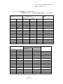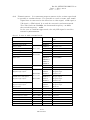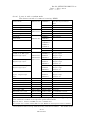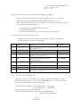
1
M T P C I− D D 2 Monochrome sequential image capture board (画像入出力基板) Operation Manual (取扱説明書) MICROTECHNICA Co., Ltd. (株)マイクロテクニカ 1/116 Microtechnica Doc.No: MTPCI-DD OM-E V1.01 Date: 1 May, 2003 Rev.: 1.01 Declaration The products MTPCI-D D 2 Monochrome sequential image capture board to which this declaration relates are in conformity with the following standards or other normative documents: EN 55022: 1998 + A1: 2000 Class A Information technology equipment - Radio disturbance characteristics - Limits and methods of measurement EN 55024: 1998 + A1: 2000 Information technology equipment - Immunity characteristics - Limits and methods of measurement following the provisions of EMC directive 89/336/EEC as amended by 92/31/EEC and 93/68/EEC. Subject products are manufactured and tested according to appropriate quality control procedures. Warning This product is able to use simultaneous 4 boards. In usage of the condition, this product is matching EMC and also FCC standard. In the case that you use the BNC connector , you wind to 1 time the BNC cable to a ferrite core and please use. Wear wristband etc. in the case that you contact this product when the product is acting and please pay attention so that static electricity is not transmitted to this product. The external triggerd-signals is not connected to the standard camera cable. Please use the exclusive use cable in the case that you want to use the external triggerd-signals irrespective of the above standard. Cable is wound to 1 time to the ferrite core. EMC、FCC 規格への適合宣言 製品、MTPCI-DD(モノクロ2入力画像入出力基板)が下記の規格に適合していること を当社自身の責任において宣言します。 指令:EN55022:1998+A1:2000 Class A 設備の技術的内容−−最大放射特性値および測定方法 指令:EN55024:1998+A1:2000 設備の技術的内容−−最大イミュニティ特性値および測定方法 これらの指令は 89/336/EEC で決められ、92/31/EEC および 93/68/EEC で改訂された EMC の指令に従っています。本製品は品質管理された工程により製造および検査されています。 本基板は4枚を同時使用できます。その状態でEMC及びFCC規格を取得していま す。BNC コネクタを使用する場合は付属の2個のフェライトを BNC ケーブルに1巻 して使用してください。また動作中、本基板に接触する場合はリストバンドなどを着 用し、静電気が本基板に伝わらないように注意して下さい。標準のカメラ用ケーブル には外部トリガ出力は接続されていません。上記の規格に関係なく外部トリガを使用 したい場合は専用のケーブルを使用して下さい。 2/116 Microtechnica Doc.No: MTPCI-DD OM-E V1.01 Date: 1 May, 2003 Rev.: 1.01 Copyright Notice 2003 Microtechnica Co., Ltd. All rights reserved. Without the written permission of Microtechnica, Microtechnica prohibits to copy any portion of this manual. It sometimes changes without notice the specifications of this product and also the contents of this manual. Microtechnica assumes no responsibility to the influence that happens by the use of this product. Company name, product name that are described to this manual are trade mark, or, trademark of each company. 本書のいかなる部分も弊社に無断で複写、転載、複製、改変するを禁止します。 本製品、及び本書の内容については予告なく変更することがあります。 本製品を使用した場合の他への影響の責任は一切負いかねます。 本書に記載されている会社名、製品名は各社の登録商標、または、商標です。 Attention on use: Please use it in the appropriate environment where this product was designated with this manual. As for the use in other environment, there is the fear of a wrong action. Solder face etc. of this product the hand please do not touch directly. There are the fear of an injury and malfunction. In the case that you incorporate this product to a personal computer or this product be connected to a camera please do after you turn off the power supply. Please use the cable that matches fit the camera, in the case that this product and camera are connected. There is the fear that damages the camera and this product, in the case that the cable with different pin arrangement is used. 使用上の注意: 本製品は本マニュアルで指定された適切な環境でご使用ください。その他の環境での使用は誤動 作の恐れがあります。 本製品のハンダ面などには手を直接に触れないでください。ケガや故障の恐れがあります。 本製品をパソコンに組み込む場合またはカメラに接続するは電源を切ってから行ってください。 本製品とカメラを接続する場合、カメラに合った適合するケーブルを使用してください。ピン配置が あわないケーブルを使用すると、カメラや本製品を破損する恐れがあります。 3/116 Microtechnica Doc.No: MTPCI-DD OM-E V1.01 Date: 1 May, 2003 Rev.: 1.01 About the guarantee: Guarantee period depends on the prescription of our company. The guarantee period of the gratuitous repair is 1 year in principle.The carriage is a user burden. Even if it is a gratuitous period the repair in location becomes onerous. It becomes an onerous repair in the case of the malfunction that originates from the responsibility of the user, even if it is a gratuitous period. In the case that the user did reconstruction, repair to this product it becomes onerous. In the case of the repair, the gratuitous repair is in the case of the malfunction of the same part. In this case the half year is a gratuitous period. Even if it is guarantee period inside in the case that there is not user registration it becomes an onerous repair. 保証について: 保証期間は弊社の規定によります。無償修理の保証期間は原則として1年間です。 送料はユーザ負担です。無償期間であっても現地での修理は有償となります。 無償期間であっても、ユーザの責任に起因する故障の場合は有償修理となります。 本製品に対してユーザにおける改造、修理がある場合は有償となります。 その場合により修理できないこともあります。 再修理の場合、無償修理は同一部品の故障の場合です。この場合は半年が無償期間です。 ユーザ登録が無い場合は保証期間内であっても有償修理となります。 4/116 Microtechnica Doc.No: MTPCI-DD OM-E V1.01 Date: 1 May, 2003 Rev.: 1.01 (1) Confirmation of the delivery commodity (納品物品の確認) Accessories of this product confirm whether they are all together. (本製品の付属品がそろっているかを確認ください。) ・ Board main body(基板本体) MTPCI-DD 1 sheet ・ CD-ROM of the belonging(付属の CD-ROM) 1 sheet Contents of CD-ROM(CD-ROM の内容) : 1) Driver program for os(win 2000, win 95, win NT)(OS対応ドライバー) 2) Library program of the DMA board and VC, VB Sample program (Sauce listing and EXE. form),Camera set program. (DMA 基板用ライブラリ、VC とVB のサンプルプログラム(ソースと実行形式)、 カメラ設定プログラム) 3) D o c u m e n t OperationManual(取扱説明書)(English edition, Japanese version) File of the explanation book regarding camera setting (カメラ設定ファイル解説書)(Only the Japanese version) Library specifications(ライブラリ仕様書)(Only the Japanese version) VB sample program manual(VB サンプルプログラム説明書)(Only the Japanese version) VC sample program manual(VC サンプルプログラム説明書)(Only the Japanese version) (2) Introduction of camera cable (the different sale)(カメラケーブルの紹介:別売り) The cameras of various makers are able to connect to this product. The pin number of the connector that an input-output signal is connected may differ by the camera. There is the fear that damages it if it does not connect the camera and this product correctly.The cable of the exclusive use in accordance with the camera is being prepared with different sale in our company. Please use it. いろいろなメーカのカメラが本製品に接続できます。カメラにより入出力信号が接続されて いるコネクタのピン番号が異なる場合があります。カメラと本製品を正しく接続しないと破損 する恐れがあります。弊社ではカメラに合わせた専用のケー ブルを別売りで用意しています。 ご利用下さい。 Camera cable-A (the our company style No.: DMC-BC-A) Correspondence camera: SONY XC-55, NEC TI-400, 480, 1200, 1250 etc. Camera cable-B (the our company style No.: DMC-BC-B ) Correspondence camera: SONY XC-ST, 30,50,70, NEC TI-400, 480, 1200, 1250 etc. Camera cable-C (the our company style No.: DMC-BC-C) Correspondence camera: SONY XC-75, 7500 etc. 5/116 Microtechnica Doc.No: MTPCI-DD OM-E V1.01 Date: 1 May, 2003 Rev.: 1.01 Camera cable-D (the our company style No.: DMC-BC-D) Correspondence camera: SONY XC-HR300 TELI CS3720 etc. (3) About user registration(ユーザ登録について) You are able to register it with the homepage of our company.Or please fax the contents of the following model to the sales department address. (弊社のホームページにて登録できます。または下記の様式の内容を営業部宛にFAXし てください。) User registration form(ユーザ登録用紙) MICROTECHNICA Co. , Ltd. (株)マイクロテクニカ Maintenance department of Sales department 営業部 FAX:03−3986−2549 HP:http://www.microtechnica.co.jp Product name Serial number 製品名 シリアル番号 Company name 会社名 Executive 役職 Name 氏名 Address 住所 Telephone 電話 E-mail: Assignment 所属 フリガナ Facsimile FAX Opinion ご意見 6/116 Microtechnica Doc.No: MTPCI-DD OM-E V1.01 Date: 1 May, 2003 Rev.: 1.01 (4) About the inquiry of the technology contents (技術内容の問い合わせについて) This product regarding technical furthermore you request an inquiry with E-mail or fax. Please fax it to the sales department address with the following model. (本製品に関する技術的なお問い合わせはE−ma i l またはFAXでお願いします。 下記の様式で営業部宛にFAXしてください。) Question of the technology contents(技術内容の質問) MICROTECHNICA Co., Ltd. (株)マイクロテクニカ Service department of Sales department 営業部 FAX:03−3986−2549 HP:http://www.microtechnica.co.jp Company name 会社名 Executive 役職 Name 氏名 Address 住所 Telephone 電話 E-mail: Assignment 所属 フリガナ Facsimile FAX The question(質問) 1. 2. The reply(回答) 1. 2. 7/116 Microtechnica Doc.No: MTPCI-DD OM-E V1.01 Date: 1 May, 2003 Rev.: 1.01 (5) About the repair request(修理依頼について) In the case that you ask the repair of this product you enter the malfunction contents, symptoms in the following model and please send to repair department with the product. It breaks out well that the malfunction contents do not reproduce by use environment. Please let me know the point in the case that you are able to borrow use environment. (本製品の修理を依頼する場合、故障内容、症状 を下記の様式に記入して製品と一緒に保守課へお送りください。使用環境により故障内容 が再現しないことがよく起こります。使用環境をお借りできる場合はその旨をお知らせくださ い。) 8/116 Microtechnica Doc.No: MTPCI-DD OM-E V1.01 Date: 1 May, 2003 Rev.: 1.01 Repair request(修理依頼) MICROTECHNICA Co., Ltd. (株)マイクロテクニカ Maintenance department of Turugashimajigyousho 鶴ヶ島事業所 保守課 TEL: 049−287−6888 FAX: 049−287−6877 HP:http://www.microtechnica.co.jp Destination: Turugashimajigyousho 5-12-1 Suneori-chou ,Turugashima-shi, Saitama-ken 350-2211, Japan MICROTECHNICA Co., Ltd. Maintenance department of Turugashimajigyousho 送り先:〒番号350−2211 埼玉県鶴ヶ島市脚折町5−12−1 (株)マイクロテクニカ 鶴ヶ島事業所 保守課 HP: http://www.microtechnica.co.jp Product name Serial number 製品名 シリアル番号 Address, Return address of the repair article, Payment method ご連絡先、修理品の返送先、修理代金の支払い方法 Company name 会社名 Executive 役職 Name 氏名 Address 住所 Telephone 電話 E-mail: Assignment 所属 フリガナ Facsimile FAX Payment method 支払い方法 Purchase store 購入先 Reign favor(代引き)―― Bank payment(銀行振込)―― Company name: Name: Telephone: Fax: Malfunction contents/symptoms(故障内容・症状) Use environment 使用環境 Repair contents 修理内容 9/116 Microtechnica Doc.No: MTPCI-DD OM-E V1.01 Date: 1 May, 2003 Rev.: 1.01 Contents 1.Outline ・・・・ 6(E) 2.Characteristic ・・・・ 7(E) 3.Constitution of the Board 3.1 Connection with the camera ・・・・ 8(E) 3.2 Connection with the monitor ・・・・ 10(E) 4.Specification of hardware 4.1 Input video signal ・・・・ 11(E) 4.2 Output video signal ・・・・ 12(E) 4.3 Sampling frequency of the image data ・・・・ 12(E) 4.4 Frame memory ・・・・ 13(E) 4.5 I/O-access ・・・・ 14(E) 4.6 Power supply and Dimension ・・・・ 14(E) 4.7 Environment Condition of Use ・・・・ 14(E) 5.PCI-bus ・・・・ 15(E) 6.Interface with a program 6.1 I/O port ・・・・ 17(E) 6.2 Command registration ・・・・ 18(E) 6.3 Status registration ・・・・ 19(E) 6 . 4 Mode registration ・・・・ 20(E) 6.4.1 Setting of the camera ・・・・ 20(E) 6.4. 2 Setting of the shutter control ・・・・ 21(E) 6.4.3 Setting of the clock-1 ・・・・ 22(E) 6.4.4 Setting of the clock-2 ・・・・ 23(E) 6.4.5 Setting of the IO signal ・・・・ 24(E) 6.4.6 Setting of the monitor ・・・・ 24(E) 6.5 Setting of the counter for the camera signal ・・・・ 25(E) 6 . 6 Setting of the counter for the monitor display ・・・・ 26(E) 6 . 7 Selection of wide use IO and camera signal ・・・・ 27(E) 6.8 External trigger ・・・・ 31(E) 6 . 9 DMA forwarding to the system memory ・・・・ 31(E) 6 . 1 0 Forwarding from the system memory to buffer memory for the monitor ・・・・ 33(E) 10/116 Microtechnica Doc.No: MTPCI-DD OM-E V1.01 Date: 1 May, 2003 Rev.: 1.01 Data volume A. List of the command B. Example of setting B.1 Example of the setting to a camera (1) Video signal of the EIA standard (2) Camera of SONY (3) Camera of NEC (4) Camera of JAI (5) Camera of TELI (6) Camera of the Takenaka system B . 2 Example of the setting to a monitor (1) VGA monitor (2) Setting of superimpose B . 3 Example of the setting to DMA forwarding (1) Image catch by DMA forwarding (2) Forwarding to the buffer memory for the monitor by DMA forwarding 11/116 Microtechnica 1. Outline This Operation Manual is describing the hardware explanation with regard to MTPCI-DD. You incorporate this board to a personal computer of PCI bus installation and use it. This board inputs the video signal from a camera and digitizes. And it forwards the data to the system memory in the personal computer by DMA forwarding. Also, the contents of the output buffer memory that are installed to this board can be displayed to a VGA monitor. 4 boards of this product are able to be installed to 1 personal computer simultaneously. It is possible control this board easily when the driver routine of the boards is used. A fundamental library is available to process the image data that was taken to the memory. Please pay attention so that the forwarding mistake does not result in consideration of the restriction of the forwarding speed of a PCI bus, in the case that 4 boards are used simultaneously. System configuration example MTPCI−DD Monochrome CCD camera VGA Monochrome standard monitor CCD camera PCIbus DMA forwarding Personal computer of marketing 1/116 Microtechnica Doc.No: MTPCI-DD OM-E V1.01 Date: 1 May, 2003 Rev.: 1.01 2. Characteristic This board is able to connect 2 cameras with 1 board. Also, this board is able to input the video signals of the various cameras, such as a camera of 2 times speed and a camera of 2 line output types. When you use ‘The camera setting program’ and the various library programs, you are able to set up the various conditions to the camera easily. Image data can be taken easily to a system memory. ① ② ③ ④ ⑤ ⑥ ⑦ ⑧ ⑨ ⑩ ⑪ ⑫ The various cameras of the analogue signal for industry are possible connect. Two cameras are possible connect with, and be possible a simultaneity catch. The cameras of 2 line output type or the progress type or the interlace type is possible connect. The video sampling clock is able to select from 5MHz until 40MHz. This board is able to correspond to internal synchronous camera and external synchronous camera. This board is able to forward image data to a system memory by DMA forwarding. This board is preventing the forwarding leakage of image data, because it is installing it with the buffer memory of the 512K bytes. This board can transform the signal of 1 horizontal line until 4096 dots. This board is able to input the signals until 4096 lines. This board can control a random shutter function of a camera. This board is installing the frame memory(the output buffer memory) of the 1M bytes for a monitor display. Data of a frame memory can be output with the video signal of a VGA quasi-standard. 2/116 Microtechnica Doc.No: MTPCI-DD OM-E V1.01 Date: 1 May, 2003 Rev.: 1.01 3 . Constitution of the Board 3.1 Connection with the camera As for the method of the connection with the camera, there are the following 2 method. One case is the connection by a DSUB-15P pin connector. With this connection for a camera an external synchronous control becomes possible. Another case is the connection by a BNC connector. With this connection, this board uses the synchronization of the NTSC composite video signal. ① ② Camera connection DSUB- Wide use Di/o 15P BNC connector Video input1 BNC connector Video input 2 DSUBVGA output MTPCI-DD 15P PCI bus Video input-1:BNC-A Signal AGND VINA Common for the camera Input of the video signal. –CH−A Video input-2:BNC-B Signal AGND VINB Common for the camera Input of the video signal. –CH−B 3/116 Microtechnica Doc.No: MTPCI-DD OM-E V1.01 Date: 1 May, 2003 Rev.: 1.01 Table 3.1 The assignment of the pin number of the connector for the camera (DSUB-15P)-Signal name for the camera and signal name of a wide use Pin No. Camera signal name Usage Wide use DI/DO signal name 1 AGND Common for the camera 2 +12V The DC 12V power supply for the camera. 3 AGND Common for the camera 4 VIN-A Input of the video signal. ---CH-A ( i n p u t ) 5 HD-A Horizontal synchronous signal---CH-A(in/out) OUTB0, INB0 (Input-output signal of TTL) 6 V D-A Vertical synchronous signal ---CH-A(in/out) OUTB1, INB1 (Input-output signal of TTL) 7 GTRG-B The external triggered OUTB6, NB6 signal---CH-B (input) Input-output signal of TTL) 8 GTRG-A The external triggered signal---CH-A(input) OUTB7, INB7 (Input-output signal of TTL) 9 AGND Common for the camera 10 VIN-B Input of the video signal. ---CH-B (input) 11 HD-B Horizontal synchronous signal---CH-B(in/out) OUTB4, INB4 (Input-output signal of TTL) 12 V D-B Vertical synchronous signal ---CH-B(in/out) OUTB5, INB5 13 STRG-A Shutter trigger signal ---CH-A(output) OUTB2, INB2 (Input-output signal of TTL) 14 STRG-B Shutter trigger signal ---CH-B(output) OUTB3, INB3 15 GND Common for the digital signals *1 *2 *2 (Input-output signal of TTL) (Input-output signal of TTL) *1: The d.c 12V power supply for the camera is using the d.c 12V power supply of a personal computer. Please pay attention to the consumption current. It does not connect the load of 0.5A over. * 2 : A video signal(VIN) is connected to the BNC touching plug and also DSUB-1 5 P inside the board. A video signal is terminated with a 75Ω. 4/116 Microtechnica Doc.No: MTPCI-DD OM-E V1.01 Date: 1 May, 2003 Rev.: 1.01 3.2 Connection with the monitor This board is able to display the data of the buffer memory in the multiple scan monitor for a general personal computer. Table 3.2 The assignment of the pin number of the connector for the VGA monitor (DSUB-15P) Pin No. 1 Signal ROUT Usage R−Video output 2 G OUT G−Video output The maximum value of video signal level is 0.7V. It is terminated with a 75Ω. 3 B OUT B−Video output The maximum value of video signal level is 0.7V. It is terminated with a 75Ω. 4 R IN R−Video input The maximum value of video signal level is 0.7V. It is terminated with a 5Ω. (in the case of superimposition ) 5 G IN G−Video input The maximum value of video signal level is 0.7V. It is terminated with a 75Ω. The maximum value of video signal level is 0.7V. It is terminated with a 75Ω. (in the case of superimposition ) 6 B IN B−Video input The maximum value of video signal level is 0.7V. It is terminated with a 75Ω. (in the case of superimposition ) 7 GND GND Common 8 GND GND Common 10 GND GND 11 HD IN 9 Common Horizontal synchronous TTL (in the case of superimposition) (in the case of superimposition) signal input 12 VD IN Vertical synchronous signal input TTL 13 HD OUT Horizontal synchronous TTL 14 VD OUT signal output Vertical synchronous TTL signal output 15 *: The output signal of the above table is the signal for VGA output. *: There is VGA output of only this board, also there is the superimposition VGA output of this personal computer output and of the board output. *: In the case of superimposition mode, the input signal of the above table connects personal computer VGA output. *: This board is able to input and output a monochrome picture only. As for the output from this board the RGB same image data is output. 5/116 Microtechnica Doc.No: MTPCI-DD OM-E V1.01 Date: 1 May, 2003 Rev.: 1.01 4. Specification of hardware 4.1 Input video signal This board is able to input 2 channels of the monochrome video signal. Items Explanation Number of Two input channels Two cameras of 1 line output are able to Input be connected or one camera of 2 line output is able to be connected. Input signal The monochrome 1Vpp 75Ω terminatted、(Video – positive, Composite video signal Synchronous - negative ) or 0.7Vpp - Only a video signal Horizontal synchronous frequency Setting with the program Range:1KHz∼60KHz Vertical synchronous Setting with the program frequency Range:1Hz∼100Hz Scanning Non-Interlace method 2:1-interlace or Setting with the program BNC connector、 Kind of the connector DSUB-15P connector External HD output signal, synchronous VD output signal Internal HD input signal, synchronous VD input signal, Setting with the program Setting with the program Composite video signal Trigger control Setting with the program 6/116 Microtechnica Doc.No: MTPCI-DD OM-E V1.01 Date: 1 May, 2003 Rev.: 1.01 4.2 Output video signal It is the output video signal for a monitor. a monitor of multi-scan correspondence. It is able to connect to Items Explanation Output signal R, G, B video signal 0.7Vpp 75Ω terminated. Horizontal Setting with the program synchronous frequency Vertical synchronous Setting with the program frequency Scanning Non-Interlace method Kind of the DSUB-15P connector. connector Three lines’ connector of a shrink type External HD input signal and synchronous VD input signal 4.3 TTL (in the case of superimposition) Sampling frequency of the image data (1) In the case of external synchronization: The range : 5∼40MHz . The setting step : about 63kHz. (2) In the case of internal synchronization: The video clock: 24.5454MHz, 12.2727MHZ, 8.18MHz, 6.14MHz. (3) A/D converter : 8 bits, high speed flash types. Transformation frequency : 40MHz(MAX) in monochrome use. 7/116 Microtechnica Doc.No: MTPCI-DD OM-E V1.01 Date: 1 May, 2003 Rev.: 1.01 4.4 Frame memory This board is installing the FIFO buffer memory of the 1M byte for the image data output. Also, the FIFO buffer memory of the 512K bytes for the DMA forwarding is being installed. Fig. 4.1 The flow of image data Input signals for camera ADC FIFO PCI9080 CPLD ADC FIFO PCI bus Control of synchronous FIFO-V and camera control FIFO-V DAC VGA Monitor Generation of theClock and Synthesis setting to a minute frequency Board 8/116 Microtechnica Doc.No: MTPCI-DD OM-E V1.01 Date: 1 May, 2003 Rev.: 1.01 4.5 I/O-access This board is using the io-address of 6 ports. Those ports is necessary to catching the image data and to setting of parameter etc.. Address of the port is allocated in the unit of 4 bytes. Port Address I/O Access Object No. Port 0 xx00H OUT byte Command-register Port 0 xx00H IN byte Status-register Port 4 xx04H IN/OUT byte Input-output bit of wide use IO Port 8 xx08H OUT byte/word Setting of the mode register Port 8 xx08H IN longword The line counter for DMA forwarding---A −A −A SR:0 Port 8 xx08H IN word Progress counter from GTRG input---A SR:24H Port 8 xx08H IN word Progress counter from GTRG input ---B SR:25H Port c xx0CH OUT byte Select the SR-register Port c xx0CH IN longword The line counter for DMA forwarding ---B Port 10 xx10H OUT byte Command-register ---B Port 10 xx10H IN byte Status-register --- B Port 14 xx14H OUT byte Pointer clear of the output buffer memory for a monitor. 4.6 Power supply and Dimension Rated Voltage (V) +5V±5% +12V±10% -12V±10% 4.7 Rated Current (A) 0.5A 0.8A 0.05A Outer Dimension L×W×H 175×106×16 Environment condition of Use Bus specification Ambient Temperature Ambient Humidity Dust Corrosiveness gas : PCI quasi-standard. :0∼50℃ :80%RH with no dew condensation : Especially to be not many : A nonexistent case 9/116 Microtechnica Doc.No: MTPCI-DD OM-E V1.01 Date: 1 May, 2003 Rev.: 1.01 5. PCI bus This board is installing the PCI bus chip (PCI 9080) made in PLX. Only the DMA channel 0,1 function is being used. Setting of the internal register of the PCI bus chip becomes needed, in the case that the DMA channel is used. Table 5.1 Contents of the PCI configuration Address 00H I/o I/O Access word 04H 08H 0CH 10H I/O I/O I/O I/O word word word word 14H 18H I/O I/O word word Object DeviceID/VenderID Value in this board ―[4444 4D54] Status/Command ClassCode/Revision ID BIST/H Type/PCI Latency/C L Size PCIBAR0 PCI base address Internal register of memory map PCIBAR1 PCI base address Internal register of i/o map PCIBAR2 PCI base address I/O ports 1CH 20H 24H 28H 2CH I/O word Subsystem-DeviceID/VenderID [4444 4D54] 30H 34H 38H 3CH I/O word Max_Lat/Min_Gnt/Int Pin/Int Line *1: 4D54(MT): PCI-VenderID of MicroTechnica. 4444(DD): PCI-DeviceID of this board. *2: This address is the base address to access a internal register of the PCI-9080. In the case of memory mapping access, PCIBAR0 is used. In the case of i/o mapping access, PCIBAR1 is used. In the case of i/o ports of this board, PCIBAR2 is used. **: The least significant bit of the base address is making 0. 10/116 Microtechnica *1 *2 *2 *3 *1 Doc.No: MTPCI-DD OM-E V1.01 Date: 1 May, 2003 Rev.: 1.01 In the case that a DMA channel is used, setting of the PCI 9080 internal register is necessary. The following only register is set up and do not set up the other register. Address 80H 84H 88H 8CH 90H 94H 98H 9CH A0H A4H A8H I/o OUT OUT OUT OUT OUT OUT OUT OUT OUT OUT I/O Access Longword Longword Longword Longword Longword Longword Longword Longword Longword Longword Longword Object DMA Ch DMA Ch DMA Ch DMA Ch DMA Ch DMA Ch DMA Ch DMA Ch DMA Ch DMA Ch DMA Ch 11/116 Microtechnica 0 Mode 0 PCI Address 0 Local Address 0 Transfer Byte Count 0 Descriptor Pointer 1 Mode 1 PCI Address 1 Local Address 1 Transfer Byte Count 1 Descriptor Pointer Command/Status Register Doc.No: MTPCI-DD OM-E V1.01 Date: 1 May, 2003 Rev.: 1.01 6. 6.1 Interface with a program Input/output port This board is using the io-address of 6 ports. The base address sets up it with "PCIBAR2". It is allocated in i/o space of 16 bits and monopolize 32 bytes. Port No. Address I/O Access Object Port 0 xx00H OUT Byte Command-register --- A Port 0 xx00H IN Byte Status-register Port 4 xx04H IN/OUT Byte Input-output bit of wide use IO Port 8 xx08H OUT Byte/Word Setting of the mode register Port 8 xx08H IN Longword The line counter for DMA forwarding ---A SR:0 Port 8 xx08H IN Word Progress counter from GTRG input --- A --- A SR:24H Port 8 xx08H IN Word Progress counter from GTRG input --- B SR:25H Port c xx0CH OUT Byte Select the SR-register Port c xx0CH IN Longword The line counter for DMA forwarding---B Port 10 xx10H OUT Byte Command-register --- B Port 10 xx10H IN Byte Status-register Port 14 xx14H OUT Byte Pointer clear of the output buffer memory --- B for a monitor. *1: A byte port it is able to access with the word. In the case that it uses it as output the upper byte is disregarded. In the case that it uses it as input the upper byte becomes uncertain. 12/116 Microtechnica Doc.No: MTPCI-DD OM-E V1.01 Date: 1 May, 2003 Rev.: 1.01 6.2 Command register The command register sets up it with port 0, port 10. The command control the catching method of image data. Only the byte access is. Port 10 becomes for camera B and port 0 for camera A. It do even the take-in of camera B only with a command of port 0, in the case that the CMDMD bit is 1. Port D7 D6 D5 D4 0H Camera-A GETC GMOD DDMD - 10H Camera-B GETC GMOD DDMD - GETC =1 Image catch instructions. GMOD =0 =1 Setting ofa catch mode. =0 DDMD Setting of the forwarding mode. (Setting of the processing of remainder data) GETMC Image catch instructions to the output buffer memory GMMD Setting of catch mode to the output buffer memory GMSL Image selection command =1 =0 =1 =0 =1 D3 GETMC - D2 GMMD - D1 GMSL - D0 - The image catch from a video signal is started. This bit becomes 1 with the next vertical synchronous signal. DMA forwarding is finished automatically when the byte number that was set up is input. Input of the image is finished. Plural screen of the image data is taken. DMA forwarding byte number corresponding to the screen number that takes it is set up. Take-in data number relys on the byte that forwards it by DMA. A forwarding byte number is set up with the data number of the screen unit. In the case that the data number does not agree the input data is not guaranteed. Image data of 1 screen is taken. And the data number of 1 screen must agree with the byte number of DMA forwarding. Remainder data is forwarded forcibly in the unit of each screen. The input data is not guaranteed when the next screen input begins before this DMA forwarding ends however. Please use this mode, only when there is a sufficient margin in the share of the PCI bus. Compulsory DMA forwarding time ends with about 100µ S . In the case of GMOD=0 and 1 screen input, the DMA forwarding is carried out irrespective of a DDMD bit. Remainder data does to as it is. This remainder data is forwarded by the DMA with the next screen input. Only the remainder data of the final screen causes to forward it forcibly by the DMA. Data of the camera is taken to the output buffer memory for a monitor and the contents change by top writing. The actual catch is carried out from the next vertical synchronous signal. Data does not be taken to the output buffer memory. =0 It continuously catch the image data. Until this bit is set up in 0, it is catching the deta and forwarding to the output buffer memory. In the case of a continuation catch, data is done top writing because the memory capacity is 1 frame. It is the catch-mode of only 1 screen. =1 =0 Data of camera-B is taken to the output buffer. Data of camera-A is taken to the output buffer. 13/116 Microtechnica Doc.No: MTPCI-DD OM-E V1.01 Date: 1 May, 2003 Rev.: 1.01 6.3 Status register You input the status register with port 0, port 10. It is the register that monitors the condition where takes an image. Only the byte access is. Port 10 becomes for camera B and port 0 for camera A. Port D7 D6 D5 D4 D3 D2 D1 D0 0H Camera-A GETG GETS GETMG NSVD FLDG DMAG DMAER - 10H Camera-B GETG GETS GETMG NSVD FLDG DMAG DMAER - GETG GETS =1 =0 =1/0 GETMG =1 NSVD =0 =1 FLDG =0 =1 =0 DMAG =1/0 DMAER =1/0 It becomes 1 with the output of the GETC-command It becomes 0 with the completion of image catch. It becomes 1 after the next vertical synchronous signal, after the GETC-command was output. It becomes 0 with the completion of image catch. It is 1 while the image data inputs it to the output buffer memory for a monitor. It becomes 1 with the output of the GETMC-command. It becomes 0 with the completion of image catch. It becomes 1 at the time of period throughout of a vertical synchronous signal. It becomes 0 other than the period of a vertical synchronous signal. It is effective with an intelace mode. In the case that the screen that took it first is an ODD field it becomes 1. I In the case that the screen that took it first is an EVEN field it becomes 0. It is 1 during DMA forwarding. After forwarding ends it is delayed 50 ∼100μS and become 0. In the case that the forwarding mistake resulted it becomes 1. It is held until the next GETC-command is output in the case that it became 1. *: The data forwarding ability of the PCI buses of 32 bits, 33MHz are biggest 133MHz/S. The actual speed is below this forwarding speed. 14/116 Microtechnica Doc.No: MTPCI-DD OM-E V1.01 Date: 1 May, 2003 Rev.: 1.01 6.4 Mode register The SR cord (the SR register) of port 8 is set up in port C. A SR cord is set up with 6 bits of D0∼D5. Port C is byte access. The mode and counter are set up with port 8. The access is only the output. As for the access of port 8 the byte and word are possible. The upper byte is disregarded, in the case that it gained access to the setting of the byte register with the word. The list of the command is shown below (the SR cord: 0 to 8). Port SR D7 CH - D6 D5 SR6 D4 SR5 SR4 D3 D2 SR3 8H SR=00 8H SR=01 RNDST 8H SR=02 ITRSM ITRGM 8H SR=03 EHCKS1 EHCKS0 8H SR=05 BIOMD7 BIOMD6 BIOMD5 BIOMD4 BIOMD3 8H SR=06 SPOL7 SPOL6 SPOL5 SPOL4 8H SR=07 SMOD7 SMOD6 SMOD5 SMOD4 8H SR=08 OVMD 6.4.1 Condition setting of a camera. CMRMD CMDMD SYCMD1 SYCMD0 MQCKS CLKSEL SR1 D0 SR0 CMRMD STRMD2 STRMD1 STRMD0 CLKDV0 CCKDV1 CCKDV0 STCKS1 STCKS0 BIOMD2 BIOMD1 BIOMD0 SPOL3 SPOL2 SPOL1 SPOL0 SMOD3 SMOD2 SMOD1 SMOD0 CLKDV1 OITRSM Setting of the camera SR=00 GTSMD SR2 D1 HVPOL ----SR=0 0:One line output camera 1:Two line output cameras 0:The camera of 1 line output is able to be connected to 2 units. As for 2 cameras, there is the same necessity. 1:One camera of 2 line output is able to be connected CMDMD GTSMD 0:Camera-A or camera-B 1:A+B 1:GETC to camera-A, B are output with GETC of port 0. When CMDMD is set up in 1, the GETC-command of port 0 is output to both A, B, in the case that a camera is 2 line output camera. 0:It is in the case that you want only one side of a camera as GETC. The GETC-command is output separately A, B. 0:6,7 (7:Camera-A or 6:camera-B ) 1:7(both camera) 0: The image data is taken each time the INB 6,7 signal is input, if the GETC-command is output, in the case that INB6, INB7 is used as the GTRG signal. 1: It becomes the catch signal of A, B camera with only the signal of INB7. 15/116 Microtechnica Doc.No: MTPCI-DD OM-E V1.01 Date: 1 May, 2003 Rev.: 1.01 6.4.2 Setting of the shutter control SR=01 Mode setting of a camera ----SR=1 RNDST 0:Normal scan, triggering every VD of a shutter sequence. 1:Random scan. At the time of image catch you trigger it with a program. SYCMD1, 0 0:external-HV 1:external-H 2:internal-C 3:internal-HV (Synchronous 0:A camera is synchronized by using HD/VD synchronous signal of mode) the board. 1:A camera is synchronized by using the HD signal of the board. A VD signal extracts from the video signal of the camera and use it. 2:A board is operated with the video signal of a camera. HD/VD signal is extracted from the video signal of the camera and use it. 3:A board is operated with HD/VD signal of a camera. The INB 0,1 signal of the connector is used as HD/VD signal. STRMD2, 1, 0 0:NRM 1:TRG 2:TRG-VD 3:VD-TRG 4:TRG-TRG 0:It is the mode that does not do a shutter control. Even in the case that the shutter control is carried out on the side of the camera it is this mode. 1:A shutter is controlled with only the STRG signal. It uses it for the camera that shutter time is decided with the pulse width of the STRG signal. Or it uses it for the camera that a STRG signal is used as the trigger signal only. STRG signal of the pulse width that the TRGW-counter set up is produced. The STRG signal ends and after 3 or 4HD the VD signal is produced and the image catch is started. 2:A shutter is controlled between the STRG signal and VDsignal. It uses it for the camera that shutter time is decided between the STRG signal and VD signal. STRG signal is occurred and VD signal is produce after the pulse width that the TRGW counter set up. STRG signal width becomes 1 clock of a TRGW counter clock. 3:Shutter is controlled between a VD signal and STRG signal. It uses it for the camera that shutter time is decided between the VD signal and STRG signal. VD signal is occurred and the STRG signal is produce after the pulse width that the TRGW counter set up. STRG signal width becomes 1 clock of a TRGW counter clock. 4:A shutter is controlled between 2 STRG signals. It uses it for the camera that shutter time is decided between 2 STRG signals. STRG signal is occurred and the 2nd STRG signal is produce after the pulse width that the TRGW counter set up. STRG signal width becomes 1 clock of a TRGW counter clock. The 2nd STRG signal ends and after 3 or 4HD the VD signal is produced and the image catch is started. 16/116 Microtechnica Doc.No: MTPCI-DD OM-E V1.01 Date: 1 May, 2003 Rev.: 1.01 6.4.3 Setting of the clock-1 SR=02 ITRSM Setting of a clock ITRGM MQCKS (Resource clock) ----SR=2 0: Non-interlace 1: 2:1 -interlace When it is non-interlace mode it becomes image catch of a field unit. The catch of the image data is started from the next VD signal in the non-interlace mode. 0:The 1st field 1:Field immediately after triggering 1:The catch of the image data is started from the next VD signal in the case of the interlace camera. However, it becomes uncertain from which field it started the catch. In the case of the interlace camera the data that was forwarded DMA is divided in the front the second half of the memory. Determination of the field is possible with theFLDG-status bit. If FLDG bit is 1, data of the 1st field is sent in the memory first half, and the data of the 2nd field is sent in the memory second half. If FLDG-bit is 0 it is reverse. 0:The catch of the image data is started from the 1st field in the interlace mode. The catch of the image data is waited maximally 33mS in a usual camera. Data of the 1st field (EVEN) is sent in the memory first half, and the data of the 2nd field(ODD) is sent in the memory second half. 0: 49.0909MH z 1:VCO (62.937KHz×VCA) The resource clock of the board is 49.0909MHz. The input clock is generated from this resource clock. The input clock is able to be set up in the range of 5M∼40MHz in the case of an external synchronous mode. Also, the PLL+VCO circuit for input clock generation is available. The clock frequency is able to be transformed with the setting of the VCA counter. In the case that necessary frequency is not the minute circumference of 49MHz VCO is selected. CLKSEL (Input clock) CLKDV1, 0 It sets up it with MQCKS=0, CLKSEL=1, in the case that the input clock is same the frequency that is done the minute circumference from 49MHz. 24.545MHz half of 49MHz are selected. Clock that was selected becomes the minute circumference of a resource clock and stability becomes best. 0:VCO 1:Half of Resource clock In the case that the frequency is not the minute circumference of 49MHz VCO is selected. Setting up it with CLKSEL=0 in the case that a camera is used with external synchronous mode. VCO is selected. In the case that a camera is not able to use with external synchronous mode, setting up it in MQCKS=1, CLKSEL=1 and 1/2 of VCO are selected. 0:1/1 1:1/2 2:1/3 3:1/4 It does the input clock a minute circumference furthermore. CCKDV1, 0 (camera clock) 0:1/1 1:1/2 2:1/4 3:1/8 Clock for the preparation of the HD signal 17/116 Microtechnica Doc.No: MTPCI-DD OM-E V1.01 Date: 1 May, 2003 Rev.: 1.01 6.4.4 SR=03 Setting of the clock-2 EHCKS1, 0 (Clock for HD/VD detection) STCKS1、0 ----SR=3 0:12M 1:6M 2:3M(NRM) 3:1.5M VD signal and field signal need to be extracted from the video signal of a camera, in the case that a synchronous mode is 1,2. 0:High speed camera etc. Horizontal synchronous frequency is the range of 40∼60KHz (the frequency is a rough standard. ) 1:Two times speed camera etc. Horizontal synchronous frequency is the range of 20∼40KHz(Even the pulse width etc. of a synchronous signal influences. ) 2:Usually camera Horizontal synchronous frequency is the range of 10∼20KHz. 3:Low speed camera etc. Horizontal synchronous frequency is the range of 5∼10KHz. 0:HD 1:VD 2:4μS(252KHz) 3:The clock of shutter control is selected. The clock that uses it for the TRGW counter is selected. It makes the shutter sequence in the circuit of the board and TRG signal, VD signal that were designated are produced automatically and the image data is taken. 18/116 Microtechnica Doc.No: MTPCI-DD OM-E V1.01 Date: 1 May, 2003 Rev.: 1.01 6.4.5 Setting of the IO signal ----SR=5,6,7 The input-output, polarity, usage of the IO signal that use it with port 4 are set up. Port SR D7 D6 D5 D4 D3 D2 D1 D0 8H SR=05 BIOMD7 BIOMD6 BIOMD5 BIOMD4 BIOMD3 BIOMD2 BIOMD1 BIOMD0 8H SR=06 SPOL7 SPOL6 SPOL5 SPOL4 SPOL3 SPOL2 SPOL1 SPOL0 8H SR=07 SMOD7 SMOD6 SMOD5 SMOD4 SMOD3 SMOD2 SMOD1 SMOD0 SR=05 BIOMD7-0 SR=06 SPOL7-0 SR=07 SMOD7-0 6.4.6 Direction of the signal Polarity of the signal Signal mode 0:Input 1:Output 0:Positivelogic 1:Negative logic 0:Wide use I/O 1:Camera use Setting of the monitor ----SR=8 Port SR D7 D6 D5 D4 D3 D2 D1 D0 8H SR=08 OVMD OITRSM HVPOL SR=08 OVMD 0:VGA_S 1:VGA Output 0 : It is a personal computer picture synthesis. It superimposes the Setting mode output image of a personal computer and camera image. of a 1 : It is the display output from a board. Without superimposing it monitor displays the only camera image. OITRSM 0:Non-interlace 1:2:1-interlace In the case that the 2:1-interlace camera is used, if the ITRSM bit is 1 the OITRSM bit is set in 1. 1: The buffer memory is divided in the 512K byte 2 block. The input data of each field is housed in a different memory block. Image output is non-interlace mode. The data output is output alternately each block. 0: It is treated as the 1M byte 1 block. In the case of 2 line output camera the input is non-interlace but it synthesizes 2-line output to put 1 line and it must display it. Therefore the OITRSM bit is set in 1. HVPOL 0:Negative logic 1:Positive logic Polarity of It is the setting of the logic of a synchronous signal. a HD, VD synchronous signal are a negative logic signal generally. synchrono But at the time of SVGA use the ordinariness is used with positive us signal logic. Therefore please set HVPOL in 1 in the case that it uses it with SVGA. If it is a VGA mode the synchronous signal is output with positive logic. If it is a VGA_S mode the synchronous signal that was input is considered as positive logic. Scanning mode 19/116 Microtechnica Doc.No: MTPCI-DD OM-E V1.01 Date: 1 May, 2003 Rev.: 1.01 6.5 Setting of the counter for the camera signal (SR: 10----1 C ) Port CH 8H D12 D11 D10 D9 SR cord SR=10 D8 D7—D0 SR6—SR0 VCA:It sets up it to generate the video clock. 10 bits data (D9∼D0) . Doing the VCO output clock a minute circumference, it makes the comparative signal of the PLL circuit. A PLL circuit controls the VCO circuit so that a standard signal and comparative signal become the same phase. The frequency of VCO output is able to calculate it with the next formula. Clock frequency = 62.937KHz × Setting value of the counter Please set up the value in 160 to 1023 ranges. 8H SR=14 UNBP:The horizontal effective position of an input signal is set up. 9 bits data (D8∼D0). Horizontal clock uses the camera clock. The value of a horizontal effective position is set up with the clock(dot) number from the back edge of the HD signal. 8H SR=15 UNBW:Horizontal effective width of an input signal is set up. 12 bits data. Width is set up with the clock(dot) number from the horizontal effective position. Horizontal width is the setting of 16 clock units. The subordinate position 4 bits are disregarded and become 0. (D11∼D0) 8H SR=16 VUBP:Vertical effective position of an input signal is set up. 8 bits data. (D7∼D0) The vertical counter clock is HD. A vertical effective position sets up the line number from the back edge of the VD signal. 8H SR=17 VUBW:The vertical effective width of an input signal is set up. 12 bits data. (D11∼D0). Width becomes the line number from the vertical effective position of the VD signal. 8H SR=18 HDSC:A horizontal repetition rate is set up. 12 bits data. (D11∼D0). The clock of the counter is a camera clock. In the case that the scanning mode of a camera is the interlace mode the rate is set up to half. In this case output becomes to put 1 piece. 8H SR=19 HDPW:The pulse width in a horizontal synchronous period is set up. 8 bits data. (D7∼D0). Clock of the counter is a camera clock. 8H SR=1A VDSC:A vertical repetition rate is set up. 12 bits data. (D11∼D0). The clock of the counter is an above HD signal. 8H SR=1B VDPW:The pulse width in a vertical synchronous period is set up. 5 bits data. (D4∼D0). The clock of the counter is an above HD signal. 8H SR=1C TRGW:The width of trigger pulse is set up. 10 bits data. (D9∼D0). The circuit of the board produces the TRG signal, VD signal in accordance with appointment automatically and do the catch of image data. The shutter time is set up with the counter. * The resource clock of the board is 49.0909MHz. * The standard signal of the PLL circuit is 62.937KHz. (49.0909MHz/780) 20/116 Microtechnica Doc.No: MTPCI-DD OM-E V1.01 Date: 1 May, 2003 Rev.: 1.01 6.6 Setting of the counter for the monitor display (SR: 30---3 B ) The image data that is housed to the output buffer memory for a monitor is able to display it in the multiple scan monitor for a general personal computer. The output signal is the signal for VGA output. When it superimposes personal computer, the input signal of the board connects the VGA output signal of a personal computer. Because this board is monochrome specification, as for the output of RGB the same image data is output. Port 8H SR=30 8H SR=34 8H SR=35 8H SR=36 8H SR=37 8H SR=38 8H SR=39 8H SR=3A 8H SR=3B D12 D11 D10 D9 D8 D7—D0 OCA:The output video clock for the display is set up. 11 bits data. D10∼D0. The subordinate position 2 bits is disregarded and become 0. A calculation formula is shown below. VGA : Output clock frequency = 62.937KHz × Setting value of the counter VGA_S : Output clock frequency =HD frequency of a personal computer × The setting value of the counter The restriction of the output frequency of the VCO circuit is 10M∼75MHz. At the time of a VGA mode, please set value of the counter with 160∼1190. OUBP:The horizontal effective position of the output signal is set up. 10 bits data. (D9∼D0). The clock of the counter is the output video clock. The position is it which clock number passed from a back edge of a horizontal synchronous signal. It is the setting of 2 clock units. The least significant bit is disregarded and become 0. OUBW:The horizontal effective width of the output signal is set up. 11 bits data. (D10∼D0). The least significant bit is 0. The clock of the counter is the output video clock. Width becomes the pixel number that wants to display it. OVUP:The vertical effective position of the output signal is set up. 9 bits data. (D8∼D0). The clock of the counter is the horizontal synchronous signal (HD). The position is the position which passed only the line number from the back edge of a vertical synchronous signal. OVUW:The vertical effective width of the output signal is set up. 10 bits data. (D9∼D0). The clock of the counter is the horizontal synchronous signal (HD). The width is the line number that wants to display it. OHSC:A horizontal repetition rate of output signal is set up. 11 bits data. (D10 ∼D0). The clock of the counter is the output video clock. The horizontal scan rate is set up as the 16 clocks unit and the subordinate position 4 bits are disregarded and become 0. OHDW:The pulse width in a horizontal synchronous signal is set up. 8 bits data. (D7∼D0). The clock of the counter is the output video clock. The width of the horizontal synchronous signal is set as the 2 clocks unit and the most significant bit is 0 . OVSC:A vertical repetition rate of output signal is set up. 11 bits data. (D10 ∼D0). The clock of the counter is the horizontal synchronous signal (HD). It is set up as the 1 line unit. OVDW:The pulse width in a vertical synchronous signal is set up. 4 bits data. (D3∼D0). The clock of the counter is the horizontal synchronous signal (HD). 21/116 Microtechnica Doc.No: MTPCI-DD OM-E V1.01 Date: 1 May, 2003 Rev.: 1.01 *: The output clock is generated in resource clock 49.0909MHz and PLL+VCO circuit. The memory of the 1M bytes is installed as the output buffer memory for a monitor display. The scan transformation is carried out in the buffer memory block and the VGA output becomes possible. Buffer memory is the memory of a FIFO type and only the sequecial access possible. The length of the XY direction of the monitor is variable length. It is able to use it with the constitution of the free size inside the range of the 1M bytes memory. X-dot Y-li n e Y-Maximum value 640 480 1638 800 600 1310 1024 768 1024 1152 864 910 1280 818 819 The buffer memory is rewritten directly with the image data from a camera and also is rewritten by the DMA forwarding from a system memory. It is not possible to read the contents of this memory from a personal computer. You do it with 3 bits of the command bits (GETMC, GMMD, GMSL), in the case that you do the rewriting with the image data from a camera. The number of the image data that is input relys on the setting item (UNBW, VUBW etc.). Example of setting: In the case that the output mode is VGA (OVMD=1) 1) 25.175MHz : It is the frequency suitable for VGA of 640×480. It sets up it with OCA=400. 2) 40MHz : It is the frequency suitable for SVGA of 800×600. It sets up it with OCA=636. 3) 65MHz : It is the frequency suitable for XGA of 1024×768. It sets up it with OCA=1032. Example of setting: In the case that the synthesis output mode is S_VGA (OVMD=0) VGA, SVGA, XGA of each horizontal total clock number are set up to the counter. In the case that vertical frequency is 60 Hz, the horizontal frequency, total clock (dot) number become the following. It is a reference value. It relys on the specification of the VGA board that use it actually. 1) VGA (640×480) 31.5KHz 800 clocks OCA=800 2 ) SVGA (800×600) 37.9KHz 105 clocks OCA=1056 3 ) XGA (1024×768) 47.8KHz 1360clocks OCA=1360 *The attention : Horizontal and vertical effective width needs to be in accord with the type, number of the image data that are written to the output buffer memory. 22/116 Microtechnica Doc.No: MTPCI-DD OM-E V1.01 Date: 1 May, 2003 Rev.: 1.01 6.7 Selection of wide use IO and camera signal This input/output port is I/O port 4 and be accessed with the byte unit. It is able to use it as the signal of the camera signal or the wide use. The usage is set up with the command of port 8 to each bit. The usage of the signal is decided in the case of camera use. In the case of wide use, OUTB, INB signal are able to use it for input or for output by setting. Wide use output: It is controlled with 8 bits of the output port 8. The signal is done a latch. Wide use input: It is able to check signal condition with 8 bits of the input port 8. Port 4H D7 IN Wide use Camera use Port 4H Wide use Camera use D4 D3 D2 INB3 INB2 INB7 INB6 INB5 INB4 GTRG-A GTRG-B V D-B Camera-A WEN-A WEN-B Camera-B Camera-B D7 OUT D6 D5 8 bit input data D6 D5 8 bit output data OUTB7 OUTB6 D1 D0 INB1 INB0 HD-B V D-A HD-A Camera- WEN-A Camera- B Camera-A A D1 D0 D4 D3 D2 OUTB5 OUTB4 OUTB3 OUTB2 OUTB1 OUTB0 V D-B HD-B STRG-B STRG-A V D-A HD-A Camera-B Camera- Camera- Camera- Camera- Camera- B B A A A 23/116 Microtechnica Doc.No: MTPCI-DD OM-E V1.01 Date: 1 May, 2003 Rev.: 1.01 (1) Explanation of the input-output signal OUTB6, OUTB7 The signal is output with open-collector output by the 74LS06. It is pulled up to the 5V and pulled up to the resistance of 4.7K O. External load is 5∼30V and be possible the drive of about 20mA. OUTB0-OUTB5 Signal is RS422 driver output. The RS422-driver is differential output, but each signal use one side output only. It is possible the drive of TTL-level load. In this case, you use the signal with sink current within a 30mA. INB0-INB7 The signal is TTL input. Input-IC is LV14 of a 3.3V system but the signal of the 5V system is possible connect. INB 6,7 is possible to 30V input with it that the protection circuit is added. The input level is H: 2.4∼5.5V (INB 6,7 only 30V) L: 0.8∼-0.5V. Input-output of OUT/INB0∼7 is set up with 8 bits 0: Setting to input of BIOMD0∼7. 1: Setting to output Input-output polarity (the logic) of OUT/INB0∼7 is 0:Positive logic set up with 8 bits of SPOL0∼7. L:0、 H:1 The logic on the side of the CPU and on the side of 1:Negative logic the connector agree in the case of positive logic. For those signals whether for the wide-use or 0:W i d e u s e camera-use are set up with 8 bits of SMOD0∼7 . 1:Camera use Setting of an input-output Setting of polarity Setting of an usage * * The above setting is applied even in the case of the signal for the camera-use. The output driver of D0, D2 and D3, D4 bit are a pair in relation to RS422. Accordingly the setting of the input-output becomes a pair. You set up the unused signal to input. (2) The signal that was set up as for the camera is used as the following signal. 0: HD-A Horizontal synchronization camera-A 1: VD-A Vertical synchronous camera-A 2: STRG-A Shutter torigger output camera-A 3: STRG-B Shutter trigger output camera-B 4: HD-B Horizontal synchronization camera-B 5: VD-B Vertical synchronous camera-B 6: GTRG-B Extenal tigger input camera-B 7: GTRG-A Extenal tigger input camera-A 24/116 Microtechnica Doc.No: MTPCI-DD OM-E V1.01 Date: 1 May, 2003 Rev.: 1.01 OUTB0 OUTB4 OUTB1 OUTB5 OUTB2 OUTB3 INB7 INB6 HD-A (camera-A) Horizontal synchronization HD-B (camera-B) Horizontal synchronization VD-A (camera-A) Vertical synchronous VD-B (camera-B) Vertical synchronous It makes the HD signal with 2 counters (HDSC, HDPW). The unit of the counter clock is a camera clock. If INB 0,4 is set up to the input signal for a camera and in the case of the internal synchronous mode, INB0,4 becomes the HD signal input of a camera. It makes the VD signal with 2 counters (VDSC, VDPW). The counter clock is an above HD signal. In the case of the external synchronous H-mode,internal C-mode or HV-mode, if INB 1,5 is set up to input signal for a camera, the INB1,5 become VD or WEN input signal of a camera. STRG-A(camera-A) It is the shutter-trigger signal to a camera Shutter-trigger output signal STRG-B (camera-B) Shutter-trigger output signal GTRG-A (camera-A) External trigger input signal GTRG-B (camera-B) External trigger input signal To synchronize this trigger signal to the HD signal, the trigger input is delayed 1 or 2HD. The trigger signal requires the pulse width of 2HD over. In the case that the GTSMD bit is set in 1 INB6 does not use. Take-in of camera A and B are produced with only the INB7 signal. In this case INB6 is able to use it as WEN-A signal input. A WEN-signal is able to use as the substitution of a VD-signal input, in the case of external H-sync. mode or internal C-sync. mode. In this mode the INB1,5 become the WEN-signal if the INB1,5 is setted in a camera signal 25/116 Microtechnica Doc.No: MTPCI-DD OM-E V1.01 Date: 1 May, 2003 Rev.: 1.01 6.8 External trigger counter ---Input port The external trigger signal is input and the progress time is counted from. It is the port that inputs this progress time. Port D16—D8 D7—D0 8H SR=24H Counter-A. 16 bit counters 8H SR=25H Counter-B. 16 bit counters It is the progress counter from the time that the external trigger signal input. Counter-A is done 0 clear with the input of the GTRG-A signal and counter-B is done 0 clear with GTRG-B signal input. The counter is done increment constantly and stop with FFFFH. It does not circulate. The clock of the counter is 15.734KHz (63.55µ S). 6.9 DMA forwarding to the system memory –-Input port The image data is forwarded to a system memory by DMA forwarding through the PCI bus. DMA forwarding is relying on the PCI 9080 chip. The data from camera-A is forwarded the data from DMA channel 0, camera-B by using DMA channel 1. Before forwarding DMA the data is housed to the buffer memory(FIFO) of the 512K byte(256K×16bits). The data that was input with the GETC-command is housed once to this buffer memory. The DMA forwarding is carried out to the data that was input to this buffer memory. The DMA forwarding is carried out in the unit of 32 bits, 4 bytes. One data in here indicates 4 picture elements of the image data(8 bits, 1 byte). 31 N+3 data 24 23 N+2 data 16 15 N+1 data 8 7 N data 0 Correspondence with the system memory address is the following. data 0: D7∼D0bits, data 1: D15∼D8bits, data 2: D23∼D16bits, data 3: D31∼D24bits. 26/116 Microtechnica Doc.No: MTPCI-DD OM-E V1.01 Date: 1 May, 2003 Rev.: 1.01 DMA forwarding is controlling it to 1024 words (2048 byte) a unit. DAM forwarding be irrespective of the scanning line of a camera and is managing it with forwarding data number. (1) DMA forwarding byte counter: input port DMA forwarding number of the input data from camera A reads it with the counter value of port 8, SR=0. DMA forwarding number of the input data from camera B reads it with the counter value of port C. Port 8H CH D31—D16 D15—D0 Camera-A 32 bit counters. The data forwarding for camera-A use DMA channel 0. Camera-B 32 bit counters. The data forwarding for camera-B use DMA channel 1. The subordinate position 4 bit of the counter is 0. When GETC was output the counter is done 0 clear. 6.10 Forwarding from the system memory to buffer memory for the monitor I/O port 14H is only the output port and be disregarded the data. In the case that you do data forwarding to the buffer memory for a monitor by DMA forwarding this command is used. This command makes 0 pointer of the buffer memory. Port 14H OUT D7 D6 D5 D4 D3 D2 D1 D0 Clear the pointer of the output buffer memory for a monitor (Data be disregard) In the case that the data of the system memory is sent to the output buffer memory by DMA forwarding DMA channel 1 is used. The setting value of a DMA LOCAL address is able to select it from 3 kinds. The upper address makes 0 : 0 : n o n -interlace, or interlace and the 1st field (EVEN) 4: the interlace and the 2nd field (ODD) 8: the clear of the input pointer of the output buffer memo r y In the case that the data of the non-interlace type is forwarded you designate 0. In the case that the EVEN-field data of an interlace type is forwarded you designate 0. In the case that ODD-field data is forwarded you designate 4. In the case that it clears the pointer you designate 8. So that the pointer becomes the head of a buffer memory before forwarding you implement OUT 14H. The data is disregarded. You implement OUT 14H to complete forwarding after forwarding. 27/116 Microtechnica 日本語版:目次 1.概要 2.特徴 3.基板の構成 3.1 カメラとの接続 3.2 モニタとの接続 4.ハードウェアの仕様 4.1 入力映像信号 4.2 出力映像信号 4.3 基板上の信号レベル調整 4.4 画像サンプリング 4.5 フレームメモリ 4.6 IOアクセス 4.7 電源と外形寸法 4.8 使用環境条件 5.PCIバス 6.ソフトウェアとのインターフェイス 6.1 I/O ポート 6.2 コマンドレジスタ 6.3 ステータスレジスタ 6.4 モードレジスタ 6.4.1 カメラの設定 6.4.2 シャッター制御の設定 6.4.3 クロックの設定−1 6.4.4 クロックの設定−2 6.4.5 IO信号の設定 6.4.6 モニタの設定 6.5 カメラ信号用カウンタの設定 6.6 モニタ表示用カウンタ 6.7 汎用IOとカメラ信号の選択 6.8 外部トリガ 6.9 システムメモリへのDMA転送 6.10 システムメモリからモニタ用バッファメモリへの転送 1/116 Microtechnica ・・・・ ・・・・ 3(J) 4(J) ・・・・ ・・・・ 5(J) 8(J) ・・・・ ・・・・ ・・・・ ・・・・ ・・・・ ・・・・ ・・・・ ・・・・ ・・・・ 10(J) 10(J) 11(J) 12(J) 12(J) 13(J) 13(J) 13(J) 14(J) ・・・・ ・・・・ ・・・・ ・・・・ ・・・・ ・・・・ ・・・・ ・・・・ ・・・・ ・・・・ ・・・・ ・・・・ ・・・・ ・・・・ ・・・・ ・・・・ 16(J) 16(J) 18(J) 19(J) 19(J) 20(J) 21(J) 22(J) 23(J) 23(J) 24(J) 25(J) 27(J) 29(J) 29(J) 30(J) Doc.No: MTPCI-DD OM-E V1.01 Date: 1 May, 2003 Rev.: 1.01 Data volume(資料編) A. List of the command (コマンド一覧表) B. Example of setting (設定例) B.1 Example of the setting to a camera (カメラに対する設定) (1) Video signal of the EIA standard(EIA 標準の場合) (2) Camera of SONY (ソニー製カメラ) (3) Camera of NEC (NEC製カメラ) (4) Camera of JAI (JAI製カメラ) (5) Camera of TELI (TELI製カメラ) (6) Camera of the Takenaka system (竹中・・製カメラ) B . 2 Example of the setting to a monitor (モニタに対する設定) (1)VGA monitor (VGA モニタ表示) (2)Setting of superimpose (パソコンとの重ね表示) B . 3 Example of the setting to DMA forwarding (DMA 転送の設定) (1) Image catch by DMA forwarding (入力画像データの DMA 転 送) (2) Forwarding to the buffer memory for the monitor by DMA forwarding (システムメモリから出力バッファメモリへの DMA 転送) 2/116 Microtechnica Doc.No: MTPCI-DD OM-E V1.01 Date: 1 May, 2003 Rev.: 1.01 1.概要 本仕様書は MTPCI-DD のハードウェア説明書です。 本基板は PCI バスを搭載しているパソコンに組み込んで使用します。カメラからの映像信 号を入力し、デジタル化し DMA 転送でパソコンのシステムメモリへ転送する機能を備え ています。また、本基板に搭載されている出力バッファの書き込まれた画像データをVG Aモニタへの表示することができます。 1台のパソコンに本基板を4枚まで同時に組み込みでき、付属のプログラムを使用する と容易に映像信号の取り込み制御が可能です。パソコンのシステムメモリに取り込まれた 画像データを処理する基本的なライブラリも用意されています。4枚を同時に使用する場 合、PCI バスの転送速度の制限を考慮して転送ミスが生じないように注意して下さい。 <システム構成例> MTPCI−DD CCDカメラ モノクロ VGA規格モニタ CCDカメラ モノクロ PCIバス DMA転送 市販のPC 3/116 Microtechnica Doc.No: MTPCI-DD OM-E V1.01 Date: 1 May, 2003 Rev.: 1.01 2.特徴 本基板は1枚で2台のカメラを接続することができます。また2線出力カメラ、倍速カ メラなど種々のカメラの映像信号を入力できます。 ‘カメラ設定ファイル’およびライブラリを使用してカメラに対応した条件を簡単に設 定でき、システムメモリへ画像データを容易に取り込むことができます。 ① ② ③ ④ ⑤ ⑥ ⑦ ⑧ ⑨ ⑩ ⑪ ⑫ 種々のアナログ信号タイプの産業用カメラが接続できます。 2 台のカメラが接続でき、かつ同時に映像信号を取り込むことができます。 インターレースタイプのカメラ、プログレスタイプのカメラ、2 線出力タイプの カメラが接続できます。 ビデオ信号をサンプリングする入力ビデオクロックは 5∼40MHz まで対応でき ます。 映像信号を取り込む同期方式は内部同期、外部同期のどちらの方式にも対応でき ます。 取り込んだ画像データをシステムメモリへ DMA 転送できます。 512K バイトのバッファメモリを搭載し、転送落ちを防いでいます。 水平画素数は 4096 ドットまで取り込みできます。 垂直ライン数は 4096 ラインまで入力できます。 カメラのランダムシャッタ機能を制御できます。 モニタ表示用の 1M バイトのフレームメモリ(出力バッファメモリ)を搭載して います。 フレームメモリの画像データを VGA 規格に準拠したビデオ信号に変換し、出力 することができます。 4/116 Microtechnica Doc.No: MTPCI-DD OM-E V1.01 Date: 1 May, 2003 Rev.: 1.01 3.基板の構成 3.1 カメラとの接続 カメラとの接続は以下の2つの方法があります。 ① DSUB-15P ピンコネクタ(3 列シュリンクタイプ)に接続します。この接 続方法でカメラに対するシャッタ制御ができます。 ② BNC 接栓に接続し、NTSC コンポジットビデオ信号を入力します。 DSUB-15P カメラ接続 汎用Di/o BNC接栓 ビデオ入力1 BNC接栓 ビデオ入力2 VGAモニタ出力 MTPCI-DD パソコン VGA 入力 PCIバス DSUB-15P ビデオ入力1:BNC-A 信号名 AGND カメラ用コモン VINA 映像信号CH−A(入力) ビデオ入力2:BNC-B 信号名 AGND カメラ用コモン VINB 映像信号CH−B(入力) 5/116 Microtechnica Doc.No: MTPCI-DD OM-E V1.01 Date: 1 May, 2003 Rev.: 1.01 表 3.1 カメラ用 DSUB-15P の端子マップ ――カメラ信号名と汎用 DI/DO 信号名 ピ ン 番 カメラ用信号 号 名 用途 汎用DIO信号 1 AGND カメラ用コモン 2 +12V カメラ用 12V 電源 3 AGND カメラ用コモン 4 VIN-A 映像信号 CH-A(入力) 5 *1 *2 HD-A 水平同期信号 CH-A(入出力) OUTB0,INB0(TTL入出力信号) 6 V D-A 垂直同期信号 CH-A(入出力) OUTB1,INB1(TTL入出力信号) 7 GTRG-B 外部トリガ信号 CH-B(入力) OUTB6,INB6(TTL入出力信号) 8 GTRG-A 外部トリガ信号 CH-A(入力) OUTB7,INB77(TTL入出力信号) 9 AGND カメラ用コモン 10 VIN-B 映像信号 CH-B(入力) 11 HD-B 水平同期信号 CH-B(入出力) OUTB4,INB4(TTL入出力信号) 12 V D-B 垂直同期信号 CH-B(入出力) OUTB5,INB5(TTL入出力信号) 13 STRG-A シャッタートリガ CH-A(出力) OUTB2,INB2(TTL入出力信号) 14 STRG-B シャッタートリガ CH-B(出力) OUTB3,INB3(TTL入出力信号) 15 GND デジタル信号用コモン *2 *1 :DC12V電源はパソコンの+12V電源を使用しています。消費電流に注意して下さ い。約0.5A以上の負荷は接続しないで下さい。 *2 :VIN映像信号は基板内部でBNC接栓とDSUB-15Pコネクタに接続されています。 VIN映像信号は75Ωで終端されています。 各社のカメラに対応する条件設定は、付属プログラムの‘カメラ設定ファイル’を参照 して下さい。各社のカメラに対応した標準の変換ケーブルが用意されています。ただし、 外部トリガ信号との接続はされていません。外部トリガ信号(ピン7,8)を使用する場合 は注意して下さい。 (1)カメラケーブル−A(弊社型番:DMC-BC-A) 対応カメラ:SONY XC-55、NEC TI-400,480,1200,1250 など (2)カメラケーブルーB (弊社型番:DMC-BC-B) 対応カメラ:SONY XC-ST30,50,70、NEC TI-400,480,1200,1250 など (3)カメラケーブル−D (弊社型番:DMC-BC-D) 対応カメラ:SONY XC-HR300 TELI CS3720 など (4)カメラケーブル−C (弊社型番:DMC-BC-C) 対応カメラ:SONY XC-75,7500 など 6/116 Microtechnica Doc.No: MTPCI-DD OM-E V1.01 Date: 1 May, 2003 Rev.: 1.01 表 3.2 カメラ用の変換ケーブルの端子マップ ――本基板と各社のカメラを接続する場合の変換ケーブル(別売り) 基板側コネクタ DSUB-15P カメラ側コネクタ 備考 HR10-12P のピン番号 ピン番号 信号名 DMC-BC-A DMC-BC-B DMC-BC-D 1 AGND 1 1 1 2 +12V 2 2 2 3 AGND 3 3 3 4 VINA 4 4 4 5 HD-A 6 6 6 6 V D-A 7 7 7 7 GTRG-B 外部トリガ信号 8 GTRG-A 外部トリガ信号 9 AGND 8 10 VINB 9 11 HD-B 12 V D-B 13 STRG-A 14 STRG-B 15 GND 9 11 カメラ側コネクタ:ピン番号 DSUB-15P DMC-BC-C 信号名 11 GND 基板側コネクタ ピン番号 パソコンの+12V電源 HR10-12P 備考 HR10-6P 1 AGND 1 2 +12V 2 3 AGND 3 4 VINA 4 5 HD-A 6 6 V D-A 7 7 GTRG-B 8 GTRG-A 9 AGND 10 VINB 11 HD-B 12 V D-B 13 STRG-A 14 STRG-B 15 GND 3 パソコンの+12V電源 外部トリガ信号 2 GND 7/116 Microtechnica Doc.No: MTPCI-DD OM-E V1.01 Date: 1 May, 2003 Rev.: 1.01 3.2 モニタとの接続 本基板は出力バッファメモリに格納されている画像データをパソコン用マルチスキャン モニタに表示できます。 表3.3 ピン番号 VGAコネクタマップ(DSUB-15P メス、3列シュリンク) 信号名 内容 R OUT R 映像出力 0.7V,75O終端 2 G OUT G 映像出力 0.7V,75O終端 3 B OUT B 映像出力 0.7V,75O終端 4 1 R IN R 映像入力 0.7V,75O終端(スーパーインポーズ用) 5 G IN G 映像入力 0.7V,75O終端(スーパーインポーズ用) 6 B IN B 映像入力 0.7V,75O終端(スーパーインポーズ用) 7 GND GND コモン 8 GND GND コモン 10 GND GND コモン 11 HD IN 水平同期入力 TTLレベル (スーパーインポーズ用) 12 V D IN 垂直同期入力 TTLレベル (スーパーインポーズ用) 13 HD OUT 水平同期出力 TTLレベル 14 V D OUT 垂直同期出力 TTLレベル 9 15 *:上記の表の出力信号はVGAモニタへの出力信号です。 *:本基板のビデオ出力とパソコンのビデオ出力とのスーパーインポーズ出力ができます。 上記の表の入力信号はスーパーインポーズモード時にパソコンVGA出力を接続し ます。 *:本基板はモノクロ仕様です。各RGB出力に同一の画像データが出力されます。 8/116 Microtechnica Doc.No: MTPCI-DD OM-E V1.01 Date: 1 May, 2003 Rev.: 1.01 表 3.4 モニタケーブル(弊社型番:DD-SI-15、別売り) 本基板コネクタ ピン番号 信号名 モニタ側 DSUB-15P メス パソコン側 DSUB-15P オス 1 R-OUT 1 2 G-OUT 2 3 B-OUT 3 4 R-IN 1 5 G-IN 2 6 B-IN 3 7 GND 7 7 8 GND 8 8 10 GND 10 10 11 HD-IN 13 12 V D-IN 14 13 HD-OUT 13 14 V D-OUT 14 9 15 9/116 Microtechnica Doc.No: MTPCI-DD OM-E V1.01 Date: 1 May, 2003 Rev.: 1.01 4.仕様 4.1 入力映像信号 モノクロビデオ信号入力が2チャンネル装備されています。 入力数 2チャンネル 1線出力カメラ2台、または 入力信号 コンポジットビデオ信号、モ 1Vpp 75Ω終端、(映像正 同期負) 力 ノクロ専用 0.7Vpp 映 水平同期周波数 ソフト設定(1KHz∼60KHz) 垂直同期周波数 ソフト設定(1Hz∼100Hz) ノンインターレース ソフト設定 2線出力カメラ1台 入 像 信 走査方式 号 映像信号のみも可 /2:1インターレース BNC、DSUB-15P コネクタ 外部同期 HD,VD 出力 ソフト設定 内部同期 HD,VD 入力、コンポジットビ ソフト設定 デオ信号 シャッタ制御 4.2 ソフト設定 出力映像信号 モニタ出力用信号です。マルチスキャンモニタに対応しています。 R,G,B 映像信号 0.7V , 75Ω終端 力 水平同期周波数 ソフト設定 映 垂直同期周波数 ソフト設定 出 出力信号 像 走査方式 ノンインターレース 信 コネクタ DSUB-15P 3列シュリンク 号 外部同期 HD,VD 入力 TTL レベル(スーパーインポーズ用) 10/116 Microtechnica Doc.No: MTPCI-DD OM-E V1.01 Date: 1 May, 2003 Rev.: 1.01 4.3 基板上の信号レベル調整 本基板は調整済みで出荷されていますが、カメラによっては入力信号のレベルが合わな い場合があります。その場合は再調整が必要です。調整する場合、パターン発生器などの 信号源が必要になります。市販の測定器を使用して下さい。 基板上の各半固定ボリウムは次の様に調整します。 ボリウム VR1 内容 カメラ−A A/Dコンバータゲイン チェックピン1で観測 フルスケールの調整を行います。 A/Dコンバータの入力レベルを3∼5 Vに調整する VR2 カメラ−A A/Dコンバータオフセット チェックピン2で観測 黒(0)レベルの調整を行います。 A/Dコンバータの入力レベルを3Vに 調整する VR3 カメラ−B A/Dコンバータゲイン チェックピン3で観測 フルスケールの調整を行います。 A/Dコンバータの入力レベルを3∼5 Vに調整する VR4 カメラ−B A/Dコンバータオフセット チェックピン4で観測 0レベルの調整を行います。 A/Dコンバータの入力レベルを3Vに 調整する D/Aコンバータゲイン 映像出力レベルの調整を行います。 チェックピン5 VR5 モニタ出力 A/Dコンバータ共通 フルスケールの電圧を5Vに調整する。 チェックピン6 コンポジット同期信号 カメラ−A、TTLレベル チェックピン7 コンポジット同期信号 カメラ−B、TTLレベル チェックピン8 AGND アナログコモン *: A/Dコンバータの入力範囲は、0レベル電位=3V(チェックピン2,4)から、 最大5V(チェックピン5)までの2Vの範囲です。フルスケールの入力信号を接続し た時に、チェックピン1,3のA/Dコンバータの入力信号の映像信号部分が3V∼5V の振幅になるようにVR1∼VR4を調整します。 11/116 Microtechnica Doc.No: MTPCI-DD OM-E V1.01 Date: 1 May, 2003 Rev.: 1.01 4.4 画像サンプリング ① サンプリングクロック 外部同期時 : 5MHz∼40MHz 、約63kHzステップで設定可能 内部同期時 : 24.5454MHz、12.2727MHZ、 8.18MHz、6.14MHz (24.5454MHz 1∼4 正数分の1)。 ② A/D コンバータ部: 8 ビット高速フラッシュタイプ、 モノクロ使用で最大 40MHz。 4.5 フレームメモリ 1Mバイトのモニタ出力用のフレームメモリ(FIFOメモリ、出力バッファメモリ) を搭載しています。また、512KバイトのDMA転送用のFIFOバッファメモリを搭 載しています。 図4.1 Input signal 画像データの流れ for camera ADC Buffer memory bus FIFO PCI9080 CPLD ADC FIFO PCI bus Frame memory FIFO-V Control of synchronous and camera control FIFO-V DAC VGA Monitor Generation of theClock and Synthesis setting to a minute frequency MTPCI-DD Board 12/116 Microtechnica Doc.No: MTPCI-DD OM-E V1.01 Date: 1 May, 2003 Rev.: 1.01 4.6 IOアクセス 6ポートを占有し、画像データの取り込みを制御するコマンド、カメラに関するパラ メータの設定などに使用しています。 1ポートのアドレスは4バイト単位に割り付けられています。 ポート アドレス IO アクセス 対象内容 ポート0 xx00H OUT バイト コマンドレジスタ−A ポート0 xx00H IN バイト ステータスレジスタ−A ポート4 xx04H IN/OUT バイト 汎用 IO の入出力ビット ポート8 xx08H OUT バイト モードレジスタの設定 /ワード ポート8 xx08H IN ロングワード DMA 転送ラインカウンタ−A SR:0 ポート8 xx08H IN ワード GTRG 経過カウンタ−A SR:24H ポート8 xx08H IN ワード GTRG 経過カウンタ−B SR:25H ポート C xx0CH OUT バイト SR レジスタ指定 ポート C xx0CH IN ロングワード DMA 転送ラインカウンタ−B ポート10 xx10H OUT バイト コマンドレジスタ−B ポート10 xx10H IN バイト ステータスレジスタ−B ポート14 xx14H OUT バイト モニタ用の出力バッファメモリのポインタのク リア 4.7 電源と基板外形 Rated Voltage Rated Current (V) (A) +5V±5% 0.5A +12V±10% 0.8A -12V ±10% 0.05A 4.8 Outer Dimension L×W×H 175×106×16 使用環境 バス 使用温度 使用湿度 ほこり 腐食性ガス :PCI標準の増設バススロット、仕様に準処。 :0∼50℃ :80%以内、結露なし。 :特に多くないこと :ないこと 13/116 Microtechnica Doc.No: MTPCI-DD OM-E V1.01 Date: 1 May, 2003 Rev.: 1.01 5. PCIバス PCIバスチップはPLX製(PCI-9080)を搭載し、I/Oマップ8ポート(32アドレス)と DMAチャンネル0,1 機能のみを使用しています。DMAチャンネルの使用にはPCI-90 80の内部レジスタの設定が必要となります。 PCIコンフィグレーションレジスタ読み出し手順に従って読み出された値は次の様にな ります。 CONFIGURATION EEPROM DATA (参考値) ワード単位 00H 4444 4D54 0680 0000 0000 0100 0000 0000 10H 0000 0000 FFFF FFE1 0010 0001 0020 0000 20H 0000 0000 0000 0000 0000 0000 4201 0041 30H 0000 0000 0000 0000 0000 0000 0000 0000 40H 0000 0000 4444 4D54 0000 0000 0000 0000 50H 0000 0000 0000 0000 PCIコンフィグレーション内容 アドレス IO アクセス 対象内容 00H I/O ワード DeviceID/VenderID 04H I/O ワード Status/Command 08H I/O ワード ClassCode/Revision ID 0CH I/O ワード BIST/H Type/PCI Latency/C L Size 10H I/O ワード PCIBAR0 本基板値―[4444 4D54] PCI ベースアドレス *2 内部レジスタ:メモリマップ 14H I/O ワード PCIBAR1 PCI ベースアドレス *2 内部レジスタ:IOマップ 18H I/O ワード PCIBAR2 *1 PCI ベースレジスタ *3 IOポート 1CH 20H 24H 28H 2CH I/O ワード Subsystem-DeviceID/VenderID I/O ワード Max_Lat/Min_Gnt/Int Pin/Int Line [4444 4D54] *1 30H 34H 38H 3CH *1: 4D54H(MT)はマイクロテクニカPCI Vender-ID登録コードです。 4444H(DD)は本基板コードです。 *2: PCI-9080の内部レジスタをアクセスするベースアドレスになります。 メモリマップでアクセスする場合はPCIBAR0、IOマップでアクセスする場合 はPCIBAR1を使用します。 *3: 本基板のIOポートをアクセスするベースアドレスです。I/Oマップ割付です。 ** : ベースアドレスの最下位ビットはメモリ(0)かIO(1)かを示しています。実際のア 14/116 Microtechnica Doc.No: MTPCI-DD OM-E V1.01 Date: 1 May, 2003 Rev.: 1.01 ドレスは0とします。 PCI 9080内部ローカルレジスタはDMAチャンネル関係のみの設定が必要となります。 ほかのレジスタは設定しないで下さい。 アドレス IO アクセス 対象内容 80H OUT ダブルワード DMA Ch 0 Mode 84H OUT ダブルワード DMA Ch 0 PCI Address 88H OUT ダブルワード DMA Ch 0 Local Address 8CH OUT ダブルワード DMA Ch 0 Transfer Byte Count 90H OUT ダブルワード DMA Ch 0 Descriptor Pointer 94H OUT ダブルワード DMA Ch 1 Mode 98H OUT ダブルワード DMA Ch 1 PCI Address 9CH OUT ダブルワード DMA Ch 1 Local Address A0H OUT ダブルワード DMA Ch 1 Transfer Byte Count A4H OUT ダブルワード DMA Ch 1 Descriptor Pointer A8H I/O ダブルワード DMA Ch 15/116 Microtechnica Command/Status Register Doc.No: MTPCI-DD OM-E V1.01 Date: 1 May, 2003 Rev.: 1.01 6. プログラムとのインターフェイス 6.1 I/O ポート I/Oポートは6ポートを使用しています。ベースアドレスは[PCIBAR2]に設定します。 1 6 ビットのI/O空間に割り付けられ、32バイト占有します。 IO アクセス 対象内容 xx00H OUT バイト コマンドレジスタ−A ポート0 xx00H IN バイト ステータスレジスタ−A ポート4 xx04H IN/OUT バイト 汎用 IO の入出力ビット ポート8 xx08H OUT バイト モードレジスタの設定 ポート ポート0 アドレス /ワード ポート8 xx08H IN ロングワー DMA 転送ラインカウンタ−A SR:0 ド ポート8 xx08H IN ワード GTRG 経過カウンタ−A SR:24H ポート8 xx08H IN ワード GTRG 経過カウンタ−B SR:25H ポート C xx0CH OUT バイト SR レジスタ指定 ポート C xx0CH IN ロングワー DMA 転送ラインカウンタ−B ポート1 xx10H OUT バイト コマンドレジスタ−B xx10H IN バイト ステータスレジスタ−B xx14H OUT バイト モニタ用の出力バッファメモリのポインタのクリア xx00H OUT バイト コマンドレジスタ−A ド 0 ポート1 0 ポート1 4 *:バイトアクセスのポートをワードでアクセスすることができる。出力で使用する場合、 上位バイトが無視されます。入力で使用する場合、上位バイトは不定となります。 6.2 コマンドレジスタ コマンドレジスタはポート0、ポート10で設定します。 出力コマンドです。 バイトアクセスのみです。ポート0はカメラA用、ポート10はカメラB用です。 CMDMDビット(ポート8)が1の場合、ポート0の設定のみでカメラBの取込みも行い ます。 D7 ポート D6 D5 D4 0H カメラ-A GETC GMOD DDMD - 10H カメラ-B GETC GMOD DDMD - 16/116 Microtechnica D3 GETMC - D2 GMMD - D1 GMSL - D0 - Doc.No: MTPCI-DD OM-E V1.01 Date: 1 May, 2003 Rev.: 1.01 GETC 画像データの取 =1 カメラから画像データの取込みを開始します。 実際の取り込みは垂直同期信号に同期されます。設定された DMA 転 り込み 送のバイト数が入力されると自動的に取り込み終了となります。 GMOD 取込みモードの =0 画像データの取り込みを終了します。 =1 複数の画面を取込みます。取り込む全部のデータ数をDMA転送バイ 設定 ト数に設定します。取り込みデータ数はDMA転送バイト数に依存し ます。端数取込みも可能ですが入力データは保証されません。 =0 1画面の画像データを取込みます。1画面のデータ数とDMA転送バ イト数の一致が必要です。 DDMD 残った転送デー =1 各画面単位に残データを強制的にDMA転送させます。但し、強制的 タの処置モード にDMA転送させますので、このDMA転送が終了しないうちに次の画 の設定 面入力が始まると正しいデータが得られません。PCIバスの占有率に 十分な余裕がある時にこのモードを使用して下さい。DMA転送に余 裕が有る場合、強制的なDMA転送時間は100μS程度で終了します。 GMOD=0で1画面取り込みの場合は、DDMDビットに関係無く強 制的にDMA転送が行われます。 =0 残データはそのままにします。この残データは次の画面の入力で DMA転送されます。最終画面の残データのみ強制的にDMA転送され ます。 GETMC 出力バッファメ =1 モリへの画像デ れ、バッファの内容が上書きされます。実際の書き込みは垂直同期信 ータの書き込み GMMD GMSL 出力バッファメ カメラからの画像データがモニタの出力バッファメモリに書き込ま 号に同期されます。 =0 出力バッファメモリへ書き込みされません。 =1 連続で画面データを書き込みます。GETMCビットが0にされるまで モリへの取込み 出力バッファへの書き込みを続けます。出力バッファメモリは1面の モードの設定 ため、連続書き込みは上書きになります。. =0 1画面データの書き込みです。 表示する画像デ =1 カメラ-Bの画像データを出力バッファへ書き込みます。 ータの選択 =0 カメラ-Aの画像データを出力バッファへ書き込みます *: 取り込まれた画像データは一度バッファメモリに入力され、このバッファメモリから PCIバスを通してシステムメモリにDMA転送されます。GMOD=1で、複数画面の取 り込み処理となった場合、1画面の取込みが終了した時点でDMA転送できないデー タがバッファメモリに残ります。また DMA転送が間に合わず、データが残っている 場合もあります。この残ったデータの処理をDDMDビットにて設定します。 *: 画像データのGET中、GMODなどのモードビットは変更しないで下さい。 GETCとGETMCは併用できます。DMA転送バッファへの取込みとモニタ用の出力 バッファへの書き込みを同時に行う事も、別々に行う事も可能です。 17/116 Microtechnica Doc.No: MTPCI-DD OM-E V1.01 Date: 1 May, 2003 Rev.: 1.01 6.3 ステータスレジスタ ステータスレジスタはポート0、ポート10で入力します。バイトアクセスのみです。 ポート0はカメラA用、ポート10はカメラB用です。ビット構成は同じです。 D7 ポート D6 D5 D4 D3 D2 D1 D0 0H カメラ A GETG GETS GETMG NSVD FLDG DMAG DMAER - 10H カメラ B GETG GETS GETMG NSVD FLDG DMAG DMAER - GETG GETS =1 GETC コマンドが実行されると1になります。 =0 データの取り込みが終了すると0になります。 =1/0 画像データの取り込みコマンド(GETC)が実行され、その後の垂直同期信号が検 出され、実際のデータ入力が始まります。このビットは実際にデータの取り込みが 開始されると1になります。このビットはDMAバッファーメモリ、出力フレームメ モリへの画像データの取り込みに共通です。 GETMG =1 モニタ用の出力バッファメモリに画像データが書き込み状態にあることを示しま す。GETMCコマンドセットにて1になります。 このビットはポート0、ポート10ともに同一です。 NSVD =0 データの書き込みが終了すると0になります。 =1 NSVDはカメラのビデオ信号の垂直同期信号の状態です。 同期信号の期間中は1です。 FLDG =0 同期信号の期間中以外は0です。 =1 インターレースモードで画像データの取り込みを行った場合、取り込み開始時のフ ィールドがODDであることを示しています。 =0 取り込み開始時のフィールドがEVENフィールド(第1フィールド)であることを を示しています。 DMAG =1/0 DMA転送中は1です。実際の転送終了に対して、50∼100μS程度遅れて0になり ます。転送終了を早く知りたい場合は、PCI-9080のステータスレジスタをチェック して下さい。 DMAER =1/0 DMA転送が間に合わず転送ミスが生じた場合に1となります。一旦、1になった場 合は次のGETCコマンドまで保持されます。転送データ量が多量の場合、他に同じ 様なボードを併用している場合等は注意が必要です。目安としてPCIバス占有率は ビデオ信号のサンプリングクロックが20MHzで20%程度になります。2チャンネル 使用なら40%程度です。 *: 32ビット、33MHzのPCIバスの最大データ転送能力は133MHz/Sです。実際の速 度はこの転送速度以下が限度です。 18/116 Microtechnica Doc.No: MTPCI-DD OM-E V1.01 Date: 1 May, 2003 Rev.: 1.01 6.4 モードレジスタ ポートCにおいてポート8のSRコード(SRレジスタ)を設定します。 D0∼D5の6ビットにてSRコードを設定します。ポートCはバイト指定です。 ポート8でモードおよびカウンタなどを設定します。出力のみです。SRレジスタの値に よりアクセスはバイト/ワードになりますが、ワードで設定します。バイトレジスタの 設定にワードでアクセスした場合、上位バイトは無視されます。 ポート SR D7 CH D6 D5 - SR5 8H SR=00 8H SR=01 RNDST 8H SR=02 ITRSM ITRGM 8H SR=03 EHCKS1 EHCKS0 8H SR=05 BIOMD7 8H SR=06 8H 8H D3 SR4 CMDMD SYCMD1 SYCMD0 MQCKS CLKSEL BIOMD6 BIOMD5 SPOL7 SPOL6 SR=07 SMOD7 SMOD6 SR=08 OVMD OITRSM D7 SR=00 カメラの条 SR2 D1 SR1 D0 SR0 CMRMD STRMD2 STRMD1 STRMD0 CLKDV1 CLKDV0 CCKDV1 CCKDV0 STCKS1 STCKS0 BIOMD4 BIOMD3 BIOMD2 BIOMD1 BIOMD0 SPOL5 SPOL4 SPOL3 SPOL2 SPOL1 SPOL0 SMOD5 SMOD4 SMOD3 SMOD2 SMOD1 SMOD0 HVPOL カメラの設定――SR=0 ポート SR=00 D2 SR3 GTSMD 6.4.1 8H D4 D6 D5 D4 D3 GTSMD CMDMD D2 D1 D0 CMRMD CMRMD 0:1線出力カメラ カメラモー 0:1線出力のカメラを2台接続できます。2 台のカメラは同一の必要があります ド 1:2線出力のカメラを1台接続できます。 CMDMD 0:カメラ−Aまたはカメラ−B コマンドモー 1:出力ポート0のGETCコマンドでカメラ-BのGETCコマンドも実行されます。カメラ [SONY XC-7500,8500 件設定 ド 1:2 線出力カメラ NEC TI-150A など] 1:A+B モードが2線出力カメラモードの場合は、CMDMDを1にセットし A,B両方にGET Cコマンドが同時に実行されるようにして下さい。 0:片側のカメラをGETCとしたい場合は、CMDMDビットを0とし、出力ポート0、ポ ート10 のいずれかのGETCコマンドを実行します。 GTSMD 0:6,7(7:カメラ-A,6:カメラ-B) 外部トリガ信 0:INB6,7がカメラ信号モードの場合、GTRG信号は外部トリガ信号として扱われ、G 1:7(カメラ-AとB) 号モード ETCコマンドの実行によりINB6,7信号入力毎に画像を取り込みができます。 1:INB7の信号のみでA,Bカメラの取り込み信号となります。 19/116 Microtechnica Doc.No: MTPCI-DD OM-E V1.01 Date: 1 May, 2003 Rev.: 1.01 6.4.2 シャッター制御の設定――SR=1 D7 SR=01 RNDST RNDST シャッターモー カメラモー ド ドの設定 SYCMD1, 0 同期モード ポート 8H SR=01 STRMD2, 1, 0 シャッタートリ ガモード D6 D5 D4 D3 SYCMD1 SYCMD0 0:フリースキャン、V D毎に起動 D2 STRMD2 D1 STRMD1 D0 STRMD0 1:画像データ取り込み時(GETCコマンドが発生した時)のみ起動する。ランダム シャッタ、ドンピシャモード 0:外部 HV 1:外部 H 2:内部 C 3:内部 HV 0:基板からHD/VD同期信号を出力しカメラ側を同期させます。 1:基板からはHD信号のみ出力しカメラ側を同期させます。 V Dはカメラのコンポジットビデオ出力信号から抽出された同期信号を使用し ます。 2:カメラのビデオ信号で基板を動作させます。 カメラのコンポジットビデオ信号からHD/VD信号を抽出します。 3:カメラの同期信号にて基板をを動作させます。 カメラコネクタのINB0,1信号をHD/VD信号とし使用します。 0:NRM 1:TRG 2:TRG-V D 3:VD-TRG 4:TRG-TRG 0:シャッタ制御を行わないモードです。 シャッタ制御がカメラ側でかってに行われる場合もこのモードを使用します。 1:STRG信号でシャッタ制御する。STRG信号のパルス幅でシャッタ時間が決定さ れる場合またはSTRG信号は単にトリガ信号として使用するカメラに使用しま す。基板の回路がすぐにTRGWカウンタに設定されたパルス幅のSTRG信号を発 生します。STRG信号が終了し、3HD∼4HD時間の経過後、VD信号を発生し、画 像データを取り込みます。 2:STRG信号とV D信号の間でシャッタ時間を制御します。 STRG信号とV D信号間でシャッタ時間が決定されるカメラに使用します。基板の 回路がすぐにSTRG信号を発生させ、TRGW カウンタに設定されたパルス幅の経 過後にV D信号を発生します。STRG信号の幅はTRGWカウンタの1クロックで す。 3:V D信号とSTRG信号の間でシャッタ時間を制御します。 V D信号とSTRG信号間でシャッタ時間が決定されるカメラに使用します。基板の 回路がすぐにV D信号を発生させ、TRGWカウンタに設定されたパルス幅の経過 後にSTRG信号を発生します。STRG信号の幅はTRGWカウンタの1クロックで す。 4:2つのSTRG信号間でシャッタ時間を制御します。 2つのSTRG信号間でシャッタ時間が決定されるカメラに使用します。基板の回路 がすぐにSTRG信号を発生させ、TRGWカウンタに設定されたパルス幅の経過後 に2つ目のSTRG信号を発生します。STRG信号の幅はTRGWカウンタの1クロッ クです。2つ目のSTRG信号が終了し、3HD∼4HD時間が経過し、V D信号が発生 され、画像データが取り込まれます。 20/116 Microtechnica Doc.No: MTPCI-DD OM-E V1.01 Date: 1 May, 2003 Rev.: 1.01 6.4.3 クロックの設定−1――SR=2 ポート 8H SR=02 SR=02 D7 D6 D5 D4 D3 D2 D1 D0 ITRSM ITRGM MQCKS CLKSEL CLKDV1 CLKDV0 CCKDV1 CCKDV0 ITRSM 0:ノンインターレース 走査モード 一般的なカメラは2:1−インターレースカメラですが、ノンインターレースモードに クロックの 設定 1:2:1−インターレース 設定にするとフィールド処理になります。 ITRGM 0:第1フィールド 取込モード 0:ノンインターレースカメラの場合、次のV D信号からデータの取り込みが開始され 1:直後フィールド ます。インターレースカメラであれば第1フィールド(EVEN)から取込みが開始さ れます。通常のカメラの場合、最大33mS待たされます。 1:次のVD信号からデータの取り込みが開始されます。しかし、どちらのフィールド のデータから取り込みが開始されたか不定となります。 DMA転送されたデータはインターレースの場合、メモリの前半/後半に分かれる 事になります。ステータスFLDGビットでフィールドの判定が可能です。FLDGビ ット1であれば、メモリ前半に第1フィールド 、後半に第2フィールドが取り込まれ たことになります。0であれば逆です。 0:メモリ前半に第1フィールド(EV EN)が、後半に第2フィールド(ODD)転送されま す。 MQCKS 0: 49.0909MHz 源クロック 入力クロックが49MHzの分周で良い場合は、MQCKS=0、CLKSEL=1 にて49MHzの 1:VCO(62.937KHz×VCA) 1/2の24.545MHzを選択します。源クロックの分周ですので安定度が一番良くなります。 CLKSEL 0:VCO 入力クロック 基板の源クロックは49.0909MHzです。この源クロックから入力クロックを生成しま 1:源クロック/2 す。外部同期モード時(SYCMD=0,1)は5M∼40MHzの範囲で入力クロックが設定でき ます。入力クロック生成用のPLL+VCO回路が用意されています。 VCAカウンタの設 定値によりクロック周波数を可変できます。49MHzの分周で無い場合はVCOを選択し ます。カメラが外部同期で使用する場合はCLKSEL=0とし直接VCOを選択します。 カメラが外部同期で使用できない場合はMQCKS=1、CLKSEL=1 でVCO出力の1/2を 選択します。この場合、クロックはカメラのHD信号にデジタル的に位相合わせされま すが、安定度は低くなります(ジッタが多くなります)。 CLKDV1,0 クロック分周 0:1/1 1:1/2 2:1/3 3:1/4 入力クロックを更に分周します。 0:1/1 1:1/2 2:1/4 3:1/8 CCKDV1,0 カ メ ラ ク ロ ッ カメラクロックはHD信号等の作成用クロックとして使用されます。 ク 上記クロックをさらに分周します。 21/116 Microtechnica Doc.No: MTPCI-DD OM-E V1.01 Date: 1 May, 2003 Rev.: 1.01 ビデオクロックの設定例 1) 12.2727MHz:一般的なエリアカメラ出力を水平640ドット、アスペクト比 1:1 で取り込む場合に適した周波数です。特に内部同期モードのときはこ の設定にして下さい。 MQCKS 0 49.0909MHz CLKSEL 1 24.5454MHz CLKDV1, 0 1 12.2727MHz 2) 14.318MHz:一般的な4fsc周波数です。一般的なエリアカメラをこの周波数で 取り込んだ場合、水平768ドット程度になります。 CLKSEL 0 VCO VCA 455 62.937KHz×455=28.636MHz CLKDV1, 0 1 28.636MHz/2=14.318MHz 3) 10.227MHz:一般的なエリアカメラ出力を水平 512ドットで取り込む場合に適 した周波数です。 CLKSEL 0 VCO VCA 325 62.937KHz×325=20.455MHz CLKDV1, 0 1 20.455MHz/2=10.227MHz 4) 20MHz (19.9825MHz):一般的な周波数です。 CLKSEL 0 VCO VCA 635 62.937KHz×635=39.965MHz CLKDV 1, 0 1 39.965MHz/2=19.98MHz 5) 20.245MHz (20.234MHz):高解像度カメラ等で使用される周波数です。 カメラが外部同期で使用できる場合 CLKSEL 0 VCO VCA 643 62.937KHz×643=40.468MHz CLKDV1, 0 1 40.468MHz/2=20.234Hz 外部同期で使用できない場合 MQCKS 1 VCO CLKSEL 1 VCO/2=31.469KHz VCA 643 31.469KHz×643=20.234MHz CLKDV1, 0 0 20.234MHz/1=20.234MHz 22/116 Microtechnica Doc.No: MTPCI-DD OM-E V1.01 Date: 1 May, 2003 Rev.: 1.01 6.4.4 クロックの設定−2――SR=3 D7 ポート 8H SR=03 D6 EHCKS1 D5 D4 D3 D2 EHCKS0 0:12M 1:6M 2:3M(NRM) D1 D0 STCKS1 STCKS0 SR=03 EHCKS1,0 3:1.5M クロック 同期モードが1,2の場合、カメラの同期信号成分からVD信号やフィールド信号を抽出す HD/VD検 出 ク る必要があります。 0:高速カメラ:水平同期周波数40∼60KHz(水平同期周波数は目安です。) ロック 1:倍速カメラ:水平同期周波数 20∼40KHz(同期信号のパルス幅等も関係します。) 2:一般的カメラ水平同期周波数 10∼20KHz 3:低速カメラ:水平同期周波数 STCKS1、0 0:HD 1:VD 5∼10KHz 2:4μS(252KHz) 3:- シ ャ ッ タ ー 制 基板の回路でシャッタシーケンスを作り、指定されたTRG信号,VD信号を自動的に発生 御クロック 6.4.5 させ、画像データを取り込みます。TRGW カウンタに使用するクロックを選択します。 IO信号の設定――SR=5,6,7 ポート4で使用するIO信号の入出力、極性、用途を設定します。 SR D7 D6 D5 D4 D3 D2 D1 D0 8H SR=05 BIOMD7 BIOMD6 BIOMD5 BIOMD4 BIOMD3 BIOMD2 BIOMD1 BIOMD0 8H SR=06 SPOL7 SPOL6 SPOL5 SPOL4 SPOL3 SPOL2 SPOL1 SPOL0 8H SR=07 SMOD7 SMOD6 SMOD5 SMOD4 SMOD3 SMOD2 SMOD1 SMOD0 ポート SR=05 BIOMD7-0 信号方向 0:入力 SR=06 SPOL7-0 信号極性 0:正論理 1:負論理 SR=07 SMOD7-0 信号モード 0:汎用使用 1:カメラ使用 23/116 Microtechnica 1:出力 Doc.No: MTPCI-DD OM-E V1.01 Date: 1 May, 2003 Rev.: 1.01 6.4.6 ポート 8H SR=08 モニタの設定――SR=8 SR SR=08 D7 D6 OVMD OVMD 出力モード モニタの D5 D4 D3 D2 D1 OITRSM D0 HVPOL 0:VGA_S 1:VGA 0: パソコン映像との合成です。パソコンのモニタ出力映像信号と基板の出力映像信号 をスーパーインポーズ(重ね表示)します。 設定 1:基板の出力映像信号を表示します。重ね表示せずに、カメラの画像データのみをモ ニタに表示します。 OITRSM 出力走査モー 0:ノンインターレース ド セットします。 1:2:1−インターレース 2:1インターレース用カメラの入力でITRSMビットが1の場合はOITRSMビットを1に 1:インターレース用カメラに合わせて出力バッファメモリは512Kバイト2ブロックに 分割されます。インターレースされた入力データは各フィールドが別ブロックに格 納されます。画像出力はノンインターレースですので、出力は各ブロック交互に出 力されます。 0:ノンインターレース用カメラに合わせて出力バッファは1Mバイト1ブロックとして 扱われます。2線出力カメラの入力はノンインターレースでが、出力は2線を一本置 きに合成して表示しなければなりませんので、OITRSMビットは1にセットする必要 があります。 HVPOL 同期信号極性 0:負論理 1:正論理 同期信号の論理の設定です。 HD,VD同期信号は大体負論理信号ですが、SVGA時のみ一般的に正論理で使用されま す。SVGAで使用する場合はHVPOL を1にセットして下さい。 VGAモードであれば同期信号は正論理で出力されます。 VGA_Sモードであれば入力された同期信号を正論理とみなします。 24/116 Microtechnica Doc.No: MTPCI-DD OM-E V1.01 Date: 1 May, 2003 Rev.: 1.01 6.5 カメラ用カウンタの設定――SR=10---1C カメラの映像信号の取り込みタイミングなどをカウンタに設定します。 D12 ポー D11 D10 D9 D8 D7—D0 ト CH SR コード 8H SR=10 SR5—SR0 VCA:ビデオクロックを生成するために設定します。10ビット。D9∼D0。 VCO出力クロックを分周し、PLL回路の比較信号を作成します。PLL回路は基準 信号と比較信号が同位相になるようにVCO回路を制御します。 VCO出力の周波数は次の式にて計算できます。 クロック周波数 = 62.937KHz × カウンタの設定値 VCO回路の出力周波数には制限があり、10M∼75MHzです。従ってカウンタVCAの設定 値は、160∼1023で使用して下さい。 8H SR=14 UNBP:カメラ映像信号の水平有効位置を設定します。9ビット。D8∼D0。 水平用のカウンタのクロックはカメラクロックです。水平有効位置はHD信号の 後エッジからのクロック数を設定します。 8H SR=15 UNBW:カメラ映像信号の水平有効幅を設定します。12ビット。D11∼D0。幅は水平有効 位置からのドット数になります。水平幅は16クロック単位の設定となり、下位4 ビットは無視され、0になります。 8H SR=16 VUBP:カメラ映像信号の垂直有効位置を設定します。8ビット。D7∼D0。 垂直用のカウンタのクロックはHD信号です。垂直有効位置はV D信号の後エッ ジからのライン数を設定します。 8H SR=17 VUBW:カメラ映像信号の垂直有効幅を設定します。12ビット。D11∼D0。 8H SR=18 HDSC:HD信号の繰り返しレートを設定します。12ビット。D11∼D0。 幅は垂直有効位置からのライン数になります。 カウンタのクロックはカメラクロックです。カメラの走査モードがインターレースモ ードの場合はレートを半分に設定します。この場合出力は1つ置きになります。 8H SR=19 HDPW:HD信号のパルス幅を設定します。8ビット。D7∼D0。 カウンタのクロックはカメラクロックです。 8H SR=1A VDSC:V D信号の繰り返しレートを設定します。12ビット。D11∼D0。 カウンタのクロックは上記HD信号です。 8H SR=1B VDPW:V D信号のパルス幅を設定します。5ビット。D4∼D0。 カウンタのクロックは上記HD信号です。 8H SR=1C TRGW:外部トリカのパルス幅を設定します。10ビット。D9∼D0。 シャッタシーケンスは基板の回路が指定に合わせたTRG信号,VD信号を自動的 に発生させ、画像データの取り込みを行います。シャッタ時間はカウンタで設定 されます。 *: PLL回路の基準信号は62.937KHzです(49.0909MHz/780)。 25/116 Microtechnica Doc.No: MTPCI-DD OM-E V1.01 Date: 1 May, 2003 Rev.: 1.01 6.6 モニタ用カウンタの設定――SR=30---3B モニタ用の出力バッファメモリに格納されている画像データは、一般的なパソコン のマルチスキャンモニタに表示できます。出力信号はVGA用のビデオ信号です。 パソコン画像と基板画像をスーパーインポーズする場合、パソコンのVGA出力を基 板コネクタの入力信号に接続します。本基板はモノクロ仕様ですので、RGB同一画像 が出力されます。 ポー SR D12 D11 D10 D9 D8 D7—D0 ト CH SR コード 8H SR=30 SR5—SR0 OCA:表示用のビデオクロックを設定する。11ビット。D10∼D0。下位2ビットは無視さ れ0になります。計算式を下記に示します。 VGA :出力クロック周波数 = 62.937KHz × カウンタの設定値 VGA_S :出力クロック周波数=パソコンのHD周波数×カウンタの設定値 VGA_Sモード時、パソコンのビデオ出力のHD信号が基準になります。 VCO回路の出力周波数には制限があり、10M∼75MHzです。VGAモード時、カウン タの設定値は、160∼1190で使用して下さい。 8H SR=34 OUBP:出力ビデオ信号の水平有効位置を設定します。10ビット。D10∼D0。カウンタの クロツクは出力ビデオクロックです。位置は水平同期信号の後エッジからのク ロック数です。 水平系は2クロック単位の設定となり、最下位ビットは無視され0となります。 8H SR=35 OUBW:出力ビデオ信号の水平有効幅を設定します。11ビット。D10∼D0、最下位ビット は0となります。カウンタのクロツクは出力ビデオクロックです。幅は表示し たい画素数となります。 8H SR=36 OVUP:出力ビデオ信号の垂直有効位置を設定します。9ビット。D8∼D0。 カウンタのクロックは水平同期信号 (HD)です。位置は垂直同期信号の後エッ ジからのライン数です。 8H SR=37 OVUW:出力ビデオ信号の垂直有効幅を設定します。10ビット。D9∼D0。 カウンタのクロックは水平同期信号 (HD)です。幅は表示したいライン数とな ります。 8H SR=38 OHSC:出力ビデオ信号の水平スキャンのレートを設定します。11ビット。D10∼D0。カ ウンタのクロツクは出力ビデオクロックです。水平スキャンレートは16クロッ ク単位の設定ですので下位4ビットは無視され0になります。 8H SR=39 OHDW:出力ビデオ信号のHDの幅を設定します。8ビット。D7∼D0。カウンタのクロツ クは出力ビデオクロックです。水平同期信号幅は2クロック単位の設定ですの で最下位ビットは無視され0です。 8H SR=3A OVSC:出力ビデオ信号の垂直スキャンのレートを設定します。11ビット。 D10∼D0。カウンタのクロックは水平同期信号 (HD)です。垂直系は1ライン 単位の設定になります。 8H SR=3B OVDW:出力ビデオ信号のV Dの幅を設定します。4ビット。D3∼D0。 カウンタのクロックは水平同期信号 (HD)です。 *:源クロック49.0909MHzと PLL+VCO回路から出力ビデオクロックを作成します。 26/116 Microtechnica Doc.No: MTPCI-DD OM-E V1.01 Date: 1 May, 2003 Rev.: 1.01 モニタ表示用の出力バッファメモリとして1Mバイトのバッファメモリが実装され ています。バッファメモリ部でスキャン変換が行われ、VGA出力が可能となってい ます。バッファメモリはFIFOで構成されたメモリで、シーケンシャルな動作しかで きません。モニタのX長、Y長は可変できます。1Mバイトのバッファの範囲内で自由 な出力様式を設定できます。 Xドット Y ( M A X ) ライン 640 480(1638) 800 600(1310) 1024 768(1024) 1152 864(910) 1280 818(819) バッファメモリはカメラからの画像データで書き換えられます。またパソコンのシ ステムメモリからのDMA転送による書き換えができます。読み出しは出来ません。 カメラ画像データで書き換えを行う場合は、コマンドビット (GETMC,GMMD,GMSL)の3ビットで行います。入力画像データは映像信号など の設定項目(UNBW,VUBW等)に依存します。 設定例:VGA 単独出力モードの場合(OVMD=1) 1) 25.175MHz:VGA(640x480)の場合、OCA=400と設定します。 2) 40MHz:SVGA(800x600)の場合、OCA=636と設定します。 3) 65MHz:XGA(1024x768)の場合、OCA=1032と設定します。 設定例:VGA_S 出力合成モードの場合(OVMD=0) VGA,SVGA,XGAでの水平の総クロック数をカウンタに設定します。 垂直数は数が60Hzの場合の水平周波数、総クロック(ドット)数は下記にな ります。参考値です。 実際は使用するVGAボードの仕様に依存します。 1) VGA(640x480) 31.5KHz 800クロック OCA=800 2 ) SVGA(800x600) 37.9KHz 1056クロック OCA=1056 3 ) XGA(1024x768) 47.8KHz 1360クロック OCA=1360 *注意:水平、垂直有効幅は出力バッファメモリに書き込まれている画像データ構 成、量と一致している必要があります。特に水平有効幅UNBWとOUBWが 完全に一致しない場合は正しく表示できません。 垂直有効幅は入力側のVUBWと出力側OVUWは必ずしも一致している必 要は有りません。VUBW値の方が少なければ余分な部分が表示されますし、 VUBW値の方が大きければ全部を表示できなくなります。 高解像度カメラで全データ量が出力バッファメモリの1Mバイトを越える 場合があります。この場合はOVUW値を小さく、1Mバイトを越えない値を 設定します。 (全画面表示不可、 画面下カットとなる)。画像の書き換えは OVUW値までで止められ、オーバーしないように なっています。 27/116 Microtechnica Doc.No: MTPCI-DD OM-E V1.01 Date: 1 May, 2003 Rev.: 1.01 6.7 汎用IOとカメラ信号の選択 ポート4で、バイトアクセスとなります。 カメラ用の信号または汎用の入出力信号として使用できます。各ビット単位にポート8 のコマンドで設定します。カメラ使用では信号の用途が決まっています。汎用使用では OUTB,INB信号は設定により、出力としても入力としても使用できます。 汎用出力:OUTポート8の8ビットにて制御されます。ラッチされます。 汎用入力:INポート8の8ビットにて信号状態がチェックできます。 D7 ポート IN 4H D6 D5 D4 D3 INB7 INB6 INB5 INB4 カメラ用信号 GTRG-A (カメラ-A) GTRG-B (カメラ-B) V D-B (カメラ-B) HD-B (カメラ-B) WEN-A WEN-B OUT INB3 INB2 INB1 INB0 V D-A (カメラ-A) HD-A (カメラ-A) WEN-A OUTB5 OUTB4 OUTB3 OUTB2 OUTB1 OUTB0 カメラ用信号 V D-B HD-B STRG-B STRG-A V D-A HD-A 外部同期 (カメラ-B) (カメラ-B) (カメラ-B) (カメラ-A) (カメラ-A) (カメラ-A) 汎用出力信号 OUTB6 D0 D7∼D0 8ビット汎用データ OUTB7 D1 D7∼D0 8ビット汎用データ 汎用入力信号 4H D2 (1)入出力信号の説明 OUTB6, オープンコレクタで出力されています。出力バッファICは74LS06です。 OUTB7 5V ラインにプルアップされています。プルアップ抵抗は 4.7KΩです。外部負荷 5∼30V で、 20mA 程度をドライブ可能です。 OUTB0-- RS422ドライバー出力になっています。RS422ドライバーは差動出力ですが、それぞれ一方の OUTB5 出力を使用しています。TTL負荷もドライブできます。TTL負荷の場合、シンク電流30mA以下 で使用して下さい。 INB0-- TTL入力です。入力には3.3V系のLV14が使用されています。しかし5V系の信号も接続可能で INB7 す。INB6,7は保護回路が付加されていますので30V までの入力が可能です。入力信号レベルは H:2.4∼5.5V(INB6,7のみ 30V) L:0.8∼-0.5V で使用して下さい。 ポート8HのBIOMD0∼7の8ビットにてOUT/INB0∼7の入出力を 0:入力 設定します。 1:出力 SPOL0∼7 の8ビットにて OUT/INB0∼7 の入出力極性(論理)を 0:正論理 設定します。正論理設定の場合、コネクタ端での信号レベルと L:0、 CPU データの論理が一致します。 1:負論理 信号モード SMOD0∼7 の8ビットにて、OUT/INB0∼7 信号を汎用で使用す 0:汎用使用 の設定 るか、カメラ用信号として使用するかを設定します。 1:カメラ使用 入出力の設定 極性の設定 *: *: H:1 これらの設定はカメラ用信号の場合も適用されます。 出力ドライバーがRS422の関係で0,2と3,4ビットはペアになっています。 従って入出力の設定もペアで行います。設定の2ビットがともに0の場合のみ、入力モー ドになりますので注意して下さい。未使用の信号は入力に設定しておきます。 28/116 Microtechnica Doc.No: MTPCI-DD OM-E V1.01 Date: 1 May, 2003 Rev.: 1.01 (2)カメラ用として設定された場合、信号は下記の用途で使用されます。 0: HD-A 水平同期 カメラ-A用 1: VD-A 垂直同期 カメラ-A用 2: STRG-A シャッタートリガ出力 カメラ-A用 3: STRG-B シャッタートリガ出力 カメラ-B用 4: HD-B 水平同期 カメラ-B用 5: VD-B 垂直同期 カメラ-B用 6: GTRG-B 外部トリガ入力 カメラ-B用 7: GTRG-A 外部トリガ入力 カメラ-A用 外部同期で使用する場合、カメラ-A,Bともに同一の同期信号を使用します。 クロックも同一の周波数を使用します。 OUTB0 OUTB4 OUTB1 OUTB5 OUTB2 HD-A(カメラ-A) 2つのカウンタ(HDSC、HDPW)を用いてHD信号を作成します。クロック 水平同期 はカメラクロックを使用します。 HD-B(カメラ-B) 同期モードが内部 H,V の時は、INB0,4 を入力に設定すればカメラの HD 水平同期 信号入力となります。 V D-A(カメラ-A) 2つのカウンタ(VDSC、VDPW)を用いてVD信号を作成します。クロックは 垂直同期 上記HD信号です。 V D-B(カメラ-B) 同期モードが外部H, 内部C,HVモード時、INB1,5を入力に設定すればカメラ 垂直同期 のV DまたはWEN(ID)信号が入力となります。 STRG-A( カ メ ラ カメラへのシャッタートリガ信号になります。 -A) OUTB3 STRG-B( カ メ ラ -B) INB7 INB6 GTRG-A( カ メ ラ HD信号に同期しますので入力に対し1∼2HD 遅延されます。 2HD以上のパル -A) ス幅を必要とします。GTSMD(ポート8,SR=0 )ビットを1にセットすれば、 外部トリガ信号 INB6は使用されず、INB7信号のみでA,B の取り込み信号になります。この GTRG-B( カ メ ラ 場合INB6はWEN-A信号入力として使用できます。 -B ) 外部トリガ信号 同期モードが外部H,内部Cの時は、INB1,5,6 のどれかをWEN(擬似VD)信号 入力と設定でき、WEN信号をV D信号のかわりに使用できます。このモードで カメラ信号INB1,5を入力に設定すれば、INB1,5が各々のWEN信号入力とな ります。INB1,5がカメラ入力と設定されておらず、GTSMDが1の時のみIN B6がWEN-A入力信号となります(WEN-Bは入力できない)。 29/116 Microtechnica Doc.No: MTPCI-DD OM-E V1.01 Date: 1 May, 2003 Rev.: 1.01 6.8 外部トリガカウンタ 外部トリガ信号が入力されてからの経過時間をカウントされます。この経過時間 を入力するポートです。 D16—D8 ポート D7—D0 8H SR=24H カウンタ-A、16ビットカウンタ 8H SR=25H カウンタ-B、16ビットカウンタ 経過時間の目安となるカウンタです。 カウンタは16ビットで、カウンタ-AはGTRG-A、カウンタ-BはGTRG-B信号の入力で0クリアされます。常 時カウントアップしており、値が FFFFHでストップします。循環しません。カウンタのクロックは15.734K Hz(HD,63.55μS)です。PCIバスのクロックとは非同期に変化するカウンタですから、誤読みの可能性があり ます。2度読みして下さい。 6.9 システムメモリへのDMA転送 取り込まれたデータはPCIバスを介してシステムメモリにDMA転送されます。 DMA転送はPCI-9080チップに依存しています。カメラ-AからのデータはDMAチャン ネル0 、カメラ-BからのデータはDMAチャンネル1を使用して転送されます。 画像データバッファはDMA転送の前段に512Kバイト(256K×16ビット )のバッファ (FIFO)メモリとして用意されています。GETCコマンドで入力されたデータは、一旦こ のバッファメモリに格納されます。DMA転送はこのバッファメモリに格納された画像 データに対して行われます。容量までは蓄積可能で、転送落ちを防いでいます。 DMA転送のデータは32ビット、4バイト単位に行われます。ここで1データとは画像デ ータ(8ビット、1バイト)の4画素(4バイト)単位を指します。 31 N+3データ 24 23 N+2データ 16 15 N+1データ 87 0 Nデータ 4画素のデータ、32ビットが1データとして扱われます。PCIバスはリトルエンディアン ですのでシステムメモリアドレスとの対応は、 データ0:D7∼D0 データ1:D15∼D8 データ2:D23∼D16 データ3:D31∼D24 になります。 DMA転送は1024ワード(2048バイト)単位に制御されます。カメラの走査線とは関係無 く、データ数で管理されています。 1単位=1024ワード=2048バイト=2048画素 30/116 Microtechnica Doc.No: MTPCI-DD OM-E V1.01 Date: 1 May, 2003 Rev.: 1.01 DMA転送バイトカウンタ:入力ポート (1) GET中のDMA転送量はポート8、SRコード=0でカメラ−A、ポートCでカメラ− B用のカウンタ値が読み出す事ができます。 D31—D16 ポート D15—D0 8H カメラ−A DMA転送バイトカウンタ、32ビットカウンタ、DMAチャンネル0。 CH カメラ−B DMA転送バイトカウンタ、32ビットカウンタ、DMAチャンネル1。 各カウンタは32ビット(下位4ビット 0)で、GETCコマンド発行時 0クリアされます 6.10 システムメモリからモニタ用バッファメモリへの転送 ポート14は出力コマンドでデータは無視されます。DMA転送でモニタ用の出力バッ ファーメモリにデータ転送を行う場合に使用し、出力バッファーメモリの入力ポインタ を0にするコマンドです。 D7 ポート 14H OUT D6 D5 D4 D3 D2 D1 D0 モニタ用バッファメモリのポインタをクリアする。(データは無視) システムメモリのデータをDMA転送で出力バッファメモリに転送する場合は、DMA チャンネル1を使用します。LOCALアドレスは下記の3つから指定します。 上位アド レスは0とします。 0: 出力バッファメモリがノンインターレースの場合 またはインターレースで第1フィールド(EVEN)へ転送する場合 4: 出力バッファメモリがインターレースで第2フィールド(ODD)へ転送する 場合 8: 出力バッファメモリの入力ポインタを0クリアする場合 ノンインターレースデータを転送する場合はアドレス0を指定します。インターレース データを転送する場合は、アドレス0の指定でEVENデータ、4の指定でODDデータ を転送します。アドレス8はポインタクリアで、DMA転送前にポインタをクリアする 場合に指定します。転送前にバッファメモリの頭出しをするために、OUT 14Hを実行 し0クリアします。データは関係有りません。転送後に、転送を完結させる為に同じ く OUT 14Hが必要です。 31/116 Microtechnica Data volume A. List of the command ・・・・ 2(D) B. Example of setting ・・・・ B.1 Example of the setting to a camera ・・・・ 2(D) (1) Video signal of the EIA standard・・・・ 2(D) (2) Camera of SONY・・・・ 2(D) (3) Camera of NEC・・・・ 2(D) (4) Camera of JAI・・・・ 2(D) (5) Camera of TELI・・・・ 2(D) (6) Camera of the Takenaka system・・・・ 2(D) 2(D) B . 2 Example of the setting to a monitor (1) VGA monitor (2) Setting of superimpose B . 3 Example of the setting to DMA forwarding (1) Image catch by DMA forwarding (2) Forwarding to the buffer memory for the monitor by DMA forwarding 1/116 Microtechnica Data volume(資料編) A . List of the command Port Port Port Port Port No 0 0 4 8 Address xx00H xx00H xx04H xx08H I/O OUT IN I/O OUT Port 8 xx08H IN Port 8 Port 8 Port c Port c xx08H xx08H xx0CH xx0CH IN IN OUT IN Port 10 Port 10 Port 14 xx10H xx10H xx14H OUT IN OUT Output-port Access Byte Byte Byte Byte /Word Longwor d Word Word Byte Longwor d Byte Byte Byte Object Command-register −A Status-register −A Input-output bit of wide use IO Setting of the mode registration The line counter for DMA forwarding−A SR:0 Progress counter from GTRG input−A S R : 2 4 H Progress counter from GTRG input−B SR:25H Select the SR- registration The line counter for DMA forwarding−B Command-register −B Status-register −B Pointer clear of the output buffer memory for a monitor. D7 D6 D5 0H Camera-A GETC GMOD DDMD - 10H Camera-B GETC GMOD DDMD - - - - - D7 D6 D5 D4 D3 D2 D1 D0 Input-port D4 D3 D2 GETMC GMMD D1 D0 GMSL - 0H Camera-A GETG GETS GETMG NSVD FLDG DMAG DMAER - 10H Camera-B GETG GETS GETMG NSVD FLDG DMAG DMAER - Input-port D31—D16 D15—D0 8H Camera-A 32 bit counters. The data forwarding for camera-A use DMA channel 0. CH Camera-B 32 bit counters. The data forwarding for camera-B use DMA channel 1. Output-port D16—D8 14H Output-port 4H D7—D0 Clear the pointer of the output buffer memory for a monitor (Data be disregard) D7 IN D6 D5 D4 D3 D2 INB3 INB2 D1 D0 8 bit input data Wide use INB7 INB6 INB5 INB4 Camera use GTRG-A GTRG-B V D-B HD-B Input-port D7 D6 D5 D4 D3 D2 OUTB5 OUTB4 OUTB3 OUTB2 OUTB1 OUTB0 V D-B HD-B STRG-B STRG-A V D-A HD-A 4H OUT Wide use Camera use INB1 INB0 V D-A HD-A D1 D0 8 bit output data OUTB7 OUTB6 1/116 Microtechnica Doc.No: MTPCI-DD OM-E V1.01 Date: 1 May, 2003 Rev.: 1.01 Port SR CH D7 D6 - D5 SR6 D4 SR5 SR4 SR=01 RNDST 8H SR=02 ITRSM ITRGM 8H SR=03 EHCKS1 EHCKS0 8H SR=05 BIOMD7 BIOMD6 BIOMD5 BIOMD4 BIOMD3 8H SR=06 SPOL7 SPOL6 SPOL5 SPOL4 SPOL3 8H SR=07 SMOD7 SMOD6 SMOD5 SMOD4 SMOD3 8H SR=08 OVMD OITRSM SR SR=10 SR=14 SR=15 8H SR=16 8H 8H 8H SR=17 SR=18 SR=19 8H 8H SR=1A SR=1B 8H SR=1C Port SYCMD0 MQCKS CLKSEL SR2 8H D11 SYCMD1 SR3 SR=00 D12 CMDMD D2 8H Port CH 8H 8H 8H GTSMD D3 D1 SR1 D0 SR0 CMRMD CLKDV1 STRMD2 STRMD1 STRMD0 CLKDV0 CCKDV1 CCKDV0 STCKS1 STCKS0 BIOMD2 BIOMD1 BIOMD0 SPOL2 SPOL1 SPOL0 SMOD2 SMOD1 SMOD0 HVPOL D10 D9 D8 D7-----D0 SR5-----SR0 VCA:input video clock is set up to catch the image.(VCO) UNBP :The horizontal effective position of an input signal is set up. 9 bits data (D8--D0). UNBW:Horizontal effective width of an input signal is set up. 12 bits data. (D11--D4, 0000) VUBP:Vertical effective position of an input signal is set up. 8 bits data. (D7--D0) VUBW:The vertical effective width of an input signal is set up. 12 bits data. (D11--D0). HDSC:A horizontal repetition rate is set up. 12 bits data. (D11--D0) HDPW:The pulse width in a horizontal synchronous period is set up. 8 bits data. (D7--D0) VDSC:A vertical repetition rate is set up. 12 bits data. (D11--D0) VDPW:The pulse width in a vertical synchronous period is set up. 5 bits data. (D4--D0) TRGW:The width of trigger pulse is set up. 10 bits data. (D9--D0) D16-----D8 D7-----D0 8H SR=24H Counter-A. 16 bit counters 8H SR=25H Counter-B. 16 bit counters Port 8H SR SR=30 D12 D11 D10 D9 D8 D7—D0 OCA:The output video clock for the display is set up. 11 bits data. D10--D0. 8H SR=34 OUBP:The horizontal effective position of the output signal is set up. 10 bits data. 8H SR=35 OUBW:The horizontal effective width of the output signal is set up. 11 bits data. 8H 8H 8H 8H 8H SR=36 SR=37 SR=38 SR=39 SR=3A OVUP:The vertical effective position of the output signal is set up. 9 bits data. OVUW:The vertical effective width of the output signal is set up. 10 bits data. OHSC:A horizontal repetition rate of output signal is set up. 11 bits data. OHDW:The pulse width in a horizontal synchronous signal is set up. 8 bits data. OVSC:A vertical repetition rate of output signal is set up. 11 bits data. 8H SR=3B OVDW:The pulse width in a vertical synchronous signal is set up. 4 bits data. 2/116 Microtechnica Doc.No: MTPCI-DD OM-E V1.01 Date: 1 May, 2003 Rev.: 1.01 Mode register SR=00 Condition setting of a camera. SR=01 Mode setting of a camera SR=02 Setting of a clock SR=03 SR=05 CMRMD CMDMD GTSMD RNDST SYCMD1, 0 (Synchronous mode) STRMD2, 1, 0 ITRSM ITRGM MQCKS (Resource clock) CLKSEL (Input clock) CLKDV1, 0 CCKDV1, 0 (Camera clock) EHCKS1, 0 (Clock for HD/VD detection ) STCKS1, 0 BIOMD7-0 0:One line output camera 1:Two line output camera 0:camera-A or camera-B 1:A+B ( 2 inputs) 0:6,7(INB6,7) 1:7(INB7,camera-A) 0:Normal s c a n 1:Random scan. 0:external-HV 1:external-H 2:internal-C 3:internal-HV 0:NRM 1:TRG 2:TRG-VD 3:VD-TRG 4:TRG-TRG 0: Non-interlace 1: 2:1 -interlace 0:The 1st field 1:Field immediately after triggering 0: 49.0909MH z 1:VCO(62.937KHz*VCA) 0:VCO 1:Half of Resource clock 0:1/1 0:1/1 1:1/2 1:1/2 2:1/3 2:1/4 0:12M 1:6M 2:3M(NRM) 3:1.5M 0:HD 1:VD 2:4μS(252KHz) 3:- 0:Input 3:1/4 3:1/8 1:Output Direction of the signal SR=06 SPOL7-0 Polarity of the signal 0:Positivelogic 1:Negative logic SR=07 SMOD7-0 0:Wide use I/O SR=08 Signal mode OVMD Output mode 0:VGA_S Setting of a monitor 1:Camera use 1:VGA OITRSM Scanning mode 0:Non-interlace HVPOL Polarity of a synchronous signal 0:Negative logic 3/116 Microtechnica 1:2:1-interlace 1:Positive logic Doc.No: MTPCI-DD OM-E V1.01 Date: 1 May, 2003 Rev.: 1.01 B. B.1 Example of setting Example of the setting to a camera The condition such as the selection of the input method, the synchronization with a camera, the kind of camera, are set up to this board. It is able to set up it easily when the program of attachment is used. In the case of 1 line output camera, the example that connected to camera-A is shown. In the case that it connects to camera-B or 2 cameras, the setting on the side of B becomes necessary. (1) Video signal of the EIA standard It is in the case that only the video signal of a camera is input and is used. Camera mode CMRMD=0 SR00=00H One line output camera, 1 unit Command mode CMDMD=0 Camera-A External trigger mode GTSMD=0 - RNDST=0 Normal scan Synchronous mode SYCMD=2 Internal sync. C Shutter trigger mode STRMD=0 - Scan mode ITRSM=1 2:1 intelace ITRGM=0 EVEN field MQCKS=0 12.2727MHz Shutter mode Catch mode SR01=20H SR02=94H Input video clock CLKSEL=1 CLKDV =1 CCKDV =0 Detection clock of SYNC SR03=80H Shutter control clock EHCKS=2 3MHz(normal) STCKS=0 - Horizontal effective position SR14=38H UNBP=38H The 56th dot Horizontal effective width SR15=280H UNBW=280H 640 pixels Vertical effective position SR16=0AH VUBP=0AH The 10th line Vertical effective width SR17=F0H VUBW=F0H 240 lines When you output the GETC command (80H) after above setting, it is input 1 screen. 4/116 Microtechnica Doc.No: MTPCI-DD OM-E V1.01 Date: 1 May, 2003 Rev.: 1.01 (2) Camera of SONY 。 (2.1) XC75 camera : It is in the case of the random shutter camera for industry. Signal that is connected to the board are a video signal, a HD signal, a VD signal, a TRG signal. It is used the external synchronous mode. T h e video clock: 12.2727MHz, the horizontal frequency: 15.734kHz, the vertical frequency: 30Hz (frame). (2.1.1) It uses it with a normal mode. Camera mode CMRMD=0 SR00=00H One line output camera, 1 unit Command mode CMDMD=0 Camera-A External trigger mode GTSMD=0 - RNDST=0 Normal scan Shutter mode Synchronous mode SR01=00H SYCMD=0 External sync. HD, VD Shutter trigger mode STRMD=0 - Scan mode ITRSM=1 2:1 intelace mode ITRGM=0 EVEN field MQCKS=0 12.2727MHz Catch mode SR02=94H Input video clock CLKSEL=1 CLKDV =1 CCKDV =0 Detection clock of SYNC SR03=80H EHCKS=2 3MHz(normal) Shutter control clock STCKS=0 - OUTB0 is the HD signal. BIOMD0=1 Output signal Negative logic output. SPOL0=1 Negative logic SR05=07H SMOD1=1 Camera use OUTB1 is the V D signal. SR06=03H BIOMD1=1 Output signal Negative logic output. SR07=03H SPOL1=1 Negative logic SMOD1=1 Camera use OUTB2 is the TRG signal. BIOMD2=1 Output signal Positive logic output. SPOL2=0 Positive logic L-level fixed SMOD2=0 Wide use Horizontal effective position SR14=4EH UNBP=4EH The 78th dot Horizontal effective width SR15=280H UNBW=280H 640 pixels Vertical effective position SR16=0FH VUBP=0FH The 15th line Vertical effective width SR17=F0H VUBW=F0H 240 lines Repeatedly rate of HD SR18=186H HDSC=186H 390 clocks Pulse width of HD SR19=3EH HDPW=3EH 62 clocks Repeatedly rate of VD SR1A=20DH VDSC=20DH 525 lines Pulse width of VD SR1B=09H VDPW=9H 9 lines When you output the GETC command (80H) after above setting, it is input 1 screen. 5/116 Microtechnica Doc.No: MTPCI-DD OM-E V1.01 Date: 1 May, 2003 Rev.: 1.01 (2.1.2) It uses it with the random shutter mode (Field processing). 1) Middle speed shutter mode Camera mode CMRMD=0 SR00=00H One line output camera, 1 unit Command mode CMDMD=0 Camera-A External trigger mode GTSMD=0 - Shutter mode RNDST=1 Random shutter SYCMD=0 External sync. Synchronous mode SR01=82H HD, VD Shutter trigger mode Scan mode SR02=14H Catch mode Input video clock STRMD=2 TRG-VD mode ITRSM=0 Non-intelace ITRGM=0 Field MQCKS=0 12.2727MHz CLKSEL=1 CLKDV=1 CCKDV=0 Detection clock of SYNC SR03=80H Shutter control clock OUTB0 is the HD signal. Negative logic output. SR05=07H OUTB1 is the VD signal. SR06=03H SR07=07H EHCKS=2 3MHz(normal) STCKS=0 HD BIOMD0=1 SPOL0=1 Output signal Negative logic SMOD1=1 Camera use BIOMD1=1 Output signal Negative logic output. SPOL1=1 SMOD1=1 Negative logic Camera use OUTB2 is the TRG signal. BIOMD2=1 Output signal Positive logic output. SPOL2=0 SMOD2=1 Positive logic Camera use Horizontal effective position SR14=4EH UNBP=4EH The 78th dot Horizontal effective width SR15=280H UNBW=280H 640 pixels Vertical effective position SR16=0CH VUBP=0CH The 12th line Vertical effective width SR17=F0H VUBW=F0H 240 lines Repeatedly rate of HD SR18=30CH HDSC=30CH 780 clocks Pulse width of HD SR19=3EH HDPW=3EH 62 clocks Repeatedly rate of VD SR1A=107H VDSC=107H 263 lines Pulse width of VD SR1B=09H VDPW=9H 9 lines Shutter time (counter) SR1C=XXH TRGW=XXH Counter setting Exposure time = value HD(63.55μS) × (TRGW value + 10) + 42μS 6/116 Microtechnica Doc.No: MTPCI-DD OM-E V1.01 Date: 1 May, 2003 Rev.: 1.01 2) High speed shutter mode Camera mode CMRMD=0 SR00=00H One line output camera, 1 unit Command mode CMDMD=0 Camera-A External trigger mode GTSMD=0 - Shutter mode RNDST=1 Random shutter SYCMD=0 External sync. HD, VD Shutter trigger mode STRMD=3 VD-TRG mode Scan mode ITRSM=0 Non-intelace ITRGM=0 Field MQCKS=0 CLKSEL=1 12.2727MHz Synchronous mode Catch mode SR01=83H SR02=14H Input video clock CLKDV=1 CCKDV=0 Detection clock of SYNC SR03=80H EHCKS=2 Shutter control clock Or SR03=82H STCKS=0 or 3MHz(normal) HD(63.55μs) o r STOCK=2 252KHz(3.97μs) OUTB0 is the HD signal. BIOMD0=1 Output signal Negative logic output. SPOL0=1 SMOD1=1 Negative logic Camera use BIOMD1=1 Output signal SPOL1=1 SMOD1=1 Negative logic Camera use OUTB2 is the TRG signal. BIOMD2=1 Output signal Positive logic output. SPOL2=0 SMOD2=1 Positive logic Camera use OUTB7 is the GTRG signal. Negative logic INput. The shutter control by external signal input is possible. (DONPISHA) Horizontal effective position SR14=4EH BIOMD7=0 Input signal SPOL7=1 SMOD7=1 Negative logic Camera use UNBP=4EH The 78th dot Horizontal effective width SR15=280H UNBW=280H 640 pixels Vertical effective position SR16=0CH VUBP=0CH The 12th line Vertical effective width SR17=F0H VUBW=F0H 240 lines Repeatedly rate of HD SR18=30CH HDSC=30CH 780 clocks Pulse width of HD SR19=3EH HDPW=3EH 62 clocks Repeatedly rate of VD SR1A=107H VDSC=107H 263 lines Pulse width of VD SR1B=09H VDPW=9H 9 lines Shutter time (counter) SR1C=XXH TRGW=XXH Counter setting OUTB1 is the VD signal. SR05=07H SR06=83H Negative logic output. SR07=87H value HD select : Exposure time = 678μS−HD(63.55μS) × TRGW value 252k select : Exposure time = 742μS−(3.97μS) × TRGW value 7/116 Microtechnica Doc.No: MTPCI-DD OM-E V1.01 Date: 1 May, 2003 Rev.: 1.01 (2.2) (2.2.1) XC55 camera : It is 640×480 progress camera and be possible a random shutter. Signal that is connected to the board are a video signal, a HD signal, a VD signal, a TRG signal. It is used the external synchronous mode. The video clock: 12.2727MHz, the horizontal frequency: 15.734kHz, the vertical frequency: 30Hz. It uses it with a normal mode. Camera mode CMRMD=0 SR00=00H One line output camera, 1 unit Command mode CMDMD=0 Camera-A External trigger mode GTSMD=0 - Shutter mode RNDST=0 Normal scan SYCMD=0 External sync. HD, VD Shutter trigger mode STRMD=0 - Scan mode ITRSM=0 Non-intelace ITRGM=0 field MQCKS=0 CLKSEL=1 CLKDV=1 12.2727MHz Synchronous mode Catch mode SR01=00H SR02=14H Input video clock CCKDV=0 Detection clock of SYNC SR03=80H EHCKS=2 3MHz(normal) Shutter control clock STCKS=0 - OUTB0 is the HD signal. BIOMD0=1 Output signal SPOL0=1 SMOD1=1 Negative logic Camera use BIOMD1=1 Output signal SPOL1=1 SMOD1=1 Negative logic Camera use OUTB2 is the TRG signal. BIOMD2=1 Output signal Positive logic output. L-level fixed SPOL2=0 SMOD2=0 Positive logic Wide use Negative logic output. SR05:07H OUTB1 is the VD signal. Negative logic output. SR06=03H SR07=03H Horizontal effective position SR14=4AH UNBP=4AH The 74th dot Horizontal effective width SR15=280H UNBW=280H 640 pixels Vertical effective position SR16=14H VUBP=14H The 20th line Vertical effective width SR17=1E0H VUBW=1E0H 480 lines Repeatedly rate of HD SR18=30CH HDSC=30CH 780 clocks Pulse width of HD SR19=3EH HDPW=3EH 62 clocks Repeatedly rate of VD SR1A=20DH VDSC=20DH 525 lines Pulse width of VD SR1B=09H VDPW=9H 9 lines When you output the GETC command (80H) after above setting, it is input 1 screen. 8/116 Microtechnica Doc.No: MTPCI-DD OM-E V1.01 Date: 1 May, 2003 Rev.: 1.01 (2.2.2) It uses it with the E-DONPISHA mode. Camera mode CMRMD=0 SR00=00H Command mode External trigger mode Shutter mode Synchronous mode Shutter trigger mode Scan mode Catch mode Input video clock Detection clock of SYNC Shutter control clock :high speed : middle speed : low speed SR01=81H SR02=14H SR03=82H SR03=80H SR03=81H OUTB0 is the HD signal. Negative logic output. OUTB1 is the VD signal. Negative logic output. SR05=07H SR06=83H SR07=87H OUTB2 is the TRG signal. Positive logic output. OUTB7 is the GTRG signal. Negative logic INput. The shutter control by external signal input is possible. (DONPISHA) Horizontal effective position Horizontal effective width Vertical effective position Vertical effective width Repeatedly rate of HD Pulse width of HD Repeatedly rate of VD Pulse width of VD Shutter time (counter) SR14=4AH SR15=280H SR16=14H SR17=1E0H SR18=30CH SR19=3EH SR1A=20DH SR1B=09H SR1C=XXH CMDMD=0 GTSMD=0 RNDST=1 SYCMD=0 STRMD=1 ITRSM=0 ITRGM=0 MQCKS=0 CLKSEL=1 CLKDV=1 CCKDV=0 EHCKS=2 STCKS=2 STCKS=0 STCKS=1 BIOMD0=1 SPOL0=1 SMOD1=1 BIOMD1=1 SPOL1=1 SMOD1=1 BIOMD2=1 SPOL2=0 SMOD2=1 BIOMD7=0 SPOL7=1 SMOD7=1 UNBP=4AH UNBW=280H VUBP=14H VUBW=1E0H HDSC=30CH HDPW=3EH VDSC=20DH VDPW=9H TRGW=XXH One line output camera, 1 unit Camera-A Random shutter External sync. HD, VD TRG mode Non-intelace Field 12.2727MHz 3MHz(normal) 252KHz(3.97μ S) HD(63.55μS) VD(16.67mS) Output signal Negative logic Camera use Output signal Negative logic Camera use Output signal Positive logic Camera use Input signal Negative logic Camera use The 74th dot 640 pixels The 20th line 480 lines 780 clocks 62 clocks 525 lines 9 lines Counter setting value Exposure time = Shutter clock × TRGW value + 8μS For example if it is 1mS (1/1000S), and makes a shutter clock the HD, and 16 are set up TRGW, then exposure time become 1.025mS(1/976S). If it makes shutter clock 252kHz, and 250 are set up TRGW, then exposure time become 3.97×250 +8=1.001mS. If it makes a shutter clock the VD, it is possible long time setting but it becomes to biggest 250mS. 9/116 Microtechnica Doc.No: MTPCI-DD OM-E V1.01 Date: 1 May, 2003 Rev.: 1.01 (2.2.2) It uses it with the restart-reset(R.R) mode By expanding the interval of VD and the next VD the adjustment in exposure time becomes possible. It adjusts it with the setting value of the VD repeat rate counter (VDSC). Other setting make the setting of when that is normal. CMDMD=0 One line output camera, 1 unit Camera-A External trigger mode GTSMD=0 - Shutter mode RNDST=0 Normal SYCMD=0 External sync. HD, VD Shutter trigger mode STRMD=0 - Scan mode ITRSM=0 Non-intelace ITRGM=0 EVEN field MQCKS=0 CLKSEL=1 12.2727MHz Camera mode Command mode Synchronous mode Catch mode CMRMD=0 SR00=00H SR01=00H SR02=14H Input video clock CLKDV=1 CCKDV=0 Detection clock of SYNC Shutter control clock SR03=80H OUTB0 is the HD signal. Negative logic output. OUTB1 is the VD signal. Negative logic output. SR05=07H SR06=83H SR07=87H OUTB2 is the TRG signal. Positive logic output. L-level fix. EHCKS=2 3MHz(normal) STCKS=0 - BIOMD0=1 SPOL0=1 Output signal Negative logic SMOD1=1 Camera use BIOMD1=1 SPOL1=1 Output signal Negative logic SMOD1=1 Camera use BIOMD2=1 SPOL2=0 Output signal Positive logic SMOD2=0 Wide use Horizontal effective position SR14=4AH UNBP=4AH The 74th dot Horizontal effective width SR15=280H UNBW=280H 640 pixels Vertical effective position SR16=14H VUBP=14H The 20th line Vertical effective width SR17=1E0H VUBW=1E0H 480 lines Repeatedly rate of HD SR18=30CH HDSC=30CH 780 clocks Pulse width of HD SR19=3EH HDPW=3EH 62 clocks Repeatedly rate of VD SR1A=XXXH VDSC=XXXH 525---65535 lines Pulse width of VD SR1B=09H VDPW=9H Exposure time = Shutter clock × VDSC value If it is VDSC=525---65535, the exposure time is 33mS---4 S . 10/116 Microtechnica 9 lines Doc.No: MTPCI-DD OM-E V1.01 Date: 1 May, 2003 Rev.: 1.01 (2.3) XC-HR300 camera : It is 768×574(782×582) progress camera of 2 line output method and be possible a random shutter. Signal that is connected to the board are a video signal×2, a HD signal, a VD signal, a TRG signal. It is used the external synchronous mode. VIDEO1 of a video signal of the camera is connected to A and VIDEO2 is connected to B. The scanning switch of the camera sets up it to 2I(2:1 interlace) mode. You set ‘ON’ to the termination of a synchronous signal. T h e video clock: 29.5MHz, the horizontal frequency: 31.25kHz, the vertical frequency: 100Hz. 11/116 Microtechnica Doc.No: MTPCI-DD OM-E V1.01 Date: 1 May, 2003 Rev.: 1.01 (2.3.1) It uses it with a normal mode (Trigger switch of the camera be setting to ‘N’.) Camera mode CMRMD=1 SR00=11H Two line output camera, 1 unit Command mode CMDMD=1 A+B External trigger mode GTSMD=0 - Shutter mode RNDST=0 Normal scan SYCMD=0 External sync. HD, VD STRMD=0 - ITRSM=0 Non-intelace ITRGM=0 Field MQCKS=1 VCO CLKSEL=0 29.5MHz Synchronous mode SR01=00H Shutter trigger mode Scan mode Catch mode SR02=20H Input video clock CLKDV =0 CCKDV =0 Detection clock of SYNC SR03=40H EHCKS=1 6MHz Shutter control clock STCKS=0 - OUTB0 is the HD signal. BIOMD0=1 Output signal Negative logic output. SPOL0=1 Negative logic SR05:07H SMOD1=1 Camera use OUTB1 is the V D signal. SR06=03H BIOMD1=1 Output signal Negative logic output. SR07=03H SPOL1=1 Negative logic SMOD1=1 Camera use OUTB2 is the TRG signal. BIOMD2=1 Output signal Positive logic output. SPOL2=0 Positive logic L-level fixed SMOD2=0 Wide use Input clock SR10=1D5H UNBP=1D5H 62.937kHz*469=29.517MHz Horizontal effective position SR14=9CH UNBP=9CH The 156th dot Horizontal effective width SR15=300H UNBW=300H 768 pixels Vertical effective position SR16=0FH VUBP=0FH The 15th line Vertical effective width SR17=11FH VUBW=11FH 287 lines (287*2=574) Repeatedly rate of HD SR18=3B0H HDSC=3B0H 944 clocks 29.5MHz/944=31.25KHz Pulse width of HD SR19=66H HDPW=66H 102 clocks Repeatedly rate of VD SR1A=139H VDSC=139H 313 lines 31.25KHz/313=99.8Hz Pulse width of VD SR1B=09H VDPW=9H 9 lines One screen data number = 6BA00H (440832). Channel setting value of DMA =35D00H (220416). DMA uses both channel 0,1. EVEN field is forwarded with CH-1, ODD field is forwarded with CH-0. Order of the field becomes with EVEN, ODD, EVEN, ODD--. (EVEN is the top side on drawing) 12/116 Microtechnica Doc.No: MTPCI-DD OM-E V1.01 Date: 1 May, 2003 Rev.: 1.01 (2.3.2) It uses it with a random mode (Trigger switch of the camera be setting to ‘M1’ and shutter switch is setting to all ‘OFF’.) Camera mode CMRMD=1 SR00=11H Command mode External trigger mode Shutter mode Synchronous mode Shutter trigger mode Scan mode Catch mode Input video clock Detection clock of SYNC Shutter control clock : high speed : middle speed : low speed OUTB0 is the HD signal. Negative logic output. OUTB1 is the VD signal. Negative logic output. SR01=81H SR02=20H SR03=C2H SR03=C0H SR03=C1H SR05=07H SR06=83H SR07=87H OUTB2 is the TRG signal. Positive logic output. CMDMD=1 GTSMD=0 RNDST=1 SYCMD=0 STRMD=1 ITRSM=0 ITRGM=0 MQCKS=1 CLKSEL=0 CLKDV=0 CCKDV=0 EHCKS=3 STCKS=2 STCKS=0 STCKS=1 Two line output camera, 1 unit A+B Random shutter External sync. HD, VD TRG mode Non-intelace mode Field VCO 29.5MHz 1.5MHz 252KHz(3.97μS) HD(32μS) VD(10mS) BIOMD0=1 SPOL0=1 SMOD1=1 BIOMD1=1 SPOL1=1 SMOD1=1 BIOMD2=1 SPOL2=0 SMOD2=1 BIOMD7=0 SPOL7=1 SMOD7=1 Output signal Negative logic Camera use Output signal Negative logic Camera use Output signal Positive logic Camera use Input signal Negative logic Camera use 62.937kHz*469=29.517MHz The 156th dot 768 pixels The 16th line 287 lines (287*2=574) 944 clocks 29.5MHz/944=31.25KHz 102 clocks 313 lines 31.25KHz/313=99.8Hz 9 lines Counter setting value INB7 is the external GTRG signal. Negative logic input. The shutter control by external signal input is possible. Input clock Horizontal effective position Horizontal effective width Vertical effective position Vertical effective width Repeatedly rate of HD SR10=1D5H SR14=9CH SR15=300H SR16=10H SR17=11FH SR18=3B0H UNBP=1D5H UNBP=9CH UNBW=300H VUBP=10H VUBW=11FH HDSC=3B0H Pulse width of HD Repeatedly rate of VD SR19=66H SR1A=139H HDPW=66H VDSC=139H Pulse width of VD SR1B=09H VDPW=9H Shutter time (counter) SR1C=XXH TRGW=XXH Exposure time = Shutter clock × TRGW value For example if it is 1mS (1/1000S), shutter clock=HD, TRGW=31, then exposure time is 0.992mS. If it is shutter clock=252kHz,TRGW=252, then exposure time is 3.97× 252=1mS. If it is shutter clock=VD, it is possible long time setting but it becomes to biggest 250mS. 13/116 Microtechnica Doc.No: MTPCI-DD OM-E V1.01 Date: 1 May, 2003 Rev.: 1.01 (2.3.2) It uses it with a high-rate mode (High-rate switch of the camera be setting to 20 and trigger switch is setting t o ‘RR’ or ‘M1’.) You can catch the 244 lines data 200 times a second or the 88 lines data 400 times a second. Camera mode Command mode External trigger mode Shutter mode Synchronous mode Shutter trigger mode Scan mode Catch mode Input video clock Detection clock of SYNC Shutter control OUTB0 is the HD signal. Negative logic output. OUTB1 is the V D signal. Negative logic output. OUTB2 is the TRG signal. Positive logic output. L-level fix. Input clock Horizontal effective position Horizontal effective width Vertical effective position Vertical effective width :244 lines :88 lines :100 lines :50 lines CMRMD=1 SR00=11H Two line output camera, 1 unit A+B Normal scan External sync. HD, VD Non-intelace Field VCO 29.5MHz SR10=1D5H SR14=9CH SR15=300H CMDMD=1 GTSMD=0 RNDST=0 SYCMD=0 STRMD=0 ITRSM=0 ITRGM=0 MQCKS=1 CLKSEL=0 CLKDV =0 CCKDV =0 EHCKS=2 STCKS=0 BIOMD0=1 SPOL0=1 SMOD1=1 BIOMD1=1 SPOL1=1 SMOD1=1 BIOMD2=1 SPOL2=0 SMOD2=0 UNBP=1D5H UNBP=9CH UNBW=300H SR16=19H VUBP=19H 6MHz Output signal Negative logic Camera use Output signal Negative logic Camera use Output signal Positive logic Wide use 62.937kHz*469=29.517MHz The 156th dot 768 pixels The 25th line SR17=7AH VUBW=7AH 244 lines, 122*2=244 SR17=2CH VUBW=2CH 88 lines, 44*2= 88 SR17=32H VUBW=32H SR01=00H SR02=20H SR03=40H SR05=07H SR06=83H SR07=87H 100 lines, 50*2=100 50 lines, 25*2=50 SR17=19H VUBM=19H Repeatedly rate of HD SR18=3B0H HDSC=3B0H Pulse width of HD SR19=66H HDPW=66H 944 clocks 29.5MHz/944=31.25KHz 102 clocks Repeatedly rate of VD :156 lines SR1A=9CH VDSC=9CH 156, 31.25k/156=200Hz SR1A=4EH VDSC=4EH 78, 31.25k/78=400Hz SR1A=54H VDSC=54H 84, 372 field / Sec. SR1A=3BH SR1B=09H VDSC=3BH VDPW=9H 59, 530 field / Sec 9 lines :78 lines :84 lines :59 lines Pulse width of VD When you output the GETC command (80H) after above setting, it is input 1 screen. 14/116 Microtechnica Doc.No: MTPCI-DD OM-E V1.01 Date: 1 May, 2003 Rev.: 1.01 (3) Camera of NEC (3.1) TI-400A camera : It is 640×480 progress camera and be possible a random shutter. Signal that is connected to the board are a video signal, a HD signal, a VD signal, a TRG signal. It is used the external synchronous mode. The video clock: 12.2727MHz, the horizontal frequency: 15.734kHz, the vertical frequency: 30Hz(30 frame). In the case of random trigger mode, the only HD signal is used for external synchronization. (3.1.1) It uses it with a normal mode Camera mode CMRMD=0 SR00=00H One line output camera, 1 unit Command mode CMDMD=0 Camera-A External trigger mode GTSMD=0 - Shutter mode RNDST=0 Normal scan SYCMD=0 External sync. HD, VD STRMD=0 - ITRSM=0 Non-intelace ITRGM=0 - MQCKS=0 12.2727MHz Synchronous mode SR01=00H Shutter trigger mode Scan mode Catch mode SR02=14H Input clock CLKSEL=1 CLKDV =1 CCKDV =0 Detection clock of SYNC SR03=80H EHCKS=2 3MHz Shutter control clock STCKS=0 - OUTB0 is the HD signal. BIOMD0=1 Output signal Negative logic output. SPOL0=1 Negative logic SR05:07H SMOD1=1 Camera use OUTB1 is the V D signal. SR06=07H BIOMD1=1 Output signal Negative logic output. SR07=03H SPOL1=1 Negative logic SMOD1=1 Camera use OUTB2 is the TRG signal. BIOMD2=1 Output signal Negative logic output. SPOL2=1 Negative logic H-level fixed. SMOD2=0 Wide use Horizontal effective position SR14=4EH UNBP=4EH The 78th dot Horizontal effective width SR15=280H UNBW=280H 640 pixels Vertical effective position SR16=1AH VUBP=1AH The 26th line Vertical effective width SR17=1E0H VUBW=1E0H 480 lines Repeatedly rate of HD SR18=30CH HDSC=30CH 780 clocks Pulse width of HD SR19=3EH HDPW=3EH 62 clocks Repeatedly rate of VD SR1A=20DH VDSC=20DH 525 lines Pulse width of VD SR1B=09H VDPW=9H 9 lines When you output the GETC command (80H) after above setting, it is input 1 screen. 15/116 Microtechnica Doc.No: MTPCI-DD OM-E V1.01 Date: 1 May, 2003 Rev.: 1.01 (3.1.2) It uses it with a random mode and external GTRG mode Camera mode CMRMD=0 SR00=00H One line output camera, 1 unit Command mode CMDMD=0 Camera-A External trigger mode GTSMD=0 - RNDST=1 Random shutter SYCMD=1 External sync. HD Shutter trigger mode STRMD=1 TRG mode Scan mode ITRSM=0 Non-intelace ITRGM=0 Field MQCKS=0 12.2727MHz Shutter mode Synchronous mode Catch mode SR01=91H SR02=14H Input clock CLKSEL=1 CLKDV =1 CCKDV =0 Detection clock of SYNC SR03=80H Shutter control clock EHCKS=2 3MHz STCKS=0 HD (63.55μS) OUTB0,4 is the HD signal. Camera-A: BIOMD0=1 Output signal Negative logic output. SR05=07H SPOL0=1 Negative logic SR06=83H SMOD1=1 Camera use SR07=85H BIOMD1=1 Output signal SPOL1=1 Negative logic OUTB1,5 is the V D signal. Negative logic output. H-level fixed. Camera-B: SMOD1=0 Wide use OUTB2,3 is the TRG signal. SR05=38H BIOMD2=1 Output signal Positive logic output. SR06=B0H SPOL2=0 Positive logic SR07=91H SMOD2=1 Camera use INB7 is the external GTRG BIOMD7=0 Input signal signal. Negative logic SPOL7=1 Negative logic INput. SMOD7=1 Camera use Horizontal effective position SR14=4EH UNBP=4EH The 78th dot Horizontal effective width SR15=280H UNBW=280H 640 pixels Vertical effective position SR16=1AH VUBP=1AH The 26th line Vertical effective width SR17=1E0H VUBW=1E0H 480 lines Repeatedly rate of HD SR18=30CH HDSC=30CH 780 clocks Pulse width of HD SR19=3EH HDPW=3EH 62 clocks Repeatedly rate of VD SR1A=20DH VDSC=20DH 525 lines Pulse width of VD SR1B=09H VDPW=9H 9 lines Shutter time (counter) SR1C=01H TRGW=01H Counter setting value =1 Exposure time sets up it on the side of the camera. Because it is HD-synchronous the camera sets up it to the V -reset mode. When you output the GETC,GMOD command (C0H) after above setting, it is input a screen every an external signal . 16/116 Microtechnica Doc.No: MTPCI-DD OM-E V1.01 Date: 1 May, 2003 Rev.: 1.01 (3.2) (3.2.1) TI-480A camera : It is 640×480 progress camera of the 2 times speed and be possible a random shutter. It is possible to catch 1 frame with 16mS. Signal that is connected to the board are a video signal, a HD signal, a VD signal, a TRG signal. It is used the external synch ronous mode. The video clock: 24.5454MHz, the horizontal frequency: 31.5kHz, the vertical frequency : 60Hz. In the case of random trigger mode, the only HD signal is used for external synchronization. It uses it with a normal mode Camera mode SR00=00H CMDMD=0 One line output camera, 1 unit Command mode CMRMD=0 Camera-A External trigger mode GTSMD=0 - Shutter mode RNDST=0 Normal scan SYCMD=0 External sync. HD, VD STRMD=0 - ITRSM=0 Non-intelace ITRGM=0 - MQCKS=0 24.5454MHz Synchronous mode SR01=00H Shutter trigger mode Scan mode Catch mode SR02=10H Input clock CLKSEL=1 CLKDV =0 CCKDV =0 Detection clock of SYNC SR03=40H EHCKS=1 6MHz Shutter control clock STCKS=0 - OUTB0 is the HD signal. BIOMD0=1 Output signal Negative logic output. SPOL0=1 Negative logic SR05=07H SMOD1=1 Camera use OUTB1 is the V D signal. SR06=07H BIOMD1=1 Output signal Negative logic output. SR07=03H SPOL1=1 Negative logic SMOD1=1 Camera use OUTB2 is the TRG signal. BIOMD2=1 Output signal Negative logic output. SPOL2=1 Negative logic H-level fixed SMOD2=0 Wide use Horizontal effective position SR14=4EH UNBP=4EH The 78th dot Horizontal effective width SR15=280H UNBW=280H 640 pixels Vertical effective position SR16=1AH VUBP=1AH The 26th line Vertical effective width SR17=1E0H VUBW=1E0H 480 lines Repeatedly rate of HD SR18=30CH HDSC=30CH 780 clocks Pulse width of HD SR19=3EH HDPW=3EH 62 clocks Repeatedly rate of VD SR1A=20DH VDSC=20DH 525 lines Pulse width of VD SR1B=09H 9 lines VDPW=9H 17/116 Microtechnica Doc.No: MTPCI-DD OM-E V1.01 Date: 1 May, 2003 Rev.: 1.01 (3.2.2) It uses it with a random mode Camera mode CMRMD=0 SR00=00H One line output camera, 1 unit Command mode CMDMD=0 Camera-A External trigger mode GTSMD=0 - RNDST=1 Random shutter SYCMD=1 External sync. HD Shutter trigger mode STRMD=1 TRG mode Scan mode ITRSM=0 Non-intelace ITRGM=0 - MQCKS=0 24.5454MHz Shutter mode Synchronous mode Catch mode SR01=91H SR02=10H Input clock CLKSEL=1 CLKDV =0 CCKDV =0 Detection clock of SYNC SR03=40H Shutter control clock OUTB0 is the HD signal. Negative logic output. OUTB1 is the V D signal. EHCKS=1 6MHz STCKS=0 HD (63.55μS) BIOMD0=1 Output signal SR05=07H SPOL0=1 Negative logic SR06=83H SMOD1=1 Camera use SR07=85H BIOMD1=1 Output signal Negative logic output. SPOL1=1 Negative logic H-level fixed SMOD1=0 Wide use OUTB2 is the TRG signal. BIOMD2=1 Output signal Positive logic output. SPOL2=0 Positive logic SMOD2=1 Camera use INB7 is the external GTRG BIOMD7=0 Input signal signal. Negative logic SPOL7=1 Negative logic INput. SMOD7=1 Camera use Horizontal effective position SR14=4EH UNBP=4EH The 74th dot Horizontal effective width SR15=280H UNBW=280H 640 pixels Vertical effective position SR16=1AH VUBP=1AH The 20th line Vertical effective width SR17=1E0H VUBW=1E0H 480 lines Repeatedly rate of HD SR18=30CH HDSC=30CH 780 clocks Pulse width of HD SR19=3EH HDPW=3EH 62 clocks Repeatedly rate of VD SR1A=20DH VDSC=20DH 525 lines Pulse width of VD SR1B=09H VDPW=9H 9 lines Shutter time (counter) SR1C=01H TRGW=01H Counter setting value =1 Exposure time sets up it on the side of the camera. Because it is HD-synchronous the camera sets up it to the V -reset mode. When you output the GETC,GMOD command (C0H) after above setting, it is input a screen every an external signal . 18/116 Microtechnica Doc.No: MTPCI-DD OM-E V1.01 Date: 1 May, 2003 Rev.: 1.01 (3.3) (3.3.1) TI-1200A camera : It is 1360×1035 camera for the industry of 1,300,000 pixels. Signal that is connected to the board are a video signal, a HD signal, a VD signal, a TRG signal. It is used the external synchronous mode. The video clock: 28.636MHz, In the case of random trigger mode, the only HD signal is used for external synchronization It uses it with a normal mode Camera mode SR00=00H CMDMD=0 One line output camera, 1 unit Command mode CMRMD=0 Camera-A External trigger mode GTSMD=0 - Shutter mode RNDST=0 Normal scan SYCMD=0 External sync. HD, VD Shutter trigger mode STRMD=0 - Scan mode ITRSM=0 Non-intelace ITRGM=0 - MQCKS=0 VCO CLKSEL=0 28.636MHz Synchronous mode Catch mode SR01=00H SR02=04H Input video clock CLKDV =1 CCKDV =0 Detection clock of SYNC SR03=80H EHCKS=2 3MHz Shutter control clock STCKS=0 - OUTB0 is the HD signal. BIOMD0=1 Output signal Negative logic output. SPOL0=1 Negative logic SR05=07H SMOD1=1 Camera use OUTB1 is the V D signal. SR06=07H BIOMD1=1 Output signal Negative logic output. SR07=03H SPOL1=1 Negative logic SMOD1=1 Camera use OUTB2 is the TRG signal. BIOMD2=1 Output signal Negative logic output. SPOL2=1 Negative logic H-level fixed. SMOD2=0 Wide use Input clock SR10=1C7H VCA=1C7H 62.937x455=28.636MHz Horizontal effective position SR14=11CH UNBP=11CH The 284th dot Horizontal effective width SR15=550H UNBW=550H 1360 pixels Vertical effective position SR16=1AH VUBP=1AH The 26th line Vertical effective width SR17=400H VUBW=400H 1024 lines Repeatedly rate of HD SR18=6FEH HDSC=6FEH 1790 clocks Pulse width of HD SR19=90H HDPW=90H 144 clocks Repeatedly rate of VD SR1A=42CH VDSC=42CH 1068 lines Pulse width of VD SR1B=09H 9 lines VDPW=9H 19/116 Microtechnica Doc.No: MTPCI-DD OM-E V1.01 Date: 1 May, 2003 Rev.: 1.01 (3.3.2) It uses it with a random mode and external GTRG mode Camera mode CMRMD=0 SR00=00H One line output camera, 1 unit Command mode CMDMD=0 Camera-A External trigger mode GTSMD=0 - RNDST=1 Random shutter SYCMD=1 External sync. HD STRMD=1 TRG mode Shutter mode Synchronous mode SR01=91H Shutter trigger mode Scan mode TI-1200A: ITRSM=0 Non-intelace Catch mode SR02=04H ITRGM=0 Field MQCKS=0 TI-1200A : 28.636MHz Input video clock TI-1250A: CLKSEL=0 SR02=00H CLKDV =1/0 TI-1250A : 31.028MHz CCKDV =0 Detection clock of SYNC SR03=80H Shutter control clock OUTB0 is the HD signal. Negative logic output. OUTB1 is the V D signal. EHCKS=2 3MHz STCKS=0 HD (63.55μS) BIOMD0=1 Output signal SR05=07H SPOL0=1 Negative logic SR06=83H SMOD1=1 Camera use SR07=85H BIOMD1=1 Output signal Negative logic output. SPOL1=1 Negative logic H-level fixed SMOD1=0 Wide use OUTB2 is the TRG signal. BIOMD2=1 Output signal Positive logic output. SPOL2=0 Positive logic SMOD2=1 Camera use INB7 is the external GTRG BIOMD7=0 Input signal signal. Negative logic SPOL7=1 Negative logic INput. SMOD7=1 Camera use Input clock TI-1200A: SR10=1C7H VCA=1C7H 62.937x455=28.636MHz T I -1250A: SR10=1EDH VCA=1EDH 62.937x493=31.028MHz Horizontal effective position SR14=11CH UNBP=11CH The 284th dot Horizontal effective width SR15=550H UNBW=550H 1360 pixels Vertical effective position SR16=1AH VUBP=1AH The 26th line Vertical effective width SR17=400H VUBW=400H 1024 lines Repeatedly rate of HD SR18=6FEH HDSC=6FEH 1790 clocks Pulse width of HD SR19=90H HDPW=90H 144 clocks Repeatedly rate of VD SR1A=42CH VDSC=42CH 1068 lines Pulse width of VD SR1B=09H VDPW=9H 9 lines Shutter time (counter) SR1C=01H TRGW=01H Counter setting value =1 Exposure time sets up it on the side of the camera. Because it is HD-synchronous the camera sets up it to the V -reset mode. 20/116 Microtechnica Doc.No: MTPCI-DD OM-E V1.01 Date: 1 May, 2003 Rev.: 1.01 (3.4) (3.4.1) TI-150A camera : It is 640×480(659×494) progress camera of 2 line output and be possible a random shutter. Signal that is connected to the board are a video signal×2, a HD signal, a VD signal, a TRG signal. It is used the external synchronous mode. VIDEO1 of a video signal of the camera is connected to A and VIDEO2 i s connected to B. The scanning switch of the camera sets up it to 2I mo de. You set ‘ON’ to the termination of a synchronous signal. The video clock: 12.2727MHz, the horizontal frequency: 15.734kHz, the vertical frequency: 60Hz(At the time of 2 line output ). It uses it with a normal mode Camera mode Command mode External trigger mode Shutter mode Synchronous mode Shutter trigger mode Scan mode Catch mode Input video clock Detection clock of SYNC Shutter control clock OUTB0 is the HD signal. Negative logic output. OUTB1 is the V D signal. Negative logic output. SR00=11H SR01=00H SR02=14H SR03=80H SR05=07H SR06=07H SR07=03H CMDMD=1 CMRMD=1 GTSMD=0 RNDST=0 SYCMD=0 STRMD=0 ITRSM=0 ITRGM=0 MQCKS=0 CLKSEL=1 CLKDV =1 CCKDV =0 EHCKS=2 STCKS=0 BIOMD0=1 SPOL0=1 SMOD1=1 BIOMD1=1 SPOL1=1 SMOD1=1 BIOMD2=1 SPOL2=1 SMOD2=0 UNBP=4CH UNBW=280H VUBP=0DH VUBW=F0H HDSC=30CH HDPW=3EH VDSC=106H VDPW=9H Two line output camera, 1 unit A+B Normal scan External sync. HD, VD Non-intelace 12.2727MHz 3MHz Output signal Negative logic Camera use Output signal Negative logic Camera use Output signal Negative logic Wide use The 76th dot 640 pixels The 13th line 240*2=480 lines 12.27M/780=15.734KHz 62 clocks 15.734K/262=60Hz 9 lines OUTB2 is the TRG signal. Negative logic output. H-level fixed Horizontal effective position SR14=4CH Horizontal effective width SR15=280H Vertical effective position SR16=0DH Vertical effective width SR17=F0H Repeatedly rate of HD SR18=30CH Pulse width of HD SR19=3EH Repeatedly rate of VD SR1A=106H Pulse width of VD SR1B=09H One screen data number =4B000H (307200) Channel setting value of DMA =25800H (153600). DMA uses both channel 0,1. EVEN field is forwarded with CH-1, ODD field is forwarded with CH-0. Order of the field becomes with EVEN, ODD, EVEN, ODD--. (EVEN is the top side on drawing) 21/116 Microtechnica Doc.No: MTPCI-DD OM-E V1.01 Date: 1 May, 2003 Rev.: 1.01 (3.4.2) It uses it with a random mode ( The camera is setting to V-reset mode (SW201-9 ON)) Camera mode SR00=11H CMDMD=1 Two line output camera, Command mode CMRMD=1 1 unit A+B External trigger mode GTSMD=0 - RNDST=1 Random shutter SYCMD=1 External sync. HD Shutter trigger mode STRMD=1 TRG mode Scan mode ITRSM=0 Non-intelace ITRGM=0 Field MQCKS=0 CLKSEL=1 12.2727MHz Shutter mode Synchronous mode Catch mode SR01=91H SR02=14H Input video clock CLKDV=1 CCKDV=0 Detection clock of SYNC SR03=80H STCKS=0 3MHz HD (63.55μS) BIOMD0=1 SPOL0=1 Output signal Negative logic SMOD1=1 Camera use BIOMD1=1 SPOL1=1 Output signal Negative logic H-level fixed. SMOD1=0 Wide use OUTB2 is the TRG signal. Positive logic output. BIOMD2=1 SPOL2=0 Output signal Positive logic SMOD2=1 Camera use INB7 is the external GTRG signal. Negative logic BIOMD7=0 SPOL7=1 Input signal Negative logic INput. SMOD7=1 Camera use The 76th dot Shutter control clock OUTB0 is the HD signal. Negative logic output. OUTB1 is the VD signal. Negative logic output. SR05=07H SR06=83H SR07=85H EHCKS=2 Horizontal effective position SR14=4CH Horizontal effective width SR15=280H UNBP=4CH UNBW=280H Vertical effective position SR16=0DH VUBP=0DH The 13th line Vertical effective width SR17=F0H VUBW=F0H 240*2=480 lines Repeatedly rate of HD SR18=30CH HDSC=30CH 12.27M/780=15.734KHz Pulse width of HD SR19=3EH HDPW=3EH 62 clocks Repeatedly rate of VD SR1A=106H VDSC=106H 15.734K/262=60Hz Pulse width of VD SR1B=09H VDPW=9H 9 lines Shutter time (counter) SR1C=01H TRGW=01H Counter setting value =1 Exposure time sets up it on the side of a camera. 22/116 Microtechnica 640 pixels Doc.No: MTPCI-DD OM-E V1.01 Date: 1 May, 2003 Rev.: 1.01 (4) Camera of JAI (4.1) (4.1.1) CV-M1C camera : It is the 1300×1026 camera of 1,300,000 pixels for industry. Signal that is connected to the board are a video signal, a HD signal, a VD signal, a TRG signal. It is used the external synchronous mode. The video clock: 20.234MHz, In the case of random trigger mode, the only HD signal is used for external synchronization It uses it with a normal mode Camera mode SR00=00H CMDMD=0 One line output camera, 1 unit Command mode CMRMD=0 Camera-A External trigger mode GTSMD=0 - RNDST=0 Normal scan Shutter mode Synchronous mode SR01=10H SYCMD=1 External sync. HD Shutter trigger mode STRMD=0 - Scan mode ITRSM=0 Non-intelace ITRGM=0 - MQCKS=0 CLKSEL=0 CLKDV=1 VCO 40.47MHz Catch mode SR02=04H Input video clock CCKDV=0 Detection clock of SYNC SR03=80H EHCKS=2 3MHz Shutter control clock STCKS=0 - OUTB0 is the HD signal. BIOMD0=1 Output signal SPOL0=1 SMOD1=1 Negative logic Camera use BIOMD1=1 Output signal SPOL1=1 SMOD1=0 Negative logic Wide use OUTB2 is the TRG signal. BIOMD2=1 Output signal Negative logic output. SPOL2=1 SMOD2=0 Negative logic Wide use Negative logic output. SR05=07H OUTB1 is the VD signal. Negative logic output. H-level fixed. SR06=07H SR07=01H Input clock SR10=283H VCA=283H 62.937k*643=40.468MHz Horizontal effective position SR14=D8H The 216th dot Horizontal effective width SR15=500H UNBP=D8H UNBW=500H Vertical effective position SR16=03H VUBP=03H The 3th line Vertical effective width SR17=400H VUBW=400H 1024 lines Repeatedly rate of HD SR18=650H HDSC=650H 1616 clocks Pulse width of HD SR19=7CH HDPW=7CH 124 clocks Repeatedly rate of VD SR1A=414H VDSC=414H 1044 lines Pulse width of VD SR1B=09H VDPW=9H 9 lines 23/116 Microtechnica 1280 pixels Doc.No: MTPCI-DD OM-E V1.01 Date: 1 May, 2003 Rev.: 1.01 (4.1.2) It uses it with a random mode and external trigger mode Camera mode SR00=00H CMDMD=0 Command mode External trigger mode Shutter mode Synchronous mode Shutter trigger mode Scan mode Catch mode Input video clock One line output camera, 1 unit Camera-A Random shutter External sync. HD TRG mode Non-intelace mode Field CMRMD=0 GTSMD=0 RNDST=1 SR01=91H SYCMD=1 STRMD=1 ITRSM=0 SR02=04H ITRGM=0 MQCKS=0 VCO CLKSEL=0 40.47MHz CLKDV =1 CCKDV =0 Detection clock of SYNC SR03=80H EHCKS=2 3MHz Shutter control clock STCKS=0 OUTB0 is the HD signal. BIOMD0=1 Output signal Negative logic output. SR05=07H SPOL0=1 Negative logic SR06=C7H SMOD1=1 Camera use SR07=C5H OUTB1 is the V D signal. BIOMD1=1 Output signal Negative logic output. SPOL1=1 Negative logic H-level fixed. SMOD1=0 Wide use OUTB2 is the TRG signal. BIOMD2=1 Output signal Negative logic output. SPOL2=1 Negative logic SMOD2=1 Camera use INB6 is the WEN signal. BIOMD7=0 Input signal Negative logic input. SPOL7=1 Negative logic SMOD7=1 Camera use INB7 is the external GTRG BIOMD7=0 Input signal signal. Negative logic SPOL7=1 Negative logic INput. SMOD7=1 Camera use Input clock SR10=283H VCA=283H 62.937k*643=40.468MHz Horizontal effective position SR14=D8H UNBP=D8H The 216th dot Horizontal effective width SR15=500H UNBW=500H 1280 pixels Vertical effective position SR16=02H VUBP=02H The 2th line Vertical effective width SR17=400H VUBW=400H 1024 lines Repeatedly rate of HD SR18=650H HDSC=650H 1616 clocks Pulse width of HD SR19=7CH HDPW=7CH 124 clocks Repeatedly rate of VD SR1A=414H VDSC=414H 1044 lines Pulse width of VD SR1B=09H VDPW=9H 9 lines Shutter time (counter) SR1C=01H TRGW=01H Counter setting value =1 Shutter mode of the camera sets up it to the single trigger mode. 24/116 Microtechnica Doc.No: MTPCI-DD OM-E V1.01 Date: 1 May, 2003 Rev.: 1.01 (4.2) (4.2.1) CV-M10 BX/RS camera : It is 640×480(659×494) progress camera of 2 line output and be possible a random shutter. Signal that is connected to the board are a video signal×2, a HD signal, a VD signal, a TRG signal. External synchronization is not able to use it in the random shutter mode. VIDEO1 of a video signal of the camera is connected to A and VIDEO2 isconnected to B. The scanning switch of the camera sets up it to non-interlace (SW5:ON) mode. The video clock: 12.2727MHz, the horizontal frequency: 15.734kHz, the vertical frequency : 60Hz(At the time of 2 line output ). It uses it with a normal mode Camera mode SR00=11H CMDMD=1 Two line output camera, 1 unit Command mode CMRMD=1 A+B External trigger mode GTSMD=0 - Shutter mode RNDST=0 Normal scan SYCMD=0 External sync. HD, VD Shutter trigger mode STRMD=0 - Scan mode ITRSM=0 Non-intelace ITRGM=0 - MQCKS=0 12.2727MHz Synchronous mode Catch mode SR01=00H SR02=14H Input video clock CLKSEL=1 CLKDV =1 CCKDV =0 Detection clock of SYNC EHCKS=2 3MHz Shutter control clock SR03=80H STCKS=0 - OUTB0 is the HD signal. BIOMD0=1 Output signal Negative logic output. SPOL0=1 Negative logic SR05=07H SMOD1=1 Camera use OUTB1 is the V D signal. SR06=07H BIOMD1=1 Output signal Negative logic output. SR07=03H SPOL1=1 Negative logic SMOD1=1 Camera use OUTB2 is the TRG signal. BIOMD2=1 Output signal Negative logic output. SPOL2=1 Negative logic H-level fixed. SMOD2=0 Wide use Horizontal effective position SR14=34H UNBP=34H The 52th dot Horizontal effective width SR15=280H UNBW=280H 640 pixels Vertical effective position SR16=0AH VUBP=0AH The 10th line Vertical effective width SR17=F0H VUBW=F0H 240*2=480 lines Repeatedly rate of HD SR18=30CH HDSC=30CH 12.27M/780=15.734KHz Pulse width of HD SR19=3EH HDPW=3EH 62 clocks Repeatedly rate of VD SR1A=107H VDSC=107H 15.734K/263=60Hz Pulse width of VD SR1B=09H VDPW=9H 9 lines 25/116 Microtechnica Doc.No: MTPCI-DD OM-E V1.01 Date: 1 May, 2003 Rev.: 1.01 (4.2.2) It uses it with a random mode and external trigger mode Camera mode SR00=11H CMDMD=1 Two line output camera, 1 unit Command mode CMRMD=1 A+B External trigger mode GTSMD=0 - RNDST=1 Random shutter SYCMD=1 External sync. HD Shutter trigger mode STRMD=1 TRG mode Scan mode ITRSM=0 Non-intelace ITRGM=0 - MQCKS=0 12.2727MHz Shutter mode Synchronous mode Catch mode SR01=91H SR02=14H Input video clock CLKSEL=1 CLKDV =1 CCKDV =0 Detection clock of SYNC SR03=80H Shutter control clock OUTB0 is the HD signal. Negative logic output. OUTB1 is the V D signal. EHCKS=2 3MHz STCKS=0 HD (63.55μS) BIOMD0=1 Output signal SR05=07H SPOL0=1 Negative logic SR06=C7H SMOD1=1 Camera use SR07=C5H BIOMD1=1 Output signal Negative logic output. SPOL1=1 Negative logic H-level fixed. SMOD1=0 Wide use OUTB2 is the TRG signal. BIOMD2=1 Output signal Negative logic output. SPOL2=1 Negative logic SMOD2=1 Camera use INB6 is the WEN signal. BIOMD7=0 Input signal Negative logic input. SPOL7=1 Negative logic SMOD7=1 Camera use INB7 is the external GTRG BIOMD7=0 Input signal signal. Negative logic SPOL7=1 Negative logic INput. SMOD7=1 Camera use Horizontal effective position SR14=34H UNBP=34H The 52th dot Horizontal effective width SR15=280H UNBW=280H 640 pixels Vertical effective position SR16=02H VUBP=02H The 2th line Vertical effective width SR17=F0H VUBW=F0H 240*2=480 lines Repeatedly rate of HD SR18=30CH HDSC=30CH 12.27M/780=15.734KHz Pulse width of HD SR19=3EH HDPW=3EH 62 clocks Repeatedly rate of VD SR1A=107H VDSC=107H 15.734K/263=60Hz Pulse width of VD SR1B=09H VDPW=9H 9 lines Shutter time (counter) SR1C=01H TRGW=01H Counter setting value =1 Shutter mode of the camera sets up it to the single trigger mode. 26/116 Microtechnica Doc.No: MTPCI-DD OM-E V1.01 Date: 1 May, 2003 Rev.: 1.01 (5) Camera of TELI (5.1) CS3910 camera : It is a camera of 1,300,000 pixels for industry. Signal that is connected to the board are a video signal, a HD signal, a VD signal, a TRG signal (TRG: 11 pin). It is used the external synchronous mode. The video clock: 20.234MHz (20.245MHz), the horizontal frequency: 12.528kHz, the vertical frequency: 12Hz(At the time of 2 times speed: 24Hz ). (5.1.1) It uses it with a normal mode (12Hz / 24Hz) Camera mode Command mode External trigger mode Shutter mode Synchronous mode Shutter trigger mode Scan mode Catch mode Input video clock 12Hz: 24Hz: Detection clock of SYNC Shutter control clock OUTB0 is the HD signal. Negative logic output. OUTB1 is the VD signal. Negative logic output. OUTB2 is the TRG signal. Negative logic output. H-level fixed. Input clock Horizontal effective position Horizontal effective width Vertical effective position Vertical effective width 12Hz 24Hz Repeatedly rate of HD Pulse width of HD Repeatedly rate of VD 12Hz 24Hz Pulse width of VD SR00=00H CMDMD=0 One line output camera, 1 unit Camera-A Normal scan External sync. HD, VD Non-intelace mode VCO 12Hz: 20.234MHz 24Hz: 20.245MHz SR10=283H SR14=A4H SR15=500H SR16=02H CMRMD=0 GTSMD=0 RNDST=0 SYCMD=0 STRMD=0 ITRSM=0 ITRGM=0 MQCKS=1 CLKSEL=1 CLKDV=0 CCKDV=0 EHCKS=1 STCKS=0 BIOMD0=1 SPOL0=1 SMOD1=1 BIOMD1=1 SPOL1=1 SMOD1=1 BIOMD2=1 SPOL2=1 SMOD2=0 VCA=283H UNBP=A4H UNBW=500H VUBP=02H SR17=400H SR17=200H SR18=650H SR19=9E VUBW=400H VUBW=200H HDSC=650 HDPW=9 エ H 1024 lines 512 lines 1616 clocks 158 clocks SR1A=414H SR1A=20AH SR1B=09H VDSC=414H VDSC=20AH VDPW=9H 1044 lines 522 lines 9 lines SR01=00H SR02=30H SR03=40H SR05=07H SR06=07H SR07=03H 27/116 Microtechnica 6MHz Output signal Negative logic Camera use Output signal Negative logic Camera use Output signal Negative logic Wide use 62.937k*643=40.468MHz The 164th dot 1280 pixels The 2th line Doc.No: MTPCI-DD OM-E V1.01 Date: 1 May, 2003 Rev.: 1.01 (5.1.2) It uses it with a random mode (It uses it with a Pulse mode) Camera mode SR00=00H CMDMD=0 One line output camera, 1 unit Command mode CMRMD=0 Camera-A External trigger mode GTSMD=0 - RNDST=1 Random shutter SYCMD=0 External sync. HD,VD Shutter trigger mode STRMD=1 TRG mode Scan mode ITRSM=0 Non-intelace ITRGM=0 - MQCKS=1 VCO CLKSEL=1 12Hz: 20.234MHz CLKDV =0 24Hz: 20.245MHz Shutter mode Synchronous mode SR01=81H SR02=30H Catch mode Input video clock CCKDV =0 Detection clock of SYNC SR03=40H EHCKS=1 6MHz Shutter control clock STCKS=0 HD (63.55μS) OUTB0 is the HD signal. BIOMD0=1 Output signal Negative logic output. SPOL0=1 Negative logic SR05=07H SMOD1=1 Camera use OUTB1 is the V D signal. SR06=07H BIOMD1=1 Output signal Negative logic output. SR07=07H SPOL1=1 Negative logic SMOD1=1 Camera use OUTB2 is the TRG signal. BIOMD2=1 Output signal Negative logic output. SPOL2=1 Negative logic SMOD2=1 Camera use Input clock SR10=283H VCA=283H 62.937k*643=40.468MHz Horizontal effective position SR14=A4H UNBP=A4H The 164th dot Horizontal effective width SR15=500H UNBW=500H 1280 pixels Vertical effective position SR16=02H VUBP=02H The 2th line 12Hz: SR17=400H VUBW=400H 1024 lines 24Hz: SR17=200H VUBW=200H 512 lines Repeatedly rate of HD SR18=650H HDSC=650 1616 clocks Pulse width of HD SR19=9E HDPW=9 エ H 158 clocks 12Hz: SR1A=414H VDSC=414H 1044 lines 24Hz: SR1A=20AH VDSC=20AH 522 lines Pulse width of VD SR1B=09H VDPW=9H 9 lines Shutter time (counter) SR1C=xxH TRGW=xxH Counter setting value Vertical effective width Repeatedly rate of VD Exposure time = Shutter clock(HD,80μS) × TRGW value + 34μS For example if it is 1mS (1/1000S), TRGW=12, then exposure time is about 1S. 28/116 Microtechnica Doc.No: MTPCI-DD OM-E V1.01 Date: 1 May, 2003 Rev.: 1.01 (5.1.2) It uses it with a partial scan mode When this mode is used 512 lines are able to be taken with about 22 Hz. Vertical effective position SR16=12H VUBP=12H The 18th line Vertical effective width SR17=200H VUBW=200H 512 lines Repeatedly rate of VD SR1A=238H VDSC=238H 568 lines Other items are same. (5.2) CS3720 camera : It is 640×480(659×494) progress camera of 2 line output and be possible a random shutter. Signal that is connected to the board are a video signal×2, a HD signal, a VD signal, a TRG signal. It is used the external synchronous mode. VIDEO1 of a video signal of the camera is connected to A and VIDEO2 is connected to B. The scanning switch of the camera sets up it to 2I mode. You set ‘ON’ to the termination of a synchronous signal. The video clock: 24.5454MHz, the horizontal frequency: 31.468kHz, the vertical frequency: 120Hz(At the time of 2 line output ). 29/116 Microtechnica Doc.No: MTPCI-DD OM-E V1.01 Date: 1 May, 2003 Rev.: 1.01 (5.2.1) It uses it with a normal mode (The mode switch of a camera is setting 1/120, the shutter switch is setting ‘NOR’) Camera mode SR00=11H CMDMD=1 Two line output camera, 1 unit Command mode CMRMD=1 A+B External trigger mode GTSMD=0 - Shutter mode RNDST=0 Normal scan SYCMD=0 External sync. HD, VD STRMD=0 - ITRSM=0 Non-intelace ITRGM=0 - MQCKS=0 24.5454MHz Synchronous mode SR01=00H Shutter trigger mode Scan mode Catch mode SR02=10H Input video clock CLKSEL=1 CLKDV =0 CCKDV =0 Detection clock of SYNC SR03=40H EHCKS=1 6MHz Shutter control clock STCKS=0 - OUTB0 is the HD signal. BIOMD0=1 Output signal Negative logic output. SPOL0=1 Negative logic SR05=07H SMOD1=1 Camera use OUTB1 is the V D signal. SR06=07H BIOMD1=1 Output signal Negative logic output. SR07=03H SPOL1=1 Negative logic SMOD1=1 Camera use OUTB2 is the TRG signal. BIOMD2=1 Output signal Negative logic output. SPOL2=1 Negative logic H-level fixed. SMOD2=0 Wide use Horizontal effective position SR14=4AH UNBP=4AH The 74th dot Horizontal effective width SR15=280H UNBW=280H 640 pixels Vertical effective position SR16=0DH VUBP=0DH The 13th line Vertical effective width SR17=F0H VUBW=F0H 240*2=480 lines Repeatedly rate of HD SR18=30CH HDSC=30CH 24.54M/780=31.468KHz Pulse width of HD SR19=3EH HDPW=3EH 62 clocks Repeatedly rate of VD SR1A=106H VDSC=106H 31.468K/262=120.1Hz Pulse width of VD SR1B=09H VDPW=9H 9 lines One screen data number =4B000H (307200) Channel setting value of DMA =25800H (153600). DMA uses both channel 0,1. EVEN field is forwarded with CH-1, ODD field is forwarded with CH-0. Order of the field becomes with EVEN, ODD, EVEN, ODD--. (EVEN is the top side on drawing) 30/116 Microtechnica Doc.No: MTPCI-DD OM-E V1.01 Date: 1 May, 2003 Rev.: 1.01 (5.2.2) It uses it with a random mode (The shutter switch of a camera is setting ‘RDM’.) Camera mode SR00=11H CMDMD=1 Two line output camera, 1 unit Command mode CMRMD=1 A+B External trigger mode GTSMD=0 - Shutter mode RNDST=1 Random shutter SYCMD=0 External sync. HD STRMD=1 TRG mode ITRSM=0 Non-intelace ITRGM=0 - MQCKS=0 24.5454MHz Synchronous mode SR01=81H Shutter trigger mode Scan mode Catch mode SR02=10H Input video clock CLKSEL=1 CLKDV =0 CCKDV =0 Detection clock of SYNC EHCKS=1 6MHz Shutter control clock STCKS=0 HD (63.55μS) OUTB0 is the HD signal. BIOMD0=1 Output signal SR05=07H SPOL0=1 Negative logic SR06=87H SMOD1=1 Camera use SR07=87H BIOMD1=1 Output signal SPOL1=1 Negative logic Negative logic output. OUTB1 is the V D signal. SR03=40H Negative logic output. SMOD1=1 Camera use OUTB2 is the TRG signal. BIOMD2=1 Output signal Negative logic output. SPOL2=1 Negative logic SMOD2=1 Camera use INB7 is the external GTRG BIOMD7=0 Input signal signal. Negative logic SPOL7=1 Negative logic INput. SMOD7=1 Camera use Horizontal effective position SR14=4AH UNBP=4AH The 74th dot Horizontal effective width SR15=280H UNBW=280H 640 pixels Vertical effective position SR16=0DH VUBP=0DH The 13th line Vertical effective width SR17=F0H VUBW=F0H 240*2=480 lines Repeatedly rate of HD SR18=30CH HDSC=30CH 24.54M/780=31.468KHz Pulse width of HD SR19=3EH HDPW=3EH 62 clocks Repeatedly rate of VD SR1A=106H VDSC=106H 31.468K/262=120.1Hz Pulse width of VD SR14=4AH UNBP=4AH The 74th dot Shutter time (counter) SR1C=xxH TRGW=xxH Counter setting value The shutter time is able to be controlled with the pulse width of a trigger signal, if the switch of a camera is set up to the pulse control mode. Exposure time = Shutter clock(HD,31.8μS) × TRGW value For example if it is 1mS (1/1000S), HD=31.8μS ,TRGW=12, then exposure time is 0.985mS. *: The shutter time is set up with the rotary switch of a camera. The width of the 31/116 Microtechnica Doc.No: MTPCI-DD OM-E V1.01 Date: 1 May, 2003 Rev.: 1.01 trigger signal does not take part in shutter time. The VD signal is produced after a trigger signal and the data is catch. Therefore you need to delay VD-start only the period in shutter time. This delay is able to adjust it with the width of the trigger signal. For example if it is TRGW=128(80H), then delay time is 4mS(1/250S). The setting value is half if the shutter time becomes to half. The shutter time is able to be controlled with the pulse width of a trigger signal, if the switch of a camera is set up to the pulse control mode. (5.3) CS8530 camera : It is 640×480(659×494) progress camera of 2 line output and be possible a random shutter. Signal that is connected to the board are a video signal×2, a HD signal, a VD signal, a TRG signal. It is used the external synchronous mode. VIDEO1 of a video signal of the camera is connected to A and VIDEO2 is connected to B. The video clock: 12.2727MHz, the horizontal frequency: 15.734kHz, the vertical frequency: 30Hz. 32/116 Microtechnica Doc.No: MTPCI-DD OM-E V1.01 Date: 1 May, 2003 Rev.: 1.01 (5.3.1) It uses it with a normal mode Camera mode SR00=11H CMDMD=1 Two line output camera, 1 unit Command mode CMRMD=1 A+B External trigger mode GTSMD=0 - RNDST=0 Normal scan SYCMD=0 External sync. HD, VD Shutter trigger mode STRMD=0 - Scan mode ITRSM=0 Non-intelace ITRGM=0 - MQCKS=0 12.2727MHz Shutter mode Synchronous mode Catch mode SR01=00H SR02=14H Input video clock CLKSEL=1 CLKDV =1 CCKDV =0 Detection clock of SYNC SR03=80H EHCKS=2 3MHz Shutter control clock STCKS=0 - OUTB0 is the HD signal. BIOMD0=1 Output signal Negative logic output. SPOL0=1 Negative logic SR05=07H SMOD1=1 Camera use OUTB1 is the V D signal. SR06=07H BIOMD1=1 Output signal Negative logic output. SR07=03H SPOL1=1 Negative logic SMOD1=1 Camera use OUTB2 is the TRG signal. BIOMD2=1 Output signal Positive logic output. SPOL2=0 Positive logic L-level fixed. SMOD2=0 Wide use Horizontal effective position SR14=4AH UNBP=4AH The 74th dot Horizontal effective width SR15=280H UNBW=280H 640 pixels Vertical effective position SR16=0CH VUBP=0CH The 12th line Vertical effective width SR17=1E0H VUBW=1E0H 480 lines Repeatedly rate of HD SR18=30CH HDSC=30CH 12.2727M/780=15.734KHz Pulse width of HD SR19=3EH HDPW=3EH 62 clocks Repeatedly rate of VD SR1A=20DH VDSC=20DH 15.734K/525=30Hz Pulse width of VD SR1B=09H 9 lines VDPW=9H 33/116 Microtechnica Doc.No: MTPCI-DD OM-E V1.01 Date: 1 May, 2003 Rev.: 1.01 (5.3.2) It uses it with a random mode Camera mode Command mode External trigger mode Shutter mode Synchronous mode Shutter trigger mode Scan mode Catch mode Input clock Detection clock of SYNC Shutter control clock High speed: Middle speed: Low speed: OUTB0 is the HD signal. Negative logic output. SR00=11H SR01=81H SR02=14H SR03=82H SR03=80H SR03=81H CMDMD=1 CMRMD=1 GTSMD=0 RNDST=1 SYCMD=0 STRMD=1 ITRSM=0 ITRGM=0 MQCKS=0 CLKSEL=1 CLKDV =1 CCKDV =0 EHCKS=2 STCKS=2 STCKS=0 STCKS=1 Two line output camera, 1 unit A+B Random shutter External sync. HD, VD TRG mode Non-intelace 12.2727MHz 3MHz 252KHz(3.97μS) HD(63.55μS) VD(16.67mS) BIOMD0=1 Output signal SPOL0=1 Negative logic SMOD1=1 Camera use OUTB1 is the V D signal. BIOMD1=1 Output signal Negative logic output. SPOL1=1 Negative logic SMOD1=1 Camera use OUTB2 is the TRG signal. BIOMD2=1 Output signal Positive logic output. SPOL2=0 Positive logic SMOD2=1 Camera use INB7 is the external GTRG BIOMD7=0 Input signal signal. Negative logic SPOL7=1 Negative logic INput. SMOD7=1 Camera use Horizontal effective position SR14=4AH UNBP=4AH The 74th dot Horizontal effective width SR15=280H UNBW=280H 640 pixels Vertical effective position SR16=0CH VUBP=0CH The 12th line Vertical effective width SR17=1E0H VUBW=1E0H 480 lines Repeatedly rate of HD SR18=30CH HDSC=30CH 12.2727M/780=15.734KHz Pulse width of HD SR19=3EH HDPW=3EH 62 clocks Repeatedly rate of VD SR1A=20DH VDSC=20DH 15.734K/525=30Hz Pulse width of VD SR1B=09H VDPW=9H 9 lines Shutter time (counter) SR1C=xxH TRGW=xxH Counter setting value Exposure time = Shutter clock × TRGW value + 8μS For example if it is 1mS (1/1000S), shutter clock=HD, TRGW=16, then exposure time is 1.025mS. If it is shutter clock=252kHz,TRGW=250, then exposure time is 3.97×250 +8=1.001mS. If it is shutter clock=VD, it is possible long time setting but it becomes to biggest 250mS. (5.3.3) SR05=07H SR06=83H SR07=87H It uses it with a Restart-Reset(R.R) mode By expanding the interval between VD and VD the adjustment in exposure time becomes possible. It is to adjust the value of the setting value of VDS C. Other setting value are the same as the setting of the normal mode. Exposure time = Shutter clock HD(63.55μS) × VDSC value 34/116 Microtechnica Doc.No: MTPCI-DD OM-E V1.01 Date: 1 May, 2003 Rev.: 1.01 (6) Camera of the Takenaka system (6.1) (6.1.1) TM-6700AN camera : It is 640×480(648×484) progress camera and be possible a random shutter. Signal that is connected to the board are a video signal, a HD signal, a VD signal, a TRG signal. It is used the external synchronous mode. A video signal of the camera is connected to A(HD signal: 9 pin, TRG signal: 6 pin). The scanning switch of the camera sets up it to 2I mode. The termination of a synchronous signal sets up it to ‘ON’. The video clock: 24.49MHz, the horizontal frequency: 31.468kHz, the vertical frequency: 60Hz. It uses it with a normal mode (The mode switch of a camera is setting ‘NRM NO’.) Camera mode SR00=00H Command mode External trigger mode Shutter mode Synchronous mode Shutter trigger mode Scan mode Catch mode Input clock CMRMD=0 GTSMD=0 RNDST=0 SR01=00H SYCMD=0 STRMD=0 ITRSM=0 SR02=00H ITRGM=0 MQCKS=0 CLKSEL=0 CLKDV =0 CCKDV =0 SR03=40H EHCKS=1 STCKS=0 BIOMD0=1 SPOL0=1 SR05=07H SMOD1=1 SR06=07H BIOMD1=1 SR07=03H SPOL1=1 SMOD1=1 BIOMD2=1 SPOL2=1 SMOD2=0 SR10=195H VCA=195H SR14=5CH UNBP=5CH SR15=280H UNBW=280H SR16=21H VUBP=21H SR17=1E0H VUBW=1E0H SR18=32AH HDSC=32AH SR19=52H HDPW=52H SR1A=20DH VDSC=20DH SR1B=09H VDPW=9H Detection clock of SYNC Shutter control clock OUTB0 is the HD signal. Negative logic output. OUTB1 is the V D signal. Negative logic output. OUTB2 is the TRG signal. Negative logic output. H-level fixed. Input clock Horizontal effective position Horizontal effective width Vertical effective position Vertical effective width Repeatedly rate of HD Pulse width of HD Repeatedly rate of VD Pulse width of VD CMDMD=0 35/116 Microtechnica One line output camera, 1 unit Camera-A Normal scan External sync. HD, VD Non-intelace VCO 25.489MHz 6MHz Output signal Negative logic Camera use Output signal Negative logic Camera use Output signal Negative logic Wide use 62.937k*405=25.489MHz The 92th dot 640 pixels The 33th line 480 lines 25.489M/810=31.47KHz 82 clocks 31.47K/525=60Hz 9 lines Doc.No: MTPCI-DD OM-E V1.01 Date: 1 May, 2003 Rev.: 1.01 (6.1.2) It uses it with a randoml mode (The mode switch of a camera is setting ‘ASY’, t h e shutter switch is selected from 1 to 8. Camera mode SR00=00H CMDMD=0 One line output camera, 1 unit Command mode CMRMD=0 Camera-A External trigger mode GTSMD=0 - Shutter mode RNDST=1 Random shutter Synchronous mode SYCMD=1 External sync. HD Shutter trigger mode STRMD=1 TRG mode Scan mode ITRSM=0 Non-intelace mode ITRGM=0 - MQCKS=0 25.489MHz Catch mode SR01=91H SR02=00H Input clock CLKSEL=0 CLKDV =0 CCKDV =0 Detection clock of SYNC EHCKS=1 6MHz Shutter control clock STCKS=0 HD (63.55μS) OUTB0 is the HD signal. BIOMD0=1 Output signal SR05=07H SPOL0=1 Negative logic SR06=07H SMOD1=1 Camera use SR07=05H BIOMD1=1 Output signal Negative logic output. SPOL1=1 Negative logic H-level fixed. SMOD1=0 Wide use OUTB2 is the TRG signal. BIOMD2=1 Output signal Negative logic output. SPOL2=1 Negative logic Negative logic output. OUTB1 is the V D signal. SR03=40H SMOD2=1 Camera use Input clock SR10=195H VCA=195H 62.937k*405=25.489MHz Horizontal effective position SR14=5CH UNBP=5CH The 92th dot Horizontal effective width SR15=280H UNBW=280H 640 pixels Vertical effective position SR16=21H VUBP=21H The 33th line Vertical effective width SR17=1E0H VUBW=1E0H 480 lines Repeatedly rate of HD SR18=32AH HDSC=32AH 25.489M/810=31.47KHz Pulse width of HD SR19=52H HDPW=52H 82 clocks Repeatedly rate of VD SR1A=20DH VDSC=20DH 31.47K/525=60Hz Pulse width of VD SR1B=09H VDPW=9H 9 lines Shutter time (counter) SR1C=03H TRGW=03H Counter setting value =3 Exposure time = Shutter clock(HD,31.8μS) × TRGW value (2—400) The shutter time is able to control with the width of the trigger pulse if the shutter switch of a camera is set up in 9. 36/116 Microtechnica Doc.No: MTPCI-DD OM-E V1.01 Date: 1 May, 2003 Rev.: 1.01 (6.1.3) It uses it with the 240/200/100(98) lines scan mode The mode switch of a camera is set up to ‘NT/PT/PO’. The following setting value is changed. Vertical effective position 240 : SR16=0CH VUBP=0CH The 12th line 200 : SR16=21H VUBP=21H The 33th line SR16=21H VUBP=21H The 33th line 240 : SR17=F0H VUBW=F0H 240 lines 200 : SR17=C8H VUBW=C8H 200 lines SR17=62H VUBW=62H 240 : SR19=107H V DSC=107H 263 lines 200 : SR19=F2H VDSC=F2H 242 lines SR19=8FH VDSC=8FH 143 lines 100(98) : Vertical effective width 100(98) : 98 lines Repeatedly rate of VD 100(98) : Other setting value are the same as the setting of the normal mode. 37/116 Microtechnica Doc.No: MTPCI-DD OM-E V1.01 Date: 1 May, 2003 Rev.: 1.01 A.2 Example of setting to a monitor parameter (1) The setting to the monitor in the VGA mode (1.1) VGA monitor : 640×480, 25.175MHz OVMD=1 VGA: 640×480 Scan mode OITRSM=0 non-interlace Porarity of SYNC HVPOL =0 Resolution of a screen SR08=80H Output video clock SR30=190H OCA=190H Negative logic 62.937k*405=25.489MHz Horizontal effective position of video signal SR34=2AH OUBP=2AH The 42th dot Horizontal effective SR35=280H OUBW=280H 640pixels Vertical effective position SR36=20H OVBP=20H The 32th lines Vertical effective width SR37=1E0H OVBW=1E0H Repeatedly rate of HD SR38=320H OHSC=320H 480 lines 25.489M/810=31.47KHz Pulse width of HD SR39=60H OHDW=60H 96 clocks Repeatedly rate of VD SR1A=20DH OVSC=20DH 31.47k/525=60Hz Pulse width of VD SR1B=02H OVDW=02H 2 lines OVMD=1 SVGA: 800×600 Scan mode OITRSM=0 non-interlace Porarity of SYNC HVPOL =1 Positive logic width (1.2) SVGA monitor : 800×600, 40M H z Resolution of a screen SR08=81H Output video clock SR30=27CH OCA=27CH 62.937kx636=40MHz Horizontal effective position of video signal SR34=52H OUBP=52H The 82th dot Horizontal effective SR35=320H OUBW=320H 800pixels Vertical effective position SR36=16H OV BP=16H The 22th lines Vertical effective width SR37=258H OV BW=258H 600 lines Repeatedly rate of HD SR38=420H OHSC=420H 40M/1056=37.879KHz Pulse width of HD SR39=80H OHDW=80H 96 clocks Repeatedly rate of VD SR1A=276H OVSC=276H 37.879k/630=60Hz Pulse width of VD SR1B=04H OVDW=04H 4 lines width 38/116 Microtechnica Doc.No: MTPCI-DD OM-E V1.01 Date: 1 May, 2003 Rev.: 1.01 (1.3) In the case that the image data of XC-HR300 camera is output SVGA monitor : The data of 768×574(287×2) is displayed. OVMD=1 Resolution of a screen SR08=C1H SVGA: 768×574(287×2) Scan mode OITRSM=1 Interlace Porarity of SYNC HVPOL =1 Positive logic Output video clock SR30=27CH OCA=27CH 62.937kx636=40MHz Horizontal effective SR34=52H OUBP=52H The 82th dot Horizontal effective width SR35=300H OUBW=300H 768pixels Vertical effective SR36=16H OV BP=16H The 22th lines Vertical effective width SR37=23EH OV BW=23EH 574 lines Repeatedly rate of HD SR38=420H OHSC=420H 40M/1056=37.879KHz Pulse width of HD SR39=80H OHDW=80H 128 clocks Repeatedly rate of VD SR1A=276H OVSC=276H 37.879k/630=60Hz Pulse width of VD SR1B=04H OVDW=04H 4 lines OVMD=1 XGA: 1024×768 Scan mode OITRSM=0 Non-interlace Porarity of SYNC HVPOL =0 Negative logic position of video signal position (1.4) XGA monitor : 1024×768, 65MHz Resolution of a screen SR08=80H Output video clock SR30=408H OCA=408H 62.937kx1032=64.95MHz Horizontal effective SR34=8AH OUBP=8AH The 138th dot Horizontal effective width SR35=400H OUBW=400H 1024pixels Vertical effective position SR36=16H OV BP=16H The 22th lines Vertical effective width SR37=300H OV BW=300H 768 lines Repeatedly rate of HD SR38=550H OHSC=550H 65M/1360=47.76KHz Pulse width of HD SR39=B0H OHDW=B0H 176 clocks Repeatedly rate of VD SR1A=320H OVSC=320H 47.76k/800=60Hz Pulse width of VD SR1B=04H OVDW=04H 4 lines position of video signal 39/116 Microtechnica Doc.No: MTPCI-DD OM-E V1.01 Date: 1 May, 2003 Rev.: 1.01 (2) The setting to the monitor in the VGA_S mode The HD/VD signal that becomes a standard is output from the personal computer. Vertical frequency(Refresh rate) makes 60±0.5 Hz the standard. It is not able to use it with this mode, in the case that it is not able to set up the refresh rate to about 60 Hz. It is able to display it to XGA monitor(1024x768). Even the same display mode there is a delicate difference in frequency and display position etc. by a graphic board. The following setting is a major value. It becomes necessary to adjust the value in accordance with a personal computer. (2.1) VGA monitor : 640×480, video clock: 25.175MHz, Horizontal frequency: 31.5KHz, Vertical frequecy: 60Hz Resolution of a screen SR08=00H OVMD=0 VGA_S: 640×480 Scan mode OITRSM=x Porarity of SYNC HVPOL =0 Negative logic Output video clock SR30=320H OCA=320H 31.5k*800=25.175MHz Horizontal effective SR34=2AH OUBP=2AH The 42th dot Horizontal effective width SR35=280H OUBW=280H 640pixels Vertical effective position SR36=20H OVBP=20H The 32th lines Vertical effective width SR37=1E0H OVBW=1E0H 480 lines 31.5KHz position of video signal Repeatedly rate of HD Pulse width of HD Repeatedly rate of VD 60Hz Pulse width of VD 40/116 Microtechnica Doc.No: MTPCI-DD OM-E V1.01 Date: 1 May, 2003 Rev.: 1.01 (2.2) SVGA monitor : 800×600, video clock: 40MHz, Horizontal frequency: 37.9KHz, Vertical frequecy: 60Hz Resolution of a screen SR08=01H OVMD=0 SVGA_S: 800×600 Scan mode OITRSM=x Porarity of SYNC HVPOL =1 Positive logic Output video clock SR30=420H OCA=420H 37.9k*1056=40MHz Horizontal effective SR34=52H OUBP=52H The 82th dot Horizontal effective width SR35=320H OUBW=320H 800pixels Vertical effective SR36=16H OV BP=16H The 22th lines SR37=258H OV BW=258H 600 lines 37.9KHz position of video signal position Vertical effective width Repeatedly rate of HD Pulse width of HD Repeatedly rate of VD 60Hz Pulse width of VD (2.2) XGA monitor : 1024×768, video clock: 65MHz, Horizontal frequency: 47.8KHz, Vertical frequecy: 60Hz Resolution of a screen SR08=01H OVMD=0 XGA_S: 1024×768 Scan mode OITRSM=x Porarity of SYNC HVPOL =1 Positive logic Output video clock SR30=550H OCA=550H 47.8k*1360=65MHz Horizontal effective SR34=8AH OUBP=8AH The 138th dot Horizontal effective width SR35=400H OUBW=400H 1024pixels Vertical effective SR36=16H OV BP=16H The 22th lines SR37=300H OV BW=300H 768 lines 47.8KHz position of video signal position Vertical effective width Repeatedly rate of HD Pulse width of HD Repeatedly rate of VD 60Hz Pulse width of VD 41/116 Microtechnica Doc.No: MTPCI-DD OM-E V1.01 Date: 1 May, 2003 Rev.: 1.01 A.3 Example of the setting to DMA forwarding DMA channel of the local register of PCI-9 0 8 0 Address Usage Contents Setting value 80H Mode DMA Ch 0 Mode 0000 1941 84H PCI Address Head address of the system memory of forwarding address xxxx xxxx 88H Local address Local address of Forwarding source 0000 0000 8CH Transfer Byte Count Byte number of forwarding data xxxx xxxx 90H Descriptor Pointer Function regiser 0000 0008 94H Mode DMA Ch 1 Mode 0000 1941 98H PCI Address Head address of the system memory of forwarding address xxxx xxxx 9CH Local address Local address of Forwarding 0000 0000 (Hexadecimal) source A0H Transfer Byte Count Byte number of forwarding data xxxx xxxx A4H Descriptor Pointer Function regiser 0000 0008 A8H Regiser Command/status Register 01/03 80∼90, A8H set up DMA channel 0, 94∼A4, A9H set up DMA channel 1. Although the regiser of PCI-9080 is 32 bit units the access of the byte unit, word unit are possible. 42/116 Microtechnica Doc.No: MTPCI-DD OM-E V1.01 Date: 1 May, 2003 Rev.: 1.01 (1) (1.1) DMA forwarding to the system memory In the case that 640×480 of image data are forwarded Image data number : 4B000H(307200) bytes, Head address of the system memory of forwarding address: 01800000H, Byte number of forwarding data :0004B000H (640×480= 307 Kbyte). Order Address Contents Setting value 1 A8,A9H It makes the DMA channel enable 0001H 2 80,94H Setting of the DMA mode 0000 1941H 3 84,98H Setting of the head address of the system 0180 0000H memory of forwarding address 4 88,9CH Setting of the local address of the 0000 0000H forwarding source 5 8C,A0H Setting of the byte number of forwarding data 0004 B000H 7 90,A4H Setting of the pointer 0000 0008 8 A8,A9H DMA is started 0003H 9 OUT-port0,10H You output the GETC command 80H or C0H command 10 IN-port8,C You check the forwarding byte number of DMA forwarding with the counter 11 A8,A9H You check the completion of DMA forwarding D4 bit=1 (Completion) 12 OUT-port0,10H After completion was detected you 00H is output output the command Outputting the last command because image input may not be ending even if DMA forwarding ends you complete and force it. Please pay attention because forwarding may act wrong, when the next GETC command is output in condition without imag e input being ended. (1.2)In the case that it forwards it with the chain mode When a DMA mode is set up to the chain mode you are able to take image data in the continuation. The memory address where next DMA parameter is housed to the function register is set up. Example: The data of a plural screen is taken in a continuation in the system memory. Those data are done in the same memory address as a screen unit top writing. The memory area and also parameter area of 1 screen are secured to 43/116 Microtechnica Doc.No: MTPCI-DD OM-E V1.01 Date: 1 May, 2003 Rev.: 1.01 the system memory. The parameter is 4 words of a PCI address, Local addresses, Forwarding byte number, Function register. Address of the system memory of forwarding address: 01800000H, Forwarding byte number: 0004B000H, Memory address where houses the parameter: 1234000H. Order Address Contents Setting value Preparation You set the parameter to the system memory (01234000H) before the DMA start. 01234000H PCI address register 01234004H Local address register 01800000H 00000000H 01234008H Transfer byte counter 0123400CH Function register 0004B000H 01234009H 1 A8H It makes the DMA channel enable 0001H 2 80H It sets up it to the chain mode 0000 1B41H 3 84H Setting of the head address of the system 0000 0000H memory of forwarding address 4 88H Setting of the local address of the forwarding 0000 0000H source 5 8CH Setting of the byte number of forwarding data 0000 0000H 6 90H The memory address where next DMA parameter is housed is set up. The upper 28 0123 4009H bit becomes the memory address where houses the next parameter in the case of the chain mode, although the subordinate 4 bit of the function registration is a function bit. (Setting of 16 byte units) 7 A8H DMA is started 0003H 8 OUT-port 0H You output the GETC command C0H command 9 90H If it makes the D1 bit of the function 0123 400BH registration 1 chain mode ends and even DMA forwarding ends. 10 A8H You check the completion of DMA forwarding D4 bit=1 (Completion) 11 OUT-port 0H After completion was detected you output the 00H is output command DMA forwarding is repeated in accordance with the parameter of the system memory in the chain mode. The PCI address and Forwarding byte number can also be changed. Even that sets up a plural parameter and connect them is possible. If the value of a function register is changed to 01234019H from 0123400CH in the above,the next parameter address becomes 01234010H.. 44/116 Microtechnica Doc.No: MTPCI-DD OM-E V1.01 Date: 1 May, 2003 Rev.: 1.01 (2) Data forwarding to the output buffer memory by DMA In the case that the data of a system memory is sent to the output buffer memory with DMA forwarding DMA channel 1 is used. The value designated in the local address is selected from the following 3. The upper class address makes 0. 0: Non-interlace or EVEN-field of Interlace 4: ODD-field of Interlace 8: Clear of the input pointer of the output buffer memory (2.1) In the case of Non-interlace data Address of the system memory of forwarding source: 01800000H, Forwarding byte number: 0004B000H, Order Address Contents 1 Clear of the input pointer of the output buffer memory OUT-port14H Setting value (Forwarding start) 2 A9H It makes the DMA channel enable 0001H 3 94H Setting of the DMA mode 0000 0841H 4 98H Setting of the head address of the system 0180 0000H memory of forwarding source 5 9CH Setting of the local address of the forwarding address 0000 0000H 6 A0H Setting of the byte number of forwarding 0004 7 A4H Setting of the pointer 0000 0000H 8 A9H DMA is started 0003H 9 OUT-port14H Clear of the input pointer of the output buffer memory B000H data (Forwarding completion) (2.1)In the case of interlace data In the case that it is divided into 2 field the DMA forwarding for each field becomes necessary. You set the OITRSM bit in 1. If a chain mode is used the series of forwarding is possible. System memory address of the EVEN data: 01800000H, of the ODD data : 01825800H, Data number of each field: 25800H System memory address of the Parameter: 02000000H with 4bytes×4 addresses. 45/116 Microtechnica Doc.No: MTPCI-DD OM-E V1.01 Date: 1 May, 2003 Rev.: 1.01 Order Address Contents Setting value Preparation You set the parameter to the system memory (02000000H) before the DMA start. 02000000H PCI address register 02000004H 02000008H Local address register Transfer byte counter 01800000H(Anywhere good) 00000008H(Forwarding start) 00000002H 0200000CH Function register 02000011H 02000010H 02000014H 01800000H 00000000H(EVEN field data) PCI address register Local address register 02000018H Transfer byte counter 0200001CH Function register 00025800H 02000021H 02000020H PCI address register 01825800H 02000024H 02000028H Local address register Transfer byte counter 00000004H(ODD field data) 00025800H 0200002CH Function register 02000030H 02000034H 02000031H PCI address register Local address register 02000000H 00000008H(Forwarding completion) 02000038H Transfer byte counter 0200003CH Function register 00000002H 00000002H (Chain completion ) 1 2 3 A9H It makes the DMA channel enable 0001H 94H It sets up it to the chain mode 0000 0A41H 98H Setting of the head address of the system memory of forwarding source 0000 4 9CH Setting of the local address of the 0000 0000H 0000H forwarding address 5 A0H Setting of the byte number of forwarding data 0000 0000H 6 7 A4H Setting of the pointer 0200 A8H DMA is started 0003H 46/116 Microtechnica 0001H