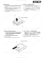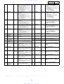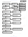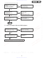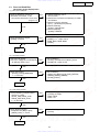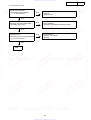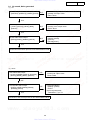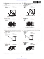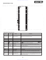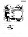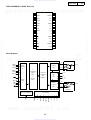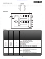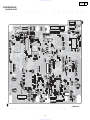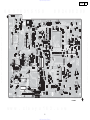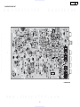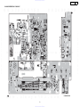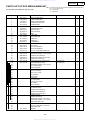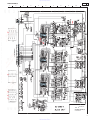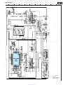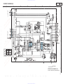
1
http://www.xiaoyu163.com
QQ 376315150 892498299
For U.S.A., Canada, Europe
& Japan model
SERVICE MANUAL
MODEL
Ver. 2
DVD-2900
TEL
TEL
DVD AUDIO-VIDEO / SUPER AUDIO CD PLAYER
13942296513
13942296513
サービスをおこなう前に、このサービスマニュアルを
必ずお読みください。本機は、火災、感電、けがなど
に対する安全性を確保するために、さまざまな配慮を
おこなっており、また法的には「電気用品安全法」に
もとづき、所定の許可を得て製造されております。
従ってサービスをおこなう際は、これらの安全性が維
持されるよう、このサービスマニュアルに記載されて
いる注意事項を必ずお守りください。
● For purposes of improvement, specifications and
design are subject to change without notice.
● 本機の仕様は性能改良のため、予告なく変更すること
があります。
● 補修用性能部品の保有期間は、製造打切後 8年です。
● Please use this service manual with referring to
the operating instructions without fail.
● 修理の際は、必ず取扱説明書を参照の上、作業を行って
,
ください。
● Some illustrations using in this service manual are
slightly different from the actual set.
● 本文中に使用しているイラストは、説明の都合上現物
と多少異なる場合があります。
www
.
xiaoy u163. com
16-11, YUSHIMA 3-CHOME, BUNKYOU-KU, TOKYO 113-0034 JAPAN
Telephone: 03 (3837) 5321
X0168V.02 DE/CDM 0304
http://www.xiaoyu163.com
376315150 892498299
376315150 892498299
注 意
QQ
QQ
QQ 376315150 892498299
TEL 13942296513
http://www.xiaoyu163.com
DVD-2900
2
QQ 376315150 892498299
SAFETY PRECAUTIONS
The following check should be performed for the continued protection of the customer and service technician.
LEAKAGE CURRENT CHECK
Before returning the unit to the customer, make sure you make either (1) a leakage current check or (2) a line to chassis
resistance check. If the leakage current exceeds 0.5 milliamps, or if the resistance from chassis to either side of the
power cord is less than 460 kohms, the unit is defective.
LASER RADIATION
Do not stare into beam or view directly with optical instruments, class 3A laser product.
TEL
TEL
500V
(1)
QQ 376315150 892498299
(1)
www
xiaoy u163. com
(2)
.
2
http://www.xiaoyu163.com
376315150 892498299
376315150 892498299
(2)
QQ
QQ
TEL 13942296513
13942296513
13942296513
1M
http://www.xiaoyu163.com
DVD-2900
DISASSEMBLY
3
QQ 376315150 892498299
各部のはずしかた
(Follow the procedure below in reverse order when reassembling.)
(組み立てるときは、逆の順序で行ってください。)
1. トップカバーのはずしかた
1. Top Cover
(1) 側面及び上面からねじ 10 本、後ろからねじ 2 本をはず
します。
(2) 左右に少し広げ、矢印の方向にずらしながら、はずし
ます。
(1) Remove 10 screws on the top and both sides, and 2
screws on the rear.
(2) Widen the Top Cover a little laterally, then detach it with
sliding in the arrow direction.
TEL
TEL
TEL 13942296513
www
.
2.1. ディスクトレイが電動でオープンできる場合
(1) トップカバーをはずした状態で作業します。
(2) 電源コードを電源コンセントに差し込み、電源スイッ
チを押し、「OPEN/CLOSE」ボタンを押して、ディスク
トレイをオープンします。
(3) ローダーパネルを矢印の方向に持ち上げ、はずします。
(4) 「OPEN/CLOSE」ボタンを押し、ディスクトレイをク
ローズして、電源コンセントから電源コードを抜きま
す。
(5) フロントパネル内の基板と本体側電源基板を接続シテ
イルワイヤー (CX025,CX061) をはずします。
(6) 上からねじ4本、下からねじ4本をはずし、フロント
パネルを矢印の方向にはずします。
(7) フロントパネル内の基板と本体側メイン基板を接続し
ている FFC(CX171)をはずします。
xiaoy u163. com
3
http://www.xiaoyu163.com
376315150 892498299
376315150 892498299
QQ 376315150 892498299
(1) After removing the Top Cover, proceed as follows.
(2) Plug the power cord to the wall outlet, switch on the power, and press the “OPEN/CLOSE” button to open the
Disc Tray.
(3) Detach the Loader Panel by lifting it in the arrow direction.
(4) Press the “OPEN/CLOSE” button to close the Disc Tray,
then unplug the power cord.
(5) Disconnect the wire (CX025, CX061) connecting the
Front Panel’s P.W.B. and the power PWB in the Chassis.
(6) Remove 4 top screws and 4 bottom screws, then detach
the Front Panel to the arrow direction.
(7) Disconnect the FFC (CX171) connecting the Front Panel’s P.W.B. and the main P.W.B. in the Chassis.
QQ
QQ
2.1. When the Disc Tray can be ejected electrically
13942296513
13942296513
2. フロントパネル、ローダーパネルのはずし
かた
2. Loader Panel, Front Panel
http://www.xiaoyu163.com
DVD-2900
4
QQ 376315150 892498299
2.2. When the Disc Tray cannot be ejected electrically
2.2. ディスクトレイが電動でオープンできない場合
(1) トップカバーをはずした状態で作業します。
(2) メカフィクスブラケットの左側の穴に(−)ドライ
バーをいれ、プレートギアをゆっくり押してディスク
トレイを開きます。
(3) ローダーパネルをはずし、ディスクトレイを閉じます。
(4) 前項 1.2.1. の(5)∼(7)と同様に、フロントパネル
をはずします。
(1) After removing the Top Cover, proceed as follows.
(2) Insert a screwdriver(-) into the left hole of the Mecha. Fix
Bracket, and push the Plate Gear of the DVD Mecha.
slowly to open the Disc Tray.
(3) Remove the Loader Panel, and close the Disc Tray.
(4) Detach the Front Panel following the same steps described on the previous page 1.2.1. (5) - (7).
TEL
TEL
13942296513
13942296513
(1)
(2)
(3)
(4)
3. ビデオ基板のはずしかた
Disconnect 33P FFC (CY331) and 5P connector (CY053).
Remove 2 screws on the Video P.W.B.
Remove 2 screws from the rear.
Detach the Video P.W.B. to the arrow direction.
www
.
(1)
(2)
(3)
(4)
33P FFC(CY331) と 5P コネクター(CY053) をはずします。
基板からねじ 2 本をはずします。
リア側からねじ 4 本をはずします。
ビデオ基板を矢印の方向へはずします。
xiaoy u163. com
4
http://www.xiaoyu163.com
376315150 892498299
376315150 892498299
3. Video P.W.B.
QQ 376315150 892498299
QQ
QQ
TEL 13942296513
http://www.xiaoyu163.com
DVD-2900
5
QQ 376315150 892498299
4. DVD Mecha.
4.DVD メカのはずしかた
(1) Disconnect 27P FFC (CY271) and 13P FFC (CY131)
from the Main P.W.B..
(2) Disconnect 12P connector (CY121) from Power P.W.B..
(3) Remove 4 screws on the DVD Mecha and 2 screws on
the Main P.W.B., then take it off in the arrow direction.
(1) メイン基板からの 13P FFC(CY131) をはずします。
(2) パワー基板からの 12P コネクター(CY121) をはずし
ます。
(3) DVD メカからねじ 4 本、メイン基板からねじ 2 本をは
ずし、矢印の方向へ DVD メカをはずします。
TEL
TEL
5.オーディオ基板 / パワー基板のはずしかた
5.1. オーディオ基板
(1) 4P コネクター(CY041) をはずします。
(2) オーディオ基板からねじ 5 本とリア側からねじ 4 本を
はずします。
5.2. Power P.W.B.
5.2. パワー基板
(1) Remove 5 screws on the Power P.W.B..
(2) Disconnect 2P connector (CX024)
(1) パワー基板からねじ 5 本をはずします。
(2) コネクター(CX024)をはずします。
www
.
xiaoy u163. com
5
http://www.xiaoyu163.com
376315150 892498299
376315150 892498299
QQ 376315150 892498299
TEL 13942296513
(1) Disconnect 4P connector (CY041).
(2) Remove 5 screws on the Audio P.W.B., 4 screws from
the rear.
QQ
QQ
5.1. Audio P.W.B.
13942296513
13942296513
5. Audio P.W.B./Power P.W.B.
http://www.xiaoyu163.com
DVD-2900
6
QQ 376315150 892498299
6. Mecha.Unit
6. メカユニットのはずしかた
(1) Remove 2 screws on the top of the Mecha. Unit, and detach the Guide Clamp Bracket with sliding in the arrow direction.
(2) Solder the short-circuit on the Traverse Unit. (Refer to
“Traverse Unit Disassembly” on the page 7.
(3) Disconnect the wires (CX151, CX241, CX031, CX051)
connecting with the Main PWB.
(4) Turn over the Mecha. Unit/Main PWB assembly, and remove 3 screws.
(1) メカの上からねじ 2 本をはずし、ガイドクランプブラ
ケットを矢印方向にずらしながらはずします。
(2) ドライバーメカのショートサーキットを半田付けしま
す。(トラバースユニットのはずしかた 7 ページ参照)
(3) メイン基板と接続しているワイヤー(CX151, CX241,
CX031, CX051)をはずします。
(4) 一体のメカユニット / メイン基板を裏返し、ねじ 2 本
をはずします。
TEL
TEL
13942296513
13942296513
7. トラバースユニットのはずしかた
Caution: The optical pickup can be damaged easily
by static electricity charged on human body. Take
necessary anti-static measures when repairing
around the optical pickup.
注意:光ピックアップは、人体に帯電した静電気等で
静電破壊することがあります。光ピックアップ周辺を
修理する際は、必要な静電対策を行ってください。
7.1. ガイドクランプブラケットのはずしかた
7.1. Guide Clamp Bracket disassembly
(1) ねじ 2 本をはずします。
(2) ガイドクランプブラケットを矢印方向にとりはずしま
す。
(1) Remove 2 screws.
(2) Remove Guide Clamp Bracket to arrow direction.
www
.
xiaoy u163. com
6
http://www.xiaoyu163.com
376315150 892498299
376315150 892498299
7. Traverse Unit Disassembly
QQ
QQ
QQ 376315150 892498299
TEL 13942296513
http://www.xiaoyu163.com
DVD-2900
7
QQ 376315150 892498299
7.2. Tray disassembly
7.2. トレイのはずしかた
(1) Remove to arrow direction.
(2) Solder the short-circuit (see in the frame).
(1) 矢印方向にとりはずします。
(2) 半田付けショートを行います。(枠内図参照 )
TEL
TEL
13942296513
13942296513
7.3. Traverse Unit disassembly
7.3. トラバースユニットのはずしかた
www
.
(1) メイン基板に接続している 24P FFC(CX241)、15P FFC
(CX151),5P PH ワイヤ(CX051)、3P PH ワイヤ
(CX031) をはずします。
(2) ダンパーを固定しているねじ 4 本をはずします。
(3) トラバースユニットを矢印方向にとりはずします。
xiaoy u163. com
7
http://www.xiaoyu163.com
376315150 892498299
376315150 892498299
QQ 376315150 892498299
(1) Remove 24P FFC (CX241), 15P FFC (CX151), 5P PH
WIRE (CX051) and 3P PH WIRE (CX031) connecting
with from the Main P.W.B..
(2) Remove 4 screws fixing Damper.
(3) Remove Traverse Unit to arrow direction.
QQ
QQ
TEL 13942296513
http://www.xiaoyu163.com
DVD-2900
8
QQ 376315150 892498299
Note for disassembly Traverse Unit
(1) When assembling, reverse the order of the above.
(2) When inserting Tray, confirm boss on Slide Cam set to
ditch of the Tray (Compare with below drawing).
トラバースユニット分解の注意
(1) 組み立てるときは、上記の逆の順序で行ってください。
(2) トレイ組込み時、スライドカムのボスがトレイの溝に
合っているか確認してください。(下図参照)
TEL
TEL
13942296513
13942296513
.
xiaoy u163. com
8
http://www.xiaoyu163.com
376315150 892498299
376315150 892498299
www
QQ 376315150 892498299
QQ
QQ
TEL 13942296513
http://www.xiaoyu163.com
DVD-2900
9
QQ 376315150 892498299
DIAGNOSTICS OF OPTICAL PICKUP 光ピックアップの故障診断とトラバース
AND REPLACING TRAVERSE UNIT
ユニットの交換
Make failure diagnostics of the Optical Pickup as follows.
If the laser drive current becomes more than 1.5 times of the
initial value, the Optical Pickup should be replaced.
The laser drive current is registered on the seal attached to
the rear of the Mecha.Unit.
In case of replacing the Pickup, change the whole part of the
Traverse Unit.
No mechanical adjustment is necessary after the replacement.
次の順序で故障診断を行ってください。
レーザー駆動電流が初期値の 1.5 倍以上になっている場合は
光ピックアップ交換の目安となります。
レーザーの電流初期値は、メカの後部のシール上に記入され
ています。
ピックアップ交換の場合は、トラバースユニット単位での交
換となります。メカの調整は不要です。
TEL
TEL
レーザー駆動電流の確認
HF 波形の確認
(109 ページ参照)
Laser drive current check
HF wave form check
(Refer to page 109)
Present value exceeds the initial value by 1.5 times
現在値が初期値の
1.5 倍になっている
Traverse Unit replacing
(See page 7 for details)
トラバースユニット交換
(詳細は 7 ページ)
Laser current registering after replacement.
www
交換後のレーザー電流記入
xiaoy u163. com
Step: Disc playback
Write the measured value on the seal attached to the
Mecha. Unit
.
手順 :ディスクを再生
その時の Iop 値をメカ後方のシールの上に重ねて貼る
等で更新する。
*Iop の測定方法は、10,11 ページ参照。
*As to the measuring method, refer to page 10,11.
9
http://www.xiaoyu163.com
376315150 892498299
376315150 892498299
QQ 376315150 892498299
TEL 13942296513
QQ
QQ
ディスクを読み込まない
スムーズに再生しない、等
Disc no read,unsteady playback, etc.
13942296513
13942296513
Example: DVD 30mA
例: CD 30mA
http://www.xiaoyu163.com
DVD-2900
10
QQ 376315150 892498299
1. Label Indication of DVD Mechanism.
1. DVD メカのラベル表示
Laser current consumption value
ex) DVD *** mA, CD *** mA
レーザー駆動電流値
例)DVD *** mA, CD *** mA
TEL
TEL
2. レーザーピックアップの取扱注意
3. Replacement of the Laser Pick-up
(Traverse Unit)
3. レーザーピックアップ ( トラバースユニッ
ト ) の交換
Check the Iop(Laser drive current)
If the present Iop (current) value exceeds.+50% of the initial value, replace the Traverse unit(Laser Pick-up) with a
new one.
Iop( レーザー駆動電流)をチェックします。
現在の Iop 値が初期値の 50%を越えている場合、トラ
バースユニット(レーザーピックアップ)を交換してく
ださい。
4. Iop Measurement Method
4. Iop の測定方法
When measuring Laser drive current (Iop), playback the
discs (CD,DVD) described below, measure Iop for CD
Laser and DVD Laser by the test point (+5V-A2 -LD(CD),LD(DVD))on the Main P.W.B.
Test Disc :DVD/DVDT-S01 or commercially available discs.
:CD/TCD-784 (manufactured by ALMEDIO INC)
or commercially available discs.
www
.
レ ー ザ ー 駆 動 電 流 を 測 定 す る 場 合、下 記 の デ ィ ス ク
(CD,DVD) を再生します。
Main基板上のテストポイント(+5V-A2∼LD(CD),LD(DVD))
にて、CD レーザーと DVD レーザーの Iop を測定してく
ださい。
xiaoy u163. com
テストディスク:DVD/DVDT-S01 または市販同等ディス
ク
:CD/TCD-784(ALMEDIO 社製)または
市販同等ディスク
10
http://www.xiaoyu163.com
376315150 892498299
376315150 892498299
QQ 376315150 892498299
TEL 13942296513
QQ
QQ
レーザーダイオードの破壊防止。
光素子ユニットを交換するときは、以下を遵守してくださ
い。
(1) 光素子ユニットの接続ケーブルをはずすときは、静電対
策を行ったデスク上で作業してください。
(2) 作業者は、リストストラップを使用してください。
(3) レーザーダイオードの破壊防止のため、24P FFC ケーブ
ルをはずす前にランドを半田付けショートしてくださ
い。
(4) 光素子ユニットのコネクタ部に触れないでください。
the protection for the damage of laser diode.
If you want to change the optical device unit from any other
units, you must keep the following.
(1) It should be done at the desk already took measures the
static electricity in care of removing the OPU's (Optical
device unit) connector cable.
(2) Workers should be put on the "Earth Band".
(3) It should be done to add the solder to the short land to
prevent the broken Laser diode before removing the 24P
FFC cable.
(4) Don't touch OPU's connector parts carelessly.
13942296513
13942296513
2. Note for Handling the Laser Pick-Up
http://www.xiaoyu163.com
DVD-2900
11
QQ 376315150 892498299
4.1. DVD Laser current measurement
4.1. DVD レーザー電流測定
LD(DVD)
LD(DVD)
+5V-A2
+5V-A2
Oscilloscope
Oscilloscope
(1) Connect the oscilloscope to +5V-A2 of test point for GND
side and LD(DVD) of test point for signal side.
(2) Playback the title 1 / chapter 1 of the DVD Test Disc.
(3) Measure the voltage between +5V-A2 and LD(DVD), calculate Iop by the formula as shown below.
(1) オシロスコープをテストポイント +5V-A2(GND) と
LD(DVD)( 信号 ) へ接続します。
(2) DVD テストディスクのタイトル 1・チャプター 1 を再生
します。
(3) +5V-A2 と LD(DVD) 間の電圧を測定し、次式により Iop を
算出します。
Measurement Voltage Value
Iop = ----------------------------------------------------------------------------14 (Resistance value)
測定電圧値
Iop = ----------------------------14(抵抗値)
TEL
TEL
(1) オシロスコープをテストポイント
+5V-A2(GND) と
LD(CD)( 信号 ) へ接続します。
(2) CD テストディスクのトラック 1 を再生します。
(3) +5V-A2 と LD(CD) 間の電圧を測定し、次式より Iop を算
出します。
(1) Connect the oscilloscope to +5V-A2 of test point for GND
side and LD(CD) of test point for signal side.
(2) Playback the track 1 of the CD Test Disc.
(3) Measure the voltage between +5V-A2 and LD(CD), calculate Iop by the formula as shown below.
www
.
xiaoy u163. com
LD(DVD)
LD(CD)
+5V-A2
Main Unit foil side
11
http://www.xiaoyu163.com
376315150 892498299
376315150 892498299
QQ 376315150 892498299
TEL 13942296513
QQ
QQ
測定電圧値
Iop = -----------------------------------11.75(抵抗値)
Measurement Voltage Value
Iop = ----------------------------------------------------------------------------11.75 (Resistance value)
13942296513
13942296513
4.2. CD レーザー電流測定
4.2. CD Laser current measurement
http://www.xiaoyu163.com
DVD-2900
12
QQ 376315150 892498299
5. Optical Pick-up Diagnostics and Replacement
When repairing, carry out failure diagnostics by following the
procedure described below.
If the present value of the laser drive current is 50% up to initial value, it is the point of the pickup replacement.
In case of the pickup replacement, replace the Traverse Unit
with no adjustment.
The initial value is indicated on the label on back side of
Mecha.
5. 光ピックアップ診断と交換
交換時、以下の手順で故障診断を行ってください。
レーザー駆動電流の現在値が初期値の 50%以上なら、
ピックアップを交換すべきです。
ピックアップ交換の場合はトラバースユニットを交換し、
調整は不要です。
初期値は、メカ後部のラベルに表示されています。
Laser drive current check
HF signal check
レーザー駆動電流のチェック
HF 信号チェック
TEL
”NO DISC ”表示、再生不良等
TEL
NO DISC indicated, Playback not smooth,etc.
現在値:
初期値の 50%以上
トラバースユニット交換
( 6 ページ参照)
Laser drive current check after replacement.
If the present value is less than 80mA, write on
the new label by hand, put on the new label over
the old label.
交換後、レーザー駆動電流をチェックします。
現在値が 80mA 以下なら新ラベル上へ手書きし、
旧ラベルの上に貼り付けます。
If the present value exceeds 80mA, replace the Traverse Unit
a new one.
Cause: Damaged electrostatically when replaced.
www
.
現在値が 80mA 以上なら、再度トラバースユニットを交換し
てください。
原因 :交換時、静電破壊された。
xiaoy u163. com
12
http://www.xiaoyu163.com
376315150 892498299
376315150 892498299
Traverse Unit replacement
(refer to page 6)
QQ
QQ
QQ 376315150 892498299
TEL 13942296513
13942296513
13942296513
Present value:
50% up to initial value
http://www.xiaoyu163.com
DVD-2900
SERVICE MODE
13
QQ 376315150 892498299
サービスモードについて
1. Aging Mode
1. エージングモード
(1) preparation
(a) Equipment used: Any one of DVD Karaoke Disc (containing more than 10 titles).
(b) Unit setting : No spec other than the following procedure
(Aging mode).
At the tray open status, press the “POWER” button to
turn on the power while pressing the “PLAY” and
“OPEN/CLOSE” buttons for DVD operation simultaneously.
mark on the FL lights, and the unit is set
to the heat run mode.
(2) procedure
FL display
エラー内容
FL 管表示
1
不良ディスク
ERROR 02
2
フォーカスエラー
ERROR 02
3
リードエラー
ERROR 02
ERROR 04
4
トラッキングエラー
ERROR 04
Tray Error
ERROR 05
5
トレイエラー
ERROR 05
Navigation Pack Read Error
ERROR 06
6
ナビゲーションパックエラー
ERROR 06
Bad Disc
ERROR 02
2
Focus Error
ERROR 02
3
Read Error
ERROR 02
4
Tracking Error
5
6
QQ 376315150 892498299
2. 初期設定モード
2. Initial Setting Mode
(1) Preparation
(1) 準備
(a) Equipment used: None
(b) Unit setting: No spec other than the following procedure
(2) Procedure
(a) Initialize the DVD player when µcom, peripheral parts of
µcom, or Main P.W.B. has been replaced in servicing.
(b) Carry out the following to restore factory setting mode. At
the player stop condition, press 3 buttons for DVD operation(“PLAY”,”OPEN/CLOSE”, and “
SKIP”) until
“INITIALIZE” appears and disappears in the FL.
(“Initialized” appears and disappears on the TV screen.)
(c) All user setting will be lost and its factory setting will be
restored when this initialization is made. Be sure to memorize your setting for restoring again after the initialization.
www
.
(a) 使用機器:無
(b) 本体設定:下記手順以外規定無。
(2) 手順
(a) サービスにて、マイコンやマイコン周辺部分やメイン
基板を交換した場合は、DVD プレーヤーの初期化を
行ってください。
(b) セットの初期化を下記の手順で行い、工場出荷モード
に設定する。
セットが停止状態にて、DVD 操作部の「再生ボタ
ン」+「開 / 閉ボタン」+「
( スキップ)ボタン」
の 3 重押しを FL 管に "INITIALIZE" が表示され消える
まで押します。(TV 画面には”初期化しました”が
表示され消えます。)
(c) 初期化を行うとお客様が設定した内容が工場出荷状態
に戻りますので、あらかじめ設定内容を控えておき初
期化後に再設定してください。
xiaoy u163. com
13
http://www.xiaoyu163.com
376315150 892498299
376315150 892498299
TEL 13942296513
QQ
QQ
No.
1
13942296513
13942296513
(a) 上記手順でエージングモードに設定する。
(b) トレイに DVD カラオケディスクを入れ、「再生ボタン」
を 2 回押して、FL 管の
マークが点滅になると、
「ディスクのタイトル 1 とタイトル 10 を再生した後、
トレイを自動で開 / 閉し、再度タイトル 1 の再生を行
う。」エージング動作になります。停止させるか、エ
ラーにて停止するまでこの動作を自動で繰り返します。
DVD 部にエラーが発生した場合は、FL 管に下表のエ
ラーが表示されます。
TEL
TEL
Error contents
(a) 使用機器:DVD カラオケディスク(10 タイトル以上
の物)。
(b) 本体設定:下記設定以外規定無。
(エージングモード)
トレイを開けた状態で DVD ユニットの「再生ボタン」
+「開 / 閉ボタン」を同時に押しながら「電源ボタン」
を押してセットの電源を入れると、FL 管の
マー
クが点灯し、ヒートランモードに設定される。
(2) 手順
(a) According the above, set to the aging mode.
(b) Set a DVD Karaoke disc to the tray and press the “PLAY”
button twice.
mark on the FL blinks, and aging
operation(after playback title-1 and title-10 of the disc,
the tray open/close is made automatically, then playback
the title-1 again) starts. This aging operation continues
automatically until it is stopped or it stops caused by an
error.In case of some error in DVD, the following error
messages are displayed on the FL.
No
(1) 準備
http://www.xiaoyu163.com
DVD-2900
14
QQ 376315150 892498299
3. μ-Com Firm Check Mode
3.マイコンファームチェックモード
(1) Preparation
(a) Equipment used: None
(b) Unit setting: No spec other than the following procedure.
(2) Procedure
Ver.030307
(Display)
030307
Ver.6237
(Display)
6237
Panel µcom
セットのシ
リアル番号
(下5桁)
Ver.6236
(Display)
6236
1
2
B/Eマイコン
パネルマイコン
Ver.030307
( 表示 )030307
Ver.6237
( 表示 )6237
Ver.6236
( 表示 )6236
2
3
3
4
.
QQ 376315150 892498299
xiaoy u163. com
14
http://www.xiaoyu163.com
376315150 892498299
376315150 892498299
TEL 13942296513
QQ
QQ
4
www
00001 ∼
ドライブマイコン
13942296513
13942296513
00001-
B/E µcom
(a) DVD 操作部の「再生ボタン」と「開 / 閉ボタン」を
押しながらセットの「電源ボタン」を押し電源を入れ
ます。
(b) FL 管全点灯モード。
FL 管の故障判別用のモードで、リモコンの「スティ
ル / ポーズ
ボタン」を押すと FL 管が全点灯し
ます。
(c) DVD マイコン及び本体マイコンのファーム確認モー
ド
搭載されている各マイコンのファーム状態を表示しま
す。
・ DVD マイコンのファーム:リモコンの「メニューボタ
ン」または
、
ボタンを押します。
・ リモコンのメニューボタンまたは
、
ボタン
を押すたびにマイコンファームを次々と表示します。
表示例:〔DRV 030307 、 B/E 6237 、 PANEL 6236〕
TEL
TEL
1
Drive µcom
(a) 使用機器:無
(b) 本体設定:下記手順以外規定無。
(2) 手順
(a) Press the “POWER” button to turn on the power while
pressing the “PLAY” and “OPEN/CLOSE” buttons for
DVD operation simultaneously.
(b) FL all light mode.
This mode is for detecting FL defects. Press “STILL/
PAUSE
” on the remote control unit once to light
all FL segments.
(c) DVD µcom and main unit µcom firm check mode. This
mode is for displaying the status of each µcom employed.
• DVD µcom firm: Press the “MENU” button or
,
button.
• Each time the “MENU” button or
,
button on the remote control unit is pressed, µcom firm
is displayed one after another.
Ex.: [DRV 030307, B/E 6237,PANEL 6236]
Set Serial No.
(lower 5 digits)
(1) 準備
http://www.xiaoyu163.com
15
DVD-2900
QQ 376315150 892498299
4. Setting up the test mode
4. テストモード
(1) Setting up
• In order to set up the test mode, you press STOP button
and REV button simultaneously in the heat-run mode.Fundamentaly, you can set up the test mode at the stop state
after disc loading. (Heat-run mode is set up by pressing
PLAY button,holding OPEN/CLOSE button. If it becomes
heat run mode, PLAY indicator and PAUSE indicator will
light up.)
(1) テストモードへの投入
・ テストモードへの投入はヒートランモード時に
STOP
キーと REV キーを 2 重押しすることで行う。基本的に
ディスクローディング後の停止状態でテストモードに
投入する。( ヒートランモードへの投入は OPEN/CLOSE
キーと PLAY キーを 2 重押しすることで行う。ヒートラ
ンモードになると PLAY インジケータと PAUSE インジ
ケータが点灯する。
)
LOADING 表示
LOADING display
↓
FL display (The display part of 13 digits)
1
2
3
4
5
6
7
8
↓
FL 管の表示 (13 桁の表示部 )
9
10
11
12
1
13
2
3
4
5
6
7
8
9
10
11
12
13
T
T
(2) Mode Select
(2) モードの選択
FL 管の表示 (13 桁の表示部 )
FL display (The display part of 13 digits)
1
2
T
3
3
4
5
6
7
8
9
10
11
12
13
4
5
6
7
8
9
10
11
12
4
5
6
7
8
9
10
11
12
13
13
1
2
T
7
3
4
5
6
7
8
9
10
11
12
13
7
(3) モードの確定
・ モードを選択してある状態で PLAY キーを押すとモード
を確定する。
(a) サーボ調整値表示モードの場合は、フォーカスオフ
セット調整値を表示する。
• The mode will be decided if the PLAY button is pushed in
the state where the mode is chosen.
(a) In the case of servo adjustment value display mode, a
focus offset adjustment value is displayed.
FL 管の表示 (13 桁の表示部 )
FL display (The display part of 13 digits)
1
2
3
4
5
6
7
8
9
10
11
12
13
1
2
3
4
5
6
7
8
9
10
11
12
13
T
3
1
n
n
n
n
n
n
n
n
n
n
T
3
1
n
n
n
n
n
n
n
n
n
n
(n: 調整値 )
(b) トレースモード ( エラーレート表示 ) の場合は、1層
内周のトレースを選択する。
(n:adjustment value)
(b) In the case of trace mode (error rate display), trace of
the circumference in one layer is chosen.
FL 管の表示 (13 桁の表示部 )
FL display (The display part of 13 digits)
1
2
3
4
5
6
7
8
9
10
11
12
13
1
2
3
4
5
6
7
8
9
10
11
12
13
T
7
1
F
F
F
F
F
F
F
F
F
F
T
7
1
F
F
F
F
F
F
F
F
F
F
(F: アドレス及びエラーレートは未確定時、F を表示する。)
(F: An address and an error rate display F at the time of undecided.)
(4) モード内での変更
(4) Change within the mode
• If the REV button or the FWD button is pushed in the state
where the mode is decided, a change within the mode will
be made.
(a) In the case of servo adjustment value display mode (refer to table 1 servo adjustment value display mode details)
www
T
FL 管の表示 (13 桁の表示部 )
1
2
3
4
5
6
7
8
9
10
11
12
13
T
X
X
n
n
n
n
n
n
n
n
n
n
xiaoy u163. com
FL display (The display part of 13 digits)
1
・ モードを確定してある状態で REV キー又は FWD キーを
押すとモード内での変更を行う。
(a) サーボ調整値表示モードの場合( 表1サーボ調整値表
示モード詳細 参照)
2
3
4
5
6
X
X
n
n
n
(XX: 選択モード [31 ∼ 62]、n: 調整値 )
7
8
9
10
11
12
13
n
n
n
n
n
n
n
(XX:selection mode [31--62] n:adjustment value)
.
15
http://www.xiaoyu163.com
376315150 892498299
376315150 892498299
QQ 376315150 892498299
TE
L 13942296513
(3) Mode decision
T
3
QQ
QQ
3
3
FL 管の表示 (13 桁の表示部 )
FL display (The display part of 13 digits)
2
2
T
(b) 再度 REV キー又は FWD キーを押すとトレースモード
( エラーレート表示 ) になる。
(b) If the REV button or the FWD button is pushed again, it
will become the trace mode (error rate display).
1
1
13942296513
13942296513
・ モードには、サーボ調整値表示モードとトレースモード
( エラーレート表示 ) の 2 つがある。
(a) テストモード投入後に REV キー又は FWD キーを押す
と、サーボ調整値表示モードになる。
TEL
TEL
• There are two, servo adjustment value display mode and
trace mode (error rate display), in the mode.
(a) If the REV button or the FWD button is pushed in the test
mode, it will become servo adjustment value display
mode.
http://www.xiaoyu163.com
16
DVD-2900
QQ 376315150 892498299
(b) In the case of trace mode (error rate display) (refer to table 2 trace mode details)
(b) トレースモード ( エラーレート表示 ) の場合( 表 2 ト
レースモード詳細 参照)
FL display (The display part of 13 digits)
FL 管の表示 (13 桁の表示部 )
1
2
3
4
5
6
7
8
9
10
11
12
13
1
2
3
4
5
6
7
8
9
10
11
12
13
T
Y
Y
F
F
F
F
F
F
F
F
F
F
T
Y
Y
F
F
F
F
F
F
F
F
F
F
(YY: select mode [71--94] ,F: address and an error rate display F at the
time of undecided)
(YY: 選択モード [71 ∼ 94]、F: アドレス及びエラーレートは未確定
時、F を表示する。)
(5) Execution of trace mode (error rate display)
(refer to table 2 trace mode details)
(5) トレースモード ( エラーレート表示 ) の実行(
表 2 トレースモード詳細 参照)
• Trace will be performed if the PLAY button is pushed after
choosing operation.
・ 動作を選択した後、PLAY キーを押すとトレースを実行
する。
FL display (The display part of 13 digits)
FL 管の表示 (13 桁の表示部 )
1
2
3
4
5
6
7
8
9
10
11
12
13
1
2
3
4
5
6
7
8
9
10
11
12
13
T
Y
Y
m
m
m
m
m
m
l
l
l
l
T
Y
Y
m
m
m
m
m
m
l
l
l
l
• The mode chosen when selection mode was changed into
the trace execution and the PLAY button was pushed is
performed from the beginning.When the PLAY button is
pushed without changing selection mode, the mode under
selection is performed from the beginning.(If the PLAY
button is pushed, the address corresponding to the chosen mode will be searched again.)
(PLAY キーを押したら、選択しているモードに対
応したアドレスを再度サーチする。)
(6) Other operation
FL display (The display part of 13 digits)
1
2
3
4
5
6
7
8
9
10
11
(a) サーボ調整値表示モード、トレースモード ( エラー
レート表示 ) 中に STOP キーを押すとテストモード投
入時の状態に戻る。
QQ 376315150 892498299
FL 管の表示 (13 桁の表示部 )
12
13
T
(b) Push the OPEN/CLOSE button twice and carry out servo readjustment in OPEN operation ->CLOSE operation.
(It readjusts with test mode.)
1
T
↓
LOADING display
3
5
6
7
8
9
10
11
12
13
FL 管の表示 (13 桁の表示部 )
FL display (The display part of 13 digits)
2
4
OPEN 表示
↓
CLOSE 表示
↓
LOADING 表示
↓
CLOSE display
1
3
(b) OPEN/CLOSE キーを 2 回押して、OPEN 動作→ CLOSE
動作で、サーボ再調整する。
( テストモードのまま再調整する。)
OPEN display
↓
↓
2
4
5
6
7
8
9
1
10
11
12
(c) By pressing STOP button and REV button simultaneously in the test mode, it returns to heat-run mode.
.
3
4
5
6
7
8
9
10
11
12
13
(c) テストモード中に STOP キーと REV キーの 2 重押し
( 投入時と同じキー ) で、ヒートランモードに戻る。
T
www
2
T
13
xiaoy u163. com
16
http://www.xiaoyu163.com
376315150 892498299
376315150 892498299
TEL 13942296513
(6) その他の動作
QQ
QQ
(a) If the STOP button is pushed into servo adjustment value display mode and trace mode (error rate display), it
will return to the state at the time of a test mode injection.
13942296513
13942296513
(YY: 選択モード [71 ∼ 94]、m: アドレス [PBA][HEX]、
l: エラーレート [COUNT/SEC][HEX])
( 注 )CD:300 フレーム ,DVD:85ECC ブロック毎にデータ
更新する。
・ トレース実行中に選択モードを変更し、PLAY キーを押
すと選択したモードを最初から実行する。選択モードを
変更せずに PLAY キーを押した場合も、選択中のモード
を最初から実行する。
TEL
TEL
(YY:select mode[71--94],m:address[PBA][HEX],
l:error rate[COUNT/SEC][HEX])
(Note) Renewal of data is carried out for every CD:300 frame and
DVD:85ECC block.
http://www.xiaoyu163.com
DVD-2900
(7) Test mode detailed table
17
QQ 376315150 892498299
(7) テストモード詳細一覧表
Table 1: servo adjustment value display mode details
XX
Contents
Contents
suppleme
nt
31
RFP FE Offset
32
RFP TE
Gain
表 1 サーボ調整値表示モード詳細
layer 0
PI of CXD1881AR An offset value and
FE An offset value is displayed.
Pi offset is shown in higher rank
1Byte.
FE offset is shown in low rank 1Byte.
31
RFP FE Offset
レイヤ 0
CXD1881AR の PI オフセット値と FE
オフセット値を表示。
上位 1Byte に Pi オフセットを示す。
下位 1Byte に FE オフセットを示す。
Bal
layer 0
TE balance gain value of CXD1881AR
is displayed.
32
RFP TE
Gain
Bal
レイヤ 0
CXD1881ARのTE バランスゲイン値を
表示す。
33
RFP TE Output
Gain
layer 0
TE output gain value of CXD1881AR is
displayed.
33
RFP TE Output
Gain
レイヤ 0
CXD1881ARのTE 出力ゲイン値を表示
す。
34
RFP TE Offset
layer 0
TE offset value of CXD1881AR is
displayed.
34
RFP TE Offset
レイヤ 0
CXD1881AR の TE オフセット値を表
示。
35
DSP TE Offset
layer 0
TE offset value inside CXD1885Q is
displayed.
35
DSP TE Offset
レイヤ 0
CXD1885Q 内部の TE オフセット値を
表示。
36
Fcs Bias
layer 0
The focus bias value
CXD1885Q is displayed.
inside
36
Fcs Bias
レイヤ 0
CXD1885Q 内部のフォーカスバイア
ス値を表示。
37
Fcs AGC
layer 0
The inside focus gain (setting 0x2000
to 1) value of CXD1885Q is
displayed.。
Therefore, 0x1FF2 and in the case of
0x2012, it is as follows.
0x1FF2(8178) / 0x2000(8192) =
0.998291015625(fold)
0x2012(8210) / 0x2000(8192) =
1.002197265625(fold)
Notes: The inside of ( ) is a decimal
system equivalent.
37
Fcs AGC
レイヤ 0
CXD1885Q 内 部 フ ォ ー カ ス ゲ イ ン
(0x2000 を 1 として ) 値を表示。
0x1FF2 や 0x2012 の場合、以下のよ
うになる。
0x1FF2(8178) / 0x2000(8192) =
0.998291015625( 倍 )
0x2012(8210) / 0x2000(8192) =
1.002197265625( 倍 )
注 :( ) 内は 10 進換算値
38
Trk AGC
layer 0
The inside tracking gain (setting
0x2000 to 1) value of CXD1885Q is
displayed.。
Therefore, 0x1FF2 and in the case of
0x2012, it is as follows.
0x1FF2(8178) / 0x2000(8192) =
0.998291015625(fold)
0x2012(8210) / 0x2000(8192) =
1.002197265625(fold)
Notes: The inside of ( ) is a decimal
system equivalent
38
Trk AGC
レイヤ 0
CXD1885Q内部トラッキングゲイン(0
x2000 を 1 として ) 値を表示。
0x1FF2 や 0x2012 の場合、以下のよ
うになる。
0x1FF2(8178) / 0x2000(8192) =
0.998291015625( 倍 )
0x2012(8210) / 0x2000(8192) =
1.002197265625( 倍 )
注 :( ) 内は 10 進換算値
39
Pi Offset
layer 0
It is the parameter calculated inside
CXD1885Q.
The value displayed on a set serves as
the number of complement of 2 of
2Bytes(es) doubled 256.
A voltage value is 6.25mV per bit.
39
Pi Offset
レイヤ 0
CXD1885Q 内 部 で 計 算 さ れ る パ ラ
メータ。
セットに表示される値は、256 倍され
た 2Bytes の 2 の補数となる。
電圧値は 1bit あたり 6.25mV。
40
FE Offset
layer 0
It is the parameter calculated inside
CXD1885Q.
The value displayed on a set serves as
the number of complement of 2 of
2Bytes(es) doubled 256.
A voltage value is 6.25mV per bit.
40
FE Offset
レイヤ 0
CXD1885Q 内 部 で 計 算 さ れ る パ ラ
メータ。
セットに表示される値は、256 倍され
た 2Bytes の 2 の補数となる。
電圧値は 1bit あたり 6.25mV。
41
SE Offset
layer 0
It is the parameter calculated inside
CXD1885Q.
The value displayed on a set serves as
the number of complement of 2 of
2Bytes(es) doubled 256.
A voltage value is 6.25mV per bit.
41
SE Offset
レイヤ 0
CXD1885Q 内 部 で 計 算 さ れ る パ ラ
メータ。
セットに表示される値は、256 倍され
た 2Bytes の 2 の補数となる。
電圧値は 1bit あたり 6.25mV。
42
RFP FE Offset
layer 1
PI of CXD1881AR An offset value and
FE An offset value is displayed.
Pi offset is shown in higher rank
1Byte.
FE offset is shown in low rank 1Byte.
42
RFP FE Offset
レイヤ 1
CXD1881AR の PI オフセット値と FE
オフセット値を表示。
上位 1Byte に Pi オフセットを示す。
下位 1Byte に FE オフセットを示す。
43
RFP TE
Gain
Bal
layer 1
TE balance gain value of CXD1881AR
is displayed.
43
RFP TE
Gain
Bal
レイヤ 1
CXD1881ARのTE バランスゲイン値を
表示。
44
RFP TE Output
Gain
layer 1
TE output gain value of CXD1881AR is
displayed.
44
RFP TE Output
Gain
レイヤ 1
CXD1881AR の TE 出力ゲイン値を表
示。
45
RFP TE Offset
layer 1
TE offset value of CXD1881AR is
displayed.
45
RFP TE Offset
レイヤ 1
CXD1881AR の TE オフセット値を表
示。
46
DSP TE Offset
layer 1
It is the parameter calculated inside
CXD1885Q.
The value displayed on a set serves as
the number of complement of 2 of
2Bytes(es) doubled 256.
A voltage value is 6.25mV per bit.
46
DSP TE Offset
レイヤ 1
CXD1885Q 内 部 で 計 算 さ れ る パ ラ
メータ。
セットに表示される値は、256 倍され
た 2Bytes の 2 の補数となる。
電圧値は 1bit あたり 6.25mV。
47
Fcs Bias
layer 1
It is the parameter calculated inside
CXD1885Q.
The value displayed on a set serves as
the number of complement of 2 of
2Bytes(es) doubled 256.
A voltage value is 6.25mV per bit.
47
Fcs Bias
レイヤ 1
CXD1885Q 内 部 で 計 算 さ れ る パ ラ
メータ。
セットに表示される値は、256 倍され
た 2Bytes の 2 の補数となる。
電圧値は 1bit あたり 6.25mV。
13942296513
QQ
376315150 892498299
TEL 13942296513
www
.
QQ 376315150 892498299
xiaoy u163. com
17
http://www.xiaoyu163.com
376315150 892498299
内容説明
QQ
内容補足
13942296513
内容
TEL
XX
TEL
Contents explanation
http://www.xiaoyu163.com
DVD-2900
18
QQ 376315150 892498299
48
Fcs AGC
レイヤ 1
CXD1885Q 内 部 フ ォ ー カ ス ゲ イ ン
(0x2000 を 1 として ) 値を表示。
0x1FF2 や 0x2012 の場合、以下のよ
うになる。
0x1FF2(8178) / 0x2000(8192) =
0.998291015625( 倍 )
0x2012(8210) / 0x2000(8192) =
1.002197265625( 倍 )
注 :( ) 内は 10 進換算値
49
Trk AGC
layer 1
The inside tracking gain (setting
0x2000 to 1) value of CXD1885Q is
displayed.
Therefore, 0x1FF2 and in the case of
0x2012, it is as follows.
0x1FF2(8178) / 0x2000(8192) =
0.998291015625(fold)
0x2012(8210) / 0x2000(8192) =
1.002197265625(fold)
Notes: The inside of ( ) is a decimal
system equivalent
49
Trk AGC
レイヤ 1
CXD1885Q 内部トラッキングゲイン
(0x2000 を 1 として ) 値を表示。
0x1FF2 や 0x2012 の場合、以下のよ
うになる。
0x1FF2(8178) / 0x2000(8192) =
0.998291015625( 倍 )
0x2012(8210) / 0x2000(8192) =
1.002197265625( 倍 )
注 :( ) 内は 10 進換算値
50
Pi Offset
layer 1
It is the parameter calculated inside
CXD1885Q.
The value displayed on a set serves as
the number of complement of 2 of
2Bytes(es) doubled 256.
A voltage value is 6.25mV per bit.
50
Pi Offset
レイヤ 1
CXD1885Q 内 部 で 計 算 さ れ る パ ラ
メータ。
セットに表示される値は、256 倍され
た 2Bytes の 2 の補数となる。
電圧値は 1bit あたり 6.25mV。
51
FE Offset
layer 1
It is the parameter calculated inside
CXD1885Q.
The value displayed on a set serves as
the number of complement of 2 of
2Bytes(es) doubled 256.
A voltage value is 6.25mV per bit.
51
FE Offset
レイヤ 1
CXD1885Q 内 部 で 計 算 さ れ る パ ラ
メータ。
セットに表示される値は、256 倍され
た 2Bytes の 2 の補数となる。
電圧値は 1bit あたり 6.25mV。
52
SE Offset
layer 1
It is the parameter calculated inside
CXD1885Q.
The value displayed on a set serves as
the number of complement of 2 of
2Bytes(es) doubled 256.
A voltage value is 6.25mV per bit.
52
SE Offset
レイヤ 1
CXD1885Q 内 部 で 計 算 さ れ る パ ラ
メータ。
セットに表示される値は、256 倍され
た 2Bytes の 2 の補数となる。
電圧値は 1bit あたり 6.25mV。
53
PO error
detection
number
Error rate
It is invalid at the time of CD
operation.
53
PO 誤り検出数
エ ラ ー
レート
CD 時は無効。
54
PO uncorrectable error
number
Error Rate
It is invalid at the time of CD
operation.
54
PO 訂正不可数
エ ラ ー
レート
CD 時は無効。
55
PI error detection number
Error Rate
CD : C1 error detection number
55
PI 誤り検出数
エ ラ ー
レート
CD 時は C1 誤り検出数。
56
PI uncorrectable
error
number
Error Rate
CD : C2 uncorrectable error number
56
PI 訂正不可数
エ ラ ー
レート
CD 時は C2 訂正不可数。
57
Mirr Count
Disc discriminant
They are the contents at the time of
disk distinction.
Please refer to "Table 3 Disc
distinction information" about the
contents of a value.
57
Mirr Count
ディスク
判別
ディスク判別時の内容。
値の内容は「表3ディスク判別情報」
を参照。
58
Mirr Width
Disc discriminant
They are the contents at the time of
disk distinction.
Please refer to "Table 3 Disc
distinction information" about the
contents of a value.
58
Mirr Width
ディスク
判別
ディスク判別時の内容。
値の内容は「表3ディスク判別情報」
参照。
59
FZC Count
Disc discriminant
They are the contents at the time of
disk distinction.
Please refer to "Table 3 Disc
distinction information" about the
contents of a value.
59
FZC Count
ディスク
判別
ディスク判別時の内容。
値の内容は「表3ディスク判別情報」
参照。
60
Pi Level
Disc discriminant
They are the contents at the time of
disk distinction.
Please refer to "Table 3 Disc
distinction information" about the
contents of a value.
60
Pi Level
ディスク
判別
ディスク判別時の内容。
値の内容は「表3ディスク判別情報」
参照。
61
Disc Type
Disc Type
They are the contents at the time of
disk type.
Please refer to "Table 4 Disc
classification information" about the
contents of a value.
61
Disc Type
ディスク
種別
ディスク種別の内容。
値の内容は「表4ディスク種別情報」
参照。
62
PO error
detection
number and
address
Error rate
PO error detection number is invalid
at the time of CD operation.
62
PO 誤り検出数
とアドレス
エラー
レート
CD 時は PO 誤り検出数は無効。
TEL 13942296513
www
.
QQ 376315150 892498299
xiaoy u163. com
18
http://www.xiaoyu163.com
376315150 892498299
376315150 892498299
The inside focus gain (setting 0x2000
to 1) value of CXD1885Q is displayed.
Therefore, 0x1FF2 and in the case of
0x2012, it is as follows.
0x1FF2(8178) / 0x2000(8192) =
0.998291015625(fold)
0x2012(8210) / 0x2000(8192) =
1.002197265625(fold)
Notes: The inside of ( ) is a decimal
system equivalent.
QQ
QQ
layer 1
13942296513
13942296513
Fcs AGC
TEL
TEL
48
http://www.xiaoyu163.com
DVD-2900
19
QQ 376315150 892498299
Table 2: trace mode details
YY
表 2 トレースモード詳細
Contents
Contents supplement
YY
内容
補足説明
1 層内周の PO 誤り検出数とアド
レスの表示
CD 時は無効。
A display of PO uncorrectable
number of the inner circumference of 1-layer and an address.
It is invalid at the time of CD
operation.
72
1 層内周の PO 訂正不可数とアド
レスの表示
CD 時は無効。
73
A display of PI error detection
number of the inner circumference of 1-layer and an address.
CD : C1 error detection number
73
1 層内周の PI 誤り検出数とアドレ
スの表示
CD 時は C1 誤り検出数。
74
A display of PI uncorrectable
number of the inner circumference of 1-layer and an address.
CD : C2 uncorrectable error
number
74
1 層内周の PI 訂正不可数とアドレ
スの表示
CD 時は C2 訂正不可数。
75
A display of PO error detection
number of the central circumference of 1-layer and an address.
It is invalid at the time of CD
operation.
75
1 層中周の PO 誤り検出数とアド
レスの表示
CD 時は無効。
76
A display of PO uncorrectable
number of the central circumference of 1-layer and an address.
It is invalid at the time of CD
operation.
76
1 層中周の PO 訂正不可数とアド
レスの表示
CD 時は無効。
77
A display of PI error detection
number of the central circumference of 1-layer and an address.
CD : C1 error detection number
77
1 層中周の PI 誤り検出数とアドレ
スの表示
CD 時は C1 誤り検出数。
78
A display of PI uncorrectable
number of the central circumference of 1-layer and an address.
CD : C2 uncorrectable error
number
78
1 層中周の PI 訂正不可数とアドレ
スの表示
CD 時は C2 訂正不可数。
79
A display of PO error detection
number of the outer circumference of 1-layer and an address.
It is invalid at the time of CD
operation.
79
1 層外周の PO 誤り検出数とアド
レスの表示
CD 時は無効。
80
A display of PO uncorrectable
number of the outer circumference of 1-layer and an address.
It is invalid at the time of CD
operation.
80
1 層外周の PO 訂正不可数とアド
レスの表示
CD 時は無効。
81
A display of PI error detection
number of the outer circumference of 1-layer and an address.
CD : C1 error detection number
81
1 層外周の PI 誤り検出数とアドレ
スの表示
CD 時は C1 誤り検出数。
82
A display of PI uncorrectable
number of the outer circumference of 1-layer and an address.
CD : C2 uncorrectable error
number
82
1 層外周の PI 訂正不可数とアドレ
スの表示
CD 時は C2 訂正不可数。
83
A display of PO error detection
number of the inner circumference of 2-layer and an address.
In the case of 1-layer disc, it is
invalid.
83
2 層内周の PO 誤り検出数とアド
レスの表示
1 層ディスクの場合、無効。
84
A display of PO uncorrectable
number of the inner circumference of 2-layer and an address.
In the case of 1-layer disc, it is
invalid.
84
2 層内周の PO 訂正不可数とアド
レスの表示
1 層ディスクの場合、無効。
85
A display of PI error detection
number of the inner circumference of 2-layer and an address.
In the case of 1-layer disc, it is
invalid.
85
2 層内周の PI 誤り検出数とアドレ
スの表示
1 層ディスクの場合、無効。
86
A display of PI uncorrectable
number of the inner circumference of 2-layer and an address.
In the case of 1-layer disc, it is
invalid.
86
2 層内周の PI 訂正不可数とアドレ
スの表示
1 層ディスクの場合、無効。
87
A display of PO error detection
number of the central circumference of 2-layer and an address.
In the case of 1-layer disc, it is
invalid.
87
2 層中周の PO 誤り検出数とアド
レスの表示
1 層ディスクの場合、無効。
88
A display of PO uncorrectable
number of the central circumference of 2-layer and an address.
In the case of 1-layer disc, it is
invalid.
88
2 層中周の PO 訂正不可数とアド
レスの表示
1 層ディスクの場合、無効。
89
A display of PI error detection
number of the central circumference of 2-layer and an address.
In the case of 1-layer disc, it is
invalid.
89
2 層中周の PI 誤り検出数とアドレ
スの表示
1 層ディスクの場合、無効。
90
A display of PI uncorrectable
number of the central circumference of 2-layer and an address.
In the case of 1-layer disc, it is
invalid.
90
2 層中周の PI 訂正不可数とアドレ
スの表示
1 層ディスクの場合、無効。
91
A display of PO error detection
number of the outer circumference of 2-layer and an address.
In the case of 1-layer disc, it is
invalid.
91
2 層外周の PO 誤り検出数とアド
レスの表示
1 層ディスクの場合、無効。
92
A display of PO uncorrectable
number of the outer circumference of 2-layer and an address.
In the case of 1-layer disc, it is
invalid.
92
2 層外周の PO 訂正不可数とアド
レスの表示
1 層ディスクの場合、無効。
93
A display of PI error detection
number of the outer circumference of 2-layer and an address.
In the case of 1-layer disc, it is
invalid.
93
2 層外周の PI 誤り検出数とアドレ
スの表示
1 層ディスクの場合、無効。
94
A display of PI uncorrectable
number of the outer circumference of 2-layer and an address.
In the case of 1-layer disc, it is
invalid.
94
2 層外周の PI 訂正不可数とアドレ
スの表示
1 層ディスクの場合、無効。
TEL 13942296513
www
.
QQ 376315150 892498299
xiaoy u163. com
19
http://www.xiaoyu163.com
376315150 892498299
376315150 892498299
72
QQ
QQ
It is invalid at the time of CD
operation.
13942296513
13942296513
A display of PO error detection
number of the inner circumference of 1-layer and an address.
TEL
TEL
71
71
http://www.xiaoyu163.com
20
DVD-2900
QQ 376315150 892498299
Table 3:Disc distinction information
Mirr Count
No Disc
Mirr Width
表3 ディスク判別情報
FZC Count
Except 2
and 3
-
-
CD High
reflection
2
More than
0x8ED
-
CD Low
reflection
2
More than
0x8ED
DVD High
reflection
2
DVDLow
reflection
Mirr Count
PI Level
No Disc
-
Mirr Width
FZC Count
PI Level
2 と 3 以外
-
-
-
2
0x8ED 以上
-
0x99 以上
CD 高反射
More than
0x99
CD 低反射
2
0x8ED 以上
-
0x98 以下
-
Less than
0x98
DVD 高反射
2
0x8ED 以下
1
0x81 以上
DVD 低反射
2
0x8ED 以下
1
0x80 以下
Less than
0x8ED
1
More than
0x81
DVD 2 層
2
0x8ED 以下
2
-
SACD Hybrid
3
-
-
-
2
Less than
0x8ED
1
Less than
0x80
DVD 2-layer
2
Less than
0x8ED
2
-
SACD Hybrid
3
-
-
-
PI level 計算式:PI level (V) = 測定値× 1.6 ÷ 256
"-" は無効
PI level Formula:PI level (V) = Measured value × 1.6 ÷ 256
"-" : Invalid
Disc Type
表4 ディスク種別情報
Disc Type
Media
Media
0x00
No Disc
0x01
Unknown Disc
0x01
Unknown Disc
0x04
DVD Single Low reflection
0x04
DVD Single 低反射
0x05
DVD Dual Parallel Low reflection
0x05
DVD Dual Parallel 低反射
0x06
DVD Dual Opposite Low reflection
0x06
DVD Dual Opposite 低反射
CDDA Low reflection
0x08
CDDA 低反射
0x0A
VCD Low reflection
0x0A
VCD 低反射
0x44
DVD Single High reflection
0x44
DVD Single 高反射
0x48
CDDA High reflection
0x48
CDDA 高反射
0x08
0x4A
VCD High reflection
0x8F
SACD Hybrid Disc
www
.
QQ 376315150 892498299
VCD 高反射
0x8F
SACD Hybrid Disc
xiaoy u163. com
20
http://www.xiaoyu163.com
376315150 892498299
376315150 892498299
TEL 13942296513
0x4A
QQ
QQ
No Disc
13942296513
13942296513
0x00
TEL
TEL
Table 4: Disc classification information
http://www.xiaoyu163.com
DVD-2900
21
TROUBLE SHOOTING
QQ 376315150 892498299
1. GU-3494 MAIN PWB
1.1. FL TUBE doesn’t light
(1) Check the Set-up process of Panel µ-COM
Check Power Supply Voltages.
• [IC301]:D1,D4
N.G.
+3.3V_D1, +3.3V_D4
Check soldering.
• CY121 on MAIN PWB.
O.K.
Check Oscillation Waveform.
• [IC301]:
N.G.
O.K.
N.G.
“H” level at 35pin?
Check soldering.
• IC303(Reset IC) on MAIN PWB.
O.K.
Check soldering.(short-circuit,open)
• FD(0--15), PA(1--16), PWE, PCE, POE,
QQ 376315150 892498299
O.K.
N.G.
Check Data Bus between
FLD Driver(GU-3496 [IC101])
• [RST]: “H” level?
(1)Check soldering of CX171.
(2)GU-3496 is N.G.(No Good).
O.K.
Continue to next step.
Check the Set-up process of B/E µ-COM.
www
.
xiaoy u163. com
21
http://www.xiaoyu163.com
376315150 892498299
376315150 892498299
TEL 13942296513
N.G.
QQ
QQ
Check Data Bus between
IC301 and IC302(Flash ROM):
• Does the level change at FD(0--15)
Pins of IC301
13942296513
13942296513
Check Reset Signal.
• [IC301]:
TEL
TEL
25MHz at 31pin.
Check soldering.
• X301 on MAIN PWB.
http://www.xiaoyu163.com
DVD-2900
22
(2) Check the Set-up process of B/E µ-COM.
QQ 376315150 892498299
Check Power Supply Voltages.
• [IC102]:
N.G.
Check the output level.
+3.3V_D1, +2.5V_D1 O.K.?
O.K.
Check Clock waveform.
• [IC102]:18 pin.
N.G.
Check soldering.
• [IC301]: 55pin.
O.K.
Check the circumference
soldering.
• [FB108, FB109]
N.G.
(1)Check soldering of X101.
(2)Check soldering of IC105
(SM8707).
[ON/ST]:”H” level?
N.G.
27MHz (3.3V), O.K.?
Check 27MHz(3.3V) at
4pin of IC105.
O.K.
O.K.
N.G.
“H” level O.K.?
Check soldering
• [IC301]: 37pin.
• R310 and R311.
Check Power Supply Voltages.
• [IC101]:
N.G.
+3.3V_D1, +1.8V_D1 O.K.?
Check soldering
• [IC117] and [IC118]
• [FB101] and [FB102].
Check Clock waveform.
• [IC101]:106 pin.
27MHz (3.3V), O.K.?
QQ 376315150 892498299
Check soldering
• [IC105]: 3pin.
• R170, R101.
O.K.
Check Clock waveform.
• [IC101]:172 pin.
N.G.
24.576MHz (3.3V), O.K.?
Check soldering
• [IC105]: 9pin.
• R174, R133.
O.K.
[IC101] Reset Check.
O.K.
Check Address,Data Bus between
[IC102] and [IC103](Flash Rom).
N.G.
Check soldering at Address,Data Bus.
• [MCD0--MCD14], [MCA11--MCA30]
O.K.
www
xiaoy u163. com
Continue to next step.
Check the Set-up process of F/E µ-COM.
.
22
http://www.xiaoyu163.com
376315150 892498299
376315150 892498299
TEL 13942296513 N.G.
QQ
QQ
O.K.
13942296513
13942296513
O.K.
TEL
TEL
Check Reset signal.
• [IC102]:(MC-TRST) 15 pin.
Check soldering of R168
and R153.
http://www.xiaoyu163.com
DVD-2900
23
QQ 376315150 892498299
(3) Check the Set-up process of F/E µ-COM.
Check Power Supply Voltages.
• [IC502]:
N.G.
+3.3V_D2, +1.8V_D2 O.K.?
+3.3V_A2, +1.8V_A2 O.K.?
Check soldering
• [IC114], [IC115]
• FB405 and FB408.
O.K.
Check Clock waveform.
• [IC502]:33 pin.
N.G.
Check soldering
• [IC105]: 15pin.
• R171.
• [IC405], R697 and R574
N.G.
Check soldering
• [IC102]: 108pin.
• R129, R635 and R570.
33.87MHz (3.3V), O.K.?
O.K.
“H” level O.K.?
END
1.2. Image is not displayed. (Blue-back, DENON wallpaper)
N.G.
QQ 376315150 892498299
Check soldering
• [IC101]: 183--192pin.
• RA101, RA102, R125 and R126.
O.K.
Check Digital input signal for Video.
• [GU-3497]: YUV(0--7), VCLK
N.G.
Check soldering
• [CX331]
O.K.
Continues to the Check process of GU-3497 VIDEO P.W.B..
www
.
xiaoy u163. com
23
http://www.xiaoyu163.com
376315150 892498299
376315150 892498299
Check Digital output signal for Video.
• [IC101]: PXD(0--7), VCLK
QQ
QQ
TEL 13942296513
13942296513
13942296513
O.K.
TEL
TEL
Check Reset signal.
• [IC502]:(DRVRST) 51 pin.
http://www.xiaoyu163.com
DVD-2900
24
QQ 376315150 892498299
1.3. Does not Read Disc
[No PLAY], [00 00] displayed etc.
(1) Disc does not Rotate.
Check the Emission of Pick-up.
• Emission of PU laser O.K.?
* See attached sheet laser current check
N.G.
(Page 10,11)
O.K.
N.G.
END
(2) CD check process
N.G.
N.G.
“L”--”H” alternate?
O.K.
Check soldering
• [BD(0-15)], [BA(0-9)], [XLCOS], [XUCAS]
[XMOE], [XRAS], [XMWR].
• [IC502], [IC503]
END
(3) DVD check process
Check VSTEM. (communication)
• VDT(0--7)_COR,
• XHAC_COR, VEFG_COR,
• XSHD_COR, DCK_COR
N.G.
Check soldering
• [IC502]: 36--49pin
• R621--R633
• R401--411.
“L”--”H” alternate?
O.K.
Check Request Signal
• Request From [B/E] to [F/E]
[HDRQ_COR]: “L” level?
www
END
N.G.
Check soldering
• [IC404]
xiaoy u163. com
O.K.
.
24
http://www.xiaoyu163.com
376315150 892498299
376315150 892498299
QQ 376315150 892498299
TEL 13942296513
O.K.
Check Connection.
• [IC502]--[IC503](16MDRAM)
Check soldering
• [IC501]: circumference soldering check.
• [IC502]: 65--110pin check.
QQ
QQ
Check the RF signal.
Check the voltage of Test-Point(TP)
• TP [RFAC]: about 1Vp-p.
13942296513
13942296513
O.K.
Check soldering
• [IC502]: 111--113pin check.
• R599, R601, R666--R669
• [IC505]
TEL
TEL
Check Spindle drive signal.
• [DMO]: “H” level?
(1)Check soldering of P.U.
• short-circuit?
(2)Check the circumference soldering of TR501
and TR502.
(3)Check connector insertion
• [P.U.] -- [GU3494] FFC(CX241)
(4)Check soldering.
• [IC501], CXD1881AR
(5)Check soldering.
• [IC508]: FAN8042
http://www.xiaoyu163.com
DVD-2900
25
QQ 376315150 892498299
(4) SACD check process
Check communication.
• [VSTEM]: communication
N.G.
Check soldering
• [IC404]
• R437--R449.
N.G.
Check soldering
• [IC403]: Circumference soldering check
N.G.
Check soldering
• [IC401]: 141--162pin.
• [IC402]
“L”--”H” level alternate?
O.K.
Check RF signal for Water Mark.
• TP [WM]: about 1Vp-p.
O.K.
Between IC401 and IC402(16MSDRAM)
“L”-”H” level alternate?
13942296513
13942296513
O.K.
END
.
xiaoy u163. com
25
http://www.xiaoyu163.com
376315150 892498299
376315150 892498299
www
QQ 376315150 892498299
QQ
QQ
TEL 13942296513
TEL
TEL
Check Bus Line.
http://www.xiaoyu163.com
DVD-2900
26
QQ 376315150 892498299
1.4. No sound, Noise generated
(1) CD
Check CD digital Audio data output.
• [CDLRCK], [CDBCLK], [CDDIN], [DOTX]
Check soldering
• [IC502]: 58--62pin check.
• R641--R644
N.G.
O.K.
Check digital Audio data output.
• [IC101]: [DATA1], [LRCK], [BCK],
[DOUT0]
Check soldering
• [IC101]: 159--170pin check.
• R134--R142
N.G.
O.K.
O.K.
Continues to the Check process of GU-3495 AUDIO P.W.B..
Check DSD data output.
• [IC401]: [DSARS], [DSALS], [DSASW],
[DSAC], [DSAR], [DSAL], [BCKAO]
Check soldering
• [IC401]: 60--76pin check.
• R450--R456
N.G.
O.K.
Check audio select output.
• [DAD1], [DAD2], [DAD0], [DAWS],
[DABCK], [MCLK]
(1)Check soldering
• [IC204]-- [IC207]
• CX271
(2)Check [IC204,205]
• DSD/PCM ① pin ”H”
N.G.
O.K.
Continues to the Check process of GU-3495 AUDIO P.W.B..
www
.
xiaoy u163. com
26
http://www.xiaoyu163.com
376315150 892498299
376315150 892498299
(2) SACD
QQ
QQ
QQ 376315150 892498299
TEL 13942296513
13942296513
13942296513
Check soldering
• [IC204]--[IC207]
• [CX271]
• [IC106] [IC107]
N.G.
TEL
TEL
Check Audio select output.
• [DAD0],[DAWS], [DABCK], [MCLK]
http://www.xiaoyu163.com
DVD-2900
27
QQ 376315150 892498299
(3) DVD-VIDEO / AUDIO
Check DVD digital data output.
• [IC101]: [DATA(1--3)], [LRCK], [BCK]
Check soldering
• [IC101]: 159--170pin check.
• [IC201]: 46--71pin check.
N.G.
O.K.
Check Bus-manager output.
• [IC201]: [MELD(0--2)], [MELWS],
[MELBCK]
N.G.
O.K.
TEL
Check soldering
• [IC204]--[IC207]
• [CX271]
N.G.
O.K.
Continues to the Check process of GU-3495 AUDIO P.W.B..
(1) Check Audio Output terminal, then Input pin of ICs.
• FL, FR
CNT,SW
• SL, SR
IC206 Audio input check
IC209 Audio input check
IC212 Audio input check
See attached sheet waveform (Page 115 ①∼④ )
(2) Check MUTE Circuit and Transistors.
• Check MUTE circuit
Check Transistors
(TR217--TR220, TR211--TR226)
2.2. Does not output Digital output signal(DOUT).
Check belows
[IC201], [IC202]
[T201]
www
.
xiaoy u163. com
27
http://www.xiaoyu163.com
376315150 892498299
376315150 892498299
2.1. No sound or Noise generated at audio output terminal.
QQ
QQ
QQ 376315150 892498299
TE
L 13942296513
2. GU-3495 AUDIO P.W.B.
13942296513
13942296513
Check audio select output.
[DAD0-2)], [DAWS], [DABCK], [MCLK]
TEL
(1)Check power supply voltage.
• [IC201]: +3.3V_D1, +2.5V_D1
(2)Check clock oscillation.
• [IC201]: (X103) 12.288MHz O.K.?
(3)Check control signal
• [IC201]: [DSPRST], [HDIN], [HDOUT], [HCLK],
[INTRPT], [HCS] O.K.?
(4)Check communication.
• [IC201]--[IC202](P-ROM)
(5)Check soldering.
• [IC203]
http://www.xiaoyu163.com
DVD-2900
28
QQ 376315150 892498299
3. GU-3497 VIDEO PWB
(1) Progressive output does not outputed.
Check Power Supply Voltages.
+3.3V_D3, +5V_D1, ± 5V_V1
+3.3V_V2, +2.5V_V1, +1.8V_D3
N.G.
Check soldering.
• [CY331]
• [IC712] -- [IC714]
N.G.
Check soldering.
• [X701]
N.G.
Check soldering.
• [IC701]
O.K.
Check Oscillation circuit.
• [IC-703]: (MC504) Set-up
20MHz Oscillation.
RESET “H”?
O.K.
RESET “H”?
N.G.
Check IC704.
Check soldering.
• [IC704]
RESET “H”?
O.K.
N.G.
Check IC601.
O.K.
(2) Interlace output does not outputed.
N.G.
Check IC704.
Check soldering.
• [IC704]
RESET “H”?
www
.
xiaoy u163. com
28
http://www.xiaoyu163.com
376315150 892498299
376315150 892498299
QQ 376315150 892498299
TEL 13942296513
QQ
QQ
Check soldering.
• [IC601]
RESET “H”?
13942296513
13942296513
O.K.
TEL
TEL
Check IC701.
http://www.xiaoyu163.com
DVD-2900
ELECTRICAL ADJUSTMENT FOR VIDEO
ビデオ回路の調整
1. SETTING
1. セッティング手順
29
QQ 376315150 892498299
(1) Connect the monitor TV to the video output terminal.
(2) Connect the oscilloscope to the Y-signal and C-signal of
S-VIDEO output terminal and each terminate at 75
Ohms.
(3) Connect the oscilloscope to the Y-signal, PB-signal and
PR-signal of Component video output terminal and each
terminate at 75 Ohms.
※ Use the 75 Ohms resistance must be 1%
(4) DVD test disc : DVDT-S01
(1)
(2)
(3)
(4)
2. 調整のまえに
2. BEFORE ADJUSTMENT
2.1. オシロスコープを下記に設定する。
2.1. Setting the Oscilloscope as below.
(6)
(7)
(8)
(9)
www
.
(1)
(2)
(3)
(4)
(5)
(6)
(7)
セットの AC コードをコンセントへ挿入し、セットの電
源を ON する。
セットの「OPEN/CLOSE」ボタンを押しトレイを開き、
トレイ上に DVD テストディスク(DVDT-S1)をセット
後、「CLOSE] ボタンを押す。
セット表示管上に "STOP" が表示されてから、PLAY ボ
タンを押し、ディスクを再生する。
リモコンで VIDEO 出力をインターレースモードに設定
する。
リモコンの DISPLAY ボタンを押しグラフィカル・ユー
ザー・インターフェイス (GUI) 画面を出す。
番号ボタンの「12」ボタンを押し、Title 12 を選択する。
「ENTER」ボタンを押し、Title 12 を再生する(75%カ
ラーバー信号)。
xiaoy u163. com
29
http://www.xiaoyu163.com
376315150 892498299
376315150 892498299
(5)
QQ 376315150 892498299
2.2. 準備手順
power on.
Set the [SOURCE] selector knob : DVD
Push [OPEN/CLOSE] button, then open the Disc Tray.
Set DVD test disc (DVDT-S01) on the Disc Tray, and
then push [CLOSE] button.
FL display appear “STOP”, push [PLAY] button to playback DVD.
Set the Video output to INTERLACED by remote control
unit.
(Push the [SETUP] button, set to the mode of
VIDEO SETUP.)
Push the [DISPLAY] button of remote control unit and
then appear the ON-Screen Display (GUI) on the monitor
TV.
Push the [12] button, select title 12 of DVD.
Push the [ENTER] button, playback title 12. (color bar
75%)
QQ
QQ
(1)
(2)
(3)
(4)
13942296513
13942296513
TEL 13942296513
TEL
TEL
(1) PB/PR/
(a) TIME/DIV : 2μS
(b) VOLT/DIV : 100mV
(プローブ x10 使用)
(2) Y
(a) TIME/DIV : 2μS
(b) VOLT/DIV : 50mV
(プローブ x10 使用)
電源電圧 :100V
(1) PB/PR
(a) TIME/DIV : 2μS
(b) VOLT/DIV : 100mV
(Use the probe : x10 )
(2) Y/C
(a) TIME/DIV : 2μS
(b) VOLT/DIV : 50mV
(Use the probe : x10 )
Power on. Power Supply
USA & Canada
:
120V
Europe
:
230V
Japan
:
100V
2.2. Preparation
セットの VIDEO OUT 端子にテレビモニターを接続す
る。
セットの S2 VIDEO OUT 端子から Y 信号と C 信号をそれ
ぞれオシロスコープ(終端抵抗:75Ω)に接続する。
セットの COMPONENT VIDEO OUT の各端子(Y/PB/PR)
をそれぞれオシロスコープ(終端抵抗:75Ω)に接続す
る。
※ 75Ω 抵抗は 1%品を使用する事。
DVD テストディスク:DVDT-S01 を用意する。
http://www.xiaoyu163.com
DVD-2900
30
QQ 376315150 892498299
2.3. Procedure
(1) Adjust the signal of S-VIDEO out by the wave of oscilloscope.
(a) Target, Y-signal
Point
: VR704
Adjustment Value
: 1000 ± 20mV
Waveform
2.3. 手順
(1)
セットの S2 VIDEO OUT の信号レベルをオシロスコープ
上の波高値で調整する。
(a) Y 信号レベル
調整個所
:VR704
調整値
:1000 ± 20mV
波形
Y
Y
S2 VIDEO OUT の Y 信号レベル
Y-signal of S-VIDEO out
(b) C 信号レベル
調整個所
調整値
波形
VR705
286 ± 5mV
:VR705
:286 ± 5mV
C
C
S2 VIDEO OUT の C 信号レベル
QQ 376315150 892498299
(2) Set the Video output to PROGRESSIVE by remote control unit. (Push the [SETUP] button, set to the mode of
VIDEO SETUP.)
(a) Target, Y-signal
Point
: VR701
Adjustment Value
: 1000 ± 20mV
Waveform
(2) リモコンで VIDEO 出力をプログレッシブモードに設定
する。
(a) Y 信号レベル
調整個所
:VR701
調整値
:1000 ± 20mV
波形
Y
Y
プログレッシブの Y 信号レベル
Y-signal
(b) Target, PB-signal
Point
Adjustment Value
Waveform
:
:
(b) PB 信号レベル
調整個所
調整値
波形
VR702
*525 ± 10mV
PB
PB
www
xiaoy u163. com
PB-signal
.
:VR702
:525 ± 10mV
PB 信号レベル
30
http://www.xiaoyu163.com
376315150 892498299
376315150 892498299
TEL 13942296513
QQ
QQ
C-signal of S-VIDEO out
13942296513
13942296513
:
:
TEL
TEL
(b) Target, C-signal
Point
Adjustment Value
Waveform
http://www.xiaoyu163.com
DVD-2900
31
QQ 376315150 892498299
(c) Target, PR-signal
Point
Adjustment Value
Waveform
:
:
(c) PR 信号レベル
調整個所
調整値
波形
VR703
*525 ± 10mV
:VR703
:525 ± 10mV
PR
PR
PR- 信号レベル
PR-signal
* : 486 ± 10mV for U.S.A. & Canada model
TEL
TEL
13942296513
13942296513
.
xiaoy u163. com
31
http://www.xiaoyu163.com
376315150 892498299
376315150 892498299
www
QQ 376315150 892498299
QQ
QQ
TEL 13942296513
http://www.xiaoyu163.com
DVD-2900
BLOCK DIAGRAM
QQ 3 7 6 3 1 5 1 5 0
32
8 9 2 4 9 8 2 9 9
TEL
TEL
13942296513
13942296513
www
.
x
i
QQ
3 7 6 3 1 5 1 5 0
a o y u 1 6 3
32
http://www.xiaoyu163.com
.
c o
m
8 9 2 4 9 8 2 9 9
376315150 892498299
376315150 892498299
1 3 9 4 2 2 9 6 5 1 3
QQ
QQ
T E L
http://www.xiaoyu163.com
DVD-2900
33
SEMICONDUCTORS
QQ 376315150 892498299
Only major semiconductors are shown, general semiconductors etc. are omitted to list.
主な半導体を記載しています。汎用の半導体は記載を省略しています。
1. IC’s
Note: Abbreviation ahead of IC No. indicates the name of P.W.B., etc.
注 ): IC No. の前の記号は、基板の名称を表します。
MA: Main P.W.B.
AU: Audio P.W.B.
PD: Power/Display P.W.B.
VI: Video P.W.B.
SC: Scart P.W.B. (for Europe model)
CXD1885Q (MA: IC502)
Top View
AVDD33
DA0 (TSCON)
DA1 (SLED)
DA2 (FSCON)
DA3 (SLED2_TILT)
AVSS
FG
SPWM1
SPWM2
D/A
GPWM0
GPWM1
GPWM2
GPWM3
GPWM4
GPWM5
XLCAS
XUCAS
XMOE
RA11
RA10
DVSS
RA9
RA8
RA7
RA6
RA5
DVDD33
RA4
RA3
DVDD18
RA2
RA1
RA0
XRAS
XMWR
RD7
RD6
DVSS
RD5
RD4
RD3
RD2
RD1
RD0
RD15
RD14
RD13
RD12
RD11
RD10
RD9
PWM.FG
TEL
TEL
DVDD18
DRAM I/F
102 VREFH
101 AD9
TEST2 161
100 AD8
TEST3 162
99 AD7
TEST4 163
98 AD6
TEST5 164
97 AD5
TEST6 165
96 AD4
TEST7 166
95 AD3
TEST8 167
94 AVDD33
TEST9 168
93 AD2
TEST10 169
92 AD1
TEST11 170
91 AD0
TEST12 171
90 AVSS
TEST13 172
89 AVSS
TEST14 173
88 RC
General Port
86 LPF1
85 VCOI
84 AVDD18
83 VFBC
82 CHG
GIO1 180
81 JMOUT
GIO2 181
80 JMREF
GIO3 182
79 AVDD33
DVDD33 183
78 IREF
GIO4 184
77 TLC1
GIO5 185
76 TLC0
GIO6 186
75 HF
GIO7 187
74 ATC
DVDD18 188
73 AVSS
GIO8 189
72 DTC
GIO9 190
71 MIRRORH
GIO10 191
70 HFD
GIO11 192
69 RFOKGH
GIO12 193
68 SCLKH
DVSS 194
67 SO
GIO13 195
66 SI
GIO14 196
65 CSL
GIO15 197
64 EXPLDT
GIO16 198
63 EXVCO
GIO17 199
62 BCK
GIO18 200
61 LRCK
GIO19 201
60 DOTK
TRST 202
59 DADT
TMS 203
58 C2PO
TDI 204
57 DRVRDY
TCK 205
56 DRVCLK
TDO 206
55 DRVRX
VMCHG 207
54 DRVTX
DVDD18 208
B/E MCU I/F
www
.
Clock
VSTEM I/F
xiaoy u163. com
33
http://www.xiaoyu163.com
DVDD18
DRVRST
DRVIRQ
DCK
XSHD
VEFG
XHAC
HDRQ
VDT0
VDT1
VDT2
VDT3
VDT4
VDT5
DVSS
VDT6
VDT7
DVSS
XO
XI
DVDD18
SYSCK
MINT
MRDY
MRD
DVDD33
MWR
MD7
MA4
MCS
MA3
MALE
MA2
MD6
MA1
DVSS
MA0
MD5
MSEL1
MD4
MSEL0
MD3
ALCR
MD2
9 10 11 12 13 14 15 16 17 18 19 20 21 22 23 24 25 26 27 28 29 30 31 32 33 34 35 36 37 38 39 40 41 42 43 44 45 46 47 48 49 50 51 52
MD1
8
MD0
7
TESTSEL
6
MA8
5
MA7
4
MA6
3
MA5
2
DVDD33
53 DVDD33
1
Data PLL/Data Slicer
GIO0 179
376315150 892498299
ASP S-I/O, Defect etc
MODSEL2 178
JTAG
376315150 892498299
DVSS 177
87 LPF2
Audio D/A
MODSEL1 176
VSTEM I/F
TEL 13942296513
MODSEL0 175
376315150 892498299
QQ
TEST15 174
QQ
QQ
103 VREFL
TEST1 160
A/D
104 AVDD18
RD8 158
TEST0 159
13942296513
13942296513
Test/Monitor Pin
156 155 154 153 152 151 150 149 148 147 146 145 144 143 142 141 140 139 138 137 136 135 134 133 132 131 130 129 128 127 126 125 124 123 122 121 120 119 118 117 116 115 114 113 112 111 110 109 108 107 106 105
DVDD33 157
http://www.xiaoyu163.com
DVD-2900
34
QQ 376315150 892498299
Block Diagram
16/4M DRAM
BCA
HFD
Data
Slicer
HF
ECC Core
Memory
manager
DVD
Demodulation
EDC
MPEG I/F
ASP
VSTEM
Serial I/F
ASP Serial I/F
CD-ROM
Header Dec.
Spindle
TZC
TC
Servo
singnal
GIO
Direction
ROM/RAM
A/D
ICU
Data
RAM
Servo
control
X'tal
Peri. CLK
A/D
Classification
VDD & GND
QQ 376315150 892498299
Function
PU
PD
SMT
1
DVDD33
P
2
ALCR
I
D
MCU I/F
Digital 3.3V Power for I/O.
Chip select input. (L: Reset)
3
MSEL0
I
D
MCU I/F
MCU I/F mode select 0.
4
MSEL1
I
D
MCU I/F
MCU I/F mode select 1.
*
5
MA0
I/O
D
MCU I/F
MCU Adress input 0 / data I/O 0 <LSB>.
*
6
MA1
I/O
D
MCU I/F
MCU Adress input 1 / data I/O 1.
*
7
MA2
I/O
D
MCU I/F
MCU Adress input 2 / data I/O 2.
*
8
MA3
I/O
D
MCU I/F
MCU Adress input 3 / data I/O 3.
*
9
MA4
I/O
D
MCU I/F
MCU Adress input 4 / data I/O 4.
*
10
MA5
I/O
D
MCU I/F
MCU Adress input 5 / data I/O 5.
*
*
*
*
11
MA6
I/O
D
MCU I/F
MCU Adress input 6 / data I/O 6.
*
12
MA7
I/O
D
MCU I/F
MCU Adress input 7 / data I/O 7.
*
13
MA8
I
D
MCU I/F
MCU Adress input 8 <MSB>.
*
14
TESTSEL
I
D
MCU I/F
TEST Select input.
*
15
MD0
I/O
D
MCU I/F
MCU data I/O 0 <LSB>.
*
16
MD1
I/O
D
MCU I/F
MCU data I/O 1.
*
17
MD2
I/O
D
MCU I/F
MCU data I/O 2.
*
18
MD3
I/O
D
MCU I/F
MCU data I/O 3.
*
19
MD4
I/O
D
MCU I/F
MCU data I/O 4.
*
20
MD5
I/O
D
MCU I/F
MCU data I/O 5.
*
21
DVSS
P
VDD & GND
Digital Ground.
22
MD6
I/O
D
MCU I/F
MCU data I/O 6.
*
23
MD7
I/O
D
MCU I/F
MCU data I/O 7 <MSB>.
*
24
MALE
I
25
MCS
I
www
26
MWR
I
27
DVDD33
P
28
MRD
29
MRDY
30
MINT
.
I
O
O
xiaoy u163. com
D
MCU I/F
MCU Adress latch signal input.
*
D
MCU I/F
MCU Chip Select signal input.
*
D
MCU I/F
MCU Write strobe signal.
*
VDD & GND
digital 3.3V Power. (for I/O )
D
MCU I/F
MCU Read Strobe signal.
D
MCU I/F
MCU Ready signal. (L: Wait)
D
MCU I/F
MCU Interrupt signal. (L: Interrupt request)
34
http://www.xiaoyu163.com
*
376315150 892498299
376315150 892498299
I/O
QQ
QQ
(A/D : Analog/Digital, PU : Pull-up, PD : Pull-down, SMT=Schumitt )
TEL 13942296513
Terminal Name
MCU
ICU
D/A
PWM
Timer
Functions
MCU I/F
13942296513
13942296513
Mecha
control
Audio
CMD/
RSP
reg.
DSP
VSTEM
DSP CLK/Mode
Audio I/F
JTAG
No.
Serial
Command
TEL
TEL
PWM
ATC
Video
CD-DSP (DDCD)
Data-PLL
http://www.xiaoyu163.com
DVD-2900
35
QQ 376315150 892498299
No.
31
Terminal Name
I/O
A/D
SYSCK
O
D
Clock
Classification
Clock Monitor output.
Function
P
VDD & GND
Digital 1.8V Power. (Internal logic system power)
I
D
Clock
Crystal oscillation input.
34
XO
O
D
Clock
Crystal oscillation output.
35
DVSS
P
VDD & GND
Digital Ground.
36
VDT7
O
D
VSTEM A/V
MPEG data output 7.
37
VTD6
O
D
VSTEM A/V
MPEG data output 6.
38
DVSS
P
VDD & GND
Digital Ground.
39
VDT5
O
D
VSTEM A/V
MPEG data output 5.
40
VDT4
O
D
VSTEM A/V
MPEG data output 4.
41
VDT3
O
D
VSTEM A/V
MPEG data output 3.
42
VDT2
O
D
VSTEM A/V
MPEG data output 2.
43
VDT1
O
D
VSTEM A/V
MPEG data output 1.
44
VDT0
O
D
VSTEM A/V
MPEG data output 0.
45
HDRQ
I
D
VSTEM A/V
MPEG data Request input.
46
XHAC
O
D
VSTEM A/V
Data Valid output.
TEL
47
VEFG
O
D
VSTEM A/V
ECC Error-sector Flag output. (L: error sector)
48
XSHD
O
D
VSTEM A/V
DVD Sector Head Flag output.
49
DCK
O
D
VSTEM A/V
Data Strobe output.
13942296513
50
DRVIRQ
O
D
VSTEM Command
Interrupt Request output for Host. (L: interruption is demanded)
51
DRVRST
I
D
VSTEM Command
Drive H/W Reset input. (L: reset)
52
DVDD18
P
VDD & GND
Digital 1.8V power for Internal logic system.
53
DVDD33
P
54
DRVTX
O
D
VDD & GND
Digital 3.3V Power for I/O.
VSTEM Command
Transmitting serial data output to Host.
I
D
VSTEM Command
Reception serial data input from Host.
DRVCLK
I
D
VSTEM Command
Clock input from Host.
57
DRVRDY
O
D
VSTEM Command
Drive Ready signal output. (L: ready)
58
C2PO
O
D
Audio I/F
CD-DSP C2 Pointer output.
59
DADT
O
D
Audio I/F
Audio serial data output.
60
DOTX
O
D
Audio I/F
Digital audio output.
61
LRCK
O
D
Audio I/F
L/R Clock output.
62
BCK
O
D
Audio I/F
Audio Bit Clock output.
TEL 13942296513
*
*
*
QQ 376315150 892498299
63
EXVCO
I
D
TEST/Monitor
External Channel clock input.
64
EXPLDT
I
D
TEST/Monitor
External RF data input. (Logic level)
65
CSL
O
D
ASP I/F
SIO for RF signal processing LSI control. Latch signal output.
66
SI
I
D
ASP I/F
SIO for RF signal processing LSI control. Serial data input.
67
SO
O
D
ASP I/F
SIO for RF signal processing LSI control. Serial data output.
68
SCLKH
O
D
ASP I/F
SIO for RF signal processing LSI control. Serial clock output.
69
RFOKGH
I
D
ASP I/F
RF O.K. Signal input.
70
HFD
I
D
ASP I/F
RF lack Signal input.
*
71
MIRRORH
I
D
ASP I/F
Mirror detected signal input.(H: Mirror detected)
*
D
ASP I/F
Track cross signal input. (Logic level input)
*
VDD & GND
Analog Ground.
72
DTC
I
73
AVSS
P
74
ATC
I
A
Data PLL
Track Cross signal input. (Analog level input)
75
HF
I
A
Data PLL
RF signal input.
76
TLC0
O
A
Data PLL
Asymmetry Charge-pump output 0.
77
TLC1
O
A
Data PLL
Asymmetry Charge-pump output 1
78
IREF
I
A
Data PLL
Reference current setting terminal for Asymmetry Circuit.
79
AVDD33
P
VDD & GND
Analog 3.3V Power.
80
JMREF
I
A
Data PLL
Reference current setting terminal for Jitter Monitor
81
JMOUT
O
A
Data PLL
Jitter Monitor output.
82
CHG
I
A
Data PLL
Reference current setting terminal for data PLL.
83
VFBC
I
A
Data PLL
VCO offset frequency setting terminal for data PLL.
84
AVDD18
P
VDD & GND
Analog 1.8V Power.
85
VCOI
I
A
Data PLL
VCO Control voltage input terminal for data PLL.
86
LPF1
O
A
Data PLL
VCO Loop-filter connection terminal 1 for data PLL.
87
LPF2
O
A
Data PLL
VCO Loop-filter connection terminal 2 for data PLL
88
RC
I
A
Data PLL
VCO gain setting terminal for data PLL.
89
AVSS
VDD & GND
Analog Ground.
90
AVSS
VDD & GND
Analog Ground.
91
AD0
ADC
AD0 Input.
www
.
P
P
I
xiaoy u163. com
A
35
http://www.xiaoyu163.com
*
376315150 892498299
376315150 892498299
DRVRX
56
*
QQ
QQ
55
SMT
13942296513
DVDD18
XI
PD
TEL
32
33
PU
http://www.xiaoyu163.com
DVD-2900
36
QQ 376315150 892498299
No.
92
Terminal Name
AD1
I/O
A/D
I
A
ADC
Classification
Function
A
ADC
AD2 Input.
VDD & GND
Analog 3.3V Power.
AD3
I
A
ADC
AD3 Input.
96
AD4
I
A
ADC
AD4 Input.
97
AD5
I
A
ADC
AD5 Input.
98
AD6
I
A
ADC
AD6 Input.
99
AD7
I
A
ADC
AD7 Input.
100
AD8
I
A
ADC
AD8 Input.
101
AD9
I
A
ADC
AD9 Input.
102
VREFH
I/O
A
ADC
Max Reference Voltage input for ADC.
(Internal Reference Voltage mode, it will be an output state)
103
VREFL
I/O
A
ADC
Min Reference Voltage input for ADC.
(Internal Reference Voltage mode, it will be an output state)
104
AVDD18
P
VDD & GND
Analog 1.8V Power.
105
AVDD33
P
VDD & GND
Analog 3.3V Power.
TEL
106
DA0 (TSCON)
O
DAC
DA0 output. (Track Servo output)
107
DA1 (SLED)
O
A
DAC
DA1 output. (Sled Servo output)
108
DA2 (FSCON)
O
A
DAC
DA2 output. (Forcus Servo output)
13942296513
109
DA3 (SLED2_
TILT)
O
A
DAC
DA3 output. (Sled Servo / Tilt Servo output)
110
AVSS
P
VDD & GND
Analog Ground
111
FG
I
D
SPM
FG signal input.
112
SPWM1
O
D
SPM
Spindle motor PWM output 1.
113
SPWM2
O
D
SPM
Spindle motor PWM output 2.
114
GPWM0
O
D
General PWM
Multi-purpose PWM output 0.
115
GPWM1
O
D
General PWM
Multi-purpose PWM output 1.
116
GPWM2
O
D
General PWM
Multi-purpose PWM output 2.
QQ
117
GPWM3
O
D
General PWM
Multi-purpose PWM output 3.
118
GPWM4
O
D
General PWM
TEL 13942296513
Multi-purpose PWM output 4.
119
GPWM5
O
D
General PWM
Multi-purpose PWM output 5.
120
XLCAS
O
D
DRAM I/F
DRAM LCAS output. (Low-Byte row address strobe output)
121
XUCAS
O
D
DRAM I/F
DRAM UCAS output. (Upper-Byte row address strobe output)
122
XMOE
O
D
DRAM I/F
DRAM output enable.
123
RA11
O
D
DRAM I/F
DRAM address output terminal 11.
124
RA10
O
D
DRAM I/F
DRAM address output terminal 10.
125
DVSS
P
VDD & GND
Digital Ground.
126
RA9
O
D
DRAM I/F
DRAM address output terminal 9.
127
RA8
O
D
DRAM I/F
DRAM address output terminal 8.
128
RA7
O
D
DRAM I/F
DRAM address output terminal 7.
129
RA6
O
D
DRAM I/F
DRAM address output terminal 6.
130
RA5
O
D
DRAM I/F
DRAM address output terminal 5.
131
DVDD33
P
VDD & GND
Digital 3.3V Power. (for I/O)
132
RA4
O
D
DRAM I/F
DRAM address output terminal 4.
133
RA3
O
D
DRAM I/F
DRAM address output terminal 3.
134
RA2
O
D
DRAM I/F
DRAM address output terminal 2.
135
RA1
O
D
DRAM I/F
DRAM address output terminal 1.
136
DVDD18
P
VDD & GND
Digital 1.8V Power. (for Internal Logic power)
*
QQ 376315150 892498299
137
RA0
O
D
DRAM I/F
DRAM address output terminal 0.
138
XRAS
O
D
DRAM I/F
DRAM RAS output. (Column address strobe output)
139
XMWR
O
D
DRAM I/F
DRAM Write enable.
140
RD7
I/O
D
DRAM I/F
DRAM data input/output terminal 7.
*
141
RD6
I/O
D
DRAM I/F
DRAM data input/output terminal 6.
*
142
DVSS
P
VDD & GND
Digital Ground.
143
RD5
I/O
D
DRAM I/F
DRAM data input/output terminal 5.
*
D
DRAM I/F
DRAM data input/output terminal 4.
*
D
DRAM I/F
DRAM data input/output terminal 3.
*
D
DRAM I/F
DRAM data input/output terminal 2.
*
D
DRAM I/F
DRAM data input/output terminal 1.
*
D
DRAM I/F
DRAM data input/output terminal 0.
*
D
DRAM I/F
DRAM data input/output terminal 15.
*
www
I/O
145
RD3
I/O
146
RD2
I/O
147
RD1
I/O
148
RD0
149
RD15
.
I/O
I/O
xiaoy u163. com
36
http://www.xiaoyu163.com
376315150 892498299
95
QQ
P
RD4
SMT
13942296513
I
AVDD33
144
PD
TEL
AD2
94
376315150 892498299
93
A
PU
AD1 Input.
http://www.xiaoyu163.com
DVD-2900
37
Terminal Name
I/O
A/D
150
RD14
I/O
D
DRAM I/F
DRAM data input/output terminal 14.
*
151
RD13
I/O
D
DRAM I/F
DRAM data input/output terminal 13.
*
152
RD12
I/O
D
DRAM I/F
DRAM data input/output terminal 12.
*
153
RD11
I/O
D
DRAM I/F
DRAM data input/output terminal 11.
*
154
RD10
I/O
D
DRAM I/F
DRAM data input/output terminal 10.
*
155
RD9
I/O
D
*
156
DVDD18
157
DVDD33
158
RD8
I/O
D
DRAM I/F
DRAM data input/output terminal 8.
159
TEST0
O
D
TEST/Monitor
TEST I/O 0.
160
TEST1
O
D
TEST/Monitor
TEST I/O 1.
161
TEST2
O
D
TEST/Monitor
TEST I/O 2.
162
TEST3
O
D
TEST/Monitor
TEST I/O 3.
163
TEST4
O
D
TEST/Monitor
TEST I/O 4.
164
TEST5
O
D
TEST/Monitor
TEST I/O 5.
165
TEST6
O
D
TEST/Monitor
TEST I/O 6.
TEL
166
TEST7
O
D
TEST/Monitor
TEST I/O 7.
167
TEST8
O
D
TEST/Monitor
TEST I/O 8.
168
TEST9
O
D
TEST/Monitor
TEST I/O 9.
13942296513
QQ 376315150 892498299
No.
169
TEST10
O
D
TEST/Monitor
TEST I/O 10.
170
TEST11
O
D
TEST/Monitor
TEST I/O 11.
171
TEST12
O
D
TEST/Monitor
TEST I/O 12.
172
TEST13
O
D
TEST/Monitor
TEST I/O 13.
173
TEST14
O
D
TEST/Monitor
TEST I/O 14.
174
TEST15
O
D
TEST/Monitor
TEST I/O 15.
175
MODSEL0
I
D
TEST/Monitor
TEST mode select 0. (GND, under normal conditions)
D
P
P
178
MODSEL2
I
179
GIO0
I/O
180
GIO1
181
VDD & GND
Digital 3.3V power for I/O.
SMT
*
TEST/Monitor
TEST mode select 1. (GND, under normal conditions)
VDD & GND
Digital Ground.
D
TEST/Monitor
TEST mode select 2. (GND, under normal conditions)
D
Multi-purpose
Multi-purpose port 0.
*
*
I/O
D
Multi-purpose
Multi-purpose port 1.
*
*
GIO2
I/O
D
Multi-purpose
Multi-purpose port 2.
*
*
182
GIO3
I/O
D
Multi-purpose
Multi-purpose port 3.
*
*
183
DVDD33
VDD & GND
Digital 3.3V Power for I/O.
184
GIO4
I/O
D
General Port
Multi-purpose port 4.
*
*
185
GIO5
I/O
D
General Port
Multi-purpose port 5.
*
*
186
GIO6
I/O
D
General Port
Multi-purpose port 6.
*
*
187
GIO7
I/O
D
General Port
Multi-purpose port 7.
*
*
188
DVDD18
VDD & GND
Digital 1.8V Power for I/O. (for internal Logic system)
189
GIO8
I/O
D
General Port
Multi-purpose port 8.
190
GIO9
I/O
D
General Port
Multi-purpose port 9.
191
GIO10
I/O
D
General Port
192
GIO11
I/O
D
General Port
193
GIO12
I/O
D
General Port
Multi-purpose port 12.
194
DVSS
P
VDD & GND
Digital Ground.
195
GIO13
I/O
D
Multi-purpose
Multi-purpose port 13.
*
*
*
196
GIO14
I/O
D
General Port
Multi-purpose port 14.
*
*
*
197
GIO15
I/O
D
General Port
Multi-purpose port 15.
*
*
*
198
GIO16
I/O
D
General Port
Multi-purpose port 16.
*
*
199
GIO17
I/O
D
General Port
Multi-purpose port 17.
*
*
200
GIO18
I/O
D
General Port
Multi-purpose port 18.
*
*
201
GIO19
I/O
D
General Port
Multi-purpose port 19.
*
*
202
TRST
I
D
JTAG I/F
JTAG Reset input.
*
203
TMS
I
D
JTAG I/F
JTAG Mode Select input.
*
*
204
TDI
I
D
JTAG I/F
JTAG Data Input.
*
*
205
TCK
I
D
JTAG I/F
JTAG Clock input.
*
206
TDO
O
D
JTAG I/F
JTAG Data output.
207
VMCHG
I
D
MCU I/F
208
DVDD18
.
VSTEM / external MCU access selection terminal of system setting register for DSP. (L: VSTEM, H: external MCU)
VDD & GND
Digital 1.8V power for internal Logic system.
TEL 13942296513
www
P
P
P
QQ
376315150 892498299
*
*
*
*
Multi-purpose port 10.
*
*
Multi-purpose port 11.
*
*
*
*
xiaoy u163. com
37
http://www.xiaoyu163.com
*
*
*
376315150 892498299
P
DRAM data input/output terminal 9.
Digital 1.8V Power. (for internal Logic system)
PD
QQ
I
DVSS
DRAM I/F
VDD & GND
PU
13942296513
376315150 892498299
MODSEL1
177
Function
TEL
QQ
176
Classification
http://www.xiaoyu163.com
DVD-2900
38
QQ 376315150 892498299
M65776BFP (MA:IC101)
Top View
157
208
1
156
1
TEL
13942296513
52
105
104
53
www
.
xiaoy u163. com
38
http://www.xiaoyu163.com
376315150 892498299
376315150 892498299
QQ 376315150 892498299
QQ
QQ
#M65776BFP
xxxxxx
JAPAN
13942296513
(●)TruSurround
TEL
TEL 13942296513
http://www.xiaoyu163.com
DVD-2900
39
QQ 376315150 892498299
Pin Assignment
No Name
I/O
No Name
I/O
I
I
O
I
I/O
I/O
I/O
I/O
I/O
I/O
I/O
I/O
I/O
I/O
I/O
I/O
I/O
I/O
I/O
I/O
I
I
I
I
I
I
I
I
I
I
I
I
I
I
I
I
TO
O
O
O
O
I
53
54
55
56
57
58
59
60
61
62
63
64
65
66
67
68
69
70
71
72
73
74
75
76
77
78
79
80
81
82
83
84
85
86
87
88
89
90
91
92
93
94
95
96
97
98
99
100
101
102
103
104
O
O
O
O
O
O
O
O
O
O
O
O
O
O
O
O
O
O
O
O
O
O
O
O
O
I/O
I/O
I/O
I/O
I/O
I/O
I/O
I/O
I/O
I/O
I/O
I/O
I/O
I/O
I/O
I/O
-
105
106
107
108
109
110
111
112
113
114
115
116
117
118
119
120
121
122
123
124
125
126
127
128
129
130
131
132
133
134
135
136
137
138
139
140
141
142
143
144
145
146
147
148
149
150
151
152
153
154
155
156
O
I
NC
NC
NC
AO
AI
AO
AI
AI
AO
AI
AO
NC
NC
NC
NC
NC
NC
NC
NC
NC
NC
NC
NC
NC
NC
NC
NC
NC
NC
NC
NC
NC
NC
NC
NC
NC
NC
-
157
158
159
160
161
162
163
164
165
166
167
168
169
170
171
172
173
174
175
176
177
178
179
180
181
182
183
184
185
186
187
188
189
190
191
192
193
194
195
196
197
198
199
200
201
202
203
204
205
206
207
208
O
O
O
I
I
I
I
O
O
O
O
O
O
O
I
O
O
TO
I
O
O
O
O
O
O
O
O
O
O
O
O
O
I
I
I
I
I
I
I
I
I
I
I
I
I
I
MA[3]
MA[4]
MA[2]
VDD18
VDD33
MA[5]
MA[1]
MA[6]
MA[0]
MA[7]
MA[10]
GND
MA[8]
MBA[1]
MA[9]
MBA[0]
MA[11]
DCS
VDD18
VDD33
DCS2
DCS3
DCS4
DCS5
RAS
CAS
MCLK
DWE
GND
DQMU
DQML
MD[7]
MD[8]
MD[6]
MD[9]
VDD18
VDD33
MD[5]
MD[10]
MD[4]
MD[11]
MD[3]
MD[12]
GND
MD[2]
MD[13]
MD[1]
MD[14]
MD[0]
MD[15]
VDD18
VDD33
TEL 13942296513
www
CLKO
CLKIN
AVDD18
AGND18
NCO
NCO
NCO
GND
AVDD33
DAOUTB
AVRI
PAB
IREF
BIAS2
PAY
BIAS1
AVDD33
PAR
AVDD33
AGND33
GND
NC0
NCO
NCO
NCO
NCO
NCO
NCO
NCO
VDD18
VDD33
NCO
NCO
NCO
NCO
NCO
NCO
NCO
NCO
NCO
GND
NCO
NCO
NCO
NCO
NCO
NCO
NCO
NCO
NCO
VDD18
VDD33
QQ 376315150 892498299
xiaoy u163. com
NC: NO Connection
TO: Tri-State Output
AO: Analog Output
AI: Analog Input
.
PDR[8]
PDR[9]
LRCLK
CDLRCK
CDBCK
CDDATA
CDDIN
AO0
GND
AO1
AO2
AOD
AAD
DOUT0
DOUT1
ACLKI
DACCLK
VDD18
VDD33
DOCLK
PWD
CSYNC
OSDKEY
VSYNC
HSYNC
PXCLKP
PXCLK
PD[0]
PD[1]
PD[2]
GND
PD[3]
PD[4]
PD[5]
PD[6]
PD[7]
RESET
HMODE[0]
HMODE[1]
TEST[0]
TEST[1]
VDD18
VDD33
TEST[2]
BD[0]
BD[1]
BD[2]
BD[3]
BD[4]
BD[5]
BD[6]
BD[7]
39
http://www.xiaoyu163.com
376315150 892498299
376315150 892498299
No Name
QQ
QQ
I/O
13942296513
13942296513
GND
BCLK
BDEN
BDREQ
BSECH
HD[0]
HD[1]
HD[2]
HD[3]
HD[4]
HD[5]
VDD18
VDD33
HD[6]
HD[7]
HD[8]
HD[9]
HD[10]
HD[11]
GND
HD[12]
HD[13]
HD[14]
HD[15]
HA[0]
HA[1]
VDD18
VDD33
HA[2]
HA[3]
HA[4]
HA[5]
HA[6]
HA[7]
GND
HA[8]
HA[9]
HA[10]
HA[11]
CS
RE
VDD18
VDD33
WE
BHE
RDY
INT1
INT2
INT3
GND
DREQ
DACK
No Name
TEL
TEL
1
2
3
4
5
6
7
8
9
10
11
12
13
14
15
16
17
18
19
20
21
22
23
24
25
26
27
28
29
30
31
32
33
34
35
36
37
38
39
40
41
42
43
44
45
46
47
48
49
50
51
52
I/O
http://www.xiaoyu163.com
DVD-2900
40
QQ 376315150 892498299
Functions (Bit stream input interface / SDRAM interface)
PIN Name
I/O
BD[7:0]
I
Functions
Bit Stream data input.
BCLK
I
Strobe Signal from BD.
BDEN
I
The validity of the data extracted from BD is checked.
BDREQ
O
Data Request signal.
BSECH
I
Directs whether the data of BD is the head byte of a selector.
Data bus line with SDRAM
O
SDRAM Address bus line
MBA[1:0]
O
SDRAM Bank select line.
DCS
O
SDRAM Chip select.
DCS2
O
SDRAM Chip select.
DCS3
O
SDRAM Chip select.
DCS4
O
SDRAM Chip select.
DCS5
O
SDRAM Chip select.
RAS
O
SDRAM RAS (Row Address Strobe) control.
CAS
O
SDRAM CAS (Column Address Strobe) control.
DQMU
O
SDRAM DQM control.
DQML
O
SDRAM DQM control.
DWE
O
SDRAM WE control.
MCLK
O
SDRAM operation clock.
Functions (Video output interface)
PIN Name
I/O
Functions
Pixel Clock, 27 MHz.
PXCLKP
O
Pixel Clock, 54 MHz.
PD[7:0]
O
Digital Pixel Data.
CSYNC
I
Composite SYNC signal input.
OSDKEY
O
OSD Key flag output.
PWD
O
Phase detecter output for external synchronous operation.
HSYNC
O
Horizontal SYNC output.
VSYNC
O
Vertical SYNC output.
TEL 13942296513
QQ 376315150 892498299
Functions (Audio output interface)
PIN Name
I/O
Functions
A00
O
Serial PCM data for DAC.
A01
O
Serial PCM data for DAC.
A02
O
Serial PCM data for DAC.
A0D
O
Serial PCM data for DAC.
AAD
O
Ancillary data output.
DOCLK
O
PCM bit Clock.
LRCLK
O
Channel Clock output for PCM audio data.
DACCLK
O
Over-sampling Clock for DAC.
CDBCK
I
PCM Bit Clock inputted from CDDSP.
CDLRCK
I
L/R Clock inputted from CDDSP.
CDDIN
I
PCM audio data inputted from CDDSP.
CDATA
I
Digital audio interface input.
DOUT0
O
Digital audio interface output.
DOUT1
O
www
.
xiaoy u163. com
Digital audio interface output
40
http://www.xiaoyu163.com
376315150 892498299
376315150 892498299
O
QQ
QQ
PXCLK
13942296513
13942296513
I/O
MA[11:0]
TEL
TEL
MD[15:0]
http://www.xiaoyu163.com
DVD-2900
41
QQ 376315150 892498299
Functions (Host interface)
Pin Name
I/O
Functions
HD[15:0]
I/O
Data I/O.
HA[11:0]
I
Address input.
BHE
I
Byte High Enable input.
RE
I
Read Enable input.
WE
I
Write Enable input.
CS
I
Chip Select input.
RDY
O
Acknowledge signal which shows that read-out or the writing of data was completed.
INTR
INT2
INT3
O
Interruption request signal over external CPU from M65776AFP.
“L” is outputted at the time of interruption generating and “H” is outputted when other.
DREQ
O
DMA request signal for bit map transmission.
I
DMA acknowledge signal for bit map transmission.
HMODE[1:0]
I
Host interface operation mode setting.
HMODE[2]
I
It fixed to “L” potential..
TEL
TEL
DACK
Video DAC
I/O
Functions
IREF
I
Reference current input.
AVRI
I
Reference voltage input.
BIAS1
I
Bias voltage for the source of current.
BIAS2
I
Bias voltage for the source of current.
PAY
O
Analog current output.(for Y)
PAB
O
Analog current output.(for Pb)
Analog current output.(for Pr)
O
It fixed to Analog Ground..
376315150 892498299
AVDD33
Power
+3.3V Analog Power supply.
AGND33
Power
Analog Ground.
TEL 13942296513
QQ 376315150 892498299
System service
Pin Name
I/O
Functions
CLKIN
I
27 MHz, system Clock input.
CLKO
O
27 MHz, Clock output.
ACLKI
I
Audio Clock input.
RESET
I
Hardware Reset.
TEST[2:0]
I
It fixed to “L” potential.
VDD18
Power
+1.8 V Power for internal.
VDD33
Power
+3.3 V Power for external interface.
GND
Power
Ground.
AVDD18
Power
+1.8 V Power for internal PLL.
AGND18
Power
It fixed to Ground. Ground for internal PLL.
www
.
xiaoy u163. com
41
http://www.xiaoyu163.com
376315150 892498299
O
DAOUTB
QQ
QQ
PAC
13942296513
13942296513
Pin Name
http://www.xiaoyu163.com
DVD-2900
42
QQ 376315150 892498299
Sil504CM208 (VI: IC701)
156
155
154
153
152
151
150
149
148
147
146
145
144
143
142
141
140
139
138
137
136
135
134
133
132
131
130
129
128
127
126
125
124
123
122
121
120
119
118
117
116
115
114
113
112
111
110
109
108
107
106
105
HostAddr5
HostAddr4
HostAddr3
HostAddr2
HostAddr1
HostAddr0
GNDCore
HostCS
HostRd_SDA
HostWr_SCL
VDDCore
VidlnClk
GNDIO
VidlnData9
VidlnData8
VidlnData7
VidlnData6
VidlnData5
VidlnData4
VidlnData3
VidlnData2
VDDIO
ExtRefXtalIOut
ExtRefXtalIn
VDDIO
GNDIO
MemData16
MemData17
MemData18
MemData19
GNDIO
MemData20
MemData21
MemData22
MemData23
GNDIO
MemData31
MemData30
GNDIO
VDDIO
MemData29
MemData28
GNDIO
MemData27
MemData26
MemData25
MemData24
MemData15
BypPLLMemClk
GNDCore
VDDCore
RSVD
Top View
TOP VIEW
1
2
3
4
5
6
7
8
9
10
11
12
13
14
15
16
17
18
19
20
21
22
23
24
25
26
27
28
29
30
31
32
33
34
35
36
37
38
39
40
41
42
43
44
45
46
47
48
49
50
51
52
RSVD
VDDCore
GNDCore
LCDPwrEn
CBIank
CSync
VSync
HSync
Blue_Cb0
Blue_Cb1
Blue_Cb2
Blue_Cb3
Blue_Cb4
Blue_Cb5
GNDIO
VDDIO
Blue_Cb6
Blue_Cb7
Blue_Cb8
Blue_Cb9
GNDIO
Green_Y0
Green_Y1
Green_Y2
Green_Y3
VDDIO
Green_Y4
Green_Y5
Green_Y6
Green_Y7
Green_Y8
Green_Y9
GNDIO
Red_Cr0
Red_Cr1
Red_Cr2
Red_Cr3
Red_Cr4
Red_Cr5
GNDCore
VDDCore
Red_Cr6
Red_Cr7
Red_Cr8
Red_Cr9
VidOutClk
GNDCore
BypPLLClk48M
Clk48M
GNDCore
VDDCore
ExtRefSel
SiI504CM208 Terminal Function
2, 41, 51, 56,
99, 106, 146,
160, 168, 199,
205
3, 40, 47, 50,
55, 100, 102,
107, 150, 162,
167, 206
4
5
6
7
8
9~14, 17~20
15, 21, 33, 61,
66, 72, 79, 85,
93, 114, 118,
121, 126, 131,
144, 183, 190,
198
Pin Name
I/O
VDDCore
Pwr
1.8V Core Power.
GNDCore
Pwr
Digital Ground for Core Power.
LCDPwrEn
CBlank
CSync
VSync
HSync
Blue_Cb[9:0]
Out
Out
Out
Out
Out
Out
LCD Power Enable
Composite Blank
Composite Sync
Vertical Sync
Horizontal Sync
Blue Data (RGB output mode); Cb Data (YCrCb output mode)
GNDIO
Pwr
Digital Ground for I/O Power.
www
.
Function
xiaoy u163. com
42
http://www.xiaoyu163.com
376315150 892498299
376315150 892498299
QQ 376315150 892498299
TEL 13942296513
Pin No.
RSVD
RSVD
GNDCore
MemClk
GNDCore
VDDCore
MemData14
MemData13
MemData12
MemData11
MemData10
GNDIO
MemData9
MemData8
PuPdDis
VDDIO
MemData0
MemData1
MemData2
GNDIO
MemData3
MemData4
MemData5
MemData6
MemData7
GNDIO
DQM
WE
CAS
RAS
VDDIO
VDDIO
GNDIO
RSVD
MemAddr11
MemAddr10
MemAddr9
MemAddr8
GNDIO
MemAddr7
MemAddr6
MemAddr5
MemAddr4
GNDIO
MemAddr0
MemAddr1
MemAddr2
MemAddr3
VDDCore
GNDCore
RSVD
RSVD
QQ
QQ
104
103
102
101
100
99
98
97
96
95
94
93
92
91
90
89
88
87
86
85
84
83
82
81
80
79
78
77
76
75
74
73
72
71
70
69
68
67
66
65
64
63
62
61
60
59
58
57
56
55
54
53
13942296513
13942296513
157
158
159
160
161
162
163
164
165
166
167
168
169
170
171
172
173
174
175
176
177
178
179
180
181
182
183
184
185
186
187
188
189
190
191
192
193
194
195
196
197
198
199
200
201
202
203
204
205
206
207
208
TEL
TEL
HostAddr6
HostAddr7
HostMode
VDDCore
HostClk
GNDCore
HostData15\VidlnData19
HostData14\VidlnData18
HostData13\VidlnData17
HostData12\VidlnData16
GNDCore
VDDCore
HostData11\VidlnData15
HostData10\VidlnData14
HostData9\VidlnData13
HostData8\VidlnData12
RSVD
HostData7\VS
HostData6\HS
HostData5
HostData4
HostData3
HostData2
HostData1
HostData0
VDDIO
GNDIO
Det32PD
Det22PD
DetVideo
DeintDone
MemAddr12
VDDIO
GNDIO
SDOut
WSOut
SCKOut
VDDIO
SDIn
WSIn
SCKIn
GNDIO
VDDCore
Reset
Test0
Test1
BypPLLClk54_72M
Clk54_72M
VDDCore
GNDCore
ARTN
AVDD
http://www.xiaoyu163.com
DVD-2900
43
QQ 376315150 892498299
Pin No.
Pin Name
Pwr
Out
Out
Out
In
InOut
In
Function
3.3V I/O Power.
Green Data (RGB output mode); Y Data (YCrCb output mode)
Red Data (RGB output mode); Cr Data (YCrCb output mode)
Video Output Clock, 36, 27 or 24 MHZ
Bypass PLL for Clk48M.
48 MHz Clock.
External APLL Reference Select.
InOut SDRAM Address when an output. Configuration at reset when an input.
Out
Out
Out
Out
SDRAM Row Address Strobe.
SDRAM Column Address Strobe.
SDRAM Write Enable.
SDRAM Data Mask.
TEL 13942296513
149
151~158
159
161
163~166,
169~172
174
175
176~181
184
185
186
187
191
192
193
195
196
197
200
201, 202
203
204
207
208
HostCS
HostAddr[7:0]
HostMode
HostClk
HostData[15:8]
(VidInData[19:2])
HostData[7](VS)
HostData[6](HS)
HostData[5:0]
Det32PD
Det22PD
DetVideo
DeintDone
SDOut
WSOut
SCKOut
SDIn
WSIn
SCKIn
Reset
Test[1:0]
BypPLLClk54_72M
Clk54_72M
ARTN
AVDD
www
.
QQ 376315150 892498299
InOut 186-Compatible Data when HostMode=0. Chroma video input data when HostMode=1.
InOut
InOut
InOut
Out
Out
Out
Out
Out
Out
Out
In
In
In
In
In
In
InOut
Pwr
Pwr
186-Compatible Data when HostMode=0. Vertical sync input when HostMode=1.
186-Compatible Data when HostMode=0. Horizontal sync input when HostMode=1.
186-Compatible Data when HostMode=0. No connect when HostMode=1.
3:2 Pulldown Sequence Detected.
2:2 Pulldown Sequence Detected.
Interlaced Video Sequence Detected.
Deinterlace processing complete for current field period.
Serial Digital Audio Output Data.
Serial Digital Audio Output Word Select.
Serial Digital Audio Output Clock.
Serial Digital Audio Input Data.
Serial Digital Audio Input Word Select.
Serial Digital Audio Input Clock.
Hardware Reset.
Production hardware test support.
Bypass PLL for Clk54_72M.
54 or 72 MHz Clock.
Analog Return for PLLs.
1.8V Analog Power for PLL.
xiaoy u163. com
43
http://www.xiaoyu163.com
376315150 892498299
376315150 892498299
Internal pullup and pulldown disable test function.
SDRAM Clock.
Bypass PLL for MemClk.
External APLL Reference Crystal/oscillator Input.
External APLL Reference Crystal Output.
Multiplexed Video Input Data; Y Video Input Data.
Video Input Clock, 27.0 MHz
186-Compatible Write when HostMode=0. Serial Clock when HostMode=1.
186-Compatible Read when HostMode=0. Serial Data when HostMode=1.
186-Compatible Chip Select when HostMode=0.
In
When HostMode=1, must be tied to VDD or pulled up to VDD.
In
186-Compatible Address when HostMode=0. No connect when HostMode=1.
In
Serial Host Interface when HostMode=1. 186-compatible host interface when HostMode=0.
InOut 186-Compatible Clock when HostMode=0. No connect when HostMode=1.
QQ
QQ
In
InOut
In
In
Out
In
In
In
InOut
13942296513
13942296513
InOut SDRAM Data.
TEL
TEL
16, 26, 73, 74,
89, 117, 132,
VDDIO
135, 182, 189,
194
22~25, 27~32
Green_Y[9:0]
34~39, 42~45
Red_Cr[9:0]
46
VidOutClk
48
BypPLLClk48M
49
Clk48M
52
ExtRefSel
57~60, 62~65,
MemAddr[12:0]
67~70, 188
75
RAS
76
CAS
77
WE
78
DQM
80~84, 86~88,
91, 92, 94~98,
109, 110~113,
MemData[31:0]
115, 116, 119,
120, 122~125,
127~130
90
PuPdDis
101
MemClk
108
BypPLLMemClk
133
ExtRefXtalIn
134
ExtRefXtalOut
136~143
VidlnData[9:2]
145
VidlnClk
147
HostWr_SCL
148
HostRd_SDA
I/O
http://www.xiaoyu163.com
DVD-2900
44
QQ 376315150 892498299
CXD-2753R (MA: IC401)
Pin Assignment
TEL
TEL
13942296513
13942296513
Block Diagram
www
.
xiaoy u163. com
44
http://www.xiaoyu163.com
376315150 892498299
376315150 892498299
QQ 376315150 892498299
QQ
QQ
TEL 13942296513
http://www.xiaoyu163.com
DVD-2900
45
QQ 376315150 892498299
Terminal Functions
Pin Name
1
I/O
Functions
VSC
-
It fixed to ground.( for Core)
2
XMSLAT
I
Latch input for µCOM serial communication.
3
MSCK
I
Shift clock input for µCOM serial communication.
4
MSDATI
I
Data input for µCOM serial communication.
5
VDC
-
+2.5V Power for Core.
6
MSDATO
O
Data output for µCOM serial communication. “Hi-Z” potential except the output mode.
7
MSREADY
O
Completion flag of output preparation for µCOM serial communication. “L” is outputted at the time of
completion.
8
XMSDOE
O
Output enable pin for µCOM serial communication. “L” is outputted at the time of MSDATO mode.
9
XRST
SMUTE
11
MCKI
12
13
I
Ipd
Reset pin. The whole IC is reset by at the time of “L” potential.
Soft Mute. Soft mute of the audio output is carried out at the time of “H” potential.
It releases at the time of “L” potential.
VSIO
-
It fixed to Ground. Ground for I/O.
EXCKO1
O
External output Clock 1.
14
EXCKO2
O
External output Clock 2.
15
LRCK
O
44.1kHz, 1Fs Clock output.
16
FRAME
O
Frame signal output.
17
VDIO
-
+3.3V Power for I/O.
18
MNT0
O
Monitor output.
19
MNT1
O
Monitor output.
20
MNT2
O
Monitor output.
21
MNT3
O
Monitor output.
22
TESTO
O
Output terminal for a Test. (open)
TESTO
O
Output terminal for a Test.(open)
24
TESTO
O
Output terminal for a Test.(open)
25
TESTO
O
Output terminal for a Test.(open)
26
TCK
I
27
TDI
Ipu
Clock input for a Test. It fixed to “L” potential.
Input pin(pull-up) for a Test.(open)
28
VSC
-
It fixed to Ground. Ground for CORE.
29
TDO
O
Output for a Test.(open).
30
TMS
Ipu
Input pin(pull-up) for a Test.(open)
31
TRST
Ipu
Reset pin(pull-up) for a Test. Input the Power-on reset signal or fixed to “L” potential.
32
TEST1
I
Test input pin. It fixed to “L” potential.
33
TEST2
I
Test input pin. It fixed to “L” potential.
34
TEST3
I
Test input pin. It fixed to “L” potential.
35
VDC
-
+2.5V Power for CORE.
36
TESTO
O
Out put for TEST. It fixed to open.
37
XBIT
O
DST monitor.
38
SUPDT0
O
Supplementary data output. (LSB)
39
SUPDT1
O
Supplementary data output.
40
SUPDT2
O
Supplementary data output.
41
SUPDT3
O
Supplementary data output.
42
VSIO
-
Ground for I/O.
43
SUPDT4
O
Supplementary data output.
SUPDT5
O
44
www
45
VDIO
46
47
Supplementary data output.
xiaoy u163. com
-
+3.3V Power for I/O.
SUPDT6
O
Supplementary data output.
SUPDT7
O
Supplementary data output. (MSB)
48
XSUPAK
49
VSC
.
O
Supplementary data Acknowledge output terminal.
-
Ground for CORE.
45
http://www.xiaoyu163.com
376315150 892498299
376315150 892498299
QQ 376315150 892498299
TEL 13942296513
23
QQ
QQ
Master Clock input.
13942296513
13942296513
I
TEL
TEL
10
http://www.xiaoyu163.com
DVD-2900
46
QQ 376315150 892498299
Pin Name
I/O
Functions
Input for TEST. It fixed to “L” potential.
52
TESTI
I
Input for TEST. It fixed to “L” potential.
53
TESTO
O
Output for TEST. (open)
54
VDC
-
+2.5V Power for CORE.
55
DSADML
O
DSD Data output terminal for Lch Down Mix.
56
DSADMR
O
DSD Data output terminal for Rch Down Mix.
57
BCKASL
I
I/O selection terminal of the Bit clock for DSD data output. L=input (Slave), H=output (Master)
58
VSDSD
-
Ground terminal for DSD data output.
59
BCKAI
I
Bit clock input terminal for DSD data output.
Input a Bit clock into this terminal at the time of BCKASL=”L” potential.
60
BCKAO
O
Bit clock output terminal for DSD data output.
Bit clock output from this terminal at the time of BCKASL=”H” potential.
61
PHREFI
I
Reference phase signal input terminal for DSD output phase modulation.
TEL
62
PHREFO
O
Reference phase signal output terminal for DSD output phase modulation.
63
ZDFL
O
Lch zero-data detection flag (at the time of µcom setup).
It will be set to “H” if non-sound data continues 300 msecs.
13942296513
64
DSAL
O
DSD data output terminal for Lch speaker.
65
ZDFR
O
Rch zero-data detection flag (at the time of µcom setup).
It will be set to “H” if non-sound data continues 300 msecs.
66
DSAR
O
DSD data output terminal for Rch speaker.
67
VDDSD
-
+3.3V Power for DSD data output.
68
ZDFC
O
Cch zero-data detection flag (at the time of µcom setup).
It will be set to “H” if non-sound data continues 300 msecs.
69
DSAC
O
DSD data output terminal for Cch speaker.
70
ZDFLFE
O
LFEch zero-data detection flag (at the time of µcom setup).
It will be set to “H” if non-sound data continues 300 msecs.
QQ 376315150 892498299
71
DSASW
O
DSD data output terminal for SWch speaker.
72
VSDSD
-
Ground for DSD data output.
73
ZDFLS
O
LSch zero-data detection flag (at the time of µcom setup).
It will be set to “H” if non-sound data continues 300 msecs.
74
DSALS
O
DSD data output terminal for LSch speaker.
75
ZDFRS
O
RSch zero-data detection flag (at the time of µcom setup).
It will be set to “H” if non-sound data continues 300 msecs.
76
DSARS
O
DSD data output terminal for RSch speaker.
77
VDDSD
O
+3.3V Power for DSD data output.
78
IOUT0
O
Data output terminal 0 for IEEE1394 link chip I/F.
79
IOUT1
O
Data output terminal 1 for IEEE1394 link chip I/F.
80
VSC
-
Ground for CORE.
81
IOUT2
O
Data output terminal 2 for IEEE1394 link chip I/F.
82
IOUT3
O
Data output terminal 3 for IEEE1394 link chip I/F.
83
VDC
-
+2.5V Power for CORE.
84
IOUT4
O
Data output terminal 4 for IEEE1394 link chip I/F.
85
IOUT5
O
Data output terminal 5 for IEEE1394 link chip I/F.
86
VSIO
-
Ground for I/O.
87
IANCO
O
Transmission information data output terminal for IEEE1394 link chip I/F.
88
IFULL
I
Data transmission hold request signal input terminal for IEEE1394 link chip I/F.
89
IEMPTY
I
High speed transmission request signal input terminal for IEEE1394 link chip I/F.
90
VDIO
-
+3.3V Power for I/O.
O
Frame reference signal output terminal for IEEE1394 link chip I/F.
www
91
IFRM
xiaoy u163. com
92
IOUTE
O
Enable signal output terminal for IEEE1394 link chip I/F.
93
IBCK
O
Data transmission clock output terminal for IEEE1394 link chip I/F.
-
Ground for CORE.
I
TEST input terminal. It fixed to “H” potential.
94
VSC
95
TESTI
.
46
http://www.xiaoyu163.com
376315150 892498299
376315150 892498299
TEL 13942296513
QQ
Output for TEST. (open)
I
13942296513
O
TESTI
TEL
TESTO
51
QQ
50
http://www.xiaoyu163.com
DVD-2900
47
QQ 376315150 892498299
Pin Name
I/O
Functions
TEST input terminal. It fixed to “H” potential.
98
TESTO
O
TEST output terminal. (open)
99
VDC
-
+2.5V Power for CORE.
100
TESTI
I
TEST input terminal. It fixed to “L” potential.
101
TESTI
I
TEST input terminal. It fixed to “L” potential.
102
TESTI
I
TEST input terminal. It fixed to “L” potential.
103
TESTI
I
TEST input terminal. It fixed to “L” potential.
104
TESTI
I
TEST input terminal. It fixed to “L” potential.
105
TESTI
I
TEST input terminal. It fixed to “L” potential.
106
VSIO
-
Ground for I/O.
107
TESTI
I
TEST input terminal. It fixed to “L” potential.
108
TESTI
I
TEST input terminal. It fixed to “L” potential.
109
TESTI
I
TEST input terminal. It fixed to “L” potential.
110
VDIO
-
+3.3V Power for I/O.
111
WAD0
I
External A/D data input terminal(LSB) for PSP physical disc mark detection.
112
WAD1
I
External A/D data input terminal for PSP physical disc mark detection.
113
WAD2
I
External A/D data input terminal for PSP physical disc mark detection.
114
WAD3
I
External A/D data input terminal for PSP physical disc mark detection.
115
VSIO
-
Ground for I/O.
116
VSC
-
Ground for CORE.
117
WAD4
I
External A/D data input terminal for PSP physical disc mark detection.
118
WAD5
I
External A/D data input terminal for PSP physical disc mark detection.
119
WAD6
I
External A/D data input terminal for PSP physical disc mark detection.
120
WAD7
I
External A/D data input terminal(MSB) for PSP physical disc mark detection.
121
VDC
-
+2.5V Powe for CORE.
122
TESTI
I
TEST input terminal. It fixed to “L” potential.
123
WCK
I
Operation clock for PSP physical disc mark detection.
124
WAVDD
-
+2.5V Power. A/D Power supply for PSP physical disc mark detection.
125
WAVDD
-
+2.5V Power. A/D Power supply for PSP physical disc mark detection.
126
WARFI
Ai
Analog RF signal input terminal for PSP physical disc mark detection.
127
WAVRB
Ai
A/D bottom reference terminal for PSP physical disc mark detection.
128
WAVSS
-
A/D Ground terminal for PSP physical disc mark detection.
129
WAVSS
-
A/D Ground terminal for PSP physical disc mark detection.
TEL 13942296513
QQ 376315150 892498299
130
VSIO
-
131
DQ7
I/O
SDRAM data input/output terminal. (MSB)
Ground for I/O.
132
DQ6
I/O
SDRAM data input/output terminal.
133
DQ5
I/O
SDRAM data input/output terminal.
134
DQ4
I/O
SDRAM data input/output terminal.
135
VDIO
-
136
DQ3
I/O
SDRAM data input/output terminal.
137
DQ2
I/O
SDRAM data input/output terminal.
138
DQ1
I/O
SDRAM data input/output terminal.
139
DQ0
I/O
SDRAM data input/output terminal. (LSB)
+3.3V Power for I/O.
140
VSIO
-
Ground for I/O.
141
DCLK
O
Clock output terminal for SDRAM.
142
DCKE
O
Clock enable output terminal for SDRAM.
143
XWE
O
Write enable output terminal for SDRAM.
144
XCAS
O
Colomn address strobe output terminal for SDRAM.
145
XRAS
O
Row address strobe output terminal for SDRAM.
146
VDIO
-
+3.3V Power for I/O.
147
TESTO
O
Output terminal for TEST. (open)
www
.
xiaoy u163. com
47
http://www.xiaoyu163.com
376315150 892498299
376315150 892498299
TEST input terminal. It fixed to “L” potential.
Ipu
QQ
QQ
I
TESTI
13942296513
13942296513
TESTI
97
TEL
TEL
96
http://www.xiaoyu163.com
DVD-2900
48
QQ 376315150 892498299
Pin Name
I/O
Functions
Address output terminal for SDRAM.
150
VSC
-
Ground for CORE.
151
A9
O
Address output terminal for SDRAM.
152
A8
O
Address output terminal for SDRAM.
153
VDC
-
+2.5V Power for CORE.
154
A7
O
Address output terminal for SDRAM.
155
A6
O
Address output terminal for SDRAM.
156
A5
O
Address output terminal for SDRAM.
157
A4
O
Address output terminal for SDRAM.
158
VSIO
-
Ground for I/O.
159
A3
O
Address output terminal for SDRAM.
160
A2
O
Address output terminal for SDRAM.
161
A1
O
Address output terminal for SDRAM.
162
A0
O
Address output terminal for SDRAM. (LSB)
163
VDIO
-
+3.3V Power for I/O.
164
XSRQ
O
Output terminal of the Data Request signal inputted a front-end processor.
165
XSHD
I
Input terminal of the header Flag outputted from a front-end processor.
166
SDCK
I
Input terminal of the data conveyance Clock outputted from a front-end processor.
167
XASK
I
Input terminal of the data valid Flag outputted from a front-end processor.
168
SDEF
I
Input terminal of the error Flag outputted from a front-end processor.
169
SD0
I
Input terminal of the stream Data outputted from a front-end processor.
170
SD1
I
Input terminal of the stream Data outputted from a front-end processor.
171
SD2
I
Input terminal of the stream Data outputted from a front-end processor.
172
SD3
I
Input terminal of the stream Data outputted from a front-end processor.
173
SD4
I
Input terminal of the stream Data outputted from a front-end processor.
174
SD5
I
Input terminal of the stream Data outputted from a front-end processor.
175
SD6
I
Input terminal of the stream Data outputted from a front-end processor.
176
SD7
I
Input terminal of the stream Data outputted from a front-end processor.
QQ 376315150 892498299
TEL 13942296513
Ipu: Pull-up input
Ipd: Pull-down input
www
.
Ai: Analog input
xiaoy u163. com
48
http://www.xiaoyu163.com
376315150 892498299
376315150 892498299
Address output terminal for SDRAM. (MSB)
O
QQ
QQ
O
A10
13942296513
13942296513
A11
149
TEL
TEL
148
http://www.xiaoyu163.com
DVD-2900
49
QQ 376315150 892498299
M32102S6FP (MA: IC102)
TEL
TEL
13942296513
13942296513
.
xiaoy u163. com
49
http://www.xiaoyu163.com
376315150 892498299
376315150 892498299
www
QQ 376315150 892498299
QQ
QQ
TEL 13942296513
http://www.xiaoyu163.com
DVD-2900
50
QQ 376315150 892498299
64M SDRAM (VI: IC702)
(
)
W986432AH
W986432AH Terminal Function
VCC
DQ0 2
VCCQ 3
86 VSS
85 DQ15
DQ1 4
83 DQ14
1
84 VCCQ
DQ2 5
82 DQ13
VSSQ 6
81 VCCQ
DQ3 7
80 DQ12
DQ4 8
79 DQ11
VCCQ 9
78 VSSQ
Pin No.
Pin Name
25~27, 60~66, 24
A0-A10
22, 23
BS0, BS1
DQ5 10
77 DQ10
2, 4, 5, 7, 8, 10, 11 ,13,
31, 33, 34, 36, 37, 39,
40, 42, 45, 47, 48, 50, DQ0-DQ31
51, 53, 54, 56, 74, 76,
77, 79, 80, 82, 83, 85
DQ6 11
VSSQ 12
76 DQ9
75 VCCQ
20
DQ7 13
74 DQ8
NC 14
73 NC
VCC 15
72 VSS
DQM0 16
71 DQM1
69 NC
RAS 19
68 CLK
CS 20
67 CKE
NC 21
66 A9
BS0 22
65 A8
BS1 23
64 A7
A10/AP 24
63 A6
A0 25
62 A5
A1 26
A2 27
61 A4
60 A3
59 DQM3
DQM2 28
VCC 29
58 VSS
NC 30
57 NC
DQ16 31
56 DQ31
VSSQ 32
55 VCCQ
DQ17 33
54 DQ30
53 DQ29
VCCQ 35
52 VSSQ
51 DQ28
50 DQ27
VSSQ 38
49 VCCQ
DQ21 39
48 DQ26
DQ22 40
47 DQ25
VCCQ 41
46 VSSQ
DQ23 42
45 DQ24
VCC 43
www
19
18
17
16, 28, 59, 71
68
67
1, 15, 29, 43
44, 58, 72, 86
3, 9, 35, 41, 49, 55,
75, 81
6, 12, 32, 38, 46, 52,
78, 84
14, 21, 30, 57, 69,
70, 73
VCCQ
Power (+3.3V) for I/O Buffer
VSSQ
Ground for I/O Buffer
NC
No Connection
QQ 376315150 892498299
44 VSS
.
xiaoy u163. com
50
http://www.xiaoyu163.com
376315150 892498299
376315150 892498299
TEL 13942296513
DQ19 36
DQ20 37
Chip Selec to disable or enable the
command decoder
RAS
Row Address Strobe
CAS
Column Address Strobe
WE
Write Enable
DQM0-DQM3 Input / Out put Mask
CLK
Clock Inputs
CKE
Clock Enable
VCC
Power (+3.3V)
VSS
Ground
CS
QQ
QQ
DQ18 34
Data Input / Output pins for data
13942296513
13942296513
70 NC
CAS 18
Address for row and column
Bank Select to activate during row
address latch time
TEL
TEL
WE 17
Function
http://www.xiaoyu163.com
DVD-2900
51
QQ 376315150 892498299
ML9207-01 (PD: IC101)
80
79
78
77
76
75
74
73
72
71
70
69
68
67
66
65
64
63
62
61
AD2
AD1
VDISP2
NC
VFL2
P4
P3
P2
P1
VDD
DA
CP
CS
RESET
OSC1
OSC0
GND
VFL1
COM24
COM23
ML9207-01 (PD: IC101)
SEG19
SEG20
SEG21
SEG22
SEG23
SEG24
SEG25
SEG26
SEG27
SEG28
SEG29
SEG30
SEG31
SEG32
SEG33
SEG34
SEG35
VDISP1
COM1
COM2
21
22
23
24
25
26
27
28
29
30
31
32
33
34
35
36
37
38
39
40
COM22
COM21
COM20
COM19
COM18
COM17
COM16
COM15
COM14
COM13
COM12
COM11
COM10
COM9
COM8
COM7
COM6
COM5
COM4
COM3
ML9207-01 Terminal Function
I/O
O FL display anode drive output pin
O FL display grid drive output pin
1,2, 79, 80
72~75
71
38, 78
64
63, 76
70
AD1~4
P1~4
VDD
VDISP1~2
GND
VFL1~2
DA
O
O
I
Serial data input pin (positive logic)
69
68
67
65
66
CP
CS
RESET
OSC0
OSC1
I
I
I
I
O
Shift clock input pin
Chip select input pin
Reset input pin
FL display anode drive output pin
General port output pin
QQ 376315150 892498299
TEL 13942296513
www
.
Function
VDD-GND: Power supply for logic block
VDISP-VFL: Power supply for FL display drive
For VDD and VDISP, apply from same power source
Pin for self-oscillation
xiaoy u163. com
51
http://www.xiaoyu163.com
376315150 892498299
376315150 892498299
Pin Name
SEG1~35
COM1~24
QQ
QQ
Pin No.
3~37
39~62
13942296513
13942296513
60
59
58
57
56
55
54
53
52
51
50
49
48
47
46
45
44
43
42
41
1
2
3
4
5
6
7
8
9
10
11
12
13
14
15
16
17
18
19
20
TEL
TEL
AD3
AD4
SEG1
SEG2
SEG3
SEG4
SEG5
SEG6
SEG7
SEG8
SEG9
SEG10
SEG11
SEG12
SEG13
SEG14
SEG15
SEG16
SEG17
SEG18
http://www.xiaoyu163.com
DVD-2900
52
QQ 376315150 892498299
ADV7190 (VI: IC705) For Europe model
AGND
VAA
NC
NC
NC
NC
NC
NC
TTX
AGND
VAA
NC
PAL_NTSC
VSO/CLAMP
CSO_HSO
RESET
ADV7190 (AV: IC601)
64 63 62 61 60 59 58 57 56 55 54 53 52 51 50 49
1
2
3
4
5
6
7
8
9
10
11
12
13
14
15
16
TOP VIEW
48
47
46
45
44
43
42
41
40
39
38
37
36
35
34
33
RSET1
VREF
COMP 1
DAC A
DAC B
VAA
AGND
DAC C
DAC D
AGND
VAA
DAC E
DAC F
COMP 2
RSET2
AGND
ADV7190 Terminal Function
Pin No.
Pin Name
I/O
Function
I
8-Bit or 16-Bit 4:2:2 Multiplexed YCrCb Pixel Port. The LSB of the input data is set up on Pin P0.
VAA
P
Analog Power Supply (3.3V to 5V).
AGND
G
Analog Ground.
19
HSYNC
I/O
20
VSYNC
I/O
21
BLANK
I/O
22
23
ALSB
TTXREQ
I
O
27
CLKIN
I
28
30
31
CLKOUT
SCL
SDA
32
SCRESET/RTC/TR
34
RSET2
I
35
36
37
40
41
44
45
46
COMP 2
DAC F
DAC E
DAC D
DAC C
DAC B
DAC A
COMP 1
O
O
O
O
O
O
O
O
47
VREF
I/O
48
RSET1
I
49
RESET
I
TEL 13942296513
www
50
CSO_HSO
51
VSO/CLAMP
52
53, 57~62
56
PAL_NTSC
NC
TTX
.
O
I
I/O
I
QQ 376315150 892498299
HSYNC (Modes 1, 2, and 3) Control Signal. This pin may be configured to be an output
(Master Mode) or an input (Slave Mode) and accept Sync Signals.
VSYNC Control Signal. This pin may be configured as an output (Master Mode) or as an input
(Slave Mode) and accept VSYNC as a Control Signal.
Video Blanking Control Signal. This signal is optional. For further information see Vertical
Blanking Data Insertion and BLANK Input section.
TTL Address Input. This signal sets up the LSB of the MPU address.
Teletext Data Request Output Signal, used to control teletext data transfer.
TTL Clock Input. Requires a stable 27 MHz reference clock for standard operation. Alternatively,
a 24.5454 MHz (NTSC) or 29.5 MHz (PAL) can be used for square pixel operation.
Clock Output Pin.
MPU Port Serial Interface Clock Input.
MPU Port Serial Data Input/Output.
Multifunctional Input: Real-Time Control (RTC) Input, Timing Reset Input,
Subcarrier Reset Input.
A 1200 ohm resistor connected from this pin to ground is used to control full-scale amplitudes of
the Video Signals from DACs D, E, and F.
Compensation Pin for DACs D, E, and F. Connect a 0.1μF Capacitor from COMP2 toVAA.
S-Video C/V/RED Analog Output. This DAC is capable of providing 4.33 mA output.
S-Video Y/U/BLUE Analog Output. This DAC is capable of providing 4.33 mA output.
Composite/Y/GREEN Analog Output. This DAC is capable of providing 4.33 mA output.
S-Video C/V/RED Analog Output. This DAC is capable of providing 4.33 mA output.
S-Video Y/U/BLUE Analog Output. This DAC is capable of providing 4.33 mA output.
Composite/Y/GREEN Analog Output. This DAC is capable of providing 4.33 mA output.
Compensation Pin for DACs A, B, and C. Connect a 0.1μF Capacitor from COMP1 toVAA.
Voltage Reference Input for DACs or Voltage Reference Output (1.235V). An external VREF
cannot be used in 4x oversampling mode.
A 1200 ohm resistor connected from this pin to ground is used to control full-scale amplitudes of
the Video Signals from DACs A, B, and C.
The input resets the on-chip timing generator and sets the ADV7190/ADV7191 into default
mode. See Appendix 8 for Default Register Settings.
Dual function CSO or HSO Output Sync Signal at TTL Level.
Multifunction Pin. VSO Output Sync Signal at TTL level. CLAMP TTL Output Signals can be
used to drive external circuitry to enable clamping of all Video Signals.
Input signal to select PAL or NTSC mode of operation, pin set to Logic 1 selects PAL.
No Connect.
Teletext Data Input Pin.
xiaoy u163. com
O
I/O
I
I
52
http://www.xiaoyu163.com
376315150 892498299
376315150 892498299
P0-P15
QQ
QQ
1~16
17, 25, 29, 38,
43, 54, 63
18, 24, 26, 33,
39, 42, 55, 64
13942296513
13942296513
VAA
AGND
HSYNC
VSYNC
BLANK
ALSB
TTXREQ
AGND
VAA
AGND
CLKIN
CLKOUT
VAA
SCL
SDA
SCRESET/TRC/TR
17 18 19 20 21 22 23 24 25 26 27 28 29 30 31 32
TEL
TEL
P0
P1
P2
P3
P4
P5
P6
P7
P8
P9
P10
P11
P12
P13
P14
P15
http://www.xiaoyu163.com
DVD-2900
53
QQ 376315150 892498299
ADV7300 (VI: IC704)
64
63
62
61
60
59
58
57
56
55
54
53
52
51
50
49
GND_IO
CLKIN_B
S9
S8
S7
S6
S5
DGND
VDD
S4
S3
S2
S1
S0
S_HSYNC
S_VSYNC
ADV7300 (MA: IC706)
1
2
3
4
5
6
7
8
9
10
11
12
13
14
15
16
TOP VIEW
48
47
46
45
44
43
42
41
40
39
38
37
36
35
34
33
S_BLANK
R SET 1
VREF
COMP1
DAC A
DAC B
DAC C
VAA
AGND
DAC D
DAC E
DAC F
COMP2
R SET 2
EXT_LF
RESET
ADV7300 Terminal Function
1
2~9, 12, 13
10, 56
11, 57
14~18, 26~30
VDD_IO
Y9-0
VDD
DGND
C9-0
P
I
P
G
I
19
SPI/I2C
I
20
21
22
ALSB_SO
SDA_CLKSP
SCLK_SI
I/O
I/O
I
23
P_HSYNC
I
24
P_VSYNC
I
25
31
32
P_BLANK
RTC_SCR_TR
CLKIN_A
I
I
I
33
RESET
I
34
EXT_LF
I
35, 47
RSET1,2
I
36,45
COMP
O
37
DAC F
O
38
DAC E
O
39
DAC D
O
40
41
42
43
44
46
48
49
50
AGND
VAA
DAC C
DAC B
DAC A
VREF
S_BLANK
S_VSYNC
S_HSYNC
G
P
O
O
O
I/O
I/O
I/O
I/O
Function
Digital power supply.
10-Bit Progressive scan/ HDTV input port for Y data.
Digital power supply.
Digital Ground
10-Bit Progressive scan/ HDTV input port for CrCb color data in 4:2:2 input mode.
When this input pin is brought low, the ADV7300 interfaces over the SPI port and uses this
input as part of the 4 wire SPI interface. When this input pin is tied high [VDD_IO], the ADV7300
interfaces over the I2C port.
Multifunctional pin.
Multifunctional pin.
Multifunctional input.
Video Horizontal Sync Control Signal for HD sync in simultaneous SD/HD mode
and HD only mode.
Video Vertical Sync Control Signal for HD sync in simultaneous SD/HD mode
and HD only mode.
Video Blanking Control Signal for HD sync in simultaneous SD/HD mode and HD only mode.
Multifunctional input.
Pixel Clock Input for HD only or SD only modes.
This input resets the on-chip timing generator and sets the ADV7300 into Default Register
setting. Reset is an active low signal.
External Loop filter for the internal PLL.
A1520 Ohms resistor must be connected from this pin to AGND and is used to control the
amplitudes of the DAC outputs.
Compensation Pin for DACs.
In SD only mode: Chroma/RED/V analog output.
In HD only mode and simultaneus HD/SD: Pb/ BLUE (HD) analog output.
In SD only mode: Luma/BLUE/U analog output.
In HD only mode and simultaneus HD/SD: Pr/ RED (HD) analog output.
In SD only mode: CVBS/GREEN/Y analog output.
In HD only mode and simultaneus HD/SD: Y/ GREEN (HD) analog output.
Analog Ground
Analog power supply.
Chroma/ RED/ V SD analog output.
Luma/ BLUE/ U SD analog output.
CVBS/ GREEN/ Y SD analog output.
Optional External Voltage Reference Input for DACs or Voltage Reference Output (1.235V).
Video Blanking Control Signal for SD.
Video Vertical Sync Control Signal for SD.
Video Horizontal Control Signal for SD.
10-Bit Standard Definition input port. Or Progressive Scan/ HDTV input port for
Cr [Red/V] color data in 4:4:4 input mode.
Pixel Clock Input.
Digital Ground
TEL 13942296513
www
51~55, 58~62
63
64
S9-S0
CLKIN_B
GND_IO
.
QQ 376315150 892498299
xiaoy u163. com
I
I
G
53
http://www.xiaoyu163.com
376315150 892498299
376315150 892498299
I/O
QQ
QQ
Pin Name
13942296513
13942296513
Pin No.
TEL
TEL
C3
C4
SPI/I2C
ALSB_SO
SDA_CLKSP
SCLK_SI
P_HSYNC
P_VSYNC
P_BLANK
C5
C6
C7
C8
C9
RTC_SCR_TR
CLKIN_A
17
18
19
20
21
22
23
24
25
26
27
28
29
30
31
32
VDD_IO
Y0
Y1
Y2
Y3
Y4
Y5
Y6
Y7
VDD
DGND
Y8
Y9
C0
C1
C2
http://www.xiaoyu163.com
DVD-2900
54
QQ 376315150 892498299
SDEN
SDATA
SCLK
V33
LCP
LCN
MNTR
CE
FE
TE
PI
V25
V125
TPH
DFT
LINK
CXD1881AR (MA: IC501)
48
47
46
45
44
43
42
41
40
39
38
37
36
35
34
33
31
MIN
VNA 51
30
MLPF
FNN 52
29
MB
FNP 53
28
MP
DIP 54
27
MIRR
DIN 55
26
LDON
25
VNB
24
CDPD
VPA 58
23
DVDPD
AIP 59
22
COLD
21
DVDLD
20
VC
ATOP 62
19
VPB
RFSIN 63
18
CD_E
RFDC 64
17
CD_F
BYP 56
CXD1881AR
RFAC 57
www
.
8
B2
C2
D2
CP
CN
9
10
11
12
13
14
15
16
CD_A
7
CD_B
6
CD_C
5
CD_D
4
A
3
B
2
A2
DVDRFP
1
DVDRFN
ATON 61
C
AIN 60
D
QQ 376315150 892498299
TEL 13942296513
xiaoy u163. com
54
http://www.xiaoyu163.com
376315150 892498299
376315150 892498299
MEV 50
QQ
QQ
MEVO
13942296513
13942296513
32
TEL
TEL
RX 49
http://www.xiaoyu163.com
DVD-2900
55
QQ 376315150 892498299
RFAC
59
DIP
AIP
60
DIN
AIN
61
FNN
ATON
62
FNP
ATOP
Block Diagram
53
52
55
54
57
FCCR b7-0
FBCR b6-0
CGR b1
OUTPUT INHIBIT
AGC
DVDRFP
1
DVDRFN
2
MUX
4
RFSIN 63
SIGR b3
INPUT
SEL
RFCR b5-4
INPUT IMP SEL
SSOUT
RFCR b7-6
INPUT IMP
SEL
56 BYP
AGCO
W/LPF
GCA
B
W/LPF
GCA
C
W/LPF
GCA
D
W/LPF
GCA
SIGR b2-0
12dB is added
@ high gain mode
(CDR b5=1)
GCA
CD_A 16
CD_B 15
MUX
CCR b4-0
FE offset
5
70kHz
SUM
Amp.
LPF
GCA +/-4dB
A+C
+/-6dB, 4bit
Offset
cancel
4 FOCR b7-4
FS Gain
70kHz
PIOR b4-0
PI offset
5
40 FE
GCA
4
FOCR b3-0
FO Gain
Pll
Offset
cancel
LPF
38 PI
CTCR b7
BCA DET
TOPHLD
35 TPH
COMP
A+D
SEL
CBR b3-2
GCA
Buff
9
CGR b0
OUTPUT INHIBIT
GCA
B+C
3
PDCR b3
CD/DVD
4D
SUM
SIGR b2-0
12dB is added
@ high gain mode
(CDR b5=1)
TOPHLD
TOPHLD
+3dB
+/-4dB
GCA
QQ 376315150 892498299
CFR b2-0
CE-ATT
4
A2
3
GCA
EQ
B2
4
GCA
EQ
44 LCP
43 LCN
CDR b5
High Gain
TRCR2 b3-0
3B
12dB is added
@ high gain mode
(CDR b5=1)
7 CP
8 CN
Comp.
MUX
PHASE
DETECTOR
SUB
Offset
cancel
LPF
GCA
EQ
D2
6
GCA
EQ
TRCR2 b7
CP/CN
Low lmp
PDCR b3
CD/DVD
PHASE
DETECTOR
VC
3
3
RFCR b2-0
TRCR2 b6-4
DPD EQ
CDR b4
LD H/L
Dual APC
CDPD 24
2
BENV
Pll
AGC BTM ENV
Btm Env
DVDPD 23
MUX
21
36 V125
CDR b2
50
VCI for servo input
VC
ATT
TOP ENV
ATT
20 VC
48 SDEN
47 SDATA
46 SCLK
MUX
V33 for output buff
Offset
45 V33
BTM HLD
Btm clamp
& clip
32
Vref
BTM ENV
31
28
29
30
CGR b5-4
Gain CDR b7
LINKEN
CCR b7
DISK DET
MUX
33
55
http://www.xiaoyu163.com
27
58
19
VPA
VPB
MIRR
LINK
MLPF
MB
MP
MIN
MEVO
MEV
CDLD
37 V25
CDR b3
51
xiaoy u163. com
DVDLD
LDON
for TE, FE & CE output ref.
V25/3 V25/2
SERIAL PORT
REGISTER
MUX
.
CFR b7-5
TR Gain
CONTROL
Signals
2 To each block
TOP HLD
MUX
MUX
www
TR offset
CHR b7-6
Mirr Defect
Comp ATT
AGCO
22
TRCR b5-0
for PI output ref.
MRCR b6-4
MRCR b7-0 Mirr Comp
droop rate ATT Level
control
CTCR b5-4
MEVO SEL
3
39 TE
3
TRCR b6
DPD COMP HYS ON
CCR b5
APC SEL
DVD/CD
26
CEFDB
GCA
5
TE
RST
GCA
6
C2
3
LPF
ATT
Pol sel.
buff (Ð12dB)
3
CFR b3
CEPOL
3
RFCR b2-0
42 MNTR
MON
SEL
PIOR b7-5
GCA
GCA
PI
FE
TE
CE
V25
V125
V25/3
25
376315150 892498299
376315150 892498299
TEL 13942296513
CD_F 17
0-+8dB, 4bit
QQ
QQ
RESUM
61 RFDC
2
CAR b7-4
41 CE
TE MASK SEL
GCA
4
CER b4-0
CE offset
6dB is added
@ high gain mode
(CDR b5=1)
CD_E 18
Offset
cancel
34 DFT
SEL
CTCR b3-0 4
CO Gain
GCA
CD_D 13
2
CBR b1-0
VNB
D
DAC
2
VNA
CD_C 14
13942296513
13942296513
C 10
Level
DAC
TEL
TEL
B 11
2
CAR b3-2
SIGDET
B+D
A
49 RX
Clamp
& Env
2
CAR b1-0
Env/Clamp TENV
A 12
AGC
CHARGE
PUMP
FULL WAVE
RECTIFIER
2
SIGR b7-4
ATT
2
PROGRAMMABLE
EQUALIZER
FILTER
DIFFERENTIATOR
INPUT
BIAS
ATT
HOLDEN
CDR b6
AGC HOLD
RFCR b3
http://www.xiaoyu163.com
DVD-2900
56
QQ 376315150 892498299
Terminal Function
Power Supply Pins
Name
I/O
Function
VPA
-
Power for RF and serial port
VPB
-
Power for servo
VNA
-
GND for RF and serial port
VNB
-
GND for servo
V33
-
Power for output buffer
V25
-
Reference Power for servo output
Input Pins
Name
I/O
Function
TEL
TEL
I
RF signal input
RFSIN
I
RF signal input
AIP,AIN
I
AGC amp. input
DIP,DIN
I
Analog input for RF single buffer
Photo detector interface input
I
Photo detector interface input
CD_A,B,C,D
I
CD photo detector interface input
CD_E,F
I
CD photo detector interface input
MIN
I
RF signal input for mirror
DVDPD
I
APC input
CDPD
I
APC input
LDON
I
APC input ON/OFF (L:Open)
I
Link signal input (L:Open)
O
Mirror monitor output
TEL 13942296513
LINK
QQ 376315150 892498299
Output Pins
Name
I/O
Function
ATOP,ATON
O
Differential attenuator output
FNP,FNN
O
Differential normal output
RFAC
O
Single end normal output
RFDC
O
RF signal output
FE
O
Focus error signal output
TE
O
Tracking error signal output
CE
O
Center error signal output
MEVO
O
RFDDC bottom envelope output
DFT
O
Defect output
MIRR
O
Mirror detected output
PI
O
Pull-in signal output
DVDLD
O
APC output
CDLD
O
APC output
MNTR
O
Monitor output
www
.
xiaoy u163. com
56
http://www.xiaoyu163.com
376315150 892498299
376315150 892498299
I
A2,B2,C2,D2
QQ
QQ
A,B,C,D
13942296513
13942296513
DVDRFP,DVDRFN
http://www.xiaoyu163.com
DVD-2900
57
QQ 376315150 892498299
Analog Pins
Name
I/O
Function
BYP
-
RF AGC integration capacitor connecting terminal
CP
-
Differential phase tracking LPF terminal
CN
-
Differential phase tracking LPF terminal
LCP
-
Lens shift offset cancel LPF terminal
LCN
-
Lens shift offset cancel LPF terminal
MP
-
MIRR top hold terminal
-
MIRR bottom hold terminal
MEV
-
RFDC bottom envelope terminal
MLPF
-
Mirror LPF terminal
TPH
-
PI top hold terminal
VC
-
Reference voltage output
V125
-
Reference voltage output
RX
-
Reference resistor input
TEL
TEL
MB
Name
I/O
Function
SDEN
I
Serial data enable
SDATA
I/O
Serial data
SCLK
I
Serial clock
.
xiaoy u163. com
57
http://www.xiaoyu163.com
376315150 892498299
376315150 892498299
www
QQ 376315150 892498299
QQ
QQ
TEL 13942296513
13942296513
13942296513
Serial Port Pins
http://www.xiaoyu163.com
DVD-2900
58
QQ 376315150 892498299
W986416DH (MA: IC104)
W986416DH (MA: IC103)
VCC 1
DQ0 2
VCCQ 3
54 VSS
53 DQ15
DQ1 4
51 DQ14
DQ2 5
50 DQ13
VSSQ 6
49 VCCQ
DQ3 7
48 DQ12
DQ4 8
47 DQ11
VCCQ 9
46 VSSQ
52 VssQ
45 DQ10
DQ6 11
VSSQ 12
44 DQ9
43 VCCQ
DQ7 13
42 DQ8
VCC 14
41 VSS
LDQM 15
40 NC
39 UDQM
WE 16
38 CLK
RAS 18
37 CKE
CS 19
36 NC
BS0 20
35 A11
34 A9
33 A8
A0 23
32 A7
A1 24
31 A6
A2 25
A3 26
30 A5
QQ 376315150 892498299
W986416DH Terminal Function
Pin No.
1, 14, 27
2, 4, 5, 7, 8, 10,
11, 13, 42, 44,
45, 47, 48, 50,
51, 53
3, 9, 43, 49
6, 12, 46, 52
16
17
Pin Name
Function
Description
VCC
Power (+3.3V)
Power for input buffers and logic circuit inside DRAM.
DQ0-DQ15
Data Input/Output
Multiplexed pins for data output and input.
VCCQ
VSSQ
WE
CAS
Power (+3.3V) for I/O buffer
Ground for I/O buffer
Write Enable
Column Address Strobe
18
RAS
Row Address Strobe
19
CS
Chip Select
20, 21
BS0, BS1
Bank Select
23~26, 22
29~35
A0-A11
Address
28, 41, 54
36, 40
VSS
NC
Ground
No Connection
37
CKE
38
CLK
39, 15
UDQM, LDQM Input/Output mask
Separated power from VCC, to improve DQ noise immunity.
Separated ground from VSS, to improve DQ noise immunity.
Referred to RAS.
Referred to RAS.
Command input. When sampled at the rising edge of the clock RAS, CAS
and WE define the operation to be executed.
Disable or enable the command decoder. When command decoder is
disabled, new command is ignored and previous operation continues.
Select bank to activate during row address latch time, or bank to read/write
during address latch time.
Multiplexed pins for row and column address. Row address: A0-A11.
Column address: A0-A7. A10 is sampled during a precharge command to
determine if all banks are to be precharged or bank selected by BS0, BS1.
Ground for input buffers and logic circuit inside DRAM.
No Connection
CKE controls the clock activation and deactivation. When CKE is low,
Power Down mode, Suspend mode, or Self Refresh mode is entered.
System clock used to sample inputs on the rising edge of clock.
The output buffer is placed at Hi-Z (with latency of 2) when DQM is sampled
high in read cycle. In write cycle, sampling DQM high will block the write
operation with zero latency.
www
xiaoy u163. com
Clock Enable
Clock Inputs
.
58
http://www.xiaoyu163.com
376315150 892498299
376315150 892498299
TEL 13942296513
29 A4
28 Vss
QQ
QQ
BS1 21
A10/AP 22
13942296513
13942296513
CAS 17
Vcc 27
TEL
TEL
DQ5 10
http://www.xiaoyu163.com
DVD-2900
59
QQ 376315150 892498299
29 A6
28 A5
27 A4
26 VSS
A2 23
VDD 25
A3 24
30 A7
37 N.C/RFU
A1 22
38 VDDQ
LDQM 14
31 A8
39 DQ8
VDDQ 13
A0 21
40 DQ9
A10/AP 20
41 VSSQ
DQ6 11
DQ7 12
33 N.C
32 A9
42 DQ10
VSSQ 10
BA 19
43 DQ11
9
DQ5
34 CKE
44 VDDQ
DQ4 8
CS 18
45 DQ12
VDDQ 7
RAS 17
46 DQ13
DQ3 6
36 UDQM
35 CLK
47 VSSQ
DQ2 5
CAS 16
48 DQ14
4
VSSQ
49 DQ15
50 VSS
VDD 1
DQ0 2
DQ1 3
16M SDRAM (TSOP)-8 (DM: IC103, 104)
K4S161622D-TC80
W981616AH-8
WE 15
16MSDRAM (TOSP)-8 (MA: IC402)
Pin No.
Function
TEL 13942296513
18
CS
Chip Select
19
20
21
22
23
24
25
26
27
28
29
30
31
32
33
34
35
36
37
38
39
40
41
42
43
44
45
46
47
48
49
50
BA
A10/AP
A0
A1
A2
A3
VDD
VSS
A4
A5
A6
A7
A8
A9
N. C
CKE
CLK
U DQM
N. C/RFU
VDDQ
DQ8
DQ9
VSSQ
DQ10
DQ11
VDDQ
DQ12
DQ13
VSSQ
DQ14
DQ15
VSS
Bank Select Address
Address
Address
Address
Address
Address
Power Supply/Ground
Power Supply/Ground
Address
Address
Address
Address
Address
Address
No Connection
Clock Enable
System Clock
Data Input/Output Mask
NC/Reserved
Data Output Power/Ground
Data Input/Output
Data Input/Output
Data Output Power/Ground
Data Input/Output
Data Input/Output
Data Output Power/Ground
Data Input/Output
Data Input/Output
Data Output Power/Ground
Data Input/Output
Data Input/Output
Power Supply/Ground
www
.
Power and ground for the input buffer and the core logic
Data input/output are mutiplexed on the same pin
Data input/output are mutiplexed on the same pin
Isolated power supply and ground for the output buffer
Data input/output are mutiplexed on the same pin
Data input/output are mutiplexed on the same pin
Isolated power supply and ground for the output buffer
Data input/output are mutiplexed on the same pin
Data input/output are mutiplexed on the same pin
Isolated power supply and ground for the output buffer
Data input/output are multiplexed on the same pin
Data input/output are multiplexed on the same pin
Isolated power supply and ground for the output buffer
Blocks data input when active
Enables write operation and row precharge
Latches column address on the positive going edge of the CLK at low
Latches row address on the positive going edge of the CLK at low
Disables or enables device operation by masking or enabling all
inputs except CLK, CKE, and LDQM
Selects bank to be activated during row address latch time
Row/column addresses are multiplexed on the same pin
Row/column addresses are multiplexed on the same pin
Row/column addresses are multiplexed on the same pin
Row/column addresses are multiplexed on the same pin
Row/column addresses are multiplexed on the same pin
Power and ground for the input buffer and the core logic
Power and ground for the input buffer and the core logic
Row/column addresses are multiplexed on the same pin
Row/column addresses are multiplexed on the same pin
Row/column addresses are multiplexed on the same pin
Row/column addresses are multiplexed on the same pin
Row/column addresses are multiplexed on the same pin
Row/column addresses are multiplexed on the same pin
No connect pin
Masks system clock to freeze operation from the next clock cycle
Active on the positive going edge to sample all inputs
Blocks data input when active
No connect pin
Isolated power supply and ground for the output buffer
Data input/output are multiplexed on the same pin
Data input/output are multiplexed on the same pin
Isolated power supply and ground for the output buffer
Data input/output are multiplexed on the same pin
Data input/output are multiplexed on the same pin
Isolated power supply and ground for the output buffer
Data input/output are multiplexed on the same pin
Data input/output are multiplexed on the same pin
Isolated power supply and ground for the output buffer
Data input/output are multiplexed on the same pin
Data input/output are multiplexed on the same pin
Power and ground for the input buffer and the core logic
QQ 376315150 892498299
xiaoy u163. com
59
http://www.xiaoyu163.com
376315150 892498299
376315150 892498299
Power Supply/Ground
Data Input/Output
Data Input/Output
Data Output Power/Ground
Data Input/Output
Data Input/Output
Data Output Power/Ground
Data Input/Output
Data Input/Output
Data Output Power/Ground
Data Input/Output
Data Input/Output
Data Output Power/Ground
Data Input/Output Mask
Write Enable
Column Address Strobe
Row Address Strobe
QQ
QQ
VDD
DQ0
DQ1
VSSQ
DQ2
DQ3
VDDQ
DQ4
DQ5
VSSQ
DQ6
DQ7
VDDQ
L DQM
WE
CAS
RAS
Symbol
13942296513
13942296513
1
2
3
4
5
6
7
8
9
10
11
12
13
14
15
16
17
Pin Name
TEL
TEL
Terminal Function
http://www.xiaoyu163.com
DVD-2900
60
QQ 376315150 892498299
FAN8042 (MA: IC508)
42
41
40
39
PVCC1
43
PS
44
OPOUT2
VREF
45
OPIN2-
SVCC
46
OPIN2+
OPOUT1
47
GND
OPIN1-
48
GND
OPIN1+
Pin Assignments
38
37
DO1+
IN1-
2
35
DO1-
OUT1
3
34
DO2+
IN2+
4
33
DO2-
IN2-
5
32
DO3+
GND
6
31
GND
GND
7
30
GND
FAN8042
OUT3 11
26
DO5+
12
25
DO5-
IN4+
www
.
13
14
15
16
17
18
19
20
21
22
23
24
PVCC2
DO4-
TSD-M
27
MUTE4
10
MUTE123
IN3-
SGND
DO4+
GND
28
GND
9
REV
IN3+
FWD
DO3-
CTL
29
OUT4
8
IN4-
OUT2
xiaoy u163. com
60
http://www.xiaoyu163.com
376315150 892498299
376315150 892498299
QQ 376315150 892498299
TEL 13942296513
QQ
QQ
36
13942296513
13942296513
1
TEL
TEL
IN1+
http://www.xiaoyu163.com
DVD-2900
61
QQ 376315150 892498299
Pin Definitions
Pin Number
Pin Name
I/O
Pin Function Descrition
1
IN1+
I
CH1 op-amp input (+)
2
IN1-
I
CH1 op-amp input (-)
3
OUT1
O
CH1 op-amp output
4
IN2+
I
CH2 op-amp input (+)
5
IN2-
I
CH2 op-amp input (-)
6
GND
-
Ground
7
GND
-
Ground
8
OUT2
O
CH2 op-amp output
IN3+
I
CH3 op-amp input (+)
IN3-
I
CH3 op-amp input (-)
11
OUT3
O
CH3 op-amp output
12
IN4+
I
CH4 op-amp input (+)
CH4 op-amp input (-)
O
CH4 op-amp output
15
CTL
I
CH5 motor speed control
16
FWD
I
CH5 forward input
17
REV
I
CH5 reverse input
18
GND
-
Ground
19
GND
-
Ground
20
SGND
-
Signal Ground
21
MUTE123
I
Mute for CH1,2,3
22
MUTE4
I
Mute for CH4
23
TSD-M
O
TSD monitor
24
PVCC2
-
Power supply voltage 2 (For CH4,CH5)
25
DO5-
O
CH5 drive output (-)
26
DO5+
O
CH5 drive output (+)
27
DO4-
O
CH4 drive output (-)
28
DO4+
O
CH4 drive output (+)
29
DO3-
O
CH3 drive output (-)
30
GND
-
Ground
31
GND
-
Ground
32
DO3+
O
CH3 drive output (+)
33
DO2-
O
CH2 drive output (-)
34
DO2+
O
CH2 drive output (+)
35
DO1-
O
CH1 drive output (-)
36
DO1+
O
CH1 drive output (+)
37
PVCC1
-
Power supply voltage 1 (FOR CH1 CH2,CH3)
38
PS
I
Power save
39
OPOUT2
O
Normal op-amp2 output
40
OPIN2-
I
Normal op-amp2 input (-)
41
OPIN2+
I
Normal op-amp2 input (+)
42
GND
-
Ground
43
GND
-
Ground
44
VREF
I
Bias voltage input
TEL 13942296513
QQ 376315150 892498299
45
SVCC
-
Signal & OPAMPs supply voltage
46
OPOUT1
O
Normal op-amp1 output
47
OPIN1-
I
Normal op-amp1 input (-)
48
OPIN1+
I
Normal op-amp1 input (+)
www
.
xiaoy u163. com
61
http://www.xiaoyu163.com
376315150 892498299
376315150 892498299
I
OUT4
QQ
QQ
IN4-
14
13942296513
13942296513
13
TEL
TEL
9
10
http://www.xiaoyu163.com
DVD-2900
62
QQ 376315150 892498299
Block Diagram
SVCC
OPIN1OPIN1+
OPOUT1
VREF GND
48
47
46
45
44
43
GND
42
OPOUT2
OPIN2+
OPIN2PS
41
40
39
38
POWER
SAVE
IN1+ 1
10K
OUT1 3
10 K
10 K
IN2+ 4
35 DO1-
40K
40K
40K
10K
10 K
10K
33 DO2-
40K
40K
32 DO3+
5
10 K
10K
40K
6
10K
40K
GND 7
30 GND
40K
10 K
IN3+ 9
10 K
10 K
IN3- 10
10 K
40K
40K
28 DO4+
27 DO4-
QQ 376315150 892498299
40K
OUT3 11
S
M
S
C
W
+
D
-
D
26 DO5+
IN4+ 12
25 DO5MUTE123
13
14
IN4- OUT4
15
16
CTL
FWD REV GND
17
18
19
20
21
MUTE4
TSD-M
22
23
24
GND SGND
MUTE4 TSD-M PVCC2
MUTE123
Note. Detailed circuit of the output power amp
40 K
10 K
Vref
DO+
+
From input opamp
10K
Pref
10K
40 K
40 K
+
DO-
10K
40K
Pref1 is almost PVCC1 / 2
Pref2 is almost PVCC2 / 2
www
.
xiaoy u163. com
62
http://www.xiaoyu163.com
376315150 892498299
376315150 892498299
TEL 13942296513
29 DO3-
QQ
QQ
OUT2 8
13942296513
13942296513
10 K
10 K
31 GND
40K
40K
TEL
TEL
40K
GND
34 DO2+
10K
40K
IN2-
36 DO1+
40 K
2
IN1-
PVCC1
37
http://www.xiaoyu163.com
DVD-2900
63
QQ 376315150 892498299
MX29LV160BTC-90 (MA: IC103)
(
)
A15 1
A14 2
48 A16
47 BYTE
A13 3
46 GND
Pin Description
Symbol
Pin Name
45 Q15/A-1
A0~A19
Address Input
44 Q7
Q0~Q14
Data Input/Output
42 Q6
Q15/A-1
Q15 (Word mode)/LSB addr (Byte mode)
41 Q13
CE
Chip Enable Input
WE
Write Enable Input
A12 4
A11 5
A10 6
43 Q14
A9 7
A8 8
A19 9
40 Q5
NC 10
39 Q12
WE 11
RESET 12
38 Q4
37 VCC
NC 13
36 Q11
NC 14
35 Q3
OE
Output Enable Input
34 Q10
RY/BY
Ready/Busy Output
RY/BY 15
BYTE
RESET
Word/Byte Selection input
Hardware Reset Pin/Sector Protect Unlock
32 Q9
VCC
Power Supply Pin (2.7V~3.6V)
A7 18
31 Q1
A6 19
30 Q8
GND
Ground Pin
A5 20
29 Q0
A4 21
28 OE
A3 22
27 GND
A2 23
26 CE
A1 24
25 A0
I/O 13
I/O 14
I/O 15
CE
NC
NC
VCC
WE
NC
A15
A14
Terminal Function
6
5
4
3
2
1
44
43
42
41
40
7
8
9
10
11
12
13
14
15
16
17
39
38
37
36
35
34
33
32
31
30
29
A13
A12
A11
A10
A9
GND
NC
A8
A7
A6
A5
Pin Name
A0-A15
CE
OE
WE
I/O0-I/O15
NC
Function
Address Inputs
Chip Enable
Output Enable
Write Enable
Data Inputs/Outputs
No Connection
I/O3
I/O2
I/O1
I/O 0
OE
NC
A0
A1
A2
A3
A4
18
19
20
21
22
23
24
25
26
27
28
I/O12
I/O11
I/O10
I/O9
I/O8
GND
NC
I/O7
I/O6
I/O5
I/O4
www
.
xiaoy u163. com
63
http://www.xiaoyu163.com
376315150 892498299
376315150 892498299
QQ 376315150 892498299
TEL 13942296513
QQ
QQ
AT49LV1025 (MA: IC302)
13942296513
13942296513
33 Q2
A17 17
TEL
TEL
A18 16
http://www.xiaoyu163.com
DVD-2900
64
QQ 376315150 892498299
M11L16161SA (MA: IC503)
㪛㪚㪛㪄㪪㪘㪈㪇
44
43
42
41
40
39
38
37
36
35
34
Vss
I/O15
I/O14
I/O13
I/O12
Vss
I/O11
I/O10
I/O9
I/O8
NC
NC
NC
WE
RAS
NC
NC
A0
A1
A2
A3
Vcc
12
13
14
15
16
17
18
19
20
21
22
33
32
31
30
29
28
27
26
25
24
23
NC
CASL
CASR
OE
A9
A8
A7
A6
A5
A4
Vss
PIN DESCRIPTIONS
TYPE
376315150 892498299
QQDESCRIPTION
17~20,23~28
A0~A9
Input
Address Input
Row Address:A0~A9
Column Address:A0~A9
14
RAS
Input
Row Address Strobe
30
CASH
Input
Column Address Strobe/Upper Byte Control
31
CASL
Input
Column Address Strobe/Lower Byte Control
13
WE
Input
Write Enable
29
OE
Input
Output Enable
2~5,7~10,
33~36,38~41
1,6,21
I/O0~I/O15 Input/Output Data Input/Output
Vcc
Supply
Power,(5V or 3.3V)
22,37,42
Vss
Ground
Ground
11,12,15,16,32
NC
-
www
.
No Connect
xiaoy u163. com
64
http://www.xiaoyu163.com
376315150 892498299
376315150 892498299
PIN NAME
TEL 13942296513
QQ
QQ
PIN NO.
(SOJ Package)
13942296513
13942296513
1
2
3
4
5
6
7
8
9
10
11
TEL
TEL
Vcc
I/O0
I/O1
I/O2
I/O3
Vcc
I/O4
I/O5
I/O6
I/O7
NC
㪊㪉
http://www.xiaoyu163.com
DVD-2900
65
QQ 376315150 892498299
AN8471SA (MA: IC505)
32
BC4
BC3
BC2
BC1
VPUMP
VLP
VM1
16
VDD
1
18
16 15
14
13
12
32
31
OSC
FG 10
Booster
Logic Circuit
FG2 20
Pin No.
17
Thermal
Protect
19 VM2
H1H 7
27 A11
H2L 4
Divider
3ø Bridge
Hall Amp
Matrix
Pre-Driver
H2H 5
25 A22
21 A31
H3L 2
22 A32
PWMOUT
VHB 1
24 A21
Hall
Bias
23 CS2
Direction
SW
26 CS1
SRESET
EC 8
VT
Start/Stop
ECR 9
VCL
X5
CSOUT
17 GND
BMS 30
www
.
QQ 376315150 892498299
xiaoy u163. com
65
http://www.xiaoyu163.com
376315150 892498299
376315150 892498299
TEL 13942296513
QQ
QQ
START 11
Function
Hall bias pin
Hall element 3 input (-)
Hall element 3 input (+)
Hall element 2 input (-)
Hall element 2 input (+)
Hall element 1 input (-)
Hall element 1 input (+)
Torque command input pin
Torque command ref. input pin
FG signal lout put pin (0.C)
Start/Stop switching pin
Booster pin
Booster cap. connecting pin 1
Torque command input pin 2
Torque command input pin 3
Torque command input pin 4
GND pin
Power pin
Motor power pin 2
3x FG signal output pin (0.C)
Drive output 3
Drive output 3
Current detect pin 2
Drive output 2
Drive output 2
Current detect pin 1
Drive output 1
Drive output 1
N.C.
Brake mode switching pin
Motor power pin 1
Pre-driver lower power
13942296513
13942296513
H3H 3
28 A12
Pin Name
VHB
H3L
H3H
H2L
H2H
H1L
H1H
EC
ECR
FG1
START
VPUMP
BC1
BC2
BC3
BC4
GND
VDD
VM2
FG2
A31
A32
CS2
A21
A22
CS1
A11
A12
NC
BMS
VM1
VLP
TEL
TEL
H1L 6
1
2
3
4
5
6
7
8
9
10
11
12
13
14
15
16
17
18
19
20
21
22
23
24
25
26
27
28
29
30
31
32
http://www.xiaoyu163.com
DVD-2900
66
QQ 376315150 892498299
DSD1790DBR (AU: IC206, 209, 212)
VCC2L
28
2
DSDR
AGND3L
27
3
DBCK
IOUTL–
26
4
PLRCK
IOUTL+
25
5
PDATA
AGND2
24
6
PBCK
VCC1
23
7
SCK
VCOML
22
8
DGND
VCOMR
21
9
VDD
IREF
20
10
MS
AGND1
19
11
MDI
IOUTR–
18
12
MC
IOUTR+
17
13
MDO
AGND3R
16
14
RST
VCC2R
15
13942296513
Block Diagram
DSDL
DSDR
Current
Audio
Segment
Data input
DAC
VOUTL
IOUTL+
I/F
8
PLRCK
Oversampling
PBCK
DAC
&
MDO
Control
MDI
I/F
IREF
Modulator
Function
Function
Bias
&
Vref
Segmented
Filter
RST
VCOML
Advanced
Digital
PDATA
VCOMR
Control
IOUTR–
Current
MC
Segment
MS
DAC
VOUTR
IOUTR+
I/V & Filter
.
VCC2R
VCC2L
VCC1
AGND3R
AGND3L
VDD
DGND
AGND1
www
AGND2
Power Supply
System Clock Manager
xiaoy u163. com
66
http://www.xiaoyu163.com
376315150 892498299
376315150 892498299
DBCK
I/V & Filter
IOUTL–
QQ
QQ
QQ 376315150 892498299
TEL 13942296513
SCK
13942296513
DSDL
TEL
TEL
1
http://www.xiaoyu163.com
DVD-2900
67
QQ 376315150 892498299
Terminal Function
TER M INAL
I/O
NAME
PIN
DSDL
1
I/O
DESCRIPTIONS
L-channel audio data input for DSD and external DF modes‡
PCM mode zero flag for L-channel by ZERO output mode select
DSDR
2
I/O
R-channel audio data input for DSD and external DF modes‡
PCM mode zero flag for R-channel by ZERO output mode select
3
I
Bit clock input for external DF and DSD modes†
PLRCK
4
I
Left and right clock (fS) input for normal operation. WDCK clock input for external DF mode.
Connected to GND for DSD mode†
PDATA
5
I
Serial audio data input for normal operation†
PBCK
6
I
Bit clock input. Connected GND for DSD mode†
SCK
7
I
System clock input†
DGND
8
-
Digital ground
Digital power supply, +3.3 V
MS
Chip select for mode control‡
MDI
11
I
Mode control data input†
MC
12
I
Mode control clock input†
MDO
13
I/O
RST
14
I
Reset†
VCC2R
15
-
Analog power supply (R-channel DACFF), +5.0 V
AGND3R
16
-
Analog ground (R-channel DACFF)
IOUTR+
17
O
R-channel analog current output +
IOUTR–
18
O
R-channel analog current output –
AGND1
19
-
Analog ground (internal bias)
IREF
20
-
Output current reference bias pin
VCOMR
21
-
R-channel Internal bias de-coupling pin
VCOML
22
-
R-channel Internal bias de-coupling pin
VCC1
23
-
Analog power supply, +5.0 V
AGND2
24
-
Analog ground (internal bias)
Mode control read back data output‡
TEL 13942296513
QQ 376315150 892498299
IOUTL+
25
O
L-channel analog current output +
IOUTL–
26
O
L-channel analog current output –
AGND3L
27
-
Analog ground (L-channel DACFF)
VCC2L
28
-
Analog power supply (L-channel DACFF), +5.0 V
† Schmitt trigger input, 5 V tolerant.
‡ Schmitt trigger input and output, 3.3 V.
www
.
xiaoy u163. com
67
http://www.xiaoyu163.com
376315150 892498299
376315150 892498299
I/O
QQ
QQ
9
10
13942296513
13942296513
VDD
TEL
TEL
DBCK
http://www.xiaoyu163.com
DVD-2900
68
QQ 376315150 892498299
PIC18LC242-I/SO (VI: IC703)
28
RB7
2
27
3
26
RB6
RB5
RA2
4
25
RB4
RA3
5
24
RB3
RA4
6
23
RB2
RA5
7
22
RB1
VSS
8
21
INT0
OSC1
9
20
VDD
OSC2
10
19
VSS
RC0
RC1
11
18
12
17
RC7
RC6
RC2
13
16
RC5
RC3
14
15
RC4
TOP VIEW
I/O
1
2
3
4
5
6
7
8
MCLR
RA0
RA1
RA2
RA3
RA4
RA5
VSS
I
I/O
I/O
I/O
I/O
I/O
I/O
P
9
OSC1
I
10
11
12
13
14
15
16
17
18
19
20
21
22
23
24
25
26
27
28
OSC2
RC0
RC1
RC2
RC3
RC4
RC5
RC6
RC7
VSS
VDD
INT0
RB1
RB2
RB3
RB4
RB5
RB6
RB7
O
I/O
I/O
I/O
I/O
I/O
I/O
I/O
I/O
P
P
I
I/O
I/O
I/O
I/O
I/O
I/O
I/O
Description
Master Clear (Reset) input. This pin is an active low RESET to the device.
Digital I/O.
Digital I/O.
Digital I/O.
Digital I/O.
Digital I/O. Open drain when configured as output.
Digital I/O.
Ground reference for logic and I/O pins.
Oscillator crystal input or external clock source input.
ST buffer when configured in RC mode. CMOS otherwise.
Oscillator crystal output. Connects to crystal or resonator in Crystal Oscillator mode.
Digital I/O.
Digital I/O.
Digital I/O.
Digital I/O.
Digital I/O.
Digital I/O.
Digital I/O.
Digital I/O.
Ground reference for logic and I/O pins.
Positive supply for logic and I/O pins.
External Interrupt 0.
Digital I/O.
Digital I/O.
Digital I/O.
Digital I/O. Interrupt-on-change pin.
Digital I/O. Interrupt-on-change pin.
Digital I/O. Interrupt-on-change pin. ICSP programming clock.
Digital I/O. Interrupt-on-change pin. ICSP programming data.
TEL 13942296513
www
Legend: O=Output
I=Input
P=Power
.
QQ 376315150 892498299
xiaoy u163. com
68
http://www.xiaoyu163.com
376315150 892498299
376315150 892498299
Pin Name
QQ
QQ
Pin No.
13942296513
13942296513
PIC18LC242-I/SO Terminal Function
TEL
1
RA0
RA1
TEL
MCLR
http://www.xiaoyu163.com
DVD-2900
69
QQ 376315150 892498299
BH7860FP (VI: IC706, 707) IC707 for Europe model
CRRAP 01
MUTE
MUTE 02
GND 04
75ohm
6dB
6M
LPF
YIN 05
VCC 06
6dB
20k
3M
LPF
6dB
75ohm
20k
21
GND
20
YTRAP
19
YOUT
18
YFB
17
GND
16
CbOUT
15
CbTRAP
QQ
6dB
Pin Name
75ohm
14
CrOUT
Functions
1,13,15,20
CTRAP
CbTRAP
CrTRAP
YTRAP
LC oscilation terminal
2
MUTE
Mute control. If MUTE is set to “L”, five channels will be muted simultaneously.
3,9,11
CIN
CbIN
CrIN
Signal input.
Croma signal. Color difference signal. The bias type input terminal.
Input impedance: 20kohms.
4,10,17,21
GND
It fixed to ground.
5
YIN
Siganal input.
Input terminal of a luminance signal. Di clamp input .
6,8
VCC
VCC of 6 and 8 pins does not connected inside. Use it by connectin externally
C, MIX and Y connect with Vcc of 6 pin. Cb and Cr connect with VCC of 8 pin.
12
SEL
C/CbCr select.
Cb and Cr are turned off if SEL is set to “L”.
14,16
CrOUT
CbOUT
Signal outout.
Color difference signal output.
18,19
YFB
YOUT
Signal outout.
Luminance signal output.
22,23
MIXFB
MIXOUT
Signal outout.
Y/C MIX signal output.
24
TEST
TEST terminal. Useally, please short-circuit with GND.
25
COUT
Signal output. Chroma output terminal.
www
.
xiaoy u163. com
69
http://www.xiaoyu163.com
376315150 892498299
376315150 892498299
Functions
376315150 892498299
QQ
QQ
SEL C/Cbcr
CrTRAP 13
Pin No.
MIXFB
13942296513
13942296513
3M
LPF
CrIN 11
TEL 13942296513
22
N.C.
CbIN 09
SEL 12
MIXOUT
75ohm
VCC 08
GND 10
23
TEL
TEL
CLAMP
N.C. 07
COUT
TEST 24 TEST
1.5-6M
BPF
20k
CIN 03
25
75ohm
6dB
http://www.xiaoyu163.com
DVD-2900
70
QQ 376315150 892498299
SM8707EV (MA: IC105)
Top View
VDD1
1
16
NC
VSS1
SO2
MO1
FSEL
MO2
SO1
VDD2
VDD3
VSS2
VSS3
AO2
VT1
XTO
8
9
AO1
Block Diagram
FSEL
Reference
Divider 0
XTI
Phase
Detector 0
Charge
Pump 0
LPF 0
AO1
VCO 0
AO2
SO1
13942296513
TEL
XTO
TEL
X'tal
OSC
Loop
Divider 0
13942296513
Reference
Divider 1
Phase
Divider 1
Charge
Pump 1
LPF 1
Control
Logic
VCO 1
SO2
Loop
Divider 1
MO1
MO2
Number
Name
Description
1
VDD1
-
Supply 1 for digital block
2
VSS1
-
Ground 1 for digital block
3
MO1
O
Video system output 1 (27MHz fixed)
4
MO2
O
Video system output 2 (27MHz fixed)
5
VDD2
-
Supply 2 for analog block
6
VSS2
-
Ground 2 for analog block
7
XTI
I
Crystal oscillator connection or external clock input
8
XTO
O
Crystal oscillator connection
9
AO1
O
<SM8707D> Audio system output 1 (384fs/768fs output)
FSEL = LOW, fs = 48kHz: 768fs
FSEL = HIGH, fs = 44.1kHz: 384fs
<SM8707E> Audio system output 1 (512fs output)
10
AO2
O
Audio system output 1 (512fs output)
11
VSS3
-
Ground 3 for digital block
12
VDD3
-
Supply 1 for digital block
13
SO1
O
<SM8707D> Signal processor system output 1 (16.9344MHz fixed)
<SM8707E> Signal processor system output 1 (33.8688MHz fixed)
14
FSEL
I
<SM8707D> Sampling frequency select
FSEL = LOW : fs = 48kHz
FSEL = HIGH : fs = 44.1kHz
(with internal pull-up resistor, Schmitt-trigger input)
<SM8707E> Sampling frequency select
FSEL = LOW : fs = 48kHz
FSEL = HIGH : fs = 44.1kHz
(with internal pull-up resistor, Schmitt-trigger input)
www
15
16
.
xiaoy u163. com
SO2
O
Signal processor system output 2 (33.8688MHz fixed)
NC
-
No connection (leave pin open circuit or connect to VDD)
70
http://www.xiaoyu163.com
376315150 892498299
376315150 892498299
I/O
QQ 376315150 892498299
QQ
QQ
TEL 13942296513
Functions
http://www.xiaoyu163.com
DVD-2900
71
µPD4721GS (PD: IC511)
QQ 376315150 892498299
Top
View )
(
m
VDD 1
20
C4+
C1+ 2
19
GND
VCC 3
18
C4-
-
C1 4
17
VSS
C5+ 5
16
STBY
C5- 6
15
VCHA
14
DOUT1
13
DOUT2
300ohm
DIN1 7
300ohm
DIN2 8
ROUT1 9
5.5kohm
ROUT2 10
5.5kohm
12
RIN1
11
RIN2
TEL
3 Drain
DRV.REC=8.6V
FRONT
VIEW
Start
Rg2
O.V.P
Rg1
DRV
Latch
Reg.
47ohm
2 Source
Vth1=0.73±0.05V
+
Rg2:
STR-F6632 360ohm
STR-F6672 180ohm
OCP/FB comp.
1.35mA
OSC
Vth2=1.3~1.6V
+
INH comp.
Tth(min)=1m S
4700pF
TOFF=50m S typ.
Iconst trm.
5 GND
PC123 (PD: IC902)
TOP VIEW
ANODE
COLLECTOR
CATHODE
www
EMITTER
.
xiaoy u163. com
71
http://www.xiaoyu163.com
376315150 892498299
376315150 892498299
QQ 376315150 892498299
TEL 13942296513
1 OCP/FB
QQ
QQ
T.S.D
13942296513
13942296513
4 Vin
O.C.P./F.B.
S
D
VIN
GND
TEL
STR-F6674 (PD: IC901)
http://www.xiaoyu163.com
DVD-2900
72
QQ 376315150 892498299
2. TRANSISTORS
DTA114EK
DTA124EK
DTC114EK
B
TOP
VIEW
DTA114EK
DTA124EK
C
DTC114EK
E
C
C
R1
R1
B
B
R2
R2
E
E
R1
R2
DTA114EK
10kohm
10kohm
DTA124EK
22kohm
22kohm
DTC114EK
R1
R2
10kohm
10kohm
TEL
TEL
IMD3A
4 5 6
1 25 6
D DD D
TOP VIEW
1
6
2
5
3
4
(4)
TOP
VIEW
3
G
(5)
(6)
10k
R1
R2
10k
3 2 1
DTr1
DTr2
R2
10k
R1
QQ 376315150 892498299
(3)
(2)
(1)
3. DIODE
FMB-2204
FRONT
VIEW
www
.
xiaoy u163. com
72
http://www.xiaoyu163.com
376315150 892498299
376315150 892498299
TEL 13942296513
10k
QQ
QQ
S
4
4
Source
3
Gate
1,2,5,6 Drain
13942296513
13942296513
HAT2053M
http://www.xiaoyu163.com
DVD-2900
73
QQ 376315150 892498299
4. FL DISPLAY 17-ST-04GNK (FL101)
1
66
COLOR ILLUMINATION
Reddish Orange ----- Above pattern
Green ------------------ Other
part
PIN CONNECTION
TEL
GRID ASSIGNMENT
14G
NOTE 1) F-,F+ ---------- Filament
2) NP ------------- No pin
3) NX ------------- No extend pin
4) DL ------------ Datum line
5) 1G~17G ----- Grid
6) Visual Field -- Upper 22.6 min.
7) NC ------------ No connection
(NC pin should be electorically open on the PC board)
15G
16G
9G
8G
[13G~1G]
QQ 376315150 892498299
7G
6G
1-1
2-1
3-1
4-1
5G
5-1
4G
1-2
2-2
3-2
4-2
5-2
1-3
2-3
3-3
4-3
5-3
1-4
2-4
3-4
4-4
5-4
1-5
2-5
3-5
4-5
5-5
1-6
2-6
3-6
4-6
5-6
1-7
2-7
3-7
4-7
5-7
3G
2G
1G
ANODE CONNECTION
17G
16G
P1
P2
P3
P4
P5
P6
P7
P8
P9
P10
P11
P12
P13
P14
P15
P16
P17
P18
www
15G
14G
13G~1G
1-1
2-1
3-1
4-1
5-1
1-2
2-2
3-2
4-2
5-2
1-3
2-3
3-3
4-3
5-3
1-4
2-4
3-4
.
17G
P19
P20
P21
P22
P23
P24
P25
P26
P27
P28
P29
P30
P31
P32
P33
P34
P35
16G
15G
14G
xiaoy u163. com
73
http://www.xiaoyu163.com
13G~1G
4-4
5-4
1-5
2-5
3-5
4-5
5-5
1-6
2-6
3-6
4-6
5-6
1-7
2-7
3-7
4-7
5-7
376315150 892498299
376315150 892498299
13G 12G 11G 10G
QQ
QQ
TEL 13942296513
13942296513
13942296513
5555555556666666
PIN NO.
1234567890123456
111
CONNECTION 2 1 0 9 8 7 6 5 4 3 2 1 N N N F
GGGG GGGG GG GG P P X +
2223333333333 44 44 44 44 445
7890123456789 01 23 45 67 890
PPPPP PP PP PPPP
11 111
2 2 2 2 2 2 2 3 3 3 3 3 3 NNNNNN7 6 5 4 3
3 4 5 6 7 8 9 0 1 2 3 4 5 C C C C C C GG G G G
TEL
11111111 11 22 22 22 2
1234 5678 901234567 89 01 23 45 6
PPPP PPPPPPPPP
CONNECTION F N N N P P P P P P P P P 1 1 1 1 1 1 1 1 1 1 2 2 2
- XPP1 2 3 4 5 6 7 8 9 0 1 2 3 4 5 6 7 8 9 0 1 2
PIN NO.
http://www.xiaoyu163.com
DVD-2900
QQ 3 7 6 3 1 5 1 5 0
PRINTED WIRING BOARD
74
8 9 2 4 9 8 2 9 9
GU-3494 MAIN P.W.B. UNIT
TEL
TEL
13942296513
13942296513
www
.
x
i
QQ
3 7 6 3 1 5 1 5 0
a o y u 1 6 3
74
http://www.xiaoyu163.com
.
c o
m
8 9 2 4 9 8 2 9 9
COMPONENT SIDE
376315150 892498299
376315150 892498299
1 3 9 4 2 2 9 6 5 1 3
QQ
QQ
T E L
http://www.xiaoyu163.com
DVD-2900
QQ 3 7 6 3 1 5 1 5 0
75
8 9 2 4 9 8 2 9 9
TEL
TEL
13942296513
13942296513
www
.
x
i
QQ
3 7 6 3 1 5 1 5 0
a o y u 1 6 3
75
http://www.xiaoyu163.com
.
c o
m
8 9 2 4 9 8 2 9 9
FOIL SIDE
376315150 892498299
376315150 892498299
1 3 9 4 2 2 9 6 5 1 3
QQ
QQ
T E L
http://www.xiaoyu163.com
DVD-2900
QQ 3 7 6 3 1 5 1 5 0
76
8 9 2 4 9 8 2 9 9
GU-3495 AUDIO P.W.B. UNIT
TEL
TEL
13942296513
13942296513
QQ
3 7 6 3 1 5 1 5 0
8 9 2 4 9 8 2 9 9
COMPONENT SIDE
www
.
x
i
a o y u 1 6 3
76
http://www.xiaoyu163.com
.
c o
m
376315150 892498299
376315150 892498299
1 3 9 4 2 2 9 6 5 1 3
QQ
QQ
T E L
http://www.xiaoyu163.com
DVD-2900
QQ 3 7 6 3 1 5 1 5 0
77
8 9 2 4 9 8 2 9 9
TEL
TEL
13942296513
13942296513
QQ
3 7 6 3 1 5 1 5 0
8 9 2 4 9 8 2 9 9
FOIL SIDE
www
.
x
i
a o y u 1 6 3
77
http://www.xiaoyu163.com
.
c o
m
376315150 892498299
376315150 892498299
1 3 9 4 2 2 9 6 5 1 3
QQ
QQ
T E L
http://www.xiaoyu163.com
DVD-2900
QQ 3 7 6 3 1 5 1 5 0
78
8 9 2 4 9 8 2 9 9
GU-3496 POWER/DISPLAY P.W.B. UNIT
TEL
TEL
13942296513
13942296513
www
.
x
i
QQ
3 7 6 3 1 5 1 5 0
a o y u 1 6 3
78
http://www.xiaoyu163.com
.
c o
m
8 9 2 4 9 8 2 9 9
COMPONENT SIDE
376315150 892498299
376315150 892498299
1 3 9 4 2 2 9 6 5 1 3
QQ
QQ
T E L
http://www.xiaoyu163.com
DVD-2900
QQ 3 7 6 3 1 5 1 5 0
79
8 9 2 4 9 8 2 9 9
TEL
TEL
13942296513
13942296513
www
.
x
i
QQ
3 7 6 3 1 5 1 5 0
a o y u 1 6 3
79
http://www.xiaoyu163.com
.
c o
m
8 9 2 4 9 8 2 9 9
FOIL SIDE
376315150 892498299
376315150 892498299
1 3 9 4 2 2 9 6 5 1 3
QQ
QQ
T E L
http://www.xiaoyu163.com
DVD-2900
QQ 3 7 6 3 1 5 1 5 0
80
8 9 2 4 9 8 2 9 9
GU-3497 VIDEO P.W.B. UNIT
TEL
TEL
13942296513
13942296513
www
COMPONENT SIDE
.
x
i
QQ
3 7 6 3 1 5 1 5 0
a o y u 1 6 3
80
http://www.xiaoyu163.com
.
c o
m
8 9 2 4 9 8 2 9 9
FOIL SIDE
376315150 892498299
376315150 892498299
1 3 9 4 2 2 9 6 5 1 3
QQ
QQ
T E L
http://www.xiaoyu163.com
DVD-2900
QQ 3 7 6 3 1 5 1 5 0
81
8 9 2 4 9 8 2 9 9
GU-3343 SCART P.W.B. UNIT (Europe model only)
TEL
TEL
13942296513
13942296513
QQ
3 7 6 3 1 5 1 5 0
COMPONENT SIDE
8 9 2 4 9 8 2 9 9
www
FOIL SIDE
.
x
i
a o y u 1 6 3
81
http://www.xiaoyu163.com
.
c o
m
376315150 892498299
376315150 892498299
1 3 9 4 2 2 9 6 5 1 3
QQ
QQ
T E L
http://www.xiaoyu163.com
82
DVD-2900
QQ 376315150 892498299
NOTE FOR PARTS LIST
l Part indicated with the mark "" are not always in stock and possibly to
take a long period of time for supplying, or in some case supplying of
part may be refused.
l When ordering of part, clearly indicate "1" and "I" (i) to avoid missupplying.
l Ordering part without stating its part number can not be supplied.
l Part indicated with the mark " " is not illustrated in the exploded view.
l Not including Carbon Film Resister ±5%, 1/4W Type in the P.W.Board
parts list. (Refer to the Schematic Diagram for those parts.)
l Not including Carbon Chip Resister 1/16W Type in the P.W.Board parts
list. (Refer to the Schematic Diagram for those parts.)
WARNING:
Parts marked with this symbol
have critical characteristics.
Use ONLY replacement parts recommended by the manufacturer.
5%
1/4W
1/16W
l Resistors
Ex.:
: Carbon
: Composition
: Metal oxide film
: Winding
: Metal film
: Metal mixture
2B
2E
2H
3A
3D
3F
3H
: 1/8W
: 1/4W
: 1/2W
: 1W
: 2W
: 3W
: 5W
F
G
J
K
M
: ±1%
: ±2%
: ±5%
: ±10%
: ±20%
P
NL
NB
FR
F
RD
RC
RS
RW
RN
RK
: Pulse-resistant type
: Low noise type
: Non-burning type
: Fuse-resistor
: Lead wire forming
] Resistance
1
s
8
⇒
2
s
14K
2E
:
:
:
:
:
:
2B
2E
2H
3A
3D
3F
3H
∗
1800 ohm = 1.8 kohm
Indicates number of zeros after effective number.
2-digit effective number.
18
:
:
:
:
:
:
:
2
R
s
1.2 ohm
1-digit effective number.
2-digit effective number, decimal point indicated by R.
• Units: ohm
l Capacitors
1R
: Ceramic
: Oil
: Mica
: Metallized
: Metallized
s
2
2
s
s
R
2
s
:
:
:
:
:
=1.8k
F : ±1%
HS : High stability type
1A : 10V
G : ±2%
BP : Non-polar type
1C : 16V
1E : 25V
1V : 35V
J : ±5%
K : ±10%
M : ±20%
1H
2A
2B
2C
2D
2E
2H
2J
Z : +80%
–20%
P : +100%
–0%
C : ±0.25pF
D : ±0.5pF
= : Others
HR : Ripple-resistant type
DL : For change and discharge
HF : For assuring high
requency
U : UL part
C : CSA part
W : UL-CSA type
F : Lead wire forming
0J : 6.3V
: 50V
: 100V
: 125V
: 160V
: 200V
: 250V
: 500V
: 630V
⇒
2
1.2
Ö
1
2
CE
CE
CA
CS
CQ
CK
CC
CP
CM
CF
CH
R
04W
:
:
:
:
:
:
:
:
:
:
1H
6.3
10
16
25
35
50
100
125
160
200
250
500
2R2
0J
1A
1C
1E
1V
1H
2A
2B
2C
2D
2E
2H
:
:
:
:
:
:
:
:
:
:
:
:
V
V
V
V
V
V
V
V
V
V
V
V
2J
: 630 V
M
±1%
±2%
±5%
±10%
±20%
+80%
−20%
P : +100%
− 0%
C : ±0.25pF
D : ±0.5pF
= :
F
G
J
K
M
Z
:
:
:
:
:
:
BP
HS
BP
HR
DL
HF
U
C
W
F
22
2
Ö
2R
2200µF
2
Ö
0
⇒
:
:
:
:
:
:
:
:
:
UL
CSA
UL-CSA
∗
2200µF
Indicates number of zeros after effective number.
2-digit effective number.
• Units: µF.
2
1800
P
NL
NB
FR
F
QQ 376315150 892498299
] Capacity (electrolyte only)
2
±1%
±2%
±5%
±10%
±20%
F :
G :
J :
K :
M:
0
CE
04W
1H
2R2
M
BP
Type Shape Dielectric Capacity Allowable Others
and per- strength
error
formance
CE : Aluminum foil
electrolytic
CA : Aluminum solid
electrolytic
CS : Tantalum electrolytic
CQ : Film
CK : Ceramic
CC
CP
CM
CF
CH
W
W
W
W
W
W
W
2
2.2µF
1-digit effective number.
2-digit effective number, decimal point indicated by R.
2.2µF
1
2
µF
R
µF
• Units: µF.
22
] Capacity (except electrolyte)
2
s
2
2
s
• Units: pF.
www
2
s
2
1
s
2
Ö
⇒
2200pF=0.0022µF
(More than 2) Indicates number of zeros after effective number.
2-digit effective number.
.
22
1
Ö
220pF
(0
0
0
(0
2
)
2
xiaoy u163. com
pF
⇒
220pF
(0 or 1)
Indicates number of zeros after effective number.
2-digit effective number.
• Units: pF.
2200pF=0.0022µF
pF
AC
• When the dielectric strength is indicated in AC, "AC" is included after the dieelectric
strength value.
82
http://www.xiaoyu163.com
2
0
1
)
376315150 892498299
376315150 892498299
TEL 13942296513
Ex.:
FR
2
⇒
2
G
QQ
QQ
s
1/8
1/4
1/2
1
2
3
5
Ö
• Units: ohm
1
182
13942296513
13942296513
RD
RC
RS
RW
RN
RK
RN
TEL
TEL
RN 14K
2E
182
G
FR
Type Shape Power Resist- Allowable Others
and perance error
formance
http://www.xiaoyu163.com
DVD-2900
83
PARTS LIST OF P.W.B. UNIT ASS’Y
QQ 376315150 892498299
Note : The symbols in the column “Remarks” indicate the following destinations.
E3 : U.S.A. & Canada model
E2 : Europe model
JP : Japan model
GU-3494 MAIN UNIT
Ref. No.
Part No.
Part Name
Remarks
New
SEMICONDUCTORS GROUP
IC101
262 3257 005
M65776BFP
*
IC102
262 3215 005
M32102S6FP
*
IC103
GEN 6237
IC104
262 3119 004
ROM SUB ASS'Y(MIT)
MX29LV160BTC-90
*
W986416DH-7
SM8707EV
262 2518 907
SN74LV74APW-EL2
*
IC107
262 3046 902
TC7WH157FU
IC108
262 2514 901
SN74LV138APW-EL2
IC109
262 2778 909
SN74LV273ANS
IC112
262 1738 908
TC7SU04F (TAPE)
IC113
262 3053 908
S-24C02BFJ-TB
IC114
263 1079 903
BA033FP
IC115
262 2977 904
BA18BC0FP-E2
IC116
263 1110 901
PQ070XZ01ZP
IC117
263 1079 903
BA033FP
IC118
262 2977 904
BA18BC0FP-E2
IC201
262 3121 005
ADSPMEL322
IC202
GEN 6243
IC203
262 2959 906
BASS M.ROM SUB ASS'Y
AT49LV002-70TC
*
SN74LV244APW
TC74VHC157AF-EL
262 3198 902
TC74VHC157FT-EL
IC301
262 3054 004
MN102H460B
IC302
GEN 6236
IC303
262 2452 908
MN1382-R(TX)
IC401
262 3217 003
CXD2753R
IC402
262 2875 006
16M SDRAM(TSOP)-7/8
IC403
262 3195 905
AD8062-SO8
*
IC404
262 3236 000
EPM3064A
*
IC405
262 2515 900
SN74LV04APW-EL2
IC406
262 2570 903
TC7W241FU(TE12L)
IC501
262 3219 001
CXD1881AR
*
IC502
262 3218 002
CXD1885Q
*
IC503
262 3210 000
M11L16161SA-45T
IC505
263 1109 909
AN8471SA
IC507
262 1782 909
TC7S08FTE85L
IC508
262 3221 002
FAN8042
TR501,502
272 0160 901
2SB1132T100Q
TR503
273 0384 900
2SC2412KT96(S)
D101-105
276 0717 903
1SS355 TE-17
D301
276 0717 903
1SS355 TE-17
D501,502
276 0711 909
MA152WA
RA101-111
247 9003 908
MNR14=220JE0AB
RA112-115
247 9007 917
MNR14=103JE0
TEL 13942296513
QQ 376315150 892498299
ROM SUB ASS'Y(PANEL)
AT49LV1025-70JC
*
*
RESISTORS GROUP
www
RA401-405
RA503,504
RA506-509
RA523
RA524-528
.
*
xiaoy u163. com
247 9003 908
MNR14=220JE0AB
247 9007 904
MNR14=101JE0
247 9007 904
MNR14=101JE0
247 9007 904
MNR14=101JE0
247 9007 917
MNR14=103JE0
83
http://www.xiaoyu163.com
376315150 892498299
376315150 892498299
262 3129 900
IC207
QQ
QQ
IC204-206
13942296513
13942296513
262 3216 907
IC106
TEL
TEL
IC105
http://www.xiaoyu163.com
DVD-2900
84
QQ 376315150 892498299
Ref. No.
Part No.
Part Name
Remarks
New
CAPACITORS GROUP
C103,104
254 4464 906
CE67C0J101MT
C105,106
257 0511 904
CK73F1H103ZT
CK73F1E104ZT
257 0511 904
CK73F1H103ZT
C110,111
257 0512 903
CK73F1E104ZT
C112
257 0511 904
CK73F1H103ZT
C113
257 0512 903
CK73F1E104ZT
C114
257 0511 904
CK73F1H103ZT
CK73F1E104ZT
254 4465 905
CE67C1C220MT
C120,121
257 0512 903
CK73F1E104ZT
C122,123
257 0511 904
CK73F1H103ZT
C124
257 0512 903
CK73F1E104ZT
C125,126
257 0511 904
CK73F1H103ZT
C127-134
257 0512 903
CK73F1E104ZT
C136-138
257 0512 903
CK73F1E104ZT
C139
254 4464 906
CE67C0J101MT
C140-143
257 0512 903
CK73F1E104ZT
C145,146
257 0512 903
CK73F1E104ZT
C147
254 4465 905
CE67C1C220MT
C151,152
257 0511 904
CK73F1H103ZT
254 4464 906
CE67C0J101MT
257 0512 903
CK73F1E104ZT
C161
257 0511 904
CK73F1H103ZT
C162
257 0512 903
CK73F1E104ZT
C164
257 0512 903
CK73F1E104ZT
C165
257 0506 951
CC73CH1H101JT
C166
257 0512 903
CK73F1E104ZT
C168-171
257 0512 903
CK73F1E104ZT
QQ 376315150 892498299
C172
257 0509 929
CK73B1H102KT
C173-176
257 0512 903
CK73F1E104ZT
C177,178
257 0502 997
CC73CH1H7R0DT
C179
257 0512 903
CK73F1E104ZT
C180
254 4464 906
CE67C0J101MT
C181
257 0512 903
CK73F1E104ZT
C182
257 0509 929
CK73B1H102KT
C183
257 0512 903
CK73F1E104ZT
C184
254 4465 905
CE67C1C220MT
C185
257 0512 903
CK73F1E104ZT
C186
257 0509 929
CK73B1H102KT
C189-192
257 0512 903
CK73F1E104ZT
C194,195
257 0512 903
CK73F1E104ZT
C196
257 0511 904
CK73F1H103ZT
C197-200
257 0512 903
CK73F1E104ZT
C202
254 4465 905
CE67C1C220MT
C203,204
257 0512 903
CK73F1E104ZT
C205
254 4465 905
CE67C1C220MT
C206,207
257 0512 903
CK73F1E104ZT
C208
257 0504 924
CC73CH1H270JT
C209
257 0504 940
CC73CH1H330JT
C210
257 0511 904
CK73F1H103ZT
C211
257 0509 929
CK73B1H102KT
C212
257 0511 904
CK73F1H103ZT
C213
www
C214
C215
C216
C217
C218
C219
.
xiaoy u163. com
257 0509 929
CK73B1H102KT
257 0511 904
CK73F1H103ZT
257 0509 929
CK73B1H102KT
257 0512 903
CK73F1E104ZT
257 0509 929
CK73B1H102KT
257 0512 903
CK73F1E104ZT
257 0509 929
CK73B1H102KT
84
http://www.xiaoyu163.com
376315150 892498299
376315150 892498299
TEL 13942296513
QQ
QQ
C153,154
C155-160
13942296513
257 0512 903
TEL
C117
C118,119
13942296513
257 0512 903
TEL
C107
C108,109
http://www.xiaoyu163.com
DVD-2900
85
QQ 376315150 892498299
Ref. No.
Part No.
C220,221
254 4465 905
CE67C1C220MT
Part Name
C222-225
257 0512 903
CK73F1E104ZT
C226
257 0509 929
CK73B1H102KT
C227
257 0512 903
CK73F1E104ZT
C228
257 0509 929
CK73B1H102KT
C230-232
254 4464 906
CE67C0J101MT
C234,235
257 0512 903
CK73F1E104ZT
C236
254 4465 905
CE67C1C220MT
C237
257 0512 903
CK73F1E104ZT
C240
257 0512 903
CK73F1E104ZT
C241
257 0509 929
CK73B1H102KT
C242
257 0512 903
CK73F1E104ZT
CK73B1H102KT
257 0512 903
CK73F1E104ZT
C245
254 4464 906
CE67C0J101MT
C246
254 4465 905
CE67C1C220MT
TEL
C247,248
257 0511 904
CK73F1H103ZT
C249
257 0512 903
CK73F1E104ZT
C250
257 0509 929
CK73B1H102KT
13942296513
C251
257 0512 903
CK73F1E104ZT
CK73B1H102KT
257 0512 903
CK73F1E104ZT
C254,255
254 4465 905
CE67C1C220MT
C257
257 0512 903
CK73F1E104ZT
C258
257 0509 929
CK73B1H102KT
C259
257 0511 904
CK73F1H103ZT
C260,261
257 0512 903
CK73F1E104ZT
C301,302
257 0512 903
CK73F1E104ZT
C304,305
257 0512 903
CK73F1E104ZT
C306
254 4464 906
CE67C0J101MT
C307-310
257 0512 903
CK73F1E104ZT
C311
257 0503 967
CC73CH1H150JT
C312
257 0512 903
CK73F1E104ZT
C313
257 0503 967
CC73CH1H150JT
C314
257 0509 929
CK73B1H102KT
C315,316
257 0512 903
CK73F1E104ZT
TEL 13942296513
QQ 376315150 892498299
C317
257 0509 929
CK73B1H102KT
C318-320
257 0511 904
CK73F1H103ZT
C321
254 4464 906
CE67C0J101MT
C322
257 0511 904
CK73F1H103ZT
C323
254 4465 918
CE67C1C470MT
C401-403
257 0512 903
CK73F1E104ZT
C404
254 4464 906
CE67C0J101MT
C405
257 0512 903
CK73F1E104ZT
C406
257 0501 901
CK73B1H103KT (1608)
C407,408
257 0512 903
CK73F1E104ZT
C409,410
254 4465 905
CE67C1C220MT
C411,412
257 0512 903
CK73F1E104ZT
C413,414
257 0502 942
CC73CH1H2R0CT
C415-419
257 0512 903
CK73F1E104ZT
C420
254 4465 905
CE67C1C220MT
C421,422
257 0512 903
CK73F1E104ZT
C423
254 4465 905
CE67C1C220MT
C424-429
257 0512 903
CK73F1E104ZT
C430
www
C431-440
C441
C442
C443
C444,445
C447
.
xiaoy u163. com
254 4464 906
CE67C0J101MT
257 0512 903
CK73F1E104ZT
254 4464 906
CE67C0J101MT
257 0512 903
CK73F1E104ZT
257 4010 906
CE67C1C101MT
254 4464 906
CE67C0J101MT
254 4464 906
CE67C0J101MT
85
http://www.xiaoyu163.com
376315150 892498299
376315150 892498299
257 0509 929
C253
QQ
QQ
C252
13942296513
257 0509 929
C244
New
TEL
C243
Remarks
http://www.xiaoyu163.com
DVD-2900
86
QQ 376315150 892498299
Ref. No.
Part No.
C448-450
257 0512 903
CK73F1E104ZT
Part Name
CK73F1E104ZT
C452
257 0512 903
C453,454
254 4465 905
CE67C1C220MT
C455
257 0512 903
CK73F1E104ZT
C456
254 4465 905
CE67C1C220MT
C457-460
257 0512 903
CK73F1E104ZT
C461
254 4464 906
CE67C0J101MT
C466
257 0511 904
CK73F1H103ZT
C501
254 4465 905
CE67C1C220MT
C502,503
257 0511 904
CK73F1H103ZT
C510
254 4465 905
CE67C1C220MT
C511,512
257 0511 904
CK73F1H103ZT
C513-516
257 0509 990
CK73B1H222KT
C517-520
257 0504 908
CC73CH1H220JT
C521
257 0516 954
CK73B1E104KT
C522,523
257 0510 934
CK73B1H472KT
C527
254 4465 905
CE67C1C220MT
C528
254 4465 918
CE67C1C470MT
C529
257 0509 929
CK73B1H102KT
C530
254 4465 918
CE67C1C470MT
C531
257 0509 929
CK73B1H102KT
C532-535
257 0516 954
CK73B1E104KT
C536
257 0501 901
CK73B1H103KT (1608)
C537
257 0516 954
CK73B1E104KT
C538
257 0501 901
CK73B1H103KT (1608)
C539
257 0506 993
CC73CH1H151JT
C540
257 0509 929
CK73B1H102KT
C545
254 4464 906
CE67C0J101MT
C546,547
257 0512 903
CK73F1E104ZT
C548
257 0511 904
CK73F1H103ZT
TEL 13942296513
QQ 376315150 892498299
C549
257 4010 906
CE67C1C101MT
C550
257 0512 903
CK73F1E104ZT
C551-553
257 0520 911
CK73B1A224KT
C554
257 0516 954
CK73B1E104KT
C555,556
257 0512 903
CK73F1E104ZT
C558
257 0520 911
CK73B1A224KT
C559
257 0512 903
CK73F1E104ZT
C560
254 4465 905
CE67C1C220MT
C561
257 0501 901
CK73B1H103KT (1608)
C562
257 0516 941
CK73B1E473KT
C563,564
257 0511 904
CK73F1H103ZT
C565
254 4465 905
CE67C1C220MT
C566
257 0511 904
CK73F1H103ZT
C567
254 4465 905
CE67C1C220MT
C568
257 0511 904
CK73F1H103ZT
C569
257 0508 917
CC73CH1H471JT
C570
254 4464 919
CE67C0J471MT
C571
254 4465 905
CE67C1C220MT
C572-576
257 0511 904
CK73F1H103ZT
C578
257 0511 904
CK73F1H103ZT
C580
257 0511 904
CK73F1H103ZT
C581
257 0516 941
C582-584
www
C585,586
C587
C588
C589
C590
C591
.
CK73B1E473KT
xiaoy u163. com
257 0511 904
CK73F1H103ZT
257 0508 917
CC73CH1H471JT
257 0511 904
CK73F1H103ZT
257 0507 976
CC73CH1H331JT
257 0520 908
CK73B1A154KT
254 4464 906
CE67C0J101MT
257 0507 976
CC73CH1H331JT
86
http://www.xiaoyu163.com
*
376315150 892498299
376315150 892498299
CK73F1H103ZT
QQ
QQ
CC73CH1H331JT
257 0511 904
13942296513
13942296513
257 0507 976
New
TEL
TEL
C524
C525,526
Remarks
http://www.xiaoyu163.com
DVD-2900
87
QQ 376315150 892498299
Ref. No.
Part No.
C592
257 0508 917
Part Name
Remarks
New
CC73CH1H471JT
C593
257 0520 908
CK73B1A154KT
C594
257 0508 917
CC73CH1H471JT
C595
257 0516 954
CK73B1E104KT
C596
257 0511 904
CK73F1H103ZT
CC73CH1H101JT
C597
257 0506 951
C598,599
257 0516 909
CK73B1E223KT
C600-606
257 0511 904
CK73F1H103ZT
CK73F1E104ZT
C607
257 0512 903
C608,609
254 4465 905
CE67C1C220MT
C612
257 0512 903
CK73F1E104ZT
C615
257 0509 929
CK73B1H102KT
C616,617
257 0512 903
CK73F1E104ZT
C618
254 4465 905
CE67C1C220MT
C619,620
257 0511 904
CK73F1H103ZT
*
CE67C1C220MT
TEL
257 0511 904
CK73F1H103ZT
C629,630
254 4465 905
CE67C1C220MT
C631,632
257 0510 950
CK73B1H682KT
13942296513
C633
257 0509 929
CK73B1H102KT
C634,635
257 0506 951
CC73CH1H101JT
C636
257 0501 901
CK73B1H103KT (1608)
C637
257 0511 904
CK73F1H103ZT
C639
257 0510 950
CK73B1H682KT
CX039
205 0863 936
3P PH CON.BASE(L)
CX052
205 0863 952
5P PH CON.BASE(L)
CX131
205 1170 932
13P FFC BASE(FMNBMTT
CX151
205 1149 905
15P FFC BASE(52207)
CX171
205 1174 909
17P FFC BASE(FMNSMT)
CX241
205 1152 905
24P FFC BASE(FLZ-SM1
CX271
205 1174 925
27P FFC BASE(FMNSMT)
*
CX331
205 1170 945
33P FFC BASE(FMNBMTT
*
CY121
205 0895 917
12P PH CON. BASE(T)
*
TEL
254 4465 905
13942296513
OTHER PARTS GROUP
QQ 376315150 892498299
FB101-104
235 0130 903
CHIP EMIFIL(11A121)
FB108,109
235 0130 903
CHIP EMIFIL(11A121)
FB110-128
247 2018 903
RM73B--0R0KT
FB301-318
247 2018 903
RM73B--0R0KT
FB401-403
235 0136 907
FBMJ1608HS280NT
FB405-408
235 0136 907
FBMJ1608HS280NT
FB501-503
235 0130 903
CHIP EMIFIL(11A121)
L101
235 0048 901
EMI FILTER (103)TP
X101
399 0619 906
X'TAL(27MHZ)
X103
399 0806 900
X'TAL(12.288 FCX03)
X301
399 0698 901
CSACW2500MX01
473 7506 019
2X6 CBTS (P)-Z
www
.
xiaoy u163. com
87
http://www.xiaoyu163.com
376315150 892498299
376315150 892498299
TEL 13942296513
QQ
QQ
C621
C622-625
http://www.xiaoyu163.com
DVD-2900
88
QQ 376315150 892498299
GU-3495 AUDIO UNIT
Ref. No.
Part No.
Part Name
Remarks
New
SEMICONDUCTORS GROUP
IC201
262 1421 901
TC74HCT04AF(TAPE1)
IC202
269 0187 001
GP1FA551TZ
IC203,204
263 0896 909
NJM2068MD-TE1
IC205
263 1048 002
BA033T
IC206
262 3229 907
DSD1790DBR
IC207,208
263 0896 909
NJM2068MD-TE1
IC209
262 3229 907
DSD1790DBR
IC210,211
263 0896 909
NJM2068MD-TE1
DSD1790DBR
263 0896 909
NJM2068MD-TE1
NJM2068MD-TE1
263 0990 009
OP275GP
IC218,219
263 0615 902
BA15218F-DXE2
IC220
263 0896 909
NJM2068MD-TE1
IC221
263 0809 006
NJM7805FA(S)
IC222
263 0896 909
NJM2068MD-TE1
TR201
269 0119 901
DTA124EKT96(TAPE)
TR202
269 0082 902
DTC114EKT96
TR205,206
273 0460 905
KTC2875B-RTK
TR207-214
273 0460 905
KTC2875B-RTK
273 0460 905
KTC2875B-RTK
TR217
273 0426 907
2SC2412KLNT146
TR218
269 0083 901
DTA114EKT96
TR219
269 0119 901
DTA124EKT96(TAPE)
QQ 376315150 892498299
TR220
269 0082 902
DTC114EKT96
TR221-228
273 0460 905
KTC2875B-RTK
TR231-236
273 0460 905
KTC2875B-RTK
D201
276 0432 903
1SS270A TE (TAPE)
D202,203
276 0717 903
1SS355 TE-17
D206,207
276 0717 903
1SS355 TE-17
R290
244 2052 915
RS14B3A182JNBST(S)
R295
241 2423 927
RD14B2E222JT(PSNB)
RESISTORS
GROUP
CAPACITORS GROUP
C201
257 0512 903
CK73F1E104ZT
C202
257 0511 904
CK73F1H103ZT
C203
257 0512 903
CK73F1E104ZT
C204
257 0511 904
CK73F1H103ZT
C205
257 0512 903
CK73F1E104ZT
C206
257 0511 904
CK73F1H103ZT
C207
257 0512 903
CK73F1E104ZT
C209
257 0509 929
CK73B1H102KT
C210
257 0512 903
CK73F1E104ZT
CK73F1H103ZT
C211
257 0511 904
C212
257 0509 929
CK73B1H102KT
C213
257 0512 903
CK73F1E104ZT
www
C214,215
C216
C217
C218,219
C220,221
C223
.
xiaoy u163. com
257 0509 929
CK73B1H102KT
257 0512 903
CK73F1E104ZT
254 4525 900
CE04W1H330MT SMG/RE3
257 0014 935
CK73F1E104ZT
254 4382 910
CE04W1C221MT(ASF)
257 0512 903
CK73F1E104ZT
88
http://www.xiaoyu163.com
376315150 892498299
376315150 892498299
TEL 13942296513
for E2
QQ
QQ
TR215,216
for E2
13942296513
263 0896 909
TEL
IC215
IC216,217
13942296513
262 3229 907
IC213
TEL
IC212
http://www.xiaoyu163.com
DVD-2900
89
QQ 376315150 892498299
Ref. No.
Part No.
C224
254 4524 985
Part Name
Remarks
C225
257 0509 929
CK73B1H102KT
C226
257 0501 901
CK73B1H103KT (1608)
C228
257 0512 903
CK73F1E104ZT
C229
257 0509 929
CK73B1H102KT
C232
257 0512 903
CK73F1E104ZT
CK73B1H102KT
254 4452 701
CE04W1C471MC(ASF)
C235-237
257 0512 903
CK73F1E104ZT
C239-241
257 0501 901
CK73B1H103KT (1608)
C243-247
254 4313 921
CE04W1H220MT(ASF)
C248-250
257 0501 901
CK73B1H103KT (1608)
C251
257 0511 904
CK73F1H103ZT
C253
257 0511 904
CK73F1H103ZT
C255
257 0511 904
CK73F1H103ZT
C258,259
254 4313 921
CE04W1H220MT(ASF)
TEL
C260-262
257 0512 903
CK73F1E104ZT
C277-284
257 0512 903
CK73F1E104ZT
C285-288
255 4254 973
CQ93P2A182JT(NH2)
13942296513
C289-292
257 0512 903
CK73F1E104ZT
C293,294
257 3011 948
CF73=1H222JT(ECHUB5)
C295-300
257 3011 951
CF73=1H272JT(ECHUB5)
C301-304
255 4252 959
CQ93P2A221JT(NH2)
C305-308
257 3014 929
CF73=1C472JT(ECHUB5)
C309-316
257 3011 919
CF73=1H102JT(ECHUB5)
C317-320
257 0509 990
CK73B1H222KT
C321,322
254 4313 950
CE04W1H101MT(ASF)
13942296513
257 0509 929
C234
TEL
C233
CK73F1E104ZT
254 4313 950
CE04W1H101MT(ASF)
C337,338
255 4254 931
CQ93P2A122JT(NH2)
C340
254 4313 921
CE04W1H220MT(ASF)
C341,342
255 4254 973
CQ93P2A182JT(NH2)
C343-346
257 0512 903
CK73F1E104ZT
C349
254 4558 702
CE04W1H101MC(RFS)
for E3,E2
C349
254 4445 750
CE04W1H101MC(ARSG)
for JP
C351
257 3011 919
CF73=1H102JT(ECHUB5)
C354
254 4558 702
CE04W1H101MC(RFS)
for E3,E2
C354
254 4445 750
CE04W1H101MC(ARSG)
for JP
C355
254 4347 751
CE04W1H2R2MC(ARSA)
for E3,E2
C357
254 4347 751
CE04W1H2R2MC(ARSA)
for E3,E2
C359,360
255 4256 955
CQ93P2A103JT(NH2)
C361-364
254 4313 950
CE04W1H101MT(ASF)
C365
254 4347 751
CE04W1H2R2MC(ARSA)
C367
254 4347 751
CE04W1H2R2MC(ARSA)
for E3,E2
C369,370
257 0508 933
CC73CH1H561JT
for E2
C371-374
255 4253 932
CQ93P2A471JT(NH2)
C375-378
257 0509 929
CK73B1H102KT
C379
257 0512 903
CK73F1E104ZT
QQ 376315150 892498299
for E3,E2
C380
257 0509 929
CK73B1H102KT
C381
257 0501 901
CK73B1H103KT (1608)
C382
257 0512 903
CK73F1E104ZT
C383,384
257 3011 919
CF73=1H102JT(ECHUB5)
C388
257 0511 904
CK73F1H103ZT
for E3,JP
C389
257 0512 903
CK73F1E104ZT
for E3,JP
C392,393
254 4615 700
CE04W1H220MBPC(ARS)
www
C394-397
C398
C399
C399
C401
C402
.
xiaoy u163. com
254 4598 908
CE04W1H220MTBP(ASF)
257 3011 919
CF73=1H102JT(ECHUB5)
254 4445 750
CE04W1H101MC(ARSG)
for E3,E2
254 4644 700
CE04W1H101MC(RGO)
for JP
254 4313 921
CE04W1H220MT(ASF)
257 0512 903
CK73F1E104ZT
89
http://www.xiaoyu163.com
376315150 892498299
376315150 892498299
257 0512 903
C331,332
QQ
QQ
C323-330
TEL 13942296513
New
CE04W1H100MT SMG/RE3
http://www.xiaoyu163.com
DVD-2900
90
QQ 376315150 892498299
Ref. No.
Part No.
C403
254 4313 921
Part Name
Remarks
New
CE04W1H220MT(ASF)
C404
254 4313 950
CE04W1H101MT(ASF)
for E3,E2
C404
254 4558 702
CE04W1H101MC(RFS)
for JP
C405
254 4313 921
CE04W1H220MT(ASF)
C407
254 4313 921
CE04W1H220MT(ASF)
C409,410
254 4313 921
CE04W1H220MT(ASF)
C421,422
254 4558 715
CE04W1H221MC(RFS)
for E3,E2
C421,422
254 4445 035
CE04W1H221M(ARSG)
for JP
CX054
205 0343 058
5P CONN.BASE(KR-PH)
for E2
CY041
205 0343 045
4P CONN.BASE(KR-PH)
CY271
205 1100 083
27P FFC BASE (P=1)
OTHER PARTS GROUP
for E3,JP
FB209,210
247 2018 903
RM73B--0R0KT
for E3,JP
for E2
RM73B--0R0KT
FB215
247 2018 903
RM73B--0R0KT
FB217
247 2018 903
RM73B--0R0KT
JK201
204 8618 009
1P PIN JACK(AU)
JK202
204 8668 004
8P PIN JACK (AU)
ST701
205 0452 017
STYLE PIN
T201
231 8063 009
PULSE TRANS
www
.
QQ 376315150 892498299
203 0469 033
1P CONTACT ASS'Y
203 0717 002
1P SIN-SIN WIRE
417 0476 010
RADIATOR
471 3303 016
3X6 CBS-Z
xiaoy u163. com
90
http://www.xiaoyu163.com
376315150 892498299
376315150 892498299
TEL 13942296513
*
QQ
CHIP EMIFIL(11A121)
247 2018 903
13942296513
235 0130 903
FB213
QQ
FB209,210
TEL
CHIP EMIFIL(11A121)
RM73B--0R0KT
FB204-208
13942296513
235 0130 903
247 2018 903
TEL
FB201-203
http://www.xiaoyu163.com
DVD-2900
91
QQ 376315150 892498299
GU-3496 POWER/DISP. UNIT
Ref. No.
Part No.
Part Name
Remarks
New
SEMICONDUCTORS GROUP
IC101
262 3048 007
ML9207-01GP
IC103
499 0303 004
GP1UM271XK
IC510
262 2580 906
CXA1511M
IC511
262 2114 903
UPD4721GS-GJG
IC901
265 0112 003
STR-F6674
IC902
262 3047 008
PC123 Y-22
IC903
263 1113 005
SE005N
IC904
263 1048 002
BA033T
IC905
263 1114 004
PQ1CG21H2FZ
IC906
263 0809 006
NJM7805FA(S)
263 0554 005
NJM7905FA
IC909
263 0810 008
NJM7808FA(S)
IC912
263 0753 000
NJM7809FA(S)
IC913
263 0878 008
NJM7909FA
269 0171 907
IMD3A-T108
269 0082 902
DTC114EKT96
TR501
269 0171 907
IMD3A-T108
TR902
269 0082 902
DTC114EKT96
TR903
272 0093 010
2SB1274 (R/S)
TR905
269 0083 901
DTA114EKT96
TR906
269 0082 902
DTC114EKT96
TR907
275 0106 906
HAT2053M(TAPE)
TR908,909
274 0036 905
2SD468(C)TF
269 0083 901
DTA114EKT96
TR912
274 0036 905
2SD468(C)TF
276 0717 903
1SS355 TE-17
D901-904
276 0729 904
EM01AT (V1)
D905
276 0730 906
AG01ZT (V1)
D906
276 0724 909
SARS01T (V1)
D907-909
276 0730 906
AG01ZT (V1)
D910
276 0725 704
RK39 LF-C4
D911
276 0783 005
FMB-2204
D912
276 0745 904
RB411DT146
D913,914
276 0727 906
AL01ZT (V1)
D915,916
276 0717 903
1SS355 TE-17
D917,959
276 0737 939
RB161L-40
*
D918
276 0717 903
1SS355 TE-17
D923,924
276 0717 903
1SS355 TE-17
D957,958
276 0717 903
1SS355 TE-17
ZD901
276 0457 904
HZS4C-1TD
LD101
393 9623 908
SEL2810A(TP7)
Amber
LD102
393 9576 903
SELU1E10CXM-002
Blue
LD103
393 9504 904
SEL1210S(TP7)
Red
TH901
279 0044 002
NTH11D8R0LA
244 2052 928
RS14B3A470JNBST(S)
244 2675 716
RS14B3D683JNBF (ERG)
RESISTORS GROUP
R547
www
R901
R902
R905
R906
R913
R920
.
xiaoy u163. com
244 2671 956
RS14B3DR47JNBST(S)
244 2675 729
RS14B3D224JNBF (ERG)
244 2675 703
RS14B3D470JNBF (ERG)
244 2043 953
RS14B3A471JNBST(S)
241 2423 927
RD14B2E222JT(PSNB)
91
http://www.xiaoyu163.com
376315150 892498299
376315150 892498299
QQ 376315150 892498299
D102-104
QQ
QQ
TR910,911
13942296513
13942296513
TR101
TR102,103
TEL 13942296513
!
TEL
TEL
IC908
http://www.xiaoyu163.com
DVD-2900
92
QQ 376315150 892498299
Ref. No.
Part No.
R932
244 2052 999
RS14B3A103JNBST(S)
Part Name
R937
244 2064 929
RS14B3A3R3JNBST(S)
C101,102
257 0512 903
CK73F1E104ZT
C106,107
257 0502 971
CC73CH1H5R0CT
C108,109
257 0512 903
CK73F1E104ZT
C110
257 0509 929
CK73B1H102KT
C111
254 4299 964
CE04W1C470MT(SRE)
C113
257 0509 929
CK73B1H102KT
C114
257 0511 904
CK73F1H103ZT
C115
257 0509 929
CK73B1H102KT
C116,117
257 0511 904
CK73F1H103ZT
Remarks
New
CAPACITORS GROUP
CK73B1H102KT
257 0512 903
CK73F1E104ZT
C120
257 0509 929
CK73B1H102KT
C121
253 8022 707
CK45F2EAC103MC
C122
257 0509 929
CK73B1H102KT
C501
257 0511 904
CK73F1H103ZT
C502
257 0509 929
CK73B1H102KT
C505
257 0512 903
CK73F1E104ZT
C509
257 0512 903
CK73F1E104ZT
C510
257 0509 929
CK73B1H102KT
C511
257 0511 904
CK73F1H103ZT
C566
257 0506 951
CC73CH1H101JT
C567
257 0501 901
CK73B1H103KT (1608)
C568
254 4538 939
CE04W1C470MT SMG/RE3
CK73B1H103KT (1608)
254 4524 943
CE04W1H010MT SMG/RE3
C571
257 0501 901
CK73B1H103KT (1608)
C573
257 0501 901
CK73B1H103KT (1608)
C574
257 0509 929
CK73B1H102KT
TEL 13942296513
QQ 376315150 892498299
C575
257 0501 901
CK73B1H103KT (1608)
C576-578
254 4524 901
CE04W1H0R1MT SMG/RE3
C579
254 4313 934
CE04W1H470MT(ASF)
C580
257 0512 903
CK73F1E104ZT
C581,582
254 4524 901
CE04W1H0R1MT SMG/RE3
C585,586
257 0506 951
CC73CH1H101JT
C588
257 0506 951
CC73CH1H101JT
C589,590
257 0511 917
CK73F1H223ZT
C593,594
257 0511 904
CK73F1H103ZT
!
C901
256 8038 017
CF99--2EAC224M
!
C902
256 8038 004
CF99--2EAC104M
C905
254 4589 713
CE04W2G101MC(KMG)
for E3,JP
C905
254 4589 700
CE04W2G470MC (KMG)
for E2
C906
253 4546 711
CC45SL3D221JC
C907
253 4452 902
CC45SL1H471JT
C908
253 9030 963
CK45=1E103KT
C909
254 4313 934
CE04W1H470MT(ASF)
C910
253 8029 700
CK45F2EAC222MC (KX)
C911
253 8028 701
CK45R3A222KC
C912
255 1249 923
CQ93M1H681JT (B)
C913
254 4533 921
CE04W0J101MT SMG/RE3
for E3,E2
C913
254 4313 950
CE04W1H101MT(ASF)
for JP
!
C914
www
C916
C917
C918
C919
C920,950
xiaoy u163. com
254 4592 700
C915
.
CE04W0J222MC K20(LXV
254 4593 709
CE04W1C122MC K20(LXJ
254 4591 905
CE04W1H101MT (KMF)
254 4593 709
CE04W1C122MC K20(LXJ
254 4591 905
CE04W1H101MT (KMF)
256 1058 971
CF93A1H104JT (JL)
254 4538 955
CE04W1C221MT SMG/RE3
92
http://www.xiaoyu163.com
for E3,E2
376315150 892498299
376315150 892498299
257 0501 901
C570
QQ
QQ
C569
13942296513
13942296513
257 0509 929
C119
TEL
TEL
!
C118
http://www.xiaoyu163.com
DVD-2900
93
QQ 376315150 892498299
Ref. No.
Part No.
C920,950
254 4313 798
Part Name
CE04W1H221MC (ASF)
C921
254 4533 921
CE04W0J101MT SMG/RE3
C922,923
257 0512 903
CK73F1E104ZT
254 4538 942
CE04W1C101MT SMG/RE3
C925
254 4313 934
CE04W1H470MT(ASF)
C926
257 0512 903
CK73F1E104ZT
C927
257 0511 904
CK73F1H103ZT
C928
254 4585 908
CE04W0J471MT(LXV)
C929
254 4533 921
CE04W0J101MT SMG/RE3
C930-932
257 0512 903
CK73F1E104ZT
C934
254 4368 934
CE04W1E101MT(ASF)
C935
257 0512 903
CK73F1E104ZT
C936
254 4538 942
CE04W1C101MT SMG/RE3
C937
254 4368 934
CE04W1E101MT(ASF)
C938
257 0512 903
CK73F1E104ZT
C939
254 4368 934
CE04W1E101MT(ASF)
CK73F1H103ZT
257 0511 904
257 0512 903
CK73F1E104ZT
C947
257 0511 904
CK73F1H103ZT
C948
257 0512 903
CK73F1E104ZT
C949
257 0511 904
CK73F1H103ZT
C951
257 0512 903
CK73F1E104ZT
C954,955
257 0512 903
CK73F1E104ZT
C958,959
254 4382 910
CE04W1C221MT(ASF)
C964
254 4538 942
CE04W1C101MT SMG/RE3
for E3,E2
C964
254 4313 950
CE04W1H101MT(ASF)
for JP
C983,984
257 0512 903
CK73F1E104ZT
QQ 376315150 892498299
CW035
203 5312 004
3P PH-SAN CON.CORD
CX024
205 0581 001
2P VH CONNECTOR BASE
CX025
205 0581 056
2P VH CONNECTOR BASE
CX035
205 0355 033
3P KR CON BASE(L)
CX041
205 0343 045
4P CONN.BASE(KR-PH)
CX051
205 0343 058
5P CONN.BASE(KR-PH)
CX061
205 0343 061
6P CONN.BASE(KR-PH)
CX121
205 0375 026
12P CONN.BASE(KR-PH)
CY025
205 0581 056
2P VH CONNECTOR BASE
CY061
205 0343 061
6P CONN.BASE(KR-PH)
CY131
205 0892 088
13P FFC CON. BASE
CY171
205 1006 080
17P FFC BASE(P=1)
!
F951
206 1087 015
FUSE (ET1A)
for E3,JP
*
!
F951
206 1087 073
FUSE (ET1.6A)
for E2
*
FB519
235 0130 903
CHIP EMIFIL(11A121)
FB527-530
235 0130 903
CHIP EMIFIL(11A121)
FB753-756
235 0130 903
CHIP EMIFIL(11A121)
FF901
202 0040 909
FUSE CLIP (TAPE)
FH901
202 0040 909
FUSE CLIP (TAPE)
www
FL101
JK507,508
JK509
!
L901
.
xiaoy u163. com
393 8060 009
FL TUBE(17-ST-04GNK)
204 8612 005
MINI JACK
205 1153 001
9P S SUB CONNECTOR
235 0141 002
LINE FILTER (PLA10A)
93
http://www.xiaoyu163.com
376315150 892498299
376315150 892498299
TEL 13942296513
QQ
QQ
OTHER PARTS GROUP
13942296513
13942296513
C941
C942-946
New
TEL
TEL
C924
Remarks
for JP
http://www.xiaoyu163.com
DVD-2900
94
QQ 376315150 892498299
!
!
Ref. No.
Part No.
L902
235 0142 917
Part Name
L904
235 0140 906
COIL LHL10TB101KT
L907-909
235 0142 917
COIL LHL08TB4R7MT
ROTARY SW(1-3)
S108-110
212 5604 910
TACT SWITCH-TA(ALPS)
S120
212 1030 009
POWER SWITCH (TV-5)
ST901
205 0452 017
STYLE PIN
ST903
205 0452 017
STYLE PIN
T901
233 6403 007
SW TRANSFORMER(WIDE)
X101
399 0151 008
X-TAL(4.332MHZ)
RADIATOR
417 0592 004
HEAT SINK
417 0610 009
HEAT SINK(OSH-2430)
461 1125 118
FL SPACER
471 3303 016
3X6 CBS-Z
471 3305 027
3X10 CBS
513 3827 003
FUSE LABEL
for E2
001 0101 025
VINYL WIRE
for E2
94
http://www.xiaoyu163.com
376315150 892498299
376315150 892498299
xiaoy u163. com
QQ
QQ
.
QQ 376315150 892498299
13942296513
417 0476 010
TEL 13942296513
New
TEL
TACT SWITCH-TA(ALPS)
212 0389 007
13942296513
212 5604 910
S107
TEL
S101-106
www
Remarks
COIL LHL08TB4R7MT
http://www.xiaoyu163.com
DVD-2900
95
QQ 376315150 892498299
GU-3497 VIDEO UNIT
Ref. No.
Part No.
Part Name
Remarks
New
SEMICONDUCTORS GROUP
IC601
262 3126 000
IC602
262 3127 009
XC2S30-5VQ100C
XC17S30AV08C(SQZ)
IC603
262 1348 903
TC74HC123AF(TP1)
IC604
262 2519 906
SN74LV00APW-EL2
IC605
262 1793 901
TC4W53F
IC701
262 3058 000
SII504CM208
for E2
IC702
262 2916 004
64M SDRAM(TSOP)
IC703
262 3059 902
PIC18LC242-I/SO TAPE
IC704
262 3050 008
ADV7300
IC705
262 3093 007
ADV7190
IC706
262 3020 902
BH7860FP-E2
for E2
IC707
262 3020 902
BH7860FP-E2
IC708-710
263 1082 903
TK15420MTL
TC74HC123AF(TP1)
263 1110 901
PQ070XZ01ZP
IC713
263 1079 903
BA033FP
IC714
262 2977 904
BA18BC0FP-E2
IC715
263 1079 903
BA033FP
TR701,702
271 0293 901
2SA1022-B
TR703
274 0163 904
2SD601A
TR704,705
272 0125 904
2SB709A
TR706
274 0163 904
2SD601A
TR707,708
272 0125 904
2SB709A
for E2
274 0163 904
2SD601A
TR711,712
271 0293 901
2SA1022-B
2SB709A
QQ 376315150 892498299
272 0125 904
272 0125 904
2SB709A
TR719
272 0125 904
2SB709A
TR720
274 0163 904
2SD601A
for JP
TR721
272 0125 904
2SB709A
for JP
for JP
for E2
for JP
TR722
274 0163 904
2SD601A
TR723-725
269 0082 902
DTC114EKT96
for E2,JP
TR726-728
269 0083 901
DTA114EKT96
for E2,JP
D701-703
276 0717 903
1SS355 TE-17
RA601-604
247 9002 909
MNR14=330JE0AB
RA701-708
247 9002 909
MNR14=330JE0AB
RA709-712
247 9002 909
MNR14=330JE0AB
RESISTORS GROUP
VR701-706
211 6148 906
V03PB471MT(RH03ADCS)
VR708
211 6138 903
V03PB102MT(RH03ADC)
C601,602
257 0512 903
CK73F1E104ZT
C603
254 4465 905
CE67C1C220MT
C604-609
257 0512 903
CK73F1E104ZT
C611-613
257 0512 903
CK73F1E104ZT
C614
254 4465 905
CE67C1C220MT
C615-617
257 0512 903
CK73F1E104ZT
for E2
for E2
CAPACITORS GROUP
www
C618,619
C620,621
C622,623
C701-707
C708
C709
.
xiaoy u163. com
257 0509 929
CK73B1H102KT
257 0512 903
CK73F1E104ZT
257 0512 903
CK73F1E104ZT
257 0512 903
CK73F1E104ZT
257 0511 904
CK73F1H103ZT
257 0512 903
CK73F1E104ZT
95
http://www.xiaoyu163.com
for E2
376315150 892498299
376315150 892498299
TEL 13942296513
TR713
TR714-716
QQ
QQ
TR709,710
13942296513
13942296513
262 1348 903
TEL
TEL
IC711
IC712
for E2
http://www.xiaoyu163.com
DVD-2900
96
QQ 376315150 892498299
Ref. No.
Part No.
C710
254 4465 905
CE67C1C220MT
Part Name
CK73F1H103ZT
C711
257 0511 904
C712
254 4464 906
CE67C0J101MT
C713-715
257 0512 903
CK73F1E104ZT
C717-721
257 0512 903
CK73F1E104ZT
C723,724
257 0512 903
CK73F1E104ZT
C725,726
254 4464 906
CE67C0J101MT
C727
257 0512 903
CK73F1E104ZT
C728
254 4464 906
CE67C0J101MT
C729-738
257 0512 903
CK73F1E104ZT
C739
254 4464 906
CE67C0J101MT
C742
257 0511 904
CK73F1H103ZT
CK73F1E104ZT
C743
257 0512 903
C745,746
254 4464 906
CE67C0J101MT
C747,748
257 0512 903
CK73F1E104ZT
CE67C0J101MT
TEL
257 0512 903
CK73F1E104ZT
C752
257 0511 904
CK73F1H103ZT
C753
257 0512 903
CK73F1E104ZT
13942296513
C755,756
257 0512 903
CK73F1E104ZT
CK73B1H821KT
257 0512 903
CK73F1E104ZT
C760
254 4464 906
CE67C0J101MT
C761
257 0510 921
CK73B1H392KT
C762
257 0502 971
CC73CH1H5R0CT
C765,766
257 0512 903
CK73F1E104ZT
C768,769
257 0512 903
CK73F1E104ZT
C770-772
254 4464 906
CE67C0J101MT
C775
257 0503 925
CC73CH1H100DT
C776,777
257 0512 903
CK73F1E104ZT
C779,780
257 0512 903
CK73F1E104ZT
C781,782
254 4465 905
CE67C1C220MT
TEL 13942296513
QQ 376315150 892498299
C783
254 4572 908
CE67C1C100MT(MV-B)
C787,788
257 0512 903
CK73F1E104ZT
C790,791
257 0512 903
CK73F1E104ZT
C792,793
254 4465 905
CE67C1C220MT
C794
254 4572 908
CE67C1C100MT(MV-B)
C795,796
257 0512 903
CK73F1E104ZT
C797,798
254 4464 906
CE67C0J101MT
C799,800
257 0512 903
CK73F1E104ZT
C801
254 4464 906
CE67C0J101MT
C802
257 0507 934
CC73CH1H221JT
CK73F1E104ZT
C803
257 0512 903
C804,805
257 0509 929
CK73B1H102KT
C806,807
257 0512 903
CK73F1E104ZT
C808
254 4464 906
CE67C0J101MT
C809,810
257 0512 903
CK73F1E104ZT
for E2
C811,812
254 4464 906
CE67C0J101MT
for E2
C813-815
257 0512 903
CK73F1E104ZT
for E2
C816
254 4465 905
CE67C1C220MT
for E2
C817
257 0512 903
CK73F1E104ZT
for E2
C818
254 4465 905
CE67C1C220MT
for E2
C819
257 0512 903
CK73F1E104ZT
for E2
C820
257 0511 904
CK73F1H103ZT
C823-827
www
C828,829
C830-832
C833
C834
C835
C836
.
for E2
xiaoy u163. com
257 0512 903
CK73F1E104ZT
257 0512 903
CK73F1E104ZT
257 0512 903
CK73F1E104ZT
254 4464 906
CE67C0J101MT
257 0501 901
CK73B1H103KT (1608)
254 4465 918
CE67C1C470MT
254 4465 918
CE67C1C470MT
96
http://www.xiaoyu163.com
for E2
for E2
for E2
376315150 892498299
376315150 892498299
257 0509 903
C759
QQ
QQ
C758
13942296513
254 4464 906
C750
New
TEL
C749
Remarks
http://www.xiaoyu163.com
DVD-2900
97
QQ 376315150 892498299
Ref. No.
Part No.
C837,838
257 0511 904
Part Name
Remarks
New
CK73F1H103ZT
C839
254 4464 906
CE67C0J101MT
C840
257 0512 903
CK73F1E104ZT
C841
257 0506 951
CC73CH1H101JT
C843
257 0501 901
CK73B1H103KT (1608)
C844
254 4327 904
CE04W0J102MT(SMG)
C845
254 4464 906
CE67C0J101MT
C846
254 4327 904
CE04W0J102MT(SMG)
C847
254 4464 906
CE67C0J101MT
C848
254 4533 950
CE04W0J471MT SMG/RE3
for E2
C850-852
254 4465 918
CE67C1C470MT
for E2
C853,854
257 0511 904
CK73F1H103ZT
for E2
C855
254 4464 906
CE67C0J101MT
for E2
257 0512 903
CK73F1E104ZT
for E2
C857
257 0506 951
CC73CH1H101JT
for E2
C861,862
254 4533 950
CE04W0J471MT SMG/RE3
for E2
TEL
C863
257 0512 903
CK73F1E104ZT
C864
257 0511 904
CK73F1H103ZT
C865
257 0509 929
CK73B1H102KT
13942296513
C866
254 4464 906
CE67C0J101MT
C867,868
257 0512 903
CK73F1E104ZT
C869
257 0511 904
CK73F1H103ZT
C870
257 0509 929
CK73B1H102KT
C875-879
257 0512 903
CK73F1E104ZT
TEL
C856
13942296513
for E2
OTHER PARTS GROUP
5P KR-PH CON BASE(T)
205 0884 054
10P CON.BASE TUC-P
CY331
205 1170 945
33P FFC BASE(FMNBMTT
*
JK701
204 8670 005
1P/S-TERMINAL
*
JK702
204 8669 003
3P PIN JACK
JK703
204 6670 007
D CONNECTOR
TEL 13942296513
for E2
QQ 376315150 892498299
L704,705
235 0125 905
INDUCTOR(FLC32C220K)
L710
235 0125 905
INDUCTOR(FLC32C220K)
*
for JP
L712
235 0149 907
LK1608R68K-T
L713
235 0125 905
INDUCTOR(FLC32C220K)
for E2
L715
235 0149 907
LK1608R68K-T
for E2
LF701
261 0161 900
ELB4B590N
LF702
261 0160 901
ELB4C572
ST101,102
205 0452 017
STYLE PIN
X702
399 0832 903
CSTCG20MOV51-R0
www
.
xiaoy u163. com
97
http://www.xiaoyu163.com
376315150 892498299
376315150 892498299
205 0895 904
CY101
QQ
QQ
CY053
http://www.xiaoyu163.com
DVD-2900
98
QQ 376315150 892498299
GU-3343 SCART PWB UNIT
Ref. No.
Part No.
Part Name
Remarks
New
SEMICONDUCTORS GROUP
IC851
262 1793 901
IC852
263 1115 906
TC4W53F
NJM2267M (TE2)
IC853
262 0707 901
TC4053BF (TAPE)
IC854
262 2534 907
BA7660FS-E2
TR851-854
269 0082 902
DTC114EKT96
TR855
269 0083 901
DTA114EKT96
CAPACITORS GROUP
C851,852
257 0506 951
CC73CH1H101JT
C853
254 4299 964
CE04W1C470MT(SRE)
CE04W0J101MT(SRE)
254 4300 963
257 0512 903
CK73F1E104ZT
C860,861
254 4300 963
CE04W0J101MT(SRE)
C862
257 0512 903
CK73F1E104ZT
C863
254 4300 963
CE04W0J101MT(SRE)
257 0512 903
CK73F1E104ZT
254 4299 964
CE04W1C470MT(SRE)
C869
254 4300 963
CE04W0J101MT(SRE)
C870
254 4299 919
CE04W1C220MT(SRE)
C871
254 4300 963
CE04W0J101MT(SRE)
C872
254 4299 919
CE04W1C220MT(SRE)
C873
254 4300 963
CE04W0J101MT(SRE)
C874
254 4299 919
CE04W1C220MT(SRE)
257 0512 903
CK73F1E104ZT
C876
254 4300 963
CE04W0J101MT(SRE)
QQ 376315150 892498299
257 0512 903
CK73F1E104ZT
C879
257 0511 904
CK73F1H103ZT
C880
257 0509 929
CK73B1H102KT
C884-887
247 2018 903
RM73B--0R0KT
C890-892
247 2018 903
RM73B--0R0KT
C896,897
257 0512 903
CK73F1E104ZT
-
254 4538 955
CE04W1C221MT SMG/RE3
OTHER PARTS GROUP
CX052
205 0395 051
5P CONN.BASE(RED)L
CX101
205 0885 053
10P CON.SOCKET TUC-P
FB851-856
235 0130 903
CHIP EMIFIL(11A121)
JK851
204 6649 009
RGB CONNECTOR
L851
235 0070 911
INDUCTOR(220)ST
W701
414 0903 005
SCART SHIELD PLATE
001 0231 005
1P WIRE
001 0231 018
1P WIRE
461 0415 007
RUBBER SHEET
www
.
xiaoy u163. com
98
http://www.xiaoyu163.com
376315150 892498299
376315150 892498299
TEL 13942296513
C877,878
QQ
QQ
C875
13942296513
13942296513
C864,865
C866-868
TEL
TEL
C854,855
C856-859
http://www.xiaoyu163.com
DVD-2900
99
EXPLODED VIEW
QQ 3 7 6 3 1 5 1 5 0
8 9 2 4 9 8 2 9 9
Parts List
101
16
55
113
106
106
106
56
103
36
19
27
103
18
113
106
113
113
28
TEL
TEL
103
38
3-1
104
13
26
12
37
106
108
3-7
106
113
114
QQ
1 3 9 4 2 2 9 6 5 1 3
107
3 7 6 3 1 5 1 5 0
107
107
107
(Europe model only)
3-4
5
107
107
8 9 2 4 9 8 2 9 9
36
43
3-5
50
32
3-2
106
11
47
42
103
107
6
4
40
27
103
29
3-6
41
103
45
8
40A
115
2
48
10
39
www
106
.
x
103
10
103
a o y u 1 6 3
103
i
103
99
http://www.xiaoyu163.com
.
103
c o
m
WARNING:
Parts marked with this symbol
have critical
characteristics.
Use ONLY replacement parts recommended by the
manufacturer.
376315150 892498299
376315150 892498299
T E L
46
QQ
QQ
53
33
13942296513
13942296513
1
http://www.xiaoyu163.com
DVD-2900
PARTS LIST OF EXPLODED VIEW
100
QQ 376315150 892498299
Note :
The symbols in the column "Remarks" indicate the following destinations.
E3 : U.S.A. & Canada model
E2 : Europe model
JP : Japan model
Ref. No.
Part No.
Part Name
Remarks
Q'ty
New
1
GU- 3494
MAIN UNIT
2
GU- 3495
AUDIO UNIT
for E3
2
GU- 3495 A
AUDIO UNIT
for E2
1
*
2
GU- 3495 B
AUDIO UNIT
for JP
1
*
1
*
1
*
3
GU- 3496
POWER/DISP. UNIT
for E3
1
*
3
GU- 3496 A
POWER/DISP. UNIT
for E2
1
*
POWER/DISP. UNIT
for JP
1
*
GU- 3496 B
-
3-2
-
DISPLAY UNIT
3-4
-
POWER SW. UNIT
3-5
-
LED UNIT
3-6
-
SELECT UNIT
3-7
-
I/F UNIT
POWER UNIT
GU- 3497
VIDEO UNIT
for E3
1
*
4
GU- 3497 A
VIDEO UNIT A (E2)
for E2
1
*
4
GU- 3497 B
VIDEO UNIT B (N)
for JP
1
*
5
GU- 3343
SCART PWB UNIT
for E2
1
6
411 1961 102
CHASSIS
8
105 1402 009
BOTTOM COVER
10
104 0313 015
FOOT ASS'Y
10
104 0173 226
FOOT ASS'Y
for JP
4
11
105 1424 100
REAR PANEL
for E3
1
11
105 1424 126
REAR PANEL
for E2
1
*
11
105 1424 139
REAR PANEL
for JP
1
*
12
203 3994 000
AC INLET (3P)
!
12
203 3995 009
AC INLET (2P)
for E3,JP
4
*
1
QQ 376315150 892498299
for E2
1
13
203 5293 013
3P VH CON.CORD
★
14
342 0032 011
FERRITE CLAMP(RFC-9)
1
★
15
445 0033 005
WIRE CLAMP BAND
16
337 0118 001
DVD MECHA(TD-5HP-D3)
1
*
18
411 2026 004
MECHA FIX BRACKET
1
*
19
445 0099 007
EDGING (EDS-1208U)
1
1
1
26
445 0048 016
CORD HOLDER (L50)
1
27
203 6493 032
4P PH-PH CONN.CORD
1
*
28
204 6610 012
12P PH-PH CORD
1
*
29
009 0226 069
27P FFC (1.0)
1
*
32
009 0226 056
33P FFC (1.0)
1
*
33
009 0226 072
13P FFC (1.0)
1
*
★
34
513 3406 107
LABEL (A)
★
34
513 3463 001
LABEL(LASER)
for E2
1
★
35
513 2065 002
E2 LASER CAUTION
for E2
1
36
203 8489 015
5P PH-PH CON.CORD
1
37
412 2814 015
CARD SPACER (L=14)
1
38
412 4944 006
FRONT ANGLE
39
144 2830 109
FRONT PANEL
for Black model
1
*
39
144 2830 112
FRONT PANEL
for Gold model
1
*
40
131 9004 013
DENON MARK
for Black model
1
★
for E3
1
*
1
40
131 9004 068
DENON MARK
for Gold model
1
40A
135 0068 018
SACD PLATE
for Black model
1
*
40A
135 0068 021
SACD PLATE
for Gold model
1
*
41
143 1145 009
WINDOW
42
143 1110 005
LENS
43
146 2225 503
INNER PANEL
43
146 2225 516
INNER PANEL
★
43A
461 1156 006
★
44
45
203 5313 003
www
46
.
1
3
for Black model
xiaoy u163. com
for Gold model
1
*
1
*
INNER PANEL PLATE
1
*
204 0572 004
6P PH-PH CON.CORD
1
*
009 0226 085
17P FFC (1.0)
1
*
3P VH-VH CON.CORD
1
*
100
http://www.xiaoyu163.com
376315150 892498299
376315150 892498299
TEL 13942296513
1
for E3,E2
QQ
QQ
!
1
13942296513
13942296513
4
TEL
TEL
3
3-1
http://www.xiaoyu163.com
DVD-2900
101
QQ 376315150 892498299
Ref. No.
Part No.
Part Name
Remarks
Q'ty
New
47
113 1886 008
P.SW KNOB
for Black model
1
47
113 1886 011
P.SW KNOB
for Gold model
1
48
112 0855 024
VOL KNOB(B)
for Black model
1
48
112 0855 037
VOL KNOB(B)
for Gold model
1
50
129 0253 048
RUBBER SHEET
53
102 0644 005
TOP COVER
for Black model
1
53
102 0644 018
TOP COVER
for Gold model
1
55
146 2309 005
LOADER PANEL
for Black model
1
*
55
146 2309 018
LOADER PANEL
for Gold model
1
*
2
56
135 0065 008
DVD A/VIDEO PLATE
for Black model
1
56
135 0065 011
DVD A/VIDEO PLATE
for Gold model
1
★
57
513 3747 015
RATING SHEET
for E3
1
*
★
57
513 3798 019
RATING SHEET(E2)
for E2
1
*
★
57
513 3800 017
RATING SHEET(DOM)
for JP
1
*
★
59
513 1381 004
MANUFAC.DATE LABEL
for E3,JP
1
SCREWS
4
3X8 CBTS (S)-Z
20
104
473 7003 017
3X8 CFTS (S)-B
2
106
473 7015 005
3X6 CBTS(S)-B
28
473 7500 044
3X8 CBTS (P)-B
for E3,JP
20
107
473 7500 044
3X8 CBTS (P)-B
for E2
22
110
473 7512 003
3X8 CFTS (P)-B
for JP
2
113
477 0263 005
3P. SWELLING SCREW
for Black model
10
113
477 0263 018
3P.SWELLING SCREW
for Gold model
10
114
-
SPECIAL SCREW
Attachment for D connector
2
115
-
9 SP NUT
Attachment for Rotary switch
★
.
xiaoy u163. com
101
http://www.xiaoyu163.com
376315150 892498299
376315150 892498299
www
QQ 376315150 892498299
QQ
QQ
TEL 13942296513
13942296513
107
TEL
2.6X8 CBTS (S)-Z
473 7002 018
13942296513
473 7001 048
TEL
101
103
http://www.xiaoyu163.com
DVD-2900
102
EXPLODED VIEW OF DVD MECHANISM
QQ 3 7 6 3 1 5 1 5 0
8 9 2 4 9 8 2 9 9
Parts List
14
26
3
46
47
26
32
47
31
30
63
8
32
44
TEL
TEL
38
2
62
33
43
37
60
60
15
39
28
50
42
61
43
61
35
1 3 9 4 2 2 9 6 5 1 3
21
70
QQ
5
29
1
23
27
3 7 6 3 1 5 1 5 0
52
8 9 2 4 9 8 2 9 9
51
23
51
71
7
49
24
49
11
49
48
23
24
54
27B
24
49
27A
24
9
10
17
16
68
24
4
25
18
www
64
20
.
x
a o y u 1 6 3
19
i
41
22
102
http://www.xiaoyu163.com
.
c o
m
376315150 892498299
376315150 892498299
T E L
6
36
52
QQ
QQ
21
53
50
40
13942296513
13942296513
12
34
http://www.xiaoyu163.com
103
DVD-2900
QQ 376315150 892498299
PARTS LIST OF DVD MECHANISM UNIT
Note : The symbols in the column “Remarks” indicate the following destinations.
E3 : U.S.A. & Canada model
E2 : Europe model
JP : Japan model
3370118001 DVD MECHA (TD-5HP-D3)
Ref. No.
Part No.
Part Name
Remarks
Q'ty
1
9KC 1A01 7
MAIN CHASSIS ASS'Y
1
2
9KA 7P08 5
CLAMPER BRACKET
1
3
9KA 2P84 1
GUIDE CLAMP BRACKET
1
4
9KC 2A00 3
LOADING MOTOR ASS'Y
1
5
9KC 2G02 9
LOADING GEAR
1
6
9KB 9G03 0
LOADING GEAR 2ND
1
7
9KB 9G03 1
LOADING GEAR 3RD
1
8
9KA 2G41 7
SUB CHASSIS-L
1
SUB CHASSIS-R
1
9KA 2G53 2
TRAY
1
11
9KC 1G00 3
SLIDE-CAM
1
12
9KC 1G00 4
TRAVERSE ARM
1
14
9KA 7G20 2
CLAMPER H
1
15
9KA 7G20 3
CLAMPER L
1
16
9KB 9G01 5
LOADING BELT
1
1
9KC 1P01 4
SWITCH P.W.B.
18
9KC 2G04 3
5P PH WIRE
1
19
9KS 01W2 04
SWITCH ESE22MH21
1
20
9KS 01W2 05
SWITCH ESE22MH23
1
21
9KP 26C6 25
POLY.SLIT WASHER 2.6X6X0.25C
3
22
445 8004 007
WIRE CLAMPER
1
23
9KS 17N0 22
PRECISION SCREW 1.7X2.2 TYPE3
2
24
9KB 26BK 06
SCREW 2.6X6 CBTS(B)-Z
6
9KS 20TK 33
PRECISION SCREW 2X3(S) TYPE3
1
26
9KB 20PK 06
SCREW 2X6 CBTS(P)-Z
2
27A
9KC 2A06 3B
TRAVERSE MECHA (FEED) ASS'Y
Assembled part
1
27B
9KC 2A06 4B
TRAVERSE MECHA ASS'Y
Assembled part
1
23
-
PRECISION SCREW 1.7X2.2 TYPE3
3
27
-
PU CHASSIS ASS'Y
1
28
-
SHAFT HOLDER L
1
29
-
SHAFT HOLDER R
1
30
-
SHAFT TILT BASE
1
31
-
SHAFT TILT PLATE
1
32
-
TILT SPRING
2
33
-
MAIN SHAFT
1
34
-
SUB SHAFT
1
35
-
PU RACK GEAR
1
37
-
PICK UP HOP-1200R
1
38
-
PU SPRING
1
39
-
SHAFT SPRING
1
40
-
RACK GEAR SPRING
1
42
-
T/T MOTOR ASS'Y
1
43
-
SCREW 2.6X6 CBTS(S)-Z
2
44
-
SCREW 2.6X4 CBTS(S)-Z
1
46
-
SCREW 2.6X15 CFTS(S)-Z
2
47
-
SCREW 3X4 BSS
2
48
-
SCREW 3X8 BSS (A)
1
63
-
PRECISION SCREW 1.7X5 TYPE3
1
23
-
PRECISION SCREW 1.7X2.2 TYPE3
2
-
FEED GEAR 2ND ASS'Y
1
1
TEL 13942296513
www
36
xiaoy u163. com
41
-
FEED MOTOR ASS'Y
50
-
POLY.SLIT WASHER 2.1X4X0.25C
2
53
-
FEED GEAR 3RD
1
DAMPER
4
49
.
9KC 1G04 3
103
http://www.xiaoyu163.com
376315150 892498299
376315150 892498299
QQ 376315150 892498299
25
QQ
QQ
17
13942296513
13942296513
9KA 2G41 8
*
TEL
TEL
9
10
New
http://www.xiaoyu163.com
DVD-2900
104
QQ 376315150 892498299
Ref. No.
Part No.
Part Name
Remarks
Q'ty
51
-
SPECIAL SCREW (FRONT)
52
-
SPECIAL SCREW (REAR)
2
54
9KB 7P02 4
TRAY-SPRING-VXF
1
New
2
60
9KC 2P03 1
PLATE-RE-2HPC
2
61
9KC 2P03 2
WF-PLATE-RE-2HPC
2
62
9KS 20P1 04
PRECISION SCREW 2X4(P) TYPE1
2
64
9KC 1G04 2
RUBBER CUSHION
2
68
-
70
9KC 2G07 6
CUSHION L
TAPE W10X45 (NITTO NO.156)
6X3Xt4
1
1
71
9KC 2G07 7
CUSHION R
6X3Xt2
1
TEL
TEL
13942296513
13942296513
.
xiaoy u163. com
104
http://www.xiaoyu163.com
376315150 892498299
376315150 892498299
www
QQ 376315150 892498299
QQ
QQ
TEL 13942296513
http://www.xiaoyu163.com
DVD-2900
105
POINTS OF GREASING
QQ 3 7 6 3 1 5 1 5 0
8 9 2 4 9 8 2 9 9
With Cemedine 575, glue 3 joint parts of Clamper-L
and H hooks. (0.05mg each x 3)
*As for greasing to the R rail
groove and groove's side edge,
apply grease to the outer face
"intentionally".
(Not only running a brush into
the groove, use it with pressing
to the outer face consciously.)
62
TEL
TEL
60
60
13942296513
13942296513
61
61
After attaching cushions, apply Cemedine
575 to the joint parts of the cushions and
tabs (both sides, left and right) from the tab's
back side. (0.1mg each x 4)
When greasing each rib, apply to
the rib's left, right, and top faces
properly with running a brush on both sides
of the rib.
Apply 12.5mm half-ball approx.
After applying , check especially for the front 3 ribs outer side
in order not to be insufficient greasing.
3 7 6 3 1 5 1 5 0
Froil KG 423
After attaching plate spring,
apply to the TRAY side of
the plate spring.
8 9 2 4 9 8 2 9 9
54
Main
Chassis
www
Main Chassis
.
x
i
a o y u 1 6 3
105
http://www.xiaoyu163.com
.
c o
m
376315150 892498299
376315150 892498299
QQ
1 3 9 4 2 2 9 6 5 1 3
QQ
QQ
T E L
http://www.xiaoyu163.com
106
DVD-2900
PACKING VIEW
梱包図
QQ 376315150 892498299
201
208
210
209
210
TEL
TEL
212
13942296513
13942296513
The symbols in the column "Remarks" indicate the following destinations.
E3 : U.S.A. & Canada model
E2 : Europe model
JP : Japan model
Ref. No.
Part No.
201
505 0038 043
POLY COVER
Part Name
Remarks
Q'ty
New
202
511 3994 008
INST. MANUAL
for E3
1
202
511 4008 003
INST. MANUAL(8)
for E2
1
*
202
511 4007 004
INST. MANUAL(DOM)
for JP
1
*
204
515 0921 209
S.S.LIST(EX)
for E3,E2
1
204
515 0918 005
SERVICE STATION LIST
for JP
1
!
205
206 2202 006
AC CORD SET (E3)
for E3
1
!
205
206 2203 005
AC CORD SET (E2)
for E2
1
!
205
206 2213 008
AC CORD SET
for JP
1
206
203 5224 008
3P PIN CORD
1
207
399 0860 001
REMOTE CONTROLLER RC-934
1
208
-
BATTERY(UM-3)ASS'Y
1
1
1
*
*
209
505 0312 028
CABINET COVER
210
503 1444 009
CUSHION
212
212
501 2172 031
501 2172 044
CARTON CASE
CARTON CASE
for E3,E2
for JP
1
1
★
213
-
CONT.CARD(L)SUB ASS'Y
for E3,E2
1
★
214
-
UPC LABEL
for E3
1
*
★
214
-
E2 POS LABEL
for E2 Black model
1
*
★
214
-
E2 POS LABEL
for E2 Gold model
1
*
★
214
517 1477 004
POS LABEL
for JP
1
*
★
215
513 3579 005
REGION LABEL(NO.1)
for E3
2
★
215
513 3579 018
REGION LABEL(NO.2)
for E2,JP
2
★
217
513 9111 001
COLOR LABEL (GOLD)
for E2 Gold model
2
★
219
515 0944 008
WARRANTY (HOME)
for E3
1
★
219
515 0919 004
GUARANTEE CARD(S)
for JP
1
www
.
2
xiaoy u163. com
106
http://www.xiaoyu163.com
*
*
376315150 892498299
376315150 892498299
QQ 376315150 892498299
TEL 13942296513
Note :
QQ
QQ
PARTS LIST OF PACKING & ACCESSORIES
http://www.xiaoyu163.com
DVD-2900
WIRING DIAGRAM
QQ 3 7 6 3 1 5 1 5 0
CX041
4P PH
CX024
2P VH
GU-3496-7
I/F PWB UNIT
GU-3496-1
VIDEO PWB UNIT
AUDIO PWB UNIT
MAIN PWB UNIT
CX241
24P FFC
QQ
CX331
33P FFC
3 7 6 3 33P
1 FFC
5 1 5 0
8 9 2 4 9 8 2 9 9
CY331
CX151
15P FFC
CX052
5P PH
CX039
3P PH
GU-3495
CX271
27P FFC
CY271
27P FFC
CX171
17P FFC
CY025
2P VH
CY061
6P PH
PWR
SW
www
GU-3496-2 DISPLAY UNIT
LED UNIT
GU-3496-5
GU-3496-4
P. SW UNIT
.
CW035
3P SAN
x
CY171
17P FFC
CX035
3P PH
i
a o y u 1 6 3
107
http://www.xiaoyu163.com
.
c o
m
376315150 892498299
376315150 892498299
DVD DRIVE
MECHA. UNIT
GU-3497
QQ
QQ
1 3 9 4 2 2 9 6 5 1 3
CY053
5P PH
13942296513
13942296513
CX025 CX061
2P VH 6P PH
GU-3494
CY041
4P PH
TEL
TEL
CX131
13P FFC
CY121
12P PH
CX121
12P PH
CY101
10P
TUCP
CX101
10P TUCP
CY131
13P FFC
POWER UNIT
CX054
5P PH
GU-3343
SCART PWB UNIT
(E2 MODEL ONLY)
AC IN
T E L
8 9 2 4 9 8 2 9 9
CX052
5P PH
CX051
5P PH
107
http://www.xiaoyu163.com
DVD-2900
MEASURING METHOD AND WAVEFORMS
108
QQ 376315150 892498299
各部の波形と測定方法
To check the waveforms on the Main P.W.B., the GND (-)
probe of the oscilloscope to “Vref” point.
メイン基板の波形チェックを行うためにはオシロスコープ
の GND(-) プローブを "Vref" ポイントに接続します。
NOTES
注 意
Measuring Disc: DVD/DVDT-S01 or TDV-520A
CD/TCD-784
(It is better to use wires for extending between the probe and
test points.)
• When watching the HF waveform, use the extending wire
as short as possible.
• When HF waveform is noisy or cannot discriminate the
eye-pattern, replace the Traverse Unit after measuring the
lop.
測定ディスク: DVD/DVDT-S01 or TDV-520A
CD/TCD-784
(テストポイントとプローブ間に延長ワイヤを使用するの
がより良い方法です。)
・ HF 波形を観測する場合、できるだけ短い延長ワイヤを
使用してください。
・ HF 波形がノイズで不明瞭、またはアイパターンが識別
不能の場合は Iop 測定後にトラバースユニットを交換し
てください。
・ ポイント①∼⑰は、下図のように特定テストポイント付
きです。
• ① ~ ⑰ points have the certain test points shown below.
TEL
TEL
5
9
13942296513
13942296513
8
4
10
3
13
7
12
www
14
.
15
xiaoy u163. com
11
17
16
6
GU-3494 Main P.W.B. Unit Foil Side
108
http://www.xiaoyu163.com
2
1
376315150 892498299
376315150 892498299
VC16
(Vref)
QQ
QQ
QQ 376315150 892498299
TEL 13942296513
http://www.xiaoyu163.com
DVD-2900
109
QQ 376315150 892498299
WAVEFORMS
●
GU-3494 MAIN P.W.B.
DVD PLAY
Disc: TDV-520A
CD PLAY
DISC DETECT (CD)
③FSCON
⑥TE
②FE
①RFAC
VC16
⑦TSCON
⑧T+
⑯PI
⑨T-
TEL
TEL
CD PLAY
⑰MIRR
DVD PLAY (INNER)
Disc: TCD-784
13942296513
13942296513
⑩DMO
①RFAC
⑪FG
VC16
⑫A3
CD PLAY (INNER)
PLAY
②FE
⑩DMO
③FSCON
④F+
⑪FG
QQ 376315150 892498299
⑫A3
⑤F-
CD LOADING
PLAY
SEARCH TO OUTER CHAPTER (INNER
②FE
⑥TE
③FSCON
④F+
⑬SLED
OUTER)
⑭SLD+
⑤F-
⑮SLD-
DVD PLAY
DISC DETECT (DVD)
③FSCON
⑥TE
②FE
⑦TSCON
⑧T+
www
xiaoy u163. com
⑯PI
⑨T-
⑰MIRR
.
109
http://www.xiaoyu163.com
376315150 892498299
376315150 892498299
TEL 13942296513
QQ
QQ
DVD LOADING
http://www.xiaoyu163.com
DVD-2900
110
QQ 376315150 892498299
●
GU-3496-1 POWER P.W.B.
●
GU-3497 VIDEO P.W.B.
V6
B
V2
V7
C
V3
V8
TEL
V1
TEL
A
E
V5
www
.
xiaoy u163. com
110
http://www.xiaoyu163.com
376315150 892498299
376315150 892498299
V4
QQ
QQ
D
13942296513
13942296513
QQ 376315150 892498299
TEL 13942296513
http://www.xiaoyu163.com
DVD-2900
111
QQ 376315150 892498299
NOTE FOR SCHEMATIC DIAGRAM
配線図について
WARNING:
Parts marked with this symbol ! have critical characteristics.
Use ONLY replacement parts recommended by the
manufacturer.
CAUTION:
Before returning the unit to the customer, make sure you
make either (1) a leakage current check or (2) a line to
chassis resistance check. If the leakage current exceeds
0.5 milliamps, or if the resistance from chassis to either
side of the power cord is less than 460 kohms, the unit is
defective.
注)
(1) 指定なき抵抗値は Ω、k は kΩ、M は MΩ を
示す。
(2) 指定なきコンデンサーの値は µF、p は pF を
示す。
(3) 各部の電圧は無信号の値を示す。
(4) この配線図は基本配線図です。改良等のため変
更することがありますのでご了承ください。
.
xiaoy u163. com
111
http://www.xiaoyu163.com
376315150 892498299
376315150 892498299
www
QQ 376315150 892498299
QQ
QQ
TEL 13942296513
13942296513
13942296513
NOTICE:
ALL RESISTANCE VALUES IN OHM. k=1,000 OHM
M=1,000,000 OHM
ALL CAPACITANCE VALUES IN MICRO FARAD.
P=MICRO-MICRO FARAD
EACH VOLTAGE AND CURRENT ARE MEASURED AT
NO SIGNAL INPUT CONDITION.
CIRCUIT AND PARTS ARE SUBJECT TO CHANGE
WITHOUT PRIOR NOTICE.
TEL
TEL
WARNING:
DO NOT return the unit to the customer until the problem is located and corrected.
! 印の部品は安全を維持するために重要な部品です。
従って交換時は必ず指定の部品を使用してください。
http://www.xiaoyu163.com
DVD-2900
SCHEMATIC DIAGRAMS (1/9)
1
2
3
4
5
QQ 3 7 6 3 1 5 1 5 0
6
7
8
1
2
6
9
10
112
11
8 9 2 4 9 8 2 9 9
A
16
B
TEL
TEL
17
13942296513
13942296513
QQ
D
C
13
QQ
3 7 6 3 1 5 1 5 0
8 9 2 4 9 8 2 9 9
15
9
7
8
3
E
14
5
376315150 892498299
1 3 9 4 2 2 9 6 5 1 3
QQ
376315150 892498299
T E L
4
F
G
www
11
12
.
x
i
10
a o y u 1 6 3
.
c o
m
COMMON SIGNAL (VIDEO/AUDIO(PCM))
SCHEMATIC DIAGRAMS (1/9)
H
GU-3494 MAIN UNIT(1/3)
112
http://www.xiaoyu163.com
http://www.xiaoyu163.com
DVD-2900
SCHEMATIC DIAGRAMS (2/9)
1
2
3
4
5
QQ 3 7 6 3 1 5 1 5 0
6
7
8
9
10
113
11
8 9 2 4 9 8 2 9 9
A
B
TEL
TEL
13942296513
13942296513
QQ
D
C
QQ
3 7 6 3 1 5 1 5 0
8 9 2 4 9 8 2 9 9
376315150 892498299
1 3 9 4 2 2 9 6 5 1 3
QQ
376315150 892498299
T E L
E
F
G
www
.
x
i
a o y u 1 6 3
.
c o
m
COMMON SIGNAL (VIDEO/AUDIO(PCM))
AUDIO SIGNAL (DSD)
SCHEMATIC DIAGRAMS (2/9)
H
GU-3494 MAIN UNIT(2/3)
113
http://www.xiaoyu163.com
http://www.xiaoyu163.com
DVD-2900
SCHEMATIC DIAGRAMS (3/9)
1
2
3
4
5
QQ 3 7 6 3 1 5 1 5 0
6
7
8
9
10
114
11
8 9 2 4 9 8 2 9 9
A
B
TEL
TEL
13942296513
13942296513
QQ
QQ
C
1 3 9 4 2 2 9 6 5 1 3
QQ
3 7 6 3 1 5 1 5 0
8 9 2 4 9 8 2 9 9
376315150 892498299
376315150 892498299
T E L
D
E
F
G
www
.
x
i
a o y u 1 6 3
.
c o
m
COMMON SIGNAL (VIDEO/AUDIO(PCM))
VIDEO SIGNAL
AUDIO SIGNAL (PCM)
AUDIO SIGNAL (DSD)
SCHEMATIC DIAGRAMS (3/9)
H
GU-3494 MAIN UNIT(3/3)
114
http://www.xiaoyu163.com
http://www.xiaoyu163.com
DVD-2900
SCHEMATIC DIAGRAMS (4/9)
1
2
3
4
5
QQ 3 7 6 3 1 5 1 5 0
6
7
8
9
10
115
11
8 9 2 4 9 8 2 9 9
A
5
B
5
TEL
TEL
3
4
13942296513
13942296513
2
C
1
QQ
3 7 6 3 1 5 1 5 0
8 9 2 4 9 8 2 9 9
376315150 892498299
376315150 892498299
1 3 9 4 2 2 9 6 5 1 3
QQ
QQ
T E L
D
E
1
F
2
3
G
4
www
(DSD PLAY)
.
x
i
a o y u 1 6 3
.
c o
m
AUDIO SIGNAL (PCM)
SCHEMATIC DIAGRAMS (4/9)
H
GU-3495 AUDIO UNIT
115
http://www.xiaoyu163.com
http://www.xiaoyu163.com
DVD-2900
SCHEMATIC DIAGRAMS (5/9)
1
2
3
4
5
QQ 3 7 6 3 1 5 1 5 0
6
7
8
9
10
116
11
8 9 2 4 9 8 2 9 9
B
A
B
TEL
TEL
E
A
13942296513
13942296513
C
D
C
QQ
3 7 6 3 1 5 1 5 0
8 9 2 4 9 8 2 9 9
376315150 892498299
376315150 892498299
1 3 9 4 2 2 9 6 5 1 3
QQ
QQ
T E L
D
E
F
G
www
.
x
i
a o y u 1 6 3
.
c o
m
SCHEMATIC DIAGRAMS (5/9)
GU-3496-1 POWER UNIT
GU-3496-7 I/F UNIT
H
116
http://www.xiaoyu163.com
http://www.xiaoyu163.com
DVD-2900
SCHEMATIC DIAGRAMS (6/9)
1
2
3
4
5
QQ 3 7 6 3 1 5 1 5 0
6
7
8
9
10
117
11
8 9 2 4 9 8 2 9 9
A
B
TEL
TEL
13942296513
13942296513
QQ
D
C
QQ
3 7 6 3 1 5 1 5 0
8 9 2 4 9 8 2 9 9
376315150 892498299
1 3 9 4 2 2 9 6 5 1 3
QQ
376315150 892498299
T E L
E
F
G
www
.
x
i
a o y u 1 6 3
.
c o
m
SCHEMATIC DIAGRAMS (6/9)
GU-3496-2 DISPLAY UNIT
GU-3496-4 P. SW UNIT
GU-3496-5 LED UNIT
GU-3496-6 SW UNIT
H
117
http://www.xiaoyu163.com
http://www.xiaoyu163.com
DVD-2900
SCHEMATIC DIAGRAMS (7/9)
1
2
3
4
5
QQ 3 7 6 3 1 5 1 5 0
6
7
8
9
10
118
11
8 9 2 4 9 8 2 9 9
A
B
TEL
TEL
13942296513
13942296513
QQ
D
C
QQ
3 7 6 3 1 5 1 5 0
8 9 2 4 9 8 2 9 9
376315150 892498299
1 3 9 4 2 2 9 6 5 1 3
QQ
376315150 892498299
T E L
E
V1
V2
F
V5
V4
V3
G
www
.
x
i
a o y u 1 6 3
.
c o
m
VIDEO SIGNAL
SCHEMATIC DIAGRAMS (7/9)
H
GU-3497 VIDEO PWB UNIT(1/2)
118
http://www.xiaoyu163.com
http://www.xiaoyu163.com
DVD-2900
SCHEMATIC DIAGRAMS (8/9)
1
2
3
4
5
QQ 3 7 6 3 1 5 1 5 0
6
7
8
9
10
119
11
8 9 2 4 9 8 2 9 9
A
B
TEL
TEL
13942296513
13942296513
QQ
D
C
3 7 6 3 1 5 1 5 0
8 9 2 4 9 8 2 9 9
376315150 892498299
QQ
1 3 9 4 2 2 9 6 5 1 3
QQ
376315150 892498299
T E L
E
V6
F
V7
G
V8
www
.
x
i
a o y u 1 6 3
.
c o
m
VIDEO SIGNAL
SCHEMATIC DIAGRAMS (8/9)
H
GU-3497 VIDEO PWB UNIT(2/2)
119
http://www.xiaoyu163.com
http://www.xiaoyu163.com
DVD-2900
SCHEMATIC DIAGRAMS (9/9)
QQ 3 7 6 3 1 5 1 5 0
1
3
2
4
120
8 9 2 4 9 8 2 9 9
5
6
7
8
A
TEL
TEL
B
13942296513
13942296513
QQ
3 7 6 3 1 5 1 5 0
8 9 2 4 9 8 2 9 9
C
376315150 892498299
376315150 892498299
1 3 9 4 2 2 9 6 5 1 3
QQ
QQ
T E L
D
VIDEO SIGNAL
SCHEMATIC DIAGRAMS (9/9)
www
.
x
i
a o y u 1 6 3
http://www.xiaoyu163.com
.
c o
m
E
GU-3343-1 SCART UNIT (Europe model only)
120