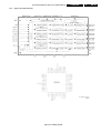
1
DVD-Video Player
DVD963SA
DVD963SA /001 /171 /691
CL 26532105_000.eps
280802
Contents
1
2
3
4
5
6
7
Page
Technical Specs and Connection Facilities
2
Safety Instructions, Warnings, and Notes
3
Directions for Use
4
Mechanical-, Dismantling Instructions, and Service
Hints
18
Diagnostic Software, Trouble Shooting and Test
Instructions
21
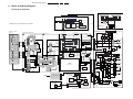
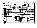
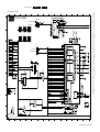
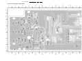
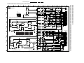
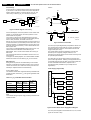
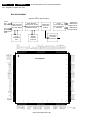
Block-, Wiring Diagram and Testpoint Overview
Block Diagram
41
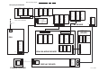
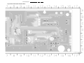
Wiring Diagram
42
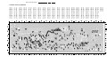
Testpoint Overviews
43
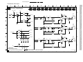
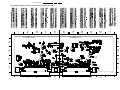
Electrical Diagrams and Print-Layouts
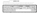
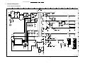
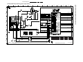
Diagram
Power Supply Unit
46
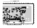
AV Board: SYS Clk & Control
(Diagram A1) 47
AV Board: Upsampling DAC
(Diagram A2) 48
AV Board: Audio DAC
(Diagram A3) 49
AV Board: Curr to Volt. Converter(Diagram A4) 50
AV Board: Audio
(Diagram A5) 51
AV Board: Video & SCART
(Diagram A6) 52
Front Board: Display
(Diagram D) 57
P-Scan Board: Line Doubler
(Diagram P1) 62
P-Scan Board: Encoder
(Diagram P2) 63
P-Scan Board: Video Output
(Diagram P3) 64
Standby Board
(Diagram S) 71
Double Scart Panel: Switching (Diagram S1) 72
Double Scart Panel: SCART
(Diagram S2) 73
Contents
Page
8
9
Alignments (Not Applicable)
Circuit Descriptions
List of Abbreviations
IC Data
10 Spare Parts List
77
77
86
87
91
PWB
53-56
53-56
53-56
53-56
53-56
53-56
58-61
65-70
65-70
65-70
71
74-76
74-76
©
Copyright 2002 Philips Consumer Electronics B.V. Eindhoven, The Netherlands.
All rights reserved. No part of this publication may be reproduced, stored in a
retrieval system or transmitted, in any form or by any means, electronic,
mechanical, photocopying, or otherwise without the prior permission of Philips.
Published by MW 0271 Service PaCE
Printed in the Netherlands
Subject to modification
EN 3122 785 12331
EN 2
1.
DVD963SA
Technical Specifications and Connection Facilities
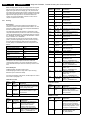
1. Technical Specifications and Connection Facilities
Specifications
PLAYBACK SYSTEM
DVD Video
SACD multi channel and SACD stereo
Video CD & SVCD
CD (CD-Recordable and CD-Rewritable)
MP3 CD
AUDIO PERFORMANCE (Without upsampling)
DA Converter
DVD
CD/Video CD
S-Video CD
24 bits
fs 96 kHz
fs 44.1 kHz
fs 48 kHz
fs 44.1 kHz
VIDEO PERFORMANCE
4 Hz - 44 kHz
4 Hz - 20 kHz
4 Hz - 22 kHz
4 Hz - 20 kHz
Signal-Noise (1kHz)
< -120 dB
Dynamic Range (1kHz)
< -95 dB
Crosstalk (1kHz)
< -110 dB
Total Harmonic Distortion (1kHz)
< -95 dB
MPEG MP3
MPEG Audio L3
RGB output
YUV output
CONNECTIONS
TV STANDARD (PAL/50Hz) (NTSC/60Hz)
Number of lines
Playback
S-Video output
Video output
Black Level Shift
Video Shift
625
525
Multistandard (PAL/NTSC)
0.7 Vpp into 75 ohm
Y: 1Vpp into 75 ohm
Pr/Cr Pb/Cb: 0.7Vpp into 75 ohm
Y: 1Vpp into 75 ohm
C: 0.3Vpp into 75 ohm
1 Vpp into 75 ohm
On/Off
Left/Right
AUDIO FORMAT
DSD
Multichannel and Stereo
MPEG/
Compressed Digital
Dolby Digital
16, 20, 24 bits
DTS/PCM
fs, 44.1, 48, 96 kHz
MP3
96, 112, 128, 256 kbps and
(ISO 9660)
variable bit rate fs 32, 44.1, 48kHz
Full decoding of Dolby Digital and DTS multi channel sound
Analogue Stereo Sound
Dolby Surround-compatible downmix from Dolby Digital
multi-channel sound
3D Sound for virtual 5.1 channel sound on 2 speakers
SCART
Y Pb/Cb Pr/Cr (480i/p)
S-Video Output
Video Output
Audio L+R output
Digital Output
2x Euroconnector
Cinch 3x (green, blue, red)
Mini DIN, 4 pins
Cinch (yellow) 2x
Cinch (white/red)
1 coaxial, 1 optical
IEC958 for CDDA / LPCM
IEC1937 for MPEG1/2, Dolby
Digital, DTS
6 channel analogue output
Audio Front L/R
Cinch (white/red)
Audio Surround L/R
Cinch (white/red)
Audio Centre
Cinch (blue)
Audio Subwoofer
Cinch (black)
CABINET
Dimensions (w x h x d) 435 x 101 x 315 mm
Weight
Approximately 4.6 Kg
POWER SUPPLY
SACD AUDIO PERFORMANCE
D/A Converter
SACD
Max. output voltage (0dB)
Channel unbalance
Cut-off frequency
DSD
fs 2.8224MHz DC - 100kHz
2V rms
<0.5 dB
50kHz (Front)
40kHz (Surround, Centre,
Subwoofer)
Signal-Noise (1kHz)
-125 dB
Dynamic Range (1kHz)
-105 dB
Crosstalk (1kHz)
-120 dB
Total Harmonic Distortion (1kHz)
-100 dB
Power inlet
Power usage
Power usage standby
110-240V, 50/60Hz
Approx. 30W
< 1W
* typical playing time for movie with 2 spoken languages and
3 subtitle languages
Specifications subject to change without prior notice
CL 26532105_050.pdf
280802
Safety Instructions, Warnings and Notes
DVD963SA
2.
EN 3
2. Safety Instructions, Warnings and Notes
2.1
Safety Instructions
2.2
Warnings
2.1.1
General Safety
2.2.1
General
Safety regulations require that during a repair:
• Connect the unit to the mains via an isolation transformer.
• Replace safety components, indicated by the symbol ,
only by components identical to the original ones. Any
other component substitution (other than original type) may
increase risk of fire or electrical shock hazard.
Safety regulations require that after a repair, you must return
the unit in its original condition. Pay, in particular, attention to
the following points:
• Route the wires/cables correctly, and fix them with the
mounted cable clamps.
• Check the insulation of the mains lead for external
damage.
• Check the electrical DC resistance between the mains plug
and the secondary side:
1. Unplug the mains cord, and connect a wire between
the two pins of the mains plug.
2. Set the mains switch to the 'on' position (keep the
mains cord unplugged!).
3. Measure the resistance value between the mains plug
and the front panel, controls, and chassis bottom.
4. Repair or correct unit when the resistance
measurement is less than 1 MΩ.
5. Verify this, before you return the unit to the customer/
user (ref. UL-standard no. 1492).
6. Switch the unit ‘off’, and remove the wire between the
two pins of the mains plug.
•
•
•
2.2.2
Laser
•
•
2.1.2
Laser Safety
•
This unit employs a laser. Only qualified service personnel may
remove the cover, or attempt to service this device (due to
possible eye injury).
Laser Device Unit
Type
Wavelength
Output Power
Beam divergence
: Semiconductor laser
GaAlAs
: 650 nm (DVD)
: 780 nm (VCD/CD)
: 20 mW (DVD+RW
writing)
: 0.8 mW (DVD
reading)
: 0.3 mW (VCD/CD
reading)
: 60 degree
All ICs and many other semiconductors are susceptible to
electrostatic discharges (ESD, symbol ). Careless
handling during repair can reduce life drastically. Make
sure that, during repair, you are at the same potential as
the mass of the set by a wristband with resistance. Keep
components and tools at this same potential. Available
ESD protection equipment:
– Complete kit ESD3 (small tablemat, wristband,
connection box, extension cable and earth cable) 4822
310 10671.
– Wristband tester 4822 344 13999.
Be careful during measurements in the live voltage section.
The primary side of the power supply (pos. 1005), including
the heatsink, carries live mains voltage when you connect
the player to the mains (even when the player is 'off'!). It is
possible to touch copper tracks and/or components in this
unshielded primary area, when you service the player.
Service personnel must take precautions to prevent
touching this area or components in this area. A 'lightning
stroke' and a stripe-marked printing on the printed wiring
board, indicate the primary side of the power supply.
Never replace modules, or components, while the unit is
‘on’.
•
The use of optical instruments with this product, will
increase eye hazard.
Only qualified service personnel may remove the cover or
attempt to service this device, due to possible eye injury.
Repair handling should take place as much as possible
with a disc loaded inside the player.
Text below is placed inside the unit, on the laser cover
shield:
CAUTION VISIBLE AND INVISIBLE LASER RADIATI ON WHEN OPEN AVO ID EXPOSURE TO BEAM
ADVARSEL SYNLIG OG USYNLIG LASERSTRÅLING VED ÅBNING UNDGÅ UDSÆTTELSE FOR STRÅLING
! ÅPNES UNNGÅ EKSPONERING FOR STRÅLEN
ADVARSEL SYNLIG OG USYNLIG LASERSTRÅLING NÅR DEKSEL
VARNING SYNLIG OCH OSYNLIG LASERSTRÅLNING NÄR DENNA DEL ÄR ÖPPNAD BETRAKTA EJ STRÅLEN
VARO! AVATT AESSA OLET ALTTIINA NÄKYVÄLLE JA NÄKYMÄTT ÖMÄLLE LASER SÄTEILYLLE. ÄLÄ KAT SO SÄT EESEEN
VORSICHT SICHTBARE UND UNSICHTBARE LASERSTRAHLUNG WENN ABDECKUNG GEÖFFNET NICHT DEM STRAHL AUSSETSEN
DANGER VISIBLE AND INVISIBLE LASER RADIATI ON WHEN OPEN AVO ID DIRECT EXPOSURE TO BEAM
AT TENTION RAYO NNEMENT LASER VISIBLE ET INVISIBLE EN CAS D'OUVERTURE EXPOSITION DANGEREUSE AU FAISCEAU
Figure 2-2 Warning text
2.2.3
Notes
Dolby
Manufactered under licence from Dolby Laboratories. “Dolby”,
“Pro Logic” and the double-D symbol are trademarks of Dolby
Laboratories. Confidential Unpublished Works. ©1992-1997
Dolby Laboratories, Inc. All rights reserved.
Figure 2-3
Figure 2-1 Class 1 Laser Product
Note: Use of controls or adjustments or performance of
procedure other than those specified herein, may result in
hazardous radiation exposure. Avoid direct exposure to beam.
Trusurround
TRUSURROUND, SRS and symbol (fig 2-4) are trademarks of
SRS Labs, Inc. TRUSURROUND technology is manufactured
under licence frm SRS labs, Inc.
Figure 2-4
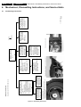
When a disc is loaded, unlock the tray by pushing the slide inwards with
a screwdriver and pull tray outwards.
Front Standby board
Î Remove cable connection.
Î Remove 2 screws 105.
(Board to Front cabinet)
Î Dismount board.
Manually opening of tray
When it is not possible to open the tray with the EJECT button,
the tray can be manually opened.
When no disc is loaded, unlock the tray by moving the slide from left
to right and pull tray outwards.
Front Display board 1002
Î Remove cable connections.
Î Remove 8 screws 100.
(Board to Front cabinet)
Î Dismount board.
P-scan board 1004
Î Removes flex connection.
Î Remove 2 screws 275
(skt cinch to back-plate) and
screw 261 (board to Pscan
bracket)
Î Dismount board
Remove 4 screws to remove loader.
A/V board 1001
Î Remove Double Scart board
(Only for DVD963SA /EU)
Î Remove flex and cable
connections.
Î Remove 4 screws 275
(skt cinch ,optical to backplate) and screw 280.
(S-video to back-plate)
Î Release 2 spacers locking.
Î Dismount board.
Double Scart board 1003
(Only for DVD963SA /EU)
Î Removes flex connection to
conn 1300 on scart board.
Î Remove 4 screws 290.
(scart to back-plate)
Î Dismount board.
Dismounting
Mounting
CL 26532105_002.eps
290802
Power supply unit 1010
Î Remove cable connections.
Î Remove 2 screws 190.
(Board to bottom frame)
Î Release spacer locking.
(Board to bottom frame)
Î Dismount board.
DVD963SA
DVD Monoboard
Î Remove flex and cable
connections from DVD
Loader to Monoboard.
Î Remove 4 screws 10 to 13.
(Monoboard to Loader,VAL6011/14)
Î Dismount Monoboard.
DVD Module 146
Î Removes flex connections
to A/V board.
Î Open tray (see instruction below).
Î Unlock Tray cover 025.
Î Remove 4 screws 185.
(Loader to bottom frame)
Î Close tray.
Î Lift module up slightly and move
backward to remove.
TopCover 300
Î Remove 7 screws 305.
Î Lift cover from rear side to
remove.
4.
Front cabinet 002
Î Remove cable connection.
Î Open Tray (see instruction below).
Î Unlock Tray cover 025 and
close tray.
Î Remove 2 screws 120
(Front cabinet to frame)
Î Unlock Front panel from frame by
releasing successively 6 snaps.
(2 on the side and 2 each on the top
and bottom)
Î Place Front panel in front of
the set ( service position ).
See exploded view of DVD963SA for item numbers
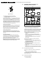
4.1
DISMANTLING INSTRUCTIONS
EN 18
Mechanical-, Dismantling Instructions, and Service Hints
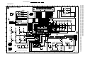
4. Mechanical-, Dismantling Instructions, and Service Hints
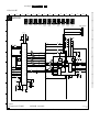
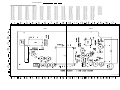
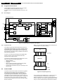
Dismantling Instructions
Figure 4-1 Dismantling Instructions
Mechanical-, Dismantling Instructions, and Service Hints
4.
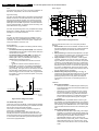
EN 19
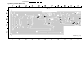
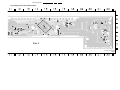
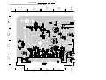
Exploded View
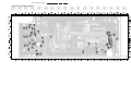
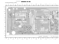
CL 26532105_003.eps
270802
4.2
DVD963SA
Figure 4-2 Exploded View
EN 20
4.
DVD963SA
4.3
Service Hints
4.3.1
Switched Mode Power Supply
Mechanical-, Dismantling Instructions, and Service Hints
4.3.3
For assistance with the repair process of the monoboard an
electronic fault finding guidance has been developed. This
program is called ComPair.
This ComPair program is available on CDROM.
The version of the CDROM for repair of the monoboard is V1.3
or higher and can be ordered with codenumber 4822 727
21637. This is an update CDROM, so when the ComPair
CDROM is used for the first time, one has to install the ComPair
Engine CDROM V1.2 first.
The V1.2 CDROM can be ordered with code number 4822 727
21634 and has to registered after instalation. The procedure for
registration is explained in the help file of the program and in
the CDROM booklet.
The cable to connect the monoboard with a PC can be ordered
with codenumber: 3122 785 90017.
All the hardware and software requirements of the systems,
necessary for working with ComPair, are described on the
CDROM.
The power supply unit has to be replaced in case of failure. The
schematic provided in the manual is only for information and no
service parts will be available.
4.3.2
DVD Module
This module can be repaired as follows:
1. The VAL6011/14 is a combination of loading mechanism
and DVD-mechanism. Both are not repairable units and in
case of failure, it has to be replaced with a new loader
VAL6011/14.
Note: When replacing with a new VAL6011/14, two solder
joints have to be removed after connecting the OPU flex foil
to the mono board.
The solder joints, which shortcircuits the laser diodes to
ground, are for protection against ESD. Refer to figures 25 and 2-6 for location of solder joints.
2. The mono board has to be repaired down to component
level. Repair handling of the monoboard requires a
workshop with sophisticated desoldering tools.
ComPair
4.3.4
Service Positions
Refer to dismantling instructions for dismounting of the board.
Figures 2-7 to 2-8 shows the service position that are
recommended during repair of the boards.
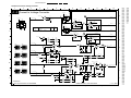
Figure 4-3 Solder joints
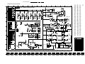
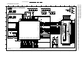
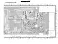
Figure 4-5 DVD963SA Layout
Figure 4-4 Solder joints
Figure 4-6 DVD963SA service manual
Diagnostic Software, Trouble Shooting and Test Instructions
DVD963SA
5.
EN 21
5. Diagnostic Software, Trouble Shooting and Test Instructions
5.1
Dealerscript
5.1.1
Purpose of Dealer Script
5.1.2
The dealer script can give a diagnosis on a standalone DVD
player, no other equipment is needed to perform a number of
hardware tests to check if the DVD player is faulty. The
diagnosis is simply a "error" or "pass" message. No indication
is given of faulty hardware modules. Only tests within the scope
of the diagnostic software will be executed hence only faults
within this scope can be detected.
Contents of Dealer Script
The dealer script executes all diagnostic nuclei that do not
need any user interaction and are meaningful on a standalone
DVD player.
The nuclei called in the dealer script are the following (the
number after each nucleus name corresponds with the number
being on the local display when the nucleus is executed during
the dealer script):
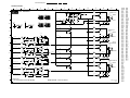
Nucleus
Display
Countdown
7
6
5
4
3
2
1
Nucleus
Nucleus
Number
Name
6
PapChksFl
12
13
11
15
16
63
Description
Calculate and verify checksum of FLASH memory
Checks the I2C interface with the slave processor on
the display board
PapI2cDisp
PapS2bEcho
Checks the I2C interface to the basic engine
PapI2cNvram
Checks the I2C interface with the NVRAM
PapNvramWrR
Pattern test of all locations in the NVRAM
CompSdramWrR
Pattern test of all locations in the SDRAM(s)
FURORERSdramWrRLow Pattern test of all locations in the SDRAM(s)
CL 26532053_052.eps
150502
Figure 5-1 Dealer script nuclei
Press 2 keys simultaneously
<OPEN/CLOSE> + <PLAY>
Connect to mains.
During the test, the following display
is shown: the counter counts down
from the number of nuclei to be run
before the test finishes. Example:
SET O.K.?
NO
YES
To exit DEALER SCRIPT, disconnect from mains
CL 26532053_053.eps
150502
Figure 5-2 Dealer Script
EN 22
5.
DVD963SA
5.2
Player Script
5.2.1
Purpose of Player Script
Diagnostic Software, Trouble Shooting and Test Instructions
Press the OPEN/CLOSE key to proceed to the next test.
5.2.4
The Player script will give the opportunity to perform a test that
will determine which of the DVD player's modules are faulty, to
read the error log and error bits and to perform an endurance
loop test. To successfully perform the tests, the DVD player
must be connected to a TV set to check the output of a number
of nuclei. For DVDv2b a multi-channel amplifier, a set of 6
speakers and an external video source are necessary to test.
To be able to check results of certain nuclei, the player script
expects some interaction of the user (i.e. to approve a test
picture or a test sound). Some nuclei (e.g. nuclei that test
functionality of the Basic Engine module) require that the DVD
player itself is opened, to enable the user to observe moving
parts and approve their movement visually. Only tests within
the scope of the diagnostic software will be executed hence
only faults within this scope can be detected.
Survey
Press 2 keys simultaneously
<OPEN/CLOSE> + <STOP>
Connect to mains
INTERACTIVE TESTS
DISPLAY PCB
DISPLAY TEST
DispDisplay (30a)
DispLed (29)
LED TEST
KEYBOARD TEST
5.2.2
Contents of Player Script
The player script contains all nuclei that are useful on a DVD
player that is connected to a TV set and help to determine
which module of the DVD player is faulty, as well as to read out
the contents of the error logs.
5.2.3
DispKeyb (27)
REMOTE CONTROL
DispRc (28)
P50 LOOP BACK TEST
DispP50 (60)
MONO PCB
DIGITAL PART
Structure of Player Script
The player script consists of a set of nuclei testing the three
hardware modules in the DVD player: the Display PWB, the
Digital PWB, and the Basic Engine.
Nuclei run by the player test need some user interaction. In the
next paragraph this interaction is described. The player test is
done in two phases:
1. Interactive tests: this part of the player test depends
strongly on user interaction and input to determine nucleus
results and to progress through the full test. Reading the
error log and error bits information can be useful to
determine any errors that occurred recently during normal
operation of the DVD player.
2. The loop test: this part of the player test will loop through
the list of nuclei indefinitely, till the player is reset. The list
of nuclei is as follows:
• PapChksFlash
• PapI2cNvram
• CompSdramWrR
• PapS2bEcho
• PapI2cDisp
At the beginning of the tests, the DSW version number will be
indicated on the local display of the DVD.
The display will look like the following:
CL 26532053_054.eps
150502
PICTURE TEST
VideoColDencOn (23a)
SOUND 1 TEST
SCART DVD TEST
AudioPinkNoiseOn (20a)
VideoScartSwDvd (55a)
SCART LOOP TEST
VideoScartSwPass (55b)
SOUND 2 TEST
AudioSineOn (21a)
MONO PCB(SERVO)
& BASIC ENGINE
VERSION NUMBER
TRAY TEST
BeTrayOut/In (43a/b)
SLEDGE TEST
BeSledgeOut/In (41a/b)
DISC MOTOR TEST
BeDiscMotorOn (39a/b)
FOCUS TEST
BeFocusOn (38a/b)
RADIAL TEST
BeRadialOn (40a/b)
JUMP TEST
BeGroovesIn/Mid/Out (42a/b/c)
TRAY TEST
BeTrayOut/In (43a/b)
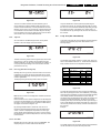
Figure 5-3
ERROR LOG & BITS
Pressing the PLAY key will proceed to the slave S/W version
display, which is shown on the local display of the DVD player.
The display will look like the following:
BeVer (37)
LOOP TEST
LogReadErr (31)
LogReadbits (32)
= Dealer script exclusive of test2
To exit player test,
disconnect from mains
CL 26532053_055.eps
150502
CL 16532162_030.eps
090102
Figure 5-4
Figure 5-5
Diagnostic Software, Trouble Shooting and Test Instructions
5.3
Display PCB
5.3.1
Display Test
KEY ID
0
1
2
3
4
5
6
7
E
F
The display test is performed by nucleus DispDisplay. By
putting a serie of test patterns on the local display, the local
display is tested. To step through all different patterns, the user
must either press OPEN/CLOSE (pattern is ok) or STOP
(pattern was incorrect) to proceed to the next pattern. The
display of patterns is continued in a cyclic manner, shown in
Fig. 5-6, until the user presses PLAY. If the user presses PLAY
before all display patterns are tested, the DispDisplay nucleus
will return FALSE (display test unsuccessful).
DVD963SA
5.
EN 23
KEY
PLAY
STOP
OPEN/CLOSE
STANDBY
NEXT
PREVIOUS
PAUSE
AUDIO DIRECT
SOUND MODE
REPEAT
CL 26532105_057.eps
300802
If OK, press OPEN/CLOSE
Figure 5-8
If NOK, press STOP
If OK, press OPEN/CLOSE
If NOK, press STOP
If OK, press OPEN/CLOSE
If NOK, press STOP
If any keys are detected more than once (due to hardware
error), the key-code is displayed twice (or more), with the
second digit increased by 1.
If the user does not press all keys minimally once (in any order),
the DispKeys nucleus will return FALSE and cause an error in
the overall result of the player script.
The user can leave the keyboard test by pressing the PLAY key
on the local display of the DVD player for at least one full
second.
The result of the keyboard test is shown on local display as
follows:
press PLAY to continue
CL 16532162_031.eps
080102
Figure 5-6
5.3.2
LED Test
CL 16532162_033.eps
080102
Figure 5-9
The LED(s) on the DVD player is (are) tested by nucleus
DispLed. The user must check if the LED(s) is (are) lighted; if it
is, press OPEN/CLOSE, if it is not, press STOP. By pressing
PLAY the script will proceed to the next test. If the user presses
PLAY before OPEN/CLOSE or STOP, the DispLed nucleus will
return TRUE (LED test successful).
5.3.3
Or
Keyboard Test
CL 16532162_034.eps
080102
The keyboard of the DVD player is tested by nucleus
DispKeyb. The user is expected to press all keys on the local
keyboard once. The code of the key pressed is shown on the
local display (1 hexadecimal digit) immediately followed by a
(hexadecimal) number indicating how many times that key has
been pressed. Example of the local display during this test:
Figure 5-10
Pressing PLAY on the local keyboard again will proceed to the
next text.
5.3.4
CL 196532162_032.eps
080102
Remote Control Test
The remote control of the DVD player is tested by nucleus
DispRc. The user must press any key on the remote control just
once. The codes of the key pressed will be shown on the local
display in hexadecimal format. Example:
Figure 5-7
The key-codes displayed on the local display will scroll from
right to left when the display gets full, the text "K" will remain
on display.
CL 16532162_035.eps
140102
Figure 5-11
In this example 23 is the hexidecimal code of the pressed RC
key. The user can leave the remote-control test by pressing
PLAY on the local keyboard of the DVD player. The remote
control test is successful if a code was received before the user
EN 24
5.
DVD963SA
Diagnostic Software, Trouble Shooting and Test Instructions
pressed the PLAY key. Pressing the PLAY key, before
pressing a key on the remote control, gives an error in the
remote control test (note that the remote control test will also
fail if a key on the remote control was pressed but no code was
received). The remote control test does not check upon the
contents of the received code, that is it will not be checked if the
received code matches the key pressed. If desired, the user
can manually check this code by using a code-table for the
remote control key-codes.
RC Key id
Hexadecimal code
STANDBY
0C
1
1
2
2
3
3
4
4
5
5
6
6
7
7
8
8
9
9
0
0
RETURN
83
DISPLAY
EF
DISC MENU
54
SYSTEM MENU
82
CURSOR UP
58
CURSOR DOWN
59
CURSOR LEFT
5A
CURSOR RIGHT
5B
OK
5C
PREVIOUS
21
NEXT
20
STOP
31
PLAY
2C
PAUSE
30
SUBTITLE
4B
ANGLE
85
ZOOM
F7
AUDIO
4E
REPEAT
1D
REPEAT A-B
3B
SHUFFLE
1C
SCAN
CL 96532065_013.eps
120799
Figure 5-13
Or
CL 96532065_014.eps
120799
Figure 5-14
Pressing PLAY on the local keyboard again will proceed to the
next test.
5.3.5
P50 Loop-Back Test
For the P50 loop-back test, the user must first press a key to
decide if the test is to be performed.
The display will show the following message:
CL 16532007_004.eps
090102
Figure 5-15
If the user presses STOP, the P50 test will be skipped.
If the user presses OPEN/CLOSE, the P50 test is performed
and the result is displayed as follows:
Test successful:
CL 16532007_005.eps
090102
Figure 5-16
Test fails:
CL 16532007_006.eps
090102
2A
CL 16532
162_037.eps
080102
Figure 5-17
Press the PLAY key to continue to the next text
Figure 5-12
After pressing PLAY, the result of the remote control test is
displayed on the local display of the DVD player as follows:
Diagnostic Software, Trouble Shooting and Test Instructions
5.4
Mono PCB Digital Part
5.4.1
Picture Test
DVD963SA
5.
EN 25
The test can be left by pressing the PLAY key for more than
one second.
5.4.3
The picture test is performed by putting a predefined picture
(colour bar) on the display (nucleus VideoColDencOn), and
asking the user for confirmation.
The display will show the following message:
Sound 2 Test
The second soundtest is performed by producing a sine sound
(nucleus AudioSineOn). The signal can be stopped by pressing
the STOP key.
The display will show the following message:
CL 96532065_015.eps
100102
CL 96532065_019.eps
100102
Figure 5-18
Figure 5-21
By pressing OPEN/CLOSE the user confirms the test, pressing
STOP will indicate the picture was invisible or incorrect.
Pressing PLAY will proceed to the next test. If the user presses
PLAY without pressing OPEN/CLOSE or STOP first, the result
of this test will be TRUE (picture ok).
Note: The colour bar must be simultaneously available on the
CVBS, YC, and RGB (or YUV) outputs available. On the
SCART only the CVBS and RGB signals will be available.
5.4.2
Sound 1 & SCART DVD Test
The first soundtest is performed by starting a pink noise sound
that needs confirmation from the user (nucleus
AudioPinkNoiseOn).
The display will show the following message:
CL 16532162_038.eps
080102
Figure 5-19
On the TV screen a colour bar (generated by nucleus
VideoColDencOn) is visible and the internally generated
pinknoise is audible.
By pressing the PLAY key, the user confirms the test. Pressing
the STOP key will indicate the sound was inaudible or
incorrect.
Note: Only for double scart models, SCART loop-through will
be simultaneously active during this test. SCART loop-through
will be measured with the aid of an external video source.
By pressing the PLAY key, there will be switched over to the
external source. This must become now visible on the TV
srcreen (using the SCART).
The local display will show the following message:
CL 16532162_039.eps
080102
Figure 5-20
The internally generated colour bar is still available on the
CVBS and Y/C outputs. And the pinknoise-signal is still
available on the cinch audio outputs. By pressing the OPEN/
CLOSE button, the internal generated colour bar becomes
visual again.
After the audio signal has been stopped, by pressing OPEN/
CLOSE, the user confirms the test. Pressing STOP will indicate
that something went wrong. Pressing PLAY will proceed to the
next. If the user presses PLAY without pressing OPEN/CLOSE
or STOP first, the result of this test will be TRUE (sound ok).
EN 26
5.
5.5
Basic Engine
5.5.1
Version Number
DVD963SA
Diagnostic Software, Trouble Shooting and Test Instructions
In the basic engine tests, the version number of the Basic
Engine will be shown first, as the following example:
CL 16532162_043.eps
080102
Figure 5-25
By pressing OPEN/CLOSE the user confirms that the disc
motor is running. Pressing STOP indicates the disc motor does
not work. Pressing PLAY proceeds to the next test, after a reset
of the disc motor (nucleus BeDiscMotorOff). If the user presses
PLAY before pressing OPEN/CLOSE or STOP, the result of
this test will be TRUE (disc motor is running).
CL 16532162_040.eps
080102
Figure 5-22
By pressing the PLAY key, the Basic Engine tests are started.
5.5.2
5.5.5
Tray Test
Focus Test (Visual Test)
The fourth Basic Engine test tests the focussing. First
focussing is turned on by calling nucleus BeFocusOn.
The display will look as follows:
First, the tray is tested. The purpose of this test is also to give
the user the opportunity to put a disc in the tray of the DVD
player. Some tests on the Basic Engine require that a disc (e.g.
DVD MPTD test disc) is present in the player. At the end of the
Basic Engine tests this tray test will be repeated solely to
enable the user to remove the disc in the tray.
The local display will look as follows:
CL 16532162_044.eps
080102
Figure 5-26
By pressing OPEN/CLOSE the user confirms that the
focussing was succesful. Pressing STOP indicates a focussing
failure. Pressing PLAY proceeds to the next test after a reset of
the focussing (nucleus BeFocusOff). If PLAY is pressed before
OPEN/CLOSE or STOP, the result of this test will be TRUE
(focus successful).
CL 16532162_041.eps
080102
Figure 5-23
By pressing OPEN/CLOSE the user can toggle the position of
the tray. Note that this test will not contribute to the test result
of the Basic Engine. Pressing PLAY will proceed to the next
test. At this point, the tray will be closed automatically by the
software if it was open.
5.5.3
5.5.6
The fifth Basic Engine test tests the radial functionality (nucleus
BeRadialOn).
The local display looks as follows:
Sledge Test (Visual Test)
The second Basic Engine test tests the sledge. The user can
move the sledge as many times as desired by using OPEN/
CLOSE (nucleus BeSledgeOut) and STOP (nucleus
BeSledgeIn). Pressing PLAY on the local keyboard proceeds
to the next test. Note that this test will not contribute to the test
result of the Basic Engine.
The local display will look as follows during the sledge test:
CL 16532162_045.eps
080102
Figure 5-27
By pressing OPEN/CLOSE the user confirms that the radial
function works.Pressing STOP indicates the function does not
work. Pressing PLAY proceeds to the next test, after a reset of
the radial (nucleus BeRadialOff). If the user presses PLAY
before pressing OPEN/CLOSE or STOP, the result of this test
will be TRUE (radial successful).
CL 165321625_042.eps
080102
Figure 5-24
5.5.4
Disc Motor Test (Visual Test)
The third Basic Engine test tests the disc motor (nucleus
BeDiscMotorOn).
The local display looks as follows:
Radial Test (Visual & Listening Test)
5.5.7
Jump Test (Listening Test)
The sixth and last Basic Engine test tests the jumping by calling
nuclei BeGroovesIn, BeGroovesMid and BeGroovesOut.
During this test, the local display looks as follows:
Diagnostic Software, Trouble Shooting and Test Instructions
DVD963SA
5.
CL 16532162_046.eps
080102
CL 16532162_048.eps
080102
Figure 5-31
Figure 5-28
Only the identification number (decimal) representing set
errorbits will be shown. By pressing OPEN/CLOSE or STOP,
the user can move forward or backward (respectively) through
the logged errorcodes. If the display only shows "EB-0", no
error bits were set. By pressing PLAY the user can continue to
the next test.
The user can switch between the three different types of
groove settings by pressing OPEN/CLOSE (forward to next
nucleus in the list In-Mid-Out), or STOP (backward in the list InMid-Out). This is done in a cyclic manner; note that this test will
not contribute to the test result of the Basic Engine. Pressing
PLAY proceeds to the next test, after the disc motor has been
shut off with a call to nucleus BeDiscMotorOff.
5.5.8
5.6
Tray Test
As a last action for the Basic Engine tests, the tray test is
repeated. The local display will look as follows:
Loop Test (See Table Below)
At the start of the loop test, the local display of the DVD player
will show the interactive player test result readout in the
following display:
CL 16532162_041.eps
080102
CL 16532162_049.eps
080102
Figure 5-29
Figure 5-32
This test is meant to give the user the opportunity to remove the
disc in the tray. The tray position can be toggled using the
OPEN/CLOSE key. The tray will be closed (by the software, if
it is open) before proceeding to the next test when the user
presses the PLAY key.
5.5.9
EN 27
The left side of the display contains a 3-digit code, which can
have a value between 000 and 111. These values indicate the
faulty modules and are to be interpreted as follows:
Displayed
Value
Error Log (See Table on Page 25)
Indication for each module
Basic Engine
Reading the error log and error bits information can be useful
to determine any errors that occurred recently during normal
operation of the DVD player. Reading the error log is done by
nucleus LogReadErr.
The display during the errorlog readout looks as follows :
000
001
010
011
100
101
110
111
ok
ok
ok
ok
faulty
faulty
faulty
faulty
Mono
PCB
ok
ok
faulty
faulty
ok
ok
faulty
faulty
Display
PCB
ok
faulty
ok
faulty
ok
faulty
ok
faulty
CL 96532065_031.eps
120799
Figure 5-33
CL 16532162_047.eps
080102
Figure 5-30
Note: Previous versions of the diagnostic software showed a 8digit error code.
Due to limitations in the number of digits that can be displayed
by some front panel displays, the most significant digits will not
be shown. This can be done since all the error codes used by
this player has set these 2 digits to “00”
By pressing OPEN/CLOSE or STOP the user can move
forward or backward (respectively) through the logged error
codes. If "0000" is displayed at all positions, the error log is
empty. Display of the logged errors is done in a cyclic manner.
By pressing PLAY on the local keyboard, the user can proceed
to the next test.
The loop test will perform the same nuclei as the dealer test,
but it will loop through the list of nuclei indefinitely. The display
of the DVD player will display not only the three digits indicating
correct/faulty modules and the last found error code (as
mentioned, faults are detected as far as they can be within the
scope of the diagnostic software), but also a loop counter
indicating how many times the loop has been gone through. If
an error was detected, the display will remain as in figure 5-34
until the user presses the PLAY key and then it will continue to
the next loop.
Example:
CL 16532162_050.eps
080102
5.5.10 Error Bits
Figure 5-34
Reading the error bits is done by nucleus LogReadBits. The
display during the errorbits readout looks as follows:
The 2-digit number (23) on the right of figure 5-32 indicates the
number of times the loop test has been performed.
EN 28
5.
DVD963SA
Diagnostic Software, Trouble Shooting and Test Instructions
After one loop cycle: Display the 3-digit module bits together
with the last error code which occured in the loop test. The 4
digits at the right side of the display (fig. 5-34) show the last
error that was found during the loop test. The leftmost two digits
(54) of this code indicates which nucleus resulted in a fault. The
rightmost two digits (03) refer to the faultcode within that
nucleus. For further explanation of this error code, refer to
chapter 5.8 (Nuclei Error Codes).
5.6.1
Error
Number Error name
S2B_SLEDGE Sledge could not be moved to
home position.
0104
S2B_FOCUS
0105
S2B_MOTOR Motor could not reach speed
within timeout
0106
S2B_RADIAL
0107
S2B_PLL_LO PLL could not lock in Accessing
CK
or Tracking state
0108
SBC_HEADE
R_TO
0109
S2B_SBC_NO Requested subcode item could
T_FOUND
not be found.
010A
S2B_TRAY
010B
S2B_TOC_RE TOC could not be read within
AD
timeout period.
010C
S2B_JUMP
010D
S2B_NON_EX Attempt to access a non-existing
IST_SES
session.
010E
S2B_NON_EX Caller tries to acces a nonIST_BCA
existing BCA area
010F
Speed setting A wrong or inappropraiate speed
value has been set
Errorlog
Explanation:
The application errors will be logged in the NVRAM. The
maximum number of error bytes that will be visible is 16. The
first word (4 digits) of the byte is the component identification,
the last word is the error code.
The diagnostics software will present a combination of this
component identification plus an error code on the local display
(and on the attached terminal). The last reported error is shown
as < 00000000, the oldest visible error as 00000000 > and the
errors in between as < 00000000 >.
The devices that may report errors are the serial controller
(UART), the basic engine (BE), the slave processor (SLPH),
the SACD Stream Manager (SSM) and the SACD Media
Access (SMA). The identification of these components is as
follows:
Component name
Component identification
Serial controller (UART)
000A
Engine (BE)
0016
Slave Processor (SLPH)
001A
SACD Stream Manager
(SSM)
001C
SACD Media Access (SMA)
002E
Diagnostic software (DS)
Dxxx
The tables in the next chapters list the error code and
corresponding problem. The column ‘Explanation’ holds a
more elaborate description and the most likely reason for the
error.
Some Examples:
002E0000 (SMA reported a timeout error)
0016010A (Engine could not fully close or open the tray)
D0010001 (Flash checksum failed).
For further explanation of DS errors, see description of nucleui
error codes in paragraph 5.8.
0000
Explanation
BUF_OVE To many characters were offered in
RFLOW
too little time. Reason: system was
too busy doing other jobs.
0001
COMMUNI Usually a protocol error. Reason:
CATION
bad connection between engine
and processor.
0002
TIME OUT
Focus failure
Servo didn't get on track after
several retries.
Header timeout
Tray could not be opened or
closed completely.
Requested seek could not be
performed.
0116
NO_DISC
No disc selected
011A
TRAY_INIT
After reset, initialized tray
011B
NO TOC INFO No TOC information in lead-in
area or erase TOC found
01F0
S2B_OVERR
UN
01F1
S2B_COMM_ Not enough bytes are received
TO
over S2B Reason: see
S2B_ILL_COMMAND error
01F2
S2B_PARITY
01F3
S2B_ILL_PHA CMD IDC is not valid,
SE
transmission out of sync.
Reason: see
S2B_ILL_COMMAND error
01F4
S2B_ILL_NR_ Byte count has an illegal value.
OF_BYTES
Reason: see
S2B_ILL_COMMAND error
UART Error Codes
Error
Error
Number name
Explanation
0103
Too many bytes received over
S2B Reason: see
S2B_ILL_COMMAND error
Byte received with parity error.
Reason: see
S2B_ILL_COMMAND error
SLPH Error Codes
Error
Number Error name
0000
Explanation
COMMUNICA Error in I2C communication.
TION
Reason: bad connection
between slave processor and
main processor.
SSM Error Codes
BE Errors
Error
Number Error name
Error
Code
Explanation
0101
S2B_ILL_CO
MMAND
0102
S2B_ILL_PAR Command not allowed in this
AM
state or unknown. Reason: see
S2B_ILL_COMMAND error
Error name
Explanation
0006
SP_SYNCER
ROR
System cannot get synchronised
with sectors coming from disc.
Reason: Usually a damaged
disc or the player was dropped/
pushed during operation. If not,
the engine is malfunctioning.
0007
SP_EDCERR Data coming from disc is
OR
damaged. Reason: see
SP_SYNCERROR
Parameter(s) not valid for this
command. Reason: some
communication problem
between UART and engine.
Diagnostic Software, Trouble Shooting and Test Instructions
Error
Code
0008
5.6.2
DVD963SA
5.
EN 29
SMA Error Codes
Error name
Explanation
SP_CONTINU Sequence of sectors coming
ITYERROR
from disc is incorrect. Reason:
see SP_SYNCERROR
0009
DMX_CONTI
NUITYERRO
R
Sequence of sectors is incorrect.
Reason: problem with buffer
RAM
000A
LLD_ERROR
An illegal audio format was
offered to the decoder. Reason:
unknown audio type on disc or
problem with buffer RAM
000B
BCU_ERROR Internal problem in Furore chip
Error
Number Error name
0000
SMA_TIMEO
UTERROR
Explanation
Data coming from disc not in
time. Reason: damaged disc or
engine problem.
Reprogramming of New Mono Boards.
Caution
This information is confidential and may not be distributed. Only a qualified service person should
reprogram the mono board.
After reset of NV-memory or repair of the mono board, all the customer settings and also the region code
will be lost.
Reprogramming of the mono board will put the player back in the state in which it has left the factory,
i.e. with the default settings and the allowed region code.
Reprogramming is limited to 25 times
When the counter reaches 25, reprogramming is not possible anymore
Reprogramming will be done by way of the remote control.
Put the player in stop mode, no disc loaded.
Press the following keys on the remote control:
<PLAY> followed by numerical keys <1> <5> <9>
The display shows: “- - - - - - - - - - -”
Press now successively the following keys :
for DVD963SA /001
for DVD963SA 171
for DVD963SA 691
: <2><2><2> <0><1><2><0><0>
: <1><1><1> <0><1><0><0><0>
: <3><2><3> <0><1><0><0><0>
Press <PLAY> again.
The TV screen will become BLUE during a short time to confirm that the mono board has been
reprogrammed.
CL 26532105_053.eps
280802
Figure 5-35 Reprogamming code
EN 30
5.6.3
5.
DVD963SA
Diagnostic Software, Trouble Shooting and Test Instructions
Trade Mode
When the player is in Trade Mode, the player cannot be
controlled by means of the front key buttons, but only by means
of the remote control.
TO ACTIVATE TRADE MODE
TO DEACTIVATE TRADE MODE
POWER ON
POWER ON
DURING STOP MODE AND W/O DISC.
PRESS REMOTE KEYS COMBINATION
<PLAY> <259> <PLAY>
DURING STOP MODE AND W/O DISC.
PRESS REMOTE KEYS COMBINATION
<PLAY> <259> <PLAY>
PLAYER IS IN TRADE MODE WHEN
PRESSING FRONT KEYS,
THE PLAYER DOESN'T RESPOND
PLAYER IS IN NORMAL MODE WHEN
PRESSING FRONT KEYS,
THE PLAYER WILL RESPOND
CL16532162_052.eps
0850102
Figure 5-36
Note: To activate and deactivate the Trade Mode with the disc
in the player, the procedure is similar to above, except that the
remote control keys combination is pressed at the instant when
the local display is flashing “READING”
5.7
Menu and Command Mode Interface
5.7.1
Layout of Results Diagnostic Nuclei
Results returned from a Diagnostic Nucleus will be displayed in
the following layout:
< number >< string > [ok | ER]
< number >: is a 4-digit decimal number padded with leading
zeros if its value is less than 4 digits. The first 2 digits identify
the generating nucleus (or group of nuclei) while the latter 2
digits indicate the error number.
< string >: is a text string containing information about the result
of the Diagnostic Nucleus.
< number > and < string > are defined in [SSD_DN] in the
output sections of each Nucleus.
Examples:
1. 0001Unknown command ER @
2. 3100OK @
3. 0901Data line X is not connected to the DRAM ER@
Activation
Switch the player on and the following text will appear on the
screen of the terminal (program):
DVDv4 Diagnostic Software version 5.03
(M)enu, (C)ommand or (S)2B interface ? [M]:@ C <enter>
SDRAM Interconnection test passed
Basic SDRAM test passed
Slave Processor: SLAVE2
DD:>
CL 26532105_058.eps
020902
Figure 5-37
The first line indicates that the Diagnostic software has been
activated and contains the version number. The second line
lets the user choose the interface format. Enter ‘C’ to select
Command Mode and the next three lines are the successful
result of the two subsequent basic tests (nuclei 2, ,4 and the
detection of the display type used by the panel respectively). If
not all these messages appear on the terminal screen, then the
related nucleus found an error. The last line is the prompt
("DD>"). The diagnostic software is now ready to receive
commands.
Command Overview of Nuclei
The following table gives an overview of all available nuclei.
The first column contains an identification number, the second
contains the name of a nucleus and the last column indicate the
description of the nucleus.
Note: User confirmation is necessary during front panel tests
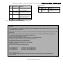
Table 5-1 Basic diagnostic nuclei
5.7.2
Command Mode Interface
Set-up Physical Interface Components
Hardware required:
• Service PC
• one free COM port on the Service PC
• special cable to connect DVD player to Service PC
The service PC must have a terminal emulation program (e.g.
OS2 WarpTerminal or Procomm) installed and must have a
free COM port (e.g. COM1). Activate the terminal emulation
program and check that the port settings for the free COM port
are: 19200 bps, 8 data bits, no parity, 1 stop bit and no flow
control. The free COM port must be connected via a special
cable to the RS232 port of the DVD player. This special cable
will also connect the test pin, which is available on the
connector, to ground (i.e. activate test pin).
Code number of PC interface cable: 3122 785 90017
Ref. # Reference Name
Remark
1
BasicSpAcc
Serial port Access test/
initialization
2a
BasicInterconDram
Data and address bus
Interconnection (only for
development)
2b
BasicInterconSdram Data and address bus
interconnection
3
BasicDramWrR
DRAM Write Read (only for
development)
4
BasicSdramWrR
SDRAM Write Read
Diagnostic Software, Trouble Shooting and Test Instructions
Table 5-2 Processor and peripherals
DVD963SA
5.
EN 31
Ref. # Reference Name
Remark
80d
DAC_ModeDSD
Sets DAC to DSD mode
81a
DAC_LowPowerStandby Enable Low Power
On
Standby
Ref. # Reference Name
Remark
6
PapChksFl
Checksum FLASH
7a
PapUclkAclkCdda
uClock A_CLK in CD-DA
mode
81b
DAC_LowPowerStandby Disable Low Power
Off
Standby
7b
PapUclkAclkDvd
uClock A_CLK in DVD mode
82a
7c
PapUclkAclkDvd96
uClock A_CLK in DVD
(96kHz) mode
DAC_UpsamplingFreq19 Sets Upsampling
2k
frequency to 192kHz
82b
10
PapFlashWrAcc
FLASH Write Access (only for
development)
DAC_UpsamplingFreq96 Sets Upsampling
k
frequency to 96kHz
82c
DAC_UpsamplingOn
Enable upsampling
11
PapI2cNvram
I2C NVRAM access
82d
DAC_UpsamplingOff
Disable upsampling
12
PapI2cDisp
I2C Display PWB
13
PapS2bEcho
S2B Echo
14
PapS2bPass
S2B Pass-through
15
PapNvramWrR
NVRAM Write Read
Ref. # Reference Name
Remark
62
PapChksSum
Show checksums stored in
flash
17a
VidPortOutAA
Output the value 0XAA at
the Digital Video Interfac
e Port
17b
VidPortOut55
Output the value 0X55 at
the Digital Video Interfac
e Port
23a
VideoColDencOnPAL
Colourbar (PAL) DENC
On
23b
VideoColDencOff
Colourbar DENC Off
23c
VideoColDencOnNTSC
Colourbar (NTSC) DENC
On
24a
VideoProgMPEGon
Progressive DigitalVideo Colour Bar
ON
24b
VideoYuvMPEGon
Enhanced YUVDigitalVideo Colour Bar
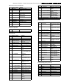
Table 5-3 Components
Ref. # Reference Name
Remark
16
SDRAM Write Read
CompSdramWrR
Table 5-4 Audio
Ref. # Reference Name
Remark
19a
AudioMuteOn
Audio Mute On
19b
AudioMuteOff
Audio Mute Off
20a
AudioPinkNoiseOn
Audio Pinknoise On
20b
AudioPinkNoiseOff
Audio Pinknoise (or beep
tone) Off
20c
AudioBeepToneOn
Audio Beep Tone On
21a
AudioSineOn
Audio Sine signal On/Off
21b
AudioSineBurst
Audio Sine signal Burst
56a
AudioLfePortHigh
Set the LFE_SEL port to
HIGH
56b
AudioLfePortLow
Set the LFE_SEL port to
LOW
66a
DAC_I2C
Resets DAC and check
I2C communication with
DAC
66b
DAC_I2CEnable
Enable I2C
communication to AV
board
Table 5-5 Video
25a
VideoScartLo
Scart Low
25b
VideoScartMi
Scart Medium
25c
VideoScartHi
Scart High
54
VideoScartSwComm
Scart Switch
communication
55a
VideoScartSwDvd
Scart Switch Dvd
55b
VideoScartSwPass
Scart Switch Passthrough
57a
VideoScartPinLo
PIO-pins as used in 2A
for Scart-switching
57b
VideoScartPinMi
PIO-pins as used in 2A
for Scart-switching
57c
VideoScartPinHi
PIO-pins as used in 2A
for Scart-switching
61a
VideoColOutRGB
(ST5508)
Output RGB from
ST5508
61b
VideoColOutYUV
(ST5508)
Output YUV from
ST5508
66c
DAC_I2CDisable
Disable I2C
communication to AV
board
67a
DAC_ClockInternal
Uses internal clock from
monoboard for DAC
(256fs)
67b
DAC_ClockExternal
Uses external clock for
DAC (384fs)
Ref. # Reference Name
Remark
68a
DAC_AudioPreMuteOn
Enable Audio Pre-mute
pin
26
Version number
68b
DAC_AudioPreMuteOff
Disable Audio Pre-mute
pin
27
DispKeyb
Keyboard
28
DispRc
Remote Control
69a
DAC_CenterOn
Enable Center on pin
29
DispLed
LEDs
Disable Center on pin
30a
DispDisplay
VFT Display test
DispLCDisplay
LCD Display test
69b
DAC_CenterOff
Table 5-6 Display (slave processor)
DispVer
79
DAC_Reset
Resets DAC
30b
80a
DAC_ModeCDDA
Sets DAC to CDDA
mode
30c
DispLCDBkLight
LCD Backlight test
60
DispP50
P50 loopback test
80b
DAC_ModeDVD48
Sets DAC to DVD mode
(48kHz)
80c
DAC_ModeDVD96
Sets DAC to DVD mode
(96kHz)
EN 32
5.
DVD963SA
Diagnostic Software, Trouble Shooting and Test Instructions
Table 5-7 Log (Error logging in Nvram)
Ref. # Reference Name
Remark
31
LogReadErr
Read last Errors
32
LogReadBits
Read errors Bits
33
LogReset
Reset
Ref. # Reference Name
Remark
84a
Furore_High
Sets Furore output pins
DSD_PCM0-9 to high
84b
Furore_Low
Sets Furore output pins
DSD_PCM0-9 to low
Table 5-11 Karaoke (not available)
Table 5-8 Miscellaneous
Ref. # Reference Name
Ref. # Reference Name
Remark
34
MiscReadConfig
Read Configuration area
from NVRAM
35
MiscNvramReset
NVRAM Reset
36
MiscNvramMod
Modify NVRAM contents
46
MiscApplVer
Read version of
application software
47a
MiscTrayOpenNr
Read the number of
times the tray opened
47b
MiscPowerOnTime
Read the total time the
player's power has been
on
47c
MiscPlayTimeCddaVcd
Read the Playtime of
CDDA and VCD discs
47d
MiscPlayTimeDvd
Read the Playtime of
DVD discs
Table 5-9 Basic engine
5.7.3
Remark
48a
KaraokeModeOff
Switch Karaoke mode off
48b
KaraokeModeOn
Switch Karaoke mode on
49
KaraokeMicInput
Check path from the
microphone input to audio
output
50a
KaraokeKeyOn
Set Karaoke Key to the
maximum level (1200 cent)
50b
KaraokeKeyOff
Set Karaoke Key to flat octave
(0 cent)
51a
KaraokeEchoOn
Set Echo Control fuction on
51b
KaraokeEchoOff
Set Echo Control function off
Menu Mode Interface
Activation
Switch the player on and the following text will appear on the
screen of the terminal (program):
DVDv4 Diagnostic Software version 5.03
Ref. # Reference Name
Remark
37
BeVer
Version number
38a
BeFocusOn
Focus On
38b
BeFocusOff
Focus Off
39a
BeDiscmotorOn
Discmotor On
39b
BeDiscmotorOff
Discmotor Off
Press ENTER to go to main menu
40a
BeRadialOn
Radial control On
CC: > <enter>
(M)enu, (C)ommand or (S)2B interface ? [M]:@ <enter>
SDRAM Interconnection test passed
Basic SDRAM test passed
Slave Processor: SLAVE2
40b
BeRadialOff
Radial control Off
MAIN MENU
41a
BeSledgeIn
Sledge Inwards
41b
BeSledgeOut
Sledge Outwards
42a
BeGroovesIn
jump Grooves to Inside
42b
BeGroovesMid
jump Grooves to Middle
42c
BeGroovesOut
jump Grooves to Outside
43a
BeTrayIn
Tray In
1.
2.
3.
4.
5.
6.
7.
8.
43b
BeTrayOut
Tray Out
44
BeReset
Reset Basic Engine
58a
LaserCdOn
CD Laser on
58b
LaserCdOff
CD Laser off
58c
LaserDvdOn
DVD Laser on
58d
LaserDvdOff
DVD Laser off
70
BedReadFlashID
Read flash memory
manufacturer and device ID
71
BedCalcRomChks Calculate ROM checksum
um
72
BedScratchTest
Test scratch detection circuit
Table 5-10 Furore IC
Ref. # Reference Name
Remark
Audio ...
Video ...
Front Panel ...
Basic Engine ...
Processor Peripherals ...
Error Log ...
Furore ...
Miscellaneous ...
Select >
CL 26532105_059.eps
020902
Figure 5-38 Screen menu
The first line indicates that the Diagnostic software has been
activated and contains the version number. The next lines are
the successful result of the SDRAM interconnection test and
the basic SDRAM test. The last line allows the user to choose
between the four possible interface forms. If pressing M has
made a choice for Menu Interface, the Main Menu will appear.
Layout of Menu and Submenu
The following menu layout will appear after starting up the DVD
player in menu mode. The symbol “- - -”” indicates that the
current menu choice will invoke the display of a submenu. The
number between [ ] idicates the nucleus number. These
numbers will not be shown on the screen.
63
Furore_SdramWrR Furore SDRAM Write Read
test
64
Furore_SdramWrR Furore SDRAM
Fast
interconnection test
Menus
65
Furore_Id
Furore version ID check
83
Furore_Reset
Furore reset
MAIN MENU
1
Audio...
2
Video...
3
Front Panel...
Diagnostic Software, Trouble Shooting and Test Instructions
4
5
6
7
8
DVD963SA
5.
EN 33
MAIN > AUDIO > SINE WAVE MENU
1
Audio Sine On
[21a]
2
Audio Burst On
[21b]
Basic Engine...
Processor Peripherals...
Error Log...
Furore...
Miscellaneous...
MAIN > AUDIO > DIGITAL PORTS MENU
1
No tets available
First Level Submenus
MAIN > AUDIO > EXT DAC BOARD MENU
1.
DAC Reset
[79]
2.
I2C Test...
3.
Clock...
4.
Audio...
5.
Low Power Standby...
6.
DAC Mode...
MAIN > AUDIO MENU
1
Mute...
2
Pink Noise...
3
Sine Wave...
4
Digital Ports...
5
Ext. DAC Board...
MAIN > VIDEO MENU
1
Colourbar...
2
Scart...
3
Digital Port...
MAIN > FRONT PANEL MENU
1
Slave Processor...
2
VFT Display
3
LCD Display
4
LCD BkLight
5
Keyboard
6
LEDs
7
Remote Control
8
P50 Check
[30a]
[30b]
[30c]
[27]
[29]
[28]
[60]
MAIN > BASIC ENGINE MENU
1
Reset
[44]
2
Version
[37]
3
S2B...
4
Loader Mechanism...
5
Special Diagnostics...
[31]
[32]
[33]
MAIN > FURORE MENU
1
SDRAM Write/Read
2
SDRAM Write/Read
3
Chip Revision ID
4
Set DSD_PCM Output High
5
Set DSD_PCM Output Low
6
Reset Furore IC
[63]
[64]
[65]
[84a]
[84b]
[83]
MAIN > MISCELLANEOUS MENU
1
Statistics Info...
2
Read DVD Application version[46]
[54]
[55a]
[55b]
[25a]
[25b]
[25c]
MAIN > FRONT PANEL > SLAVE PROCESSOR MENU
1
Bus Comms Check
[12]
2
S/W Version
[26]
MAIN > BASIC ENGINE > S2B MENU
1
S2B Echo
[13]
2
S2B Pass-Through
[14]
MAIN > BASIC ENGINE > MECHANISM MENU
1
Disc Motor...
2
Laser...
3
Tray...
4
Focus...
5
Radial...
6
Sledge...
7
Grooves...
MAIN > BASIC ENGINE > SPECIAL DIAGNOSTICS MENU
1
Read FlashID
[70]
2
ROM Checksum
[71]
3
Scratch Circuit
[72]
MAIN > PROCESSOR PERIPHERALS > PCM CLOCK MENU
1
Ext PCM_CLK In CDDA Mode (11.3MHz)
[7a]
2
Ext PCM_CLK In DVD Mode (12.3MHz)
[7b]
3
Ext PCM_CLK In DVD96kHz Mode (24.6MHz) [7c]
Second Level Submenus
MAIN > AUDIO > MUTE MENU
1
Mute On
2
Mute Off
3
Mute Front LR On (963 only)
4
Mute Front LR Off (963 only)
MAIN > VIDEO > SCART MENU
1
I2C Scart IC Check
2
Scart To DVD
3
Scart Pass Through
4
Scart Pin 8 Low (0 to 2)V
5
Scart Pin 8 Mid (4.5 to 7)V
6
Scart Pin 8 Hi(9.5 to 12)V
MAIN > VIDEO > DIGITAL PORT MENU
1
Video Port Out 0xAA
[17a]
2
Video Port Out 0x55
[17b]
3
P-scan board IO exp
[17c]
MAIN > PROCESSOR PERIPHERALS MENU
1
Clock...
2
Flash...
3
NVRAM...
4
SDRAM Write/Read
[16]
MAIN > ERROR LOG MENU
1
Read Last Errors
2
Read Error Bits
3
Reset Error Log
MAIN > VIDEO > COLOURBAR MENU
1
Colourbar DENC On (PAL)
[23a]
2
Colourbar DENC On (NTSC) [23c]
3
Colourbar DENC/MPEG Off
[23b]
4
ProgressiveScan MPEG On
[24a]
5
Enhanced YUV MPEG On
[24b]
6
Set Video Out To RGB
[61a]
7
Set Video Out To YUV
[61b]
[19a]
[19b]
[19c]
[19d]
MAIN > AUDIO > PINK NOISE MENU
1
Pink Noise On
[20a]
2
Pink Noise / Beep Tone Off [20b]
3
Beep Tone On
[20c]
MAIN > PROCESSOR PERIPHERALS > FLASH MENU
1
Verify FLASH Checksum [6]
2
Show FLASH Checksum
[62]
MAIN > PROCESSOR PERIPHERALS > NVRAM MENU
1
I2C NVRAM Acces
[11]
2
NVRAM Config
[34]
3
NVRAM Reset
[35]
EN 34
4
5
5.
DVD963SA
NVRAM Modify
NVRAM Read/Wr Test
Diagnostic Software, Trouble Shooting and Test Instructions
3
[36]
[15]
MAIN > MISCELLANEOUS > STATISTICS INFO MENU
1
Total Nr Of Times Tray Open
[47a]
2
Total Time Power On
[47b]
3
Total Play-Time CDDA & VCD
[47c]
4
Total Play-Time DVD
[47d]
5.8
Jump To Outside Grooves [42c]
Nuclei Error Codes
In the following tables the error description of the error codes
will be described.
5.8.1
Audio Nuclei
Third Level Submenus
MAIN > AUDIO > EXT DAC BOARD > I2C TEST MENU
1.
I2C Test
[66a]
2.
I2C Enable Pin On
[66b]
3.
I2C Enable Pin Off
[66c]
MAIN > AUDIO > EXT DAC BOARD > CLOCK MENU
1.
Clock Internal
[67a]
2.
Clock External
[67b]
3.
Clock Upsampling 192k (963 only)
[82a]
4.
Clock Upsampling 96k (963 only)
[82b]
5.
Clock Upsampling On (963 only)
[82c]
6.
Clock Upsampling Off (963 only)
[82d]
Error
code
Error text
1800
Audio Deemp On OK
1820
Audio Deemp Off OK
1880
Audio Deemp Tri OK
1900
Audio mute On OK
1920
Audio mute Off OK
1940
Audio Front LR mute On OK
1960
Audio Front LR mute Off OK
2000
Audio Pinknosie On OK
2001
Audio Pinknoise On DAC fail
2020
Audio Pinknoise Off OK
MAIN > AUDIO > EXT DAC BOARD > AUDIO
1.
Audio Pre-Mute On
[68a]
2.
Audio Pre-Mute Off
[68b]
3.
Audio Center On
[69a]
4.
Audio Center Off
[69b]
2040
Audio Beep tone On OK
2041
Audio Beep tone On DAC fail
MAIN > AUDIO > EXT DAC BOARD > LOW POWER
STANDBY
1.
Low Power Standby On
[81a]
2.
Low Power Standby Off
[81b]
2121
Audio Sine Burst DAC fail
6600
DAC I2C OK
6601
DAC I2C Bus busy
6602
DAC I2C expander
6603
DAC I2C DAC 4362
6620
DAC I2C enable OK
6640
DAC I2C disable OK
MAIN > AUDIO > EXT DAC BOARD > DAC MODE MENU
1.
DAC CDDA Mode
[80a]
2.
DAC DVD48 Mode
[80b]
3.
DAC DVD96 Mode
[80c]
4.
DAC DSD Mode
[80d
MAIN > BASIC ENGINE > MECHANISM > DISC MOTOR
MENU
1
Disc Motor On
[39a]
2
Disc Motor Off
[39b]
2100
Audio Sine On OK
2101
Audio Sine On DAC fail
2120
Audio Sine Burst OK
6700
DAC Clk internal OK
6701
DAC Clk internal I2C bus busy
6702
DAC Clk internal I2C failed
6720
DAC Clk external OK
6721
DAC Clk external I2Cbus busy
6722
DAC Clk external I2C failed
6800
DAC Audio pre-mute On OK
MAIN > BASIC ENGINE > MECHANISM > LASER MENU
1
CD Laser On
[58a]
2
CD Laser Off
[58b]
3
DVD Laser On
[58c]
4
DVD Laser Off
[58d]
6801
DAC Audio pre-mute On I2C bus busy
6802
DAC Audio pre-mute On I2C failed
MAIN > BASIC ENGINE > MECHANISM > TRAY MENU
1
Tray Open
[43b]
2
Tray Close
[43a]
6900
DAC Center On OK
6901
DAC Center On I2C bus busy
6902
DAC Center On I2C failed
6820
DAC Audio pre-mute Off OK
6821
DAC Audio pre-mute Off I2C bus busy
6822
DAC Audio pre-mute Off I2C failed
6920
DAC Center Off OK
MAIN > BASIC ENGINE > MECHANISM > FOCUS MENU
1
Focus On
[38a] (load DVD first)
2
Focus Off
[38b]
6921
DAC Center Off I2C bus busy
6922
DAC Center Off I2C failed
7900
DAC Reset OK
MAIN > BASIC ENGINE > MECHANISM > RADIAL MENU
1
Radial Control On
[40a] (load DVD first)
2
Radial Control Off
[40b]
7901
DAC Reset I2C bus busy
7902
DAC Reset I2C expander
8000
DAC Mode CDDA OK
8001
DAC Mode CDDA I2C bus busy
MAIN > BASIC ENGINE > MECHANISM > SLEDGE MENU
1
Sledge Inwards
[41a]
2
Sledge Outwards
[41b]
8002
DAC Mode CDDA I2C failed
MAIN > BASIC ENGINE > MECHANISM > GROOVES (Uses
DVD) MENU
1
Jump To Inside Grooves [42a]
2
Jump To Middle Grooves [42b]
8020
DAC Mode DVD48 OK
8021
DAC Mode DVD48 I2C bus busy
8022
DAC Mode DVD48 I2C failed
8040
DAC Mode DVD96 OK
8041
DAC Mode DVD96 I2C bus busy
8042
DAC Mode DVD96 I2C failed
Diagnostic Software, Trouble Shooting and Test Instructions
5.
EN 35
Error
code
Error text
Error
code
8060
DAC Mode DSD OK
4210
8061
DAC Mode DSD I2C bus busy
“Subcode or sector information could not be
read”
8062
DAC Mode DSD I2C failed
4211
8100
DAC Low Power Standby On OK
“Requested subcode item could not be
found”
8101
DAC Low Power Standby On I2C bus busy
4212
“TOC could not be read in time”
DAC Low Power Standby On I2C failed
4213
“Seek could not be performed”
8120
DAC Low Power Standby Off OK
4220
Test successful
8121
DAC Low Power Standby Off I2C bus busy
4221
“Parity error from Basic Engine to Serial”
8122
DAC Low Power Standby Off I2C failed
4222
“Unexpected response from Basic Engine”
8200
DAC Upsample 192k OK
4223
“Communication time-out error”
DAC Upsample 192k I2C bus busy
4224
“Basic Engine returned error number 0xXX”
8202
DAC Upsample 192k I2C failed
4225
8220
DAC Upsample 96k OK
“Sledge could not be moved to home
position”
8221
DAC Upsample 96k I2C bus busy
8222
DAC Upsample 96k I2C failed
8240
DAC UpSample On OK
8241
DAC UpSample On bus busy
8242
DAC UpSample On I2C failed
8260
DAC UpSample Off OK
8261
DAC UpSample Off bus busy
8262
DAC UpSample Off I2C failed
8102
8201
5.8.2
DVD963SA
Basic Engine Nuclei
Error text
4226
“Focus loop could not be closed”
4227
“Motor not on speed within time-out”
4228
“Radial loop could not be closed”
4229
“PLL could not lock in accessing or tracking
state”
4230
“Subcode or sector information could not be
read”
4231
“Requested subcode item could not be
found”
4232
“TOC could not be read in time”
4233
“Seek could not be performed”
4240
Test successful
Error
code
4241
“Parity error from Basic Engine to Serial”
Error text
4242
“Unexpected response from Basic Engine”
3900
Test successful
4243
“Communication time-out error”
3901
“Parity error from Basic Engine to Serial”
4244
“Basic Engine returned error number 0xXX”
3902
“Unexpected response from Basic Engine”
4245
3903
“Communication time-out error”
“Sledge could not be moved to home
position”
3904
“Basic Engine returned error number 0xXX”
4246
“Focus loop could not be closed”
3921
“Parity error from Basic Engine to Serial”
4247
“Motor not on speed within time-out”
3922
“Unexpected response from Basic Engine”
4248
“Radial loop could not be closed”
3923
“Communication time-out error”
4249
3924
“Basic Engine returned error number 0xXX”
“PLL could not lock in accessing or tracking
state”
4250
“Subcode or sector information could not be
read”
4251
“Requested subcode item could not be
found”
4252
“TOC could not be read in time”
4253
“Seek could not be performed”
4000
Test successful
3800
Test successful
3801
“Parity error from Basic Engine to Serial”
3802
“Unexpected response from Basic Engine”
3803
“Communication time-out error”
3804
“Basic Engine returned error number 0xXX”
3805
“Focus loop could not be closed”
3820
Test successful
3821
“Parity error from Basic Engine to Serial”
3822
“Unexpected response from Basic Engine”
3823
“Communication time-out error”
3824
“Basic Engine returned error number 0xXX”
4200
Test successful
4201
“Parity error from Basic Engine to Serial”
4202
“Unexpected response from Basic Engine”
4203
“Communication time-out error”
4204
“Basic Engine returned error number 0xXX”
4205
“Sledge could not be moved to home
position”
4206
“Focus loop could not be closed”
4207
“Motor not on speed within time-out”
4208
“Radial loop could not be closed”
4209
“PLL could not lock in accessing or tracking
state”
4001
“Parity error from Basic Engine to Serial”
4002
“Unexpected response from Basic Engine”
4003
“Communication time-out error”
4004
“Basic Engine returned error number 0xXX”
4005
“Radial loop could not be closed”
4020
Test successful
4021
“Parity error from Basic Engine to Serial”
4022
“Unexpected response from Basic Engine”
4023
“Communication time-out error”
4024
“Basic Engine returned error number 0xXX”
4400
Test successful
4401
Test successful
4100
Test successful
4101
“Parity error from Basic Engine to Serial”
4102
“Unexpected response from Basic Engine”
4103
“Communication time-out error”
EN 36
DVD963SA
Diagnostic Software, Trouble Shooting and Test Instructions
Error
code
Error text
Error
code
Error text
4104
“Basic Engine returned error number XX”
3041
“Disp not responding”
4120
Test successful
3042
“Disp key no response”
4121
“Parity error from Basic Engine to Serial”
3043
“One or more patterns not correct”
4122
“Unexpected response from Basic Engine”
4123
“Communication time-out error”
2700
“Model name in wich the test is running”
4124
“Basic Engine returned error number XX”
2701
“Disp key no response”
2702
“Disp not responding”
4300
Test successful
2707
“Stop key not pressed”
4301
“Parity error from Basic Engine to Serial”
2708
“Pause key not pressed”
4302
“Unexpected response from Basic Engine”
2709
“Play key not pressed”
4303
“Communication time-out error”
2710
“Open/close key not pressed”
4304
“Basic Engine returned error number 0xXX”
2713
“Previous key not pressed”
4320
Test successful
2714
“Next key not pressed”
4321
“Parity error from Basic Engine to Serial”
2715
“More than one key not pressed”
4322
“Unexpected response from Basic Engine”
2716
" Audio key not pressed"
4323
“Communication time-out error”
4324
“Basic Engine returned error number 0xXX”
2900
“Test successful”
2901
“Slave not responding”
3700
“Version: X.Y.Z”
2902
“Slave keyboard not responding”
3701
“Parity error from Basic Engine to Serial”
2903
“Standby led not working”
3702
“Unexpected response from Basic Engine”
3703
“Communication time-out error”
2800
“Test successful”
3704
“Basic Engine returned error number 0xXX”
2801
“Slave display controller not responding”
2802
“Slave keyboard not responding”
5800
Test successful
2803
“No key press received from remote control”
5820
Test successful
5840
Test successful
2600
5860
Test successful
“The ROM version of the slave processor =
0xXX, and the internal ID = 0xYY”
5801
"Unexpected response from Basic Engine"
2601
“I2c bus busy”
7000
"Manuf. ID: <XX>" "Device ID: <YY>"
2602
“I2c bus not working“
7001
"Comm Test Failed"
7002
"Load Cmd Failed"
6000
P50 test
7003
"Load Dat Failed"
6001
“No readback on P50”
7004
"Run Cmd Failed"
6002
“Disp not responding “
7100
"ROM Checksum: XXXX"
6003
“P50 readback error”
7101
"Comm Test Failed"
7102
"Load Cmd Failed"
7103
"Load Dat Failed"
7104
"Run Cmd Failed"
7201
"Comm Test Failed"
7200
7202
5.8.3
5.
"Test successful"
"Load Cmd Failed"
7203
"Load Dat Failed"
7204
"Run Cmd Failed"
7205
"Scratch circuit not OK"
5.8.4
Processor & Peripherals Nuclei
Error
code
Error text
700
Test successful
720
Test successful
740
Test successful
600
"All checksums are correct"
601
“Following checksum is faulty: BootCode1
Checksum is 0xY2 and is not correct (must be
0xZ2)”
601
“This test is not available when stand-alone
compiled”
Display PWB Nuclei
Error
code
Error text
3000
“Test successful”
3001
“Disp not responding”
3002
“Disp key no response”
6200
"Checksums = 0xA1, 0xB1, 0xC1, 0xD1"
6201
“This test is not available when stand-alone
compiled”
3003
“One or more patterns not correct”
3004
“Disp type invalid”
1000
Test successful
3020
“Test successful”
1001
Test successful
3021
“Disp not responding”
1020
Test successful
3022
“Disp key no response”
1021
Test successful
3023
“One or more patterns not correct”
3040
“Test successful”
1100
Test successful
Diagnostic Software, Trouble Shooting and Test Instructions
5.8.5
Error
code
Error text
Error
code
Error text
1104
“NVRAM reply time-out”
1500
Test successful
1502
“NVRAM access time-out”
1504
“NVRAM fails”
Test successful
1200
Test successful
1202
“Slave bus not working”
5.
EN 37
1203
“Slave controller not responding”
5400
1204
“Slave response is not correct”
5401
“I2c bus busy”
5900
Test successful
5402
“I2c bus not working“
5901
“I2c bus busy”
5403
“Scart switch controller not responding”
5902
“I2c bus not working“
5404
“Scart switch controller response not correct”
5904
“DTS chip response not correct”
5500
Test successful
1300
Test successful
5501
“I2c bus busy”
1301
“Parity error from basic engine to serial”
5502
“I2c bus not working“
Test successful
1302
“Parity error from serial to basic engine”
1303
“No communication between serial and basic
engine”
5520
5521
“I2c bus busy”
1304
“Communication time-out error”
5522
“I2c bus not working“
5523
“Scart switch controller not responding”
1600
Test successful
1601
“The DVD SDRAM is faulty”
5200
Test successful
Log Nuclei
Error
code
5.8.6
DVD963SA
5201
“I2c bus busy”
5202
“I2c bus not working“
5300
Test successful
5301
“I2c bus busy”
Error text
5302
“I2c bus not working“
3100
"Show error log"
5320
Test successful
3101
"Error log is invalid"
5321
“I2c bus busy”
3102
"Error log could not be read from NVRAM"
5322
“I2c bus not working“
3103
"I2C bus busy before start"
3200
"Show error bit"
4700
“Number of times Tray went Open : XX”
4701
The total number of times tray went open
could not be read from NVRAM.
I2C bus busy before start
3201
"Error log is invalid"
3202
"I2C bus busy before start"
4702
3203
"Error log could not be read from NVRAM"
4720
“Total Power On time (minutes) : XX”
4721
The total power-on time could not be read
from NVRAM.
3300
"Error log is cleared"
3301
"Error log could not be cleared"
4722
I2C bus busy before start
3302
"I2C bus busy before start"
4740
“Total CDDA & VCD disks Play-time
(minutes) : XX”
Miscellaneous Nuclei
4741
The playtime of CDDA & VCD disks could not
be read from NVRAM.
Error
code
4742
I2C bus busy before start
Error text
4760
“Total DVD disks Play-time (minutes) : XX”
3400
Test successful
4761
3401
“The configuration data could not be read
from NVRAM”
The playtime of DVD disks could not be read
from NVRAM.
4762
I2C bus busy before start
3402
“I2C bus busy before start”
3500
“NVRAM is cleared”
3501
“The NVRAM could not be reset.”
3502
“I2C bus busy before start”
3600
“NVRAM contents updated.”
“NVRAM contents and configuration
checksum updated.”
5.8.7
4600
“Version of Application Software : XX”
4601
“The application version could not be read
from NVRAM.”
4602
“I2C bus busy before start”
Video Nuclei
3601
“NVRAM contents could not be updated.”
Error
code
Error text
3602
“I2C bus busy before start”
1700
Video digital port OK
3603
“NVRAM contents could not be read”
1701
Video digital port failed
3604
“NVRAM not accessible.”
1720
Pscan IO exp OK
3605
“NVRAM checksum could not be updated.”
1721
Pscan IO exp com failed
2300
Video colourbar On OK
EN 38
Error
code
DVD963SA
Diagnostic Software, Trouble Shooting and Test Instructions
Error text
2301
Color Denc On transmit error
2302
I2C Color Denc On bus busy
2320
Video colourbar Off OK
2340
Video colourbar On NTSC OK
2400
ADV7300 com OK
2401
I2C ADV7300 com bus busy
2402
ADV7300 com transit error
2403
No ack from ADV7300 com
2404
ADV7300 com response error
2420
FLI2200 com OK
2421
I2C FLI2200 com bus busy
2422
FLI2200 com transmit error
2423
No ack from FLI2200 com
2424
FLI2200 com response error
2460
Proscan com OK
2440
ADV7190 com OK
2441
I2C ADV7190 com bus busy
2442
ADV7190 com transmit error
2443
No ack from ADV7190 com
2444
ADV7190 com response response
2500
Video scart Low OK
2501
I2C Scart Low bus busy
2502
Scart Low transmit error
2520
Video scart Mid OK
2521
I2C Scart Mid bua busy
2522
Scart Mid transmit error
2540
Video scart High OK
2541
I2C Scart High bus busy
2542
Scart High transmit error
6100
Video colour RGB OK
6120
5.8.8
5.
Video colour YUV OK
Furore Nuclei
Error
code
Error text
5.9
Test Instruction Front Display and Audio/
Video Board
These test instruction is designed specifically for SACD 2002
single disc models which has the following outputs:
• 6 Channel Audio output
• Coaxial / Optical digital output
• CVBS
• Component output YUV
• SVHS
• Double SCART output
• Front Display
5.9.1
General
•
•
•
•
5.9.2
All the waveforms measurement carried out in these test
instruction will be base on the testpoint indicated in the
A/V Board and Front Display schematic diagram in the
Service manual.
Impedance of the measuring-equipment should be > 1MΩ
Most of the tests can be done using either the Diagnostic
software “ Player script” which can be found in the chapter
“Diagnostic Software description and troubleshooting” or
the Menu interface using the Service PC with a terminal
emulation program ( e.g. Window Hyperterminal ) where it
is possible to control the execution of the Diagnostic Nuclei
Setup for the measurement will be done in set level with all
modules connected as shown in the Wiring Block diagram.
General Start-Up Measurement
Supply Check:
Before starting the measurement,ensure that all power supply
are connected to the A/V and Front Display board via
conn.1420 and 1108 respectively.
Pin nr.
A/V Board
Front Display
Voltage Conn. 1420
Conn. 1108
1
+3V3_Power
-
2
+3V3_Power
-
3
GND
-
4
+12V_Power
-
5
+12VSTBY
-
GND
+5VSTBY
+12V_Power
6300
Furore Sdram WRR_L OK
6
6301
Furore Sdram WRR_L DB fail
7
+5VSTBY
Furore Sdram WRR_L AB fail
8
GND
-32V_Power
6303
Furore Sdram WRR_L DVC fail
9
-12V_Power
-
6320
Furore Sdram WRR_H OK
10
GND
-
Furore Sdram WRR_H DB fail
11
-32V_Power
6322
Furore Sdram WRR_H AB fail
12
6323
Furore Sdram WRR_H DVC fail
6400
Furore Sdram WRR_F_L OK
6401
Furore Sdram WRR_F_L DB fail
6402
Furore Sdram WRR_F_L AB fail
6403
Furore Sdram WRR_F_L DVC fail
6302
6321
6420
Furore Sdram WRR_F_H OK
6421
Furore Sdram WRR_F_H DB fail
6422
Furore Sdram WRR_F_H AB fail
6423
-
Clock Check
Ensure the present of the clock to the DAC and the slave µP.
Clock Name Testpoint Frequency
PCM_CLK
I116
11.2896MHz ± 0.02% tolerance
XOUT
S1
8MHz ± 0.2% tolerance
Furore Sdram WRR_F_H DVC fail
Audio Mute Check
Measure the Audio mute voltage input at pin 22 of connector
1421
6500
Furore ID OK
Status
6501
Furore ID invalid
AudioMuteOn HIGH (>3V)
8300
Furore reset OK
AudioMuteOff LOW (<3V)
8301
Furore reset ID NOK
8400
Furore High OK
8420
Furore Low OK
Value
To toggle between ON and OFF,use the following commands:
Ref.#
Command
Name
19a
AudioMuteOn Audio Mute On
19b
AudioMuteOff Audio Mute Off
Remarks
Diagnostic Software, Trouble Shooting and Test Instructions
5.9.3
Audio DAC And Amplifier
Ensure that the Audio mute signal is OFF
To check the DAC and buffer amplifier,send the following
commands.
Ref.#
Command Name
Remarks
Audio output
21a
AudioSineOn
Audio Sine
signal ON
Sine,1Khz on
stereo
----
Press stop button
Audio Sine
signal OFF
No waveform
5.9.6
Command Name Remarks
25c
VideoScartHi
EN 39
Sends out 12V ± 10%
Kill Circuit
Ref.#
Command
Name
Remarks
AudioSineOn
Audio Sinewave ON 1kHz tone
Audio output
20a
AudioPinkNoiseOn Audio
Pink Noise on
Pinknoise ON 6 channels
21a
20b
AudioPinkNoiseOff Audio
No waveform
Pinknoise OFF
Check the audio outputs at the audio cinch of the A/V and
SCART board: 1kHz tone.
Activate the Kill circuit by using the following command:
Ref.#
Command Name Remarks
19a
AudioMuteOn
Audio Mute On
Name
Testpoint
PCM_LRCLK
I112
PCM_SCLK
I114
Check the audio outputs at the audio L/R cinch and SCART of
the A/V and SCART board respectively: No waveform
Switch off the kill circuit by using the following command:
PCM_CLK
I116
Ref.#
Command Name Remarks
SDT1
I110
19b
AudioMuteOff
SDT2
I106
SDT3
I102
DIG_OUT
I629
STEREO L/R OUT
I510 / I520
FRONT L/R OUT
I552 / I524
SURROUND L/R OUT
I533 / I536
CENTRE OUT
I530
SUB WOOFER L/R OUT
I527
5.9.7
Digital Silence
Digital silence is a signal from the audio DAC7301 (MFL,MFR)
and DAC7300 (MSR/MC),when there is no input to the audio
DAC, or when the player is in STOP/PAUSE mode, or during
disc changing track.
To check the MFL signal, use the following command and
check the voltage level at pin 41 of 7200:
Video Output And Buffer Amplifier
Check DC output-level at all video cinch output : 1.0V DC ±
10%
Generate a color bar using the following software commands:
Ref.#
Command Name Remarks
23a
VideoColDencOn
Colour DENC ON
23b
VideoColDencOff
Colourbar DENC OFF
Audio Mute Off
Check the audio outputs at the audio L/R cinch and SCART of
the A/V and SCART board: 1kHz tone
All waveforms can be refered to the A/V board schematic
diagram.
5.9.8
Ref.#
Command
Name
21a
AudioSineOn
Audio Sinewave LOW (<0.3V)
ON
---
Press STOP
button
Audio Sine
signal OFF
Remarks
KILL_LR signal
HIGH (>4.5V)
Front Display
I600
To check the segment display of the FTD, the following
command can be used. And for full detail description of the test,
refer to the chapter of “Diagnostic Software Player Script”
which can be found in chapter “Diagnostic Software
Description and Troubleshooting”
RED_SCART
I602
Ref.#
Command Name
Remarks
CVBS out_Mono
I662
30a
DispDisplay
Turn ON local display
Check the video outputs at the following testpoints:
Name
Testpoint
GREEN_SCART
I601
BLUE_SCART
C_Mono
I675
Y_Mono
I667
ll waveforms can be refered to the A/V board schematic
diagram.
5.9.5
Ref.#
5.
To check the functionality of the Kill circuitry,the audio outputs
has to be present by the following command:
The audio signal ( sine or pink noise ) will also be present on
the digital output ( SPDIF ).This can be checked by connecting
digital signal to an amplifier with digital input.
Check the I2S and audio signal at the following testpoints:
5.9.4
DVD963SA
5.9.9
IR Receiver
Check at pin 22 of 7401 and observe if this line switches from
LOW (<0.3V) to HIGH (>4.5V) when pressing a key on a philips
RC5 or RC6 remote control
Play and 16/9 Detection
5.9.10 P50 Interface
Check DC voltage at S-VIDEO-CHROMA output (pin 4) with a
6k8 ohm load and SCART connector 1403 (pin 16) and change
the SCART0 and SCART1 input using the following
commands:
Ref.#
Command Name Remarks
25a
VideoScartLo
Sends out 0V ± 0.5V
25b
VideoScartMi
Sends out 6V ± 10%
P50 (or Easylink) is a bi-directional serial interface for
communication between video equipment. To check for the
functionality of the P50 Interface, refer to the chapter of
‘Diagnostic Software Player Script’ for full detail description.
EN 40
5.
DVD963SA
Personal Notes:
Diagnostic Software, Trouble Shooting and Test Instructions
Block and Wiring Diagram.
DVD963SA
6.
41
6. Block and Wiring Diagram.
Block Diagram DVD963SA
P_HSYNC
P_VSYNC
DAC_F
MT48LC2M32TG-8
RGB
SLB
FBOUT
L/R
P50
Y/CVBS
I2C
P50
7101
FLI2301
ADV7300
7303
V
+5VM
-5V
+12VSTBY
DOUBLE
SCART BOARD
KILL
7100
DAC_E
8V
FLEX 22P
CVBS
7202
+3V3D
LF18ABT
AUDIO L/R
7302
U
7103
YB(0-9)
YA(0-9)
UVA(0-9)
AV Switch
Matrix
YC
+1V8
7301
7501
12V
12V
GENERAL BLOCK DIAGRAM FOR DVD963SA
P50
7500
+2V5
RGB
7300
LF25C
7201
DAC_D
1001
P. SCAN BOARD
PCF8574
Y
Y/CVBS
SLB
1000
AUX SCART
L/R
RGB
GND 24
SDA_5V 23
SCL_5V 22
VSYNC_MONO 21
HSYNC 20
GND 19
27M_CLK 18
GND 17
YB(0) 16
GND 15
YB(1) 14
GND 13
YB(2) 12
GND 11
YB(3) 10
GND
9
YB(4)
8
+3V3D
7
YB(5)
6
+3V3D
5
YB(6)
4
GND
3
YB(7)
2
+5VD
1
1203
FBOUT
TV SCART
1000
1300
1003
FLEX 22P
I2S
FRONT END
INTERFACE
AV / SUB
DEMULTIPLEXER
PCMDATA0
PCMCLK
PCMSCLK
PCMLRCLK
SPDIF
VIDEO
MPEG
DECODER
R_OUT
G_OUT
B_OUT
C_OUT
CVBS_OUT
Y_OUT
VIDEO
ENCODER
5
6
RESETn
CALF_MACE
7200
NCP301LS45TN
TO 7303
DRIVEMUTE
DRIVE
MOTOR-IC
TACHO-OUT
7403
7207
1
IGUANA
SAA7812HL
RES_P
7301
RSTN
64Mb SDRAM
(TSOP 54 )
MT48LC4M16A2TG
INTERFACE
PCS-PRE-AMPL
CHANNEL
DECODER
LM833D
2
4
CONTROL
REGISTERS
2
CSS
MODULE
M10
384FS
AUDIO_CLK
7000
7303
ADC
SLEDGE
uPROCESSOR
SERVO
2
RADIAL
5
FLASH ROM
P50
AMUTE
0/6/12
AUDIO L/R
YC
SPDIF_MUTE
24.576M
CENTRE_ON
7201
7521/7523
7202/7203
7301
7200
SAMPLE
RATE
CONVERTER
SDT2
SDT3
STEREO
L
R
1401-A
7525
7527
7303/7304
FRONT
R
L
1402-C
DAC
MFL
MFR
7501
C / SW
7531
C
SW
1402-B
7300
7529
DAC
MCLK1
MSR
MC
SPDIF
1
I2C
+5VSTDBY
+12V_POWER
-32V_POWER
POWER SUPPLY
SEGMENT
P50
7401
uprocessor
TMP87CH74
OUT_P50
7101
IN_P50
STANDBY PCBAS
ON_OFF A/B
4
IR
6200
LED
7402
MUTE
24.576M
SDATA
CLOCK
GEN
BCLK
LRCLK
7203
7207
OPTICAL
UPSAMPLING
+3V3_POWER
+5VSTDBY
+12VSTBY
+12V_POWER
- 12V_POWER
- 32V_POWER
7604
DIGITAL
AUDIO TX
AK4103
SPDIF_MUTE
TACT SWITCH
STDBY_LED CTRL
R
7536-7541
7204/7205
1201
L
P50
1420
1111
FTD DISPLAY
GRID
SURROUND
1402-A
1108
1422
12
7533
7535
7502
I2C
8
FRONT PCBAS
STDBY_CTRL
MAINS
INPUT
AD1895_CLK
7201
M29F002
DRIVEMUTE
11OO
MUTE
SDT1
BCLK
LRCLK
1101
192K_96K
CDATA/CCLK/CLATCH
7502
M5
64Mb SDRAM
(TSOP 54 )
MT48LC4M16A2TG
UDA [0-7]
UA [0-17]
0201
4
AUDIO DSD / PCM
9
7208
8.46 MHz
TRAY1
TRAY2
DSD_PCM11
0200
FOCUS
TRAY SW
7800
FURORE2
SAA7893HL/C1
RFP
1200
4
1302
4
DATA/ADDRESS BUS
I2C
CONTROL BUS
BA5938FM
CLK_SEL
CLK_STBCTRL
RESETn
DRIVERS
384FS
7107
IO EXPANDER
I2S
END-SWITCH
MCLK1
7105
M9
27MHz OSC
OPTION
CLOCK
GENERATOR
WITH BUFFER
( PLL )
CPU
INTERFACE
7106
1102
M8
BLOCK
DECODER/ENCODER
7627-7629
0/6/12
PCM_CLK
(
TRAY MOTOR
M
16Mb FLASH
( SO44 )
7500
M5
4
7620/7630
M4
7400
32Kb
EEPROM
M24C64
192K_96K
AD1895_CLK
HALL
3
MOTO-IN
1408
SVHS
SCART 0
SCART 1
STDBY_CTRL
FLEX 8P
1301
M
16Mb FLASH
( SO44 )
7632/7634
I2C
1400
SLEDGE MOTOR
7402
7201
7202
HALL-FEEDBACK
YUV
I2C
2
RSTN
M3
7300
1409
R/V;G/Y;B/U
+3V3
+5V
+12V
1013
FLEX 11P
HALL
RESET
SIDA
4
SDA
SCLK
I2C
CONTROLLER
SDRAM CONTROLLER
MEMORY INTERFACE
27M_CLK
M
1300
BA6665FM
SICL
SMI BUS
RADIAL
DISK MOTOR
SERIAL
INTERFACE
EMI BUS
SILD
LASER
CONTROL
R/V ;G/Y ; B/U ;CVBS/Y ;Y/C
VIDEO
FILTER
BUFFER
7634/7637/7640
Y/C
AUDIO-PCM
( SCLK/LRCLK/LeRi/LsRs/CeLf )
FOCUS
SPDIF
1
KARAOKE
CLK_STBCTRL
STB_DALAS
MUTE
4
7720
1401-B
CVBS
PCMDATA0 / PCMCLK / PCMLRCLK / PCMSCLK
HOST
uP ST20 CPU
O_CENTRAL
PCM_CLK (256FS )
4
7631
CVBS
MUTE
CVBS / Y
RGB / YUV
S-VHS
SUBPICTURE
CVBS
RGB
PCM (4X)
DIG. OUT
+5V_Power
+12VSTBY
+8V
7402
7626
SCART [0:1]
2
MUTE
AUDIO
DECODER
AUDIO
6
RESET
PROGRAMMABLE
I/O
OSD
UART
7624
7625
FLEX 30P
CD
6
7412
NCP301LSN27T1
SERVO
SIGNALS
SERVO
CONTROL
MUX
FLEX 24P
1100
6
UART
4
BE_V4
BE_SYNC
BE_FLAG
BE_DATA
BE_BCLK
BE_WCLK
4
DIGITAL YUV
SCART[0:1]
S2B
TXD_S2B / RXD_S2B / CFR_S2B / SUR_S2B
Header
Land
DVD-LASER
OPTION
74HCT14D
7621
7622
7623
CENTER
HFN,HFP
VSYNC
HSYNC
27M_CLK
RESET
DIODE
AMPLIFIERS
7501
M5
7601
STi5580
VAR GAIN
MUX
DVD
4
M7
SERVICE
UPSAMPLING
7105
DVDALAS2+
TZA1033HL
5-DISC CHANGER INTERFACE
1900
1500
TXD_SER
RXD_SER
RTS_SER
CTS_SER
1421
CD-LASER
M6
I2C
1704
M2
1703
M1
FLEX 30P
SD4.00SA_CH MONOBOARD
CDM
OPU
1403
AV BOARD
SERVICE SERIAL
INTERFACE
SERVICE
MERCURY 2 LOADER
VAL6011/14
5607
1410
DIGITAL OUT
COAXIAL
CL 26532105_027.eps
191102
Block and Wiring Diagram.
DVD963SA
6.
42
Wiring Diagram DVD963SA
1
BLUE Scart
SCART_L
17
C_Scart
1
BLUE Scart
SCART_L
17
C_Scart
2
GND
10
GND
18
0|6|12
2
GND
10
GND
18
0|6|12
3
GREEN Scart
11
+5V_Power
19
AMUTE
3
GREEN Scart
11
+5V_Power
19
AMUTE
4
GND
12
SCART_R
20
SCL_5V
4
GND
12
SCART_R
20
SCL_5V
1
SCL_5V
11
GND
21
+12V_Power
5
RED Scart
13
+12VSTBY
21
SDA_5V
5
RED Scart
13
+12VSTBY
21
SDA_5V
2
SDA_5V
12
Y_Mono
22
MUTE
6
GND
14
-8V
22
P50
6
GND
14
-8V
22
P50
3
SCART1
13
GND
23
DGND
7
Y Scart
15
CVBS_Scart
7
Y Scart
15
CVBS_Scart
4
SCART0
14
C_Mono
24
8
GND
16
GND
8
GND
16
GND
9
1403
22P Flex Cable Connector
1300
1
22P Flex Cable Connector
1
22
1
22
9
DIPMATE
SCART SWITCH
12
**ONLY FOR EU MODELS
5
GND
15
GND
25
1
DGND
11
DGND
21
DGND
6
BLUE_U
16
CVBSOUT_Mono
26
2
384 FS
12
SEL1
22
SCL_5V
7
GND
17
+3V3_Power
27
3
DGND
13
DGND
23
SDA_5V
8
GREEN_Y
18
+3V3_Power
28
4
SEL3
14
SDT1
24
DGND
9
GND
19
+5V_Power
29
1
+3V3_Power
+5VSTBY
5
DGND
15
DGND
25
2
+3V3_Power
8
GND
6
SDT3
16
LRCLK
26
3
GND
9
-12V_Power
7
DGND
17
DGND
27
7
10
1421
+12V_Power
10
GND
8
SEL2
18
BCLK
28
CCLK
5
+12VSTBY
11
-32V_Power
9
DGND
19
DGND
29
CDATA
GND
12
STDBY_CTRL
SDT2
20
PCM_CLK
30
CLATCH
10
+12V_Power
30P Flex Cable Connector
1013
1
1
SCL_5V
11
GND
21
+12V_Power
SEL1
22
SCL_5V
2
SDA_5V
12
Y_Mono
22
MUTE
1
GND
9
+5VD
17
GND
3
DGND
13
DGND
23
SDA_5V
3
SCART1
13
GND
23
DGND
2
YB(7)
10
YB(3)
18
27M_CLK
4
SEL3
14
SDT1
24
DGND
4
SCART0
14
C_Mono
24
3
GND
11
GND
19
GND
5
DGND
15
DGND
25
5
GND
15
GND
25
4
YB(6)
12
YB(2)
20
HSYNC
6
SDT3
16
LRCLK
26
6
BLUE_U
16
CVBSOUT_Mono
26
5
+3V3D
13
GND
21
VSYNC_MONO
7
DGND
17
DGND
27
7
GND
17
+3V3_Power
27
6
YB(5)
14
YB(1)
22
SCL_5V
8
SEL2
18
BCLK
28
8
GREEN_Y
18
+3V3_Power
28
7
+3V3D
15
GND
23
SDA_5V
DGND
19
DGND
2 9 GPIO3
9
GND
19
+5V_Power
29
DGND
8
YB(4)
16
YB(0)
24
GND
SDT2
20
PCM_CLK
30
GPIO1
10
RED_V
20
+12V_Power
30
DIG_OUT
GND
+12V_Power
+12VSTBY
6
GND
7
+5VSTBY
8
9
1
GND
9
2
SDA_5V
3
SCL_5V
GND
4
-12V_Power
10
GND
11
-32V_Power
12
STDBY_CTRL
SD4.0SA MONO BOARD
12P HR PH
0201
12
3
ON_OFF_A
4
ON_OFF_B
4p
1200
STANDBY BOARD
1
+5VSTBY
2
STDBY_CTRL
3
ON_OFF_A
4
ON_OFF_B
1
2
STDBY_CTRL
4P MIS
+5VSTBY
4
1
4P MIS
1
4
1
1100
DISPLAY BOARD
-32V_Power
YB(0)
17
YC(4)
10
GND
18
+3V3PS
11
YB(1)
19
YC(5)
VSYNC
12
GND
20
+3V3PS
5
HSYNC
13
YB(2)
21
YB(6)
6
GND
14
GND
22
GND
7
27M_CLK
15
YB(3)
23
YB(7)
8
GND
16
+5VD
24
GND
8
DGND
1
24
24P Flex Cable Connector
3
+12V_Power
8
1704
24
1
1
SCL_5V
2
DGND
3
SDA_5V
4
STDBY_CTRL
5
P50
6
+5VSTBY
7
+12V_Power
8
-32V_Power
1000
1
10
GPIO2
+5VSTBY
7
8P MIS
9
+3V3_Power
DGND
P50
6
8
+3V3_Power
2 1 DGND
24P Flex Cable Connector
1
5
1
12
1 1 DGND
STDBY_CTRL
5
PSCAN
BOARD
30P Flex Cable Connector
30
1
384 FS
2
4
1703
1
SDA_5V
4
8P MIS
1422
2
1 DGND
PSU
AV BOARD
30P Flex Cable Connector
30P Flex Cable Connector
30
DGND
3
1
30
Mains Cord
30
SCL_5V
DIG_OUT
30
1420
1400
1
2
DGND
DGND
4
6
20
RED_V
DGND
1108
CL 26532105_001.eps
270802
Block and Wiring Diagram.
DVD963SA
6.
43
Testpoint Overview A/V Board
I100
I101
I102
I103
I104
I105
I106
I107
I108
I109
I110
I111
I112
I113
I114
B11
B11
B10
B11
B10
A10
B10
B10
B10
D7
B10
B10
B10
B4
B10
I115
I116
I117
I118
I119
I120
I121
I122
I124
I126
I127
I128
I129
I130
I131
C8
B10
B9
B9
B9
B11
B11
B9
B17
B18
B18
B18
B18
D12
C11
I132
I133
I134
I135
I136
I137
I140
I141
I142
I143
I144
I145
I146
I147
I148
D11
C10
C10
D11
C10
D11
B8
B9
B9
C13
A13
C12
D12
C12
C13
I149
I150
I151
I152
I154
I156
I158
I159
I200
I201
I202
I203
I207
I208
I209
B11
B9
B9
B9
C11
C11
B13
C13
C8
C8
C8
C8
C8
D9
D10
I212
I214
I215
I216
I217
I218
I219
I220
I222
I223
I224
I225
I304
I305
I306
E10
C10
D8
D8
D8
D8
D10
E10
D9
D9
D9
D9
F1
F3
D2
I307
I308
I309
I310
I311
I313
I314
I317
I318
I320
I321
I322
I323
I324
I325
D2
C3
D3
C5
C5
D5
C5
E4
C5
D5
B7
C7
C6
B5
B5
I326
I327
I330
I331
I332
I333
I334
I335
I336
I339
I340
I341
I400
I401
I403
B7
D7
C8
C7
C7
E6
C7
E7
E7
B8
B8
B9
F9
E7
E8
I404
I405
I407
I408
I409
I410
I411
I412
I413
I414
I416
I417
I418
I419
I420
E9
E16
F7
F8
F8
E16
C6
D6
D5
E6
D5
D5
C7
D6
D6
I421
I423
I424
I425
I426
I427
I428
I429
I430
I431
I432
I433
I434
I435
I436
E6
D6
D7
F6
E6
E7
C5
C5
D5
D5
E5
D5
E5
C6
D6
I437
I438
I439
I440
I441
I442
I443
I444
I445
I501
I502
I504
I505
I506
I507
C7
D5
D6
D7
E7
D6
E6
D7
D6
D4
E3
C4
E1
D4
D5
I508
I509
I510
I512
I513
I514
I515
I516
I517
I518
I519
I520
I521
I522
I524
D4
D4
F9
D3
D4
E2
E2
E2
E2
F3
F2
F9
E8
F6
F6
I526
I527
I529
I530
I532
I533
I535
I536
I539
I541
I542
I543
I544
I545
I546
D5
F5
E5
F5
F4
F4
F3
F4
D4
E4
D4
E4
E5
E4
E4
I547
I550
I552
I553
I564
I565
I566
I567
I568
I569
I570
I571
I600
I601
I602
E4
E5
E7
E7
F3
E4
E5
F5
E6
E7
E9
E9
D16
E16
E16
I603
I604
I605
I606
I607
I608
I609
I610
I611
I613
I614
I615
I616
I617
I618
E16
E15
E15
B16
E15
B17
B18
B18
F17
C16
C15
E12
E12
E13
E14
I619
I620
I621
I622
I623
I624
I625
I626
I627
I628
I629
I630
I631
I632
I633
E15
D14
D13
C14
B15
E16
B15
E10
C19
C14
C13
B13
A13
B4
C12
I634
I635
I636
I637
I638
I639
I640
I641
I642
I643
I644
I645
I646
I650
I651
B3
B2
B2
E16
B13
B13
B2
B1
C2
C1
C2
D2
C18
C16
E15
I652
I653
I654
I655
I656
I657
I658
I659
I660
I661
I662
I663
I664
I665
I666
E15
E15
E15
C15
C16
E10
D2
E1
F10
F10
F10
F10
E15
E14
E14
I667
I668
I669
I670
I671
I672
I673
I674
I675
I676
I677
I678
I679
I680
I681
F14
E15
F15
F14
E11
E11
F11
E13
F15
F12
E12
E13
E13
E13
E13
I682
I683
I684
I685
I686
I687
I688
I689
I691
I692
I693
I694
I695
I696
I697
E18
E18
E19
F19
F17
F19
E18
E18
B2
C2
F14
E12
B15
F12
E7
I698
I700
I701
I702
I703
I704
D8
F10
E14
E11
E12
E13
CL 26532105_013.eps
020902
Block and Wiring Diagram.
DVD963SA
6.
44
Testpoint Overview Display Panel
I100
I101
I102
I108
C22
D22
D22
A5
I113
I114
I115
I116
D7
C17
A11
B2
I117
I118
I119
I120
C8
B10
B11
A11
I121
I122
I123
I124
A10
C13
B11
C13
I125
I126
I127
I129
A7
D1
B4
A7
I130
I131
I132
I133
A13
A13
A12
A12
I134
I135
I136
I137
A12
A13
A12
A12
I138
I139
I140
I141
A12
A11
A13
A17
I142
I143
I144
I145
A16
A16
A16
A16
I146
I147
I148
I149
A16
A13
A13
A16
I150
I151
I152
I153
A18
A17
A17
A18
I154
I155
I156
I157
A18
A17
A18
A18
I158
I159
I160
I161
A17
A7
A7
A7
I162
I163
I164
I165
A17
B17
B18
C22
I166
I180
I181
I182
C21
A14
A15
A20
I183
I184
I185
I186
C6
C6
C3
B20
I187
I188
I189
I190
C12
C12
C12
B22
I191
I192
I193
I194
C21
B21
A22
C11
I195 A6
I196 A6
CL 26532105_017.eps
020902
Block and Wiring Diagram.
DVD963SA
6.
45
Testpoint OverviewP-Scan Board
I100 F13
I101 E13
I102 E12
I103 G11
I104 F14
I105 G14
I106 D3
I107 C4
I108 E3
I201 F15
I203 F15
I207 E15
I208 D16
I209 G4
I210 E15
I211 E15
I212 D15
I213 D15
I214 D15
I215 D15
I216 D14
I217 E15
I218 F14
I219 E15
I220 B3
I221 D3
I222 C3
I223 E5
I224 D15
I225 E16
I300 B3
I301 C2
I302 F4
I303 D3
I304 G4
I305 C3
I306 E5
I307 G4
I308 F2
I309 G4
I310 C2
I311 E3
I312 D2
I313 D2
I314 D3
I315 F3
I316 F2
I317 F2
I318 E3
I319 D6
I320 C3
I321 D3
I322 E3
I323 G13
CL 26532105_023.eps
121102
Electrical Diagrams
DVD963SA
7.
46
7. Electrical Diagrams
Power Supply Unit DVD963SA
1
2
3
4
5
6
8
7
2190
Super Audio Cd Wide Range High End
9
10
11
12
13
FOR INFORMATION ONLY. (NO SERVICE PARTS WILL BE AVAILABLE)
1n
6271
7212
BC847B
100n
5215
+12STBY
C
F212
F213
2K2
3218
100u
6216
F214 F215
+12V
6u8
3216
1N4004
STBYCONTROL
10K
3219
VFB
11
470u
2255
SI2302DS
100u
33K
7211
BC847B
5230
2216
100n
F211
F230 F231
F233
F232
D
4K7
10n
BZX79-C18
7210
10K
3212
F210
2215
3210
1m
1N4004
VPOS
2211
B
22u
56K
6255
1m
2250
SWITCH
+5V
5216
STBYCONTROL
1N4004
6134
F110
2210
1N4004
6135
1R
1R
3123
1R
3122
1R
3121
3120
D
6215
3214
16
F251
VFB
3R3
STTH302
4K7
0104
3R3
3257
6210
17
F111
F112
1N4004
2212
33R
3125
0125
Heatsink
3215
1N4148
BZX384-C15
F109
3R3
3256
56K
330R
3126
3255
6256
15
7
F250
2u2
3211
6125
7125
STP3NC60FP
2K2
3127
BYD33J
F107
5255
1N4004
100u
6190
2116
6115
33n
2270
220K
10n
3192
VREG
STTH302
F108
220p
C
2191
100n
6114
2112
VPOS
6250
14
2120
1n
2111
0103
22K
2n2
S1NB80
CU15D3
3270
2251
6110
3112
F104
F106
5115
6270
BAV21
13
F105
BZX384-C15
F103
B57153
2110
V
1
VA
SIOV-S14K300S11M5
3110
B
9
t
F102
2
5190
+12VA
VALUE
F101
0102
A
3111
1110
470R
A
+3V3
E
6131
3134
3
Fprot
STPS745F
12
1K
3236
470u
2235
7230
6230
1m
2230
10u
E
3230
SWITCH
H
1n
2130
6
7
CT
GND
NC4
OVP
NC2
NC3
3283
2K2
4K7
7190
TCET1102G
8
Fprot
2K7
3297
4K7
3139
22n
2139
BAS216
47n
270R
10K
3246
22u
4K7
3284
2285
3
4
4
+12V
5
+12STBY
6
6
0203
0204
+12V
7
7
+5V
F220
F222
10K
F223
F221
H
8
F224
3243
G
3
9
-12V
F225
10
F226
11
12
STBYCONTROL
F228
I
7290
TL431CZ
3K9
3
F
0201
EH-B
2
F227
1
3291
6132
I
2K2
3292
+3V3
-32V
BZX79-C5V6
6133
100n
2141
220K
-32V
SWITCH
2292
-12V
1
2
F241
7241
BC857B
3242
1
5
100K
6298
F292
3141
22n
F240
+5V
7240
BC337-40
BAS216
2133
+3V3
5245
3241
7141
BC847B
F281
0200
EH-B
SWITCH
10
9
3282
47K
2K7
3296
F291
100u
2280
VREG
150p
2135
7281
BC857B
22u
3240
ISENSE
12
11
2240
FB
DRIVE
F280
100K
13
3295
DEMAG
7280
BC337-40
2245
5
VCC
220R
4
NC5
NC1
3281
BYD33J
100n
3
HV
BYD33D
22u
6240
CT282D4
2295
2
14
3140
1
5285
18
1
2K2
220K
G
22K
3131
3135
7130
TY72011P2
6280
10
100p
2136
22n
2132
8K2
2u2
5130
F
3132
2
220u
BAV21
10u
6130
22K
5240
3133
6K8
1N4004
3137
22u
2131
1K
2
J
1K2
3290
J
CL 26532105_004.eps
020902
1
2
3
4
5
6
7
8
9
10
11
12
13
Electrical Diagrams
DVD963SA
7.
47
AV-Board: Clock & Control
1
2
3
4
5
6
7
8
9
10
11
12
+3V3_OSC
7103-A
TC7WHU04FU
SYS CLK & CONTROL
7
1V6
10R
1 1V6
2
+3V3D 7101-B
TC7WHU04FU
8
6 1V6
7101-A
TC7WHU04FU
4
22p
2101
I111
7
1V6
2 1V6
6
4
4
+3V3_OSC
2100
8
3110 I121
I107
4
A
8
1V6 3
+3V3D
5
1V6
+3V3D
1V6 3
384 FS
1102
3
2103
4
I107
A3
100R
I110
14 SDT1
I114
18 BCLK
19
PCM_CLK
3130
220R I132
I115
I117
D
I130
I120
+3V3D
7106-A
74LVC00AD
0V 1
A1 CLK_SEL
A2,A3
100R
15p
3107
2104
100R
15p
A2,A3
E
3V3
100n
13
+3V3D
7106-B
74LVC00AD 14
3V3 4
+3V3D
7106-C
74LVC00AD
9
I119
2111
14
I141
4101
1V6
5
I140
6 1V6
3128
7
7
MCLK1 A2,A3
47R
47R
2V4
24
I142
3123
10
*
1V / div DC
20ns / div
2V / div DC
20ns / div
2V / div DC
20ns / div
7
11
8
*
2V / div DC
100ns / div
14
7
26
2V / div DC
10us / div
3
7106-D
74LVC00AD
12
2107
25
14
1V6 2
+3V3D
I115
100R
23
I113
7
I118
22
8
I113
3108
21
7
192K_96K A1,A2
13
0V
I116
C
9
A2,A3
3106
17
A2
7
11
A3
3105
I112
16 LRCLK
AD1895_CLK
I111
100R
15
I137
6 1V6
12
I109
3104
13
100n
+3V3D
22p
I108
12 SEL1
14
5
11 3V3
7102-B
74LVC74AD 14
10
2117
7105-B
74LVC00AD
4
14
0V 13
+3V3D
100R
11
F
2 1V6
I136
AT-49
33.8688 TH
7105-D
74LVC00AD
12
8
6
A3
3103
+3V3D
+3V3D
2116
I106
7100-B
TC7WHU04FU
1100
I105
100R
9
10 SDT2
20
15p
3102
B
7
7
NX6035SA
A3
8 1V6
3V3 10
7
+3V3_OSC
33.8688 SMD
2102
100R
2
14
24.576 SMD
47R
I104
SEL2
1
3
I156
AT-51CD2
6 1V6
1
12p
8
3
2
4
2118
7
4
12p
3101
I103
12p
SDT3
A3
2105
I102
4100
E
6
47p
100R
5
FROM 1001 OF SACHI4.0 MONO BOARD
D
3100
12p
C
SEL3
I101
2119
4
I100
3
7105-C
74LVC00AD
9
14
0V 2
1101
39p
3112
2
1M
2106
1
3111
I133
4
5 1V6
220R I134
3
5
I122
5 1V6
4
39p
8
1400
2110
8
7105-A
74LVC00AD
1
2115
4
7101-C
TC7WHU04FU
1M
I131
I135
7100-C
TC7WHU04FU
2112
7102-A
74LVC74AD 14
100n
2114
+3V3D
+3V3D
3129
+3V3_OSC
3120
B
2V / div DC
2us / div
7100-A +3V3_OSC
TC7WHU04FU
8
7 1V6
1V6 1
A2
100n
100n
2V / div DC
2us / div
24.576M
7103-B
TC7WHU04FU
2113
7103-C
TC7WHU04FU
I154
4
2V / div DC
2us / div
I130
8
1V6 1
I120
I103
+3V3_OSC
8
+3V3D
100n
A
13
I117
F
A6
3116
4K7
4K7
3115
4K7
4K7
3K3
3K3
3126
BSN20
7121
3125
3K3
0R
SCL_5V
I126
5 P50
+3V3D
2V / div DC
20ns / div
*
A6
4K7
3 SDA_5V
A1 CLK_SEL
TO/FROM 1108 OF
DISPLAY BOARD
4K7
I140
BSN20
7122
*
1V / div DC
20ns / div
H
3132
SDA_5V
4K7
3118
3119
4 STDBY_CTRL
3114
I137
I146
I147
+3V3D
I124
1V / div DC
20ns / div
0R
3K3
P7 12 0V
1422
440052
1 SCL_5V
* 3131
I145
100n
2
4K7
+3V3D
9 0V
P6 11 3V3
8 VSS
G
A6
H
I133
I159
7 3V3
P5 10 3V3
POWER-ON
RESET
I131
I158
A1,A3 SDA_3V3
16 VDD
+3V3D
3124
6 0V
3127
A6
+5VSTBY
I144
5 0V
P2
P3
SHIFT 8 BIT I/O
P4
REGISTER
PORTS
+5VD
SDA_5V
P1
I149
2
I C BUS
CONTROL
A1,A3 SCL_3V3
INPUT
FILTER
192K_96K
4
3V3 15 SDA
A1,A2
3
3V3 14 SCL
A1 SDA_3V3
CENTER_ON
2
A1 SCL_3V3
I143
A4
A6
4 0V
I148
SCL_5V
P0
A1,A2 LowPowerStby
1
+3V3D
LP FILTER
3 A2
* 1200
EH-B
2108
I
INTERRUPT
LOGIC
2 A1
RESET
1 A0
A3
A3
A3
3113
30 CLATCH
I152
7107
PCF8574T
13 INT_
A3
SPDIF_MUTE
I151
A2
I150
CDATA
3109
CCLK
29
3117
2109
10u
28
A2 Upsampling
G
FOR DEV
EVALUATION
27
2V / div DC
20ns / div
I
A6
I127
6
I128
7
I129
8
+5VSTBY
+12V_Power
* RESERVED
-32V_Power
1
BARE BOARD : 3139-243-30533
2
3
4
5
6
V DC Vtg measured in STOP-MODE
7
8
9
10
CL 26532105_005.eps
290802
11
12
13
1100 C5
1101 B9
1102 C5
1200 G1
1400 B1
1422 H1
2100 A5
2101 A4
2102 C2
2103 C2
2104 E2
2105 D5
2106 D6
2107 E2
2108 H5
2109 H8
2110 B6
2111 E7
2112 B8
2113 A10
2114 B9
2115 B10
2116 F13
2117 C12
2118 D6
2119 D4
3100 C2
3101 C2
3102 C2
3103 D2
3104 D2
3105 D2
3106 E2
3107 E2
3108 E2
3109 F8
3110 A4
3111 B5
3112 C5
3113 F8
3114 F9
3115 F9
3116 F9
3117 H8
3118 H7
3119 I7
3120 D9
3123 F8
3124 G11
3125 G12
3126 G12
3127 H11
3128 E13
3129 B9
3130 B10
3131 G11
3132 H11
4100 F2
4101 F2
7100-A B5
7100-B C7
7100-C B6
7101-A A5
7101-B A7
7101-C B4
7102-A B8
7102-B C7
7103-A A10
7103-B A12
7103-C A9
7105-A B11
7105-B C12
7105-C B12
7105-D C11
7106-A D9
7106-B E12
7106-C E7
7106-D E6
7107 F5
7121 G11
7122 H11
I100 C1
I101 C2
I102 C1
I103 C2
I104 C1
I105 C2
I106 D1
I107 D2
I108 D1
I109 D2
I110 D1
I111 D2
I112 E1
I113 E2
I114 E1
I115 E2
I116 E1
I117 F2
I118 E1
I119 F1
I120 A4
I121 A4
I122 B1
I124 I1
I126 I1
I127 I1
I128 I1
I129 I1
I130 A13
I131 B9
I132 B10
I133 B5
I134 B6
I135 B10
I136 C6
I137 C13
I140 E13
I141 E8
I142 E9
I143 G8
I144 G11
I145 H8
I146 H8
I147 H8
I148 H9
I149 H11
I150 F1
I151 F1
I152 G1
I154 A9
I156 B11
I158 G8
I159 G8
Electrical Diagrams
DVD963SA
7.
48
AV-Board: Upsampling
1
2
3
4
5
6
7
8
9
10
11
12
13
2V / div DC
2us / div
2V / div DC
100ns / div
2V / div DC
10us / div
2V / div DC
20ns / div
+3V3D
7206-C
74LVC04
14
5
4
6
A6
A6
10
7
7
7
+3V3D
+3V3D
7206-E
74LVC04
14
11
SPDIF_OUT
+3V3D
7206-B
74LVC04
14
3
DIG_OUT
A1
24.576M
A1
A3
FR_MCLK
A
Upsampling
A3
A3
I203
I202
FR_LRCK
I201
A3
I200
FR_BCK
A
FR_DATA
UPSAMPLING
+5VD
100n
1~ MUX
3
4
I201
7
D
+5VD
A1
24.576M
1V6 14
A1
MCLK1
1V6 13
3 D0
1V6
4 D1
5 D2
I203
12 1V6
6 D3
Q0 14
3 D0
1V6
4 D1
Q1 13
5 D2
Q2 12
6 D3
Q3 11
TC 15
E
I222
14
8
2V4
10
1V8
7
Q3 11
7
D
5V
+5VD
12.88M
I214
3200
192K_96K
I212
3V3 2
GND
8
GND
8
3
Q2 12 1V6
7207-C
74AC00M
9
14
Q1 13
7
CEP
CEP
Q0 14
TC 15
0V
7
7207-A
74AC00M
1V8 1
10 CET
+5VD
10 CET
+5VD
A1
+5VD
9 PE_
1V6 10
LRCLK
+5VD
1 MR_
9 PE_
0V3
I202
9
C
VCC
2 CP
1 MR_
+5VD
16
16
0V7 6
BCLK
7205
74LVC161
VCC
2 CP
1
1V6 11
A1
7204
74LVC161
0V
7
100n
100n
I200
2
1V6 5
A1
2204
+3V3D
+3V3D
7206-D
74LVC04
14
3V3 9
12.288M
192k
27K
8
7
8
I220
0V
SDT1
11
13
2203
BINARY COUNTER
A1
GND
2202
6
0V
VCC
EN
16
14
14
C
G1
+3V3D
7207-B
74AC00M
15
1V6
2
BINARY COUNTER
3V3 1
Upsampling
7207-D
74AC00M
12
7
PARALLEL LOAD
A1
1V6 1
2213
14
5
35V 10u
7200
74LVC157A
100n
100n
4
7206-A
74LVC04
B
2201
2200
+3V3D
PARALLEL LOAD
B
1V
E
0V
0V
3201
I215
I216
+5VD
1R
I218
2207
2206
2208
100n
100n
7202
74LVC245
19
4K7
3204
1
7201
AD1895
I207
10u
7
22
VDD-IO
13 RESET_
VCC
G3
3EN1 GND
14 MUTE-I
0V
4 SDATA-I
BCLK
0V7
5 SCLK-I
A1
LRCLK
1V6
5V
FIFO
6 LRCLK-I
10 SMODE-IN-0
11 SMODE-IN-1
12 SMODE-IN-2
H
A1
AD1895_CLK
1V6 2 MCLK-I
I208
27K
3203
I209
0V
7220
BC847B
5V 26 MMODE-0
27 MMODE-1
2K2
192K_96K
3213
A1
5V
A1
SPDIF_MUTE
3215
27K
10
100n
1V6
FIR
FIL
ROM
1V6 3
17
LRCLK-O 24
1V6 4
16 1V6
5
15
6
14
SMODE-O-0 19
7
13
SMODE-O-1 18
8
12
G
TDM-I 20
7203
AK4103VF
1
2
9
11
3206
5V 3
+5VD
WLNGTH-O-0 17
2K2
4
WLNGTH-O-1 16
0V 5
1V6 6
MUTE-O 15
DGND
8 21
8
+5VD
3210
10
+5VD
7222
BC847B
3211
* RESERVED
2K2
11
10u
12
V1
U1
TRANS
DIF2
PDN
DIF1
MCLK
DIF0
SDTI
TXP
BICK
TXN
LRCK
VSS
VDD
FS0|CSN
FS1|CDTI
CKS1
FS2|CCLK
CKS0
FS3|CDTO
BLS
C1
ANS
3
24
+5VD
2K2
22
3207
21
20 1V4
I224
330R
18
+5VD
17
100n
16
2211
15
I
14
13
5
6
I225
3214
+5VD
CL 26532105_006.eps
020902
7
8
9
10
11
H
2K2
3208
19
BARE BOARD : 3139-243-30533
4
3205
I223
23
2K2
2212
2
A1
1V6
2K2
1
24.576M
2
SCLK-O 25
3V 9
V DC Vtg measured in STOP-MODE
12
F
18
1
1V6 7
MCLK-O
3
+3V3D
7206-F
74LVC04
14
13 1V6
7
28 MMODE-2
NC
1
I
DIG
PLL
3V3 9 BYPASS
Upsampling
CLOCK
DIV
A1
FS OUT
FS IN
SERIAL OUTPUT
SDT1
A1
SERIAL INPUT
A1
2209
VDD-CORE
SDATA-O 23 0V
G
20
3EN2
2
2210
2V / div DC
50ns / div
3212
I219
I217
10u
F
2V / div DC
2us / div
500mV / div DC
200ns / div
4K7
3V
10u
I222
+3V3D
+3V3D
1R
2205
7
192k
7221
BC847B
3202
12
13
2200 B6
2201 B13
2202 C4
2203 C11
2204 C8
2205 F4
2206 F5
2207 F4
2208 F5
2209 F8
2210 G3
2211 I12
2212 I10
2213 B4
3200 E5
3201 E4
3202 E5
3203 H2
3204 F3
3205 H13
3206 H9
3207 H13
3208 H12
3210 I9
3211 I9
3212 F7
3213 H3
3214 I12
3215 I2
7200 B4
7201 F4
7202 F7
7203 G10
7204 C7
7205 C10
7206-A B6
7206-B A7
7206-C A8
7206-D E11
7206-E A10
7206-F F13
7207-A C12
7207-B E12
7207-C C13
7207-D B12
7220 H2
7221 E7
7222 I3
I200 C4
I201 C4
I202 D4
I203 D4
I207 G3
I208 H3
I209 H2
I212 D12
I214 E6
I215 E4
I216 E5
I217 F4
I218 F5
I219 F7
I220 D13
I222 E13
I223 H12
I224 H12
I225 I12
E lectrical Diagrams
DV D963S A
7.
49
A V -B oard: A udio DA C
1
2
3
4
AUDIO DAC
5
I304
I305
1V / div DC
500us / div
A
6
1V / div DC
500us / div
8
I308
I307
I306
1V / div DC
500us / div
7
1V / div DC
500us / div
I309
1V / div DC
500us / div
9
1V / div DC
500us / div
11
I330
I311
I310
1V / div DC
500us / div
10
1V / div DC
500us / div
12
14
I334
I331
2V / div DC
100ns / div
2V / div DC
100ns / div
2V / div DC
10us / div
13
F or DE V E valuation
*1201 P H-B
A
1
2
3
+3V 3_DAC
4
+5V D
+5V A
5
10u
100n
2300
2302
1u
7300
C S 4362
32
43
100n
2305
3
2
0V
1
A1 S E L2
3V 3 48
A1 S E L3
3V 3 46
A1 B C LK
0V 7 42
0V
A1 R E S E T
47
3V 3 19
4300
A1 S C L_3V 3
3V 3 15
3V 3 16
4301
A1 S DA_3V 3
F
AOUT A2+
S DIN2
AOUT A2-
S DIN3
AOUT B 2+
AOUT B 2-
V LS
AOUT A3-
DS DB 1
AOUT B 3+
DS DA2
AOUT B 3-
DS DB 2
MUT E C 1
DS DB 3
MUT E C 2
M3
MUT E C 3
R S T_
MUT E C 4
M2
MUT E C 5
M1
MUT E C 6
18
100n
G
4303
2318
*
4306
A2 F R _MC LK
3301
I320
I304
35 2V 6
I305
36 2V 6
I306
34 2V 6
I307
33 2V 6
I308
29 2V 6
I309
30 2V 6
S UR R OUNDL_P OS
A5
S UR R OUNDL_NE G
A5
S UR R OUNDR _P OS
A5
S UR R OUNDR _NE G
A5
C E NT E R _P OS
C E NT E R _NE G
I310
28 2V 6
I311
27 2V 6
A5
LF E _P OS
A5
LF E _NE G
A5
A2 F R _B C K
A2 F R _DAT A
3307 75R
75R
I331
26 4V 8
3310
25 4V 8
10K
I317
I318
3311
A1 B C LK
3308
75R
MS R
A5
A1 S DT 1
MC
A5
A1 S E L1
AUT O-C LOC K
DIV IDE R
1V 6 2 E F -WC LK |LR C LK
0V 3 3 E F -B C LK |B C LK
0V
4 E F -LDAT A|S DAT A
5 E F -R DAT A
S E R IAL DAT A
INT E R F AC E
0V
VQ
G ND1
5
T E S T P OINT S
14 44 45
G ND2
31
V OLT AG E
R E F E R E NC E
D
IR E F 14 2V 4
DIG IT AL
F ILT E R
E NG INE
IOUT L+ 18 2V 4
S /H
MULT IB IT
S IG MA-DE LT A
MUODULAT OR
I-DAC
IOUT L- 17 2V 4
ZE R OL 21 5V
3304
3305
1K 5
1K 0
I313
I314
I332
3313
I333
IOUT L_P OS
A4
IOUT L_NE G
A4
MF L
A5
10K
IOUT R + 11 2V 4
I-DAC IOUT R - 12
2V 4
ZE R OR 20 5V
DS D F ILT E R
I322
I323
I335
3314
I336
IOUT R _P OS
A4
IOUT R _NE G
A4
MF R
A5
9 DS D-P HAS E
RESET
MUT E
23
22
3V 3
DG ND
28
2120
*
F ILT B 16 3V
AG ND
10
I321
2315
100n
10u
19
2317
100n
I324
F
I325
G
MUT E
100n
H
H
* R E S E R VE D
V DC V tg meas ured in S T OP -MODE
1
2
E
10K
*2320
2319
1u
I
100n
13
F ILT R
S P I C ONT R OL
22
21 2V 5
15
AV DD
7 DS D-LDAT A
3V 3 8 DS D-R DAT A
47u
2314
2316
NOIS E
S HAP E D
S C R AMB LING
23
20 4V 7
1
DV DD
E XT E R NAL
F ILT E R I/F
A1 R E S E T
V LC
24 25 26
0V 7 6 DS D-S C LK
10K
24
*2322
27
MC LK
I330
3306
A2 F R _LR C K
A4
47p
75R
7301
AD1955
A5
41
M0
F ILT +
+3V 3_DAC
A1 C DAT A
F ILT R
37
I334
DS DA3
4302
17
DS DA1
38
C
100n
100u
I341
2V 4
S DIN1
2312
5V
S C LK 2
2313
0V
AOUT B 1-
2310
2311
3V
AOUT B 1+
LR C K 2
AOUT A3+
1u
E
S C LK 1
40
I340
5V
+3V 3_DAC
2304
AOUT A1-
4305
C C LK
0V 13
A1 S DT 3
DS D_E N
A1 C LAT C H
39
100u
3V
D
2u2
2321
100p
C LAT C H
0V 11
A1 S DT 2
+5V A
100n
3V
8
5300
I339
C DAT A
12
AOUT A1+
4304
1V 6
10
MC LK
A1 C C LK
MUX
0V 7 9
I326
I327
47u
1V 6 7
VA
2306
2307
47R
A1 B C LK
2u2
2323
100n
100n
A1 LR C LK
1V 6 6
100n
1u
2308
C
3300
5301
100p
4
VD
A1 MC LK 1
B
+5V _DAC
2301
2303
2309
B
3
B AR E B OAR D : 3139-243-30533
4
5
6
7
C L 26532105_007.eps
290802
8
9
10
11
12
13
14
1201 A 14
2120 F 11
2300 B 3
2301 B 4
2302 B 3
2303 B 4
2304 D2
2305 D2
2306 G 5
2307 G 5
2308 G 4
2309 G 4
2310 C 11
2311 C 11
2312 C 12
2313 C 12
2314 D13
2315 F 13
2316 D13
2317 F 13
2318 G 2
2319 G 2
2320 G 3
2321 B 12
2322 D10
2323 B 11
3300 C 2
3301 D9
3304 D13
3305 D13
3306 D8
3307 E 8
3308 E 8
3310 E 5
3311 E 5
3313 E 14
3314 E 14
4300 F 2
4301 F 2
4302 F 2
4303 G 2
4304 C 9
4305 C 9
4306 C 9
5300 B 12
5301 B 11
7300 C 3
7301 D9
I304 D5
I305 D5
I306 D5
I307 D5
I308 D5
I309 D5
I310 E 5
I311 E 5
I313 D13
I314 E 13
I317 E 6
I318 E 6
I320 C 13
I321 F 13
I322 E 13
I323 E 13
I324 F 5
I325 F 4
I326 B 12
I327 B 11
I330 D8
I331 E 8
I332 E 13
I333 E 14
I334 E 8
I335 E 13
I336 E 14
I339 C 10
I340 C 10
I341 C 10
Electrical Diagrams
DVD963SA
7.
50
AV-Board: Current to Voltage Converter
3
4
5
6
7
Current to Voltage Converter
A
+8V_OpAmp
I401
8V
10K
+8V_OpAmp
8
9
10
11
12
13
CENTER A5
2
FRONT_R A4
1
16 7400-A
Vdd74HCT4053D
Y0 12
11 S
I400
3400
+8V_OpAmp
A1
3401
CENTER_ON
2400
27K
14 Z
I427
7420
BC817-25
0V
15 Z
6
7
100n
I403
0V
I404
Y1 1
2412
5
8
100u
100n
100n
ITEM NO
7402
-8VA
DESCRIPTION
IC SM LM833D
(MOTA) R
4
4 Z
Y1 3
FRONT_L
A4
I405
2405
-8VA
0V
E Vee Vss
C
6
7
C
8
+8V_OpAmp
-8VA
I407
0V
I409
3438
5
6
180R
I429
2V4
3
8
3408
470p
100R
3409
G
I436
470R
470p
470R
I435
I437
3423
3410
100R
AD8022
7404-A
180R
I419
I424
IOUTR_POS
1V / div DC
500us / div
A3
FILTR
470p
2418
1n0
1n0
2440
1K8
180R
2434
2423
1n0
2432
1n0
E
3424
+8V_OpAmp
2K7
1K8
G
2410
100n
7
I421
0V
2429
I426
FRONT_R A4,A5
100u
1V5 6
4
2411
1K8
-8VA
H
I424
3433
2V4
7
5
470p
100n
470u
2V4
560R
F
2420
2442
4
2V4
I433
AD8032 +8V_OpAmp
7405-B
AD8032
I420
1V5 5
8
3430
2K7
I418
8
I439
3429
2V4
1
100n
6
2V / div DC
500us / div
3419
3417
680p
2408
AD8022
7404-B
A3
I434
2419
+8V_OpAmp
-8VA
H
100R
4
2V4
3
2422
1V / div DC
500us / div
I416
3422
-8VA 100p
2V4
2
100p
I421
3421
IOUTR_NEG
A3
1V / div DC
500us / div
*2435
100p
I438
1K8
3440
1K8
2416
3418
3416
470p
I418
2433
A4,A5
-8VA
2K7
2426
100n
+8V_OpAmp
1K8
*
I417
+8V_OpAmp
1n0
3439
+8V_OpAmp
I432
3415
2V4
2444
2407
2V / div DC
500us / div
FRONT_L
470u
F
1V / div DC
500us / div
I425
7
8
2441
2V4
5
1n0
3406
560R
2421
I417
470u
2436
FILTR
4
2425
A3
2V4
6
680p
IOUTL_POS
I414
100u
1V5 2
2431
100n
2445
A3
AD8032
7405-A
1 0V
8
1K8
2417
+8V_OpAmp
2406
AD8022
7403-B
I414
1V5 3
I440
I411
2V / div DC
500us / div
2K7
I411
I412
3412
4
-8VA
2V / div DC
500us / div
+8V_OpAmp
I430
3411
2V4
1
680p
2414
100p
E
100p
4
2V4
2
I413
D
-8VA
2K7
IOUTL_NEG
I408
A6
I431
A3
I400
-8VA
AD8022
7403-A
SCART_L
7402-A
LM833D
I410 0V
1
4
2415
1K8
100R
8
3413
3404
A5
2
3414
470R
3
-8VA
3405
2K7
470p
I428
3431
3403
STEREO_L
+8V_OpAmp
100u
3432
D
FOR SCART
2413
4
1K8
*
I408
7401-B
LM833D
7 0V
8
+8V_OpAmp
2430
B
100n
-8VA
16 7400-C
Vdd74HCT4053D
Y0 5 0V
9 S
X
7402-B 2404
LM833D
7 0V
6
2403
2401
A6
100n
2
4
FOR SCART
+8V_OpAmp
7401-A 2402
LM833D
1 0V
8
8
DVD963SA
NON-EU
7
3
+8V_OpAmp
DVD963SA
EU
6
SCART_R
A
+8V_OpAmp
8
-8VA
E Vee Vss
A5
0V
E Vee Vss
100n
16 7400-B
Vdd74HCT4053D
Y0 2
10 S
B
STEREO_R
Y1 13
8
I441
3436
3434
2K7
1K8
I423
100R
470u
2427
3435
I443
3437
2443
680p
1K8
I442
2428
470p
2K7
2409
3441
2439
1K8
I
100n
*2438
3426
470p
100R
+8V_OpAmp I444
I445
3427
* RESERVED
470R
2424
1n0
2437
100p
1n0
3428
180R
V DC Vtg measured in STOP-MODE
1
2
3
I
BARE BOARD : 3139-243-30533
4
5
6
7
8
9
10
11
CL 26532105_008.eps
020902
12
13
2400 A2
2401 C2
2402 B9
2403 B9
2404 B11
2405 B11
2406 E6
2407 F6
2408 H8
2409 I8
2410 G11
2411 H11
2412 B9
2413 C9
2414 E4
2415 D6
2416 G6
2417 E9
2418 E10
2419 F9
2420 F11
2421 E12
2422 H4
2423 G8
2424 I8
2425 H9
2426 H10
2427 I9
2428 H11
2429 G12
2430 D4
2431 E9
2432 G9
2433 G4
2434 G9
2435 F7
2436 H9
2437 I9
2438 I6
2439 I9
2440 E10
2441 H10
2442 H8
2443 I8
2444 F6
2445 F6
3400 A5
3401 A5
3403 D5
3404 D5
3405 D6
3406 F4
3408 G5
3409 G5
3410 G6
3411 E9
3412 E10
3413 E9
3414 E9
3415 F9
3416 F10
3417 F10
3418 F11
3419 F11
3421 F7
3422 F8
3423 G7
3424 H5
3426 I7
3427 I7
3428 I8
3429 G9
3430 G10
3431 G9
3432 H9
3433 H9
3434 H10
3435 I10
3436 H11
3437 I11
3438 D5
3439 F5
3440 F7
3441 I6
7400-A A7
7400-B B2
7400-C B7
7401-A B8
7401-B C8
7402-A D10
7402-B B10
7403-A D5
7403-B E5
7404-A G7
7404-B H7
7405-A E11
7405-B G11
7420 A5
I400 A10
I401 A7
I403 B8
I404 B8
I405 B11
I407 C8
I408 C9
I409 D8
I410 D11
I411 E6
I412 E10
I413 E5
I414 E12
I416 F11
I417 F6
I418 G8
I419 G7
I420 G10
I421 G12
I423 H11
I424 H8
I425 E12
I426 G12
I427 A5
I428 D6
I429 D6
I430 E9
I431 E9
I432 F10
I433 F11
I434 F11
I435 F8
I436 G6
I437 G8
I438 G6
I439 G9
I440 H9
I441 H10
I442 H11
I443 I11
I444 I7
I445 I7
Electrical Diagrams
DVD963SA
7.
51
AV-Board: Audio
1
2
3
4
5
6
AV AUDIO
7
8
9
10
11
BAS316
4V3
6500
I541
I543
47K
3579
3580
100R
BC857B
I417
13
STEREO_R_OUT
220R
I539
+5VSTBY
I411
I510
3540
A4 STEREO_R
A
12
7536
BC857B
7522
STEREO L/R
+5VSTBY
3590
0V
3541 I571 0V7
3K3
7521
BC817-25
1K
I542
1401-A
YKC21-4105
2
RIGHT
A
I418
I424
+5VD
B
*4503
*
4K7
3581
1
BC847B
0V
I570 0V7
I521 3551
-8V
1K
AVCC_C
10R
10R
2.00 V / div DC
500us / div
2.00 V / div DC
500us / div
I522
FrontR_OUT
470R
I547
5V
A3 MSR
FRONT L/R
0V
3556 I569 0V7
C
B
7523
BC817-25
3555
A4 FRONT_R
7538
BC857B
LEFT
10K
I502
3502 10R
3584
AVCC_B
3504 I504 -8VA_B
3505 10R I505 -8VA_C
STEREO_L_OUT
220R
7537
0V7
A4 STEREO_L
3501 I501
I520
3550
*
3585
7525
BC817-25
1K
1402-C
YKC21-3866
8
I550
47K
1n
I545
10K
0V
10K
2530
3591 3583
6501
+8V_OpAmp
2547
47K
1n
3553
-8VA
I544
10K
2531
4502
BAS316
3552
MUTE
10K
A6
4V2
3582
2.00 V / div DC
500us / div
3
I546
2.00 V / div DC
500us / div
220u 25V
4501
*
220u 25V
2546
4500
3V5
0V5
9
AVCC_B
100n
LEFT
100n
1K
3K3
AVCC_B
7501-A
10K I509 1V4 3
8 NE5532
2517
470p
1
3521
22K
3K3
0V
I512
3564 I567 0V7
5V
A3 MC
7541
4
*3588
3523
10K
10K
270p
2521
3525
3526
2519
470p
22K
AVCC_C 3K3
100p
I513
CENTER A4,A5
3528
3529
2524
470p
2523
270p
2522
G
A3 SURROUNDR_NEG
3530
3531
22K
3K3
3533
3532
10K
1V4 3
8
10K
10K
10K
I514
270p
100p
3527
2
1V4
7502-A 2502
NE5532
1 0V
3538
10K
10K
A3 SURROUNDL_NEG
3567 I566 0V7
7542
BC857B
*3589
1K
I532
2534
470p
22K
3K3
5V
A3 MFR
3572 I565 0V7
7543
100p
2535
470p
3K3
10K
270p
2538
3548
3549
2539
470p
22K
3K3
I
0V
10K
LEFT
I535
+5VD
I536
3574
SurroundL_OUT
0V
3575 I564 0V7
I
1K
7535
BC817-25
* RESERVED
V DC Vtg measured in STOP-MODE
1
2
3
BARE BOARD : 3139-243-30533
4
H
220R
100u
100p
I519
1n
1
2537
3547
RIGHT
I518
4
10K
G
3
7533
BC817-25
47K
-8VA_C
3546
1K
3592
2536
3545
1402-A
YKC21-3866
2
0V
7
6
1V4
SURROUND L/R
SurroundR_OUT
0V
AVCC_C
7502-B
I517
1V4 5
8 NE5532
10K
I533
3571
220R
1K
100u
100p
I516
3536
22K
7531
BC817-25
I553
47K
2525
3535
3544
10K
2541
0V
5V
A3 MFL
I515
100n
2526
3543
F
2503
3539
2529
2528
270p
H
3537
CENTER_OUT
220R
BC857B
A3 SURROUNDL_POS
I530
3566
0V3
-8VA_C
10K
2527
CENTER
I529
100u
4
3534
10K
4
I552
A5 CENTER
100n
A3 SURROUNDR_POS
E
6
47K
2533
10K
7529
BC817-25
1K
2520
3524
C/LFE
SUB-WOOFER
1402-B
YKC21-3866
5
0V
-8VA_B
3522
LFE_OUT
220R
100u
BC857B
2
1V4
I527
3563
10K
2545
3520
I526
1n
3519
2516
2532
3515
1n
22K
2513
100p
I508
10K
2542
470p
10K
270p
F
270p
3518
10K
A3 CENTER_NEG
3516
2518
CENTER_POS
3517
2514
100p
E
A3
10K
3514
10K
2515
1n
3570
3513
10K
1n
3577
3512
D
7527
BC817-25
3511
2501
A3 LFE_NEG
1n
3561
3560 I568 0V7
4
-8VA_B
7
I507
0V
6
1V4
FrontL_OUT
470R
10K
2540
3K3
22K
3508
100p
2512
470p
10K
I524
3558
A4 FRONT_L
3562
7501-B 2500
NE5532
7 0V
8
10K
2543
1V4 5
3568
10K
I506
10K
2544
10K
3510
3576
3507
2510
D
3506
2511
LFE_POS
270p
A3
C
RIGHT
5
6
7
26532105_009.eps
290802
8
9
10
11
12
13
1401-A A13
1402-A G13
1402-B E13
1402-C C13
2500 D5
2501 D4
2502 F5
2503 G5
2510 D2
2511 D2
2512 D4
2513 E4
2514 E3
2515 E2
2516 E2
2517 E4
2518 E2
2519 F2
2520 F4
2521 F3
2522 G2
2523 G2
2524 G4
2525 G4
2526 G3
2527 H2
2528 H2
2529 H2
2530 B13
2531 B12
2532 E5
2533 F5
2534 G5
2535 H4
2536 H5
2537 I4
2538 I3
2539 I2
2540 D12
2541 D13
2542 F13
2543 F12
2544 I12
2545 I13
2546 A8
2547 A8
3501 B1
3502 B1
3504 B3
3505 B2
3506 D2
3507 D2
3508 D2
3510 D3
3511 D3
3512 E2
3513 E2
3514 E3
3515 E4
3516 E3
3517 E2
3518 E2
3519 E3
3520 F2
3521 F3
3522 F2
3523 F2
3524 F3
3525 F3
3526 F4
3527 F2
3528 F2
3529 F3
3530 G2
3531 G3
3532 G2
3533 G2
3534 G3
3535 G3
3536 G4
3537 H2
3538 H2
3539 H3
3540 A11
3541 A11
3543 H2
3544 H3
3545 I2
3546 I2
3547 I3
3548 I3
3549 I4
3550 B11
3551 B11
3552 B12
3553 B12
3555 C11
3556 C11
3558 D11
3560 D11
3561 D12
3562 D12
3563 E11
3564 E11
3566 F11
3567 F11
3568 F12
3570 F12
3571 G11
3572 H11
3574 H11
3575 I11
3576 I12
3577 I12
3579 A8
3580 A8
3581 A8
3582 A9
3583 B7
3584 B8
3585 C7
3588 F7
3589 G7
3590 A10
3591 B7
3592 H7
4500 A7
4501 A8
4502 B7
4503 B7
6500 A7
6501 B7
7501-A E4
7501-B D4
7502-A F4
7502-B H4
7521 A12
7522 A8
7523 B11
7525 C12
7527 D11
7529 E12
7531 G11
7533 H12
7535 I11
7536 A9
7537 B8
7538 C7
7541 E8
7542 F8
7543 H8
I501 B1
I502 B1
I504 B3
I505 B3
I506 D4
I507 D5
I508 E4
I509 E4
I510 A11
I512 E5
I513 F4
I514 F4
I515 G5
I516 G4
I517 H4
I518 H5
I519 I4
I520 A11
I521 B11
I522 B11
I524 D11
I526 E10
I527 E11
I529 F10
I530 F11
I532 G10
I533 G11
I535 H10
I536 H11
I539 A8
I541 A9
I542 A8
I543 A8
I544 A7
I545 B8
I546 A8
I547 C8
I550 C8
I552 F8
I553 G8
I564 I11
I565 H11
I566 F11
I567 E11
I568 D11
I569 C11
I570 B11
I571 A11
Electrical Diagrams
DVD963SA
7.
52
AV-Board: Video and SCART
CVBSOUT_Mono
A6
A6 SCART0
10K
7630
BC847B
18K
2K2
22K
3603
15K
3621
3620
VIDEO CVBS
75R
3633
2K2
3632
75R
3630
75R
3629
2K2
B
8K2
DGND
56R
68R
3628
75R
3627
7629
BC847B
-4V7
I654
3637
3618
1V6
3617
68R
3626
2K2
82R
56R
3625
1V6
3616
2K2
56R
1V6
3631
3615
1V6
3624
A6
1401-B
YKC21-4105
6
+5VVID
100R
+5VVID
2
470u
1V6
7633
+5VA
BC817-25W
100R
*
2K2
3643 I664
A6 C_Mono
2642
-8V
7632
BC817-25W
2V4
3645
I666
3672
3650
I618
3664
12Y_Mono
14C_Mono
AMUTE
+5VSTBY
A6
-8V
+12VSTBY
+3V3_Power
3653
3681
MUTE
A6
3684
7638
BC847B
33K
IN
OUT
2
3666
-12V_Power
I644 I645
28
1R
*
5606
100n
3
I658
4604
GND
-8V
0V7
27
2617
7602
MC79M08
1
7643
BC847B
10K
220R
7642
BC847B
25
26
2K2
I642
I659
-8V
-8VA
2
OPTICAL
I682
220p
2602
220p
2605
2604
220p
2631
BZX284-C15
6604
3
1409-C
6 YKC21-3930
I681
1
*
1
I688
3
4
3670
100R
100R
I684
H
I685
3665
DIGITAL
68R
2
1
3669
1403
3604
3605
3606
3607
3608
3609
3614
3615
3616
3617
3618
3622
3623
3624
3625
3626
3627
3628
3629
3630
3631
3632
3633
3673
7621
7622
7623
7624
7625
7626
OPTION
I683
I687
6
7
3
8 5607
7CHA
3
I643
1410
YKC21-3416
2
6607
BZX284-C15 1
I
-8V
47p
2624
2623
10n
10u
29
I629
30 DIG_OUT
2620
A2 SPDIF_OUT
A2
V DC Vtg measured in STOP-MODE
I689
BARE BOARD : 3139-243-30533
1
2
3
CL 26532105_010.eps
020902
* RESERVED
4
5
6
7
8
9
10
11
7643 I3
I600 A1
I601 A1
I602 A1
I603 A1
I604 B1
I605 C1
I606 C1
I607 C1
I608 C1
I609 C1
I610 C1
I611 D1
I613 F1
I614 F1
I615 F1
I616 F1
I617 G1
I618 G1
I619 G1
I620 H4
I621 H3
I622 I3
I623 F5
I624 F6
I625 F5
I626 H1
I627 H1
I628 H1
I629 I1
I630 E5
I631 E7
I632 E7
I633 F7
I634 D4
I635 D4
I636 D5
I637 F7
I638 G6
I639 G7
I640 D5
I641 D6
I642 I6
I643 I6
I644 I5
I645 I5
I646 D1
I650 A9
I651 A12
I652 A12
I653 A11
I654 B11
I655 B9
I656 B9
I657 C10
I658 I7
I659 I7
I660 C10
I661 C11
I662 C12
I663 C13
I664 D9
I665 D10
I666 D10
I667 D12
I668 E10
I669 E11
I670 D13
I671 E9
I672 F10
I673 F11
I674 F9
I675 E12
I676 F12
I677 G11
I678 G9
I679 H11
I680 G12
I681 G12
I682 H10
I683 H11
I684 H12
I685 H13
I686 H9
I687 I12
I688 I9
I689 I9
I691 D7
I692 D7
I693 D12
I694 G12
I695 G3
I696 F12
I697 G6
I698 G7
I700 C12
I701 D11
ITEM NO DESCRIPTION
V
5
5605
2 DSS306
75R
10u
3645 D10
3646 D11
3647 E9
3648 E11
3649 E9
3650 F9
3651 F11
3652 H3
3653 H4
3654 F9
3655 I3
3656 G9
3657 G11
3659 D4
3660 G9
3661 F6
3662 H9
3663 H11
3664 G6
3665 H12
3666 I5
3667 G6
3669 I10
3670 I10
3671 G3
3672 E9
3673 B3
3674 A10
3675 A10
3676 A10
3677 H5
3678 H5
3679 H6
3680 H5
3681 I4
3682 I5
3683 H3
3684 I2
4102 C11
4600 C10
4601 F12
4602 G12
4604 I7
4606 D6
4607 D7
4608 D12
4609 E12
4610 F12
4611 D11
4612 F10
4613 F10
4614 G10
5600 C10
5601 E7
5602 E7
5603 F7
5604 G12
5605 H12
5606 H9
5607 I11
5608 D12
5609 E12
5610 F12
6600 G11
6601 H11
6602 C12
6603 D11
6604 E11
6605 F11
6606 H6
6607 I13
7600 E5
7601 D5
7602 I6
7603 D6
7604 I9
7620 A9
7621 B2
7622 B3
7623 B4
7624 B5
7625 B6
7626 B7
7627 A12
7628 A12
7629 B11
7630 B9
7631 C10
7632 D9
7633 D10
7634 F10
7636 H4
7637 F10
7638 I3
7640 G10
7641 F4
7642 I5
I702 F11
I703 G10
I704 H10
G
4602
3663
2618
7604
GP1F32T
U
3
-8V
DRIVER
1000U
3655 0V
24
470R
BC857B
7636
-8V
I620
2619
5K6 I622
10K
47u 16V
A3,A5,A6
23
5V
2646
I621
3679
3680
I628
22 MUTE
3678
680K
21
3677
12V
3682
+12V_Power
3652
5K6
3683
10K
+5V_Power
20
5K6
19
1
5604
2 *DSS306
I680
I679
470u
2645
+5VD
BAS316
6606
18
I704
3662
I627
17
3
75R
4614
7640
BC817-25W
100R
2K2
A6
3657
1409-B
4 YKC21-3930
-8V
3660 I678
A6 RED_V
I626
16CVBSOUT_Mono
*
+5VVID
2616
A6
15
F
I676
4601
I694
I677
470u
2644
+5VD
100u
1R
I619
I703
3656
I638 2625 I639
A6
13
-8V
+5V_DAC
4613
7637
BC817-25W
100R
2K2
I698
100u
*
47p
11
I697
5610
2 DSS306
-8V
3654 I674
A6 BLUE_U
2614
1R
1
2622
4K7
A6
3
Y
1
4610
75R
100n
+12V_Power
3667
I695
3671
I617
+5VVID
100u
4R7
4612
I673
3651
2621
9
10 RED_V
I625
7641
IRLML2502
A6
*
2643
+5VVID
I637
I624
+5VSTBY
I616
8GREEN_Y
I672
2610
3661
I623
I702
470u
-8V
I696
220p
A6
A6
7
47u
+5V_Power
1409-A
2 YKC21-3930
*
-8V
7634
BC817-25W
100R
2K2
+3V3_OSC
33u
2609
3649 I671
A6 GREEN_Y
2628
5603 I633
100u
220p
A6
16V 47u
E
3
*
5609
2 DSS306
220p
1
+5VVID
+3V3_DAC
33u
I615
6 BLUE_U
2
4609
2632
5
6
*
1
2611
4 SCART0
7
4
5608 I670
2 DSS306
I675
68R
2615
4
470n
6605
A1,A6
2
OUT
3647
5602 I632 2606
GND
10u
2 SDA_5V
IN
-8V
+3V3D
47u
BZX284-C15
3
+5V_Power
2608
A1,A6
I613
3
1
*
3648
I669
2603
6600
+3V3_Power
3
1 SCL_5V
33u
7600
LD1117
I668
1V6
BZX284-C15
1
1421
I614
D
5
4608
3
6601
PH-B
-32V_Power
A1
2
3 SCART1
I693
68R
-8V
2K2
BZX284-C15
+5VD
*1424
12 STDBY_CTRL
5601 I631
I630
10
11
1408
TCS79
1
1K8
-12V_Power
I686
9
S-VIDEO
220p
I692
GND
C
4
68R
I667
I701
3646
6603
*
3
OUT
2V4
BZX284-C15
IN
100u
470u
2612
2
1
I663
-8V
4611
3644 I665
A6 Y_Mono
2626
I641
3
OUT
GND
220u
IN
4102
2
2630
8
1
1R
2613
I634
100n
2635
+5VSTBY
100u 16V
2636
6
7
I640
+12V_Power
+5VSTBY
+12VSTBY
7603
LF50
2627
I635 3659 I636
+12V_Power
I646
5
68R
3642
2641
+5VVID
4607
7601
LF80C
*
3641
+8V_OpAmp
100n
16V 100u
2638
2637
+
I691
4606
10u
4
100n
2633
I611
-12V_Power
-
100u 16V
2634
+3V3_Power
2
I700
470u
1
5600
*DSS306
3640
+12V_Power
1
3
1V6
-8V
1420
I661
I660 4600
2K2
A1
I662
7631
BC817-25W
2V4
220p
100R
2601
A6 CVBSOUT_Mono
6602
C_Scart
A6
3639 I657
BZX284-C15
CVBS_Scart
A6
-8V
-8V
-8V
A6
-8V
Y_Scart
A6
-8V
A6
21 SDA_5V
-8V
Red_Scart
A6
A6
A6
20 SCL_5V
Blue_Scart
19 AMUTE
Green_Scart
A6
A6
220p
18 0|6|12
3614
1V6
56R
2K2
17 C_Scart
3673
3635
-8V
15K
7627
BC847B
7628
BC847B
0V2
22K
I655
3636 I656 0V7
2V4
7626
BC817-25
220R
3619
3634
10K
+5VSTBY
2600
2V4
7625
BC817-25
3609
3608
100R
3607
100R
2V4
BC817-25W
I652
I653
3612
A
I651 0V
0V7
3.3K 3676
DGND
18K
100R
C_Mono
A6
Y_Mono
A6
A6
RED_V
3606
7624
+5VVID
+12V_Power
3674
3.3K 3675
3638
1V6
A6
I605
5
2V4
7623
BC817-25
+5VVID
3.3K 3601
3.3K
22n
2V4
7622
BC817-25
BC817-25W
75R
-8V
16
FROM 0201 OF PSU
1401-B C13
1403 A1
1408 D13
1409-A E13
1409-B F13
1409-C G13
1410 I13
1420 D1
1421 E1
1424 E2
2600 B10
2601 C12
2602 C13
2603 E10
2604 E13
2605 E13
2606 E7
2608 F4
2609 F5
2610 F7
2611 G12
2612 D5
2613 D6
2614 F6
2615 H12
2616 G6
2617 H9
2618 I11
2619 I7
2620 I5
2621 I12
2622 I13
2623 I11
2624 I13
2625 G6
2626 D7
2627 D6
2628 E7
2630 E12
2631 E12
2632 F12
2633 D2
2634 D2
2635 D2
2636 D2
2637 D3
2638 D3
2641 C11
2642 D11
2643 F10
2644 G10
2645 H10
2646 H6
3600 A8
3601 A10
3602 A12
3603 A12
3604 B3
3605 B4
3606 B5
3607 B6
3608 B6
3609 B7
3610 A9
3611 A9
3612 A11
3614 B4
3615 B4
3616 B5
3617 B6
3618 B7
3619 B9
3620 A10
3621 B11
3622 C2
3623 C3
3624 C3
3625 C4
3626 C4
3627 C5
3628 C5
3629 C6
3630 C6
3631 C7
3632 C7
3633 C8
3634 B8
3635 B10
3636 B9
3637 B12
3638 B9
3639 C9
3640 C10
3641 C12
3642 C12
3643 D9
3644 D10
13
+5VVID
A6 0|6|12
I604
15 CVBS_Scart
3
2V4
7621
+12VSTBY
14
3623
13
3605
A6,A4
+5VVID
+5VVID
100R
3604
+5V_Power
12 SCART_R
2K2
11
+5VVID
100R
+5VVID
100R
A6,A4
10
3622
TO 1300 OF SCART BOARD
9 SCART_L
BLUE_U
A6
GREEN_Y
A6
For SCART
A6
0V2
0V7
10K
3611
I603
22 P50
FROM 1703 OF SD5.0 MONO BOARD
12
3602
A6 SCART1
8
I
11
FOR SCART
7620
BC847B
3610 I650
A6
7 Y_Scart
H
10
+5VSTBY
I602
6
G
9
A6
5 Red_Scart
F
8
10K
4
E
7
AV VIDEO AND SCART
I601
3 Green_Scart
D
6
470R
A6
2
C
5
3600
1 Blue_Scart
B
4
I600
1403
A
3
12
CON BM V 22P F 1.00 FFC 0.3 B
RST SM 0603 100R PM5 COL
RST SM 0603 100R PM5 COL
RST SM 0603 100R PM5 COL
RST SM 0603 100R PM5 COL
RST SM 0603 100R PM5 COL
RST SM 0603 100R PM5 COL
RST SM 0603 RC21 56R PM5 R
RST SM 0603 RC21 56R PM5 R
RST SM 0603 68R PM5 COL
RST SM 0603 68R PM5 COL
RST SM 0603 RC21 56R PM5 R
RST SM 0603 2K2 PM5 COL
RST SM 0603 75R PM5 COL
RST SM 0603 2K2 PM5 COL
RST SM 0603 75R PM5 COL
RST SM 0603 2K2 PM5 COL
RST SM 0603 75R PM5 COL
RST SM 0603 2K2 PM5 COL
RST SM 0603 75R PM5 COL
RST SM 0603 2K2 PM5 COL
RST SM 0603 75R PM5 COL
RST SM 0603 2K2 PM5 COL
RST SM 0603 75R PM5 COL
RST SM 0603 RC21 56R PM5 R
TRA SIG SM BC817-25 (COL) R
TRA SIG SM BC817-25 (COL) R
TRA SIG SM BC817-25 (COL) R
TRA SIG SM BC817-25 (COL) R
TRA SIG SM BC817-25 (COL) R
TRA SIG SM BC817-25 (COL) R
DVD963SA
NON-EU
2
DVD963SA
EU
1
X
X
X
X
X
X
X
X
X
X
X
X
X
X
X
X
X
X
X
X
X
X
X
X
X
X
X
X
X
X
X
13
I600-RGB Video output
I601 RGB Video output
I602 RGB Video output
I603
I604
I605
I615-YUV Video output
I615 RGB Video output
I616 YUV Video output
I616 RGB Video output
I617-YUV Video output
I617 RGB Video output
I618
I619
I626
I662
I667
I696
I670
500mV / div AC
20us / div
500mV / div AC
20us / div
500mV / div AC
20us / div
500mV / div AC
20us / div
500mV / div AC
20us / div
500mV / div AC
20us
500mV / div AC
20us / div
500mV / div AC
20us / div
500mV / div AC
20us / div
500mV / div AC
20us / div
500mV / div AC
20us / div
500mV / div AC
20us / div
500mV / div AC
20us / div
500mV / div AC
20us
500mV / div AC
20us / div
500mV / div AC
20us / div
500mV / div AC
20us / div
500mV / div AC
20us / div
500mV / div AC
20us
Electrical Diagrams
DVD963SA
7.
53
Layout AV-Board (Top Side)
1100
1101
1102
1200
1201
C10
D9
C10
B3
B12
2103
2104
2107
2108
2109
B9
B10
B10
B8
C8
2207
2208
2209
2210
2211
D11
D11
D10
D12
D11
2319
2321
2400
2401
2404
B16
B14
E13
F13
D6
2426
2427
2428
2429
2431
D14
D13
D14
E14
D15
2510
2511
2512
2513
2514
C15
C16
D16
D16
D16
2546
2547
2606
2608
2609
D16
E17
B8
B7
B8
2627
2628
2633
2635
2637
B18
B17
D2
D2
D3
3103
3104
3105
3106
3107
B10
B10
B10
B10
B10
3205
3207
3208
3212
3213
D11
D11
D11
D9
D11
3415
3416
3417
3418
3419
D15
D15
E15
D15
E15
3440
3441
3501
3504
3506
C14
D14
D16
C16
C15
3519
3520
3521
3522
3523
D17
D17
D17
D17
D17
3584
3585
3588
3589
3590
E16
E16
E15
E14
E16
3617
3618
3621
3624
3625
D5
D5
E5
D4
D4
3644
3661
3672
3674
3675
E6
E4
F5
B4
B4
4604
4614
5300
5600
5603
D18
E7
B14
E10
C9
7102
7103
7107
7200
7201
C9
C9
C8
C12
D12
7400
7401
7402
7405
7420
E13
E12
D6
D14
E13
7543
7600
7601
7602
7603
E14
B6
B18
D19
C18
1400 B10
1402 F15
2112 B9
2113 D9
2212 C10
2213 C11
2409 D14
2410 E14
2432 E15
2436 D14
2515 D15
2516 D17
2610 C8
2612 B18
2639 C4
2640 D3
3108 B10
3116 C8
3214 D11
3215 C9
3424 D14
3429 D14
3507 C16
3508 D15
3524 D17
3525 D17
3591 E15
3592 E14
3626 D4
3627 D4
3676 B4
4100 B11
5604 E8
5605 E7
7202 D10
7203 D11
7501 D16
7521 E11
7604 F3
7622 D4
1403 D4
1408 F6
1409 F8
2116 C11
2117 C10
2200 D8
2301 C16
2302 B17
2305 B17
2411 D14
2412 E11
2413 F12
2439 E13
2440 D15
2441 D14
2517 D17
2518 D17
2519 D17
2613 B19
2614 F5
2616 A6
2641 E10
2642 E7
2643 E9
3117 C8
3118 C8
3119 C8
3305 D13
3310 C16
3311 C16
3430 D14
3431 D14
3432 D13
3510 C16
3511 D16
3512 D15
3526 D17
3551 F12
3564 E15
3602 E5
3603 E5
3605 D4
3630 D5
3631 D5
3632 D5
4101 B11
4300 B16
4301 B16
5607 E1
5608 E6
5609 F5
7204 D8
7205 D9
7206 D8
7522 D16
7527 E14
7529 E15
7623 D4
7625 D5
7626 D5
1410 F2
2201 E11
2307 B15
2417 D15
2442 C14
2520 D17
2618 E2
2644 E8
3120 C9
3314 E13
3433 D13
3513 D16
3566 E15
3606 D4
3633 D5
4304 B11
5610 E9
7207 D10
7531 E15
7627 E5
1420
1421
1422
1424
2202
2203
2204
2205
2309
2311
2312
2314
2418
2419
2420
2421
2443
2444
2445
2500
2521
2532
2533
2534
2619
2620
2624
2625
2645
2646
3100
3101
3123
3125
3200
3202
3401
3411
3412
3413
3434
3435
3436
3437
3514
3515
3516
3517
3574
3579
3580
3581
3608
3609
3612
3614
3635
3637
3639
3640
4305
4500
4501
4502
6500
6501
6603
6604
7220
7221
7222
7300
7535
7537
7538
7541
7628 E5
7629 E5
C2
C6
B2
A14
2102 B9
C11
D9
D8
D12
2206 D12
B15
D13
B14
D13
2317 B13
D15
D15
D15
E15
2425 D14
D13
D14
C15
D16
2501 C16
D17
D16
D17
E18
2536 F17
D18
C18
F4
D13
2626 C18
D7
D6
B9
B9
3102 B10
C11
B8
D10
D11
3203 D10
E13
D15
D15
D15
3414 D15
D14
D14
D14
D14
3438 C15
D16
D16
D16
C17
3518 C17
F17
E16
D16
E16
3583 E15
D6
D5
E5
D4
3615 D4
E5
E5
E10
E10
3643 E5
B11
E16
E16
E15
4503 E15
E15
E15
E6
F5
6605 E9
D10
D9
C9
B16
7301 C13
F17
E16
E16
E15
7542 E13
CL 26532105_011.eps
290802
Electrical Diagrams
DVD963SA
7.
54
Layout AV-Board (Overview Bottom Side)
2100
2101
2105
2106
2110
2111
2114
2115
2118
2119
2120
2300
2303
2304
B11
B11
C10
B10
B10
B9
C11
D11
B10
C10
C7
B4
C4
B4
2306
2308
2310
2313
2315
2316
2318
2320
2322
2323
2402
2403
2405
2406
B5
B5
D8
C7
C7
D7
B4
C4
C7
D7
E8
E8
E14
C5
2407
2408
2414
2415
2416
2422
2423
2424
2430
2433
2434
2435
2437
2438
D6
C6
D5
C6
D6
C6
C7
D7
C5
D5
E5
C6
E7
D6
2502
2503
2522
2523
2524
2525
2526
2527
2528
2529
2530
2531
2535
2537
E2
E2
D2
E1
E2
E2
D2
D2
F1
F2
F9
F9
F2
F2
2538
2539
2540
2541
2542
2543
2544
2545
2600
2601
2602
2603
2604
2605
F2
F2
F6
F6
F5
F5
F4
F4
B16
F10
F10
F15
F14
F15
Part 1
CL 26532105_12a.eps
2611
2615
2617
2621
2622
2623
2630
2631
2632
2634
2636
2638
3109
3110
F12
E13
F17
F18
F19
F18
F14
F15
F11
D18
D18
D17
B13
B11
3111
3112
3113
3114
3115
3124
3126
3127
3128
3129
3130
3131
3132
3201
C10
B10
B13
C13
C13
A12
A11
A12
B8
D11
D11
A12
A11
D8
3204
3206
3210
3211
3300
3301
3304
3306
3307
3308
3313
3400
3403
3404
D8
C10
D10
D10
B4
C8
D7
C8
C8
C8
E6
E7
C5
C5
3405
3406
3408
3409
3410
3421
3422
3423
3426
3427
3428
3439
3502
3505
C5
D5
D5
D5
D5
C6
C6
C6
D6
D6
D6
D5
E2
E1
3527
3528
3529
3530
3531
3532
3533
3534
3535
3536
3537
3538
3539
3540
D2
D2
E2
D1
D1
D2
D2
E2
E2
E2
F1
F1
F2
F9
3541
3543
3544
3545
3546
3547
3548
3549
3550
3552
3553
3555
3556
3558
E9
F1
F1
F3
F2
F2
F2
F2
F8
F9
F9
F6
E7
E6
3560
3561
3562
3563
3567
3568
3570
3571
3572
3575
3576
3577
3582
3600
E6
F7
F6
E5
E5
F5
F5
F4
E4
F3
F4
F4
D4
C16
3601
3604
3607
3610
3611
3616
3619
3620
3622
3623
3628
3629
3634
3636
C16
D16
D15
C16
C16
D16
B16
B16
D16
D16
D16
D15
C15
C15
3638
3641
3642
3645
3646
3647
3648
3649
3650
3651
3652
3653
3654
3655
C15
F10
F10
E14
E14
F14
F15
E11
E11
E11
D13
D13
E12
D14
3656
3657
3659
3660
3662
3663
3664
3665
3666
3667
3669
3670
3671
3673
E12
E12
B2
E13
E13
E13
B15
E19
D2
D7
E18
E18
B15
D16
3677
3678
3679
3680
3681
3682
3683
3684
4102
4302
4303
4306
4600
4601
D14
D14
D14
D13
D13
D13
C14
C14
E10
C4
B4
B9
E10
F12
4602
4606
4607
4608
4609
4610
4611
4612
4613
5301
5601
5602
5606
6600
E13
B2
C2
F14
F15
F11
E14
E11
E12
D8
A12
B3
F17
E12
6601
6602
6606
6607
7100
7101
7105
7106
7121
7122
7403
7404
7502
7523
E13
F10
D14
F19
C10
C11
D10
C9
A12
A11
D5
C6
E2
F8
7525
7533
7536
7620
7621
7624
7630
7631
7632
7633
7634
7636
7637
7638
E6
E4
E4
C16
D16
D16
C16
E10
E15
E14
E11
D13
E12
C13
7640
7641
7642
7643
E13
B15
D13
C14
Part 2
CL 26532105_12b.eps
CL 26532105_012.eps
290802
Electrical Diagrams
DVD963SA
7.
55
Layout AV-Board (Part 1 Bottom Side)
CL 26532105_12a.eps
280802
Electrical Diagrams
DVD963SA
7.
56
Layout AV-Board (Part 2 Bottom Side)
CL 26532105_12b.eps
280802
Electrical Diagrams
DVD963SA
7.
57
Display Panel
1
2
3
4
5
6
7
8
9
10
11
12
13
1111
15-MT-67GNK
DISPLAY PANEL
2123
I180
I147
I140
I148
I130
I135
I131
I136
I132
I137
I133
I138
I134
I139
I120
I181
I153
I156
I150
I157
I151
I155
I152
I158
I141
I145
I142
I149
I143
I146
I144
I154
G(14)
220p
3107
I125
5V
0V
I121
0V
P50 interface to SCART
3108
220R
B
P50
INFO : FIL1 - FIL2 = 3.5 Vac RMS
FIL1
V(15)
IN_P50
G(15)
OUT_P50
-31V
82K
P(16)
P(15)
P(14)
P(13)
P(12)
P(11)
P(10)
P(9)
P(8)
P(7)
P(6)
P(5)
P(4)
P(3)
P(2)
P(1)
3104
G(1)
G(2)
G(3)
G(4)
G(5)
G(6)
G(7)
G(8)
G(9)
G(10)
G(11)
G(12)
G(13)
G(14)
G(15)
7103
BC847B
For EU Models with
Double Scart Only
1V / div DC
50us / div
+5Vstb
FIL2
5V
VKK
6100
BAS216
7101
BC847B
100K
82K
-31V
G(1)
G(2)
G(3)
G(4)
G(5)
G(6)
G(8)
G(7)
G(9)
G(10)
G(12)
G(11)
V(14)
I164 V(13)
2104 100p
VKK
2105 100p
+5Vstb
C
44
43
42
41
P63
P62
P61
P60
5V
P(4)
-28V 73
PD0
P46
32
5V
4K7 3113
5V
5V
3114 4K7
SERIAL
INTERFACES
P-SCAN
5V
P42
28
5V
I114
P41
27
5V
I116
79
P00
P40
26
5V
I185
80
P01
P32
25
VKK
VSS
CLOCK/TIMING CONTROLLER
(I/O PORT 2)
24 P31
23 P30
1106
PLAY
PREV
STOP
1112
1113
AUDIO-MODE
E
SOUND
4K7
ON_OFF_B
+5Vstb
7401
TMP87CH74
1108
EH-B
SCL
0V
5V
22 P17
21 P16
3126
10R
3134
1105
3120
4K7
I129
I188
3123
I159
I189
10R
3125
I160
2
STBY CONTROL 4
P50 5
10R
3127 4R7
I161
I195
+5Vstb
I196
+12V
*
*
3128
6
7
8
4R7
330R
5V
1
SDA 3
22p
2109
1104
*
*
I194
I118 5V
I187 0V
20 P15
I/O P3
10R
P14
18 P13
17 P12
2V4
19
5V
16 P11
15 P10
14 P20
13 TEST
5V
12 P22
XIN
9
11 P21
XOUT
8
10 RESET
VSS
7
2V
I/O PORT 1
5V
0V
P07
1V6
P06
6
I/O PORT 0
5
2131
47n
2144
10K
3155
29
PD4
I191
3157
P43
VKK
BC857B
I193
4K7 3118
I113
77
1119
3156
3112
-33V 78
VKK
5V
7114
I/O PORT 5
16 BIT
TIMER/COUNTER
8 BIT
TIMER/COUNTER
30
D
ON_OFF_A
1V
100u
PD3
31
P44
3142
2127
-33V 76
P45
REPEAT
22p
PD2
1114
10R
22p
PD1
-33V 75
PAUSE
2134
-33V74
P(2)
I/O PORT 4
P(3)
I190
6107
LB3333
-31V
45
P64
-31V
-31V
46
P65
-31V
-31V
47
P66
-31V
48
P67
-31V
49
P70
P71
53
P74
-31V
50
-31V
54
P75
51
55
P76
P72
56
P77
P73
57
P80
-31V
58
P81
-31V
52
-31V
59
P82
-31V
60
P83
-31V
-31V
61
P84
-33V
P85
33
S1
3V
330R
-33V
P47
INTERRUPT CONTROLLER
1103
OPEN/
CLOSE
TO/FROM 1422 OF AV BOARD
5V
62
P97
DATA MEMORY
(RAM)
1102
I127
2133
BC857B
I192
UP SAMPLING
10K
3154
3153
220R
3V
63
-31V72
PROGR MEMORY
(ROM)
PROGRAM
COUNTER
+5Vstb
3152
7113
P86
P(5)
+5Vstb
220R
6105
LB3333
-25V
P96
5V
+5Vstb
1V
34
P95
-33V71
I186
+5Vstb
35
P50
-23V 70
5V
10K
F
P51
NEXT
I126
P(6)
5V
10K
330R
5V
1V
P(7)
*
330R
0V
36
P94
I184
*
5V
AUDIO DIRECT
37
P52
1101
33n
P93
22p
SOUND
P53
2124
-31V68
+5Vstb
I183 3151
5V
0V
-23V 69
P(1)
BC857B
3V
3150
38
P(9)
P05
I182
VASS
BZX384-C5V6
P(8)
4
BC857B
7112
3144
3V
6106
LB3333
3149
7111
10K
3148
6104
LB3333
40
39
8 BIT A/DCONVERTER
VFT DRIVER CIRCUIT
5V
3147
220R
E
P92
VDD
3117
4K7
3111
4K7
3109
4K7
3110
4K7
3116
4K7
6108
5V
VAREF
I/O PORT 6
VDD
P04
+5Vstb
220R
-33V67
I/O PORT 7
I/O PORT 8
P91
P03
+5Vstb
3146
P(10)
P90
3
ON_OFF_B
+5Vstb
-31V 65
-31V66
2
ON_OFF_A
+5Vstb
P(11)
P(12)
330R
64
STBLED
5V
ON/OFF B
I166
3121
5V
P87
3V5
BC857B
7104
I/O PORT 9
I102
I/O PORT D
4
I100
I101
220R
P02
ON/OFF A
1
STBLED_CTRL
3
10K
+5V
2
3105
3143
I165
1
-31V
2106 100p
10K
1100
EH-B
I162
+5Vstb
I163
V(15)
P(16)
P(15)
V(13)
P(14)
P(13)
V(14)
3119
FROM 1205 STANDBY BOARD
I124
P50
+5Vstb
7102
BC847B -31V
3102
RESERVED
B
2122
220p
SCART PIN 10
-31V
VKK
2 1
A
47K
AUDIO
20 19 18 17 16 15 14 13 12 11 10 9 8 7 6 5
45 44 43 42 41 40 39 38 37 36 35 34 33 32 31
I123
3106
S1
5V
RT-01T 1
3103
27K
I122
G(13)
82K
1120
SCAN SHUFFLE TOTAL REM TRACK TIME
A-B REPEAT TITLE CHAPTER TRACK ALL
F12
F11
49 48
-31V
TRACK
CHAPTER INDEX
PCM MCH SUR 3D SPOTLIGHT
1G
2G
3G
4G
5G
6G
7G
8G
9G
10G
11G
12G
13G
14G
15G
7100
BC847B
3101
F21
F22
-31V
G
ALBUM TITLE
GROUP DTS
PIC
+5Vstb
22K
DIGITAL
NATURAL
MOTION
HD CD
VIDEO
5V
D
FTS
CD
STEREO
MCH
P16
P15
P14
P13
P12
P11
P10
P9
P8
P7
P6
P5
P4
P3
P2
P1
SVCD
SACD
A
C
+5Vstb
3100
VGA
VKK
14
F
G
+12V
3129
I117
7402
TSOP2236
CIRCUIT
CTRL
INP
OUT
STBLED
OUT_P50
V DC vtg measured in STOP-MODE
IN_P50
10V / div DC
10us / div
5V
3158
+5Vstb
220R
2103
100u
0V4
2141
33n
BARE BOARD : 3139-243-30572
2138
5V
10K
VKK
-33V
3133
470R
BC327-25
7109
2129
47n
2107
22u
-27V
VFIL_DC
I
3139
470R
3140
10K
2143
-25V
22u
CL 26532105_014.eps
121102
* RESERVED
1
H
I108
-25V
22u
7108
BC847B
3115
7106
BC337-25
5V
1
VS 2
I121
I
5V
I115
6101
PDZ-6.2B
P50
2142
1n
DEM
3130
330R
2137
22p
GND
2102
47n
2135
33n
FIL1
10K
3141
100K
PASS
BAND
2136
47u
FIL2
6103
BAS216
PIN AGC
1K
1n
4u7
0V
2108
+5Vstb
2140
3138 I119
2139
2V / div DC
10us / div
3131
4K7
3
5V 3135
-27V
330R
STBYCONTROL
7105
BC847B
33n
H
VFIL_DC
12V
2
3
4
5
6
7
8
9
10
11
12
13
14
1100 C1
1101 D11
1102 D11
1103 D12
1104 E11
1105 E11
1106 E12
1108 F14
1111 A6
1112 E12
1113 E13
1114 D12
1119 G6
1120 B1
2102 H12
2103 I7
2104 C9
2105 C9
2106 C9
2107 I13
2108 I5
2109 G6
2122 A12
2123 A13
2124 D10
2127 G13
2129 I13
2131 F5
2133 G11
2134 G11
2135 H11
2136 H11
2137 H9
2138 H11
2139 H2
2140 I4
2141 I7
2142 H3
2143 I11
2144 G7
3100 A12
3101 A3
3102 B3
3103 A13
3104 B3
3105 C2
3106 A12
3107 A12
3108 B13
3109 C12
3110 C12
3111 C13
3112 E10
3113 E10
3114 E10
3115 H12
3116 C11
3117 C13
3118 E10
3119 C3
3120 F11
3121 D3
3123 F10
3125 G10
3126 G8
3127 G14
3128 G13
3129 H10
3130 H9
3131 H9
3133 I11
3134 G7
3135 H4
3138 H3
3139 I11
3140 I9
3141 I3
3142 D13
3143 F5
3144 F4
3146 E1
3147 E3
3148 E2
3149 E4
3150 E2
3151 E3
3152 F1
3153 F3
3154 G2
3155 G4
3156 G2
3157 G4
3158 I8
6100 A13
6101 H13
6103 H3
6104 E1
6105 G1
6106 E3
6107 G3
6108 C10
7100 A4
7101 A13
7102 B4
7103 B4
7104 D2
7105 H4
7106 H11
7108 I10
7109 I11
7111 E2
7112 E3
7113 G2
7114 G3
7401 F9
7402 H6
I100 C2
I101 C2
I102 D2
I108 H13
I113 E10
I114 E10
I115 H13
I116 E10
I117 F8
I118 F9
I119 H3
I120 B9
I121 B10
I122 A11
I123 A13
I124 A11
I125 A13
I126 D10
I127 D10
I129 F14
I130 B8
I131 B9
I132 B9
I133 B9
I134 B9
I135 B9
I136 B9
I137 B9
I138 B9
I139 B9
I140 B8
I141 B7
I142 B7
I143 B7
I144 B7
I145 B7
I146 B7
I147 B8
I148 B8
I149 B7
I150 B6
I151 B7
I152 B7
I153 B6
I154 B6
I155 B7
I156 B6
I157 B6
I158 B7
I159 F12
I160 G12
I161 G12
I162 C7
I163 C7
I164 C7
I165 C2
I166 D4
I174 I7
I175 I7
I180 B8
I181 B8
I182 E2
I183 E3
I184 E4
I185 F10
I186 F4
I187 F8
I188 F9
I189 G9
I190 G5
I191 G5
I192 G2
I193 G3
I194 G5
I195 G14
I196 G14
Electrical Diagrams
DVD963SA
7.
58
Layout Display Panel (Top Side)
1100 D1
1101 C22
1102 A22
1103 C16
1104 A21
1105 C21
1106 A19
1108 A16
1111 B8
1112 B16
1113 B2
1114 C19
1119 B9
1120 D1
2103 B14
2107 A18
2127 B17
2136 B15
2138 A14
2139 C14
2143 A13
6104 B2
6105 C1
6106 B16
6107 B2
7106 A15
7109 A14
7402 B13
CL 26532105_015.eps
290802
Electrical Diagrams
DVD963SA
7.
59
Layout Display Panel (Overview Bottom Side)
2102
2104
2105
2106
2108
B5
A16
A16
A17
C11
2109
2122
2123
2124
2129
B14
B12
B12
B17
A5
2131
2133
2134
2135
2137
B13
C12
C12
B8
C8
2140
2141
2142
2144
3100
C11
B10
C11
C14
B11
3101
3102
3103
3104
3105
A15
A15
B11
A15
C22
3106
3107
3108
3109
3110
B12
B12
B13
C2
C2
3111
3112
3113
3114
3115
C3
B16
C16
C16
B5
Part 1
CL 26532105_16a.eps
3116
3117
3118
3119
3120
C2
C17
C16
C22
C6
3121
3123
3125
3126
3127
C22
C12
C12
B12
B6
3128
3129
3130
3131
3133
B6
B8
B8
C8
A11
3134
3135
3138
3139
3140
C21
C11
C11
A19
B8
3141
3142
3143
3144
3146
C10
D22
B13
B13
B20
3147
3148
3149
3150
3151
B7
A20
C6
A20
C6
3152
3153
3154
3155
3156
C22
B22
C21
B22
B21
3157
3158
6100
6101
6103
A22
B10
B12
B5
C10
6108
7100
7101
7102
7103
B16
B18
B12
B17
B17
7104
7105
7108
7111
7112
C22
C11
B8
A21
C7
7113 B22
7114 A21
7401 B15
Part 2
CL 26532105_16b.eps
CL 26532105_016.eps
290802
Electrical Diagrams
DVD963SA
7.
60
Layout Display Panel (Part 1 Bottom Side)
Part 1
CL 26532105_16a.eps
280802
Electrical Diagrams
DVD963SA
7.
61
Layout Display Panel (Part 2 Bottom Side)
Part 2
CL 26532105_16b.eps
280802
Electrical Diagrams
DVD963SA
7.
62
P-Scan Board: Line Doubler
1
2
3
4
5
6
7
8
9
10
11
12
13
14
I100
+1V8_CORE
DECOUPLING CAP FOR FLI2301
P-scan_LineDoubler
5100
DECOUPLING CAP FOR FLI2301
100n
100n
2138
100n
2127
100n
2126
100n
2129
100n
2128
100n
2125
100n
2122
100n
2123
2124
100n
100n
2110
100n
2111
100n
2112
100n
2119
100n
2116
100n
2115
100n
2114
2101
5101
+3V3_D
IN
GND
OUT
+1V8_PLL
2108
47u
DECOUPLING CAP FOR FLI2301
+3V3_DAC
470n
DECOUPLING CAP FOR FLI2301
+3V3_DAC
2106
100n
100n
2149
100n
2148
100n
2134
100n
2135
100n
2136
2139
100n
100n
2137
100n
2120
100n
2121
100n
2117
2113
27M_CLK P2
2141
220n
2140
220n
220n
2144
3177
22R
22R
22R
3179
22R
YA(1)
YA(0)
3153
22R
3155
22R
3156
22R
+3V3_D
3157
22R
22R
22R
3183
UVA(9)
UVA(8)
UVA(7)
UVA(6)
UVA(5)
UVA(4)
UVA(3)
UVA(2)
UVA(1)
UVA(0)
P_CLK
P2
P2
P2
P2
P2
P2
P2
P2
P2
P2
P2
P2
P2
2150
+1V8_CORE
10p
BA0
3162
22R 2V
22 BA0
P1 BA1
3163
22R 2V
23 BA1
P1
P1
ADD(0)
0V6 25 A0
P1
ADD(1)
0V6 26 A1
ADD(2)
0V6 27 A2
P1
P1
ADD(3)
0V6 60 A3
P1
ADD(4)
0V6 61 A4
P1
ADD(5)
0V6 62 A5
P1
ADD(6)
0V6 63 A6
P1
ADD(7)
0V6 64 A7
P1
ADD(8)
0V3 65 A8
ADD(9)
0V3 66 A9
P1
P_VSYNC
P_HSYNC
CLK
+3V3_D
CLK
SRAM_DQM
CSN
BA0
BA1
CASN
RASN
P2
P2
P1
0V
ADD(10)
BANK0
ROWADDR
LATCH &
DECODER
BANK0
MEMORY
ARRAY
(4,096x256x16)
SENSE AMPLIFIERS
ROW
ADDR
MUX
BANK
CTRL
LOGIC
DQM0...3
I/O GATING
DQM DATA LOGIC
READ DATA LATCH
WRITE DRIVERS
24 A10
P1
+5VD
+3V3D_V
P1
P1
P1
P1
P1
P1
P1
COLUMN
ADDR
COUNTER/
LATCH
14
21
30
*
I105
*
57
*
69
70
P1
3170
COLUMN
DEDCODER
22R
22R
22R
22R
22R
22R
0R
BSN20
7122
3K3
3171
DQ0 2 1V
DATA(0)
DQ1 4 1V
DATA(1)
DQ2 5 1V
DATA(2)
DQ3 7 1V
DATA(3)
DQ4 8 1V
DATA(4)
DQ5 10 1V
DATA(5)
DQ6 11 1V
DATA(6)
DQ7 13 1V4
DATA(7)
DQ8 74 1V
DATA(8)
DQ9 76 1V
DATA(9)
DQ10 77 1V
DATA(10)
DQ11 79 1V
DATA(11)
DQ12 80 1V6
DATA(12)
DQ13 82 1V
DATA(13)
DQ14 83 0V
DATA(14)
DQ15 85 0V
DATA(15)
DQ16 31 1V
DATA(16)
DQ17 33 1V
DATA(17)
DQ18 34 1V
DATA(18)
DQ19 36 1V
DATA(19)
DQ20 37 1V
DATA(20)
DQ21 39 1V
DATA(21)
DQ22 40 1V
DATA(22)
DQ23 42 1V6
DATA(23)
DQ24 45 1V
DATA(24)
DQ25 47 1V
DATA(25)
DQ26 48 1V
DATA(26)
DQ27 50 1V
DATA(27)
DQ28 51 1V6
DATA(28)
DQ29 53 1V
DATA(29)
DQ30 54 0V
DATA(30)
DQ31 56 0V
DATA(31)
73
+3V3D_V
3141
3146
3147
3140
3159
3158
*
*
I104
3145
3144
3143
3142
3148
3130
3137
3135
3136
3131
3149
3127
3121
3120
3126
3128
3138
3134
3133
3132
3139
3124
3123
3122
3125
SRAM_DQM
DQM3 59
WEN P1
3113
3112
3114
3116
3119
3117
3115
3118
3129
DQM0 16
DQM2 28
REFRESH
COUNTER
22R
RASN
3K3
22R
3166
22R
22R
3165
22R 2V6 18 CAS_
2V6 19 RAS_
3K3
22R
22R
3164
3161
CASN
3169
3151
3154
P1
WEN
2V6
22R 2V6 17 WE_
MODE REG
3181
22R
+1V8_CORE
3152
P1
3160
BSN20
7121
3168
+3V3_D
3182
P1
CSN
3K3
3180
22R
P1
20 CS_
CTRL
LOGIC
DATA OUTPUT REGISTER
22R
22R
P2
P2
P2
P2
P2
P2
P2
P2
68 CLK
DATA INPUT REGISTER
3175
YA(9)
YA(8)
YA(7)
YA(6)
YA(5)
YA(4)
YA(3)
YA(2)
1V4
COMMAND
DECODE
22R
3167
3178
3173
CLK
ADDRESS REGISTER
3150
VDD
4K7
3176
C
43 29 15 1
DQM1 71
P1
3174
2142
220n
3
67 CKE
+3V3_MEM
156
155 0V
154 0V3
153 1V
152 2V
151 1V
150 1V
149 1V
148 1V
147
146
145 1V
144 1V
143
142
141
140
139
138
137 2V
136 1V
135 1V
134 1V
133 1V
132 1V
131 1V
130 1V
129
128
127
126 1V
125 1V
124 1V4
123
122
121
120
119 2V7
118 2V7
117
116
115
114 1V4
113
112
111 1V4
110 2V6
109 2V6
108 2V6
107 2V6
106 2V6
105 2V6
87
88
89
0V 90
0V391
0V392
0V693
0V694
95
0V6 96
0V6 97
0V6 98
0V6 99
0V6100
0V6101
2V6102
103
104
22R
22R
22R
22R
22R
2143
2133
220n
+3V3_MEM
81 75 55 49 41 35 9
VDDQ
H
220n
220n
2147
220n
220n
2132
220n
2130
2146
220n
2131
220n
+3V3_D
# 7101
MT48LC2M32B2TG
1V6
0V6
1V6
79
80
2145
P3
P3
P3
NC
2109
100n
1V2
+3V3_D
3103
47u
+1V8_PLL
4105
2V5
P2
P2
22R
22R
22R
22R
22R
22R
22R
22R
22R
+1V8_CORE
+3V3_D
1V 81
1V 82
1V683
1V 84
0V 85
0V 86
3109 22R
3110 22R
3111 22R
DATA(0)
DATA(1)
DATA(2)
+1V8_DAC
22R
22R
22R
22R
22R
22R
P1
P1
P1
67
68
G
3107 100R
3108 100R
SCL_3V3
SDA_3V3
RESET
DAC_R
DAC_G
DAC_B
I106
I107
I108
OE
G|Y|Y|Y_OUT_7
G|Y|Y|Y_OUT_6
G|Y|Y|Y_OUT_5
G|Y|Y|Y_OUT_4
G|Y|Y|Y_OUT_3
G|Y|Y|Y_OUT_2
G|Y|Y|Y_OUT_1
G|Y|Y|Y_OUT_0
VSS15
VDD8
R|V|PR_OUT_7
R|V|PR_OUT_6
R|V|PR_OUT_5
R|V|PR_OUT_4
R|V|PR_OUT_3
R|V|PR_OUT_2
VSS14
VDDcore7
B|U|Pb|C_OUT_9
B|U|Pb|C_OUT_8
B|U|Pb|C_OUT_7
B|U|Pb|C_OUT_6
B|U|Pb|C_OUT_5
B|U|Pb|C_OUT_4
B|U|Pb|C_OUT_3
B|U|Pb|C_OUT_2
VSS13
VDD7
B|U|Pb|C_OUT_1
B|U|Pb|C_OUT_0
CLKOUT
VSS12
VDDcore6
CTLOUT4
CTLOUT3
CTLOUT2
CTLOUT1
CTLOUT0
TEST_OUT1
TEST_OUT0
TEST3
SDRAM_CLKIN
VSS11
VDD6
SDRAM_CLKOUT
SDRAM_DQM
SDRAM_CSN
SDRAM_BA0
SDRAM_BA1
SDRAM_CASN
SDRAM_RASN
1V 69
1V 70
1V 71
1V 72
1V 73
1V 74
1V 75
1V676
1V 77
1V 78
P1
P1
P2
10u
B
22R
22R
22R
22R
22R
22R
22R
22R
22R
22R
4100
3106 10K
2103
+1V8_PLL
I103
2107
HSYNC1_PORT1
VSYNC1_PORT1
FIELD_ID1_PORT1
IN_CLK1_PORT1
HSYNC2_PORT1
VSYNC2_PORT1
FIELD_ID2_PORT1
VDD1
VSS1
IN_CLK2_PORT1
B|Cb|D1_0
B|Cb|D1_1
B|Cb|D1_2
B|Cb|D1_3
B|Cb|D1_4
VDDcore1
VSS2
B|Cb|D1_5
B|Cb|D1_6
B|Cb|D1_7
G|Y|Y_0
G|Y|Y_1
G|Y|Y_2
G|Y|Y_3
G|Y|Y_4
G|Y|Y_5
G|Y|Y_6
G|Y|Y_7
R|Cr|CrCb_0
VDD2
VSS3
R|Cr|CrCb_1
R|Cr|CrCb_2
R|Cr|CrCb_3
R|Cr|CrCb_4
VDDcore2
VSS4
R|Cr|CrCb_5
R|Cr|CrCb_6
R|Cr|CrCb_7
IN_SEL
FILM_SYNC_IN
DEV_ADDR1
DEV_ADDR0
SCLK
SDATA
RESET_N
VDD3
VSS5
SDRAM_DATA0
SDRAM_DATA1
SDRAM_DATA2
61
62
3105 10K
F
100n
1V663
1V 64
0V 65
0V 66
YB(0)
YB(1)
YB(2)
YB(3)
YB(4)
YB(5)
YB(6)
YB(7)
+3V3_D
27R
22R
22R
22R
22R
22R
4101
E
150R
HSYNC_PORT2
VSYNC_PORT2
FIELD_ID_PORT2
D1_IN_7
D1_IN_6
D1_IN_5
D1_IN_4
D1_IN_3
D1_IN_2
D1_IN_1
VSS17
VDDcore8
D1_IN_0
CLK_PORT2
VSS16
VDD9
XTAL_OUT
XTAL_IN
TEST2
TEST1
TEST0
DAC_PVDD
DAC_GR_AVDD
DAC_GR_AVSS
DAC_AVSS
DAC_AVDD
DAC_VREFIN
DAC_VREFOUT
DAC_RSET
DAC_COMP
DAC_AVSSR
DAC_AVDDR
DAC_ROUT
DAC_AVSSG
DAC_AVDDG
DAC_GOUT
DAC_AVSSB
DAC_AVDDB
DAC_BOUT
DAC_VSS
DAC_VDD
DAC_PVSS
AVSSPLL_FE
AVDDPLL_FE
AVDDPLL_SDI
AVSSPLL_SDI
AVSS_PLL_BE2
AVDD_PLL_BE2
AVDD_PLL_BE1
AVSS_PLL_BE1
PLL_PVSS
PLL_PVDD
1
2
3
4
5
6
7
8
9
10
11
12
13
14
15
16
17
18
19
20
1V 21
1V 22
1V 23
1V 24
1V6 25
1V 26
0V627
1V 28
29
30
31
32
33
34
35
36
37
38
39
40
41
42
43
44
3V45
3V46
2V547
48
49
1V50
1V51
1V52
D
P2
P2
P2
P2
P2
P2
P2
P2
10R
SDRAM_DATA3
SDRAM_DATA4
SDRAM_DATA5
SDRAM_DATA6
SDRAM_DATA7
SDRAM_DATA8
SDRAM_DATA9
SDRAM_DATA10
SDRAM_DATA11
VDD4
VSS6
SDRAM_DATA12
SDRAM_DATA13
SDRAM_DATA14
SDRAM_DATA15
VDDcore3
VSS7
SDRAM_DATA16
SDRAM_DATA17
SDRAM_DATA18
SDRAM_DATA19
SDRAM_DATA20
SDRAM_DATA21
SDRAM_DATA22
SDRAM_DATA23
SDRAM_DATA24
SDRAM_DATA25
VDDcore4
VSS8
SDRAM_DATA26
SDRAM_DATA27
SDRAM_DATA28
SDRAM_DATA29
SDRAM_DATA30
SDRAM_DATA31
VDD5
VSS9
TEST_IN
SDRAM_ADDR10
SDRAM_ADDR9
SDRAM_ADDR8
SDRAM_ADDR7
SDRAM_ADDR6
VDDcore5
VSS10
SDRAM_ADDR5
SDRAM_ADDR4
SDRAM_ADDR3
SDRAM_ADDR2
SDRAM_ADDR1
SDRAM_ADDR0
SDRAM_WEN
3104
3V
3V
1V5
2V5
1V
1V 53
1V 54
1V 55
1V456
1V 57
1V 58
1V 59
1V 60
HSYNC
VSYNC
VSYNC_MONO
27M_CLK
2105
208
207
206
205
204
203
202
201
200
199
198
197
196
195
194
193
192
191
190
189
188
187
186
185
184
183
182
181
180
179
178
177
176
175
174
173
172
171
170
169
168
167
166
165
164
163
162
161
160
159
158
157
7100
FLI2301
P2
P2
P2
P2
3102
22R
YB(0)
27M_CLK
1V
0V6
1V
1V6
1V
1V
1V
1V / div DC
5ms / div
1V / div DC
20us / div
C
3101
1V
2V5
+1V8_CORE
P2
P2
P2
P2
P2
P2
P2
P_VSYNC
YB(7)
YB(6)
YB(5)
YB(4)
YB(3)
YB(2)
YB(1)
B
5102
10u
3100
1V / div DC
20ns / div
A
10u
2102
100n
P_HSYNC
I102
2100
+1V8_DAC
7103
LF18ABT
P_CLK
1V / div DC
10ns / div
+1V8_CORE
47u
100n
2118
A
CLK
I101
10u
+3V3_D
VSSQ
6
D
E
F
G
H
VSS
12 32 38 46 52 78 84 44 58 72 86
3172
* RESERVED
# Only use with FLI2310
1
V
3
P2 SCL_5V
ADD(5)
ADD(4)
ADD(3)
ADD(2)
ADD(1)
ADD(0)
P1
P1
P1
P1
P1
P1
P2 SDA_5V
ADD(10)
ADD(9)
ADD(8)
ADD(7)
ADD(6)
P1
P1
P1
P1
P1
P1,P2
DATA(26)
DATA(27)
DATA(28)
DATA(29)
DATA(30)
DATA(31)
P1
P1
P1
P1
P1
P1
P1,P2
DATA(16)
DATA(17)
DATA(18)
DATA(19)
DATA(20)
DATA(21)
DATA(22)
DATA(23)
DATA(24)
DATA(25)
P1
P1
P1
P1
P1
P1
P1
P1
P1
P1
SDA_3V3
DATA(12)
DATA(13)
DATA(14)
DATA(15)
P1
P1
P1
P1
I
BARE BOARD : 3139-243-30624
DC vtg measured in STOP-MODE
2
SCL_3V3
DATA(3)
DATA(4)
DATA(5)
DATA(6)
DATA(7)
DATA(8)
DATA(9)
DATA(10)
DATA(11)
P1
P1
P1
P1
P1
P1
P1
P1
P1
0R
I
I
4
5
6
7
8
CL26532105_018.eps
191102
9
10
11
12
13
14
2100 A14
2101 A5
2102 A13
2103 A14
2105 B5
2106 A5
2107 B14
2108 A5
2109 B5
2110 A7
2111 A6
2112 A6
2113 B8
2114 A5
2115 A5
2116 A6
2117 B8
2118 A5
2119 A6
2120 B8
2121 B8
2122 A8
2123 A8
2124 A8
2125 A8
2126 A9
2127 A9
2128 A9
2129 A9
2130 B12
2131 B12
2132 B13
2133 B13
2134 B10
2135 B10
2136 B10
2137 B9
2138 A9
2139 B9
2140 B14
2141 B13
2142 C14
2143 C13
2144 C13
2145 C12
2146 C12
2147 C13
2148 B10
2149 B10
2150 F9
3100 B4
3101 B5
3102 B5
3103 C4
3104 D2
3105 F1
3106 F1
3107 G1
3108 G1
3109 G1
3110 G1
3111 G1
3112 H3
3113 H3
3114 H3
3115 H3
3116 H3
3117 H3
3118 H4
3119 H3
3120 H4
3121 H4
3122 H4
3123 H4
3124 H4
3125 H4
3126 H5
3127 H4
3128 H5
3129 H4
3130 H5
3131 H5
3132 H5
3133 H5
3134 H5
3135 H5
3136 H5
3137 H5
3138 H5
3139 H5
3140 H7
3141 H6
3142 H6
3143 H6
3144 H6
3145 H6
3146 H6
3147 H6
3148 H6
3149 H5
3150 C7
3151 E8
3152 E8
3153 E8
3154 E8
3155 E8
3156 E8
3157 F8
3158 H7
3159 H7
3160 D11
3161 D11
3162 D11
3163 E11
3164 E8
3165 E8
3166 F8
3167 G10
3168 G11
3169 G11
3170 H10
3171 H10
3172 I10
3173 D8
3174 D8
3175 D8
3176 D8
3177 D8
3178 D8
3179 D8
3180 D8
3181 D8
3182 D8
3183 F8
4100 F2
4101 F2
4105 C4
5100 A14
5101 A14
5102 A14
7100 C3
7101 C12
7103 A13
7121 G11
7122 H11
I100 A14
I101 A14
I102 A14
I103 A14
I104 I10
I105 H10
I106 B8
I107 B8
I108 B8
E lectrical Diagrams
DV D963S A
7.
63
P -S c an B oard: E nc oder
6
A
1203
LP F ILT E R
3201
4K 7
3V 3 4
P0
5
P1
6
P2
7
P3
9
P4
INT E R LAC E
I219
A1 2
2V / div DC
20ns / div
2
B US C I
C ONT R OL
I/O
B IT 8
P OR T S
INP UT
F ILT E R
S C L 14 3V
S C L_3V 3
P1
S DA 15 3V
S DA_3V 3
P1
+3V 3D_V
S HIF T
R E G IS T E R
P OWE R -ON
RESET
11 P 6
12 P 7
+2V 5D_V
2210
V DD 16
VS S 8
1000
I224
* P1202
H-S
I210
4
+5V D
I203
S DA_5V
P1
P 1,P 2
14
13
I211
Y B (2)
P 1,P 2
12
10
9
P 1,P 2
2216
P 1,P 2
7200-A
100n
74LV T 74 14
100n
I213 2209
Y B (4)
8
7
I214
P 1,P 2
6
5
+3V 3D
I215
Y B (6)
F
Y B (2)
1V
55 S 4
P2
Y B (3)
1V
58 S 5
P2
Y B (4)
1V 6 59 S 6
P2
Y B (5)
1V
P2
Y B (6)
0V 6 61 S 8
P2
Y B (7)
1V
62 S 9
P1
YA(0)
1V
2 Y0
P1
YA(1)
1V
3 Y1
P1
YA(2)
1V
4 Y2
P1
YA(3)
1V
5 Y3
YA(4)
1V
6 Y4
YA(5)
1V
7 Y5
P1
YA(6)
2V
8 Y6
P1
YA(7)
1V
9 Y7
P1
YA(8)
0V 3 12 Y 8
P1
YA(9)
0V 13 Y 9
1
6 1V 5
+3V 3D_V
2217
7
P 1,P 2
10u
I209
100n
+5V D
7200-B
74LV T 74
100n
7203-A
74LV T 86DB
1
1V 5
14
10
3V
9 3V
3V
11
3
2
V S Y NC
P 1,P 2
3V
7
8
6201
B ZX384-C 4V 7
B AS 316
+5V D
4
+3V 3D
P1
UVA(0)
1V 14 C 0
P1
UVA(1)
1V 15 C 1
P1
UVA(2)
1V 16 C 2
P1
UVA(3)
1V 17 C 3
P1
UVA(4)
1V 18 C 4
P1
UVA(5)
1V 26 C 5
P1
UVA(6)
1V 27 C 6
P1
UVA(7)
1V 28 C 7
P1
UVA(8)
1V 29 C 8
P1
UVA(9)
H
+3V 3D_V
7203-D
74LV T 86DB
2V 5 12
P2
14
P _C LK
7203-B
74LV T 86DB
1V 4 4
8
10
14
6
5
P2
* R E S E RVE D
3212
48 S -B LANK _
10K 3V
50 S -HS Y NC _
3V
49 S -V S Y NC _
4103
4210
4104
DAC -C 42 1V
12-B IT
DAC
DAC -D 39 0V 3 4206
Y
P3
12-B IT
DAC
DAC -E
38 0V 7 4207
U
P3
12-B IT
DAC
DAC -F 37 0V 7 4208
V
P3
3214
+2V 5A_V
R S E T 2 35 1V 2 3205
2
I222
1K 2
2 3315 1
+2V 5A_V
3206
1K 5
ALS B -S O 20 0V
22R
S C LK -S I 22 3V
GE N
# 3211
S DA_3V 3
P1
S C L_3V 3
P1
32 63
2201
DG ND
40
34 33
100n
G ND-IO
11 57
64
2202
100n
3217
680R
2221
4K 7
3216
3n3
* 3215
2222
100R
100R
P LL
3213
4209
S DA-C LK S P 21 3V # 3209
4K 7
4u7
+3V 3_D
+2V 5A_V
2223
# Only us e with F LI2310
V DC vtg meas ured in S TOP -MODE
1
1K 2
2 3308 1
100n
T IMING
820p
RESET
* 4205
C OMP 2 36 1V 5 2220
I C /S P I
INT E R FAC E
31 R T C -S C R -T R
100R
* 4212
P _C LK
*
7
P1
12-B IT
DAC
2
I223
7
7
V S Y NC _MONO
*
1V 5
DAC -B 43 1V
S P I_|I2C 19 2V 5
P1
V S Y NC
I221
12-B IT
DAC
25 P -B LANK
2V 7 24 P -V S Y NC _
P2
* 4204
1K 2
2 3301 1
+2V 5D_V
10K 2V 7 23 P -HS Y NC _
P2
I220
DAC -A 44 1V
C OLOR C ONT R OL
S HAR P NE S S F ILT E R
ADAP T F ILT E R C T R L
P _V S Y NC
HS Y NC
* 4203
12-B IT
DAC
HD T E S T PAT T E R N
100R
4211
7203-C
74LV T 86DB
9
11 1V 8
HIG H DE F INIT ION
C ONT R OL B LOC K
P _HS Y NC
P2
14
13
+3V 3D_V
+3V 3D_V
I
* 4202
27M_C LK
27M_C LK
3210
22R
+2V 5A_V
100n
P R OG R AMMAB LE
R G B MAT R IX
P1
+2V 5A_V
P2
C OMP 1 45 1V 5 2215
2V 30 C 9
+2V 5A_V
3204
1K 5
C OLOR C ONT R OL
B R IG HT NIS
DNR
G AMMA
P R OG F ILT E R S
S D T E S T PAT T E R N
14
*P1200
H-B
1
R S E T 1 47 1V 2 3203
S TANDAR D DE F INIT ION
C ONT R OL B LOC K
60 S 7
P1
7
6200
P2
P1
13
F R OM P S U
54 S 3
3
12
3
1V
1V 5 2
2218
2
Y B (1)
3V
P 2 HS Y NC
G
P2
V S Y NC _MONO
5201
I208
1
53 S 2
HS Y NC
P 1,P 2
I216
2
1V
P2
+3V 3D_V
Y B (7)
Y B (0)
P2
4
3
5
4
Y B (5)
P2
+3V 3D_V
I212
11 Y B (3)
46
VAA V R E F
# 3208
3
16
15 Y B (1)
I225
P1
OV E R S AMP LING
P 1,P 2
2
I201
R E S E T_
I207
17 Y B (0)
S C L_5V
E XT-LF
F OR DE V
E VALUAT ION
41
1
V DD-IO
52 S 1
1
C LK IN-B
P 1,P 2
4201
56
V DD
C LK IN-A
27M_C LK
18
10
51 S 0
P 1,P 2
I219
2214
# 7202
ADV 7300
1V / div DC
5ms / div
1V 8
F R OM 1704 of MONO B OAR D
E
1V / div DC
20us / div
20
19
D
P 1,P 2
I217
HS Y NC
2211
1V 5
21
C
1V / div DC
20ns / div
P1
I218
DE MUX
S C L_5V
22V S Y NC _MONO
100n
100n
DE MUX
23
2212
100n
P1
S DA_5V
DE MUX
24
+2V 5A_V
100n
P _V S Y NC
P _HS Y NC
14
+3V 3D_V
100n
P _C LK
13
2V 5
B
12
A2 3
10 P 5
2V / div DC
20ms / div
11
A0 1
INT E R R UP T
LOG IC
+3V 3D_V
SSSS2
2V / div DC
20us / div
10
# 7201
P C F 8574T
INT _ 13
P R OG R E S S IV E
I218
9
S WIT C H
#
I217
8
4K 7
P -s can_E ncoder
7
4K 7
# 3207
5
2213
4
5203
3
5202
2
1V 2
1
C L 26532105_019.eps
191102
3
4
5
6
7
8
9
10
11
12
13
14
B AR E B OAR D : 3139-243-30624
1000 B 1
1200 G 1
1202 C 5
1203 A 5
2201 H14
2202 H14
2209 E 2
2210 B 10
2211 B 13
2212 B 11
2213 C 13
2214 C 11
2215 C 13
2216 D5
2217 E 6
2218 F 2
2220 F 13
2221 I11
2222 I11
2223 I12
3201 A 6
3203 C 13
3204 C 14
3205 F 13
3206 F 14
3207 G 13
3208 G 13
3209 H13
3210 G 10
3211 H14
3212 H10
3213 I11
3214 I10
3215 I12
3216 I11
3217 I12
3301 D14
3308 D14
3315 D14
4103 H9
4104 H9
4201 C 1
4202 H6
4203 D13
4204 D13
4205 D13
4206 E 13
4207 E 13
4208 E 13
4209 G 14
4210 H10
4211 I4
4212 I4
5201 F 2
5202 B 12
5203 B 12
6200 G 1
6201 G 2
7200-A E 5
7200-B F 3
7201 A 10
7202 C 10
7203-A F 6
7203-B I3
7203-C I1
7203-D H5
I201 C 6
I203 D6
I207 D1
I208 F 1
I209 F 2
I210 D1
I211 D1
I212 D1
I213 E 1
I214 E 1
I215 E 1
I216 F 1
I217 C 1
I218 C 1
I219 C 1
I220 D14
I221 D14
I222 D14
I223 H6
I224 B 1
I225 C 6
Electrical Diagrams
DVD963SA
7.
64
P-Scan Board: Video Output
1
2
3
4
5
6
7
8
9
I310 Interlace output
I310 Progressive output
I313 Interlace output
I313 Progressive output
I317 Interlace output
I317 Progressive output
I320 Interlace output
I320 Progressive output
I321 Interlace output
I321 Progressive output
I322 Interlace output
I322 Progressive output
1V / div DC
20us / div
1V / div DC
20us / div
1V / div DC
20us / div
1V / div DC
20us / div
1V / div DC
20us / div
1V / div DC
20us / div
1.00 V / div DC
20us / div
1V / div DC
20us / div
1V / div DC
20us / div
1V / div DC
20us / div
1V / div DC
20us / div
1V / div DC
20us / div
P-scan_VideoOutput
+VDD_PSCAN
# 7300
LF25C
2300
100n
47u
2309
3305
2308
1003-A
2YKC21-3930
I310
3300
1
75R
Y
2
B
3306
1K2
+2V5D_V
100u
0V3
4
0V3
5304
470n
100n
7301
5
AD8061
I301
1
2303
3
0V3
1K2
1u5
1K2
3304
4u7
I300
3303
5301
47p
I306
4303
2307
4306
5300
22p
P1 DAC_G
# 4305
1K2
2301
P2 Y
2302
I320
100p
+2V5A_V
100u
4302
B
Y
5303
OUT
3302
GND
100n
IN
1m0
+5VD
I304
10u
A
+5VA
2304
I323 5302
+3V3D
I303
4301
I302
2305
A
+2V5D
1K2
I305
U
+5VA
2306
5310
3312
1K2
100n
I308
4
5
2
V
75R
100p
1V2
I317
3319
E
3321
3320
1K2
100n
2316
47u
1m0
2315
2314
7303
AD8061
I316
1
I309
+5VA
* RESERVED
# Only use with FLI2310
V DC vtg measured in STOP-MODE
5
D
1003-C
6 YKC21-3930
2319
1K2
1K2
3318
3317
47p
3
0V6
1u5
2318
22p
I315
5308
4u7
4310
1K2
2317
P1 DAC_B
5307
# 4309
3316
P2 V
47u
47u
2323
47u
2322
47u
2321
2320
I322
I307 3314
V
2313
+3V3_MEM
+5VD
2
2
C
1K2
I314
0V6
1
U
75R
+5VA
10u
4R7
3
+3V3D_V
5312
E
I313
3307
3313
10u
D
1V2
1003-B
4 YKC21-3930
100p
1K2
1K2
3311
47p
+3V3_D
100n
7302
5
AD8061
I312
1
4
0V6
10u
5311
3
0V6
3310
1u5
I311
+3V3_DAC
10u
+VDD_PSCAN
4u7
2311
I319
5309
5306
22p
C
4308
1K2
2310
P1 DAC_R
# 4307
3309
P2 U
5305
2312
I321
I318
1K2
BARE BOARD : 3139-243-30624
3
4
5
CL 26532105_020.eps
110502
6
7
8
9
1003-A A9
1003-B C9
1003-C D9
2300 A8
2301 B5
2302 B6
2303 B9
2304 A3
2305 A3
2306 C8
2307 B2
2308 B3
2309 B3
2310 C5
2311 C6
2312 C9
2313 D8
2314 E2
2315 E3
2316 E3
2317 E5
2318 E6
2319 E9
2320 D2
2321 D3
2322 D3
2323 D3
3300 B8
3302 B5
3303 B6
3304 B7
3305 B7
3306 B8
3307 C8
3309 C5
3310 C6
3311 C7
3312 D7
3313 D8
3314 E2
3316 E5
3317 E6
3318 E7
3319 D8
3320 E7
3321 E8
4301 A3
4302 B1
4303 B3
4305 B5
4306 B5
4307 C5
4308 C5
4309 D5
4310 D5
5300 A6
5301 A6
5302 A1
5303 A3
5304 B3
5305 C6
5306 C6
5307 D6
5308 D6
5309 C2
5310 C2
Electrical Diagrams
DVD963SA
7.
3114
3115
3116
3117
3118
3119
3120
3121
3122
3123
3124
3125
3126
3127
3128
3129
3130
3131
3132
3133
3134
3135
3136
3137
3138
3139
3140
3141
65
Layout P-Scan Board (Overview Top Side)
1000
1003
1200
1202
1203
2100
2101
2103
2105
2106
2107
2108
2110
2111
E3
D17
G5
C2
G16
F6
G8
F7
F11
F11
G8
E12
G9
G10
2114
2115
2116
2119
2123
2124
2126
2127
2129
2133
2134
2135
2136
2139
C10
C9
C8
G9
G9
D11
C9
C10
G10
B5
E11
F11
E11
E11
2140
2144
2145
2146
2148
2149
2150
2201
2202
2210
2216
2217
2221
2222
B4
B4
B4
B3
E11
F11
F12
A3
G2
G13
F13
F13
D14
D14
2223
2300
2301
2302
2304
2306
2308
2311
2313
2314
2315
2318
2320
2321
E13
C16
C15
C15
C15
D15
E14
E15
F15
F14
G16
F15
D12
G7
2322
2323
3100
3101
3102
3105
3106
3107
3108
3109
3110
3111
3112
3113
E12
D4
F11
F11
F11
C9
C8
C8
C8
B7
B6
B7
B7
B6
Part 1
B6
D5
B7
D5
D5
B6
C6
C6
D6
D6
D6
D6
C6
C6
C6
D5
D4
D4
D4
C6
C6
D4
D4
D4
C6
D4
C6
D4
3142
3143
3144
3145
3146
3147
3148
3149
3150
3151
3152
3153
3154
3155
D5
D5
D5
C6
D4
D4
D5
D4
G10
D12
D12
C12
C12
C12
3156
3157
3158
3159
3160
3161
3162
3163
3164
3165
3166
3173
3174
3175
C12
C12
C6
C6
B6
B6
B6
C6
C12
C12
C12
C11
C12
C11
3176
3177
3178
3179
3180
3181
3182
3183
3204
3205
3206
3212
3213
3216
B12
B11
B12
B11
B12
B11
B12
F12
B14
D14
D14
B14
D13
D14
3301
3302
3303
3304
3311
3318
4100
4101
4202
4203
4204
4205
4206
4207
B15
C15
B15
B15
D15
F15
C9
C9
F13
B14
C14
C14
C14
C14
4208
4211
4305
4306
4309
4310
5100
5101
5300
5302
5308
5310
6201
7100
C14
G11
B15
C15
E15
E15
F5
F6
C15
G14
F15
F6
G5
E9
7101
7103
7200
7202
7203
7300
7301
7302
7303
C4
G6
G12
C13
F12
F14
C15
D15
F15
Part 2
CL 26532105_021.eps
110502
Electrical Diagrams
Layout P-Scan Board (Part 1 Top Side)
DVD963SA
7.
66
Electrical Diagrams
Layout P-Scan Board (Part 2 Top Side)
DVD963SA
7.
67
Electrical Diagrams
DVD963SA
7.
68
Layout P-Scan Board (Overview Bottom Side)
2102
2109
2112
2113
2117
F12
E7
F10
F7
G7
2118
2120
2121
2122
2125
D10
F7
F7
F10
E10
2128
2130
2131
2132
2137
E10
C12
C13
C13
F7
2138
2141
2142
2143
2147
E10
C13
C14
C14
C13
2209
2211
2212
2213
2214
D16
C4
C5
B4
B5
2215
2218
2220
2303
2305
B4
E16
C4
C2
C3
2307
2309
2310
2312
2316
F4
E5
D3
D2
G3
2317
2319
3103
3104
3167
F3
F2
D8
D8
G14
3168
3169
3170
3171
3172
C16
C16
F14
F13
F14
3201
3203
3207
3208
3209
G2
B4
D5
D5
D5
3210
3211
3214
3215
3217
D5
D5
B5
D4
C9
3300
3305
3306
3307
3308
C2
C2
C2
D2
C3
3309
3310
3312
3313
3314
D3
E3
D2
E2
G4
3315
3316
3317
3319
3320
C3
F3
F3
F2
E3
3321
4103
4104
4105
4201
F3
C8
B8
D8
E14
4209
4210
4212
4301
4302
D5
D4
F6
F4
G4
4303
4307
4308
5102
5201
E4
D3
D3
G11
D16
5202
5203
5301
5303
5304
C5
B4
B3
F4
F5
5305
5306
5307
5309
5311
D3
E3
F3
E6
F6
5312
6200
7121
7122
7201
E14
G13
F14
F13
G5
CL 26532105_022.eps
110502
Electrical Diagrams
Layout P-Scan Board (Part 1 Bottom Side)
DVD963SA
7.
69
Electrical Diagrams
Layout P-Scan Board (Part 2 Bottom Side)
DVD963SA
7.
70
Electrical Diagrams
DVD963SA
7.
71
Standby Board
Layout Standby Board (Top Side)
1
2
100R
A
A
TO 1131 OF DISPLAY BOARD
LB3333
6200 I200
3200
STANDBY BOARD
I201
I202
STANDBY
1200
+5Vstb
1
Stdby_Ctrl 2
I203 STBKEY+3
3
I204 STBKEY-4
CL 26532105_025.eps
270802
B
440053
2
6
Layout Standby Board (Bottom Side)
1
5
* 1202
4
B
1201
1200
1201
1202
6200
1200 A2
1201 B1
1202 B1
3200 A1
6200 A1
I200 A1
I201 A2
I202 B2
I203 B2
I204 B2
SPEC
CL 26532105_024.eps
290802
BARE BOARD : 3139-243-30491
1
2
CL 26532105_026.eps
290802
B3
B2
A2
A2
Electrical Diagrams
DVD963SA
7.
72
Double SCART Panel: Switching (Only for EU models)
2
3
4
5
6
SWITCHING
7
8
9
10
*
A
IN
OUT
7501
12V
16
12
23
55
STV6410A 33
VCCV1 VCCV2 VCCV3 VCC12 VCCA
4V
19 FBIN-ENC
FBOUT-TV 17 4V
0V
470n
BOUT-TV 61 1V3
BOUT_TV
S2-16
4K7
S1-1
BO
2V
46 BIN-ENC
GOUT-TV 63 1V3
GOUT_TV
S2-13
S2-24
BC_AUX
2112
2V
32 BIN-AUX
1V3
RCOUT_TV
S2-15
100n
2V
44 GIN-ENC
FILTER 11
TRAP
YCVBSOUT-TV 3 1V6
YCVBSOUT_TV
4
2115
5
470n
13 2V4
COUT_AUX
6
2114
7
YIN
10K
3110
S1-2
RO
S1-3
GO
S2-27
GIN_AUX
2V
30 GIN-AUX
7102
BC847B
S1-3
RO
2V
42 RCIN-ENC
S2-28
RCIN_AUX
2V
28 RCIN-AUX
0V7
3V
TP3
7103
BC847B
0V
40 CIN-ENC
COUT-AUX
S2-25
BC_TV
S2-11
SLB_VCR
2V
2108
3V
54 CIN-TV
100n
2V2 36 YCVBSIN-ENC
S1-6
YCVBSOUT_AUX
YCVBSOUT-AUX 15 1V6
C
S2-29
M
50 YCVBSIN-VCR
STEREO_L
34 CVBSIN-STB
COUT-VCR 5
4V
51 VREF
2V
52 YCVBSIN-TV
11
0V7
2110
YCVBSIN_TV
4V
M
45 LIN-ENC
S2-10
LIN_TV
S2-22
LIN_AUX
4V
S2-4
I2C_CLK
M
4V
35 LIN-AUX
4V
43 RIN-ENC
TP5 C_ENC
4V
LOUT_AUX
S2-21
ROUT-AUX 4
4V
ROUT_AUX
S2-19
STEREO
MONO
ROUT-VCR 60
4V
S2-20
RIN_AUX
4V
56 RIN-TV
4V
LOUT_TV
S2-9
ROUT-TV 64 4V
ROUT_TV
ch1
ch1
ch1
S2-7
AOUT-RF 8
M
37 RIN-AUX
3V3 21 SCL
LOUT-TV 2
M
F
2
3V3 22 SDA
E
LOUT-VCR 62
47 RIN-VCR
3108
3107
100R
S2-8
RIN_TV
PM3392A
ch1
ch1
100R
S2-5
TP25
Audio Pinknoise
OUT
LOUT-AUX 6
STEREO
MONO
39 RIN-STB
I2C_CLD
21
TO 1301 of A/V BD
S2-26
M
I C BUS
DECODER
20
P50
S1-6
SLB_AUX
53 LIN-TV
49 LIN-VCR
22
SLB_VCR
SLB-AUX 31 -0V5
ROUT-CINCH 58
CIN
KILL
SLB-VCR 27 5V8
41 LIN-STB
18
19
S2-12
LOUT-CINCH 59
10K
0V7
SLOW BLANK
I/O MONITOR
100u
22n
2V2 38 YIN-ENC
S2-18
SLB_TV
SLB-TV 25 11V
26 YIN-AUX
STEREO
MONO
4103
CVBS
16
17
7105
BC847B
3102
3117
15
-5V
7104
BC847B
2111
4102
4K7
+12VSTBY
14
0V
4K7
13
3112
STEREO_R
D
YCVBSOUT-VCR 7
M
12
F
S2-17
M
24 YCVBSIN-AUX
10
E
VOUT-RF 9
M
YCVBSIN_AUX
+5V
D
B
M
48 CIN-VCR
S2-30
8
9
RCOUT-TV 1
M
S1-2
0V
6V5
S1-1
GO
10u
18 FBIN-AUX
1K
3
BO
TP2
3111
C
2116
2100
0V
4K7
FBIN_AUX
3109
S2-14
S2-23
10K
3106
10K
3105
FBOUT_TV
7106
3104 BC327-25
TP1
1
100u
2101
2
B
2109
+8VSTBY
3
GND
100n
1
11V9
2102
100n
4101
*
100n
2113
12V
4R7
2107
100n
100n
+12V
7500
LF80C
3100
2
13
+12V+8VSTBY
+8VSTBY
BC327-25
7101
470n
12
11V3
A
1300
11
2103
1
1
20 ADD
CH1!2.00 V~
CH1! 200mV~
200mV / DIV AC
20us / DIV
G
MTB 500ns
MTB10.0ms
GNDV1
47p
2106
2105
1
47p
1
1
29
ch1+
ch1+
GNDV2 GNDV3
14
GNDA
10
57
200mV / DIV AC
10ms / DIV
G
2122
TP4
TP25
*V OPTION
2
TP2 G_vid in
TP3 R_vid in
TP4 CVBS
TP6 Y_vid
3114
10K
200mV/div AC
20us/div
200mV/div AC
20us/div
200mV/div AC
20us/div
200mV/div AC
20us/div
200mV/div AC
20us/div
470R
3115
3113
10K
470R
2120
3116
H
BARE BOARD 3139 243 30291
470n
DC vtg measured in STOP-MODE
1
10u
100n
TP25
TP5
2117
10u
2119
2104
TP6
H
2118
2121 100u
TP1 B_vid in
10u
100n
3
4
5
6
7
8
9
10
11
12
CL 16532086_023.eps
260701
13
1300 C1
2100 B7
2101 B6
2102 A10
2103 A10
2104 H5
2105 F6
2106 F7
2107 A11
2108 C9
2109 A11
2110 D8
2111 D7
2112 B9
2113 A10
2114 C2
2115 C2
2116 C2
2117 H9
2118 G9
2119 H5
2120 H5
2121 G5
2122 G5
3100 A3
3102 D5
3104 B5
3105 B3
3106 B4
3107 F6
3108 F7
3109 B5
3110 C5
3111 C4
3112 D3
3113 H9
3114 H5
3115 H5
3116 H9
3117 E3
4101 A5
4102 D2
4103 E2
7101 A5
7102 C5
7103 C4
7104 D4
7105 D3
7106 B5
7500 A6
7501 B9
Electrical Diagrams
DVD963SA
7.
73
Double SCART Panel: Switching (Only for EU models)
7
3200
4u7
2202
220R
3202
3203
4u7
470R
3204
27K
2203
3205
4u7
220R
S1-4
LIN_TV
BC_TV
3272
1
S1-12
2204
4u7
470R
MTB 500ns
MTB10.0ms
SLB_AUX S2-26
100R
If FBOUT_TV line is low C is input on the BC_TV pin 7 of TV SCART2
If FBOUT_TV line is high B is output on the BC_TV pin 7 of TV SCART2
220p
TP1A
1V3
6205
3210
BAT254
470R
TP2A
68R
470R
220p
3213
2206
100R
7203
BC847B
1V3
+8Vstby
3236
BZX284-C15
4K7
560R
-5V
TP1A B_vid out
4K7
TP2A G_vid out
33R
3232
S1-18
TP14 CVBS out
S1-5
220p
500mV/div AC
20us/div
S1-22
If FBIN_AUX line is low C is output on the BC_AUX pin 7 of AUX SCART1
If FBIN_AUX line is high B is input on the BC_AUX pin 7 of AUX SCART1
FBIN_AUX
LIN_AUX
68R
16
BZX284-C15
*6210
*
TP14
-5V
*
3240
4u7
1K
3241
2213
3242
47K
4u7
470R
2214
3245
4u7
1K
3247
4u7
470R
2227
47K
BZX284-C15
47K
AUX-SCART1
BZX284-C15
3243
3246
2215
* 6213
BZX284-C15
6214
*6229
1001
1
100p
*
2
* 6216
3
BZX284-C15
2228
BZX284-C15
*6230
F
4
2229
5
100p
100p
6
3248
47K
3249
2216
* 6217
7
-5V
8
BZX284-C15
*6218
220p
2218
9
10
100p
G
11
2K7
5K6
7220
BC817-25
33R
3259
3258
470R
47R
-1V
S1-28
*
3267
4K7
-5V
-1V
S1-23
S2-23
FBIN_AUX
7216
BC817-25
S1-29
YCVBSOUT_AUX
5
6221
*6224
220p
3266
2222 7217
BC847B
3268
2225
6
+8Vstby
-5V
3269
1V6
75R
220p
3271
2224
BZX284-C15
BZX284-C15
470R
1V
3270
68R
I
*6223
2223
220p
*6225
10u
7
20
21
10u
BARE BOARD 3139 243 30291
4
H
18
3262
100R
3
17
*6222
75R
0V
2
16
*
BZX284-C15
2220
RCIN_AUX 2221
1V6
V DC vtg measured in STOP-MODE
1
*
BZX284-C15
14
15
19
S1-30 YCVBSIN_AUX
OPTION
220p
2219
13
100p
3251
7215
BC817-25
3277
560R
75R
BZX284-C15
6220
BZX284-C15
3256
100K
3265
4202
*
-0V7
S1-27
GIN_AUX
2217
220p
75R
3263
3275
S2-24
3254
10u
3264
3261
-1V
4K7
I
BC_AUX
3257
75R
7214
BC847B
560R
0V
*6219
470R
1V6
3260
4K7
3253
BC857B
7213
4K7
47K
3252
SLB_AUX
7212
BC847B
2V4
8V
3255
S1-26
S2-26
2231
12
470R
1K
D
21
3250
8V
4K7
18
20
BZX284-C15
*
17
E
G
H
15
-5V
S2-23
S1-24
COUT_AUX S1-25 S2-24 BC_AUX
+8VSTBY
C
14
6208
2209
3235
7209
BC847B
2212
S1-21 LOUT_AUX
500mV/div AC
20us/div
TP3A -5V
10u
P50
S1-20 RIN_AUX
F
500mV/div AC
20us/div
150R
470R
13
19
1V6
T
500mV/div AC
20us/div
2208
2211
YCVBSIN_TV
7211
ROUT_AUX
BC817-25
S1-19
-0V4
TP3A R_vid out
3V3
150R
3224
3227
100R
0V7
3239
7219
BC817-25
0V7
7204
BC847B
12
*
*6209
220p
+8Vstby
S1-17 YCVBSOUT_TV
3278
0V
3276
47R
3237
*
*
BZX284-C15
1V
5K6
4201
E
3223
7210
BC817-25
4K7 -0V4
68R
68R
10
6207
BZX284-C15
100p
0V7
0V7
-0V4
3234
0V
7208
BC847B
3233
2K2
3225
220p
3217
4V
BC_TV S2-11
3229
7207
BC847B
3231
0V
7206
BC847B
1V3
470R
3228
BC857B
7205
8V
3238
4K7
3218
100R
470R
560R
8V
470R
3222
3226
D
100K
4K7
3221
4K7
3220
3219
4K7
S1-14 FBOUT_TV
0V7
3214
3216
9
2205
* 6206
3230
3215
2207
6212
S1-15 RCOUT_TV
470R
100p
11
BZX284-C15
BOUT_TV S1-16
+8VSTBY
B
8
BZX284-C15
+8Vstby
C
6
7
3212
0V7
FBOUT_TV S1-14
4
5
* 6203
4200
7202
BC847B
3211
TP25
BZX284-C15
BZX284-C15
S1-13 GOUT_TV
2
3
* 6228
SLB_TV
ch1+
ch1+
200mV / DIV AC
10ms / DIV
* BZX284-C15
* 6204
+8Vstby
CH1!2.00 V~
CH1! 200mV~
7201
BC817-25
6211
S1-10
S1-11,S2-11
27K
1
* 6201
2210
1
7218
BC847B
47K
3209
1000
BZX284-C15
BZX284-C15
1
-2V
A
220p
2K7
3244
47K
3273
3208
27K
B
0V7
3207
PM3392A
2
* 6200
* 6227
7200
BC817-25
TV-SCART2
2V
ch1
ch1
ch1
1302
Molex-5267
1
BZX284-C15 BZX284-C15
47K
S1-9 LOUT_TV
TP25
Audio Pinknoise
OUT
12
TP25
0V7
75R
KILL
11
2230
3V3
RIN_TV
10
6202
*
A
S1-7 ROUT_TV 2200
S1-8
10K
3279
SCART
9
47K
-5V
8
2201
6
220p
5
BZX284-C15
4
3201
3
3206
2
47K
2226
1
CL 16532086_024.eps
190701
BZX284-C15
8
9
10
11
12
1000 A12
1001 F12
1302 A12
2200 A7
2201 A9
2202 A7
2203 A7
2204 B7
2205 C12
2206 C9
2207 C9
2208 D9
2209 D9
2210 D11
2211 E7
2212 E7
2213 F7
2214 F7
2215 F7
2216 G7
2217 H8
2218 G11
2219 H7
2220 H8
2221 I7
2222 I8
2223 I10
2224 I8
2225 I7
2226 A9
2227 F11
2228 F11
2229 F10
2230 G11
2231 G11
3200 A8
3201 A9
3202 A8
3203 A9
3204 A8
3205 A8
3206 A9
3207 A8
3208 A8
3209 B8
3210 B9
3211 B7
3212 C9
3213 C9
3214 C8
3215 C7
3216 C8
3217 D8
3218 D7
3219 D1
3220 D1
3221 D2
3222 D4
3223 D5
3224 D8
3225 D7
3226 D3
3227 D8
3228 D2
3229 D6
3230 D10
3231 D3
3232 D7
3233 E5
3234 D6
3235 D9
3236 E4
3237 E3
3238 E6
3239 E4
3240 E8
3241 E8
3242 F8
3243 F8
3244 A5
3245 F8
3246 F8
3247 F8
3248 G8
3249 G1
3250 G7
3251 G4
3252 G7
3253 H2
3254 H7
3255 H2
3256 H3
3257 H5
3258 H5
3259 H6
3260 H3
3261 H1
3262 I8
3263 H4
3264 I6
3265 I3
3266 I7
3267 I4
3268 I7
3269 I9
3270 I9
3271 I8
3272 B4
3273 A4
3275 I1
3276 E1
3277 I2
3278 E3
3279 A5
4200 B9
4201 E3
4202 I2
6200 A11
6201 A11
6202 A10
6203 B11
6204 B9
6205 B9
6206 C11
6207 C11
6208 C11
6209 D9
6210 D11
6211 D11
6212 E10
6213 E9
6214 F9
6216 F9
6217 G9
6218 G10
6219 H10
6220 H10
6221 H11
6222 H10
6223 I10
6224 I10
6225 I10
6227 A11
6228 B10
6229 F9
6230 F9
7200 A9
7201 B9
7202 B8
7203 C8
7204 D8
7205 D3
7206 D5
7207 D2
7208 D1
7209 D8
7210 E4
7211 E6
7212 H5
7213 H3
7214 H1
7215 I4
7216 I6
7217 I8
7218 B5
7219 E2
7220 I2
Electrical Diagrams
DVD963SA
7.
74
Layout Double SCART panel (Only for EU models) (Overview Top Side)
Part 1
CL16532007_95a.eps
Part 2
CL16532007_95b.eps
CL 16532007_095.eps
240401
Electrical Diagrams
DVD963SA
7.
75
Layout Double SCART panel (Only for EU models) (Part 1 Top Side)
CL 16532007_95a
240401
Electrical Diagrams
DVD963SA
7.
76
Layout Double SCART panel (Only for EU models) (Part 2 Top Side)
CL 16532007_95b.eps
240401
Alignments
DVD963SA
8.
EN 77
8. Alignments
Not applicable.
9. Circuit Descriptions and List of Abbreviations
Index of this chapter:
1. Introduction
2. Power Supply Unit (PSU).
3. Loader/Mono Board.
4. Audio Video (A/V) Board.
5. Front Display Board.
6. Abbreviations
7. IC Data
Notes:
• See also the SD4.00SA_CH Service Manual (3122 785
12480).
• Figures can deviate slightly from the actual situation, due
to different set executions.
• For a good understanding of the following circuit
descriptions, please use the diagrams in chapter 6 and 7.
Where necessary, you will find a separate drawing for
clarification.
9.1
Operation
EMI-FILTER
RECTIFIER
T1
300V
AC
MAINS
+12V
DM1
C5
etc
DC
CM1
Q1
IC1
1
12
5
11
4 13
D
G
S
RSENSE1
C7
+12V
IC2
Introduction
The DVD963SA is a model from the SACD 2002 'single disc'
range. It uses a 2nd generation Philips SACD mono board,
based on the Furore 2 DSD/DST decoder.
Below you will find a circuit description of the several modules.
9.2
Power Supply Unit
9.2.1
Introduction
This supply is a Switching Mode Power Supply (SMPS), which
uses the control IC TY720xx to produce pulses to drive the
power ‘switch’ (MOSFET). The TY720xx (IC7130) is a high
performance, current mode controller for DC-to-DC converter
applications.
The operation frequency varies with the circuit load. When the
output power demand decreases, the switching frequency
raises, with a maximum frequency of 125 kHz (defined by
C2130 at pin 5). At this point, the internal VCO takes over and
starts to decrease the switching frequency.
This has some benefits compared to a ‘fixed frequency’ flyback
converter. The efficiency is better, which results in a lower
power consumption.
9.2.2
9.2.3
Output Voltages
The following output voltages are present on connector 0201:
• Pin 1 and 2: +3V3.
• Pin 4: +12V
• Pin 5: +12STBY.
• Pin 7: +5V.
• Pin 9: -12V.
• Pin 11: -32V.
Note: The suffix 'STBY' indicates that the supply is not
switched 'off' during Standby Mode. Power switching is done
with the STBY_CTRL signal from the slave processor.
IC3
RSENSE2
CL 26532053_024.eps
010502
Figure 9-1 Power Supply
Mains Input Circuit
The bridge rectifier D6110 rectifies the mains voltage, after
which C5 (2117) smoothens it. The DC voltage across this
capacitor is the DC input voltage (approximately 300V), to pin
1 of transformer T1 (pin 9 of 5190) and pin 1 of IC1 (7130).
The mains input also consists of a (differential mode) lightning
protection DM1 (R3110) and a (common mode) lightning
protection CM1 (D6114/15).
Start-up Circuitry
The rectified voltage from the bridge rectifier is connected to
pin 1 of IC1. This voltage will charge the Vcc capacitor C7
(C2131). When this voltage, (at pin 13), reaches the start-up
threshold of min. 15V, the control circuit starts to operate.
After start-up, the control IC requires a sinking current, which
the start-up circuitry cannot deliver. Therefore a take-over
circuitry (a coupled winding of transformer T1) is present. The
voltage at this point will take over the supply voltage at pin 13
of the IC1(7130).
If the take-over circuit does not function, IC1 (7130) will switch
'off' again at the minimal operating voltage of +8V. The whole
operation cycle will repeat itself with audible hiccup sound if
take-over is not present.
Secondary Voltage Sensing
The secondary voltage regulating circuit comprises of optocoupler IC2 (7190), which isolates the error signal from the
control IC on the primary side, and a reference component IC3
(7290, TL431).
EN 78
9.
DVD963SA
Circuit Descriptions and List of Abbreviations
9.3
K
Loader/Mono Board (for diagrams see
SD4.00SA_CH Service Manual)
R
Loader
2.5V
FRONT-END
DVDalas2+
A
CL 96532065_071.eps
130799
Loader-interface
Iguana
HF
Buffer
Figure 9-2 TL431
This reference component has two functions:
• A very stable and accurate reference diode
• A high gain amplifier.
When the output voltage increases (due to a reduction in the
load), the voltage across RSENSE-2 (R3290/R3291) increases to
above the internal reference voltage of 2.5V. The TL431 will
conduct and the current through the opto-coupler will increase.
This results in an increase of the voltage at pin 4 of IC1, which
will reduce the 'on' time of Q1 (FET 7125). In the event of an
output voltage decrease (due to an increase in the load), the
control circuit will operate in the opposite way.
Program
Memory
(front-end
processor)
I2S
S2B
HF
BACK-END
STi55XX
(back-end
processor)
SMI
(SDRAM)
EMI
(FLASH)
PCM
FURORE 2
Audio
Video
Others
Module
Interface
Primary Current Sensing
The current through FET Q1 will result in a voltage drop across
RSENSE-1 (R3120-23). This line goes to pin 11 of IC7130,
which is the current sense input. The higher the input voltage,
the more the primary current is limited. In this way, the
maximum output power of the power supply is limited.
CL 26532053_022.eps
260402
Figure 9-3 Block Diagram Loader/Mono board
The SD4.00_SA_CH (SACHI_4) is the 2nd generation Philips
Architectural Standard Design of SACD mono board based on
Furore 2, and will be used in the new generation of SACD
players. It is designed in a multi-task way so that it can support
the following optional main functions:
• SD4.00_SA_CH: Support SACD player with 5-disc
changer.
• SD4.00_SA: Support SACD player with single-disc.
• SD4.00_CH: Support DVD player with 5-disc changer but
without SACD playback.
• SD4.00_SA_I2C: Support SACD player with single-disc
and I2C slave.
Under-voltage Protection
If the supply voltage at pin 13 of IC7130 drops below 7.2V
(typical), e.g. due to a shorted secondary voltage or excessive
load, the drive pulse at pin 12 is disabled and the controller will
switch 'off'.
Over-voltage Protection
An internal over-voltage protection circuitry continuously
monitors the Vcc pin. If, after start-up, this voltage exceeds
40V, the internal latch circuit is triggered, the output buffer is
disabled, and the SMPS goes into over-voltage protection.
Now a complete restart sequence is required.
Note: If the event of the over-voltage situation remains present,
the SMPS will go in sequence of protection, start-up, protection
and the cycle repeats. This effect is highly audible.
The SD4.00_SA_CH (SACHI_4) module consist of the
following key components:
1. OPU: Mercury 2 Loader VAL6011/14 (slim type) for a
single-disc SACD player, or DVD VAM6001/14 mechanism
for a 5-disc SACD changer.
2. Front-end: M2 Basic Engine.
3. Back-end: DVD Host Processor STi55xx and Furore 2
SACD DSD/DST decoder.
4. Power supply: To convert the PSU voltages to the correct
values.
5. Reset circuit: This circuit that the booting of the several
devices on the mono board takes place in the correct order.
9.3.1
The Optical Pick-up Unit (OPU)
The Mercury 2 Loader has an optical unit consisting of two
lasers:
• One for CD with a wavelength of 780 nm.
• One for DVD with a wavelength of 650 nm.
The TZA1033 (item 7105) controls the data from these lasers,
and the supply to them.
9.3.2
Front-end: the Servo Part
The front-end consists of:
• The Loader interface
Circuit Descriptions and List of Abbreviations
•
•
The Servo Processor/Decoder
The Interface/Program Memory
The SAA7812 is also a combined CD/DVD compatible
decoding device. The device operates with built in hardware for
CD/DVD error correction and de-interleaving operations. It
decodes EFM or EFM+HF signals directly from the laser preamplifier, including analogue front-end, PLL data recovery,
demodulation, and error correction.
Its analogue front-end input (the channel decoder), converts
the HF input signal to the digital domain via an 8-bit ADC,
preceded by an AGC circuit to obtain the optimum performance
from the converter. An external resonator clocks this block.
This subsystem recovers the data from the channel stream. It
corrects asymmetry, performs noise filtering and equalisation,
and finally recovers the bit clock and data from the channel
using a digital PLL.
The demodulator part detects the frame synchronisation
signals and decodes the EFM (14 bit) and EFM+ (16 bit) data
and sub-code words into 8-bit symbols. Via the serial output
interface, the I2S data (audio and video) go to the DVD decoder
STi55xx.
The spindle-motor interface provides both motor control signals
from the demodulator and, in addition, contains a tachometer
loop that accepts tachometer pulses from the motor unit. They
drive the motor IC (BA6665FM, item 7300).
The SAA7812 has two independent microcontroller interfaces.
The first is a serial I2C-bus and the second is a standard 8-bit
9.
EN 79
multiplexed parallel interface. Both of these interfaces provide
access to 32 8-bit registers for control and status.
The Loader Interface
The TZA1033HL/K2 (or DVDALAS2plus, item 7105) is an
analogue pre-processor and laser supply circuit. It contains
data amplifiers and several options for radial tracking and focus
control.
It is possible to optimise the dynamic range of this pre-amp/
processor combination for the LF servo and RF data paths. The
gain in both channels is separately programmable. This will
guarantee an optimal playability for all kind of discs.
Also, a dual laser supply is implemented, with fully automatic
laser control including stabilisation and an ON/OFF switch, plus
a separate supply pin for power efficiency.
The Servo Processor/Decoder
In the SD3.0 module, the servo signals were fed to the MACE2
servo processor, while the HF output signal was fed to the
SAA7335 decoder. In the new SD4.0SA_CH module, these ICs
are combined into one chip: the SAA7812 Iguana.
This chip contains the following blocks: channel decoder, block
decoder, servo processor, and microcontroller.
The servo circuit in the SAA7812 (item 7207) takes care of the
servo controls.
In a CD system, there are some twelve control loops active.
About six of them are needed to adjust the servo error signals
that is once per disc rotation. It also adjusts offsets, signal
amplitudes, and loop gains (AGCs), to enlarge system
robustness and to avoid expensive potentiometer adjustments
in production.
The other six loops determine the laser spot position on the
disc in the radial, axial (focus), and tangential directions.
It also has to take care that the spot accesses a required
position as fast as possible. This access system consists of two
parts, namely the actuator and the sled, which are (within a
certain range) mechanically and electrically independent.
Therefore, during an access, the servo has to control as well
the actuator as the sled.
The analogue signals, from the diode pre-processor, are
converted into a digital representation using A/D converters.
For the communication between the host processor (STi55xx)
and the servo processor, the S2B bus is used. This bus
supports full-duplex asynchronous communication.
DVD963SA
The Interface/Program Memory
The interface between front-end (SAA7812) and back-end
(Sti55xx) is via:
• I2S bus (BCLK, DATA, WCLK, FLAG, SYNC and V4).
• S2B bus (RXD_S2B, TXD_S2B, CPR_S2B and
SUR_S2B).
• Miscellaneous I/O ports (RSTNF= front-end reset, EANF=
front-end processor boot select).
Service tip: These lines contain series resistors (47 or 100 Ω)
for easy hardware debugging, and for EMC/noise reduction of
the high-speed I2S lines.
The front-end processor SAA7812 (Iguana) has two boot
modes: normal boot from flash memory, or serial mode.
The boot selection is via the EANF pin. The Iguana, samples
the EANF signal level once during boot-up. Once boot-up is
completed, this pin is no longer used for this purpose.
However, in the SD4.0SA_CH circuit, the EANF is also
connected to the flash memory. Therefore, when this pin is
LOW, the lower 1 Mbits of the memory is accessible.
Conversely, when this pin is HIGH, the upper 1 Mbits is
accessible.
Under front-end normal operation, the program memory (less
than 1 Mbits in size) should reside in the lower bank. Therefore,
the EANF pin should be LOW at all times. Since the actual flash
memory used is 2 Mbits, the upper 1 Mbits is unused. This area
is reserved for possible use by the front-end self-diagnostic
software, or flash download application.
9.3.3
Back-end: the Digital Part
The back-end consists of:
• DVD back-end processor
• SACD DSD processor
• Audio output
• Video output
• Clock factory
• Miscellaneous
DVD Back-end Processor
The SD4.0SA_CH is designed for the Sti55xx family. Some of
the DVD related features of these ICs are:
Processor overview
Function
STi5580
STi5588
STi5519
Basic CD/VCD/DVD decoding
X
X
X
Extra 2-channel of I2S output (PCMDATA3)
X
X
Karaoke
X
X
DTS
X
Audio post processing (equalizer, level meter, etc)
X
X
DVD audio
X
Progressive scan at analog video output
X
CL 16532163_048.eps
020902
Figure 9-4 Processor overview
The STi5580 has the same architecture as the STi5508 (used
in earlier DVD generations), and is pin-to-pin compatible.
It works on 3.3 V (VDD), and comprises the following functions:
• Video decoder, which supports MPEG1 and MPEG2.
• Audio decoder that supports AC-3, MPEG1, MPEG2, DTS,
PCM, S/PDIF, and MP3.
• PAL/NTSC video encoder with simultaneously Y/C, CVBS,
and RGB/YUV outputs.
• The video encoder supports Closed Caption and allows
MacroVision 7.0/6.1.
• Full screen On Screen Display (OSD) generator.
• Three on-chip PLLs to generate all necessary clocks (as
reference the 27 MHz video clock is used).
EN 80
9.
Circuit Descriptions and List of Abbreviations
DVD963SA
Block diagram
Input
Input data comes from the I2S-bus. The front-end interface of
this device, accepts DVD, CD and CD-DA information.
For audio, the processing cell is a fully compatible DTS, Dolby
Digital (AC-3), MPEG1, MPEG2, PCM decoder, capable of
decoding 5.1 and 2 channel streams.
3
HF
AGC
IEC 958
4
Register
Host
interface
Host interface
8 bits
AD
PCM_CLK
DSD_CLK
2
IEC 958
gen.
Memory
manager
PSP-key
decoder
Key
I2S
PCM
1
(BE Interface)
Signal Processing
For video, the input data stream is decoded to the appropriate
MPEG, Sub Picture, and OSD data streams, after which they
are fed to the PAL/NTSC encoder. This cell will convert the
digital MPEG/Sub Picture/OSD stream into a standard base
band signal and into RGB components. It handles interlaced
and non-interlaced data, can perform CC/TXT encoding, and
allows MacroVision copy protection.
From Host processor
(STi 55XX)
To Host processor
(STi 55XX)
IEC 958
Control
Decryption
/
Sector
Processor
DSD -->PCM
(stereo)
PI-bus
I2S
PCM
Demux
DSD
mix
PI-Bus
Control
SACD
Audio
interface
2 -5 -6 ch
LossLess
decoder
6 channel
fade
DSD/PCM
SDRAM
interface
MUTE
Output
For video, six analogue output pins are available on which
CVBS, S-VHS (Y/C), and RGB signals are present. They go,
via a buffer, to connector 1703. As an option, a digital YUV
output is available at connector 1704.
External Memory
The STi55xx family is capable of accessing external memory
via three buses:
• The enhanced memory interface (EMI). This interface is
configurable and can be used to access Flash, ROM, and
various flavours of DRAM.
• The shared memory interface (SMI). The SMI is only
used to access SDRAM. The SMI is connected to a
64Mbits (4M x 16bit) 7.5ns SDRAM (item 7500). The
SDRAM has the following functions:
– It is used by the MPEG video decoder as a frame
buffer,
– It holds the software and the variables used by it.
• The I2C bus. Via this bus, the NVRAM (or EEPROM) is
accessible. This memory is used to store user settings,
player settings, and region code. As the STi55xx I/O-lines
are potentially unable handle 5V inputs, a voltage level
shifter is foreseen for all I2C-busses. This circuit will isolate
the STi55xx I2C ports (3.3V) from the system I2C bus (5V).
See figure below.
3V3
5V
3k3
(optional)
3k3
5V I2C levels
3.3V I2C levels
CL 16532163_050.eps
230102
Figure 9-5 I2C voltage level shifter
The SACD DSD processor
The Furore-IC is a one-chip design, containing all the hardware
that is required for SACD processing. It is intended to interface
with the STixx-family DVD video decoders.
The Furore-IC contains a memory interface to support an
external 16 or 64 Mbit SDRAM.
During SACD application, the STi55xx serves as a host,
whereby the Furore is controlled via the EMI interface. The
Furore processing part is not used during all other play modes.
In these modes, the PCM audio signals are fed through the
Furore to the appropriate DAC.
to 16 Mbit/64 Mbit
SDRAM
AUD_CLK
256/384/512/718*FS
FS = 44.1 - 48 KHz
SYS_CLK
27-35 MHz
CL 26532053_021.eps
260402
Figure 9-6 Block diagram Furore
We can divide the Furore-IC in four main parts (see block
diagram):
1. Host interface. This is the link between the host bus and
the internal registers and memory bus. It also supplies the
general reset signal (HW and SW) and the interrupt
signals.
2. Data processing. All modules and peripherals in this part
are connected to a so-called PI-bus. It is beyond the scope
of this manual to go more in detail on this subject.
3. Copy protection. On every SACD disc, a PSP-signal is
recorded. The player can only play a disc if a valid PSPsignal is detected. This PSP-key is recorded, via a special
mechanism, in the EFM-signal on the disc. To detect this
key, the analogue HF-signal from the optical pick-up unit is
fed directly to the Furore-IC. Via an AGC, the signal is fed
to an ADC. The digitised HF signal is then fed to a block
where key is encrypted. Control of this process is done via
the host interface (sector processor).
4. DSD decoding and post processing. In this part, all
processing is done to generate a DSD and/or an I2S stream
(from the de-multiplexed stream coming from the data
processing block), in such a way that it can directly be
connected to a DA-converter. All processing is done on
384*FS.
Interfaces
• Basic Engine Interface:
– Data input interface. The Basic Engine Interface (I2S)
is connected to the output of the SAA7335 (HD61) high
speed CD decoder.
– Analogue HF input. The analogue HF input, coming
from the optical pickup unit (OPU), is also fed to the
Furore-IC, to extract the copy-protection information
PSP (Pit Signal Processing = invisible data is stored on
to disc, which is required to decrypt the encrypted
content).
• SDRAM Interface: The SDRAM interface forms a glue
less interface to one 64 Mbit SDRAM device. The interface
takes care for the power-up sequence, mode programming
and refreshing of the SDRAM devices. This is hard coded
in the interface and does not have to be controlled by the
host.
• Audio data input/output Interface:
– DSD/PCM combined data output. DSD_PCM: Output
intended for a combined 6-channel DSD (SACD) and
PCM (DVD-CDDA) DAC. Switching between the PCM
data coming from the STi55xx, and the internal
generated DSD signals, is done in the Furore IC.
– Stereo DSD only output. DSD_stereo: 2-channel DSD
output with stereo down mix in the case of 5- and 6channel, and normal stereo in case of 2-channel DSD
mode.
Circuit Descriptions and List of Abbreviations
–
–
–
Stereo PCM data output. Two possible stereo sources
can be selected as stereo PCM output:
1. Stereo PCM coming from the STi55xx via the PCM
input on Furore.
2. Stereo or down-mix-PCM derived via a decimation
filter from the SACD-DSD signal.
Digital audio output interface (IEC958). The IEC958
format is intended to connect the DVD736SA to a
digital receiver. No DSD signals are defined for
IEC958, therefore the 'DSD-->PCM converted' signal
is transmitted. Following two types of signals are
possible on the digital interface:
1. IEC958 data coming from the STi55xx.
2. IEC958 data (stereo or down-mix-PCM) derived
via a decimation filter from the SACD-DSD signal.
Clock + reset input. Two different processing clocks
and a reset pulse are needed:
1. Sys_clk: System clock for data processing part,
frequency can be 27 MHz or 768*FS.
2. 384*FS: Processing clock for LLD and post
processing.
3. RESETn is an asynchronous reset and should be
low for at least 1 period of DSD_CLK.
Memory
• SDRAM. The size of the SDRAM is 64 Mbit (items 7500
and 7502). It has the following functions:
– It is used by the MPEG video decoder as a frame
buffer,
– It holds the software and the variables used by it.
• Flash-ROM. Two 2MB Flash-ROMs (items 7402 and
7403) hold the DVD firmware, and are controlled by pin 16
(FLASH_OEN) of the STi55xx. It must be able to perform a
download (by disk or OS-link) in a Flash-only system.
• EEPROM. User settings, player settings, and region code
are stored in a 32 Kb I2C EEPROM.
Audio Output
The audio interfaces available in SD4.0SA_CH are I2S and S/
PDIF for digital audio output, and I2S karaoke microphone
input.
In SACD player, two types of DACs (that are PCM DAC and
high end DSD DAC), are used on AV board.
The audio data path to both DACs is routed via the Furore 2.
I2S audio
The STi55xx is capable of 6-channel I2S output. These
channels can be configured to output 5.1 Dolby Digital, DTS,
etc.
• PCM_OUT0: Left and Right.
• PCM_OUT1: Centre and LFE (subwoofer).
• PCM_OUT2: Left and Right surround.
Two additional channels (available in STi5580 and STi5588)
are capable of providing down-mixed stereo.
S/PDIF
The S/PDIF signal level (pin 57, SPDIF_OUT) is 5V TTL at
module interface. To meet the complete S/PDIF specifications,
an external de-coupling circuit (item 7720, diagram M7) is
implemented.
I2S karaoke (optional)
The STi5580 and STi5588 have built-in karaoke processing.
The internal karaoke block accepts I2S signal, acting as the
master by generating the required KOKPCMCLK frequency.
This frequency is always 1/4 the music sampling frequency.
An external analogue-to-digital converter (ADC), acting as
slave, is required to convert the microphone signals to I2S
signals.
CD-DA/DVD Data Path
The data path for CD-DA and DVD is as follows:
• I2S data from the M2 basic engine enters the STi55xx.
•
•
•
•
•
DVD963SA
9.
EN 81
The STi55xx processes the data, and sends the 6 PCM
output channels to Furore 2. The LeRi channels are directly
passed to the AV board also.
The switch matrix of the Furore 2 sends the two incoming
stereo PCM channels (LeRi) to the AV board.
The switch matrix of the Furore 2 sends the six incoming
PCM channels to the high end DAC board.
The mute signal from the STti55xx is directly passed to the
AV board. This requires a patch on the mono board.
The IEC958 output of the STi55xx is fed directly to AV
board.
The clock distribution is as follows:
• The master clock 384FS is received from the high end DAC
board.
• From this clock the 27 MHz clock for STi5580 and the
Furore 2 is derived (Video clock).
• From the 27 MHz clock the audio clock (256FS) is derived.
The STi55xx and Furore 2 use this clock. For CD-DA FS
amounts to 44.1 kHz, for DVD 48 or 96 kHz.
• In case of CD-DA, the high end DAC uses its internal clock
(384FS). In case of DVD, the switch matrix of Furore 2
sends the audio clock (256FS) to the high end DAC on AV
board.
• The AV board receives the 256FS clock.
Selection of the audio clock is done in the clock factory. For a
description of the clock factory, see paragraph 'Clock Factory'.
SACD Data Path
The data path for DSD/DST is as follows:
• I2S data from the basic engine enters the Furore 2.
• The Furore 2 processes the data. This results in 6 DSD/
DST channels.
• The switch matrix of the Furore 2 sends the 6 DSD/DST
channels to the high end DAC on AV board.
• The 6 DSD/DST channels are down mixed to a stereo PCM
signal.
• The switch matrix of the Furore 2 sends the stereo PCM
signal to the AV board.
• The mute signal from the STi55xx is directly passed to the
AV board. This requires a patch on the mono board.
The clock distribution is as follows:
• The master clock 384FS is received from the high end DAC
on AV board.
• From this clock the 27 MHz clock for Sti55xx and Furore 2
is derived (video clock).
• From the 27 MHz clock the audio clock (256FS) is derived.
The STti5580 and Furore 2 use this clock.
• The high end DAC on AV board uses its own XTAL clock
(384FS). The 256FS clock to the DAC board is switched
off, to prevent for interference.
• The AV board receives the 256FS clock.
Selection of the audio clock is done in the clock factory. For a
description of the clock factory, see paragraph 'Clock Factory'.
Video Output
Digital video (optional)
Digital YUV output is routed directly from STi55xx ports to a 24pin connector (item 1704). From the same connector, the
HSYNC, VSYNC and 27MHZ_CLK signals are available. The
digital YUV connector is the interface to external video
processing devices; such as high quality progressive scan
codex and high quality video DAC.
Analogue video
The STi55xx is capable of 6-channel analogue video. Three
channels (pins 25, 26 and 27) are RGB or YUV format, while
the other three channels (pins 32, 33 and 34) are Y, C, and
CVBS.
A video output buffer (see diagram M7, e.g. item 7701 for R) is
implemented: an 8MHz/16MHz selectable filter stage and a
75Ω drive stage.
EN 82
9.
Circuit Descriptions and List of Abbreviations
DVD963SA
Clock Factory
One clock factory is implemented to support all clocks required
by the Furore 2. The various master clock, which depends on
whether SACD is present, is used for SD4.00_SA_CH. The
clock factory of SD4.00_SA_CH is showed in Figure 8-2.
Service
5V
1k
S1
27MHz P-SCAN
FURORE 2
16.9344 MHz
FURORE 2 (Optional)
Clock
Buffer
16.9344 MHz
IC S612G
SACD Clock
Source (PLL)
27MHz
Oscillator
(Option)
27MHz
MK2703STR
PLL Audio Clock
Synthesizer
256*FS
DAC FURORE 2
Audio Clock
4k
256*FS
PCM_CLK
STi55XX
1n5
TXD_SER
4k
SEL_ACLK2
16.9344 MHz
Out
STi55XX
SEL_ACLK1
3V3
CL 26532053_023.eps
160502
10k
Figure 9-7 Block diagram clock factory
For the SACD player, the clock system is a DAC master clock
system. For non-SACD player, the clock system is a mono
board master clock system.
The Furore 2 supports clock 256*FS/384*FS/512*FS. The
most convenient value in the market is 16.9344 MHz (384*FS,
FS=44.1kHz). Therefore, the master clock on the
SD4.00_SA_CH mono board is the 384*FS coming from the A/
V board. The 384*FS (16.9344 MHz) from the DAC clock, must
always be present. It is buffered before it is sent to the Furore
2 and the rest of the clock factory. The IC S612G delivers a 27
MHz system clock.
The Furore 2 and Sti5580/Sti5588 (Video) use this clock. It is
used to derive the PCM audio clocks 256*FS by the
MK2703STR. This IC is also used to buffer the incoming 27
MHz clock.
The communication between the Sti55xx and the Furore 2 is
asynchronous.
To support non-SACD playback, an on-board 27MHz oscillator
delivers the master clock for SD4.00_SA_CH mono board.
Miscellaneous
Most general IO ports are connected directly to the module
interface. Compared with the SD3.0 module, some on-board
circuits are removed, as it made more sense (and more cost
effective) to implement these circuits externally.
RXD_SER
10k
In
6k8
10k
CL 16532163_049.eps
230102
Figure 9-8 Service Port Buffer
The service port (see diagram M5) is simplified to reduce cost.
The unused RTS and CTS lines are no longer connected. A
transistor buffer (item 7502) is used instead of the Schmitt
Trigger buffer (item 7501).
The overall loading and driving capability of the RS-232
emulator port is not greatly changed. However, as a
precaution, the Schmitt Trigger circuit remains in the layout as
an optional implementation.
This SD4.0SA_CH has the same ComPair connector as in
previous DVD generations. Flashing of the application-SW is
not possible with the ComPair cable, except with a CD-R disc.
For sets with Mask-ROM software, replace it with a
programmed Flash (available via your Philips Service
organisation).
Power Supply (diagram M7)
SCART Status Signal
The SCART0 and SCART1 signals are directly available at the
module interface, where the 0_6_12V signal is generated. See
table below:
Table 9-1 0_6_12V SCART status truth table
Function
0_6_12V (at
SCART
PIO3_6
PIO3_7
(SCART0) (SCART1) connector)
TV display
1
1
0V
TV display
0
1
0V
16:9 aspect ratio 1
0
+6V
4:3 aspect ratio
0
+12V
0
Mute
The audio MUTE signal (active 'high') is directly available at the
module interface.
AV_4.0 Interface 1703 (Option 1701 for 5-Disc Changer only)
(power supply)
DAC Clock
16.9344 MHz
4901
100R
12V
Front-end
motor driver
5V
Front-end
5V
3.3V
regulator
Front-end
3.3V
3.3V
regulator
Furore 2
3.3V
Back-end
2.5V / 1.8V
3.3V
2.5V /1.8V
regulator
Back-end
2.5V / 1.8V
1.8V
regulator
Furore 2
1.8V
CL 26532053_020.eps
260402
Figure 9-9 Mono Board Power Supply Block Diagram
The main power supplies to the module are 3.3V, 5V, and 12V
(input via connector 1703).
Circuit Descriptions and List of Abbreviations
The SACD DSD/DST decoder Furore 2 uses 1.8V for its core
and analogue portion, and 3.3V for its interface. The on-board
1.8V linear regulator LF18ABDT and 3.3V linear LD1117DT33
are used to generate 1.8V and 3.3V power supply respectively.
The back-end section mainly uses the 1.8V or 2.5V and 3.3V,
which depend on which back-end processor is used. The onboard linear regulators LF25ABDT or LF18ABDT are used to
generate the 2.5V (or 1.8V) required by the STi55xx.
The front-end section mainly uses the 5V and 12V. An onboard linear regulator LD1117DT33 can be used to generate
the 3.3V required by the front-end. The 12V is used by the
motor and servo drivers.
9.4.2
Low Voltage
Detection
4.5V
9.
EN 83
Control
The control of the A/V board is done by I2C-decoder IC7107
(see table below):
Table 9-2 Control lines overview IC7107
Reset Circuit
STi55xx
Power On
Reset
RESETn
Circuit
Delay 1
DVD963SA
9.4.3
Description
Pin Hi
Lo
CLK_SEL
12
Internal clock
(PCM stream)
External clock
(DSD stream)
UPSAMPLING 11
No upsampling
Upsampling
DAC_RESET
Normal
Reset
CENTER_ON 9
Off
On
SPDIF-MUTE
5
Mute
No mute
192k/96k
4
192k PCM
96k PCM
10
Video
Furore 2
RSTN
Low Voltage
Detection
4.5V
Power On
Reset
Circuit
Delay 2
CLK_STBCTRL
Clock Factory
9.4.4
RES_P
Basic Engine
CL 26532053_018.eps
260402
Figure 9-10 Block diagram of reset circuit
This reset circuit takes care that booting the different devices
on the mono board takes place in the correct order. The correct
reset order is:
1. The Power On Reset circuit (delay t1) creates a reset
signal 'RESETn' to reset the STi55xx and Furore .
2. In the meantime, the Power On Reset circuit (delay t1)
creates a reset signal 'CLK_STBCTRL', which is inverted
to 'RESETn', to enable the Clock Factory.
3. Then, the Power On Reset circuit (delay t2) generates a
reset signal 'RES_P' to reset the Basic Engine.
4. The STI55xx can now reset the Basic Engine via 'RSTN'.
9.4
Audio/Video (A/V) Board
This board is the interface panel between the DVD-player and
its peripherals.
9.4.1
The analogue video signals from the Mono Board are buffered
before they are fed to the A/V board. The video outputs from
the A/V Board are RGB/YUV, YC, and CVBS. These signals
are also fed to the double SCART board.
Block diagram
See Block diagram A/V Board in chapter 6.
Audio
The digital audio signals for Surround, Centre and LFE
(subwoofer) are fed to a 6-channel DAC CS4362 (item 7300,
48-pin LQFP) for the audio output. This DAC accepts both DSD
and PCM data streams.
The digital audio signals for Front and Stereo are fed to a high
performance current output DAC AD1955 (item 7301) via a
multiplexer (item 7200) which selects either the direct PCM or
an upsampled data stream (determined by the UPSAMPLING
control line.
The Upsampling is only applicable for CD playback, and the
AD1895 sample rate converter (item 7201) converts the 44.1
kHz/16 bit audio to various formats such as 96 kHz/24 bit or
192 kHz/24 bit.
The bit and word clock, required by the upsampling DAC
AD1955 (item 7301), are derived from the 24.576 MHz master
clock (item7103) via counter (item 7204/7205).
The S/PDIF, only supports digital output upsampling of 96 kHz/
24 bit and is encoded by the digital audio transmitter AK4103
(item7203).
There is a control line from IC7107, called CENTRE_ON, which
is used to switch between the centre channel and front
channels for both SACD- and DVD modes.
EN 84
9.5
9.
Circuit Descriptions and List of Abbreviations
DVD963SA
Progressive Scan Board
The DVD963SA series offer progressive scan YUV outputs,
and the option to select the interlace YUV output
by a sliding switch on the board (selectable at the rear of the
player).
9.5.1
Block diagram
PROGRESSIVE SCAN BOARD
PROGRESSIVE YUV
7101
7301
SDRAM
Y
7100
DIGITAL
YUV
DATA
Port 1
8/16/24-bit
RGB/YCrCb
Input
1000
Port 2
8-bit
656 Input
7100
7302
16/20/24-bit
RGB/YCrCb
Digital Outputs
Input Processor
with Auto Sync
and auto Adjust
Noise Reducer,
Deinterlacer, Frame
Rate Converter and
SDRAM interface
Standard Defenition
Control Block
Output
Processor with
Sync Generation
and DACs
Vertical and
Horizontal
Scalers
DAC
Color Control
Brightness
Gamma
Programmable Filters
SD Test Pattern
SD
Demux
RGB/YCrCb
Analog Outputs
Clock
Generation
PLLs
Vertical and
Horizontal
Enhancers
Programmable
RGB Matrix
HD
Demux
27M_CLOCK
High Defenition
Control Block
1202
I2C
Pr/Cr
O
V
E
R
S
A
M
P
L
I
N
G
H_SYNC
V_SYNC
Pb/Cb
7303
HD Test Pattern
5V
Timing
Gen.
Control
Interface
3V3
PLL
CLK
DIGITAL VIDEO
FORMAT CONVERTER
+5VA
Control
Interface
Color Control
Adaptive Filter CTRL
Sharpness Filter
PROGRESSIVE ENCODER
7301
3V3
1V8
5V
+3V3A
+5VD
3V3
1V8
7300
+3V3D
3V3
2V5
CL 26532105_028.eps
300802
2V5
Figure 9-11 Block diagram Progressive Scan Board
9.5.2
Progressive YUV
This creates a picture signal with double the scan lines of a
conventional interlaced picture, to create a noticeably sharper
and smoother image. It offers higher picture resolution and
eliminates virtually all motion artefacts. Even on large screens,
the progressive scan lines are barely noticeable and it reduces
picture flickering significant.
Note: The loop-through only functions when the DVD-player is
in standby (NOT in low power standby)
TV
CVBS Audio
or Y
TV
TV
Two new IC's are used: the Faroudja FLI2310 Digital Video
Format Converter, and the Analog Devices ADV7300
Progressive Scan Video Encoder.
This board also offers the Digital Crystal Clear feature, which
allow you to fine-tune the following parameters:
• Gamma correction.
• Chroma and Luma delay.
• Sharpness.
• DCDi: to produce a smooth and natural looking image
without visible artifacts (like jagged edges).
• True life: brings out details in the picture, producing a more
life-like image.
Audio
up
CVBS
or Y
up
R
or C
Double SCART
This board consists of two SCART connectors and a SCARTswitch (item 7501, STV6410), which is controlled by I2C.
In a P50 player with double SCART connectors, video and
audio loop-through must be available. This loop-through is
controlled by the P50 commands, which are send via pin 10 of
the SCART connector. When the DVD player is in standby, the
loop-through is active. During standby, the display (slave)
processor is active (takes over the I2C-bus), and will manage
the P50 commands.
B
or C
Blue (from RGB) is up
C (from Y/C) is down
SCART2
DVD Player
SCART1
CVBS Audio
or Y
down
down
Audio
VCR
CVBS
or Y
up
R
or C
VCR/STB/etc
9.6
G
G
B
or C
Blue is up
C is down
Control lines
are not shown
CL 26532105_029.eps
290802
Figure 9-12 Loop-through set-up
The B component (from RGB) and the C component (from Y/
C) share the same pin on the SCART connector (pin 7).
Because the B-signal is an "up-stream" signal (towards the TV)
and the C-signal is a "down-stream" signal (towards the VCR),
this pin 7 must be a bi-directional pin. Because the STV6410
Circuit Descriptions and List of Abbreviations
DVD963SA
9.
EN 85
Also, when going to Standby, the slave processor will reset the
host processor. When the slave processor receives the correct
IR (or key) code to leave the Standby mode, it resets the host
processor.
does not support this, an external circuit (two bi-directional
switches, named switch "1" and switch "2") is added. The Yand CVBS-components also share the same pins.
Note: The slave uP will not reset successfully, if the 8MHz
clock oscillator has not stabilised (check on pin 8 of IC7101).
STV6410
SCART to TV
SCART2
Other slave processor functions are:
• Generation of a scanning grid for the keys,
• Generation of the display grid and segment scanning,
• Generation of square signal to generate the filament
voltage for FTD display,
• Inputs for RC5/6 and P50 (P50 controller is build in).
AUX-SCART
SCART1
Y/CVBS-out
Y/CVBS-out
Y/CVBS-in
Y/CVBS-in
L_out
L_out
L_in
L_in
R_out
R_out
R_in
R_in
Standby LED
Transistor 7104 drives the Standby LED. When the STBLED
signal from the slave processor is ‘high’ (pin 14), the LED is
‘off’.
R/C
R/C
G
G
2
1
B/C
B/C
Key Matrix
When a key on the local keyboard is pressed, the signal at the
scanning pins of the microprocessor (pins 34, 35, 36 and 37)
go from +5 V to 0 V.
SB
SB
Fast
Blanking
Blanking
Switch
Aux Fast
Blanking
4/3;16/9
select
0 or 5V
IR Receiver
The IR controller in the slave processor handles both RC5 and
RC6 signals (input on pin 22). The logic is +5 V for ‘high’ and 0
V for ‘low’.
1300
A/V Board
C
Y
CVBS
R
G
B
L
R
I2C
CL 26532105_030.eps
300802
Figure 9-13 SCART switching circuitry
•
•
Status LEDs
The four status LEDs (SOUND, AUDIO DIRECT, UPSAMPLING, and P-SCAN) are controlled by the slave
processor.
Switch "1" is controlled by the FB (Fast Blanking) pin (pin
16) of SCART2 (TV SCART):
– If the FB line is low, C is input on the B/C of SCART2.
– If the FB line is high, B is output on the B/C of SCART2.
Switch "2" is controlled by the FB (Fast Blanking) pin (pin
16) of SCART1 (AUX SCART):
– If the FB line is low, C is output on the B/C of SCART1.
– If the FB line is high, B is intput on the B/C of SCART1.
We can distinguish four situations:
1. DVD player is ON, DVD is active (DVD mode):
NO LOOP-TROUGH.
2. DVD player is ON, DVD is not active (TV mode):
LOOP-TROUGH.
3. DVD player is ON, external source becomes active:
LOOP-TROUGH.
4. DVD player is in STBY:
LOOP-TROUGH.
9.7
Control and Display Panel
9.7.1
Control
Slave processor
The key component on this board is the (slave) microprocessor
(item 7401). It runs on an 8 MHz system clock generated with
a ceramic resonator (item 1119) and has a reset circuit (item
7105) that is triggered by the +5Vstb voltage.
The start-up sequence is as follows:
1. The required IC voltage is the +5Vstb, which is present
during Standby Mode.
2. When the RESET circuit (item 7105) is triggered by the
+5Vstb, the slave uP initialises.
3. This will set the STDBY_CONTROL signal to LOW, which
will switch on the 12V and subsequently the +3V3.
4. Once these voltages are provided, the host uP (on the
mono board) will reset (via reset circuit around item 7412
on the mono board, diagram M4).
5. Now, the host uP will initialise, and indicate the slave uP to
activate the Standby Mode (STBY_CONTROL) signal.
6. The player wakes up from the Standby Mode when any
button is pressed on the front panel, or when the 'Power'
button is pressed on the Remote Control.
P50 Interface
P50 (or Easylink) is a bi-directional serial interface for
communication between video equipment. For European sets,
this communication goes via pin 10 of the SCART connector,
while for other regions (when present), this is a cinch
connector. The slave processor controls the P50 bus (via pins
11 and 20).
9.7.2
Display
Because these DVD players have an AC display (FTD) and a
DC supply, an AC voltage is created by the microprocessor
The slave processor has an internal square signal generator
(42 kHz, duty cycle 45/55), to generate the AC filament voltage.
This square voltage is amplified (by TS7106 and 7109) and
decoupled (C2138 and C2143) before it is applied to the
display. The necessary voltage of -32 V comes directly from the
PSU.
EN 86
9.8
9.
DVD963SA
Circuit Descriptions and List of Abbreviations
Abbreviation list
ADC
AGC
ASD
AM
BE
ComPair
CD-DA
CS
CVBS
DAC
DAIO
DEMUX
DENC
DFU
DNR
DRAM
DSD
DSP
DST
DTS
DVD
EEPROM
EFM
EMI
FFC
FLASH
HPF
HW
I2 C
I2 S
IC
IF
IRQ
KOK
LFE
LLD
LPCM
LRCLK
LVTTL
M2
MACE
MPEG
NC
NVM
OC
OPU
PCB
PCM
PCM_CLK
PCM_OUTx
PSP
PSU
PWB
RAM
RGB
ROM
S2B
SCL
SCLK
SDA
SDRAM
SMI
S/PDIF
Analogue to Digital Converter
Automatic Gain Control
Architecture and Standard Design
Amplitude Modulation
Basic Engine
Computer aided rePair
CD Digital Audio
Chip Select
Composite Video Blanking and
Synchronisation
Digital to Analogue Converter
Digital Audio Input Output
De-multiplexer
Digital Encoder
Direction For Use: description for the
end user
Dynamic Noise Reduction
Dynamic Random Access Memory
Direct Stream Digital
Digital Signal Processing
Direct Stream Transfer (= loss less
compressed DSD signal)
Digital Theatre Sound
Digital Versatile Disc
Electrically Erasable and
Programmable Read Only Memory
Eight to Fourteen bit Modulation
External Memory Interface (STi55xx)
Flat Foil Cable
Flash memory
High Pass Filter
Hardware
Integrated IC bus (signals at 5V level)
Integrated IC Sound bus (signals at
3.3V level)
Integrated Circuit
Intermediate Frequency
Interrupt Request
Karaoke
Low Frequency Effect (= subwoofer)
Loss Less Decoder
Linear Pulse Code Modulation
Left/Right clock
Low Voltage Transistor Transistor
Logic (3.3V logic)
Mercury 2 Basic Engine
Mini All Compact Disc Engine
Motion Pictures Experts Group
Not Connected
Non Volatile Memory (= IC containing
TV related data e.g. alignments)
Open Circuit
Optical Pick-up Unit
Printed Circuit Board (see PWB)
Pulse Code Modulation
Audio system clock for DAC
Audio serial output data
Pit Signal Processing
Power Supply Unit
Printed Wiring Board (see PCB)
Random Access Memory
Red, Green and Blue colour space
Read Only Memory
Serial to Basic Engine (=
communication bus between hostand servo processor)
Serial Clock I2C
Audio serial bit clock
Serial Data I2C
Synchronous DRAM
Shared Memory Interface
Sony Philips Digital InterFace
SRAM
STBY
SVCD
SW
THD
TTL
uP
VAL
VCD
Y/C
YUV
Static RAM
Standby
Super Video CD
Software
Total Harmonic Distortion
Transistor Transistor Logic (5V logic)
Microprocessor
Video Audio Loader
Video CD
Luminance (Y) and Chrominance (C)
signal
Component video
Circuit Descriptions and List of Abbreviations
9.9
DVD963SA
9.
EN 87
IC Data
In this paragraph, the internal block diagrams and pinning are
given of ICs that are drawn as 'black box' in the electrical
diagrams (with the exception of 'memory' and 'logic' ICs).
9.9.1
Diagram Power Supply: TY72011P2 (item 7130
Vcc pin13
Startup
HV
1
NC
2
UVLOh = 15V
UVLOl = 7.2V
Over Voltage
Protection (Vcc > 41V?)
Internal Vcc
Demag
Internal regulator
Last pulse of
13
Vcc
12
DRV
11
Isense
10
Gnd
demag after 4µs
DEMAG ?
3
Rf
FB
14
4
Internal Clamp
Verr max = 3V
Verr min = 10mV
Clock
OVP
Ri
R
1/3
Flip-Flop
Q
D
2.5V
Driver
Current comparator
Ct
OVP
5
Over Current
Protection (OCP)
V(-) < 1.5V
250mV - 1V max setpoint
200ns L.E.B
6
Vcc pin8
1V
9
NC
8
NC
250mV clamp
VCO Feedback
Toff = f (Verr)
Max Toff = f (Ct)
Verr
NC
7
More than 128ms?
--> protection circuitry
4x10V zener
OVP
500
60mV
20k
.
Figure 9-14 Block Diagram
HV
1
nc 2
Demag
FB
Ct
OVP
3
4
5
14 nc
Vcc
12 Drive
11 Isense
10 GND
13
6
9 nc
nc 7
8 nc
PIN CONNECTIONS
Figure 9-15 Pinning
EN 88
9.9.2
9.
DVD963SA
Circuit Descriptions and List of Abbreviations
Diagram A2: AK4103VF (IC7203)
CL 26532105_054.eps
300802
Figure 9-16 AK4103VF (IC7203)
Circuit Descriptions and List of Abbreviations
9.9.3
DVD963SA
9.
Diagram A3: CS4362 (IC7300)
CL26532105_055.eps
300802
Figure 9-17 CS4362 (IC7300)
EN 89
EN 90
9.9.4
9.
Circuit Descriptions and List of Abbreviations
DVD963SA
Diagram P1: FLI2301 (item 7100)
BLOCK DIAGRAM
ñ
Simplified Internal Block Diagram
Noise Reducer,
Deinterlacer, Frame
Rate Converter and
SDRAM interface
IN_CLK1_PORT1
HSYNC2_PORT1
VSYNC2_PORT1
FIELD ID2_PORT1
VDD1
VSS
IN_CLK2_PORT1
B/Cb/D1_0
B/Cb/D1_1
PLL_PVSS
PLL_PVDD
AVDD_PLL_BE2
AVDD_PLL_BE1
AVSS_PLL_BE1
AVDD_PLL_FE
DAC_PVSS
AVSS_PLL_FE
AVDD_PLL_SDI
AVSS_PLL_SDI
AVSS_PLL_BE2
160
180
175
DAC_AVSSR
DAC_AVDDR
DAC_R_OUT
DAC_AVSSG
DAC_AVDDG
DAC_G_OUT
DAC_AVSSB
DAC_AVDDB
DAC_B_OUT
DAC_VSS
DAC_VDD
DAC_VREFOUT
DAC_RSET
DAC_COMP
DAC_GR_AVSS
DAC_AVSS
DAC_AVDD
DAC_VREFIN
DAC_GR_AVDD
185
TEST0
DAC_PVDD
XTAL IN
TEST2
TEST1
190
IN_CLK_PORT2
VDD9
XTAL OUT
VSS
VDDcore8
D1_IN_0
195
VSScore
200
1
RBG/YCrCb
Analog Outputs
Vertical and
Horizontal
Enhancers
2Mx32
SDRAM
(external)
FIELD ID_PORT2
D1_IN_7
D1_IN_6
D1_IN_5
D1_IN_4
D1_IN_3
D1_IN_2
D1_IN_1
205
VSYNC_PORT2
HSYNC_PORT2
HSYNC1_PORT1
VSYNC1_PORT1
FIELD ID1_PORT1
Vertical and
Horizontal
Scalers
165
Input Processor
with Auto Sync
and auto Adjust
Port 1 8/16/24-bit
RGB/YCrCb
Input Clock
Generation
PLLs
16/20/24-bit
RBG/YCrCb
Digital Outputs
Output
Processor with
Sync Generation
and DACs
170
Port 2 8-bit
656 Input
155
5
Pin Diagram
150
10
145
B/Cb/D1_2
B/Cb/D1_3
B/Cb/D1_4
15
VDDcore1
VSScore
140
B/Cb/D1_5
B/Cb/D1_6
B/Cb/D1_7
R/Cr/Cb Cr_0
20
135
R/Cr/Cb Cr_1
R/Cr/Cb Cr_2
R/Cr/Cb Cr_3
R/Cr/Cb Cr_4
R/Cr/Cb Cr_5
R/Cr/Cb Cr_6
G/Y/Y_3
G/Y/Y_4
VDDcore2
VSScore
G/Y/Y_5
G/Y/Y_6
G/Y/Y_7
130
30
125
35
120
40
IN_SEL
115
TEST
DEV_ADDR1
DEV_ADDR0
SCLK
R/V/Pr_OUT_0
B/U/Pb_OUT_7
B/U/Pb_OUT_6
B/U/Pb_OUT_4
B/U/Pb_OUT_3
B/U/Pb_OUT_2
VSS
VDD7
B/U/Pb_OUT_1
B/U/Pb_OUT_0
CLKOUT
VSScore
VDDcore6
CTLOUT4
CTLOUT3
CTLOUT2
CTLOUT1
CTLOUT0
TEST OUT1
TEST OUT0
TEST3
SDRAM CLKIN
VSS
VDD6
SDRAM CLKOUT
45
SDATA
110
SDRAM DQM
SDRAM CSN
SDRAM BA0
SDRAM BA1
105
SDRAM ADDR(1)
SDRAM ADDR(0)
SDRAM WEN
100
SDRAM ADDR(5)
SDRAM ADDR(4)
SDRAM ADDR(3)
SDRAM ADDR(2)
95
VDDcore5
VSScore
SDRAM ADDR(8)
SDRAM ADDR(7)
SDRAM ADDR(6)
90
SDRAM ADDR(9)
VDD5
VSS
Figure 9-18 FLI2301 (item 7100)
TEST IN
SDRAM ADDR(10)
80
85
SDRAM DATA(26)
SDRAM DATA(27)
SDRAM DATA(28)
SDRAM DATA(29)
SDRAM DATA(30)
SDRAM DATA(31)
SDRAM DATA(23)
SDRAM DATA(24)
SDRAM DATA(25)
VDDcore4
VSScore
SDRAM DATA(22)
SDRAM DATA(20)
SDRAM DATA(21)
75
70
SDRAM DATA(18)
SDRAM DATA(19)
SDRAM DATA(17)
SDRAM DATA(15)
VDDcore3
VSScore
SDRAM DATA(16)
65
SDRAM DATA(12)
SDRAM DATA(13)
SDRAM DATA(14)
60
SDRAM DATA(6)
SDRAM DATA(7)
SDRAM DATA(8)
SDRAM DATA(9)
SDRAM DATA(10)
SDRAM DATA(11)
VDD4
VSS
SDRAM DATA(4)
SDRAM DATA(5)
55
50
SDRAM DATA(3)
RESET_N
VDD3
VSS
SDRAM DATA(0)
SDRAM DATA(1)
SDRAM DATA(2)
G/Y/Y_OUT_6
G/Y/Y_OUT_5
G/Y/Y_OUT_4
G/Y/Y_OUT_3
G/Y/Y_OUT_2
G/Y/Y_OUT_1
G/Y/Y_OUT_0
VSS
VDD8
R/V/Pr_OUT_7
R/V/Pr_OUT_6
R/V/Pr_OUT_5
R/V/Pr_OUT_4
R/V/Pr_OUT_3
R/V/Pr_OUT_2
VSScore
VDDcore7
R/V/Pr_OUT_1
B/U/Pb_OUT_5
25
R/Cr/Cb Cr_7
G/Y/Y_0
VDD2
VSS
G/Y/Y_1
G/Y/Y_2
OE
G/Y/Y_OUT_7
SDRAM CASN
SDRAM RASN
CL 26532105_056.eps
300802
Spare Parts List
DVD963SA
10.
EN 91
10. Spare Parts List
Mechanical /001
0365
3103 308 92610 CABLE AUDIO 2X2RCA
MALE 1.5MTR
4822 321 61579 VIDEO-CABLE
3139 246 11951 IFU DVD963SA/69X
3122 427 23261 PSU SUPER AUDIO CD WR
HE
3139 110 36071 FFC FOIL 30P/100/30P BD
1MMP
3139 110 36071 FFC FOIL 30P/100/30P BD
1MMP
3139 241 00191 FFC FOIL 24P/180/24P
BD1MMP FD
2310
2311
0366
2312
Various
0375
2313
1010
2314
0002 3139 247 56601 FRONT ASSY DVD963SA/
2315
00X
1103
2316
0078 3139 243 10161 FILTER FTD SACD900
2317
0150 3139 247 56581 BOTTOM FRAME ASSY
1104
2318
DVD963SA/00X
2319
0155 2422 030 00395 SOC POW H 3P M AC IEC B 1108
2321
0250 3139 247 56571 PLATE BACK DVD963SA/
2323
00X PPT
2400
0300 3139 247 51691 COVER TOP DVD956K PNT
2401
PRT
2402
SD4.00SA Module
0350 3139 238 02121 PROD. ASSY RC19237006/
2403
01H PKD
2404
0360 2422 070 98224 MAINSCORD IEC 10A 1M5 Various
2405
DET BK B
2406
0001
9305
023
61114
VAL6011/14
0365 3103 308 92610 CABLE AUDIO 2X2RCA
2407
MALE 1.5MTR
2408
0366 4822 321 61579 VIDEO-CABLE
2409
AV PWB
0372 2422 076 00468 CBLE SCART 1M1 SCART
2410
21P BK B
2411
0375 3139 246 11991 IFU DVD963SA/00X
2412
Various
1010 3122 427 23261 PSU SUPER AUDIO CD WR
2413
HE
2414
1101 2422 543 01255 RES XTL SM 24MHz 576
1103 3139 110 36071 FFC FOIL 30P/100/30P BD
2415
30P AT-51R
1MMP
1102 2422 543 01297 RES XTL SM 33M8688 16P 2416
1104 3139 110 36071 FFC FOIL 30P/100/30P BD
2417
NX6035R
1MMP
1400 2422 025 17433 CON BM V 30P F 1.00 FFC 2418
1108 3139 241 00191 FFC FOIL 24P/180/24P
2419
0.3 B
BD1MMP FD
2420
1401 2422 026 05345 SOC CINCH H 4P F
1110 3139 241 00201 FFC FOIL 22P/220/22P BD
2421
YEWHYERD Y
1MMP
2422
1402 2422 026 05088 CON BM CINCH H 6P F B
0374 3139 246 12131 IFU2 DVD963SA/00X
2423
1403 4822 265 11154 52030-2210 (22P)
2424
1408 2422 026 05188 CON BM MDIN H 3P F
2425
TCS7927 B
Mechanical /171
2426
1410 4822 267 31626
1420 2422 025 10772 CON BM V 12P M 2.00 PH B 2427
1421 2422 025 17433 CON BM V 30P F 1.00 FFC 2428
Various
2429
0.3 B
1422 2422 025 17467 CON BM V 8P M 2.50 MIS B 2431
0002 3139 247 56601 FRONT ASSY DVD963SA/
2432
00X
2434
0078 3139 243 10161 FILTER FTD SACD900
2436
0150 3139 247 56581 BOTTOM FRAME ASSY
2437
DVD963SA/00X
2100 2238 586 59812 0603 50V 100NP80M
2439
0155 2422 030 00395 SOC POW H 3P M AC IEC B 2101 4822 122 33761 22pF 5% 50V
2440
0250 3139 247 56561 PLATE BACK DVD963SA/
2102 4822 126 11785 0603 50V 47P 5%
2441
17X PPT
2103 4822 122 33752 15pF 5% 50V
2442
0300 3139 247 51691 COVER TOP DVD956K PNT 2104 4822 122 33752 15pF 5% 50V
2443
PRT
2105 4822 126 11663 12pF
2444
0350 3139 238 02121 PROD. ASSY RC19237006/ 2106 4822 126 11663 12pF
2445
01H PKD
2107 4822 122 33752 15pF 5% 50V
2500
0360 2422 070 98223 MAINSCORDUL 10A 1M5
2108 2238 586 59812 0603 50V 100NP80M
2501
DET BK B
2110 2238 586 59812 0603 50V 100NP80M
2502
0365 3103 308 92610 CABLE AUDIO 2X2RCA
2111 2238 586 59812 0603 50V 100NP80M
2503
MALE 1.5MTR
2112 2238 586 59812 0603 50V 100NP80M
2510
0366 4822 321 61579 VIDEO-CABLE
2113 2238 586 59812 0603 50V 100NP80M
2511
0375 3139 246 11961 IFU DVD963SA/17X
2114 2020 552 93645 0603 50V 39P 5%
2512
1010 3122 427 23471 PSU SUPER AUDIO CD
2115 2020 552 93645 0603 50V 39P 5%
2513
USA 35PS104
2116 4822 122 33761 22pF 5% 50V
2514
1103 3139 110 36071 FFC FOIL 30P/100/30P BD
2117 2238 586 59812 0603 50V 100NP80M
2515
1MMP
2118 4822 126 11663 12pF
2516
1104 3139 110 36071 FFC FOIL 30P/100/30P BD
2119 4822 126 11663 12pF
2517
1MMP
2200 2238 586 59812 0603 50V 100NP80M
2518
1108 3139 241 00191 FFC FOIL 24P/180/24P
2201 2238 586 59812 0603 50V 100NP80M
2519
BD1MMP FD
2202 2238 586 59812 0603 50V 100NP80M
2520
2203 2238 586 59812 0603 50V 100NP80M
2521
2204 2238 586 59812 0603 50V 100NP80M
2522
Mechanical /691
2205 4822 124 40248 10µF 20% 63V
2523
2206 4822 124 40248 10µF 20% 63V
2524
2207 2238 586 59812 0603 50V 100NP80M
Various
2525
2208 2238 586 59812 0603 50V 100NP80M
2526
2209 2238 586 59812 0603 50V 100NP80M
0002 3139 247 56601 FRONT ASSY DVD963SA/
2527
2210 4822 124 40248 10µF 20% 63V
00X
2528
2211 2238 586 59812 0603 50V 100NP80M
0078 3139 243 10161 FILTER FTD SACD900
2529
2212 4822 124 40248 10µF 20% 63V
0150 3139 247 56581 BOTTOM FRAME ASSY
2530
2213 4822 124 40248 10µF 20% 63V
DVD963SA/00X
2531
0155 2422 030 00395 SOC POW H 3P M AC IEC B 2300 2238 586 59812 0603 50V 100NP80M
2532
2301 4822 124 40248 10µF 20% 63V
0250 3139 247 56561 PLATE BACK DVD963SA/
2533
2302 4822 124 21913 1µF 20% 63V
17X PPT
2534
0300 3139 247 51691 COVER TOP DVD956K PNT 2303 2238 586 59812 0603 50V 100NP80M
2535
2304 2238 586 59812 0603 50V 100NP80M
PRT
2536
0350 3139 238 02121 PROD. ASSY RC19237006/ 2305 4822 124 21913 1µF 20% 63V
2537
2306 2238 586 59812 0603 50V 100NP80M
01H PKD
2538
0360 2422 070 98224 MAINSCORD IEC 10A 1M5 2307 4822 124 40433 47µF 20% 25V
2539
2308 2238 586 59812 0603 50V 100NP80M
DET BK B
2540
2309 4822 124 21913 1µF 20% 63V
2238 586 59812
4822 124 41584
4822 124 41584
2238 586 59812
4822 124 40433
2238 586 59812
2238 586 59812
4822 124 40248
2238 586 59812
4822 124 21913
2020 552 94427
2020 552 94427
2238 586 59812
2238 586 59812
2238 586 59812
2238 586 59812
2238 586 59812
2238 586 59812
2238 586 59812
2238 586 59812
2238 586 59812
2238 586 59812
2238 586 59812
2238 586 59812
4822 124 40207
4822 124 40207
2020 552 94427
2020 552 94427
2020 552 94427
3198 016 36810
4822 126 13881
3198 016 36810
4822 126 13881
2020 012 93792
2020 552 94427
2020 552 94427
2020 552 94427
3198 016 36810
4822 126 13881
3198 016 36810
4822 126 13881
2020 012 93792
3198 016 31020
3198 016 31020
3198 016 31020
3198 016 31020
3198 016 31020
3198 016 31020
3198 016 31020
3198 016 31020
4822 124 80195
4822 124 80195
4822 124 80195
4822 124 80195
2238 586 59812
2238 586 59812
2238 586 59812
2238 586 59812
4822 126 14506
4822 126 13881
2020 552 94427
2020 552 94427
4822 126 13881
4822 126 14506
4822 126 14506
2020 552 94427
4822 126 13881
4822 126 14506
2020 552 94427
4822 126 13881
4822 126 14506
4822 126 13881
2020 552 94427
2020 552 94427
4822 126 13881
4822 126 14506
4822 126 14506
4822 126 13881
3198 016 31020
3198 016 31020
4822 124 40207
2020 012 93792
4822 124 40207
2020 552 94427
4822 124 40207
2020 552 94427
4822 126 13881
4822 126 14506
3198 016 31020
0603 50V 100NP80M
100µF 20% 10V
100µF 20% 10V
0603 50V 100NP80M
47µF 20% 25V
0603 50V 100NP80M
0603 50V 100NP80M
10µF 20% 63V
0603 50V 100NP80M
1µF 20% 63V
0603 50V 100P 5%
0603 50V 100P 5%
0603 50V 100NP80M
0603 50V 100NP80M
0603 50V 100NP80M
0603 50V 100NP80M
0603 50V 100NP80M
0603 50V 100NP80M
0603 50V 100NP80M
0603 50V 100NP80M
0603 50V 100NP80M
0603 50V 100NP80M
0603 50V 100NP80M
0603 50V 100NP80M
100µF 20% 25V
100µF 20% 25V
0603 50V 100P 5%
0603 50V 100P 5%
0603 50V 100P 5%
0603 25V 680P COL R
470pF 5% 50V
0603 25V 680P COL R
470pF 5% 50V
EL FG 16V S 100µF PM20 A
0603 50V 100P 5%
0603 50V 100P 5%
0603 50V 100P 5%
0603 25V 680P COL R
470pF 5% 50V
0603 25V 680P COL R
470pF 5% 50V
EL FG 16V S 100µF PM20 A
0603 25V 1nF
0603 25V 1nF
0603 25V 1nF
0603 25V 1nF
0603 25V 1nF
0603 25V 1nF
0603 25V 1nF
0603 25V 1nF
470µF 20% 10V
470µF 20% 10V
470µF 20% 10V
470µF 20% 10V
0603 50V 100NP80M
0603 50V 100NP80M
0603 50V 100NP80M
0603 50V 100NP80M
270pF 5% 50V 0603
470pF 5% 50V
0603 50V 100P 5%
0603 50V 100P 5%
470pF 5% 50V
270pF 5% 50V 0603
270pF 5% 50V 0603
0603 50V 100P 5%
470pF 5% 50V
270pF 5% 50V 0603
0603 50V 100P 5%
470pF 5% 50V
270pF 5% 50V 0603
470pF 5% 50V
0603 50V 100P 5%
0603 50V 100P 5%
470pF 5% 50V
270pF 5% 50V 0603
270pF 5% 50V 0603
470pF 5% 50V
0603 25V 1nF
0603 25V 1nF
100µF 20% 25V
EL FG 16V S 100µF PM20 A
100µF 20% 25V
0603 50V 100P 5%
100µF 20% 25V
0603 50V 100P 5%
470pF 5% 50V
270pF 5% 50V 0603
0603 25V 1nF
EN 92
2541
2542
2543
2544
2545
2546
2547
2600
2601
2602
2603
2604
2605
2606
2608
2609
2610
2612
2613
2614
2616
2617
2618
2619
2620
2621
2622
2623
2624
2625
2626
2627
2628
2633
2634
2635
2636
2637
2638
2639
2640
2646
10.
3198 016 31020
3198 016 31020
3198 016 31020
3198 016 31020
3198 016 31020
4822 124 80875
4822 124 80875
4822 126 14494
4822 126 13883
4822 126 13883
3198 017 44740
4822 126 13883
4822 126 13883
4822 124 40433
4822 124 40248
4822 124 40207
4822 124 40433
4822 124 40248
4822 124 80791
DVD963SA
4822 124 40207
4822 124 40207
2238 586 59812
4822 124 40248
4822 124 81144
4822 124 40248
2238 586 59812
4822 126 11785
4822 126 11785
5322 126 11583
4822 124 40207
4822 124 40207
4822 124 80875
4822 124 40433
4822 124 40207
2238 586 59812
4822 124 40207
2238 586 59812
4822 124 40207
2238 586 59812
2238 586 59812
2238 586 59812
4822 124 40433
0603 25V 1nF
0603 25V 1nF
0603 25V 1nF
0603 25V 1nF
0603 25V 1nF
220µF 20% 25V
220µF 20% 25V
22nF 10% 25V 0603
220pF 5% 50V
220pF 5% 50V
0603 10V 470nF COL
220pF 5% 50V
220pF 5% 50V
47µF 20% 25V
10µF 20% 63V
100µF 20% 25V
47µF 20% 25V
10µF 20% 63V
470µF 16V 20% 105C
DXH=8X11.5
100µF 20% 25V
100µF 20% 25V
0603 50V 100NP80M
10µF 20% 63V
1000µF 16V
10µF 20% 63V
0603 50V 100NP80M
0603 50V 47P 5%
0603 50V 47P 5%
10nF 10% 50V 0603
100µF 20% 25V
100µF 20% 25V
220µF 20% 25V
47µF 20% 25V
100µF 20% 25V
0603 50V 100NP80M
100µF 20% 25V
0603 50V 100NP80M
100µF 20% 25V
0603 50V 100NP80M
0603 50V 100NP80M
0603 50V 100NP80M
47µF 20% 25V
4822 051 30101
4822 051 30101
4822 051 30101
4822 051 30101
4822 051 30101
4822 051 30101
4822 051 30101
4822 051 30101
4822 051 30101
4822 051 30472
4822 051 30109
4822 051 30105
4822 051 30221
4822 051 30472
4822 051 30472
4822 051 30472
4822 051 30472
4822 051 30472
4822 051 30472
4822 051 30472
4822 051 30479
4822 051 30479
4822 051 30332
4822 051 30332
4822 051 30332
4822 051 30332
4822 051 30479
4822 051 30105
4822 051 30221
4822 051 30273
4822 117 11151
4822 117 11151
4822 051 30273
4822 051 30472
4822 051 30222
4822 051 30222
4822 051 30222
4822 051 30331
4822 051 30222
4822 051 30222
4822 051 30472
4822 051 30222
4822 051 30222
4822 051 30273
4822 051 30479
4822 051 30759
5322 117 13034
100Ω 5% 0.062W
100Ω 5% 0.062W
100Ω 5% 0.062W
100Ω 5% 0.062W
100Ω 5% 0.062W
100Ω 5% 0.062W
100Ω 5% 0.062W
100Ω 5% 0.062W
100Ω 5% 0.062W
4k7 5% 0.062W
10Ω 5% 0.062W
1M 5% 0.062W
220Ω 5% 0.062W
4k7 5% 0.062W
4k7 5% 0.062W
4k7 5% 0.062W
4k7 5% 0.062W
4k7 5% 0.062W
4k7 5% 0.062W
4k7 5% 0.062W
47Ω 5% 0.062W
47Ω 5% 0.062W
3k3 5% 0.062W
3k3 5% 0.062W
3k3 5% 0.062W
3k3 5% 0.062W
47Ω 5% 0.062W
1M 5% 0.062W
220Ω 5% 0.062W
27k 5% 0.062W
1Ω 5%
1Ω 5%
27k 5% 0.062W
4k7 5% 0.062W
2k2 5% 0.062W
2k2 5% 0.062W
2k2 5% 0.062W
330Ω 5% 0.062W
2k2 5% 0.062W
2k2 5% 0.062W
4k7 5% 0.062W
2k2 5% 0.062W
2k2 5% 0.062W
27k 5% 0.062W
47Ω 5% 0.062W
75Ω 5% 0.062W
1k5 1% 0.063W 0603 RC22H
3100
3101
3102
3103
3104
3105
3106
3107
3108
3109
3110
3111
3112
3113
3114
3115
3116
3117
3118
3119
3120
3123
3124
3125
3126
3127
3128
3129
3130
3200
3201
3202
3203
3204
3205
3206
3207
3208
3210
3211
3212
3213
3214
3215
3300
3301
3304
Spare Parts List
3305
3306
3307
3308
3310
3311
3313
3314
3400
3401
3403
5322 117 13018
4822 051 30759
4822 051 30759
4822 051 30759
4822 051 30103
4822 051 30103
4822 051 30103
4822 051 30103
4822 051 30103
4822 051 30273
5322 117 13049
3404
3405
4822 051 30101
5322 117 13061
3406
3408
3409
4822 051 30561
4822 051 30101
5322 117 13049
3410
5322 117 13061
3411
3412
3413
3414
3415
3416
3417
3418
3419
3421
5322 117 13052
5322 117 13046
5322 117 13052
5322 117 13046
5322 117 13052
5322 117 13046
5322 117 13046
4822 051 30101
5322 117 13052
5322 117 13049
3422
5322 117 13061
3423
3424
3426
3427
4822 051 30101
4822 051 30561
4822 051 30101
5322 117 13049
3428
5322 117 13061
3429
3430
3431
3432
3433
3434
3435
3436
3437
3438
3439
3440
3441
3501
3502
3504
3505
3506
5322 117 13052
5322 117 13046
5322 117 13052
5322 117 13046
5322 117 13052
5322 117 13046
5322 117 13046
4822 051 30101
5322 117 13052
5322 117 13046
5322 117 13046
5322 117 13046
5322 117 13046
4822 051 30109
4822 051 30109
4822 051 30109
4822 051 30109
4822 117 12706
3507
4822 117 12706
3508
3510
5322 117 13022
4822 117 12706
3511
3512
5322 117 13048
4822 117 12706
3513
4822 117 12706
3514
4822 117 12706
3515
3516
3517
5322 117 13048
5322 117 13022
4822 117 12706
3518
4822 117 12706
3519
4822 117 12706
3520
3521
3522
5322 117 13022
5322 117 13048
4822 117 12706
3523
4822 117 12706
3524
4822 117 12706
3525
3526
3527
5322 117 13022
5322 117 13048
4822 117 12706
3528
4822 117 12706
1k0 1% 0.063W 0603 RC22H
75Ω 5% 0.062W
75Ω 5% 0.062W
75Ω 5% 0.062W
10k 5% 0.062W
10k 5% 0.062W
10k 5% 0.062W
10k 5% 0.062W
10k 5% 0.062W
27k 5% 0.062W
470Ω 1% 0.063W 0603
RC22H
100Ω 5% 0.062W
180Ω 1% 0.063W 0603
RC22H
560Ω 5% 0.062W
100Ω 5% 0.062W
470Ω 1% 0.063W 0603
RC22H
180Ω 1% 0.063W 0603
RC22H
2k7 1% 0.063W 0603 RC22H
1k8 1% 0.063W 0603 RC22H
2k7 1% 0.063W 0603 RC22H
1k8 1% 0.063W 0603 RC22H
2k7 1% 0.063W 0603 RC22H
1k8 1% 0.063W 0603 RC22H
1k8 1% 0.063W 0603 RC22H
100Ω 5% 0.062W
2k7 1% 0.063W 0603 RC22H
470Ω 1% 0.063W 0603
RC22H
180Ω 1% 0.063W 0603
RC22H
100Ω 5% 0.062W
560Ω 5% 0.062W
100Ω 5% 0.062W
470Ω 1% 0.063W 0603
RC22H
180Ω 1% 0.063W 0603
RC22H
2k7 1% 0.063W 0603 RC22H
1k8 1% 0.063W 0603 RC22H
2k7 1% 0.063W 0603 RC22H
1k8 1% 0.063W 0603 RC22H
2k7 1% 0.063W 0603 RC22H
1k8 1% 0.063W 0603 RC22H
1k8 1% 0.063W 0603 RC22H
100Ω 5% 0.062W
2k7 1% 0.063W 0603 RC22H
1k8 1% 0.063W 0603 RC22H
1k8 1% 0.063W 0603 RC22H
1k8 1% 0.063W 0603 RC22H
1k8 1% 0.063W 0603 RC22H
10Ω 5% 0.062W
10Ω 5% 0.062W
10Ω 5% 0.062W
10Ω 5% 0.062W
10k 1% 0.063W CASE0603
RC22H
10k 1% 0.063W CASE0603
RC22H
22k 1% 0.063W 0603 RC22H
10k 1% 0.063W CASE0603
RC22H
3k3 1% 0.063W 0603 RC22H
10k 1% 0.063W CASE0603
RC22H
10k 1% 0.063W CASE0603
RC22H
10k 1% 0.063W CASE0603
RC22H
3k3 1% 0.063W 0603 RC22H
22k 1% 0.063W 0603 RC22H
10k 1% 0.063W CASE0603
RC22H
10k 1% 0.063W CASE0603
RC22H
10k 1% 0.063W CASE0603
RC22H
22k 1% 0.063W 0603 RC22H
3k3 1% 0.063W 0603 RC22H
10k 1% 0.063W CASE0603
RC22H
10k 1% 0.063W CASE0603
RC22H
10k 1% 0.063W CASE0603
RC22H
22k 1% 0.063W 0603 RC22H
3k3 1% 0.063W 0603 RC22H
10k 1% 0.063W CASE0603
RC22H
10k 1% 0.063W CASE0603
RC22H
3529
3530
3531
3532
3533
3534
3535
3536
3537
3538
3539
3540
3541
3543
3544
3545
3546
3547
3548
3549
3550
3551
3552
3553
3555
3556
3558
3560
3561
3562
3563
3564
3566
3567
3568
3570
3571
3572
3574
3575
3576
3577
3579
3580
3581
3582
3583
3584
3590
3591
3592
3600
3601
3602
3603
3604
3605
3606
3607
3608
3609
3610
3611
3612
3614
3615
3616
3617
3618
3619
3620
3621
3622
3623
3624
3625
3626
3627
3628
3629
3630
3631
4822 117 12706 10k 1% 0.063W CASE0603
RC22H
5322 117 13022 22k 1% 0.063W 0603 RC22H
5322 117 13048 3k3 1% 0.063W 0603 RC22H
4822 117 12706 10k 1% 0.063W CASE0603
RC22H
4822 117 12706 10k 1% 0.063W CASE0603
RC22H
4822 117 12706 10k 1% 0.063W CASE0603
RC22H
5322 117 13022 22k 1% 0.063W 0603 RC22H
5322 117 13048 3k3 1% 0.063W 0603 RC22H
4822 117 12706 10k 1% 0.063W CASE0603
RC22H
4822 117 12706 10k 1% 0.063W CASE0603
RC22H
4822 117 12706 10k 1% 0.063W CASE0603
RC22H
4822 051 30221 220Ω 5% 0.062W
4822 051 30102 1k 5% 0.062W
5322 117 13022 22k 1% 0.063W 0603 RC22H
5322 117 13048 3k3 1% 0.063W 0603 RC22H
4822 117 12706 10k 1% 0.063W CASE0603
RC22H
4822 117 12706 10k 1% 0.063W CASE0603
RC22H
4822 117 12706 10k 1% 0.063W CASE0603
RC22H
5322 117 13022 22k 1% 0.063W 0603 RC22H
5322 117 13048 3k3 1% 0.063W 0603 RC22H
4822 051 30221 220Ω 5% 0.062W
4822 051 30102 1k 5% 0.062W
4822 051 30103 10k 5% 0.062W
4822 051 30103 10k 5% 0.062W
4822 051 30471 470Ω 5% 0.062W
4822 051 30102 1k 5% 0.062W
4822 051 30471 470Ω 5% 0.062W
4822 051 30102 1k 5% 0.062W
4822 051 30103 10k 5% 0.062W
4822 051 30103 10k 5% 0.062W
4822 051 30221 220Ω 5% 0.062W
4822 051 30102 1k 5% 0.062W
4822 051 30221 220Ω 5% 0.062W
4822 051 30102 1k 5% 0.062W
4822 051 30103 10k 5% 0.062W
4822 051 30103 10k 5% 0.062W
4822 051 30221 220Ω 5% 0.062W
4822 051 30102 1k 5% 0.062W
4822 051 30221 220Ω 5% 0.062W
4822 051 30102 1k 5% 0.062W
4822 051 30103 10k 5% 0.062W
4822 051 30103 10k 5% 0.062W
4822 117 12925 47k 1% 0.063W 0603
4822 051 30101 100Ω 5% 0.062W
4822 051 30472 4k7 5% 0.062W
4822 051 30103 10k 5% 0.062W
4822 051 30103 10k 5% 0.062W
4822 051 30103 10k 5% 0.062W
4822 051 30332 3k3 5% 0.062W
4822 117 12925 47k 1% 0.063W 0603
4822 117 12925 47k 1% 0.063W 0603
4822 051 30103 10k 5% 0.062W
4822 051 30332 3k3 5% 0.062W
4822 051 30223 22k 5% 0.062W
4822 051 30222 2k2 5% 0.062W
4822 051 30101 100Ω 5% 0.062W
4822 051 30101 100Ω 5% 0.062W
4822 051 30101 100Ω 5% 0.062W
4822 051 30101 100Ω 5% 0.062W
4822 051 30101 100Ω 5% 0.062W
4822 051 30101 100Ω 5% 0.062W
4822 051 30103 10k 5% 0.062W
4822 051 30183 18k 5% 0.062W
4822 051 30223 22k 5% 0.062W
4822 051 30569 56Ω 5% 0.062W
4822 051 30569 56Ω 5% 0.062W
4822 051 30689 68Ω 5% 0.063W 0603 RC21
RST SM
4822 051 30689 68Ω 5% 0.063W 0603 RC21
RST SM
4822 051 30569 56Ω 5% 0.063W
4822 051 30471 470Ω 5% 0.062W
4822 051 30221 220Ω 5% 0.062W
4822 051 30153 15k 5% 0.062W
4822 051 30222 2k2 5% 0.062W
4822 051 30759 75Ω 5% 0.062W
4822 051 30222 2k2 5% 0.062W
4822 051 30759 75Ω 5% 0.062W
4822 051 30222 2k2 5% 0.062W
4822 051 30759 75Ω 5% 0.062W
4822 051 30222 2k2 5% 0.062W
4822 051 30759 75Ω 5% 0.062W
4822 051 30222 2k2 5% 0.062W
4822 051 30759 75Ω 5% 0.062W
Spare Parts List
3632
3633
3634
3635
3636
3637
3638
3639
3640
3641
4822 051 30222
4822 051 30759
4822 051 30103
4822 051 30103
4822 051 30103
4822 117 12902
4822 051 30183
4822 051 30101
4822 051 30222
4822 051 30689
3642
4822 051 30689
3643
3644
3645
3646
4822 051 30101
4822 051 30101
4822 051 30222
4822 051 30689
3647
3648
4822 051 30222
4822 051 30689
3652
4822 051 30562
3653
3655
4822 051 30103
4822 051 30562
3659
3661
3664
3665
4822 117 11151
4822 117 11152
4822 117 11151
4822 051 30689
3666
3667
3669
3670
3671
3672
3673
3674
3675
3676
3677
3678
3679
3680
3681
3682
4822 117 11151
4822 117 11151
4822 051 30101
4822 051 30101
4822 051 30472
4822 117 12903
4822 051 30569
4822 051 30332
4822 051 30332
4822 051 30332
4822 051 30471
4822 051 30222
4822 051 30221
4822 051 30684
4822 051 30333
4822 051 30562
3683
3684
4822 051 30103
4822 051 30103
2k2 5% 0.062W
75Ω 5% 0.062W
10k 5% 0.062W
10k 5% 0.062W
10k 5% 0.062W
8k2 1% 0.063W 0603
18k 5% 0.062W
100Ω 5% 0.062W
2k2 5% 0.062W
68Ω 5% 0.063W 0603 RC21
RST SM
68Ω 5% 0.063W 0603 RC21
RST SM
100Ω 5% 0.062W
100Ω 5% 0.062W
2k2 5% 0.062W
68Ω 5% 0.063W 0603 RC21
RST SM
2k2 5% 0.062W
68Ω 5% 0.063W 0603 RC21
RST SM
5k6 5% 0.063W 0603 RC21
RST SM
10k 5% 0.062W
5k6 5% 0.063W 0603 RC21
RST SM
1Ω 5%
4Ω7 5%
1Ω 5%
68Ω 5% 0.063W 0603 RC21
RST SM
1Ω 5%
1Ω 5%
100Ω 5% 0.062W
100Ω 5% 0.062W
4k7 5% 0.062W
1k8 1% 0.063W 0603
56Ω 5% 0.062W
3k3 5% 0.062W
3k3 5% 0.062W
3k3 5% 0.062W
470Ω 5% 0.062W
2k2 5% 0.062W
220Ω 5% 0.062W
680k 5% 0.062W
33k 5% 0.062W
5k6 5% 0.063W 0603 RC21
RST SM
10k 5% 0.062W
10k 5% 0.062W
5300
5301
5601
5602
5603
5606
5607
4822 157 10586 2.2µH 10% 0805
4822 157 10586 2.2µH 10% 0805
2422 535 94092 IND FXD SM 0805 33U
PM10 R
2422 535 94092 IND FXD SM 0805 33U
PM10 R
2422 535 94092 IND FXD SM 0805 33U
PM10 R
4822 157 11074 100µH
4822 157 70601 100µH (920927085A)
7205
7206
7207
7220
7221
7222
7300
7301
7400
7401
7402
7403
7404
7405
7420
7501
7502
7521
7522
7523
7525
7527
7529
7531
7533
7535
7536
7537
7538
7541
7542
7543
7600
7601
7602
7603
7604
7620
7621
7622
7623
7624
7625
7626
7627
7628
7629
7630
7631
7632
7633
7636
7638
7641
7642
7643
6500
6602
6603
6604
6606
6607
7204
4822 130 11397
4822 130 11522
4822 130 11522
4822 130 11522
4822 130 11397
4822 130 11522
BAS316
UDZ15B
UDZ15B
UDZ15B
BAS316
UDZ15B
7100
7101
7102
7103
7105
9965 000 06673
9965 000 06673
4822 209 17441
9965 000 06673
9352 499 60118
7106
9352 499 60118
TC7WHU04FU
TC7WHU04FU
74LVC74AD
TC7WHU04FU
IC SM 74LVC00AD (PHSE)
R
IC SM 74LVC00AD (PHSE)
R
PCF8574T
BSN20
BSN20
74LVC157AD
IC SM AD1895YRS (ANA0)
R
IC SM 74LVC245APW
(PHSE) R
IC SM AK4103VF (AKM0) R
7107
7121
7122
7200
7201
5322 209 11578
9965 000 04199
9965 000 04199
4822 209 17455
9322 177 89668
7202
9352 115 40118
7203
9322 178 30669
9352 105 20118 IC SM 74LVC161DB (PHSE)
R
9352 105 20118 IC SM 74LVC161DB (PHSE)
R
9352 424 10118 IC SM 74LVC04ADB (PHSE)
R
9322 186 80668 IC SM 74AC00M (ST00) R
5322 130 60159 BC846B
5322 130 60159 BC846B
5322 130 60159 BC846B
9322 177 92671 IC SM CS4362-KQ (CILO) Y
9322 178 69668 IC SM AD1955ARS (ANA0)
R
5322 209 14481 HEF4053BT
4822 209 30095 LM833D
4822 209 30095 LM833D
9322 184 52668 IC SM AD8022AR (ANA0) R
9322 184 52668 IC SM AD8022AR (ANA0) R
9322 190 07685 IC SM AD8032AR (ANA0) R
4822 130 42804 BC817-25
9352 202 10118 IC SM NE5532AD8 (PHSE)
R
9352 202 10118 IC SM NE5532AD8 (PHSE)
R
4822 130 42804 BC817-25
4822 130 60373 BC856B
4822 130 42804 BC817-25
4822 130 42804 BC817-25
4822 130 42804 BC817-25
4822 130 42804 BC817-25
4822 130 42804 BC817-25
4822 130 42804 BC817-25
4822 130 42804 BC817-25
4822 130 60373 BC856B
5322 130 60159 BC846B
4822 130 60373 BC856B
4822 130 60373 BC856B
4822 130 60373 BC856B
4822 130 60373 BC856B
4822 209 17398 LD1117DT33
9322 134 86668 LF80C
9322 163 71668 IC SM MC79M08BDT
(ONSE) R
9322 140 81668 IC SM LF50CDT (ST00) R
9322 155 28667 OPT FIB CON GP1FA550TZ
(SRPJ)L
5322 130 60159 BC846B
4822 130 42804 BC817-25
4822 130 42804 BC817-25
4822 130 42804 BC817-25
4822 130 42804 BC817-25
4822 130 42804 BC817-25
4822 130 42804 BC817-25
5322 130 60159 BC846B
5322 130 60159 BC846B
5322 130 60159 BC846B
5322 130 60159 BC846B
4822 130 42804 BC817-25
4822 130 42804 BC817-25
4822 130 42804 BC817-25
4822 130 60373 BC856B
5322 130 60159 BC846B
9322 163 53685 FET POW SM IRLML2502
(INR0) R
5322 130 60159 BC846B
5322 130 60159 BC846B
Front PWB
Various
0002
1100
1101
1102
1103
1104
1105
1106
1108
1111
3139 244 00440
4822 267 10565
4822 276 13775
4822 276 13775
4822 276 13775
4822 276 13775
4822 276 13775
4822 276 13775
4822 267 10574
3139 240 50231
1112
1113
1114
1119
1201
1205
4822 276 13775
4822 276 13775
4822 276 13775
4822 242 72066
4822 276 13775
4822 267 10567
FTD HOLDER DVD711
4P
SWITCH
SWITCH
SWITCH
SWITCH
SWITCH
SWITCH
CON BM V 8P 2.50
VFD 15-MT-70GNK (FTBO)
Y
SWITCH
SWITCH
SWITCH
CST8,00MT
SWITCH
4P
DVD963SA
10.
EN 93
2102
2103
2104
2105
2106
2107
2108
2122
2123
2124
2127
2129
2131
2135
2136
2137
2138
2139
2140
2141
2142
2143
3198 024 44730
4822 124 41584
2020 552 94427
2020 552 94427
2020 552 94427
4822 124 81151
5322 126 11578
4822 126 13883
4822 126 13883
4822 126 14549
4822 124 40207
3198 024 44730
3198 024 44730
4822 126 14549
4822 124 40433
4822 122 33761
4822 124 81151
4822 124 40769
4822 126 14549
4822 126 14549
5322 126 11578
4822 124 81151
47nF 50V 0603
100µF 20% 10V
0603 50V 100P 5%
0603 50V 100P 5%
0603 50V 100P 5%
22µF 50V
1nF 10% 50V 0603
220pF 5% 50V
220pF 5% 50V
33nF 16V O6O3
100µF 20% 25V
47nF 50V 0603
47nF 50V 0603
33nF 16V O6O3
47µF 20% 25V
22pF 5% 50V
22µF 50V
4.7µF 20% 100V
33nF 16V O6O3
33nF 16V O6O3
1nF 10% 50V 0603
22µF 50V
4822 051 30223
4822 117 12864
4822 117 12864
4822 051 30273
4822 117 12864
4822 051 30221
4822 117 12925
4822 117 13632
4822 051 30221
4822 051 30472
4822 051 30472
4822 051 30472
4822 051 30472
4822 051 30472
4822 051 30472
4822 051 30103
4822 051 30472
4822 051 30472
4822 051 30472
4822 051 30103
4822 051 30472
4822 051 30331
4822 051 30109
4822 051 30109
4822 051 30109
4822 117 11152
4822 117 11152
4822 051 30331
4822 051 30331
4822 051 30472
4822 051 30471
4822 051 30109
4822 051 30102
4822 051 30103
4822 051 30471
4822 051 30103
4822 051 30103
4822 051 30109
4822 051 30471
4822 051 30471
4822 051 30103
4822 051 30103
4822 051 30331
4822 051 30331
4822 051 30471
4822 051 30471
4822 051 30103
4822 051 30103
4822 051 30331
4822 051 30331
4822 051 30221
4822 051 30101
22k 5% 0.062W
82k 5% 0.6W
82k 5% 0.6W
27k 5% 0.062W
82k 5% 0.6W
220Ω 5% 0.062W
47k 1% 0.063W 0603
100k 1% 0603 0.62W
220Ω 5% 0.062W
4k7 5% 0.062W
4k7 5% 0.062W
4k7 5% 0.062W
4k7 5% 0.062W
4k7 5% 0.062W
4k7 5% 0.062W
10k 5% 0.062W
4k7 5% 0.062W
4k7 5% 0.062W
4k7 5% 0.062W
10k 5% 0.062W
4k7 5% 0.062W
330Ω 5% 0.062W
10Ω 5% 0.062W
10Ω 5% 0.062W
10Ω 5% 0.062W
4Ω7 5%
4Ω7 5%
330Ω 5% 0.062W
330Ω 5% 0.062W
4k7 5% 0.062W
470Ω 5% 0.062W
10Ω 5% 0.062W
1k 5% 0.062W
10k 5% 0.062W
470Ω 5% 0.062W
10k 5% 0.062W
10k 5% 0.062W
10Ω 5% 0.062W
470Ω 5% 0.062W
470Ω 5% 0.062W
10k 5% 0.062W
10k 5% 0.062W
330Ω 5% 0.062W
330Ω 5% 0.062W
470Ω 5% 0.062W
470Ω 5% 0.062W
10k 5% 0.062W
10k 5% 0.062W
330Ω 5% 0.062W
330Ω 5% 0.062W
220Ω 5% 0.062W
100Ω 5% 0.062W
3100
3101
3102
3103
3104
3105
3106
3107
3108
3109
3110
3111
3112
3113
3114
3115
3116
3117
3118
3119
3120
3121
3123
3125
3126
3127
3128
3129
3130
3131
3133
3134
3135
3138
3139
3140
3141
3142
3146
3147
3148
3149
3150
3151
3152
3153
3154
3155
3156
3157
3158
3200
6100
6101
6103
6104
6105
6106
9340 255 30135
9965 000 04709
9340 255 30135
9322 185 23676
BAS216
UDZ6.2BTE-17
BAS216
LED VS LTL1CHTDK3
(LITO) A
9322 185 23676 LED VS LTL1CHTDK3
(LITO) A
9322 185 23676 LED VS LTL1CHTDK3
(LITO) A
EN 94
6107
6200
10.
DVD963SA
9322 185 23676 LED VS LTL1CHTDK3
(LITO) A
9322 190 53676 LED VS LTL42HCWK5P
(LITO) A
7100
7101
7102
7103
7104
7105
7106
7108
7109
7111
7112
7113
7114
7401
7402
5322 130 60159
5322 130 60159
5322 130 60159
5322 130 60159
4822 130 60373
5322 130 60159
4822 130 40981
5322 130 60159
4822 130 40854
4822 130 60373
4822 130 60373
4822 130 60373
4822 130 60373
3139 240 50221
BC846B
BC846B
BC846B
BC846B
BC856B
BC846B
BC337-25
BC846B
BC327
BC856B
BC856B
BC856B
BC856B
TMP87CH74F-3NB2
DVDV2.21
9322 155 82667 IR RECEIVER TSOP2236
P Scan PWB
Various
1000
1003
1203
2422 025 17599 CON BM H 24P F 1.00 FFC
0.3 R
2422 026 05191 CON BM CINCH H 3P F
RDBUGN B
2422 127 00548 SWI SLID 1P 2POS SM
SSSS21 R
2100
2101
2102
2103
2105
2106
2107
2108
2109
2110
2111
2112
2113
2114
2115
2116
2117
2118
2119
2120
2121
2122
2123
2124
2125
2126
2127
2128
2129
2130
2131
2132
2133
2134
2135
2136
2137
2138
2139
2140
2141
2142
2143
2144
2145
2146
2147
2148
2149
2150
2209
2210
2211
2212
4822 124 81286
2238 586 59812
3198 017 44740
4822 124 81286
2238 586 59812
2238 586 59812
4822 124 81286
4822 124 11947
2238 586 59812
2238 586 59812
2238 586 59812
2238 586 59812
2238 586 59812
2238 586 59812
2238 586 59812
2238 586 59812
2238 586 59812
2238 586 59812
2238 586 59812
2238 586 59812
2238 586 59812
2238 586 59812
2238 586 59812
2238 586 59812
2238 586 59812
2238 586 59812
2238 586 59812
2238 586 59812
2238 586 59812
4822 126 13879
4822 126 13879
4822 126 13879
4822 126 13879
2238 586 59812
2238 586 59812
2238 586 59812
2238 586 59812
2238 586 59812
2238 586 59812
4822 126 13879
4822 126 13879
4822 126 13879
4822 126 13879
4822 126 13879
4822 126 13879
4822 126 13879
4822 126 13879
2238 586 59812
2238 586 59812
4822 122 33741
2238 586 59812
2238 586 59812
2238 586 59812
2238 586 59812
47µF 20% 16V
0603 50V 100NP80M
0603 10V 470nF COL
47µF 20% 16V
0603 50V 100NP80M
0603 50V 100NP80M
47µF 20% 16V
10µF 20% 16V
0603 50V 100NP80M
0603 50V 100NP80M
0603 50V 100NP80M
0603 50V 100NP80M
0603 50V 100NP80M
0603 50V 100NP80M
0603 50V 100NP80M
0603 50V 100NP80M
0603 50V 100NP80M
0603 50V 100NP80M
0603 50V 100NP80M
0603 50V 100NP80M
0603 50V 100NP80M
0603 50V 100NP80M
0603 50V 100NP80M
0603 50V 100NP80M
0603 50V 100NP80M
0603 50V 100NP80M
0603 50V 100NP80M
0603 50V 100NP80M
0603 50V 100NP80M
220nF 20% 16V
220nF 20% 16V
220nF 20% 16V
220nF 20% 16V
0603 50V 100NP80M
0603 50V 100NP80M
0603 50V 100NP80M
0603 50V 100NP80M
0603 50V 100NP80M
0603 50V 100NP80M
220nF 20% 16V
220nF 20% 16V
220nF 20% 16V
220nF 20% 16V
220nF 20% 16V
220nF 20% 16V
220nF 20% 16V
220nF 20% 16V
0603 50V 100NP80M
0603 50V 100NP80M
10pF 10% 50V
0603 50V 100NP80M
0603 50V 100NP80M
0603 50V 100NP80M
0603 50V 100NP80M
Spare Parts List
2213
2214
2215
2216
2217
2218
2220
2221
2222
2223
2300
2301
2302
2304
2305
2306
2307
2308
2309
2310
2311
2313
2314
2315
2316
2317
2318
2320
2321
2322
2323
2238 586 59812
2238 586 59812
2238 586 59812
2238 586 59812
2238 586 59812
2238 586 59812
2238 586 59812
5322 126 11579
3198 016 38210
4822 124 40769
2238 586 59812
4822 122 33761
4822 126 11785
4822 124 40184
2238 586 59812
2238 586 59812
3198 017 44740
4822 124 81286
2238 586 59812
4822 122 33761
4822 126 11785
2238 586 59812
4822 124 40184
4822 124 81286
2238 586 59812
4822 122 33761
4822 126 11785
4822 124 81286
4822 124 81286
4822 124 81286
4822 124 81286
0603 50V 100NP80M
0603 50V 100NP80M
0603 50V 100NP80M
0603 50V 100NP80M
0603 50V 100NP80M
0603 50V 100NP80M
0603 50V 100NP80M
3.3nF 10% 63V
0603 25V 820P COL
4.7µF 20% 100V
0603 50V 100NP80M
22pF 5% 50V
0603 50V 47P 5%
1000µF 20% 10V
0603 50V 100NP80M
0603 50V 100NP80M
0603 10V 470nF COL
47µF 20% 16V
0603 50V 100NP80M
22pF 5% 50V
0603 50V 47P 5%
0603 50V 100NP80M
1000µF 20% 10V
47µF 20% 16V
0603 50V 100NP80M
22pF 5% 50V
0603 50V 47P 5%
47µF 20% 16V
47µF 20% 16V
47µF 20% 16V
47µF 20% 16V
4822 051 30109
4822 051 30151
4822 117 12139
4822 117 12139
4822 117 12139
4822 051 30101
4822 051 30101
4822 117 12139
4822 117 12139
4822 117 12139
4822 117 12139
4822 117 12139
4822 117 12139
4822 117 12139
4822 117 12139
4822 117 12139
4822 117 12139
4822 117 12139
4822 117 12139
4822 117 12139
4822 117 12139
4822 117 12139
4822 117 12139
4822 117 12139
4822 117 12139
4822 117 12139
4822 117 12139
4822 117 12139
4822 117 12139
4822 117 12139
4822 117 12139
4822 117 12139
4822 117 12139
4822 117 12139
4822 117 12139
4822 117 12139
4822 117 12139
4822 117 12139
4822 117 12139
4822 117 12139
4822 117 12139
4822 117 12139
4822 117 12139
4822 117 12139
4822 117 12139
4822 117 12139
4822 117 12139
4822 117 12139
4822 051 30472
4822 117 12139
4822 117 12139
4822 117 12139
4822 117 12139
4822 117 12139
4822 117 12139
4822 117 12139
4822 117 12139
4822 117 12139
4822 117 12139
10Ω 5% 0.062W
150Ω 5% 0.062W
22Ω 5% 0.062W
22Ω 5% 0.062W
22Ω 5% 0.062W
100Ω 5% 0.062W
100Ω 5% 0.062W
22Ω 5% 0.062W
22Ω 5% 0.062W
22Ω 5% 0.062W
22Ω 5% 0.062W
22Ω 5% 0.062W
22Ω 5% 0.062W
22Ω 5% 0.062W
22Ω 5% 0.062W
22Ω 5% 0.062W
22Ω 5% 0.062W
22Ω 5% 0.062W
22Ω 5% 0.062W
22Ω 5% 0.062W
22Ω 5% 0.062W
22Ω 5% 0.062W
22Ω 5% 0.062W
22Ω 5% 0.062W
22Ω 5% 0.062W
22Ω 5% 0.062W
22Ω 5% 0.062W
22Ω 5% 0.062W
22Ω 5% 0.062W
22Ω 5% 0.062W
22Ω 5% 0.062W
22Ω 5% 0.062W
22Ω 5% 0.062W
22Ω 5% 0.062W
22Ω 5% 0.062W
22Ω 5% 0.062W
22Ω 5% 0.062W
22Ω 5% 0.062W
22Ω 5% 0.062W
22Ω 5% 0.062W
22Ω 5% 0.062W
22Ω 5% 0.062W
22Ω 5% 0.062W
22Ω 5% 0.062W
22Ω 5% 0.062W
22Ω 5% 0.062W
22Ω 5% 0.062W
22Ω 5% 0.062W
4k7 5% 0.062W
22Ω 5% 0.062W
22Ω 5% 0.062W
22Ω 5% 0.062W
22Ω 5% 0.062W
22Ω 5% 0.062W
22Ω 5% 0.062W
22Ω 5% 0.062W
22Ω 5% 0.062W
22Ω 5% 0.062W
22Ω 5% 0.062W
3100
3101
3102
3103
3104
3107
3108
3109
3110
3111
3112
3113
3114
3115
3116
3117
3118
3119
3120
3121
3122
3123
3124
3125
3126
3127
3128
3129
3130
3131
3132
3133
3134
3135
3136
3137
3138
3139
3140
3141
3142
3143
3144
3145
3146
3147
3148
3149
3150
3151
3152
3153
3154
3155
3156
3157
3158
3159
3160
3161
3162
3163
3164
3165
3166
3170
3172
3173
3174
3175
3176
3177
3178
3179
3180
3181
3182
3183
3201
3203
3204
3205
3206
3207
3208
3209
3210
3211
3212
3213
3214
3215
3216
3300
3302
3303
3305
3306
3307
3309
3310
3312
3313
3314
3316
3317
3319
3320
3321
4822 117 12139
4822 117 12139
4822 117 12139
4822 117 12139
4822 117 12139
4822 117 12139
4822 051 30008
4822 051 30008
4822 117 12139
4822 117 12139
4822 117 12139
4822 117 12139
4822 117 12139
4822 117 12139
4822 117 12139
4822 117 12139
4822 117 12139
4822 117 12139
4822 117 12139
4822 051 30472
4822 051 30152
4822 117 12139
4822 051 30152
4822 117 12139
4822 051 30472
4822 051 30472
4822 051 30101
4822 051 30103
4822 051 30101
4822 051 30103
4822 051 30101
4822 051 30101
4822 051 30472
4822 051 30681
4822 051 30759
2322 704 63001
2322 704 63001
4822 051 30102
2322 704 63002
4822 051 30759
2322 704 63001
2322 704 63001
4822 051 30102
2322 704 63002
4822 117 11152
2322 704 63001
2322 704 63001
4822 051 30759
4822 051 30102
2322 704 63002
22Ω 5% 0.062W
22Ω 5% 0.062W
22Ω 5% 0.062W
22Ω 5% 0.062W
22Ω 5% 0.062W
22Ω 5% 0.062W
0Ω jumper
0Ω jumper
22Ω 5% 0.062W
22Ω 5% 0.062W
22Ω 5% 0.062W
22Ω 5% 0.062W
22Ω 5% 0.062W
22Ω 5% 0.062W
22Ω 5% 0.062W
22Ω 5% 0.062W
22Ω 5% 0.062W
22Ω 5% 0.062W
22Ω 5% 0.062W
4k7 5% 0.062W
1k5 5% 0.062W
22Ω 5% 0.062W
1k5 5% 0.062W
22Ω 5% 0.062W
4k7 5% 0.062W
4k7 5% 0.062W
100Ω 5% 0.062W
10k 5% 0.062W
100Ω 5% 0.062W
10k 5% 0.062W
100Ω 5% 0.062W
100Ω 5% 0.062W
4k7 5% 0.062W
680Ω 5% 0.062W
75Ω 5% 0.062W
300R 1% 0.063W 0603
300R 1% 0.063W 0603
1k 5% 0.062W
3k 1% 0.063W 0603
75Ω 5% 0.062W
300R 1% 0.063W 0603
300R 1% 0.063W 0603
1k 5% 0.062W
3k 1% 0.063W 0603
4Ω7 5%
300R 1% 0.063W 0603
300R 1% 0.063W 0603
75Ω 5% 0.062W
1k 5% 0.062W
3k 1% 0.063W 0603
5100
5101
5102
5201
5202
5203
5300
5301
4822 051 30008
4822 157 71593
4822 157 71593
4822 157 71593
4822 157 11716
4822 157 11716
4822 157 10977
3198 018 31580
5302
5305
5306
4822 051 30008
4822 157 10977
3198 018 31580
5307
5308
4822 157 10977
3198 018 31580
5309
5310
5311
5312
4822 157 71593
4822 157 71593
4822 157 71593
4822 157 71593
0 ohm jumper
10µH 10%
10µH 10%
10µH 10%
BLM21P300SPT
BLM21P300SPT
4.7µH 10%
FXDIND SM 0805 1U5 PM10
COL R
0R00 JUMPER
4.7µH 10%
FXDIND SM 0805 1U5 PM10
COL R
4.7µH 10%
FXDIND SM 0805 1U5 PM10
COL R
10µH 10%
10µH 10%
10µH 10%
10µH 10%
7100
7101
7103
7200
7201
7202
7203
7300
7301
7302
7303
9322 189 94671 IC SM FLI2310
9322 166 71668 IC SM MT48LC2M32B2TG-6
(MRN0)R
9322 179 78668 IC SM LF18ABDT (ST00) R
9352 092 60118 IC SM 74LVT74DB (PHSE) R
5322 209 11578 PCF8574T
9322 178 70671 IC SM ADV7300ST (ANA0) Y
9352 092 90118 IC SM 74LVT86DB (PHSE) R
9322 142 88668 IC SM LF25CDT (ST00) R
9322 167 49685 IC SM AD8061ART (ANA0)
R
9322 167 49685 IC SM AD8061ART (ANA0)
R
9322 167 49685 IC SM AD8061ART (ANA0)
R
Spare Parts List
SCART PWB
Various
1000
1001
1300
2422 025 12352 CON BM EURO H 21P F BK
GRND-L
2422 025 12352 CON BM EURO H 21P F BK
GRND-L
2422 025 16526 CON BM V 22P F 1.00 FFC
0.3 R
2100
2101
2102
2103
2104
2105
2106
2107
2108
2109
2110
2111
2112
2113
2114
2115
2116
2117
2118
2119
2120
2121
2122
2200
2201
2202
2203
2204
2205
2206
2207
2208
2209
2210
2211
2212
2213
2214
2215
2216
2217
2218
2219
2220
2221
2222
2223
2224
2225
2226
4822 124 11947
4822 124 40207
4822 126 14305
4822 126 14305
4822 126 14305
4822 122 33777
4822 122 33777
4822 126 14305
4822 126 14305
4822 126 14305
4822 124 41584
4822 126 14494
4822 126 14305
4822 126 14305
3198 017 44740
3198 017 44740
3198 017 44740
4822 124 11947
4822 124 11947
4822 124 21732
3198 017 44740
4822 124 40207
4822 126 14305
4822 124 12032
4822 126 13883
4822 124 12032
4822 124 12032
4822 124 12032
4822 122 31765
4822 126 13883
4822 126 13883
4822 126 13883
4822 126 13883
4822 126 13883
4822 124 21732
4822 124 12032
4822 124 12032
4822 124 12032
4822 124 12032
4822 126 13883
4822 126 13883
4822 122 31765
4822 124 11947
4822 126 13883
4822 124 11947
4822 126 13883
4822 126 13883
4822 126 13883
4822 124 21732
4822 126 13883
10µF 20% 16V
100µF 20% 25V
100nF 10% 16V 0603
100nF 10% 16V 0603
100nF 10% 16V 0603
47pF 5% 63V
47pF 5% 63V
100nF 10% 16V 0603
100nF 10% 16V 0603
100nF 10% 16V 0603
100µF 20% 10V
22nF 10% 25V 0603
100nF 10% 16V 0603
100nF 10% 16V 0603
0603 10V 470nF COL
0603 10V 470nF COL
0603 10V 470nF COL
10µF 20% 16V
10µF 20% 16V
10µF 20% 25V
0603 10V 470nF COL
100µF 20% 25V
100nF 10% 16V 0603
4.7µF 20% 50V
220pF 5% 50V
4.7µF 20% 50V
4.7µF 20% 50V
4.7µF 20% 50V
100pF 2% 63V 1206
220pF 5% 50V
220pF 5% 50V
220pF 5% 50V
220pF 5% 50V
220pF 5% 50V
10µF 20% 25V
4.7µF 20% 50V
4.7µF 20% 50V
4.7µF 20% 50V
4.7µF 20% 50V
220pF 5% 50V
220pF 5% 50V
100pF 2% 63V 1206
10µF 20% 16V
220pF 5% 50V
10µF 20% 16V
220pF 5% 50V
220pF 5% 50V
220pF 5% 50V
10µF 20% 25V
220pF 5% 50V
4822 117 11152
4822 051 30103
4822 051 30472
4822 051 30103
4822 051 30103
4822 051 30101
4822 051 30101
4822 051 30472
4822 051 30103
4822 051 30102
4822 051 30472
4822 051 30103
4822 051 30471
4822 051 30471
4822 051 30103
4822 051 30472
4822 051 30221
4822 117 12925
4822 051 30471
4822 051 30273
4822 117 12925
4822 051 30221
4822 117 12925
4822 051 30273
4822 117 12925
4Ω7 5%
10k 5% 0.062W
4k7 5% 0.062W
10k 5% 0.062W
10k 5% 0.062W
100Ω 5% 0.062W
100Ω 5% 0.062W
4k7 5% 0.062W
10k 5% 0.062W
1k 5% 0.062W
4k7 5% 0.062W
10k 5% 0.062W
470Ω 5% 0.062W
470Ω 5% 0.062W
10k 5% 0.062W
4k7 5% 0.062W
220Ω 5% 0.062W
47k 1% 0.063W 0603
470Ω 5% 0.062W
27k 5% 0.062W
47k 1% 0.063W 0603
220Ω 5% 0.062W
47k 1% 0.063W 0603
27k 5% 0.062W
47k 1% 0.063W 0603
3100
3102
3104
3105
3106
3107
3108
3109
3110
3111
3112
3113
3114
3115
3116
3117
3200
3201
3202
3203
3204
3205
3206
3207
3208
3209
3210
3211
3212
4822 051 30471
4822 051 30471
4822 051 30101
4822 051 30689
3213
3214
3215
3216
4822 051 30471
4822 051 30471
4822 051 30101
4822 051 30689
3217
3218
3219
3220
3221
3222
3223
3224
3225
3226
3227
3228
3229
4822 051 30151
4822 051 30101
4822 051 30472
4822 051 30472
4822 051 30472
4822 117 13632
4822 051 30471
4822 051 30151
4822 051 30471
4822 051 30472
4822 051 30471
4822 051 30222
4822 051 30689
3230
3231
3232
3233
3234
3235
4822 051 30759
4822 051 30561
4822 051 30101
4822 051 30471
4822 051 30339
4822 051 30689
3236
3237
4822 051 30472
4822 051 30562
3238
3239
3240
3241
3242
3243
3244
3245
3246
3247
3248
3249
3250
3251
3252
3253
3254
3255
3257
3258
3259
3260
3261
3262
3263
3264
3266
3267
3268
3269
4822 051 30479
4822 051 30472
4822 051 30102
4822 117 12925
4822 051 30471
4822 117 12925
4822 051 30272
4822 051 30102
4822 117 12925
4822 051 30471
4822 117 12925
4822 051 30102
4822 117 12925
4822 051 30471
4822 051 30471
4822 051 30472
4822 051 30759
4822 051 30472
4822 051 30759
4822 051 30471
4822 051 30339
4822 051 30561
4822 051 30472
4822 051 30759
4822 051 30472
4822 051 30479
4822 051 30759
4822 051 30472
4822 051 30101
4822 051 30689
3270
3271
3272
3273
3275
3276
3277
3278
4822 051 30471
4822 051 30759
4822 051 30273
4822 117 12925
4822 051 30272
4822 051 30472
4822 051 30561
4822 051 30561
470Ω 5% 0.062W
470Ω 5% 0.062W
100Ω 5% 0.062W
68Ω 5% 0.063W 0603 RC21
RST SM
470Ω 5% 0.062W
470Ω 5% 0.062W
100Ω 5% 0.062W
68Ω 5% 0.063W 0603 RC21
RST SM
150Ω 5% 0.062W
100Ω 5% 0.062W
4k7 5% 0.062W
4k7 5% 0.062W
4k7 5% 0.062W
100k 1% 0603 0.62W
470Ω 5% 0.062W
150Ω 5% 0.062W
470Ω 5% 0.062W
4k7 5% 0.062W
470Ω 5% 0.062W
2k2 5% 0.062W
68Ω 5% 0.063W 0603 RC21
RST SM
75Ω 5% 0.062W
560Ω 5% 0.062W
100Ω 5% 0.062W
470Ω 5% 0.062W
33Ω 5% 0.062W
68Ω 5% 0.063W 0603 RC21
RST SM
4k7 5% 0.062W
5k6 5% 0.063W 0603 RC21
RST SM
47Ω 5% 0.062W
4k7 5% 0.062W
1k 5% 0.062W
47k 1% 0.063W 0603
470Ω 5% 0.062W
47k 1% 0.063W 0603
2k7 5% 0.062W
1k 5% 0.062W
47k 1% 0.063W 0603
470Ω 5% 0.062W
47k 1% 0.063W 0603
1k 5% 0.062W
47k 1% 0.063W 0603
470Ω 5% 0.062W
470Ω 5% 0.062W
4k7 5% 0.062W
75Ω 5% 0.062W
4k7 5% 0.062W
75Ω 5% 0.062W
470Ω 5% 0.062W
33Ω 5% 0.062W
560Ω 5% 0.062W
4k7 5% 0.062W
75Ω 5% 0.062W
4k7 5% 0.062W
47Ω 5% 0.062W
75Ω 5% 0.062W
4k7 5% 0.062W
100Ω 5% 0.062W
68Ω 5% 0.063W 0603 RC21
RST SM
470Ω 5% 0.062W
75Ω 5% 0.062W
27k 5% 0.062W
47k 1% 0.063W 0603
2k7 5% 0.062W
4k7 5% 0.062W
560Ω 5% 0.062W
560Ω 5% 0.062W
6208
9340 548 63115 PDZ15B
7102
7103
7104
7105
7106
7200
7201
7202
7203
7204
7205
7206
4822 130 60511
4822 130 60511
4822 130 60511
4822 130 60511
4822 130 40854
4822 130 42804
4822 130 42804
4822 130 60511
4822 130 60511
4822 130 60511
4822 130 60373
4822 130 60511
BC847B
BC847B
BC847B
BC847B
BC327
BC817-25
BC817-25
BC847B
BC847B
BC847B
BC856B
BC847B
DVD963SA
7207
7208
7209
7210
7211
7212
7213
7214
7215
7216
7217
7218
7219
7220
7500
7501
4822 130 60511
4822 130 60511
4822 130 60511
4822 130 42804
4822 130 42804
4822 130 60511
4822 130 60373
4822 130 60511
4822 130 42804
4822 130 42804
4822 130 60511
4822 130 60511
4822 130 42804
4822 130 42804
9322 134 86668
9322 135 59671
10.
BC847B
BC847B
BC847B
BC817-25
BC817-25
BC847B
BC856B
BC847B
BC817-25
BC817-25
BC847B
BC847B
BC817-25
BC817-25
LF80C
STV6411AD
EN 95
EN 96
11.
DVD963SA
Errata
11. Errata
11.1 Revision List
11.1.1 Manual 3122 785 12331
From production start, the new print layout of the Pscan
board has been introduced.
• In this service manual the circuit diagrams, print layout and
the belonging parts list are added.
In the manual 3122 785 12330, the Double Scart circuit
diagrams and print layout was left out.
• In this version of the service manual, the circuit diagrams
and print layout are added.
In this version, the Layout of Menu script, Audio nuclei
table 5.8.1,Video nuclei table 5.8.7 and Furore nuclei table
5.8.8 are updated.
In this version, the value of C2102,C2129 and C2131 in the
parts list of Front board has been changed to 470nF 50V.