1
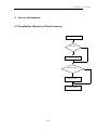
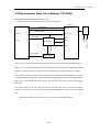
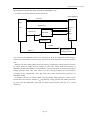
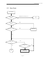
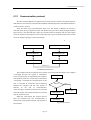
TECHNICAL AND SERVICE
MANUAL
(Romania)
CONTENTS
1
2
3
4
5
6
7
8
9
Technical characteristic. ............................................................................................1
Operational conditions ..............................................................................................1
General description ...................................................................................................1
Details .......................................................................................................................2
4.1
The structure diagram................................................................................2
4.2
Power supply.............................................................................................2
4.3
Architecture: a brief description of functional blocks ...............................3
4.4
Interfaces: the terminals ............................................................................4
Service information...................................................................................................7
5.1
Fiscalization (Replace of Fiscal memory).................................................7
5.2
ID Code and Number ................................................................................9
5.3
ECR Reset and Recovery ........................................................................10
5.4
Power Saving and CPU monitor .............................................................10
5.5
Data protection (Ram, Fiscal-Memory, OTP ROM) ...............................11
5.6
Power down process................................................................................13
5.7
Power up Initialization ............................................................................14
5.8
Main Loop...............................................................................................15
5.9
S Mode Function .....................................................................................16
5.10
Z Mode Function.....................................................................................17
5.11
Error Check .............................................................................................18
5.12
Communication protocol.........................................................................19
Error Message .........................................................................................................20
6.1
Familiar Error Information......................................................................20
6.2
System Error Information........................................................................22
Data map .................................................................................................................23
7.1
Daily Fiscal Data Map.............................................................................23
7.2
Fiscal Memory Map ................................................................................24
Element List ............................................................................................................25
IC Material ..............................................................................................................29
Technical and service manual
1 Technical characteristic.
Voltage:
220V AC/7.1V DC power supplier
DC power battery: 6V 3.2AH
Approximately power consumption
Idle power consumption
Peak current
Sleep mode current
5W
30mW
6A
0.5mA
Permissible work temperature
Data base memory
Printing mechanism
Thermal printer
Paper
-10°C~+40°C
CMOS RAM
TP201
Receipt roll (2x28 mm)
2 Operational conditions
1. The cash register shall be operated without direct sunlight, in the ambient temperature of
more than -10°C and less than +40°C.
2. The cash register shall be connected to a PSU (Power Supply Unit) supplied by the
producer (220V AC 50HZ) or to an internal battery (6V for the thermal printer version).
3. The cash register shall be operated in dust-free and dry rooms (working under high dust
concentration conditions reduces the mechanism’s life).
3 General description
The cash register has an RS232 serial interface. With which you can connect it to an external
computer or an external barcode scanner.
The device is made up of one electronic module for controlling all the cash register function:
the keyboard control, the LCD display (customer and client), printing mechanism (thermal),
the drawer, OTP-type fiscal memory and real time clock, It allows for the communication
with an external computer, a barcode scanner.
It is also provided with software. Which is a pure Win32 program, and must run in Windows
98. The software provides the cash register data (including PLU goods and Department
information) manage. It allows for data and Report (including X and Z report, Fiscal report,
Clerk report,X2 and Z2 report) to be uploaded from the cash register.
The LCD display is capable of displaying 6 characters and 8 digits. It rolls long message
from right to left with the message showing length increasing.
Page 1
Technical and service manual
4 Details
4.1 The structure diagram
Data
Printer
RAM
OTP
Fiscal
Address
Address Decode
Main CPU
Power Control CPU
Power
drawer
RS232
LCD
PC
Real time
Clock
Keyboard
Scanner
4.2 Power supply
The device has a build-in battery (6V for a thermal printing mechanism) or may be connected
to an external PSU (220V AC 50HZ) with the battery charging operation. When the external
PSU is connected and switched on, the battery is charged automatically, no matter whether
the cash register is operating or not. The cash register may also be operated when the battery
is being charged. The charging time is unlimited, which means that the cash register may be
connected to the PSU all the time.
When printing job is over and no key is pressed for a long time, the device will shut
power-consuming component and go into sleep mode until one key is pressed or
communication starts.
Page 2
Technical and service manual
4.3 Architecture: a brief description of functional blocks
Main board power input is 7.1V DC. It offers printing driver and motor driver. With DC-DC
24V is used to control drawer, and 13V is used as Fiscal-Memory program voltage. 5V supply
working voltage of system.
Main CPU connects 128K RAM and 512K OTP ROM. The first 32K RAM is used for
temporary variable, and the other is data area. The first 64K ROM is program area, and the other is
data area.
The second CPU is EM78P451. It is responsible for monitoring Main CPU, Data protection,
Fiscal Memory protection, keyboard scanning and power controlling.
Thermal printing mechanism is APS MP-205.
Fiscal Memory can be written only once. It can not be removed while working. When it’s
removed, the device will detect it and halt itself.
The RS232 is controlled by Main CPU and the highest baud rate is 115200. When the
distance is increased, the baud rate must be decreased.
The Real Time Clock IC. It can take count of year, month, day, hour, minute, second and leap
year. The cash register can access and set up the real time clock.
A LCD appropriative driving IC takes charges of it and it has backlight controller.
Page 3
Technical and service manual
4.4 Interfaces: the terminals
CN-IC:The fiscal memory connector
Jumper:
J2A,J2B
27C010,27C020,27C040:
1
VPP1
2
PRG-VCC
3
AA16
4
AA18
5
A15A
6
A17A
7
AA12
8
AA14
9
AA7
10
AA13
11
AA6
12
AA8
13
AA5
14
AA9
15
AA4
16
AA11
17
AA3
18
PRGOE
19
AA2
20
AA10
21
AA1
22
PRGCS
23
AA0
24
DD7
25
DD0
26
DD6
27
DD1
28
DD5
29
DD2
30
DD4
31
GND
32
DD3
33
LOOP1
Out
34
LOOPCHK In
CN101: Keyboard connector
1
Loop2
2
K0
3
K1
4
K2
5
K3
6
Key2
7
Key3
8
Key4
9
Key5
Out
Out
Out
Out
In
In
In
In
J1A:Off
J1B:Off J2A:On J2B:On
0V:Read-out, +13V:Programming
5V:Read-out, +6V:Programming
FM(Fiscal Memory) Address
If FM is 27C256 VPP else AA15
If FM is 27C256 PRG-VCC else AA16
Output Enable Low: Read High :Program
Chip Enable Low: Enable High: Disable
FM data
Gnd
With Pin34, Check if FM is installed or not.
Loop with Loop1 to detect keyboard is installed
Row 0
Row 1
Row 2
Row 3
Column 0
Column 1
Column 2
Column 3
Page 4
Technical and service manual
10
11
12
13
14
15
Key6
Key7
Key8
Key9
K4
Loop1
In
In
In
In
Out
Column 4
Column 5
Column 6
Column 7
Row 4
Loop with Loop2
CN102: EPM3032ALC44 programming connector
1
+3.3V
Power
2
ISP-TDI
Out
Data output
3
ISP-TDO
In
Data input1
4
ISP-TCK
Clock
5
ISP-TMS
In
Data/Command input
6
GND
CN103: LCD Display connector
1
LOOP3
2
LUMI
3
KDAT/LIT
4
LCD-CLK
5
LCD-DAT
6
P2S-LD
7
LCDWKLP
8
VDD-LCD
9
LCD-CS
10
GND2
JH1: MP205 connector
1
PRN-PS
2
VPS2
3
GND
4
+BAT2
5
+BAT2
6
PRNDAT
7
PRNDSS3
8
PRNDSS4
9
PRNDSS3
10
PGND
11
PGND
12
PGND
13
PGND
14
PRN-TH2
15
PRNDST4
16
PRNDST3
17
PRNDST4
18
M+5V
19
PRNCLK
20
PRN-LH2
21
22
BAT2
23
BAT2
24
/PRN2B
25
/PRN2A
Page 5
Technical and service manual
26
27
PRN2B
PRN2A
CN203: Drawer connector
1
P+20V
2
Drawer
3
Gnd
4
Draw-Sw
Out
CN202: Power
1
+BAT
2
PGND
3
CN1: RS232 Interface (PHONE6)
1
CTS
2
+5V
3
GND
4
RXD
5
TXD
6
RTS
Page 6
Technical and service manual
5 Service information
5.1 Fiscalization (Replace of Fiscal memory)
Go to SET mode
Tax set?
Y
N
Set tax
Set Price dot?
Set price dot
Go to S mode
Page 7
Y
Technical and service manual
1.
2.
Use [KSW/CLERK] key to select S mode
Input S mode password, then
Go to S mode
press [TOTAL] to enter S
mode
3. Use [-%],[+%] key to select
‘Set ID Code & Number’,
Has ID code & number
then press [TOTAL] key
4. According to the prompt,
N
Input ID Code (2 characters,
Set ID code & number
use [-%],[+%] to change
character, For example, input
‘AB’ and press [TOTAL]
5. According to the prompt,
Has header message
Input ID Number ( 10 digit ),
then press [TOTAL] key to set.
N
For example, input
‘1234567890’ and press
Set header message
[TOTAL]. According to the
prompt, you will be asked to
confirm the ID Code
Set fiscal mode
&number you entered. Select
1:Yes or 2:No.
6. Use [-%],[+%] key to select
Enter ID number
‘head message set’, then press
[TOTAL] key
7. according to the prompt, input
OK
the line you want to edit, then
press [TOTAL], according to the prompt, input the message no more than 24
characters. You must set the five-line head message, or you can’t enter fiscal
mode.
8. Use [-%],[+%] key to select ‘Fiscal mode setting’, then press [TOTAL] key
9. According to the prompt, input ID number which is set before, then press
[TOTAL] key
After the steps, the configuration of ECR is as followed.
ID Code and Number
AB 1234567890
Note:
1. ID Code & Number must be setup before Fiscalization
2. Header message must be set up before fiscalization.
3. Tax and price dot must be set
Page 8
Y
Y
Technical and service manual
5.2 ID Code and Number
According to the layout of Fiscal Memory, refer to “Map Of Fiscal Memory’, ID
Code and Number are placed at 1FFD8—1FFE3. Just before setting ID Code and
Number, the s/w will read the 12 bytes first, check if they are the same as set or all
blank (value FF mean blank), if not blank, and Code Number is not the same, then
error 48 occur. After set ID Code and Number, the s/w will read again to make sure it’s
be written correctly, if not correct Error 52 will occur.
Start
Input ID Code & Number
Print ID Code & Number
N
Confirm?
Y
Read ID Code & Number
Is Blank?
N
Y
Write ID Code & Number
Are Code same &
Number same?
Y
N
Y
N
Error 48
Is Write OK?
Error 52
Ok and Print
End
Page 9
Technical and service manual
5.3 ECR Reset and Recovery
1. Use [KSW/CLERK] key to select S mode, then press [TOTAL] key
2. Input S mode password, press [TOTAL] key
3. Use [-%],[+%] key to select ‘ECR reset’, then press [TOTAL] key.
4. Use [-%],[+%] key to select ‘Recovery’, then press [TOTAL] key
5. Input Time (format HHMM, HH:Hour00-24, MM:Minute00-59), press [TOTAL] key
6. Input Date (format DDMMYYYY. DD: Day MM: Month, YYYY: Year ), then press
[TOTAL] key
Note:
1. After ECR reset, Recovery must be done. Otherwise, Fiscal error will appear.
2. Recovery will restore Z-Counter ,sale-total and tax total from Fiscal.
5.4 Power Saving and CPU monitor
Battery or external power supply unit can supply this device. When the external power supply
unit is connected and switch on, the automatic battery charging begin, no matter whether the cash
register is turned on or not. It means that that battery can be charged for any time duration.
When lack of external voltage, the battery supply begin. In idle mode, the main CPU,
EPM3032ALC44, 29C020 will consume a lot of energy. It will exhaust the battery energy. So
power saving here is very important. In both power supply, since the end of a printout if no key is
pressed for 1 minute, main CPU will inform the second CPU that it’s idle now, the second will turn
the power off and then go into sleep mode. When one key is pressed or communication start, the
second CPU will wake up and turn the power on automatically.
Main CPU will communication with the second CPU per 10 ms. If the communication
between two CPU disappear for 2 second, main CPU may run abnormally, the second CPU will
reset main CPU.
Page 10
Technical and service manual
5.5 Data protection (Ram, Fiscal-Memory, OTP ROM)
DESCRIPTION OF RAM PROTECTION(15X):
1. Correlative circuit frame drawing as have been showed below:
RAM
MAIN
D0-D7 VDD
Address bus
A0 –A16
Control bus
WE
Ram WP
Control bus
EM78P451
2.We can learn clearly from the frame drawing that there are two ways about RAM protection.
3.When we do the writing operation, it is needed that the main CPU cause EM78P451 RAM
disable the writing protection, and then it can be operated the writing data operation to RAM.
4.After this, main CPU order the writing data protection valid about EM78P451RAM. So we can
conclude that there are two ways to protect the RAM writing operation, in case that programmer of
main CPU run out, the data still can be protect very well and avoid destroy because of the double
protection
5.In another hand, we can learn from the drawing that when the power is turned off suddenly
(mean no 5v power now), it can be supplied by the standby battery in order to protect the RAM
data.
Synthetically adopt the above method, we can protect the RAM data reliably.
Page 11
4.6v Battery
DECODE
CE
OE
5v
CPU
Power
DATA BUS
Technical and service manual
DESCRIPTION OF PROTECTION OF FISCAL MEMORY (15X)
1. Correlative circuit frame drawing showed as below:
Fiscal-EPROM
Data bus
D0-D7
Main
Address bus
CPU
Control bus
A0-A16
CE
OE
WE
DECODE
VPP
EM78P451
FISWP
Programming
voltage generator
PRGVCC
2.As we know Fiscal-Memory data is very important for ECR, as if appeared invalid writing it
maybe cause serious effect, so we have pay more attention about the protection of Fiscal-memory
data.
When process the writing operation to Fiscal-memory, programming voltage generator needs to
be output. While its output must be ordered by main CPU, which made Fiscal-memory of
EM78P451 disable. More addition, valid of PRGVCC of main CPU allow VPP output programming
Voltage generator, then main CPU orders to process writing protection for Fiscal-memory
according to the programming. After that main CPU orders Fiscal-memory protection of
EM78P451 enable.
According to the above it needs to output VPP programming voltage generator in order to write
the data into Fiscal-memory. Because VPP programming voltage generator has double protections
by main CPU and EM78P451, that ECR can protect Fiscal-memory data not to be invalid
effectively.
Page 12
Technical and service manual
5.6 Power down process
Check power failure at the power terminal. If power failure happens, an interrupted signal
will be send to CPU, then CPU will conduct the following process:
a.
Switch the peripheral I/O to power save mode.
b.
Backup system register to the
Power down
external RAM
c.
CPU go into power down state.
N
Data Changed?
Waiting for reset.
Y
d.
If system resumes power supply
halfway. After RESET, I/O will be
Save data
initialized and return to the last
working status.
Ram, Fiscal, OTP into Read-only state
Note: In normal working state, RAM’s Chip
Select is powered with 5V. When power
Port Close
failure, the voltage decrease to 4.6V. Then
RAM’s Chip Select will enter Disable mode.
Send Sleep Command
Such action can prevent RAM from missing.
And CPU will be forced to RESET state, this
Mark Sleep-power up Flag
prevent RAM from being affected by CPU
execution.
Lock Main CPU
Page 13
Technical and service manual
5.7 Power up Initialization
a.
b.
c.
d.
e.
f.
g.
h.
i.
j.
k.
l.
Stack set, Stack Pointer = 0xA0
Initialize Port
Timer set
Serial Initial. Baudrate = 9600, No parity, Stop Bit = 1
Working memory clear
Check the checksum of program.
If the checksum is ERROR then wait for program
update from PC.
Restore backup data
Check the RAM data
If RAM data is invalid then clear Data memory
Recovery, restore data from Fiscal memory
Go to main loop
No
Stack Set
CPU Mode Set
Port initialization
Serial Initialization
Clear working memory
Checksum
of
program right?
Yes
Restore backup data
Update loop
No
Clear data memory
RAM valid ?
Yes
Recovery
Main loop
Fig. Program Reset
Page 14
Technical and service manual
5.8 Main Loop
The device program is a software which bases of message mapping mechanism. The time is
separated by the software. The device scans the keyboard per 10ms and refresh LCD per 100ms etc.
The main loop just peek the message and translate the message, then handle the message. Only one
message is handled every loop. If no keyboard is in queue and message buffer is empty, it is
regarded as idle. In idle state, system is checked in sequence. In another word, Fiscal memory,
keyboard, display, ram, printer… will be checked by order. If any device is wrong, Exception is
raised, waiting operator to handle.
Main
Key queue is
empty ?
Idle process
Translate Key message
Message in
queue?
OFF
REG
X
Z
Main Loop
Page 15
S
Program
Technical and service manual
5.9 S Mode Function
S MODE
PASSWORD OK
?
Yes
%-, %+ key
?
No
No
Yes
Time set
Date set
Header message set
Recovery operation
ID code & number
Fiscal mode set
Error
?
Yes
Test FUN.
Error
Page 16
No
Technical and service manual
5.10
Z Mode Function
Z1 Report
No
Z mode
?
Yes
Z counter up (+1)
Head print
Drawer open
Detail Sales data print
No
Z mode
?
Yes
Daily fiscal data write
FISWRT
Z2 data update
Daily sales clear
End print
Yes
Z counter full
?
Print Z counter
full message
No
No
Z counter near full
?
Yes
Print Z counter near full
message
To MAIN Return main loop
Page 17
Indicate Fiscal
Error message on DISPLAY
Block ECR
END
Technical and service manual
5.11
Error Check
SYS CHECK
System error
Check?
ROM error, fiscal error. etc
Error
Yes
No
ID code
Check?
Fail
OK
ID number check?
Fail
Fiscal error
OK
Paper end
?
Check?
No
End
Yes
Feed Key On
?
Paper feed
Page 18
No
Technical and service manual
5.12
Communication protocol
The device adopts RS232 as its physical layer protocol with 115,200 as its highest baudrate.
With distance increased, the communication baudrate should be decreased. The default baudrate is
9,600 no parity 1 stop bit.
There are three layers communication layer here. The bottom is RS232, the second is
data-link-layer, the top is application-layer. The bottom layer provides a cheap and high-reliability
physical layer. The data-link-layer make sure the data between computer and the cash register
correctly transferred. The top layer use 256 bytes data and 3 bytes command as basic unit. In other
word, the length of package is fixed at 259 bytes.
1
256B data & 3B command
256B data & 3B command
Encode &Decode
Encode &Decode
RS232
RS232
Connector
Communication Layer
The computer and the cash register has a relation of principal and subordinate. The computer
is principal and the cash register is subordinate.
Connect
Every communication is originated by the computer.
The computer sends out a “connecting” command. In
“connecting” command, the communication of this
time is included. If connected, data transferring
No
Allow?
between the computer and the cash register is
allowed. At the end of communication,
Yes
“Disconnecting” command is sent from the computer.
Error report
The cash register will reset the baudrate to 9,600 and
Data transfer
stop the communication.
When the cash register has account and has
been not committed yet. The communication is
Disconnect
allowed. The cash register will send “not allowed” to
Fig Communication
the computer.
Page 19
Technical and service manual
6 Error Message
6.1 Familiar Error Information
Format of familiar error information is ERR X
Error code and description
Error number
01
02
03
04
05
06
07
08
09
10
11
12
13
14
15
16
17
18
19
20
21
22
23
24
25
26
27
28
29
30
31
description
this function key can’t use in X, Z, SET, S mode
ECR can’t work without input clerk code
digit input error
clerk no.invalid
quantity invalid
prohibit to correct
prohibit discount
prohibit +%
prohibit -%
prohibit void
press price key invalid
press FC key invalid
communicate with FTP fail
prohibit to press cash key
prohibit to press credit key
prohibit to press check key
please clear account
password error
set time error
input barcode error
input date error
write FLASH error
prohibit to print daily report
50 PLU at 1 receipt at most
no hardware reset
barcode not yet download
NAND FLASH not exist or defective
waste book area full
password error
daily report not be cleared
PLU area will be full
Page 20
Technical and service manual
32
33
34
35
36
37
38
39
40
41
42
43
44
45
46
47
48
49
50
51
52
53
54
55
56
57
58
59
60
61
62
63
64
65
66
67
68
69
70
71
72
73
74
75
input data error
this clerk no. has existed
clerk memory space full
invalid weight
ECR is on sale
cash in drawer overflows
super password error
cash in drawer is not enough
R/A amount overflows
P/O amount overflows
PLU is not found
sale price invalid
price error
PLU report overflows
fiscal ID must be 2 characters
fiscal ID& code have been set
fiscal code invalid
tax ID format error
tax ID has been set
tax ID error
writing fiscal memory failed
tax rate invalid
dept space is full
tax rate space is full
fiscal code error
fiscal memory full
write fiscal memory error (in z report)
ECR isn’t in fiscal mode
PLU can’t return
FM READ ONLY
printer no paper
printer 1 no paper
printer 2 no paper
member card input error
plomp command error
pay credit error
HARDWARE RESET ERROR
PLU recycle error
recycle index error
recycle unit price error
function error in recycle mode
no set fis code & num
no set tax ID
no set tax rate
Page 21
Technical and service manual
76
77
78
79
fiscal memory was exchange
header can’t be set in fiscal mode
head message aren’t set ok
no FM or address or data bus short
6.2 System Error Information
Error code
1FE
Error description
device error
Page 22
Technical and service manual
7 Data map
7.1 Daily Fiscal Data Map
Z1 Count
4 Digits
2 bytes(BIN)
Amount of Tax A
10 Digits
5 bytes(BIN)
Amount of Tax B
10 Digits
5 bytes(BIN)
Amount of Tax C
10 Digits
5 bytes(BIN)
Amount of Tax D
10 Digits
5 bytes(BIN)
Amount of Tax E
10 Digits
5 bytes(BIN)
Time(hour/minute)
4 Digits
2 bytes(BCD)
Reserve
6 Digits
3 bytes
10 Digits
5 bytes(BIN)
Date(Day/Month/Year)
6 Digits
3 bytes(BCD)
Fiscal receipt count
4 Digits
2 bytes(BIN)
Index of Tax rate table
2 Digits
1 bytes
2 Digits
1 bytes
2 Digits
1 byte
Sales Total
Reserve
Check sum
Total:45 bytes
Page 23
Technical and service manual
7.2 Fiscal Memory Map
Start Address
00000
00004
Content
Description
AA,55,AA,55
Fiscal identification flag bytes
Reserve
00300
Daily fiscal data, totally has 1830 daily fiscal data record. Every
daily fiscal data needs 45 bytes, so 1830 * 45 bytes fiscal memory is
occupied
Daily Fiscal Data ( 45 )
144AE
1F650
Reserve
200 Recovery data, total 200 * ( 2+5 ) = 1400
Z Counter( 2 )
Time(hhmmDDMMYY)( 5 )
1FBD0
30 Tax Rate, total 30*(10+2+5) = 510
Tax Rate(10)
Z Counter(2)
Time(hhmmDDMMYY)(5)
1FDDC
1FE7C
1FFC0
1FFC1
Header message
Reserve
Mode flag
Reserve
1FFD2
Decimal Position
1FFD8
1FFE4
1FFFC
FF:Training mode, 5A:Fiscal mode
Fiscal mode set time ( 5 )
1FFC6
1FFD3
5 * 32 = 160
Store the date of fiscal mode setting. (DDMMYY hhmm)
0:w/o decimal, 2:decimal position = 2
Reserve
Fiscal Code(2) & Number(10)
Reserve
‘PECR’
Indicate Fiscal type
Page 24
Technical and service manual
8 Element List
Printer Board
ITEM
1
QTY
1
DESCRIPTION
EPCRMMYLAB5040315A
REFERENCE-DESIGNATOR
PCB
2
3
4
5
6
7
8
1
1
1
2
1
2
1
MCRMC08PH04P15000
MCR2C05FFC27P12500
220uF/16V
47K/SMD0805
104/SMD0805
DTC114EN3/SOT23
FFC18,180/1.0mm
JH2
C20
R126,R125
C18
Q1,Q2
J-TP201
9
1
O -30MM
Display---shop
ITEM
1
2
3
4
5
6
7
8
QTY
1
1
2
1
2
1
1
1
DESCRIPTION
V=104/SMD0805
V=PECRLCD
V=LED-2
V=BC817-40
V=20R/SMD0805
V=1K5/SMD0805
V=47K/SMD0805
V=98L50/DICE1
REFERENCE-DESIGNATOR
C1
LCD1
LED1,LED2
Q1
R1,R2
R7
R8
U1
Display---client
ITEM
1
2
3
4
5
6
7
8
QTY
1
1
2
1
2
1
1
1
DESCRIPTION
V=104/SMD0805
V=PECRLCD
V=LED-2
V=BC817-40
V=20R/SMD0805
V=1K5/SMD0805
V=47K/SMD0805
V=98L50/DICE1
REFERENCE-DESIGNATOR
C1
LCD1
LED1,LED2
Q1
R1,R2
R7
R8
U1
9
1
V=JMP
J2
10
1
V=FFC10,180/1.0MM
CN2
ITEM QTY DESCRIPTION
REFERENCE-DESIGNATOR
1
1
V=EPCRMNPTMBC-041109B
PCB
2
1
V= radiator 12*6mm
Page 25
Technical and service manual
3
4
5
6
7
8
9
10
11
12
13
14
15
16
17
18
1
2
1
3
1
1
1
1
1
1
2
1
1
2
1
2
V=MS621/3.0V/4mA
V=105/SMD0805
V=47uF/35V
V=220uF/10V
V=101/SMD0603
V=103/50V/MC/DIP
V=470uF/10V
V=220uF/16V
V=2200uF/35V
V=391/SMD0603
V=1000uF/10V
V=10uF/10V
V=47uF/35V/CDZ11
V=5P/NPO/SMD0603
V=4.7uF/16V
V=12P/SMD0603
BAT1
C1,BC1
C10
C13,C28,C29
C14
C15
C19
C20
C24
C26
C33,C35
C37
C38
C40,C41
C42
C47,C48
19
20
21
22
23
24
25
26
27
28
29
9
41
1
3
1
1
1
3
3
1
2
V=102/SMD0603
V=104/SMD0603
V=CHOKE/330uH/0.3A
V=1N4148/SMD1206
V=HBAT54C/SOT-23
V=HBAT54A/SOT-23
V=HBAT54/SOT-23
V=1N4001/DO41
V=1N5819/DO41
V=HBAT54S/SOT-23
V=3.15Amp/Slow
CK1
D1,D3,D4
D13
D16
D17
D2,D6,D7
D8,D14,D15
D9
FUSE1,FUSE3
30
31
32
33
34
35
36
37
38
39
40
41
42
43
44
45
46
1
28
14
3
2
2
1
1
1
1
1
1
1
5
2
1
1
V=1.2Amp/Slow
V=1uH/SMD0805
V=RH3.5X6X0.8
V=G6H-06010051
V=H2N7002/SOT23
V=HBA114ES6R/SOT363
V=HBC114ES6R/SOT363
V=HMBT3906/SOT23
V=PMOS/CEM4435/SOIC8
V=HSB772/TO126ML
V=HM772/SOT89
V=DTC114EN3/SOT23
V=DTA144EN3/SOT23
V=HMBT3904/SOT23
V=HM5551/SOT89
V=2SC2873Y/SOT89
V=1.8K/SMD0603
FUSE2
L8,L14,L?
Q1,Q18
Q11,Q28
Q12
Q15
Q16
Q17
Q2
Q23
Q4
Q6,Q14,Q21,Q27,Q22
Q7,Q9
Q8
R?
Page 26
Technical and service manual
47
48
49
50
51
52
53
54
55
56
57
58
59
60
61
62
63
64
65
66
67
68
69
70
71
72
73
74
75
76
77
78
79
80
81
82
83
84
85
86
87
88
89
90
1
1
1
5
3
1
1
1
1
3
1
3
1
1
2
3
4
1
6
3
1
1
3
2
1
2
3
2
2
1
1
1
2
6
1
2
2
1
4
1
1
2
1
1
V=7k5/SMD0603
V=680R/SMD0603
V=5K1/SMD0603
V=100R/SMD0805
V=510K/SMD0603
V=30K/SMD0603
V=8K2/SMD0603
V=390R/SMD0603
V=10M/SMD0603
V=1K5/SMD0603
V=442K/1%/SMD0603
V=220R/SMD0603
V=75R/SMD0805
V=1K00/1%/SMD0603
V=4K70/1%/SMD0603
V=1M/1%/SMD0805
V=10K/SMD0603
V=7K50/1%/SMD0603
V=47K/SMD0603
V=100K/1%/SMD0603
V=270R/2W
V=768K/1%/SMD0603
V=1K/SMD0603
V=27K/SMD0603
V=3R9/SMD0805
V=1R/SMD0805
V=330R/SMD0603
V=4K7/SMD0603
V=180R/SMD0603
V=10R/SMD0805
V=22K/SMD0603
V=150R/SMD0603
V=910K/SMD0603
V=100K/SMD0603
V=62K/1%/SMD0603
V=1M/SMD0805
V=470R/SMD0603
V=680K/SMD0603
V=0R11/SMD0805
V=3K/SMD0805
V=470R/SMD0603*4
V=10K/SMD0603*4
V=100R/SMD0603*4
V=SW3PIN/4.0mm
R108
R113
R12
R13,R31,R94,R106,R107
R17,R40,R93
R20
R23
R24
R29
R3,R65,R67
R32
R33,R43,R78
R34
R35
R36,R45
R37,R60,R76
R38,R46,R47,R54
R44
R5,R6,R30,R53,R59,R109
R51,R57,R58
R52
R55
R61,R71,R112
R62,R97
R66
R68,R70
R7,R9,R69
R72,R74
R73,R98
R75
R77
R773
R79,R96
R8,R10,R14,R21,R22,R99
R80
R81,R82
R84,R86
R87
R88,R89,R100,R101
R92
RN1
RN2,RN4
RN3
SWITCH1
Page 27
Technical and service manual
91
92
93
94
95
96
97
98
99
100
101
102
103
104
105
106
107
108
109
110
111
112
113
114
115
116
117
118
119
120
121
122
123
124
125
126
127
128
129
130
1
1
1
1
2
1
1
1
1
1
1
1
1
1
1
1
1
1
1
1
4
1
1
1
1
1
1
1
1
1
1
1
1
1
1
1
1
1
1
3
V=74HCT164/SOIC14
V=74AHC08/TSSOP14
V=CD4066BC/SOIC14
V=LM324/SOIC14
V=LM393/SOIC8
V=BA6846VF/TSSOP14
V=BS62LV1027SC/SOIC32
V=KA34063A/SOIC8
V=XC62FP3302PR/SOT89
V=XC62GR5012PR/SOT895
V=XC61CN5602MR/SOT23
V=XC62EP5002MR/SOT25
V=HT1381/SOIC8
V=XC6201P352PR/SOT89
V=74HCT32PW/TSSOP14
V=HT7044A-1/SOT25
V=98CP49/PQFP100
V=EM78P451Q
V=W29C020/PLCC32
V=XC61CN4502MR/SOT23
V=74AHCT273PW/TSSOP20
V=74LVC138/TSSOP16
V=EPM3032ATC/TQFP44
V=14M7456Hz/ZTT
V=36M864Hz/ZTT
V=32K768Hz
V=24V/0.5W/SMD1206
V=3PIN/2.54MM
V=CONN PCB 17x2
V=DC-JACK/2.75MM
V=EH02/90
V=FFC10,180/1.0mm
V=FFC13,180/1.0mm
V=FFC27/180/1.00mm
V=PH02,90
V=PH04,180
V=PHONE4C
V=PHONE6C
V=XH02.90
V=JMP
U1
U14
U15
U16
U17,U30
U19
U2
U20
U21
U22
U23B
U24
U26
U27A
U28
U29
U3
U4
U5
U6
U7,U10,U11,U12
U8
U9
X1
X2
Y1
ZD1
J5
CN-IC1
DC-IN1
CN-BZ1
CN104B
CN101
J_MP205
J3
J4
J1
CN1
BATTERY
RAM-VCC1,J2B,J2A
Page 28
Technical and service manual
9 IC Material
A.
B.
C.
D.
E.
F.
G.
H.
I.
J.
K.
L.
M.
N.
O.
P.
Q.
R.
S.
98CP49
EM78P451
EPM3032ATC
4066
SN74HC138D
SN74HC04D
SN74AHC08D
Hcc4052b
BSI1027
AT27C040
HT1381
KA34063
XC62EP
XC62FP5002
XC62FP3302
LM393
74HCT164
SN74AHC273
LM324
Main CPU
Secondary CPU
Programmable Logic Device Family
Quad bilateral switch
decoder
Hex inverter
And gate
analog multiplexers demultiplexers
128K x 8 CMOS Static RAM
OTP ROM
Serial timekeeper Chip
DC-to-DC Converter Control Circuit
Boosting Voltage Regulators
Boosting Voltage Regulators
Boosting Voltage Regulators
Low Power Low Offset Voltage Quad Comparators
8-Bit Serial-in/Parallel-out Shift Register
OCTAL D-TYPE FLIP-FLOPS WITH CLEAR
Quadruple Operational Amplifiers
Page 29


![ZXmore-V11-ConstructionKit [1144.78] KB](http://vs1.manualzilla.com/store/data/005859049_1-e30fafda14586d16f36a324828eeb8d9-150x150.png)