1
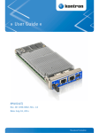
AM5030
Double Full-size AMC Module based on the
Intel® Xeon® LC5518 Processor with the
Intel® 3420 Chipset
Doc. ID: 1036-3302, Rev. 1.0
June 10, 2010
If it’s embedded, it’s Kontron.
PRELIMINARY
» User Guide «
Preface
AM5030
Revision History
Publication Title: AM5030: Double Full-size AMC Module based on the Intel® Xeon®
LC5518 Processor with the Intel® 3420 Chipset
Doc. ID: 1036-3302
Rev.
PRELIMINARY
1.0
Brief Description of Changes
Date of Issue
Initial issue
10-Jun-2010
Imprint
Kontron Modular Computers GmbH may be contacted via the following:
MAILING ADDRESS
TELEPHONE AND E-MAIL
Kontron Modular Computers GmbH
+49 (0) 800-SALESKONTRON
Sudetenstraße 7
[email protected]
D - 87600 Kaufbeuren Germany
For further information about other Kontron products, please visit our Internet web site:
www.kontron.com.
Disclaimer
Copyright © 2010 Kontron AG. All rights reserved. All data is for information purposes only and
not guaranteed for legal purposes. Information has been carefully checked and is believed to
be accurate; however, no responsibility is assumed for inaccuracies. Kontron and the Kontron
logo and all other trademarks or registered trademarks are the property of their respective owners and are recognized. Specifications are subject to change without notice.
Page ii
ID 1036-3302, Rev. 1.0
AM5030
Preface
Revision History .........................................................................................................ii
Imprint ........................................................................................................................ii
Disclaimer ..................................................................................................................ii
Table of Contents ...................................................................................................... iii
List of Tables ............................................................................................................ vii
List of Figures ...........................................................................................................ix
Proprietary Note ........................................................................................................xi
Trademarks ...............................................................................................................xi
Environmental Protection Statement .........................................................................xi
Explanation of Symbols ........................................................................................... xii
For Your Safety ....................................................................................................... xiii
Two Year Warranty ...................................................................................................xv
1.
Introduction ............................................................................. 1 - 3
1.1 Board Overview ....................................................................................... 1 - 3
1.2 Board-Specific Information ...................................................................... 1 - 4
1.3 System Relevant Information .................................................................. 1 - 5
1.4 Board Diagrams ...................................................................................... 1 - 5
1.4.1
Functional Block Diagram ............................................................... 1 - 5
1.4.2
Front Panel ..................................................................................... 1 - 7
1.4.3
Board Layout .................................................................................. 1 - 8
1.5 Technical Specification ............................................................................ 1 - 9
1.6 Standards .............................................................................................. 1 - 15
1.7 Related Publications ............................................................................. 1 - 16
2.
Functional Description ........................................................... 2 - 3
2.1 Processor ................................................................................................ 2 - 3
2.2 Memory ................................................................................................... 2 - 4
2.3 Intel® 3420 Chipset ................................................................................. 2 - 4
2.4 Timer ....................................................................................................... 2 - 5
2.5 Watchdog Timer ...................................................................................... 2 - 5
2.6 Battery ..................................................................................................... 2 - 5
2.7 Power Monitor and Reset Generation ..................................................... 2 - 5
ID 1036-3302, Rev. 1.0
Page iii
PRELIMINARY
Table of Contents
Preface
AM5030
2.8 FLASH Memory .......................................................................................2 - 5
2.8.1
SPI FLASH for uEFI BIOS ..............................................................2 - 5
2.8.2
Serial ATA Flash Module (Optional) ................................................2 - 6
2.9 Trusted Platform Module 1.2 (On Request) .............................................2 - 6
2.10 Board Interfaces ......................................................................................2 - 7
2.10.1 Front Panel LEDs ............................................................................2 - 7
2.10.2 Module Handle .............................................................................. 2 - 11
2.10.3 General Purpose DIP Switches SW2 and SW3 ............................2 - 12
2.10.4 Debug Interface .............................................................................2 - 12
2.10.5 USB Host Interfaces ......................................................................2 - 13
PRELIMINARY
2.10.6 Serial Port .....................................................................................2 - 13
2.10.7 Serial ATA Interfaces .....................................................................2 - 14
2.10.8 PCI Express Interface ...................................................................2 - 14
2.10.9 Gigabit Ethernet Interfaces ...........................................................2 - 14
2.10.9.1
Dual Gigabit Ethernet Connector ..........................................2 - 15
2.10.10 10 Gigabit Ethernet XAUI Interfaces .............................................2 - 16
2.10.11 Graphics Interface .........................................................................2 - 16
2.10.11.1 VGA Connector J6 ................................................................2 - 16
2.11 AMC Interconnection .............................................................................2 - 17
2.11.1 Fabric Interface .............................................................................2 - 17
2.11.2 Synchronization Clock Interface ....................................................2 - 19
2.11.3 System Management Interface .....................................................2 - 19
2.11.4 JTAG Interface ..............................................................................2 - 19
2.11.5 Module Power Interface ................................................................2 - 19
2.11.6 Pinout of AMC Card-edge Connector J1 .......................................2 - 20
2.12 Module Management .............................................................................2 - 24
2.12.1 Module Management Controller ....................................................2 - 24
2.12.2 MMC Signals Implemented on the AM5030 ..................................2 - 25
3.
Installation ................................................................................ 3 - 3
3.1 Safety Requirements ...............................................................................3 - 3
3.2 Module Handle Positions .........................................................................3 - 4
3.3 Hot Swap Procedures ..............................................................................3 - 5
Page iv
ID 1036-3302, Rev. 1.0
AM5030
Preface
3.3.1
Hot Swap Insertion ......................................................................... 3 - 5
3.3.2
Hot Swap Extraction ....................................................................... 3 - 7
3.4 Installation of Peripheral Devices ............................................................ 3 - 8
3.4.1
Installation of USB Devices ............................................................ 3 - 8
3.4.2
SATA Flash Module Installation (Optional) ..................................... 3 - 8
3.4.3
Battery Replacement ...................................................................... 3 - 8
3.5 Software Installation ................................................................................ 3 - 9
Configuration ........................................................................... 4 - 3
4.1 DIP Switches SW2 and SW3 Configuration ............................................ 4 - 3
4.2 I/O Address Map ..................................................................................... 4 - 5
4.3 AM5030-Specific Registers ..................................................................... 4 - 6
4.3.1
Status Register 0 (STAT0) .............................................................. 4 - 6
4.3.2
Control Register 0 (CTRL0) ............................................................ 4 - 7
4.3.3
Control Register 1 (CTRL1) ............................................................ 4 - 7
4.3.4
Device Protection Register (DPROT) ............................................. 4 - 8
4.3.5
Reset Status Register (RSTAT) ...................................................... 4 - 9
4.3.6
Board Interrupt Configuration Register (BICFG) ........................... 4 - 10
4.3.7
Board ID High Byte Register (BIDH) ............................................. 4 - 10
4.3.8
Board and PLD Revision Register (BREV) ................................... 4 - 11
4.3.9
Geographic Addressing Register (GEOAD) ................................. 4 - 11
4.3.10 Watchdog Timer Control Register (WTIM) ................................... 4 - 12
4.3.11 Board ID Low Byte Register (BIDL) .............................................. 4 - 14
4.3.12 User-Specific LED Configuration Register (LCFG) ....................... 4 - 15
4.3.13 User-Specific LED Control Register (LCTRL) ............................... 4 - 16
4.3.14 MMC Serial Over LAN Configuration Register (ISOL) .................. 4 - 17
4.3.15 MMC Clock E-Keying Configuration Register (ICKEY) ................. 4 - 17
4.3.16 MMC AMC E-Keying Configuration Register 0 (IAKEY0) ............. 4 - 18
4.3.17 MMC AMC E-Keying Configuration Register 1 (IAKEY1) ............. 4 - 19
4.3.18 MMC Controller Status Register 0 (ICSTA0) ................................ 4 - 20
4.3.19 MMC Controller Status Register 1 (ICSTA1) ................................ 4 - 21
4.3.20 MMC Reset Status Register (IRSTA) ............................................ 4 - 22
4.3.21 IPMI Keyboard Control Style Interface ......................................... 4 - 22
ID 1036-3302, Rev. 1.0
Page v
PRELIMINARY
4.
Preface
5.
AM5030
Power Considerations ............................................................. 5 - 3
5.1 AM5030 Voltage Ranges .........................................................................5 - 3
5.2 Carrier Power Requirements ...................................................................5 - 3
5.2.1
Payload Power ................................................................................5 - 3
5.2.2
Payload and MMC Voltage Ramp ...................................................5 - 4
5.2.3
Module Management Power Consumption .....................................5 - 4
5.3 Payload Power Consumption of the AM5030 ..........................................5 - 4
5.4 Power Consumption of AM5030 Accessories ..........................................5 - 6
5.5 Power Saving Methods ............................................................................5 - 6
PRELIMINARY
5.6 IPMI FRU Payload Power Consumption ..................................................5 - 7
5.7 Payload Start-Up Current of the AM5030 ................................................5 - 7
6.
Thermal Considerations ......................................................... 6 - 3
6.1 Board Thermal Monitoring .......................................................................6 - 3
6.2 Processor Thermal Monitoring .................................................................6 - 3
6.2.1
Adaptive Thermal Monitor ...............................................................6 - 4
6.2.1.1
Frequency/VID Control ...........................................................6 - 4
6.2.1.2
Clock Modulation ....................................................................6 - 5
6.2.2
Catastrophic Cooling Failure Sensor ...............................................6 - 5
6.3 System Airflow .........................................................................................6 - 6
A.
6.3.1
Thermal Characteristic Diagram for the AM5030 ............................6 - 8
6.3.2
Airflow Impedance ...........................................................................6 - 9
6.3.3
Airflow Paths .................................................................................6 - 10
SATA Flash Module ................................................................ A - 3
A.1 Technical Specifications ......................................................................... A - 3
A.2 SATA Flash Module Layout .................................................................... A - 4
Page vi
ID 1036-3302, Rev. 1.0
AM5030
Preface
1-1
System Relevant Information ................................................................... 1 - 5
1-2
AM5030 Main Specifications .................................................................... 1 - 9
1-3
Standards ............................................................................................... 1 - 15
1-4
Related Publications .............................................................................. 1 - 16
2-1
Features of the Intel® Xeon® LC5518 Processor ................................... 2 - 4
2-2
Module Management LEDs Function ....................................................... 2 - 8
2-3
User-Specific LEDs Function ................................................................... 2 - 9
2-5
POST Code Sequence .......................................................................... 2 - 10
2-6
POST Code Example ............................................................................. 2 - 10
2-4
Watchdog and Thermal Status LEDs ..................................................... 2 - 10
2-7
Module Handle Positions ....................................................................... 2 - 11
2-8
DIP Switch SW2 Functions .................................................................... 2 - 12
2-9
DIP Switch SW3 Functions .................................................................... 2 - 12
2-10
USB Connectors J3/J4 Pinout ............................................................... 2 - 13
2-11
Serial Con. J5 (COM1) Pinout ............................................................... 2 - 13
2-12
Pinout of the Dual Gigabit Ethernet Connector J2A/B ........................... 2 - 15
2-13
D-Sub VGA Connector J6 Pinout ........................................................... 2 - 16
2-14
Pinout of AMC Card-edge Connector J1 ............................................... 2 - 20
2-15
Reserved Pins Description ..................................................................... 2 - 23
2-16
Extended Options Region Single-Ended Pins Description .................... 2 - 23
2-17
JTAG Pins Description ........................................................................... 2 - 23
2-18
Processor and Chipset Supervision ....................................................... 2 - 25
2-19
AMC-Specific Signals ............................................................................ 2 - 25
2-20
Onboard Power Supply Supervision ...................................................... 2 - 25
2-21
Temperature Signals .............................................................................. 2 - 26
4-1
Configuration of DIP Switch SW2, Switches 1 and 2 ............................... 4 - 3
4-2
Configuration of DIP Switch SW2, Switches 3 and 4 ............................... 4 - 4
4-3
DIP Switch SW3 Configuration ................................................................ 4 - 4
4-4
I/O Address Map ...................................................................................... 4 - 5
4-5
Status Register 0 (STAT0) ....................................................................... 4 - 6
4-6
Control Register 0 (CTRL0) ..................................................................... 4 - 7
4-7
Control Register 1 (CTRL1) ..................................................................... 4 - 7
ID 1036-3302, Rev. 1.0
Page vii
PRELIMINARY
List of Tables
PRELIMINARY
Preface
AM5030
4-8
Device Protection Register (DPROT) ....................................................... 4 - 8
4-9
Reset Status Register (RSTAT) ................................................................ 4 - 9
4-10
Board Interrupt Configuration Register (BICFG) .................................... 4 - 10
4-11
Board ID High Byte Register (BIDH) ...................................................... 4 - 10
4-12
Board and PLD Revision Register (BREV) ............................................ 4 - 11
4-13
Geographic Addressing Register (GEOAD) ........................................... 4 - 11
4-14
Watchdog Timer Control Register (WTIM) ............................................. 4 - 13
4-15
Board ID Low Byte Register (BIDL) ........................................................ 4 - 14
4-16
User-Specific LED Configuration Register (LCFG) ................................ 4 - 15
4-17
User-Specific LED Control Register (LCTRL) ........................................ 4 - 16
4-18
MMC Serial over LAN Configuration Register (ISOL) ............................ 4 - 17
4-19
MMC Clock E-Keying Configuration Register (ICKEY) .......................... 4 - 17
4-20
MMC AMC E-Keying Configuration Register 0 (IAKEY0) ...................... 4 - 18
4-21
MMC AMC E-Keying Configuration Register 1 (IAKEY1) ...................... 4 - 19
4-22
MMC Controller Status Register 0 (ICSTA0) .......................................... 4 - 20
4-23
MMC Controller Status Register 1 (ICSTA1) .......................................... 4 - 21
4-24
MMC Reset Status Register (IRSTA) ..................................................... 4 - 22
5-1
DC Operational Input Voltage Ranges ..................................................... 5 - 3
5-2
AM5030 in EFI Shell Mode ....................................................................... 5 - 5
5-3
AM5030 with Intel MSTRESS .................................................................. 5 - 5
5-4
AM5030 with Win. 2008 Server, 64-bit, Idle Mode ................................... 5 - 5
5-5
AM5030 with Win. 2008 Server, 64-bit, 60% Processor Workload ........... 5 - 5
5-6
AM5030 with Win. 2008 Server, 64-bit, TDP Processor Workload ........... 5 - 5
5-7
Power Consumption of AM5030 Accessories .......................................... 5 - 6
5-8
Power Saving Features ............................................................................ 5 - 6
5-9
IPMI FRU Payload Power Consumption .................................................. 5 - 7
5-10
Payload Start-Up Current of the AM5030 ................................................. 5 - 7
6-1
AM5030 Airflow Impedance by Zone [N/m²] ............................................. 6 - 9
6-2
AM5030 Airflow Impedance by Zone [inches H2O] ................................ 6 - 10
A-1
SATA Flash Module Main Specifications ................................................. A - 3
Page viii
ID 1036-3302, Rev. 1.0
AM5030
Preface
1-1
AM5030 Functional Block Diagram .......................................................... 1 - 6
1-2
AM5030 Front Panel ............................................................................... 1 - 7
1-3
AM5030 Board Layout (Top View) ........................................................... 1 - 8
1-4
AM5030 Board Layout (Bottom View) ...................................................... 1 - 8
2-1
Front Panel LEDs ..................................................................................... 2 - 7
2-2
Module Handle Positions ....................................................................... 2 - 11
2-3
USB Connectors J3/J4 ........................................................................... 2 - 13
2-4
Serial Con. J5 (COM1) ........................................................................... 2 - 13
2-5
Dual Gigabit Ethernet Connector J2A/B ................................................ 2 - 15
2-6
D-Sub VGA Con. J6 ............................................................................... 2 - 16
2-7
AM5030 Port Mapping ........................................................................... 2 - 18
3-1
Module Handle Positions ......................................................................... 3 - 4
4-1
DIP Switches SW2 and SW3 ................................................................... 4 - 3
6-1
AM5030 with ® Xeon® LC5518 Processor, 1.73 GHz ............................ 6 - 8
6-2
AM5030 Airflow Impedance ..................................................................... 6 - 9
6-3
Thermal Zones of the AM5030 Module .................................................. 6 - 10
A-1
SATA Flash Module Layout (Bottom View) .............................................. A - 4
ID 1036-3302, Rev. 1.0
Page ix
PRELIMINARY
List of Figures
PRELIMINARY
Preface
AM5030
This page has been intentionally left blank.
Page x
ID 1036-3302, Rev. 1.0
AM5030
Preface
Proprietary Note
This document contains information proprietary to Kontron. It may not be copied or transmitted by any means, disclosed to others, or stored in any retrieval system or media without the
prior written consent of Kontron or one of its authorized agents.
The information contained in this document is, to the best of our knowledge, entirely correct.
However, Kontron cannot accept liability for any inaccuracies or the consequences thereof, or
for any liability arising from the use or application of any circuit, product, or example shown in
this document.
Trademarks
This document may include names, company logos and trademarks, which are registered
trademarks and, therefore, proprietary to their respective owners.
Environmental Protection Statement
This product has been manufactured to satisfy environmental protection requirements where
possible. Many of the components used (structural parts, printed circuit boards, connectors,
batteries, etc.) are capable of being recycled.
Final disposition of this product after its service life must be accomplished in accordance with
applicable country, state, or local laws or regulations.
ID 1036-3302, Rev. 1.0
Page xi
PRELIMINARY
Kontron reserves the right to change, modify, or improve this document or the product
described herein, as seen fit by Kontron without further notice.
Preface
AM5030
Explanation of Symbols
Caution, Electric Shock!
This symbol and title warn of hazards due to electrical shocks (> 60V)
when touching products or parts of them. Failure to observe the precautions indicated and/or prescribed by the law may endanger your
life/health and/or result in damage to your material.
Please refer also to the section “High Voltage Safety Instructions” on
the following page.
Warning, ESD Sensitive Device!
PRELIMINARY
This symbol and title inform that electronic boards and their components are sensitive to static electricity. Therefore, care must be taken
during all handling operations and inspections of this product, in
order to ensure product integrity at all times.
Please read also the section “Special Handling and Unpacking
Instructions” on the following page.
Warning!
This symbol and title emphasize points which, if not fully understood
and taken into consideration by the reader, may endanger your health
and/or result in damage to your material.
Note ...
This symbol and title emphasize aspects the reader should read
through carefully for his or her own advantage.
Page xii
ID 1036-3302, Rev. 1.0
AM5030
Preface
For Your Safety
Your new Kontron product was developed and tested carefully to provide all features necessary to ensure its compliance with electrical safety requirements. It was also designed for a
long fault-free life. However, the life expectancy of your product can be drastically reduced by
improper treatment during unpacking and installation. Therefore, in the interest of your own
safety and of the correct operation of your new Kontron product, you are requested to conform
with the following guidelines.
High Voltage Safety Instructions
All operations on this device must be carried out by sufficiently skilled
personnel only.
Caution, Electric Shock!
Before installing any piggybacks or carrying out maintenance operations always ensure that your mains power is switched off.
Serious electrical shock hazards can exist during all installation,
repair and maintenance operations with this product. Therefore,
always unplug the power cable and any other cables which provide
external voltages before performing work.
Special Handling and Unpacking Instructions
ESD Sensitive Device!
Electronic boards and their components are sensitive to static electricity. Therefore, care must be taken during all handling operations
and inspections of this product, in order to ensure product integrity at
all times.
Warning!
This product has gold conductive fingers which are susceptible to contamination. Take care not to touch the gold conductive fingers of the
AMC Card-edge connector when handling the board.
Failure to comply with the instruction above may cause damage to the
board or result in improper system operation.
Do not handle this product out of its protective enclosure while it is not used for operational purposes unless it is otherwise protected.
Whenever possible, unpack or pack this product only at EOS/ESD safe work stations. Where
a safe work station is not guaranteed, it is important for the user to be electrically discharged
before touching the product with his/her hands or tools. This is most easily done by touching a
metal part of your system housing.
ID 1036-3302, Rev. 1.0
Page xiii
PRELIMINARY
Warning!
Preface
AM5030
It is particularly important to observe standard anti-static precautions when changing piggybacks, ROM devices, jumper settings etc. If the product contains batteries for RTC or memory
backup, ensure that the board is not placed on conductive surfaces, including anti-static plastics or sponges. They can cause short circuits and damage the batteries or conductive circuits
on the board.
General Instructions on Usage
PRELIMINARY
In order to maintain Kontron’s product warranty, this product must not be altered or modified in
any way. Changes or modifications to the device, which are not explicitly approved by Kontron
and described in this manual or received from Kontron’s Technical Support as a special handling instruction, will void your warranty.
This device should only be installed in or connected to systems that fulfill all necessary technical and specific environmental requirements. This applies also to the operational temperature
range of the specific board version, which must not be exceeded. If batteries are present, their
temperature restrictions must be taken into account.
In performing all necessary installation and application operations, please follow only the instructions supplied by the present manual.
Keep all the original packaging material for future storage or warranty shipments. If it is necessary to store or ship the board, please re-pack it as nearly as possible in the manner in which
it was delivered.
Special care is necessary when handling or unpacking the product. Please consult the special
handling and unpacking instruction on the previous page of this manual.
Page xiv
ID 1036-3302, Rev. 1.0
AM5030
Preface
Two Year Warranty
Kontron warrants their own products, excluding software, to be free from manufacturing and
material defects for a period of 24 consecutive months from the date of purchase. This warranty is not transferable nor extendible to cover any other users or long-term storage of the
product. It does not cover products which have been modified, altered or repaired by any
other party than Kontron or their authorized agents. Furthermore, any product which has
been, or is suspected of being damaged as a result of negligence, improper use, incorrect
handling, servicing or maintenance, or which has been damaged as a result of excessive current/voltage or temperature, or which has had its serial number(s), any other markings or
parts thereof altered, defaced or removed will also be excluded from this warranty.
If the customer’s eligibility for warranty has not been voided, in the event of any claim, he may
return the product at the earliest possible convenience to the original place of purchase,
together with a copy of the original document of purchase, a full description of the application
the product is used on and a description of the defect. Pack the product in such a way as to
ensure safe transportation (see our safety instructions).
Kontron provides for repair or replacement of any part, assembly or sub-assembly at their own
discretion, or to refund the original cost of purchase, if appropriate. In the event of repair,
refunding or replacement of any part, the ownership of the removed or replaced parts reverts
to Kontron, and the remaining part of the original guarantee, or any new guarantee to cover
the repaired or replaced items, will be transferred to cover the new or repaired items. Any
extensions to the original guarantee are considered gestures of goodwill, and will be defined
in the “Repair Report” issued by Kontron with the repaired or replaced item.
Kontron will not accept liability for any further claims resulting directly or indirectly from any
warranty claim, other than the above specified repair, replacement or refunding. In particular,
all claims for damage to any system or process in which the product was employed, or any
loss incurred as a result of the product not functioning at any given time, are excluded. The
extent of Kontron liability to the customer shall not exceed the original purchase price of the
item for which the claim exists.
Kontron issues no warranty or representation, either explicit or implicit, with respect to its
products’ reliability, fitness, quality, marketability or ability to fulfil any particular application or
purpose. As a result, the products are sold “as is,” and the responsibility to ensure their suitability for any given task remains that of the purchaser. In no event will Kontron be liable for
direct, indirect or consequential damages resulting from the use of our hardware or software
products, or documentation, even if Kontron were advised of the possibility of such claims
prior to the purchase of the product or during any period since the date of its purchase.
Please remember that no Kontron employee, dealer or agent is authorized to make any modification or addition to the above specified terms, either verbally or in any other form, written or
electronically transmitted, without the company’s consent.
ID 1036-3302, Rev. 1.0
Page xv
PRELIMINARY
Kontron grants the original purchaser of Kontron’s products a TWO YEAR LIMITED HARDWARE
WARRANTY as described in the following. However, no other warranties that may be granted or
implied by anyone on behalf of Kontron are valid unless the consumer has the express written
consent of Kontron.
PRELIMINARY
Preface
AM5030
This page has been intentionally left blank.
Page xvi
ID 1036-3302, Rev. 1.0
Introduction
Chapter
1
Introduction
ID 1036-3302, Rev. 1.0
Page 1 - 1
PRELIMINARY
AM5030
PRELIMINARY
Introduction
AM5030
This page has been intentionally left blank.
Page 1 - 2
ID 1036-3302, Rev. 1.0
AM5030
1.
Introduction
1.1
Board Overview
Introduction
The AM5030 is a highly integrated CPU board implemented as a Double, Full-size Advanced
Mezzanine Card (AMC) module. The design is based on the Intel® Xeon® LC5518 quad-core
server processor combined with the Intel® 3420 server-class chipset.
The board can be equipped with unbuffered or registered very low profile (VLP) DIMM modules
with Error Checking and Correcting (ECC) running at 1066 MHz. Each memory socket can be
equipped with a memory module up to 8 GB resulting in a maximum size of 24 GB DDR3
SDRAM memory. Optionally, the AM5030 further provides up to 32 GB NAND Flash memory
via a dedicated SATA Flash module extension connector.
One dual 10 Gigabit Ethernet controller and one quad Gigabit Ethernet controller directly connected to the processor ensure maximum data throughput.
The AM5030 has full hot swap capability, which enables the board to be replaced, monitored
and controlled without having to shut down the MicroTCA system. A dedicated Module Management Controller (MMC) is used to manage the board and support a defined subset of Intelligent Platform Management Interface (IPMI) commands and PICMG (AMC) command
extensions, which enables operators to detect and eliminate faults faster at module level. This
includes monitoring several onboard temperature conditions, board voltages and the power
supply status, managing hot swap operations, rebooting the board, etc. All in all, IPMI enhances the board’s availability and reliability while reducing the operating costs and the mean-timeto-repair.
The AM5030 supports two USB 2.0 host interfaces, one standard RS-232 COM port, two Gigabit Ethernet ports, and one VGA port to the front as well as a variety of high-speed interconnect
topologies to the system, such as Dual Gigabit SerDes connection and Dual SATA storage interface in the Common Options Region, one x4 PCI Express 2.0 interface and a XAUI port in
the Fat Pipes Region as well as Dual Serial ATA storage interface, a second XAUI port and a
Debug port in the Extended Options Region. A bidirectional FCLKA PCI Express clock configuration is provided within the AMC interconnection.
The AM5030 provides safety and security features via a Trusted Platform Module (TPM) 1.2 on
request.
Optimized for high-performance, packet-based telecom systems, the AM5030 is targeted towards, but not limited to the telecom market application such as radio network controllers, media streaming, traffic processing, database management and routing. The AM5030 also fits into
all applications situated in industrial environments, including I/O intensive applications. The
careful design and the selection of high temperature resistant components ensure a high product availability. This, together with a high level of scalability, reliability, and stability, make this
state-of-the-art product a perfect core technology for long-life embedded applications.
The board is offered with various Board Support Packages including Windows and Linux operating systems. For further information concerning the operating systems available for the
AM5030, please contact Kontron.
ID 1036-3302, Rev. 1.0
Page 1 - 3
PRELIMINARY
The board supports the Intel® Xeon® LC5518 quad-core server processor with 1.73 GHz in
45 nm technology with 8 MB L3 cache and three DDR3 channels in a 1366-land LGA package.
Up to three memory modules can be installed in three DIMM sockets (one per channel).
Introduction
1.2
AM5030
Board-Specific Information
Due to the outstanding features of the AM5030, such as superior processing power and flexible
interconnect topologies, this AMC board provides a highly scalable solution not only for a wide
range of telecom and data network applications, but also for several highly integrated industrial
environment applications with solid mechanical interfacing.
Some of the AM5030's outstanding features are:
PRELIMINARY
•
•
•
•
•
•
•
•
•
•
•
•
•
•
•
•
•
•
•
•
•
•
•
•
•
•
•
•
•
Intel® Xeon® LC5518 quad-core server processor, 1.73 GHz, 8 MB L3 cache
Intel® 3420 server-class chipset
Up to 24 GB, triple-channel DDR3 SDRAM memory with ECC running at 1066 MHz
AMC interconnection:
• Two Gigabit Ethernet SerDes ports in the Common Options Region
• Two SATA storage ports in the Common Options Region
• One x4 PCI Express port in the Fat Pipes Region
• One XAUI port in the Fat Pipes Region
• Two SATA storage ports in the Extended Options Region
• One serial port in the Extended Options Region
• One debug port in the Extended Options Region
• One XAUI port in the Extended Options Region
• Bidirectional PCI Express reference clock, FCLKA
Full hot swap support
One Intel® 82580EB Quad Gigabit Ethernet controller
One Intel® 82599EB Dual 10 Gigabit Ethernet controller
One VGA controller with integrated 16 MB DDR memory, SM750
Onboard extension connector for a dedicated SATA Flash module with up to 32 GB
NAND Flash memory
Two USB 2.0 host ports on Front I/O
One VGA port on the front panel
One Serial port on Front I/O (RS-232)
Two Gigabit Ethernet ports on Front I/O
TCG 1.2-compliant Trusted Platform Module (TPM), on request
Two redundant SPI Flash chips for uEFI BIOS (2 x 8 MB)
Battery backed-up real-time clock (RTC)
Dedicated IPMI Module Management Controller with redundant Firmware Flash (2 x 512 kB)
Watchdog Timer
JTAG interface for debugging and manufacturing
One Thermal LED
One Watchdog LED
Four bicolor User-Specific LEDs (providing debugging and POST code information, etc.)
Two onboard DIP switches (for selecting the uEFI BIOS bank, overwriting E-Keying, etc.)
Standard temperature range: 0°C to + 45°C
Thermal management
Passive heat sink solution for forced airflow cooling
Double, Full-size AMC module
AMI Aptio®, a uEFI-compliant platform firmware
Designed to be compliant with the following PICMG specifications:
• PICMG AMC.0 R2.0 Advanced Mezzanine Card Base Specification
• PICMG AMC.1 R2.0 PCI Express on AdvancedMC
• PICMG AMC.2 R1.0 Ethernet Advanced Mezzanine Card Specification
Page 1 - 4
ID 1036-3302, Rev. 1.0
AM5030
Introduction
• PICMG AMC.3 R1.0 Advanced Mezzanine Card Specification for Storage
• PICMG MTCA.0 R1.0 Micro Telecommunications Computing Architecture Base Specification
• PICMG MTCA.1 R1.0 Air Cooled Rugged MicroTCA Specification
• Designed to be compliant with the following SCOPE technical document:
• SCOPE AMC Port Map Gap-Analysis v1.0
1.3
System Relevant Information
The following system-relevant information is general in nature but should still be considered
when developing applications using the AM5030.
System Relevant Information
SUBJECT
INFORMATION
Hardware Requirements
The AM5030 can be installed on dedicated MicroTCA backplanes with the following AMC Card-edge connector port mapping:
• Common Options Region ports 0-1:
• Two Gigabit Ethernet SerDes ports
• Common Options Region ports 2-3:
• Two Serial ATA ports
• Fat Pipes Region ports 4-7:
• One x4 PCI Express 2.0 port
• Fat Pipes Region ports 8-11:
• One XAUI port
• Extended Options Region port 12-13:
• Two Serial ATA ports
• Extended Options Region port 14:
• One Debug port
• Extended Options Region port 15:
• One Serial port
• Extended Options Region port 17-20:
• One XAUI port
• Clock:
• Bidirectional PCI Express reference clock, FCLKA
For further information on the AMC interconnection, refer to Chapter 2.11, “AMC
Interconnection”.
PCI Express Configuration
The AM5030 only supports the PCI Express root complex configuration.
Operating Systems
The board is offered with various Board Support Packages including Windows and
Linux operating systems. For further information concerning the operating systems available for the AM5030, please contact Kontron.
1.4
Board Diagrams
The following diagrams provide additional information concerning board functionality and
component layout.
1.4.1
Functional Block Diagram
The following figure shows the block diagram of the AM5030.
ID 1036-3302, Rev. 1.0
Page 1 - 5
PRELIMINARY
Table 1-1:
Introduction
AM5030 Functional Block Diagram
PRELIMINARY
Figure 1-1:
AM5030
Page 1 - 6
ID 1036-3302, Rev. 1.0
AM5030
1.4.2
Introduction
Front Panel
Figure 1-2:
AM5030 Front Panel
Module Management LEDs
• LED1 (red):
Out-of-Service LED
• LED2 (red/green):
Health LED
• HS LED (blue):
Hot Swap LED
3
2
TH
1
WD
0
• ULED3 (red/green): AMC Ethernet port A link signal status,
AMC port 0 (green), POST (green),
General Purpose (red/green/red+green)
• ULED2 (red/green): AMC Ethernet port B link signal status,
AMC port 1 (green), POST (green),
General Purpose (red/green/red+green)
• ULED1 (red/green): 10 GbE (XAUI) port A link status, AMC
ports 8-11 (green), POST (green),
General Purpose (red/green/red+green)
• ULED0 (red/green): 10 GbE (XAUI) port B link status, AMC
ports 17-20 (green), POST (green),
General Purpose (red/green/red+green)
Connectors
3
• VGA Connector
• Serial Connector
• USB Connector
2
• Ethernet Connector
GbE D
1
GbE C
0
Ethernet Status LEDs
• ACT (green):
• SPEED (green/orange):
• SPEED ON (orange):
• SPEED ON (green):
• SPEED OFF:
Ethernet Link/Activity
Ethernet Speed
1000 Mbit
100 Mbit
10 Mbit
AM5030
Watchdog and Thermal Status LEDs
• TH LED (red/green):
• WD LED (green):
Thermal status
Watchdog status
Note ...
If the ULED 0..3 are lit red during boot-up, a failure is indicated before the uEFI
BIOS has started. For further information, please contact Kontron.
ID 1036-3302, Rev. 1.0
Page 1 - 7
PRELIMINARY
User-Specific LEDs
Introduction
1.4.3
AM5030
Board Layout
Figure 1-3:
AM5030 Board Layout (Top View)
VGA
BAT
J6
NTC
Sensor
Intel® Xeon®
LC5518
on an
LGA socket
J5
PRELIMINARY
FPGA
J4
85
J3
Dual
10 GbE
Contr.
1
Figure 1-4:
J2B
Intel® 3420
J1
21
J2A
J7
34 33
SATA
Flash
Module
Quad
GbE
Contr.
AM5030 Board Layout (Bottom View)
Outlet AMC Sensor
SW2
43 21 43 21
SW3
ON
ON
86
J1
170
Inlet AMC Sensor
Page 1 - 8
ID 1036-3302, Rev. 1.0
AM5030
Technical Specification
Table 1-2:
AM5030 Main Specifications
AM5030
The AM5030 supports the following microprocessor:
• Intel® Xeon® LC5518 quad-core server processor, 1.73 GHz, 8 MB L3
cache, on a 1366-ball LGA socket
Further processor features:
• Four execution cores
• Simultaneous Multithreading Technology (SMT); 2 threads / core
• Intel® 64 Architecture
• Intel® Turbo Boost Technology
• Intel® Virtualization Technology (Intel® VT)
• System Memory interface with optimized support for triple-channel
DDR3 SDRAM memory at 1066 MHz with ECC
• Enterprise Southbridge Interface (ESI) to the Intel® 3420 chipset
• One x16 PCI Express 2.0 port operating at 5.0 GT/s or 2.5 GT/s
Please contact Kontron for further information concerning the suitability of
other Intel processors for use with the AM5030.
Memory
Main Memory:
• Up to 24 GB triple-channel, unbuffered or registered DDR3 SDRAM
memory with ECC running at 1066 MHz (VLP DIMM modules)
Cache structure:
• 64 kB L1 cache for each core
• 32 kB for instruction cache
• 32 kB for data cache
• 256 kB L2 shared instruction / data cache with ECC for each core
• 8 MB L3 shared instruction / data cache with ECC shared between all
cores
FLASH Memory:
• Two redundant SPI Flash chips (2 x 8 MB) for uEFI BIOS controlled by
the MMC
Mass Storage Device:
• Up to 32 GB NAND Flash via an onboard SATA Flash module, optionally
available
Serial EEPROM with 64 kbit
Intel® 3420
Intel® 3420 chipset:
• Eight x1 PCI Express 2.0 ports operating at 2.5 GT/s (only one PCI Express port is used on the AM5030)
• SATA host controller with six ports, 3 Gbit/s data transfer rate and
RAID 0/1/5/10 support
• USB 2.0 host interface with up to 12 USB ports available (only two USB
2.0 ports are used on the AM5030)
• SPI Flash interface support
• Low Pin Count (LPC) interface
• PCI interface, 32-bit/33 MHz (not used on the AM5030)
• Power management logic support
• Enhanced DMA controller, interrupt controller, and timer functions
• System Management Bus (SMBus) compatible with most I²C™ devices
• ESI interface to the processor
• Integrated RTC
Chipset
Processor and Memory
CPU
SPECIFICATIONS
ID 1036-3302, Rev. 1.0
Page 1 - 9
PRELIMINARY
1.5
Introduction
Introduction
Table 1-2:
AM5030
AM5030 Main Specifications (Continued)
AM5030
Gigabit Ethernet
SPECIFICATIONS
Intel® 82580EB Quad Gigabit Ethernet PCI Express bus controller with
advanced management features such as serial redirection over LAN:
Onboard
Controllers
• Two interfaces routed to front I/O connectors
• Two interfaces routed to the AMC connector
10 Gigabit Ethernet
Intel® 82599EB Dual 10 Gigabit Ethernet PCI Express bus controller:
• Two XAUI interfaces routed to the AMC connector
VGA
SM750 PCI Express graphics controller
AMC Interconnection
Serial
One 16550-compatible UART routed either to the front I/O (RS-232 signaling) or the AMC connector (3.3V TTL level)
Gigabit Ethernet
Common Options Region ports 0-1:
• Two Gigabit Ethernet SerDes ports
Serial ATA
Common Options Region ports 2-3:
• Two Serial ATA ports
Extended Options Region ports 12-13:
• Two Serial ATA ports
PCI Express
Fat Pipes Region ports 4-7:
• One x4 PCI Express 2.0 port operating at 5.0 GT/s or 2.5 GT/s
XAUI
Fat Pipes Region ports 8-11:
• One XAUI-A port
Extended Options Region ports 17-20:
• One XAUI-B port
Debug
Extended Options Region port 14:
• One Debug port
Serial
Extended Options Region port 15:
• One Serial port
Clock
Clock:
Connectors
• Bidirectional PCI express reference clock (FCLKA)
Switch
PRELIMINARY
• Supports resolutions of up to 1920 x 1440 pixels
• On-chip 16 MB DDR memory
Front Panel
Connectors
•
•
•
•
Onboard
Connectors
• One SATA extension connector
AMC Card-edge
Connector
• One 170-pin AMC Card-edge connector
DIP Switches
Page 1 - 10
Two USB 2.0 ports on 4-pin, type A connectors
One Serial port (COM1) with RS-232 signal level on RJ-45 connector
Two Gigabit Ethernet ports on RJ-45 connectors
One VGA interface on a D-Sub connector
Two four-position DIP switches for board configuration
ID 1036-3302, Rev. 1.0
AM5030
Table 1-2:
Introduction
AM5030 Main Specifications (Continued)
AM5030
Module Management
LEDs
SPECIFICATIONS
• LED1 (red):
Out-of-Service LED
• LED2 (red/green): Health LED
• HS LED (blue):
The hot swap indicator provides basic feedback to
the user on the hot swap state of the module. The HS
LED states are off, short blink, long blink, and on.
• ULED3 (red/green): AMC Ethernet port A link signal status: AMC port 0
LEDs
•
•
•
(green), POST (green), General Purpose (red/green/
red+green)
ULED2 (red/green): AMC Ethernet port B link signal status: AMC port 1
(green), POST (green), General Purpose (red/green/
red+green)
ULED1 (red/green): 10 GbE (XAUI) port A link status: AMC ports 17-20
(green), POST (green), General Purpose (red/green/
red+green)
ULED0 (red/green): 10 GbE (XAUI) port B link status: AMC ports 8-11
(green), POST (green), General Purpose (red/green/
red+green)
Thermal LED
• TH LED (red/green): Thermal Status
Watchdog LED
• WD LED (green):
Watchdog Timer
• Software-configurable, two-stage Watchdog with programmable timeout
Watchdog Status
ranging from 125 ms to 4096 s in 16 steps
Timer
• Serves for generating IRQ or hardware reset
System Timer
• The Intel® 3420 chipset contains three 8254-style counters which have
fixed uses
• In addition to the three 8254-style counters, the Intel® 3420 chipset in-
•
ID 1036-3302, Rev. 1.0
cludes eight individual high-precision event timers that may be used by
the operating system. They are implemented as a single counter each
with its own comparator and value register.
Real-time clock with battery backup
Page 1 - 11
PRELIMINARY
User-Specific LEDs
Introduction
Table 1-2:
AM5030
AM5030 Main Specifications (Continued)
AM5030
Module Management
Controller
SPECIFICATIONS
• NXP® LPC2368 ARM7 microcontroller with redundant 512 kB Firmware
Flash and automatic roll-back strategy
• The MMC carries out IPMI commands such as monitoring several on-
Security
PRELIMINARY
IPMI
•
board temperature conditions, board voltages and the power supply status, and managing hot swap operations.
The MMC is accessible via a local IPMB (IPMB-L) and one host Keyboard Style Interface (KCS).
Hot Swap
The AM5030 has full hot swap capability.
Thermal Management
Processor and board overtemperature protection is provided by:
• Temperature sensors integrated in the Intel® Xeon® LC5518 processor
• Four Digital Thermal Sensors (DTS) for the processor cores
• One digital temperature sensor for monitoring the uncore module
• One digital temperature sensor for monitoring the IIO module
• Catastrophic Cooling Failure Sensor (THERMTRIP#)
• One temperature sensor integrated in the Intel® 3420 chipset for monitoring the chipset
• Two onboard temperature sensors for monitoring the board temperature
• NTC thermal resistor for monitoring the temperature in the CPU core
voltage power area
• Specially designed heat sink
TPM
Page 1 - 12
Trusted Platform Module (TPM) 1.2 for enhanced hardware- and softwarebased data and system security (on request)
ID 1036-3302, Rev. 1.0
AM5030
Table 1-2:
Introduction
AM5030 Main Specifications (Continued)
AM5030
SPECIFICATIONS
Power Consumption
Refer to Chapter 5, “Power Considerations” for information related to the
power consumption of the AM5030.
Temperature Range
Operational:
0°C to +45°C
for long-term operation
-5°C to +55°C
for short-term operation
Storage: -40°C to +70°C
Without battery or any additional components
Note ...
Note ...
General
When additional components are installed, refer to their operational specifications as this will influence the operational and storage temperature of the AM5030.
Mechanical
Double, Full-size module
Dimensions
180.6 mm x 148.5 mm x 28.95 mm
Board Weight
AM5030 with heat sink but without SATA Flash module and without DDR3
memory modules: 528 g
DDR3 VLP DIMM module: 12 - 28 g, depending on module type
JTAG
Battery
One JTAG interface connected to the AMC Card-edge connector for debugging and manufacturing purposes
The AM5030 is provided with a battery socket for a 3.0V lithium battery for the
RTC.
Recommended type: CR2025
Temperature ranges:
Operational: -20°C to +70°C
Storage: -55°C to +70°C
ID 1036-3302, Rev. 1.0
typical (refer to the battery manufacturer’s
specifications for exact range)
typical (no discharge)
Page 1 - 13
PRELIMINARY
When a battery is installed, refer to the operational specifications
of the battery as this will most likely have an influence on the storage temperature of the AM5030 (See "Battery" below).
Introduction
Table 1-2:
AM5030 Main Specifications (Continued)
AM5030
Software
BIOS
PRELIMINARY
AM5030
SPECIFICATIONS
AMI Aptio®, AMI’s next-generation BIOS firmware based on the uEFI Specification and the Intel Platform Innovation Framework for EFI.
• Serial console redirection via the Serial port or LAN
• LAN boot capability for diskless systems (standard PXE)
• Redundant image; automatic fail-safe recovery in case of a damaged image
• Non-volatile storage of setting in the SPI Flash (battery only required
for the RTC)
• Compatibility Support Module (CSM) providing legacy BIOS compatibility based on AMIBIOS8
• Command shell for diagnostics and configuration
• EFI shell commands executable from mass storage device in a PreOS environment (open interface)
• MMC support in the command shell
Software IPMI
Module Management Controller Firmware providing the following features:
• The MMC is accessible via IPMB-L and one KCS interface with interrupt
support
• The MMC Firmware can be updated in field through all supported onboard interfaces using the function “fwum...” of the open-source tool “ipmitool”. For further information on the ipmitool refer to the
sourceforge.net web site.
• Two MMC Flash banks with automatic roll-back capability in case of an
upgrade Firmware failure
• Board supervision and control extensions such as board reset, power
and Firmware Hub Flash control, and boot order configuration
Operating Systems
The board is offered with various Board Support Packages including Windows
and Linux operating systems. For further information concerning the operating
systems available for the AM5030, please contact Kontron.
Page 1 - 14
ID 1036-3302, Rev. 1.0
AM5030
1.6
Introduction
Standards
The AM5030 complies with the requirements of the following standards.
Standards
COMPLIANCE
CE
TYPE
STANDARD
REMARKS
Emission
EN55022
EN61000-6-3
EN300386
--
Immission
EN55024
EN61000-6-2
EN300386
--
Electrical Safety
EN60950-1
--
Mechanical
Mechanical Dimensions IEEE 1101.10
--
Environmental and
Health Aspects
Vibration (sinusoidal)
TBD
--
Vibration (sinusoidal,
transportation)
TBD
--
Shock (operating)
TBD
--
Climatic Humidity
IEC60068-2-78
93% RH at 40°C, non-condensing
(see note below)
WEEE
Directive 2002/96/EC
Waste electrical and electronic equipment
RoHS
Directive 2002/95/EC
Restriction of the use of certain
hazardous substances in electrical and
electronic equipment
Note ...
Kontron performs comprehensive environmental testing of its products in accordance with applicable standards.
Customers desiring to perform further environmental testing of Kontron products must contact Kontron for assistance prior to performing any such testing.
This is necessary, as it is possible that environmental testing can be destructive
when not performed in accordance with the applicable specifications.
In particular, for example, boards without conformal coating must not be
exposed to a change of temperature exceeding 1K/minute, averaged over a
period of not more than five minutes. Otherwise, condensation may cause irreversible damage, especially when the board is powered up again.
Kontron does not accept any responsibility for damage to products resulting
from destructive environmental testing.
ID 1036-3302, Rev. 1.0
Page 1 - 15
PRELIMINARY
Table 1-3:
Introduction
1.7
AM5030
Related Publications
The following publications contain information relating to this product.
Table 1-4:
Related Publications
PRODUCT
MicroTCA
PUBLICATION
PICMG® MTCA.0 R1.0, Micro Telecommunications Computing Architecture Base Specification, July 6, 2006
PICMG MTCA.1 R1.0, Air Cooled Rugged MicroTCA Specification, March 19, 2009
AMC
PICMG® AMC.0 R2.0, Advanced Mezzanine Card Base Specification, Nov. 15, 2006
PICMG® AMC.1 R2.0, PCI Express on AdvancedMC, Oct. 8, 2008
PRELIMINARY
PICMG® AMC.2 R1.0, Ethernet Advanced Mezzanine Card Specification, March 1, 2007
PICMG® AMC.3 R1.0, Advanced Mezzanine Card Specification for Storage, Aug. 25,
2005
SCOPE
SCOPE AMC Port Map Gap-Analysis v1.0
IPMI
IPMI - Intelligent Platform Management Interface Specification, v2.0 Document Revision
1.0, February 12, 2004
IPMI - Platform Management FRU Information Storage Definition, V1.0 Document Revision 1.1, September 27, 1999
PCI Express
PCI Express Base Specification Revision 2.0
Serial ATA
Serial ATA 2.5 Specification
Platform Firmware
Unified Extensible Firmware Interface (uEFI) specification, version 2.1
All Kontron products
Product Safety and Implementation Guide, ID 1021-9142
Page 1 - 16
ID 1036-3302, Rev. 1.0
Functional Description
Chapter
21
Functional Description
ID 1036-3302, Rev. 1.0
Page 2 - 1
PRELIMINARY
AM5030
PRELIMINARY
Functional Description
AM5030
This page has been intentionally left blank.
Page 2 - 2
ID 1036-3302, Rev. 1.0
AM5030
2.
Functional Description
2.1
Processor
Functional Description
The Intel® Xeon® LC5518 processor includes an integrated DDR3 triple-channel memory controller with ECC support as well as one x16 PCI Express 2.0 port operating either at 2.5 GT/s
or 5 GT/s. The processor supports various technologies, such as:
• Intel® Hyper-Threading Technology
• Intel® Turbo Boost Technology
• Intel® SpeedStep® Technology
• Intel® Virtualization Technology
• Intel® Streaming SIMD Extensions 4.1
• Intel® Streaming SIMD Extensions 4.2
• Intel® 64 Architecture
• Execute Disable Bit
The Intel® Hyper-Threading Technology allows one execution core to function as two logical
processors. When this feature is used on the AM5030, eight processor cores are present to the
operating system. This results in higher processing throughput and improved performance on
the multithreaded software.
The Intel® Turbo Boost Technology allows the processor to opportunistically and automatically
run faster than its rated operating clock frequency if it is operating below power, temperature,
and current limits.
The Intel® SpeedStep® technology enables real-time dynamic switching of the voltage and frequency between several modes. This is achieved by switching the bus ratios, the core operating voltage, and the core processor speeds without resetting the system.
The Intel® Xeon® LC5518 quad-core server processor has the following multi-level cache
structure:
• 64 kB L1 cache for each core
• 32 kB instruction cache
• 32 kB data cache
• 256 kB L2 shared instruction/data cache for each core
• 8 MB L3 shared instruction/data cache shared between both cores
ID 1036-3302, Rev. 1.0
Page 2 - 3
PRELIMINARY
The AM5030 supports the high-performance, 64-bit, quad-core Intel® Xeon® LC5518 quadcore server processor with 1.73 GHz clock speed.
Functional Description
Table 2-1:
AM5030
Features of the Intel® Xeon® LC5518 Processor
Xeon® LC5518
1.73 GHz
FEATURE
1.73 GHz
Processor Base Frequency
CPU cores
4
L1 cache per core
64 kB
L2 cache per core
256 kB
L3 cache
8 MB
DDR3 Memory
up to 24 GB / 1066 MHz
PRELIMINARY
Thermal Design Power
Package
2.2
48 W
1366-land LGA, 42.5 x 45 mm, socket B
Memory
The AM5030 supports triple-channel (216-bit) Double Data Rate 3 (DDR3) memory with Error
Checking and Correcting (ECC) running at 1066 MHz via up to three very low profile (VLP)
DIMM modules with 2 GB, 4 GB or 8 GB per module. Memory error detection and reporting of
1-bit and 2-bit errors and correction of 1-bit failures is provided. Both, unbuffered ECC as well
as registered VLP DIMM modules can be used on the AM5030. The available memory configuration ranges from 2 GB if one VLP DIMM module is populated to 24 GB if three VLP DIMM
modules are populated.
2.3
Intel® 3420 Chipset
The AM5030 is equipped with the Intel® 3420 chipset, a highly integrated platform controller hub
(PCH) with the following features:
• Eight x1 PCI Express 2.0 ports operating at 2.5 GT/s (only one port is used on the
AM5030)
• SATA host controller with six ports, 3 Gbit/s data transfer rate and RAID 0/1/5/10 support
(only five ports are used on the AM5030)
• USB 2.0 host interface with up to 12 USB 2.0 ports available (only two port are used on
the AM5030)
• SPI interface support
• Low Pin Count (LPC) interface
• PCI interface, 32-bit/33 MHz (not used on the AM5030)
• Power management logic support
• Enhanced DMA controller, interrupt controller, and timer functions
• System Management Bus (SMBus) compatible with most I²C™ devices
• ESI interface to the processor
• Integrated RTC
Page 2 - 4
ID 1036-3302, Rev. 1.0
AM5030
2.4
Functional Description
Timer
The AM5030 is equipped with the following timers:
• Real-Time Clock
The Intel® 3420 chipset provides an MC146818B-compatible real-time clock, which performs timekeeping functions and includes 256 bytes of battery-backed CMOS RAM. All
battery-backed CMOS RAM data remains stored in an additional EEPROM. This prevents data loss in case the AM5030 is operated without a battery.
• Counter/Timer
Three 8254-style counter/timers are included on the AM5030 as defined for the PC/AT.
2.5
Watchdog Timer
The AM5030 provides a Watchdog timer that is programmable for a timeout period ranging
from 125 ms to 4096 s in 16 steps. Failure to trigger the Watchdog timer in time results in a
system reset or an interrupt. In dual-stage mode, a combination of both interrupt and reset if
the Watchdog is not serviced. A hardware status flag will be provided to determine if the Watchdog timer generated the reset.
2.6
Battery
The AM5030 is provided with a battery for RTC and CMOS RAM backup. In addition, all CMOS
RAM data are stored in an EEPROM device.
For information regarding the battery replacement, refer to Chapter 3, “Installation”.
2.7
Power Monitor and Reset Generation
All onboard voltages on the AM5030 are supervised, which guarantees controlled power-up of
the board. This is done by activating a stable power-up reset signal after the threshold voltages
have been passed.
2.8
FLASH Memory
There are three Flash interfaces available as described below, two for the uEFI BIOS and one
for the optional SATA Flash module.
2.8.1
SPI FLASH for uEFI BIOS
The AM5030 provides two SPI Flash chips (2 x 8 MB) for redundant uEFI BIOS. The fail-over
mechanism for the uEFI BIOS recovery can be controlled via the MMC controller or the DIP
switch SW3.
If one SPI Flash is corrupted, the MMC can enable the second SPI Flash and boot the system
again.
The SPI Flash includes a hardware write protection option, which can be configured via the
uEFI BIOS. If write protection is enabled, the SPI Flash cannot be written to.
ID 1036-3302, Rev. 1.0
Page 2 - 5
PRELIMINARY
• The Intel® 3420 chipset includes eight high-precision event timers that may be used by
the operating system. They are implemented as a single counter each with its own comparator and value register.
Functional Description
2.8.2
AM5030
Serial ATA Flash Module (Optional)
The AM5030 supports up to 32 GB of Serial ATA Flash memory in combination with an optional
Serial ATA Flash module, which is connected to the onboard connector J7.
The Serial ATA Flash module is an SLC-based SATA NAND Flash drive with a built-in full harddisk emulation and a high data transfer rate (sustained read rate with up to 100 MB/s and sustained write rate with up to 90 MB/s). It is optimized for embedded systems providing high performance, reliability and security.
PRELIMINARY
2.9
Trusted Platform Module 1.2 (On Request)
The AM5030 has been designed to support the Trusted Platform Module (TPM) 1.2. This feature is available on request. TPM1.2 is a security chip specifically designed to provide enhanced hardware- and software-based data and system security. It stores sensitive data such
as encryption and signature keys, certificates and passwords, and is able to withstand software
attacks to protect the stored information.
Hardware features of the TPM 1.2:
• TCG 1.2 compliant Trusted Platform Module (TPM)
• Security architecture based on the Infineon SLE66CXxxPE security controller family
• EEPROM for TCG firmware enhancements and for user data and keys
• Advanced Crypto Engine (ACE) with RSA support up to 2048-bit key length
• Hardware accelerator for SHA-1 hash algorithm
• True Random Number Generator (TRNG)
• Tick counter with tamper detection
• Protection against Dictionary Attack
• Intel® Trusted Execution Technology Support
• Full personalization with Endorsement Key (EK) and EK certificate
Page 2 - 6
ID 1036-3302, Rev. 1.0
AM5030
Functional Description
2.10
Board Interfaces
2.10.1
Front Panel LEDs
The AM5030 is equipped with three Module Management LEDs, one Thermal Status LED, one
Watchdog Status LED, and four User-Specific LEDs. The User-Specific LEDs can be configured
via two onboard registers (see Chapter 4.3.12, “User-Specific LED Configuration Register”).
Front Panel LEDs
PRELIMINARY
Figure 2-1:
TH
WD
3
Module Management LEDs
LED1 (Out-of-Service LED)
2
LED2 (Health LED)
GbE D
HS LED (Hot Swap LED)
1
GbE C
User-Specific LEDs
0
AM5030
ID 1036-3302, Rev. 1.0
3
ULED3
2
ULED2
1
ULED1
0
ULED0
Page 2 - 7
Functional Description
Table 2-2:
AM5030
Module Management LEDs Function
OVERRIDE MODE
LED
LED1
COLOR
red
(Out-ofService
LED)
LED2
PRELIMINARY
(Health
LED)
STATE
selectable by user or
carrier, depending on
PICMG LED
command
NORMAL MODE
off
Default
By user:
on
MMC out of service or in reset state
blinking
MMC Firmware upgrade
• Only lamp test
green/
green: blinking
MMC running showing its heartbeat By user:
red+amber
• Only lamp test
green: blinking and pulsing MMC heart beat and KCS traffic
red: on +
amber: blinking
Health error detected +
MMC heart beat
red: on +
Health error detected +
amber: blinking and pulsing MMC heart beat and KCS traffic
HS LED
blue
on
(Hot Swap
LED)
b) Module has just been inserted in
a powered system
blinking
off
Page 2 - 8
By carrier:
a) Module ready for hot swap
extraction, or
Module hot swap in progress;
module not ready for extraction
• On
• Off
• Slow/Fast Blinking
By user:
• Only lamp test
Module is in normal operation
ID 1036-3302, Rev. 1.0
AM5030
User-Specific LEDs Function
USERSPECIFIC
LED
COLOR
ULED3
red
When lit up during
power-up, it indicates a
power failure.
--
green
--
uEFI BIOS POST bit 3 and bit 7
ULED2
ULED1
ULED0
FUNCTION
DURING POWER-UP
FUNCTION DURING
BOOT-UP
(if POST code config. is enabled)
red+green --
--
red
When lit up during
power-up, it indicates a
clock failure.
--
green
--
uEFI BIOS POST bit 2 and bit 6
red+green --
--
red
When lit up during
power-up, it indicates a
hardware reset.
--
green
--
uEFI BIOS POST bit 1 and bit 5
red+green --
--
red
When lit up during
power-up, it indicates a
uEFI BIOS boot failure
--
green
--
uEFI BIOS POST bit 0 and bit 4
red+green --
FUNCTION
AFTER BOOT-UP
Mode A (Gen. Purpose),
Mode B or Port 80
Default: Mode B
Mode A (Gen. Purpose),
Mode B or Port 80
Default: Mode B
Mode A (Gen. Purpose),
Mode B or Port 80
Default: Mode B
Mode A (Gen. Purpose),
Mode B or Port 80
Default: Mode B
--
For further information regarding the freely configurable LEDs, refer to Chapter 4.3.12, “UserSpecific LED Configuration Register”.
ID 1036-3302, Rev. 1.0
Page 2 - 9
PRELIMINARY
Table 2-3:
Functional Description
Functional Description
Table 2-4:
AM5030
Watchdog and Thermal Status LEDs
LED
COLOR
WD LED
green
FUNCTION AFTER BOOT-UP
Watchdog status:
off = Watchdog inactive (default)
on = Watchdog active, waiting to be triggered
TH LED
red
Processor overtemperature:
on = processor temperature is above the safe operating area
PRELIMINARY
blinking = processor has reached a junction temperature of approximately
125°C (Thermtrip)
green
The processor is in a safe operating area.
red + green
The processor core voltage regulator power stage is above the safe operating
area (approximately 110°C).
Note ...
If the TH LED flashes red on and off at regular intervals, it indicates that the processor junction temperature has reached a level beyond which permanent silicon damage may occur. Once activated, the overtemperature event remains
latched until a cold restart of the AM5030 is undertaken (all power off and then
on again).
How to Read the 8-Bit POST Code
Due to the fact that only 4 bits are available and 8 bits must be displayed, the User-Specific
LEDs are multiplexed.
Table 2-5:
POST Code Sequence
STATE
USER-SPECIFIC LEDs
0
All User-Specific LEDs are OFF; start of POST sequence
1
High nibble
2
Low nibble; state 2 is followed by state 0
The following is an example of the User-Specific LEDs’ operation if uEFI BIOS POST configuration is enabled (see also Table 2-2, “User-Specific LED Function”).
Table 2-6:
POST Code Example
LED3
LED2
LED1
LED0
HIGH NIBBLE
off (0)
on (1)
off (0)
off (0)
0x4
LOW NIBBLE
off (0)
off (0)
off (0)
on (1)
0x1
POST CODE
RESULT
0x41
Note ...
Under normal operating conditions, the User-Specific LEDs should not remain
lit during boot-up. They are intended to be used only for debugging purposes. In
the event that a User-Specific LED lights up during boot-up and the AM5030
does not boot please contact Kontron.
Page 2 - 10
ID 1036-3302, Rev. 1.0
AM5030
2.10.2
Functional Description
Module Handle
At the front panel, the AM5030 provides a module handle for module extraction, securing the
module in the carrier/chassis and actuating the hot swap switch. The module handle supports
a three-position operation.
Figure 2-2:
Module Handle Positions
Hot Swap
Unlocked
Table 2-7:
Module Handle Positions
MODULE HANDLE POSITION
Locked
FUNCTION
When the AM5030 is installed, the module handle is pushed in the
“Locked” position and the following actions result:
• The module is locked in the carrier / chassis
• The hot swap switch is actuated
Hot Swap
When an extraction process of the AM5030 is initiated, the module handle
is pulled in the “Hot Swap” position and the following actions result:
• The module is locked in the carrier / chassis
• The hot swap switch is deactuated
Unlocked
When the module handle is pulled to the “Unlocked” position, the AM5030
can be fully extracted and the following actions result:
• The module is unlocked in the carrier / chassis
• The hot swap switch is deactuated
Note ...
For normal operation, the module handle must be in the “Locked” position.
ID 1036-3302, Rev. 1.0
Page 2 - 11
PRELIMINARY
Locked
Functional Description
2.10.3
AM5030
General Purpose DIP Switches SW2 and SW3
The AM5030 is equipped with two 4-bit, general purpose DIP switches, SW2 and SW3, used
for board configuration.
The following tables indicate the functions of the switches integrated in the DIP switches SW2
and SW3.
Table 2-8:
DIP Switch SW2 Functions
SWITCH
1
PCI Express, AMC Fat Pipes Region ports 4-7 configuration
2
SATA, AMC Common Options Region ports 2-3 and
Extended Options Region ports 12-13 configuration
3
PRELIMINARY
FUNCTION
PCI Express reference clock configuration
4
Table 2-9:
DIP Switch SW3 Functions
SWITCH
FUNCTION
1
POST code display during boot-up
2
uEFI BIOS Firmware Hub configuration
3
Reserved
4
Clearing uEFI BIOS CMOS parameters
For further information on the configuration of the DIP switches SW2 and SW3, refer to Chapter
4.1, “DIP Switches SW2 and SW3 Configuration”.
2.10.4
Debug Interface
The AM5030 provides several onboard options for hardware and software debugging, such as:
• Four bicolor debug LEDs for signaling hardware failures and uEFI BIOS POST code
• One JTAG interface connected to the AMC Card-edge connector for debugging and
manufacturing purposes
Page 2 - 12
ID 1036-3302, Rev. 1.0
AM5030
2.10.5
Functional Description
USB Host Interfaces
The AM5030 supports two high-speed, full-speed, and low-speed capable USB 2.0 host ports
on the front I/O via the 4-pin, type A USB connectors, J3 and J4. Hi-speed USB 2.0 allows data
transfers of up to 480 Mb/s.
One USB peripheral may be connected to each port. For connecting more USB devices to the
AM5030 than there are available ports, an external USB hub is required.
The following figure and table provide pinout information on the USB port connectors, J3 and J4.
Table 2-10: USB Connectors J3/J4 Pinout
PIN
J4
4 3 2 1
J3
4 3 2 1
SIGNAL
FUNCTION
I/O
1
VCC
VCC
--
2
UV0-
Differential USB-
I/O
3
UV0+
Differential USB+
I/O
4
GND
GND
--
Note ...
The AM5030 host interfaces can be used with maximum 500 mA continuous
load current as specified in the Universal Serial Bus Specification, Revision
2.0. Short-circuit protection is provided. All the signal lines are EMI-filtered.
2.10.6
Serial Port
The AM5030 provides one serial port, COM1, fully compatible with the 16550 UART controller.
The COM1 interface includes a complete set of handshaking signals. Data transfer rates up to
115.2 kB/s are supported. COM1 is available on the front panel as a serial RS-232, 8-pin,
RJ-45, connector J5 and can be routed to the AMC port 15 in the Extended Options Region of
the AMC Card-edge connector as TTL 3.3 V signal level. If COM1 is routed to the AMC Cardedge connector, only receive (RXD) and transmit (TXD) signals are available.
The following figure and table provide pinout information on the serial port connector J5.
Figure 2-4: Serial Con. J5 (COM1)
Table 2-11: Serial Con. J5 (COM1) Pinout
PIN
1
8
ID 1036-3302, Rev. 1.0
SIGNAL
FUNCTION
I/O
1
RTS
Request to send
O
2
DTR
Data terminal ready
O
3
TXD
Transmit data
O
4
GND
Signal ground
--
5
GND
Signal ground
--
6
RXD
Receive data
I
7
DSR
Data send ready
I
8
CTS
Clear to send
I
Page 2 - 13
PRELIMINARY
Figure 2-3: USB Connectors J3/J4
Functional Description
2.10.7
AM5030
Serial ATA Interfaces
The AM5030 provides up to five SATA interfaces running at 3.0 Gbit/s. All five ports are logically connected to the Intel® 3420 chipset. One SATA port is routed to the Serial ATA Extension
Connector, J7, which is used to connect the SATA Flash module.
Two SATA ports are connected to the AMC ports 2-3 in the Common Options Region of the
AMC Card-edge connector.
The other two SATA ports are connected to the AMC ports 12-13 in the Extended Options Region of the AMC Card-edge connector.
2.10.8
PCI Express Interface
PRELIMINARY
The AM5030 provides one x4 PCI Express 2.0 interfaces operating at 5.0 GT/s or 2.5 GT/s.
The PCI Express interface operates as root complex only and is routed to the AMC interconnection, Fat Pipes Region, ports 4-7.
2.10.9
Gigabit Ethernet Interfaces
The AM5030 supports up to four Gigabit Ethernet interfaces using one Intel® 82580EB Quad
Gigabit Ethernet controller. Two Gigabit Ethernet copper ports (1000BASE-TX) are connected
to the dual RJ-45 front panel connector J2A/B and two Gigabit Ethernet SerDes ports are routed to the AMC ports 0-1 in the Common Options Region of the AMC Card-edge connector.
The Intel® 82580EB Quad Gigabit Ethernet controller is optimized to deliver high-performance
data throughput with the lowest power consumption. The Ethernet controller is directly connected to the Intel® Xeon® LC5518 processor using one x4 PCI Express 2.0 port. The Boot from
LAN feature is supported.
Network features of the Intel® 82580EB Quad Gigabit Ethernet controller include:
•
•
•
•
•
Intel® I/O Acceleration Technology
Message Signaled Interrupts (MSI)
Support of Virtual Machines Device queues (VMDq) per port
IEEE 1588 Precision Time Protocol support and per-packet timestamp
Support of various manageability and power saving features
Note ...
The Ethernet transmission can operate effectively using a CAT5 cable with a
maximum length of 100 m.
Page 2 - 14
ID 1036-3302, Rev. 1.0
2.10.9.1
Functional Description
Dual Gigabit Ethernet Connector
The dual Ethernet connector is realized as two RJ45 connectors. The interface provides automatic detection and switching between 10Base-T, 100BaseTX and 1000Base-T data transmission (Auto-Negotiation). Auto-wire switching for crossed cables is
also supported (Auto-MDI/X).
Figure 2-5: Dual Gigabit Ethernet
Connector J2A/B
1
J2B
GbE D
RJ-45 Connector J2A/B Pinout
8
The J2A/B connector supplies the 10Base-T,
100Base-TX and 1000Base-T interfaces to the
Ethernet controller.
1
J2A
GbE C
8
Table 2-12: Pinout of the Dual Gigabit Ethernet Connector J2A/B
MDI / STANDARD ETHERNET CABLE
PIN
10BASE-T
100BASE-TX
1000BASE-T
SIGNAL
I/O
SIGNAL
I/O
SIGNAL
I/O
1
TX+
O
TX+
O
BI_DA+
I/O
2
TX-
O
TX-
O
BI_DA-
I/O
3
RX+
I
RX+
I
BI_DB+
I/O
4
-
-
-
-
BI_DC+
I/O
5
-
-
-
-
BI_DC-
I/O
6
RX-
I
RX-
I
BI_DB-
I/O
7
-
-
-
-
BI_DD+
I/O
8
-
-
-
-
BI_DD-
I/O
Ethernet LED Status
ACT (green): This LED monitors network connection and activity. The LED lights up when a
valid link (cable connection) has been established. The LED goes temporarily off if network
packets are being sent or received through the RJ-45 port. When this LED remains off, a valid
link has not been established due to a missing or a faulty cable connection.
SPEED (green/orange): This LED lights up to indicate a successful 100Base-TX or
1000BASE-T connection. When green it indicates a 100Base-TX connection and when orange
it indicates a 1000Base-T connection. When not lit and the ACT-LED is active, the connection
is operating at 10Base-T.
ID 1036-3302, Rev. 1.0
Page 2 - 15
PRELIMINARY
AM5030
Functional Description
2.10.10
AM5030
10 Gigabit Ethernet XAUI Interfaces
The AM5030 supports up to two 10 Gigabit Ethernet XAUI interfaces using the Intel® 82599EB
dual 10 Gigabit Ethernet controller.
One XAUI port (XAUI-A) is routed to the AMC ports 8-11 in the Fat Pipe Region. The second
XAUI port (XAUI-B) is routed to the AMC ports 17-20 in the Extended Options Region of the
AMC connector.
2.10.11
Graphics Interface
PRELIMINARY
The AM5030 is equipped with a Silicon Motion SM750 graphics controller for connecting a VGA
monitor via the 15-pin VGA D-Sub front panel connector. The graphics controller is connected
to the Intel® 3420 chipset via a PCI Express x1 link and supports resolutions of up to 1920 x
1440 pixels and providing embedded 16 MB DDR on-chip memory.
2.10.11.1 VGA Connector J6
The 15-pin female connector J6 is used to connect a VGA analog monitor to the AM5030.
Note ...
The VGA port is intended to be used as a service port.
Figure 2-6: D-Sub VGA Con. J6
Table 2-13: D-Sub VGA Connector J6 Pinout
PIN
6
1
11
15
5
10
FUNCTION
I/O
1
Red
Red video signal output
O
2
Green
Green video signal output
O
3
Blue
Blue video signal output
O
13
Hsync
Horizontal sync.
TTL Out
14
Vsync
Vertical sync.
TTL Out
12
Sdata
I ²C data
I/O
15
Sclk
I ²C clock
I/O
9
VCC
Power +5V, 1.5 A fuse
protection
O
5,6,7,8,10
GND
Ground signal
--
NC
--
--
4,11
Page 2 - 16
SIGNAL
ID 1036-3302, Rev. 1.0
AM5030
2.11
Functional Description
AMC Interconnection
The AM5030 communicates with the carrier board or the MicroTCA backplane via the AMC
Card-edge connector, which is a serial interface optimized for high-speed interconnects. The
AMC Card-edge connector supports a variety of fabric topologies divided into five functional
groups:
• Fabric interface
• Synchronization clock interface
• System management interface
• JTAG interface
• Module power interface
The following sections provide detailed information on these interfaces.
Fabric Interface
The Fabric interface is the real communication path and comprises 20 high-speed ports providing point-to-point connectivity for module-to-carrier and module-to-module implementations.
The high-speed ports are separated in three logical regions as follows:
• Common Options Region
• Fat Pipes Region
• Extended Options Region
The AM5030 Port Mapping is described below and illustrated in Figure 2-9.
• Common Options Region:
• Ports 0-1:
Two Gigabit Ethernet SerDes ports
• Ports 2-3:
Two Serial ATA ports
• Fat Pipes Region:
• Ports 4-7:
One x4 PCI Express port operating as a root-complex only
• Port 8-11:
One 10 Gigabit Ethernet XAUI port (XAUI-A)
• Extended Options Region:
• Ports 12-13: Two Serial ATA ports
• Port 14:
One debug port
• Port 15:
One serial port
• Port 17-20: One 10 Gigabit Ethernet XAUI port (XAUI-B)
ID 1036-3302, Rev. 1.0
Page 2 - 17
PRELIMINARY
2.11.1
Functional Description
Figure 2-7:
AM5030 Port Mapping
AMC
Port No. Standard Port Mapping
PRELIMINARY
TCLKA
TCLKB
FCLKA
0
1
2
3
4
5
6
7
8
9
10
11
12
13
14
15
TCLKC/D
17
18
19
20
Page 2 - 18
AM5030
Clocks
AM5030
Port Mapping
System Tick (optional)
not used
PCIe Reference Clock (bidirectional)
Common Options
Region
GbE-A
GbE-B
SATA-A
SATA-B
Fat Pipes Region
1 x4 PCIe
Fat Pipes Region
XAUI-A
Extended Options
Region
SATA-C
SATA-D
Debug
Serial (COM) / GPIO
not used
XAUI-B
ID 1036-3302, Rev. 1.0
AM5030
2.11.2
Functional Description
Synchronization Clock Interface
On the AM5030, three PCI Express reference clock configurations are supported in accordance with the PCI Express Base Specification Revision 2.0 as follows:
• AM5030 uses PCI Express reference clock from AMC connector (FCLKA)
• AM5030 uses local PCI Express reference clock, and AMC clock (FCLKA) is disabled
In this configuration, the clock spread spectrum modulation must be disabled.
• AM5030 uses local PCI Express reference clock, and AM5030 generates PCI Express
reference clock to the AMC connector (FCLKA)
The PCI Express reference clock configurations can be viewed in the uEFI BIOS. For further
information, refer to the appropriate uEFI BIOS Guide.
2.11.3
System Management Interface
The system management interface is a port from the module to the carrier via the Local Intelligent Platform Management Bus (IPMB-L). The Module Management Controller uses this port
for the communication with the carrier Intelligent Platform Management Controller (IPMC). The
IPMB-L is a multi-master I²C bus.
2.11.4
JTAG Interface
JTAG support is provided on the AMC edge connector. The JTAG interface is supported for
vendor product test and logic update.
On the AM5030, the FPGA JTAG port is connected to the AMC JTAG port.
2.11.5
Module Power Interface
The module power interface provides the management power (MP) and payload power (PWR).
These two supply voltages must have power-good indicators so that the system management
can detect boot sequence events and nominal operating conditions.
The AM5030 operates with payload power in the range of 10.8 V to 13.2 V, and with management power of 3.3 V ± 5%.
The board supports removal and insertion in a powered slot as required by the AMC.0 specification.
ID 1036-3302, Rev. 1.0
Page 2 - 19
PRELIMINARY
The PCI Express reference clock configurations can be modified via the DIP Switch SW2,
switches 3 and 4. For further information, refer to Chapter 4.1, DIP Switches SW2 and SW3
Configuration.
Functional Description
2.11.6
AM5030
Pinout of AMC Card-edge Connector J1
The AMC Card-edge connector is a high-speed serial interface with 170 pins. The following table provides the pinout of the AMC Card-edge connector J1. The shaded table cells indicate
signals that are not used on the AM5030.
Table 2-14: Pinout of AMC Card-edge Connector J1
BASIC SIDE (COMPONENT SIDE 1)
PRELIMINARY
PIN
SIGNAL
FUNCTION
1
GND
Logic Ground
2
PWR
Payload Power
3
PS1#
Presence 1
4
MP
5
EXTENDED SIDE (COMPONENT SIDE 2)
DRIVEN
PIN
BY
SIGNAL
FUNCTION
DRIVEN
BY
-
170
GND
Logic Ground
Carrier
169
TDI
JTAG Test Data Input
AMC
168
TDO
JTAG Test Data Output
AMC
Management Power
Carrier
167
TRST#
JTAG Test Reset Input
Carrier
GA0
Geographic Address 0
Carrier
166
TMS
JTAG Test Mode Select In Carrier
6
RSV
Reserved (Optional PCIe
Reset Output)
AMC
165
TCK
JTAG Test Clock Input
7
GND
Logic Ground
-
164
GND
Logic Ground
8
RSV
Reserved
-
163
Tx20+
XAUI-B Transmitter 0+
AMC
9
PWR
Payload Power
Carrier
162
Tx20-
XAUI-B Transmitter 0-
AMC
10
GND
Logic Ground
-
161
GND
Logic Ground
11
Tx0+
GbE-A Transmitter +
AMC
160
Rx20+
XAUI-B Receiver 0+
Carrier
12
Tx0-
GbE-A Transmitter -
AMC
159
Rx20-
XAUI-B Receiver 0-
Carrier
13
GND
Logic Ground
-
158
GND
Logic Ground
14
Rx0+
GbE-A Receiver +
Carrier
157
Tx19+
XAUI-B Transmitter 1+
AMC
15
Rx0-
GbE-A Receiver -
Carrier
156
Tx19-
XAUI-B Transmitter 1-
AMC
16
GND
Logic Ground
-
155
GND
Logic Ground
17
GA1
Geographic Address 1
Carrier
154
Rx19+
XAUI-B Receiver 1+
Carrier
18
PWR
Payload Power
Carrier
153
Rx19-
XAUI-B Receiver 1-
Carrier
19
GND
Logic Ground
-
152
GND
Logic Ground
20
Tx1+
GbE-B Transmitter +
AMC
151
Tx18+
XAUI-B Transmitter 2+
AMC
21
Tx1-
GbE-B Transmitter -
AMC
150
Tx18-
XAUI-B Transmitter 2-
AMC
22
GND
Logic Ground
-
149
GND
Logic Ground
23
Rx1+
GbE-B Receiver +
Carrier
148
Rx18+
XAUI-B Receiver 2+
Carrier
24
Rx1-
GbE-B Receiver -
Carrier
147
Rx18-
XAUI-B Receiver 2-
Carrier
25
GND
Logic Ground
-
146
GND
Logic Ground
26
GA2
Geographic Address 2
Carrier
145
Tx17+
XAUI-B Transmitter 3+
AMC
27
PWR
Payload Power
Carrier
144
Tx17-
XAUI-B Transmitter 3-
AMC
28
GND
Logic Ground
-
143
GND
Logic Ground
Page 2 - 20
Carrier
Carrier
-
-
-
-
-
-
-
-
ID 1036-3302, Rev. 1.0
AM5030
Functional Description
Table 2-14: Pinout of AMC Card-edge Connector J1 (Continued)
PIN
SIGNAL
FUNCTION
EXTENDED SIDE (COMPONENT SIDE 2)
DRIVEN
PIN
BY
SIGNAL
DRIVEN
BY
FUNCTION
29
Tx2+
SATA-A Transmitter +
AMC
142
Rx17+
XAUI-B Receiver 3+
Carrier
30
Tx2-
SATA-A Transmitter -
AMC
141
Rx17-
XAUI-B Receiver 3-
Carrier
31
GND
Logic Ground
-
140
GND
Logic Ground
-
32
Rx2+
SATA-A Receiver +
Carrier
139
TCLKD+
Not Connected
AMC
33
Rx2-
SATA-A Receiver -
Carrier
138
TCLKD-
Not Connected
AMC
34
GND
Logic Ground
-
137
GND
Logic Ground
-
35
Tx3+
SATA-B Transmitter +
AMC
136
TCLKC+
Not Connected
Carrier
36
Tx3-
SATA-B Transmitter -
AMC
135
TCLKC-
Not Connected
Carrier
37
GND
Logic Ground
-
134
GND
Logic Ground
-
38
Rx3+
SATA-B Receiver +
Carrier
133
Tx15+
Serial Port Transmit
AMC
39
Rx3-
SATA-B Receiver -
Carrier
132
Tx15-
Serial Port Receive
Carrier
40
GND
Logic Ground
-
131
GND
Logic Ground
-
41
ENABLE#
AMC Enable
Carrier
130
Rx15+
Not Connected
Carrier
42
PWR
Payload Power
Carrier
129
Rx15-
Not Connected
Carrier
43
GND
Logic Ground
-
128
GND
Logic Ground
-
44
Tx4+
PCIe-0 Transmitter +
AMC
127
Tx14+
Debug serial data output
45
Tx4-
PCIe-0 Transmitter -
AMC
126
Tx14-
Debug serial clock output AMC
46
GND
Logic Ground
-
125
GND
Logic Ground
-
47
Rx4+
PCIe-0 Receiver +
Carrier
124
Rx14+
Not Connected
Carrier
48
Rx4-
PCIe-0 Receiver -
Carrier
123
Rx14-
Not Connected
Carrier
49
GND
Logic Ground
-
122
GND
Logic Ground
-
50
Tx5+
PCIe-1 Transmitter +
AMC
121
Tx13+
SATA-D Transmitter +
AMC
51
Tx5-
PCIe-1 Transmitter -
AMC
120
Tx13-
SATA-D Transmitter -
AMC
52
GND
Logic Ground
-
119
GND
Logic Ground
53
Rx5+
PCIe-1 Receiver +
Carrier
118
Rx13+
SATA-D Receiver +
Carrier
54
Rx5-
PCIe-1 Receiver -
Carrier
117
Rx13-
SATA-D Receiver -
Carrier
55
GND
Logic Ground
-
116
GND
Logic Ground
56
SCL_L
IPMB-L Clock
IPMI
Agent
115
Tx12+
SATA-C Transmitter +
AMC
57
PWR
Payload Power
Carrier
114
Tx12-
SATA-C Transmitter -
AMC
58
GND
Logic Ground
-
113
GND
Logic Ground
59
Tx6+
PCIe-2 Transmitter +
AMC
112
Rx12+
SATA-C Receiver +
Carrier
60
Tx6-
PCIe-2 Transmitter -
AMC
111
Rx12-
SATA-C Receiver -
Carrier
ID 1036-3302, Rev. 1.0
AMC
-
-
-
Page 2 - 21
PRELIMINARY
BASIC SIDE (COMPONENT SIDE 1)
Functional Description
AM5030
Table 2-14: Pinout of AMC Card-edge Connector J1 (Continued)
BASIC SIDE (COMPONENT SIDE 1)
PRELIMINARY
PIN
SIGNAL
FUNCTION
61
GND
Logic Ground
62
Rx6+
63
EXTENDED SIDE (COMPONENT SIDE 2)
DRIVEN
PIN
BY
SIGNAL
FUNCTION
DRIVEN
BY
-
110
GND
Logic Ground
-
PCIe-2 Receiver +
Carrier
109
Tx11+
XAUI-A Transmitter 3+
AMC
Rx6-
PCIe-2 Receiver -
Carrier
108
Tx11-
XAUI-A Transmitter 3-
AMC
64
GND
Logic Ground
-
107
GND
Logic Ground
65
Tx7+
PCIe-3 Transmitter +
AMC
106
Rx11+
XAUI-A Receiver 3+
Carrier
66
Tx7-
PCIe-3 Transmitter -
AMC
105
Rx11-
XAUI-A Receiver 3-
Carrier
67
GND
Logic Ground
-
104
GND
Logic Ground
68
Rx7+
PCIe-3 Receiver +
Carrier
103
Tx10+
XAUI-A Transmitter 2+
AMC
69
Rx7-
PCIe-3 Receiver -
Carrier
102
Tx10-
XAUI-A Transmitter 2-
AMC
70
GND
Logic Ground
-
101
GND
Logic Ground
71
SDA_L
IPMB-L Data
IPMI
Agent
100
Rx10+
XAUI-A Receiver 2+
Carrier
72
PWR
Payload Power
Carrier
99
Rx10-
XAUI-A Receiver 2-
Carrier
73
GND
Logic Ground
-
98
GND
Logic Ground
74
TCLKA+
Telecom Clock A+
(optional)
Carrier
97
Tx9+
XAUI-A Transmitter 1+
AMC
75
TCLKA-
Telecom Clock A(optional)
Carrier
96
Tx9-
XAUI-A Transmitter 1-
AMC
76
GND
Logic Ground
-
95
GND
Logic Ground
77
TCLKB+
Not Connected
AMC
94
Rx9+
XAUI-A Receiver 1+
Carrier
78
TCLKB-
Not Connected
AMC
93
Rx9-
XAUI-A Receiver 1-
Carrier
79
GND
Logic Ground
-
92
GND
Logic Ground
80
FCLKA+
PCIe Reference Clock +
Carrier/
AMC
91
Tx8+
XAUI-A Transmitter 0+
AMC
81
FCLKA-
PCIe Reference Clock -
Carrier/
AMC
90
Tx8-
XAUI-A Transmitter 0-
AMC
82
GND
Logic Ground
-
89
GND
Logic Ground
83
PS0#
Presence 0
Carrier
88
Rx8+
XAUI-A Receiver 0+
Carrier
84
PWR
Payload Power
Carrier
87
Rx8-
XAUI-A Receiver 0-
Carrier
85
GND
Logic Ground
-
86
GND
Logic Ground
-
-
-
-
-
-
-
-
Warning!
When handling the board, take care not to touch the gold conductive fingers of
the AMC Card-edge connector.
Failure to comply with the instruction above may cause damage to the board
or result in improper system operation.
Page 2 - 22
ID 1036-3302, Rev. 1.0
AM5030
Functional Description
The following table lists the reserved pins, which must not be connected to external circuitry.
Table 2-15: Reserved Pins Description
AMC PIN
AMC PORT
FUNCTION
I/O
SIGNALING VOLTAGE
6
--
Optional PCI Express reset output
O
3.3V TTL level
8
--
Reserved input for general purpose
I
3.3V TTL level
Warning!
The reserved pins listed above are reserved for optional use and must not be
connected to external circuitry.
The following table lists the Extended Options Regions pins with no differential signals:
Table 2-16: Extended Options Region Single-Ended Pins Description
AMC PIN
AMC PORT
FUNCTION
I/O
SIGNALING VOLTAGE
133
15
Tx serial port (COM1)
O
3.3V TTL level
132
15
Rx serial port (COM1)
I
3.3V TTL level
127
14
Debug serial data output
O
3.3V TTL level
126
14
Debug serial clock output
O
3.3V TTL level
Note ...
The Extended Options Region pins listed above do not have differential signals. They have 3.3V TTL signaling voltage.
The following table lists the JTAG pins:
Table 2-17: JTAG Pins Description
AMC PIN
SIGNAL
FUNCTION
I/O
SIGNALING VOLTAGE
169
TDI
JTAG Test Data Input
I
3.3V TTL level
168
TDO
JTAG Test Data Output
O
3.3V TTL level
167
TRST#
JTAG Test Reset Input
I
3.3V TTL level
166
TMS
JTAG Test Mode Select In
I
3.3V TTL level
165
TCK
JTAG Test Clock Input
I
3.3V TTL level
Note ...
The JTAG pins are connected to the onboard FPGA logic and can be used to
update the onboard logic. For further information, please contact Kontron.
ID 1036-3302, Rev. 1.0
Page 2 - 23
PRELIMINARY
Failure to comply with the instruction above may cause damage to the board
or result in improper system operation.
Functional Description
2.12
AM5030
Module Management
A dedicated Module Management Controller (MMC) on the AM5030 manages the module and
supports a defined subset of IPMI commands and sensors. For information on IPMI, refer to
the IPMI FW User Guide for the AM5030 Module provided with the documentation CD.
2.12.1
Module Management Controller
PRELIMINARY
The Module Management Controller is based on the 32-bit NXP® LPC2368 ARM7 microcontroller and provides 512 kB Flash and 58 kB RAM internal memory as well as 1 MB external
Flash memory. The internal and external Flash memory provide automatic roll-back strategy to
the back-up copy, for example, if a Firmware upgrade is interrupted or corrupted. The field replacement unit (FRU) inventory information is stored in the nonvolatile memory on the EEPROM. It is possible to store up to 4 KB within the FRU inventory information.
The processor communicates with the MMC via the Keyboard Controller Style (KCS) interface.
The MMC is able to communicate directly with the FPGA via the I²C interface. This can be used
to read the POST codes and configure the uEFI BIOS default boot parameters.
The MMC is used to manage the AM5030, for example, it monitors several onboard temperature conditions, board voltages and the power supply status, manages hot swap LEDs and operations, reboots the board, etc. Additionally, the MMC can intervene in the operating status of
the system by reading temperature values, shutting down systems, generating alarm signals if
fault conditions occur. These fault conditions are simultaneously logged in nonvolatile memory
for analysis and for fault recovery.
The AM5030 uses the following temperature sensors:
• Inlet board temperature sensor near the AMC Card-edge connector
(Inlet AMC Sensor)
• Outlet board temperature sensor located on the upper rear corner of the board
(Outlet AMC Sensor)
The MMC also includes an integrated Watchdog to protect against CPU lockups. This enhances the board’s characteristics and improves the system’s reliability.
The MMC Firmware is designed and specially made for AMC environments, and is compliant
with the PICMG 3.0 and IPMI v2.0 rev 1.0 specifications.
Additionally, IPMI over LAN (IOL) and Serial over LAN (SOL) are supported by the AM5030.
For information on IPMI, refer to the IPMI FW User Guide for the AM5030 Module provided with
the documentation CD.
Page 2 - 24
ID 1036-3302, Rev. 1.0
AM5030
2.12.2
Functional Description
MMC Signals Implemented on the AM5030
The MMC implements several signals to monitor and control the different board functions. The
following tables indicate the signals implemented on the AM5030.
Table 2-18: Processor and Chipset Supervision
DESCRIPTION
MMC FUNCTION
PLT reset
Status of platform reset signal
Monitor reset status
Board reset
Resets the complete board
Control reset circuit
Cold reset
Resets all host registers and the complete
board
Control reset circuit
S3 Sleep state
Status of chipset sleep state
Monitor sleep state
Power button
Set chipset power button
Set power button signal
SPI Flash control
SPI Flash fail-over control
Control SPI Flashes
Post Code
uEFI BIOS POST code information
Monitor uEFI BIOS
Table 2-19: AMC-Specific Signals
SIGNAL
DESCRIPTION
MMC FUNCTION
GA[0:2]
Geographic address
Monitor and control
Hot swap LED
Hot swap LED
Control LED
Hot swap switch
Status of hot swap switch
Monitor hot swap switch
Out-of-Service LED
Out-of-Service LED
Control LED
Health LED
Health LED
Control LED
PCI Express E-Keying
PCI Express E-Keying
Configure PCI Express interface
SATA E-Keying
SATA E-Keying
Configure SATA ports
PCI Express Clock E-Keying
PCI Express Clock E-Keying
Configure PCI Express clock
XAUI E-Keying
XAUI E-Keying
Configure XAUI ports
COM1 E-Keying
COM1 E-Keying
Configure COM1 ports
Debug E-Keying
Debug E-Keying
Configure Debug port
Table 2-20: Onboard Power Supply Supervision
SIGNAL
DESCRIPTION
MMC FUNCTION
AMC power enable
Control AMC board supply
Control power supply
Onboard power supply
Status of various onboard supply voltages
Monitor power good signals
Processor power supply
Status of processor supply voltage
Monitor power good
Voltage 3.3 V
Board 3.3 V supply (1%)
Monitor voltage
Voltage 5 V
Board 5 V supply (1%)
Monitor voltage
Voltage AMC 3.3 V
AMC management power 3.3 V (1%)
Monitor voltage
Voltage AMC 12 V
AMC payload power 12 V (1%)
Monitor voltage
ID 1036-3302, Rev. 1.0
Page 2 - 25
PRELIMINARY
SIGNAL
Functional Description
AM5030
Table 2-21: Temperature Signals
PRELIMINARY
SIGNAL
DESCRIPTION
MMC FUNCTION
Inlet AMC sensor temperature
Inlet board temperature sensor near the
AMC Card-edge connector
Outlet AMC sensor temperature
Outlet board temperature sensor near the Monitor temperature
upper rear corner of the board
Intel® Xeon® LC5518 overtemperature
Indicates a catastrophic cooling failure,
processor temperature > 125 °C
Monitor processor overtemperature signal
Intel® Xeon® LC5518 internal thermal
monitor
Status of internal thermal monitor
Monitor processor hot signal
Processor core voltage regulator power
stage overtemperature
Indicates an overtemperature in the processor core voltage regulator power
stage > 110 °C
Monitor processor core voltage regulator hot signal
Processor core voltage regulator power
stage high temperature
Indicates high temperature of the proces- Monitor processor core voltsor core voltage regulator power stage
age regulator fan signal
> 100 °C
Page 2 - 26
Monitor temperature
ID 1036-3302, Rev. 1.0
Installation
Chapter
31
Installation
ID 1036-3302, Rev. 1.0
Page 3 - 1
PRELIMINARY
AM5030
PRELIMINARY
Installation
AM5030
This page has been intentionally left blank.
Page 3 - 2
ID 1036-3302, Rev. 1.0
AM5030
3.
Installation
Installation
The AM5030 has been designed for easy installation. However, the following standard precautions, installation procedures, and general information must be observed to ensure proper installation and to preclude damage to the board, other system components, or injury to
personnel.
3.1
Safety Requirements
The following safety precautions must be observed when installing or operating the AM5030.
Kontron assumes no responsibility for any damage resulting from failure to comply with these
requirements.
Due care should be exercised when handling the board due to the fact that the
heat sink can get very hot. Do not touch the heat sink when installing or removing the board.
In addition, the board should not be placed on any surface or in any form of
storage container until such time as the board and heat sink have cooled down
to room temperature.
Warning!
AMC modules require, by design, a considerable amount of force in order to
(dis)engage the module from/in the AMC carrier/backplane connector. For this
reason, when inserting or extracting the module, apply only as much force as
required to preclude damage to either the module’s handle or the front panel.
DO NOT push on the module handle to seat the module in the carrier/
backplane connector. Do not use the module handle as a grip to handle the
board outside of the carrier or chassis slot.
Use of excessive force, bending or rotation of the module handle will result in
damage to the handle or the module’s locking mechanism. Kontron disclaims
all liability for damage to the module or the system as a result of failure to comply with this warning.
ESD Equipment!
This AMC module contains electrostatically sensitive devices. Please observe
the necessary precautions to avoid damage to your board:
• Discharge your clothing before touching the assembly. Tools must be discharged before use.
• Do not touch components, connector-pins or traces.
• If working at an anti-static workbench with professional discharging
equipment, please do not omit to use it.
Warning!
This product has gold conductive fingers which are susceptible to contamination. Take care not to touch the gold conductive fingers of the AMC Card-edge
connector when handling the board.
Failure to comply with the instruction above may cause damage to the board
or result in improper system operation.
ID 1036-3302, Rev. 1.0
Page 3 - 3
PRELIMINARY
Warning!
Installation
3.2
AM5030
Module Handle Positions
The module handle supports a three-position operation.
Figure 3-1: Module Handle Positions
Locked
PRELIMINARY
Hot Swap
Unlocked
Note ...
For normal operation, the module handle must be in the “Locked” position.
Page 3 - 4
ID 1036-3302, Rev. 1.0
AM5030
3.3
Installation
Hot Swap Procedures
The AM5030 is designed for hot swap operation. Hot swapping allows the coordinated insertion
and extraction of modules without disrupting other operational elements within the system.
The procedures contained in this section are also applicable for “non-operating systems” with
the exception of indications and functions which require power to be applied.
3.3.1
Hot Swap Insertion
To insert the AMC module proceed as follows:
1. Ensure that the safety requirements indicated in Chapter 3.1 are observed.
Failure to comply with the instruction above may cause damage to the
board or result in improper system operation.
2. Ensure that the module is properly configured for operation in accordance with the application requirements before installation. For information regarding the configuration of the
AM5030 refer to Chapter 4.
Warning!
Care must be taken when applying the procedures below to ensure that
neither the AM5030 nor other system boards are physically damaged by
the application of these procedures.
3. Ensure that the module handle is in the “Unlocked” position.
4. Using the front panel as a grip, carefully insert the module into the slot designated by the
application requirements until it makes contact with the carrier/backplane connector.
5. Apply pressure to the front panel until the module is properly seated in the carrier/backplane connector. This may require a considerable amount of force. Apply pressure only
to the front panel, not the module handle. During seating in the connector, there is a noticeable “snapping” of the board into the connector. When the board is seated it should
be flush with the carrier or system front panel.
In the case of a running system, the following occurs:
• The BLUE HS LED turns on.
When the module is seated, the module management power is applied and the BLUE
HS LED turns on. (No payload power is applied at this time).
6. Connect all external interfacing cables to the module as required and ensure that they
are properly secured.
7. Push the module handle in the “Locked” position.
When the module handle is in the “Locked” position, the module is locked and the hot
swap switch is actuated.
ID 1036-3302, Rev. 1.0
Page 3 - 5
PRELIMINARY
Warning!
Installation
AM5030
In the case of a running system, the following occurs:
• The BLUE HS LED displays long blinks.
When the carrier IPMI controller detects the module, it sends a command to the module to perform long blinks of the BLUE HS LED.
• The BLUE HS LED turns off.
The Intelligent Platform Management Controller on the carrier reads the Module Current Requirements record and the AMC Point-to-Point Connectivity record.
If the module FRU information is valid and the carrier can provide the necessary payload power, the BLUE HS LED will be turned off.
The carrier now enables the payload power for the module.
PRELIMINARY
Note ...
If the module FRU information is invalid or the carrier cannot provide
the necessary payload power, the BLUE HS LED stops blinking and
remains lit. Should this problem occur, please contact Kontron.
8. The AMC module is now ready for operation.
For operation of the AM5030, refer to appropriate AM5030-specific software, application,
and system documentation.
Page 3 - 6
ID 1036-3302, Rev. 1.0
AM5030
3.3.2
Installation
Hot Swap Extraction
To extract the AMC module proceed as follows:
1. Ensure that the safety requirements indicated in Chapter 3.1 are observed. Particular attention must be paid to the warning regarding the heat sink!
• The BLUE HS LED displays short blinks.
When the carrier/chassis IPMI controller receives the handle opened event, it sends
a command to the MMC with a request to perform short blinks of the BLUE HS LED.
This indicates that the module is waiting to be deactivated.
Now the module waits for a permission from the higher level management (Shelf Manager or System Manager) to proceed with its deactivation.
Once the module receives the permission to continue the deactivation, all used ports
are disabled.
• The BLUE HS LED turns on.
The Intelligent Platform Management Controller on the carrier/chassis disables the
module's payload power and the BLUE HS LED is turned on.
Now the module is ready to be safely extracted.
3. Pull the module handle in the “Unlocked” position.
3. Disconnect any interfacing cables that may be connected to the module.
4. Disengage the module from the carrier/backplane connector by pulling on the module
handle. This may require a considerable amount of force.
Warning!
Due care should be exercised when handling the module due to the fact
that the heat sink can get very hot. Do not touch the heat sink when removing the module.
5. Using the front panel as a grip, remove the module from the carrier/chassis.
6. Dispose of the module as required.
ID 1036-3302, Rev. 1.0
Page 3 - 7
PRELIMINARY
2. Pull the module handle in the “Hot Swap” position.
When the module handle is in the “Hot Swap” position, the extraction process of the module is initiated and the following occurs:
Installation
3.4
AM5030
Installation of Peripheral Devices
The AM5030 is designed to accommodate several peripheral devices whose installation varies
considerably. The following chapters provide information regarding installation aspects and not
detailed procedures.
3.4.1
Installation of USB Devices
The AM5030 front panel USB connectors support all USB Plug-and-Play computer peripherals
(e.g. keyboard, mouse, printer, etc.).
Note ...
PRELIMINARY
All USB devices using the front panel connectors may be connected or
removed while the host or other peripherals are powered up.
3.4.2
SATA Flash Module Installation (Optional)
A SATA Flash Module with up to 32 GB SATA NAND Flash Memory may be connected to the
AM5030 via the onboard connector J7.
This optionally available module must be physically installed on the AM5030 prior to installation
of the AM5030 in a system.
During installation it is necessary to ensure that the SATA Flash module is properly seated in
the onboard connector J7, i.e. the pins are aligned correctly and not bent.
Before putting the AM5030 into operation, ensure that the boot priority is configured as required
for the application.
3.4.3
Battery Replacement
The AM5030 is provided with a 3.0 V “coin cell” lithium battery for the RTC.
To replace the battery, proceed as follows:
•
•
•
•
Turn off power.
Remove the battery.
Place the new battery in the socket.
Make sure that you insert the battery the right way round. The plus pole must be on the top!
The lithium battery must be replaced with an identical battery or a battery type recommended
by the manufacturer. A suitable battery type is CR2025.
Note ...
Care must be taken to ensure that the battery is correctly replaced.
The battery should be replaced only with an identical or equivalent type
recommended by the manufacturer.
Dispose of used batteries according to the manufacturer’s instructions.
The typical life expectancy of a 170 mAh battery (CR2025) is 5 - 6 years with
an average on-time of 8 hours per working day at an operating temperature of
30°C. However, this typical value varies considerably because the life
expectancy is dependent on the operating temperature and the standby time
(shutdown time) of the system in which it operates.
To ensure that the lifetime of the battery has not been exceeded, it is recommended to exchange the battery after 4 - 5 years.
Page 3 - 8
ID 1036-3302, Rev. 1.0
AM5030
3.5
Installation
Software Installation
The installation of the Ethernet and all other onboard peripheral drivers is described in detail in
the relevant Driver Kit files.
Installation of an operating system is a function of the OS software and is not addressed in this
manual. Refer to the appropriate OS software documentation for installation.
Users working with pre-configured operating system installation images for
Plug and Play compliant operating systems must take into consideration that
the stepping and revision ID of the chipset and/or other onboard PCI devices
may change. Thus, a re-configuration of the operating system installation image deployed for a previous chipset stepping or revision ID is in most cases required. The corresponding operating system will detect new devices according
to the Plug and Play configuration rules.
ID 1036-3302, Rev. 1.0
Page 3 - 9
PRELIMINARY
Note ...
PRELIMINARY
Installation
AM5030
This page has been intentionally left blank.
Page 3 - 10
ID 1036-3302, Rev. 1.0
Configuration
Chapter
41
Configuration
ID 1036-3302, Rev. 1.0
Page 4 - 1
PRELIMINARY
AM5030
PRELIMINARY
Configuration
AM5030
This page has been intentionally left blank.
Page 4 - 2
ID 1036-3302, Rev. 1.0
AM5030
Configuration
4.
Configuration
4.1
DIP Switches SW2 and SW3 Configuration
The AM5030 is equipped with two 4-bit DIP switches, SW2 and SW3, used for board configuration.
The following tables indicate the functions of the switches integrated in the DIP switches SW2
and SW3.
Table 4-1:
Configuration of DIP Switch SW2, Switches 1 and 2
SWITCH 1
SETTING
1
OFF
MMC configures the AMC Fat Pipes Region ports 4-7, PCI Express
interface, via E-Keying
ON
The AMC Fat Pipes Region ports 4-7, PCI Express interface, are disabled
OFF
MMC configures the AMC Common Options Region ports 2-3 and the
Extended Options Region ports 12-13, SATA interface, via E-Keying
ON
The AMC Common Options Region ports 2-3 and the Extended Options
Region ports 12-13, SATA interface, are disabled
2
DESCRIPTION
Note ...
If the AMC SATA ports 2-3 and 12-13 are enabled in the uEFI BIOS, the DIP
Switch SW2, switch 2, settings are overwritten or ignored.
ID 1036-3302, Rev. 1.0
Page 4 - 3
PRELIMINARY
Figure 4-1: DIP Switches SW2 and SW3
Configuration
Table 4-2:
Configuration of DIP Switch SW2, Switches 3 and 4
SWITCH 4
SWITCH 3
OFF
OFF
MMC configures the PCI Express reference clock (FCLKA) via E-Keying
OFF
ON
AM5030 uses the local PCI Express reference clock;
AM5030 generates PCI Express reference clock to the AMC connector (FCLKA)
ON
OFF
AM5030 uses local PCI Express reference clock;
AMC clock (FCLKA) is disabled
ON
ON
AM5030 uses PCI Express reference clock from the AMC connector (FCLKA)
Table 4-3:
PRELIMINARY
AM5030
DESCRIPTION
DIP Switch SW3 Configuration
SWITCH 1
SETTING
1
OFF
Enable uEFI BIOS POST code LED output during boot-up
ON
Disable uEFI BIOS POST code LED output during boot-up
OFF
Normal boot from the primary uEFI BIOS SPI Flash (see note below)
ON
Normal boot from the secondary uEFI BIOS SPI Flash (see note below)
OFF
Reserved
2
3
DESCRIPTION
ON
4
OFF
Standard uEFI BIOS parameters
ON
Clear uEFI BIOS parameters
The default settings of the DIP switches are indicated by using italic bold.
Note ...
The uEFI BIOS SPI Flash selection through the DIP switch SW3, switch 2, can
be exchanged or overwritten by the MMC controller. To ensure that the right
SPI Flash is active, read out bits 5-4 in the Status Register 0 (0x280) or use
the appropriate IPMI command.
To clear the uEFI BIOS settings, proceed as follows:
1. Set the DIP Switch SW3, switch 4, to the ON position.
2. Apply power to the system.
3. After the uEFI booting process is finished, remove power from the system.
4. Set the DIP Switch SW3, switch 4 to the OFF position.
Page 4 - 4
ID 1036-3302, Rev. 1.0
AM5030
4.2
Configuration
I/O Address Map
The following table sets out the AM5030-specific I/O registers. The blue shaded table cells
indicate MMC-specific registers.
I/O Address Map
ADDRESS
DEVICE
0x080
uEFI BIOS POST Code Low Byte Register (POSTL)
0x081
uEFI BIOS POST Code High Byte Register (POSTH)
0x082 - 0x083
Reserved
0x084
Debug Low Byte Register (DBGL)
0x085
Debug High Byte Register (DBGH)
0x280
Status Register 0 (STAT0)
0x281
Reserved
0x282
Control Register 0 (CTRL0)
0x283
Control Register 1 (CTRL1)
0x284
Device Protection Register (DPROT)
0x285
Reset Status Register (RSTAT)
0x286
Board Interrupt Configuration Register (BICFG)
0x287
Reserved
0x288
Board ID High Byte Register (BIDH)
0x289
Board and PLD Revision Register (BREV)
0x28A
Geographic Addressing Register (GEOAD)
0x28B
Reserved
0x28C
Watchdog Timer Control Register (WTIM)
0x28D
Board ID Low Byte Register (BIDL)
0x28E - 0x28F
Reserved
0x290
User-Specific LED Configuration Register (LCFG)
0x291
User-Specific LED Control Register (LCTRL)
0x292 - 0x295
Reserved
0x296
MMC Serial over LAN Configuration Register (ISOL)
0x297
MMC Clock E-Keying Configuration Register (ICKEY)
0x298
MMC AMC E-Keying Configuration Register 0 (IAKEY0)
0x299
MMC AMC E-Keying Configuration Register 1 (IAKEY1)
0x29A - 0x29C
Reserved
0x29D
MMC Controller Status Register 0 (ICSTA0)
0x29E
MMC Controller Status Register 1 (ICSTA1)
0x29F
MMC Reset Status Register (IRSTA)
0xCA2; 0xCA3
ID 1036-3302, Rev. 1.0
PRELIMINARY
Table 4-4:
MMC KCS interface
Page 4 - 5
Configuration
4.3
AM5030
AM5030-Specific Registers
The following registers are special registers which the AM5030 uses to watch the onboard
hardware special features and the AMC control signals.
Normally, only the system uEFI BIOS uses these registers, but they are documented here for
application use as required.
Note ...
Take care when modifying the contents of these registers as the system uEFI
BIOS may be relying on the state of the bits under its control.
4.3.1
Status Register 0 (STAT0)
PRELIMINARY
The Status Register 0 holds general onboard and AMC control signals.
Table 4-5:
Status Register 0 (STAT0)
REGISTER NAME
STATUS REGISTER 0 (STAT0)
ADDRESS
0x280
BIT
NAME
7
Res.
6
BBEI
RESET
VALUE
ACCESS
Reserved
0
R
uEFI BIOS boot end indication:
0
R
N/A
R
N/A
R
N/A
R
N/A
R
N/A
R
DESCRIPTION
0 = uEFI BIOS is booting
1 = uEFI BIOS boot is finished
5-4
BFSS
Boot Flash selection status:
00 = Primary boot Flash active
01 = Secondary boot Flash active
10 = External boot Flash active
11 = Reserved
3
DIP4
Clear uEFI BIOS CMOS (DIP switch SW3, switch 4):
0 = Clear uEFI BIOS parameters
1 = Standard uEFI BIOS parameters
2
DIP3
Reserved, DIP switch SW3, switch 3:
0 = Switch on
1 = Switch off
1
DIP2
uEFI BIOS SPI Flash boot select, DIP switch SW3, switch 2:
0 = Switch on
1 = Switch off
0
DIP1
ULED POST code configuration, DIP switch SW3, switch 1:
0 = Switch on
1 = Switch off
Page 4 - 6
ID 1036-3302, Rev. 1.0
AM5030
4.3.2
Configuration
Control Register 0 (CTRL0)
The Control Register 0 holds general/common control information.
Table 4-6:
Control Register 0 (CTRL0)
REGISTER NAME
CONTROL REGISTER 0 (CTRL0)
ADDRESS
0x282
BIT
NAME
7-6
Res.
5
BFUS
RESET
VALUE
ACCESS
Reserved
00
R
Boot Flash update selection:
0
R/W
00000
R
RESET
VALUE
ACCESS
1
R/W
1
R/W
1
R/W
Reserved
00
R
COM1 routing selection:
0
R/W
00
R
DESCRIPTION
4-0
4.3.3
Res.
Reserved
Control Register 1 (CTRL1)
The Control Register 1 holds board-specific control information.
Table 4-7:
Control Register 1 (CTRL1)
REGISTER NAME
CONTROL REGISTER 1 (CTRL1)
ADDRESS
0x283
BIT
NAME
7
SRST
DESCRIPTION
Reset of SATA Flash module:
0 = Reset of SATA Flash module
1 = SATA Flash module is operating
6
VRST
Reset of VGA graphics controller:
0 = Reset of VGA graphics controller
1 = VGA graphics controller is operating
5
TRST
Reset of Trusted Platform Module (TPM):
0 = Reset of TPM
1 = TPM is operating
4-3
Res.
2
SCOM1
0 = Front I/O
1 = AMC Extended Options Region port 15
1-0
Res.
Reserved
ID 1036-3302, Rev. 1.0
Page 4 - 7
PRELIMINARY
0 = Select default boot Flash for update
1 = Select alternative boot Flash for update
Configuration
4.3.4
AM5030
Device Protection Register (DPROT)
The Device Protection Register holds the write protect signals for Flash devices.
Table 4-8:
Device Protection Register (DPROT)
REGISTER NAME
DEVICE PROTECTION REGISTER (DPROT)
ADDRESS
0x284
BIT
NAME
7-2
Res.
1
EEWP
DESCRIPTION
Reserved
EEPROM write protection:
RESET
VALUE
ACCESS
000000
R
0
R/W
0
R/W
PRELIMINARY
0 = EEPROM not write protected
1 = EEPROM write protected
Writing a ’1’ to this bit sets the bit. If this bit is set, it cannot be cleared.
0
BFWP
Boot Flash write protection:
0 = Boot Flash not write protected
1 = Boot Flash write protected
Writing a ’1’ to this bit sets the bit. If this bit is set, it cannot be cleared.
Page 4 - 8
ID 1036-3302, Rev. 1.0
AM5030
4.3.5
Configuration
Reset Status Register (RSTAT)
The Reset Status Register is used to determine the reset source.
Table 4-9:
Reset Status Register (RSTAT)
REGISTER NAME
RESET STATUS REGISTER (RSTAT)
ADDRESS
0x285
BIT
NAME
7
PORS
DESCRIPTION
Power-on reset status:
RESET
VALUE
ACCESS
N/A
R/W
0 = System reset generated by software (warm reset)
1 = System reset generated by power-on (cold reset)
6
Res.
Reserved
0
R
5
SRST
Software reset status:
0
R/W
0 = Reset is logged by MMC
1 = Reset is not logged by MMC
The uEFI BIOS / software sets the bit to inform the MMC that the
next reset should not be logged.
Writing a ’1’ from the host to this bit sets the bit. After this bit has
been set, it may be cleared via the MMC (using the IRSTA register
and an I²C access from the MMC to this register by writing a ’1’ to
the SRST bit).
4
Res.
Reserved
0
R
3
IPRS
MMC controller reset:
0
R/W
Reserved
00
R
Watchdog timer reset status:
0
R/W
0 = System reset not generated by MMC
1 = System reset generated by MMC
Writing a ’1’ to this bit clears the bit.
2-1
Res.
0
WTRS
0 = System reset not generated by Watchdog timer
1 = System reset generated by Watchdog timer
Writing a ’1’ to this bit clears the bit.
Note ...
The Reset Status Register is set to the default values by power-on reset, not by
PCI reset.
ID 1036-3302, Rev. 1.0
Page 4 - 9
PRELIMINARY
Writing a ’1’ to this bit clears the bit.
Configuration
4.3.6
AM5030
Board Interrupt Configuration Register (BICFG)
The Board Interrupt Configuration Register holds a series of bits defining the interrupt routing
for the Watchdog, the UART controller, and the MMC.
Table 4-10: Board Interrupt Configuration Register (BICFG)
REGISTER NAME
BOARD INTERRUPT CONFIGURATION REGISTER (BICFG)
ADDRESS
0x286
BIT
NAME
7
UICF
DESCRIPTION
UART COM1 interrupt configuration:
RESET
VALUE
ACCESS
1
R/W
PRELIMINARY
0 = Disabled
1 = IRQ4
6-4
Res.
Reserved
000
R
3-2
KICF
MMC KCS interrupt configuration:
00
R/W
00
R/W
00 = Disabled
01 = IRQ11
10 = IRQ10
11 = Reserved
1-0
WICF
Watchdog interrupt configuration:
00 = Disabled
01 = IRQ5
10 = Reserved
11 = Reserved
4.3.7
Board ID High Byte Register (BIDH)
Each Kontron board is provided with a unique 16-bit board-type identifier in the form of a
hexadecimal number. The Board ID High Byte Register is located in the address 0x288. The
Board ID Low Byte Register is located in the address 0x28D.
Table 4-11: Board ID High Byte Register (BIDH)
REGISTER NAME
BOARD ID HIGH BYTE REGISTER (BIDH)
ADDRESS
0x288
BIT
NAME
7-0
BIDH
DESCRIPTION
Board identification:
RESET
VALUE
ACCESS
0xB3
R
0xB380 = AM5030
Page 4 - 10
ID 1036-3302, Rev. 1.0
AM5030
4.3.8
Configuration
Board and PLD Revision Register (BREV)
The Board and PLD Revision Register signals to the software when differences in the board
and the Programmable Logic Device (PLD) require different handling by the software. It starts
with the value 0x00 for the initial board prototypes and will be incremented with each change
in hardware as development continues.
REGISTER NAME
BOARD AND PLD REVISION REGISTER (BREV)
ADDRESS
0x289
BIT
NAME
7-4
BREV
3-0
PREV
4.3.9
RESET
VALUE
ACCESS
Board revision
N/A
R
PLD revision
N/A
R
DESCRIPTION
Geographic Addressing Register (GEOAD)
This register holds the AMC geographic address (site number) used to assign the Intelligent
Platform Management Bus (IPMB) address to the AM5030.
Table 4-13: Geographic Addressing Register (GEOAD)
REGISTER NAME
GEOGRAPHIC ADDRESSING REGISTER (GEOAD)
ADDRESS
0x28A
BIT
NAME
7-5
Res.
4-0
GA
RESET
VALUE
ACCESS
Reserved
000
R
AMC geographic address
N/A
R
DESCRIPTION
Note ...
The AMC geographic addressing register is set to the default values by poweron reset, not by PCI reset.
ID 1036-3302, Rev. 1.0
Page 4 - 11
PRELIMINARY
Table 4-12: Board and PLD Revision Register (BREV)
Configuration
4.3.10
AM5030
Watchdog Timer Control Register (WTIM)
The AM5030 has one Watchdog timer provided with a programmable timeout ranging from 125
msec to 4096 sec. Failure to strobe the Watchdog timer within a set time period results in a
system reset or an interrupt. The interrupt mode can be configured via the Board Interrupt
Configuration Register (0x286).
There are four possible modes of operation involving the Watchdog timer:
PRELIMINARY
•
•
•
•
Timer only mode
Reset mode
Interrupt mode
Dual stage mode
At power on the Watchdog is not enabled. If not required, it is not necessary to enable it. If required, the bits of the Watchdog Timer Control Register must be set according to the application
requirements. To operate the Watchdog, the mode and time period required must first be set
and then the Watchdog enabled. Once enabled, the Watchdog can only be disabled or the
mode changed by powering down and then up again. To prevent a Watchdog timeout, the
Watchdog must be retriggered before timing out. This is done by writing a ’1’ to the WTR bit. In
the event a Watchdog timeout does occur, the WTE bit is set to ’1’. What transpires after this
depends on the mode selected.
The four operational Watchdog timer modes can be configured by the WMD[1:0] bits, and are
described as follows:
Timer only mode - In this mode the Watchdog is enabled using the required timeout period. Normally, the Watchdog is retriggered by writing a ’1’ to the WTR bit. In the event a timeout occurs,
the WTE bit is set to ’1’. This bit can then be polled by the application and handled accordingly.
To continue using the Watchdog, write a ’1’ to the WTE bit, and then retrigger the Watchdog
using WTR. The WTE bit retains its setting as long as no power down-up is done. Therefore,
this bit may be used to verify the status of the Watchdog.
Reset mode - This mode is used to force a hard reset in the event of a Watchdog timeout. In
addition, the WTE bit is not reset by the hard reset, which makes it available if necessary to
determine the status of the Watchdog prior to the reset.
Interrupt mode - This mode causes the generation of an interrupt in the event of a Watchdog
timeout. The interrupt handling is a function of the application. If required, the WTE bit can be
used to determine if a Watchdog timeout has occurred.
Dual stage mode - This is a complex mode where in the event of a timeout two things occur: 1)
an interrupt is generated, and 2) the Watchdog is retriggered automatically. In the event a second timeout occurs immediately following the first timeout, a hard reset will be generated. If the
Watchdog is retriggered normally, operation continues. The interrupt generated at the first timeout is available to the application to handle the first timeout if required. As with all of the other
modes, the WTE bit is available for application use.
Page 4 - 12
ID 1036-3302, Rev. 1.0
AM5030
Configuration
Table 4-14: Watchdog Timer Control Register (WTIM)
REGISTER NAME
WATCHDOG TIMER CONTROL REGISTER (WTIM)
ADDRESS
0x28C
BIT
NAME
7
WTE
DESCRIPTION
Watchdog timer expired status bit
RESET
VALUE
ACCESS
0
R/W
00
R/W
0
R/W
0000
R/W
0 = Watchdog timer has not expired
1 = Watchdog timer has expired.
6-5
WMD
Watchdog mode
00 = Timer only mode
01 = Reset mode
10 = Interrupt mode
11 = Cascaded mode (dual-stage mode)
4
WEN/WTR Watchdog enable / Watchdog trigger control bit:
0 = Watchdog timer not enabled
Prior to the Watchdog being enabled, this bit is known as WEN.
After the Watchdog is enabled, it is known as WTR. Once the
Watchdog timer has been enabled, this bit cannot be reset to 0.
As long as the Watchdog timer is enabled, it will indicate a ’1’.
1 = Watchdog timer enabled
Writing a ’1’ to this bit causes the Watchdog to be retriggered to
the timer value indicated by bits WTM[3:0].
3-0
WTM
Watchdog timeout settings:
0000 = 0.125 s
0001 = 0.25 s
0010 = 0.5 s
0011 = 1 s
0100 = 2 s
0101 = 4 s
0110 = 8 s
0111 = 16 s
1000 = 32 s
1001 = 64 s
1010 = 128 s
1011 = 256 s
1100 = 512 s
1101 = 1024 s
1110 = 2048 s
1111 = 4096 s
ID 1036-3302, Rev. 1.0
Page 4 - 13
PRELIMINARY
Writing a ’1’ to this bit resets it to 0.
Configuration
4.3.11
AM5030
Board ID Low Byte Register (BIDL)
Each Kontron board is provided with a unique 16-bit board-type identifier in the form of a
hexadecimal number. The Board ID Low Byte Register is located in the address 0x28D. The
Board ID High Byte Register is located in the address 0x288.
Table 4-15: Board ID Low Byte Register (BIDL)
REGISTER NAME
BOARD ID LOW BYTE REGISTER (BIDH)
ADDRESS
0x28D
BIT
NAME
7-0
BIDL
DESCRIPTION
Board identification:
RESET
VALUE
ACCESS
0x80
R
PRELIMINARY
0xB380 = AM5030
Page 4 - 14
ID 1036-3302, Rev. 1.0
AM5030
4.3.12
Configuration
User-Specific LED Configuration Register (LCFG)
The User-Specific LED Configuration Register holds a series of bits defining the onboard
configuration of the front panel User-Specific LEDs.
Table 4-16: User-Specific LED Configuration Register (LCFG)
REGISTER NAME
USER-SPECIFIC LED CONFIGURATION REGISTER (LCFG)
ADDRESS
0x290
BIT
NAME
7-4
Res.
3-0
ULCON
DESCRIPTION
Reserved
User-Specific LED Configuration
RESET
VALUE
ACCESS
0000
R
0000
R/W
0000 = POST
0001 = Mode A 2)
0010 = Mode B 3) This is the default mode after POST.
0011 - 1111 = Reserved
Regardless of the selected configuration, the User-Specific LEDs are used to signal a number
of fatal onboard hardware errors, such as:
ULED3:
ULED2:
ULED1:
ULED0:
Power failure (red)
Clock failure (red)
Hardware reset (red)
uEFI BIOS boot failure (red)
1) In uEFI BIOS POST mode, the User-Specific LEDs build a binary vector to display uEFI BIOS
POST code during the pre-boot phase. In doing so, the higher 4-bit nibble of the 8-bit uEFI
BIOS POST code is displayed followed by the lower nibble followed by a pause. uEFI BIOS
POST code is displayed in general in green color.
ULED3:
ULED2:
ULED1:
ULED0:
POST bit 3 and bit 7 (green)
POST bit 2 and bit 6 (green)
POST bit 1 and bit 5 (green)
POST bit 0 and bit 4 (green)
For further information on reading the 8-bit uEFI BIOS POST Code, refer to Chapter 2.10.1,
“Front Panel LEDs”.
2)
Configured for Mode A, the User-Specific LEDs are dedicated to functions as follows:
ULED3:
ULED2:
ULED1:
ULED0:
3)
User-Specific LED 3 (red/green/red+green)
User-Specific LED 2 (red/green/red+green)
User-Specific LED 1 (red/green/red+green)
User-Specific LED 0 (red/green/red+green)
Configured for Mode B, the User-Specific LEDs are dedicated to functions as follows:
ULED3:
ULED2:
ULED1:
ULED0:
Ethernet Link Status of AMC Gigabit Ethernet channel A, AMC port 0 (green)
Ethernet Link Status of AMC Gigabit Ethernet channel B, AMC port 1 (green)
10 Gigabit Ethernet Link Status of AMC XAUI channel A, AMC ports 8-11 (green)
10 Gigabit Ethernet Link Status of AMC XAUI channel B, AMC ports 17-20 (green)
ID 1036-3302, Rev. 1.0
Page 4 - 15
PRELIMINARY
1)
Configuration
4.3.13
AM5030
User-Specific LED Control Register (LCTRL)
This register is used to switch on and off the front panel User-Specific LEDs.
PRELIMINARY
Table 4-17: User-Specific LED Control Register (LCTRL)
REGISTER NAME
USER-SPECIFIC LED CONTROL REGISTER (LCTRL)
ADDRESS
0x291
BIT
NAME
7-4
ULCMD
DESCRIPTION
User-Specific LED command:
RESET
VALUE
ACCESS
0000
R/W
0000
R/W
0000 = Get User-Specific LED 0
0001 = Get User-Specific LED 1
0010 = Get User-Specific LED 2
0011 = Get User-Specific LED 3
0100 - 0111 = Reserved
1000 = Set User-Specific LED 0
1001 = Set User-Specific LED 1
1010 = Set User-Specific LED 2
1011 = Set User-Specific LED 3
1100 - 1111 = Reserved
3-0
ULCOL
User-Specific LED color:
0000 = Off
0001 = Green
0010 = Red
0011 = Red+green
0100 - 1111 = Reserved
Note ...
This register can only be used if the User-Specific LEDs indicated in the “UserSpecific LED Configuration Register” (Table 4-16) are configured in Mode A.
Page 4 - 16
ID 1036-3302, Rev. 1.0
AM5030
4.3.14
Configuration
MMC Serial Over LAN Configuration Register (ISOL)
Via the Serial Over LAN Configuration Register the MMC can configure a number of SOL
settings. This register is read-only and is configured by the MMC.
Table 4-18: MMC Serial over LAN Configuration Register (ISOL)
REGISTER NAME
MMC SERIAL OVER LAN CONFIGURATION REGISTER (ISOL)
ADDRESS
0x296
BIT
NAME
7-4
ISOLS
DESCRIPTION
Host COM1 port configuration for Serial over LAN:
RESET
VALUE
ACCESS
0000
R
0000
R
3-0
Res.
Reserved
Note ...
The MMC Serial Over LAN Configuration Register is set to the default values by
power-on reset, not by PCI reset.
4.3.15
MMC Clock E-Keying Configuration Register (ICKEY)
The MMC Clock E-Keying Configuration Register holds a series of bits defining the clock EKeying configuration. This register is read only and is configured by the MMC during E-Keying.
Table 4-19: MMC Clock E-Keying Configuration Register (ICKEY)
REGISTER NAME
MMC CLOCK E-KEYING CONFIGURATION REGISTER (ICKEY)
ADDRESS
0x297
BIT
NAME
7
ACLKV
6-2
Res.
1-0
IFCLKA
DESCRIPTION
AMC clock status
0 = AMC clock not valid
1 = AMC clock valid
Reserved
AMC FCLKA PCI Express reference clock configuration:
00 = AM5030 uses PCI Express reference clock from AMC connector (FCLKA)
RESET
VALUE
ACCESS
1
R
00000
R
N/A
R
01 = AM5030 uses local PCI Express reference clock;
AMC clock (FCLKA) is disabled
10 = AM5030 uses local PCI Express reference clock;
AM5030 generates PCI Express reference clock to the AMC
connector (FCLKA)
Note ...
The MMC Clock E-Keying Configuration Register is set to the default values by
power-on reset, not by PCI reset.
ID 1036-3302, Rev. 1.0
Page 4 - 17
PRELIMINARY
0000 = COM1 port is routed to the front panel connector
0001 = COM1 port is routed to the MMC serial port
Configuration
4.3.16
AM5030
MMC AMC E-Keying Configuration Register 0 (IAKEY0)
The MMC AMC E-Keying Configuration Register 0 holds a series of bits defining the AMC EKeying configuration in the Common Options Region and Fat Pipes Region. This register is
read only and is configured by the MMC during E-Keying.
PRELIMINARY
Table 4-20: MMC AMC E-Keying Configuration Register 0 (IAKEY0)
REGISTER NAME
MMC AMC E-KEYING CONFIGURATION REGISTER 0 (IAKEY0)
ADDRESS
0x298
RESET
VALUE
ACCESS
AMC Fat Pipes Region, ports 8 - 11, XAUI-A configuration:
00 = XAUI-A port disabled
01 = Reserved
10 = XAUI-A port enabled
11 = Reserved
N/A
R
IKEYA4
AMC Fat Pipes Region, ports 4 - 7, PCI Express configuration:
00 = Disabled
01 = Reserved
10 = One x4 PCI Express port
11 = Reserved
N/A
R
3
IKEYA3
AMC Common Options Region, port 3, SATA configuration:
0 = SATA AMC port 3 disabled
1 = SATA AMC port 3 enabled
N/A
R
2
IKEYA2
AMC Common Options Region, port 2, SATA configuration:
0 = SATA AMC port 2 disabled
1 = SATA AMC port 2 enabled
N/A
R
1-0
Res.
Reserved
11
R
BIT
NAME
7-6
IKEYA8
5-4
DESCRIPTION
Note ...
The MMC AMC E-Keying Configuration Register 0 is set to the default values
by power-on reset, not by PCI reset.
Note ...
If the AMC SATA ports 2-3 are enabled in the uEFI BIOS, bit 2 (IKEYA2) and
bit 3 (IKEYA3) are not valid.
Page 4 - 18
ID 1036-3302, Rev. 1.0
AM5030
4.3.17
Configuration
MMC AMC E-Keying Configuration Register 1 (IAKEY1)
The MMC AMC E-Keying Configuration Register 1 holds a series of bits defining the AMC EKeying configuration in the Extended Options Region. This register is read only and is configured by the MMC during E-Keying.
REGISTER NAME
MMC AMC E-KEYING CONFIGURATION REGISTER 1 (IAKEY1)
ADDRESS
0x299
RESET
VALUE
ACCESS
Reserved
000
R
IKEYA17
AMC Extended Options Region, ports 17 - 20, XAUI-B configuration:
0 = XAUI-B AMC ports 17 - 20 disabled
1 = XAUI-B AMC ports 17 - 20 enabled
N/A
R
3
IKEYA15
AMC Extended Options Region, port 15, COM configuration:
0 = COM AMC port 15 disabled
1 = COM AMC port 15 enabled
N/A
R
2
IKEYA14
AMC Extended Options Region, port 14, debug configuration:
0 = Debug AMC port 14 disabled
1 = Debug AMC port 14 enabled
N/A
R
1
IKEYA13
AMC Extended Options Region, port 13, SATA configuration:
0 = SATA AMC port 13 disabled
1 = SATA AMC port 13 enabled
N/A
R
0
IKEYA12
AMC Extended Options Region, port 12, SATA configuration:
0 = SATA AMC port 12 disabled
1 = SATA AMC port 12 enabled
N/A
R
BIT
NAME
7-5
Res.
4
DESCRIPTION
Note ...
The MMC AMC E-Keying Configuration Register 1 is set to the default values
by power-on reset, not by PCI reset.
Note ...
If the AMC SATA ports 12-13 are enabled in the uEFI BIOS, bit 0 (IKEYA12)
and bit 1 (IKEYA13) are not valid.
ID 1036-3302, Rev. 1.0
Page 4 - 19
PRELIMINARY
Table 4-21: MMC AMC E-Keying Configuration Register 1 (IAKEY1)
Configuration
4.3.18
AM5030
MMC Controller Status Register 0 (ICSTA0)
The MMC Controller Status Register 0 describes the onboard control signals. This register is
read only and can be configured only by the MMC.
PRELIMINARY
Table 4-22: MMC Controller Status Register 0 (ICSTA0)
REGISTER NAME
MMC CONTROLLER STATUS REGISTER 0 (ICSTA0)
ADDRESS
0x29D
RESET
VALUE
ACCESS
0
R
0000
R
Power button signal to PCH:
0 = No power button signal to PCH
1 = Power button signal generated to PCH
0
R
HRST
Host reset:
0 = Host controller is running
1 = Host controller is in reset state
0
R
HPGD
Power-on host reset (cold reset):
0 = Host controller is running
1 = Host controller is in reset state (cold reset)
The power-on host reset resets all FPGA registers and resets the
host.
0
R
BIT
NAME
7
HFSEL
6-3
Res.
2
HPWRB
1
0
DESCRIPTION
Boot Flash selection:
0 = Select default boot Flash device
1 = Select alternative boot Flash device
Reserved
Note ...
The MMC Controller Status Register 0 is set to the default values by power-on
reset, not by PCI reset.
Note ...
The uEFI BIOS SPI Flash selection by the MMC through bit 7 (HFSEL) can be
exchanged or overwritten by the DIP Switch SW3, switch 2. To ensure that the
right SPI Flash is active, read out bits 5-4 in the Status Register 0 (0x280).
Page 4 - 20
ID 1036-3302, Rev. 1.0
AM5030
4.3.19
Configuration
MMC Controller Status Register 1 (ICSTA1)
The MMC Controller Status Register 1 describes the processor signals.
REGISTER NAME
MMC CONTROLLER STATUS REGISTER 1 (ICSTA1)
ADDRESS
0x29E
RESET
VALUE
ACCESS
Processor catastrophic error (CATERR signal):
0 = Processor is at its normal operating temperature
1 = Processor has experienced a catastrophic error and cannot continue to operate
0
R
Reserved
0
R
IVHOT
Processor core voltage regulator over temperature detection
(VCORE_HOT signal):
0 =Core voltage regulator power stage is at its normal operating
temperature
1 = Core voltage regulator power stage temperature is above the
safe operating area (>110°C)
0
R
4
IVFAN
Processor core voltage regulator high temperature detection
(VCORE_FAN signal):
0 = Core voltage regulator power stage is at its normal operating
temperature
1 = Core voltage regulator power stage is in high temperature operating area (>100°C); if possible, the fan speed should be
increased
0
R
3
IPHOTL
Processor overtemperature detection (PROCHOT signal) latched:
0 = Processor is at its normal operating temperature
1 = Processor was above the safe operating area
0
R
BIT
NAME
DESCRIPTION
7
IPCE
6
Res.
5
Writing a ’1’ from the MMC to this bit clears the bit.
2
Res.
Reserved
0
R
1
IPTH
Processor critical overtemperature detection (THERMTRIP signal):
0 = Processor is at its normal operating temperature
1 = Processor temperature is above 125°C
0
R
0
IPHOT
Processor overtemperature detection (PROCHOT signal):
0 = Processor is at its normal operating temperature
1 = Processor temperature is above the safe operating range
0
R
Note ...
The MMC Controller Status Register 1 is set to the default values by power-on
reset, not by PCI reset.
ID 1036-3302, Rev. 1.0
Page 4 - 21
PRELIMINARY
Table 4-23: MMC Controller Status Register 1 (ICSTA1)
Configuration
4.3.20
AM5030
MMC Reset Status Register (IRSTA)
The Reset Status Register is used to determine the MMC reset source.
Table 4-24: MMC Reset Status Register (IRSTA)
REGISTER NAME
MMC RESET STATUS REGISTER (IRSTA)
ADDRESS
0x29F
BIT
NAME
7
IPORS
RESET
VALUE
ACCESS
N/A
R
Reserved
0
R
Software reset status:
0 = Reset is logged by the MMC
1 = Reset is not logged by the MMC
0
R
DESCRIPTION
Power-on reset detection:
0 = System reset generated by software (warm reset)
1 = System reset generated by power-on (cold reset)
PRELIMINARY
This bit may be cleared only by the MMC. Writing a ’1’ by MMC to
this bit clears the bit.
6
Res.
5
ISRST
uEFI BIOS sets the bit to inform the MMC that the next reset should
not be logged. This bit can be set only by the host through the use of
the RSTAT register (by writing a ’1’ to the SRST bit).
Writing a ’1’ by MMC to this bit clears the bit.
4
Res.
Reserved
0
R
3
IIPRS
MMC controller reset:
0 = System reset not generated by the MMC
1 = System reset generated by the MMC
0
R
Reserved
0
R
Watchdog timer reset status:
0 = System reset not generated by the Watchdog timer
1 = System reset generated by the Watchdog timer
0
R
Writing a ’1’ by MMC to this bit clears the bit.
2-1
Res.
0
IWTRS
Writing a ’1’ by MMC to this bit clears the bit.
Note ...
The MMC Reset Status Register is set to the default values by power-on reset,
not by PCI reset.
4.3.21
IPMI Keyboard Control Style Interface
The host processor communicates with the MMC using one Keyboard Control Style interface,
which is defined in the IPMI specification. The KCS interface is on the I/O location 0xCA2 and
0xCA3, and configured as regular ISA interrupt.
Page 4 - 22
ID 1036-3302, Rev. 1.0
Power Considerations
Chapter
51
Power Considerations
ID 1036-3302, Rev. 1.0
Page 5 - 1
PRELIMINARY
AM5030
PRELIMINARY
Power Considerations
AM5030
This page has been intentionally left blank.
Page 5 - 2
ID 1036-3302, Rev. 1.0
AM5030
Power Considerations
5.
Power Considerations
5.1
AM5030 Voltage Ranges
The AM5030 board has been designed for optimal power input and distribution. Still it is necessary to observe certain criteria essential for application stability and reliability.
The AM5030 requires two power sources, the module management power for the MMC (nominal: 3.3V DC) and a single payload power (nominal: 12V DC) for the module components.
The following table specifies the ranges for the different input power voltages within which the
board is functional. The AM5030 is not guaranteed to function if the board is not operated within
the operating range.
DC Operational Input Voltage Ranges
INPUT SUPPLY
VOLTAGE
ABSOLUTE RANGE
OPERATING RANGE
Payload Power
10.0 V min. to 14.0 V max.
10.8 V min. to 13.2 V max.
2.97 V min. to 3.63 V. max. (±10%)
3.135 V min. to 3.465 V max. (±5%)
(nominal: 12V DC)
Module Management Power
(nominal: 3.3V DC)
Warning!
The AM5030 must not be operated beyond the absolute range indicated in the
table above. Failure to comply with the above may result in damage to the
board.
5.2
Carrier Power Requirements
5.2.1
Payload Power
Payload power is the power provided to the module from the carrier or the backplane for the
main function of the module. The payload power voltage should be selected at the higher end
of the specified voltage range.
The payload power voltage shall be at least 10.8 V and not more than 13.2 V at the module
contacts during normal conditions under all loads (see Table 5-1, “DC Operational Input Voltage Ranges”). The bandwidth-limited periodic noise due to switching power supplies or any
other source shall not exceed 200 mV peak to peak.
ID 1036-3302, Rev. 1.0
Page 5 - 3
PRELIMINARY
Table 5-1:
Power Considerations
5.2.2
AM5030
Payload and MMC Voltage Ramp
Power supplies must comply with the following guidelines, in order to be used with the AM5030:
• Beginning at 10% of the nominal output voltage, the voltage must rise within
> 0.1 ms to < 20 ms to the specified regulation range of the voltage. Typically:
> 5 ms to < 15 ms.
• There must be a smooth and continuous ramp of each DC output voltage from
10% to 90% of the regulation band.
The slope of the turn-on waveform shall be a positive, almost linear voltage increase and have
a value from 0 V to nominal Vout.
PRELIMINARY
5.2.3
Module Management Power Consumption
The module management power is used only for the Module Management Controller (MMC),
which has a very low power consumption. The management power voltage measured on the
AMC at the connector shall be 3.3 V ± 5% and the maximum current is 150 mA (see Table 51, “DC Operational Input Voltage Ranges”).
5.3
Payload Power Consumption of the AM5030
The goal of this description is to provide a method to calculate the payload power consumption
for the AM5030 board with different configurations and applications. The processor and the
memory dissipate the majority of the payload power.
The payload power consumption tables below list the voltage and power specifications for the
AM5030 board using the Intel® Xeon® LC5518 processor.
All measurements were conducted at a temperature of 25°C with a nominal payload power of
12 V and with the following interfaces connected:
• Two SerDes AMC ports
• Two 10 Gigabit Ethernet XAUI AMC ports
• Front VGA
All AMC fabric interfaces were enabled during the measurements.
The module management power is below 0.4 W and it has therefore not been taken into considerations during the measurements.
The measured values varied, because the power consumption was dependent on the processor activity.
Note ...
The power consumption values indicated in the tables below can vary depending on the ambient temperature or the system workload. This can result in
deviations of the power consumption values of up to 10%.
Page 5 - 4
ID 1036-3302, Rev. 1.0
AM5030
Power Considerations
The payload power consumption was measured using the following processor:
• Intel® Xeon® LC5518 quad-core server processor, 1.73 GHz, 8 MB L3 cache
• AM5030 in uEFI shell mode
• AM5030 with DOS and Memory Stress Test (MSTRESS) software
This software was used to generate worst-case memory traffic.
• AM5030 with Windows® 2008 Server, 64-bit, Idle Mode
For this measurement all four processor cores in IDLE state.
• AM5030 with Windows® 2008 Server, 64-bit, 60% Processor Workload on all CPU cores
The value indicated in Table 5-5 represents the “typical” maximum power dissipation
reached under OS-controlled applications.
• AM5030 with Windows® 2008 Server, 64-bit, TDP Processor Workload
The value indicated in Table 5-6 represents the maximum power dissipation achieved
through the use of specific tools.
The following tables indicate the payload power consumption of the AM5030 populated with a
2GB DDR3 registered VLP DIMM module in each DDR3 DIMM socket (total of 6 GB DDR3
memory). For measurements made with the Windows® 2008 Server operating system, the
VGA resolution was 1024 x 768 pixels.
Table 5-2:
AM5030 in EFI Shell Mode
POWER (typ.)
PAYLOAD POWER CONSUMPTION
12 V
52 W
Table 5-3:
AM5030 with Intel MSTRESS
POWER (typ.)
PAYLOAD POWER CONSUMPTION
12 V
58 W
Table 5-4:
AM5030 with Win. 2008 Server, 64-bit, Idle Mode
POWER (typ.)
PAYLOAD POWER CONSUMPTION
12 V
33 W
Table 5-5:
AM5030 with Win. 2008 Server, 64-bit, 60% Processor Workload
POWER (typ.)
PAYLOAD POWER CONSUMPTION
12 V
60 W
Table 5-6:
AM5030 with Win. 2008 Server, 64-bit, TDP Processor Workload
POWER (typ.)
PAYLOAD POWER CONSUMPTION
12 V
71 W
ID 1036-3302, Rev. 1.0
Page 5 - 5
PRELIMINARY
with the following firmware and the following testing conditions:
Power Considerations
5.4
AM5030
Power Consumption of AM5030 Accessories
The following table indicates the power consumption of the AM5030 accessories.
Table 5-7:
Power Consumption of AM5030 Accessories
PRELIMINARY
MODULE
PAYLOAD POWER
Keyboard
approx. 0.3 W
Mouse
approx. 0.3 W
DDR3 SDRAM update from 6 GB to 12 GB (three DDR3 modules)
approx. 2.0 W
DDR3 SDRAM update from 6 GB to 24 GB (three DDR3 modules)
approx. 6.0 W
SATA Flash module
approx. 0.5 W
Gigabit Ethernet (per interface)
approx. 0.7 W
5.5
Power Saving Methods
The following table indicates the power saving methods that can be used to reduce the payload
power consumption of the AM5030.
Table 5-8:
Power Saving Features
POWER SAVING METHOD
PAYLOAD POWER
REDUCTION BY
One XAUI port disabled (only one XAUI port active)
approx. 2 W
Two XAUI ports disabled (no XAUI port active)
approx. 4 W
2 GB less memory
(4 GB available via two DDR3 SDRAM modules with 2 GB each installed)
4 GB less memory
(2 GB available via one DDR3 SDRAM module installed)
Page 5 - 6
approx. 2.5 W
approx. 5 W
ID 1036-3302, Rev. 1.0
AM5030
5.6
Power Considerations
IPMI FRU Payload Power Consumption
The following table indicates the IPMI FRU payload power consumption.
Table 5-9:
IPMI FRU Payload Power Consumption
IPMI FRU PAYLOAD POWER CONSUMPTION
78 W
5.7
Payload Start-Up Current of the AM5030
Table 5-10: Payload Start-Up Current of the AM5030
PAYLOAD START-UP CURRENT
4.0 A
For further information on the start-up current of the AM5030, please contact Kontron.
ID 1036-3302, Rev. 1.0
Page 5 - 7
PRELIMINARY
The following table indicates the payload start-up current of the AM5030 during the first 2-3
seconds after the payload power has been applied. The payload power consumption of the
AM5030 during operation is indicated in Chapter 5.3.
PRELIMINARY
Power Considerations
AM5030
This page has been intentionally left blank.
Page 5 - 8
ID 1036-3302, Rev. 1.0
Thermal Considerations
Chapter
61
Thermal Considerations
ID 1036-3302, Rev. 1.0
Page 6 - 1
PRELIMINARY
AM5030
PRELIMINARY
Thermal Considerations
AM5030
This page has been intentionally left blank.
Page 6 - 2
ID 1036-3302, Rev. 1.0
AM5030
6.
Thermal Considerations
Thermal Considerations
This chapter provides system integrators with the necessary information to satisfy thermal and
airflow requirements when implementing AM5030 applications.
To ensure optimal operation and long-term reliability of the AM5030, all onboard components
must remain within the maximum temperature specifications. The most critical components on
the AM5030 are the processor and the memory. Operating the AM5030 above the maximum
operating limits will result in permanent damage to the board. To ensure functionality at the
maximum temperature, the Module Management Controller supports several temperature
monitoring and control features.
Board Thermal Monitoring
The AM5030 uses two temperature sensors that are accessible via the Module Management
Controller:
• Inlet board temperature sensor near the AMC Card-edge connector
(Inlet AMC Sensor)
• Outlet board temperature sensor located on the upper rear corner of the board
(Outlet AMC Sensor)
For the placement of the onboard temperature sensors, refer to Figure 1-4, AM5030 Board Layout (Bottom View).
6.2
Processor Thermal Monitoring
To allow optimal operation and long-term reliability of the AM5030, the Intel® Xeon® LC5518
processor must remain within the maximum case temperature specifications. The maximum
nominal case temperature is 77°C at the TDP processor workload. However, a higher case
temperature is allowed for short-term operation, i.e. if the operation time does not exceed 360
hours per year. In this case, the maximum case temperature is 91°C at the TDP processor
workload.
The Intel® Xeon® LC5518 processor uses the Adaptive Thermal Monitor feature to protect the
processor from overheating and includes the following on-die temperature sensors:
•
•
•
•
Four Digital Thermal Sensors (DTS) for the processor cores
One digital temperature sensor for monitoring the uncore module
One digital temperature sensor for monitoring the IIO module
Catastrophic Cooling Failure Sensor (THERMTRIP#)
These sensors are integrated in the processor and work without any interoperability of the Module Management Controller, the uEFI BIOS or the software application. They are used in conjunction with the processor internal Thermal Control Circuit (TCC) to maintain a safe operating
temperature without the need for special software drivers or interrupt handling routines.
ID 1036-3302, Rev. 1.0
Page 6 - 3
PRELIMINARY
6.1
Thermal Considerations
6.2.1
AM5030
Adaptive Thermal Monitor
The Adaptive Thermal Monitor feature reduces the processor power consumption and the temperature when the processor silicon exceeds the Thermal Control Circuit (TCC) activation temperature until the processor operates at or below its maximum operating temperature. The
temperature at which the Adaptive Thermal Monitor activates the Thermal Control Circuit is not
user configurable.
The processor core power reduction is achieved by:
• Frequency/VID Control (by reducing the operating frequency and the processor core
voltage)
• Clock Modulation (by turning the internal processor core clocks off and on)
PRELIMINARY
Adaptive Thermal Monitor dynamically selects the appropriate method. uEFI BIOS is not required to select a specific method as with previous-generation processors supporting Intel®
Thermal Monitor 1 (TM1) and Intel® Thermal Monitor 2 (TM2).
The Adaptive Thermal Monitor does not require any additional hardware, software drivers, or
interrupt handling routines.
6.2.1.1
Frequency/VID Control
Frequency/VID Control reduces the processor’s operating frequency (using the core ratio multiplier) and the input voltage (using VID signals). This combination of lower frequency and VID
results in a reduction of the processor power consumption. This method is similar to Intel®
Thermal Monitor 2 (TM2) in previous generation processors.
When the processor temperature reaches the TCC activation point, the event is reported to the
Module Management Controller.
Running the processor at the lower frequency and voltage will reduce power consumption and
should allow the processor to cool off. If the processor temperature does not drop below the
TCC activation point, a second frequency and voltage transition will take place. This sequence
of temperature checking and Frequency/VID reduction will continue until either the minimum
frequency has been reached or the processor temperature has dropped below the TCC activation point. If the processor temperature remains above the TCC activation point even after the
minimum frequency has been reached, then Clock Modulation at that minimum frequency will
be initiated.
Note ...
When the TH LED on the front panel is lit red after boot-up, it indicates that the
processor temperature is above the safe operating area and that the TCC feature of the processor is active to reduce the power consumption and the temperature.
Page 6 - 4
ID 1036-3302, Rev. 1.0
AM5030
6.2.1.2
Thermal Considerations
Clock Modulation
Clock Modulation reduces power consumption by rapidly turning the internal processor core
clocks off and on at a duty cycle that should reduce power dissipation (factory-configured by
Intel to 37.5% on and 62.5% off). This method is similar to Intel® Thermal Monitor 1 (TM1) in
previous generation processors.
Once the temperature has dropped below the maximum operating temperature, the TCC goes
inactive and clock modulation ceases.
Note ...
6.2.2
Catastrophic Cooling Failure Sensor
The Catastrophic Cooling Failure Sensor protects the processor from catastrophic overheating.
The Catastrophic Cooling Failure Sensor threshold is set well above the normal operating temperature to ensure that there are no false trips. The processor will stop all executions when the
junction temperature exceeds approximately 125°C. Once activated, the event remains
latched until the AM5030 undergoes a power-on restart (all power off and then on again).
This function cannot be enabled or disabled in the uEFI BIOS. It is always enabled to ensure
that the processor is protected in any event.
Note ...
When the TH LED on the front panel is blinking red, it indicates that the processor die temperature is above 125°C.
ID 1036-3302, Rev. 1.0
Page 6 - 5
PRELIMINARY
When the TH LED on the front panel is lit red after boot-up, it indicates that the
processor temperature is above the safe operating area and that the TCC feature of the processor is active to reduce the power consumption and the temperature.
Thermal Considerations
6.3
AM5030
System Airflow
The AM5030 is equipped with a specifically designed heat sink to ensure the best possible basis for operational stability and long-term reliability. Coupled together with system chassis,
which provide variable configurations for forced airflow, controlled active thermal energy dissipation is guaranteed.
The physical size, shape, and construction of the heat sink ensures the lowest possible thermal
resistance. In addition, it has been specifically designed to efficiently support forced airflow
concepts as found in modern MicroTCA systems.
When developing applications using the AM5030, the system integrator must be aware of the
overall system thermal requirements. The MicroTCA systems must satisfy these thermal requirements.
PRELIMINARY
Thermal Characteristic Diagrams
The thermal characteristic diagram shown in the following section illustrates the maximum ambient air temperature as a function of the volumetric flow rate for the power consumption indicated. The diagram is intended to serve as guidance for reconciling board and system with the
required computing power considering the thermal aspect. One diagram per processor version
is provided. There are two curves representing the long-term working points (lower curve) and
short-term working points (upper curve). When operating below the long-term operation curve,
the processor runs steadily without any intervention of thermal supervision. When operated
above long-term operation curve, various thermal protection mechanisms may take effect resulting in temporarily reduced processor performance or finally in an emergency stop in order
to protect the processor from thermal destruction. In realistic, OS-controlled applications this
means that the board can be operated temporarily at a higher ambient temperature or at a reduced flow rate and still provide some margin for temporarily requested peak performance before thermal protection will be activated.
A flow rate of 35 cfm is a typical value for a standard Kontron MicroTCA system. For other systems the available flow rate will differ. The maximum ambient operating temperature must be
recalculated and/or measured for such environments. For the calculation of the maximum ambient operating temperature, the processor case temperature must never exceed the specified
limit for the involved processor.
Page 6 - 6
ID 1036-3302, Rev. 1.0
AM5030
Thermal Considerations
Thermal characteristic curves
• Thermal characteristic curve of the AM5030 with TDP processor workload at a nominal case temperature of 77°C
This load complies with the TDP processor workload indicated in Chapter 5.3, “Payload Power Consumption of the AM5030”, Table 5-6.
• Thermal characteristic curve of the AM5030 with TDP processor workload at a shortterm case temperature of 91°C
This load complies with the TDP processor workload indicated in Chapter 5.3, “Payload Power Consumption of the AM5030”, Table 5-6.
Choose a specific working point. For a given flow rate there is a maximum airflow input temperature (= ambient temperature) provided. Below this operating point, thermal supervision will
not be activated. Above this operating point, thermal supervision will become active protecting
the Intel® Xeon® LC5518 processor from thermal destruction. The minimum flow rate provided
must not be less than the value specified in the diagram.
Volumetric flow rate
The volumetric flow rate refers to an airflow through a fixed cross-sectional area (i.e. slot width
x depth. The volumetric flow rate is specified in m³/h (cubic-meter-per-hour) or cfm (cubic-feetper-minute) respectively.
Conversion: 1 cfm = 1.7 m³/h; 1 m³/h = 0.59 cfm
The following figures illustrate the operational limits of the AM5030 taking into consideration
power consumption vs. ambient air temperature vs. flow rate. The measurements were made
using a Full-size AM5030.
Note ...
The maximum airflow input temperature was measured at the bottom of the
AMC module just before the air flowed over the board.
ID 1036-3302, Rev. 1.0
Page 6 - 7
PRELIMINARY
How to read the diagram
Thermal Considerations
6.3.1
AM5030
Thermal Characteristic Diagram for the AM5030
Figure 6-1: AM5030 with ® Xeon® LC5518 Processor, 1.73 GHz
Volumetric Flow Rate (m3/h)
AM5030 with TDP processor
workload at 91°C
(short-term operation)
PRELIMINARY
AM5030 with TDP processor
workload at 77°C
(long-term operation)
recommended
operating range
Volumetric Flow Rate (CFM)
Page 6 - 8
ID 1036-3302, Rev. 1.0
AM5030
6.3.2
Thermal Considerations
Airflow Impedance
In order to determine the cooling requirements of the AM5030, the airflow impedance of the
AM5030 module has been determined via simulation. No card guides or struts have been used
for the simulations because the resulting airflow impedance depends on individual configuration of the MicroTCA system.
The following figure shows the airflow impedance curves of the AM5030 module.
Figure 6-2: AM5030 Airflow Impedance
I/O Zone
Zone A
Zone B
Zone C
Zone D
Volumetric Flow Rate (CFM)
The following table indicates the pressure drop ranging from 5 to 40 cfm volumetric flow rates.
Table 6-1:
AM5030 Airflow Impedance by Zone [N/m²]
VOLUMETRIC
FLOW RATE [CFM]
PRESSURE DROP [N/m²]
I/O ZONE
ZONE A
ZONE B
ZONE C
ZONE D
5
0.71
0.71
0.84
0.85
0.80
10
2.3
2.27
2.62
2.64
2.48
15
4.58
4.36
5.01
5.05
4.72
20
7.53
6.95
7.96
8.03
7.47
25
11.15
10.03
11.45
11.55
10.69
30
15.43
13.58
15.45
15.57
14.37
35
20.35
17.57
19.94
20.08
18.47
40
25.93
22.02
24.91
25.07
22.98
ID 1036-3302, Rev. 1.0
Page 6 - 9
PRELIMINARY
Volumetric Flow Rate (m3/h)
Thermal Considerations
Table 6-2:
AM5030 Airflow Impedance by Zone [inches H2O]
VOLUMETRIC
FLOW RATE [CFM]
PRELIMINARY
AM5030
PRESSURE DROP [inches H2O]
I/O ZONE
ZONE A
ZONE B
ZONE C
ZONE D
5
0.0029
0.0029
0.0034
0.0034
0.0032
10
0.0092
0.0091
0.0105
0.0106
0.0100
15
0.0184
0.0175
0.0201
0.0203
0.0189
20
0.0302
0.0279
0.0320
0.0322
0.0300
25
0.0448
0.0403
0.0460
0.0464
0.0429
30
0.0619
0.0545
0.0620
0.0632
0.0577
35
0.0817
0.0705
0.0801
0.0806
0.0742
40
0.1041
0.0884
0.1000
0.1006
0.0923
6.3.3
Airflow Paths
The area between the front panel and the AMC Card-edge connector is divided into five zones,
one I/O zone and four uniform thermal zones, A, B, C, and D. The PICMG AMC.0 Specification
states that the uniformity of the airflow paths’ resistance should provide an impedance on the
A, B, C, and D zones that is within ± 25% of the average value of the four thermal zones.
The following figure shows the thermal zones of the AM5030.
Figure 6-3: Thermal Zones of the AM5030 Module
I/O Zone
Zone A
Zone B
Zone C
Zone D
32.8
34
34
34
34
open area
The AM5030 module has an airflow rate deviation from -12% to +6% of the average value of
the four thermal zones (max. ± 25% is allowed). A positive deviation means increased airflow.
A negative deviation means decreased airflow.
The AM5030 module provides an open area of 40%. According to the PICMG AMC.0 Specification, an open area of 20 to 70% perpendicular to the airflow path is recommended.
Page 6 - 10
ID 1036-3302, Rev. 1.0
SATA Flash Module
Appendix
1
A
SATA Flash Module
ID 1036-3302, Rev. 1.0
Page A - 1
PRELIMINARY
AM5030
PRELIMINARY
SATA Flash Module
AM5030
This page has been intentionally left blank.
Page A - 2
ID 1036-3302, Rev. 1.0
AM5030
A.
SATA Flash Module
SATA Flash Module
The AM5030 provides an optional SATA Flash module with up to 32 GB NAND Flash memory.
The SATA Flash module is connected to the AM5030 via the board-to-board connectors J7 located on the AM5030 and J1 located on the SATA Flash module. The SATA Flash module has
been optimized for embedded systems providing high performance, reliability and security.
A.1
Technical Specifications
Table A-1: SATA Flash Module Main Specifications
SPECIFICATIONS
Board-to-Board Connector
One 34-pin, male, board-to-board connector, J1
Memory
Up to 32 GB SLC-based NAND Flash memory
PRELIMINARY
Memory
Interface
SATA FLASH MODULE
• Built-in full hard disk emulation
• Up to 100 MB/s read rate
• Up to 90 MB/s write rate
Power Consumption
typ. 0.5 W
General
3.3 V supply
Temperature Range
Operational:
Storage:
Climatic Humidity
0°C to +60°C
-40°C to +70°C
93% RH at 40°C, non-condensing (acc. to IEC 60068-2-78)
Dimensions
70 mm x 28 mm
Board Weight
ca. 14 grams
ID 1036-3302, Rev. 1.0
Page A - 3
SATA Flash Module
A.2
AM5030
SATA Flash Module Layout
The SATA Flash module includes one board-to-board connector, J1, for connection to the
AM5030.
Figure A-1: SATA Flash Module Layout (Bottom View)
PRELIMINARY
NAND
Flash
NAND
Flash
J1
33
34
Page A - 4
1
2
ID 1036-3302, Rev. 1.0