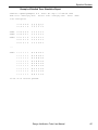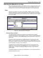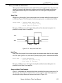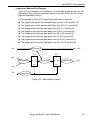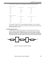
1
Design Verification Tools
User Manual
Version 8.0
Technical Support Line: 1- 800-LATTICE or (408) 428-6414
DE-VM Rev 8.0.1
Copyright
This document may not, in whole or part, be copied, photocopied, reproduced,
translated, or reduced to any electronic medium or machine-readable form without
prior written consent from Lattice Semiconductor Corporation.
The software described in this manual is copyrighted and all rights are reserved by
Lattice Semiconductor Corporation. Information in this document is subject to change
without notice.
The distribution and sale of this product is intended for the use of the original
purchaser only and for use only on the computer system specified. Lawful users of
this product are hereby licensed only to read the programs on the disks, cassettes, or
tapes from their medium into the memory of a computer solely for the purpose of
executing them. Unauthorized copying, duplicating, selling, or otherwise distributing
this product is a violation of the law.
Trademarks
The following trademarks are recognized by Lattice Semiconductor Corporation:
Generic Array Logic, ISP, ispANALYZER, ispATE, ispCODE, ispDCD,
ispDOWNLOAD, ispDS, ispDS+, ispEXPERT, ispGDS, ispGDX, ispHDL, ispJTAG,
ispSmartFlow, ispStarter, ispSTREAM, ispSVF, ispTA, ispTEST, ispTURBO,
ispVECTOR, ispVerilog, ispVHDL, ispVM, Latch-Lock, LHDL, pDS+, RFT, and Twin
GLB are trademarks of Lattice Semiconductor Corporation.
E2CMOS, GAL, ispGAL, ispLSI, pDS, pLSI, Silicon Forest, and UltraMOS are
registered trademarks of Lattice Semiconductor Corporation.
SPEEDSearch, Perfomance Analyst, and DesignDirect are trademarks of Vantis
Corporation. Kooldip, MACH, MACHPRO, MACHXL, Monolithic Memories, PAL,
PALASM, and Vantis are registered trademarks of Vantis Corporation.
Project Navigator is a trademark of Data I/O Corporation. ABEL-HDL is a registered
trademark of Data I/O Corporation.
Microsoft, Windows, and MS-DOS are registered trademarks of Microsoft
Corporation.
All other trademarks and registered trademarks are the property of their respective
owners.
Lattice Semiconductor Corporation
5555 NE Moore Ct.
Hillsboro, OR 97124
(503) 268-8000
December 1999
Design Verification Tools User Manual
2
Limited Warranty
Lattice Semiconductor Corporation warrants the original purchaser that the Lattice
Semiconductor software shall be free from defects in material and workmanship for a
period of ninety days from the date of purchase. If a defect covered by this limited
warranty occurs during this 90-day warranty period, Lattice Semiconductor will repair
or replace the component part at its option free of charge.
This limited warranty does not apply if the defects have been caused by negligence,
accident, unreasonable or unintended use, modification, or any causes not related to
defective materials or workmanship.
To receive service during the 90-day warranty period, contact Lattice Semiconductor
Corporation at:
Phone: 1-800-LATTICE
Fax: (408) 944-8450
E-mail: [email protected]
If the Lattice Semiconductor support personnel are unable to solve your problem over
the phone, we will provide you with instructions on returning your defective software
to us. The cost of returning the software to the Lattice Semiconductor Service Center
shall be paid by the purchaser.
Limitations on Warranty
Any applicable implied warranties, including warranties of merchantability and fitness
for a particular purpose, are hereby limited to ninety days from the date of purchase
and are subject to the conditions set forth herein. In no event shall Lattice
Semiconductor Corporation be liable for consequential or incidental damages
resulting from the breach of any expressed or implied warranties.
Purchaser’s sole remedy for any cause whatsoever, regardless of the form of action,
shall be limited to the price paid to Lattice Semiconductor for the Lattice
Semiconductor software.
The provisions of this limited warranty are valid in the United States only. Some states
do not allow limitations on how long an implied warranty lasts, or exclusion of
consequential or incidental damages, so the above limitation or exclusion may not
apply to you.
This warranty provides you with specific legal rights. You may have other rights which
vary from state to state.
Design Verification Tools User Manual
3
Table of Contents
Preface . . . . . . . . . . . . . . . . . . . . . . . . . . . . . . . . . . . . . . . . . . . . . . . . . . . . . . . . . . . . . . . . . . . . 9
What Is in this Manual . . . . . . . . . . . . . . . . . . . . . . . . . . . . . . . . . . . . . . . . . . . . . . . . . . . . . . .
Where to Look for Information . . . . . . . . . . . . . . . . . . . . . . . . . . . . . . . . . . . . . . . . . . . . . .
Documentation Conventions . . . . . . . . . . . . . . . . . . . . . . . . . . . . . . . . . . . . . . . . . . . . . . . . . .
Related Documentation . . . . . . . . . . . . . . . . . . . . . . . . . . . . . . . . . . . . . . . . . . . . . . . . . . . . . .
10
10
11
12
Chapter 1 Test Stimulus . . . . . . . . . . . . . . . . . . . . . . . . . . . . . . . . . . . . . . . . . . . . . . . . . . 13
Test Stimulus Overview . . . . . . . . . . . . . . . . . . . . . . . . . . . . . . . . . . . . . . . . . . . . . . . . . . . . . .
Creating a Test Vector File . . . . . . . . . . . . . . . . . . . . . . . . . . . . . . . . . . . . . . . . . . . . . . . . . . .
Test Vector Syntax . . . . . . . . . . . . . . . . . . . . . . . . . . . . . . . . . . . . . . . . . . . . . . . . . . . . . . .
TEST_VECTORS . . . . . . . . . . . . . . . . . . . . . . . . . . . . . . . . . . . . . . . . . . . . . . . . . . . . .
WAIT . . . . . . . . . . . . . . . . . . . . . . . . . . . . . . . . . . . . . . . . . . . . . . . . . . . . . . . . . . . . . . .
CYCLE . . . . . . . . . . . . . . . . . . . . . . . . . . . . . . . . . . . . . . . . . . . . . . . . . . . . . . . . . . . . .
Special Constants Support . . . . . . . . . . . . . . . . . . . . . . . . . . . . . . . . . . . . . . . . . . . . . . . . .
Using .P. to Preload Values in the State Diagram . . . . . . . . . . . . . . . . . . . . . . . . . . . .
Creating a Graphic Waveform File. . . . . . . . . . . . . . . . . . . . . . . . . . . . . . . . . . . . . . . . . . . . . .
Creating a VHDL Test Bench File . . . . . . . . . . . . . . . . . . . . . . . . . . . . . . . . . . . . . . . . . . . . . .
Manually Creating a VHDL Test Bench File . . . . . . . . . . . . . . . . . . . . . . . . . . . . . . . . . . . .
Creating a VHDL Test Bench File Using a VHDL Test Bench Template . . . . . . . . . . . . . .
Exporting a VHDL Test Bench File Using the Waveform Editor. . . . . . . . . . . . . . . . . . . . .
Creating a Verilog Test Fixture File . . . . . . . . . . . . . . . . . . . . . . . . . . . . . . . . . . . . . . . . . . . . .
Manually Creating a Verilog Test Fixture File. . . . . . . . . . . . . . . . . . . . . . . . . . . . . . . . . . .
Creating a Verilog Test Fixture File Using a Verilog Test Fixture Template. . . . . . . . . . . .
Exporting a Verilog Test Fixture File Using the Waveform Editor . . . . . . . . . . . . . . . . . . .
14
15
17
17
17
18
19
19
22
27
27
30
33
34
34
36
42
Chapter 2 Simulators . . . . . . . . . . . . . . . . . . . . . . . . . . . . . . . . . . . . . . . . . . . . . . . . . . . . . 43
Lattice Logic Simulator. . . . . . . . . . . . . . . . . . . . . . . . . . . . . . . . . . . . . . . . . . . . . . . . . . . . . . .
Simulation Overview. . . . . . . . . . . . . . . . . . . . . . . . . . . . . . . . . . . . . . . . . . . . . . . . . . . . . .
Functional Simulation . . . . . . . . . . . . . . . . . . . . . . . . . . . . . . . . . . . . . . . . . . . . . . . . . .
Timing Simulation . . . . . . . . . . . . . . . . . . . . . . . . . . . . . . . . . . . . . . . . . . . . . . . . . . . . .
Difference between Functional and Timing Simulation . . . . . . . . . . . . . . . . . . . . . . . . .
Running the Functional/Timing Simulation . . . . . . . . . . . . . . . . . . . . . . . . . . . . . . . . . . . . .
Running the Stand-alone Simulator . . . . . . . . . . . . . . . . . . . . . . . . . . . . . . . . . . . . . . . . . .
Comparing Functional Simulation Results with the Expected Values . . . . . . . . . . . . . . . .
Simulation Log . . . . . . . . . . . . . . . . . . . . . . . . . . . . . . . . . . . . . . . . . . . . . . . . . . . . . . .
Commands Used in the Simulator Control Panel . . . . . . . . . . . . . . . . . . . . . . . . . . . . . . . .
Equation Simulator. . . . . . . . . . . . . . . . . . . . . . . . . . . . . . . . . . . . . . . . . . . . . . . . . . . . . . . . . .
Equation Simulation Overview . . . . . . . . . . . . . . . . . . . . . . . . . . . . . . . . . . . . . . . . . . . . . .
Design Verification Tools User Manual
44
44
44
44
44
45
47
50
51
52
53
53
4
Equation Simulation Flow . . . . . . . . . . . . . . . . . . . . . . . . . . . . . . . . . . . . . . . . . . . . . . .
Invoking Equation Simulation . . . . . . . . . . . . . . . . . . . . . . . . . . . . . . . . . . . . . . . . . . . . . . .
Equation Simulator Model . . . . . . . . . . . . . . . . . . . . . . . . . . . . . . . . . . . . . . . . . . . . . . . . .
Controlling the Simulation Report. . . . . . . . . . . . . . . . . . . . . . . . . . . . . . . . . . . . . . . . . . . .
Using Break Points . . . . . . . . . . . . . . . . . . . . . . . . . . . . . . . . . . . . . . . . . . . . . . . . . . . .
Simulation Trace Levels . . . . . . . . . . . . . . . . . . . . . . . . . . . . . . . . . . . . . . . . . . . . . . . .
Simulation Output Formats . . . . . . . . . . . . . . . . . . . . . . . . . . . . . . . . . . . . . . . . . . . . . .
Simulating a JEDEC File . . . . . . . . . . . . . . . . . . . . . . . . . . . . . . . . . . . . . . . . . . . . . . . . . . . . .
53
55
56
57
57
58
61
67
Chapter 3 Waveform Viewer . . . . . . . . . . . . . . . . . . . . . . . . . . . . . . . . . . . . . . . . . . . . . . 68
Starting the Waveform Viewer . . . . . . . . . . . . . . . . . . . . . . . . . . . . . . . . . . . . . . . . . . . . . . . . .
Waveform Viewer Window . . . . . . . . . . . . . . . . . . . . . . . . . . . . . . . . . . . . . . . . . . . . . . . . .
Title Bar. . . . . . . . . . . . . . . . . . . . . . . . . . . . . . . . . . . . . . . . . . . . . . . . . . . . . . . . . . . . .
Waveform Name Area. . . . . . . . . . . . . . . . . . . . . . . . . . . . . . . . . . . . . . . . . . . . . . . . . .
Waveform Display Area . . . . . . . . . . . . . . . . . . . . . . . . . . . . . . . . . . . . . . . . . . . . . . . .
Prompt Line. . . . . . . . . . . . . . . . . . . . . . . . . . . . . . . . . . . . . . . . . . . . . . . . . . . . . . . . . .
Selecting the Waveforms to View . . . . . . . . . . . . . . . . . . . . . . . . . . . . . . . . . . . . . . . . . . . . . .
Show. . . . . . . . . . . . . . . . . . . . . . . . . . . . . . . . . . . . . . . . . . . . . . . . . . . . . . . . . . . . . . . . . .
Finding the Signal You Want. . . . . . . . . . . . . . . . . . . . . . . . . . . . . . . . . . . . . . . . . . . . .
Cross Probing with the Hierarchy Browser . . . . . . . . . . . . . . . . . . . . . . . . . . . . . . . . . .
Creating Multi-signal “Buses” . . . . . . . . . . . . . . . . . . . . . . . . . . . . . . . . . . . . . . . . . . . .
Duplicate. . . . . . . . . . . . . . . . . . . . . . . . . . . . . . . . . . . . . . . . . . . . . . . . . . . . . . . . . . . . . . .
Move. . . . . . . . . . . . . . . . . . . . . . . . . . . . . . . . . . . . . . . . . . . . . . . . . . . . . . . . . . . . . . . . . .
Hide . . . . . . . . . . . . . . . . . . . . . . . . . . . . . . . . . . . . . . . . . . . . . . . . . . . . . . . . . . . . . . . . . .
Selecting the Bus Radix . . . . . . . . . . . . . . . . . . . . . . . . . . . . . . . . . . . . . . . . . . . . . . . . . . .
Moving Around. . . . . . . . . . . . . . . . . . . . . . . . . . . . . . . . . . . . . . . . . . . . . . . . . . . . . . . . . . . . .
View Commands . . . . . . . . . . . . . . . . . . . . . . . . . . . . . . . . . . . . . . . . . . . . . . . . . . . . . . . .
Zoom In . . . . . . . . . . . . . . . . . . . . . . . . . . . . . . . . . . . . . . . . . . . . . . . . . . . . . . . . . . . . .
Zoom Out . . . . . . . . . . . . . . . . . . . . . . . . . . . . . . . . . . . . . . . . . . . . . . . . . . . . . . . . . . .
Pan . . . . . . . . . . . . . . . . . . . . . . . . . . . . . . . . . . . . . . . . . . . . . . . . . . . . . . . . . . . . . . . .
Full Fit . . . . . . . . . . . . . . . . . . . . . . . . . . . . . . . . . . . . . . . . . . . . . . . . . . . . . . . . . . . . . .
Scroll Bars. . . . . . . . . . . . . . . . . . . . . . . . . . . . . . . . . . . . . . . . . . . . . . . . . . . . . . . . . . .
Moving the Query Cursor . . . . . . . . . . . . . . . . . . . . . . . . . . . . . . . . . . . . . . . . . . . . . . . . . .
Tick Left, Tick Right. . . . . . . . . . . . . . . . . . . . . . . . . . . . . . . . . . . . . . . . . . . . . . . . . . . .
10 Left, 10 Right . . . . . . . . . . . . . . . . . . . . . . . . . . . . . . . . . . . . . . . . . . . . . . . . . . . . . .
Time=0, Time=End . . . . . . . . . . . . . . . . . . . . . . . . . . . . . . . . . . . . . . . . . . . . . . . . . . . .
To Marker . . . . . . . . . . . . . . . . . . . . . . . . . . . . . . . . . . . . . . . . . . . . . . . . . . . . . . . . . . .
To Time . . . . . . . . . . . . . . . . . . . . . . . . . . . . . . . . . . . . . . . . . . . . . . . . . . . . . . . . . . . . .
Next Change . . . . . . . . . . . . . . . . . . . . . . . . . . . . . . . . . . . . . . . . . . . . . . . . . . . . . . . . .
Next Trigger . . . . . . . . . . . . . . . . . . . . . . . . . . . . . . . . . . . . . . . . . . . . . . . . . . . . . . . . .
Jumping to Events . . . . . . . . . . . . . . . . . . . . . . . . . . . . . . . . . . . . . . . . . . . . . . . . . . . . . . .
Triggers . . . . . . . . . . . . . . . . . . . . . . . . . . . . . . . . . . . . . . . . . . . . . . . . . . . . . . . . . . . . . . .
Analysis Techniques . . . . . . . . . . . . . . . . . . . . . . . . . . . . . . . . . . . . . . . . . . . . . . . . . . . . . . . .
Logic Level and Time Measurements. . . . . . . . . . . . . . . . . . . . . . . . . . . . . . . . . . . . . . . . .
Interaction with the Hierarchy Navigator. . . . . . . . . . . . . . . . . . . . . . . . . . . . . . . . . . . . . . .
Displaying Simulation Values on a Schematic . . . . . . . . . . . . . . . . . . . . . . . . . . . . . . . . . .
View Report . . . . . . . . . . . . . . . . . . . . . . . . . . . . . . . . . . . . . . . . . . . . . . . . . . . . . . . . . . . .
Saving and Printing Waveforms. . . . . . . . . . . . . . . . . . . . . . . . . . . . . . . . . . . . . . . . . . . . . . . .
Design Verification Tools User Manual
69
69
69
69
69
70
71
71
71
72
72
72
72
72
72
73
73
73
73
73
73
73
74
74
74
74
74
74
74
74
75
75
76
76
76
77
77
78
5
Saving Waveforms . . . . . . . . . . . . . . . . . . . . . . . . . . . . . . . . . . . . . . . . . . . . . . . . . . . . . . .
Printing Waveforms . . . . . . . . . . . . . . . . . . . . . . . . . . . . . . . . . . . . . . . . . . . . . . . . . . . . . .
Start Time . . . . . . . . . . . . . . . . . . . . . . . . . . . . . . . . . . . . . . . . . . . . . . . . . . . . . . . . . . .
End Time. . . . . . . . . . . . . . . . . . . . . . . . . . . . . . . . . . . . . . . . . . . . . . . . . . . . . . . . . . . .
Time Scale . . . . . . . . . . . . . . . . . . . . . . . . . . . . . . . . . . . . . . . . . . . . . . . . . . . . . . . . . .
Number of Pages . . . . . . . . . . . . . . . . . . . . . . . . . . . . . . . . . . . . . . . . . . . . . . . . . . . . .
Width of Names. . . . . . . . . . . . . . . . . . . . . . . . . . . . . . . . . . . . . . . . . . . . . . . . . . . . . . .
Print Names On All Pages . . . . . . . . . . . . . . . . . . . . . . . . . . . . . . . . . . . . . . . . . . . . . .
Print. . . . . . . . . . . . . . . . . . . . . . . . . . . . . . . . . . . . . . . . . . . . . . . . . . . . . . . . . . . . . . . .
78
78
78
78
78
78
79
79
79
Chapter 4 Waveform Editor . . . . . . . . . . . . . . . . . . . . . . . . . . . . . . . . . . . . . . . . . . . . . . . 80
Running the Waveform Editor . . . . . . . . . . . . . . . . . . . . . . . . . . . . . . . . . . . . . . . . . . . . . . . . .
Running the Waveform Editor from the Project Navigator . . . . . . . . . . . . . . . . . . . . . . . . .
Running the Waveform Editor from the Simulator Control Panel . . . . . . . . . . . . . . . . . . . .
Creating Waveform Stimulus . . . . . . . . . . . . . . . . . . . . . . . . . . . . . . . . . . . . . . . . . . . . . . . . . .
Displaying the Signal Names . . . . . . . . . . . . . . . . . . . . . . . . . . . . . . . . . . . . . . . . . . . . . . . . . .
Adding New Waveform Names . . . . . . . . . . . . . . . . . . . . . . . . . . . . . . . . . . . . . . . . . . . . .
Adding Test Points . . . . . . . . . . . . . . . . . . . . . . . . . . . . . . . . . . . . . . . . . . . . . . . . . . . . . . .
Using Test Points . . . . . . . . . . . . . . . . . . . . . . . . . . . . . . . . . . . . . . . . . . . . . . . . . . . . .
Importing Signal Names . . . . . . . . . . . . . . . . . . . . . . . . . . . . . . . . . . . . . . . . . . . . . . . . . . .
Selecting Signal Names to Display. . . . . . . . . . . . . . . . . . . . . . . . . . . . . . . . . . . . . . . . . . .
Hiding and Restoring Waveforms. . . . . . . . . . . . . . . . . . . . . . . . . . . . . . . . . . . . . . . . . . . .
Drawing the Waveforms. . . . . . . . . . . . . . . . . . . . . . . . . . . . . . . . . . . . . . . . . . . . . . . . . . . . . .
Edit and Query Modes . . . . . . . . . . . . . . . . . . . . . . . . . . . . . . . . . . . . . . . . . . . . . . . . . . . .
Simulation Timing Values . . . . . . . . . . . . . . . . . . . . . . . . . . . . . . . . . . . . . . . . . . . . . . . . . .
Creating Waveforms. . . . . . . . . . . . . . . . . . . . . . . . . . . . . . . . . . . . . . . . . . . . . . . . . . . . . .
Editing Waveforms . . . . . . . . . . . . . . . . . . . . . . . . . . . . . . . . . . . . . . . . . . . . . . . . . . . . . . .
Setting State and Duration . . . . . . . . . . . . . . . . . . . . . . . . . . . . . . . . . . . . . . . . . . . . . .
Selecting Pulses . . . . . . . . . . . . . . . . . . . . . . . . . . . . . . . . . . . . . . . . . . . . . . . . . . . . . .
Adding Pulses . . . . . . . . . . . . . . . . . . . . . . . . . . . . . . . . . . . . . . . . . . . . . . . . . . . . . . . .
Selecting Spans . . . . . . . . . . . . . . . . . . . . . . . . . . . . . . . . . . . . . . . . . . . . . . . . . . . . . .
Graphically Changing the Length of a Pulse. . . . . . . . . . . . . . . . . . . . . . . . . . . . . . . . .
Changing the Offset of a Waveform . . . . . . . . . . . . . . . . . . . . . . . . . . . . . . . . . . . . . . .
Creating and Using Patterns . . . . . . . . . . . . . . . . . . . . . . . . . . . . . . . . . . . . . . . . . . . . . . .
Creating Patterns . . . . . . . . . . . . . . . . . . . . . . . . . . . . . . . . . . . . . . . . . . . . . . . . . . . . .
Inserting Patterns . . . . . . . . . . . . . . . . . . . . . . . . . . . . . . . . . . . . . . . . . . . . . . . . . . . . .
Hierarchical Patterns. . . . . . . . . . . . . . . . . . . . . . . . . . . . . . . . . . . . . . . . . . . . . . . . . . .
Editing Patterns. . . . . . . . . . . . . . . . . . . . . . . . . . . . . . . . . . . . . . . . . . . . . . . . . . . . . . .
Scaling Patterns and Waveforms . . . . . . . . . . . . . . . . . . . . . . . . . . . . . . . . . . . . . . . . .
Repeating Patterns and Waveforms . . . . . . . . . . . . . . . . . . . . . . . . . . . . . . . . . . . . . . .
Deleting, Cutting, Copying, and Pasting Waveforms . . . . . . . . . . . . . . . . . . . . . . . . . . . . .
Saving Changes . . . . . . . . . . . . . . . . . . . . . . . . . . . . . . . . . . . . . . . . . . . . . . . . . . . . . . . . .
Exporting the Stimulus File . . . . . . . . . . . . . . . . . . . . . . . . . . . . . . . . . . . . . . . . . . . . . . . . . . .
Using the Export Command . . . . . . . . . . . . . . . . . . . . . . . . . . . . . . . . . . . . . . . . . . . . . . . .
Changing the Waveforms for Exporting . . . . . . . . . . . . . . . . . . . . . . . . . . . . . . . . . . . . . . .
Selecting Nodes . . . . . . . . . . . . . . . . . . . . . . . . . . . . . . . . . . . . . . . . . . . . . . . . . . . . . .
Changing Polarity . . . . . . . . . . . . . . . . . . . . . . . . . . . . . . . . . . . . . . . . . . . . . . . . . . . . .
Changing Offset . . . . . . . . . . . . . . . . . . . . . . . . . . . . . . . . . . . . . . . . . . . . . . . . . . . . . .
Design Verification Tools User Manual
81
81
81
82
83
83
84
84
84
86
87
89
89
89
89
90
90
91
91
92
92
93
93
93
94
95
95
95
96
97
97
98
98
98
99
99
99
6
Waveform Editor Configuration . . . . . . . . . . . . . . . . . . . . . . . . . . . . . . . . . . . . . . . . . . . . . . .
Timing Options . . . . . . . . . . . . . . . . . . . . . . . . . . . . . . . . . . . . . . . . . . . . . . . . . . . . . . . . .
Time Units . . . . . . . . . . . . . . . . . . . . . . . . . . . . . . . . . . . . . . . . . . . . . . . . . . . . . . . . . .
Display Options . . . . . . . . . . . . . . . . . . . . . . . . . . . . . . . . . . . . . . . . . . . . . . . . . . . . . . . .
100
100
100
100
Chapter 5 Timing Analyzers . . . . . . . . . . . . . . . . . . . . . . . . . . . . . . . . . . . . . . . . . . . . . 102
Performance Analyst . . . . . . . . . . . . . . . . . . . . . . . . . . . . . . . . . . . . . . . . . . . . . . . . . . . . . . .
Overview. . . . . . . . . . . . . . . . . . . . . . . . . . . . . . . . . . . . . . . . . . . . . . . . . . . . . . . . . . . . . .
Timing Model. . . . . . . . . . . . . . . . . . . . . . . . . . . . . . . . . . . . . . . . . . . . . . . . . . . . . . . .
Analysis Types . . . . . . . . . . . . . . . . . . . . . . . . . . . . . . . . . . . . . . . . . . . . . . . . . . . . . . . . .
fMAX . . . . . . . . . . . . . . . . . . . . . . . . . . . . . . . . . . . . . . . . . . . . . . . . . . . . . . . . . . . . . .
tSU . . . . . . . . . . . . . . . . . . . . . . . . . . . . . . . . . . . . . . . . . . . . . . . . . . . . . . . . . . . . . . .
tPD . . . . . . . . . . . . . . . . . . . . . . . . . . . . . . . . . . . . . . . . . . . . . . . . . . . . . . . . . . . . . . .
tCO . . . . . . . . . . . . . . . . . . . . . . . . . . . . . . . . . . . . . . . . . . . . . . . . . . . . . . . . . . . . . . .
tOE . . . . . . . . . . . . . . . . . . . . . . . . . . . . . . . . . . . . . . . . . . . . . . . . . . . . . . . . . . . . . . .
tCOE . . . . . . . . . . . . . . . . . . . . . . . . . . . . . . . . . . . . . . . . . . . . . . . . . . . . . . . . . . . . . .
Path Tracing Rules . . . . . . . . . . . . . . . . . . . . . . . . . . . . . . . . . . . . . . . . . . . . . . . . . . . . . .
Tracing Enabled through Bidirectional Paths . . . . . . . . . . . . . . . . . . . . . . . . . . . . . . .
Tracing Enabled through Register Asynch S/R Inputs . . . . . . . . . . . . . . . . . . . . . . . .
Tracing Enabled through Transparent Latch D Inputs . . . . . . . . . . . . . . . . . . . . . . . .
Tracing Enabled through Ripple Clocks . . . . . . . . . . . . . . . . . . . . . . . . . . . . . . . . . . .
Running Static Timing Analysis . . . . . . . . . . . . . . . . . . . . . . . . . . . . . . . . . . . . . . . . . . . .
Comparing the Timing Results of Different Fitter Options. . . . . . . . . . . . . . . . . . . . . .
Comparing the Results of Different Timing Options . . . . . . . . . . . . . . . . . . . . . . . . . .
Running Timing Analysis in Batch Mode . . . . . . . . . . . . . . . . . . . . . . . . . . . . . . . . . . . . .
Batch Commands . . . . . . . . . . . . . . . . . . . . . . . . . . . . . . . . . . . . . . . . . . . . . . . . . . . .
Using the Batch Timer. . . . . . . . . . . . . . . . . . . . . . . . . . . . . . . . . . . . . . . . . . . . . . . . .
Batch File Examples . . . . . . . . . . . . . . . . . . . . . . . . . . . . . . . . . . . . . . . . . . . . . . . . . .
ispEXPERT Timing Analyzer . . . . . . . . . . . . . . . . . . . . . . . . . . . . . . . . . . . . . . . . . . . . . . . . .
Overview. . . . . . . . . . . . . . . . . . . . . . . . . . . . . . . . . . . . . . . . . . . . . . . . . . . . . . . . . . . . . .
Path Analysis . . . . . . . . . . . . . . . . . . . . . . . . . . . . . . . . . . . . . . . . . . . . . . . . . . . . . . .
Frequency Calculation . . . . . . . . . . . . . . . . . . . . . . . . . . . . . . . . . . . . . . . . . . . . . . . .
Setup and Hold Time Evaluation. . . . . . . . . . . . . . . . . . . . . . . . . . . . . . . . . . . . . . . . .
Tpd Calculation . . . . . . . . . . . . . . . . . . . . . . . . . . . . . . . . . . . . . . . . . . . . . . . . . . . . . .
Tco Calculation . . . . . . . . . . . . . . . . . . . . . . . . . . . . . . . . . . . . . . . . . . . . . . . . . . . . . .
Path Enumeration . . . . . . . . . . . . . . . . . . . . . . . . . . . . . . . . . . . . . . . . . . . . . . . . . . . .
GLB Boundary Calculation . . . . . . . . . . . . . . . . . . . . . . . . . . . . . . . . . . . . . . . . . . . . .
Running the Timing Analyzer . . . . . . . . . . . . . . . . . . . . . . . . . . . . . . . . . . . . . . . . . . . . . .
Timing Analyzer Report Files . . . . . . . . . . . . . . . . . . . . . . . . . . . . . . . . . . . . . . . . . . . . . .
Timing Explorer . . . . . . . . . . . . . . . . . . . . . . . . . . . . . . . . . . . . . . . . . . . . . . . . . . . . . . . .
Signal Navigator . . . . . . . . . . . . . . . . . . . . . . . . . . . . . . . . . . . . . . . . . . . . . . . . . . . . .
Pop-up Menus from the Signal Navigator . . . . . . . . . . . . . . . . . . . . . . . . . . . . . . . . . .
Timing Explorer Tables . . . . . . . . . . . . . . . . . . . . . . . . . . . . . . . . . . . . . . . . . . . . . . . .
Pop-Up Menus from the Timing Tables . . . . . . . . . . . . . . . . . . . . . . . . . . . . . . . . . . .
Timing Path Report . . . . . . . . . . . . . . . . . . . . . . . . . . . . . . . . . . . . . . . . . . . . . . . . . . .
Running the Timing Analyzer from the Command Line . . . . . . . . . . . . . . . . . . . . . . . . . .
Design Verification Tools User Manual
103
103
103
104
104
105
106
107
108
108
109
109
109
110
110
111
114
114
115
115
116
117
120
120
120
121
123
125
125
126
128
129
131
133
133
134
135
137
138
139
7
Chapter 6 ModelSim Simulator . . . . . . . . . . . . . . . . . . . . . . . . . . . . . . . . . . . . . . . . . . 140
Running the ispDesignExpert ModelSim Simulator . . . . . . . . . . . . . . . . . . . . . . . . . . . . . . . .
Using Compiled Lattice/Vantis Libraries. . . . . . . . . . . . . . . . . . . . . . . . . . . . . . . . . . . . . .
Simulating VHDL and Verilog HDL Designs. . . . . . . . . . . . . . . . . . . . . . . . . . . . . . . . . . .
XRESET and XTEST_OE Handling for Post-route Simulation. . . . . . . . . . . . . . . . . . . . .
Manually Simulating a Design . . . . . . . . . . . . . . . . . . . . . . . . . . . . . . . . . . . . . . . . . . . . .
Running the Stand-alone ModelSim Simulator . . . . . . . . . . . . . . . . . . . . . . . . . . . . . . . . . . .
Compiling Lattice/Vantis Libraries for ModelSim 5.2 . . . . . . . . . . . . . . . . . . . . . . . . . . . . . . .
Design Verification Tools User Manual
141
141
142
143
144
145
148
8
Preface
This manual describes a variety of tools for verifying logic designs in ispDesignExpert
from the Lattice Semiconductor Corporation (LSC). It serves as a primary learning
guide for creating test stimulus, implementing simulation, viewing the simulation
results, querying timing information, and running the third-party simulator for VHDL
and Verilog HDL simulation.
Design Verification Tools User Manual
9
What Is in this Manual
What Is in this Manual
This user manual contains the information on the following topics:
■
■
■
■
■
■
■
■
■
■
Creating test stimulus
Running the Lattice Logic Simulator for ispLSI/GAL designs
Functional/Timing simulation
Running the Equation Simulator for MACH/PAL designs
Simulating JEDEC files for GAL/PAL designs
Using the Waveform Viewer to view the simulation results
Using the Waveform Editing Tool to create waveforms
Running the Performance Analyst for MACH design timing analysis
Running the ispEXPERT Timing Analyzer for ispLSI design timing analysis
Using ModelSim to do VHDL and Verilog HDL simulation
Where to Look for Information
Chapter 1, Test Stimulus – Gives an overview of test stimulus. Describes 4 types of
stimulus files and how they are created in ispDesignExpert.
Chapter 2, Simulators – Describes how to run the Lattice Logic Simulator for
ispLSI/GAL designs and run the Equation Simulator for MACH/PAL designs. Also
discusses running JEDEC simulation for GAL/PAL designs.
Chapter 3, Waveform Viewer – Shows how to add signals to the display of the
Waveform Viewer.
Chapter 4, Waveform Editor – Shows how to create and edit waveforms using the
commands from the Waveform Editor.
Chapter 5, Timing Analyzers – Discusses two types of timing analyzers for postroute design verification: the Performance Analyst for MACH designs, and the
ispEXPERT Timing Analyzer for ispLSI designs.
Chapter 6, ModelSim Simulator – Explains how to simulate VHDL and Verilog HDL
designs with the ispDesignExpert ModelSim Simulator. Also explains how to run the
stand-alone ModelSim Simulator.
Design Verification Tools User Manual
10
Documentation Conventions
Documentation Conventions
This user manual follows the typographic conventions listed here:
Convention
Definition and Usage
Italics
Italicized text represents variable input. For example:
design.1
This means you must replace design with the file name you used for all the files
relevant to your design.
Valuable information may be italicized for emphasis. Book titles also appear in
italics.
The beginning of a procedure appears in italics. For example:
To run the functional simulator:
Bold
Valuable information may be boldfaced for emphasis. Commands are shown in
boldface. For example:
Select File ⇒ Open from the Waveform Viewer.
Courier
Font
Monospaced (Courier) font indicates file and directory names and text that the
system displays. For example:
The C:\ispsys\CONFIG subdirectory contains...
Bold
Courier
Bold Courier font indicates text you type in response to system prompts. For
example:
SET YBUS [Y0..Y6];
|...|
Vertical bars indicate options that are mutually exclusive; you can select only one.
For example:
INPUT|OUTPUT|BIDI
“Quotes”
Titles of chapters or sections in chapters in this manual are shown in quotation
marks. For example:
See Chapter 1, “Introduction.”
✍ NOTE
Indicates a special note.
▲ CAUTION
Indicates a situation that could cause loss of data or other problems.
❖ TIP
Indicates a special hint that makes using the software easier.
⇒
Indicates a menu option leading to a submenu option. For example:
File ⇒ New
Design Verification Tools User Manual
11
Related Documentation
Related Documentation
In addition to this manual, you might find the following reference material helpful:
■
■
■
■
■
■
■
■
■
■
ispDesignExpert User Manual
ispDesignExpert Getting Started Manual
ABEL Design Manual
ABEL-HDL Reference Manual
Schematic Entry User Manual
ispLSI Macro Library Reference Manual
5K/8K Macro Library Supplement
ispEXPERT Compiler User Manual
ISP Daisy Chain Download User Manual
VHDL and Verilog Simulation User Manual
These books provide technical specifications for the Lattice/Vantis device families
and give helpful information on device use and design development.
Design Verification Tools User Manual
12
Chapter 1
Test Stimulus
This chapter gives an introduction on creating stimulus files for input to the simulator.
It covers the following topics:
■
■
■
■
Creating a test vector file
Creating a graphic waveform file
Creating a VHDL test bench file
Creating a Verilog test fixture file
Design Verification Tools User Manual
13
Test Stimulus Overview
Test Stimulus Overview
Once you have completed your design (or a module of the design), you may test it to
confirm that it behaves the way you expect it to. Simulation requires a test stimulus
file that specifies the input waveforms. There are four types of test stimulus that can
be accessed from the Sources window of the Project Navigator:
■
■
■
■
Test vector file (.abv)
Graphic waveform file (.wdl)
VHDL test bench file (.vhd)
Verilog test fixture file (.tf)
The Lattice Logic Simulator uses .abv and .wdl files to simulate the design, the
Equation Simulator also accepts .abv (or -vectors) files as the stimulus; while you
need to use .vhd and .tf files as the stimulus for the ModelSim Simulator to
perform VHDL/Verilog HDL simulation.
Design Verification Tools User Manual
14
Creating a Test Vector File
Creating a Test Vector File
Test vectors can be specified in two ways:
■
■
Specified in an ABEL-HDL source
The most common method is to place test vectors in an ABEL-HDL source file. If
you use this method, the Project Navigator will detect the presence of test vectors
in the source file and create a “dummy” test vector file. This file indicates to the
system that the actual test vectors are in the ABEL-HDL source file.
Specified in an external Test Vector file (.abv).
Placing test vectors in an ABV file instead of in an ABEL-HDL source file improves
processing time. By placing test vectors in an ABV file, you will be able to change
the test vectors and resimulate without having to recompile the logic.
The following section explains how to create a .abv file.
To create a .abv file:
1. Select the Source ⇒ New menu item from the ispDesignExpert Project Navigator.
The New Source dialog box appears, prompting you to choose the type for the
new source in your project (Figure 1-1).
Figure 1-1. New Source Dialog Box
2. Click on ABEL Test Vectors in the New field and then click OK. The Text Editor is
launched, along with the New File dialog box (Figure 1-2), prompting you for the
new file name.
Design Verification Tools User Manual
15
Creating a Test Vector File
Figure 1-2. New File Dialog box
3. Enter the name for the .abv file in the File Name field, then click OK. The Text
Editor is displayed.
4. Type the syntax for the test vectors in the Text Editor. The keywords and
comments are color-coded. Figure 1-3 shows a sample test vector file.
Figure 1-3. Sample Test Vector File
✍ NOTE
The module name in a .abv file must be the same as the
name of the top level module.
5. Select the File ⇒ Save menu item to save the changes.
Design Verification Tools User Manual
16
Creating a Test Vector File
Test Vector Syntax
The keywords that are supported in an ABEL test vector file are described in this
section.
TEST_VECTORS
Test vectors specify the expected functional operation of a logic device by explicitly
defining the device outputs as functions of the inputs. Test vectors are used for
simulation of an internal model of the device and for functional testing of the
programmed device. The syntax is:
TEST_VECTORS [note]
(inputs -> outputs)
[cycle-clause]
[wait-clause]
invalues -> outvalues;
Example
TEST_VECTORS
( [A,B] -> [C,D] )
CYCLE clk (0,100) (1,100);
0 -> 3;
WAIT 100; 1 -> 2;
WAIT 100; 2 -> 1;
WAIT 100; 3 -> 0;
✍ NOTE
After simulation by the Lattice Logic Simulator, the input and
output signals specified in the TEST_VECTORS section will
be automatically displayed in the Waveform Viewer and in the
trace report which can be accessed from View ⇒ Trace
Report in the Simulator Control Panel.
WAIT
This keyword represents the relative time delay which effects the test vectors
immediately following the WAIT statement. It can be used in the MACRO block only
when MACRO is used in the TEST_VECTORS block. The default time unit is
nano-second. The syntax for WAIT is:
WAIT <integer>;
Design Verification Tools User Manual
17
Creating a Test Vector File
Example
test_vectors MACRO {
WAIT 10;
1 -> [0,1];
WAIT 24;
6 -> [0,1];
WAIT 34;
8 -> [1.0];
};
CYCLE
This keyword specifies the signal to repeat until the end of simulation. The default
time unit is nano-second. The syntax for CYCLE is:
CYCLE signal_name (logic_value, integer) (logic_value,
integer) [(logic_value, integer)];
Example
CYCLE clk1 (0,3) (1,5);
✍ NOTE
The keywords WAIT and CYCLE are only defined in the Lattice
Logic Simulator. They cannot be used with all of the supported
special constants, except .R.. See “Special Constants
Support” on the following page for information.
Design Verification Tools User Manual
18
Creating a Test Vector File
Special Constants Support
The following constants are supported:
■
■
■
■
■
■
■
■
.C. – Translates to 0, 1, 0 and time unit delay is 3
.K. – Translates to 1, 0, 1 and time unit delay is 3
.D. – Translates to 1, 0 and time unit delay is 2
.U. – Translates to 0, 1 and time unit delay is 2
.F. – Translates to .Z.
.SV#. – #2 - 9 translate to 0 (can be changed in a .ini file)
.P. – Assigns the value provided in vectors to signals. When .C., .K., .U., and .D.
appear as .P. does, they are translated to ‘0’
The .P. in a .abv file means supervoltage preload. It is used to load registers to
the desired state. If the registers do not set the preload value when CLK is set to
.P., the simulation result is complex and unpredictable.
.P. is only effective when used as the .clk of a flip-flop. If it is not used as .clk, it
is translated to ‘0’.
.R. – Specifies random test vector values in test vector blocks. Translates to 0 or 1
randomly.
Using .P. to Preload Values in the State Diagram
.P. is a special constant used to preload values to registers. Its main function is to
preload invalid values to test the function of a design, especially for an invalid state of
the state machine. The following is an example to show the usage of .P..
MODULE preload;
TITLE ’Using Special Constant .P. to show state transition’
"Inputs
clk
pin;
reset
pin;
"Outputs
[q0..q2]
pin istype ’reg’;
"State Register
sreg = [q2..q0];
Design Verification Tools User Manual
19
Creating a Test Vector File
"State
A = [0,
B = [0,
C = [0,
D = [0,
E = [1,
0,
0,
1,
1,
0,
0];
1];
0];
1];
0];
"Illegal states
F = [1, 0, 1];
G = [1, 1, 0];
H = [1, 1, 1];
Equations
sreg.clk = clk;
sreg.re = reset;
State_diagram sreg;
State A: goto B;
State B: goto C;
State C: goto D;
State D: goto E;
State E: goto A;
"Illegal state
State F: goto A;
State G: goto A;
State H: goto A;
"Nomal
Test_vectors ([reset, clk] -> sreg);
[1,
0 ] -> 0;
@repeat 8 {
[0, .c.]-> .x.;};
Design Verification Tools User Manual
20
Creating a Test Vector File
"Preload to test invalid state
Test_vectors([reset, clk, [sreg]] -> sreg)
[1, 0, [.x.]] -> 0;
[0, .P., [ F ]] -> F;
[0, 0, [.x.]] -> .x.;
[0, .c., [.x.]] -> A;
[0, .P., [ G ]] -> G;
[0, 0, [.x.]] -> .x.;
[0, .c., [.x.]] -> A;
[0, .P., [ H ]] -> H;
[0, 0, [.x.]] -> .x.;
[0, .c., [.x.]] -> A;
END;
Design Verification Tools User Manual
21
Creating a Graphic Waveform File
Creating a Graphic Waveform File
The Waveform Editor uses a data model called the Waveform Description Language
(WDL). The language represents a waveform as a sequence of signal states
separated by time intervals. The language also has constructs that let you express
the waveform pattern hierarchically. (You do not have to be familiar with the Waveform
Description Language to use the Waveform Editor.)
The following sections describe how to create a WDL file with the Waveform Editing
Tool.
To create a .wdl file:
1. Select the Source ⇒ New menu item from the Project Navigator. The New
Source dialog box appears, prompting you to choose the type of the new source in
your project (Figure 1-4).
Figure 1-4. New Source Dialog Box
2. Click on Waveform Stimulus in the New field and then click OK. The Associate
Waveform Stimulus dialog box (Figure 1-5) appears, prompting you to associate
the new waveform stimulus file with the selected device or one of your design
modules.
Figure 1-5. Associate Waveform Stimulus Dialog Box
Design Verification Tools User Manual
22
Creating a Graphic Waveform File
✍ NOTE
If you associate the waveform stimulus file with the selected
device in your project, both functional and timing simulation
processes are supported. However, if you associate the
waveform stimulus file with a design module, only functional
simulation is available.
3. Select the source with which you want to associate the .wdl file, then click OK.
The Waveform Editing Tool appears with the New Waveform Stimulus dialog box
(Figure 1-6).
Figure 1-6. New Waveform Stimulus Dialog Box
4. Enter the name in the WDL File Name field, and click OK. The Waveform Editing
Tool is displayed with the file name on the title bar.
At this stage, the Waveform Editor creates two files, project.wet and
project.wdl. The .wet file contains the names of the nodes or signals you
create waveforms for. The .wdl file contains the waveforms themselves, in WDL
format. You can use the Save As command to save files under a different base
name to create multiple stimulus files for a single project.
5. Select the Edit ⇒ New Wave menu item, and the Add New Wave dialog box
displays (Figure 1-7).
Design Verification Tools User Manual
23
Creating a Graphic Waveform File
Figure 1-7. Add New Wave Dialog Box
6. Specify a signal name or a bus name and select the polarity for it, then click the
Add button to add the name to the display.
In the display, a letter next to the name indicates its type: I for input, B for
bidirectional pin, O for output, T for test point, G for global signal, and P for
pattern.
Or
You can import signal names directly from a .naf file using the
Edit ⇒ Import Wave command. In the pop-up Import dialog box, click the
Browse button to select a desired .naf file. All the signal names in the selected
.naf file will be displayed in the left field (Figure 1-8). Deselect any of the Input,
Output, Bidir, Global, and Test Pt fields to narrow the signals accordingly to your
needs. Select the signals you need for the new WDL file using relevant buttons:
• Add – Adds the selected signal(s) from the left field to the right field.
• Delete – Deletes the selected signal(s) from the right field.
• Add All – Adds all the signals from the left field to the right field.
• Clear – Removes all the signals from the right field.
• Cancel – Cancels the import operation.
• Show – Adds all the signals in the right field to the Waveform Editing Tool
window.
Design Verification Tools User Manual
24
Creating a Graphic Waveform File
Figure 1-8. Import Dialog Box
✍
NOTE
If you cannot find a desired .naf file, open the corresponding
source in the Text Editor (if it is an HDL source) or the
Schematic Editor (if it is a schematic source). Make a
modification to that source, which will not change its original
functionality. For example, add a space at the end of an HDL
file, or add a wire to a schematic file and then remove the wire.
Save the modified source file. Then you will be able to find the
relevant .naf file.
Or
If you have a schematic source in your project, use the Copy Externals command
to list the signal names to choose for the new waveform. Open the .sch file in the
Hierarchy Navigator. Select File ⇒ Copy Externals in the Waveform Editing Tool.
Select the Edit ⇒ Show command. The Show Patterns dialog box appears with
the signal names of the schematic source listed in the Patterns field (Figure 1-9).
Choose the desired signal and click Show. The signal name will be displayed in
the Waveform Editing Tool.
Design Verification Tools User Manual
25
Creating a Graphic Waveform File
Figure 1-9. Show Patterns Dialog Box
7. In the Waveform Editing Tool window, click on the name you want to create a
waveform for. The name is highlighted with light gray diagonal lines.
8. Move the mouse to the waveform section of the window and click where you want
the first Transition. (You must click in the area next to the highlighted name.) A line
is drawn to show the first section (called a Pulse) of the waveform.
9. Click again to create the second Transition. The second Pulse that is drawn has
the opposite state of the first Pulse. Continue clicking to complete the waveform.
10. The Selected Bit Pulse dialog box (Figure 1-10) gives you complete control over
the state and duration of each Pulse. Select the state in the States list box for the
signal, and specify the duration in the Duration text box.
Figure 1-10. Selected Bit Pulse Dialog Box
11. Select File ⇒ Save from the Waveform Editing Tool to save the changes.
Refer to Chapter 4, “Waveform Editor” for detailed information on creating
waveforms with the Waveform Editing Tool.
Design Verification Tools User Manual
26
Creating a VHDL Test Bench File
Creating a VHDL Test Bench File
Before you do VHDL simulation, you need to create a test bench file as the test
stimulus that specifies the input for simulation.
You can manually create a VHDL test bench file (*.vhd), use a VHDL test bench
template file (*.vht), or export a VHDL test bench file with the Waveform Editor.
Manually Creating a VHDL Test Bench File
To manually create a VHDL test bench file:
1. Select the Source ⇒ New menu item from the Project Navigator. The New
Source dialog box appears, prompting you to choose the type of the new source in
your project (Figure 1-11).
Figure 1-11. New Source Dialog Box
2. Select VHDL Test Bench in the New field and then click OK. The Associate VHDL
Test Bench dialog box (Figure 1-12) appears, prompting you to associate the new
VHDL test bench file with the selected device or one of your design modules.
Figure 1-12. Associate VHDL Test Bench Dialog Box
✍ NOTE
If you associate the VHDL test bench file with the selected
device in your project, both VHDL functional simulation and
VHDL post-route simulation processes are supported.
However, if you associate the test bench file with a design
module, only VHDL functional simulation is available.
Design Verification Tools User Manual
27
Creating a VHDL Test Bench File
3. Select the source with which you want to associate the .vhd file, click OK. The
Text Editor appears with the New File dialog box (Figure 1-13).
Figure 1-13. New VHDL Test Bench File Dialog Box
4. Enter a name for the .vhd file in the File Name field and click OK. The Text Editor
is displayed with the new file name on the title bar. The new VHDL test bench file
will appear in the Source window of the Project Navigator.
5. Use the items in the Edit menu of the Text Editor to cut, copy, paste, find, or
replace text. You can simply paste the VHDL test bench template (*.vht) into
your new test bench file and save it as a .vhd file.
You should follow two important rules when creating the test bench file:
• the entity name of the test bench is the same as the file name of the test
bench;
• the instance name of the top design module is UUT.
6. If your design uses Lattice macros, you should include Lattice libraries or generic
library into your VHDL test bench file.
• To include Lattice libraries, you should add the following lines into the VHDL
test bench file:
For ispLSI 1000, 2000, 3000, 5000, and 8000 device families:
library lat_vhd;
use lat_vhd.components.all;
For ispLSI 6000 device family:
library lsc_mod;
use lsc_mod.componets.all;
Design Verification Tools User Manual
28
Creating a VHDL Test Bench File
• To include generic library, you should add the following lines into the VHDL test
bench file:
library generics;
use generics.components.all;
✍ NOTE
In order to keep backward compatible, ispDesignExpert allows
library lattice to have the same effect as library
lat_vhd.
To run the simulation smoothly, you need to be familiar with the structure of Lattice
simulation libraries first. Refer to Chapter 6, “ModelSim Simulator” for more
information.
Design Verification Tools User Manual
29
Creating a VHDL Test Bench File
Creating a VHDL Test Bench File Using a VHDL Test Bench Template
To create a VHDL test bench using a VHDL test bench template file:
1. Select the .vhd file in the Sources window of the Project Navigator; its associated
processes appear in the Processes window.
2. Double-click the VHDL Test Bench Template process or click the Start button to
generate a template file (*.vht) for the test bench you want to create.
3. Open the template file (*.vht) in the Text Editor window. Edit the user-defined
section of the template file by adding code to generate stimulus for your design.
4. When the modification is finished, save the file as *.vhd.
✍ NOTE
The VHDL template file (*.vht) is an intermediate file which
can be removed by File ⇒ Clean Up/Clean Up All from the
Project Navigator. You must save the file as *.vhd, a
ready-for-use VHDL test bench for your design.
The following is a sample VHDL test bench file:
LIBRARY ieee;
USE ieee.std_logic_1164.all;
ENTITY testbench IS
END;
ARCHITECTURE behavior OF testbench IS
COMPONENT prep5 PORT(
a
: IN std_logic_vector(3 DOWNTO 0);
b
: IN std_logic_vector(3 DOWNTO 0);
rst : IN std_logic;
mac : IN std_logic;
clk : IN std_logic;
q
: OUT std_logic_vector(7 DOWNTO 0));
END COMPONENT;
SIGNAL
SIGNAL
SIGNAL
SIGNAL
SIGNAL
SIGNAL
a :
b :
rst
mac
clk
q :
std_logic_vector(3 DOWNTO 0);
std_logic_vector(3 DOWNTO 0);
: std_logic;
: std_logic;
: std_logic;
std_logic_vector(7 DOWNTO 0);
Design Verification Tools User Manual
30
Creating a VHDL Test Bench File
BEGIN
uut: prep5 PORT MAP(
a => a,
b => b,
rst => rst,
mac => mac,
clk => clk,
q => q);
p_a: PROCESS -- stimulus
BEGIN
a <= "0100"; WAIT FOR
a <= "1010"; WAIT FOR
a <= "0110"; WAIT FOR
a <= "1011"; WAIT FOR
a <= "1010"; WAIT FOR
WAIT; -- forever
END PROCESS;
for signal a
p_b: PROCESS -- stimulus
BEGIN
b <= "0011"; WAIT FOR
b <= "0010"; WAIT FOR
b <= "0101"; WAIT FOR
b <= "0011"; WAIT FOR
WAIT; -- forever
END PROCESS;
for signal b
3000
1000
1000
1000
1000
4000
1000
1000
1000
NS;
NS;
NS;
NS;
NS;
NS;
NS;
NS;
NS;
p_rst: PROCESS -- stimulus for signal sel
BEGIN
rst <= ’1’; WAIT FOR 2000 NS;
rst <= ’0’; WAIT FOR 4000 NS;
rst <= ’1’; WAIT FOR 1000 NS;
WAIT; -- forever
END PROCESS;
p_mac: PROCESS -- stimulus for signal mac
BEGIN
mac <= ’0’; WAIT FOR 4000 NS;
mac <= ’1’; WAIT FOR 3000 NS;
WAIT; -- forever
END PROCESS;
Design Verification Tools User Manual
31
Creating a VHDL Test Bench File
p_clk: PROCESS -- stimulus for signal clk
BEGIN
clk <= ’0’; WAIT FOR 500 NS;
clk <= ’1’; WAIT FOR 500 NS;
clk <= ’0’; WAIT FOR 500 NS;
clk <= ’1’; WAIT FOR 500 NS;
clk <= ’0’; WAIT FOR 500 NS;
clk <= ’1’; WAIT FOR 500 NS;
clk <= ’0’; WAIT FOR 500 NS;
clk <= ’1’; WAIT FOR 500 NS;
clk <= ’0’; WAIT FOR 500 NS;
clk <= ’1’; WAIT FOR 500 NS;
clk <= ’0’; WAIT FOR 500 NS;
clk <= ’1’; WAIT FOR 500 NS;
clk <= ’0’; WAIT FOR 500 NS;
clk <= ’1’; WAIT FOR 500 NS;
WAIT; -- forever
END PROCESS;
END;
Design Verification Tools User Manual
32
Creating a VHDL Test Bench File
Exporting a VHDL Test Bench File Using the Waveform Editor
To export a VHDL test bench file:
1. Select File ⇒ Export from the Waveform Editor. The WET Export dialog box
prompts.
Figure 1-14. WET Export Dialog Box
2. Click the upper Browse button to select an input .wdl file to open. Notice that the
Input File and Output File fields are automatically filled with default file paths.
3. In the Export Style field, check the vht or tb radio button to specify the output file
extension.
4. Click Export. A VHDL test bench file is exported with the default name as the
input file.
Design Verification Tools User Manual
33
Creating a Verilog Test Fixture File
Creating a Verilog Test Fixture File
Before you do Verilog HDL simulation, you need to create a test fixture file as the test
stimulus that specifies the input for simulation.
You can either manually create a Verilog test fixture file (*.tf) or include a Verilog
test fixture template (*.tfi) into the test fixture.
Manually Creating a Verilog Test Fixture File
To manually create a Verilog test fixture file:
1. Select the Source ⇒ New menu item from the Project Navigator. The New
Source dialog box appears, prompting you to choose the type of the new source in
your project.
Figure 1-15. New Source Dialog Box
2. Select Verilog Test Fixture in the New field and then click OK. The Associate
Verilog Test Fixture dialog box (Figure 1-16) appears, prompting you to associate
the new Verilog test fixture file with the selected device or one of your design
modules.
Figure 1-16. Associate Verilog Test Fixture Dialog Box
Design Verification Tools User Manual
34
Creating a Verilog Test Fixture File
✍ NOTE
If you associate the Verilog test fixture file with the selected
device in your project, both Verilog functional simulation and
Verilog post-route simulation processes are supported.
However, if you associate the test fixture file with a design
module, only Verilog functional simulation is available.
3. Select the source with which you want to associate the .tf file, click OK. The Text
Editor appears with the New File dialog box prompting you for the name of the
.tf file.
4. Enter a name in the File Name field. The default dot extension *.tf is shown in
the Default Dot Extension field. Click OK to save the file. A blank Text Editor
window appears with the new file name on the title bar. The new Verilog test
fixture file will appear in the Source window of the Project Navigator.
5. Use the items in the Edit menu of the Text Editor to cut, copy, paste, find, or
replace text. When entering the text, you need to comply with the following rules:
• the name of the test module must be the same as the file name of the test
fixture;
• the instance name of the top design module is d.
Design Verification Tools User Manual
35
Creating a Verilog Test Fixture File
Creating a Verilog Test Fixture File Using a Verilog Test Fixture Template
To create a Verilog test fixture using a Verilog test fixture declarations include file:
1. Select the .v file in the Sources window; its associated processes appear in the
Processes window.
2. Double-click the Verilog Test Fixture Declarations process or click the Start button
to generate a Verilog test fixture include file (*.tfi) for the test fixture you are to
create.
3. Use ‘include "*.tfi" to include the .tfi file to your test fixture. Add code to
generate test stimulus for your design.
4. When you finish editing, save the file as *.tf.
✍ NOTE
The Verilog template file (*.tfi) is an intermediate file which
can be removed by File ⇒ Clean Up/Clean Up All from the
Project Navigator. You must save the file as *.tf, a
ready-for-use Verilog test fixture for your design.
The following is a sample Verilog test fixture declarations include file p2_top.tfi.
//
//
//
//
//
//
//
//
//
//
TOOL:
sch2tf
DATE:
11/19/99 3:02:26 PM
TITLE:
MODULE:
p2_top
DESIGN:
p2_top
FILENAME: p2_top.tfi
PROJECT: prep_2
VERSION: 1.3
NOTE: DO NOT EDIT THIS FILE
This file is auto generated by the ispDesignExpert System
// Inputs
reg clk;
reg data1_0;
reg data1_1;
reg data1_2;
reg data1_3;
reg data1_4;
reg data1_5;
reg data1_6;
reg data1_7;
reg data2_0;
reg data2_1;
reg data2_2;
reg data2_3;
reg data2_4;
reg data2_5;
Design Verification Tools User Manual
36
Creating a Verilog Test Fixture File
reg
reg
reg
reg
reg
reg
data2_6;
data2_7;
ext_reset;
ldcomp;
ldpre;
sel;
‘ifdef has_xreset
‘ifdef post_route
reg XRESET;
‘endif
‘endif
// Outputs
wire data0_0;
wire data0_1;
wire data0_2;
wire data0_3;
wire data0_4;
wire data0_5;
wire data0_6;
wire data0_7;
// Bidirs
// Instantiate the UUT
p2_top d (
‘ifdef has_xreset
‘ifdef post_route
.XRESET(XRESET),
‘endif
‘endif
.clk(clk),
.data0_0(data0_0),
.data0_1(data0_1),
.data0_2(data0_2),
.data0_3(data0_3),
.data0_4(data0_4),
.data0_5(data0_5),
.data0_6(data0_6),
.data0_7(data0_7),
.data1_0(data1_0),
.data1_1(data2_1),
.data1_2(data2_2),
.data1_3(data2_3),
Design Verification Tools User Manual
37
Creating a Verilog Test Fixture File
.data1_4(data2_4),
.data1_5(data2_5),
.data1_6(data2_6),
.data1_7(data2_7),
.data2_0(data2_0),
.data2_1(data2_1),
.data2_2(data2_2),
.data2_3(data2_3),
.data2_4(data2_4),
.data2_5(data2_5),
.data2_6(data2_6),
.data2_7(data2_7),
.ext_reset(ext_reset),
.ldcomp(ldcomp),
.ldpre(ldpre),
.sel(sel),
);
// Initialize Inputs
‘ifdef auto_init
initial begin
clk = 0;
data1_0 = 0;
data1_1 = 0;
data1_2 = 0;
data1_3 = 0;
data1_4 = 0;
data1_5 = 0;
data1_6 = 0;
data1_7 = 0;
data2_0 = 0;
data2_1 = 0;
data2_2 = 0;
data2_3 = 0;
data2_4 = 0;
data2_5 = 0;
data2_6 = 0;
data2_7 = 0;
ext_reset = 0;
ldcomp = 0;
ldpre = 0;
sel = 0;
end
Design Verification Tools User Manual
38
Creating a Verilog Test Fixture File
‘endif
‘ifdef has_xreset
‘ifdef post_route
initial begin
XRESET = 0;
#100 XRESET = 1;
end
‘endif
‘endif
Design Verification Tools User Manual
39
Creating a Verilog Test Fixture File
The following is a sample Verilog test fixture file using the previous Verilog test fixture
declarations include file p2_top.tfi.
// Verilog Stimulus for Pre-route Simulation.
// PREP 2 Benchmark - 8-bit Binary Counter/Timer.
// Time units/resolution of #delays used in this file.
‘timescale 1 ns / 100 ps
module prep2_t;
integer hHazFile;
// These parameters control all the delays used in the stimulus.
// All stimulus in this file has been expressed in terms of clock
// cycles.
parameter clock_period = 100,
cycles
= clock_period,
setup
= clock_period / 2;
‘include "p2_top.tfi"
// Define Sets or Buses
‘define DATA1
{my_data1[7],my_data1[6],my_data1[5],my_data1[4],my_data1[3],my_data1[2],my_
data1[1],my_data1[0]}
‘define DATA2
{data2_7,data2_6,data2_5,data2_4,data2_3,data2_2,data2_1,data2_0}
// Initialize Inputs
initial begin
clk = 1;
sel = 0;
ldpre = 0;
ext_reset = 0;
ldcomp = 0;
end
// Generate clock.
always #(clock_period / 2) clk = ~clk;
// Reset the design.
initial begin
#(0.75 * cycles) ext_reset = 1;
#(1 * cycles) ext_reset = 0;
end
Design Verification Tools User Manual
40
Creating a Verilog Test Fixture File
‘ifdef OVI_Verilog
‘define base_name "t."
‘else
‘define base_name "(t("
‘endif
// Main body of the stimulus.
// Various begin and end counts are loaded into the design.
initial begin
hHazFile = $fopen ("prep2.haz");
$timeformat (,0,,10); // Cause %t values to be displayed in
// simulation units
// Load beginning count: F6 -> DATA2.
#(3 * cycles - setup)
‘DATA2 = ’hF6;
// Start counting.
#(2 * cycles) ldpre = 1;
#(1 * cycles) ldpre = 0;
$fdisplay (hHazFile,"%t
$time,‘base_name);
%sldpre
end count.
* cycles) ‘DATA2 = ’hFC;
* cycles) ldcomp = 1;
* cycles) ldcomp = 0;
$fdisplay (hHazFile,"%t
%sldcomp
$time,‘base_name);
#(1 * cycles) ‘DATA2 = 8’bxxxxxxxx;
Count from F6 (DATA2)",
// Load
#(1
#(2
#(1
// Load new beginning count: 13 -> DATA1
#(3 * cycles)
‘DATA1 = ’h13;
sel = 1;
$fdisplay (hHazFile,"%t
%ssel
$time,‘base_name);
Load end count FC",
Count from 13 (DATA1)",
$fclose (hHazFile);
end
endmodule
Design Verification Tools User Manual
41
Creating a Verilog Test Fixture File
Exporting a Verilog Test Fixture File Using the Waveform Editor
To export a Verilog test fixture file:
1. Select File ⇒ Export from the Waveform Editor. The WET Export dialog box
prompts.
Figure 1-17. WET Export Dialog Box
2. Click the upper Browse button to select an input .wdl file to open. Notice that the
Input File and Output File fields are automatically filled with default file paths.
3. In the Export Style field, check the tf radio button to specify the output file
extension.
4. Click Export. A Verilog test fixture file is exported with the default name as the
input file.
Design Verification Tools User Manual
42
Chapter 2
Simulators
This chapter contains a detailed explanation of the simulators used for different
designs in the ispDesignExpert. Two different simulators from the Lattice
Semiconductor are Lattice Logic Simulator (for ispLSI and GAL devices) and
Equation Simulator (for MACH and PAL devices).
This chapter covers information on the following topics:
■
■
■
Lattice Logic Simulator
• Simulation overview
• Running functional/timing simulation
• Running the stand-alone simulator
• Commands used in the Simulator Control Panel
• Simulation log
Equation Simulator
• Equation simulation overview
• Invoking Equation simulation
• Equation Simulator model
• Controlling the simulation report
Simulating a JEDEC file
Design Verification Tools User Manual
43
Lattice Logic Simulator
Lattice Logic Simulator
Simulation Overview
Lattice Logic simulation can be performed at almost any phase in the design process.
Two types of simulation are supported in the ispLSI/GAL design flow:
■
■
Functional Simulation
Timing (Post-route) Simulation
Functional Simulation
Functional simulation is called pre-route simulation because it occurs before the
design has been fitted and routed. Functional simulation helps you find logical or
coding errors early in the design cycle.
Timing Simulation
Timing simulation is called post-route simulation because it confirms that your design
is compatible with the timing and propagation delays that exist in a specific device.
Difference between Functional and Timing Simulation
The difference between functional and timing simulation is a function of the way the
design is modeled, not the simulator itself. For functional simulation, the model is
derived directly from the schematic and behavioral sources. For timing simulation, the
model is derived from the database created by a device-specific back-end tool after
fitting and routing.
Design Verification Tools User Manual
44
Lattice Logic Simulator
Running the Functional/Timing Simulation
After creating a stimulus file, you can verify the behavior of your design using the
functional or timing simulation. Functional simulation can be performed at any time in
the design process, while timing simulation can only be performed after the design is
fitted and routed.
For ispLSI and GAL devices, you can perform functional and timing simulation using
the Functional/Timing Simulation process in your design. This process launches the
Lattice Logic Simulator.
To run functional/timing simulation:
1. Select the ABEL-HDL test vector file (.abv or design-vectors) or the
waveform stimulus file (.wdl) from the Sources window of the Project Navigator.
The associated processes appear in the Processes window (Figure 2-1).
Figure 2-1. Start the Lattice Logic Simulator
2. Double-click the Functional Simulation or Timing Simulation process to launch the
simulator. The Simulator Control Panel window appears (Figure 2-2).
Design Verification Tools User Manual
45
Lattice Logic Simulator
Figure 2-2. Simulator Control Panel Window
3. Click the Run icon from the toolbar or select the Simulate ⇒ Run menu item to
start the simulation.
✍ NOTE
If you keep the View ⇒ Show Waveforms menu item checked
in the Simulator Control Panel, the Waveform Viewer will be
invoked during simulation and you can monitor the simulation
results in waveforms (Figure 2-3).
Figure 2-3. Waveforms Displayed in the Waveform Viewer
Refer to Chapter 3, “Waveform Viewer” for descriptions of selecting waveforms
to display in the Waveform Viewer.
Design Verification Tools User Manual
46
Lattice Logic Simulator
Running the Stand-alone Simulator
The Lattice Logic Simulator can be invoked in its stand-alone mode by selecting the
Tools ⇒ Lattice Logic Simulator command from the Project Navigator. The
stand-alone simulator enables you to simulate the design file or stimulus file outside
the current project. Even if you have previously opened the simulator for a project,
you can change to the stand-alone mode.
To run the stand-alone simulator:
1. Select Tools ⇒ Lattice Logic Simulator from the Project Navigator. The
Simulator Control Panel window appears (Figure 2-4) in its stand-alone mode.
Figure 2-4. Simulator Control Panel - Stand-alone Mode
2. Select File ⇒ Open Design from the Simulator Control Panel window. The Open
Design dialog box displays (Figure 2-5).
Figure 2-5. Open Design Dialog Box
Design Verification Tools User Manual
47
Lattice Logic Simulator
3. In the Files of type field, select the type of design you need to open. Either a
design for functional simulation (*.edn or *.edf) or a design for timing
simulation (*.sim). The Simulation type field enables you to choose either
Functional Simulation or Timing Simulation.
✍
NOTE
A design with other file extensions can be loaded in the
simulator. But only a design with the correct format can be
used to perform simulation successfully.
For example, if you choose design.s1 with .sim format to
do timing simulation, a warning message will be issued:
The selected file extension does not match the
simulation type. Make sure that the .edf(.edn)
file is used for functional simulation and
.sim file is used for timing simulation. Press
OK to continue.
Click OK to continue. You can load the file in the simulator
successfully and you will be able to run timing simulation
successfully after loading a stimulus file.
If you choose to load design.s2, a design that is not .sim
format, you will get an error message when running the
simulation. You cannot run simulation successfully though you
have loaded the design.
You will get a message stating Loading design file “*.sim” (or *.edf or *.edn)
successfully in the Simulator Control Panel window. But the toolbar is still gray at
this moment.
4. Select File ⇒ Open Stimulus. The Open Stimulus dialog box appears prompting
you to select a stimulus file (*.wdl, *.abv, or *.abl) (Figure 2-6).
Figure 2-6. Open Stimulus Dialog Box
Design Verification Tools User Manual
48
Lattice Logic Simulator
✍ NOTE
The stimulus file you choose must be in the same directory as
the netlist file.
A message “Loading netlist successfully” appears in the Simulator Control Panel
window. The toolbar is activated at this moment.
5. Click the Run icon from the toolbar or select Simulate ⇒ Run to start the
simulation.
6. Select Tools ⇒ Waveform Viewer (if you do not check the View ⇒ Show
Waveforms command before running the simulation). The Waveform Viewer will
be displayed to show the simulation results.
Refer to Chapter 3, “Waveform Viewer” for information on selecting waveforms
to view.
✍ NOTE
After simulation, the input and output signals specified in the
test vectors or WDL files will be automatically displayed in the
Waveform Viewer and in the trace report which can be
accessed from View ⇒ Trace Report in the Simulator Control
Panel.
Design Verification Tools User Manual
49
Lattice Logic Simulator
Comparing Functional Simulation Results with the Expected Values
You can specify expected values in the test_vectors section in a .abv or .abl
file. Run functional simulation. If actual simulation results are different from the
expected values, the Lattice Logic Simulator will display the simulation time, signal
name, expected value, and actual value in the Simulator Control Panel window.
For example, in comp.syn, a design which you can access from the
.\<ispsys_path>\examples\ispLSI_GAL\abel\comp directory of
ispDesignExpert, double-click comp-vectors to open the .abl file in the Text
Editor. Scroll down in the Editor window to the test_vectors section. Specify the
expected values of compout in the “[ ]” on the right of “->” as follows:
...
test_vectors
([clock, hold, res, load,
[ 0 , 0 , 1 , 0 , 0 , 0 ,
[.c., 1 , 0 , 0 , 0 , 1 ,
[.c., 1 , 0 , 1 , 0 , 1 ,
[.c., 1, 0, 0, 0, 1,
[.c., 0, 0, 0, 0, 0,
[.c., 0, 0, 0, 0, 0,
...
in3, in2, in1, in0]
0 , 0 ] -> [ .x. ];
1 , 0 ] -> [ .x. ];
1 , 0 ] -> [ 1 ];
1, 0 ] -> [ 1 ];
0, 0 ] -> [ 1 ];
0, 0 ] -> [ 1 ];
-> [compout])
“1
power up
“2
hold count
“3
load data: 6
“4
“5
count =1
“6
2
Select File ⇒ Save from the Text Editor to save your modifications to the .abl file.
Run functional simulation. The following message is displayed in the Simulator
Control Panel window to show the difference between the expected and the actual
results.
run 3,700.0 ns
at 600,000 ns, COMPOUT expected: 1, actual: 0
at 900.000 ns, COMPOUT expected: 1, actual: 0
at 1200.000 ns, COMPOUT expected: 1, actual: 0
at 1500.000 ns, COMPOUT expected: 1, actual: 0
Operation RUN ends.
The message is also shown in the log file that you can access from
View ⇒ Simulator Log in the Simulator Control Panel.
Design Verification Tools User Manual
50
Lattice Logic Simulator
Simulation Log
The Lattice Logic Simulator reports errors and status information in one of the
following files, depending on the nature of the information:
*.slg
Simulation status information
automake.log
Processing status information
*.err
Logic errors
If a simulation error occurs, it is recorded in and may be viewed by selecting the
View ⇒ Simulator Log from the Simulator Control Panel. Simulation errors do not
automatically cause the Report Viewer to appear. You can invoke the Report Viewer
from the Project Navigator to view the .slg, .log, or .err file.
Design Verification Tools User Manual
51
Lattice Logic Simulator
Commands Used in the Simulator Control Panel
The supported commands in the Simulator Control Panel window are as follows:
■
■
■
■
■
■
Run
Syntax:
Use:
Step
Syntax:
Use:
Exit
Syntax:
Use:
Force
Syntax:
Use:
Preset
Syntax:
Use:
:RUN
The RUN command is used to simulate all stimulus in the test vector
block defined by the keyword Test_Vectors in the ABV or WDL file.
:STEP <time> <time unit>
The STEP command is used to enter the time increment to advance the
simulator when the Step button is pressed.
:EXIT
The EXIT command is used to quit the Simulation Control Panel
window.
:FORCE <logic_value> <signal_set>
The FORCE command is used to force a specific internal net to keep a
fixed value independent of its driven logic.
:PRESET <logic_value> <signal_set>
The PRESET command is used to assign a specific value to a signal
and it takes effect at current simulation time.
Monitor
Syntax: :MONITOR <signal_set>
Use:
The MONITOR command is used to watch a signal in the Debug dialog
box and the Waveform Viewer window.
For more information on the commands used in the Simulator Control Panel, refer to
the Simulator Control Panel online help.
Design Verification Tools User Manual
52
Equation Simulator
Equation Simulator
Equation Simulation Overview
Equation simulation for MACH/PAL devices uses design test vectors to simulate the
design logic or equations independent of any device. The more comprehensive and
detailed your test vectors are, the more useful your simulation results will be.
When using test vectors, you specify the required input pattern and the expected
outputs at the device pins and buried nodes. The Equation Simulator applies the
inputs from the test vectors to the simulated circuit and compare the simulated output
with the output specified in the test vectors. If there is any difference, an error is
indicated.
Equation simulation is similar to Functional simulation because it tests your design
without using device-specific information. Equation simulation, however, only tests
the equations in your design as specified by test stimulus (ABEL-HDL test vectors).
Equation Simulation Flow
Figure 2-7 shows a flow diagram of simulation during evaluation of the inputs to the
output. The simulator applies the first test vector and performs any setup of internal
registers that results from the vector applied to the inputs. The simulator then
calculates the product terms that result from the test vector, the OR outputs that
result from the product terms, any macrocell outputs that result from the OR outputs,
and any feedback functions. The results of the simulator calculations are written to
the .sm1 file.
The outputs of designs with feedback may require several successive evaluations
until the outputs stabilize. After the feedback paths have been calculated, the
Equation Simulator checks to see if any changes have occurred in the design since
the product terms were last calculated. If changes have occurred due to feedback
functions, the calculations are repeated. This iterative process continues until no
changes are detected, or until 20 iterations have taken place. If 20 iterations take
place and there are still changes, the design is determined to be unstable and an
error is reported.
Design Verification Tools User Manual
53
Equation Simulator
Get vector
Set up internal
registers
Calculate
product terms
Calculate
OR outputs
Calculate
macro cells
Calculate
feedback functions
Trace detail of
clock output
No
20 iterations
yet?
Yes
Report error
(level 0)
Yes
Any
change in
product
terms?
No
Trace brief
output
Figure 2-7. Equation Simulation Flow
Design Verification Tools User Manual
54
Equation Simulator
Invoking Equation Simulation
To make the equation simulation process available, you need to use the test vector
file as the stimulus. (See the “Creating a Test Vector File” section in Chapter 1,
“Test Stimulus” for information on how to create test vector files.)
To invoke Equation simulation:
1. Select the .abv (or design-vectors) file in the Sources window. The Equation
simulation processes appear in the Processes window.
2. Double-click the Simulate Compiled Equations process or click the Start button to
start simulation.
After successful processing, green check marks appear to the left of the
completed processes (Figure 2-8).
Figure 2-8. Invoke Equation Simulation
3. Double-click Equation Simulation Waveform in the Processes window, the
Waveform Viewer is invoked to show the simulation results.
Design Verification Tools User Manual
55
Equation Simulator
Equation Simulator Model
The Equation Simulator uses the Equation file to build a model of the design. This
method includes macrocells, sum-terms, and product terms. Select the Report Type
Macro-cell property to display the model.
To view the simulation model:
1. Select the .abv (or design-vectors) file in the Sources window.
2. Select Simulate Compiled Equations in the Processes window.
3. Click the Properties button at the bottom of the Project Navigator to open the
Properties dialog box.
4. Select Report Type in the Properties list box and set the List property to
Macro-cell (Figure 2-9).
5. Close the Properties dialog box.
Figure 2-9. Set Report Type to Macro-cell
When you select the Macro-cell List property, the simulation reports will be displayed
for all dot extensions associated with I/O macrocells. Note that this display option is
detailed, and should be used in conjunction with the “Signal” option to reduce the size
of the output report.
Macro-cell reports provide the same information as Tabular, with the addition of
internal device information such as OR-gate outputs, register outputs, and the final
outputs.
The Macro-cell report option produces large files if all pins and nodes are traced for
all vectors. To generate a smaller file, use the Watch Signals and Vector Range to
Display properties (to specify the pins or nodes for a limited number of vectors). If you
do not specify which signals to watch, the first I/O pin in the device is traced.
Table 2-1 on page 65 describes the notation used in the simulation macro output
files.
Design Verification Tools User Manual
56
Equation Simulator
Controlling the Simulation Report
Report and trace types and break points allow you to control the amount of
information the simulation provides. Simulation can provide simple error messages
(indicating that the actual outputs differ from the outputs you predicted in your test
vectors), or detailed information about the states of internal registers and product
terms of a device during simulation. If you simulate a design with Report Type set to
None, you can determine if any errors exist. If there are errors, you can use the more
detailed Report and Trace types to increase the amount of information provided until
you have enough information to solve the problem. Examples of the output produced
by the different Report and Trace types are given below.
✍ NOTE
In order to see the clock waveform in the Waveform Viewer,
you need to use Trace Type: Detailed, which is the default.
Otherwise, you will not see the clock edges displayed.
Using Break Points
With small designs, you can re-run simulation using different Report and Trace types
to obtain the information you need. With a more complex design, however, reports
may contain so much information that you have difficulty finding information on the
error. With break points, you can target the error and limit the amount of information
produced. For example, if you run a simulation and detect an error in the twentieth
test vector out of 50 vectors, you may want to see more information to determine the
cause of the error. You can re-run simulation with a more detailed Trace Type,
exclusively for vector 20, using break points in the following manner:
1. Select the test vector file in the Sources window.
2. Select Simulate Compiled Equations in the Processes window.
3. Click Properties at the bottom of the Project Navigator to display the Properties
dialog box.
4. Select Report Type in the Properties list box and set it to None. No simulation
output will be generated. A pass/fail will be reported after the vectors are run.
Figure 2-10. Set Report Type to None
Design Verification Tools User Manual
57
Equation Simulator
5. After an error is found, increase the Trace Type and Report Type until you have
enough information to correct the error. (See the following sections for properties
of Trace Type and Report Type.)
6. Use break points to limit simulation results.
Simulation Trace Levels
The Trace list property lets you select the simulation trace level desired. The
ispDesignExpert supports the following trace levels:
■
■
■
Brief
Clock
Detailed
Trace Type: Brief
This option generates a report of the simulation results for each clock cycle for
registered designs, or for the stabilized output values for combinational designs. The
example below shows the simulation output from the Brief option using a Tabular
report format.
Example of Brief Trace Simulation Output
Simulate ispDesignExpert 8.0 Date: Fri Sep 17 17:35:05 1999
Fuse file: ’multiply.bl2’ Vector file: ’mutiply.tmv’ Part: ’PLA’
3 bit multiplier
V0001
V0002
V0003
V0004
V0005
V0006
V0007
V0008
V0009
V0010
V0011
V0012
a a a b b b
2 1 0 2 1 0
p p p p p p
5 4 3 2 1 0
0
0
0
0
0
0
1
1
1
1
1
1
L
L
L
L
L
L
L
L
L
H
H
H
0
0
0
1
1
1
0
0
0
0
1
1
0
0
1
0
1
1
0
0
1
1
0
1
0
0
0
0
1
1
1
1
1
1
1
1
0
0
1
1
0
0
0
1
1
1
1
1
0
1
0
1
0
1
1
0
0
1
1
1
L
L
L
L
L
L
H
H
H
L
L
H
L
L
L
L
H
H
L
H
H
L
H
L
L
L
L
H
H
H
H
L
H
L
L
L
L
L
H
H
L
H
L
L
H
H
H
L
L
L
L
L
L
H
L
L
L
H
L
H
12 out of 12 vectors passed.
Design Verification Tools User Manual
58
Equation Simulator
Trace Type: Clock
This option generates a simulation report that shows register values when the clock is
0, 1, and then 0 again for each vector. The Clock option is useful with the macrocell
trace option for debugging circuits with feedback.
The information provided by the Clock option is similar to the information provided by
the Brief option, except the Clock option output displays the device inputs and outputs
for each clock pulse. The output shown in the example below is an expanded version
of the output shown for the Brief option. The expanded version shows each clock
pulse of the simulate operation.
Example of Clock Trace Simulation Report
Simulate ispDesignExpert 8.0 Date: Fri Sep 17 17:42:07 1999
Fuse file: ’multiply.bl2’ Vector file: ’mutiply.tmv’ Part: ’PLA’
3 bit multiplier
V0001
V0002
V0003
V0004
V0005
V0006
V0007
V0008
V0009
V0010
V0011
V0012
a a a b b b
2 1 0 2 1 0
p p p p p p
5 4 3 2 1 0
0
0
0
0
0
0
1
1
1
1
1
1
L
L
L
L
L
L
L
L
L
H
H
H
0
0
0
1
1
1
0
0
0
0
1
1
0
0
1
0
1
1
0
0
1
1
0
1
0
0
0
0
1
1
1
1
1
1
1
1
0
0
1
1
0
0
0
1
1
1
1
1
0
1
0
1
0
1
1
0
0
1
1
1
L
L
L
L
L
L
H
H
H
L
L
H
L
L
L
L
H
H
L
H
H
L
H
L
L
L
L
H
H
H
H
L
H
L
L
L
L
L
H
H
L
H
L
L
H
H
H
L
L
L
L
L
L
H
L
L
L
H
L
H
12 out of 12 vectors passed.
Trace Type: Detailed
This option generates a report of the simulation results for each level in the
sum-of-products logic circuit being simulated. The Detailed option is useful for
debugging complex logic circuits.
The information provided by the Detailed option is similar to the information provided
by the Clock option, except the Detailed option output shows the device inputs and
outputs for each iteration of the simulator.
Design Verification Tools User Manual
59
Equation Simulator
Example of Detailed Trace Simulation Report
Simulate ispDesignExpert 8.0 Date: Fri Sep 17 17:48:38 1999
Fuse file: ’multiply.bl2’ Vector file: ’mutiply.tmv’ Part: ’PLA’
3 bit multiplier
V0001
V0002
V0003
a a a b b b
2 1 0 2 1 0
p p p p p p
5 4 3 2 1 0
0
0
0
0
0
0
0
0
0
0
0
0
1
1
1
0
0
0
0
0
0
0
1
1
1
0
1
0
0
0
L
L
L
L
L
L
L
L
L
L
L
L
L
L
L
L
L
L
L
L
L
L
L
L
H
L
L
L
L
L
1
1
1
1
1
1
1
1
1
1
1
1
1
1
1
1
1
1
1
1
1
1
1
1
1
1
1
1
1
1
1
1
1
1
1
1
1
1
1
1
1
1
1
1
1
1
1
1
1
1
1
1
1
1
H
H
H
H
H
H
H
H
H
L
L
L
L
L
L
L
L
H
H
H
H
H
H
H
L
L
L
L
L
H
H
L
L
L
L
L
H
H
L
L
L
L
L
L
L
L
L
H
H
H
H
H
H
H
...
V0012
12 out of 12 vectors passed.
Design Verification Tools User Manual
60
Equation Simulator
Simulation Output Formats
The Report list property lets you select the format in which to display the simulation
results. The following formats are supported:
■
■
■
■
None
Tabular
Pins
Macro-cell
Report Type: None
This option means that no simulation output will be generated. The vectors will be run
and a pass/fail will be reported.
Example of Simulation Output with None Format
Simulate ispDesignExpert 8.0 Date: Mon Sep 20 13:45:23 1999
Fuse file: ’multiply.bl2’ Vector file: ’mutiply.tmv’ Part: ’PLA’
3 bit multiplier
12 out of 12 vectors passed.
Report Type: Tabular
This option is the default format. Tabular gives a table with signal levels represented
by H, L, and Z for logic high, logic low, and high-impedance state.
Design Verification Tools User Manual
61
Equation Simulator
Example of Simulation Output with Tabular Format
Simulate ispDesignExpert 8.0 Date: Mon Sep 20 13:48:36 1999
Fuse file: ’multiply.bl2’ Vector file: ’mutiply.tmv’ Part: ’PLA’
3 bit multiplier
V0001
V0002
V0003
a a a b b b
2 1 0 2 1 0
p p p p p p
5 4 3 2 1 0
0
0
0
0
0
0
0
0
0
0
0
0
1
1
1
0
0
0
0
0
0
0
1
1
1
0
1
0
0
0
L
L
L
L
L
L
L
L
L
L
L
L
L
L
L
L
L
L
L
L
L
L
L
L
H
L
L
L
L
L
1
1
1
1
1
1
1
1
1
1
1
1
1
1
1
1
1
1
1
1
1
1
1
1
1
1
1
1
1
1
1
1
1
1
1
1
1
1
1
1
1
1
1
1
1
1
1
1
1
1
1
1
1
1
H
H
H
H
H
H
H
H
H
L
L
L
L
L
L
L
L
H
H
H
H
H
H
H
L
L
L
L
L
H
H
L
L
L
L
L
H
H
L
L
L
L
L
L
L
L
L
H
H
H
H
H
H
H
...
V0012
12 out of 12 vectors passed.
Design Verification Tools User Manual
62
Equation Simulator
Report Type: Pins
The Pins format shows the actual signal outputs and the test vectors used to perform
the simulation. The actual output associated with each test vector is shown on one
line followed by the input portion of the test vector, Vector In, on the next line. The
output portion of the test vector (the expected output of the device) appears on the
Device Out line below the actual output.
Example of Simulation Output with Pins Format
Simulate ispDesignExpert 8.0 Date: Mon Sep 20 14:12:23 1999
Fuse file: ’multiply.bl2’ Vector file: ’mutiply.tmv’ Part: ’PLA’
3 bit multiplier
Vector 1
Vector In
[........00.0..00....0...........................................]
[.......................................................]
Device In
[0000000000000000000000000000000000000000000000000000000000000000]
[0000000000000000000000000000000000000000000000000000000]
Device Out [...........................................................LLLLL]
[LLLLLLLLLLLLLLLLLLLLLLLLLLLLLLLLLLLLLLLLLLLLLLLLLLLLLLL]
Device In
[0000000000000000000000000000000000000000000000000000000000000000]
[0000000000000000000000000000000000000000000000000000000]
Device Out [...........................................................LLLLL]
[LLLLLLLLLLLLLLLLLLLLLLLLLLLLLLLLLLLLLLLLLLLLLLLLLLLLLLL]
Vector 2
Vector In
[........00.0..01....0...........................................]
[.......................................................]
Device In
[0000000000000001000000000000000000000000000000000000000000000000]
[0010000000000010000000000000000010000000000000000000000]
Device Out [...........................................................LLLLL]
[LLHLLLLLLLLLLLHLLLLLLLLLLLLLLLLLHLLLLLLLLLLLLLLLLLLLLLL]
Device In
[0000000000000001000000000000000000000000000000000000000000000000]
[0010000000000010000000000000000010000000000000000000000]
Device Out [...........................................................LLLLL]
[LLHLLLLLLLLLLLHLLLLLLLLLLLLLLLLLHLLLLLLLLLLLLLLLLLLLLLL]
Design Verification Tools User Manual
63
Equation Simulator
Report Type: Macro-cell
Macro-cell reports provide the same information as Tabular, with the addition of
internal device information such as OR-gate outputs, register outputs, and the final
outputs. The example below shows only a portion of the macro simulation output is
shown because Macro-cell format output files can be quite large.
Example of Simulation Output with Macro-Cell Format
Simulate ispDesignExpert 8.0 Date: Mon Sep 20 14:33:06 1999
Fuse file: ’multiply.bl2’ Vector file: ’mutiply.tmv’ Part: ’PLA’
3 bit multiplier
Vector 1
Vector In
[........00.0..00....0...........................................]
[.......................................................]
p5
Col
60
|\
--| >---- L
| |/
---------PT
0 [F
|
]---|
|-|
OR = L
---------p4
Col
61
|\
--| >---- L
| |/
---------PT
0 [F
|
]---|
OR = L
---------Col
62
|\
--| >---- L
| |/
---------0 [F
|
]---|
OR = L
---------Col
63
|\
--| >---- L
| |/
---------0 [F
Vec=L
|-|
p2
PT
Vec=L
|-|
p3
PT
Vec=L
|
]---|
Vec=L
|-|
OR = L
----------
Design Verification Tools User Manual
64
Equation Simulator
As shown in the previous page, the fuse map program assigns fuse and node
numbers to the fuses in the device. These numbers are also shown in the Logic
Diagrams provided with the PLD Device Kit. The OR-gate and register outputs in the
simulation output are internal signals, not available as pin outputs. These OR-gate
and register outputs can be useful for debugging designs. The Macro-cell report
option produces large files if all pins and nodes are traced for all vectors. To generate
a smaller file, use the Watch Signals and Vector Range to Display properties (to
specify the pins or nodes for a limited number of vectors). If you do not specify which
signals to watch, the first I/O pin in the device is traced.
The following table describes the notation used in the simulation macro output files.
Table 2-1. Notation Used in Simulation Macro-cell Report Files
Notation - Current Nodes
Description
OE
Output enable
AR
Asynchronous Reset
AP
Asynchronous Preset
LD
Register Load
CK
Register Clock
OR
Normal output OR gate (“D” “T”)
IN1
First input to a Flip/Flop (“J” “S”)
IN2
Second input to a Flip/Flop (“K” “R”)
OR Node Types
PTnnnn
One or more product term
LOW
Always logic level 0
HIGH
Always logic level 1
Pin nn
Input from pin
Node nn
Input or feedback from an internal node
Pin nn & nn
The AND of two pins
Pin nn # nn
The OR of two pins
PROM nn
Bit nn of a prom output
Design Verification Tools User Manual
65
Equation Simulator
Table 2-1. Notation Used in Simulation Macro-cell Report Files (Continued)
Notation - Current Nodes
Description
PRODUCT Term Display
Pin nn [1]
Logic level 1 from a pin or node
Pin nn [0]
Logic level 0 from a pin or node
nn & nn [0 & 1]
Logic level 0 from a pin or node
PTnnnnn [TTFFTT]
Multiple product terms
PTnnnsn [TT $ FT]
XOR of two groups of product terms
PTnnnnn [TT # FT]
OR of two groups of product terms
PTnnnnn [T-FF-T]
Shared product terms (‘-’ term not
connected)
PTnnnnn
Multiple line display of large OR
[TTTTTFTFTTTFFFFTTF]
[TFFFFFFTTF]
T = logic true; F = logic false
Design Verification Tools User Manual
66
Simulating a JEDEC File
Simulating a JEDEC File
For GAL/PAL devices, you can simulate a JEDEC fuse file by using the Simulate
JEDEC File process.
To simulate a JEDEC file for a GAL or PAL device:
1. Select the ABEL-HDL test vector file in the Sources window of the Project
Navigator. Its associated processes appear in the Processes window.
2. Double-click the Simulate JEDEC File process or click the Start button to run the
process (Figure 2-11).
Figure 2-11. Run JEDEC Simulation
3. Double-click the JEDEC Simulation Waveform process to invoke the Waveform
Viewer and view the simulation results.
Design Verification Tools User Manual
67
Chapter 3
Waveform Viewer
The Waveform Viewer displays the results of logic or timing simulations. The logic
states of schematic nets are displayed as time-line traces (waveforms). The nets
whose waveforms are to be displayed can be interactively chosen from the schematic
in the Hierarchy Navigator. Query functions can be used to trace signals to their
source on the schematic in the Hierarchy Navigator. Trigger functions can be used to
locate the occurrence of a specific logic event. Delays between events can be
measured with markers.
This chapter covers the following topics:
■
■
■
■
■
Starting the Waveform Viewer
Selecting the waveforms to view
Moving around
Analysis techniques
Saving and printing waveforms
Design Verification Tools User Manual
68
Starting the Waveform Viewer
Starting the Waveform Viewer
The Waveform Viewer is typically used in conjunction with a simulator. You must run
the simulator before you can run the Waveform Viewer; without simulation
information, the Waveform Viewer has no data to display.
Waveform Viewer Window
Figure 3-1 shows a typical Waveform Viewer display. The following is a description of
the elements of the Waveform Viewer window.
Title Bar
Waveform
Name
Area
Waveform
Display
Area
Prompt
Line
Query
Cursor
Figure 3-1. Waveform Viewer Window
Title Bar
The title bar across the top shows the name of the current design. This name is the
base name of the design being examined.
Waveform Name Area
This area contains the names of any waveforms displayed. You can resize this area
by placing the mouse cursor over the vertical line between the name and display
area, and dragging the line where you want it.
Waveform Display Area
The waveform display area has a time scale on the top. The horizontal scroll bar pans
left and right in a waveform. The vertical scroll bar displays additional waveforms
when there are more than can fit in the window at one time.
Design Verification Tools User Manual
69
Starting the Waveform Viewer
Prompt Line
The prompt line is below the bottom scroll bars. The prompt line displays the following
information:
Time
The time corresponding to the Query Cursor, a solid vertical line in the waveform
display.
Level
The digital level of the selected waveform at the intersection with the Query Cursor.
The selected waveform is highlighted in the waveform name field. Level takes the
values supported by the simulator being used—typically zero (0), one (1),
unknown (U), don’t care (X), or High Impedance (Z). Bus values are shown with the
current radix.
Trig
Indicates whether the current trigger conditions are True or False. It appears on the
prompt line only if triggers have been defined.
Design Verification Tools User Manual
70
Selecting the Waveforms to View
Selecting the Waveforms to View
The most fundamental operation in the Waveform Viewer is adding waveforms to the
display. Once waveforms are displayed, they can be moved, deleted, copied, and
converted to bus format using the commands described in the following sections.
Show
Waveforms are added to the display with the Edit ⇒ Show command. The Show
Waveforms dialog box (Figure 3-2) that appears when you select this command lets
you choose a signal from any level in the hierarchy, and combine two or more signals
into a “bus” display.
Figure 3-2. Show Waveforms Dialog Box
Finding the Signal You Want
The large Instances list box at the left and the control button below it simplify
navigating the hierarchy to find the signals you want. The list box initially displays the
top level of the hierarchy. Clicking Push displays the hierarchical level (if any) below
the top level.
To move to a lower hierarchical level, highlight that level in the list box, then click
Push. (If you are already at the lowest level, the button is relabeled Pop, since you
can only move upward in the hierarchy.) A display line below the list box shows the full
hierarchical path of the level you are currently on.
All signals at a given level are shown in the Nets list box. To add a signal to the
display, click on its name, then click the Show button. (Or just double-click on the
signal’s name.) The signal is immediately added at the bottom of the Waveform
Viewer display.
The waveform display can contain up to 256 waveforms. Use the vertical scroll bar to
select the waveforms to view.
Design Verification Tools User Manual
71
Selecting the Waveforms to View
Cross Probing with the Hierarchy Browser
Double-click the Hierarchy Browser process in the Processes window of the Project
Navigator and the corresponding tool associated with the design source will be
opened. You can do cross probing only when the Waveform Viewer is running.
If the design is a schematic, the Hierarchy Navigator is invoked. The Probe Item
command is the easiest way to add waveforms to the Waveform Viewer. Click on the
desired net in the Hierarchy Navigator and the waveform for that net is added to the
display. Buses from the schematic can be probed, but the bus must be probed at the
highest level at which it exists in the hierarchy.
If the design is an HDL module, the HDL Viewer is opened in the cross probing state.
Click on the desired net name in the HDL Viewer and the name is highlighted in the
Waveform Viewer.
Creating Multi-signal “Buses”
You can create a “bus” display of two or more signals, whether or not they are related.
Highlight the first signal you want in the bus, then select Edit ⇒ Add to Bus. The
signal is added to the Bus Name box and Bus Members list box in the Show
Waveforms Dialog box. Continue adding signals this way until the bus is arranged the
way you want it. Save or update your changes to the bus, then click on the Show
button to add the bus to the display.
To change your bus selections, click on the desired bus in the Bus Name box. The
components of the bus are displayed in the Bus Members list box. You can then
manually edit the list to delete or rearrange signals.
Duplicate
The Duplicate command copies waveforms. The original waveform remains in the
display. Duplicate is often used to add multiple copies of clock or other control
signals.
Move
You can move a waveform from one display location to another. Click on one (or
more) waveforms to highlight them. Then drag the names to the new position and
release the mouse button.
Hide
The Edit ⇒ Hide command removes waveforms from the display. The Undo
command can be used to restore hidden waveforms.
Selecting the Bus Radix
Bus values are displayed on the bus waveforms, and on the prompt line if a bus is
selected. You can change the bus radix using the Options ⇒ Bus Radix command.
Design Verification Tools User Manual
72
Moving Around
Moving Around
Once the waveforms are displayed, there are several ways to manipulate the
waveform display area. The following sections briefly describe them.
View Commands
The View commands change the horizontal time dimension. Different time segments
of the displayed waveforms can be viewed.
Zoom In
Increases the horizontal magnification each time it is executed. You see a shorter
time segment in more detail. You can also drag around any part of a waveform to view
it in more detail.
Zoom Out
Reduces the current magnification each time it is executed. You see a longer time
span with less detail.
Pan
Slides the current viewing window across the waveforms. The point you click on
becomes the new center point of the display. The magnification does not change.
Full Fit
Clicking in the window fills the display with the full time span of the displayed
waveforms. Two options are then available:
■
■
Click at a location you want to see in more detail. This returns the window to the
previous magnification and pans the view to the selected point.
Drag the mouse to form a box around the area you want to zoom in on. The
magnification is adjusted to display that area.
Scroll Bars
The horizontal scroll bar under the waveform display positions the time scale. The
vertical scroll bar controls the position within the set of visible waveforms.
Design Verification Tools User Manual
73
Moving Around
Moving the Query Cursor
Several commands from the Jump menu move the query cursor.
Tick Left, Tick Right
Move the cursor left and right by one small tick mark. They are useful for slowly
scanning a waveform or for accurately positioning the cursor at an event. The time
represented by one small tick mark changes as the scale is changed with the View
commands.
10 Left, 10 Right
Move the query cursor to the left or right by one large tick mark (equal to 10 small tick
marks). The time represented by a large tick mark changes as the scale is changed
with the View commands.
Time=0, Time=End
Jumps to the beginning or end of the waveform.
To Marker
Jumps to the current marker position.
To Time
The display is centered on a time you specify.
Next Change
Jumps to the next change in signal polarity.
Next Trigger
Jumps to the next trigger point.
Design Verification Tools User Manual
74
Moving Around
Jumping to Events
Events are logic-level changes. A change in any signal in a bus is considered an
event on that bus. Timing measurements are usually made between events.
Several commands in the Waveform Viewer make it easier to find events and align
the cursor to events. These commands are especially helpful when the display is
“zoomed out” and the resolution is too low to accurately position the cursor.
The Jump ⇒ Next Change command moves the query cursor to the next event on
the selected waveform. It is commonly used to measure the time difference from one
event to another.
1. Position the query cursor on the waveform with the first event, before the first
event.
2. Move the query cursor to the first event by selecting the Next Change command.
This positions the cursor exactly at the first event.
3. Execute the Place Marker command to set the marker at the first event.
4. Position the query cursor on the waveform containing the second event, before
the second event.
5. Move the cursor to the second event by selecting the Next Change command.
The time difference between the two events is displayed on the prompt line.
This procedure works the same way with the Jump ⇒ Next Trigger command.
Triggers
A trigger is an event that meets some specified criterion. The signal conditions used
to define a trigger in the Waveform Viewer are:
■
■
■
■
■
■
■
■
High
Low
Unknown
Don’t care
High-Z
Change
Positive Edge
Negative Edge
The Set Trigger command lets you apply any of the above conditions to one or more
waveforms. A trigger event occurs when all the conditions on all the waveforms are
met. You can locate a highly specific event by applying these criteria to several
waveforms.
The Next Trigger command advances the query cursor to the next defined trigger
event. If there is no trigger event, the cursor advances to the end of the waveform
display (Time=End).
Design Verification Tools User Manual
75
Analysis Techniques
Analysis Techniques
This section explains the waveform-analysis commands. You might find it easier to
use their accelerator keys than to select them from the menus.
Logic Level and Time Measurements
To measure logic levels and times on a waveform:
1. Select Object ⇒ Query. A query cursor appears on the screen.
2. Click on the waveform you want to query. A vertical line passes through the point
you clicked on and the selected signal is highlighted in the name field.
The prompt line displays the time and logic level at the cursor position. If the
selected signal is a bus, the logic levels of the bus signals are displayed as a
single numerical value in which each binary digit represents the logic level of one
of the bus signals.
To measure the time difference between two events:
1. Move the query cursor to the first event.
2. Set the marker at this location with the Place Marker command.
3. Move the query cursor to the second event. The relative time between these two
events is shown on the prompt line under the heading ‘Delta’.
Interaction with the Hierarchy Navigator
The Find Item command from the Hierarchy Navigator locates the part of the circuit
driving a particular waveform. The Navigator automatically displays the appropriate
schematic. The net associated with the waveform is highlighted.
This command is useful when you find an interesting event in the waveform display
and want to locate the source of the event on the schematic. The Find Item
command works only with the Hierarchy Navigator.
The Query command highlights the net associated with the currently selected
waveform. If the query window in the Hierarchy Navigator is already open, its
contents change to reflect the latest net queried with the Query command in the
Waveform Viewer.
The Probe Item command adds waveforms to the Waveform Viewer display when
you probe a net in the schematic.
Design Verification Tools User Manual
76
Analysis Techniques
Displaying Simulation Values on a Schematic
The logic values determined during simulation are displayed on the schematic loaded
in the Hierarchy Navigator. As the query cursor is clicked at different points along the
time line, the logic values on the schematic change to those for that simulation time.
All logic values are displayed and updated, not just those for waveforms in the
Waveform Viewer’s display.
The logic values are displayed on the schematic in two ways:
■
■
A small colored square is attached to any probed symbol nodes on the schematic.
The color of the square indicates the logic value. (The default value is yellow for
High, blue for Low, red for Don’t care and grey for High-Z. The colors can be
changed with the Options ⇒ Color in the Hierarchy Navigator.) These colored
squares are useful when the schematic is displayed at a low magnification and the
text is too small to be read.
Inside the small colored square is the text representation of the logic value. The
text value is 0, 1, X (don’t care), Z (high impedance), U (unknown), or the value of
a bus.
View Report
The File ⇒ View Report command reads error information from a .haz file and
displays the errors interactively in a list box, one error per line. Clicking left on a line
moves the waveform display to the corresponding error. If View Report is used with
the Hierarchy Navigator, the schematic is displayed and the pin driving the net with
the problem is highlighted.
Design Verification Tools User Manual
77
Saving and Printing Waveforms
Saving and Printing Waveforms
Saving Waveforms
After completing a waveform analysis, you can save the Waveform Viewer
configuration using the Save and Save As commands. The information saved
consists of:
■
■
Waveform names displayed
Trigger conditions
Printing Waveforms
The File ⇒ Print command prints the waveform display. The Print Waveforms dialog
box (Figure 3-3) is displayed with the following controls:
Figure 3-3. Print Waveforms Dialog Box
Start Time
Simulation time at which the plot is to begin.
End Time
Simulation time at which the plot is to finish.
Time Scale
Scale of plot in nanoseconds per inch. Changing the time scale changes the number
of pages required to display the waveform.
Number of Pages
Number of pages to plot the waveforms. The time scale is automatically adjusted to
fill the specified number of pages.
Design Verification Tools User Manual
78
Saving and Printing Waveforms
Width of Names
Waveform names are shown in a vertical strip along the left hand edge of the page.
This parameter determines the width of this strip.
Print Names On All Pages
The Names strip is printed on every page if the Print Names On All Pages check box
is marked. Otherwise only the first sheet displays the names of waveforms, and there
is more display space on the following sheets.
Print
Sends the plot to the printer, using the current settings.
If you decide not to print, double-click on the System button at the upper-left corner
of the dialog box to close the box.
Design Verification Tools User Manual
79
Chapter 4
Waveform Editor
The Waveform Editor lets you create the stimulus graphically by clicking and
dragging with the mouse. You see exactly what each waveform will look like, as well
as its timing relationship to all the other waveforms.
This chapter contains the following sections:
■
■
■
■
■
■
Running the Waveform Editor
Creating waveform stimulus
Displaying the signal names
Drawing the waveforms
Exporting the stimulus file
The Waveform Editor configuration
Design Verification Tools User Manual
80
Running the Waveform Editor
Running the Waveform Editor
You can run the Waveform Editor from the ispDesignExpert Project Navigator, or from
the Simulator Control Panel.
Running the Waveform Editor from the Project Navigator
There are three ways of running the Waveform Editor from the Project Navigator:
■
■
■
Double-click on a .wdl file in the Sources window.
Select the Window ⇒ Waveform Editor command.
Select the Source ⇒ New command. The New Source dialog box (Figure 4-1)
pops up.
Figure 4-1. New Source Dialog Box
In the New field, choose Waveform Stimulus and click OK. The Associate
Waveform Stimulus dialog box is displayed. In the Associate With field, select a
design and click OK. The Waveform Editing Tool - SimCP (untitled) appears with a
New Waveform Stimulus dialog box (Figure 4-2). Type a name in the WDL File
Name edit box and click OK. The Waveform Editing Tool - SimCP is displayed with
the given name.
Figure 4-2. New Waveform Stimulus Dialog Box
Running the Waveform Editor from the Simulator Control Panel
Running Functional Simulation or Timing Simulation displays the Simulator Control
Panel. Selecting the Tools ⇒ Waveform Editor command or double-clicking the
Waveform Editor icon from the toolbar of the Simulator Control Panel window
launches the Waveform Editing Tool - SimCP.
Design Verification Tools User Manual
81
Creating Waveform Stimulus
Creating Waveform Stimulus
Once you have completed your design (or a module of the design), you will want to
test it to confirm that it behaves the way you expect it to. Simulation requires a test
stimulus file that specifies the input waveforms.
There are three basic steps in creating a stimulus file with the Waveform Editor:
1. Select the signals you want to define stimuli for.
2. Draw the stimulus for each input.
3. Export the waveform information to a stimulus file.
Each of these steps is covered in a section of this chapter.
✍ NOTE
If you are using the Project Navigator, the Waveform Export
step is performed automatically.
Design Verification Tools User Manual
82
Displaying the Signal Names
Displaying the Signal Names
Before you can create the stimulus waveforms, you must first display the names of
the I/O markers the stimuli will be applied to.
Adding New Waveform Names
If you want to add new waves, you must enter the signal names manually.
1. Select the Edit ⇒ New Wave command. The Add New Wave dialog box
(Figure 4-3) is displayed.
Figure 4-3. Add New Wave Dialog Box
2. Choose the type or polarity by checking one of the radio buttons.
3. Click within the edit box and enter the signal name you want.
4. Press Enter or click Add to add the name to the name window.
You can create a bus name by adding a bit range to the name (for example, a[0:2],
which consists of sub-waveforms a[0], a[1] and a[2]). You can also create a bus
named a,b,c,d. Its sub-waveforms are a, b, c, and d.
The Add New Wave dialog box remains open so you can continue to add names. The
name(s) is also added to the Patterns list box in the Show Patterns dialog box
(Figure 4-5).
✍ NOTE
In a hierarchical design, the names can include hierarchical
information, such as D^B1_G0. Any name you enter must
include the full hierarchical path for that name. If it does not,
the simulator will not be able to apply the stimulus. It is easier
to run the Waveform Editor with the Hierarchy Navigator and
let the Navigator provide the list of names.
There is no warning if you neglect to add an input node to the
list. Before running the simulator, be sure you have defined all
inputs (and other nodes) that need to be defined.
Design Verification Tools User Manual
83
Displaying the Signal Names
Adding Test Points
You can also add internal nodes (that is, nets that do not have external connections or
I/O markers) to the name window. These internal nodes are called Test Points.
One way to add them is with the Add New Wave dialog box, as described in the
preceding section. Check the Test Point radio button before you enter the name. (If
the names for the I/O markers include hierarchical information, you must also include
this information for a Test Point.)
To add a Test Point in the Hierarchy Navigator:
1. Select the Probe Item command from the Tools menu of the Hierarchy Navigator.
2. Click on the internal node you want to add to the name list.
3. A dialog box displays the node name and prompts you to add this “Undefined
Pattern” to the list. Click Yes to add it.
You can also add inputs or outputs this way by clicking on them. They are added
directly to the name list, without the dialog box prompt. When you add inputs or nodes
by clicking in the Hierarchy Navigator, the Waveform Editor switches to Query mode.
(You will see the letter Q added to the cursor.)
Using Test Points
Test points can be used to “force” internal nodes to specific values during the
simulation. However, not all simulators support this function. Check your simulator’s
documentation to see if you can define arbitrary values for internal nodes.
Importing Signal Names
To import a signal name from a .naf file:
1. Select the Import Wave command. The Import dialog box appears.
2. Click the Browse button at the left bottom of the Import dialog box. The Import
Naf File dialog box is displayed
3. In the Import Naf File dialog box, select a .naf file and click Import. All the
signals contained in the .naf file are listed in the left field of the Import dialog box
(Figure 4-4).
Design Verification Tools User Manual
84
Displaying the Signal Names
Figure 4-4. Import Dialog Box
✍
NOTE
If you cannot find a desired .naf file, open the corresponding
source in the Text Editor (if it is an HDL source) or the
Schematic Editor (if it is a schematic source). Make a
modification to that source, which will not change its original
functionality. For example, add a space at the end of an HDL
file, or add a wire to a schematic file and then remove the wire.
Save the modified source file. Then you will be able to find the
relevant .naf file.
4. Click Add to add the desired signal(s) to the right field.
5. Click Show, the name(s) of the signal(s) in the right field is added to the Waveform
Editor.
✍ NOTE
If the .naf file associated with the current .wdl file is in the
current directory, it will automatically be loaded in the left field
of the Import dialog box.
Design Verification Tools User Manual
85
Displaying the Signal Names
Selecting Signal Names to Display
To display the names you want, select the Edit ⇒ Show command. The Waveform
Editor displays the Show Patterns dialog box (Figure 4-5).
Figure 4-5. Show Patterns Dialog Box
By default, all Nodes and Patterns are listed. You can narrow the list by clearing one
or more of the check boxes to the left of the list. If you are creating only input stimuli,
you would probably check only the Input and Bidir check boxes. Test point signals are
intermediate signals that do not directly connect to a primary input or output of the
circuit. Reference signals can be displayed but not edited, and are created by display
commands such as Edit ⇒ Expand Bus. For example, click the bus X[3:0] in the
name window, then select Expand Bus. Its reference signals X[3], X[2], X[1], and
X[0] are added to the display.
To add signal names to the display:
Click on any name, then the Show button, to add the name to the display. You can
also select more than one name at time in the following ways:
■
■
■
Click on a name and drag the mouse to select names above or below.
Click on a name, then hold down Shift and click on a second name to select all
the names between.
Hold down Ctrl and click to select (or deselect) individual names.
In the display, a letter next to the name indicates its type: I for input, O for output, T for
test point, and so on
You can also add a net or bus name by clicking on it in the Hierarchy Navigator. This
is explained in “Adding Test Points” on page 84.
Design Verification Tools User Manual
86
Displaying the Signal Names
Hiding and Restoring Waveforms
If you decide you do not want to display a particular name (and its waveform), you can
temporarily hide it from the main window.
To hide a waveform:
1. Click on the name to select it. The name is highlighted with gray diagonal lines. To
select more than one name in the main window, click on a name that is not
highlighted. Then drag the mouse to select names above or below the first name.
2. Select the Edit ⇒ Hide command. The Hide command removes all the
highlighted names and their waveforms.
To deselect all the currently selected names, click in the waveform section of the main
window anywhere below the waveforms.
Hiding the name and its waveform does not remove it from the Waveform Editor
database. You can restore it at any time with the Show command.
To show a hidden waveform:
1. Select the Edit ⇒ Show command. The Show Patterns dialog box is displayed.
2. In the Patterns list box, click on the name you want to show.
3. Click the Show button.
To remove a waveform from the display and the internal database:
1. Select the Edit ⇒ Remove command. The Remove Patterns dialog box
(Figure 4-6) is displayed.
Figure 4-6. Remove Patterns Dialog Box
2. In the Patterns list box, click on the name you want to remove.
3. Click the Remove button.
Design Verification Tools User Manual
87
Displaying the Signal Names
Before you can delete a waveform, you must delete its reference waveform(s), if there
is any. For example, if you expand the bus q[2:1] to sub-waveforms q[2] and q[1]
and the sub-waveforms are references, you must delete q[2] and q[1], then you
can delete q[2:1]. If a waveform q[2] is created before bus q[2:1], q[2:1] is a
reference. You must first delete q[2:1], then you can delete q[2].
✍ NOTE
You cannot delete a Pattern if the Pattern is currently inserted
in one of the waveforms. The Remove button is disabled.
Design Verification Tools User Manual
88
Drawing the Waveforms
Drawing the Waveforms
Edit and Query Modes
The Waveform Editor has two operating modes, Edit and Query. Edit is the default
mode. The Query mode is used when you cross probe with the Hierarchy Navigator,
and when you view time and logic values in the Waveform Editor.
Before you can draw or modify waveforms, the Waveform Editor must be in Edit
mode. You can tell which mode is active by looking at the cursor. The Edit cursor is a
“squiggly” vertical line. The Query cursor is the same curved line with the letter Q next
to it.
To change modes:
Select Object ⇒ Edit Mode or Object ⇒ Query Mode. When you switch to Edit
mode, the Toolbox is displayed (if it was not previously displayed). The Toolbox is
explained later in this section.
Simulation Timing Values
Before drawing the waveforms, you may need to enter timing information for the
simulation. This is done through the Options ⇒ Timing Options command. A full
description of the process appears in the “Timing Options” on page 100 of this
chapter.
Creating Waveforms
A special dialog box lets you edit the waveform to get it exactly the way you want it.
The Toolbox is always displayed in Edit mode, unless you explicitly close it. You draw
waveforms in the right hand side of the main window.
To create a waveform:
1. Be sure you are in Edit mode. If you are in Edit mode, but the Toolbox is not
displayed, select the Object ⇒ Edit Mode command.
2. Click on the name you want to create a waveform for. The name is highlighted with
light gray diagonal lines.
3. Move the mouse to the waveform section of the window and click where you want
the first Transition. (You must click in the area next to the highlighted name.) A line
is drawn showing the first section (called a Pulse) of the waveform.
For single-bit signals, the default state of the first pulse is always High. (Refer to
“Editing Waveforms” on page 90 for changing the state of a pulse.)
4. Click again to create the second Transition. The pulse drawn has the opposite
state of the first pulse.
5. Continue clicking to complete the waveform.
Design Verification Tools User Manual
89
Drawing the Waveforms
✍ NOTE
The View commands allow you to zoom in and zoom out on
the waveforms, to view them in more or less detail. If you zoom
out so far that the Waveform Editor cannot display the
Transitions of the waveform, the waveform is replaced with a
“hatching” of diagonal lines to warn you. Use the Zoom In
command to switch to a higher magnification.
Editing Waveforms
The Waveform Editor Toolbox (Figure 4-7 and Figure 4-8) gives you complete control
over the state and duration of each pulse. Creating or editing waveforms with the
Toolbox allows you to be more precise. The state is shown in the States edit box, the
duration in the Duration edit box.
Figure 4-7. Waveform Editor Toolbox for Bit-Input Method
Figure 4-8. Waveform Editor Toolbox for Bus-Input Method
Setting State and Duration
To change the state of a pulse:
■
■
■
Click on the desired state in the States list box.
Or press Tab to move the focus to the States box, then press the UP or DOWN
arrows to select a state.
Or enter the state in the States list box.
Changing a pulse from Low to High or High to Low effectively merges pulses of either
side, since it now has the same value as the pulses on either side.
Design Verification Tools User Manual
90
Drawing the Waveforms
To change the duration of a pulse:
Click in the Duration edit box and enter a time.
Bus Pulses
Bus waveform pulses are shown as elongated hexagons. Bus pulses can have any
value that can be represented by the number of bits in the bus. For example, any
pulse in an eight-bit bus waveform can be assigned a value between 0 and 255.
Bus pulses are given default values, in sequential order: 0, 1, 2, 3, and so on. You can
change any of these values at any time. Click on the bus pulse to which you want to
assign a new value, then enter the new value in the Value edit box. You can also set
either of the two states—High-Z and Don’t care—by clicking on the desired state in
the States list box. The same state will be assigned to the single bit of the bus when
the bus is expanded.
The format for bus value display and entry is set in the Display Options dialog box
from the Options menu. If the number you entered is not displayed correctly, be sure
you are entering it in the currently-selected Bus Radix format.
Selecting Pulses
Click anywhere within a pulse to select it. The pulse is marked with thick black lines
above and below it.
The values of the pulse’s parameters are displayed in the Toolbox. (Each pulse you
create is automatically selected until you create another pulse or select a different
pulse.)
A single click selects a single pulse. Successive clicks on the same pulse select more
and more of the waveform. If the waveform consists of nothing but pulses (that is, it
contains no Patterns), a second click selects the entire waveform. If the pulse is
within a Pattern, the second click selects the full Pattern. This “hierarchical” selection
process is repeated with each click, until the entire waveform is selected.
Adding Pulses
You may sometimes decide that a single pulse should be divided into two shorter
pulses. Or perhaps you need to add a pulse to a section of the waveform that is
currently at logic level 0.
To add a pulse:
Click and drag the mouse within the pulse. (Do not drag the mouse over the
Transitions at either end.) The dragged region is converted to the opposite polarity.
■
■
If the pulse was originally high, the dragged area will go low and the original pulse
will become two pulses.
If the pulse was low, the dragged area will go high and a new pulse will be added.
Design Verification Tools User Manual
91
Drawing the Waveforms
In either case, the total length of the waveform is not changed. The dragged section
remains selected, and you can modify its length or starting time as required.
Selecting Spans
You are not limited to selecting discrete pulses or groups of pulses. You can also
select any arbitrary section of the waveform, called a Span, by dragging the cursor
across the waveform. There are, however, limitations to this selection mode:
■
■
The selected Span must fall completely outside a pattern, or completely within a
Pattern. It cannot be a mixture of Pattern and non-Pattern.
You must drag the cursor across at least one Transition. If you drag only within a
pulse, you will alter the duration or starting time of pulse.
Graphically Changing the Length of a Pulse
To change the length of a pulse graphically:
1. Click on the pulse you want to lengthen or shorten.
2. Click on the pulse a second time and hold the mouse button down. The black bars
around the pulse change to dotted lines.
3. Drag the mouse left or right to change the length of the pulse.
• If you select the last pulse in a waveform, dragging changes the length of that
pulse and extends the waveform.
• If you select the left side of a pulse within the waveform, dragging alters the
start time of the Transition at the beginning of that pulse. The preceding pulse
is lengthened and the selected pulse shortened (vice versa). The total length
of both pulses (and of the complete waveform) does not change.
• If you select the right side of a pulse within the waveform, dragging alters the
end time of the Transition at the end of that pulse. The selected pulse is
lengthened and the following pulse shortened (vice versa). The total length of
both pulses (and of the complete waveform) does not change.
• If you press and hold Shift before you click on the left side of a pulse, dragging
changes the length of the preceding pulse. The selected pulse is moved to
accommodate the lengthened or shortened pulse. Use this mode to adjust a
pulse without changing anything else in the waveform.
• If you press and hold Shift before you click on the right side of a pulse,
dragging changes the length of the selected pulse. Any pulses to the right of
the selected pulse are moved to accommodate the lengthened or shortened
pulse. Use this mode to adjust a pulse without changing anything else in the
waveform.
Design Verification Tools User Manual
92
Drawing the Waveforms
✍ NOTE
Pulses always have a length that is an integral multiple of the
Time Units selected in the Timing Options dialog box.
Changing the Offset of a Waveform
You can drag a waveform to the right to add an offset at the beginning of the
waveform.
1. Click on the waveform as many times as necessary to select the entire waveform.
2. Press and hold the Shift key.
3. Click on the waveform and drag it to the right. A logic low region, shown in dotted
lines, is added at the beginning of the waveform.
4. Release the mouse button when the offset is the length you want.
This added offset region delays the start of the waveform. This new region is not a
pulse and cannot be selected or edited. To remove it or change its length, repeat
steps 1 through 4 above. You can also change the length of the offset by editing the
Offset value for this waveform in the Node Parameters dialog box.
You cannot add an offset at the beginning of a Pattern.
Creating and Using Patterns
You may find yourself drawing the same waveform over and over again. The
Waveform Editor allows you to name and define arbitrary waveforms, called Patterns,
which you can add to or insert in any other waveform. When you edit the pattern
waveform, all waveforms that use that pattern change.
Patterns normally represent single-bit data. You can create a bus Pattern by adding a
bit range to the name, as shown below:
$buspat[7:0]
Bus Patterns cannot be added to single-bit waveforms, or vice versa. Also, the
number of bits in a bus Pattern must match the number of bits in the bus waveform to
which it is added.
Creating Patterns
To create a pattern:
1. Select the Edit ⇒ New Wave command. The Add New Wave dialog box
(Figure 4-9) is displayed.
Design Verification Tools User Manual
93
Drawing the Waveforms
Figure 4-9. Add New Wave Dialog Box
2. Check the Pattern radio button.
3. Type a name for the Pattern in the edit box. The name should begin with a dollar
sign ($). If you do not include a dollar sign, the Waveform Editor automatically
adds one.
4. Click Add to add the Pattern’s name to the name window.
The dialog box remains open so you can continue to add Pattern names without
having to reselect the command.
You can now draw a waveform for this Pattern. Once the Pattern is drawn, you can
add it to a waveform or another pattern.
Inserting Patterns
To add a pattern to a waveform or another pattern:
1. Click on the Transition where you want to insert the Pattern. Or click on the pulse
you want the Pattern to replace.
2. Select the Edit ⇒ Insert Pattern command. The Insert Pattern dialog box
(Figure 4-10) is displayed.
3. In the Patterns list box, click on the name of the Pattern you want to use.
4. Click Insert to insert it.
Figure 4-10. Insert Pattern Dialog Box
Design Verification Tools User Manual
94
Drawing the Waveforms
✍ NOTE
You can also use the Copy command to copy a Pattern to the
clipboard, then use the Paste command to insert it in another
waveform. The Pattern, however, is inserted only as a series of
pulses, and loses its identity as a Pattern.
Hierarchical Patterns
Patterns can be defined hierarchically. That is, one Pattern can contain other
Patterns, which themselves include other Patterns, and so on. This feature makes it
possible to build complex Patterns from simpler “building block” Patterns.
✍ NOTE
Hierarchical Patterns cannot be defined recursively. That is,
you cannot add a copy of a Pattern to itself.
Editing Patterns
You edit patterns the same way as waveforms. When you change a Pattern, all the
waveforms containing it change.
You can edit either the Pattern itself, or an instance of that Pattern in another
waveform (“in-place” editing). If you edit the instance, the original pattern is also
modified. All changes are shown immediately on the screen.
✍ NOTE
You can do “in-place” editing only if the waveform of the
Pattern is displayed (rather than a rectangle). The Pattern
Waveforms checkbox in the Display Options dialog box must
be marked (or the Pattern Names checkbox must be
unmarked).
Scaling Patterns and Waveforms
To make any pattern, span, or an entire waveform longer by scaling it:
1. Select the pattern, span, or waveform you want to scale.
2. Click the Scale edit box in the Waveform Editor Toolbox (Figure 4-11).
3. Enter any whole number larger than 1. The length of the selection will be
multiplied by this value. (A span is multiplied only if it is not part of a Repeat
Forever waveform.)
4. Press Enter to see the change.
Design Verification Tools User Manual
95
Drawing the Waveforms
Figure 4-11. Waveform Editor Toolbox
If a complete waveform contains a pattern, that pattern is scaled along with the rest of
the waveform. (The original definition of the pattern is unaffected by the scaling.)
Repeating Patterns and Waveforms
To repeat any pattern or an entire waveform:
1. Select the pattern or waveform you want to repeat. You can also drag to select any
arbitrary section of a waveform (except sections that are part pulse, part pattern).
2. Click the Repeat edit box in the Toolbox.
3. Enter any whole number larger than 1 for the number of times you want the
pattern, waveform, or selection repeated.
4. If you want a waveform to be repeated indefinitely, mark the Forever check box.
You can only repeat forever selections and pulses at the end of a waveform.
Patterns and selections cannot be repeated indefinitely. The Forever check box is
disabled for these items.
5. Press Enter to see the change.
Design Verification Tools User Manual
96
Drawing the Waveforms
Deleting, Cutting, Copying, and Pasting Waveforms
Any part of a waveform that can be selected (pulses, spans, or the entire waveform)
can be deleted, or cut or copied to the clipboard.
To delete, cut, or copy part of a waveform:
1. Select the part of the waveform you want to delete or copy.
2. Select the Edit ⇒ Delete command to remove the selected region. The deleted
data will not be copied to the clipboard. Or select either the Edit ⇒ Cut or
Edit ⇒ Copy command. The Cut command deletes the region and copies it to
the clipboard. The Copy command copies it to the clipboard without deleting it.
To paste the copied data into the current waveform:
1. Select the point where you wish to paste the data. If you select a Transition, the
data is inserted at that point. If you select a pulse or span, the data replaces the
selection.
2. Select the Edit ⇒ Paste command.
Saving Changes
The first time you use the File ⇒ Save command, the Waveform Editor creates two
files, design.wet and design.wdl. The .wet file contains the names of the nodes
or signals you have created waveforms for. The .wdl file contains the waveforms
themselves, in WDL (Waveform Description Language) format. You can use the Save
As command to save files under a different base name, to create multiple stimulus
files for a single project.
✍ NOTE
You can perform an unlimited number of Undos and Redos
until you save the file. At that point, the files are updated and
all Undo/Redo information is lost. Do not save the file if there
are still changes you want to Undo or Redo. (The AutoSave
Option command only saves the changes in a temporary file
at the specified time interval and the file will be deleted if the
Waveform Editor exits normally. This does not conflict with the
Save or Save As command.)
Design Verification Tools User Manual
97
Exporting the Stimulus File
Exporting the Stimulus File
After you have created the waveforms, create a stimulus file for simulation. The
Waveform Editor database is translated into the stimulus format of the target
simulator and written to the appropriate files.
Using the Export Command
You can export a .wdl file to another text stimulus file, either a Verilog test fixture file
(.tf) or a VHDL test bench file (.vht or .tb). Select the File ⇒ Export command.
The WET Export dialog box (Figure 4-12) prompts.
Figure 4-12. WET Export Dailog Box
1. Click the upper Browse button to select an input .wdl file to open.
2. In the Export Style field, check the desired radio button to specify the output file
extension.
3. Click Export.
Output file has the default name as the input file. Its file extension varies with the
Export style you choose.
Changing the Waveforms for Exporting
You can change the waveforms for exporting using the Waveform Editor. The direct
conversion of the waveforms to the appropriate stimulus file format is usually all you
need.
To change the node parameters:
Select the Edit ⇒ Node Parameters command. The Waveform Editor displays the
dialog box shown in Figure 4-13.
Design Verification Tools User Manual
98
Exporting the Stimulus File
Figure 4-13. Node Parameters Dialog Box
Before you can modify a node, you must highlight its name in the Nodes list box.
Selecting Nodes
To select nodes:
■
■
■
Drag the cursor across two or more names in the Nodes list box.
Or select one name in the Nodes list box, then press Shift while selecting a
second name. The range of names between is highlighted.
Or hold down Ctrl, then click in the Nodes list box to select (or deselect) individual
names.
When more than one node is selected, any changes you make apply to all selected
nodes.
Changing Polarity
The Polarity radio buttons let you change the signal polarity of a node in the stimulus
file. (The schematic is not altered.) This feature is most often used to change
Bidirectional nodes to Input nodes. Most simulators do not accept stimulus data for
Bidirectional nodes, which must be redefined as Inputs.
To change the polarity of a node:
1. Select Edit ⇒ Node Parameters.
2. Highlight the node in the Nodes list box.
3. Click the radio button for the desired Polarity.
Changing Offset
The Offset edit box lets you retard every Transition in a waveform by the amount of
time entered. In this way, all the Transitions in the waveforms do not occur at exactly
the same time. Only positive values (delays) can be entered.
You generally apply Offsets only to selected waveforms. If you offset all of the
waveforms in the stimulus set, you have no net offset.
Design Verification Tools User Manual
99
Waveform Editor Configuration
Waveform Editor Configuration
The Waveform Editor has several configuration variables. These variables can be
modified using the Timing Options dialog box and Display Options dialog box. The
following sections explain these variables.
Timing Options
Before drawing the waveforms, you may need to enter timing information for the
simulation. Select the Options ⇒ Timing Options command. The Timing Options
dialog box (Figure 4-14) is displayed.
Figure 4-14. Timing Options Dialog Box
Time Units
The Time Units radio buttons select the time interval for the simulation database. In
the simulation stimulus file, stimulus values are specified at intervals of this Time Unit.
All stimulus events occur at, and have lengths of, integral multiples of the Time Units.
This feature makes it easier to draw waveforms, because all Transitions are
automatically forced to occur at multiples of the Time Units.
Display Options
The Display Options dialog box (Figure 4-15) lets you control the appearance of the
waveform display.
Figure 4-15. Display Options Dialog Box
Design Verification Tools User Manual
100
Waveform Editor Configuration
■
■
■
The Pattern Names box and Pattern Waveforms box control the display of
Patterns. When only the Pattern Names box is checked, Patterns are displayed as
featureless boxes with their names written inside. Clicking on a Pattern selects the
entire Pattern, not just one of its pulses.
When both the Pattern Names and Pattern Waveforms boxes are checked, the
Pattern’s waveform is also displayed within the box. You can select any pulse in a
Pattern by clicking on it.
When neither the Pattern Names or Pattern Waveforms box is checked, Patterns
are displayed simply as waveforms, without any box or name to indicate they are
Patterns.
You cannot check only the Pattern Waveforms box. The Pattern Names box must
be checked before the Pattern Waveforms box can be checked.
When the Guidelines box is checked, the waveforms are drawn with dotted lines
separating them. These lines make it easier to see which waveform you are about
to select before you click.
Bus Radix is displayed with four radio buttons, one for each radix: Binary, Octal,
Decimal, and Hexadecimal. Checking one of the radio buttons changes the bus
radix and waveform display characteristics.
Design Verification Tools User Manual
101
Chapter 5
Timing Analyzers
The ispDesignExpert provides two timing analyzers for different designs. The
Performance Analyst is the timing analyzer for MACH designs, while the ispEXPERT
Timing Analyzer is the timing analyzer for ispLSI designs.
The timing analysis by the Performance Analyst is the process of verifying circuit
timing by totaling the propagation delays along paths between clocked or
combinational elements in a circuit. It can determine and report timing data such as
the critical path, setup/hold time requirements, and the maximum frequency.
The ispEXPERT Timing Analyzer provides accurate pin-to-pin timing information for
your design. The Timing Analyzer calculates maximum clock frequency, chip
boundary setup and hold requirements, Tpd and Tco path delays, GLB boundary
delays, and performs path enumeration.
This chapter covers information on the following topics:
■
■
Performance Analyst
• Timing model
• The analysis types supported by the Performance Analyst
• Path tracing rules and options
• Running static timing analysis in Performance Analyst graphic user interface
(GUI) mode
• Running static timing analysis in batch mode
ispEXPERT Timing Analyzer
• Timing analysis overview
• Running the Timing Analyzer
• Timing Analyzer Report Files
• Timing Explorer
• Running the Timing Analyzer from the command line
Design Verification Tools User Manual
102
Performance Analyst
Performance Analyst
The Performance Analyst is a static timing analysis tool that enables a user to quickly
determine the performance of designs implemented in MACH devices.
Worst case signal delays are reported in a graphical spreadsheet format that can be
filtered by the user to verify the speed of critical paths and identify performance
bottlenecks.
Overview
The Performance Analyst traces each logical path in the design and calculates the
path delays using the device’s timing model and worst case AC specifications
supplied in the device data sheet.
The Performance Analyst performs six distinct analysis types: fMAX, tSU, tPD, tCO,
tOE and tCOE. Timing threshold filter, source and destination filter, and path filter can
be used to independently fine-tune each analysis.
The timing analysis results are displayed in a graphical spreadsheet with source
signals displayed on the vertical axis and destination signals displayed on the
horizontal axis. The worst case delay value is displayed in a spreadsheet cell if there
is at least one delay path between the source and destination. Path delay details are
obtained by placing the mouse cursor on the cell and double-clicking the left mouse
button. This allows users to easily identify performance bottlenecks.
Timing Model
Figure 5-1 is a timing model for a MACH4 device.
Figure 5-1. MACH4 Timing Model
Design Verification Tools User Manual
103
Performance Analyst
Analysis Types
There are six types of analysis you can perform using the Performance Analyst. The
following sections describe these types.
fMAX
Maximum Clock Operating Frequency – The fMAX path trace analysis reports the
worst-case fMAX (maximum clock operating frequency) for each clock in the design.
fMAX is equal to the reciprocal of the worst case register-to-register delay.
The Performance Analyst reports all register-to-register delays in a spreadsheet
format with clock sources displayed. You can specify which clocks the Performance
Analyst reports in the spreadsheet, and whether tracing is enabled through all tracing
paths. When there are no register paths in the design, the Start button is disabled and
the spreadsheet is empty.
The Performance Analyst does not attempt to report external fMAX because it cannot
make assumptions about the arrival time of signals driving MACH device inputs, and
the tSU of devices driven by MACH device outputs.
Default fMAX Path Trace
The default fMAX path starts at the source register clock input and traces through the
clock-to-output path of the register, through any number of levels of combinatorial
logic (through internal feedback only), to the D, T, or CE inputs of the destination
register, including destination register setup time (tSU).
D/T
Q
Combinatorial
Logic Gates
CE
S/R
Q
Combinatorial
Logic Gates
CE
D/T
Q
Q
CE
S/R
D/T
D/T
S/R
D/T
Q
CE
S/R
CE
S/R
Figure 5-2. Default Register-to-Register Delay Path Tracing
Design Verification Tools User Manual
104
Performance Analyst
The Performance Analyst assumes that the same clock signal and the same edge of
the clock signal clock the source and destination registers. However, delays are
calculated when the source and destination registers are clocked by two clock signals
or by different edges of the same clock signal. In the first case, the delay obtained is
actually the setup time of the destination register through the clock-to-output path of
the source register. In the second case, the actually fMAX will be half of what is
calculated by the tool.
tSU
Setup Time – The tSU path trace analysis reports setup and hold time for data and
clock enable signals with respect to a clock edge, or the register recovery time from
asynchronous S/R inputs. You can specify whether tracing is checked at the register’s
D/T, CE or S/R inputs.
Default tSU Path Trace
This data path starts at an input pin and then traces through any number of levels of
combinatorial logic to the D, T or CE inputs of a register. The internal tSU of the
register is added to the delay path. The value of the internal tSU is dependent on the
register being clocked by a global clock or product term clock.
The global clock net clock delay is modeled as 0ns for MACH devices, so it is not
used in the tSU calculation. The tSU of the register is adjusted for the skew between
the global clock and data path.
Combinatorial
Logic Gates
D/T
Q
CE
Product Term
Combinatorial
Logic Gates
S/R
D
Product Term
Q
G
Figure 5-3. Default tSU Path Tracing
Path Endpoints for tSU
tSU = (longest_data_path_delay) – (shortest_clock_path_delay) +
(internal_setup_time).
tHD = (longest_clock_path_delay) – (shortest_data_path_delay) +
(internal_hold_time).
Design Verification Tools User Manual
105
Performance Analyst
For simplicity, in the Timing Analysis spreadsheet, tHD will be shown as a “0” if the
calculation is negative, regardless of its value. However, the exact hold time can be
observed in the Expanded Delay Path window, which is opened by double clicking on
the spreadsheet cell.
Combinatorial
Logic Gates
D/T
Q
CE
Combinatorial
Logic Gates
S/R
Combinatorial
Logic Gates
Combinatorial
Logic Gates
Figure 5-4. Tracing tSU at D/T, CE, CLOCK, and S/R
Register D/T Inputs
Reports tSU / tHD at Register data-input (D/T).
Register CE Inputs
Reports tSU / tHD at Register Clock Enable (CE).
Register Asynch S/R Inputs
Reports Recovery-time at Register Set/Reset.
tPD
Propagation Delay Time – The tPD path trace analysis reports input pin to output
pin delay of combinatorial signals. You can specify whether reporting is enabled for
paths traced through asynchronous register inputs and transparent latches.
Default tPD Path Trace
This path starts at an input pin and traces through any number of levels of
combinatorial logic, through the data path of the output buffer, to the output pin.
Combinatorial
Logic Gates
Figure 5-5. Default tPD Path Tracing
Design Verification Tools User Manual
106
Performance Analyst
tCO
Clocked Output-to-Pin Time – The tCO path trace analysis reports clock-to-out
delay starting from the primary input, going through the clock of flip-flops or gates of
latches, and ending at the primary output. You can specify whether reporting is
enabled for paths traced through asynchronous register inputs, ripple clocks, or
data-input of transparent latch.
Default tCO Path Trace
This path starts at an input pin and traces through any number of levels of
combinatorial logic to the clock pin of a register. Tracing continues through the
clock-to-output path of the register and through any number of levels of combinatorial
logic, through the data path of the output buffer to the output pin. Only a single
register clock-to-output delay exists in this path.
When tracing an input latch gate to output delays, the path starts at the pin, traces
through the gate-to-output path of the latch and through any number of levels of
combinatorial logic, through the data path of the output buffer to the output pin. Only a
single latch gate-to-output delay exists in this path.
Paths are not reported if they trace through asynchronous register set/reset inputs,
ripple clocks, output enable paths, or transparent input latches.
D/T
Combinatorial
Logic Gates
Q
Combinatorial
Logic Gates
Q
Combinatorial
Logic Gates
CE
S/R
D
G
Figure 5-6. Default tCO and tGO Path Tracing
Design Verification Tools User Manual
107
Performance Analyst
tOE
Output Enable Path Delay – The tOE path trace analysis reports the input
pin-to-output enable path delay starting from the primary input, through the Enable of
output buffers, ending at the primary output. You can specify whether reporting is
enabled for paths passing through the asynchronous register inputs or data-input of
transparent latches.
Default tOE Path Trace
This path starts from the primary input pin and traces any number of levels of
combinatorial logic, through the Enable of output buffers, to the primary output.
Combinatorial
Logic Gates
Figure 5-7. Default tOE Path Tracing
tCOE
Clock to Output Enable Time – This path trace analysis reports the input
clock-to-output enable path delay starting from the primary input, going through the
clock of flip-flops or gate of latches, going through the Enable of output buffer, and
ending at the primary output. You can specify whether reporting is enabled for paths
traced through asynchronous register inputs, ripple clocks, or the data-input of
transparent latches.
Default tCOE Path Tracing
This path starts from the primary input pin and traces through the Register Clock,
through any number of levels of combinatorial logic, to the Enable of output buffers.
D/T
Q
Combinatorial
Logic Gates
CE
S/R
Figure 5-8. Default tCOE Path Tracing
Design Verification Tools User Manual
108
Performance Analyst
Path Tracing Rules
The path tracing rules are designed to let you intuitively explore many aspects of the
design timing in an obvious fashion. Static timing analysis options let you specify
which rules the path tracing routines follow.
Tracing Enabled through Bidirectional Paths
Figure 5-9 shows an example of fMAX analysis. This path starts at the source
register clock input, traces through the clock-to-output path of the register, through
any number of levels of combinatorial logic, and through the data input of the output
enable buffer to the output pin. Tracing continues through the input pin and through
any number of levels of combinatorial logic to the D/T/CE input of the destination
register, including the destination register tSU.
D/T
Q
Combinatorial
Logic Gates
CE
S/R
Combinatorial
Logic Gates
D/T
Q
CE
S/R
Figure 5-9. Tracing Enabled through Bidirectional Paths
Tracing Enabled through Register Asynch S/R Inputs
When this path type is enabled, paths through register S/R inputs to their Q outputs
are treated as combinatorial logic. Figure 5-10 shows an example of tPD analysis.
Q
Combinatorial
Logic Gates
S/R
Figure 5-10. Tracing Enabled through Asynchronous S/R Inputs
Design Verification Tools User Manual
109
Performance Analyst
Tracing Enabled through Transparent Latch D Inputs
When this path type is enabled, paths through data inputs of transparent latches are
reported.
D
Combinatorial
Logic Gates
Q
G
Figure 5-11. Tracing Enabled through Transparent Input Latches
Tracing Enabled through Ripple Clocks
When this path type is enabled, tCO of registers clocked by ripple clocks are
reported.
D/T
Q
Combinatorial
Logic Gates
CE
D/T
Q
S/R
CE
S/R
Figure 5-12. Tracing Enabled through Ripper Clocks
Design Verification Tools User Manual
110
Performance Analyst
Running Static Timing Analysis
Timing analysis must be run after you have targeted a device. If you have not already
run the Fitter, the ispDesignExpert will fit the device automatically when you start the
Timing Analysis process.
To start the Performance Analyst:
1. Select the target device in the Sources window.
2. Double-click Timing Analysis in the Processes window.
The ispDesignExpert Process dialog box appears indicating the progress. Then
the Performance Analyst is displayed (Figure 5-13).
Figure 5-13. Performance Analyst Dialog Box
To set options and filters:
1. In the Analysis fleld, select the path analysis report that you want to run. These
choices determine the path tracing rules that the Performance Analyst will follow
during timing analysis.
2. Click Options to open the Options dialog box (Figure 5-14).
Design Verification Tools User Manual
111
Performance Analyst
Figure 5-14. fMax Options Dialog Box
✍ NOTE
The Options dialog box will vary slightly depending on the
analysis type you have chosen.
3. In the Source Registers field and Destination Registers field, exclude the items
from the list that you do not want to include in the timing analysis.
4. In the Path Tracing Options field, select the tracing path and endpoint options you
want to use.
✍ NOTE
Endpoint options are only enabled for tSU.
5. Click OK to close the Options dialog box.
To run timing analysis and evaluate the results:
1. In the Analysis field, click Run to start timing analysis. The Performance Analyst
calculates the delay paths according to the options you have chosen and displays
them in the table (Figure 5-15).
Design Verification Tools User Manual
112
Performance Analyst
Figure 5-15. Delay Paths Table
2. You can analyze individual timing components used to calculate the timing path by
double-clicking on the field to open the Expanded Path dialog box.
Figure 5-16. Expanded Path Dialog Box
3. Click OK to close the Expanded Path dialog box.
4. You can print an entire analysis report by clicking the Print icon on the toolbar, or
by selecting File ⇒ Print command. Also, you can print the timing results of
individual paths by clicking Print at the bottom of the Expanded Path dialog box.
Design Verification Tools User Manual
113
Performance Analyst
Comparing the Timing Results of Different Fitter Options
You can save the timing results after you fit the design. Then you can change Fitter
options, rerun timing analysis, view the results, and compare the saved results to the
current results.
To compare the timing results of different Fitter options:
1. Click Run in the Analysis field.
The Performance Analyst calculates the delay paths according to the options you
have chosen and displays them in the table.
2. Choose File ⇒ Save as and save the file (.tvw) to the desired location.
When you save the timing file, ispDesignExpert saves all settings and its
associated files.
3. Close the Performance Analyst.
4. Change the Fitter options by selecting Tools ⇒ Global Project Optimization
from the ispDesignExpert Project Navigator.
5. Rerun Timing Analysis from the Processes window and view the results.
6. Choose File ⇒ Open and open the previously saved timing file in a separate
window.
7. Compare the two results.
Comparing the Results of Different Timing Options
You can change operating conditions and timing options and then compare the
results to the original settings using the New Window command.
To compare the results of different timing options:
1. Click Run in the Analysis field.
The Performance Analyst calculates the delay paths, according to the options you
have chosen, and displays them in the table.
2. Choose Window ⇒ New Window to open a new timing window.
3. In the new window, change the timing options and then click Run.
4. Compare the results of the two windows.
Design Verification Tools User Manual
114
Performance Analyst
Running Timing Analysis in Batch Mode
There may be times when you want more precision and flexibility while running timing
analysis than is available with the Performance Analyst graphic user interface. For
example, on the Options dialog you can select Bidirectional path tracing as either "on"
or "off." However, this selection applies to all Bidirectional I/O’s in design. There is no
way to select an individual one or a partial set.
Or in another example, six fixed groups cover the total path traces allowed by the user
interface. There is no way to report a path between two arbitrary points in a design.
In addition to using the graphical user interface to run timing analysis, you can run the
Performance Analyst in "batch mode." This feature is called the Batch Timer. The
Batch Timer executes a user-predefined command file and puts the result into a log
file.
Batch Commands
There are four groups of commands supported in the Batch Timer.
Set Options
SHOWSET
PI | PO | CLOCK | GATED | LATCH | SR | OE | CE |
CLKIN | U_STOP | U_PASS|…
ADDSET
setname
added_set/pin
REMSET
setname
removed_set/pin
Set operation commands let you check pins located in the Timer set. These include
PI (primary input), PO (primary output), CLOCK (clock of FF/L), GATED (D of FF/L),
LATCH (D of Latch), SR (set/reset), OE (output-enable), CE (clock-enable), CLKIN
(global clock), U_STOP (user-defined-stop for ignored false path), U_PASS
(user-defined-pass for transparent latch), and etc.
You can ignore any path passing through a particular point by putting it into U_STOP.
The command is ADDSET U_STOP macrocell_stopped.
Path Tracing
LONGEST
set2set | pin2pin
SHORTEST
set2set | pin2pin
Path tracing commands let you get paths between any two sets or any two points.
The path will be expanded and reported as each step in detail if it is pin2pin mode.
For example:
LONGEST
p1 p0
LONGEST
input_a
reg_b.d
Design Verification Tools User Manual
115
Performance Analyst
Report
REPORTSET [maxpath=n] [threshold=m] [excel=1|0]
REPORT
file_name
The REPORTSET command lets you specify the number of paths in each section to be
reported, specify the delay threshold so that only paths longer than the threshold are
reported, and specify the report in Excel-mode, i.e., a tab is inserted.
The REPORT command generates the Timing Report as the specified file name.
Switch Control
SWITCH
passBI | passSR
| passCLK
| passLatch
1|0
Use the SWITCH command strings ON (1) or OFF (0) to select the path-tracing
enable through Bidirectional, Set/Reset, Transparent Latch, or Ripple Clock trace
paths. For example:
SWITCH
passCLK
1
Using the Batch Timer
Follow these steps to use the Batch Timer. For this example, we will use the
alarmclk design found in the \examples\mach_pal\mixed\alarmclk
directory.
To use the Batch Timer:
1. In the project directory, use a text editor to open a command file (.tcd). Typically
the name of the file will be the same as the design. For example, alarmclk.tcd.
2. Include the batch commands that you want in the file, and then save the file. The
command file must be in the project directory.
3. Open a DOS window.
4. At the command line, change directories to the project directory. For example:
cd \ispTOOLS\ispsys\examples\MACH_PAL\mixed\alarmclk
5. At the command line, type the following to open the Batch Timer:
\ispTOOLS\ispsys\bin>timer
6. At the command line, type the following (all on one line):
\ispTOOLS\ispsys\bin>timer -inp alarmclk.tte -tcd
alarmclk.tcd -tlg alarmclk.tlg
7. Press Enter to run the Batch Timer.
8. Go to the project directory and view the report file (alarmclk.trp) and the log
file (alarmclk.tlg).
Design Verification Tools User Manual
116
Performance Analyst
Batch File Examples
The following are examples of batch timing analysis files. Comment lines start with
‘//’. The file is not case sensitive. The example design is called alarmclk.
Batch Command File Example
longest clock po
report alarmclk.trp
showset clock
quit
Timing Report File Example
//
//
//
//
//
//
Project =
Family =
Device =
Speed
=
Voltage =
Operating
alarmclk
M4
M4-64/32
-15
5.0
Condition = COM
//
//
//
//
//
Pass Bidirection = OFF
Pass S/R = OFF
Pass Latch = OFF
Pass Clock = OFF
Maximum Paths = 20
Section fMAX
-- Clock Source From: clock
Delay
Location(From=>To)
=====
===============
18.0
_C_4 => _C_4
18.0
_D_12 => _D_12
18.0
_D_8 => _D_8
18.0
_C_0 => _C_0
18.0
_C_8 => _C_8
18.0
_C_8 => _A_4
18.0
_A_4 => _A_4
18.0
_A_4 => _B_8
18.0
_A_4 => _A_8
18.0
_B_8 => _B_8
18.0
_B_8 => _A_8
18.0
_A_8 => _B_8
18.0
_A_8 => _A_8
Max. Frequency: 55.5 MHz
Source
Destination
======
===========
alrmtime_0_.C
alrmtime_0_.D
alrmtime_1_.C
alrmtime_1_.D
alrmtime_2_.C
alrmtime_2_.D
alrmtime_3_.C
alrmtime_3_.D
cur_time_0_.C
cur_time_0_.D
cur_time_0_.C
cur_time_1_.D
cur_time_1_.C
cur_time_1_.D
cur_time_1_.C
cur_time_2_.D
cur_time_1_.C
cur_time_3_.D
cur_time_2_.C
cur_time_2_.D
cur_time_2_.C
cur_time_3_.D
cur_time_3_.C
cur_time_2_.D
cur_time_3_.C
cur_time_3_.D
Design Verification Tools User Manual
117
Performance Analyst
Section tSU
tSU, tHD
========
10.0, 0.0
10.0, 0.0
10.0, 0.0
10.0, 0.0
10.0, 0.0
10.0, 0.0
10.0, 0.0
10.0, 0.0
10.0, 0.0
10.0, 0.0
10.0, 0.0
10.0, 0.0
10.0, 0.0
10.0, 0.0
10.0, 0.0
10.0, 0.0
Location(From=>To)
================
_P5 => _C_4
_P5 => _D_12
_P5 => _D_8
_P5 => _C_0
_P3 => _C_8
_P3 => _A_4
_P3 => _B_8
_P3 => _A_8
_P14 => _C_4
_P9 => _D_12
_P8 => _D_8
_P7 => _C_0
_P18 => _C_8
_P17 => _A_4
_P16 => _B_8
_P15 => _A_8
Source
======
ld_new_alrm_time
ld_new_alrm_time
ld_new_alrm_time
ld_new_alrm_time
ld_new_clk_time
ld_new_clk_time
ld_new_clk_time
ld_new_clk_time
new_alrm_time_0_
new_alrm_time_1_
new_alrm_time_2_
new_alrm_time_3_
new_clk_time_0_
new_clk_time_1_
new_clk_time_2_
new_clk_time_3_
Destination
===========
alrmtime_0_.D
alrmtime_1_.D
alrmtime_2_.D
alrmtime_3_.D
cur_time_0_.D
cur_time_1_.D
cur_time_2_.D
cur_time_3_.D
alrmtime_0_.D
alrmtime_1_.D
alrmtime_2_.D
alrmtime_3_.D
cur_time_0_.D
cur_time_1_.D
cur_time_2_.D
cur_time_3_.D
Location(From=>To)
================
_P6 => _D_4
_P6 => _D_0
_P6 => _B_0
Source
======
showalrm
showalrm
showalrm
Destination
===========
display_1_
display_2_
display_3_
Location(From=>To)
===============
_P11 => _B_4
_P11 => _D_4
_P11 => _D_0
_P11 => _B_0
_P11 => _A_0
Source
======
clock
clock
clock
clock
clock
Destination
===========
display_0_
display_1_
display_2_
display_3_
sound_alrm
Section tPD
Delay
=====
15.0
15.0
15.0
Section tCO
Delay
=====
23.0
23.0
23.0
23.0
23.0
Design Verification Tools User Manual
118
Performance Analyst
Log File Example
// Batch Timer Log File
//
//
//
//
//
//
Project =
Family =
Device =
Speed
=
Voltage =
Operating
alarmclk
M4
M4-64/32
-15
5.0
Condition = COM
//
//
//
//
//
Pass Bidirection = OFF
Pass S/R = OFF
Pass Latch = OFF
Pass Clock = OFF
Maximum Paths = 20
longest clock po
// No path found.
report alarmclk.trp
// Timing Report File is generated in: alarmclk.trp
showset clock
// alrmtime_0_.C
alrmtime_1_.C
// cur_time_0_.C
cur_time_1_.C
// Total number of pins: 8
alrmtime_2_.C
cur_time_2_.C
alrmtime_3_.C
cur_time_3_.C
quit
//
Design Verification Tools User Manual
119
ispEXPERT Timing Analyzer
ispEXPERT Timing Analyzer
The ispEXPERT Timing Analyzer performs the following functions:
■
■
■
■
■
Determines maximum frequency for clocking a design containing two or more flipflops and/or latches. It also lists the clock periods between all the internal register
pairs and the frequencies, along with the names of the signals that drive the clock
inputs of those registers. The frequency is provided only for those sets of registers
that are driven by the same reference clock; otherwise the field is left blank. The
clock signal could be a primary input, register Q output, or a module I/O. It also
lists the number of GLB levels for each path.
Calculates setup and hold time for boundary registers.
Calculates Tpd and Tco path delays.
Calculates GLB boundary delays.
Performs path enumeration by calculating path delays from all the source nodes
to all the primary output nodes. The delays listed are in descending order and the
source nodes are primary inputs, register Q outputs, or module I/Os. To obtain
path delays for the remaining destination nodes that include register inputs and
module I/Os, use the Design Manager menus.
Overview
The static timing analyzer enables you to evaluate the performance of the design
implemented in ispLSI devices. The analyzer traces all the signal paths and their
delays, determines critical (timing) paths, and evaluates maximum frequency of the
design and setup/hold requirements.
Path Analysis
Paths normally start at primary input ports, bidirectional ports, or output pins of
registers (hereafter called the source nodes), and end at primary output ports,
bidirectional ports, data, and clock pins of the registers (hereafter called destination
nodes). There are four types of timing paths:
■
■
■
■
Primary input to register – A path begins at the primary input port or bidi port and
ends at the data pin or clock pin of a register.
Register to register – A path begins at an output pin of a register and ends at a
data pin or clock pin of a register.
Register to primary output – A path begins at an output pin of a register and ends
at a primary output port or bidi port.
Primary input to primary output – A path begins at a primary input port or bidi port
and ends at a primary output port or bidi port.
A Tpd path is a path that begins at a primary input port or bidi port and ends at a
primary output port or bidi port and that does not have a register in the path.
A Tco (clock-to-output) path is a path that begins at a primary input and drives the
clock pin of a register whose Q-output ends at a primary output.
Design Verification Tools User Manual
120
ispEXPERT Timing Analyzer
The Timing Analyzer calculates the delay of a path by tracing from the starting point
of the path to its ending point, cumulatively adding delays along the way. The longest
path is the path that has the largest delay from start point to end point. The shortest
path is the path that has the smallest delay from start point to end point.
✍ NOTE
Paths starting from power (Vcc) or ground (GND) connections
are not considered since these connections do not propagate
transitions.
Frequency Calculation
The performance of a circuit is usually measured by frequency. The higher the
frequency, the faster the circuit.
The Timing Analyzer first examines the D inputs of all destination registers looking for
the Q outputs of source registers. If it finds a Q output, the Timing Analyzer adds the
propagation delay through the source register and the setup time for the register to
the path delay time, and stores the resulting value. After the Timing Analyzer has
examined all registers, the maximum delay time of all values calculated will be the
minimum clock period value. This value, in turn, gives the maximum allowable clock
frequency.
✍ NOTE
An accurate frequency calculation by the Timing Analyzer
assumes the registers in the design are controlled by a single
clock. Frequency calculation may be skewed if the registers in
the design are controlled by a gated clock.
No frequency calculation is done by the Timing Analyzer if either of the following
conditions exists:
■
■
A design has no register
A design has registers, but it has only one register level
Frequency Calculation Example
In Figure 5-17, the setup time, hold time, and delay from clock pin to output pin of
each register is 10ns.
In this example, the longest path delay from Q1 to D2 is 90ns, the delay from C1 to
Q1 of FF1 is 10ns, and the setup time of FF2 is 10ns. The calculation for minimum
clock period would then be 10 + 90 + 10 = 110ns.
Design Verification Tools User Manual
121
ispEXPERT Timing Analyzer
The frequency is then calculated as follows:
frequency = 1/minimum clock period
= 1/110
= 9.09Mhz
IN3
OUT2
combinatorial
FF1
FF2
IN1
D1
combinatorial
Q1
C1
IN2
CLK
combinatorial
D2
Q2
combinatorial
OUT1
C2
combinatorial
Figure 5-17. Frequency Calculation Example
Design Verification Tools User Manual
122
ispEXPERT Timing Analyzer
Setup and Hold Time Evaluation
Timing analysis determines the setup and hold times for registers from the ports of a
design by examining all destination registers and storing the longest and shortest
delay paths between all ports connected to the D or CLK inputs of flip-flops and
latches.
Setup Time
Setup time is the length of time a data signal must be stable before the active edge of
a CLK (see Figure 5-18). Setup time for primary input ports is calculated as follows:
setup time = longest data path delay
- shortest clock path delay
+ setup time of register
Because of differences in the longest data path and the shortest clock path, it is
possible for setup time to be negative.
clock
data
Setup
Hold
Figure 5-18. Setup and Hold Time
Hold Time
Hold time is the length of time a data signal must remain stable after the active edge
of a CLK (see Figure 5-18). Hold time for primary input ports is calculated as follows:
hold time
= clock path delay
- shortest data path delay
+ hold time of register
Because of differences in the longest clock path and the shortest data path, it is
possible for hold time to be negative.
Setup and Hold Time Example
Figure 5-19 illustrates the setup and hold time calculation for primary input ports. For
this example, the setup time and hold time of each register is 10. The longest and
shortest path delay values are the same as those in Figure 5-23.
Design Verification Tools User Manual
123
ispEXPERT Timing Analyzer
Setup and hold time for register FF1 is calculated as follows:
■
■
■
■
The setup time of port IN1 to port CLK is: 100 - 20 + 10 = 90ns
The hold time of port IN1 to port CLK is: 20 - 100 + 10 = -70ns
The setup time of port IN2 to port CLK is: 40 - 20 + 10 = 30ns
The hold time of port IN2 to port CLK is: 20 - 40 + 10 = -10ns
Because there is no port that drives the data pin of register FF2 directly, there is no
setup time and hold time requirement for FF2 from primary input ports.
FF1
FF2
IN1
D1
combinatorial
Q1
C1
IN2
CLK
combinatorial
D2
Q2
combinatorial
OUT1
C2
combinatorial
Figure 5-19. Setup and Hold Time Example
Design Verification Tools User Manual
124
ispEXPERT Timing Analyzer
Tpd Calculation
The Tpd calculation determines the path delays between the primary inputs and
primary outputs of the design with no register between them. Figure 5-20 shows a
Tpd example.
IN1
OUT1
combinatorial
Figure 5-20. Tpd Example
Tco Calculation
The Tco calculation determines the path delays from a primary input that drives the
clock input of a register, whose Q output drives a primary output.
The Tco is calculated as:
Tco = maximum delay from primary input to register clock pin
+ maximum delay of register clock-to-Q
+ maximum delay from register Q-output to primary output
Figure 5-21 shows a Tco example.
IN1
D
Q
OUT1
CLK
CLOCK
Figure 5-21. Tco Example
Design Verification Tools User Manual
125
ispEXPERT Timing Analyzer
Path Enumeration
The process of identifying all the source nodes for any given destination node and the
respective path delays is called path enumeration. Typically, there could be one or
more paths between a pair of source-destination nodes. Path enumeration enables
you to identify the paths on a given output node in detail in order to modify the design
to meet timing constraints. Figure 5-22 provides an example of path enumeration.
IN4
OUT3
combinatorial
IN3
OUT2
combinatorial
FF1
FF2
IN1
D1
combinatorial
Q1
combinatorial
C1
IN2
CLK
D2
Q2
combinatorial
OUT1
C2
combinatorial
Figure 5-22. Path Enumeration Example
Based on this example, the following paths are reported during path enumeration:
Source
IN4
IN3
Destination
OUT3
OUT3
IN3
OUT2
FF2.Q2
OUT1
IN3
FF1.Q1
FF2.D2
FF2.D2
CLK
FF2.C2
CLK
FF1.C1
IN1
IN2
FF1.D1
FF1.D1
Design Verification Tools User Manual
126
ispEXPERT Timing Analyzer
Longest and Shortest Path Example
Figure 5-23 is an example of a small design. All the design objects are pin, port, net
and instance. Each instance has input pins and output pins. Each net has a source
node and destination node(s).
For the example in Figure 5-23, the following information is assumed:
■
■
■
■
■
■
■
■
The longest path and the shortest path delay from IN1 to D1 are both 100.
The longest path and the shortest path delay from IN2 to D1 are both 40.
The longest and the shortest path delay from CLK to C1 are both 20.
The longest and the shortest path delay from CLK to C2 are both 20.
The longest and the shortest path delay from IN3 to D2 are both 50.
The longest and the shortest path delay from Q1 to D2 are both 90.
The longest and the shortest path delay from Q2 to OUT1 are both 30.
The longest and the shortest path delay from IN3 to OUT2 are both 80.
IN3
OUT2
combinatorial
FF1
FF2
IN1
combinatorial
D1
Q1
C1
IN2
CLK
combinatorial
D2
Q2
combinatorial
OUT1
C2
combinatorial
Figure 5-23. Path Analysis Example
Design Verification Tools User Manual
127
ispEXPERT Timing Analyzer
For the previous example, the timing analysis results would be the following:
Longest Paths:
Source
IN1
Q1
IN3
Q2
CLK
CLK
Destination
D1
D2
OUT2
OUT1
C1
C2
Path Delay (ns)
100
90
80
30
20
20
Destination
C1
C2
OUT1
D1
D2
OUT2
Path Delay (ns)
20
20
30
40
50
80
Shortest Paths:
Source
CLK
CLK
Q2
IN2
IN3
IN3
The example in Figure 5-23 is a very simple design; however, in a more complex
design, loops may exist. If loops exist in a design, all related loops are broken and the
path delay calculation is done.
GLB Boundary Calculation
The path delay of any signal that traverses from the primary input to the primary
output of the device can be categorized into routing and logic delays. The routing
delay could be either GRP or GRP/ORP Bypass and the logic delay is attributed to
the delay in the GLB(s). Any given signal can have one or more GLBs in its path with
GRP delays between each GLB. Figure 5-24 shows a boundary calculation example.
IN1
Routing
A0
GRP
Routing
A1
OUT0
GRP/ORP
GRP
GLB
Routing
GLB
Figure 5-24. Boundary Calculation Example
Design Verification Tools User Manual
128
ispEXPERT Timing Analyzer
Running the Timing Analyzer
Once the design has compiled successfully, the Timing Analyzer can be run. The
Timing Analyzer uses the .sim file generated by the ispDesignExpert software as
input. The Timing information for the device part must exist in the .sim file to perform
timing analysis.
To run the Timing Analyzer:
1. Select Tools ⇒ Timing Analyzer Settings from the ispEXPERT Compiler
window.
2. Turn on or off the following items to select the type of analysis you wish to run:
• Calculate Frequency
• Calculate Setup/Hold Time
• Calculate Tpd
• Calculate Tco
3. Select Tools ⇒ Timing Analyzer Settings ⇒ Select Paths to display the Timing
Analyzer Path Selection dialog box (Figure 5-25).
Figure 5-25. Timing Analyzer Path Selection Dialog Box
✍ NOTE
You must select source and/or destination nodes to perform
path analysis.
• In the Analysis Path Criteria area, you can specify that you want to calculate
for All nodes, Longest/Shortest paths, or Maximum Number <value>. If you
select all nodes, the Timing Analyzer calculates the delays from all the source
nodes that drive the destination nodes. If you specify Longest/Shortest, only
the longest and shortest path are calculated. If you specify a maximum
number, the Timing Analyzer limits the delay calculation to that number. Those
delay values are printed in descending order.
✍ NOTE
Selecting All Sources may result in a long Timing Analyzer
runtime.
Design Verification Tools User Manual
129
ispEXPERT Timing Analyzer
• Use the Report type area to specify the type of Path Selection report to be
generated. The Summary Only selection generates the design.spt file that
contains a summary of the path selection information. The Summary &
Detailed selection generates both a summary (design.spt) and a detailed
version (design.dpt) of the path selection report. The detailed report
provides a complete path trace of each reported path.
• Click Select Source Nodes to display the Select Source Nodes dialog box
(Figure 5-26). Use the Show Nodes area to filter the nodes to be displayed in
the list boxes. Move the nodes between the Available Nodes and the Analyze
Nodes lists using the Add All, Add, Remove, and Remove All buttons.
Figure 5-26. Select Source Nodes Dialog Box
• Click Select Destination Nodes to display the Select Destination Nodes
dialog box (Figure 5-27). Use the Show Nodes area to filter the nodes to be
displayed in the list boxes. Move the nodes between the Available Nodes and
the Analyze Nodes lists using the Add All, Add, Remove, and Remove All
buttons.
Figure 5-27. Select Destination Nodes Dialog Box
Design Verification Tools User Manual
130
ispEXPERT Timing Analyzer
4. Select Tools ⇒ Timing Analysis from the ispEXPERT Compiler window. The
ispEXPERT jet moves, showing that your instructions are processing.
To terminate the timing analyzer, click the Stop icon. When the process finishes,
the icon is disabled.
5. Check the Session Log box for a successful message.
Timing Analyzer Report Files
The following reports may be generated by the Timing Analyzer:
■
■
■
■
■
■
■
■
Clock Frequency Report (design.mfr) shows the maximum frequency at which
the design can operate and indicates the number of GLB levels. It also lists all the
registered paths in the design and their corresponding frequencies.
Setup and Hold Report (design.tsu) shows the setup/hold requirements of all
the boundary registers in the design.
Tco Report (design.tco) lists all the path delays from a primary input that drives
the clock inputs of the registers whose Q output drives a primary output.
Tpd Report (design.tpd) lists all the path delays between the primary inputs
and the primary outputs of the design.
Selected Path Summary Report, created when Summary Only is selected,
generates the design.spt file, which contains only summary information for the
paths selected in the Path Selection dialog box.
Selected Path Boundary Report (design.gpt) is created when the Timing
Analyzer runs. It details the signal as it traverses through different GLB
boundaries.
Selected Path Detailed Report, created when Summary & Detailed is selected,
generates a detailed version (design.dpt) of the timing analysis report. It
provides a complete path trace of each selected path. This selection also creates
a summary report.
6192 Report (design.mpt) lists the delays between all module I/Os when the
device in the design is in the ispLSI 6000 family.
You can access each of the timing reports from the Results menu of the ispEXPERT
Compiler. The reports are displayed in table format in the Timing Explorer.
Design Verification Tools User Manual
131
ispEXPERT Timing Analyzer
To access timing reports:
Select Results ⇒ Clock Frequency Table to view the design.mfr file as a Timing
Explorer table.
Select Results ⇒ Setup and Hold Table to view the design.tsu file as a Timing
Explorer table.
Select Results ⇒ Tco Table to view the design.tco file as a Timing Explorer table.
Select Results ⇒ Tpd Table to view the design.tpd file as a Timing Explorer table.
Select Results ⇒ Timing Reports ⇒ Selected Path Summary to view the
design.spt file.
Select Results ⇒ Timing Reports ⇒ Selected Path Detailed to view the
design.dpt file.
Select Results ⇒ Timing Reports ⇒ Selected Path Boundary to view the
design.gpt file.
Select Results ⇒ Timing Reports ⇒ 6192 to view the design.mpt file.
If the Clock Frequency Report or the Setup and Hold Report is not present or if the
Compiler Control settings changed since the report was generated, the Timing
Analyzer is rerun to obtain the latest report when you request report results.
You can also open the report files using the File menu. Use the scroll boxes, the
arrow keys, or the Find function to quickly find any information. You can open and edit
or print any of these files.
Refer to the ispEXPERT Compiler User Manual for the examples of the design
report files.
✍ NOTE
To access a timing report that is disabled, use the
Tools ⇒ Timing Analyzer Settings menu item to turn on
generation of that report. Rerun the Timing Analyzer.
Design Verification Tools User Manual
132
ispEXPERT Timing Analyzer
Timing Explorer
The Timing Explorer provides an interactive method for viewing and querying timing
information for the design. The Timing Explorer is accessed by Tools ⇒ Timing
Explorer from the Project Navigator or by double-clicking Timing Explorer in the
Processes window. Only the data you requested displays. This section describes
methods to use to obtain the timing information you need.
You can also access the Timing Explorer by displaying a Timing Analysis table using
the Results menu of the ispEXPERT Compiler window. When you access the Timing
Explorer in this way, all available data is included in the requested table.
The Timing Explorer consists of the Signal Navigator and several tables. Refer to the
remainder of this section for details on adding data to your Timing Explorer tables.
Signal Navigator
The Signal Navigator (Figure 5-28) lists design signals in a tree format and groups
them into four categories—Inputs, Outputs, Bidirectional, and Registers. You can
traverse the design in fan-in or fan-out mode (click the right mouse button to select
the mode). You can expand the signal tree until the selected signal is a boundary
signal or starts a loop.
Figure 5-28. Signal Navigator
Design Verification Tools User Manual
133
ispEXPERT Timing Analyzer
Pop-up Menus from the Signal Navigator
When you click the right mouse button within the Signal Navigator, a number of
commands are available, depending on where the cursor is when you click the right
mouse button.
From the Signal Navigator window, you can select the following commands:
■
■
■
Fan-In Mode – Changes the display to fan-in mode.
Fan-Out Mode – Changes the display to fan-out mode.
Hide – Removes the Signal Navigator from the screen.
From the design name in the Signal Navigator tree, you can select the following
commands:
■
■
■
■
Timing Matrix Table – Displays the Timing Matrix Table for the design.
Longest Timing Path – Calculates and highlights the design’s longest timing
path in the Timing Matrix Table.
Shortest Timing Path – Calculates and highlights the design’s shortest timing
path in the Timing Matrix Table.
Frequency – Calculates and highlights the maximum design frequency in the
Frequency Table.
From a signal category or signal name in the Signal Navigator tree, you can select the
following commands:
■
■
■
■
■
■
Add Source Timing Tag – Adds the highlighted signal to the sources in the
Timing Matrix Table. You need to select Show Timing Data to calculate values for
this source.
Add Destination Timing Tag – Adds the highlighted signal to the destinations in
the Timing Matrix Table. You need to select Show Timing Data to calculate
values for this destination.
Frequency – Adds the highlighted signal to the frequency table and shows the
values for that signal.
Tco Path – Displays the Tco Path Table with the Tco values for that signal.
Setup and Hold – Displays the Setup and Hold Table with the Setup and Hold
values for that signal.
Tpd Path – Displays the Tpd Table with the Tpd values for that signal.
Design Verification Tools User Manual
134
ispEXPERT Timing Analyzer
Timing Explorer Tables
The following tables are available in the Timing Explorer. They are displayed when
you request that timing information from the ispEXPERT Compiler Results menu,
from the Physical Viewer, or from within the Timing Explorer.
■
■
■
■
■
Timing Matrix Table (Figure 5-29)
Clock Frequency Table (Figure 5-30)
Setup and Hold Table (Figure 5-31)
Tco Table (Figure 5-32)
Tpd Table (Figure 5-33)
You may wish to tile or cascade the tables for easier access. You can adjust the
column widths by moving the cursor to the line at the right side of the column heading
and dragging it to change the column size.
Once the tables have been created, you can move between the tables or redisplay a
closed table using the View menu or the Timing Matrix Table, Frequency Table,
Setup and Hold Table, Tco Path Table, and Tpd Table icons from the tool bar. If you
select these icons before requesting a table through a popup menu, the table displays
but it does not contain any data. You can also close a table or the Signal Navigator by
deselecting an icon or a menu item on the View menu.
Figure 5-29. Timing Matrix Table
When paths in the Timing Matrix table are preceded by ‘D:’, the delay is to the data
input of that register. When paths are preceded by ‘CLK:’, the delay is to the CLK of
that register.
Design Verification Tools User Manual
135
ispEXPERT Timing Analyzer
Figure 5-30. Clock Frequency Table
Figure 5-31. Setup and Hold Table
Design Verification Tools User Manual
136
ispEXPERT Timing Analyzer
Figure 5-32. Tco Table
Figure 5-33. Tpd Table
Pop-Up Menus from the Timing Tables
When you click the right mouse button from the signal name (row or column headers)
in the Timing Matrix Table, the following commands are available:
■
■
■
■
Sort – Rearranges the table so the values in the column with the cursor are
arranged from lowest to highest or in alphabetical order, as appropriate.
Show Timing Data – Shows the timing data for the entire row or column.
Add Signal – When you select the command, a dialog box displays so you can
enter the name of a signal you want to add to the table.
Remove Signal – When you select this command, the signal name where the
cursor is located is removed from the table.
When you click the right mouse button on a cell in the Timing Matrix Table, the
following commands are available:
■
■
■
Show Timing Data – Shows the timing data for that cell.
Display Timing Path – Cascades to show Longest Path, Shortest Path, and Both
Paths. Choose one of these options to have the path display in the Connectivity
window of the Physical Viewer. The Physical Viewer tool bar icon changes to
show you are in Timing Mode.
Report Timing Path – In a new window, displays the timing path as a text report.
When you click the right mouse button on the signal name in the Frequency Table, the
Display Timing Path and Report Timing Path commands are available.
Design Verification Tools User Manual
137
ispEXPERT Timing Analyzer
When you click the right mouse button on a cell in the Source Register or Destination
Register columns in the Frequency Table, the following additional commands are
available:
■
■
Setup and Hold Table – Displays the setup and hold values of the selected
register in the Setup and Hold Table.
Tco Table – Displays the Tco data of the selected register in the Tco Table.
From a cell in the Register column of the Setup and Hold Table, you can access the
Tco Table, and it will contain a value for the highlighted register. From a cell in the
Register column of the Tco Table, you can access the Setup and Hold Table, and it
will contain a value for the highlighted register.
Timing Path Report
When you select the Report Timing Path command, the Timing Path Information
Window (Figure 5-34) displays. The report information varies, depending on the table
you were in when you requested the report. The boundary report displays when you
access the Timing Path Report. Click the Detailed Report button to switch to the
detailed report. When the detailed report displays, click the Boundary Report button
to switch back to the boundary report. Click the Display Path button to display the
path in the Connectivity window of the Physical Viewer.
Figure 5-34. Timing Path Information Window
Design Verification Tools User Manual
138
ispEXPERT Timing Analyzer
Running the Timing Analyzer from the Command Line
The Timing Analyzer command-line syntax runs the ispEXPERT Timing Analyzer and
generates report files based on the options you select. You may include as many of
the options as you need in one command. The syntax is:
ta [-f] [-su] [-tpd] [-tco] design
ta design – The Timing Analyzer evaluates maximum frequency and setup/hold
requirements and calculates Tpd path delay values; this is the default. The reports
generated are: design.mfr, design.tsu, and design.tpd.
-f – Performs maximum frequency calculation only. The report generated is
design.mfr.
-su – Evaluates the setup/hold requirements of all the boundary registers in the
design. The report generated is design.tsu.
-tpd – Calculates Tpd path delays. The report generated is design.tpd.
-tco – Calculates Tco path delays. The report generated is design.tco.
Design Verification Tools User Manual
139
Chapter 6
ModelSim Simulator
The ispDesignExpert, integrated with ModelSim from Model Technology, supports
VHDL and Verilog HDL simulation. ModelSim provides a full simulation environment.
You will be able to simulate single HDL designs as well as mixed Schematic and HDL
designs within this simulator environment.
This chapter contains the following sections:
■
■
■
Running the ispDesignExpert ModelSim Simulator
• Using compiled Lattice/Vantis libraries
• Simulating VHDL and Verilog HDL designs
• XRESET and XTEST_OE handling for post-route simulation
• Manually simulating a design
Running the stand-alone ModelSim Simulator
Compiling Lattice/Vantis libraries for ModelSim 5.2
You can refer to the “Creating a VHDL Test Bench File” and “Creating a Verilog
Test Fixture File” sections in the Chapter 1, “Test Stimulus” for information on
creating stimulus for VHDL and Verilog HDL simulation.
Design Verification Tools User Manual
140
Running the ispDesignExpert ModelSim Simulator
Running the ispDesignExpert ModelSim Simulator
Using Compiled Lattice/Vantis Libraries
If you have installed ModelSim version 4.7, Lattice/Vantis libraries are compiled to the
ModelSim directory, and these library directories are mapped to the related library
names in ModelSim as follows:
For ispLSI designs:
■
■
■
■
■
■
■
<modelsim_path>\lat_vhd directory (mapping name: lat_vhd or lattice)
contains the VHDL functional simulation library for ispLSI 1000, 2000, 3000, 5000,
and 8000 device families.
<modelsim_path>\lat_vitl directory (mapping name: lat_vitl) contains
the VHDL timing simulation library for ispLSI 1000, 2000, 3000, 5000, and 8000
device families.
<modelsim_path>\lsc_mod directory (mapping name: lsc_mod) contains the
VHDL functional and timing simulation library for ispLSI 6000 device family.
<modelsim_path>\mach_gen directory (mapping name: generics) contains
the VHDL functional simulation library.
<modelsim_path>\gen_aux directory (mapping name: gen_aux) contains the
VHDL functional simulation library.
<modelsim_path>\lsc_vlg directory (mapping name: lsv_vlg) contains the
Verilog functional simulation library for ispLSI 1000, 2000, 3000, 5000, 6000, and
8000 device families.
<modelsim_path>\lscsub_vlg directory (mapping name: lscsub_vlg)
contains the Verilog timing simulation library for ispLSI 1000, 2000, 3000, 5000,
6000, and 8000 device families.
For MACH designs:
■
■
<modelsim_path>\MACH directory (mapping name: MACH) contains the VHDL
simulation library for MACH device families.
<modelsim_path>\MACH_VLOG directory (mapping name: MACH_VLOG) is
Vantis Verilog simulation library for MACH device families.
✍ NOTE
In ispDesignExpert, all the libraries are pre-compiled and you
do not need to re-compile the libraries before simulation.
Design Verification Tools User Manual
141
Running the ispDesignExpert ModelSim Simulator
Simulating VHDL and Verilog HDL Designs
After creating the VHDL test bench or Verilog test fixture and adding it to your design,
you can start simulation. Be sure you have installed the ModelSim software.
✍ NOTE
ModelSim Lattice/Vantis OEM version does not support VHDL
and Verilog mixed mode simulation. For example, if you do
VHDL functional simulation, you can only use VHDL test
bench as test stimulus; and so for the Verilog functional
simulation.
To simulate your design with a VHDL test bench or a Verilog test fixture:
1. Select the test stimulus source, *.vhd or *.tf, in the Sources window of the
Project Navigator.
2. Double-click VHDL/Verilog Functional Simulation or VHDL/Verilog
Post-Route Simulation in the Processes window (Figure 6-1).
Figure 6-1. Simulate an HDL Design
3. The ModelSim application window and the Transcript window appear when the
simulator launching is finished. Then your design is automatically being compiled
and simulated in ModelSim. The waveforms of the included signals are displayed
in the Wave window after successful simulation (Figure 6-2).
Design Verification Tools User Manual
142
Running the ispDesignExpert ModelSim Simulator
Figure 6-2. ModelSim Window
If you need to control the VHDL and Verilog HDL simulation, you can edit the *.udo
file accordingly. The ispDesignExpert software generates different .udo files upon
different simulation flows.
<test_bench_file_name>f.udo
VHDL Functional Simulation
<test_bench_file_name>.udo
VHDL Timing Simulation
<test_fixture_file_name>vf.udo
Verilog Functional Simulation
<test_fixture_file_name>v.udo
Verilog Timing Simulation
XRESET and XTEST_OE Handling for Post-route Simulation
To map XRESET and XTEST_OE signals successfully in your design, modify the .tf
file.
If you have included or pasted the Verilog test fixture template (*.tfi) into your test
fixture file and have XRESET signal in timing model, add the following line at the
beginning of the .tf file:
‘define has_xreset
The XRESET hold time is 40ns for an ispLSI8000 device and is 10ns for all the other
supported devices. So, the time scale in the .tf file should be specified as
1ns/100ps.
Design Verification Tools User Manual
143
Running the ispDesignExpert ModelSim Simulator
Manually Simulating a Design
If you want to manually simulate the design, select the VHDL test bench (*.vhd) or
the Verilog HDL test fixture file (*.tf) in the Source window of the Project Navigator.
Choose the associated process VHDL Functional Simulation, VHDL Post-route
Simulation, Verilog Functional Simulation, or Verilog Post-route Simulation. Click the
Properties button at the bottom of the Processes window to display the relevant
Properties dialog box. Set Use Automatic Do File to False (its default state is True),
and close the Properties dialog box. Double-click the appropriate simulation process
to invoke the ModelSim window, then you can manually simulate the design with
ModelSim.
Refer to the ModelSim manuals, online help, or the VHDL and Verilog Simulation
User Manual for more information on simulating VHDL and Verilog HDL designs.
Design Verification Tools User Manual
144
Running the Stand-alone ModelSim Simulator
Running the Stand-alone ModelSim Simulator
Select Tools ⇒ ModelSim Simulator from the ispDesignExpert Project Navigator to
start ModelSim in the stand-alone mode. With the stand-alone ModelSim Simulator,
you can easily simulate HDL designs outside the current project.
To perform VHDL/Verilog functional simulation:
1. Select Tools ⇒ ModelSim Simulator from the Project Navigator. The ModelSim
window appears.
2. Select File ⇒ Directory to open the Change Directory To dialog box. Navigate to
the directory containing the VHDL test bench file (<test bench>.vhd) or
Verilog test bench file (<test bench>.v). Click OK.
3. Select Project ⇒ New. Type modelsim.ini in the Enter name of the Project file
to create field. Click Create to create a new project.
4. Click on the VCOM button in the ModelSim Window to open the Compile VHDL
Source dialog box. Select <test bench>.vhd file in the File Name list. Click
Compile to compile the VHDL test bench file.
Or, click on the VLOG button in the ModelSim Window to open the Compile
Verilog Source dialog box. Select <test bench>.v file in the File Name list.
Click Compile to compile the test bench file.
5. Click on the VSIM button in the ModelSim window to display the Simulate a
Design dialog box. Select the test bench design unit and click Add it in the
Simulate field. Click OK to accept the settings.
6. Click on the RUN button in the ModelSim window to start simulation.
7. Select View ⇒ All to open all of the ModelSim windows. Select Window ⇒ Tile
Vertically to organize your windows.
8. Type list * and then Wave * on the command line in the Transcript window.
Signals appear in the List and Wave windows. You can view the functional
simulation results both in the waveforms and in the table format.
To perform VHDL post-route simulation:
1. Select Tools ⇒ ModelSim Simulator from the Project Navigator. The ModelSim
window appears.
2. Select File ⇒ Directory to open the Change Directory To dialog box. Navigate to
the directory containing the VHDL test bench file (<test bench>.vhd), netlist
(*.vho), and SDF files (*.sdf). Click OK.
3. Select Project ⇒ New. Type modelsim.ini in the Enter name of the Project file
to create field. Click Create to create a new project.
4. Select Library ⇒ New. Type work in the Enter name of the Library to create field.
Click Create to create a working library.
Design Verification Tools User Manual
145
Running the Stand-alone ModelSim Simulator
5. Click on the VCOM button in the ModelSim Window to open the Compile VHDL
Source dialog box.
• Select *.vho file in the File Name list. Click Compile.
• Select <test bench>.vhd file in the File Name list. Click Compile to
compile the test bench file.
• Click Done to exit the Compile VHDL Source dialog box.
6. Click on the VSIM button in the ModelSim window to display the Simulate a
Design dialog box.
• Select the Design tab. Highlight the test bench design unit in the two list boxes
from the bottom. Click Add.
• Select the SDF tab. Click the Browse button to navigate to and select SDF file
containing the timing delay information.
• Enter design module instantiation label into the Apply to region area. (For
example, /UUT)
• Click OK.
7. To set up the simulation viewer, first select View ⇒ All from the ModelSim
window.
• Select Window ⇒ Tile Vertically to organize your windows.
• Select test bench in the Structure window.
Select Signals ⇒ Add to Waveform ⇒ Signals in Region.
Select Signals ⇒ Add to List ⇒ Signals in Region.
8. Select Options ⇒ Simulation Options to display the Simulation Options dialog
box.
• Select VSIM tab. Enter simulation length into Default Run Length box. Click
OK to accept the entry. You will be asked if you want to save the new settings
in your project file. Click Yes to save the settings.
• Click on the RUN button in the ModelSim window to start simulation.
9. Expand the Wave window. Select Zoom ⇒ Full to view the full size of the Wave
window.
Select Window ⇒ List to switch the Wave window to List window and view the
simulation results in the table format.
To perform Verilog post-route simulation:
1. Select Tools ⇒ ModelSim Simulator from the Project Navigator. The ModelSim
window appears.
2. Select File ⇒ Directory to open the Change Directory To dialog box. Navigate to
the directory containing the Verilog test bench file (<test bench>.v), netlist
(*.vo), and SDF files (*.sdf). Click OK.
3. Select Project ⇒ New. Type modelsim.ini in the Enter name of the Project file
to create field. Click Create to create a new project.
4. Select Library ⇒ New. Type work in the Enter name of the Library to create field.
Click Create to create a working library.
Design Verification Tools User Manual
146
Running the Stand-alone ModelSim Simulator
5. Click on the VLOG button in the ModelSim Window to open the Compile Verilog
Source dialog box.
• Select <test bench>.v file in the File Name list. Click Compile to compile
the test bench file.
• Click Done to exit the Compile VHDL Source dialog box.
6. Click on the VSIM button in the ModelSim window to display the Simulate a
Design dialog box.
• Select the Design tab. Highlight the test bench design unit. Click Add.
• Select the Verilog tab. Click Browse to open the Select Library dialog box.
Navigate to the ispDesignExpert Verilog primitives directory, then click OK to
display it in the Additional Search Library field.
• Select the SDF tab. Click Browse to navigate to and select <design>.sdf
file. Click Open in the Select SDF file dialog box and the file is displayed in the
SDF File field.
• Enter design module instantiation label into the Apply to region area. (For
example, /UUT)
• Click OK in the Simulate a Design dialog box.
7. To set up the simulation viewer, first select View ⇒ All from the ModelSim
window.
• Select Window ⇒ Tile Vertically to organize your windows.
• Select test bench in the Structure window.
Select Signals ⇒ Add to Waveform ⇒ Signals in Region.
Select Signals ⇒ Add to List ⇒ Signals in Region.
8. Select Options ⇒ Simulation Options to display the Simulation Options dialog
box.
• Select VSIM tab. Enter simulation length into Default Run Length box. Click
OK to accept the entry. You will be asked if you want to save the new settings
in your project file. Click Yes to save the settings.
• Click on the RUN button in the ModelSim window to start simulation.
9. Expand the Wave window. Select Zoom ⇒ Full to view the full size of the Wave
window.
Select Window ⇒ List to switch the Wave window to List window and view the
simulation results in the table format.
For more information on using the stand-alone ModelSim to simulate VHDL and
Verilog HDL designs, you can refer to the ModelSim manuals.
Design Verification Tools User Manual
147
Compiling Lattice/Vantis Libraries for ModelSim 5.2
Compiling Lattice/Vantis Libraries for ModelSim 5.2
If you have installed ModelSim version 5.2, to compile the Lattice/Vantis libraries:
1. Create a directory <pre_compile_libs_path> for the libraries you need to
pre-compile.
2. Invoke ModelSim. Make the previously created directory
<pre_compile_libs_path> as your current working directory in either the
Main window of ModelSim or its Command Prompt window.
In the Main window, select the File ⇒ Change Directory command. The Choose
a Directory dialog box appears prompting you to choose the current working
directory to <pre_compile_libs_path>.
In the ModelSim Command Prompt window, type
cd {<drive>:\<pre_compile_libs_path>}
3. Use the command vlib to create some subdirectories to store the libraries to be
pre-compiled. For example:
vlib mach
vlib mach_vlog
vlib generics
vlib mgen_vlog
vlib gen_aux
vlib vanmacro
vlib vlog_macro
vlib lat_vitl
vlib lsc_vlg
vlib lscsub_vlg
vlib lat_vhd
vlib lsc_mod
vlib j2svlib
4. Map the libraries by modifying the modelsim.ini file. Add the following
statements to the Library section of the .ini file:
mach = <drive>:\<pre_compile_libs_path>\mach
mach_vlog = <drive>:\<pre_compile_libs_path>\mach_vlog
generics = <drive>:\<pre_compile_libs_path>}mach_gen
mgen_vlog = <drive>:\<pre_compile_libs_path>\mgen_vlog
gen_aux = <drive>:\<pre_compile_libs_path>\gen_aux
vanmacro = <drive>:\<pre_compile_libs_path>\vhd_mac
vlog_macro = <drive>:\<pre_compile_libs_path>\vlog_mac
lat_vitl = <drive>:\<pre_compile_libs_path>\lat_vitl
lsc_vlg = <drive>:\<pre_compile_libs_path>\lsc_vlg
lscsub_vlg = <drive>:\<pre_compile_libs_path>\lscsub_vlg
Design Verification Tools User Manual
148
Compiling Lattice/Vantis Libraries for ModelSim 5.2
lat_vhd = <drive>:\<pre_compile_libs_path>\lat_vhd
lsc_mod = <drive>:\<pre_compile_libs_path>\lsc_mod
j2svlib = <drive>:\<pre_compile_libs_path>\j2svlib
5. Reinvoke ModelSim to compile the libraries. Select the Library ⇒ Browse
Libraries command from the Main window. The Library Browser dialog box
appears. Click the Add button. In the Create a New Library dialog box, check the
radio button a map to an existing library. Fill in the Library and Map to fields as
follows:
Library
work
Map to
<drive>:\<pre_compile_libs_path>\generics
In the Main window, choose the Compile icon from the toolbar. The Compile HDL
Source Files dialog box appears prompting you to choose the source file of the
library to be compiled. Click the Compile button to start the compilation.
Source files of the libraries can be found at:
mach
<isptools_path>\<modelsim_path>\vhdl_src\vantis\mach.vhd
mach_vlog
<isptools_path>\<modelsim_path>\vhdl_src\vantis\mach.vhd
generics
<isptools_path>\<ispsys_path>\generic\vhdl\generics.vhd
gen_aux
<isptools_path>\<ispsys_path>\generic\vhdl\gen_aux.vhd
lat_vitl
<isptools_path>\<kits_path>\vhdl\library\src\vital30.vhd
lsc_vlg
<isptools_path>\<kits_path>\verilog\library\lsc\*.v
lscsub_vlg
<isptools_path>\<kits_path>\verilog\library\lscsub\*.v
lat_vhd
<isptools_path>\<kits_path>\vhdl\library\src\func_src.vhd
lsc_mod
<isptools_path>\<kits_path>\vhdl\library\src\lscmod.vhd
j2svlib
<isptools_path>\<ispsys_path>\pld\vhdl\j2svlib.vhd
Design Verification Tools User Manual
149
Index
Symbols
Commands in Simulator Control Panel
Exit 52
Force 52
Monitor 52
Preset 52
Run 52
Step 52
Configuration for Waveform Editor
display options 101
timing options 100
Constants
special 19
Copy Externals
File menu function
in Waveform Editing Tool 25
Creating test stimulus
.abv/.abl 15
.tf 34, 36, 42
.vhd 27, 30
.vht/.tb 33
.wdl 22
CYCLE
keyword
defined in Lattice Logic Simulator 18
.edf 48
.edn 48
.err 51
.log 51
.naf 24, 84
.P.
special constant 19
.sim 48
.slg 51
.tf 34
association of 35
.tfi 34
.vhd 27
association of 27, 35
.vht 27
.wdl 97
association of 23
.wet 23, 97
Numerics
6192 report 132
A
AutoSave Option
Options menu function
in Waveform Editing Tool 97
B
Boundary Report 138
Bus
name creating 83
pulses 91
Bus Radix 101
C
Calculate frequency
during Timing Analysis 129
in Timing Viewer 134
Clock Frequency Report 131
Clock Frequency Table
Results menu 132
Clock-to-Output Report 131
Commands
ta 139
D
Detailed Report 131, 138
Displaying hierarchical level
Show command
in Waveform Viewer 71
Displaying waveforms
adding new waves 83
adding nodes 84
hiding/restoring waveforms 87
importing names 84
selecting names 86
Duration
of a pulse 91
E
Editing offset value 93
Equation simulation 53
controlling 57
Equation Simulator
equation simulation 53
Design Verification Tools User Manual
150
Index
invoking 55
model 56
test stimulus
.abv 14, 55
Exit
command in Simulator Control Panel 52
Export
File menu function
in Waveform Editing Tool 33, 42, 98
Export option 98
F
Files
.edf 48
.edn 48
.err 51
.log 51
.naf 24, 84
.sim 48
.slg 51
.tf 34
.tfi 34
.vhd 27
.vht 27
.wdl 97
.wet 23
wdl 23
fMAX
path tracing 104
Force
command in Simulator Control Panel 52
Forcing nodes
simulation 84
Frequency
calculation from Timing Viewer 134
Frequency Table
pop-up menus from 138
Functional simulation 44, 45
comparing results with expected
values 50
Functions
of Waveform Viewer 68
G
Graphic waveform file
creating 22
H
HAZ file
displaying error information 77
Hide
Edit menu function
in Waveform Editing Tool 87
I
Icons
Frequency Table 135
Setup and Hold Table 135
Tco Path Table 135
Timing Matrix Table 135
Tpd Table 135
Import Wave
Edit menu function
in Waveform Editing Tool 24, 84
Importing signal names
from NAF file 84
Interaction with Hierarchy Navigator
Waveform Viewer 76
ispEXPERT Timing Analyzer
Clock Frequency Report 131
Detailed Report 131
functions 120
invoking 139
Module Report 131
node selection 129
settings 129
Setup and Hold Report 131
Summary Report 131
Tco Report 131
Tpd Report 131
J
JEDEC simulation 67
Jump menu commands
in Waveform Viewer 74, 75
K
Keywords
CYCLE 18
TEST_VECTORS 17
WAIT 17
L
Lattice Logic Simulator
functional simulation 44
stand-alone mode
running 47
test stimulus
.abv 14
.wdl 14
timing simulation 44
Length
of a pulse 92
Design Verification Tools User Manual
151
Index
Libraries
compiling for ModelSim 5.2 148
pre-compiled in ModelSim 4.7 141
M
Menus
pop-up 134
ModelSim
automatically simulating a design 142
integrated with ispDesignExpert 141
libraries 141
manually simulating a design 144
running in stand-alone mode 145, 146
test stimulus
.tf 14
.vhd 14
Module Report 131
Monitor
command in Simulator Control Panel 52
N
Net offset 99
New Wave
Edit menu function
in Waveform Editing Tool 23, 83, 93
Next Trigger
Jump menu function
in Waveform Viewer 75
Node Parameters
Edit menu function
in Waveform Editing Tool 98
Nodes
selecting 99
O
Offset
changing 93, 99
Open Design
File menu function
in Simulator Control Panel 47
Open Stimulus
File menu function
in Simulator Control Panel 48
P
Path
enumeration 126
Path enumeration 126
Path Enumeration Report 131
Patterns
building block 95
creating 93
editing 95
inserting 94
repeating 96
scaling 95
Performance Analyst
batch mode 115
fMAX 104
invoking 111
tCO 107
tCOE 108
timing model 103
tOE 108
tPD 106
tSU 105
Polarity
changing 99
Pop-up menus
from Signal Navigator 134
Timing Tables 137
Post-route simulation 44, 45
Preset
command in Simulator Control Panel 52
Print
File menu function
in Waveform Viewer 78
Project Navigator
running Waveform Editor 81
Window menu function
Simulator 47
Prompt line 70
Pulse length
changing 92
Pulses
adding 91
selecting 91
Q
Query
Object menu function
in Waveform Viewer 76
R
Remove
Edit menu function
in Waveform Editing Tool 87
Reports
Clock Frequency 131
Detailed 131
Module 131
Setup and Hold 131
Summary 131
Tco 131
Design Verification Tools User Manual
152
Index
Tpd 131
Results
Clock Frequency Table 132
comparing in functional simulation 50
Setup and Hold Table 132
Tco Table 132
Timing Report 132
Tpd Table 132
Run
command in Simulator Control Panel 52
Simulate menu function
in Simulator Control Panel 46, 49
Running Waveform Viewer
simulation 46, 49, 55, 67, 69
S
Save commands
in Waveform Editing Tool 97
in Waveform Viewer 78
Selected Path Boundary Report 132
Selected Path Detailed Report 132
Selected Path Summary Report 132
Set Trigger
Object menu function
in Waveform Viewer 75
Setup and Hold Evaluation 123
Setup and Hold Report 131
Setup and Hold Table
Results menu 132
Setup time 123
Show
Edit menu function
in Waveform Editing Tool 25, 86, 87
in Waveform Viewer 71
Show Waveforms
View menu function
in Simulator Control Panel 46
Signal Navigator 133
pop-up menus 134
Simulating a design
with ABEL-HDL test vector 45
with graphic waveform file 45
with Verilog test fixture 142
with VHDL test bench 142
Simulation
functional 45
JEDEC 67
log and status files 51
post-route
handling XRESET and XTEST_OE 143
report 57
timing (post-route) 45
VHDL and Verilog HDL 142
control 143
Simulation values
displaying in schematic 77
Simulator
required for Waveform Viewer 69
Window menu function
in Project Navigator 47
Simulator Control Panel
File menu functions
Open Design 47
Open Stimulus 48
running Waveform Editor 81
Simulate menu function
Run 46, 49
View menu functions
Show Waveforms 46
Simulator Log 51
Simulator Log
View menu function
in Simulator Control Panel 51
Simulators
Equation Simulator 43, 53
Lattice Logic Simulator 43, 44, 47
ModelSim Simulator 140
Spans
selecting 92
Special constants
test stimulus 19
usage of .P. 19
State
of a pulse 90
Step
command in Simulator Control Panel 52
Summary Report 131
Syntax
timing analyzer 139
T
Tco
calculation 125
report 131
table 132
tCO
path tracing 107
Tco Table
Results menu 132
tCOE
path tracing 108
Test stimulus
graphic waveform file (.wdl) 22
Syntax for ABEL test vector 17
Design Verification Tools User Manual
153
Index
CYCLE 18
Special constants 19
TEST_VECTORS 17
WAIT 17
test vector file (.abv) 15
types of 14
Verilog test fixture file (.tf) 34
VHDL test bench file (.vhd) 27
Test vector file
creating 15
TEST_VECTORS
keyword 17
Timing Analysis
frequency calculation 121
hold time 123
path analysis 120
setup time 123
Tools menu function
in ispEXPERT Compiler 131
Timing Analyzer Settings
Tools menu function
in ispEXPERT Compiler 139
Timing analyzers
ispEXPERT Timing Analyzer 102, 120
Performance Analyst 102, 103
Timing Explorer
accessing 133
adjust table columns 135
Signal Navigator 133
Timing Matrix Table
pop-up menus from 137
Timing Path Report 138
Timing Paths
displaying 138
Timing Report
Results 132
Results menu 132
Timing simulation 44, 45
tOE
path tracing 108
Tpd
calculation 125
report 131
table 132
tPD
path tracing 106
Trigger
defined 75
tSU
path tracing 105
V
Verilog test fixture
creating
manually 34
using Verilog test fixture template 36
using Waveform Editor 42
exporting 42
sample Declarations Include file 40
sample file 36
VHDL and Verilog HDL simulation
ModelSim 140
VHDL test bench
creating
manually 27
using VHDL test bench template 30
using Waveform Editor 33
exporting 33
sample file 30
View menu commands
in Waveform Viewer 73
View Report
File menu function
in Waveform Viewer 77
W
WAIT
keyword
defined in Lattice Logic Simulator 17
Waveform Editing Tool
Edit menu functions
Import Wave 24
New Wave 23
Show 25
File menu function
Copy Externals 25
Waveform Editor
adding nodes 84
auto-saving 97
changing pulse parameters 91
configuration 100
creating Patterns 93
creating stimulus file 98
displaying names 83
drawing waveforms 89
editing waveforms 90
exporting
Verilog test fixture 42, 98
VHDL test bench 33, 98
hiding/restoring waveforms 87
running
from Project Navigator 81
from Simulator Control Panel 81
Design Verification Tools User Manual
154
Index
selecting parts of waveforms 92
stimulus creating 82
Waveform Viewer
analysis techniques 76
bus logic values 72
cross-probing with Hierarchy Browser 72
described 68
displaying error information 77
displaying signals 71
displaying simulation values in
schematic 77
Find Item command from Hierarchy
Navigator 76
jumping to events 75
locating nets 76
logic-level measurements 76
printing waveforms 78
Probe Item command from Hierarchy
Navigator 76
prompt line 70
Query command from Hierarchy
Navigator 76
saving waveform configuration 78
selecting waveforms to view 71
simulator required 69
time-difference measurements 76
triggers 75
viewing controls 73
window components 69
Waveforms
creating 89
editing 90
hiding 87
references 87
removing 87
repeating 96
restoring 87
scaling 95
X
XRESET and XTEST_OE handling
in post-route simulation 143
Design Verification Tools User Manual
155