1
SAFETY PRECAUTIONS
(Read these precautions before using this product.)
Before using this product, please read this manual and the relevant manuals carefully and pay full attention
to safety to handle the product correctly.
The precautions given in this manual are concerned with this product only. For the safety precautions of the
programmable controller system, refer to the user’s manual for the CPU module used.
In this manual, the safety precautions are classified into two levels: "
WARNING" and "
CAUTION".
WARNING
Indicates that incorrect handling may cause hazardous conditions,
resulting in death or severe injury.
CAUTION
Indicates that incorrect handling may cause hazardous conditions,
resulting in minor or moderate injury or property damage.
Under some circumstances, failure to observe the precautions given under "
CAUTION" may lead to serious
consequences.
Observe the precautions of both levels because they are important for personal and system safety.
Make sure that the end users read this manual and then keep the manual in a safe place for future
reference.
[Design Precautions]
WARNING
Do not write any data to the "system area" and "write-protect area" of the buffer memory in the
intelligent function module.
Also, do not use any "use prohibited" signals as an output signal from the programmable controller CPU
to the intelligent function module.
Doing so may cause malfunction of the programmable controller system.
CAUTION
Do not install the control lines or communication cables together with the main circuit lines or power
cables.
Keep a distance of 100mm (3.94 inches) or more between them.
Failure to do so may result in malfunction due to noise.
A-1
[Installation Precautions]
CAUTION
Use the programmable controller in an environment that meets the general specifications in the
user’s manual for the CPU module used.
Failure to do so may result in electric shock, fire, malfunction, or damage to or deterioration of the
product.
To mount the module, while pressing the module mounting lever located in the lower part of the module,
fully insert the module fixing projection(s) into the hole(s) in the base unit and press the module until it
snaps into place.
Incorrect mounting may cause malfunction, failure or drop of the module.
When using the programmable controller in an environment of frequent vibrations, fix the module
with a screw.
Tighten the screw within the specified torque range.
Undertightening can cause drop of the screw, short circuit or malfunction.
Overtightening can damage the screw and/or module, resulting in drop, short circuit, or malfunction.
Shut off the external power supply for the system in all phases before mounting or removing the module.
Failure to do so may result in damage to the product.
A module can be replaced online (while power is on) on any MELSECNET/H remote I/O station or in the
system where a CPU module supporting the online module change function is used.
Note that there are restrictions on the modules that can be replaced online, and each module has its
predetermined replacement procedure.
For details, refer to the relevant chapter in this manual.
Do not directly touch any conductive parts and electronic components of the module.
Doing so can cause malfunction or failure of the module.
A-2
[Wiring Precautions]
CAUTION
Ground the FG terminal to the protective ground conductor dedicated to the programmable
controller.
Failure to do so may result in electric shock or malfunction.
After wiring, attach the included terminal cover to the module before turning it on for operation.
Failure to do so may result in electric shock.
Use applicable solderless terminals and tighten them within the specified torque range.
If any spade solderless terminal is used, it may be disconnected when the terminal screw comes loose,
resulting in failure.
Tighten the terminal screw within the specified torque range.
Undertightening the terminal screws can cause short circuit or malfunction.
Overtightening can damage the screw and/or module, resulting in short circuit or malfunction.
Prevent foreign matter such as dust or wire chips from entering the module.
Such foreign matter can cause a fire, failure, or malfunction.
A-3
[Wiring Precautions]
CAUTION
A protective film is attached to the top of the module to prevent foreign matter, such as wire chips, from
entering the module during wiring.
Do not remove the film during wiring.
Remove it for heat dissipation before system operation.
[Startup and Maintenance Precautions]
CAUTION
Do not disassemble or modify the modules.
Doing so may cause failure, malfunction, injury, or a fire.
Shut off the external power supply for the system in all phases before mounting or removing the module.
Failure to do so may cause the module to fail or malfunction.
A module can be replaced online (while power is on) on any MELSECNET/H remote I/O station or in the
system where a CPU module supporting the online module change function is used.
Note that there are restrictions on the modules that can be replaced online, and each module has its
predetermined replacement procedure.
For details, refer to the relevant chapter in this manual.
After the first use of the product, do not mount/remove the module to/from the base unit, and the terminal
block to/from the module more than 50 times (IEC 61131-2 compliant) respectively.
Exceeding the limit of 50 times may cause malfunction.
Do not touch any terminal while power is on.
Doing so may cause malfunction.
Shut off the external power supply for the system in all phases before cleaning the module or retightening
the terminal screws or module fixing screws.
Failure to do so may cause the module to fail or malfunction.
Undertightening the screws can cause drop, short circuit, or malfunction.
Overtightening can damage the screw and/or module, resulting in drop, short circuit, or malfunction.
Before handling the module, touch a grounded metal object to discharge the static electricity from the
human body.
Failure to do so may cause the module to fail or malfunction.
[Disposal Precautions]
CAUTION
When disposing of this product, treat it as industrial waste.
A-4
CONDITIONS OF USE FOR THE PRODUCT
(1) Mitsubishi programmable controller ("the PRODUCT") shall be used in conditions;
i) where any problem, fault or failure occurring in the PRODUCT, if any, shall not lead to any major
or serious accident; and
ii) where the backup and fail-safe function are systematically or automatically provided outside of
the PRODUCT for the case of any problem, fault or failure occurring in the PRODUCT.
(2) The PRODUCT has been designed and manufactured for the purpose of being used in general
industries.
MITSUBISHI SHALL HAVE NO RESPONSIBILITY OR LIABILITY (INCLUDING, BUT NOT
LIMITED TO ANY AND ALL RESPONSIBILITY OR LIABILITY BASED ON CONTRACT,
WARRANTY, TORT, PRODUCT LIABILITY) FOR ANY INJURY OR DEATH TO PERSONS OR
LOSS OR DAMAGE TO PROPERTY CAUSED BY the PRODUCT THAT ARE OPERATED OR
USED IN APPLICATION NOT INTENDED OR EXCLUDED BY INSTRUCTIONS, PRECAUTIONS,
OR WARNING CONTAINED IN MITSUBISHI'S USER, INSTRUCTION AND/OR SAFETY
MANUALS, TECHNICAL BULLETINS AND GUIDELINES FOR the PRODUCT.
("Prohibited Application")
Prohibited Applications include, but not limited to, the use of the PRODUCT in;
• Nuclear Power Plants and any other power plants operated by Power companies, and/or any
other cases in which the public could be affected if any problem or fault occurs in the PRODUCT.
• Railway companies or Public service purposes, and/or any other cases in which establishment of
a special quality assurance system is required by the Purchaser or End User.
• Aircraft or Aerospace, Medical applications, Train equipment, transport equipment such as
Elevator and Escalator, Incineration and Fuel devices, Vehicles, Manned transportation,
Equipment for Recreation and Amusement, and Safety devices, handling of Nuclear or
Hazardous Materials or Chemicals, Mining and Drilling, and/or other applications where there is a
significant risk of injury to the public or property.
Notwithstanding the above, restrictions Mitsubishi may in its sole discretion, authorize use of the
PRODUCT in one or more of the Prohibited Applications, provided that the usage of the PRODUCT
is limited only for the specific applications agreed to by Mitsubishi and provided further that no
special quality assurance or fail-safe, redundant or other safety features which exceed the general
specifications of the PRODUCTs are required. For details, please contact the Mitsubishi
representative in your region.
A-5
REVISIONS
*The manual number is given on the bottom left of the back cover.
Print date
*Manual number
Revision
May, 2009
SH(NA)-080793ENG-A First edition
Dec., 2010
SH(NA)-080793ENG-B Addition
CONDITIONS OF USE FOR THE PRODUCT
Correction
SAFETY PRECAUTIONS, Relevant Manuals, GENERIC TERMS AND
ABBREVIATIONS, Section 1.1, 2.1, 2.3, 3.1, 4.2.5, 4.2.7, 5.2.1, 6.17, 6.22, 7.4.1,
7.4.2, 7.4.3, 8.2.1, 8.3.1, 8.7, 10.1, Warranty
Japanese Manual Version SH-080792-D
This manual confers no industrial property rights or any rights of any other kind, nor does it confer any patent licenses.
Mitsubishi Electric Corporation cannot be held responsible for any problems involving industrial property rights which may
occur as a result of using the contents noted in this manual.
2009 MITSUBISHI ELECTRIC CORPORATION
A-6
INTRODUCTION
Thank you for purchasing the Mitsubishi MELSEC-Q series programmable controllers.
Before using the product, please read this manual carefully to develop full familiarity with the functions and
performance of the Q series programmable controllers to ensure correct use.
CONTENTS
SAFETY PRECAUTIONS•••••••••••••••••••••••••••••••••••••••••••••••••••••••••••••••••••••••••••••••••••••••••••••••••••••• A - 1
CONDITIONS OF USE FOR THE PRODUCT••••••••••••••••••••••••••••••••••••••••••••••••••••••••••••••••••••••••••••• A - 5
REVISIONS••••••••••••••••••••••••••••••••••••••••••••••••••••••••••••••••••••••••••••••••••••••••••••••••••••••••••••••••••••••• A - 6
INTRODUCTION •••••••••••••••••••••••••••••••••••••••••••••••••••••••••••••••••••••••••••••••••••••••••••••••••••••••••••••••• A - 7
CONTENTS••••••••••••••••••••••••••••••••••••••••••••••••••••••••••••••••••••••••••••••••••••••••••••••••••••••••••••••••••••••• A - 7
ABOUT MANUALS ••••••••••••••••••••••••••••••••••••••••••••••••••••••••••••••••••••••••••••••••••••••••••••••••••••••••••••• A - 12
COMPLIANCE WITH THE EMC AND LOW VOLTAGE DIRECTIVES •••••••••••••••••••••••••••••••••••••••••••••• A - 12
GENERIC TERMS AND ABBREVIATIONS ••••••••••••••••••••••••••••••••••••••••••••••••••••••••••••••••••••••••••••••• A - 13
PACKING LIST•••••••••••••••••••••••••••••••••••••••••••••••••••••••••••••••••••••••••••••••••••••••••••••••••••••••••••••••••• A - 13
CHAPTER1 OVERVIEW
1.1
1 - 1 to 1 - 2
Features ••••••••••••••••••••••••••••••••••••••••••••••••••••••••••••••••••••••••••••••••••••••••••••••••••••••••••••••1 - 1
CHAPTER2 SYSTEM CONFIGURATION
2 - 1 to 2 - 8
2.1
Applicable Systems•••••••••••••••••••••••••••••••••••••••••••••••••••••••••••••••••••••••••••••••••••••••••••••••••2 - 1
2.2
Using the Q64AD2DA with Redundant CPU ••••••••••••••••••••••••••••••••••••••••••••••••••••••••••••••••••2 - 5
2.3
Checking Function Version, Serial Number, and Software Version•••••••••••••••••••••••••••••••••••••••2 - 6
CHAPTER3 SPECIFICATIONS
3 - 1 to 3 - 11
3.1
Performance Specifications••••••••••••••••••••••••••••••••••••••••••••••••••••••••••••••••••••••••••••••••••••••• 3 - 1
3.2
I/O Conversion Characteristic ••••••••••••••••••••••••••••••••••••••••••••••••••••••••••••••••••••••••••••••••••••3 - 4
3.2.1
3.2.2
I/O conversion characteristic of A/D conversion ••••••••••••••••••••••••••••••••••••••••••••••••••••••••3 - 4
I/O conversion characteristic of D/A conversion ••••••••••••••••••••••••••••••••••••••••••••••••••••••••3 - 9
CHAPTER4 FUNCTION
4 - 1 to 4 - 33
4.1
Function List •••••••••••••••••••••••••••••••••••••••••••••••••••••••••••••••••••••••••••••••••••••••••••••••••••••••••4 - 1
4.2
Function Details of A/D Conversion •••••••••••••••••••••••••••••••••••••••••••••••••••••••••••••••••••••••••••••4 - 3
4.2.1
4.2.2
4.2.3
4.2.4
4.2.5
4.2.6
4.2.7
4.3
A/D conversion methods•••••••••••••••••••••••••••••••••••••••••••••••••••••••••••••••••••••••••••••••••••••4 - 3
Maximum and minimum values hold function •••••••••••••••••••••••••••••••••••••••••••••••••••••••••••4 - 6
Scaling function (A/D conversion)•••••••••••••••••••••••••••••••••••••••••••••••••••••••••••••••••••••••••• 4 - 6
Shifting function (A/D conversion) •••••••••••••••••••••••••••••••••••••••••••••••••••••••••••••••••••••••••4 - 9
Input signal error detection function ••••••••••••••••••••••••••••••••••••••••••••••••••••••••••••••••••••• 4 - 11
Input range extended mode function •••••••••••••••••••••••••••••••••••••••••••••••••••••••••••••••••••• 4 - 16
Logging function ••••••••••••••••••••••••••••••••••••••••••••••••••••••••••••••••••••••••••••••••••••••••••••• 4 - 18
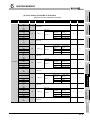
Function Details of D/A Conversion ••••••••••••••••••••••••••••••••••••••••••••••••••••••••••••••••••••••••••• 4 - 25
A-7
4.3.1
4.3.2
4.3.3
4.3.4
4.3.5
4.4
D/A output enable/disable function •••••••••••••••••••••••••••••••••••••••••••••••••••••••••••••••••••••• 4 - 25
Analog output HOLD/CLEAR function •••••••••••••••••••••••••••••••••••••••••••••••••••••••••••••••••• 4 - 25
Analog output test during a CPU module STOP •••••••••••••••••••••••••••••••••••••••••••••••••••••• 4 - 27
Scaling function (D/A conversion)•••••••••••••••••••••••••••••••••••••••••••••••••••••••••••••••••••••••• 4 - 28
Shifting function (D/A conversion) ••••••••••••••••••••••••••••••••••••••••••••••••••••••••••••••••••••••• 4 - 31
Details of Common Function•••••••••••••••••••••••••••••••••••••••••••••••••••••••••••••••••••••••••••••••••••• 4 - 33
4.4.1
Analog conversion enable/disable setting •••••••••••••••••••••••••••••••••••••••••••••••••••••••••••••• 4 - 33
CHAPTER5 I/O SIGNALS FOR THE CPU MODULE
5 - 1 to 5 - 10
5.1
List of I/O Signals •••••••••••••••••••••••••••••••••••••••••••••••••••••••••••••••••••••••••••••••••••••••••••••••••••5 - 1
5.2
Details of I/O Signals •••••••••••••••••••••••••••••••••••••••••••••••••••••••••••••••••••••••••••••••••••••••••••••••5 - 2
5.2.1
5.2.2
Input signals ••••••••••••••••••••••••••••••••••••••••••••••••••••••••••••••••••••••••••••••••••••••••••••••••••••5 - 2
Output signals••••••••••••••••••••••••••••••••••••••••••••••••••••••••••••••••••••••••••••••••••••••••••••••••••5 - 9
CHAPTER6 BUFFER MEMORY
6 - 1 to 6 - 38
6.1
Buffer Memory Assignment •••••••••••••••••••••••••••••••••••••••••••••••••••••••••••••••••••••••••••••••••••••••6 - 1
6.2
CH1 A/D Conversion Enable/Disable Setting (Un\G0) •••••••••••••••••••••••••••••••••••••••••••••••••••• 6 - 10
6.3
CH1 Averaging Process Method Setting (Un\G1) •••••••••••••••••••••••••••••••••••••••••••••••••••••••••• 6 - 10
6.4
CH1 Averaging Process (Time/Number of Times) Setting (Un\G2)••••••••••••••••••••••••••••••••••••• 6 - 11
6.5
CH1 A/D Conversion Scaling Enable/Disable Setting (Un\G10)••••••••••••••••••••••••••••••••••••••••• 6 - 11
6.6
CH1 A/D Conversion Scaling Lower Limit Value (Un\G11) and CH1 A/D Conversion Scaling Upper
Limit Value (Un\G12) ••••••••••••••••••••••••••••••••••••••••••••••••••••••••••••••••••••••••••••••••••••••••••••• 6 - 12
6.7
CH1 Input Shifting Amount to Conversion Value (Un\G13)••••••••••••••••••••••••••••••••••••••••••••••• 6 - 13
6.8
CH1 Input Signal Error Detection Setting (Un\G20)•••••••••••••••••••••••••••••••••••••••••••••••••••••••• 6 - 13
6.9
CH1 Input Signal Error Detection Setting Value (Un\G21)•••••••••••••••••••••••••••••••••••••••••••••••• 6 - 14
6.10 CH1 Logging Enable/Disable Setting (Un\G30)••••••••••••••••••••••••••••••••••••••••••••••••••••••••••••• 6 - 14
6.11 CH1 Logging Cycle Setting Value (Un\G31) and CH1 Logging Cycle Unit Setting (Un\G32)•••••• 6 - 15
6.12 CH1 Logging Data Setting (Un\G33) •••••••••••••••••••••••••••••••••••••••••••••••••••••••••••••••••••••••••• 6 - 16
6.13 CH1 Logging Points After Trigger (Un\G34) ••••••••••••••••••••••••••••••••••••••••••••••••••••••••••••••••• 6 - 16
6.14 CH1 Level Trigger Condition Setting (Un\G35) ••••••••••••••••••••••••••••••••••••••••••••••••••••••••••••• 6 - 17
6.15 CH1 Trigger Data (Un\G36)••••••••••••••••••••••••••••••••••••••••••••••••••••••••••••••••••••••••••••••••••••• 6 - 19
6.16 CH1 Trigger Setting Value (Un\G37)•••••••••••••••••••••••••••••••••••••••••••••••••••••••••••••••••••••••••• 6 - 19
6.17 CH1 Digital Output Value (Un\G100, Un\G1700) ••••••••••••••••••••••••••••••••••••••••••••••••••••••••••• 6 - 20
6.18 CH1 Scaling Value (Un\G102, Un\G1710) ••••••••••••••••••••••••••••••••••••••••••••••••••••••••••••••••••• 6 - 21
6.19 CH1 Maximum Digital Output Value (Un\G104, Un\G1720) and CH1 Minimum Digital Output Value
(Un\G106, Un\G1721)•••••••••••••••••••••••••••••••••••••••••••••••••••••••••••••••••••••••••••••••••••••••••••• 6 - 22
6.20 CH1 Maximum Scaling Value (Un\G108, Un\G1740) and CH1 Minimum Scaling Value
(Un\G110, Un\G1741)•••••••••••••••••••••••••••••••••••••••••••••••••••••••••••••••••••••••••••••••••••••••••••• 6 - 23
6.21 CH1 Setting Range (Un\G112) ••••••••••••••••••••••••••••••••••••••••••••••••••••••••••••••••••••••••••••••••• 6 - 24
6.22 CH1 A/D Conversion Completed Flag (Un\G113) •••••••••••••••••••••••••••••••••••••••••••••••••••••••••• 6 - 24
6.23 CH1 Input Signal Error Detection Flag (Un\G114) ••••••••••••••••••••••••••••••••••••••••••••••••••••••••• 6 - 25
A-8
6.24 CH1 Oldest Pointer (Un\G120) ••••••••••••••••••••••••••••••••••••••••••••••••••••••••••••••••••••••••••••••••• 6 - 26
6.25 CH1 Latest Pointer (Un\G121) ••••••••••••••••••••••••••••••••••••••••••••••••••••••••••••••••••••••••••••••••• 6 - 27
6.26 CH1 Logging Data Points (Un\G122) ••••••••••••••••••••••••••••••••••••••••••••••••••••••••••••••••••••••••• 6 - 28
6.27 CH1 Trigger Pointer (Un\G123) •••••••••••••••••••••••••••••••••••••••••••••••••••••••••••••••••••••••••••••••• 6 - 28
6.28 CH1 Latest Error Code (Un\G190), CH1 Error Time (Un\G191 to Un\G194), Latest Error Code
(Un\G1790), and Error Time (Un\G1791 to Un\G1794) •••••••••••••••••••••••••••••••••••••••••••••••••• 6 - 29
6.29 CH5 D/A Conversion Enable/Disable Setting (Un\G800) ••••••••••••••••••••••••••••••••••••••••••••••••• 6 - 30
6.30 CH5 Digital Input Value (Un\G802)•••••••••••••••••••••••••••••••••••••••••••••••••••••••••••••••••••••••••••• 6 - 31
6.31 CH5 D/A Conversion Scaling Enable/Disable Setting (Un\G810) ••••••••••••••••••••••••••••••••••••••• 6 - 32
6.32 CH5 D/A Conversion Scaling Lower Limit Value (Un\G811) and CH5 D/A Conversion Scaling Upper
Limit Value (Un\G812) ••••••••••••••••••••••••••••••••••••••••••••••••••••••••••••••••••••••••••••••••••••••••••• 6 - 33
6.33 CH5 Shifting Amount to Input Value (Un\G813) •••••••••••••••••••••••••••••••••••••••••••••••••••••••••••• 6 - 33
6.34 CH5 Set Value Check Code (Un\G900, Un\G1764) ••••••••••••••••••••••••••••••••••••••••••••••••••••••• 6 - 34
6.35 CH5 Real Conversion Digital Value (Un\G902, Un\G1774) •••••••••••••••••••••••••••••••••••••••••••••• 6 - 35
6.36 CH5 Setting Range (Un\G912)••••••••••••••••••••••••••••••••••••••••••••••••••••••••••••••••••••••••••••••••• 6 - 35
6.37 CH5 HOLD/CLEAR Setting Function (Un\G913) ••••••••••••••••••••••••••••••••••••••••••••••••••••••••••• 6 - 35
6.38 Level Data (Un\G1600 to Un\G1609) ••••••••••••••••••••••••••••••••••••••••••••••••••••••••••••••••••••••••• 6 - 36
6.39 Latest Address of Error History (Un\G1800)••••••••••••••••••••••••••••••••••••••••••••••••••••••••••••••••• 6 - 37
6.40 Error History (Un\G1810 to Un\G1964) ••••••••••••••••••••••••••••••••••••••••••••••••••••••••••••••••••••••• 6 - 37
6.41 CH1 Logging Data Storage Area (Un\G5000 to Un\G14999) •••••••••••••••••••••••••••••••••••••••••••• 6 - 38
CHAPTER7 PREPARATORY PROCEDURES AND SETTING
7 - 1 to 7 - 20
7.1
Handling Precautions •••••••••••••••••••••••••••••••••••••••••••••••••••••••••••••••••••••••••••••••••••••••••••••• 7 - 1
7.2
Preparatory Procedures and Setting ••••••••••••••••••••••••••••••••••••••••••••••••••••••••••••••••••••••••••••7 - 2
7.3
Part Names ••••••••••••••••••••••••••••••••••••••••••••••••••••••••••••••••••••••••••••••••••••••••••••••••••••••••••7 - 3
7.4
Wiring •••••••••••••••••••••••••••••••••••••••••••••••••••••••••••••••••••••••••••••••••••••••••••••••••••••••••••••••••7 - 5
7.4.1
7.4.2
7.4.3
7.5
Setting from GX Developer ••••••••••••••••••••••••••••••••••••••••••••••••••••••••••••••••••••••••••••••••••••• 7 - 12
7.5.1
7.5.2
7.6
Wiring precautions ••••••••••••••••••••••••••••••••••••••••••••••••••••••••••••••••••••••••••••••••••••••••••••7 - 5
External wiring •••••••••••••••••••••••••••••••••••••••••••••••••••••••••••••••••••••••••••••••••••••••••••••••••7 - 8
Wiring of external power supply connector•••••••••••••••••••••••••••••••••••••••••••••••••••••••••••••••7 - 9
Intelligent function module detailed setting••••••••••••••••••••••••••••••••••••••••••••••••••••••••••••• 7 - 12
Intelligent function module switch setting••••••••••••••••••••••••••••••••••••••••••••••••••••••••••••••• 7 - 14
Offset/Gain Correction ••••••••••••••••••••••••••••••••••••••••••••••••••••••••••••••••••••••••••••••••••••••••••• 7 - 16
CHAPTER8 UTILITY PACKAGE (GX CONFIGURATOR-AD/GX CONFIGURATOR-DA)
8 - 1 to 8 - 26
8.1
Utility Package Functions •••••••••••••••••••••••••••••••••••••••••••••••••••••••••••••••••••••••••••••••••••••••••8 - 1
8.2
Installing and Uninstalling the Utility Package•••••••••••••••••••••••••••••••••••••••••••••••••••••••••••••••••8 - 2
8.2.1
8.2.2
8.3
Precautions for use •••••••••••••••••••••••••••••••••••••••••••••••••••••••••••••••••••••••••••••••••••••••••••8 - 2
Operating environment••••••••••••••••••••••••••••••••••••••••••••••••••••••••••••••••••••••••••••••••••••••• 8 - 5
Operating the Utility Package•••••••••••••••••••••••••••••••••••••••••••••••••••••••••••••••••••••••••••••••••••••8 - 7
A-9
8.3.1
8.3.2
8.3.3
Common operations ••••••••••••••••••••••••••••••••••••••••••••••••••••••••••••••••••••••••••••••••••••••••••8 - 7
Operation overview •••••••••••••••••••••••••••••••••••••••••••••••••••••••••••••••••••••••••••••••••••••••••••8 - 9
Starting Intelligent function module utility••••••••••••••••••••••••••••••••••••••••••••••••••••••••••••••• 8 - 11
8.4
Initial Setting ••••••••••••••••••••••••••••••••••••••••••••••••••••••••••••••••••••••••••••••••••••••••••••••••••••••• 8 - 14
8.5
Auto Refresh Setting ••••••••••••••••••••••••••••••••••••••••••••••••••••••••••••••••••••••••••••••••••••••••••••• 8 - 16
8.6
Monitor/Test•••••••••••••••••••••••••••••••••••••••••••••••••••••••••••••••••••••••••••••••••••••••••••••••••••••••• 8 - 18
8.6.1
Monitor/Test window•••••••••••••••••••••••••••••••••••••••••••••••••••••••••••••••••••••••••••••••••••••••• 8 - 18
8.7
FB Conversion of Initial Setting/Auto Refresh ••••••••••••••••••••••••••••••••••••••••••••••••••••••••••••••• 8 - 21
8.8
Usage of FB•••••••••••••••••••••••••••••••••••••••••••••••••••••••••••••••••••••••••••••••••••••••••••••••••••••••• 8 - 23
8.8.1
8.8.2
8.8.3
Overview •••••••••••••••••••••••••••••••••••••••••••••••••••••••••••••••••••••••••••••••••••••••••••••••••••••• 8 - 23
Pasting an FB to a sequence program •••••••••••••••••••••••••••••••••••••••••••••••••••••••••••••••••• 8 - 25
Converting (compiling) a sequence program •••••••••••••••••••••••••••••••••••••••••••••••••••••••••• 8 - 26
CHAPTER9 PROGRAMMING
9 - 1 to 9 - 34
9.1
Programming Procedures •••••••••••••••••••••••••••••••••••••••••••••••••••••••••••••••••••••••••••••••••••••••••9 - 2
9.2
Programming for Normal System Configuration ••••••••••••••••••••••••••••••••••••••••••••••••••••••••••••••9 - 4
9.2.1
9.2.2
9.2.3
9.3
Before program creation •••••••••••••••••••••••••••••••••••••••••••••••••••••••••••••••••••••••••••••••••••••9 - 6
Program example using the utility package ••••••••••••••••••••••••••••••••••••••••••••••••••••••••••••••9 - 9
Program example without using the utility package •••••••••••••••••••••••••••••••••••••••••••••••••• 9 - 15
Programming for Remote I/O Network•••••••••••••••••••••••••••••••••••••••••••••••••••••••••••••••••••••••• 9 - 19
9.3.1
9.3.2
9.3.3
Before program creation ••••••••••••••••••••••••••••••••••••••••••••••••••••••••••••••••••••••••••••••••••• 9 - 21
Program example using the utility package •••••••••••••••••••••••••••••••••••••••••••••••••••••••••••• 9 - 22
Program example without using the utility package •••••••••••••••••••••••••••••••••••••••••••••••••• 9 - 27
CHAPTER10 ONLINE MODULE CHANGE
10 - 1 to 10 - 14
10.1
Execution Condition of Online Module Change ••••••••••••••••••••••••••••••••••••••••••••••••••••••••••••• 10 - 2
10.2
Operations During Online Module Change •••••••••••••••••••••••••••••••••••••••••••••••••••••••••••••••••• 10 - 3
10.3
Procedures of Online Module Change•••••••••••••••••••••••••••••••••••••••••••••••••••••••••••••••••••••••• 10 - 4
10.3.1
10.3.2
When the initial setting has been configured with GX Configurator-AD or GX Configurator-DA
•••••••••••••••••••••••••••••••••••••••••••••••••••••••••••••••••••••••••••••••••••••••••••••••••••••••••••••••••• 10 - 4
When the initial setting has been configured with sequence program •••••••••••••••••••••••••••10 - 10
CHAPTER11 TROUBLESHOOTING
11 - 1 to 11 - 11
11.1
Error Code List •••••••••••••••••••••••••••••••••••••••••••••••••••••••••••••••••••••••••••••••••••••••••••••••••••• 11 - 1
11.2
Troubleshooting ••••••••••••••••••••••••••••••••••••••••••••••••••••••••••••••••••••••••••••••••••••••••••••••••••• 11 - 5
11.2.1
11.2.2
11.2.3
11.2.4
11.2.5
11.2.6
11.2.7
A - 10
When "RUN" LED turns off •••••••••••••••••••••••••••••••••••••••••••••••••••••••••••••••••••••••••••••••• 11 - 5
When "ERR" LED turns on or blinks••••••••••••••••••••••••••••••••••••••••••••••••••••••••••••••••••••• 11 - 5
When "ALM" LED blinks ••••••••••••••••••••••••••••••••••••••••••••••••••••••••••••••••••••••••••••••••••• 11 - 5
When digital output values cannot be read••••••••••••••••••••••••••••••••••••••••••••••••••••••••••••• 11 - 6
When A/D conversion completed flag does not turn on during use in normal mode ••••••••••• 11 - 7
When an analog output value is not output •••••••••••••••••••••••••••••••••••••••••••••••••••••••••••• 11 - 7
Checking the Q64AD2DA status ••••••••••••••••••••••••••••••••••••••••••••••••••••••••••••••••••••••••• 11 - 8
APPENDIX
Appendix 1
INDEX
App - 1 to App - 2
External Dimensions •••••••••••••••••••••••••••••••••••••••••••••••••••••••••••••••••••••••••••••••••• App - 1
Index - 1 to Index - 2
A - 11
ABOUT MANUALS
The following manuals are also related to this product.
Order each manual as needed, referring to the following list.
Relevant Manuals
Manual number
Manual name
(model code)
GX Developer Version 8 Operating Manual
Describes the methods for creating, printing, monitoring, and debugging programs with GX
Developer.
SH-080373E
(13JU41)
(Sold separately.)
GX Developer Version 8 Operating Manual (Function Block)
Describes the methods for creating and printing function blocks with GX Developer.
(Sold separately.)
SH-080376E
(13JU44)
GX Works2 Version1 Operating Manual (Common)
System configuration, parameter settings, and online operations (common to Simple project and
Structured project) of GX Works2
SH-080779ENG
(13JU63)
(Sold separately)
Remark
The manuals are included on the CD-ROM for the software package in PDF
format.
The printed manuals are sold separately. When obtaining a manual individually,
order it by quoting the manual number (model code) in the table above.
COMPLIANCE WITH THE EMC AND LOW VOLTAGE DIRECTIVES
(1) For programmable controller system
To configure a system meeting the requirements of the EMC and Low Voltage
Directives when incorporating the Mitsubishi programmable controller (EMC and Low
Voltage Directives compliant) into other machinery or equipment, refer to Chapter 9
"EMC AND LOW VOLTAGE DIRECTIVES" of the QCPU User's Manual (Hardware
Design, Maintenance and Inspection).
The CE mark, indicating compliance with the EMC and Low Voltage Directives, is
printed on the rating plate of the programmable controller.
(2) For the product
For the compliance of this product with the EMC and Low Voltage Directives, refer to
Section 7.4.1 Wiring precautions.
A - 12
GENERIC TERMS AND ABBREVIATIONS
Unless otherwise specified, this manual uses the following generic terms and
abbreviations.
Generic term/
Description
abbreviation
Q64AD2DA
GX Developer
Abbreviation for the Q64AD2DA analog input/output module
Product name of the software package for the MELSEC programmable controllers
GX Works2
GX Configurator-AD
GX Configurator-DA
Abbreviation for analog-digital converter module setting and monitor tool, GX ConfiguratorAD (SW2D5C-QADU-E)
Abbreviation for digital-analog converter module setting and monitor tool, GX-ConfiguratorDA (SW2D5C-QDAU-E)
Generic term for the Q00JCPU, Q00CPU, Q01CPU, Q02CPU, Q02HCPU, Q06HCPU,
Q12HCPU, Q25HCPU, Q02PHCPU, Q06PHCPU, Q12PHCPU, Q25PHCPU, Q12PRHCPU,
Q25PRHCPU, Q00UJCPU, Q00UCPU, Q01UCPU, Q02UCPU, Q03UDCPU, Q04UDHCPU,
QCPU (Q mode)
Q06UDHCPU, Q10UDHCPU, Q13UDHCPU, Q20UDHCPU, Q26UDHCPU, Q03UDECPU,
Q04UDEHCPU, Q06UDEHCPU, Q10UDEHCPU, Q13UDEHCPU, Q20UDEHCPU,
Process CPU
Q26UDEHCPU, Q50UDEHCPU, and Q100UDEHCPU
Generic term for the Q02PHCPU, Q06PHCPU, Q12PHCPU, and Q25PHCPU
Redundant CPU
Generic term for the Q12PRHCPU and Q25PRHCPU
Personal computer
IBM-PC/AT -compatible personal computer
Generic term for analog input ranges of 0 to 10V, 0 to 5V, 1 to 5V, -10 to 10V, 0 to 20mA, and
Factory default setting
4 to 20mA, and for analog output ranges of 0 to 5V, 1 to 5V, -10 to 10V, 0 to 20mA, and 4 to
FB
20mA
Abbreviation for function block
Generic term for the following:
Windows Vista
Microsoft
Windows Vista
Home Basic Operating System,
Microsoft
Windows Vista
Home Premium Operating System,
Microsoft
Windows Vista
Business Operating System,
Microsoft
Windows Vista
Ultimate Operating System,
Microsoft Windows Vista Enterprise Operating System
Generic term for the following:
Windows
XP
Microsoft
Windows
XP Professional Operating System,
Microsoft
Windows
XP Home Edition Operating System
PACKING LIST
The following is included in the package.
Model
Product name
Quantity
Q64AD2DA
Q64AD2DA analog input/output module
External power supply connector
1
1
SW2D5C-QADU-E
SW2D5C-QADU-EA
GX Configurator-AD Version 2 (Single license product) (CD-ROM)
GX Configurator-AD Version 2 (Volume license product) (CD-ROM)
1
1
SW2D5C-QDAU-E
SW2D5C-QDAU-EA
GX Configurator-DA Version 2 (Single license product) (CD-ROM)
GX Configurator-DA Version 2 (Volume license product) (CD-ROM)
1
1
A - 13
1
OVERVIEW
CHAPTER1
OVERVIEW
This user's manual provides the specifications, handling instructions, programming
procedures, and other information of the Q64AD2DA analog input/output module
(hereinafter the "Q64AD2DA"), which is designed to use with the MELSEC-Q series CPU
module.
1.1
Features
(1) Analog input and output using a module
The Q64AD2DA can perform both A/D conversion using four channels and D/A
conversion using two channels.
(2) Ranges can be set for each channel
Various voltage or current range can be set for each channel.
Also, the ranges can be switched by using GX Developer.*1
* 1 Set in Switch setting for I/O and intelligent function module dialog box.
(3) Switching resolution mode
A resolution can be selected from a normal resolution mode (1/4000) and high
resolution mode (1/12000 or 1/16000).*2
* 2 Set in Switch setting for I/O and intelligent function module dialog box.
(4) Scaling function
Digital output values can be converted to scaling values (ratio (%)) and the converted
values can be stored into buffer memory.
In D/A conversion, an input range of digital input values can be changed to a setting
range and the analog output can be performed.
(5) Shifting function
In A/D conversion, a given value is added to an A/D converted digital output value.
In D/A conversion, a given value is added to a digital input value and an analog value
is output.
Changing a shifting quantity reflects the output value in real time. Therefore, the
output value can be adjusted with the shifting function when the CPU is powered on.
(6) Input range extended mode function
The analog input range, 4 to 20mA and 1 to 5V can be increased to the input range of
0 to 22mA and 0 to 5.5V, respectively.*3
A/D conversion can be performed even if the input range falls below 4mA or 1V, when
sensors do not measure concrete values.
Combining the input range extended mode function and input signal error detection
function detects a disconnection.
* 3 Set in Switch setting for I/O and intelligent function module dialog box.
1-1
1.1 Features
OVERVIEW
1
2
SYSTEM
CONFIGURATION
The A/D converted digital output values can be stored into buffer memory.
Logging data can be stored up to 10000th data point storage area for a channel.
The logging facility logs data every sampling periods in the shortest period.
In addition, the logging facility logs large volumes of data at high speeds, resulting in
improving efficiency of debugging.
OVERVIEW
(7) Logging facility
The number of sequence programs can be reduced since GX Configurator-AD or GX
Configurator-DA*1 (sold separately) allows the Q64AD2DA settings on the dialog box.
Also, GX Configurator-AD or GX Configurator-DA simplifies checking of the module
settings and operation status.
In addition, FB*2 can be automatically created from intelligent function module
parameters set in advance to use them in a sequence program.
* 1 Either GX Configurator-AD or GX Configurator-DA checks the intelligent function module
parameter setting and the setting status or operation status of the Q64AD2DA.
In addition, the setting and status can be checked by installing both GX Configurator-AD and GX
Configurator-DA.
* 2 FB is the function for making a circuit block used in a sequence program repeatedly a part (FB) to
use it in the sequence program.
This function can improve the efficiency of program development and minimize program bugs to
improve program qualities.
For the details of FB, refer to GX Developer Version 8 Operating Manual (Function
Block).
3
SPECIFICATIONS
(9) Easy setting using GX Configurator-AD or GX Configurator-DA
4
FUNCTION
Modules can be changed without the system being stopped.
5
I/O SIGNALS FOR
THE CPU MODULE
(8) Online module change
BUFFER MEMORY
6
PREPARATORY
PROCEDURES AND
SETTING
7
8
UTILITY PACKAGE
(GX Configurator-AD/GX
Configurator-DA)
1
1.1 Features
1-2
2
SYSTEM CONFIGURATION
CHAPTER2
SYSTEM CONFIGURATION
This chapter explains the system configuration of the Q64AD2DA.
2.1
Applicable Systems
This section describes the applicable systems.
(1) Applicable modules and base units, and number of modules
(a) When mounted with CPU module
The table below shows the CPU modules and base units applicable to the
Q64AD2DA and the number of modules to be mounted.
Depending on the combination with other modules or the number of mounted
modules, power supply capacity may be insufficient.
Pay attention to the power supply capacity before mounting modules, and if the
power supply capacity is insufficient, change the combination of the modules.
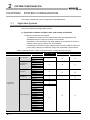
Table 2.1 Applicable modules, number of mountable modules, and applicable base units (1/2)
Applicable CPU module
CPU type
CPU model
Q00JCPU
Basic model QCPU
Q00CPU
Q01CPU
Number of modules*1
16
24
Q02CPU
High performance
model QCPU
Q02HCPU
Q06HCPU
64
Q12HCPU
Q25HCPU
Q02PHCPU
Process CPU
Q06PHCPU
Q12PHCPU
64
Q25PHCPU
Redundant CPU
Q12PRHCPU
Q25PRHCPU
Q00UJCPU
Q00UCPU
Q01UCPU
Programmable
controller CPU
Q02UCPU
53
16
24
36
Q03UDCPU
Q04UDHCPU
Q06UDHCPU
Q10UDHCPU
Q13UDHCPU
Universal model QCPU
Q20UDHCPU
Q26UDHCPU
Q03UDECPU
Q04UDEHCPU
Q06UDEHCPU
Q10UDEHCPU
Q13UDEHCPU
Q20UDEHCPU
Q26UDEHCPU
Q50UDEHCPU
Q100UDEHCPU
2-1
2.1 Applicable Systems
64
Base unit*2
Main base unit
Extension base unit
2
SYSTEM CONFIGURATION
1
Table 2.1 Applicable modules, number of mountable modules, and applicable base units (2/2)
CPU model
Safety CPU
QS001CPU
Base unit*2
Main base unit
Extension base unit
*3
Not applicable
Q06CCPU-V
C Controller module
Q06CCPU-V-B
OVERVIEW
CPU type
Programmable
controller CPU
Number of modules*1
2
64
Q12DCCPU-V
: Applicable,
: Not applicable
* 1 Limited within the range of I/O points for the CPU module.
* 2 Can be installed to any I/O slot of a base unit.
* 3 The safety CPU cannot be connected with extension base units.
SYSTEM
CONFIGURATION
Applicable CPU module
3
Remark
SPECIFICATIONS
For the use of the C Controller module, refer to C Controller Module User's
Manual.
FUNCTION
4
I/O SIGNALS FOR
THE CPU MODULE
5
BUFFER MEMORY
6
PREPARATORY
PROCEDURES AND
SETTING
7
UTILITY PACKAGE
(GX Configurator-AD/GX
Configurator-DA)
8
2.1 Applicable Systems
2-2
2
SYSTEM CONFIGURATION
(b) When mounted with MELSECNET/H remote I/O station
The table below shows the network modules and base units applicable to the
Q64AD2DA and the number of network modules to be mounted.
Depending on the combination with other modules or the number of mounted
modules, power supply capacity may be insufficient.
Pay attention to the power supply capacity before mounting modules, and if the
power supply capacity is insufficient, change the combination of the modules.
Table 2.2 Applicable modules, number of mountable modules, and applicable base units
Applicable network module
Number of
modules*1
Base unit*2
Main base unit of
Extension base unit of
remote I/O station
remote I/O station
QJ72LP25-25
QJ72LP25G
QJ72LP25GE
64
QJ72BR15
: Applicable,
: Not applicable
* 1 Limited within the range of I/O points for the network module.
* 2 Can be installed to any I/O slot of a base unit.
Remark
The Basic model QCPU or C Controller module cannot create the
MELSECNET/H remote I/O network.
(2) Support of multiple CPU system
When using the Q64AD2DA in a multiple CPU system, refer to the following manual
first.
• QCPU User's Manual (Multiple CPU System)
(a) Supported Q64AD2DA
The function version of the Q64AD2DA has been "C" from the first release,
supporting the multiple CPU system.
(b) Intelligent function module parameters
Write intelligent function module parameters only to the control CPU of the
Q64AD2DA.
(3) Support of online module change
The function version of the Q64AD2DA has been "C" from the first release, supporting
online module change.
For details, refer to CHAPTER 10.
2-3
2.1 Applicable Systems
2
SYSTEM CONFIGURATION
1
Table 2.3 Compatible software package and software version
Software version
System
GX Developer*2
Q00J/Q00/
Single CPU system
Version 7 or later
Q01CPU
Multiple CPU system
Version 8 or later
Q02/Q02H/Q06H/ Single CPU system
Version 4 or later
Q12H/Q25HCPU
Multiple CPU system
Version 6 or later
Q02PH/
Single CPU system
Q06PHCPU
Multiple CPU system
Q12PH/
Single CPU system
Q25PHCPU
Multiple CPU system
Q12PRH/
Redundant CPU
Q25PRHCPU
system
Q00UJ/Q00U/
Single CPU system
Q01UCPU
Multiple CPU system
Q02U/Q03UD/
Single CPU system
Version 8.68W or later
Cannot be used
Version 7.10L or later
4
Multiple CPU system
Q13UDH/
Single CPU system
Q26UDHCPU
Multiple CPU system
Q03UDE/
Single CPU system
Version 8.48A or later
FUNCTION
Version 2.10L or later Version 2.10L or later
5
Version 8.76E or later
Version 1.08J or later
Version 8.62Q or later
6
Version 8.68W or later
Q06UDEH/
Multiple CPU system
Q26UDEHCPU
Q10UDEH/
Single CPU system
Q20UDEHCPU
Multiple CPU system
Q50UDEH/
Single CPU system
Q100UDEHCPU
Multiple CPU system
When mounted to MELSECNET/H remote
I/O station
Version 8.76E or later
Cannot be used
Version 6 or later
I/O SIGNALS FOR
THE CPU MODULE
Single CPU system
Version 8.76E or later
Cannot be used
Cannot be used
Version 1.31H or later
Version 2.10L or later Version 2.10L or later
Cannot be used
* 1 The setting of intelligent function module parameters for A/D conversion and D/A conversion, the
setting status, and operating status can be checked by installing either GX Configurator-AD or GX
Configurator-DA.
The setting and setting states can be checked with the installed GX Configurator-AD and GX
Configurator-DA.
* 2 For the FB conversion function, use GX Developer 8 or later.
POINT
Depending on the version of GX Configurator-AD and GX Configurator-DA, CPU
modules and functions of the Q64AD2DA vary.
2.1 Applicable Systems
2-4
BUFFER MEMORY
Multiple CPU system
Q20UDHCPU
Q13UDEH/
Version 1.08J or later
Version 8.45X or later
Q10UDH/
Q04UDEH/
Version 1.10N or later
3
7
PREPARATORY
PROCEDURES AND
SETTING
Q06UDHCPU
GX Works2
8
UTILITY PACKAGE
(GX Configurator-AD/GX
Configurator-DA)
Q04UDH/
GX Configurator-AD GX Configurator-DA
2
SYSTEM
CONFIGURATION
The software packages, GX Configurator-AD and GX Configurator-DA*1, are not
required. The intelligent function module parameter setting, setting status, and
operating status can be checked easily by using the packages.
The software versions compatible with GX Developer, GX Configurator-AD, GX
Configurator-DA, and GX Works2 are listed in the Table 2.3.
SPECIFICATIONS
Operating the Q64AD2DA requires GX Developer whose version is compatible with
the CPU system to be used.
OVERVIEW
(4) Supported software packages
2
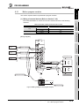
2.2
SYSTEM CONFIGURATION
Using the Q64AD2DA with Redundant CPU
(1) GX Configurator-AD and GX Configurator-DA
GX Configurator-AD and GX Configurator-DA cannot be used when accessing the
Redundant CPU via an intelligent function module on an extension base unit from GX
Developer.
Connect a personal computer to the Redundant CPU with a communication path
indicated below.
1
2
Main base unit
Extension base unit
(GX Configurator-AD or GX Configurator-DA
cannot be used.)
1
Connecting directly to a programmable controller CPU
2
Connecting to a programmable controller CPU via an intelligent function module
(Ethernet module, MELSECNET/H module, or CC-Link module) on the main base unit
Figure 2.1 Communication path for GX Configurator-AD and GX Configurator-DA
2-5
2.2 Using the Q64AD2DA with Redundant CPU
1
OVERVIEW
Checking Function Version, Serial Number, and Software
Version
This section describes how to check the function version of the Q64AD2DA and the
software version of GX Configurator-AD or GX Configurator-DA.
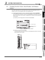
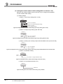
(1) Checking the function version and serial number of the Q64AD2DA
The serial number and function version of the Q64AD2DA are described in the rating
plate, on the front part of the module, or displayed in the System monitor dialog box of
GX Developer.
SYSTEM
CONFIGURATION
2
3
SPECIFICATIONS
(a) Checking on the rating plate on the side of the Q64AD2DA
Function version
4
(b) Checking on the front of the module
The serial number and function version on the rating plate is shown on the front
(at the bottom) of the module.
5
I/O SIGNALS FOR
THE CPU MODULE
Figure 2.2 Rating plate on the side of module
FUNCTION
Relevant regulation
standards
BUFFER MEMORY
6
7
PREPARATORY
PROCEDURES AND
SETTING
2.3
SYSTEM CONFIGURATION
Function version
Serial No.
Figure 2.3 Description on the front part of module
8
UTILITY PACKAGE
(GX Configurator-AD/GX
Configurator-DA)
2
2.3 Checking Function Version, Serial Number, and Software Version
2-6
2
SYSTEM CONFIGURATION
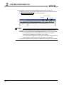
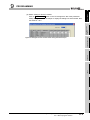
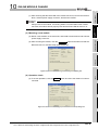
(c) Checking on the System monitor dialog box (Product Information List)
To display the system monitor, select [Diagnostics] [System monitor] and click
the Product Information List button of GX Developer.
Function version
Serial No.
Product No.
Figure 2.4 Checking the serial number and function version
POINT
The serial number displayed on the Product information list dialog box of GX
Developer may differ from that on the rating plate and on the front of the module.
• The serial number on the rating plate and front part of the module
indicates the management information of the product.
• The serial number displayed on the Product information list dialog box of
GX Developer indicates the function information of the product.
The function information of the product is updated when a new function is added.
2-7
2.3 Checking Function Version, Serial Number, and Software Version
SYSTEM CONFIGURATION
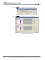
(2) Checking the software version of GX Configurator-AD and GX
Configurator-DA
To check the software version of GX Configurator-AD and GX Configurator-DA,
select [Help] [Product information] of GX Developer.
OVERVIEW
1
SYSTEM
CONFIGURATION
2
SPECIFICATIONS
3
Software version
FUNCTION
4
("Product information" dialog box of GX Developer Version 8)
5
I/O SIGNALS FOR
THE CPU MODULE
Figure 2.5 Product information dialog box
BUFFER MEMORY
6
PREPARATORY
PROCEDURES AND
SETTING
7
8
UTILITY PACKAGE
(GX Configurator-AD/GX
Configurator-DA)
2
2.3 Checking Function Version, Serial Number, and Software Version
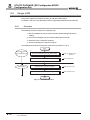
2-8
3
SPECIFICATIONS
CHAPTER3
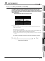
3.1
SPECIFICATIONS
Performance Specifications
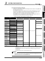
The following table shows the performance specifications of the Q64AD2DA.
Table 3.1 Performance specifications of the Q64AD2DA (1/2)
Item
Number of analog input
points
Analog
input
Specifications
4 points (4 channels)
Voltage
Current
-10 to 10VDC (Input resistance: 1M )
0 to 20mADC (Input resistance: 250 )
Normal resolution mode:-96 to 4095, -4096 to 4095, -1096 to 4595
Digital output
I/O characteristics and
Current
maximum resolution*1
Voltage
Input
High resolution mode:-384 to 16383, -288 to 12287, -16384 to 16383, -3288 to 13787
A/D
conversion area
Analog
input range
0 to 10V
0 to 5V
1 to 5V
-10 to 10V
1 to 5V
(Extended mode)
0 to 20mA
4 to 20mA
4 to 20mA
(Extended mode)
Analog
Accuracy (Accuracy
relative to maximum
Current
digital output value)
Voltage
input range
Ambient
temperature
0 to 10V
-10 to 10V
0 to 5V
1 to 5V
1 to 5V
(Extended mode)
0 to 20mA
4 to 20mA
4 to 20mA
value
High resolution mode
Digital output
Maximum
-4000 to 4000
resolution
2.5mV
1.25mV
1.0mV
2.5mV
-16000 to 16000
resolution
0.625mV
0.416mV
0.333mV
0.625mV
-1000 to 4500
1.0mV
-3000 to 13500
0.333mV
0 to 4000
5 A
4 A
0 to 12000
1.66 A
1.33 A
-1000 to 4500
4 A
-3000 to 13500
1.33 A
0 to 4000
value
0 to 16000
0 to 12000
Normal resolution mode
0 to 55
25 5
High resolution mode
0 to 55
0.4%
( 64digit)
0.4%
( 16digit)
0.4%
( 48digit)
3.1 Performance Specifications
500 s/channel
Voltage:
25 5
0.1%
( 16digit)
0.1%
( 4digit)
(Extended mode)
Conversion speed
Absolute maximum input
3-1
Normal resolution mode
Digital output
Maximum
15V Current:
30mA*2
0.1%
( 12digit)
3
SPECIFICATIONS
1
Table 3.1 Performance specifications of the Q64AD2DA (2/2)
Specifications
Normal resolution mode: -96 to 4095, -4096 to 4095
Digital input
I/O characteristics
and maximum resolution
D/A
conversion area
Analog
output range
0 to 5V
1 to 5V
-10 to 10V
0 to 20mA
4 to 20mA
Normal resolution mode
Digital input
Maximum
value
resolution
1.25mV
1.0mV
2.5mV
5 A
0 to 4000
-4000 to 4000
0 to 4000
relative to maximum
analog output value)
Current Voltage
Accuracy (Accuracy
value
resolution
0.416mV
0.333mV
0.625mV
1.66 A
0 to 12000
-16000 to 16000
0 to 12000
1.33 A
Ambient temperature
0 to 55
output range
0 to 5V
1 to 5V
-10 to 10V
0 to 20mA
4 to 20mA
25 5
0.3% ( 30mV)
0.1% ( 10mV)
0.3% ( 60 A)
0.1% ( 20 A)
4
12V Current: 21mA
Available
protection
Specific isolated
Isolation
area
Between input
method
controller power
Photocoupler
isolation
500VACrms, 1min
Insulation
resistance
500VDC 20M
or more
supply
Between input/output
channels
Between external
6
---
---
---
power supply and
analog input/output
External connection system
Applicable cable size
Applicable solderless terminals
External power supply
Internal current consumption (5VDC)
Weight
5
16 points (I/O assignment: Intelligent 16 points)
A/D conversion area, D/A conversion area:18 points terminal block
External power supply 24VDC, FG terminal connection: External power supply connector
A/D conversion area, D/A conversion area: 0.3 to 0.75mm 2
External power supply 24VDC, FG terminal connection: Refer to Table 3.2.*3
A/D conversion area, D/A conversion area: R1.25-3 (Solderless terminals with sleeves are
unavailable.)
External power supply 24VDC, FG terminal connection: Not available
24VDC 15%
Ripple, spike 500mVP-P or less
Inrush current: 2.5A 150 s or less
Current consumption: 0.19A
0.17A
0.23kg
7
8
* 1 For the details of the I/O conversion characteristic, refer to Section 3.2.1.
* 2 Indicates the value of the instant input current that does not break module inner electrical
resistance. The maximum input current value is 24mA when the current is impressed steadily.
3.1 Performance Specifications
BUFFER MEMORY
terminal and
programmable
Dielectric withstand voltage
I/O SIGNALS FOR
THE CPU MODULE
Voltage:
FUNCTION
500 s/channel
output
Output short-circuit
Number of I/O occupied points
3
PREPARATORY
PROCEDURES AND
SETTING
Conversion speed
Absolute maximum
Insulation specifications
High resolution mode
Digital input
Maximum
4 A
Analog
2
SPECIFICATIONS
Voltage
Current
3-2
UTILITY PACKAGE
(GX Configurator-AD/GX
Configurator-DA)
output
High resolution mode: -288 to 12287, -16384 to 16383
-10 to 10VDC (External load resistance: 1M )
0 to 20mADC (External load resistance: 600 )
Current Voltage Output
Analog
OVERVIEW
2 points (2 channels)
points
SYSTEM
CONFIGURATION
Item
Number of analog output
3
SPECIFICATIONS
* 3 The following shows the specifications of the cable applicable to an external power supply
connector.
Table 3.2 Cable applicable to external power supply connector
Item
Specifications
3.3mm2(AWG12)
Applicable cable size
Size when inserting two
Single wire: 0.2 to 0.8mm2
cables into one terminal
Stranded wire: 0.2 to 0.8mm2
Screw tightening torque
2
2
0.5 to 0.6N m
External power supply
connector (accessory)
Figure 3.1 When inserting two cables into one terminal
Remark
For general specifications of the Q64AD2DA, refer to the user's manual for the
CPU module used.
3-3
3.1 Performance Specifications
1
[Offset value]
The offset value refers to the analog input value (voltage or current) that makes the
digital output value be 0.
3
4
FUNCTION
[Gain value]
The gain value refers to the analog input value (voltage or current) that makes the
digital output value be:
• 4000 (in normal resolution mode)
• 16000 or 12000 (in high resolution mode)
2
SYSTEM
CONFIGURATION
The I/O conversion characteristic of A/D conversion represents the angle formed by a
straight line connecting the "offset value" and "gain value" when the analog signals
(voltage or current input) from outside the programmable controller are converted to digital
values.
SPECIFICATIONS
I/O conversion characteristic of A/D conversion
I/O SIGNALS FOR
THE CPU MODULE
5
6
BUFFER MEMORY
3.2.1
OVERVIEW
I/O Conversion Characteristic
7
PREPARATORY
PROCEDURES AND
SETTING
3.2
SPECIFICATIONS
8
UTILITY PACKAGE
(GX Configurator-AD/GX
Configurator-DA)
3
3.2 I/O Conversion Characteristic
3.2.1 I/O conversion characteristic of A/D conversion
3-4
3
SPECIFICATIONS
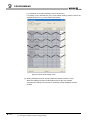
(1) Voltage input characteristic
Figure 3.2 shows voltage input characteristics.
2) 0 to 5V
Practical analog input range
1) 1 to 5V
Practical analog input range
High resolution
mode
High resolution
mode
12287
12000
12287
12000
Normal resolution
mode
Digital output value
Digital output value
Normal resolution
mode
4095
4000
0
0
-96
-288
4095
4000
0
-96
-288
0
5
Analog input voltage (V)
01
5
Analog input voltage (V)
3) -10 to 10V
4) 0 to 10V
Practical analog input range
16383
16000
0
0
Normal resolution mode
-4000
-4096
-10
5) 1 to 5V (Extended mode)
Digital output value
Digital output value
High resolution mode
4095
4000
4095
4000
0
-96
-384
0
10
Analog input voltage (V)
Practical analog input range
High resolution mode
13787
13500
Digital output value
Normal resolution
mode
4595
4500
0
-1000
-1096
-3000
-3288
0
01
5.5
Analog input voltage (V)
Figure 3.2 Voltage input characteristic
3-5
Practical analog input range
16383
16000
High resolution mode
-16000
-16384
0
3.2 I/O Conversion Characteristic
3.2.1 I/O conversion characteristic of A/D conversion
0
Normal resolution mode
0
10
Analog input voltage (V)
SPECIFICATIONS
1
Table 3.3 Digital output values in the case of an analog value, exceeding the range
for the digital output value, being entered
setting
1 to 5V
0 to 5V
Digital output value
Digital output value
(normal resolution mode)
(high resolution mode)
Minimum
-96
-10 to 10V
-4096
0 to 10V
-96
1 to 5V
(Extended mode)
Maximum
-1096
4095
Minimum
Maximum
-288
12287
-16384
-384
4595
-3288
16383
3
4
13787
FUNCTION
Analog input range
2
SYSTEM
CONFIGURATION
(2) Do not input an analog input voltage of 15 V or more. The input element
may be damaged.
(3) If an analog value that exceeds the range for the digital output value is
entered, the digital output value will be fixed at the maximum or minimum
value.
SPECIFICATIONS
(1) Set each input range within the practical analog input range and digital output
range. If these ranges are exceeded, the maximum resolution and accuracy
may not fall within the performance specifications. (Avoid using the dotted line
area shown in Figure 3.2.)
OVERVIEW
POINT
I/O SIGNALS FOR
THE CPU MODULE
5
BUFFER MEMORY
6
PREPARATORY
PROCEDURES AND
SETTING
7
8
UTILITY PACKAGE
(GX Configurator-AD/GX
Configurator-DA)
3
3.2 I/O Conversion Characteristic
3.2.1 I/O conversion characteristic of A/D conversion
3-6
3
SPECIFICATIONS
(2) Current input characteristic
Figure 3.3 shows current input characteristics.
Practical analog input range
1) 4 to 20mA
2) 0 to 20mA
Practical analog input range
High resolution
mode
High resolution
mode
12287
12000
12287
12000
Normal resolution
mode
4095
4000
Digital output value
Digital output value
Normal resolution
mode
0
0
-96
-288
4095
4000
0
-96
-288
0 4
20
Analog input current (mA)
3) 4 to 20mA (Extended mode)
Practical analog input range
13787
13500
Digital output value
High resolution
mode
Normal resolution
mode
4595
4500
0
-1000
-1096
-3000
-3288
0
0 4
22
Analog input current (mA)
Figure 3.3 Current input characteristic
3-7
3.2 I/O Conversion Characteristic
3.2.1 I/O conversion characteristic of A/D conversion
0
0
20
Analog input current (mA)
SPECIFICATIONS
1
Table 3.4 Digital output values in the case of an analog value, exceeding the range
for the digital output value, being entered
Analog input range
setting
4 to 20mA
0 to 20mA
4 to 20mA
Digital output value
(high resolution mode)
Minimum
Maximum
Minimum
Maximum
-96
4095
-288
12287
-1096
4595
-3288
13787
3
4
FUNCTION
(Extended mode)
Digital output value
(normal resolution mode)
SYSTEM
CONFIGURATION
(2) Do not input an analog input current of 30 mA or more. The input elements
may be damaged.
(3) If an analog value that exceeds the range of the digital output value is
entered, the digital output value will be fixed at the maximum or minimum
value.
2
SPECIFICATIONS
(1) Set each input range within the practical analog input range and digital output
range.
If these ranges are exceeded, the maximum resolution and accuracy may not
fall within the performance specifications. (Avoid using the dotted line area
shown in Figure 3.3.)
OVERVIEW
POINT
I/O SIGNALS FOR
THE CPU MODULE
5
BUFFER MEMORY
6
PREPARATORY
PROCEDURES AND
SETTING
7
8
UTILITY PACKAGE
(GX Configurator-AD/GX
Configurator-DA)
3
3.2 I/O Conversion Characteristic
3.2.1 I/O conversion characteristic of A/D conversion
3-8
3
SPECIFICATIONS
3.2.2
I/O conversion characteristic of D/A conversion
The I/O conversion characteristic of D/A conversion represents the angle formed by a
straight line connecting the "offset value" and "gain value" when converting the digital input
value written from the CPU module to an analog output value (voltage or current output).
[Offset value]
The offset value refers to the analog output value (voltage or current) when the digital
input value set from the CPU module is 0.
[Gain value]
The gain value is the analog output value (voltage or current) when the digital input
value set from the CPU module is:
• 4000 (in normal resolution mode)
• 12000 (when 1 to 5V, 0 to 5V, 4 to 20mA, or 0 to 20mA selected in high resolution
mode)
• 16000 (when -10 to 10V is selected in high resolution mode)
3-9
3.2 I/O Conversion Characteristic
3.2.2 I/O conversion characteristic of D/A conversion
3
SPECIFICATIONS
1
(1) Voltage output characteristic
1
0
0
High resolution
mode
5
0
0
High resolution
mode
-288 -96 0 4000 4095 12000 12287
Digital input value
-288 -96 0 4000 4095 12000 12287
Digital input value
2
3
SPECIFICATIONS
Analog output voltage (V)
5
Normal resolution
mode
Analog output voltage (V)
Practical analog output range
Normal resolution
mode
Practical analog output range
2) 0 to 5V
SYSTEM
CONFIGURATION
1) 1 to 5V
OVERVIEW
Figure 3.4 shows voltage output characteristics.
4
3) -10 to 10V
10
High resolution
mode
FUNCTION
5
I/O SIGNALS FOR
THE CPU MODULE
0
-4096 -4000
0
4000 4095
Digital input value
16000 16383
Figure 3.4 Voltage output characteristic
POINT
Set each output range within the practical digital input range and analog output
range.
If these ranges are exceeded, the maximum resolution and accuracy may not fall
within the performance specifications. (Avoid using the dotted line area shown in
Figure 3.4.)
7
8
UTILITY PACKAGE
(GX Configurator-AD/GX
Configurator-DA)
-16384 -16000
BUFFER MEMORY
6
-10
PREPARATORY
PROCEDURES AND
SETTING
0
Practical analog output range
Analog output voltage (V)
Normal resolution
mode
3.2 I/O Conversion Characteristic
3.2.2 I/O conversion characteristic of D/A conversion
3 - 10
3
SPECIFICATIONS
(2) Current output characteristic
Figure 3.5 shows current output characteristics.
Analog output current (mA)
20
4
0
0
High resolution
mode
Normal resolution
mode
20
Analog output current (mA)
Practical analog output range
Normal resolution
mode
0
-288 -96 0
4000 4095 12000 12287
Digital input value
0
High resolution
mode
Practical analog output range
2) 0 to 20mA
1) 4 to 20mA
-288 -96 0 4000 4095 12000 12287
Digital input value
Figure 3.5 Current output characteristic
POINT
Set each output range within the practical digital input range and analog output
range.
If these ranges are exceeded, the maximum resolution and accuracy may not fall
within the performance specifications. (Avoid using the dotted line area shown in
Figure 3.5.)
3 - 11
3.2 I/O Conversion Characteristic
3.2.2 I/O conversion characteristic of D/A conversion
FUNCTION
1
Function List
Table 4.1 Function list
Item
Reference
Function
(1)
section
Sampling processing
The A/D conversion for analog input values is performed successively
for each channel, and the digital output value is output upon each
4
conversion. The value is stored in buffer memory.
Averaging processing
The digital output value is averaged on a channel basis and the
averaged value is stored in buffer memory.
Section
4.2.1
FUNCTION
(2)
A/D conversion method
The averaging processing has three methods as follows:
Maximum and minimum values
hold function
A/D
Scaling function (A/D
conversion
conversion)
function
(1)
(a)
Time average
(b)
Count average
(c)
Moving average
5
This function retains the maximum and minimum values of the digital
output values and scaling values in the module.
(2)
The retained values can be reset in any timing.
This function converts digital output values to scaling values and stores the
converted values into buffer memory.
Time to configure a program for scaling can be decreased.
Section
4.2.2
Section
4.2.3
The digital output value can be adjusted easily with the shifting function when
Shifting function (A/D
the CPU is powered on.
conversion)
The shifting function adds a setting quantity to a digital output value and
Section
4.2.4
stores the value into buffer memory.
This function detects voltage or current input values exceeding the setting
Input signal error detection
ranges.
function
A channel set to averaging processing can be checked every sampling
Section
4.2.5
processing.
Input range extended mode
function
This function increases input ranges.
Combining the input range extended mode function and input signal error
detection function detects a disconnection.
Section
4.2.6
This function performs logging of the digital values that A/D conversion is
performed.
Section
Logging data can be stored up to 10000th data point and time-series data that
4.2.7
A/D conversion is performed can be referred and stored easily.
6
7
8
UTILITY PACKAGE
(GX Configurator-AD/GX
Configurator-DA)
Logging facility
SPECIFICATIONS
3
Table 4.1 lists the functions of the Q64AD2DA.
I/O SIGNALS FOR
THE CPU MODULE
4.1
2
SYSTEM
CONFIGURATION
The device numbers (X or Y) and buffer memory addresses described in this chapter are
used for CH1. (The device numbers and buffer memory addresses specified in D/A
conversion are used for CH5.)
For the device numbers and buffer memory addresses used for other channels, refer to
Section 5.1 and Section 6.1.
OVERVIEW
FUNCTION
BUFFER MEMORY
CHAPTER4
PREPARATORY
PROCEDURES AND
SETTING
4
4.1 Function List
4-1
4
FUNCTION
Table 4.1 Function list
Item
Function
(1)
function
(2)
section
This function sets whether D/A conversion values are output or offset
values are output for each channel.
D/A output enable/disable
Reference
The conversion speed does not change regardless of whether CH5
Section
4.3.1
Output enable/disable flag (Y5) is enabled (ON) or disabled (OFF).
Analog output HOLD/CLEAR
This function retains an output analog value for the case where the CPU
function
module is placed in STOP or in a stop error status.
D/A
Analog output test during a CPU
conversion
module STOP
function
Scaling function (D/A
conversion)
When CH5 Output enable/disable flag (Y5) is set to on forcibly while the CPU
module is placed in STOP status, the analog value that D/A conversion is
performed is output.
This function changes an input range of digital input values to a given range
between -32000 and 32000.
Time to configure a program for scaling can be decreased.
Section
4.3.2
Section
4.3.3
Section
4.3.4
The digital input value can be adjusted easily with the shifting function when
Shifting function (D/A
the CPU is powered on.
conversion)
The shifting function adds a setting quantity to a digital input value and stores
Section
4.3.5
the value into buffer memory.
(1)
This function sets whether A/D or D/A conversion for each channel is
(2)
Setting the channels not to be used to be disabled decreases sampling
enabled or disabled.
Analog conversion enable/
disable setting
periods.
(3)
Section
4.4.1
The analog conversion enable/disable setting is set to be disabled for all
channels conversion in default configuration.
Common
(1)
function
A resolution can be selected from a normal resolution mode (1/4000)
and high resolution mode (1/12000 or 1/16000).
Resolution mode
Section
3.1
(2)
Setting a resolution mode is performed for all the channels at once.
(3)
For details of a digital output value, digital input value, and a maximum
Section
resolution in normal resolution mode or high resolution mode, refer to
7.5
Section 3.1.
Online module change
4-2
4.1 Function List
Modules can be changed without the system being stopped.
CHAPTER
10
1
(1) Sampling period of the Q64AD2DA
A/D conversion is performed from CH1 to CH4 and D/A conversion is performed from
CH5 to CH6 in series in 500 s per channel for the Q64AD2DA.
Sampling period is the period of renewing digital output values.
The period of renewing digital output values varies depending on the total number of
channels enable A/D conversion and D/A conversion.
2
SYSTEM
CONFIGURATION
A/D conversion methods
Averaging processing requires at least two times of conversion processing excluding
the maximum and the minimum values.
After the first averaging processing is completed, A/D conversion completed flag (XE)
is set to on.
(a) Time average
A/D conversion is made for the preset period of time, and the sum of values
excluding maximum and minimum values is averaged, resulting in storing into the
buffer memory.
The processing times within the set time varies depending on the number of
channels used (total number of channels enable A/D conversion and D/A
conversion).
The processing times within the set time is shown below.
Setting time
Processing times =
(Times)
(Numbers of channels to be used
4
FUNCTION
(3) Averaging processing
5
I/O SIGNALS FOR
THE CPU MODULE
A/D conversion is made successively for analog input values, and the converted
digital output values are stored in buffer memory.
SPECIFICATIONS
3
(2) Sampling processing
6
0.5)
BUFFER MEMORY
4.2.1
OVERVIEW
Function Details of A/D Conversion
[Example] Processing times under the following setting
• Number of channels used
4CH
A/D conversion: CH1, CH2, and CH3
D/A conversion: CH5
• Setting time
15ms
7
PREPARATORY
PROCEDURES AND
SETTING
4.2
FUNCTION
15
= 7.5 (times)
The figures after the decimal fractions are omit.
(4 0.5)
Seven times conversion processing are performed
and the average value is output.
(7 4 0.5 = 14(ms) The average value is output every 14(ms).)
8
UTILITY PACKAGE
(GX Configurator-AD/GX
Configurator-DA)
4
4.2 Function Details of A/D Conversion
4.2.1 A/D conversion methods
4-3
4
FUNCTION
POINT
Set the setting time that meets the following condition for time averaging
processing. If the setting time does not meet the following condition, an error
(error code: 202) occurs and the digital output value changes to 0.
• Setting time Minimum processing times 4 (times) 0.5(ms) Number
of channels to be used (total number of A/D conversion and D/A
conversion)
[Example] Number of channels to be used: Six channels
• Setting time (4 6 0.5)
Set the setting time to 12ms or higher.
(b) Count average
A/D conversion is made the preset number of times, and the sum of values
excluding the maximum and minimum values is averaged, resulting in storing into
the buffer memory.
The time required for the count-based average value to be stored into the buffer
memory varies depending on the number of channels used (number of channels
enable A/D conversion and D/A conversion).
Processing time
Set count
(Number of channels to be used
0.5) (ms)
[Example] Processing time under the following setting
• Number of channels used
4CH
A/D conversion: CH1, CH2, and CH3
D/A conversion: CH5
• Set count
20 times
20 4 0.5 40(ms)
The averaged values are output every 40(ms).
POINT
Count average processing requires at least two times of conversion processing
excluding the maximum and the minimum values. Set the setting time to four
times or more.
4-4
4.2 Function Details of A/D Conversion
4.2.1 A/D conversion methods
FUNCTION
(c) Moving average
The digital output values imported per sampling period are averaged to find a
value, which is then stored into the buffer memory.
Since average processing is made with data shifted per sampling, the most recent
digital output value is obtainable.
16000
2)
3)
4)
5)
1)
6)
7)
8)
9)
12)
10) 11)
3
SPECIFICATIONS
8000
1st storage (a)
2nd storage (b)
3rd storage (c)
0
Time [ms]
0
(a)
(b)
4
(c)
ON
A/D conversion
completed flag (XE)
FUNCTION
CH1 Digital output
value (Un\G100)
2
SYSTEM
CONFIGURATION
Sampling period
A/D conversion value
OVERVIEW
1
Data transition in buffer memory
2nd storage (b)
3rd storage (c)
1) + 2) + 3) + 4)
2) + 3) + 4) + 5)
3) + 4) + 5) + 6)
4
4
4
5
I/O SIGNALS FOR
THE CPU MODULE
1st storage (a)
Figure 4.1 Moving average processing in the case of four setting times
BUFFER MEMORY
6
PREPARATORY
PROCEDURES AND
SETTING
7
8
UTILITY PACKAGE
(GX Configurator-AD/GX
Configurator-DA)
4
4.2 Function Details of A/D Conversion
4.2.1 A/D conversion methods
4-5
4
FUNCTION
4.2.2
Maximum and minimum values hold function
The maximum and minimum digital output value and scaling value are held in the buffer
memory for each channel.
(1) Setting methods
(a) The maximum and minimum values are stored into the following buffer memory
when conversions start.
• CH1 Maximum digital output value (Un\G104)
• CH1 Minimum digital output value (Un\G106)
• CH1 Maximum scaling value (Un\G108)
• CH1 Minimum scaling value (Un\G110)
(b) The maximum and minimum values are stored into the buffer memory after the
following states.
• Maximum and minimum values reset request (YD) is set to on.
• Operating condition setting request (Y9) is set to off.
4.2.3
Scaling function (A/D conversion)
This function converts digital output values to scaling values (ratio (%)) and stores the
converted values into buffer memory.
(1) Overview
(a) Whether using the scaling function (A/D conversion) for each channel or not can
be specified with CH1 A/D conversion scaling enable/disable setting (Un\G10).
(b) The scaling function performs scaling conversion of the digital output values set
with CH1 Digital output value (Un\G100) within the range set by the buffer
memory.
• CH1 A/D conversion scaling lower limit value (Un\G11)
• CH1 A/D conversion scaling upper limit value (Un\G12)
(c) The fractional portion of the output value converted with scaling function is
rounded off and stored into CH1 Scaling value (Un\G102).
(d) The setting range allowed for the A/D conversion scaling upper and lower limit
values is -32000 to 32000.
POINT
The setting range allowed for the A/D conversion scaling upper and lower limit
values is -32000 to 32000. Note that the resolution will not change even if an A/D
conversion scaling upper/lower limit value is set to change more than the
resolution.
4-6
4.2 Function Details of A/D Conversion
4.2.2 Maximum and minimum values hold function
FUNCTION
1
• Setting a value corresponding to the upper limit*1 of digital output as the
scaling upper limit value set with CH1 A/D conversion scaling upper limit
value (Un\G12).
• Setting a value corresponding to the lower limit*2 of digital output as the
scaling lower limit value set with CH1 A/D conversion scaling lower limit
value (Un\G11).
* 1 Input range from -10 to 10V, normal resolution: 4000
* 2 Input range from -10 to 10V, normal resolution: -4000
3
SPECIFICATIONS
2) Set Operating condition setting request (Y9) to on.
2
SYSTEM
CONFIGURATION
1) Set the buffer memory as follows:
• Setting CH1 A/D conversion scaling enable/disable setting (Un\G10) to be
enabled (0).
OVERVIEW
(2) Setting methods
FUNCTION
4
I/O SIGNALS FOR
THE CPU MODULE
5
BUFFER MEMORY
6
PREPARATORY
PROCEDURES AND
SETTING
7
8
UTILITY PACKAGE
(GX Configurator-AD/GX
Configurator-DA)
4
4.2 Function Details of A/D Conversion
4.2.3 Scaling function (A/D conversion)
4-7
4
FUNCTION
(3) How to calculate a scaling value
1)
Input range: 0 to 10V, 0 to 5V, 1 to 5V, 0 to 20mA, and 4 to 20mA
Scaling value =
2)
DX
(SH - SL)
+ SL
DMax
Input range: -10 to 10V
Scaling value =
DX (SH - SL) SH + SL
+
DMax - DMin
2
Dx
: CH1 Digital output value (Un/G100)
DMax
: The maximum digital output value in the input range being used
DMin
: The minimum digital output value in the input range being used
SH
: CH1 A/D conversion scaling upper limit value (Un\G12)
SL
: CH1 A/D conversion scaling lower limit value (Un\G11)
[Setting example]
Using the scaling function (A/D conversion) in input range from -10 to 10V and high
resolution mode (from -16000 to 16000)
(a) Setting value
• CH1 A/D conversion scaling upper limit value (Un\G12) SH: 14000
• CH1 A/D conversion scaling lower limit value (Un\G11) SL: 2000
(b) Input value
Digital output value Dx: 7500
Scaling value =
(14000 + 2000)
7500 (14000 - 2000)
+
16000 - ( -16000)
2
= 10812.5
= 10813
Fractional portion is rounded off.
4-8
4.2 Function Details of A/D Conversion
4.2.3 Scaling function (A/D conversion)
FUNCTION
1
The shifting function adds a setting quantity to a digital output value (shifting a digital
output value) and stores the value into buffer memory.
OVERVIEW
Shifting function (A/D conversion)
(c) Changing the shifting amount to conversion value reflects the scaling value in real
time. Therefore, the digital output value can be adjusted with the shifting function
when the CPU is powered on.
(d) If a scaling function (for A/D conversion) is used simultaneously, the value that is
made scaling processing will be shifted.
(2) Setting methods
(a) Set the quantity to be shifted by using CH1 Shifting amount to conversion value
(Un\G13).
(b) Shifting quantities are added to the digital output value set with CH1 Digital output
value (Un\G100) every sampling period, and then the added value is stored into
CH1 Scaling value (Un\G102).
3
SPECIFICATIONS
(b) The shifting amount to conversion value can be set within the range from -32768
to 32767.
4
FUNCTION
(a) The shifted output values are stored into CH1 Scaling value (Un\G102).
SYSTEM
CONFIGURATION
2
(1) Overview
(d) If a value is written to a shifting amount to conversion value, regardless of whether
Operating condition setting request (Y9) is set to on or off, the shifting amount to
conversion value will be added every sampling period.
I/O SIGNALS FOR
THE CPU MODULE
5
(c) The default of shifting amount to conversion value is 0.
BUFFER MEMORY
6
7
PREPARATORY
PROCEDURES AND
SETTING
4.2.4
8
UTILITY PACKAGE
(GX Configurator-AD/GX
Configurator-DA)
4
4.2 Function Details of A/D Conversion
4.2.4 Shifting function (A/D conversion)
4-9
4
FUNCTION
(3) Setting example
For the channel in setting the input range to 0 to 5V and the high resolution mode (to
0 to 12000), I/O characteristic is adjusted as shown below.
1) CH1 Digital output value
(Un\G100)
12000
2) Scaling value
(After adjustment)
11990
+
CH1 Shifting amount to
conversion value
(Un\G13)
+10
1) Digital output value
(Before adjustment)
2) CH1 Scaling value
(Un\G102)
0
Input voltage (V)
5
-10
Input voltage CH1 Digital output value
(V)
(Un\G100)
0
5
Input voltage
(V)
CH1 Scaling value
(Un\G102)
0
5
0
12000
-10
11990
Figure 4.2 I/O characteristic and scaling value after shifting processing
For the case of above example, set CH1 Shifting amount to conversion value
(Un\G13) to 10.
POINT
If the scaling value exceeds the range from -32768 to 32767 after a shifting
processing, the value of lower (-32768) and upper (32767) limits will be fixed.
36000
1) CH1 Digital output value
(Un\G100)
2) Scaling value
32767
+
CH1 Shifting amount to
conversion value
(Un\G13)
+20000
16000
2) CH1 Scaling value
(Un\G102)
4000
0
1) Digital output value
-16000
-10
-5
0
5
10
Input voltage (V)
Figure 4.3 Scaling value for the case of exceeding the range from -32768 to 32767, resulted
from shifting processing
4 - 10
4.2 Function Details of A/D Conversion
4.2.4 Shifting function (A/D conversion)
FUNCTION
1
Input signal error detection function is the function that detects voltage or current input
exceeding a setting range.
OVERVIEW
Input signal error detection function
(d) When the analog input value returns to within the setting range, A/D conversion is
resumed independently of whether CH1 Input signal error detection flag
(Un\G114) and Input signal error detection signal (X7) are reset or not, CH1 A/D
conversion completed flag (Un\G113) of the corresponding channel is set to on
again after the first updating. (ALM LED remains blinking.)
Analog
input value
Error detection
Input signal error
detection upper
limit value
Normal input value
4
5
6
BUFFER MEMORY
CH1 Analog input
value
SPECIFICATIONS
(c) To set CH1 Input signal error detection flag (Un\G114) and Input signal error
detection signal (X7) to off, set Error clear request (YF) to on after the analog input
value returns to within the setting range.
ALM LED turns off immediately after CH1 Input signal error detection flag
(Un\G114) is set to off (0).
FUNCTION
(b) When CH1 Input signal error detection flag (Un\G114) is set to on (1), a digital
output value immediately before the error detection is held for the channel.
In addition, CH1 A/D conversion completed flag (Un\G113) is set to off (0).
3
I/O SIGNALS FOR
THE CPU MODULE
(a) If the input voltage or current rises to or above the input signal error detection
upper limit value or falls to or below the lower limit value, an error occurs under
the following operations.
• CH1 Input signal error detection flag (Un\G114) is set to on (1).
• Input signal error detection signal (X7) is set to on.
• ALM LED blinks.
SYSTEM
CONFIGURATION
2
(1) Overview
Input signal error
detection lower
limit value
7
Time
ON
CH1 Input signal error
detection flag (Un\G114)
PREPARATORY
PROCEDURES AND
SETTING
4.2.5
OFF
ON
Input signal error detection signal (X7)
CH1 A/D conversion
completed flag (Un\G113)
OFF
8
ON
OFF
UTILITY PACKAGE
(GX Configurator-AD/GX
Configurator-DA)
4
ON
Error clear request (YF)
OFF
Figure 4.4 Input signal error detection
4.2 Function Details of A/D Conversion
4.2.5 Input signal error detection function
4 - 11
4
FUNCTION
(e) The input signal error detection is executed at every sampling processing.
(f) The condition of the input signal error detection can be set with CH1 Input signal
error detection setting (Un\G20).
The conditions of the input signal error detection are described in the table below.
Table 4.2 Condition of input signal error detection and operation
CH1 Input signal error
Condition of input signal error detection
detection setting (Un\G20)
Input signal error detection
upper limit value
Error
detection
20mA
If the analog input value reaches to or exceeds
the input signal error detection upper limit
Upper and lower detection (1)
setting value or falls to or below the input
signal error detection lower limit setting value,
Input range
an error is detected.
0mA
Input signal error detection
lower limit value
Error
detection
Not detected
If the analog input value falls to or below the
20mA
input signal error detection lower limit setting
value, an error is detected.
Lower detection (2)
Even if the analog input value reaches to or
Input range
exceeds the input signal error detection upper
limit setting value, an error is not detected.
0mA
If the analog input value exceeds the input
Input signal error detection
lower limit value
Error
detection
Input signal error detection
upper limit value
Error
detection
20mA
signal error detection upper limit setting value,
an error is detected.
Upper detection (3)
Even if the analog input value falls to or below
Input range
the input signal error detection lower limit
setting value, an error is not detected.
0mA
Not detected
Disconnection detection (4)
Disconnection detection is executed.
Refer to Section 4.2.6 (3).
POINT
Setting CH1 Input signal error detection setting (Un\G20) for the channel setting
the following input ranges detects disconnection. (Refer to Section 4.2.6 (3).)
• 4 to 20mA (Extended mode)
• 1 to 5V (Extended mode)
If CH1 Input signal error detection setting (Un\G20) is set to detect disconnection
(4) for the channel setting input ranges other than above ranges, an error (error
code: 212) occurs.
4 - 12
4.2 Function Details of A/D Conversion
4.2.5 Input signal error detection function
FUNCTION
1
1) Set the value for CH1 Input signal error detection setting value (Un\G21) of
corresponding channels in 0.1% increments.
2) Set the value for CH1 A/D conversion enable/disable setting (Un\G0) of
corresponding channels to A/D conversion enable (0).
4) Validate the setting of Operating condition setting request (Y9) from off to on.
Input signal error detection
upper limit value
-
Gain value of each range
Gain value of each range
-
Offset value of each range
1000
(b) Input signal error detection lower limit value
A value that the subtraction of "a value multiplied an input range width (gain value
- offset value) by CH1 Input signal error detection setting value" from a lower limit
value of input range.
The setting is available only when the value is a lower limit value of input range or
less.
=
Lower limit value of each
range
Gain value of each range
-
Input signal error detection
upper limit value
Offset value of each range
1000
FUNCTION
6
7
PREPARATORY
PROCEDURES AND
SETTING
Input signal error detection
setting value
5
I/O SIGNALS FOR
THE CPU MODULE
(a) Input signal error detection upper limit value
A value that the addition of "a value multiplied an input range width (gain value offset value) by CH1 Input signal error detection setting value" to a gain value.
The setting is available only when the value is a gain value or more.
4
BUFFER MEMORY
The setting for upper and lower limit value of input signal error detection is based on
CH1 Input signal error detection setting value (Input signal error detection upper limit
value and Input signal error detection lower limit value). (The value is set in
increments of 1(0.1%))
When the upper and lower detection is set, CH1 Input signal error detection setting
value (Un\G21) is reflected to both upper and lower limit value of input signal error
detection.
SPECIFICATIONS
3
(3) Specifying the upper and lower limit value for the input signal error
detection
=
SYSTEM
CONFIGURATION
2
3) Select the condition of input signal error detection to be used from 1 to 3 in the
Table 4.2 for CH1 Input signal error detection setting (Un\G20) of
corresponding channels.
Input signal error detection
setting value
OVERVIEW
(2) Setting methods
8
UTILITY PACKAGE
(GX Configurator-AD/GX
Configurator-DA)
4
4.2 Function Details of A/D Conversion
4.2.5 Input signal error detection function
4 - 13
4
FUNCTION
The following table shows lower limit values, offset values, and gain values
calculated in setting input ranges.
Table 4.3 Lower limit values, offset values, and gain values calculated by setting input ranges
Input
Voltage
Current
Analog input range
Lower limit value
Offset value
Gain value
0 to 10V
0V
0V
10V
0 to 5V
0V
0V
5V
1 to 5V
1V
1V
5V
-10 to 10V
-10V
0V
10V
1 to 5V (Extended mode)
1V
1V
5V
0 to 20mA
0mA
0mA
20mA
4 to 20mA
4mA
4mA
20mA
4 to 20mA (Extended mode)
4mA
4mA
20mA
(4) Setting examples of the Input signal error detection
[Setting example]
To detect an input signal error when the analog input value is 2.4mA or less, which is
for the analog input range of the channel is set to 4 to 20mA.
(a) Set CH1 Input signal error detection setting value (Un\G21)
The setting values will be turned out when the following values are assigned to the
calculating formula of the input signal error detection lower value described in (3)
of this section.
• Input signal error detection lower limit value: 2.4mA
• Lower limit value of input range (offset value): 4.0mA
• Gain value: 20.0mA
Input signal error
detection setting value
=
4.0
-
2.4
20.0
-
4.0
1000
= 100(10.0%)
Therefore, use "100 (10.0%)" for the setting of CH1 Input signal error detection
setting value (Un\G21).
4 - 14
4.2 Function Details of A/D Conversion
4.2.5 Input signal error detection function
4
FUNCTION
1
OVERVIEW
(b) Set CH1 Input signal error detection setting (Un\G20) in the lower detection (2)
In this case, the value for CH1 Input signal error detection operates as below.
(An error is detected while Upper
and lower detection (1) is set.)
Input signal error detection
upper limit value
2
1.6mA
(10.0 of 1.6mA)
20mA
Gain value
4mA
1.6mA
(10.0 of 1.6mA)
2.4mA
Error
4
Figure 4.5 Setting example1 of Input signal error detection function
5
I/O SIGNALS FOR
THE CPU MODULE
When CH1 Input signal error detection setting (Un\G20) is set in the upper and lower
detection (1), an error will be detected in 21.6mA not only 2.4mA by the setting of "100
(10.0%)"
BUFFER MEMORY
6
PREPARATORY
PROCEDURES AND
SETTING
7
8
UTILITY PACKAGE
(GX Configurator-AD/GX
Configurator-DA)
Input signal error detection
lower limit value
3
SPECIFICATIONS
16mA
(Gain value - Offset value)
FUNCTION
Offset value
SYSTEM
CONFIGURATION
21.6mA
4.2 Function Details of A/D Conversion
4.2.5 Input signal error detection function
4 - 15
4
FUNCTION
4.2.6
Input range extended mode function
The input range extended mode function is the function increasing the input range of 4 to
20mA and 1 to 5V.
Table 4.4 Input range and digital output value for extended mode
Normal mode
Input range
Input range
Extended mode
CH1 Digital output value
Input range
(Un\G100)
Increased
CH1 Digital output value
range
(Un\G100)
4 to 20mA
4 to 20mA
4 to 20mA
(Extended
-96 to 4095
(-288 to 12287)
1 to 5V
0.0 to 22.0mA
-1096 to 4595
mode)
*1
(-3288 to 13787)*1
1 to 5V
1 to 5V
(Extended
0.0 to 5.5V
mode)
* 1 The values in parenthesis refer to the range of digital outputs for setting high resolution
mode.
(1) Overview
(a) The input range extended mode function can monitor the values that fall below
4mA or 1V, so that sensors do not measure concrete values.
4595 (13787)
4500 (13500)
4000 (12000)
4595 (13787)
4500 (13500)
4000 (12000)
Digital output value
Digital output value
(b) The slopes of the lines representing I/O characteristic are same between the
extended mode and the normal mode. However, the input range expands and the
upper and lower limit values of CH1 Digital output value (Un\G100) extend in the
extended mode.
0
-1000 (-3000)
-1096 (-3288)
0
0
4
10
20 22
Expanded range
Expanded range
Analog input current (mA)
The value in parenthesis refers to the digital output value in high resolution mode.
Figure 4.6 I/O characteristic of input range from 4 to 20mA
(Extended mode)
-1000 (-3000)
-1096 (-3288)
0
1
5 5.5
Expanded range
Expanded range
Analog input voltage (V)
The value in parenthesis refers to the digital output value in high resolution mode.
Figure 4.7 I/O characteristic of input range from 1 to 5V
(Extended mode)
(2) Setting methods
Configure the input range (for CH1 to CH4) in "Switch 1" cell of the Switch setting for
I/O and intelligent function module dialog box. (Refer to Section 7.5.2.)
POINT
If the input range extended mode function, scaling function (for A/D conversion),
and shifting function (for A/D conversion) are used simultaneously, the scaling
value can exceed the range from -32768 to 32767.
In such a case, the values set within the upper limit (32767) and lower limit (32767) values will be stored into the buffer memory as scaling values.
4 - 16
4.2 Function Details of A/D Conversion
4.2.6 Input range extended mode function
FUNCTION
1
1) If the conditions described in Table 4.5 are satisfied, the following operations
perform.
• Input signal error detection signal (X7) is set to on.
• CH1 Input signal error detection flag (Un\G114) is set to on (1).
• ALM LED blinks.
To disable the above operations, cancel the conditions of disconnection
detection shown in Table 4.5 and set Error clear request (YF) to on.
Table 4.5 Condition of disconnection detection
Input range
Condition of disconnection detection
4 to 20mA (Extended mode)
Input analog value
2mA
1 to 5V (Extended mode)
Input analog value
0.5V
2) A digital output value immediately before the disconnection detections is held
for CH1 Digital output value (Un\G100), and CH1 A/D conversion completed
flag (Un\G113) is set to off (0).
3) When the disconnection is restored, A/D conversion resumes independently
and CH1 A/D conversion completed flag (Un\G113) is set to on (1) after the
first updating.
POINT
The disconnection detection is executed at every sampling processing regardless
of the status of CH1 Averaging process method setting (Un\G1).
[Example] When the number of conversion enabled channels is three, the
disconnection detection is executed every 1.5ms.
500 s 3CH 1500 s 1.5ms
SYSTEM
CONFIGURATION
SPECIFICATIONS
(b) Operation for disconnection detection
4
FUNCTION
2) To use the disconnection detection function, set CH1 Input signal error
detection setting (Un\G20) to detect disconnections (4), and set Operating
condition setting request (Y9) to on.
3
5
I/O SIGNALS FOR
THE CPU MODULE
1) Disconnection detection can be performed only when the input range is set to
either:
• 4 to 20mA (Extended mode)
• 1 to 5V (Extended mode)
6
BUFFER MEMORY
(a) Setting methods
2
7
PREPARATORY
PROCEDURES AND
SETTING
Combining the input range extended mode function and input signal error detection
function detects a disconnection.
If the input analog current value changes to 2mA or less, or the input analog voltage
value changes 0.5V or less, an external wiring is disconnected, and CH1 Input signal
error detection flag (Un\G114) is set to on (1).
OVERVIEW
(3) Disconnection detection
8
UTILITY PACKAGE
(GX Configurator-AD/GX
Configurator-DA)
4
4.2 Function Details of A/D Conversion
4.2.6 Input range extended mode function
4 - 17
4
FUNCTION
4.2.7
Logging function
(1) Logging function
This function collects the data of the digital output value or scaling value performed
A/D conversion at a preset timing in series.
This function is useful to check the data change of the digital output value or scaling
value performed A/D conversion periodically because the function sets an interval
(logging period), performs logging, and stores the logs into the buffer memory.
In addition, this function is useful to check the data change of the analog input value
during the stopped logging, if a trigger condition is set by using a hold trigger.
(2) Logging operation
When logging starts in sequence programs, logging data are stored into the logging
data storage areas in order from the initial area.
Logging data can be stored up to 10000th data point area for a channel.
The stored data are retained until when the CPU module is powered off or Operating
condition setting request (Y9) is set to on.
Q64AD2DA
Logging data storage area
Specified device data
Digital output value
(Un\G100)
Scaling value
(Un\G102)
Un\G5000
Un\G5001
Un\G5002
Un\G5003
Un\G5004
Un\G5005
1st data
2nd data
3rd data
4th data
5th data
6th data
Un\G14998
Un\G14999
9999th data
10000th data
If data are stored up to 10000th data point area,
data will be overwritten from the 1st data area.
Figure 4.8 Logging operation
4 - 18
4.2 Function Details of A/D Conversion
4.2.7 Logging function
FUNCTION
1
(3) Logging start
OVERVIEW
To use a logging facility, the following items are required for the initial setting.
Start
Initial setting performed by users
2
Logging hold
request signal
SYSTEM
CONFIGURATION
Set the following items.
Logging enable/disable setting
Logging data setting
Logging cycle setting value
Logging cycle unit setting
Logging points after trigger
Which Hold trigger will be used?
Set the item as described bellow.
Set 0 for Level trigger condition setting.
3
SPECIFICATIONS
Level trigger
Set the following items.
Level trigger condition setting
Trigger data
Trigger setting value
Level data
Do not set the following items.
Trigger data
Trigger setting value
4
End
Table 4.6 Initial setting for logging facility
Logging enable/disable
setting
Logging data setting
Logging cycle
Description
Set the item to be enabled (0).
Set whether to perform logging digital output values or scaling
values.
Set the cycle to store data during logging.
Logging points after trigger
Set the amount of logging data after hold triggers are detected
and before logging is held.
Reference
section
Section 6.10
Section 6.12
Section 6.11
Section 6.13
Logging facility
(Refer to (3) in this section )
Initial setting
Logging facility start
6
7
(Refer to (3)(b) in this section )
PREPARATORY
PROCEDURES AND
SETTING
Logging facility hold
5
BUFFER MEMORY
Item
I/O SIGNALS FOR
THE CPU MODULE
(a) Common setting items
To use a logging facility, set the items shown in Table 4.6.
FUNCTION
Figure 4.9 Flowchart of initial setting
Logging hold flag check
(Refer to (4) in this section )
Logging data read and save
8
Logging restart
UTILITY PACKAGE
(GX Configurator-AD/GX
Configurator-DA)
4
End
Figure 4.10 Flowchart of operating procedure
4.2 Function Details of A/D Conversion
4.2.7 Logging function
4 - 19
4
FUNCTION
(b) Hold trigger
Hold trigger is the trigger that occurs for the case of preset trigger conditions to be
met when a logging facility is used.
When the Q64AD2DA detects a hold trigger, the logging facility stops (hold)
collecting logging data after logging the number of preset points.
The necessary setting items vary depending on hold triggers to be used.
Select one of two types of hold trigger.
1) For holding logging in given timing
A hold trigger is detected by using Logging hold request (Y1).
Setting CH1 Logging hold request (Y1) to on holds the logging.
Table 4.7 For detecting hold triggers by using Logging hold request
Item
Reference
Description
section
Level trigger condition setting Set the item to be "Disable" (0).
Section 6.14
ON
OFF
CH1 Logging hold request (Y1)
Hold trigger occurred
CH1 Logging data storage area
(Un\G5000 to Un\G14999)
Logging hold
Data stored before the last
10000 data are discarded.
Logging points after trigger
(Un\G34)
Logging data points (Un\G122)
10000
Figure 4.11 For detecting hold triggers by using Logging hold request
2) For holding logging when given buffer memory meet the setting conditions
A hold trigger is detected by using a level trigger.
Setting CH1 Logging hold request (Y1) to on causes the logging data to be
trigger condition waiting status set in Table 4.8, and the satisfied trigger
condition holds the logging.
Table 4.8 For detecting hold triggers by using level triggers
Item
Description
Level trigger condition setting Set a condition for using level triggers.
Trigger data
Trigger setting value
Set an address of the buffer memory monitoring data to make
level triggers work.
Set a value that makes level triggers work.
Reference
section
Section 6.14
Section 6.15
Section 6.16
This data is the data that monitor data to make level triggers
Level data
work. Set this level data to monitor devices specified for CPU
modules or the like excluding the buffer memory of the
Q64AD2DA and make triggers work.
4 - 20
4.2 Function Details of A/D Conversion
4.2.7 Logging function
Section 6.38
4
FUNCTION
1
ON
Trigger condition enable/disable
Disable
Enable (waiting for trigger condition)
Trigger condition satisfied/not satisfied*1
Not satisfied
Satisfied
Hold trigger occurred
CH1 Logging data storage area
(Un\G5000 to Un\G14999)
OVERVIEW
OFF
2
SYSTEM
CONFIGURATION
CH1 Logging hold request (Y1)
Logging hold
Data stored before latest
10000 are discarded.
3
Logging data points (Un\G122)
SPECIFICATIONS
Logging points after trigger
(Un\G34)
10000
* 1 A hold trigger occurs when the condition set in Table 4.8 is satisfied.
Figure 4.12 For detecting hold triggers by using level triggers
FUNCTION
4
I/O SIGNALS FOR
THE CPU MODULE
5
BUFFER MEMORY
6
PREPARATORY
PROCEDURES AND
SETTING
7
UTILITY PACKAGE
(GX Configurator-AD/GX
Configurator-DA)
8
4.2 Function Details of A/D Conversion
4.2.7 Logging function
4 - 21
4
FUNCTION
POINT
(1) If logging does not start, check the following:
• Is CH1 Logging enable/disable setting (Un\G30) set to be disabled (1)?
If CH1 Logging enable/disable setting (Un\G30) has been set to be
disabled (1), set CH1 Logging enable/disable setting (Un\G30) to be
enabled (0),
• Is the initial setting correct?
If the initial setting has an error, Error flag (XF) is set to on and ERR. LED
lights up.
Reconfigure the initial setting, referring to the error code. (refer to Section
11.1.)
(2) If Operating condition setting request (Y9) is set to on during logging, the
logging will stop whether hold triggers are executed or not and all the stored
logging data will be cleared before Operating condition setting request (Y9) is
set to on.
4 - 22
4.2 Function Details of A/D Conversion
4.2.7 Logging function
4
FUNCTION
1
If CH1 Logging hold flag (X1) is set to on, refer to the buffer memory shown in Figure
4.13 and Figure 4.14.
The logging datad point determines how to refer to the logging data storage area.
2
SYSTEM
CONFIGURATION
[Example] The held logging data point is 10000.
Un\G5000
The data that a trigger is executed.
(8999 = 5000 + 3999 )
Un\G8999
CH1 Trigger pointer
(Un\G123)
The number of data points is set
from when a trigger is executed until
when a logging hold is executed.
CH1 Latest pointer
(Un\G121)
Latest data (13449 = 5000 + 8449 )
Valid data
(the number of valid
data points can be
checked with
CH1 Logging data
points (Un\G122).)
CH1 Logging points after trigger
(Un\G34)
3
SPECIFICATIONS
CH1 Logging data storage area
(Un\G5000 to Un\G14999)
Initial buffer memory address
in the logging data storage area
OVERVIEW
(4) Reference of logging data
4
Un\G13449
Un\G13450
FUNCTION
Oldest data (13450 = 5000 + 8450 )
Un\G14999
CH1 Oldest pointer
(Un\G120)
5
I/O SIGNALS FOR
THE CPU MODULE
Figure 4.13 The held logging data point is 10000.
[Example] The held logging data point is less than 10000.
Initial buffer memory address
in the logging data storage area
CH1 Oldest pointer
(Un\G120)
CH1 Logging data storage area
(Un\G5000 to Un\G14999)
Oldest data (5000 = 5000 + 0 )
6
Un\G5000
Un\G8049
The data that a trigger is executed.
(8049 = 5000 + 3049 )
CH1 Trigger pointer
(Un\G123)
Un\G12499
Un\G12500
Latest data (12499 = 5000 + 7499 )
Invalid data
(The values stored in
these data are not determined.)
8
Un\G14999
UTILITY PACKAGE
(GX Configurator-AD/GX
Configurator-DA)
CH1 Latest pointer
(Un\G121)
Figure 4.14 The held logging data point is less than 10000.
4.2 Function Details of A/D Conversion
4.2.7 Logging function
7
PREPARATORY
PROCEDURES AND
SETTING
Initial buffer memory address
in the logging data storage area
The number of data points is set
Valid data
from when a trigger is executed until (the number of valid data
when a logging hold is executed. points can be checked with
CH1 Logging data points
CH1 Logging points after trigger
(Un\G122).)
(Un\G34)
BUFFER MEMORY
Initial buffer memory address
in the logging data storage area
4 - 23
4
FUNCTION
POINT
(1) If CH1 Logging hold request (Y1) is set to off before CH1 Logging hold flag is
set to on, logging will restart without hold after logging of data that set for
logging points after trigger will start.
(2) From when CH1 Logging hold request (Y1) is set to on until when a hold
trigger occurs in the Q64AD2DA, the delay is up to the time calculated as
shown below.
• Trigger occurrence delay (Number of channels that conversion is
enabled 500 s) + (Scan time for CPU modules)
(5) Referring to logging data without logging hold
Logging data can be checked without logging hold.
(a) Buffer memory to be used
Table 4.9 Buffer memory required for referring to logging data
Item
Oldest pointer
Latest pointer
Logging data points
Description
The address of the buffer memory that store the oldest data
can be checked in the logging data storage area.
The address of the buffer memory that store the latest data can
be checked in the logging data storage area.
The number of data stored in the logging data storage area can
be checked.
Reference
Section
Section 6.24
Section 6.25
Section 6.26
(b) Precautions
To refer to logging data during data logging, pay attention to the following.
1) Logging cycle setting
Before logging data are updated, set a cycle allows data to be referred and
collected, completely and securely.
2) Reference timing
After the number of logging data to be referred is collected, the oldest pointer
or the change of the logging data points must be monitored and logging data
must be obtained according to the change of the storage values.
POINT
If the relationship between the logging cycle and the scan time of the CPU
modules causes data not to be updated and referred simultaneously, adjust the
logging cycle.
A short logging cycle may cause logging data to be updated in referring or
collecting data.
To refer to data regardless of the logging cycle, perform logging hold.
4 - 24
4.2 Function Details of A/D Conversion
4.2.7 Logging function
1
D/A output enable/disable function
Set whether D/A conversion values are output or offset values are output for each
channel.
SYSTEM
CONFIGURATION
2
(1) Setting methods
CH5 Output enable/disable flag (Y5) can be used.
Table 4.10 D/A output enable/disable function
CH5 Output enable/disable flag
3
Analog output
(Y5)
Outputs D/A conversion values.
Output disabled (OFF)
Outputs offset values.
(2) D/A output enable/disable function and the conversion speed
The conversion speed is calculated by the formula (500 s Number of channels of
conversion enabled) regardless of whether CH5 Output enable/disable flag (Y5) is
enabled (ON) or disabled (OFF).
4.3.2
Analog output HOLD/CLEAR function
For the case where the CPU module is placed in STOP or in a stop error status, whether to
hold (HOLD) or clear (CLEAR) the analog output value can be set.
(1) Setting methods
Set the HOLD/CLEAR in "Switch 3" cell of Switch setting for I/O and intelligent
function module dialog box. (Refer to Section 7.5.2.)
(2) Analog output status combination
status
Enable
setting (Un\G800)
CH5 Output enable/disable flag (Y5)
Analog output HOLD/CLEAR setting
function setting
HOLD
Disable
7
CLEAR
Outputs analog values converted
from digital input values.
disable
HOLD or
HOLD or
CLEAR
CLEAR
Offset
0V/0mA
Analog output status when a CPU module is STOP
Hold
Offset
Offset
0V/0mA
Analog output status when a CPU module stop error occurs
Hold
Offset
Offset
0V/0mA
8
0V/0mA
0V/0mA
0V/0mA
0V/0mA
UTILITY PACKAGE
(GX Configurator-AD/GX
Configurator-DA)
Analog output status when a CPU module is RUN
Enable
6
Enable or
Setting combination
Execution
5
Disable
Table 4.11 Analog output status combination list
CH5 D/A conversion enable/disable
4
BUFFER MEMORY
Depending on combinations of the HOLD/CLEAR setting, CH5 D/A conversion
enable/disable setting (Un\G800), and CH5 Output enable/disable flag (Y5), the
analog output status varies as shown in Table 4.11.
SPECIFICATIONS
Output enabled (ON)
FUNCTION
4.3.1
OVERVIEW
Function Details of D/A Conversion
I/O SIGNALS FOR
THE CPU MODULE
4.3
FUNCTION
PREPARATORY
PROCEDURES AND
SETTING
4
Analog output status when a watchdog timer error*1
occurs in the Q64AD2DA
* 1 This occurs when program operations are not completed within the scheduled time due to a
hardware problem of the Q64AD2DA. When a watchdog timer error occurs, Module ready (X0) is
set to off and the Q64AD2DA RUN LED is turned off.
4.3 Function Details of D/A Conversion
4.3.1 D/A output enable/disable function
4 - 25
4
FUNCTION
POINT
The following conditions should be satisfied when the analog output HOLD/
CLEAR function is used on a MELSECNET/H remote I/O station.
• The master module of function version D or later and the remote I/O
module of function version D or later are required.
• Validate the station unit block guarantee of the send side cyclic data.
• The setting for holding the Q64AD2DA output in the case of a link error
must be made in the "Error time output mode in the I/O assignment
setting". (Refer to Section 7.5.1 (2).). At this time, the HOLD/CLEAR
setting in "Switch 3" of Switch setting for I/O and intelligent function
module dialog box is not reflected. This setting is validated on a permodule basis, and is not made on a per-channel basis. Therefore, to
make the output status at a stop error or STOP of the CPU module
matched with the output status at a link error, set the same HOLD/CLEAR
function setting to all channels. (Refer to Table 4.12.)
Table 4.12 Analog output HOLD/CLEAR function of MELSECNET/H remote I/O station
Hold/Clear of analog output value
Error time output mode
Hold analog output
Clear analog output
(Output offset value)
HOLD/CLEAR function setting
(Same setting to all channels)
Hold
HOLD
Clear
CLEAR
For the station unit block guarantee of the cyclic data, refer to the following
manual.
• Q Corresponding MELSECNET/H Network System Reference Manual
(Remote I/O network)
4 - 26
4.3 Function Details of D/A Conversion
4.3.2 Analog output HOLD/CLEAR function
FUNCTION
1
While the CPU module is in stop status, an analog output test as shown can be performed.
(Refer to Table 4.13.)
1) Set CH5 D/A conversion enable/disable setting (Un\G800) to be tested to be
enabled (1).
2) Set Operating condition setting request (Y9) to on.
3) Set CH5 Output enable/disable flag (Y5) to be tested to be enabled (to on).
4) Set digital input values equivalent to analog values that are to be output to
CH5 Digital input value (Un\G802).
Table 4.13 List of analog output test
Enable
setting (Un\G800)
CH5 Output enable/disable flag (Y5)
Analog output test
Enable
Allowed
4
Disable
Disable
Enable
Not allowed
Not
Disable
allowed*1
* 1 Perform the analog output test after changing CH5 D/A conversion enable/disable setting
(Un\G800) to be enabled (1).
5
(2) Operating timing
While the CPU module is in stop status, the relationship between CH5 Output enable/
disable flag (Y5) and the analog output value are shown below.
D/A conversion output is executed even when the programmable controller CPU stops.
6
STOP
1)
OFF
CH5 Output
enable/disable
flag (Y5)
Analog output
Analog output values
resulted from D/A conversion
value status
Offset value
RUN
2) ON
BUFFER MEMORY
RUN
ON
OFF
Analog output values
resulted from D/A conversion
Offset value
Analog output values
resulted from D/A conversion
Figure 4.15 Analog output value during the stop status of the CPU module
Table 4.14 Details of the analog output value during the stop status of the CPU module
Number
1)
2)
Description
CH5 Output enable/disable flag (Y5) is set to off.
When CH5 Output enable/disable flag (Y5) is set to on forcibly, the offset value of the analog
output value changes to the analog output value that D/A conversion is performed.
4.3 Function Details of D/A Conversion
4.3.3 Analog output test during a CPU module STOP
7
8
UTILITY PACKAGE
(GX Configurator-AD/GX
Configurator-DA)
Programmable
controller
CPU status
FUNCTION
combination
CH5 D/A conversion enable/disable
3
SPECIFICATIONS
To conduct an analog output test, perform the following on Device test of GX
Developer, on the relevant test screens of Configurator-AD, or Configurator-DA.
(Refer to Section 8.6.1.)
The operating procedure is as follows:
SYSTEM
CONFIGURATION
2
(1) Operating method
Setting
OVERVIEW
Analog output test during a CPU module STOP
I/O SIGNALS FOR
THE CPU MODULE
4.3.3
PREPARATORY
PROCEDURES AND
SETTING
4
4 - 27
4
FUNCTION
4.3.4
Scaling function (D/A conversion)
This function changes an input range of digital input values to a given range between 32000 and 32000.
(1) Overview
(a) Whether using the scaling function (D/A conversion) for each channel or not can
be specified with CH5 D/A conversion scaling enable/disable setting (Un\G810).
(b) The scaling function performs scaling conversion of the digital output values set
with CH5 Digital input value (Un\G802) within the range set by the buffer memory.
• CH5 D/A conversion scaling lower limit value (Un\G811)
• CH5 D/A conversion scaling upper limit value (Un\G812)
(c) The fractional portion of the digital input value converted with scaling function is
rounded off.
CH5 Real conversion digital value (Un\G902) indicates a digital input value that
scaling and shifting are performed. (Refer to Section 4.3.5.)
(2) Setting methods
1) Set the buffer memory as follows:
• Setting CH5 D/A conversion scaling enable/disable setting (Un\G810) to
be enabled (0).
• Setting a digital input value corresponding to the upper limit*1 of analog
output as the scaling upper limit value set with CH5 D/A conversion
scaling upper limit value (Un\G812).
• Setting a digital input value corresponding to the lower limit*2 of analog
output as the scaling lower limit value set with CH5 D/A conversion
scaling lower limit value (Un\G811).
* 1 Input range from -10 to 10V, normal resolution: 4000
* 2 Input range from -10 to 10V, normal resolution: -4000
2) Set Operating condition setting request (Y9) to on.
(3) How to calculate a scaling value
For the D/A conversion, the value to be calculated with the following formula will be
used.
(If the value cannot be divided, the fractional portion of the digital value will be
rounded off.)
Digital values used for D/A conversion =
4 - 28
DMax - DMin
SH - SL
(DX - SL) + DMin
Dx
: CH5 Digital input value (Un\G802)
DMax
: The maximum digital input value in the output range being used
DMin
: The minimum digital input value in the output range being used
SH
: CH5 D/A conversion scaling upper limit value (Un\G812)
SL
: CH5 D/A conversion scaling lower limit value (Un\G811)
4.3 Function Details of D/A Conversion
4.3.4 Scaling function (D/A conversion)
FUNCTION
[Setting example]
Using the scaling function (D/A conversion) in input range from -10 to 10V and high
resolution mode (from -16000 to 16000)
(a) Setting value
• CH5 D/A conversion scaling upper limit value (Un\G812) SH: 14000
• CH5 D/A conversion scaling lower limit value (Un\G811) SL: 2000
SYSTEM
CONFIGURATION
2
(b) Input value
Digital input value Dx: 7000
Digital values used for D/A conversion
3
(7000 - 2000) + ( -16000)
SPECIFICATIONS
16000 - (-16000)
14000 - 2000
= -2666.66
= -2667
=
OVERVIEW
1
Fractional portion is rounded off.
4
(4) Settable range
If the scaling function (D/A conversion) is used, the digital input values of the upper
FUNCTION
limit*1 and lower limit*1 of the settable range are as follows:
• Settable upper limit value D/A conversion scaling upper limit value + A
• Settable lower limit value D/A conversion scaling lower limit value - A'
[Setting example]
Setting example
Output range: 0 to 5V
Resolution mode: High resolution mode (0 to 12000)
CH5 D/A conversion scaling lower limit value (Un\G811): 1000
CH5 D/A conversion scaling upper limit value (Un\G812): 6000
6
BUFFER MEMORY
Analog output
value
5.12V
5V
7
-288
0
A'
880
PREPARATORY
PROCEDURES AND
SETTING
0
-0.12V
5
I/O SIGNALS FOR
THE CPU MODULE
A and A' depends on a resolution mode, output range, D/A conversion scaling upper
limit value, and D/A conversion scaling lower limit value. (Refer to Figure 4.16.)
*2
12000 12286 12287 Real conversion
digital value
A
1000
D/A conversion scaling
lower limit value
Digital input values
6119 6120 resulted from executing
scaling from 1000 to 6000
D/A conversion scaling
upper limit value
6000
Figure 4.16 Settable range of digital input values
* 1 This value is a value that does not cause Digital value out of range error (error code: 003).
* 2 This setting example shows 6119 as a settable upper limit value and the real conversion digital
value is 12286. Therefore, the analog output value corresponding to the real conversion digital
value 12287 will not be output.
4.3 Function Details of D/A Conversion
4.3.4 Scaling function (D/A conversion)
4 - 29
8
UTILITY PACKAGE
(GX Configurator-AD/GX
Configurator-DA)
4
4
FUNCTION
As indicated in the formula of (4) in this section or Figure 4.16, the value exceeding
the D/A conversion scaling upper limit or the value that falls below the D/A conversion
lower limit can be set for a digital input value. However, the analog output value
corresponding to the real conversion digital value, exceeding the range cannot be
ensured.
Moreover, when setting the values of settable upper and lower limits, the real
conversion digital value could not reach the maximum or minimum value.
(5) Precautions
(a) Use of scaling function (D/A conversion) and resolution
Even if the digital input value range is enlarged with the scaling function (D/A
conversion), the resolution will not be more than the one applied when the scaling
function is not used.
As the digital input value range is narrowed, the resolution is lowered.
(b) When a digital input value range not including zero (0), such as 1000 to 6000, is
specified
When a digital input value range not including zero (0), such as 1000 to 6000, is
specified, set CH5 Output enable/disable flag (Y5) to on after setting values within
the input range in CH5 Digital input value (Un\G802).
If CH5 Output enable/disable flag (Y5) is set to on with the default value (0) set in
CH5 Digital input value (Un\G802), an error (error code:
003) will occur.
[Setting example]
The following setting causes an error (error code:
003).
Setting example
Output range: 0 to 5V
Resolution mode: High resolution mode (0 to 12000)
CH5 D/A conversion scaling lower limit value (Un\G811): 1000
CH5 D/A conversion scaling upper limit value (Un\G812): 6000
CH5 Output enable/disable flag (Y5) is turned on when CH5 Digital input value (Un\G802) is in initial value (0) status.
Digital values used for D/A conversion
12000 - 0
6000 - 1000
= -2400
=
(0 - 1000) + 0
Since this digital input value is out of the scaling range (1000 to 6000) set,
an error (error code: 003) occurs.
Figure 4.17 Example of setting range
(c) The settable range of the values, that scaling conversion is performed for digital
values set in CH5 Digital input value (Un\G802), can be checked.
4 - 30
4.3 Function Details of D/A Conversion
4.3.4 Scaling function (D/A conversion)
FUNCTION
1
The shifting function adds a setting quantity to a digital input value (shifting a analog output
value).
OVERVIEW
Shifting function (D/A conversion)
2
(1) Overview
• The shifting amount to input value can be set within the range from -32768 to
32767.
• If a scaling function (for D/A conversion) is used simultaneously, scaling will be
performed after shifting.
• If the shifted values exceed the range from -32768 to 32767, the values will be
fixed to the upper limit (32767) and lower limit (-32768), respectively.
• CH5 Real conversion digital value (Un\G902) indicates a digital input value that
scaling and shifting are performed. (Refer to Section 4.3.4.)
• If the shifted values exceed the settable digital ranges corresponding to the set
output ranges, the D/A conversion will be performed according to Table 4.15.
• Changing the shifting amount to input value reflects the analog output value in
real time. Therefore, the analog output value can be adjusted with the shifting
function when the CPU is powered on.
SYSTEM
CONFIGURATION
4.3.5
3
SPECIFICATIONS
4
4
Table 4.15 Settable range corresponding to the output ranges and processing of digital values exceeding settable range
exceeding settable range
Settable range
(Real range)
Processing for the case of
written digital values
exceeding settable range
0H: 4 to 20mA
1H: 0 to 20mA
2H: 1 to 5V
-96 to 4095
4096 or more: 4095
-288 to 12287
12288 or more: 12287
(Real range: 0 to 4000)
-97 or less: -96
(Real range: 0 to 12000)
-289 or less: -288
-4096 to 4095
4096 or more: 4095
(Real range: -4000 to 4000)
-4097 or less: -4096
3H: 0 to 5V
-16384 to 16383
(Real range:
-16000 to 16000)
16384 or more: 16383
-16385 or less: -16384
5
6
(2) Setting methods
(a) Set the quantity to be shifted by using CH5 Shifting amount to input value
(Un\G813).
(b) Shifting quantities are added to the digital input value set with CH5 Digital input
value (Un\G802) every conversion period.
7
(c) The default of the shifting amount to input value is 0.
(d) If a value is written to a shifting amount to input value, regardless of whether
Operating condition setting request (Y9) is set to on or off, the shifting amount to
input value will be added to digital input value.
8
UTILITY PACKAGE
(GX Configurator-AD/GX
Configurator-DA)
4H: -10 to 10V
FUNCTION
(Real range)
written digital values
BUFFER MEMORY
Settable range
PREPARATORY
PROCEDURES AND
SETTING
setting
High resolution mode
Processing for the case of
I/O SIGNALS FOR
THE CPU MODULE
Normal resolution mode
Output range
4.3 Function Details of D/A Conversion
4.3.5 Shifting function (D/A conversion)
4 - 31
4
FUNCTION
(3) Setting example
For the channel in setting the output range to 0 to 20mA and the high resolution mode
(to 0 to 4000), I/O characteristic is adjusted as shown below.
Analog output value
Input value
shift amount
20.1mA
20.0mA
Before
adjustment
0.1mA
After
adjustment
-20
0
3980 4000 Digital input value
Input value
shift amount
Figure 4.18 I/O characteristic after shifting processing
Table 4.16 Digital input value after shifting processing
CH5 Digital input value
Output current
CH5 Digital input value
(Un\G802)
(mA)
(Un\G802)
Output current (mA)
0
0.1
0
0.0
4000
20.1
4000
20.0
For the case of above example, set CH5 Shifting amount to input value (Un\G813) to
-20.
Before and after the shifting processing, the digital input value, real conversion digital
value, and analog output value are as follows:
Table 4.17 Shifting processing
CH5 Digital input value
CH5 Real conversion
digital value
(Un\G802)
(Un\G902)
CH5 Shifting amount to input
(mA)
value (Un\G813)
-20
-20
0
0
0.1
3980
3980
20.0
4000
4000
20.1
CH5 Digital input value
CH5 Real conversion
(Un\G802)
4 - 32
Output current
digital value
(Un\G902)
0.0
Output current
CH5 Shifting amount to input
(mA)
value (Un\G813)
0
-20
20
0
0.1
4000
3980
20.0
4020
4000
20.1
4.3 Function Details of D/A Conversion
4.3.5 Shifting function (D/A conversion)
0
0.0
-20
4
FUNCTION
1
(1) Analog conversion enable/disable setting and conversion speed
Set whether A/D or D/A conversion for the A/D conversion channels (CH1 to CH4)
and D/A conversion channels (CH5, CH6) is enabled or disabled for each channel.
The Q64AD2DA conversion speed is calculated with the formula, 500 s
of conversion enabled channels.
Number
The Q64AD2DA converts according to the two types of the conversion sequence,
group 1 and group 2.
Table 4.18 Conversion sequence of A/D conversion channels and D/A conversion channels
Group
D/A conversion
A/D conversion channel
channel
Group 1
CH1
CH2
CH5
Group 2
CH3
CH4
CH6
2
SYSTEM
CONFIGURATION
Analog conversion enable/disable setting
3
SPECIFICATIONS
4.4.1
OVERVIEW
Details of Common Function
4
(2) Conversion sequence
The sequence of the analog conversion depends on the channels that enable
conversion as shown below.
(a) Sequence of the analog conversion for the case of the all channels that enable
conversion
FUNCTION
4.4
5
I/O SIGNALS FOR
THE CPU MODULE
All conversion periods
3ms
<Group 2>
500 s
500 s
500 s
500 s
500 s
500 s
500 s
6
Figure 4.19 Sequence of the analog conversion for all channels that enable conversion
(b) Sequence of the analog conversion for the case of CH1, CH3, and CH5 enable
conversion
All conversion periods
1.5ms
All conversion periods
1.5ms
<Group 1>
<Group 2>
<Group 1>
<Group 2>
D/A conversion A/D conversion A/D conversion D/A conversion A/D conversion A/D conversion D/A conversion A/D conversion A/D conversion D/A conversion
(CH5)
(CH3)
(CH1)
(CH5)
(CH3)
(CH1)
(CH5)
(CH3)
(CH1)
(CH5)
500 s
500 s
500 s
500 s
500 s
500 s
500 s
500 s
500 s
Figure 4.20 Sequence of the analog conversion for the case of CH1, CH3, and CH5 enable conversion
7
8
UTILITY PACKAGE
(GX Configurator-AD/GX
Configurator-DA)
500 s
BUFFER MEMORY
500 s
PREPARATORY
PROCEDURES AND
SETTING
<Group 1>
D/A conversion A/D conversion A/D conversion D/A conversion A/D conversion A/D conversion D/A conversion A/D conversion
(CH6)
(CH1)
(CH2)
(CH5)
(CH3)
(CH4)
(CH6)
(CH1)
4.4 Details of Common Function
4.4.1 Analog conversion enable/disable setting
4 - 33
5
I/O SIGNALS FOR THE CPU MODULE
CHAPTER5
5.1
I/O SIGNALS FOR THE CPU MODULE
List of I/O Signals
Table 5.1 lists the I/O signals of the Q64AD2DA.
Note that I/O numbers (X/Y) shown in this chapter and thereafter are the values when the
start I/O number for the Q64AD2DA is set to 0.
Table 5.1 List of I/O signal
Signal direction CPU module
Device number (input)
Q64AD2DA
Signal name
Signal direction CPU module
Q64AD2DA
Device number (output)
Signal name
Use prohibited*1
X0
Module ready
Y0
X1
CH1 Logging hold flag
Y1
CH1 Logging hold request
X2
CH2 Logging hold flag
Y2
CH2 Logging hold request
X3
CH3 Logging hold flag
Y3
CH3 Logging hold request
X4
CH4 Logging hold flag
Y4
CH4 Logging hold request
Y5
CH5 Output enable/disable flag
CH6 Output enable/disable flag
Use prohibited*1
X5
X6
External power off flag
Y6
X7
Input signal error detection signal
Y7
X8
High resolution mode status flag
Y8
X9
Operating condition setting completion flag
XA
Operating condition setting request
YA
Use prohibited*1
XB
XC
XD
Y9
Use prohibited*1
Use prohibited*1
YB
YC
Maximum and minimum values reset
completion flag
YD
XE
A/D conversion completed flag
YE
XF
Error flag
YF
Maximum and minimum values reset
request
Use prohibited*1
Error clear request
POINT
*1 These signals cannot be used by the user since they are for system use only.
If these are set to on or off by the sequence program, the performance of the
Q64AD2DA cannot be guaranteed.
5-1
5.1 List of I/O Signals
1
(1) Module ready (X0)
(a) When the CPU module is powered on or reset, this signal is set to on once the
preparation for A/D conversion or D/A conversion has been completed.
(b) When a hardware error (error code:1) occurs, Module ready (X0) is set to off and
RUN LED is turned off.
In such a case, A/D conversion and D/A conversion are not performed.
SYSTEM
CONFIGURATION
Input signals
3
FUNCTION
4
I/O SIGNALS FOR
THE CPU MODULE
5
6
BUFFER MEMORY
5.2.1
2
SPECIFICATIONS
I/O signals for the Q64AD2DA are explained in detail below.
Device numbers (X/Y) and buffer memory address shown in this chapter are for CH1 (the
device number and buffer memory address used only for the D/A conversion are CH5.).
For the device numbers and buffer memory used for other channels, refer to Section 5.1
and Section 6.1.
OVERVIEW
Details of I/O Signals
7
PREPARATORY
PROCEDURES AND
SETTING
5.2
I/O SIGNALS FOR THE CPU MODULE
8
UTILITY PACKAGE
(GX Configurator-AD/GX
Configurator-DA)
5
5.2 Details of I/O Signals
5.2.1 Input signals
5-2
5
I/O SIGNALS FOR THE CPU MODULE
(2) CH1 Logging hold flag (X1)
For the input signals of CH2 or later, refer to Section 5.1.
(a) If the logging is held, CH1 Logging hold flag (X1) will be set to on.
The following shows the timing for the logging to be held.
1) A hold trigger detection with Logging hold request signal
Executed with the Q64AD2DA
ON
CH1 Logging hold request (Y1) OFF
ON
Hold trigger OFF
*1
In execution
Logging status
At a stop
ON
CH1 Logging hold flag (X1) OFF
* 1 Logging points after trigger
Figure 5.1 A hold trigger detection with Logging hold request signal
2) A hold trigger detection with Level trigger
Executed with the Q64AD2DA
ON
CH1 Logging hold request (Y1) OFF
Level trigger occurrence
Non occurrence
After occurrence
ON
Hold trigger OFF
*1
Logging status
In execution
At a stop
ON
CH1 Logging hold flag (X1) OFF
* 1 Logging points after trigger
Figure 5.2 A hold trigger detection with Level trigger
(b) If the logging restarts by setting CH1 Logging hold request (Y1) to off, CH1
Logging hold flag (X1) will be set to off.
5-3
5.2 Details of I/O Signals
5.2.1 Input signals
I/O SIGNALS FOR THE CPU MODULE
1
(a) If an external power supply is not turned on, External power off flag (X6) will be set
to on.
2) The analog output values will be 0mA or 0V regardless of the other settings.
003) will not be detected.
4) The value 0 (not used or first A/D conversion completed) will be stored into
CH1 A/D conversion completed flag (Un\G113) (CH1 to CH4).
5) In such a case, the digital output values and scaling values converted
immediately before External power off flag (X6) is set to on will be retained.
3
SPECIFICATIONS
1) Even if a conversion setting is enabled for each channel and Operating
condition setting request (Y9) is set to on or off, A/D conversion or D/A
conversion will not be performed.
SYSTEM
CONFIGURATION
2
(b) If External power off flag (X6) is set to on, the following processing will be
performed.
3) Digital input value out of range error (error code:
OVERVIEW
(3) External power off flag (X6)
4
(c) The external power supply will cause the following processing.
2) After the restart, the value 1 (first A/D conversion completed) will be stored into
CH1 A/D conversion completed flag (Un\G113) for the channels (CH1 to CH4)
again.
(d) To set External power off flag (X6) to off, the following procedure must be
conducted.
(e) The external power supply must be satisfied with the request of the performance
specifications (Refer to Table 3.1.).
If not, External power off flag (X6) may be set to on.
(f) When the external power supply is turned on after the CPU module is powered
on, the timing diagram is as follows:
Executed with the Q64AD2DA
Executed with sequence program
7
ON
ON
OFF
A/D conversion
and D/A conversion
are not executed.
External power off flag (X6)
Error clear request (YF)
OFF
PREPARATORY
PROCEDURES AND
SETTING
ON
Programmable controller
OFF
CPU power supply
External power supply OFF
A/D conversion
A/D conversion
and D/A conversion and D/A conversion
are not executed.
are executed.
8
ON
ON
OFF
ON
OFF
OFF
Figure 5.3 Timing diagram for the case of turned on external power supply after the CPU module is powered on
5.2 Details of I/O Signals
5.2.1 Input signals
6
BUFFER MEMORY
2) After checking that External power off flag (X6) is set to off, set Error clear
request (YF) to off.
I/O SIGNALS FOR
THE CPU MODULE
5
1) Set Error clear request (YF) to on.
Module ready (X0) OFF
FUNCTION
1) A/D conversion and D/A conversion will restart.
UTILITY PACKAGE
(GX Configurator-AD/GX
Configurator-DA)
5
5-4
5
I/O SIGNALS FOR THE CPU MODULE
(g) Set Module ready (X0) to on and External power off flag (X6) to off for digital or
analog outputs as shown below.
Digital value
write command
4000 is stored into
CH1 Digital input
value (Un\G802).
Figure 5.4 Program example for the case of digital or analog outputs
(4) Input signal error detection signal (X7)
(a) This signal is set to on when the analog input value falls outside the range of the
input signal error detection setting value for CH1 Input signal error detection
setting value (Un\G21) on any of the channels enabled for A/D conversion after
the input signal error detection for CH1 Input signal error detection setting
(Un\G20) is made valid (any of 1 to 4).
(b) Setting Input signal error detection signal (X7) to on causes the following
processing.
1) The value 0 (not used or in first A/D conversion) will be stored into CH1 A/D
conversion completed flag (Un\G113).
2) Digital output values of the corresponding channel will be held at the
immediately preceding value of error detection.
3) ALM LED will blink.
(c) To restart A/D conversion, bring the analog input value within the setting range
and set Error clear request (YF) to on.
Consequently, Input signal error detection signal (X7) will be set to off, ALM LED
will be turned off, and A/D conversion will be resumed.
Unless Error clear request (YF) is set to on, A/D conversion will be resumed when
the analog input value returns to within the setting range. However, Input signal
error detection signal (X7) set to on and the blinking ALM LED will not be
canceled.
(d) After the first updating, the value 1 (first A/D conversion completed) will be stored
into CH1 A/D conversion completed flag (Un\G113) again.
The averaging processing will start from the first time after resumption of A/D
conversion.
Executed with the Q64AD2DA
Executed with sequence program
CH1 Input signal error
detection flag (Un\G114)
0
0
Input signal error detection
ON
Input signal error
detection signal (X7) OFF
OFF
ON
Error clear request (YF) OFF
OFF
Figure 5.5 Timing diagram of CH1 Input signal error detection signal (X7)
5-5
5.2 Details of I/O Signals
5.2.1 Input signals
I/O SIGNALS FOR THE CPU MODULE
1
This flag is set to on when the high resolution mode is set in "Switch 4" of Switch
setting for I/O and intelligent function module dialog box. (Refer to Section 7.5.2.)
(c) Under the following conditions, Operating condition setting completed flag (X9)
will be set to off.
• When Operating condition setting request (Y9) is set to on
Executed with the Q64AD2DA
Executed with sequence program
ON
OFF
CH1 A/D conversion
enable/disable setting
(Un\G0)
SPECIFICATIONS
FUNCTION
6
PREPARATORY
PROCEDURES AND
SETTING
ON
Operating condition setting
request (Y9)
5
7
Module ready (X0) OFF
OFF
4
I/O SIGNALS FOR
THE CPU MODULE
(b) If Operating condition setting completed flag (X9) is set to off, A/D conversion
processing will not performed.
3
BUFFER MEMORY
(a) This signal is used as an interlock condition to set Operating condition setting
request (Y9) to on or off when any of the following settings has been changed.
• CH1 A/D conversion enable/disable setting (Un\G0)
• CH5 D/A conversion enable/disable setting (Un\G800)
• CH1 Averaging process method setting (Un\G1)
• CH1 Averaging process (time / number of times) setting (Un\G2)
• CH1 A/D conversion scaling enable/disable setting (Un\G10)
• CH1 A/D conversion scaling lower limit value (Un\G11)
• CH1 A/D conversion scaling upper limit value (Un\G12)
• CH5 D/A conversion scaling enable/disable setting (Un\G810)
• CH5 D/A conversion scaling lower limit value (Un\G811)
• CH5 D/A conversion scaling upper limit value (Un\G812)
• CH1 Input signal error detection setting (Un\G20)
• CH1 Input signal error detection setting value (Un\G21)
• CH1 Logging enable/disable setting (Un\G30)
• CH1 Logging cycle setting value (Un\G31)
• CH1 Logging cycle unit setting (Un\G32)
• CH1 Logging data setting (Un\G33)
• CH1 Logging points after trigger (Un\G34)
• CH1 Level trigger condition setting (Un\G35)
• CH1 Trigger data (Un\G36)
• CH1 Trigger setting value (Un\G37)
SYSTEM
CONFIGURATION
2
(6) Operating condition setting completion flag (X9)
Operating condition setting
completion flag (X9)
OVERVIEW
(5) High resolution mode status flag (X8)
ON
OFF
ON
Conversion disabled
OFF
8
Conversion enabled
UTILITY PACKAGE
(GX Configurator-AD/GX
Configurator-DA)
5
ON
A/D conversion completed
OFF
flag (XE)
Figure 5.6 Timing diagram of Operating condition setting completion flag (X9)
5.2 Details of I/O Signals
5.2.1 Input signals
5-6
5
I/O SIGNALS FOR THE CPU MODULE
(7) Maximum and minimum values reset completion flag (XD)
This flag will be set to on when the maximum value and minimum value stored into the
following buffer memory reset by setting Maximum and minimum values reset request
(YD) to on.
• CH1 Maximum digital output value (Un\G104)
• CH1 Minimum digital output value (Un\G106)
• CH1 Maximum scaling value (Un\G108)
• CH1 Minimum scaling value (Un\G110)
Executed with the Q64AD2DA
Executed with sequence program
Maximum and minimum values storage area
CH1 Maximum digital output value (Un\G104)
CH1 Minimum digital output value (Un\G106)
CH1 Maximum scaling value (Un\G108)
CH1 Minimum scaling value (Un\G110)
The digital output values (or the scaling values) are
stored when YD is turned on.
Maximum and minimum values
before turning on YD
Maximum and minimum values
reset request (YD)
Maximum and minimum values
reset completion flag (XD)
Maximum and minimum values
after turning on YD
ON
OFF
ON
OFF
Figure 5.7 Timing diagram of Maximum and minimum values reset completion flag (XD)
(8) A/D conversion completed flag (XE)
(a) This flag will be set to on when first conversions for each channel*1 that A/D
conversion is enabled has been completed.
* 1 Not relevant to the channels that D/A conversion is enabled
(b) If the external power supply for the Q64AD2DA turns off, A/D conversion
completed flag (XE) will flow as shown in the section of External power off flag
(X6). (Refer to Section 5.2.1 (3).)
(c) When reading the digital output values, use A/D conversion completed flag (XE)
or CH1 A/D conversion completed flag (Un\G113) as an interlock.
5-7
5.2 Details of I/O Signals
5.2.1 Input signals
I/O SIGNALS FOR THE CPU MODULE
1
OVERVIEW
(9) Error flag (XF)
(a) If a write error occurs, Error flag (XF) will be set to on.
(b) To clear the error code, set Error clear request (YF) to on.
2
SYSTEM
CONFIGURATION
Executed with the Q64AD2DA
Executed with sequence program
Error
CH1 Latest error code (Un\G190)
ON
Error flag (XF) OFF
OFF
3
Error clear request (YF) OFF
SPECIFICATIONS
ON
OFF
At the moment Error clear request (YF) turned on, Error flag (XF) is turned off and an error code is cleared.
Figure 5.8 Timing diagram of Error flag (XF)
FUNCTION
4
I/O SIGNALS FOR
THE CPU MODULE
5
BUFFER MEMORY
6
PREPARATORY
PROCEDURES AND
SETTING
7
8
UTILITY PACKAGE
(GX Configurator-AD/GX
Configurator-DA)
5
5.2 Details of I/O Signals
5.2.1 Input signals
5-8
5
I/O SIGNALS FOR THE CPU MODULE
5.2.2
Output signals
(1) CH1 Logging hold request (Y1)
For information on the output signals for CH2 or later channels, refer to Section 5.1.
(a) If the level trigger condition setting using CH1 Level trigger condition setting
(Un\G35) is "Disable" (0), a logging hold will be performed at the time of setting
CH1 Logging hold request (Y1) to on.
(b) If the level trigger condition setting using CH1 Level trigger condition setting
(Un\G35) is valid (1 to 3), set CH1 Logging hold request (Y1) to on.
When CH1 Logging hold request (Y1) is set to on, the logging status moves to
trigger condition waiting status.
If the setting condition of the level trigger is satisfied, a logging hold will be
performed.
(c) If CH1 Logging hold request (Y1) is set to off during a logging hold, the hold will be
canceled and the logging data will be resumed.
(d) For the logging facility, refer to Section 4.2.7.
(e) For information on timings of when CH1 Logging hold request (Y1) is set to on or
off, refer to the section describing CH1 Logging hold flag (X1). (Refer to Section
5.2.1 (2).)
(2) CH5 Output enable/disable flag (Y5)
For information on the output signals for CH6, refer to Section 5.1.
(a) Specify whether to output the D/A converted value or output the offset value for
each channel.
• ON: D/A converted value
• OFF: Offset value
(b) The D/A conversion speed does not change regardless of whether CH5 Output
enable/disable flag (Y5) is set to on or off. (Refer to Section 4.3.1 and Section
4.4.1.)
5-9
5.2 Details of I/O Signals
5.2.2 Output signals
I/O SIGNALS FOR THE CPU MODULE
1
(a) Set this signal to on when making any of the following buffer memory be cleared.
• CH1 Maximum digital output value (Un\G104)
• CH1 Minimum digital output value (Un\G106)
• CH1 Maximum scaling value (Un\G108)
• CH1 Minimum scaling value (Un\G110)
(b) For information on the timing of when Maximum and minimum values reset
request (YD) is set to on or off, refer to the section describing Maximum and
minimum values reset completion flag (XD). (Refer to Section 5.2.1 (7).)
(5) Error clear request (YF)
(a) To clear a write error and input signal error, set Error clear request (YF) to on.
(b) For information on the timing of when Error clear request (YF) is set to on or off,
refer to the following:
• Input signal error detection signal (X7) (Refer to Section 5.2.1 (4).)
• Error flag (XF) (Refer to Section 5.2.1 (9).)
5.2 Details of I/O Signals
5.2.2 Output signals
5 - 10
SYSTEM
CONFIGURATION
SPECIFICATIONS
FUNCTION
4
5
I/O SIGNALS FOR
THE CPU MODULE
(4) Maximum and minimum values reset request (YD)
3
6
BUFFER MEMORY
(b) For information on the timing of when Operating condition setting request (Y9) is
set to on or off, refer to the section describing Operating condition setting
completion flag (X9). (Refer to Section 5.2.1 (6).)
2
7
PREPARATORY
PROCEDURES AND
SETTING
(a) Set this signal to on when making any of the following buffer memory valid.
• CH1 A/D conversion enable/disable setting (Un\G0)
• CH5 D/A conversion enable/disable setting (Un\G800)
• CH1 Averaging process method setting (Un\G1)
• CH1 Averaging process (time / number of times) setting (Un\G2)
• CH1 A/D conversion scaling enable/disable setting (Un\G10)
• CH1 A/D conversion scaling lower limit value (Un\G11)
• CH1 A/D conversion scaling upper limit value (Un\G12)
• CH5 D/A conversion scaling enable/disable setting (Un\G810)
• CH5 D/A conversion scaling lower limit value (Un\G811)
• CH5 D/A conversion scaling upper limit value (Un\G812)
• CH1 Input signal error detection setting (Un\G20)
• CH1 Input signal error detection setting value (Un\G21)
• CH1 Logging enable/disable setting (Un\G30)
• CH1 Logging cycle setting value (Un\G31)
• CH1 Logging cycle unit setting (Un\G32)
• CH1 Logging data setting (Un\G33)
• CH1 Logging points after trigger (Un\G34)
• CH1 Level trigger condition setting (Un\G35)
• CH1 Trigger data (Un\G36)
• CH1 Trigger setting value (Un\G37)
OVERVIEW
(3) Operating condition setting request (Y9)
8
UTILITY PACKAGE
(GX Configurator-AD/GX
Configurator-DA)
5
6
BUFFER MEMORY
CHAPTER6
6.1
BUFFER MEMORY
Buffer Memory Assignment
This section explains the buffer memory assignments of the Q64AD2DA.
Device numbers (X/Y) and buffer memory address shown in the Section 6.2 and later
sections are for CH1 (the device number and buffer memory address used only for the D/
A conversion are CH5.).
For the device numbers and buffer memory address used for other channels, refer to
Section 5.1 and Section 6.1.
POINT
In the buffer memory, do not write data to the "system area" or area where data
writing data from sequence programs is disabled.
Doing so may cause malfunction.
(1) A/D conversion area (Un\G0 to Un\G799)
Table 6.1 A/D conversion area (Un\G0 to Un\G799)
Item
A/D
conversion
area
Address (decimal)
CH2
CH3
CH4
0
200
400
600
1
201
401
601
2
202
402
602
3
203
403
603
Default
Read/write*2
A/D conversion enable/disable setting
1
R/W*3
Description
type *1
Pr
0
R/W*3
4
R/W*3
System area
-
-
to
to
to
9
209
409
609
10
210
410
610
A/D conversion scaling enable/disable setting
1
R/W*3
11
211
411
611
A/D conversion scaling lower limit value
0
R/W*3
12
212
412
612
A/D conversion scaling upper limit value
0
R/W*3
13
213
413
613
Shifting amount to conversion value
0
R/W*3
14
214
414
614
System area
-
-
to
to
to
to
19
219
419
619
20
220
420
620
21
221
421
621
22
222
422
622
-
Averaging process method setting
Averaging process (time / number of times) setting
to
Pr
-
Pr
0
R/W*3
0
R/W*3
System area
-
-
to
to
to
to
229
429
629
30
230
430
630
Logging enable/disable setting
31
231
431
631
Logging cycle setting value
32
232
432
632
33
233
433
633
34
234
434
634
235
435
635
-
Input signal error detection setting
Input signal error detection setting value
29
35
6-1
Data
CH1
1
R/W*3
3000
R/W*3
Logging cycle unit setting
0
R/W*3
Logging data setting
1
R/W*3
5000
R/W*3
Logging points after trigger
Pr
Level trigger condition setting
36
236
436
636
Trigger data
37
237
437
637
Trigger setting value
6.1 Buffer Memory Assignment
0
R/W*3
CH1: 102
CH2: 302
CH3: 502
CH4: 702
R/W*3
0
R/W*3
BUFFER MEMORY
Read/write*2
System area
-
-
Digital output value
0
R
System area
-
-
Md
Scaling value
0
R
703
-
System area
-
-
704
Md
Maximum digital output value
0
R
Description
38
238
438
638
to
to
to
to
99
299
499
699
100
300
500
700
Md
101
301
501
701
-
102
302
502
702
103
303
503
104
304
504
105
305
505
705
-
106
306
506
706
Md
107
307
507
707
-
108
308
508
708
Md
109
309
509
709
-
110
310
510
710
Md
111
311
511
711
-
112
312
512
712
113
313
513
713
114
314
514
714
115
315
515
715
-
Md
-
-
0
R
System area
-
-
Maximum scaling value
0
R
System area
-
-
Minimum scaling value
0
R
System area
-
-
Setting range
0
R
A/D conversion completed flag
0
R
Input signal error detection flag
0
R
System area
-
-
to
to
to
to
119
319
519
719
120
320
520
720
Oldest pointer
0
R
121
321
521
721
Latest pointer
0
R
122
322
522
722
123
323
523
723
124
324
524
724
to
to
to
to
189
389
589
789
190
390
590
790
191
391
591
791
Md
-
Md
0
R
Trigger pointer
0
R
System area
-
-
Latest error code
0
R
5
0
R
First two digits
of the year
Last two digits of
the year
392
592
792
Month
Day
0
R
193
393
593
793
Hour
Minute
0
R
194
394
594
794
Second
Day of the week
0
R
195
395
595
795
-
-
to
to
to
to
399
599
799
-
4
Logging data points
192
199
3
FUNCTION
-
System area
Minimum digital output value
2
Error time
System area
* 1 Pr indicates the setting data and Md indicates the monitoring data.
* 2 Indicates whether reading from and writing to a sequence program are enabled.
R: Read enabled
W: Write enabled
* 3 When writing data to the buffer memory, always use the interlock condition (buffer memory write
condition) of the following I/O signals.
I/O SIGNALS FOR
THE CPU MODULE
CH4
SYSTEM
CONFIGURATION
Default
CH3
SPECIFICATIONS
Data
type*1
CH2
6
7
Buffer memory write condition
PREPARATORY
PROCEDURES AND
SETTING
A/D
conversion
area
Address (decimal)
CH1
Operating
Write
request condition
Operating condition
setting completion flag
setting request
Figure 6.1 Setting example of interlock condition
8
UTILITY PACKAGE
(GX Configurator-AD/GX
Configurator-DA)
Item
OVERVIEW
1
Table 6.1 A/D conversion area (Un\G0 to Un\G799)
BUFFER MEMORY
6
6.1 Buffer Memory Assignment
6-2
6
BUFFER MEMORY
(2) D/A conversion area (Un\G800 to Un\G1199)
Table 6.2 D/A conversion area (Un\G800 to Un\G1199)
Item
D/A
conversion
area
Address (decimal)
Data
CH5
CH6
type *1
800
1000
Pr
801
1001
-
802
1002
Pr
803
1003
-
Description
Default
Read/write*2
R/W*3
D/A conversion enable/disable setting
1
System area
-
-
Digital input value
0
R/W*3
System area
-
R/W*3
to
to
809
1009
810
1010
D/A conversion scaling enable/disable setting
1
811
1011
D/A conversion scaling lower limit value
0
R/W*3
812
1012
D/A conversion scaling upper limit value
0
R/W*3
813
1013
Shifting amount to input value
0
R/W*3
814
1014
System area
-
-
Set value check code
0
R
System area
-
-
Real conversion digital value
0
R
System area
-
-
Pr
to
to
899
1099
900
1100
Md
901
1101
-
902
1102
Md
903
1103
to
to
911
1111
912
1112
913
1113
914
1114
to
to
989
1189
990
1190
991
-
-
Md
-
Setting range
0
R
HOLD/CLEAR function setting
0
R
System area
-
-
Latest error code
1191
Md
0
R
First two digits
of the year
Last two digits of
the year
0
R
992
1192
Month
Day
0
R
993
1193
Hour
Minute
0
R
994
1194
Second
Day of the week
0
R
995
1195
-
-
to
to
999
1199
-
Error time
System area
* 1 Pr indicates the setting data and Md indicates the monitoring data.
* 2 Indicates whether reading from and writing to a sequence program are enabled.
R: Read enabled
W: Write enabled
* 3 When writing data to the buffer memory, always use the interlock condition (buffer memory write
condition) of the following I/O signals.
Buffer memory write condition
Operating
Write
request condition
Operating condition
setting completion flag
setting request
Figure 6.2 Setting example of interlock condition
6-3
6.1 Buffer Memory Assignment
BUFFER MEMORY
1
-
-
1600
Level data 0
0
R/W*3
1601
Level data 1
0
R/W*3
1602
Level data 2
0
R/W*3
1603
Level data 3
0
R/W*3
1604
Level data 4
0
R/W*3
Level data 5
0
R/W*3
1606
Level data 6
0
R/W*3
1607
Level data 7
0
R/W*3
1608
Level data 8
0
R/W*3
1609
Level data 9
0
R/W*3
System area
-
-
CH1 Digital output value
0
R
CH2 Digital output value
0
R
CH3 Digital output value
0
R
CH4 Digital output value
0
R
System area
-
-
to
-
1599
1605
Pr
1610
to
-
1699
1700
1701
1702
Md
1703
1704
to
-
1709
CH1 Scaling value
0
R
1711
CH2 Scaling value
0
R
CH3 Scaling value
0
R
CH4 Scaling value
0
R
System area
-
-
1712
Md
1713
1714
to
-
1719
1720
CH1 Maximum digital output value
0
R
1721
CH1 Minimum digital output value
0
R
1722
CH2 Maximum digital output value
0
R
3
4
5
6
1725
CH3 Minimum digital output value
0
R
1726
CH4 Maximum digital output value
0
R
1727
CH4 Minimum digital output value
0
R
BUFFER MEMORY
Common
area
1710
2
SYSTEM
CONFIGURATION
System area
1200
SPECIFICATIONS
Read/write*2
Description
type*1
FUNCTION
Data
Default
Address (decimal)
System area
-
-
7
1723
1724
Md
CH2 Minimum digital output value
0
R
CH3 Maximum digital output value
0
R
1728
to
-
1739
1740
CH1 Maximum scaling value
0
R
1741
CH1 Minimum scaling value
0
R
1742
CH2 Maximum scaling value
0
R
1743
CH2 Minimum scaling value
0
R
1744
Md
CH3 Maximum scaling value
0
R
1745
CH3 Minimum scaling value
0
R
1746
CH4 Maximum scaling value
0
R
1747
CH4 Minimum scaling value
0
R
System area
-
-
1748
to
-
1763
6.1 Buffer Memory Assignment
6-4
PREPARATORY
PROCEDURES AND
SETTING
Item
I/O SIGNALS FOR
THE CPU MODULE
Table 6.3 Common area (Un\G1200 to Un\G1799)
OVERVIEW
(3) Common area (Un\G1200 to Un\G1799)
8
UTILITY PACKAGE
(GX Configurator-AD/GX
Configurator-DA)
6
6
BUFFER MEMORY
Table 6.3 Common area (Un\G1200 to Un\G1799)
Item
Address (decimal)
1764
Data
Md
1765
Description
type*1
Default
Read/write*2
CH5 Set value check code
0
R
CH6 Set value check code
0
R
System area
-
-
CH5 Real conversion digital value
0
R
CH6 Real conversion digital value
0
R
System area
-
-
0
R
-
-
1766
to
-
1773
1774
Md
1775
1776
Common
area
to
-
1789
1790
Latest error code
First two digits
of the year
Last two digits of
the year
Month
Day
1793
Hour
Minute
1794
Second
Day of the week
1791
Md
1792
Error time
1795
to
-
System area
1799
* 1 Pr indicates the setting data and Md indicates the monitoring data.
* 2 Indicates whether reading from and writing to a sequence program are enabled.
R: Read enabled
W: Write enabled
* 3 When writing data to the buffer memory, always use the interlock condition (buffer memory write
condition) of the following I/O signals.
Buffer memory write condition
Operating
Write
request condition
Operating condition
setting completion flag
setting request
Figure 6.3 Setting example of interlock condition
6-5
6.1 Buffer Memory Assignment
6
BUFFER MEMORY
1
Address (decimal)
1800
type*1
Md
Default
Read/write*2
Latest address of error history
0
R
System area
-
-
0
R
History number
Description
1801
to
-
1809
Error code
1810
1811
1812
Md
History 1
Error time
First two digits
of the year
Last two digits of
the year
Month
Day
1813
Hour
Minute
1814
Second
Day of the week
3
1815
to
-
System area
-
-
0
R
-
-
0
R
-
-
0
R
-
-
1819
Error code
1820
First two digits
of the year
Last two digits of
the year
Month
Day
1823
Hour
Minute
1824
Second
Day of the week
1821
1822
Md
History 2
Error time
2
SPECIFICATIONS
Item
SYSTEM
CONFIGURATION
Table 6.4 Error history (Un\G1800 to Un\G1964)
Data
OVERVIEW
(4) Error history (Un\G1800 to Un\G1964)
4
Error code
1830
1831
1832
Md
History 3
Error time
First two digits
of the year
Last two digits of
the year
Month
Day
1833
Hour
Minute
1834
Second
Day of the week
1835
to
-
System area
1839
Error code
1840
1841
1842
Md
History 4
Error time
First two digits
of the year
Last two digits of
the year
Month
Day
1843
Hour
Minute
1844
Second
Day of the week
6
1845
to
-
System area
1849
1851
1852
7
Error code
1850
Md
History 5
Error time
First two digits
of the year
Last two digits of
the year
Month
Day
1853
Hour
Minute
1854
Second
Day of the week
0
R
-
-
1855
to
-
System area
5
1859
8
UTILITY PACKAGE
(GX Configurator-AD/GX
Configurator-DA)
Error history
I/O SIGNALS FOR
THE CPU MODULE
System area
BUFFER MEMORY
-
PREPARATORY
PROCEDURES AND
SETTING
to
1829
FUNCTION
1825
6.1 Buffer Memory Assignment
6-6
6
BUFFER MEMORY
Table 6.4 Error history (Un\G1800 to Un\G1964)
Item
Address (decimal)
Data
type*1
History number
1860
Description
Read/write*2
0
R
-
-
0
R
-
-
0
R
-
-
0
R
-
-
0
R
-
-
0
R
Error code
1861
1862
Default
Md
History 6
Error time
First two digits
of the year
Last two digits of
the year
Month
Day
1863
Hour
Minute
1864
Second
Day of the week
1865
to
-
System area
1869
1870
Error code
1871
1872
Md
History 7
Error time
First two digits
of the year
Last two digits of
the year
Month
Day
1873
Hour
Minute
1874
Second
Day of the week
1875
to
-
System area
1879
1880
Error code
1881
1882
Md
History 8
Error time
First two digits
of the year
Last two digits of
the year
Month
Day
1883
Hour
Minute
1884
Second
Day of the week
1885
Error history
to
-
System area
1889
1890
Error code
1891
1892
Md
History 9
Error time
First two digits
of the year
Last two digits of
the year
Month
Day
1893
Hour
Minute
1894
Second
Day of the week
1895
to
-
System area
1899
1900
Error code
1901
1902
Md
History 10
Error time
First two digits
of the year
Last two digits of
the year
Month
Day
1903
Hour
Minute
1904
Second
Day of the week
1905
to
-
System area
1909
1910
Error code
1911
1912
6-7
Md
History 11
Error time
First two digits
of the year
Last two digits of
the year
Month
Day
1913
Hour
Minute
1914
Second
Day of the week
6.1 Buffer Memory Assignment
BUFFER MEMORY
Description
Default
Read/write*2
-
-
1915
to
-
System area
1919
Error code
1920
1921
1922
Md
History 12
Error time
First two digits
of the year
Last two digits of
the year
Month
Day
1923
Hour
Minute
1924
Second
Day of the week
2
0
R
-
-
1925
to
-
System area
1929
1931
1932
3
Error code
1930
Md
History 13
Error time
First two digits
of the year
Last two digits of
the year
Month
Day
1933
Hour
Minute
1934
Second
Day of the week
0
R
-
-
0
R
-
-
0
R
-
-
0
R
1935
to
-
System area
1939
1941
1942
Md
History 14
Error time
First two digits
of the year
Last two digits of
the year
Month
Day
1943
Hour
Minute
1944
Second
Day of the week
1945
to
-
System area
1949
Error code
1950
1951
1952
Md
History 15
Error time
First two digits
of the year
Last two digits of
the year
Month
Day
1953
Hour
Minute
1954
Second
Day of the week
-
System area
1959
Error code
1960
1961
Md
History 16
Error time
Last two digits of
the year
Month
Day
1963
Hour
Minute
1964
Second
Day of the week
7
* 1 Pr indicates the setting data and Md indicates the monitoring data.
* 2 Indicates whether reading from and writing to a sequence program are enabled.
R: Read enabled
W: Write enabled
PREPARATORY
PROCEDURES AND
SETTING
1962
First two digits
of the year
5
6
1955
to
4
Error code
1940
8
UTILITY PACKAGE
(GX Configurator-AD/GX
Configurator-DA)
Error history
SYSTEM
CONFIGURATION
History number
SPECIFICATIONS
Data
type*1
FUNCTION
Address (decimal)
I/O SIGNALS FOR
THE CPU MODULE
Item
OVERVIEW
1
Table 6.4 Error history (Un\G1800 to Un\G1964)
BUFFER MEMORY
6
6.1 Buffer Memory Assignment
6-8
6
BUFFER MEMORY
(5) Logging area (Un\G5000 to Un\G49999)
Table 6.5 Logging area (Un\G5000 to Un\G49999)
Item
Address (decimal)
Data
Default
Read/write*2
CH1 Logging data
0
R
CH2 Logging data
0
R
CH3 Logging data
0
R
CH4 Logging data
0
R
System area
-
-
Description
type*1
5000
to
14999
15000
to
24999
Logging
area
25000
Md
to
34999
35000
to
44999
45000
to
-
49999
* 1 Pr indicates the setting data and Md indicates the monitoring data.
* 2 Indicates whether reading from and writing to a sequence program are enabled.
R: Read enabled
W: Write enabled
6-9
6.1 Buffer Memory Assignment
1
Whether to enable or disable A/D conversion is set.
For information on the buffer memory for CH2 or later channels, refer to Section 6.1 (1).
2
SYSTEM
CONFIGURATION
(1) Setting method
Table 6.6 Setting range of CH1 A/D conversion enable/disable setting (Un\G0)
Setting value
Description
0
A/D conversion enabled
1
A/D conversion disabled
(b) Set Operating condition setting request (Y9) to on to activate the setting. (Refer to
Section 5.2.2 (3).)
(2) Default
A/D conversion is disabled (1) for all channels (CH1 to CH4) in default configuration.
4
CH1 Averaging Process Method Setting (Un\G1)
FUNCTION
An averaging process method is set. (Refer to Section 4.2.1.)
For information on the buffer memory for CH2 or later, refer to Section 6.1 (1).
(1) Setting method
5
I/O SIGNALS FOR
THE CPU MODULE
(a) Set an averaging process method by using the buffer memory.
Table 6.7 Setting range of CH1 Averaging process method setting (Un\G1)
Setting value
Description
0
Sampling processing
1
2
3
3
SPECIFICATIONS
(a) Set A/D conversion enable/disable setting by using the buffer memory.
Time average
Averaging
Count average
processing*1
Moving
6
average
* 1 If the averaging processing (1 to 3) is set, set an amount of time or number of times by using CH1
Averaging process (time / number of times) setting (Un\G2). (Refer to Section 6.4.)
(b) Set Operating condition setting request (Y9) to on to activate the setting. (Refer to
Section 5.2.2 (3).)
(2) Default
Sampling processing (0) is set for all channels (CH1 to CH4) in default configuration.
7
8
UTILITY PACKAGE
(GX Configurator-AD/GX
Configurator-DA)
6.3
OVERVIEW
CH1 A/D Conversion Enable/Disable Setting (Un\G0)
BUFFER MEMORY
6.2
BUFFER MEMORY
PREPARATORY
PROCEDURES AND
SETTING
6
6.2 CH1 A/D Conversion Enable/Disable Setting (Un\G0)
6 - 10
6
6.4
BUFFER MEMORY
CH1 Averaging Process (Time/Number of Times) Setting
(Un\G2)
If the averaging processing (1 to 3) is set, set an amount of time or number of times by
using CH1 Averaging process method setting (Un\G1). (Refer to Section 4.2.1.)
For information on the buffer memory for CH2 or later, refer to Section 6.1 (1).
(1) Setting method
(a) Set the range as listed below by using the buffer memory.
Table 6.8 Settable range
Processing method
Setting range
Time average
2 to 10000(ms)*1
Count average
4 to 20000 (times)
Moving average
2 to 60 (times)
* 1 To determine the time average, set the value meeting the following condition.
•Setting time
4 (times) 0.5(ms) Number of channels to be used (Total number of A/D
conversions or D/A conversion)
If the value that does not meet the above condition is set, an error (error code:
201) will occur
and zero (0) will be stored into the digital output values.
(b) Set Operating condition setting request (Y9) to on to activate the setting. (Refer to
Section 5.2.2 (3).)
(2) Default
The value 4 is set for all channels (CH1 to CH4) in default configuration. If necessary,
set the different value.
6.5
CH1 A/D Conversion Scaling Enable/Disable Setting (Un\G10)
Whether to enable or disable a scaling conversion of digital output values is set. (Refer to
Section 4.2.3.)
For information on the buffer memory for CH2 or later, refer to Section 6.1 (1).
(1) Setting method
(a) Set whether to enable or disable the A/D conversion scaling by using the buffer
memory.
Table 6.9 CH1 A/D conversion scaling enable/disable setting (Un\G10)
Setting value
Description
0
A/D conversion scaling enabled
1
A/D conversion scaling disabled
(b) Set Operating condition setting request (Y9) to on to activate the setting. (Refer to
Section 5.2.2 (3).)
(2) Default
The A/D conversion scaling is disabled (1) for all the channels (CH1 to CH4) in default
configuration.
6 - 11
6.4 CH1 Averaging Process (Time/Number of Times) Setting (Un\G2)
CH1 A/D Conversion Scaling Lower Limit Value (Un\G11) and
CH1 A/D Conversion Scaling Upper Limit Value (Un\G12)
A scaling range of converted digital output values is set. (Refer to Section 4.2.3.)
For information on the buffer memory for CH2 or later, refer to Section 6.1 (1).
OVERVIEW
1
(1) Setting method
(a) Set an A/D scaling conversion range by using the buffer memory.
• Settable range: -32000 to 32000
3
SPECIFICATIONS
(b) Set Operating condition setting request (Y9) to on to activate the setting. (Refer to
Section 5.2.2 (3).)
SYSTEM
CONFIGURATION
2
(2) Default
The value 0 is set for all channels (CH1 to CH4) in default configuration.
When using a scaling function (A/D conversion), change the setting value.
POINT
If the A/D conversion scaling is set to be invalid (1), scaling upper and lower
limit values will be ignored.
(3) If the analog input ranges are set as listed below, the digital output values
corresponding to the scaling upper and lower limit values respectively will be
the values listed in Table 6.10.
Table 6.10 Digital output values corresponding to the scaling upper or lower value
Digital output value
Analog input range
Setting mode
4 to 20mA (Extended mode)
Normal resolution mode
1 to 5V (Extended mode)
High resolution mode
Corresponding
Corresponding
to the scaling
to the scaling
lower limit value
upper limit value
0
4000
12000
FUNCTION
4
(1) Setting a value outside the setting range described in (1)(a) in this section or a
value that does not meet the inequality "Upper limit > Lower limit" will cause
an error. (Refer to Section 11.1.)
(2) When using a scaling function (A/D conversion), check that the A/D
conversion scaling using CH1 A/D conversion scaling enable/disable setting
(Un\G10) is made valid (0).
5
I/O SIGNALS FOR
THE CPU MODULE
6.6
BUFFER MEMORY
6
BUFFER MEMORY
6
PREPARATORY
PROCEDURES AND
SETTING
7
UTILITY PACKAGE
(GX Configurator-AD/GX
Configurator-DA)
8
6.6 CH1 A/D Conversion Scaling Lower Limit Value (Un\G11) and CH1 A/D Conversion Scaling Upper Limit
Value (Un\G12)
6 - 12
6
6.7
BUFFER MEMORY
CH1 Shifting Amount to Conversion Value (Un\G13)
A quantity to be shifted using the shifting function (A/D conversion) is set. (Refer to Section
4.2.4.)
For information on the buffer memory for CH2 or later, refer to Section 6.1 (1).
(1) Setting method
(a) Set a quantity to be shifted by using the buffer memory.
• Settable range: -32768 to 32767
(b) If a quantity to be shifted is set, the value set as a digital output value using CH1
Digital output value (Un\G100) will be added regardless of whether to set
Operating condition setting request (Y9) to on or off.
(2) Default
The value 0 is set for all channels (CH1 to CH4) in default configuration.
6.8
CH1 Input Signal Error Detection Setting (Un\G20)
Whether to output the warning of the input signal error detection or stop is set. (Refer to
Section 4.2.5.)
For information on the buffer memory for CH2 or later, refer to Section 6.1 (1).
(1) Setting method
(a) Set a method detecting warning by using the buffer memory.
Table 6.11 Setting range of CH1 Input signal error detection setting (Un\G20)
Setting
value
Description
Description details
0
Disable
1
Upper and lower detection
Disables the setting.
2
Lower detection
Detects a only lower limit.
3
Upper detection
Detects a only upper limit.
4
Disconnection detection
Detects both upper and lower limits.
Used as a disconnection detection function*1 (Refer to
Section 4.2.6 (3).)
* 1 The setting of detecting disconnections (4) is activated only when the analog input range of the
target channel is set as follows:
• 4 to 20mA (Extended mode)
• 1 to 5V (Extended mode)
Setting to detect disconnections (4) for the channels have other settings causes an error (error
code:
212).
(b) Set Operating condition setting request (Y9) to on to activate the setting. (Refer to
Section 5.2.2 (3).)
(2) Default
The input signal error detection setting is set to be disabled (0) in default
configuration.
6 - 13
6.7 CH1 Shifting Amount to Conversion Value (Un\G13)
BUFFER MEMORY
OVERVIEW
CH1 Input Signal Error Detection Setting Value (Un\G21)
The value detecting an error of input analog values is set. (Refer to Section 4.2.5.)
For information on the buffer memory for CH2 or later, refer to Section 6.1 (1).
(b) Set Operating condition setting request (Y9) to on to activate the setting. (Refer to
Section 5.2.2 (3).)
(2) Default
The input signal error detection setting value is set to 0 for all the channels (CH1 to
CH4) in default configuration.
POINT
CH1 Logging Enable/Disable Setting (Un\G30)
Whether to enable or disable data logging is set. (Refer to Section 4.2.7 (3).)
For information on the buffer memory for CH2 or later, refer to Section 6.1 (1).
6
(1) Setting method
(a) Set whether to enable or disable data logging by using the buffer memory.
Table 6.12 Setting range of CH1 Logging enable/disable setting (Un\G30)
Setting value
Description
0
Enabled
1
Disabled
5
7
(b) Set Operating condition setting request (Y9) to on to activate the setting. (Refer to
Section 5.2.2 (3).)
(2) Default
The setting of whether to enable or disable data logging is set to be disabled (1) for all
channels (CH1 to CH4) in default configuration.
8
UTILITY PACKAGE
(GX Configurator-AD/GX
Configurator-DA)
6.10
4
I/O SIGNALS FOR
THE CPU MODULE
If the input signal error detection setting value using CH1 Input signal error
detection setting (Un\G20) is set to detect disconnections (4), the value set in the
data area of Input signal error detection setting value (Un\G21) will be ignored.
3
SPECIFICATIONS
[Setting example] For setting the input signal error detection setting value to 15%
The value 150 is stored into CH1 Input signal error detection setting value (Un\G21).
FUNCTION
(a) Set a value within the setting range by using the buffer memory.
• Settable range: 0 to 250 (0 to 25.0%)
• Set the value in 0.1% increments.
SYSTEM
CONFIGURATION
2
(1) Setting method
BUFFER MEMORY
6.9
1
PREPARATORY
PROCEDURES AND
SETTING
6
6.9 CH1 Input Signal Error Detection Setting Value (Un\G21)
6 - 14
6
BUFFER MEMORY
6.11
CH1 Logging Cycle Setting Value (Un\G31) and CH1 Logging
Cycle Unit Setting (Un\G32)
A storing cycle of data for logging is set. (Refer to Section 4.2.7 (3).)
For information on the buffer memory for CH2 or later, refer to Section 6.1 (1).
(1) Setting method
(a) Set a storing cycle of data by using the buffer memory.
Table 6.13 Setting range of logging cycle
CH1 Logging cycle unit setting (Un\G32)
Setting value
Description
CH1 Logging cycle setting
value (Un\G31)
0
s
1
ms
500 to 32767
1 to 32767
2
s
1 to 3600
(b) Set Operating condition setting request (Y9) to on to activate the setting. (Refer to
Section 5.2.2 (3).)
(2) Default
The values of the logging cycle setting and logging cycle unit setting are set for all
channels (CH1 to CH4) as follows:
• CH1 Logging cycle setting value (Un\G31): 3000
• CH1 Logging cycle unit setting (Un\G32): 0
POINT
(1) Set the data logging cycle to meet the following conditions.
• Equal to the integral multiple of the updating cycle
• Longer than the updating cycle
(2) Unless the logging cycle is equal to the integral multiple of the updating cycle
shown in Table 6.14, the logging cycle will be set to the maximum cycle equal
to the integral multiple of the updating cycle within the setting range.
Unless the setting logging cycle meets the updating cycle shown in Table
6.14, an error will occur and the data logging will not be performed. (Refer to
Section 11.1.)
Table 6.14 Updating cycle of data to be logged
CH1 Averaging process
method setting (Un\G1)
Updating cycle of data to be logged
Sampling processing (0)
Number of channels enabling conversion*2
Time averaging (1)
Averaging process (time/number of times) setting*3ms
Count averaging (2)
Move averaging (3)*1
Averaging process (time/number of times) setting*3
enabling conversion*2
500 s
Number of channels
500 s
Number of channels enabling conversion*2
500 s
* 1 Updating cycle of data to be logged with the moving average can be calculated with the same
formula for the sampling processing so that data are updated at every sampling periods. (Refer to
Section 4.2.1.)
* 2 Number of channels enabling A/D conversion and D/A conversion
* 3 Refer to the section describing CH1 Averaging process (time/number of times) setting (Un\G2).
(Refer to Section 6.4.)
6 - 15
6.11 CH1 Logging Cycle Setting Value (Un\G31) and CH1 Logging Cycle Unit Setting (Un\G32)
BUFFER MEMORY
1
Data to be logged is set during the logging facility use. (Refer to Section 4.2.7 (3).)
For information on the buffer memory for CH2 or later, refer to Section 6.1 (1).
2
SYSTEM
CONFIGURATION
(1) Setting method
(a) Set data to be logged by using the buffer memory.
Table 6.15 Setting range of CH1 Logging data setting (Un\G33)
value
Description
0
Digital output value
1
Scaling value
Description details
Logs CH1 Digital output value (Un\G100).
3
Logs CH1 Scaling value (Un\G102).
(b) Set Operating condition setting request (Y9) to on to activate the setting. (Refer to
Section 5.2.2 (3).)
(2) Default
Scaling values (1) are set for all channels (CH1 to CH4) in default configuration.
4
CH1 Logging Points After Trigger (Un\G34)
The amount of data to be logged after the occurrence of a hold trigger is set during the
logging facility use. (Refer to Section 4.2.7 (3).)
For information on the buffer memory for CH2 or later, refer to Section 6.1 (1).
(1) Setting method
(a) Set an amount of data to be logged by using the buffer memory.
• Settable range: 0 to 9999
6
BUFFER MEMORY
(b) Set Operating condition setting request (Y9) to on to activate the setting. (Refer to
Section 5.2.2 (3).)
5
(2) Default
The value 5000 is set for all channels (CH1 to CH4) in default configuration.
PREPARATORY
PROCEDURES AND
SETTING
7
8
UTILITY PACKAGE
(GX Configurator-AD/GX
Configurator-DA)
6.13
SPECIFICATIONS
Setting
OVERVIEW
CH1 Logging Data Setting (Un\G33)
FUNCTION
6.12
I/O SIGNALS FOR
THE CPU MODULE
6
6.12 CH1 Logging Data Setting (Un\G33)
6 - 16
6
BUFFER MEMORY
6.14
CH1 Level Trigger Condition Setting (Un\G35)
Conditions for using level triggers is set during the logging facility use. (Refer to Section
4.2.7 (3).)
For information on the buffer memory for CH2 or later, refer to Section 6.1 (1).
(1) Setting method
(a) Set a condition for using a level trigger by using the buffer memory.
Table 6.16 Setting range of CH1 Level trigger condition setting (Un\G35)
Setting
value
0
Description
Disable
Timing of occurrence of level trigger
A hold trigger occurs only when CH1 Logging hold request (Y1) is set to on.
CH1 Trigger data (Un\G36) > CH1 Trigger setting value (Un\G37)
Trigger data
When the amount of trigger
1
Above
data exceeds the trigger
setting value, a level trigger
Trigger
setting value
occurs.
Trigger occurrence
Time
CH1 Trigger data (Un\G36) < CH1 Trigger setting value (Un\G37)
Trigger data
When the amount of trigger
2
Below
data falls below the trigger
Trigger occurrence
setting value, a level trigger
Trigger
setting value
occurs.
Time
If either of the following (1) or (2) is satisfied, a level trigger will occurs.
(1) If the condition "Current value of CH1 Trigger data (Un\G36) > CH1 Trigger
setting value (Un\G37)" is satisfied under the condition "Previous value of CH1
Trigger data (Un\G36)
CH1 Trigger setting value (Un\G37)"
(2) If the condition "Current value of CH1 Trigger data (Un\G36) < CH1 Trigger
setting value (Un\G37)" under the condition "Previous value of CH1 Trigger
When the amount of trigger
3
Pass
through
data reaches to the trigger
setting value, a level trigger
data (Un\G36)
CH1 Trigger setting value (Un\G37)"
Trigger data
Trigger data
occurs.
Trigger occurrence (2)
Trigger
setting value
Trigger
setting value
Trigger occurrence (1)
Time
Time
(b) Set Operating condition setting request (Y9) to on to activate the setting. (Refer to
Section 5.2.2 (3).)
6 - 17
6.14 CH1 Level Trigger Condition Setting (Un\G35)
BUFFER MEMORY
1
The level trigger condition setting is set to be made invalid (0) for all the channels
(CH1 to CH4) in default configuration.
OVERVIEW
(2) Default
3
SPECIFICATIONS
(1) When using the level trigger, set the level trigger condition using CH1 Level
trigger condition setting (Un\G35) to meet the following variations.
• Above (1)
• Below (2)
• Pass through (3)
(2) If CH1 Level trigger condition setting (Un\G35) is set to 0 (be disabled), the
following processing will be performed.
• The CH1 Trigger data (Un\G36) and CH1 Trigger setting value (Un\G37)
settings will not be reflected.
• Setting CH1 Logging hold request (Y1) to on will hold the data logging.
SYSTEM
CONFIGURATION
2
POINT
FUNCTION
4
I/O SIGNALS FOR
THE CPU MODULE
5
BUFFER MEMORY
6
PREPARATORY
PROCEDURES AND
SETTING
7
8
UTILITY PACKAGE
(GX Configurator-AD/GX
Configurator-DA)
6
6.14 CH1 Level Trigger Condition Setting (Un\G35)
6 - 18
6
BUFFER MEMORY
6.15
CH1 Trigger Data (Un\G36)
An address of buffer memory monitoring a level trigger for the occurrence is set during the
logging facility use. (Refer to Section 4.2.7 (3).)
For information on the buffer memory for CH2 or later, refer to Section 6.1 (1).
(1) Setting method
(a) Set an address of buffer memory storing data to be monitored by using the buffer
memory.
• Settable range: 0 to 1999
(b) Set Operating condition setting request (Y9) to on to activate the setting. (Refer to
Section 5.2.2 (3).)
(2) Default
Table 6.17 Default of CH1 Trigger data (Un\G36)
Channel
Description
CH1
102
CH2
302
CH3
502
CH4
702
Corresponding buffer
memory
Scaling value
POINT
Set adequate monitoring data such as digital output values, scaling values, and
level data for trigger data. The other data settings do not guarantee the normal
operation of the Q64AD2DA.
[Example]
Setting area ( Pr )
System area
6.16
CH1 Trigger Setting Value (Un\G37)
A value that makes level triggers work is set during the logging facility use. (Refer to
Section 4.2.7 (3).)
For information on the buffer memory for CH2 or later, refer to Section 6.1 (1).
(1) Setting method
(a) Set a value that makes level triggers work by using the buffer memory.
• Settable range: -32768 to 32767
(b) Set Operating condition setting request (Y9) to on to activate the setting. (Refer to
Section 5.2.2 (3).)
(2) Default
The value 0 is set for all the channels (CH1 to CH4) in default configuration.
6 - 19
6.15 CH1 Trigger Data (Un\G36)
BUFFER MEMORY
(1) Stored data
(a) Storage form
Digital values are stored into the buffer memory in 16-bit signed binary form.
b15 b14 b13b12 b11 b10 b9 b8 b7 b6 b5 b4 b3 b2 b1 b0
3
SPECIFICATIONS
CH1 Digital output value
(Un\G100)
Data part
Sign bit
1: Negative value
0: Positive value
Figure 6.4 Storage data of CH1 Digital output value (Un\G100)
Averaging processing cycle set
Sampling processing time (number
POINT
When reading the digital output values, use A/D conversion completed flag (XE)
or CH1 A/D conversion completed flag (Un\G113) as an interlock.
FUNCTION
4
5
I/O SIGNALS FOR
THE CPU MODULE
(b) Updating cycle (Refer to Section 4.2.1.)
• Averaging processing executed
• Averaging processing unexecuted
of channels to be used 500 s)
2
SYSTEM
CONFIGURATION
The A/D converted digital output value is set to store.
For information on the buffer memory for CH2 or later, refer to Section 6.1 (1) and Section
6.1 (3).
OVERVIEW
CH1 Digital Output Value (Un\G100, Un\G1700)
BUFFER MEMORY
6
7
PREPARATORY
PROCEDURES AND
SETTING
6.17
1
8
UTILITY PACKAGE
(GX Configurator-AD/GX
Configurator-DA)
6
6.17 CH1 Digital Output Value (Un\G100, Un\G1700)
6 - 20
6
BUFFER MEMORY
6.18
CH1 Scaling Value (Un\G102, Un\G1710)
Scaled (for A/D conversion) and shifted (for A/D conversion) values (scaling value) using
CH1 Digital output value (Un\G100) are stored.
For information on the buffer memory for CH2 or later, refer to Section 6.1 (1) and Section
6.1 (3).
(1) Stored data
(a) Storage form
Digital values are stored into the buffer memory in 16-bit signed binary form.
b15 b14 b13b12 b11 b10 b9 b8 b7 b6 b5 b4 b3 b2 b1 b0
CH1 Scaling value
(Un\G102)
Data part
Sign bit
1: Negative value
0: Positive value
Figure 6.5 Storage data of CH1 Scaling value (Un\G102)
(b) Updating cycle (Refer to Section 4.2.1.)
The updating cycle is the time for sampling processing (number of channels to be
used 500 s).
POINT
If the scaled and shifted values exceed the range from -32768 to 32767, the upper
limit value will be 32767 and the lower limit value will be -32768.
6 - 21
6.18 CH1 Scaling Value (Un\G102, Un\G1710)
BUFFER MEMORY
CH1 Maximum Digital Output Value (Un\G104, Un\G1720) and
CH1 Minimum Digital Output Value (Un\G106, Un\G1721)
The maximum and minimum digital output values converted are stored.
For information on the buffer memory for CH2 or later, refer to Section 6.1 (1) and Section
6.1 (3).
(1) Stored data
(a) Storage form
Digital values are stored into the buffer memory in 16-bit signed binary form.
OVERVIEW
6.19
1
2
SYSTEM
CONFIGURATION
6
3
b15 b14 b13b12 b11 b10 b9 b8 b7 b6 b5 b4 b3 b2 b1 b0
SPECIFICATIONS
CH1 Maximum digital
output value (Un\G104)
CH1 Minimum digital
output value (Un\G106)
Data part
Sign bit
1: Negative value
0: Positive value
4
(2) How to reset storage data
6
BUFFER MEMORY
To reset the storage data of all channels (CH1 to CH4), perform any of the following
operations.
• Set Operating condition setting request (Y9) to on to change the setting.
• Set Maximum and minimum values reset request (YD) to on.
If the storage data is reset, the maximum and minimum values measured after the
reset will be stored for all the channels (CH1 to CH4).
5
I/O SIGNALS FOR
THE CPU MODULE
(b) Updating cycle
The updating cycle is the time for sampling processing (number of channels to be
used 500 s).
FUNCTION
Figure 6.6 Storage data of CH1 Maximum digital output value (Un\G104) and CH1 Minimum digital
output value (Un\G106)
PREPARATORY
PROCEDURES AND
SETTING
7
UTILITY PACKAGE
(GX Configurator-AD/GX
Configurator-DA)
8
6.19 CH1 Maximum Digital Output Value (Un\G104, Un\G1720) and CH1 Minimum Digital Output Value
(Un\G106, Un\G1721)
6 - 22
6
BUFFER MEMORY
6.20
CH1 Maximum Scaling Value (Un\G108, Un\G1740) and CH1
Minimum Scaling Value (Un\G110, Un\G1741)
Maximum and minimum scaling values converted are stored.
For information on the buffer memory for CH2 or later, refer to Section 6.1 (1) and Section
6.1 (3).
(1) Stored data
(a) Storage form
Digital values are stored into the buffer memory in 16-bit signed binary form.
b15 b14 b13b12 b11 b10 b9 b8 b7 b6 b5 b4 b3 b2 b1 b0
CH1 Maximum scaling
value (Un\G108)
CH1 Minimum scaling
value (Un\G110)
Data part
Sign bit
1: Negative value
0: Positive value
Figure 6.7 Storage data of CH1 Maximum scaling value (Un\G108) and CH1 Minimum scaling value (Un\G110)
(b) Updating cycle
The updating cycle is the time for sampling processing (number of channels to be
used 500 s).
(2) How to reset storage data
To reset the storage data of all channels (CH1 to CH4), perform any of the following
operations.
• Set Operating condition setting request (Y9) to on to change the setting.
• Set Maximum and minimum values reset request (YD) to on.
If the storage data is reset, the maximum and minimum values measured after the
reset will be stored for all the channels (CH1 to CH4).
6 - 23
6.20 CH1 Maximum Scaling Value (Un\G108, Un\G1740) and CH1 Minimum Scaling Value (Un\G110,
Un\G1741)
BUFFER MEMORY
Analog input range settings (in "Switch 1" of Switch setting for I/O and intelligent function
module dialog box) for each analog input channel can be checked.
For information on the buffer memory for CH2 or later, refer to Section 6.1 (1).
Table 6.18 Stored data of CH1 Setting range (Un\G112)
value
Analog input range
0H
4 to 20mA
1H
0 to 20mA
2H
1 to 5V
3H
0 to 5V
4H
-10 to 10V
5H
0 to 10V
AH
4 to 20mA (Extended mode)
BH
1 to 5V (Extended mode)
3
SPECIFICATIONS
Setting
The setting range cannot be changed by using CH1 Setting range (Un\G112).
Change the setting range in the Switch setting for I/O and intelligent function
module dialog box. (Refer to Section 7.5.2.)
5
I/O SIGNALS FOR
THE CPU MODULE
CH1 A/D Conversion Completed Flag (Un\G113)
(1) Stored data
(a) If an A/D conversion is completed for the channel enabling A/D conversion for a
first time, the first data informing the completed A/D conversion (1) will be stored
into the buffer memory.
Table 6.19 Storage data of CH1 A/D conversion completed flag (Un\G113)
value
A/D conversion status
0
A/D conversion unused or in first A/D conversion
1
First A/D conversion completed
6
BUFFER MEMORY
An A/D conversion status can be checked.
For information on the buffer memory for CH2 or later, refer to Section 6.1 (1).
Setting
FUNCTION
4
POINT
6.22
2
SYSTEM
CONFIGURATION
(1) Stored data
OVERVIEW
CH1 Setting Range (Un\G112)
7
(b) Immediately after A/D conversion is completed for all the channels enabling the
conversion, A/D conversion completed flag (XE) is set to on. (Refer to Section
6.2.)
PREPARATORY
PROCEDURES AND
SETTING
6.21
1
8
(2) How to clear storage data
To clear the storage data of all channels (CH1 to CH4), set Operating condition setting
request (Y9) to on.
6.21 CH1 Setting Range (Un\G112)
6 - 24
UTILITY PACKAGE
(GX Configurator-AD/GX
Configurator-DA)
6
6
BUFFER MEMORY
POINT
When reading the digital output values, use A/D conversion completed flag (XE)
or CH1 A/D conversion completed flag (Un\G113) as an interlock.
6.23
CH1 Input Signal Error Detection Flag (Un\G114)
An input signal status can be checked.
For information on the buffer memory for CH2 or later, refer to Section 6.1 (1).
(1) Stored data
Table 6.20 Storage data of CH1 Input signal error detection flag (Un\G114)
Setting
value
Input signal status
0
Normal
1
Input signal error
(a) An input signal error (1) will occur for CH1 Input signal error detection flag
(Un\G114) in the following case.
• The Q64AD2DA detects an analog input value being out of the range set with
CH1 Input signal error detection setting value (Un\G21).
(b) If an error is detected in even one of the following settings, Input signal error
detection signal (X7) will be set to on.
1) Set to enable (set to one of 1 to 4) the input signal error detection setting by
using CH1 Input signal error detection setting (Un\G20).
2) Set to enable A/D conversion (set to 0) by using CH1 A/D conversion enable/
disable setting (Un\G0).
(2) How to clear storage data
To clear the storage data of all the channels (CH1 to CH4), perform the following
settings.
1) Set the analog input value within the setting range.
2) Set Error clear request (YF) or Operating condition setting request (Y9) to on.
6 - 25
6.23 CH1 Input Signal Error Detection Flag (Un\G114)
BUFFER MEMORY
(1) Stored data
The difference between the numeric value of the address storing the oldest data and
the numeric value of the start address in the logging data storage area is stored.
CH2 Logging data storage area
Un\G15000
Latest data
Un\G23550
Un\G23551
3
SPECIFICATIONS
[Storage example] When the value to be stored into CH2 Oldest pointer (Un\G320) is
8551:
2
SYSTEM
CONFIGURATION
In the logging data storage area, an address of buffer memory storing the oldest data can
be checked. (Refer to Section 4.2.7 (4).)
For information on the buffer memory for CH2 or later, refer to Section 6.1 (1).
OVERVIEW
CH1 Oldest Pointer (Un\G120)
4
Oldest data
23551 = 15000 + 8551
FUNCTION
Un\G24999
POINT
(1) The value of the oldest pointer is fixed to 0 because the oldest data is stored
into the beginning of the logging data storage area while logging data from the
start area to 10000th area.
(2) After the 10000th area, CH1 Oldest pointer (Un\G120) moves to the next area
whenever new data are stored (The numeric value 1 increases every time.)
5
I/O SIGNALS FOR
THE CPU MODULE
Figure 6.8 Status of CH2 Logging data storage area (Un\G15000 to Un\G24999)
BUFFER MEMORY
6
7
PREPARATORY
PROCEDURES AND
SETTING
6.24
1
8
UTILITY PACKAGE
(GX Configurator-AD/GX
Configurator-DA)
6
6.24 CH1 Oldest Pointer (Un\G120)
6 - 26
6
BUFFER MEMORY
6.25
CH1 Latest Pointer (Un\G121)
In the logging data storage area, an address of buffer memory storing the latest data can
be checked. (Refer to Section 4.2.7 (4).)
For information on the buffer memory for CH2 or later, refer to Section 6.1 (1).
(1) Stored data
The difference between the numeric value of the address storing the latest data and
the numeric value of the start address in the logging data storage area is stored.
[Storage example] When the value to be stored into CH2 Latest pointer (Un\G121) is 8550:
CH2 Logging data storage area
Un\G15000
Oldest data
Un\G23550
Un\G23551
Latest data
23550 = 15000 + 8550
Un\G24999
Figure 6.9 Status of CH2 Logging data storage area (Un\G15000 to Un\G24999)
POINT
CH1 Latest pointer (Un\G121) moves to the next area whenever data logging
starts and new data are stored (The numeric value 1 increases every time.)
6 - 27
6.25 CH1 Latest Pointer (Un\G121)
BUFFER MEMORY
(a) After data logging starts, the value of the buffer memory increases by 1 whenever
new data are stored into CH1 Logging data storage area (Un\G5000 to
Un\G14999).
(b) CH1 Logging data storage area (Un\G5000 to Un\G14999) can store up to 10000
data.
If CH1 Logging data storage area (Un\G5000 to Un\G14999) becomes full, the
data in the logging data storage area is written over from the start area.
Consequently, the amount of logging data in CH1Logging data points (Un\G122)
is fixed to 10000.
In the logging data storage area, an address of area storing the data at the point of the
hold trigger occurrence can be checked. (Refer to Section 4.2.7 (4).)
For information on the buffer memory for CH2 or later, refer to Section 6.1 (1).
FUNCTION
4
CH1 Trigger Pointer (Un\G123)
5
(1) Stored data
The difference between the value of the address of area storing the data at the point
of the hold trigger occurrence and the value of the start address in the logging data
storage area is stored.
[Storage area] When the value to be stored into CH2 Trigger pointer (Un\G323) is 8550:
6
BUFFER MEMORY
CH2 Logging data storage area
Un\G15000
Un\G23550
3
The data that a trigger is executed
7
23550 = 15000 + 8550
Un\G24999
Figure 6.10 Status of CH2 Logging data storage area (Un\G15000 to Un\G24999)
POINT
If the hold trigger occurs (CH1 Logging hold flag (X1) is set to on.), the address of
the area storing the latest data at the point will be stored.
8
UTILITY PACKAGE
(GX Configurator-AD/GX
Configurator-DA)
6.27
SYSTEM
CONFIGURATION
(1) Stored data
2
SPECIFICATIONS
An amount of data stored in the logging data storage area can be checked during the
logging facility use. (Refer to Section 4.2.7 (4).)
For information on the buffer memory for CH2 or later, refer to Section 6.1 (1).
OVERVIEW
CH1 Logging Data Points (Un\G122)
I/O SIGNALS FOR
THE CPU MODULE
6.26
1
PREPARATORY
PROCEDURES AND
SETTING
6
6.26 CH1 Logging Data Points (Un\G122)
6 - 28
6
BUFFER MEMORY
6.28
CH1 Latest Error Code (Un\G190), CH1 Error Time (Un\G191 to
Un\G194), Latest Error Code (Un\G1790), and Error Time
(Un\G1791 to Un\G1794)
Latest error codes and error time detected by the Q64AD2DA can be checked. (Refer to
Section 11.1.)
For information on the buffer memory for CH2 or later, refer to Section 6.1 (1), Section 6.1
(2), and Section 6.1 (3).
(1) Stored data
(a) CH1 Latest error code (Un\G190) and Latest error code (Un\G1790)
Latest error codes are stored.
For the list of error codes, refer to Section 11.1.
(b) CH1 Error time (Un\G191 to Un\G194) and Error time (Un\G1791 to Un\G1794)
Latest error time is stored in BCD code.
Table 6.21 Storage data of CH1 Error time (Un\G191 to Un\G194)
Buffer memory address
Description
b15
b12 b11
b8 b7
b4 b3
b0 Example)
Year 2009
2009H
Un\G191
Year
b15
b12 b11
b8 b7
b4 b3
b0 Example)
July 31st (7/31)
0731H
Un\G192
Month
b15
b12 b11
Day
b8 b7
b4 b3
b0 Example)
10:35
1035H
Un\G193
Hour
b15
b12 b11
Minute
b8 b7
b4 b3
b0 Example)
48 seconds Friday
4805H
Second
Un\G194
6 - 29
Fixed to 0H
Day of the week
0
Sunday
1
Monday
2
Tuesday
3 Wednesday
4 Thursday
5
Friday
6 Saturday
6.28 CH1 Latest Error Code (Un\G190), CH1 Error Time (Un\G191 to Un\G194), Latest Error Code
(Un\G1790), and Error Time (Un\G1791 to Un\G1794)
6
BUFFER MEMORY
1
[Example] The remote module is powered on firstly and the CPU module is
powered on secondly. Consequently, an error occurs
immediately after the remote module is powered on.
SYSTEM
CONFIGURATION
3
4
CH5 D/A Conversion Enable/Disable Setting (Un\G800)
FUNCTION
Whether to enable or disable D/A conversion is set.
For information on the buffer memory for CH6, refer to Section 6.1 (2).
(1) Setting method
5
I/O SIGNALS FOR
THE CPU MODULE
(a) Set D/A conversion enable/disable setting by using the buffer memory.
Setting value
Description
0
D/A conversion enabled
1
D/A conversion disabled
(b) Set Operating condition setting request (Y9) to on to activate the setting. (Refer to
Section 5.2.2 (3).)
(2) Default
D/A conversion is set to be disabled (1) for all the channels (CH5 and CH6) in default
configuration.
6
BUFFER MEMORY
Table 6.22 Setting range of CH5 D/A conversion enable/disable setting (Un\G800)
Design the system so that the D/A conversion is enabled (0) by using CH5 D/A
conversion enable/disable setting (Un\G800) after the external power (Refer to
Section 7.3.) is supplied. Analog output may not be performed properly if the
external power is not at the specified voltage.
PREPARATORY
PROCEDURES AND
SETTING
7
POINT
8
UTILITY PACKAGE
(GX Configurator-AD/GX
Configurator-DA)
6.29
2
SPECIFICATIONS
(1) The data of error time are stored into CH1 Error time (Un\G191 to Un\G194)
and Error time (Un\G1791 to Un\G1794) on the basis of the CPU module time
information. If the error time is wrong, check the time setting of the CPU
module.
(2) When using network modules, the error time may not be stored as follows:
When using the Q64AD2DA in the MELSECNET/H remote I/O network, the
time information is transferred as shown below. Therefore, the sequence of
power supply for the system and the error timing may result in storing wrong
information at the point of error occurrence.
• CPU module MELSECNET/H master module MELSECNET/H
remote module Q64AD2DA
OVERVIEW
POINT
6.29 CH5 D/A Conversion Enable/Disable Setting (Un\G800)
6 - 30
6
BUFFER MEMORY
6.30
CH5 Digital Input Value (Un\G802)
Digital input values are written from the CPU module as 16-bit signed binary code to
perform D/A conversion.
For information on the buffer memory for CH6, refer to Section 6.1 (2).
(1) Setting method
Set digital input values to be D/A converted to the buffer memory.
The settable range depends on the output range setting or resolution setting. (Refer to
the settable ranges in Table 6.23.)
Table 6.23 Settable range corresponding to the output ranges and processing of digital values exceeding settable range
Normal resolution mode*2
Output range
setting*1
High resolution mode*2
Processing for the case of
Processing for the case of
Settable range
written digital input
Settable range
written digital input
(Real range)
values exceeding settable
(Real range)
values exceeding settable
range
range
0H: 4 to 20mA
1H: 0 to 20mA
2H: 1 to 5V
-96 to 4095
4096 or more: 4095
-288 to 12287
12288 or more: 12287
(real range: 0 to 4000)
-97 or less: -96
(real range: 0 to 12000)
-289 or less: -288
-4096 to 4095
4096 or more: 4095
(real range: -4000 to 4000)
-4097 or less: -4096
3H: 0 to 5V
4H: -10 to 10V
-16384 to 16383
(real range:
-16000 to 16000)
16384 or more: 16383
-16385 or less: -16384
* 1 Set in "Switch 2" of Switch setting for I/O and intelligent function module dialog box (Refer to
Section 7.5.2.)
* 2 Set in "Switch 4" of Switch setting for I/O and intelligent function module dialog box (Refer to
Section 7.5.2.)
(2) Default
The digital input value 0 is set for all the channels (CH5 and CH6) in default
configuration.
To perform D/A conversion, change the setting value.
POINT
The digital input values for all the channels (CH5 and CH6) will be 0 in the
following case.
• After the CPU module is powered on, Module ready (X0) is set to on.
• After the CPU module is reset, Module ready (X0) is set to on.
6 - 31
6.30 CH5 Digital Input Value (Un\G802)
BUFFER MEMORY
(1) Setting method
(a) Set whether to enable or disable the D/A conversion scaling by using the buffer
memory.
Table 6.24 CH5 D/A conversion scaling enable/disable setting (Un\G810)
0
1
3
Description
D/A conversion scaling
enabled
D/A conversion scaling
disabled
(b) Set Operating condition setting request (Y9) to on to activate the setting. (Refer to
Section 5.2.2 (3).)
SPECIFICATIONS
Setting value
2
SYSTEM
CONFIGURATION
Whether to enable or disable a scaling conversion of digital input values is set. (Refer to
Section 4.3.4.)
For information on the buffer memory for CH6, refer to Section 6.1 (2).
OVERVIEW
CH5 D/A Conversion Scaling Enable/Disable Setting (Un\G810)
4
The D/A conversion scaling is disabled (1) for all the channels (CH5 and CH6) in
default configuration.
FUNCTION
(2) Default
I/O SIGNALS FOR
THE CPU MODULE
5
BUFFER MEMORY
6
7
PREPARATORY
PROCEDURES AND
SETTING
6.31
1
8
UTILITY PACKAGE
(GX Configurator-AD/GX
Configurator-DA)
6
6.31 CH5 D/A Conversion Scaling Enable/Disable Setting (Un\G810)
6 - 32
6
BUFFER MEMORY
6.32
CH5 D/A Conversion Scaling Lower Limit Value (Un\G811) and
CH5 D/A Conversion Scaling Upper Limit Value (Un\G812)
A scaling range of converted digital input values is set. (Refer to Section 4.3.4.)
For information on the buffer memory for CH6, refer to Section 6.1 (2).
(1) Setting method
(a) Set an D/A scaling conversion range by using the buffer memory.
• Settable range: -32000 to 32000
(b) Set Operating condition setting request (Y9) to on to activate the setting. (Refer to
Section 5.2.2 (3).)
(2) Default
The value 0 is set for all the channels (CH5 and CH6) in default configuration.
When using a scaling function (D/A conversion), change the setting value.
POINT
When using a scaling function (D/A conversion), check that the D/A conversion
scaling using CH5 D/A conversion scaling enable/disable setting (Un\G810) is
made valid (0).
If the D/A conversion scaling is set to be invalid (1), scaling upper and lower limit
values will be ignored.
6.33
CH5 Shifting Amount to Input Value (Un\G813)
A quantity to be shifted using the shifting function (D/A conversion) is set. (Refer to Section
4.3.5.)
For information on the buffer memory for CH6, refer to Section 6.1 (2).
(1) Setting method
(a) Set a quantity to be shifted by using the buffer memory.
• Settable range: -32768 to 32767
(b) If a quantity to be shifted is set, the value set as a digital output value using CH5
Digital input value (Un\G802) will be added regardless of whether to set Operating
condition setting request (Y9) to on or off.
(2) Default
The value 0 is set for all the channels (CH5 and CH6) in default configuration.
6 - 33
6.32 CH5 D/A Conversion Scaling Lower Limit Value (Un\G811) and CH5 D/A Conversion Scaling Upper
Limit Value (Un\G812)
BUFFER MEMORY
(1) Stored data
(a) When a digital input value outside the settable range (Refer to Section 6.30.) is
set by using CH5 Digital input value (Un\G802), one of the check codes listed in
Table 6.25 is stored.
3
Table 6.25 Check code list
Description
000FH
A digital input value exceeding the settable range is set.
00F0H
A digital input value that falls short of the settable range is set.
A digital input value that either falls short or exceeds the settable range was set.
00FFH
For example, the 00FFH check code is stored if a digital input value exceeding the valid
range is set, and then, without the check code being reset, a digital input value that falls
SPECIFICATIONS
Check code
2
SYSTEM
CONFIGURATION
Whether digital values outside the settable range are set by using CH5 Digital input value
(Un\G802) can be checked.
For information on the buffer memory for CH6, refer to Section 6.1 (2) and Section 6.1 (3).
OVERVIEW
CH5 Set Value Check Code (Un\G900, Un\G1764)
4
short of the settable range is set.
1) Rewrite the digital input value by using CH5 Digital input value (Un\G802) so
that it is within the settable range.
2) Set Error clear request (YF) to on.
(b) Once a check code is stored, it will not be cleared until the above setting is
performed even if the digital input value by using CH5 Digital input value
(Un\G802) is within the settable range.
POINT
When using the scaling function (D/A conversion), digital input values set in CH5
Digital input value (Un\G802) are checked. (Refer to Section 4.3.4.)
5
I/O SIGNALS FOR
THE CPU MODULE
(a) To clear the storage data of all the channels (CH5 and CH6), perform the following
settings.
6
BUFFER MEMORY
(2) How to clear storage data
FUNCTION
(b) When a digital input value outside the settable range is set, an error code ( 003)
is stored into CH5 Latest error code (Un\G990).
7
PREPARATORY
PROCEDURES AND
SETTING
6.34
1
8
UTILITY PACKAGE
(GX Configurator-AD/GX
Configurator-DA)
6
6.34 CH5 Set Value Check Code (Un\G900, Un\G1764)
6 - 34
6
BUFFER MEMORY
6.35
CH5 Real Conversion Digital Value (Un\G902, Un\G1774)
Digital values equivalent to output analog values can be checked.
For information on the buffer memory for CH6, refer to Section 6.1 (2) and Section 6.1 (3).
(1) Stored data
Shifted and scaled setting values of CH5 Digital input value (Un\G802) are stored into
the buffer memory in 16-bit signed binary form.
6.36
CH5 Setting Range (Un\G912)
Analog output range settings (in "Switch 2" of the Switch setting for I/O and intelligent
function module dialog box) for each analog output channel can be checked.
For information on the buffer memory for CH6, refer to Section 6.1 (2).
(1) Stored data
Table 6.26 Storage data of CH5 Setting range (Un\G912)
Setting value
0H
1H
2H
3H
4H
Analog output range
4 to 20mA
0 to 20mA
1 to 5V
0 to 5V
-10 to 10V
POINT
The setting range cannot be changed by using CH5 Setting range (Un\G912).
Change the setting range in the Switch setting for I/O and intelligent function
module dialog box. (Refer to Section 7.5.2.)
6.37
CH5 HOLD/CLEAR Function Setting (Un\G913)
Analog output HOLD/CLEAR function settings (in "Switch 3" of the Switch setting for I/O
and intelligent function module dialog box) for each analog output channel can be
checked.
For information on the buffer memory for CH6, refer to Section 6.1 (2).
(1) Stored data
Table 6.27 Storage data of CH5 HOLD/CLEAR function setting (Un\G913)
Setting value
0H
1H
Analog output range
CLEAR
HOLD
POINT
The analog output HOLD/CLEAR function setting cannot be changed by using
CH5 HOLD/CLEAR function setting (Un\G913).
Change the HOLD/CLEAR function setting in the Switch setting for I/O and
intelligent function module dialog box. (Refer to Section 7.5.2.)
6 - 35
6.35 CH5 Real Conversion Digital Value (Un\G902, Un\G1774)
BUFFER MEMORY
Table 6.28 Buffer memory address where level data are stored
Buffer memory address
Un\G1600
Level data 1
Un\G1601
Level data 2
Un\G1602
Level data 3
Un\G1603
Level data 4
Un\G1604
Level data 5
Un\G1605
Level data 6
Un\G1606
Level data 7
Un\G1607
Level data 8
Un\G1608
Level data 9
Un\G1609
3
SPECIFICATIONS
Level data
Level data 0
2
SYSTEM
CONFIGURATION
Level data are used as monitoring data making level triggers work when using level
triggers of logging facility. The level data monitor devices specified for CPU modules or the
like, excluding the buffer memory area of the Q64AD2DA, to cause occurrence of triggers.
(Refer to Section 6.15.)
OVERVIEW
Level Data (Un\G1600 to Un\G1609)
4
(1) Example of use
(a) Write 1600 (level data 0) to CH1 Trigger data (Un\G36). (For the use of the level
data 0)
(b) Transfer the stored data of D100 to the level data 0 (Un\G1600) if necessary.
*1
5
I/O SIGNALS FOR
THE CPU MODULE
[Example] How to use level data
To monitor the data register D100 in CPU modules and make the level trigger of the
channel 1 work, configure a sequence program as shown below.
FUNCTION
Write the adequate value of the buffer memory address storing level data to CH1
Trigger data (Un\G36).
BUFFER MEMORY
6
* 1 This program is configured, when the start I/O number is set to 0.
Figure 6.11 How to use level data
7
PREPARATORY
PROCEDURES AND
SETTING
6.38
1
8
UTILITY PACKAGE
(GX Configurator-AD/GX
Configurator-DA)
6
6.38 Level Data (Un\G1600 to Un\G1609)
6 - 36
6
BUFFER MEMORY
6.39
Latest Address of Error History (Un\G1800)
A buffer memory address storing the latest error history is shown.
(1) Stored data
Table 6.29 Storage data of Latest address of error history (Un\G1800)
Stored value
Latest error history
0
No errors
Error history 1
1810
(Un\G1810 to Un\G1814)
Error history 2
1820
•••
•••
(Un\G1820 to Un\G1824)
Error history 16
1960
6.40
(Un\G1960 to Un\G1964)
Error History (Un\G1810 to Un\G1964)
Up to 16 error logs that occurred in the Q64AD2DA are registered. (Refer to Section 11.1.)
An error history is registered to 10 words of buffer memory area as shown in Table 6.30.
Table 6.30 Error history (Un\G1810 to Un\G1964)
Storage area
Error time
to
-
Un\G1820
Error code
Un\G1821 to Un\G1824
Error time
to
-
•••
Error history 2
Error code
Un\G1811 to Un\G1814
Error history 16
•••
Error history 1
Description
Un\G1810
Un\G1960
Error code
Un\G1961 to Un\G1964
Error time
-
-
If a new error occurs, the error history will be stored into the area located after the area
storing the latest error history and the latest address of error history will be updated.
If 16 or more errors occurred in the past, a new error will be written over the oldest error
history area.
POINT
Unlike the latest error code, setting Error clear request (YF) or Operating condition
setting request (Y9) to on does not clear the error history.
The error history remains without powering on or resetting CPU modules.
6 - 37
6.39 Latest Address of Error History (Un\G1800)
BUFFER MEMORY
(a) Even if CH1 Logging data storage area (Un\G5000 to Un\G14999) becomes full,
the data will be written over from the start area for logging data.
(b) If CH1 Logging hold request (Y1) is set to off while CH1 Logging hold flag (X1) is
set to on, data logging will restart.
However, the logged data will not be cleared.
POINT
2
SYSTEM
CONFIGURATION
Logged data can be checked by using the logging facility. (Refer to Section 4.2.7 (4).)
For information on the buffer memory for CH2 or later, refer to Section 6.1 (5).
OVERVIEW
CH1 Logging Data Storage Area (Un\G5000 to Un\G14999)
Setting Operating condition setting request (Y9) to on clears the logging data of all
the channels.
SPECIFICATIONS
3
FUNCTION
4
I/O SIGNALS FOR
THE CPU MODULE
5
BUFFER MEMORY
6
7
PREPARATORY
PROCEDURES AND
SETTING
6.41
1
8
UTILITY PACKAGE
(GX Configurator-AD/GX
Configurator-DA)
6
6.41 CH1 Logging Data Storage Area (Un\G5000 to Un\G14999)
6 - 38
7
PREPARATORY PROCEDURES AND SETTING
CHAPTER7
7.1
PREPARATORY PROCEDURES AND
SETTING
Handling Precautions
(1) Do not drop or apply strong shock to the module case.
(2) Do not remove the printed-circuit board of the module from the case.
Doing so may cause failure.
(3) Prevent foreign matter such as dust or wire chips from entering the
module.
Such foreign matter can cause a fire, failure, or malfunction.
(4) A protective film is attached to the top of the module to prevent foreign
matter, such as wire chips, from entering the module during wiring.
Do not remove the film during wiring.
Remove it for heat dissipation before system operation.
(5) Tighten the screws such as module fixing screws within the following
ranges.
Undertightening can cause short circuit, failure, or malfunction.
Table 7.1 Tightening torque
Screw
Module fixing screw (M3 screw)
Tightening torque range
*1
0.36 to 0.48N m
Terminal block terminal screw (M3 screw)
0.42 to 0.58N m
Terminal block mounting screw (M3.5 screw)
0.66 to 0.89N m
External power supply connector screw (M3
screw)
0.5 to 0.6N m
* 1 The module can be easily fixed onto the base unit using the hook at the top of the module.
However, it is recommended to secure the module with the module fixing screw when using the
module in an environment of frequent vibrations.
(6) To mount the module, while pressing the module mounting lever located
in the lower part of the module, fully insert the module fixing
projection(s) into the hole(s) in the base unit and press the module until
it snaps into place.
Incorrect mounting may cause malfunction, failure or drop of the
module.
(7) Before handling the module, touch a grounded metal object to discharge
the static electricity from the human body.
Failure to do so may cause the module to fail or malfunction.
7-1
7.1 Handling Precautions
1
OVERVIEW
Preparatory Procedures and Setting
Start
2
SYSTEM
CONFIGURATION
Module mounting
Mount the Q64AD2DA in the specified slot.
Wiring
Connect the external device to the Q64AD2DA.
3
SPECIFICATIONS
Intelligent function module switch setting
Make switch settings using GX Developer.
(Refer to Section 7.5 )
NO
Use the utility package?
4
YES
FUNCTION
Initial setting and Auto refresh setting
Make these settings using the utility package to
simplify sequence programs. (Refer to CHAPTER 8)
5
I/O SIGNALS FOR
THE CPU MODULE
Programming and debugging
Create and check sequence programs.
Figure 7.1 Preparatory procedures
BUFFER MEMORY
6
7
PREPARATORY
PROCEDURES AND
SETTING
7.2
PREPARATORY PROCEDURES AND SETTING
8
UTILITY PACKAGE
(GX Configurator-AD/GX
Configurator-DA)
7
7.2 Preparatory Procedures and Setting
7-2
7
7.3
PREPARATORY PROCEDURES AND SETTING
Part Names
The following explains the part names of the Q64AD2DA.
1)
3)
2)
View A
Module front surface side
Base unit side
4)
5)
View A
Figure 7.2 Module appearance
7-3
7.3 Part Names
PREPARATORY PROCEDURES AND SETTING
1
(1) Part names
OVERVIEW
The following table shows the part names.
Table 7.2 Part names
Description
Indicates the operating status of the Q64AD2DA.
1)
RUN LED
2
On
: Normal operation
Off
: 5V power supply is shut off, watchdog timer error
occurred, or online module change is enabled.
Indicates the error and status of the Q64AD2DA.
On
2)
: Error*1
Flashing : Switch setting error
ERR. LED
Other than 0H is set to the switch 5 of the intelligent
function module.
Off
Indicates the warning status of the Q64AD2DA.
ALM LED
4)
Serial number plate
Indicates the serial number of the Q64AD2DA.
External power supply
Terminal connector that connects 24VDC external power supply
connector
and FG terminal
5)
Flashing : Input signal error
: Normal operation
4
* 1 For details, check the error code. (Refer to Section 11.1.)
FUNCTION
(2) Signal names of terminal block
The following table shows the signal names of the terminal block.
Table 7.3 Signal names of terminal block
Terminal
Conversion
number
type
Channel
Signal name
CH1
V-/I-
3
I+
4
V+
CH2
5
I+
A/D
8
V+
CH3
9
I+
10
V+
11
CH4
V-/I-
12
I+
13
V+
14
15
16
17
6
V-/I-
BUFFER MEMORY
7
V-/I-
CH5
COM
7
I+
D/A
V+
CH6
18
PREPARATORY
PROCEDURES AND
SETTING
6
5
I/O SIGNALS FOR
THE CPU MODULE
V+
1
2
3
: Normal operation
3)
Off
SYSTEM
CONFIGURATION
Name
SPECIFICATIONS
Number
COM
I+
8
UTILITY PACKAGE
(GX Configurator-AD/GX
Configurator-DA)
7
7.3 Part Names
7-4
7
7.4
PREPARATORY PROCEDURES AND SETTING
Wiring
The following explains the wiring precautions and module wiring examples.
7.4.1
Wiring precautions
To achieve a reliable system and fully utilize the functionality of the Q64AD2DA, external
wiring resistant to noise is required.
This section provides wiring precautions.
(1) Use separate cables for the AC control circuit and the external input
signals of the Q64AD2DA to avoid the influence of the AC side surges
and inductions.
(2) Do not install external wiring cables together with the main circuit line, a
high-voltage cable, and a load cable from other than the programmable
controller.
Failure to do so may cause the module more susceptible to noises,
surges and inductions.
(3) The shielded cable or the shield must be grounded with a single
point ground.
(4) No solderless terminal with insulation sleeve can be used on the
terminal block. It is recommended to cover the solderless terminals
connecting electric cables with a mark tube or insulating tube.
7-5
7.4 Wiring
7.4.1 Wiring precautions
PREPARATORY PROCEDURES AND SETTING
(5) The following actions are required for the module to comply with the
EMC and Low Voltage Directives.
2
SYSTEM
CONFIGURATION
(a) Always use a shielded twisted pair cable and ground it from the control panel
through the AD75CK cable clamp (manufactured by Mitsubishi).
OVERVIEW
1
In a control panel
Q64AD2DA
3
SPECIFICATIONS
20 to 30cm
AD75CK
4
FUNCTION
Figure 7.3 AD75CK cable clamp
For details on the AD75CK, refer to the following manual.
AD75CK type Cable Clamping Instruction Manual
I/O SIGNALS FOR
THE CPU MODULE
5
BUFFER MEMORY
6
PREPARATORY
PROCEDURES AND
SETTING
7
8
UTILITY PACKAGE
(GX Configurator-AD/GX
Configurator-DA)
7
7.4 Wiring
7.4.1 Wiring precautions
7-6
7
PREPARATORY PROCEDURES AND SETTING
(b) Install a ferrite core to an external power supply connection cable with keeping it
4cm (1.58 inches) away from the module.
Ferrite core: ZCAT3035-1330 (manufactured by TDK Corporation.)
Q64AD2DA
QCPU
Power supply
module
4cm
External power supply
connector
External power supply
connection cable
Ferritic core
Externally-connected
power supply
FG
24VDC
Figure 7.4 Installing a ferrite core to an external power supply connection cable
7-7
7.4 Wiring
7.4.1 Wiring precautions
PREPARATORY PROCEDURES AND SETTING
1
Signal source 0 to
OVERVIEW
External wiring
*2
10V
500k
+15V
2
-15V
SYSTEM
CONFIGURATION
7.4.2
+15V
3
V+
I+
V*5
GND
500k
*1
*3
*2
Signal source 0 to 20mA
500k
V+
*5
GND
SPECIFICATIONS
I+
250
V-
500k
-15V
*1
*4
Voltage output
Modules such as a motor
drive module
1k
D/A
conversion
V+
*5
1M
4
+15V
*1
COM
-15V
Current output
Modules such as a motor
drive module
+15V
*1
0
I+
COM
5
-15V
I/O SIGNALS FOR
THE CPU MODULE
*5
600
+15V
24VDC
24V
24G
Filter
FG
DC/DC
converter
6
-15V
*6
BUFFER MEMORY
Analog output
CH5, CH6
FUNCTION
*4
Figure 7.5 External wiring example
* 1 Use shielded twisted pair cables.
* 2 The input resistance of the Q64AD2DA is shown.
* 3 For current input, always connect the V+ terminal and I+ terminal.
* 4 If noise or a ripple is generated in the external wiring, connect a capacitor of 0.1 to 0.47 F25V
between the V+ terminal and COM terminal.
* 5 When there is a potential difference between the COM terminal and the GND terminal for external
device, connect the COM terminal and the GND terminal.
* 6 Always ground the shields of the cables of each channel.
Also ground the FG terminal of the power supply module.
* 7 One output channel cannot be used for both voltage output and current output.
* 8 Signals may be output from the analog output channels (CH5 and CH6) when external power
supply for a programmable controller or a module is turned on or off.
Therefore, configure a system that starts controlling after a normal analog signal is output.
7
PREPARATORY
PROCEDURES AND
SETTING
Analog input
CH1 to CH4
8
UTILITY PACKAGE
(GX Configurator-AD/GX
Configurator-DA)
7
7.4 Wiring
7.4.2 External wiring
7-8
7
PREPARATORY PROCEDURES AND SETTING
7.4.3
Wiring of external power supply connector
The Q64AD2DA requires a power supply (24VDC 15%) to run an analog circuit.
Install an external power supply connector with referring to (2) in this section and (3) in this
section.
(1) Cables
Use cables that meet the applicable wire size shown in Table 7.4.
7mm
Table 7.4 Applicable wire size
Item
Specifications
3.3mm2 (AWG12)
Applicable wire size
Size when inserting two
Single wire
cables into one terminal
Stranded
wire
External power supply connector screw
0.2 to 0.8mm2
2
0.2 to 0.8mm2
2
0.5 to 0.6N m
(M3 screw)
External power supply
connector (accessory)
Figure 7.6 When inserting two cables into one terminal
Table 7.5 shows the terminals of external power supply connector.
Table 7.5 Terminals of external power supply connector
Terminal
Signal name
+24V
External power supply 24V +
24G
External power supply 24V Grounding
7-9
7.4 Wiring
7.4.3 Wiring of external power supply connector
PREPARATORY PROCEDURES AND SETTING
1
2
SYSTEM
CONFIGURATION
1) Insert a cable to the terminal of external power supply connector.
Check the terminal layout before wiring.
Next, tighten the external power supply connector screw to secure the cable.
OVERVIEW
(2) Wiring method
Bottom surface
of a module
SPECIFICATIONS
3
1)
External power supply
connector (accessory)
FUNCTION
4
Figure 7.7 Module bottom
I/O SIGNALS FOR
THE CPU MODULE
5
BUFFER MEMORY
6
PREPARATORY
PROCEDURES AND
SETTING
7
8
UTILITY PACKAGE
(GX Configurator-AD/GX
Configurator-DA)
7
7.4 Wiring
7.4.3 Wiring of external power supply connector
7 - 10
7
PREPARATORY PROCEDURES AND SETTING
2) Insert the connector to the terminal until the connector clicks into place.
Anterior surface
of a module
Insert the connector
into the terminal until
the connector clicks
into place.
2)
Bottom surface
of a module
Figure 7.8 Module side
(3) Wiring example
The following figure shows a wiring example of shielded twisted pair cables (example
of CH1 analog voltage input).
Connect the shield of the connecting
cable to the FG terminal.
+24V
24VDC
24G
Grounding
Protective ground conductor
Figure 7.9 Wiring example of shielded twisted pair cable
POINT
When removing an external power supply connector from a module, hold the
connector part.
Pulling by the cable part may result in damage to the module or cable or
malfunction.
7 - 11
7.4 Wiring
7.4.3 Wiring of external power supply connector
1
This section explains settings configured in GX Developer to operate the Q64AD2DA.
Intelligent function module detailed setting
2
(1) Purpose
3
SPECIFICATIONS
When using the Q64AD2DA in remote I/O station, specify the control CPU.
When using the Q64AD2DA in usual system configuration (mounted on the main
base or extension base), the specification is not required since "Error time output
mode" and "H/W error time PLC operation mode" settings will be invalid to the
Q64AD2DA.
SYSTEM
CONFIGURATION
7.5.1
OVERVIEW
Setting from GX Developer
(2) Operating procedure
1) Double-click "PLC Parameter" in the project screen of GX Developer.
2) Click the "I/O assignment" tab.
3) Set the following items for a slot where the Q64AD2DA is mounted*1 and click
4
FUNCTION
the Detailed setting button.
I/O SIGNALS FOR
THE CPU MODULE
5
Figure 7.10 "I/O assignment" tab
Table 7.6 Setting items in the "I/O assignment" tab
Description
Type
Select "Intelli.".
Model name
Input the model name of the module.
Points
Select "16points".
Start XY
Input the start I/O number of the Q64AD2DA.
6
BUFFER MEMORY
Item
* 1 The above dialog box shows an example when the Q64AD2DA is mounted on a slot 0.
7
PREPARATORY
PROCEDURES AND
SETTING
7.5
PREPARATORY PROCEDURES AND SETTING
8
UTILITY PACKAGE
(GX Configurator-AD/GX
Configurator-DA)
7
7.5 Setting from GX Developer
7.5.1 Intelligent function module detailed setting
7 - 12
7
PREPARATORY PROCEDURES AND SETTING
4) Clicking the Detailed setting button opens the "Intelligent function module
detailed setting" dialog box.
Configure the setting with referring to the following.
Setting for a programmable
controller CPU stop error
Figure 7.11 "Intelligent function module detailed setting" dialog box
Table 7.7 Setting item in the "Intelligent function module detailed setting" dialog box
Item
Description
Set whether to clear or hold analog outputs in case of CPU module stop error.
Error time output mode
Clear: Clears analog outputs in case of link error (default).
Hold: Holds analog outputs in case of link error.
7 - 13
7.5 Setting from GX Developer
7.5.1 Intelligent function module detailed setting
PREPARATORY PROCEDURES AND SETTING
1
The intelligent function module switch setting has switches 1 to 5 and is configured with
16-bit data.
If the switch setting is not configured, all the switches are set to 0 by default.
1) Configure the settings in the "I/O assignment" tab of GX Developer. (Refer to
Section 7.5.1.)
2
SYSTEM
CONFIGURATION
Configure input range setting, output range setting, analog output HOLD/CLEAR function
setting, and resolution mode setting in this setting.
OVERVIEW
Intelligent function module switch setting
SPECIFICATIONS
3
4
FUNCTION
Figure 7.12 "I/O assignment setting" tab
I/O SIGNALS FOR
THE CPU MODULE
5
BUFFER MEMORY
6
7
PREPARATORY
PROCEDURES AND
SETTING
7.5.2
8
UTILITY PACKAGE
(GX Configurator-AD/GX
Configurator-DA)
7
7.5 Setting from GX Developer
7.5.2 Intelligent function module switch setting
7 - 14
7
PREPARATORY PROCEDURES AND SETTING
2) Clicking the Switch setting button opens the "Switch setting for I/O and
intelligent function module" dialog box.
Configure the setting with referring to Table 7.8.
Select HEX.
Figure 7.13 "Switch setting for I/O and intelligent function module" dialog box
Table 7.8 Intelligent function module switch setting
Switch
Setting item
Description
Reference
section
Input range setting (CH1 to CH4)
0H: 4 to 20mA
1H: 0 to 20mA
Input range setting
Section
2H: 1 to 5V
(CH1 to CH4)
Switch 1
3H: 0 to 5V
Set an input range per channel.
4H: -10 to 10V
H
CH4 CH3CH2 CH1
3.1
Section
3.2.1
5H: 0 to 10V
AH: 4 to 20mA (Extended mode)
BH: 1 to 5V (Extended mode)
Output range setting
Output range setting (CH5 and CH6)
0H: 4 to 20mA
(CH5 and CH6)
Switch 2
1H: 0 to 20mA
0
0
2H: 1 to 5V
H
CH6 CH5
Fixed to 0H
Section
Set an output range per channel.
3H: 0 to 5V
3.1
Section
3.2.2
4H: -10 to 10V
Analog output HOLD/
CLEAR function setting
(CH5 and CH6)
Switch 3
0
0
H
CH6 CH5
Fixed to 0H
Setting of the analog output HOLD/CLEAR
function (CH5 and CH6)
Set the analog output HOLD/
Section
0H: CLEAR
CLEAR function per channel.
4.3.2
1H to FH (A numeral other than 0H)*1: HOLD
Mode setting*2
Section
H
Switch 4
Switch 5
Fixed to 00H
0H
: Normal resolution mode
1H to FH (A value other than 0H)*1 : High resolution mode
Fixed to 0H
3.1
Set a mode.
Fixed to 0H
Section
3.2
-
-
* 1 Setting any values within the setting range will provide the same operation. When the setting range
is 1H to FH, set 1H for example.
* 2 The mode setting is reflected to all channels (both A/D and D/A conversions).
3) When the setting is completed, click the End
7 - 15
7.5 Setting from GX Developer
7.5.2 Intelligent function module switch setting
button.
1
OVERVIEW
Offset/Gain Correction
The offset/gain can be corrected using the scaling function and shift function.
The offset/gain correction examples are shown on the following pages.
SYSTEM
CONFIGURATION
2
SPECIFICATIONS
3
FUNCTION
4
I/O SIGNALS FOR
THE CPU MODULE
5
BUFFER MEMORY
6
7
PREPARATORY
PROCEDURES AND
SETTING
7.6
PREPARATORY PROCEDURES AND SETTING
8
UTILITY PACKAGE
(GX Configurator-AD/GX
Configurator-DA)
7
7.6 Offset/Gain Correction
7 - 16
7
PREPARATORY PROCEDURES AND SETTING
(1) A/D conversion
Example) When executing offset/gain correction under the following condition
A/D conversion
example before
correction
Analog input
value
Scaling value
0mA
+3
20mA
+4008
A/D conversion
example after
correction
Analog input
value
Scaling value
0mA
0
20mA
+4000
A/D
conversion
[Setting range: 0 to 20mA]
< -4000
Offset/gain correction
(Shift + Scaling)
4000 >
Set Enable for Conversion
enable/disable setting (Un\G0) of the
offset/gain correction target channel.
Set 0mA used as an analog input
value.
[Example] Scaling value +3
Adjust Shifting amount to conversion
value to make the scaling value be 0.
[Setting] Shifting amount to conversion value -3
Set 20mA used as an analog input
value.
[Example] Scaling value +4005
( 4005 = 4008 - 3 )
[Calculate a scaling setting value.]
1) Fix the A/D conversion scaling lower
limit value to 0.
2) Calculate the A/D conversion scaling
upper limit value with the scaling operation
expression.
Example) (4000 4000) 4005 3995
Write the A/D conversion scaling upper
limit value to the target buffer memory.
(The A/D conversion scaling lower limit
value is 0.)
0
Scaling value
(
A/D conversion
scaling upper
limit value
-
A/D conversion
scaling lower
limit value
0
)
4000 =
4000
A/D conversion
+ scaling lower
limit value
[Operation expression for calculating scaling values]
Set Valid for A/D conversion scaling
valid/invalid setting.
4005
For details of the operation expression, refer to Section 4.2.3
Turn off Operating condition setting
request (Y9).
NO
Is the gain value 4000?
Adjust the A/D conversion scaling upper
limit value.
YES
Record the following values as
offset/gain correction values.
Shifting amount to conversion value
A/D conversion scaling upper limit
value
A/D conversion scaling lower limit
value (=0)
* Add the program that writes a shifting amount to
conversion value, an A/D conversion scaling upper limit
value, or an A/D conversion scaling lower limit value to
buffer memory if necessary.
RET
Figure 7.14 Offset/gain correction example (A/D conversion)
7 - 17
7.6 Offset/Gain Correction
PREPARATORY PROCEDURES AND SETTING
1
2
SYSTEM
CONFIGURATION
(1) When offset/gain are corrected using the scaling function and shift function,
resolution may be reduced. In the example of Figure 7.14, the resolution is
reduced at 0.125%.
(2) When offset/gain are corrected using the scaling function and shift function,
the functions cannot be used for other applications.
(3) When a module is replaced online, corrected offset/gain data are not taken
over to a new module. Correct the offset/gain following the procedures in
Figure 7.14 after online change.
OVERVIEW
POINT
SPECIFICATIONS
3
FUNCTION
4
I/O SIGNALS FOR
THE CPU MODULE
5
BUFFER MEMORY
6
PREPARATORY
PROCEDURES AND
SETTING
7
8
UTILITY PACKAGE
(GX Configurator-AD/GX
Configurator-DA)
7
7.6 Offset/Gain Correction
7 - 18
7
PREPARATORY PROCEDURES AND SETTING
(2) D/A conversion
Example: When executing offset/gain correction under the following condition
D/A conversion
example before
correction
Digital input
value
Analog output
value
0
0.2mA
4000
20.3mA
D/A conversion
example after
correction
Digital input
value
Analog output
value
0
0.0mA
0
20.0mA
D/A conversion
[Setting range: 0 to 20mA]
< -4000
Offset/gain correction
(Shift + Scaling)
4000 >
Set Enable for Conversion
enable/disable setting (Un\G0) of the
offset/gain correction target channel.
Set 0 used as a digital input value to
measure the analog output value.
[Example] Analog output value 0.2mA
Adjust Shifting amount to input value
to make the analog output value be
0mA and record the value.
[Setting] Shifting amount to input value -40
Set 4000 used as a digital input value
to measure the analog output value
and record the value.
[Example] Analog output value 20.1mA
(Record this 20.10.)
( 20.3 - 0.2 = 20.1 )
[Calculate a scaling setting value.]
1) Fix the D/A conversion scaling lower
limit value to 0.
2) Calculate the D/A conversion scaling
upper limit value.
Calculate a real conversion digital
value and calculate D/A conversion
scaling upper limit value with the scaling
operation expression.
(1) 20.1 - 20 = 0.1mA
(2) 20/4000 = 0.005mA
(3) 0.1 0.005 = 20[Dig]
4000 + 20 = 4020
4000
4020 =
(Real conversion digital value)
(4) (4000
4000)
4020
4000
3980
(
D/A conversion
scaling upper
limit value
-
0
D/A conversion
Digital input
- scaling lower
value
D/A conversion
limit value
scaling lower
limit value
[Operation expression for calculating scaling values]
)
(
)
0
Write the D/A conversion scaling upper
limit value to the target buffer memory.
(The D/A conversion scaling lower limit
value is 0.)
For details of the operation expression, refer to
Set Valid for D/A conversion scaling
valid/invalid setting.
Turn off Operating condition setting
request (Y9).
NO
Is the analog output value
equal to the gain value (20mA)?
Adjust the D/A scaling upper limit value.
YES
Record the following values as
offset/gain correction values.
Shifting amount to input value
D/A conversion scaling upper limit
value
D/A conversion scaling lower limit
value (=0)
* Add the program that writes a shifting amount to input value,
a D/A conversion scaling upper limit value, or a D/A conversion
scaling lower limit value to buffer memory if necessary.
RET
Figure 7.15 Offset/gain correction example (D/A conversion)
7 - 19
7.6 Offset/Gain Correction
Section 4.2.4
PREPARATORY PROCEDURES AND SETTING
1
2
SYSTEM
CONFIGURATION
(1) When offset/gain are corrected using the scaling function and shift function,
resolution may be reduced. In the example of Figure 7.15, the resolution is
reduced at 0.5%.
(2) When offset/gain are corrected using the scaling function and shift function,
the functions cannot be used for other applications.
(3) When a module is replaced online, corrected offset/gain data are not taken
over to a new module. Correct the offset/gain following the procedures in
Figure 7.15 after online change.
OVERVIEW
POINT
SPECIFICATIONS
3
FUNCTION
4
I/O SIGNALS FOR
THE CPU MODULE
5
BUFFER MEMORY
6
PREPARATORY
PROCEDURES AND
SETTING
7
8
UTILITY PACKAGE
(GX Configurator-AD/GX
Configurator-DA)
7
7.6 Offset/Gain Correction
7 - 20
8
UTILITY PACKAGE (GX Configurator-AD/GX
Configurator-DA)
CHAPTER8
8.1
UTILITY PACKAGE (GX Configurator-AD/GX
Configurator-DA)
Utility Package Functions
Table 8.1 lists the functions of the utility package.
Table 8.1 Function list
Item
Reference
Description
section
(1) The initial values of the following items are set for each channel.
(a) A/D conversion area
•A/D conversion/enable disable setting
•Input signal error detection setting
•Averaging process method setting
•Input signal error detection setting value
•Averaging process (time/number of
•Logging enable/disable setting
times) setting
•A/D conversion scaling enable/disable
setting
Initial setting
•Logging cycle unit setting
•Logging cycle setting value
•Logging data setting
•A/D conversion scaling lower limit value
•Logging points after trigger
•A/D conversion scaling upper limit value
•Level trigger condition setting
•Shifting amount to conversion value
•Trigger data
Section 8.4
•Trigger setting value
(b) D/A conversion area
•D/A conversion enable/disable setting
•D/A conversion scaling lower limit value
•D/A conversion scaling enable/disable
•D/A conversion scaling upper limit value
setting
•Shifting amount to input value
(2) The initial setting data are registered with parameters of the CPU module and automatically
written to the Q64AD2DA when the CPU module enters in the RUN status.
(1) Buffer memory of the Q64AD2DA to be auto-refreshed is set.
Auto refresh setting
(2) Buffer memory of the Q64AD2DA with the auto refresh setting is automatically read and written
Section 8.5
to the specified device when the END instruction for the CPU module is executed.
(1) Monitor/Test
The buffer memory and I/O signals of the Q64AD2DA are monitored and tested.
(2) Maximum value/minimum value information
Monitor/Test
The maximum/minimum digital output values and the maximum/minimum scaling values are
monitored and reset.
Section 8.6
(3) Operating condition setting
Initial setting items are changed during operation and detection status of input signal error is
monitored.
FB conversion
8-1
(1) An intelligent function module parameter (initial setting/auto refresh setting) is automatically
converted into an FB.
8.1 Utility Package Functions
Section 8.7
OVERVIEW
Installing and Uninstalling the Utility Package
For how to install or uninstall the utility package, refer to "Method of installing the
MELSOFT Series" included in the utility package.
DA.*1
* 1 Using either of the utilities can check the parameter settings of intelligent function module, setting
status, and operating status of A/D and D/A conversions.
They can also be checked when both GX Configurator-AD and GX Configurator-DA have been
installed.
(1) For safety use
Read "Safety Precautions" and the basic operations described in the GX Developer
Operating Manual since GX Configurator-AD and GX Configurator-DA are add-in
software for GX Developer.
3
SPECIFICATIONS
This section provides precautions for using GX Configurator-AD and GX Configurator-
SYSTEM
CONFIGURATION
2
Precautions for use
4
(3) Display error when using Intelligent function module utility
Due to insufficient system resource, the screen may not be normally displayed while
Intelligent function module utility is used.
In this case, exit Intelligent function module utility, GX Developer (such as a program
and comments), and other applications, and then start GX Developer and Intelligent
function module utility.
(4) Starting Intelligent function module utility
(a) Select "QCPU (Q mode)" in "PLC series" of GX Developer and set a project.
If not, Intelligent function module utility does not start.
(b) Multiple Intelligent function module utilities can be started.
However, only one Intelligent function module utility can operate [Open
parameters] and [Save parameters] in the intelligent function module parameter.
The other utilities can operate [Monitor/test] only.
5
I/O SIGNALS FOR
THE CPU MODULE
GX Configurator-AD and GX Configurator-DA are add-in software for GX Developer
Version 4 or later.
Therefore, install GX Configurator-AD or GX Configurator-DA on the personal
computer on which GX Developer Version 4 or later has been installed.
FUNCTION
(2) Installation
6
BUFFER MEMORY
8.2.1
7
PREPARATORY
PROCEDURES AND
SETTING
8.2
1
8
UTILITY PACKAGE
(GX Configurator-AD/GX
Configurator-DA)
8
UTILITY PACKAGE (GX Configurator-AD/GX
Configurator-DA)
8.2 Installing and Uninstalling the Utility Package
8.2.1 Precautions for use
8-2
8
UTILITY PACKAGE (GX Configurator-AD/GX
Configurator-DA)
(5) Window switching among multiple Intelligent function module utilities
When multiple Intelligent function module utility windows cannot be simultaneously
viewed, select a screen to be displayed to the foreground with the task bar.
Figure 8.1 Display example of the task bar
(6) The number of parameters that can be set with GX Configurator-AD and
GX Configurator-DA
When multiple intelligent function modules are mounted, set parameters within the
following settable numbers.
Table 8.2 The number of parameters that can be set with GX Configurator-AD and
GX Configurator-DA
Modules mounted with intelligent
function modules or a station on
which the modules are mounted
Settable number of parameters
Initial setting
Auto refresh setting
Q00J/Q00/Q01CPU
512
256
Q02/Q02H/Q06H/Q12H/Q25HCPU
512
256
Q02PH/Q06PH/Q12PH/Q25PHCPU
512
256
Q12PRH/Q25PRHCPU
512
256
Q00UJ/Q00U/Q01UCPU
512
256
Q02UCPU
2048
1024
4096
2048
Cannot be used
Cannot be used
512
256
Q03UD/Q04UDH/Q06UDH/Q10UDH/
Q13UDH/Q20UDH/Q26UDH/Q03UDE/
Q04UDEH/Q06UDEH/Q10UDEH/
Q13UDEH/Q20UDEH/Q26UDEHCPU
Q50UDEH/Q100UDEHCPU
MELSECNET/H remote I/O station
For example, when multiple intelligent function modules are mounted on the
MELSECNET/H remote I/O station, set GX Configurator-AD or GX Configurator-DA
so that the number of parameters set for all the intelligent function modules may not
exceed the settable number of parameters for the MELSECNET/H remote I/O station.
Count the number of parameters set in the initial setting and the auto refresh setting
separately.
The number of parameters that can be set for one module with GX Configurator-AD
and GX Configurator-DA are as shown below.
Table 8.3 The number of parameters that can be set for one module
Module
Q64AD2DA
8-3
GX Configurator-AD
GX Configurator-DA
8.2 Installing and Uninstalling the Utility Package
8.2.1 Precautions for use
Initial setting
Auto refresh setting
8 (Fixed)
61 (Max.)
1
OVERVIEW
Example) Counting the number of set parameters in the auto refresh setting
This one row is counted as one setting.
Blank rows are not counted.
Count up all the setting items on this
window, and add the total to the number
of settings for other intelligent function
modules to get a grand total.
SYSTEM
CONFIGURATION
2
3
SPECIFICATIONS
Figure 8.2 Parameter setting (Auto refresh setting window)
FUNCTION
4
I/O SIGNALS FOR
THE CPU MODULE
5
BUFFER MEMORY
6
PREPARATORY
PROCEDURES AND
SETTING
7
8
UTILITY PACKAGE
(GX Configurator-AD/GX
Configurator-DA)
8
UTILITY PACKAGE (GX Configurator-AD/GX
Configurator-DA)
8.2 Installing and Uninstalling the Utility Package
8.2.1 Precautions for use
8-4
8
UTILITY PACKAGE (GX Configurator-AD/GX
Configurator-DA)
8.2.2
Operating environment
This section explains the operating environment of the personal computer that runs GX
Configurator-AD and GX Configurator-DA.
Table 8.4 Operating environment
Item
Description
Installation (add-in) location*1
GX Developer Version 4 (English version) or later*2
Personal computer
Windows
CPU
Required
memory
Hard disk free
space
*3
Display
Operating system
-based personal computer
Refer to Table 8.5 "Operating system and performance required for personal computer" on the
following page.
For installation
65MB or more
For operation
20MB or more
Resolution of 800
600 pixels or more*4
Microsoft
Windows
95 Operating System (English version)
Microsoft
Windows
98 Operating System (English version)
Microsoft
Windows
Millennium Edition Operating System (English version)
Microsoft
Windows NT
Microsoft
Windows
2000 Professional Operating System (English version)
Microsoft
Windows
XP Professional Operating System (English version)
Microsoft
Windows
XP Home Edition Operating System (English version)
Microsoft
Windows Vista
Home Basic Operating System (English version)
Microsoft
Windows Vista
Home Premium Operating System (English version)
Microsoft
Windows Vista
Business Operating System (English version)
Microsoft
Windows Vista
Ultimate Operating System (English version)
Microsoft
Windows Vista
Enterprise Operating System (English version)
Workstation Operating System Version 4.0 (English version)
* 1 Install GX Configurator-AD or GX Configurator-DA of the same language with GX Developer
Version 4 or later that has been installed.
The following combinations are inapplicable (GX Configurator-AD).
•GX Developer (Japanese version) and GX Configurator-AD (English version)
•GX Developer (English version) and GX Configurator-AD (Japanese version)
The same applies to GX Configurator-DA.
* 2 GX Configurator-AD and GX Configurator-DA cannot be used as an add-in software for GX
Developer Version 3 or earlier.
* 3 At least 15GB free space is required for Windows Vista
* 4 Resolution of 1024
8-5
.
768 pixels or more is recommended for Windows Vista
8.2 Installing and Uninstalling the Utility Package
8.2.2 Operating environment
.
8
UTILITY PACKAGE (GX Configurator-AD/GX
Configurator-DA)
1
Performance required for personal computer
Memory
Windows
95
Pentium
133MHz or more
32MB or more
Windows
98
Pentium
133MHz or more
32MB or more
Windows
Me
Pentium
150MHz or more
32MB or more
Pentium
133MHz or more
32MB or more
Workstation 4.0
Windows
2000 Professional
Pentium
133MHz or more
64MB or more
Windows
XP Professional (Service Pack1 or higher)
Pentium
300MHz or more
128MB or more
Windows
XP Home Edition (Service Pack1 or higher)
Pentium
300MHz or more
128MB or more
1GHz or more
1GB or more
Home Basic
Pentium
Windows Vista
Home Premium
Pentium
1GHz or more
1GB or more
Windows Vista
Business
Pentium
1GHz or more
1GB or more
Windows Vista
Ultimate
Pentium
1GHz or more
1GB or more
Windows Vista
Enterprise
Pentium
1GHz or more
1GB or more
3
POINT
4
(1) If any of the following functions is used, this product may not operate normally.
Vista .
•
•
•
•
Application start in Windows compatible mode
Fast user switching
Remote desktop
Large Fonts ("Advanced" setting in the Display Properties dialog box)
Also, Windows XP 64-Bit Edition and Windows Vista
supported.
(2) Operate Windows Vista
64-Bit Edition are not
with user authority or higher.
FUNCTION
The following functions are not available for Windows XP and Windows
5
I/O SIGNALS FOR
THE CPU MODULE
Windows Vista
2
SYSTEM
CONFIGURATION
CPU
SPECIFICATIONS
Operating system
Windows NT
OVERVIEW
Table 8.5 Operating system and performance required for personal computer
BUFFER MEMORY
6
PREPARATORY
PROCEDURES AND
SETTING
7
UTILITY PACKAGE
(GX Configurator-AD/GX
Configurator-DA)
8
8.2 Installing and Uninstalling the Utility Package
8.2.2 Operating environment
8-6
8
8.3
UTILITY PACKAGE (GX Configurator-AD/GX
Configurator-DA)
Operating the Utility Package
8.3.1
Common operations
(1) Control keys
The following table shows control keys that can be used for utility operation and their
applications.
Table 8.6 Control keys that can be used
Key
Application
Esc
Cancels a newly input value in a cell or exits the screen.
Tab
Moves among controls in the screen.
Used with the mouse to select multiple cells for test
Ctrl
operation ("Execute test").
Deletes a character at the cursor position.
When a cell is selected, this key deletes all the data in
Delete
the cell.
Back
Space
Deletes a character at the cursor position.
Moves the cursor.
Page
Up
Moves the cursor up one page.
Page
Down
Moves the cursor down one page.
Enter
Saves a value input in a cell.
(2) Data created with the utility package
The following data and files to be created with the utility package are also be used for
GX Developer. Figure 8.4 shows which data and files are used in which operation.
(a) Intelligent function module paramete
This parameter is created by the auto refresh setting and stored in an intelligent
function module parameter file in a project created with GX Developer.
Project
Program
Parameter
PLC parameter
Network parameter
Intelligent function module parameter
Figure 8.3 Project hierarchy
8-7
8.3 Operating the Utility Package
8.3.1 Common operations
1
A text file is created by clicking the Make text file button in the Initial setting
window, Auto refresh setting window, and Monitor/Test window.
The file can be utilized to create user documents.
Figure 8.4 shows when GX Configurator-AD is used.
The same applies to GX Configurator-DA.
Disk
Project
Project
2
SYSTEM
CONFIGURATION
GX Developer/
GX Configurator-AD
1)
2)
3
SPECIFICATIONS
A
A
Personal computer
B
FUNCTION
4
3)
A: Intelligent function module parameters
B: Data saved by clicking the Make text file button
I/O SIGNALS FOR
THE CPU MODULE
5
A
BUFFER MEMORY
6
Figure 8.4 Correlation diagram of data created with the utility package
Steps 1) to 3) shown in Figure 8.4 are perfomed as follows:
1) In GX Developer, select:
[Project] [Open project]/[Save]/[Save as].
7
2) In the screen for selecting a target intelligent function module of the utility
package, select:
[Intelligent function module parameter] [Open parameters]/[Save
parameters].
3) In GX Developer, select:
[Online] [Read from PLC]/[Write to PLC] "Intelligent function module
parameters".
Or, in the screen for selecting a target intelligent function module of the utility
package, select:
[Online] [Read from PLC]/[Write to PLC].
8.3 Operating the Utility Package
8.3.1 Common operations
8-8
PREPARATORY
PROCEDURES AND
SETTING
Programmable
controller CPU
OVERVIEW
(b) Text file
8
UTILITY PACKAGE
(GX Configurator-AD/GX
Configurator-DA)
8
UTILITY PACKAGE (GX Configurator-AD/GX
Configurator-DA)
8
UTILITY PACKAGE (GX Configurator-AD/GX
Configurator-DA)
8.3.2
Operation overview
Figure 8.5 shows operations using the GX Configurator-AD window.
The same operations apply to GX Configurator-DA.
Window for selecting a target intelligent
function module
GX Developer window
[Tools] - [Intelligent function
module] - [Start]
Refer to Section 8.3.3.
Auto refresh setting
Initial setting
Auto refresh setting window
Initial setting window
Refer to Section 8.5.
Refer to Section 8.4.
CH
CH
Initial setting
Initial setting window
Refer to Section 8.4.
Figure 8.5 Operation overview
8-9
8.3 Operating the Utility Package
8.3.2 Operation overview
1
Select monitor/test module dialog box
OVERVIEW
FB Support Parameter tab
- FB conversion
[Online] - [Monitor/Test]
FB conversion dialog box
SYSTEM
CONFIGURATION
2
3
SPECIFICATIONS
Refer to Section 8.7.
Select a module to be
monitored/tested.
Monitor/Test window
FUNCTION
4
I/O SIGNALS FOR
THE CPU MODULE
5
Refer to Section 8.6.
6
BUFFER MEMORY
Figure 8.5 Operation overview (continued)
PREPARATORY
PROCEDURES AND
SETTING
7
8
UTILITY PACKAGE
(GX Configurator-AD/GX
Configurator-DA)
8
UTILITY PACKAGE (GX Configurator-AD/GX
Configurator-DA)
8.3 Operating the Utility Package
8.3.2 Operation overview
8 - 10
8
UTILITY PACKAGE (GX Configurator-AD/GX
Configurator-DA)
8.3.3
Starting Intelligent function module utility
[Operating procedure]
Start Intelligent function module utility from GX Developer.
Select [Tools]
[Intelligent function utility]
[Start].
[Setting window]
The following shows a window when the "FB Support Parameter" tab is activated.
Figure 8.6 Window for selecting a target intelligent function module
[Description]
(1) Display of other screens
Open the following screens from the Intelligent function module utility window
(common to the "Intelligent function module parameter" tab and the "FB Support
Parameter" tab).
(a) Initial setting window
Input "Start I/O No."*1.
Select "Module type".
Select "Module model name".
Click the Initial setting button.
(b) Auto refresh setting window
Input "Start I/O No."*1.
Select "Module type".
Click the Auto refresh button.
(c) Select monitor/test module dialog box
Select [Online] [Monitor/Test].
* 1 Input a start I/O number in hexadecimal.
8 - 11
8.3 Operating the Utility Package
8.3.3 Starting Intelligent function module utility
Select "Module model name".
1
OVERVIEW
When the "FB Support Parameter" tab is activated
(d) Display of the FB conversion dialog box
"FB Support Parameter" tab Click the FB conversion button.
For details, refer to Section 8.7.
POINT
The "FB Support Parameter" tab opens when a project being edited is a label
project.
Common to the "Intelligent function module parameter" tab and the "FB Support
Parameter" tab
FUNCTION
Exits Intelligent function module utility.
When the "FB Support Parameter" tab is activated
<<Parameter
Moves the settings in the selected line to the line in the same
position in the "Intelligent function module parameter" tab.
When the "Intelligent function module parameter" tab is activated
Moves the settings in the selected line to the line in the same
position in the "FB Support Parameter" tab.
5
BUFFER MEMORY
6
7
PREPARATORY
PROCEDURES AND
SETTING
FB parameter>>
4
I/O SIGNALS FOR
THE CPU MODULE
Exit
Deletes the initial setting and auto refresh setting configured to the
selected module.
If both the initial setting and auto refresh setting have been set but
either an "Initial setting" cell or "Auto refresh" cell is selected and this
button is clicked, only the setting of the selected cell is deleted.
SPECIFICATIONS
3
(2) Command buttons
Delete
SYSTEM
CONFIGURATION
2
8
UTILITY PACKAGE
(GX Configurator-AD/GX
Configurator-DA)
8
UTILITY PACKAGE (GX Configurator-AD/GX
Configurator-DA)
8.3 Operating the Utility Package
8.3.3 Starting Intelligent function module utility
8 - 12
8
UTILITY PACKAGE (GX Configurator-AD/GX
Configurator-DA)
(3) Menu bar
(a) File menu
Intelligent function module parameters of a project opened with GX Developer can
be operated.
[Open parameters]
[Close parameters]
[Save parameters]
[Delete parameters]
[Open FB support parameters]
[Save as FB support parameters]
[Exit]
: Reads a parameter file.
: Closes a parameter file. If the file has
been modified, a dialog box asking for
save will appear.
: Saves a parameter file.
: Deletes a parameter file.
: Opens an FB support parameter file.
: Saves an FB support parameter file.
: Exits Intelligent function module utility.
(b) Online menu
[Monitor/Test]
[Read from PLC]
[Write to PLC]
: Displays the Select monitor/test module dialog box.
: Reads intelligent function module parameters from the
CPU module.
: Writes intelligent function module parameters to the CPU
module.
POINT
(1) Saving intelligent function module parameters in a file
Save intelligent function module parameters by the operation in the window
for selecting a target intelligent function module shown above since they
cannot be saved in a file by the project save operation with GX Developer.
(2) Reading/writing intelligent function module parameters using [Read from
PLC]/[Write to PLC] of GX Developer
• [Read from PLC] and [Write to PLC] can be performed after intelligent
function module parameters are saved in a file.
• Select [Online] [Transfer setup] in GX Developer and set the target
CPU module.
• When mounting the Q64AD2DA on a remote I/O station, use "Read from
PLC" and "Write to PLC" of GX Developer.
(3) Checking required utility
While the start I/O number is displayed in the Intelligent function module utility
window, " * " may be displayed in the "Module model name" field.
This means that the required utility has not been installed or the installed
utility cannot be started from GX Developer.
Check the required utility by selecting [Tools] [Intelligent function utility]
[Utility list] in GX Developer and take necessary measures.
8 - 13
8.3 Operating the Utility Package
8.3.3 Starting Intelligent function module utility
[Operating procedure]
Input "Start I/O No."*1.
Select "Module type".
Select "Module model name".
Click the Initial setting button.
2
SYSTEM
CONFIGURATION
[Purpose]
Configure initial setting to operate the Q64AD2DA for each channel.
For the types of initial setting parameters, refer to Section 8.1.
Setting parameters in the Initial setting window can omit parameter settings with
sequence program.
OVERVIEW
Initial Setting
3
SPECIFICATIONS
* 1 Input a start I/O number in hexadecimal.
[Setting window]
FUNCTION
4
I/O SIGNALS FOR
THE CPU MODULE
5
6
D/A conversion (CH5, CH6)
BUFFER MEMORY
A/D conversion (CH1 to CH4)
7
PREPARATORY
PROCEDURES AND
SETTING
8.4
1
8
UTILITY PACKAGE
(GX Configurator-AD/GX
Configurator-DA)
8
UTILITY PACKAGE (GX Configurator-AD/GX
Configurator-DA)
Figure 8.7 "Initial setting" windows
8.4 Initial Setting
8 - 14
8
UTILITY PACKAGE (GX Configurator-AD/GX
Configurator-DA)
[Description]
(1) Setting items
Set A/D conversion, D/A conversion enable/disable, and averaging process method
for each channel.
(2) Command buttons
End setup
Writes data displayed in the window to a file in text file
format.
Saves settings and exits the window.
Cancel
Cancels settings and exits the window.
Make test file
POINT
The initial setting is stored to an intelligent function module parameter.
After the initial setting is written to the CPU module, it becomes valid by operation
of either (1) or (2).
(1) Switch the RUN/STOP switch of the CPU module in the order of STOP, RUN,
STOP, and RUN.
(2) With the RUN/STOP switch set to RUN, power off and then on or reset the
CPU module.
When using a sequence program, the initial setting parameters are written at the
time the CPU module status changes from STOP to RUN. So, create the
sequence program so that the initial setting will be reexecuted.
8 - 15
8.4 Initial Setting
OVERVIEW
Auto Refresh Setting
[Purpose]
Set buffer memory of the Q64AD2DA to be auto-refreshed.
Input "Start I/O No."*1.
Select "Module type".
Select "Module model name".
Click the Auto refresh button.
* 1 Input a start I/O number in hexadecimal.
[Setting window]
SYSTEM
CONFIGURATION
2
[Operating procedure]
SPECIFICATIONS
3
FUNCTION
4
I/O SIGNALS FOR
THE CPU MODULE
5
Figure 8.8 "Auto refresh setting" window
[Description]
Module side Buffer : Displays the transferable buffer memory size of the setting
size
item (fixed at one word).
Module size Transfer : Displays the number of words that are transferred, starting
word count
from a device set at "PLC side Device" (fixed at one word).
Transfer direction
PLC side Device
: " " indicates that data are written from the device to the
buffer memory.
" " indicates that data are read from the buffer memory to
the device.
: Input a CPU module device to be auto-refreshed.
Usable devices are X, Y, M, L, B, T, C, ST, D, W, R, and ZR.
When using a bit device, X, Y, M, L, or B, set a number that
can be divided by 16 points (example: X10, Y120, M16).
Buffer memory data are stored by 16 points, starting from
the device whose number was specified.
For example, if X10 is set, data are stored X10 to X1F.
8.5 Auto Refresh Setting
8 - 16
BUFFER MEMORY
6
(1) Display items
7
PREPARATORY
PROCEDURES AND
SETTING
8.5
1
8
UTILITY PACKAGE
(GX Configurator-AD/GX
Configurator-DA)
8
UTILITY PACKAGE (GX Configurator-AD/GX
Configurator-DA)
8
UTILITY PACKAGE (GX Configurator-AD/GX
Configurator-DA)
(2) Command buttons
Make text file
Writes data displayed in the window to a file in text file
format.
End setup
Saves settings and exits the window.
Cancel
Cancels settings and exits the window.
POINT
The auto refresh setting is stored to an intelligent function module parameter.
After being written to the CPU module, the auto refresh setting takes effect by
either (1) or (2).
(1) Switch the RUN/STOP switch of the CPU module in the order of STOP, RUN,
STOP, and RUN.
(2) With the RUN/STOP switch set to RUN, power off and then on reset the CPU
module.
The auto refresh setting cannot be changed from the sequence program.
However, processing equivalent to auto refresh can be added to the sequence
program using the FROM/TO instructions.
8 - 17
8.5 Auto Refresh Setting
[Purpose]
Start monitoring/testing the buffer memory and I/O signals, and "Operating condition
setting" from this window.
[Operating procedure]
Select monitor/test module dialog box
type".
Select "Module model name".
Input "Start I/O No."*1.
Select "Module
Click the Monitor/Test button.
2
SYSTEM
CONFIGURATION
Monitor/Test window
3
SPECIFICATIONS
* 1 Input a start I/O number in hexadecimal.
The window can also be displayed from the System Monitor dialog box of GX
Developer Version 6 or later.
For details, refer to the GX Developer Operating Manual.
4
FUNCTION
[Setting window]
5
I/O SIGNALS FOR
THE CPU MODULE
Click these buttons to display
following windows.
6
X/Y monitor/test
Maximum value/minimum
value information
BUFFER MEMORY
8.6.1
OVERVIEW
Monitor/Test
7
PREPARATORY
PROCEDURES AND
SETTING
8.6
1
8
UTILITY PACKAGE
(GX Configurator-AD/GX
Configurator-DA)
8
UTILITY PACKAGE (GX Configurator-AD/GX
Configurator-DA)
Figure 8.9 "Monitor/Test" window
8.6 Monitor/Test
8.6.1 Monitor/Test window
8 - 18
8
UTILITY PACKAGE (GX Configurator-AD/GX
Configurator-DA)
CH1 to CH4 Operating
condition setting
Figure 8.9 "Monitor/Test" window (continued)
8 - 19
8.6 Monitor/Test
8.6.1 Monitor/Test window
CH5, CH6 Operating
condition setting
1
OVERVIEW
[Description]
: Displays I/O signals and buffer memory names.
Current value
: Displays I/O signal status and current buffer memory values.
Setting value
: Select or input data to be written by test operation.
(2) Command buttons
Make text file
Displays the current value of the selected item. (This button is
used to check characters that cannot be displayed in the
"Current value" field. In this utility package, all characters can
be displayed in this field, though.)
Writes data displayed in the window to a file in text file format.
Start monitor /
Select whether to monitor data in the "Current value" field.
Current value display
Stop monitor
Execute test
Tests the selected item. To select multiple items, select items
while pressing the
Ctrl
key.
2
SYSTEM
CONFIGURATION
Setting item
3
SPECIFICATIONS
(1) Display items
4
Closes the open window and returns to the previous window.
FUNCTION
Close
(4) Input "10" as the average number of processing times and press the Enter
key.
At this point, the setting data have not been written to the Q64AD2DA.
(5) Select the "Setting value" fields input in the operations (2) to (4) while
pressing the
over them.
Ctrl
key. Multiple fields can be selected by dragging the mouse
(6) Click the Execute test button to write the data.
After the writing is completed, the written values are displayed in the "Current
value" field.
Up to here, the Q64AD2DA has been operated with the setting before
configuring settings of (2) to (4).
(7) Set the "Setting value" field of "Operating condition setting request" to
"Setting request".
(8) Click the Execute test button while the "Setting value" field of "Operating
condition setting request" is selected to validate the setting.
8.6 Monitor/Test
8.6.1 Monitor/Test window
8 - 20
I/O SIGNALS FOR
THE CPU MODULE
(1) Click the CH1 Operating condition setting button in the Monitor/Test window.
(2) Set the "Setting value" field of "CH1 Averaging process method setting" to
"Count averaging".
(3) Click the "Setting value" field of "CH1 Averaging process (time/number of
times) setting".
5
6
BUFFER MEMORY
The following explains a test operation ("Execute test") using an example where
the count averaging of CH1 Sampling processing is changed to 10 and the setting
is validated.
7
PREPARATORY
PROCEDURES AND
SETTING
Remark
8
UTILITY PACKAGE
(GX Configurator-AD/GX
Configurator-DA)
8
UTILITY PACKAGE (GX Configurator-AD/GX
Configurator-DA)
8
8.7
UTILITY PACKAGE (GX Configurator-AD/GX
Configurator-DA)
FB Conversion of Initial Setting/Auto Refresh
[Purpose]
Convert automatically an intelligent function module parameter (initial setting/auto
refresh setting) into an FB.
[Operating procedure]
Window for selecting a target intelligent function module
Parameter" tab.
Select the "FB Support
Click the FB conversion button.
[Setting dialog box]
Figure 8.10 "FB conversion" dialog box
[Description]
(1) Display items
8 - 21
Start I/O No.
: Displays the start I/O number set to the open intelligent
function module parameter.
Module model
name
: Displays the module model name set to the open intelligent
function module parameter.
Initial setting
: Set whether to convert a parameter into an FB.
Select the checkbox to convert the parameter into an FB.
Auto refresh
: Set whether to convert a parameter into an FB.
Select the checkbox to convert the parameter into an FB.
FB program name
: Set the name of converted FB program.
Up to six characters can be set as an FB program name.
The following characters/words cannot be used for an FB
program name.
Character: \, /, :, ;, *, ?
Word :COM1 to COM9, LPT1 to LPT9, AUX, PRN, CON, NUL,
CLOCK$
When an FB is registered with GX Developer, I- and A- are
prefixed to the FB names of the initial setting and auto refresh
setting, respectively.
Title
: Set a title to a converted FB program.
Up to 32 characters can be set as a title.
8.7 FB Conversion of Initial Setting/Auto Refresh
1
Converts a selected parameter (initial setting/auto refresh setting)
into an FB.
SYSTEM
CONFIGURATION
2
SPECIFICATIONS
3
FUNCTION
4
I/O SIGNALS FOR
THE CPU MODULE
5
BUFFER MEMORY
6
7
PREPARATORY
PROCEDURES AND
SETTING
Conversion
OVERVIEW
(2) Command button
8
UTILITY PACKAGE
(GX Configurator-AD/GX
Configurator-DA)
8
UTILITY PACKAGE (GX Configurator-AD/GX
Configurator-DA)
8.7 FB Conversion of Initial Setting/Auto Refresh
8 - 22
8
8.8
UTILITY PACKAGE (GX Configurator-AD/GX
Configurator-DA)
Usage of FB
This section explains procedures for using an FB with GX Developer.
For details, refer to the "GX Developer Version 8 Operating Manual (Function Block)".
8.8.1
Overview
The following shows procedures for creating an FB.
1) Set an intelligent function module parameter (initial setting/auto refresh
setting).
2) Convert the intelligent function module parameter into an FB.
3) Paste the FB to a sequence program.
4) Convert (compile) the sequence program.
The following flowchart shows the flow of the above procedures 1) to 4).
Start
GX Configurator-AD
or
GX Configurator-DA
1)
Set up the initial setting or auto refresh setting.
Refer to Section 8.4 and
Section 8.5.
2)
Convert the parameter into FB.
Refer to Section 8.7.
3)
GX Developer
Paste the FB to a sequence program.
Refer to Section 8.8.2.
Convert (compile) the sequence program.
Refer to Section 8.8.3.
4)
End
Figure 8.11 FB creation procedure
8 - 23
8.8 Usage of FB
8.8.1 Overview
1
(1) Set an intelligent function module parameter (initial setting/auto refresh
setting) and write it to the CPU module.
(2) Create an FB of the intelligent function module parameter (initial setting/auto
refresh setting) and paste it to the sequence program.
According to the system specifications, configure the initial setting/auto refresh
setting of the intelligent function module by either of the above methods.*1
Initial setting
Setting of (2) will be valid.
Auto refresh setting
Both (1) and (2) settings will be valid.
Auto refresh is performed at execution of an FB and END processing of the sequence
4
FUNCTION
program.
I/O SIGNALS FOR
THE CPU MODULE
5
BUFFER MEMORY
6
7
PREPARATORY
PROCEDURES AND
SETTING
(b)
SPECIFICATIONS
3
* 1 The following explains when both (1) and (2) settings are configured.
(a)
2
SYSTEM
CONFIGURATION
The initial setting/auto refresh setting of the intelligent function module can be
configured by either of the following methods.
OVERVIEW
POINT
8
UTILITY PACKAGE
(GX Configurator-AD/GX
Configurator-DA)
8
UTILITY PACKAGE (GX Configurator-AD/GX
Configurator-DA)
8.8 Usage of FB
8.8.1 Overview
8 - 24
8
UTILITY PACKAGE (GX Configurator-AD/GX
Configurator-DA)
8.8.2
Pasting an FB to a sequence program
[Purpose]
Paste an FB to use it in a sequence program.
[Operating procedure]
Switch the "Project" tab to the "FB" tab in GX Developer, and drag and drop an FB on
the sequence program.
Before pasting
After pasting
Figure 8.12 FB pasting procedure
8 - 25
8.8 Usage of FB
8.8.2 Pasting an FB to a sequence program
1
OVERVIEW
Converting (compiling) a sequence program
[Purpose]
Convert (compile) a sequence program to which an FB was pasted so that the
program can be executed.
SYSTEM
CONFIGURATION
2
SPECIFICATIONS
3
4
FUNCTION
Figure 8.13 Conversion (compilation)
[Operating procedure]
Select [Convert] [Convert/Compile] of GX Developer.
I/O SIGNALS FOR
THE CPU MODULE
5
BUFFER MEMORY
6
7
PREPARATORY
PROCEDURES AND
SETTING
8.8.3
8
UTILITY PACKAGE
(GX Configurator-AD/GX
Configurator-DA)
8
UTILITY PACKAGE (GX Configurator-AD/GX
Configurator-DA)
8.8 Usage of FB
8.8.3 Converting (compiling) a sequence program
8 - 26
9
PROGRAMMING
CHAPTER9
PROGRAMMING
This chapter explains programs of the Q64AD2DA.
When applying the programs introduced in this chapter to an actual system, fully verify that
the system control has no problems.
Create a program in which A/D conversion or D/A conversion is performed with following
the procedures shown in Figure 9.1.
The initial setting can be configured with both the utility package and sequence program.
Using the utility package allows omitting an initial setting program and therefore the scan
time will be shorten.
The program examples in this chapter explain the initial setting, auto refresh setting, and
monitor/test operations with GX Configurator-AD. The same applies to GX ConfiguratorDA.
9-1
Programming Procedures
Create a program in which A/D conversion or D/A conversion is performed with following
the procedures shown below.
PROGRAMMING
9
10
ONLINE MODULE
CHANGE
Start programming
(1) Initial setting program
Set up the initial setting with a sequence program.
(Refer
to
)
NO
(Refer to
CHAPTER
6 and Section 9.2.3.)
Use the utility package?
Initial setting for
A/D conversion
YES
A/D conversion enable/disable program
Averaging processing setting program
Scaling function program*1
Shift function program*1
Input signal error detection function program*1
Logging function program*1
TROUBLESHOOTING
11
Initial setting, Auto refresh setting
(Refer to (Section 8.3.2, Section 9.2.2 )
Initial setting for
D/A conversion
D/A conversion enable/disable program
Scaling function program*1
Shift function program*1
*1 Program created for the function to be used
(2) A/D conversion program
APPENDIX
9.1
PROGRAMMING
*2 Program created for the function to be used
(a) Program for reading digital output
values or scaling values
YES
Use the A/D conversion function?
(b) Scaling function program*2
(c) Shift function program*2
(d) Input signal error detection function program*2
(e) Shift function program*2
NO
INDEX
9
(3) D/A conversion program
(a) Program for writing digital values
*3 Program created for the function used
YES
Use the D/A conversion function?
(b) Scaling function program*3
(c) Shift function program*3
NO
(4) Auxiliary program*4
(a) Error reset program
*4 Program added for the target to be controlled
(Program if necessary.)
End programming
Figure 9.1 Programming flowchart
9.1 Programming Procedures
9-2
9
PROGRAMMING
(1) Overview of the program examples
The following processing is separately explained in the program examples.
(a) Initial setting program of the Q64AD2DA
(b) A/D conversion program
1) CH1 to CH3 Reading of a scaling value
2) CH3 Processing when an input signal detects an error
(c) D/A conversion program
1) CH5 and CH6 Initial setting of a digital input value
2) CH5 and CH6 Writing of a digital input value
3) CH5 and CH6 Analog output enable
(d) Output of an error code to an output module in BCD
9-3
9.1 Programming Procedures
Programming for Normal System Configuration
This section explains program examples using the following system configuration and
conditions.
PROGRAMMING
9
10
ONLINE MODULE
CHANGE
(1) System configuration
QCPU
TROUBLESHOOTING
11
QY10 (Y20 to Y2F)
QX10 (X10 to X1F)
Q64AD2DA (X/Y0 to X/YF)
Figure 9.2 System configuration example
(2) Conditions of the intelligent function module switch setting
(a) A/D conversion
Table 9.1 Conditions of the intelligent function module switch setting
Channel
Input range setting
Resolution setting
CH1
CH2
4 to 20mA
4 to 20mA (Extended mode)
High resolution mode
CH3
CH4
1 to 5V
Not used
-
APPENDIX
9.2
PROGRAMMING
(b) D/A conversion
Table 9.2 Conditions of the intelligent function module switch setting
Setting of the analog
Channel
Output range setting
output HOLD/CLEAR
CH5
4 to 20mA
function
CLEAR
CH6
1 to 5V
HOLD
INDEX
9
Resolution setting
High resolution mode
9.2 Programming for Normal System Configuration
9-4
9
PROGRAMMING
(3) Programming conditions
(a) Used channels
A/D conversion: CH1 to CH3
D/A conversion: CH5 and CH6
(CH4 is not used in the program examples.)
(b) Use the following A/D conversion methods for each channel.
• CH1: Sampling processing
• CH2: Count average (50 times)
• CH3: Moving average (10 times)
(c) Use the following functions for each channel.
• CH2: Scaling function (A/D conversion)
CH2 A/D conversion scaling lower limit value: 1000
CH2 A/D conversion scaling upper limit value: 5000
• CH3: Input signal error detection function
CH3 Input signal error detection setting: Upper and lower detection
CH3 Input signal error detection setting value: 100 (10%)
• CH6: Scaling function (D/A conversion)
CH6 D/A conversion scaling lower limit value: 1000
CH6 D/A conversion scaling upper limit value: 5000
(d) When a write error occurs, the corresponding error code is output to an output
module in BCD.
9-5
9.2 Programming for Normal System Configuration
PROGRAMMING
9
Before program creation
PROGRAMMING
9.2.1
This section explains works required before program creation.
(1) Wiring of external devices (Refer to Section 7.4.2.)
Mount the Q64AD2DA on a base unit and wire external devices to the following
channels.
Table 9.3 Channels to which external devices are wired
External device
Input
CH1 and CH2
Voltage
CH3
Current
CH5
Voltage
CH6
11
TROUBLESHOOTING
Output
Wiring channel
Current
[Wiring diagram]
CH1 I-
External device
for CH2
1
CH1 I+
2
CH2 I-
4
CH2 I+
APPENDIX
External device
for CH1
10
ONLINE MODULE
CHANGE
9
3
5
6
7
8
CH3 V+
CH3 V-
External device
for CH3
9
External device for CH5
10
11
12
15
0
CH1 COM
CH1 I+
INDEX
13
14
600
16
17
18
CH2 COM
CH2 V+
1k
1M
Grounding with FG terminal
External device for CH6
View A
View A
DC24V
External power supply
Figure 9.3 Wiring example for the program examples
9.2 Programming for Normal System Configuration
9.2.1 Before program creation
9-6
9
PROGRAMMING
(2) Intelligent function module switch setting (Refer to Section 7.5.2.)
Based on the setting conditions given in Section 9.2 (2), configure the intelligent
function module switch setting.
(a) Switch settings
1) Switch 1: Input range setting (CH1 to CH4)
<Switch 1>
0
2
A
0
H
CH4CH3 CH2 CH1
CH1: 0H (4 to 20mA)
CH2: AH (4 to 20mA (Extended mode))
CH3: 2H (1 to 5V)
CH4: 0H (Default value)
Figure 9.4 Intelligent function module switch setting: Input range setting (CH1 to CH4)
2) Switch 2: Output range setting (CH5 and CH6)
<Switch 2>
0
0
2
0
H
CH6 CH5
CH5: 0H (4 to 20mA)
CH6: 2H (1 to 5V)
Fixed
to 0H
Figure 9.5 Intelligent function module switch setting: Output range setting (CH5 and CH6)
3) Switch 3: Setting of the analog output HOLD/CLEAR function (CH5 and CH6)
<Switch 3>
0
0
1
0
H
CH6 CH5
CH5: 0H (CLEAR)
CH6: 1H (HOLD)
Fixed
to 0H
Figure 9.6 Intelligent function module switch setting: Setting of the analog output HOLD/CLEAR function (CH5 and CH6)
4) Switch 4: Resolution setting
<Switch 4>
0
1
Fixed
to 0H
0
0
H
Fixed to 0H
All channels: 1H (High resolution mode)
Figure 9.7 Intelligent function module switch setting: Resolution setting
5) Switch 5: Use prohibited (Fixed to 0H.)
<Switch 5>
0
0
0
0
H
Fixed to 0H
Figure 9.8 Intelligent function module switch setting: Use prohibited
9-7
9.2 Programming for Normal System Configuration
9.2.1 Before program creation
PROGRAMMING
(b) Switch setting for function module
Click on Switch setting button in the "I/O assignment" tab of the parameter
setting dialog box of GX Developer to display the dialog box shown below, then
set switches 1 to 5.
PROGRAMMING
9
ONLINE MODULE
CHANGE
10
11
APPENDIX
TROUBLESHOOTING
Figure 9.9 Intelligent function module switch setting with GX Developer
INDEX
9
9.2 Programming for Normal System Configuration
9.2.1 Before program creation
9-8
9
PROGRAMMING
9.2.2
Program example using the utility package
(1) Device list
Table 9.4 Device list
Device
Device to which CH1 Scaling value is written by auto refresh
D2
Device to which CH2 Scaling value is written by auto refresh
D3
Device to which CH3 Scaling value is written by auto refresh
D4
Device to which CH1 A/D conversion completed flag is written by auto refresh
D5
Device to which CH2 A/D conversion completed flag is written by auto refresh
D6
Device to which CH3 A/D conversion completed flag is written by auto refresh
D7
Device to which CH3 Input signal error detection flag is written by auto refresh
D11
Device to which CH5 Digital input value is written by auto refresh
D12
Device to which CH6 Digital input value is written by auto refresh
D13
Device to which CH1 Error code is written by auto refresh
D14
Device to which CH2 Error code is written by auto refresh
D15
Device to which CH3 Error code is written by auto refresh
D16
Device to which CH4 Error code is written by auto refresh
D17
Device to which CH5 Error code is written by auto refresh
D18
Device to which CH6 Error code is written by auto refresh
D19
Device to which a common error code is written by auto refresh
D20
Representation error
D21
CH1 Scaling read value
D22
CH2 Scaling read value
D23
CH3 Scaling read value
D31
CH5 Initial digital input value
D32
CH6 Initial digital input value
X0
Module ready
X7
Input signal error detection signal
XF
Error flag
Y5
CH5 Output enable/disable flag
Y6
CH6 Output enable/disable flag
Y9
Operating condition setting request
YF
Error clear request
X10
X11
X12
X13
X14
9-9
Function
D1
Q64AD2DA (X/Y0 to X/YF)
Device turned on by user to start reading
a scaling value
Device turned on by user to set initial
digital input value
Device turned on by user to write digital
input value
QX10 (X10 to X1F)
Device turned on by user to enable
analog outputs of all channels
Device turned on by user to reset input
signal error detection
X15
Device turned on by user to reset an error
Y20 to Y2F
Error code display (4 digits in BCD)
9.2 Programming for Normal System Configuration
9.2.2 Program example using the utility package
QY10 (Y20 to Y2F)
9
PROGRAMMING
Table 9.5 List of initial setting items (A/D conversion area)
Setting item
A/D conversion enable/disable
setting
Averaging process method
setting
Default
CH1
CH2
CH3
Disable
Enable
Enable
Enable
Sampling processing
Sampling processing
Count averaging
Move averaging
0
50
10
Disable
Enable
Disable
0
(When Time averaging,
Averaging process (time/number
of times) setting
Move averaging, or
Count averaging is
selected in Averaging
10
ONLINE MODULE
CHANGE
(a) Initial setting (Refer to Section 8.4.)
Set the items shaded in the table below to the initial settings of CH1 to CH3, CH5,
and CH6.
Setting for the items with "-" is not required when "Disable" has been set.
(The default value, which will be displayed in the "Setting value" field, needs not to
be changed.)
11
TROUBLESHOOTING
(2) Utility package operation
PROGRAMMING
9
process method setting:
A/D conversion scaling lower
limit value
A/D conversion scaling upper
limit value
Shifting amount to conversion
value
Input signal error detection
setting
Input signal error detection
setting value
Logging enable/disable setting
Disable
Setting is not required
1000
(The default value is
-
-
-
Setting is not required
Setting is not required
Setting is not required
since this item is not
since this item is not
since this item is not
used. (The default value
used. (The default value
used. (The default value
is displayed.)
is displayed.)
is displayed.)
Disable
Disable
-
-
Setting is not required
Setting is not required
since "Disable" is set.
since "Disable" is set.
(The default value is
(The default value is
displayed.)
displayed.)
Disable
Disable
Disable
displayed.)
displayed.)
0
Disable
0
Disable
Setting is not required
5000
(The default value is
0
since "Disable" is set.
since "Disable" is set.
Logging cycle unit setting
Logging cycle setting value
-
0
Upper and lower
detection
100
s
3000
Logging data setting
Scaling value
-
-
-
Logging points after trigger
5000
Setting is not required
Setting is not required
Setting is not required
Level trigger condition setting
Disable
since "Disable" is set.
since "Disable" is set.
since "Disable" is set.
CH1: 102
(The default value is
(The default value is
(The default value is
CH2: 302
displayed.)
displayed.)
displayed.)
Trigger data
CH3: 502
CH4: 702
Trigger setting value
0
9.2 Programming for Normal System Configuration
9.2.2 Program example using the utility package
9 - 10
INDEX
disable setting
APPENDIX
4)
A/D conversion scaling enable/
9
PROGRAMMING
Table 9.6 List of initial setting items (D/A conversion area)
Setting item
D/A conversion enable/disable
setting
D/A conversion scaling enable/
disable setting
D/A conversion scaling lower
limit value
D/A conversion scaling upper
limit value
Default
CH5
CH6
Disable
Enable
Enable
Disable
Disable
Enable
0
Setting is not required
1000
since "Disable" is set.
0
(The default value is
5000
displayed.)
Shifting amount to input value
0
-
-
Setting is not required
Setting is not required
since this item is not
since this item is not
used. (The default value
used. (The default value
is displayed.)
is displayed.)
1) Click the Initial setting button of setting target channel.
In the program example, set CH1 to CH3, CH5, and CH6.
Setting of CH4 is not required since CH4 is not used.
Figure 9.10 "Initial setting" window
9 - 11
9.2 Programming for Normal System Configuration
9.2.2 Program example using the utility package
PROGRAMMING
9
10
ONLINE MODULE
CHANGE
2) Clicking the Initial setting button of each channel opens a window as shown
below.
Set the initial setting items listed in Table 9.5 and Table 9.6 in the window.
The following is the example windows of "CH1 Initial setting" and "CH5 Initial
setting".
PROGRAMMING
9
Figure 9.12 "CH5 Initial setting" (D/A conversion area) window
(b) Auto refresh setting
Set devices storing the following buffer memory data to each item.
1) A/D conversion area
Shifting amount to conversion value
Maximum/minimum scaling values
Digital output value
A/D conversion completed flag
Scaling value
Input signal error detection flag
Maximum/minimum digital output values
2) D/A conversion area
Digital input value
Shifting amount to input value
3) Common area
Error code
Common error code
Set value check code
Real conversion digital value
Level data 0 to 9
9.2 Programming for Normal System Configuration
9.2.2 Program example using the utility package
9 - 12
INDEX
Figure 9.11 "CH1 Initial setting" (A/D conversion area) window
APPENDIX
TROUBLESHOOTING
11
9
PROGRAMMING
For operations of the utility package, refer to Section 8.5.
For setting of "PLC side Device" in the "Auto refresh setting" window, refer to the
assignment shown in (1) in this section Device list.
Figure 9.13 "Auto refresh setting" screen
(c) Writing intelligent function module parameters (Refer to Section 8.3.3.)
Write the intelligent function module parameters to the CPU module.
Configure the setting in the window for selecting a target intelligent function
module.
9 - 13
9.2 Programming for Normal System Configuration
9.2.2 Program example using the utility package
PROGRAMMING
PROGRAMMING
9
1. Reading scaling values
Reads scaling values of
CH1 to CH3
2. Detecting an input signal error and processing the error detection
Processing CH3 input signal
error detection
Resets Input signal error
detection signal (X7)
3. Setting default digital input values
4. Writing digital input values
Sets digital input values
of CH5 and CH6
10
ONLINE MODULE
CHANGE
(3) Program example
11
TROUBLESHOOTING
9
Enables analog output
of CH5 and CH6
INDEX
6. Displaying error codes and resetting
(Latest error codes are not always displayed.
If users want to display the latest error codes,
refer to Section
Section 9.2.3
9.2.3.)
APPENDIX
5. Setting enabling analog output
Outputting error codes
with BCD
Turns on Error clear
request (YF)
Turns off Error clear
request (YF)
Figure 9.14 Program example using GX Configurator-AD
9.2 Programming for Normal System Configuration
9.2.2 Program example using the utility package
9 - 14
9
PROGRAMMING
9.2.3
Program example without using the utility package
(1) Device list
Table 9.7 Device list
Device
CH1 Scaling read value
D22
CH2 Scaling read value
D23
CH3 Scaling read value
D31
CH5 Initial digital input value
D32
CH6 Initial digital input value
Z0
Device used for obtaining the latest address of error history
X0
Module ready
X7
X9
Input signal error detection signal
Operating condition setting completion
flag
XF
Error flag
Y5
CH5 Output enable/disable flag
Y6
CH6 Output enable/disable flag
Y9
Operating condition setting request
YF
X10
X11
X12
X13
X14
9 - 15
Function
D21
Q64AD2DA (X/Y0 to X/YF)
Error clear request
Device turned on by user to start reading
a scaling value
Device turned on by user to set initial
digital input value
Device turned on by user to write digital
input value
QX10 (X10 to X1F)
Device turned on by user to enable
analog outputs of all channels
Device turned on by user to reset input
signal error detection
X15
Device turned on by user to reset an error
Y20 to Y2F
Error code display (4 digits in BCD)
9.2 Programming for Normal System Configuration
9.2.3 Program example without using the utility package
QY10 (Y20 to Y2F)
PROGRAMMING
PROGRAMMING
9
(2) List of used buffer memory addresses
Table 9.8 List of used buffer memory addresses
0
Un\G102
CH1 Scaling value
-
Un\G113
CH1 A/D conversion completed flag
-
Un\G200
CH2 A/D conversion enable/disable setting
0
Un\G201
CH2 Averaging process method setting
CH2 Averaging process (time/number of
Un\G202
times) setting
setting
50
0
CH2 A/D conversion scaling lower limit value 1000
Un\G212
CH2 A/D conversion scaling upper limit value 5000
Un\G302
CH2 Scaling value
-
Un\G313
CH2 A/D conversion completed flag
-
Un\G400
CH3 A/D conversion enable/disable setting
0
CH3 Averaging process method setting
CH3 Averaging process (time/number of
Un\G402
times) setting
Un\G420
is stored.
Completion status of the first A/D
conversion of CH1 is stored.
Enable CH2.
Set the process method.
11
CH2: Count average
Set the average number of
Un\G211
Un\G401
Measured CH1 Scaling value
processes (times) when count
average has been set.
CH2 A/D conversion scaling enable/disable
Un\G210
2
10
Enable CH1.
3
ONLINE MODULE
CHANGE
CH1 A/D conversion enable/disable setting
Remarks
value
Set these items to use CH2 Scaling
function.
TROUBLESHOOTING
Un\G0
Setting
Description
Measured CH2 Scaling value
is stored.
Completion status of the first A/D
conversion of CH2 is stored.
Enable CH3.
Set the process method.
CH3: Moving average
APPENDIX
Address
Set the average number of moves
10
(times) when moving average has
1
Set these items to use CH3 Error
been set.
CH3 Input signal error detection setting
detection.
Un\G421
CH3 Input signal error detection setting value 100
Error detection method: Upper and
lower detection
Error detection setting range: 10%
Un\G502
CH3 Scaling value
-
Un\G513
CH3 A/D conversion completed flag
-
Un\G514
CH3 Input signal error detection flag
-
Un\G800
CH5 D/A conversion enable/disable setting
0
Un\G802
CH5 Digital input value
-
Un\G1000
CH6 D/A conversion enable/disable setting
0
Un\G1002
Un\G1010
CH6 Digital input value
CH6 D/A conversion scaling enable/disable
setting
0
Un\G1011
CH6 D/A conversion scaling lower limit value 1000
Un\G1012
CH6 D/A conversion scaling upper limit value 5000
Un\G1800
Latest address of error history
Un\G1810
Error history 1
to
Un\G1960
to
Error history 16
-
-
Measured CH3 Scaling value is
stored.
Completion status of the first A/D
conversion of CH3 is stored.
CH3 Error detection status is stored.
Enable CH5.
Measured CH5 Digital input value is
stored.
Enable CH6.
Measured CH6 Digital input value is
stored.
Set these items to use CH6 Scaling
function.
The buffer memory address storing
the latest error code is stored.
The error code of the current error is
stored.
9.2 Programming for Normal System Configuration
9.2.3 Program example without using the utility package
9 - 16
INDEX
9
9
PROGRAMMING
(3) Program example
1. Programming the Q64AD2DA initial setting
Enables A/D conversion
of CH1 and CH2
Sets average
processing of CH2
Sets A/D conversion
scaling function of CH2
Enables A/D conversion
of CH3
Sets average
processing of CH3
Defaults input signal
error detection of CH3
Enables D/A conversion
of CH5 and CH6
Sets D/A conversion
scaling function of CH6
Turns on Operating condition
setting request (Y9)
Turns off Operating condition
setting request (Y9)
2. Reading scaling values
Reads scaling values
of CH1 to CH3
3. Detecting an input signal error and processing the error detection
Processing CH3 input signal
error detection
Resets Input signal error
detection signal (X7)
Figure 9.15 Program example without using GX Configurator-AD
9 - 17
9.2 Programming for Normal System Configuration
9.2.3 Program example without using the utility package
PROGRAMMING
PROGRAMMING
9
4. Setting default digital input values
5. Writing digital input values
6. Setting enabling analog output
Enables analog output
of CH5 and CH6
ONLINE MODULE
CHANGE
10
Sets digital input values
of CH5 and CH6
11
7. Displaying error codes and resetting
Obtains error history
latest address
Outputting error codes
with BCD
Turns on Error clear
request (YF)
Turns off Error clear
request (YF)
TROUBLESHOOTING
9
INDEX
APPENDIX
Figure 9.15 Program example without using GX Configurator-AD (continued)
9.2 Programming for Normal System Configuration
9.2.3 Program example without using the utility package
9 - 18
9
9.3
PROGRAMMING
Programming for Remote I/O Network
This section explains program examples using the following system configuration and
conditions.
(1) System configuration
Remote master station
(Station No.0)
Remote I/O station
(Station No.1)
QJ71LP21-25 (X/Y0 to XY1F)
QX10 (X20 to X2F)
QY10 (Y30 to Y3F)
Q64AD2DA (X/Y1000 to X/Y100F)
QJ72LP25-25
Network No.1
Figure 9.16 System configuration example
(2) Conditions of the intelligent function module switch setting
(a) A/D conversion
Table 9.9 Conditions of the intelligent function module switch setting
Channel
CH1
Input range setting
4 to 20mA
Resolution setting
CH2
CH3
4 to 20mA (Extended mode)
1 to 5V
High resolution mode
CH4
Not used
-
(b) D/A conversion
Table 9.10 Conditions of the intelligent function module switch setting
Setting of the analog
9 - 19
Channel
Output range setting
output HOLD/CLEAR
CH5
4 to 20mA
function
CLEAR
CH6
1 to 5V
HOLD
9.3 Programming for Remote I/O Network
Resolution setting
High resolution mode
PROGRAMMING
PROGRAMMING
9
(3) Programming conditions
(a) Used channels
A/D conversion: CH1 to CH3
D/A conversion: CH5 and CH6
(CH4 is not used in the program examples.)
(c) Use the following functions for each channel.
• CH2: Scaling function (A/D conversion)
11
CH2 A/D conversion scaling lower limit value: 1000
CH2 A/D conversion scaling upper limit value: 5000
• CH3: Input signal error detection function
CH3 Input signal error detection setting: Upper and lower detection
CH3 Input signal error detection setting value: 100 (10%)
TROUBLESHOOTING
(b) Use the following A/D conversion methods for each channel.
• CH1: Sampling processing
• CH2: Count average (50 times)
• CH3: Moving average (10 times)
ONLINE MODULE
CHANGE
10
CH6 D/A conversion scaling lower limit value: 1000
CH6 D/A conversion scaling upper limit value: 5000
(d) When a write error occurs, the corresponding error code is output to an output
module in BCD.
APPENDIX
• CH6: Scaling function (D/A conversion)
INDEX
9
9.3 Programming for Remote I/O Network
9 - 20
9
PROGRAMMING
9.3.1
Before program creation
This section explains works required before program creation.
(1) Wiring of external devices
Mount the Q64AD2DA on a base unit and wire external devices to CH1 to CH3, CH5,
and CH6.
For wiring method, refer to Section 9.2.1 (1).
(2) Intelligent function module switch setting
Based on the setting conditions given in Section 9.3 (2), configure the intelligent
function module switch setting.
For details, refer to Section 9.2.1 (2).
Figure 9.17 Intelligent function module switch setting with GX Developer
Write the intelligent function module parameters to the remote I/O station.
POINT
For details of the MELSECNET/H remote I/O network, refer to the Q
Corresponding MELSECNET/H Network System Reference Manual (Remote I/O
network).
9 - 21
9.3 Programming for Remote I/O Network
9.3.1 Before program creation
PROGRAMMING
9
PROGRAMMING
Program example using the utility package
(1) Device list
Table 9.11 Device list
Device
10
Function
W1
Device to which CH1 Scaling value is written by auto refresh
W2
Device to which CH2 Scaling value is written by auto refresh
W3
Device to which CH3 Scaling value is written by auto refresh
W4
Device to which CH1 A/D conversion completed flag is written by auto refresh
W5
Device to which CH2 A/D conversion completed flag is written by auto refresh
Device to which CH3 A/D conversion completed flag is written by auto refresh
W7
Device to which CH3 Input signal error detection flag is written by auto refresh
W8
Device to which CH1 Error code is written by auto refresh
W9
Device to which CH2 Error code is written by auto refresh
WA
Device to which CH3 Error code is written by auto refresh
WB
Device to which CH4 Error code is written by auto refresh
WC
Device to which CH5 Error code is written by auto refresh
WD
Device to which CH6 Error code is written by auto refresh
WE
Device to which a common error code is written by auto refresh
W80
Device to which CH5 Digital input value is written by auto refresh
Device to which CH6 Digital input value is written by auto refresh
D20
Representation error
D21
CH1 Scaling read value
D22
CH2 Scaling read value
D23
CH3 Scaling read value
D31
CH5 Initial digital input value
D32
CH6 Initial digital input value
X20
X21
X22
X23
X24
X25
APPENDIX
W81
11
TROUBLESHOOTING
W6
ONLINE MODULE
CHANGE
9.3.2
Device turned on by user to start reading
a scaling value
Device turned on by user to set initial
digital input value
Device turned on by user to write digital
input value
INDEX
9
QX10 (X20 to X2F)
Device turned on by user to enable
analog outputs of all channels
Device turned on by user to reset input
signal error detection
Device turned on by user to reset an error
Y30 to Y3F
Error code display (4 digits in BCD)
X1000
Module ready
X1007
Input signal error detection signal
X100F
Error flag
Y1005
CH5 Output enable/disable flag
Y1006
CH6 Output enable/disable flag
Y1009
Operating condition setting request
Y100F
Error clear request
QY10 (Y30 to Y3F)
Q64AD2DA (X/Y1000 to X/Y100F)
9.3 Programming for Remote I/O Network
9.3.2 Program example using the utility package
9 - 22
9
PROGRAMMING
(2) GX Developer operation (setting of the network parameter)
•
•
•
•
•
•
Network type
: MNET/H (Remote master)
Starting I/O No.
: 0000H
Network No.
:1
Total stations
:1
Mode
: On line
Network range assignment :
Figure 9.18 "Network range assignment" screen
• Refresh parameters:
Figure 9.19 "Refresh parameters" screen
9 - 23
9.3 Programming for Remote I/O Network
9.3.2 Program example using the utility package
PROGRAMMING
PROGRAMMING
9
(3) Utility package operation
Operate on the remote I/O station side.
(a) Initial setting (For operations of the utility package, refer to Section 8.4.)
Configure the initial settings of CH1 to CH3, CH5, and CH6.
For details, refer to Section 9.2.2 (2).
1) A/D conversion area
Shifting amount to conversion value
Maximum/minimum scaling values
Digital output value
A/D conversion completed flag
Scaling value
Input signal error detection flag
Maximum/minimum digital output values
2) D/A conversion area
Digital input value
Shifting amount to input value
Level data 0 to 9
APPENDIX
3) Common area
Error code
Common error code
Set value check code
Real conversion digital value
11
TROUBLESHOOTING
(b) Auto refresh setting (For operations of the utility package, refer to Section 8.5.)
Set devices storing the following buffer memory data to each item.
ONLINE MODULE
CHANGE
10
INDEX
9
9.3 Programming for Remote I/O Network
9.3.2 Program example using the utility package
9 - 24
9
PROGRAMMING
Figure 9.20 "Auto refresh setting" window
(c) Writing intelligent function module parameters (Refer to Section 8.3.3.)
Write the intelligent function module parameters to the remote I/O station.
Configure the setting in the window for selecting a target intelligent function
module.
POINT
To write the intelligent function module parameters, set a target remote I/O station
in the screen opened by selecting [Online] [Transfer setup] of GX Developer.
The intelligent function module parameters can be written by:
• Directly connecting GX Developer to the remote I/O station.
• Routing the network to the remote I/O station by connecting GX
Developer to a device such as a CPU module.
9 - 25
9.3 Programming for Remote I/O Network
9.3.2 Program example using the utility package
PROGRAMMING
PROGRAMMING
9
1. Reading scaling values
Reads scaling values
of CH1 to CH3
2. Detecting an input signal error and processing the error detection
Processing CH3 input signal
error detection
Resets Input signal error
detection signal (X1007)
3. Setting default digital input values
4. Writing digital input values
Sets digital input values
of CH5 and CH6
10
ONLINE MODULE
CHANGE
(4) Program example
11
TROUBLESHOOTING
9
Enables analog output
of CH5 and CH6
INDEX
6. Displaying error codes and resetting
(Latest error codes are not always displayed.
If users want to display the latest error codes,
refer to Section
Section 9.3.3
9.2.3.)
APPENDIX
5. Setting enabling analog output
Outputting error codes
with BCD
Turns on Error clear
request (Y100F)
Turns off Error clear
request (Y100F)
Figure 9.21 Program example using GX Configurator-AD
9.3 Programming for Remote I/O Network
9.3.2 Program example using the utility package
9 - 26
9
PROGRAMMING
9.3.3
Program example without using the utility package
(1) Device list
Table 9.12 Device list
Device
Function
D21
CH1 Scaling read value
D22
CH2 Scaling read value
D23
CH3 Scaling read value
D31
CH5 Initial digital input value
D32
CH6 Initial digital input value
Z0
X20
X21
X22
X23
X24
X25
Device used for obtaining the latest address of error history
Device turned on by user to start reading
a scaling value
Device turned on by user to set initial
digital input value
Device turned on by user to write digital
input value
QX10 (X20 to X2F)
Device turned on by user to enable
analog outputs of all channels
Device turned on by user to reset input
signal error detection
Device turned on by user to reset an error
Y30 to Y3F
Error code display (4 digits in BCD)
X1000
Module ready
X1007
Input signal error detection signal
X1009
Operating condition setting request
X100F
Error flag
Y1005
CH5 Output enable/disable flag
Y1006
CH6 Output enable/disable flag
Y1009
Operating condition setting request
Y100F
Error clear request
QY10 (Y30 to Y3F)
Q64AD2DA (X/Y1000 to X/Y100F)
D1000
D1010 to D1015
D1020 to D1022
Device to which buffer memory data used in A/D conversion channels are written
D1030, D1031
D1040
D1050
Device to which buffer memory data used in D/A conversion channels are written
D1060 to D1062
9 - 27
D2000 to D2599
Device to which buffer memory data used in A/D conversion channels are read
D3000 to D3199
Device to which buffer memory error code area is read
9.3 Programming for Remote I/O Network
9.3.3 Program example without using the utility package
PROGRAMMING
9
Table 9.12 Device list
SB47
Host baton pass status
SB49
Host data link status
SW70
Baton pass status of each station
T100
T101
T102
T103
T104
station
Timer for checking baton pass status of
the master station
Timer for checking data link status of the
Timer for checking data link status of the
remote I/O station
Timer for checking refresh status of the
remote I/O station parameter
Initial setting start trigger
M102
CH1 Initial setting start flag
M103
Initial setting-in-process flag
M104
Initial setting completion flag
M200, M201
CH1 Initial setting transfer check flag
M202
CH1 Initial setting completion flag
M210, M211
CH2 Initial setting #1 transfer check flag
M212
CH2 Initial setting #1 completion flag
M220, M221
CH2 Initial setting #2 transfer check flag
M222
CH2 Initial setting #2 completion flag
M230, M231
CH3 Initial setting #1 transfer check flag
M232
CH3 Initial setting #1 completion flag
M240, M241
CH3 Initial setting #2 transfer check flag
M242
CH3 Initial setting #2 completion flag
M250, M251
CH5 Initial setting transfer check flag
M252
CH5 Initial setting completion flag
M260, M261
CH6 Initial setting #1 transfer check flag
M262
CH6 Initial setting #1 completion flag
M270, M271
CH6 Initial setting #2 transfer check flag
M290, M291
M292
M300, M301
M302
M310, M311
M312
11
the remote I/O station
M101
M282
status
Timer for checking baton pass status of
Master station status check flag
M280, M281
Device for checking the master station
master station
M100
M272
10
TROUBLESHOOTING
SW78
Cyclic transmission status of each station
Parameter communication status of each
APPENDIX
SW74
PROGRAMMING
Function
Network module status
Device for write operation of the initial
settings for the Q64AD2DA
CH6 Initial setting #2 completion flag
Buffer memory A/D conversion channel
area transfer check flag
Buffer memory A/D conversion channel
area read completion flag
CH5 Digital input value transfer check flag
CH5 Digital input value write completion
flag
CH6 Digital input value transfer check flag
ONLINE MODULE
CHANGE
Device
SB20
INDEX
9
Device for write/read operations to the
Q64AD2DA buffer memory
CH6 Digital input value write completion
flag
Buffer memory error code area transfer
check flag
Buffer memory error code area read
completion flag
9.3 Programming for Remote I/O Network
9.3.3 Program example without using the utility package
9 - 28
9
PROGRAMMING
(2) List of used buffer memory addresses
The Z(P).REMFR or Z(P).REMTO instruction is used to access the buffer memory of
the Q64AD2DA.
Check the access device in the "Address (device)" column in Table 9.13.
Table 9.13 List of used buffer memory addresses
Address (device)
Un\G0 (D1000)
Setting
Description
CH1 A/D conversion enable/disable
setting
Remarks
value
0
Un\G102 (D2102)
CH1 Scaling value
-
Un\G113 (D2113)
CH1 A/D conversion completed flag
-
Enable CH1.
Measured CH1 Scaling value
is stored.
Completion status of the first
A/D conversion of CH1 is
stored.
Un\G200 (D1010)
Un\G201 (D1011)
Un\G202 (D1012)
Un\G210 (D1013)
Un\G211 (D1014)
Un\G212 (D1015)
CH2 A/D conversion enable/disable
setting
CH2 Averaging process method setting
CH2 Averaging process (time/number of
times) setting
CH2 A/D conversion scaling enable/
disable setting
CH2 A/D conversion scaling lower limit
value
CH2 A/D conversion scaling upper limit
value
0
2
Enable CH2.
Set the process method.
CH2: Count average
Set the average number of
50
processes (times) when
count average has been set.
0
1000
Set these items to use CH2
Scaling function.
5000
Un\G302 (D2302)
CH2 Scaling value
-
Un\G313 (D2313)
CH2 A/D conversion completed flag
-
Measured CH2 Scaling value
is stored.
Completion status of the first
A/D conversion of CH2 is
stored.
Un\G400 (D1020)
Un\G401 (D1021)
Un\G402 (D1022)
Un\G420 (D1030)
CH3 A/D conversion enable/disable
setting
CH3 Averaging process method setting
CH3 Averaging process (time/number of
times) setting
CH3 Input signal error detection setting
0
3
Enable CH3.
Set the process method.
CH3: Moving average
Set the average number of
10
moves (times) when moving
1
Set these items to use CH3
average has been set.
Error detection.
Un\G421 (D1031)
CH3 Input signal error detection setting
value
Error detection method:
100
Upper and lower detection
Error detection setting range:
10%
Un\G502 (D2502)
CH3 Scaling value
-
Un\G513 (D2513)
CH3 A/D conversion completed flag
-
Measured CH3 Scaling value
is stored.
Completion status of the first
A/D conversion of CH3 is
stored.
Un\G514 (D2514)
Un\G800 (D1040)
9 - 29
CH3 Input signal error detection flag
CH5 D/A conversion enable/disable
setting
9.3 Programming for Remote I/O Network
9.3.3 Program example without using the utility package
0
CH3 Error detection status is
stored.
Enable CH5.
PROGRAMMING
CH5 Digital input value
Un\G1000 (D1050)
Un\G1002 (D32)
Un\G1010(D1060)
Un\G1011 (D1061)
Un\G1012 (D1062)
-
CH6 D/A conversion enable/disable
setting
CH6 Digital input value
0
-
CH6 D/A conversion scaling enable/
disable setting
CH6 D/A conversion scaling lower limit
value
CH6 D/A conversion scaling upper limit
value
Remarks
value
Measured CH5 Digital input
value is stored.
Enable CH6.
Measured CH6 Digital input
value is stored.
0
1000
Set these items to use CH6
Scaling function.
11
5000
The buffer memory address
Un\G1800 (D3000)
Latest address of error history
Un\G1810 (D3010)
Error history 1
to
to
Un\G1960 (D3160)
Error history 16
-
storing the latest error code is
stored.
-
10
ONLINE MODULE
CHANGE
Un\G802 (D31)
Setting
Description
The error code of the current
error is stored.
TROUBLESHOOTING
Address (device)
PROGRAMMING
9
Table 9.13 List of used buffer memory addresses
(3) GX Developer operation (setting of the network parameter)
Network type
Starting I/O No.
Network No.
Total stations
Mode
Network range assignment
: MNET/H (Remote master)
: 0000H
:1
:1
: On line
:
APPENDIX
•
•
•
•
•
•
INDEX
9
Figure 9.22 "Network range assignment" screen
• Refresh parameters:
Figure 9.23 "Refresh parameter" screen
9.3 Programming for Remote I/O Network
9.3.3 Program example without using the utility package
9 - 30
9
PROGRAMMING
(4) Program example
1. Checking remote I/O station operation status
Checks master station
baton pass status
Checks master station
data link status
Checks remote I/O station
baton pass status
Checks remote I/O station
data link status
Checks remote I/O station
parameter communication
status
Checks master module
status
2. Initial setting of CH1 (A/D conversion enable setting)
Enables A/D conversion
of CH1
Figure 9.24 Program example without using GX Configurator-AD
9 - 31
9.3 Programming for Remote I/O Network
9.3.3 Program example without using the utility package
PROGRAMMING
2.2 Initial setting of CH2 #1 (A/D conversion enable setting, count average setting)
Enables A/D conversion
of CH2
10
ONLINE MODULE
CHANGE
Sets averaging
processing of CH2
PROGRAMMING
9
2.3 Initial setting of CH2 #2 (scaling setting)
Sets A/D conversion
scaling function of CH2
11
TROUBLESHOOTING
9
2.4 Initial setting of CH3 #1 (A/D conversion enable setting, moving average setting)
Sets averaging
processing of CH3
APPENDIX
Enables A/D conversion
of CH3
2.5 Initial setting of CH3 #2 (input signal error detection setting)
INDEX
Sets default input signal
error detection of CH3
2.6 Initial setting of CH5 (D/A output enable setting)
Enables D/A conversion
of CH5
2.7 Initial setting of CH6 #1 (D/A output enable setting)
Enables D/A conversion
of CH6
Figure 9.24 Program example without using GX Configurator-AD (continued)
9.3 Programming for Remote I/O Network
9.3.3 Program example without using the utility package
9 - 32
9
PROGRAMMING
2.8 Initial setting of CH6 #2 (scaling setting)
Sets D/A conversion
scaling function of CH6
2.9 Turning on Y1009 after all initial setting data
(2.1 to 2.8) are written normally.
Turns on Operating
condition setting
request (Y1009)
Turns off Operating
condition setting
request (Y1009)
3. Reading scaling values and other values
Reads scaling values
of CH1 to CH3
Figure 9.24 Program example without using GX Configurator-AD (continued)
9 - 33
9.3 Programming for Remote I/O Network
9.3.3 Program example without using the utility package
PROGRAMMING
4. Detecting an input signal error and processing the error detection
Processing CH3 input signal
error detection
Resets Input signal error
detection signal (X1007)
5. Setting default digital input values
PROGRAMMING
9
ONLINE MODULE
CHANGE
10
6. Writing digital input values
Sets digital input values
of CH5 and CH6
11
TROUBLESHOOTING
9
7. Setting enabling analog output
APPENDIX
Enables analog output
of CH5 and CH6
8. Displaying error codes and resetting
Obtains error history
latest address
Turns on Error clear
request (Y100F)
Turns off Error clear
request (Y100F)
Figure 9.24 Program example without using GX Configurator-AD (continued)
9.3 Programming for Remote I/O Network
9.3.3 Program example without using the utility package
9 - 34
INDEX
Outputting error codes
with BCD
10
ONLINE MODULE CHANGE
CHAPTER10 ONLINE MODULE CHANGE
When changing a module online, carefully read the "Online module change" section in the
QCPU User's Manual (Hardware Design, Maintenance and Inspection).
This chapter explains the specifications of the online module change.
[Precautions]
This chapter explains using device numbers (X/Y) and buffer memory addresses for
CH1 and CH5. Apply the same operations when changing a module online using other
channels.
For device numbers and buffer memory addresses for other channels, refer to Section
5.1 and Section 6.1.
Change a module online with GX Developer.
POINT
(1) Perform an online module change after making sure that the system outside
the programmable controller will not malfunction.
(2) To prevent an electric shock and malfunction of operating modules, provide
means such as switches for powering off each of the external power supply
and external devices connected to the module to be replaced online.
(3) It is recommended to perform an online module change in the actual system
in advance to ensure that it would not affect the other modules by checking
the following:
• Means of cutting off the connection to external devices and its
configuration are correct.
• Switching on/off does not bring any undesirable effect.
(4) After the first use of the product, do not mount/remove the module to/from the
base unit more than 50 times (IEC 61131-2 compliant) respectively.
Exceeding the limit of 50 times may cause malfunction.
10 - 1
ONLINE MODULE CHANGE
To change a module online, the following CPU module, MELSECNET/H remote I/O
module, Q64AD2DA, GX Developer, and base unit are required.
PROGRAMMING
Execution Condition of Online Module Change
The Process CPU or Redundant CPU are required.
For precautions for redundant system configuration, refer to the QnPRHCPU User’s
Manual (Redundant System).
(2) MELSECNET/H remote I/O module
ONLINE MODULE
CHANGE
10
(1) CPU module
(3) GX Developer
Use GX Developer Version 7.10L or later.
Use GX Developer Version 8.18U or later to change a module on the remote I/O
station online.
TROUBLESHOOTING
11
Use the module of function version D or later.
(4) Base unit
(a) When the slim type main base unit (Q3
changed online.
SB) is used, a module cannot be
(b) When the extension base unit (type requiring no power supply module (Q5 B))
is used, modules on the base units connected to the extension base unit cannot
be changed online.
APPENDIX
10.1
9
Remark
The online module change is supported by the Q64AD2DA of the first product to
the function version C.
10.1 Execution Condition of Online Module Change
10 - 2
INDEX
10
10
ONLINE MODULE CHANGE
10.2
Operations During Online Module Change
The following table shows operations during online module change.
Table 10.1 Operations during online module change
CPU operation
: Performed
FROM/TO
X/Y
Dedicated
instructions
refresh
instruction
*1
: Not performed
GX Configurator
Device
test
Initial
setting
parameter
(User operation)
Monitor/
test
(Operation of intelligent function
module)
(1) Disabling conversion
Turn off all Y signals that have
been turned on by a sequence
program.
(2) Removing a module
Start an online module change
operation using GX Developer.
Module operates normally.
Module stops operation.
RUN LED is off.
Conversion is disabled.
Click the Execution button on
the dialog box to enable a
module replacement.
Remove the target module.
(3) Mounting a new module
Mount a new module.
After mounting the module,
click the Execution button on
the dialog box of GX Developer.
X/Y refresh resumes and
module starts operation.
RUN LED is on.
Module operates with
default settings.
(X0 remains off.)
If initial setting parameters
have been set, module
operates according to them
at this point.
Operation check before start of control
(4) Checking operation
Click the Cancel button to leave
the online module change mode.
Conduct an operation test on the
new module by using the Device
test dialog box of GX Developer
or the Monitor/Test screen of GX
Configurator.
Module operates according to
test operation. *2
Completion of
operation check
(5) Restarting control
Resume the online module change
mode using GX Developer and
click the Execution button to restart
control.
Module ready (X0) turns on.
Module operates according to
sequence program which
performs initial setting on the
rising edge of X0. *2
* 1 Access to the intelligent function module device (U \G ) is included.
* 2 In the case of absence of the operation marked *2, the intelligent function module performs the
operation prior to the marked operation.
10 - 3
10.2 Operations During Online Module Change
ONLINE MODULE CHANGE
This section explains the procedures of online module change when an initial setting of GX
Configurator-AD or GX Configurator-DA is configured and when the initial setting is not
configured.
Table 10.2 Procedures of online module change
10.3.1
Initial setting
GX Configurator-AD or GX Configurator-DA
Reference
Section 10.3.1
Sequence program
Section 10.3.2
When the initial setting has been configured with GX ConfiguratorAD or GX Configurator-DA
(1) Disabling conversion
11
INDEX
(a) Set CH1 A/D conversion enable/disable setting (Un\G0) or CH5 D/A conversion
enable/disable setting (Un\G800) to "Disable" (1), and turn off and then on
Operating condition setting request (Y9) to stop conversion.
After checking that the conversion has stopped with CH1 A/D conversion
completed flag (Un\G113) or the actual analog output value, turn off Operating
condition setting request (Y9).
10
ONLINE MODULE
CHANGE
Procedures of Online Module Change
TROUBLESHOOTING
10.3
PROGRAMMING
9
APPENDIX
10
Figure 10.1 "Device test" dialog box
10.3 Procedures of Online Module Change
10.3.1 When the initial setting has been configured with GX Configurator-AD or GX Configurator-DA
10 - 4
10
ONLINE MODULE CHANGE
(2) Removing a module
(a) After choosing "Online module change" Mode in the dialog box opened by
selecting [Diagnostics] [Online module change] of GX Developer, double-click a
module to be changed online to display the "Online module change" dialog box.
Figure 10.2 "System Monitor" dialog box
(b) Click the Execution button to enable the online module change.
Figure 10.3 "Online module change" (module change execution) dialog box
If the following error dialog box appears, click the OK button, remove the
module, and mount a new module.
Figure 10.4 Error dialog box
10 - 5
10.3 Procedures of Online Module Change
10.3.1 When the initial setting has been configured with GX Configurator-AD or GX Configurator-DA
ONLINE MODULE CHANGE
POINT
Always remove the module. If mounting status is checked without the module
removed, the module will not properly start and the RUN LED will not turn on.
(3) Mounting a new module
(a) Mount a new module on the same slot, and install a terminal block and external
power supply connector.
11
APPENDIX
(b) After mounting the module, click the Execution button and make sure that the
RUN LED turns on. Module ready (X0) remains off.
10
ONLINE MODULE
CHANGE
(c) After checking that the RUN LED of the module turned off, remove the terminal
block, external power supply connector, and then the module.
PROGRAMMING
9
TROUBLESHOOTING
10
Figure 10.5 "Online module change" (mounting check) dialog box
(a) To check operations, click the Cancel button and see if the restart of control is
canceled.
Figure 10.6 "Online module change" (restart of module control) dialog box
10.3 Procedures of Online Module Change
10.3.1 When the initial setting has been configured with GX Configurator-AD or GX Configurator-DA
10 - 6
INDEX
(4) Operation check
10
ONLINE MODULE CHANGE
(b) Click the OK button to suspend the online module change mode.
Figure 10.7 Dialog box informing the suspension of online module change mode
(c) Click the Close button to close the "System Monitor" dialog box.
Figure 10.8 "System Monitor" dialog box
10 - 7
10.3 Procedures of Online Module Change
10.3.1 When the initial setting has been configured with GX Configurator-AD or GX Configurator-DA
ONLINE MODULE CHANGE
(d) Set CH1 A/D conversion enable/disable setting (Un\G0) or CH5 D/A conversion
enable/disable setting (Un\G800) to "Enable" (0) and turn off and then on
Operating condition setting request (Y9).
1) A/D conversion (CH1 to CH4)
Monitor CH1 Digital output value (Un\G100) to check if A/D conversion is
properly performed.
2) D/A conversion (CH5 and CH6)
Set CH5 Digital input value (Un\G802) and turn off and then on CH5 Output
enable/disable flag (Y5) to check if D/A conversion is properly performed.
(Be careful since analog values will be output.)
PROGRAMMING
9
10
ONLINE MODULE
CHANGE
10
APPENDIX
TROUBLESHOOTING
11
Figure 10.9 "Monitor/Test" window
INDEX
(5) Restarting control
(a) After redisplaying the "Online module change" dialog box by selecting
[Diagnostics] [Online module change] of GX Developer, click the Execution
button to restart controls such as I/O, FROM/TO instruction executions, and
automatic refresh for the module.
Figure 10.10 "Online module change" (restart of module control) dialog box
10.3 Procedures of Online Module Change
10.3.1 When the initial setting has been configured with GX Configurator-AD or GX Configurator-DA
10 - 8
10
ONLINE MODULE CHANGE
(b) Dialog box informing the completion of online module change appears.
Figure 10.11 Dialog box informing the completion of online module change
10 - 9
10.3 Procedures of Online Module Change
10.3.1 When the initial setting has been configured with GX Configurator-AD or GX Configurator-DA
ONLINE MODULE CHANGE
9
PROGRAMMING
When the initial setting has been configured with sequence
program
(a) Set CH1 A/D conversion enable/disable setting (Un\G0) or CH5 D/A conversion
enable/disable setting (Un\G800) to "Disable" (1), and turn off and then on
Operating condition setting request (Y9) to stop conversion.
After checking that the conversion has stopped with CH1 A/D conversion
completed flag (Un\G113) or the actual analog output value, turn off Operating
condition setting request (Y9).
10
ONLINE MODULE
CHANGE
(1) Disabling conversion
TROUBLESHOOTING
11
APPENDIX
10.3.2
Figure 10.12 "Device test" dialog box
(2) Removing a module
(a) After choosing "Online module change" Mode in the dialog box opened by
selecting [Diagnostics] [Online module change] of GX Developer, double-click a
module to be changed online to display the "Online module change" dialog box.
Figure 10.13 "System Monitor" dialog box
10.3 Procedures of Online Module Change
10.3.2 When the initial setting has been configured with sequence program
10 - 10
INDEX
10
10
ONLINE MODULE CHANGE
(b) Click the Execution button to enable the online module change.
Figure 10.14 "Online module change" (module change execution) dialog box
If the following error dialog box appears, click the OK button, remove the
module, and mount a new module.
Figure 10.15 Error dialog box
(c) After checking that the RUN LED of the module turned off, remove the terminal
block, external power supply connector, and then the module.
POINT
Always remove the module. If mounting status is checked without the module
being removed, the module will not properly start and the RUN LED will not turn
on.
10 - 11
10.3 Procedures of Online Module Change
10.3.2 When the initial setting has been configured with sequence program
ONLINE MODULE CHANGE
(3) Mounting a new module
(a) Mount a new module on the same slot, and install a terminal block and external
power supply connector.
10
ONLINE MODULE
CHANGE
(b) After mounting the module, click the Execution button and make sure that the
RUN LED turns on. Module ready (X0) remains off.
PROGRAMMING
9
TROUBLESHOOTING
11
Figure 10.16 "Online module change" (mounting check) dialog box
(a) To check operations, click the Cancel button and see if the restart of control is
canceled.
APPENDIX
(4) Operation check
INDEX
10
Figure 10.17 "Online module change" (restart of module control) dialog box
(b) Click the OK button to suspend the online module change mode.
Figure 10.18 Dialog box informing the suspension of online module change mode
10.3 Procedures of Online Module Change
10.3.2 When the initial setting has been configured with sequence program
10 - 12
10
ONLINE MODULE CHANGE
(c) Click the Close
button to close the "System Monitor" dialog box.
Figure 10.19 "System Monitor" dialog box
(d) Set CH1 A/D conversion enable/disable setting (Un\G0) or CH5 D/A conversion
enable/disable setting (Un\G800) to "Enable" (0) and turn off and then on
Operating condition setting request (Y9).
1) A/D conversion (CH1 to CH4)
Monitor CH1 Digital output value (Un\G100) to check if A/D conversion is
properly performed.
2) D/A conversion (CH5 and CH6)
Set CH5 Digital input value (Un\G802) and turn off and then on CH5 Output
enable/disable flag (Y5) to check if D/A conversion is properly performed.
(Be careful since analog values will be output.)
(e) Since the new module is in default status, it must be initialized by a sequence
program after control restart.
Before initialization, check if the contents of the initialization program is correct.
1) Normal system configuration
The sequence program should perform initialization on the leading edge of
Module ready (X0) of the Q64AD2DA.
When control resumption is executed, Module ready (X0) turns on and
initialization is performed. (If the sequence program performs initialization only
for one scan after RUN, initialization is not performed.)
2) System using a remote I/O network
Create a user device that performs initialization at any timing (Initial setting
request signal) in the sequence program. After control restart, turn on
Initial setting request signal to perform initialization. (If the sequence program
is created so that initialization may be performed only for one scan after the
data link start in the remote I/O network, initialization is not performed.)
10 - 13
10.3 Procedures of Online Module Change
10.3.2 When the initial setting has been configured with sequence program
ONLINE MODULE CHANGE
(5) Restarting control
(a) After choosing [Diagnostics]
[Online module change] in GX Developer to
10
ONLINE MODULE
CHANGE
display the "Online module change" screen again, click the Execution button to
resume controls such as I/O, FROM/TO instruction executions, and automatic
refresh for the module.
PROGRAMMING
9
TROUBLESHOOTING
11
Figure 10.20 "Online module change" (restart of module control) screen
APPENDIX
(b) Dialog box informing the completion of online module change appears.
Figure 10.21 Dialog box informing the completion of online module change
10.3 Procedures of Online Module Change
10.3.2 When the initial setting has been configured with sequence program
10 - 14
INDEX
10
11
TROUBLESHOOTING
CHAPTER11 TROUBLESHOOTING
This chapter describes the errors which may occur during the use of the Q64AD2DA and
troubleshooting.
The device numbers (X or Y) and buffer memory addresses described in this chapter are
used for the channel 1. (The device numbers and buffer memory addresses specified in
D/A conversion are used for CH5.)
For the device numbers and buffer memory addresses used for the other channels, refer
to Section 5.1 and Section 6.1.
11.1
Error Code List
If an error occurs when data is written to/read from the CPU module, the Q64AD2DA
writes the corresponding error code to the buffer memory address.
(1) Storage area for latest error code and error time
Table 11.1 Storage area of buffer memory address for latest error code and error time
Error occurrence
Reference
Latest error code
Error time
CH1
Un\G190
Un\G191 to Un\G194
CH2
Un\G390
Un\G391 to Un\G394
CH3
Un\G590
Un\G591 to Un\G594
(3)(b) in this
CH4
Un\G790
Un\G791 to Un\G794
section
CH5
Un\G990
Un\G991 to Un\G994
CH6
Un\G1190
Un\G1191 to Un\G1194
Un\G1790
Un\G1791 to Un\G1794
channel
-
section
(3)(a) in this
section
(2) Storage area for error history
Up to last 16 error logs are stored into the Error history (Un\G1810 to Un\G1964).
POINT
(1) The data of error time are stored into CH1 Error time (Un\G191 to Un\G194)
and Error time (Un\G1791 to Un\G1794) on the basis of the CPU module time
information. If the error time is wrong, check the time setting of the CPU
module.
(2) When using network modules, the error time may not be stored as follows:
When using the Q64AD2DA in the MELSECNET/H remote I/O network, the
time information is transferred as shown below. Therefore, the sequence of
power supply for the system and the error timing may result in storing wrong
information at the point of error occurrence.
• CPU module MELSECNET/H master module MELSECNET/H
remote module Q64AD2DA
[Example] The remote module is powered on firstly and the CPU module is
powered on secondly. Consequently, an error occurs immediately
after the remote module is powered on.
11 - 1
11.1 Error Code List
TROUBLESHOOTING
Errors are classified into two levels: moderate (module error) and minor (module
warning).
When a moderate error occurs, conversion processing is not performed.
When a minor error occurs, conversion processing is performed with the settings that
the system operated normally last time.
(a) Errors unrelated to channels
Table 11.2 lists the error codes unrelated to channels.
If an error occurs, the error code will be written to Latest error code (Un\G1790).
11
Table 11.2 Errors unrelated to channels
Error code Corresponding Error
(decimal)
channel
level
Description
Reference
Corrective action
section
Power off the module, then on again. If the
1*1
-
Mode
rate
A hardware error of the module
same error occurs, the module may have failed.
-
Please consult your local Mitsubishi
representative.
2*1
-
Mode
rate
A value other than 0H is set to the
Switch 5 in the intelligent function
module switch setting.
10
ONLINE MODULE
CHANGE
(3) Error code list
PROGRAMMING
9
Set 0H to the Switch 5 in the intelligent function
TROUBLESHOOTING
11
Section
7.5.2
module switch setting of GX Developer.
APPENDIX
* 1 Setting Error clear request (YF) to on cannot clear this error code.
(b) Errors related to channels
Table 11.3 lists the error codes related to channels.
If an error occurs, the error code will be written to CH1 Latest error code
(Un\G190) according to the channel where the error occurs.
Table 11.3 Errors related to channels
channel
level
Description
Reference
Corrective action
section
The setting range is set with an
Mode illegal value in the intelligent
000*2
rate
function module switch setting in
Set a correct parameter value in the parameter
setting of GX Developer.
Section
7.5.2
GX Developer.
1 to 6
A value other than 0 or1 is set to
CH1 A/D conversion enable/
Minor disable setting (Un\G0) or CH5 D/
002
A conversion enable/disable
Section 6.2
Reset 0 or 1 to enable or disable the
Section
conversions.
6.29
setting (Un\G800).
The digital input values set in CH5
003
5 and 6
Minor
Digital input value (Un\G802) for
D/A conversion channels are out
of the setting range.
A value other than 0, 1, 2, or 3 is
set to CH1 Averaging process
200
method setting (Un\G1).
1 to 4
201
Minor A value other than the range from
2 to 10000ms is set to CH1
Averaging process (time / number
of times) setting (Un\G2).
Check CH5 Set value check code (Un\G900),
and then reset the digital input value to within
the range.
Section
6.30
Section
6.34
Reset 0, 1, 2, or 3 for averaging process method
setting.
Section 6.3
Reset the averaging time setting to within 2 to
10000ms.
Also, the set value must be "4 (times)
0.5(ms)
Section 6.4
Number of channels used (total number of A/
D conversion and D/A conversion)" or greater.
11.1 Error Code List
11 - 2
INDEX
Error code Corresponding Error
(decimal)*1
11
TROUBLESHOOTING
Table 11.3 Errors related to channels (continued)
Error code Corresponding Error
(decimal)*1
channel
Description
level
Corrective action
Reference
section
A value other than the range from
202
4 to 20000 times is set to CH1
Reset the averaging count setting to within 4 to
Averaging process (time / number
20000 times.
Section 6.4
of times) setting (Un\G2).
A value other than the range from
203
2 to 60 times is set to CH1
Reset the averaging count setting to within 2 to
Averaging process (time / number
60 times.
Section 6.4
of times) setting (Un\G2).
A value other than 0, 1, 2, 3, or 4 is
set to CH1 Input signal error
210
detection setting (Un\G20).
Reset 0, 1, 2, 3, or 4 for the input signal error
detection setting.
Section 6.8
A value other than the range from
211
0 to 250 is set to CH1 Input signal
Reset the input signal error detection setting
error detection setting value
value to within 0 to 250.
Section 6.9
(Un\G21).
CH1 Input signal error detection
setting (Un\G20) is set to detect
disconnection (4) for the channels
where the following input ranges
212
are not set.
•4 to 20mA (Extended mode)
•1 to 5V (Extended mode)
CH1 Logging enable/disable
250
1 to 4
Minor
setting (Un\G30) set to the value
other than 1 or 2.
[Disconnection detection function used]
•Set the input range to within 4 to 20mA
(Extended mode) or 1 to 5V (Extended mode).
[Disconnection detection function unused]
•Set the input signal error detection setting to 0,
Section 6.8
Section
7.5.2
1, 2, or 3.
Reset the logging enable /disable setting to 0 or
1.
Section
6.10
Either or both of the values for the
following is or set outside the
Reset both or either of the logging cycle setting
setting ranges.
value and logging cycle unit setting to within the
•CH1 Logging cycle setting value
setting ranges.
(Un\G31)
•CH1 Logging cycle unit setting
251
(For the details of the logging cycle, refer to
POINT of Section 6.11.)
(Un\G32)
Section
6.11
Reset the logging cycle to be the updating cycle
The logging cycle falls under the
of the logging data or more.
updating cycle of the logging data. (For the details of the logging cycle, refer to
Section 6.11.)
A value other than 0 or 1 is set to
CH1 Logging data setting
252
Reset the logging data setting to 0 or 1.
(Un\G33).
A value other than the range from
0 to 9999 is set to CH1 Logging
253
points after trigger (Un\G34).
A value other than 0, 1, 2, or 3 is
set to CH1 Level trigger condition
254
setting (Un\G35).
Reset the logging points after the trigger
occurrence to within 0 to 9999.
Reset the level trigger condition setting to 0. 1,
2, or 3.
A value other than the range from
0 to 1999 is set to CH1 Trigger
255
Reset the trigger data to within 0 to 1999.
data (Un\G36).
Section
6.12
Section
6.13
Section
6.14
Section
6.15
A value other than 0 or 1 is set to
CH1 A/D conversion scaling
400
1 to 6
Minor enable/disable setting (Un\G10) or
CH5 D/A conversion scaling
enable/disable setting (Un\G810).
11 - 3
11.1 Error Code List
Reset the setting whether to enable or disable
scaling to 0 or 1.
Section 6.5
Section
6.31
TROUBLESHOOTING
Description
level
Corrective action
Reference
section
• A value less than -32000 is set to
CH1 A/D conversion scaling
lower limit value (Un\G11) or CH5
D/A conversion scaling lower limit
value (Un\G811).
401
Reset the scaling upper or lower limit value to
• A value more than 32000 is set to within -32000 to 32000.
CH1 A/D conversion scaling
Section 6.6
6.32
upper limit value (Un\G12) or
CH5 D/A conversion scaling
upper limit value (Un\G812).
1 to 6
Minor
•The value of CH1 A/D conversion
11
scaling lower limit value (Un\G11)
is set to be equal to or greater
than the value of CH1 A/D
conversion scaling upper limit
402
value (Un\G12).
•The value of CH5 D/A conversion
10
Section
ONLINE MODULE
CHANGE
channel
Section
Reset the scaling upper and lower limit values
to (Lower limit value < Upper limit value).
scaling lower limit value
6.31
Section
6.32
(Un\G811) is set to be equal to or
greater than the value of CH5 D/
A conversion scaling upper limit
value (Un\G812).
*1
indicates the error channel number (1 to 6). For information on the buffer memory for CH2 or
later, refer to Section 6.1.
* 2 Setting on Error clear request (YF) does not clear the error code.
APPENDIX
(decimal)*1
TROUBLESHOOTING
Error code Corresponding Error
PROGRAMMING
9
Table 11.3 Errors related to channels (continued)
POINT
(1) The error code can be cleared by setting Error clear request (YF) to on during
the error occurrence. Otherwise, resetting the setting value within the setting
range and then setting Operating condition setting request (Y9) to on clear
the error code. However, the error code marked *2 shown in Table 11.2 and
Table 11.3 cannot be cleared by setting Error clear request (YF) or Operating
condition setting request (Y9) to on.
(2) If more than one error occur, the error codes will be stored as follows:
• If more than one error unrelated to channels occur, the error code of the
latest error will be stored into Latest error code (Un\G1790).
• If more than one error related to CH1 occur, the error code of the latest
error will be stored into CH1 Latest error code (Un\G190).
The errors related to CH2 to CH6 will be processed, likewise.
• All the errors will be stored into Error history (Un\G1810 to Un\G1964) in
occurrence order regardless of whether the error is related or not related
to the channel.
11.1 Error Code List
11 - 4
INDEX
11
11
TROUBLESHOOTING
11.2
Troubleshooting
11.2.1
When "RUN" LED turns off
Table 11.4 When "RUN" LED turns off
Check item
Corrective action
Check that the supply voltage of the power supply module
Is power supplied?
is within the rated range.
Reference
section
Section
3.1
Calculate the current consumption of the CPU, I/O,
Is the capacity of the power supply module sufficient?
intelligent function and other modules mounted on the
base unit, and make sure that the capacity of the power
-
supply module is enough.
Reset the programmable controller CPU and check that
the "RUN" LED turns on.
Has a watchdog timer error occurred?
If the "RUN" LED does not turn on, the module may have
-
failed. Please consult your local Mitsubishi representative,
explaining a detailed description of the problem.
Is the module mounted correctly on the base unit?
Check the module mounting status.
Is the module in the online module change enable status?
Is "Empty" selected for the slot to be mounted in the I/O
assignment tab of the PLC Parameter box in GX Developer?
11.2.2
Refer to CHAPTER 10 and take corrective action.
Select "Intelli." for the type of the slot to be mounted again.
CHAPTER
10
Section
7.5.1
When "ERR" LED turns on or blinks
(1) When "ERR" LED turns on
Table 11.5 When "ERR" LED turns on
Check item
Corrective action
Check the error code with CH1 Latest error code
Has an error occurred?
(Un\G190) and Latest error code (Un\G1790), and then
take the corrective action as described in Section 11.1.
Reference
section
Section
11.1
(2) When "ERR" LED blinks
Table 11.6 When "ERR" LED blinks
Check item
Corrective action
Is the setting value of the intelligent function module "Switch 5"
Set "0H" for the intelligent function module "Switch 5" in
other than "0H"?
GX Developer.
11.2.3
Reference
section
Section
7.5.2
When "ALM" LED blinks
Table 11.7 When "ALM" LED blinks
Check item
Has an input signal error occurred?
11 - 5
11.2 Troubleshooting
11.2.1 When "RUN" LED turns off
Corrective action
Check CH1 Input signal error detection flag (Un\G114).
Reference
section
Section
6.23
TROUBLESHOOTING
When digital output values cannot be read
Table 11.8 When digital output values cannot be read
Corrective action
Check that External power off flag (X6) is set to on and
Is 24VDC external supply power being supplied?
supply 24VDC external supply power to the external
power supply connector terminal.
section
Section
Check for faulty condition of the signal lines by a visual
disconnection or wire break?
check and a continuity check.
Is the CPU module in the STOP status?
Set the CPU module to the RUN status.
Section
CHAPTER
7
Check CH1 Setting range (Un\G112) in the monitor of GX
Developer.
Section
6.21
If the input range setting is incorrect, reset the intelligent
function module "Switch 1" setting in GX Developer.
Section
7.5.2
Check CH1 A/D conversion enable/disable setting
Is CH1 A/D conversion enable/disable setting (Un\G0) set to A/D
(Un\G0) in the monitor of GX Developer and set the initial
conversion disabled (1)?
setting to enable A/D conversion (0) in the sequence
Section
6.2
program or utility package.
Set Operating condition setting request (Y9) to off in GX
Developer and check that the values are stored into CH1
Has Operating condition setting request (Y9) been executed?
Digital output value (Un\G100).
If so, review the initial setting of the sequence program or
utility package.
5.2.2
Section
6.17
average time, check that the following conditions are met
Is the value set for the averaging processing specification correct?
Section
CH1 Averaging process (time / number of times) setting
(Un\G2)
4 (times)
11
Section
If CH1 Averaging process method setting (Un\G1) is set to
in the setting.
10
5.2.1
7.4.3
Is there any fault with the analog signal lines such as
Is the input range setting correct?
Reference
ONLINE MODULE
CHANGE
Check item
TROUBLESHOOTING
11.2.4
PROGRAMMING
9
APPENDIX
11
0.5(ms)
Number of channels
(total number of A/D conversions and D/A conversions)
6.3
Section
6.4
CH1 Digital output value (Un\G100).
In the case of current input are terminals (V+) and (I+) connected?
In the case of current input, connect terminals (V+) and
(I+).
Section
7.4.2
POINT
The module may have failed if the digital output value cannot be read after proper
corrective actions have been taken according to the above check items. Please
consult your local Mitsubishi representative, explaining a detailed description of
the problem.
11.2 Troubleshooting
11.2.4 When digital output values cannot be read
11 - 6
INDEX
If the above requirements are not met, 0 is stored into
11
TROUBLESHOOTING
11.2.5
When A/D conversion completed flag does not turn on during use
in normal mode
Table 11.9 When A/D conversion completed flag does not turn on during use in normal mode
Check item
Corrective action
Is an input signal error being generated?
11.2.6
Check CH1 Input signal error detection flag (Un\G114).
Reference
section
Section
6.23
When an analog output value is not output
Table 11.10 When an analog output value is not output
Check item
Corrective action
Check that External power off flag (X6) is set to on and
Is 24VDC being supplied from the external power supply?
supply 24VDC external supply power to the external
power supply connector terminal.
Is there any fault with the analog signal lines such as broken or
Check for any abnormality on the signal lines by a visual
disconnected line?
check and a continuity check.
Is the CPU module in the STOP status?
Set the CPU module to the RUN status.
Check CH5 Setting range (Un\G912) in the monitor of GX
Is the output setting range correct?
Developer.
If the output range setting is incorrect, redo GX Developer
intelligent function module "Switch 2" setting.
Check the on or off status of High resolution mode status
Is the resolution mode setting correct?
flag (X8).
If the resolution mode setting is incorrect, redo the GX
Developer intelligent function module "Switch 4" setting.
Reference
section
Section
5.2.1
Section
7.4.3
CHAPTER
7
Section
6.36
Section
7.5.2
Section
5.2.1
Section
7.5.2
Check CH5 D/A conversion enable/disable setting
Is D/A conversion set to be disabled with CH5 D/A conversion
(Un\G800) in the monitor of GX Developer and set it to be
Section
enable/disable setting (Un\G800)?
enabled with the Developer monitor or set it to Enable (0)
6.29
using the sequence program or utility package.
Check the on or off status of CH5 Output enable/disable
Is CH5 Output enable/disable flag (Y5) set to off?
flag (Y5) in the monitor of GX Developer.
If Output enable/disable flag is set to off, review the initial
Section
5.2.2
setting for the sequence program or utility package.
Is the digital value being written to the channel to be output?
Check CH5 Digital input value (Un\G802) in the monitor of
GX Developer.
Section
6.30
Section
Set Operating condition setting request (Y9) to off with GX
Has Operating condition setting request (Y9) been executed?
Developer and check that the analog output is normal.
5.2.2
Section
If normal analog output is obtained, review the initial
8.4
setting for the sequence program or utility package.
CHAPTER
9
11 - 7
11.2 Troubleshooting
11.2.5 When A/D conversion completed flag does not turn on during use in normal mode
TROUBLESHOOTING
11.2.7
Checking the Q64AD2DA status
(1) How to check error with GX Developer
The error code, LED status, and setting status of the intelligent function module switch
setting can be checked in GX Developer.
"Q64AD2DA"
10
ONLINE MODULE
CHANGE
(a) Detailed information of module
Select [Diagnostics] [System monitor]
PROGRAMMING
9
Module's Detailed Information .
The latest error is displayed in the Present Error field. *1
When the Error History button is clicked, the latest eight error codes are
displayed.
11
TROUBLESHOOTING
*2
APPENDIX
Check the nine or more than nine error codes in the buffer memory.
[Display format]
The error codes shown
Section 11.1
11.1 are formatted
in Section
with decimal number.
Since the display format is
set to the default of HEX,
select DEC.
INDEX
11
[Error code display]
Latest eight error codes are displayed.
These error codes are not displayed until
when the Error History button is clicked.
[Latest error code]
A latest error code is displayed.
One digit (Error unrelated to channels)
Error code
Four digits (Error related to channels)
Error code for the target channels
Channel number of an error
The four digits "6002" refers to the error (error code
that occurred in CH6.
002)
Figure 11.1 "Module's Detailed Information" dialog box
* 1 The latest error code among the error codes in the list shown in Section 11.1 (3) and Section 11.1
(3) is displayed in the Present Error field.
* 2 The error history can be checked in the buffer memory. (Refer to Section 11.1.)
11.2 Troubleshooting
11.2.7 Checking the Q64AD2DA status
11 - 8
11
TROUBLESHOOTING
(b) H/W information
Click the H/W Information button in the Module's Detailed Information dialog
box.
1) H/W LED information (Left side in the Module's Detailed Information dialog
box)
The LED status is displayed from 1) to 3) fields. The display indicated by the
arrow 4) is not related to H/W LED information.
Table 11.11 LED status
No.
1)
LED name
RUN LED
2)
ERR. LED
3)
ALM LED
Status
0000H: Indicates that LED turns off.
0001H: Indicates that LED turns on.
Alternate indication between 0000H and 0001H:
Indicates that LED blinks.
2) H/W switch information (Right side in the Module's Detailed Information dialog
box)
The setting status of the intelligent function module switch setting is displayed.
Table 11.12 Intelligent function module switch setting status
No.
1
2
3
Intelligent function module switch setting
section
Switch 1: Input range setting (CH1 to CH4)
Switch 2: Output range setting (CH5 and CH6)
Switch 3: Analog output HOLD/CLEAR function setting (CH5 and
4
CH6)
Switch 4: Mode setting
5
Switch 5: -
1)
2)
3)
4)
Figure 11.2 H/W Information dialog box
11 - 9
Reference
11.2 Troubleshooting
11.2.7 Checking the Q64AD2DA status
Section
7.5.2
TROUBLESHOOTING
(a) Current errors can be checked with buffer memory. (Refer to Section 11.1.)
(b) Past errors can be checked with buffer memory. (Refer to Section 11.1.)
[Example]
If error codes are configured as the following order, each error information will be
stored into buffer memory as shown in Figure 11.3.
• Error code 1002 2201 2402 5003
Error code
for CH1
Un\G190
1002
Un\G191 Error time
#1
Un\G194
(BCD)
A single error occurs.
The error code is stored.
Error history
latest address
Un\G1800
1840
Un\G1810
1002
11
Error history 1 Un\G1811 Error time
Error code
for CH2
2402
Un\G390
Un\G391 Error time
#3
Un\G394
(BCD)
More than one error occur.
The latest error code is stored.
Un\G1814
#1
(BCD)
Un\G1820
2201
Error history 2 Un\G1821 Error time
Error code
for CH3
Un\G590
Un\G591
0
Un\G1824
#2
(BCD)
Un\G1830
2402
The latest error information is
stored in the buffer memory,
Un\G1840, thus the buffer
memory address "1840" is stored
in the error history latest address.
0000H
Un\G594
Error code
for CH4
10
ONLINE MODULE
CHANGE
(2) How to check error with buffer memory
PROGRAMMING
9
TROUBLESHOOTING
11
Error history 3 Un\G1831 Error time
Un\G790
Un\G791
0
Un\G1834
#3
(BCD)
Un\G1840
5003
0000H
Un\G794
Error history 4 Un\G1841 Error time
Error code
for CH5
Un\G990
5003
Un\G991 Error time
#4
(BCD)
Un\G994
Error code
for CH6
Un\G1190
Un\G1191
A single error occurs.
The error code is stored.
Un\G1844
Un\G1850
Error history 5 Un\G1851
0
#4
(BCD)
APPENDIX
No errors
0
0000H
Un\G1854
0000H
Un\G1194
0
0000H
Un\G1960
0
Error history 16 Un\G1961
0000H
INDEX
Error codes Un\G1790
unrelated to Un\G1791
channels.
Un\G1794
Un\G1964
Figure 11.3 Buffer memory in the case of more than one error
11.2 Troubleshooting
11.2.7 Checking the Q64AD2DA status
11 - 10
11
TROUBLESHOOTING
The Module's Detailed Information dialog box in GX Developer shows the error history
as shown below.
Up to last eight error history can be checked in the Module's Detailed Information
dialog box. Newer error codes are displayed in the bottom of the error history field.
Figure 11.4 System monitor error history in the case of more than one error
11 - 11
11.2 Troubleshooting
11.2.7 Checking the Q64AD2DA status
APPENDIX
9
PROGRAMMING
APPENDIX
Appendix 1 External Dimensions
ONLINE MODULE
CHANGE
10
112 (4.41)
23 (0.91)
27.4 (1.08)
(Unit: mm (inch))
INDEX
90 (3.54)
APPENDIX
11
(0.43)
4 (0.16)
98 (3.86)
TROUBLESHOOTING
11
Appendix 1 External Dimensions
App - 1
APPENDIX
Memo
App - 2
Appendix 1 External Dimensions
[C]
Count average ••••••••••••••••••••••••••••••••••••••••••• 4-4
[D]
Digital input value (Un\G802) •••••••••••••••••••••••• 6-31
Digital output value (Un\G100, Un\G1700) •••••••• 6-20
Disconnection detection••••••••••••••••••••••••••••••• 4-17
D/A conversion enable/disable setting (Un\G800)
••••••••••••••••••••••••••••••••••••••••••••••••••••••••••••• 6-30
D/A conversion scaling enable/disable setting
(Un\G810)•••••••••••••••••••••••••••••••••••••••••••••••• 6-32
D/A Conversion scaling lower limit value (Un\G811)
••••••••••••••••••••••••••••••••••••••••••••••••••••••••••••• 6-33
D/A conversion scaling upper limit value (Un\G812)
••••••••••••••••••••••••••••••••••••••••••••••••••••••••••••• 6-33
D/A output enable/disable function•••••••••••••••••• 4-25
[E]
EMC and Low Voltage Directives ••••••••••••••A-12,7-6
Error clear request (YF) ••••••••••••••••••••••••••••••• 5-10
Error code list ••••••••••••••••••••••••••••••••••••••••••• 11-1
Error flag (XF) •••••••••••••••••••••••••••••••••••••••••••• 5-8
Error time (Un\G191 to Un\G194) ••••••••••••••••••• 6-29
ERR. LED ••••••••••••••••••••••••••••••••••••••••••••••••• 7-4
External dimensions ••••••••••••••••••••••••••••••••• App-1
External power off flag (X6) ••••••••••••••••••••••••••• 5-4
External power supply connector••••••••••••••••••••• 7-4
External wiring ••••••••••••••••••••••••••••••••••••••••••• 7-8
[F]
FB •••••••••••••••••••••••••••••••••••••••••••••••••••• 1-2,8-23
Gain value ••••••••••••••••••••••••••••••••••••••••••• 3-4,3-9
[H]
High resolution mode status flag (X8) ••••••••••••••• 5-6
Hold trigger ••••••••••••••••••••••••••••••••••••••••••••••4-20
HOLD/CLEAR setting function (Un\G913)•••••••••6-35
10
ONLINE MODULE
CHANGE
[G]
Initial setting •••••••••••••••••••••••••••••••••••••••••••••8-14
Input range extended mode function ••••••••••••••• 4-16
Input range setting •••••••••••••••••••••••••••••••••••••7-15
Input signal error detection flag (Un\G114) •••••••• 6-25
Input signal error detection function•••••••••••••••••4-11
Input signal error detection setting value (Un\G21)
••••••••••••••••••••••••••••••••••••••••••••••••••••••••••••• 6-14
Input signal error detection setting (Un\G20)••••••6-13
Input signal error detection signal (X7) •••••••••••••• 5-5
Intelligent function module detailed setting •••••••• 7-12
Intelligent function module switch setting ••••••••••7-14
I/O conversion characteristic •••••••••••••••••••••••••• 3-4
TROUBLESHOOTING
11
[I]
APPENDIX
ALM LED •••••••••••••••••••••••••••••••••••••••••••••••••• 7-4
Analog conversion enable/disable setting ••••••••• 4-33
Analog output HOLD/CLEAR function•••••••••••••• 4-25
Analog output HOLD/CLEAR function setting •••• 7-15
Analog output test during a CPU module STOP
••••••••••••••••••••••••••••••••••••••••••••••••••••••••••••• 4-27
Auto refresh setting •••••••••••••••••••••••••••••••••••• 8-16
Averaging process method setting (Un\G1) ••••••• 6-10
Averaging process (time/number of times) setting
(Un\G2) ••••••••••••••••••••••••••••••••••••••••••••••••••• 6-11
Averaging processing••••••••••••••••••••••••••••••••••• 4-3
A/D conversion completed flag (Un\G113) •••••••• 6-24
A/D conversion completed flag (XE) ••••••••••••••••• 5-7
A/D conversion enable/disable setting (Un\G0) •• 6-10
A/D conversion methods ••••••••••••••••••••••••••••••• 4-3
A/D conversion scaling enable/disable setting
(Un\G10) ••••••••••••••••••••••••••••••••••••••••••••••••• 6-11
A/D conversion scaling lower limit value (Un\G11)
••••••••••••••••••••••••••••••••••••••••••••••••••••••••••••• 6-12
A/D conversion scaling upper limit value (Un\G12)
••••••••••••••••••••••••••••••••••••••••••••••••••••••••••••• 6-12
FB conversion •••••••••••••••••••••••••••••••••••••••••••8-21
Function version ••••••••••••••••••••••••••••••••••••••••• 2-6
[L]
Latest address of error history (Un\G1800) •••••••6-37
Latest error code (Un\G190) •••••••••••••••••••••••••6-29
Latest pointer (Un\G121)••••••••••••••••••••••••••••••6-27
Level data (Un\G1600 to Un\G1609) ••••••••••••••• 6-36
Level trigger condition setting (Un\G35) •••••••••••6-17
List of I/O signals •••••••••••••••••••••••••••••••••••••••• 5-1
Logging cycle setting value (Un\G31) ••••••••••••••6-15
Logging cycle unit setting (Un\G32)•••••••••••••••••6-15
Logging data points (Un\G122) ••••••••••••••••••••••6-28
Logging data setting (Un\G33) •••••••••••••••••••••••6-16
Logging data storage area (Un\G5000 to Un\G14999)
••••••••••••••••••••••••••••••••••••••••••••••••••••••••••••• 6-38
Logging enable/disable setting (Un\G30) ••••••••••6-14
Logging facility ••••••••••••••••••••••••••••••••••••••••••4-18
Logging hold flag (X1) •••••••••••••••••••••••••••••••••• 5-3
Logging hold request (Y1) ••••••••••••••••••••••••••••• 5-9
Logging points after trigger (Un\G34)••••••••••••••• 6-16
[M]
Maximum and minimum values hold function•••••• 4-6
Maximum and minimum values reset completion flag
(XD) •••••••••••••••••••••••••••••••••••••••••••••••••••••••• 5-7
Maximum and minimum values reset request (YD)
••••••••••••••••••••••••••••••••••••••••••••••••••••••••••••• 5-10
Maximum digital output value (Un\G104, Un\G1720)
••••••••••••••••••••••••••••••••••••••••••••••••••••••••••••• 6-22
Maximum scaling value (Un\G108, Un\G1740)•••6-23
Index - 1
INDEX
[A]
PROGRAMMING
9
INDEX
Minimum digital output value (Un\G106, Un\G1721)
••••••••••••••••••••••••••••••••••••••••••••••••••••••••••••• 6-22
Minimum scaling value (Un\G110, Un\G1741) ••• 6-23
Mode setting ••••••••••••••••••••••••••••••••••••••••••••• 7-15
Module ready (X0)••••••••••••••••••••••••••••••••••••••• 5-2
Monitor/Test ••••••••••••••••••••••••••••••••••••••••••••• 8-18
Moving average •••••••••••••••••••••••••••••••••••••••••• 4-5
[O]
Offset value •••••••••••••••••••••••••••••••••••••••••• 3-4,3-9
Offset/gain correction •••••••••••••••••••••••••••••••••• 7-16
Oldest pointer (Un\G120) ••••••••••••••••••••••••••••• 6-26
Online module change••••••••••••••••••••••••••••••••• 10-1
Operating condition setting completion flag (X9) •• 5-6
Operating condition setting request (Y9)••••••••••• 5-10
Output enable/disable flag (Y5) ••••••••••••••••••••••• 5-9
Output range setting ••••••••••••••••••••••••••••••••••• 7-15
[P]
Programming ••••••••••••••••••••••••••••••••••••••••••••• 9-1
[R]
Real conversion digital value (Un\G902, Un\G1774)
••••••••••••••••••••••••••••••••••••••••••••••••••••••••••••• 6-35
RUN LED•••••••••••••••••••••••••••••••••••••••••••••••••• 7-4
[S]
Sampling period ••••••••••••••••••••••••••••••••••••••••• 4-3
Sampling processing•••••••••••••••••••••••••••••••••••• 4-3
Scaling function (A/D conversion) •••••••••••••••••••• 4-6
Scaling function (D/A conversion) ••••••••••••••••••• 4-28
Scaling value (Un\G102, Un\G1710) ••••••••••••••• 6-21
Serial number •••••••••••••••••••••••••••••••••••••••••••• 2-6
Set value check code (Un\G900, Un\G1764) ••••• 6-34
Settable range corresponding to the output ranges
••••••••••••••••••••••••••••••••••••••••••••••••••••••••••••• 4-31
Setting range (Un\G112) •••••••••••••••••••••••••••••• 6-24
Setting range (Un\G912) •••••••••••••••••••••••••••••• 6-35
Shifting amount to conversion value (Un\G13) ••• 6-13
Shifting amount to input value (Un\G813) ••••••••• 6-33
Shifting function (A/D conversion)•••••••••••••••••••• 4-9
Shifting function (D/A conversion)••••••••••••••••••• 4-31
Software version •••••••••••••••••••••••••••••••••••• 2-4,2-8
Status check ••••••••••••••••••••••••••••••••••••••••••••• 11-8
[T]
Time average••••••••••••••••••••••••••••••••••••••••••••• 4-3
Trigger data (Un\G36) ••••••••••••••••••••••••••••••••• 6-19
Trigger pointer (Un\G123) •••••••••••••••••••••••••••• 6-28
Trigger setting value (Un\G37)••••••••••••••••••••••• 6-19
[W]
Wiring of external power supply connector ••••••••• 7-9
Index - 2
Warranty
Please confirm the following product warranty details before using this product.
1. Gratis Warranty Term and Gratis Warranty Range
If any faults or defects (hereinafter "Failure") found to be the responsibility of Mitsubishi occurs during use of the
product within the gratis warranty term, the product shall be repaired at no cost via the sales representative or
Mitsubishi Service Company.
However, if repairs are required onsite at domestic or overseas location, expenses to send an engineer will be
solely at the customer's discretion. Mitsubishi shall not be held responsible for any re-commissioning,
maintenance, or testing on-site that involves replacement of the failed module.
[Gratis Warranty Term]
The gratis warranty term of the product shall be for one year after the date of purchase or delivery to a designated
place.
Note that after manufacture and shipment from Mitsubishi, the maximum distribution period shall be six (6) months,
and the longest gratis warranty term after manufacturing shall be eighteen (18) months. The gratis warranty term of
repair parts shall not exceed the gratis warranty term before repairs.
[Gratis Warranty Range]
(1) The range shall be limited to normal use within the usage state, usage methods and usage environment, etc.,
which follow the conditions and precautions, etc., given in the instruction manual, user's manual and caution
labels on the product.
(2) Even within the gratis warranty term, repairs shall be charged for in the following cases.
1. Failure occurring from inappropriate storage or handling, carelessness or negligence by the user. Failure
caused by the user's hardware or software design.
2. Failure caused by unapproved modifications, etc., to the product by the user.
3. When the Mitsubishi product is assembled into a user's device, Failure that could have been avoided if
functions or structures, judged as necessary in the legal safety measures the user's device is subject to or
as necessary by industry standards, had been provided.
4. Failure that could have been avoided if consumable parts (battery, backlight, fuse, etc.) designated in the
instruction manual had been correctly serviced or replaced.
5. Failure caused by external irresistible forces such as fires or abnormal voltages, and Failure caused by force
majeure such as earthquakes, lightning, wind and water damage.
6. Failure caused by reasons unpredictable by scientific technology standards at time of shipment from
Mitsubishi.
7. Any other failure found not to be the responsibility of Mitsubishi or that admitted not to be so by the user.
2. Onerous repair term after discontinuation of production
(1) Mitsubishi shall accept onerous product repairs for seven (7) years after production of the product is
discontinued.
Discontinuation of production shall be notified with Mitsubishi Technical Bulletins, etc.
(2) Product supply (including repair parts) is not available after production is discontinued.
3. Overseas service
Overseas, repairs shall be accepted by Mitsubishi's local overseas FA Center. Note that the repair conditions at
each FA Center may differ.
4. Exclusion of loss in opportunity and secondary loss from warranty liability
Regardless of the gratis warranty term, Mitsubishi shall not be liable for compensation of damages caused by any
cause found not to be the responsibility of Mitsubishi, loss in opportunity, lost profits incurred to the user by Failures
of Mitsubishi products, special damages and secondary damages whether foreseeable or not , compensation for
accidents, and compensation for damages to products other than Mitsubishi products, replacement by the user,
maintenance of on-site equipment, start-up test run and other tasks.
5. Changes in product specifications
The specifications given in the catalogs, manuals or technical documents are subject to change without prior notice.
Microsoft, Windows, Windows NT, and Windows Vista are registered trademarks of Microsoft Corporation in the United
States and other countries.
Pentium is a trademark of Intel Corporation in the United States and other countries.
Ethernet is a trademark of Xerox Corporation.
All other company names and product names used in this manual are trademarks or registered trademarks of their
respective companies.
SPREAD
Copyright (C) 1997 Farpoint Technologies, Inc.
SH(NA)-080793ENG-B