1
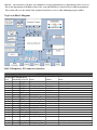
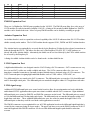
Logi-Pi User Guide
From ValentFx Wiki
LOGi Pi - Bringing FPGA Technology to the Raspberry Pi
Contents
1 Overview
1.1 Features
1.2 Peripherals
2 Electrical
3 Interfacing
3.1 Top Level Block Diagram
3.2 RA2.1 Raspberry Pi Connector Interface
3.3 PMOD Expansion Port
3.4 Arduino Expansion Port
3.5 LVDS Expansion Port
3.6 LVDS signal usage
3.7 Push Button Usage
3.8 DIP Switch Usage
3.9 LED Usage
3.10 JTAG Interface
4 Programming the FPGA from the Raspberry Pi
5 Raspberry Pi SPI to FPGA Interface
5.1 Direct SPI Communication to FPGA
5.2 SPI to Wishbone Interface Bandwidth
6 Useful Links
6.1 LOGi - Repository - Projects, Libraries, Drivers
6.2 LOGi-Pi Schematics
6.3 LOGI-Pi User Guide -LOGi-Pi documentation
6.4 LOGi Projects wiki - LOGI and Users projects will be documented here
Overview
The LOGi-Pi is the first FPGA development platform that has been optimized for use with the Raspberry Pi. The
LOGi-Pi adds FPGA flexibility and capability that allows the Raspberry Pi to be easily morphed into endless digital
applications. The FPGA/CPU combination the LOGi-Pi creates an incredibly powerful and versatile digital canvas
for users to create their imaginative digital designs.
Features
FPGA: Spartan 6 LX9 – TQFP144 Package - XC6SLX9-2TQG144C
Plug and play interfacing the Raspberry Pi
Arduino Shield expansion allowing for more than 200 existing plug in hardware modules
PMOD compatible headers allowing for more than 50 existing low cost hardware modules
4 layer optimized design to support maximum performance of high bandwidth applications
Length tuned GPMC, SDRAM and LVDS signals for high performance applications
50 Mhz MEMS oscillator
Peripherals
2x Push buttons
2x DIP Switch
1x High bandwidth SATA connector expansion port
44 FPGA IO available through PMOD and Arduino headers
2x Digilent Inc. PMOD ports supporting 59+ plug and play hardware modules
1x Arduino Header supporting 200+ Arduino Shield modules
Optional I2C, SPI access from the Beaglebone
10x length matched LVDS pairs routed as: 100 ohm differential, 50 ohm single-ended
256 Mb SDRAM
Electrical
External Vin Connector
Voltage Max. Voltage Min.
6V
4V
The LOGi-Pi can be powered through the Raspberry Pi connector or from the on-board external power
connector. If powering the LOGi-Pi from the Raspberry Pi connector, it is recommended that a 1A external
power supply be used to power the Raspberry Pi. Most FPGA applications will not require the use of a separate
external power supply to power the LOGi-Pi, but it is up to to ensure that the FPGA applications will not overload the Raspberry Pi power rails which will cause brown-outs and or system failures.
All current LOGi applications can be run while being powered only from the Raspberry Pi connector. The user
should test newly designed applications to ensure the FPGA load falls within acceptable values. Information
relevant to the Raspberry Pi system power requirements can be found the Raspberry Pi wiki.
The LOGi-Pi uses LDO regulators to supply 3V3 and 1V2 to the onboard peripherals and the FPGA in order to
reduce costs. The power distribution was designed to allow maximum dissipated heat to the internal and external
power planes. If very high demand applications are designed testing should be done to ensure that the LDO
regulators are not overheated due to the heavy loads. All current applications have been tested including the heavy
load of the bitcoin mining applications and no over-heating issues have been found.
Interfacing
The LOGi-Pi was designed to allow for easy expansion to a maximum number of off-the-shelf hardware modules.
The LOGI-Pi uses Digilent Inc. PMOD expansion ports and an Arduino Shield expansion port that give users a
plug-and-play experience with over 250 off-the-shelf hardware modules. A SATA port was added to board to be
used for maximum bandwidth applications. There are 10 LVDS pairs routed on the board that are all length
matched. These interfaces will allow for a multitude of varying applications to be implemented on the LOGi-Pi.
Due to the high amount of flexibility of the board, some pin functions are shared between different peripherals.
This section will cover the details of the peripherals and how to use to while eliminating any pin conflicts.
Top Level Block Diagram
RA2.1 Raspberry Pi Connector Interface
Pi-FPGA-ARDUINO Shared Pins
Default
Raspberry Pin State Raspberry
PI IO
Raspbian Pi Function FPGA
Arduino
Notes
1
3V3_RP
NC
2
5V_RP
Powers LOGi-Pi
3
GPI - HiZ RP_SDA
FPGA_SDA_GPIO
ARD_SDA
FPGA or Pi can access
4
5V_RP
Powers LOGi-Pi
5
GPI - HiZ RP_SCL
FPGA_SCL_GPIO
ARD_SCL
FPGA or Pi can access
6
GND
7
GPI - HiZ GPIO_GCLK FPGA_GPIO
8
GPI - HiZ RP_TX
FPGA_GPIO_RX
ARD_Master_RXFPGA or Pi can access
9
GND
10
GPI - HiZ RP_RX
FPGA_GPIO_TX
ARD_Master_TX FPGA or Pi can access
11
GPI - HiZ GPIO_GEN0 FPGA_MODE0_GPIO
12
GPI - HiZ GPIO_GEN1 FPGA_MODE1_GPIO
13
GPI - HiZ GPIO_GEN2 FPGA_GPIO
14
GND
15
GPI - HiZ GPIO_GEN3 FPGA_GPIO
16
GPI - HiZ GPIO_GEN4 FPGA_INITB_GPIO
17
3V3_RP
18
19
GPI - HiZ GPIO_GEN5 FPGA_PROGB
GPI - HiZ SPI_MOSI FPGA_MOSI_GPIO
the Arduino I2C Port
the Arduino I2C Port
the Arduino Uart Port
the Arduino Uart Port
FPGA pin cannot be used as GPIO (Reset)
20
21
22
23
24
25
26
GND
GPI - HiZ SPI_MISO FPGA_MISO_GPIO
GPI - HiZ GPIO_GEN6 FPGA_DONE
GPI - HiZ GPIO_SCLK FPGA_SCK_GPIO
GPI - HiZ SPI_CE0N FPGA
GND
GPI - HiZ SPI_CE1N FPGA_GPIO
FPGA pin cannot be used as GPIO
PMOD Expansion Port
There are 4 x Digilent Inc. PMOD ports populated on the LOGi-Pi. The PMOD ports allow for a wide array of
COTS modules to easily be interfaced with the LOGi-Pi. A listing of all currently available Digilent Inc. PMOD
modules can be found on their site. More 3rd party PMOD modules can be found by searching on google.
Arduino Expansion Port
An Arduino header is used to expand the on-board capability of the LOGI-Pi with more than 200 COTS arduino
shields currently on the market. The LOGi-Pi arduino header supports UNO, DUEM and DUE Arduino headers.
The Arduino header can optionally be accessed directly by the Raspberry Pi either by direct shared connections or
indirectly through the FPGA. This allows for direct use of the Raspberry Pi's SPI, I2C, UART hardware to
directly talk to the Arduino shields. Alternatively the shields can be accessed directly by the FPGA which can then
be accessed by the Raspberry Pi.
A listing of available Arduino shields can be be found on the Arduino shield list site.
LVDS Expansion Port
A high bandwidth interface was designed onto the LOGi-Pi using a SATA connector. SATA connectors are very
low cost and SATA cables are readily available and cheap. The SATA connector allows for a low cost
impedance controlled connection to externally designed modules that are designed using a SATA connector. The
LOGi Team anticipates designing high bandwidth modules such as LVDS camera, LVDS ADC, etc.
Two differential pairs are routed to the SATA connector. The differential pairs are routed as 100 ohm differential
and 50 ohm single ended pairs. The differential pairs are matched in length to within .015" length from each other.
LVDS signal usage
Additional LVDS differential pairs were routed on the board to allow for experimentation and work with further
multi-channel LVDS applications that require more than is available with the SATA connector. Eight additional
differential pairs were routed to PMOD3 and PMOD4 connectors on the board. The differential pairs are routed
as 100 ohm differential and 50 ohm single ended pairs. The differential pairs are matched in length to within .015"
length from each other. These additional differential pairs were also routed to match the length of the SATA
differential pairs so that they could be used in the same applications as needed.
The PMOD connectors are not optimized for use in LVDS application based on the differential signal length the is
created by the connectors being 90 degree angles. The upper and lower rows on the PMOD connector do NOT
match in length and if the PMOD connector is to be used this differential length in path should be taken into
account.
The PMOD connectors are not optimal for differential signals as they are not capable of maintaining the differential
impedance based on the large separation of the signal throughout the length of the connector. It is possible to
minimize this mismatch by replacing the PMOD connectors with low profile .100" vertical headers that will shorten
the path of separation therefore minimizing the impedance mismatch and allow for higher bandwidth interfaces. For
optimal performance using the LVDS signals on PMOD3 and PMOD4 it is recommended that LVDS signals be
directly soldered to the header pads to eliminate the impedance mismatch that occurs throughout the connector.
Push Button Usage
Two push button switches are provided on the LOGi-Pi. The pushbuttons are configured active high and an
discrete 10k ohm pull-up resistor is populated on-board to eliminate the need for configuring and used the on-chip
pull-up resistors. Additionally a DNP capacitor footprint is provided to allow users to install a capacitor for analog
debounce functionality. It is recommended the soft debounce logic be used in HDL, if the debounce functionality is
not enable by use of an installed capacitor,
DIP Switch Usage
A two position DIP switch is used on the LOGi-Pi. It is anticipated that the DIP switch be used for mode control
and other general purpose usage.
LED Usage
Two general purpose LED's are used on the LOGi-Pi. Due to the limited pin availability on the FPGA TQFP
package the LED pins are also shared with two rarely used PWM inputs on the Arduino Shield (RA2.1 only).
JTAG Interface
A unpopulated JTAG header is available on the LOGi-Pi. The JTAG header is contains the Digilent Inc. 6 pin
function pinout and is a .100" 6 pin header. The Digilent Inc JTAG adapters or xinlinx flying lead adapters can be
used to interface with the FPGA through the JTAG connection. The JTAG connection allows for direct
programming FPGA or onboard Flash memory, additionally chipscope can be used for deep debug and analysis.
Programming the FPGA from the Raspberry Pi
The main method of programming the FPGA is to use the LOGi Loader from the Raspberry Pi. The LOGi Loader
is a a program that has been developed to automate the process of loading the FPGA. The user needs to
download the LOGi Loader from the LOGi github repository and install the loader application on the Raspberry Pi
device. Once installed, the LOGi Loader can be invoked from the location of the stored FPGA bit file. The LOGi
loader will load the FPGA with the given bitstream file.
Raspberry Pi SPI to FPGA Interface
The Raspberry Pi to FPGA main communication interface is the PI SPI port. The Max Theoritical SPI clock rate
support on the Pi is "NEEDED VALUE". Though, based our development experience there are some instability
issues that can occur when reaching very high clock rates. The current LOGI drivers implement a 32Mhz clock
reliably. With further work users may be able to increase this clock rate with further driver deveopment.
Direct SPI Communication to FPGA
With the current 32Mhz clk and direct communication to the FPGA the user can expect to get 4 MB/S throughput
between the Raspberry Pi and the FPGA.
SPI to Wishbone Interface Bandwidth
When using the LOGI wishbone interface architecture the there is 16 bits of communication overhead. This leads
to the a maximum theoretical throughput of 3.8MB/S. In practice we have consitently gotten above 3 MB/S.
Useful Links
LOGi - Repository - Projects, Libraries, Drivers
LOGi - Repository
LOGi-Pi Schematics
LOGi-Pi Schematics
LOGI-Pi User Guide -LOGi-Pi documentation
LOGI-Pi User Guide
LOGi Projects wiki - LOGI and Users projects will be documented
here
LOGi Projects wiki
Retrieved from "http://valentfx.com/wiki/index.php?title=Logi-Pi_User_Guide&oldid=670"
Category: Logi-Pi
This page was last modified on 1 May 2014, at 10:12.
This page has been accessed 7,598 times.