1
The Service Processor Subsystem of the
StarT-Voyager Network of Workstations
by
0O
Brad J. Bartley
Submitted to the Department of Electrical Engineering and
Computer Science
in partial fulfillment of the requirements for the degree of
Master of Engineering in Electrical Engineering and Computer
Science
at the
MASSACHUSETTS INSTITUTE OF TECHNOLOGY
June 1997
@ Massachusetts Institute of Technology 1997. All rights reserved.
7
Author
Department of ectrical Engineeri
I
Certified by.-. ......
I
and Computer Science
May 20, 1997
4
....... .....
......................... ..
George A. Boughton
Principal Research Engineer
Thesis Supervisor
Accepted by .............
...........................
Arthur C. Smith
Chairman, Departmental Committee on Graduate Theses
2 997
The Service Processor Subsystem of the StarT-Voyager Network of Workstations
by
Brad J. Bartley
S.B. Electrical Science and Engineering (1996)
Massachusetts Institute of Technology
Submitted to the
Department of Electrical Engineering and Computer Science
May 20, 1997
In Partial Fulfillment of the Requirements for the Degree of Master of Engineering in
Electrical Engineering and Computer Science
ABSTRACT
StarT-Voyager is a network of workstations being designed and built by the Computation
Structures Group at the Laboratory for Computer Science. Voyager is an effort to create a
high-performance message-passing/shared-memory multiprocessor economically by
leveraging off commodity workstations and operating systems. Cache-coherence is
maintained by programmable protocols running on a support processor (sP) on the network
endpoint system (NES) of each node. This thesis details the design of the sP subsystem of
the NES.
Thesis Supervisor: George A. Boughton
Title: Principal Research Engineer
Chapter 0 Introduction
Voyager Overview
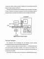
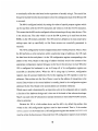
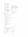
StarT-Voyager is a Cluster Area Network (ClAN) Parallel System [2] being designed
and built by the Computation Structures Group at the Laboratory for Computer Science.
StarT-Voyager is an effort to make a parallel computer by connecting many desktop class
SMP (symmetric multi-processor) machines, specifically IBM RS/6000 Model 240's. By
replacing one of the processors in each SMP with a network endpoint system (NES) each
node of the CIAN (see Figure 1) can be very tightly coupled to the network without
redesigning the whole SMP. This tight coupling to the network and minimal modification
to each node should permit StarT-Voyager to achieve good performance, while keeping both
the cost of each node and the cost of development low.
StarT-Voyager is to be a hybrid shared-memory message-passing machine. Voyager's
message passing is to be very aggressive, providing packets of various sizes and extremely
low latency, particularly for small packets [3]. Minimum latency for a 4 byte packet, for
instance, is expected to be near one microsecond, end to end. Additionally, Voyager's
memory sharing protocol is to be completely programmable.
The final remarkable feature of StarT-Voyager is the use of Arctic, a home-grown high
performance (320 Mbyte/s) network fabric particularly well suited to the low-overhead,
low-latency demands of a shared memory system. [4]
Related Work
Both message-passing and shared-memory architectures are represented in commercial
systems, but hybrid architectures are found primarily in academic projects. These hybrid
architectures have been explored in several projects. Notable examples include the MIT
Alewife Machine [1] and the Stanford FLASH Multiprocessor [8].
Of these, StarT-Voyager is most like FLASH and its dedicated protocol processor. Both
intend to build low-overhead shared memory onto message passing. However, FLASH relies
/ Ilocal RAiJ
I
aEi
NES
to Arctic
erview
heavily on custom hardware, including a custom I/O controller. Voyager is different in that
it leverages as much as possible off of off-the-shelf technology. Using commodity
workstations as nodes running a commodity operating system should make the cost of the
StarT-Voyager project comparatively low, while coupling the NES directly to each node's
memory bus (an unusual approach in low-cost systems) should provide quite good
performance.
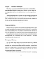
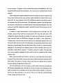
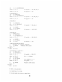
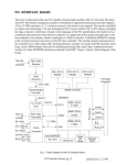
The sP Subsystem
The part of the NES which will execute the shared-memory protocol is the support
processor (sP) subsystem. The sP is a full-fledged off the shelf microprocessor, a PowerPC
604 just like the application processor (aP) where user code runs. Because the sP is a
completely general processor, implementing a new shared memory protocol is simply a
software matter.
The sP requires in its subsystem many features typical to stand-alone computers.
Non-volatile storage is required for initialization code which is run when the subsystem is
powered up. A large amount of RAM (32 megabytes) is needed to hold operating code and
protocol state. A level-two cache is not necessary but can significantly improve performance
in some cases. Finally, a memory controller is needed to serve as an interface between the
sP and its various memories. (see Figure 2)
The design of this sP subsystem and its initialization code is the subject of this thesis.
The task is essentially in three parts: development of the tools and techniques needed for
subsequent design work, design of the initialization code, and design of the hardware.
sP subsystem
I
I
I
I
I
I
I
i
to aP
I
I
I
I
I
to Arctic
Figure 2Network Endpoint System
Tools and Techniques
The infrastructure work of developing tools and techniques involved acquiring
development and analysis tools and developing working methods.
A critical tool in the early stages was an evaluation board, i.e., a working computer based
on the same processor and memory controller as was used in the sP subsystem. The
evaluation board permitted the testing of initialization and operating code long before our
own hardware was available.
Such testing on the evaluation board was facilitated by an IBM RISCWatch processor
probe. This device connects to the evaluation board via an IEEE 1149.1 (JTAG) debugging
port and gives the user complete access and control to the processor. The RISCWatch
processor probe will continue to be useful once our own hardware is constructed and must
be debugged.
Acquisition, configuration, and explication of these tools was critical in making the
design of the sP subsystem possible. We could not wait until our own hardware was
available to begin developing the boot code. The evaluation board made earlier development
possible. Additionally, debugging the hardware will be impossible without sophisticated
diagnostic equipment like RISCWatch.
In addition to this hardware, working methods had to be developed. Most notably, the
process for loading code onto the evaluation board or sP subsystem was an essential task but
one far from simple since we did not have the benefits of even a simple operating system on
the sP. A source program, written in C or assembly must be compiled or assembled with no
operating system calls. The resulting object file must then be converted into a file containing
pure machine code (called a binary). The binary must then be loaded onto the evaluation
board, either into RAM or into the board's ROMs. If the former, the binary must be loaded
via the processor probe. If the latter, the binary must be converted into a format suited to
PROM programming equipment.
Some of the tools for these steps existed and simply had to be found and learned. Other
tools had to be created. These are the tools with which initial ideas were evaluated and with
which actual systems will be tested.
Design of the Firmware
The second major component of this thesis is the design of the software which initializes
the sP subsystem when the machine is powered on or reset: the boot code.
This code must initialize both the 604 processor and memory controller, which have
many optional features and programmable parameters. The boot code's final task upon
execution is to load the shared-memory protocol code from the aP side of the node, and
transfer control to that code. Implementation of this task in a flexible and maintainable
fashion required a clear specification of the interface between the firmware and the code the
firmware loads.
The design of the firmware began with the component specifications and a single
example of initialization code for the memory controller. The user's manuals of the
PowerPC 604 [11] and memory controller [10] were especially critical in this stage.
A significant difference between software and hardware design is that creating a
defective piece of software is not particularly costly. Many generations of the boot code
were created and tested on the evaluation board at comparatively little expense in effort or
time. This ability permitted the cautious design strategy of initially developing very simple
code and subsequently adding functionality and re-testing the code at every step.
Since StarT-Voyager is a research machine, modifications to the software are likely. To
accommodate changes, the firmware was structured simply and documented thoroughly.
Design of the Hardware
The final major component of this thesis is the design of the hardware of the sP
subsystem.
The sP must be able to execute arbitrary cache-coherent-shared-memory protocols. That
is, it must be nearly a fully functioning computer in itself. Additionally, the sP must support
IEEE 1149.1 so that it can be probed and tested like the evaluation board.
The method followed was to select those components which were not already specified,
acquire documentation of all of the components (and examples of their use in whole systems,
in some cases) and to derive from that information a suitable system. Specifications which
turned out to be critical were those for the PowerPC 604, the memory controller chip, and
the RISCWatch processor probe. Electrical as well as architectural characteristics of several
components had to be taken into account, so hardware specifications were used in addition
to the user's manuals.
Additionally, there were design considerations beyond functional correctness. Because
the design of the NES is ambitious and the board will be physically limited to a small
form-factor, component count was kept low in the design of the sP subsystem.
The end result of the design of the hardware is code written in the Verilog hardware
description language which can be converted into a netlist. A netlist is a file describing
which pins of which components are to be connected via traces on the printed circuit board.
This netlist will be combined with a netlist for the rest of the NES board and sent to a private
company which will design the physical layout of components and fabricate the board. Since
some signals may be sensitive to electrical noise, close work with board manufacturer will
be necessary in the layout stage.
The sP subsystem of StarT-Voyager is intended to be both powerful and general. It is
very nearly a computer unto itself, and this thesis encompasses all aspects of that
subsystem, from the laying of groundwork and tool acquisition, through implementation
of early code to run on the subsystem, to design of the physical aspects of the subsystem.
Chapter 1 Tools and Techniques
When I began my association with the StarT-Voyager project, my responsibilities
were clear: to specify precisely the design of the sP subsystem. Little else was laid out.
A working method would have to be established as there was no clear cut procedure to
follow.
The plan which developed was to first make a few high level design decisions such as
precisely which models of processor and memory controller to use. With those decisions
made, development tools could be chosen and then with some sense of the capabilities of
the tools, a software and hardware design plan could be laid out.
Component Selection
Based on conservative evaluations of how obtainable both technical information (which
was needed immediately) and the components themselves (which would be needed in short
order, but not immediately) were, it was decided to use the PowerPC 604 rather than the
newer 604e and similarly to use the MPC105 memory controller rather than the MPC106.
Choosing the primary components early allowed me to begin acquiring documentation.
Becoming familiar with the components and the overall architecture of the system
constituted most of the early project work.
Development Hardware
After I had become roughly familiar with the PowerPC604 and the MPC105 memory
controller, I was in a position to begin evaluating various options for development
equipment. After much effort to find detailed technical specifications, we were able to
acquire both an example system on which software could be developed even before our own
system was working and a compatible hardware debugger which would make software
development on the example system possible.
The example system was a Motorola Atlas motherboard (intended for use in desktop
workstations) which is based on the 604 and 105 and (very significantly) supports access to
the processor via an IEEE 1149.1 (JTAG) port. Being based on the same primary
components meant that most of the initialization software which would be used in the sP
subsystem could also be run on Atlas. Supporting JTAG meant that the Atlas board could
be easily controlled and detailed reports of its state (including register, cache, and memory
contents) recorded.
The hardware debugger was an IBM RISCWatch system available as a beta release at
the time we acquired it. RISCWatch allows many operations to be performed on the target
system including reading and writing into memory, executing code in memory (a single
instruction at a time if desired), and viewing the contents of all processor registers. All of
this could be achieved by use of a simple graphical interface. Furthermore, RISCWatch
provides the ability to automate these operations by writing command scripts.
Simply acquiring the tools was not enough, however. Though both the Atlas board and
RISCWatch support IEEE1149.1 (JTAG), the physical connection could not be made until
the Atlas board had a suitable connector soldered to it. Additionally, much effort was
invested in configuring the RISCWatch hardware and installing the software. These efforts
resulted in a mostly working suite of tools, though it turns out that Atlas and RISCWatch are
not entirely compatible. Modifications to Atlas to fix the incompatibility are possible but
were deemed too difficult to implement so the ability to reset Atlas from RISCWatch simply
had to be done without. The consequence of this incompatibility is that when Atlas is reset,
RISCWatch continues to display information retrieved before the reset. [7] If the user is
careful to manually reload important information after an Atlas reset, the problem is
alleviated.
So once it was clear what the tools would do the plan became to write simple code, and
increase its functionality, testing on Atlas at each step.
Code Development Tools
With the hardware infrastructure in place and working, techniques used throughout the
project could begin to be developed. A way to make Atlas (and later our own hardware)
startup with our own program had to be found. That is, our program had to be placed in the
boot ROMs of Atlas.
Since most of the initialization work consists of placing specific values in specific
special purpose registers, programming in assembly language was most suited to the task.
The goal then, was to find a way to take assembly code and put the corresponding directly
executable machine code on a programmable ROM which could be plugged directly into
Atlas (and later our own hardware). It is from these ROMs that the Atlas's processor takes
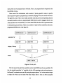
its instructions upon powerup. There are a number of steps between assembly code and a
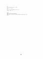
programmed ROM device. (See figure 3).
assembly source 1
assembler "as'
assemblysource2
I1
re I-I
object file 1
-
-
assembly source n
I
object file 2
objcopy -0binary
binary 1
-
1
binary 2
object file n
I1
binary n
ahxcat
ASCII
Hex file
Figure 3 Code path
The first step in the path from assembly code to boot ROM must be an assembler. For
this, the standard assembler "as" supplied with the AIX operating system and running on a
lab PowerPC workstation was used. By using the proper options, "as" can be made to output
an object file which can be linked with other object files to form an AIX executable
program. An object file, however, contains much information which is operating system (and
linking) related and therefore extraneous to the purposes of the boot code writer. The object
file, then, must be converted into something more usable.
The gnu utility "objcopy" is well suited to the task. "objcopy" is intended to convert
object files of any one of many formats into any other of those formats. "objcopy" also has
the option, however, of outputting a straight binary version of the object file input. Using this
option removes all operating system and linkage information from the code and leaves only
a sequence of opcodes which map exactly to the instructions in the original assembly source
file. The resulting binary file contains exactly the information that is needed on the ROM.
Binary files can be loaded into the RAM of Atlas via RISCWatch. In some cases where
ROM devices could not be programmed this method was used. Loading into RAM, however,
could not be our only testing method since access to RAM is possible only after the Atlas
board has booted. When testing our own boot code, therefore, we could not place the code
in RAM and be sure it was running under the same conditions it would encounter if run
immediately from ROM upon system reset.
A binary file, however, is not readable by the ROM programming equipment. It must be
put into a format which can be read by the ROM programmer.
Formats readable by ROM programming equipment are rather arcane, which meant that
an off-the-shelf conversion solution could not be found. Fortunately, most ROM formats are
also rather simple. With reference to definitions of various prospective file formats [5] I
could choose a format for which writing a conversion program would be simple and which
would also provide the ability to position sections of code in various places within the ROM.
(The latter ability being critical for placing specific blocks of code at specific addresses,
exception vectors most notably.) The format which best met the requirements was the
"ASCII Hex with STX" format. Implementing a C program to convert from straight binary
to ASCII Hex was a straightforward matter.
The original binary to ASCII Hex conversion program was a quick first pass intended
only to verify proper understanding of the output format. It was called "bin2ahx". "bin2ahx"
only worked with files with specific names and had to be modified and recompiled every
time a new section of code needed to be placed at a different address within the ROM.
"bin2ahx" sufficed in the testing stages but a more flexible solution would be needed. A tool
which would not require an understanding of the underlying C code would allow team
members other than the author to easily make modifications to the boot code. So a more
general tool called "ahxcat" (since it concatenates various input files into a single ASCII
Hex file) was written. (For the source code to "ahxcat" which includes a description of the
program's use, see Appendix A.) "ahxcat" allows its user to specify on the command line
which input files to use and where to place them in the ROM. "ahxcat" outputs its results
to standard output, allowing the user to redirect the output into any file or into additional
processing.
With "ahxcat" the path is complete. A developer can write several assembly code files,
run the assembler on each one, run "objcopy" on each resulting object file, and run "ahxcat"
to condense all of the binary files into a single ROM file. This process is simple and
methodical, but tedious and missing a step can cause much lost time in the debugging
process. To alleviate these problems, the UNIX utility "make" was used to automate the
process and make sure all necessary steps in the process are taken when a change to a source
file is made. A discussion of the "make" utility can be found in numerous widely available
sources. The makefile used for this project can be found in Appendix B.
PROM Programming
Trouble remained with the debugging process. Even though each step of the process
outlined above worked correctly, and the end result was a valid ASCII Hex file which was
accepted by the ROM programmer, the programmer would not accept the devices (AMD
29F040 FlashROMs). After replacing various parts of the ROM programmer to no avail, we
became suspicious that we had been using a batch of defective devices. Our suspicions were
confirmed when the programmer manufacturer sent us a device of the same model which
they had been able to program and which we too successfully programmed. More devices
of that type were ordered, but they too were found unprogrammable. Much of the software
development work was achieved with that single usable device. It was later discovered that
a similar model of device (AMD 29F0 10) could be programmed reliably with our equipment
15
and could be used in Atlas, though they hold only one fourth as much data as the original
device.
Additional developments also revealed that the devices we had previously believed
defective could in fact be programmed reliably when other models of ROM programmers
were used. Much time and effort was spent resolving these issues, but persistent use of the
tools and working devices available always allowed for some progress.
The equipment and techniques described above represent a complete set of tools for
developing boot code. And while the initial focus of this section of work was tool
development, code development always proceeded as well. Whenever the equipment or
techniques were used, it was done so with actual code intended to someday be part of the sP
boot sequence. At a certain point, however, the tools became stable and the techniques
complete. At this point efforts could be entirely devoted to boot code development.
Chapter 2 Boot Code
In any system which is more than trivially sophisticated, power up or reset is not simply
a matter of turning on power. Each of the sP and the 105 Memory Controller has a
significant amount of state information which must be set properly for the specific
configuration found in the sP subsystem. This state controls what features of the sP are
enabled and how the memory controller will attempt to access the DRAM which serves as
main memory and the SRAM which serves as level two (L2) cache, among many other
options.
In addition to setting this state every time the system is powered on or reset, the sP
subsystem must in some way respond to the application processor (aP). Exactly how the sP
responds, however, must be easily changed if the benefit of a fully programmable protocol
processor is to be realized and if the system is to allow its users to evaluate multiple cache
coherence protocols. The code that the sP subsystem executes on every reset must be very
general, then, and not do anything which the system software designers might wish to
change.
It is the firmware stored in the boot ROMs which must ensure that the configuration state
in all components of the sP subsystem are set properly and that the subsystem is capable of
interacting with the rest of the NES. Furthermore, the firmware must be clearly documented
so that any necessary modifications can be made without expending effort learning
unnecessary details of the sP subsystem components. Finally, it was useful when the
firmware was being written to verify methods for performing certain low-level operations
such as enabling address translation which the system software designers might wish to use.
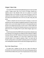
Boot Code: General Issues
The method used to implement the boot code was to begin with nothing but
documentation, that is manuals and specifications of the components being programmed (the
PowerPC 604 and the Motorola 105), and to write a first approximation of the code, and then
to continually refine the code based on the experience of actually using it. The crucial first
thing to be learned from the documentation is how the configuration state of the 604 and 105
is accessed.
The 604 is configured entirely by setting the values of special purpose registers which
can be read from with the MFSPR instruction and written to with the MTSPR instruction.
This means that the 604 can be configured without interacting with any other devices. (This
is not strictly true. The code which is run on the 604 at power up is read from the boot
ROMs via the 105 memory controller. The 105, however, defaults to its most conservative
settings upon start up specifically so that those accesses are essentially guaranteed to
succeed.)
The 105 is configured by memory mapped interactions with the processor. That is, when
the 604 performs a write instruction within a particular range of addresses, the 105 reads
the data from the bus and places it in the 105 configuration register corresponding to the
address of the write. Reads to that range of address similarly result in the contents of the
appropriate configuration register being put on the bus for the processor to read. When the
105 is configured (in hardware) to use its B map, all of its configuration registers are
accessible as described above. When the 105 is using map A, however, configuration
registers must be accessed indirectly [10]. In this mapping, the 105 responds to only two
addresses. Data written into the first of these is used as the address of transactions to the
second. Data written to the second address is actually placed in the configuration register
addressed by the first. Reads to the second address are similarly redirected.
Which map is used is determined by an input into a pin on the component and so is purely
a function of the hardware design and is thus out of the hands of the software developer.
Map A was used in the sP subsystem to maintain similarity to most other PowerPC systems,
Atlas in particular.
Because the 105 is a little-endian device and the 604 is by default big-endian, data
written to the 105 configuration registers must be byte-reversed. That is, if the number
OxO 0 112 2 3 3 is to be written into a 105 configuration register the number 0x3 3 2 2110 0
must be written by the processor. Data read from 105 configuration registers must similarly
18
be byte-reversed. In practice, the byte-reversals are usually accomplished by use of the
special PowerPC load and store instructions 1wbrx and s twbrx (load/store byte-reversed
indexed).
These configuration registers establish what kind of memory devices are attached to the
105 as main memory and L2 cache, and how quickly operations on those devices can be
performed. The exact meaning of each 105 configuration register is beyond the scope of
this document. See [10] for more details. The configuration registers of the 604 determine
what features of the processor are enabled and how certain operations take place. The exact
meaning of each 604 configuration register is beyond the scope of this document. See [11]
for more details.
In addition to simple documentation, several examples proved invaluable. The [10]
includes a section of boot code from an actual system. The values this code writes to 105
configuration registers provided an example of a typical use of that device. And once the
Atlas evaluation board and RISCWatch debugger (see Chapter 1) were operational, a
working system could be booted and the contents of its configuration registers both in the
105 and the 604 could be viewed. This information was particularly helpful since the sP
subsystem is derived largely from the Atlas board. Finally, the form of a correct assembly
language file was determined by compiling simple C code to assembly (rather than to an
executable or object file) by using the "-S" option on a typical C compiler. The output then
was a correct assembly language file which could be used as a template for hand written
assembly code.
When code had actually been written, it could be run on the Atlas board and its effects
reviewed. If the code resulted in an error, the source could be found and a correction to the
code written. This process of writing, testing, and fixing was repeated until all desired
functions had been implemented without errors.
All of the initialization, with one exception, could be tested in this way even before an
NES had been assembled. Since Atlas has no L2 cache, that part of the initialization code
could be written but not evaluated until an actual NES becomes available. At that time,
however, the same procedure as was used on Atlas can be followed: iterating through
writing, testing, and fixing the code.
Boot Code: Voyager Specifics
604 Initialization
What the boot code must achieve was at first only vaguely specified. Certain tasks are
clearly necessary, such as enabling access to main memory. Other tasks were similarly
obvious, such as the enabling of the level 1 caches of the 604 and enabling superscalar
operation of the 604. More precise specifications of the boot code requirements were later
provided in an unofficial document from the Voyager system architects (see Appendix C).
For the most part, the individual requirements are simply implemented. Enabling the
level 1 data cache (D cache), for instance, is simply a matter of setting two bits in the 604
HIDO (Hardware Implementation-Dependent) register simultaneously. Since the two bits
are in the same register, a single MTSPR (move to special purpose register) instruction can
set both at once. One of the bits enables the register while the other causes the cache to be
emptied of any potentially incorrect data. The clearing operation only works if the cache is
enabled, so the clear bit should not be set before the enable bit. Also, it is dangerous to have
the cache enabled before it has been emptied because in the interim a data access could result
in incorrect data being read from the cache and used. Enabling and clearing the cache
simultaneously is simpler than trying to ensure that no data accesses (or exceptions which
might cause data accesses) occur between the enabling and the clearing.
The situation is very similar in the case of the instruction cache (I cache), except that the
simultaneous setting of enable and clearing bits is even more essential. Instruction accesses
cannot be avoided (because the program must continue to run) so the danger of reading
incorrect instructions from the cache is more difficult to avoid.
Enabling the superscalar operation of the 604 is simply a matter of setting a single bit
in the HIDO register.
Address translation, while not part of the sP boot requirement, will be useful in the
system software so the method for enabling translation was also learned and here
documented. Full-fledged address translation is complicated and beyond the scope of this
work, so the simplest form of address translation was used. The PowerPC architecture
20
specifies the existence of a Block Address Translation (BAT) mechanism. In the BAT
scheme, if an untranslated (real) address falls within a range of addresses specified in the
BAT registers, the translated address will be simply the offset of the real address within the
range added to a different base address. Each mapping of ranges within the BAT scheme
comes with several protection and access mode bits, including a bit to indicate if accesses
to that range are to be "guarded". [9] (If a region of memory is marked "guarded" it indicates
that that memory does not behave as deterministically as normal memory. Memory mapped
I/O devices are the most typical example.) For instruction BATs the "guarded" bit is
reserved and must not be set, despite indications that instruction accesses made without
address translation treat the "guarded" bit as set. Attempting to set the "guarded" bit in an
instruction BAT will result in protection violations when accesses are attempted.
Furthermore, the order in which BAT registers are updated is important. The information
governing a single BAT mapping is stored in two registers, so all of the information cannot
be changed in a single instruction. One of those register contains a valid bit which indicates
whether the information in those two registers should be used in address translation. So
when a BAT mapping is being turned on, the register containing the valid bit should not be
set until the other register has been, otherwise there will be a brief time when the valid bit
indicates that translations can proceed, but the second register does not yet hold valid data.
Conversely, when a BAT mapping is being turned off, the register containing the valid bit
should be changedfirst.
105 Initialization
The state of the 105 controls numerous options and, most notably, the timing
characteristics of the DRAM used as main memory and of the SRAM used as level two
cache. Since the sP subsystem uses DRAM identical to Atlas, the DRAM timing parameters
can be copied directly from Atlas. (This is done as Atlas runs, via the RISCWatch debugger.)
However, since Atlas has no level two cache, the SRAM timing parameters must be
determined directly from the specifications of the particular devices chosen to implement
the L2 cache. Testing of the L2 cache initialization cannot occur until an NES is fabricated.
When the timing parameters are set, and certain delays are held to allow the DRAM to
initialize itself, the bits in the 105 which permit main memory and L2 cache access can be
set. Clearing of the L2 cache before enabling is handled in the hardware of the cache.
Loading System Code
While it is important that the state of the sP subsystem be clearly specified so that system
software can rely on that state, a method for loading system code into the sP by way of the
aP is even more critical. Without such a mechanism, new code can be loaded into the sP
subsystem only by physically replacing the ROMs on the NES.
The informal document in Appendix C specifies a protocol by which new system code
can be loaded into the sP subsystem upon every reset. This protocol provides a mechanism
by which the aP can send data to the sP subsystem where it will be placed in main memory.
As a final step in the protocol, control of the sP is handed over to code which had been
copied over from the aP. In this way the aP can specify precisely what the sP does after
initialization, thus minimizing the requirements placed on the sP firmware, which is
relatively difficult to change.
The protocol relies on certain memories accessible to both the aP and the sP. (see Figure
2) Since nothing like that memory exists on Atlas, testing of the protocol code, like the L2
initialization code, must wait until an NES has been fabricated. The code which implements
the aP to sP protocol is in Appendix F.
Source Code
The assembly code which performs the sP subsystem initialization and interfaces with
the system software can be found in Appendices D, E, and F. The aP to sP protocol code is
separate for logical reasons. The initialization code is separated into two files because of the
layout of PowerPC exception vectors. The reset exception code is to be located at address
OxFFF00 10 0 and the machine check exception code is to be located at OxFFFO0 2 0 0, so
if the reset exception code extends beyond 256 bytes (i.e., 64 instructions since each
instruction is four bytes long) a machine check exception would cause the processor to jump
22
into the middle of the initialization code. The actual code which is placed at the reset
exception vector, then, must be no more than 64 instructions long and the rest must be placed
away from all other exception vectors. The code at the reset exception vector must branch
to the code away from the exception vectors.
All of the sP subsystem initialization/startup requirements have been implemented in
assembly code. With the exception of L2 cache initialization and the aP to sP protocol, all
of the code has been successfully tested on the Atlas evaluation board. Given the similarity
of the sP subsystem to Atlas, we are confident that that code will successfully initialize an
NES. And due to the simplicity of the parts as yet untested, we believe that as they stand or
after only minor fixes, they too will operate correctly.
23
Chapter 3 Hardware
The sP subsystem must meet several requirements. To perform its function it must be
able to execute any arbitrary cache coherence protocol and it must do so with enough speed
to avoid becoming a performance bottleneck. Cache coherence protocols generally rely on
large directories of information, so the sP subsystem must have a large main memory.
In addition to these functional requirements, the sP subsystem, being a physically
implemented system, must meet several physical criteria. First, it and the rest of the NES
must fit within the space available in the case of the node computer. Second, it must
dissipate heat away from the components (most notably the PowerPC 604) rapidly enough
to keep the components within the operating temperature range.
Finally, the sP subsystem, if there is to be any hope of making it work, must provide
some method by which it can be debugged. For this reason the sP must have a test access
port compatible with the RISCWatch hardware debugger.
Starting Point
The design process began with several specifications handed down by the system
architects. These decisions were based on rough assessments of required performance and
included which processor to use at what speed, which model of memory controller to use,
and how much main memory the sP subsystem must have. With these decisions made, the
appropriate evaluation board could be chosen and documentation could be acquired. The
documentation included the User's Manuals and Hardware Specifications of the PowerPC
604 [11] and the 105 memory controller [10] and complete schematics of the Atlas
evaluation board.
Due to the simplicity of the sP subsystem and its similarity to Atlas, the design could be
largely derived from that for Atlas. Design of the level two (L2) cache, however, could not
be derived from Atlas so components had to be selected and their appropriate connectivity
determined.
24
From the start, the design of the sP subsystem was intended to be simple and to adhere
as closely as possible to that for Atlas, which was known to work. In most cases within the
design where various options existed, the option used in Atlas was chosen.
Component Selection
The processor and memory controller choice was essentially made by the system
architects, though some decisions such as not using the 604e or the 106 memory controller
due to uncertain part availability were made during sP subsystem design.
Choosing what kind of DRAM to use as sP subsystem main memory was also an easy
decision. Using standard DRAM SIMMs meant that the sP subsystem would vary little from
the known to work design (Atlas) and that suitable DRAM would be both easily and cheaply
available.
Choosing which read only memory devices to use to hold the sP subsystem's boot code
was a similarly simple decision. For a time when programming the type of device used on
Atlas was not possible, other devices were considered, but once the programming problem
was resolved by using a lower density device of the same family, the choice was again
obvious.
Since Atlas has no L2 cache, there were no obvious component choices for this part of
the subsystem. To implement an L2 cache, there must be data devices for holding the cached
data and a tag device for holding address information for each line of data in the data
devices. The primary characteristic of these devices is capacity and disposition of that
capacity. The data devices, for instance, must hold 64 bits on each address (since this is the
width of the data bus). And since the total size of the L2 cache as specified by the system
architects is 512k bytes, the number of addresses (the "depth") in the devices must be
512k bytes / 8 bytes = 64k addresses.
No single device is available in that configuration, but combinations of two or four
devices can be shaped properly. Two 64k deep by 32 bit wide devices or four 32k deep by
32 bit wide devices would both be appropriate. To reduce component count on the board to
save space, two device solutions were given priority. Also, since combining devices in width
25
is more straightforward than combining them in depth (In the former case, all devices are
always active. In the latter case, one set of devices or the other is active, depending on the
address.), 32k deep devices were not considered. In the end, a device at 64k by 32 bits
designed specifically for use as L2 cache in PowerPC systems was found, the Motorola
63P63 1.Many other manufacturers offer very similar if not identical devices, but availability
determined the choice of the Motorola part.
Similar size calculations are made for the tag device. The tag must have an address for
each cache line. Since cache lines are 32 bytes and the cache is 512k bytes in size there must
be
512k bytes / 32 bytes = 16k lines
in the cache and therefore 16k addresses in the tag. (Size of a cache line does not equal the
size of an addressable location in the data devices. Loading a cache line requires four bus
transactions or a single burst-of-four transaction.)
The width of the tags which the tag device must hold must also be determined. 32 bits
are required to distinguish any given byte in memory. Since the cache is direct mapped, the
location of a given byte of data within the cache implies a certain number of bits of the
address of that byte. The tag must resolve the remaining bits of address. Since there are 512k
bytes in the cache and it takes 19 bits to address 512k locations (219 = 512k), 32 - 19 = 13
bits must be resolved by the tag. [12]
Only a single model of device, the Motorola 27T416, was found to be of the proper depth
and hold large enough tags. Fortunately this device was also designed for use in PowerPC
systems.
Unfortunately this device actually holds 14 bits of tag. Having capacity to spare seems
like a blessing rather than a burden, but that extra bit must be treated very carefully. The tag
device sometimes compares stored tags with portions of the address currently on the bus.
Whatever signal is input to that extra bit must not differ from the bit stored by the tag device
or it will not recognize a match. The simplest solution then, is for that bit to always receive
the same signal and to always store the value corresponding to that signal. This can be
achieved by attaching the input to ground via a resistor. The resistor must have a high
enough resistance that when the tag device outputs a signal, the current drawn will not
exceed the rating of the device. Furthermore, the resistor must have a low enough resistance
that the voltage on the pin can be drained off between when the pin functions as an output
and when it functions as an input again. Because the tag should never output any value it has
not previously read (which should only ever be zero for that bit), the worst cases should
never occur so an error in choosing the pull down resistance should not cause an error. A
robust design, however, will work even if the worst does happen.
Determining Connectivity
Once all of the components were chosen, precisely how they were to be connected on
the NES board had to be determined and specified to the board fabricator.
Connectivity Derived Directly from Atlas
The most sophisticated devices in the sP subsystem are the processor itself and the
memory controller. These share numerous signals, but their clearly defined roles leave few
options for how the two should be connected. The connectivity between these two devices
came directly from the Atlas design.
The connectivity of the DRAM sockets could also come largely from Atlas. But where
Atlas had 4 sockets, the sP subsystem has only two to save board space. (This decision also
took into account the amount of memory which can be supported by 2 sockets and how
much memory might be required by the software running on the sP.) Fortunately, the second
pair of DRAM sockets on Atlas could simply be omitted from the sP subsystem. All signals
connected to those sockets were determined to suffer no ill effects from being connected to
nothing. This was mostly obvious from the fact that Atlas works correctly with its second
pair of DRAM sockets empty.
The connectivity of many minor components including glue logic, buffers and
termination resistors on the DRAM was derived directly from Atlas.
Since the size of the boot code is quite small and would easily fit within a single ROM,
one of the ROM sockets could have been omitted from the sP subsystem, but the space
27
savings would have been small so the sP subsystem design adheres to that of Atlas and has
two ROM sockets.
Level two cache components
Since Atlas is not equipped with built-in level 2 cache, no complete references were
available. However, partial information was available from both the 105 User's Manual [10]
in the form of a rough example of an L2 cache implementation and from the tag device and
data device data sheets. Analysis of the meaning of specific signals on the cache devices
allowed a specific version of the generic example to be devised. The precise connections
between the sP subsystem bus, the 105, and the cache devices are illustrated in Figure 4.
Several features of these connections are remarkable.
First, note that the MATCH output from the tag device is not used, since it is an active
high signal and the 105 expects an active low signal. The _TA output of the tag device can
be used as an active low version of MATCH. (see MPC27T416 data sheet)
Also note the pull-up resistor on the TV output of the 105, which is necessary because
that output is of the open collector type so it cannot go high. This resistance must be chosen
so that it will not draw too much current from the 105 but so that it can still pull up the signal
to the tag device within a cycle of the 105's clock.
Also note the disposition of the signal TDQO on the tag device. This pull-down ensures
that that bit will never prevent an otherwise correct match from occurring.
Finally, a deviation from the Atlas design is apparent. The 105 has outputs which may
be optionally used to indicate which individual byte within a cache line is to be written to.
[10] These outputs are the Data Write Enables (DWEO - DWE7). If they are not used, logic
outside of the 105 must determine from the transfer size and address on the bus which byte
write enables on the L2 cache should be set. On Atlas, the DWE signals are not used. The
two options available then, were to either create the external byte write decode logic, or to
enable the DWE signals available from the 105. The former was not available from the
Atlas schematics and the latter would deviate from the Atlas design. In the end, enabling the
105's DWE signals was simpler and reduced the number of components required in the sP
60x bus
AO-A31
105
tag
device
memory
controller
A13- A26
goAO -A12
1 AO - A13
WT
_TWE
t :
TOE
to 60x bus TT1*--
TV
DIRTYOUT
HIT
-1
~---
40
--
·------
>
----------
>
~
I-
DIRTYIN
N.C. 4N.C. 4-
WS
GT
GS
TT1
VALIDD
DIRTYD
TA
TDQ1 - TDQ13
TDQ0O
DIRTYQ
VALIDQ
MATCH
data
devices
A13 - A28
>
TALE
_ADS
i71
_BAA
DOE
DWE0 - _DWE7
60x bus
DO-D63
! !
.
t
AO - A15
CE
_ADSC
ADSP
ADV
BWE
_OE
_BW1-_BW3,
BW1-_BW3
GW
DQ1 DQ32,
DQ1 - DQ32
Figure 4 L2 cache connectivity
subsystem.
JTAG
The JTAG port is a connector to which the RISCWatch hardware debugger may be
29
board soft
board hard
04)
ESET
ESET
ST
ESET
ST
Figure 5 RISCWatch and reset signals
attached. The connector should be connected to the sP subsystem in such a way that the
subsystem will work properly whether or not a debugger is attached. This means that when
no debugger is attached, no spurious signals must come from the connector, so all signals
coming from the connector to the rest of the subsystem must be pulled to either power or
ground, as appropriate for each signal. But when a debugger is attached, those pull-ups and
pull-downs must not cause the signals which come from the debugger to be affected.
Because of reported errors with the JTAG interface of the Atlas board, reference to that
design was avoided. Fortunately, clear specifications of how each signal should be held are
provided in the RISCWatch User's Guide, Appendix A [7]. These specifications were
followed except in the case of the _TRST signal. As specified in the RISCWatch User's
Guide, that signal should be pulled up but the 604 User's Manual [11, section 8.10.1] says
that _TRST "should be held asserted during normal operation", so a pull down was used
instead. See Figure 5.
30
Reset
Since the sP subsystem is not a system unto itself, it relies on some board level signals
from other parts of the system. Among these are the hard and soft reset signals and clock
signals. Resetting the proper devices under the proper conditions requires some glue logic.
The desired reset behavior is for all devices supporting hard reset to do so whenever
either the board hard reset signal or the RISCWatch hard reset signal is asserted, and for the
604 to soft reset when either the board soft reset signal or RISCWatch soft reset signal is
asserted. The logic required to achieve this behavior consists simply of several logic-AND
gates (since reset signals are active low). The configuration of the JTAG port and reset
signals is shown in Figure 5.
Decoupling Capacitors
Some devices, notably complicated integrated circuits like microprocessors, are both
sensitive to variations in power supply voltage and can cause variations, potentially
disrupting other devices. To prevent such problems it is good practice to place capacitors of
various values connected from power to ground near some of the power inputs of such
devices.
The 604 Hardware Specification makes the rigorous recommendation that one of these
decoupling capacitors be placed on each power pin of the 604. That suggestion was followed
closely. The 105 Hardware Specification suggests a only single decoupling capacitor. To be
conservative, several decoupling capacitors were placed on the 105.
PCI Bus Truncation
The sP subsystem is in some respects simply the subset of the Atlas board which is
connected directly to that system's 60x memory bus. That is, the sP subsystem lacks Atlas's
PCI (peripheral component interconnect) bus and everything attached to it. The Atlas PCI
bus is attached to the 60x bus by way of the 105. Since nothing is attached to the PCI bus
in the sP subsystem, the PCI connection on the 105 must be wired such that it appears to the
105 as if no PCI transactions ever take place. This wiring was a simple matter of placing pull
down resistors on the PCI data and address signals and pulling PCI control signals (and 105
specific PCI sideband signals) to their inactive states. [6, 10]
Process
The design of the hardware is specified in a Verilog hardware description language file.
The Verilog code is a structural model of the system being described. That is, the code
represents how the various components are connected to each other, but contains no
information about what the components actually do. A tool developed within the
StarT-Voyager project is used to convert the Verilog representation of the design into a
netlist in a format acceptable by the board fabrication company.
Before the net list can be created, however, the sP subsystem Verilog code must be
combined with code for the rest of the system. Upon completion, the sP subsystem code was
handed off to be integrated into the system as a whole. That code for the NES as a whole will
then be converted into a net list to be given to the board fabricator.
The hardware is to be constructed (the board layed out, fabricated, and components
attached) by an outside firm specializing in such work and based on the netlist of our
specification. In addition to the netlist, however, the fabricator must also follow a list of
layout notes which specify, for instance, which devices must be physically close together on
the board, which signal traces must be short in length, and which signal traces should not
come close to each other.
Since the layout notes are an informal document, close work with the board fabricator
will be required to ensure that the requirements are understood and implemented.
While use of standard components in a standard design leaves little room for variation,
much work is involved in specifying in detail a system of this complexity. Real world
concerns such as part availability compound the situation. Fortunately, most decisions could
be resolved by some simple criterion such as adherence to the known design or minimizing
32
part count.
Initially, the sP subsystem will be integrated into a slow speed prototype of the NES.
This prototype will allow us to evaluate the correctness of both the sP subsystem and the rest
of the system and give a chance before the actual system is built to make design revisions,
should they be necessary.
Careful design and extensive reference to known working systems means that such a
revision will likely be unnecessary. We expect the system to function correctly in its initial
version.
Chapter 4 Conclusion
Integration
All three major parts of the sP subsystem project, the tools and techniques for
development, the firmware, and the hardware, are done. The tools and techniques allowed
the design parts of the project to proceed and will facilitate both further design revisions and
debugging of the existing design. The software necessary for writing firmware and moving
it to ROMs suitable for the sP subsystem, including an assembler, an object file converter,
and several custom programs are in place and the procedures for using them are clearly
documented. An evaluation board is in place for testing firmware until the NES hardware
is available. The RISCWatch hardware for debugging the evaluation board and the NESs is
in place and configured.
The firmware necessary to make the sP subsystem work is complete and documented.
The code which performs device initialization is written and tested. The code which
communicates with the aP to load and run the cache coherence code is written. Additionally,
code demonstrating the use of address translation in the sP is written, tested, and
documented.
The hardware design is complete. The sP supports execution of any arbitrary code either
from the firmware in ROMs or as loaded from the aP. Directory data structures of very large
size can be constructed in the sP's DRAM. The sP subsystem is ready to be integrated into
the rest of the NES. In short, the sP subsystem is capable of running any specified cache
coherence protocol.
With the completion of these three parts, the sP subsystem is ready for whatever may
come next. If hardware or firmware design revisions need be made, the tools to do so are in
place. If all that remains is construction, the designs and the tools for debugging are in place.
What Could be Done Differently
In the end it was clear that much of the work in the project was, while not precisely
productive, necessary for learning. So even though much of that work would not be repeated
34
if the project were to be undertaken again, it cannot be viewed as wasted effort.
Other decisions which were made turned out to be needlessly conservative but were the
proper decisions given the information available at the time. Most notable among those were
the decisions to use the PowerPC 604 rather than the 604e. The decision was made to use
the lower performance 604 because that model was shipping at the time and there were no
guarantees that the 604e would be available in time for our needs. For similar reasons the
decision was made to use the 105 memory controller rather than the more sophisticated, but
later arriving, 106.
Redesigning the hardware to incorporate these higher performance devices would likely
be a simple matter, but one too time consuming to be undertaken in this final stage of the
StarT-Voyager project. Additionally, rewriting the software to support the 106 could be quite
tedious and there would be no way to test it short of building an NES or acquiring a new
evaluation board to use as the Atlas board was used. (Incorporating the 604e in place of the
604 should not require any substantial software changes, as the two are nearly identical at
the programming level of abstraction.)
For these reasons and the shortness of time, the sP subsystem is unlikely to be redesigned
even though these simple changes could improve the performance of StarT-Voyager as a
whole. At some point design must stop and construction begin.
Comparisons with Objectives
Despite not being as fast as it could be, the sP subsystem is done.
The design of a system which can execute arbitrary cache coherence code and which can
be incorporated into an NES tightly coupled to an off-the-shelf workstation exists. The boot
code for the system is written and the tools and techniques for debugging are in place.
All that was set out to be done, has been done.
Future Directions
While the code which runs on the sP will change greatly during the life of the
StarT-Voyager system (that's why the sP is fully programmable after all), the sP itself is
35
unlikely to change much in future versions of the system. Indeed, given the expense of
physically constructing a system the hardware of the NES is unlikely ever to be revised.
The firmware, however, can be updated quite easily and cheaply. It seems likely then,
that the boot code will grow in sophistication as it becomes more clear what the system must
do. Code which diagnoses potential problems within the sP subsystem, the NES, or even
within the cluster as a whole seems a probable addition to the current bare minimum code.
Final Word
With the finalization of the sP subsystem, an important and clearly identifiable part of
the StarT-Voyager machine is complete and ready for integration into the system.
Acknowledgements
For their knowledge, patience, and humor, I would like to thank Andy Boughton, Mike
Ehrlich, and Boon S. Ang. For advice on and off the topic of work, I thank Jack Costanza.
It was joy to work with Chris Conley, Dan Rosenband, and Handong Wu.
My parents Francis and Janice gave me what I needed and trusted my judgement on what
to do with it. They think nothing of it, but I know now how important that trust is.
Without Curtis, I wouldn't have made it to MIT. May I make as much difference for
Bryan Andrew.
I thank Bud and Mary for the opportunity and the unabashed encouragement.
36
References
[1]
A. Agarwal, R. Bianchini, D. Chaiken, K. L. Johnson, D. Kranz, J.
Kubiatowicz, B.-H. Lim, K. Mackenzie, and D. Yeung. The MIT Alewife
Machine: Architecture and Performance. In Proceedings of the 22nd Annual
InternationalSymposium on ComputerArchitecture, pages 2 - 13, 1995.
[2]
B. S. Ang and D. Chiou. StarT-Voyager*. In Proceedingsof the MIT
Student Workshop for Scalable Computing, 1996.
[3]
B. S. Ang, D. Chiou, L. Rudolph, and Arvind. Message Passing Support
in StarT-Voyager. MIT Laboratory for Computer Science, CSG Memo 387,
July 1996.
[4]
G. Boughton. Arctic Routing Chip. MIT Laboratory for Computer
Science, CSG Memo 373, April, 1995, In Proceedingsof the 1994
University of Washington ParallelComputer Routing and Communication
Workshop, May, 1994.
[5]
Data I/O Corporation. Unisite Universal Programmer User Manual. May
1991.
[6]
Intel Corporation. PCI System Design Guide, revision 1.0. 8 Sept.
1993.
[7]
International Business Machines Corporation. RISCWatch Debugger User's
Guide. 1996.
[8]
J. Kuskin, D. Ofelt, M. Heinrich, J. Heinlein, R. Simoni, K.
Gharachorloo, J. Chaplin, D. Nakahira, J. Baxter, M. Horowitz, A.
Gupta, M. Rosenblum, and J. Hennessy. The Stanford FLASH
Multiprocessor. In Proceedingsof the 21st Annual International
Symposium on Computer Architecture, Chicago, II, Apr. 1994.
[9]
Motorola Incorporated. PowerPC Microprocessor Family: The Programming
Environments. 1994.
[10]
Motorola Incorporated. MPC105 PCI Bridge Memory Controller User's
Manual. 1994.
[11]
Motorola Incorporated. PowerPC 604 RISC Microprocessor User's Manual.
1994.
[12]
S. Ward and R. Halstead. Computation Structures. MIT Press, 1990.
37
Appendix A
"ahxcat" source code.
ahxcat.c
This will take an arbitrary number of straight binaries (as produced
by "objcopy -0 binary ...
" and concatenate them into a single
ASCII Hex with STX file suitable for use on the PROM burner.
Syntax is:
ahxcat [ Zxxxx I binfilen ]*
That is, any combination of filenames indicating binaries or address
directives (a 'Z' followed by 4 hex digits). An address directive
causes the next binary file to be placed at that address. Consecutive
files (ie, those without address directives between them) will simply
be concatenated.
Output is to stdout.
With no arguments, prints a syntax summary.
This code is derived largely from bin2promAHX.c.
History:
31 Jan 1997
created - bbartley
#include <stdio.h>
#define STX 2
#define ETX 3
void printbyte(FILE *fp, int ch);
int checksum; /* Yeah, yeah, it's a global variable. */
main(int argc, char **argv) {
FILE *in;
FILE *out;
int arg;
int addr;
int c;
if (argc == 1) { /* no command line arguments given */
fprintf(stderr, "Usage: \n%s [ Zxxxx I binfilen ]* \n\n ", argv[01);
binaries\
fprintf(stderr, "That is, any combination of filenames indicating
or address\n directives (a 'Z' followed by 4 hex digits). An address\
directive\n causes the next binary file to be placed at that address.\
them)\
Consecutive\n files (ie, those without address directives between
will simply\n be concatenated.\n");
exit(0);
}
checksum = 0;
out = stdout;
/** HEADER **/
fputc(STX, out);
/** BODY **/
for (arg = 1; arg < argc; arg++) {/*iterate through command line args
if (*argv[arg] == 'Z')
{
*/
/* this arg is an address directive */
/* sscanf(argv[arg] + 1, "%x", &addr); */
fprintf(out, "\n$A%s,\n", argv[arg]+l );
} else {
/* this arg is a bin file */
in = fopen(argv[arg], "r");
if (in == NULL) {
fprintf(stderr, "Couldn't open: %s
I else { /* dump the file */
while ((c = fgetc(in))
printbyte(out, c);
Continuing\n", argv[arg]);
!= EOF) {
fclose(in);
}
} /* for */
/** TRAILER **/
fputc(ETX, out); /* print ETX */
fprintf(ouL, "\n$S%04X,\n", checksum % Ox10000); /* keep checksum to 4
*/
/* don't close out since it is stdout */
exit(0);
} /* main */
void printbyte(FILE *fp, int ch) {
checksum += ch;
fprintf(fp, "%02X ", ch);
}
dig
Appendix B
Boot code makfile.
all: BootL.ahx
# Smoosh all the binaries into a PROM file
It
BootL.ahx: InitA.bin InitB.bin PEV.bin Prot.bin ahxcat
./ahxcat Z0100 InitA.bin Z0200 PEV.bin Z0300 PEV.bin Z0400 PEV.bin Z0500 PEV.bin Z0600
PEV.bin Z0700 PEV.bin Z0800 PEV.bin Z0900 PEV.bin ZOA00 PEV.bin ZOBOO PEV.bin ZOCOO PEV.bin
ZOD00 PEV.bin ZOEOO PEV.bin Z3000 InitB.bin Prot.bin > BootL.ahx
# Make the binary to PROM file converter
#t
ahxcat: ahxcat.c
gcc -o ahxcat ahxcat.c
# Turn object code into straight binaries.
It
InitA.bin: InitA.o
/map/sys/gnu/bin/objcopy -0 binary --set-start=0xfff00100 InitA.o InitA.bin
InitB.bin: InitB.o
/map/sys/gnu/bin/objcopy -0 binary --set-start=0xfff03000 InitB.o InitB.bin
PEV.bin: PEV.o
/map/sys/gnu/bin/objcopy -0 binary --set-start=0xfff00700 PEV.o PEV.bin
Prot.bin: Prot.o
/map/sys/gnu/bin/objcopy -0 binary Prot.o Prot.bin
# Turn assembly code into object files.
InitA.o: InitA.s
as -o InitA.o InitA.s -i -m ppc
InitB.o: InitB.s
as -o InitB.o InitB.s -1 -m ppc
PEV.o: PEV.s
as -o PEV.o PEV.s -1
Prot.o: Prot.s
as -o Prot.o Prot.s -1
#t
40
clean:
rm *.o *.bin *.lst *.ahx
Appendix C
aP to sP protocol.
Jan 16, 97
(A) Memory based, boot-time coordination between aP and sP.
use a set of known location in NES SRAM as mailboxes for
communication between the aP and the sP. Let's call these
locations aP2sP and sP2aP. Probably the former will be in
sSRAM, and the latter in aSRAM.
The possible cmds from aP to sP are:
Nop
[will see later why this is here]
Load (NES_SRAM_addr, sP_DRAM_addr, sizeWords)
Jump (new_IP)
sP, upon boot-up,
initializes aP2sP to Empty
polls on aP2sP;
each time a cmd is received, sP clears aP2sP to Empty,
indicating to the aP that the cmd has been received.
If an actual reply is needed, it is sent to the aP through
sP2aP mailbox.
aP, when it is ready to initialize sP subsystem, does the
following:
initializes sP2aP to Empty
issues Nop cmd into aP2sP
polls on sP2aP until it is Empty again.
now the aP can issue real cmds to the sP. It will probably
be a sequence of:
* Load (nsal, sdal, nwl)
* Load (nsa2, sda2, nw2)
* Load (nsaN, sdaN, nwN)
* Jump (nIP)
NB: The initial NOP allows the aP and sP to synchronize. It
assumes nothing about the initial values of the sP2aP mailbox,
which can either be Empty, or non Empty, and the relative order
in which the sP initializes it to Empty, and aP issuing the Nop
cmd.
Proof:
case 1: sP initializes aP2sP to Empty
followed by aP issuing the Nop cmd.
Initial value of aP2sP does not matter.
sP will see the Nop, but since it is Nop, nothing is done.
aP will see that the Nop has been accepted by the sP.
case 2: aP issuing the Nop cmd.
followed by sP initializes aP2sP to Empty
Initial value of aP2sP does not matter.
sP will not see the Nop, but it clears it during its
initialization.
It appears to the aP that the sP has accepted the Nop.
In both cases, aP and sP end up in the same state, ready for
further cmds.
42
(B) sP
*
*
*
*
*
*
*
604's state after boot:
data parity checking disabled. [NES not supporting parity.]
address parity checking enabled. [NES not supporting parity.]
instruction cache disabled
data cache disabled
L2 cache disabled
instruction address translation disabled
data address translation disabled
(C) Hardware requirement:
* ability to access the further SRAM (aP accesses sSRAM, sP
accesses aSRAM) upon NES hardware reset. More precisely:
o aBIU/sBIU must be able to coordinate the transfer sequence
o aBIU/sBIU must be able to generate the Data Motion requests
and hand them to CTRL.
o Data Motion unit must work.
43
Appendix D
Code for reset exception.
# Pathla.s
#t
First experiment to delve into the path from assembly code to
PROM. This will do some very rudimentary initialization and then
go into a tight loop. W/ RISCWatch, I should be able to determine
if it is executing properly.
# bbartley - 25 Sept 1996
# Modifications:
#
9 Oct 1996 - divided Pathl.as into 2 sections. This section,
#
Pathla.s belongs at the reset vector (ie, Oxfff0_0100).
#
Pathlb.s belongs away from vectors at Oxfff0_3000.
#
18 Dec 1996 - put an infinite loop at the beginning of the code
#
as per suggestion of Nabil Rizk.
#
22 Jan 1997 - after various fixes, made this part of PATH3.
#
Removing startup loops and proceeding with enabling
#
superscalarity and caches.
## LOAD AT Oxfff0 0100
##
# Header stuff I stole from some compiled code.
.set rO,0; .set SP,1; .set RTOC,2; .set r3,3; .set r4,4
.set r5,5; .set r6,6; .set r7,7; .set r8,8; .set r9,9
.set r10,10; .set rll,ll; .set r12,12; .set r13,13; .set r14 ,14
.set r15,15; .set r16,16; .set r17,17; .set r18,18; .set r19 ,19
.set r20,20; .set r21,21; .set r22,22; .set r23,23; .set r24 ,24
.set r25,25; .set r26,26; .set r27,27; .set r28,28; .set r29 ,29
.set r30,30; .set r31,31
.set fpO,0; .set fpl,l; .set fp2,2; .set fp3,3; .set fp4,4
.set fp5,5; .set fp6,6; .set fp7,7; .set fp8,8; .set fp9,9
.set fpl0,10; .set fpll,ll; .set fp12,12; .set fp13,13; .set fpl4, 14
.set fp15,15; .set fpl6,16; .set fp17,17; .set fp18,18; .set fp19,19
set fp20,20; .set fp21,21; .set fp22,22; .set fp23,23; .set fp24,24
set fp25,25; .set fp26,26; .set fp27,27; .set fp28,28; .set fp29,29
set fp30,30; .set fp31,31
.set MQ,0; .set XER,1; .set FROM_RTCU,4; .set FROM_RTCL,5; .set FROM DEC,6
set LR,8; .set CTR,9; .set TID,17; .set DSISR,18; .set DAR,19; .set TORTCU,20
set TO_RTCL,21; .set TODEC,22; .set SDR_0,24; .set SDR_1,25; .set SRR_0,26
.set SRR_1,27
.set BO_dCTR_NZERO_AND_NOT,0; .set BO_dCTR_NZERO_AND_NOT_1,1
.set BO_dCTR_ZERO_AND_NOT,2; .set BO_dCTR_ZERO_ANDNOT_1,3
.set BOIFNOT,4; .set BOIF NOT_1,5; .set BOIFNOT_2,6
.set BO IF_NOT_3,7; .set BO_dCTR NZERO AND,8; .set BO dCTR NZERO AND_1,9
.set BO_dCTR_ZERO_AND,10; .set BO_dCTR_ZERO_AND_1,11; .set BO_IF,12
.set BO_IF_ 1,13; .set BOIF_2,14; .set BO_IF_3,15; .set BO dCTRNZERO,16
.set BOdCTRNZERO_1,17; .set BO_dCTR_ZERO,18; .set BOdCTRZERO_1,19
.set BO_ALWAYS,20; .set BO_ALWAYS_ 1,21; .set BO_ALWAYS_2,22
.set BO_ALWAYS_3,23; .set BO_dCTR_NZERO_8,24; .set BO_dCTR_NZERO_9,25
.set BO_dCTR_ZERO_8,26; .set BO_dCTR ZERO 9,27; .set BO_ALWAYS 8,28
.set BO_ALWAYS_9,29; .set BOALWAYS_10,30; .set BO_ALWAYS_11,31
.set CRO_LT,0; .set CRO_GT,1; .set CRO_EQ,2; .set CRO SO,3
.set CR1_FX,4; .set CR1_FEX,5; .set CR1_VX,6; .set CR1_OX,7
.set CR2_LT,8; .set CR2 GT,9; .set CR2_EQ,10; .set CR2_SO,11
44
.set
.set
.set
.set
.set
.set
CR3_LT, 12; .set CR3_GT,13; .set CR3_EQ,14;
CR4_LT, 16; .set CR4_GT,17; .set CR4_EQ,18;
CR5_LT, 20; .set CR5_GT,21; .set CR5 EQ,22;
CR6_LT, 24; .set CR6_GT,25; .set CR6_EQ,26;
CR7_LT, 28; .set CR7_GT,29; .set CR7 EQ,30;
TOLT,16; .set TO_GT,8; .set TO_EQ,4; .set
.set CR3 SO,15
.set CR4 SO,19
.set CR5 SO,23
.set CR6 SO,27
.set CR7_SO,31
TO_LLT,2; .set TOLGT,1
# plus a little
.set rl,l; .set r2,2;
# associate names w/ SPRs
.set HID0,1008;
.set IBATOU,528;
.set IBATOL,529;
.set IBATlU,530;
.set IBATIL,531;
.set IBAT2U,532;
.set IBAT2L,533;
.set IBAT3U,534;
.set IBAT3L,535;
.set DBATOU,536;
.set DBATOL,537;
.set DBAT1U,538;
.set DBAT1L,539;
.set DBAT2U,540;
.set DBAT2L,541;
.set DBAT3U,542;
.set DBAT3L,543;
.set SDR1,25;
.set PMC1,953;
.set PMC2,954;
.set MMCR0,952;
.set SDA,959;
.set SIA,955;
# .set DAR,19;
# These are already defined above
# .set DSISR,18;
.set SPRGO,272;
.set SPRG1,273;
.set SPRG2,274;
.set SPRG3,275;
.set SRR0,26;
.set SRR1,27;
.set TBL,284;
.set TBU,285;
.set DEC,22;
.set IABR,1010;
.set DABR,1013;
# associate names w/ config addresses
.set EAGLE_REG,0x8000;
.set VEND_ID_REG,0x0000;
.set DEV IDREG,0x0002;
.set PCI_CMD,0x0004;
.set PCI_STAT,0x0006;
.set MEM_STA_03,0x0080;
.set MEM_STA_47,0x0084;
.set EXT_MEMSTA_03,0x0088;
.set EXT_MEM STA_47,0x008c;
.set MEM_END 03,0x0090;
.set MEM_END_47,0x0094;
.set EXT_MEMEND 03,0x0098;
.set EXT_MEM_END 47,0x009c;
45
.set
.set
.set
.set
.set
.set
.set
.set
.set
.set
.set
.set
.set
.set
.set
MEMBANK EN,0x00a0;
PROC CFGA8,0x00a8;
PROC_CFGAC,0x00ac;
ALT_OSV_I,0x00ba;
ALT_OSV 2,0x00bb;
ERR ENREG1,0x00c0;
MEM ERRD_REG,0x00cl;
CPU_BES REG,0x00c3;
ERR EN REG2,0x00c4;
ERR_DET REG2,0x00c5;
PCI BES_REG,0x00c7;
MEM_CFG_1,0x00f0;
MEM_CFG_2,0x00f4;
MEMCFG_3,0x00f8;
MEM_CFG_4,0x00fc;
#### NOTE:
#### Don't even try to understand this code without reading the 105 Manual,
#### chapter 3.
### This code should begin at Oxfff0_0100 (in memory space)
### (ie, 0x00100 in the ROM).
### After no more than 64 instructions, control should branch
### to a second block of code which should begin at Oxfff0 3000
### (ie, 0x03000 in the ROM).
start:
# set up registers w/ addresses
#
lis
rO, EAGLE_REG
ori
rl, rO, Ox0cf8
#
ori
r2, rO, Ox0cfc
#
# set PROM
lis
r3,
ori
r3,
stwbrx r3,
lwbrx
lis
ori
and
or
stwbrx
isync
r4,
rO,
rO,
r4,
r4,
r4,
of
rO
rl
r2
access points
= 0x8000_0000 base address
= 0x8000_0cf8 config address
= 0x8000_0cfc config data
access speed in 105
EAGLE_REG
# make a value which points to a
r3, MEMCFG_1
#
config register
0, rl
# make that register active
0, r2
0x0503
rO, 0x0002
r4, rO
r4, rO
0, r2
# r4 <- mem cfg register
#
#
#
#
# write modified data to CONFIG DATA
# not sure why. The Big Bend code does.
## 604 Config Registers
# on HRESET or SRESET, MSR should be set just right so
#
do nothing to it
# HIDO's reset value
#
and while I'm at
lis
r4, Ox0000
HIDO, r4
mtspr
mtspr
IABR,
nop #
mtspr
DABR,
nop #
is not clear, so make it all O's
it, make a bunch of others all 0 too.
r4
r4
# HIDO <-- OxO
# IABR <-- OxO
# DABR <-- OxO
46
# invalidate all the BATs
isync
mtspr
IBATOU, r4
IBATOL, r4
mtspr
mtspr
IBAT1U, r4
mtspr
IBAT1L, r4
mtspr
IBAT2U, r4
mtspr
IBAT2L, r4
mtspr
IBAT3U, r4
mtspr
IBAT3L, r4
DBATOU, r4
mtspr
mtspr
DBATOL, r4
mtspr
DBAT1U, r4
mtspr
DBAT1L, r4
mtspr
DBAT2U, r4
mtspr
DBAT2L, r4
mtspr
DBAT3U, r4
mtspr
DBAT3L, r4
isync
# Since not enabling address translation, TLBs and segment regs
#
(and SDR1) *should* be ok w/ out initialization
# disable IABR and DABR
nop #
mtspr
IABR, r4
nop #
mtspr
DABR, r4
# IABR <-- OxO
# DABR <-- OxO
# disable performance monitoring
lis
r4, Oxfa00
ori
r4, r4, Ox0000
mtspr
MMCRO, r4
isync
### !!! Branch to Oxfff0O3000, which is where Pathlb.s
###
should reside so as to avoid tromping on
###
exception vectors.
lis
r5, OxfffO
ori
r5, r5, 0x3000
mtspr
LR, r5
blrl
Appendix E
Boot code which is placed away from the reset exception vector.
# Pathlb.s
#
#
#
#
First experiment to delve into the path from assembly code to
PROM. This will do some very rudimentary initialization and then
go into a tight loop. W/ RISCWatch, I should be able to determine
if it is executing properly.
# bbartley - 25 Sept 1996
# Modifications:
#
9 Oct 1996 - divided Pathl.as into 2 sections. This section,
Pathlb.s belongs away from vectors at Oxfff0_3000.
#
#
Pathla.s belongs at the reset vector (ie, Oxfff0_0100).
#
10 Dec 1996 - incorporated some of the changes Boon recommended.
(His version is at /home/prj/StarT-voyager/sP-boot/Pathlb.s)
#
#
I think all but his last correction were correct.
#
22 Jan 1997 - after various fixes, made this part of PATH3.
Removing startup loops and proceeding with enabling
#
#
superscalarity and caches.
#
29 Jan 1997 - enabling address translation (using BATs only)
#
20 Feb 1997 - This version is now in AP2SP. Cleaning up the
experimental parts to leave just the initialization.
#
## LOAD AT Oxfff0_3000
##
Pathla.s will branch to this code.
# Header stuff I stole from some compiled code.
.set rO,0; .set SP,l; .set RTOC,2; .set r3,3; .set r4,4
.set r5,5; .set r6,6; .set r7,7; .set r8,8; .set r9,9
.set r10,10; .set rll,ll; .set r12,12; .set r13,13; .set r14,14
.set r15,15; .set r16,16; .set r17,17; .set r18,18; .set r19,19
.set r20,20; .set r21,21; .set r22,22; .set r23,23; .set r24,24
.set r25,25; .set r26,26; .set r27,27; .set r28,28; .set r29,29
.set r30,30; .set r31,31
.set fpO,0; .set fpl,l; .set fp2,2; .set fp3,3; .set fp4,4
.set fp5,5; .set fp6,6; .set fp7,7; .set fp8,8; .set fp9,9
.set fpl0,10; .set fpll,ll; .set fp12,12; .set fpl3,13; .set fp14,14
.set fp15,15; .set fp16,16; .set fp17,17; .set fp18,18; .set fp19,19
.set fp20,20; .set fp21,21; .set fp22,22; .set fp23,23; .set fp24,24
.set fp25,25; .set fp26,26; .set fp27,27; .set fp28,28; .set fp29,29
.set fp30,30; .set fp31,31
.set MQ,0; .set XER,1; .set FROM_RTCU,4; .set FROM_RTCL,5; .set FROM_DEC,6
.set LR,8; .set CTR,9; .set TID,17; .set DSISR,18; .set DAR,19; .set TO_RTCU,20
.set TO_RTCL,21; .set TO_DEC,22; .set SDR_0,24; .set SDR_1,25; .set SRR_0,26
.set SRR_1,27
.set BO_dCTR_NZERO_ANDNOT,0; .set BO_dCTRNZERO_AND_NOT_1,1
.set BO dCTRZERO AND NOT,2; .set BOdCTRZEROANDNOT_1,3
.set BO_IF NOT,4; .set BO_IF NOT_1,5; .set BO_IF NOT_2,6
.set BOIF NOT_3,7; .set BO_dCTR_NZEROAND,8; .set BOdCTR_NZEROAND_1,9
.set BO_dCTR_ZEROAND,10; .set BO_dCTR_ZERO_AND_1,11; .set BO_IF,12
.set BO_IF 1,13; .set BO_IF_2,14; .set BO_IF_3,15; .set BO_dCTR_NZERO,16
.set BOdCTR_NZERO_1,17; .set BO_dCTR_ZERO,18; .set BO_dCTRZERO01,19
.set
.set
.set
.set
.set
.set
.set
.set
.set
.set
.set
.set
.set
BO_ALWAYS,20; .set BO_ALWAYS_1,21; .set BO_ALWAYS_2,22
BO_ALWAYS_3,23; .set BO_dCTRNZERO_8,24; .set BOdCTRNZERO_9,25
BO_dCTR_ZERO_8,26;..set BO_dCTR_ZERO_9,27; .set BO_ALWAYS_8,28
BO_ALWAYS_9,29; .set BO_ALWAYS_10,30; .set BO_ALWAYS_11,31
CR0 LT,0; .set CRO_GT,1; .set CRO_EQ,2; .set CRO_SO,3
CR1_FX,4; .set CR1_FEX,5; .set CR1_VX,6; .set CR1_OX,7
CR2_LT,8; .set CR2_GT,9; .set CR2_EQ,10; .set CR2_SO,11
CR3_LT,12; .set CR3_GT,13; .set CR3_EQ,14; .set CR3_S0,15
CR4_LT,16; .set CR4_GT,17; .set CR4_EQ,18; .set CR4_SO,19
CR5_LT,20; .set CR5_GT,21; .set CR5_EQ,22; .set CR5_S0,23
CR6_LT,24; .set CR6_GT,25; .set CR6_EQ,26; .set CR6_SO,27
CR7_LT,28; .set CR7_GT,29; .set CR7_EQ,30; .set CR7_SO,31
TO_LT,16; .set TO_GT,8; .set TOEQ,4; .set TO_LLT,2; .set TOLGT,1
# plus a little
.set rl,l; .set r2,2;
# associate names w/ SPRs
.set HIDO,1008;
.set IBATOU,528;
.set IBATOL,529;
.set IBATlU,530;
.set IBATlL,531;
.set IBAT2U,532;
.set IBAT2L,533;
.set IBAT3U,534;
.set IBAT3L,535;
.set DBATOU,536;
.set DBATOL,537;
.set DBAT1U,538;
.set DBAT1L,539;
.set DBAT2U,540;
.set DBAT2L,541;
.set DBAT3U,542;
.set DBAT3L,543;
.set SDR1,25;
.set PMC1,953;
.set PMC2,954;
.set MMCRO,952;
.set SDA,959;
.set SIA,955;
# .set DAR,19;
# These are already defined above
# .set DSISR,18;
.set SPRGO,272;
.set SPRG1,273;
.set SPRG2,274;
.set SPRG3,275;
.set SRRO,26;
.set SRR1,27;
.set TBL,284;
.set TBU,285;
.set DEC,22;
.set IABR,1010;
.set DABR,1013;
# associate names w/ config addresses
.set EAGLEREG,0x8000;
.set VENDID_REG,0x0000;
.set DEV_ID_REG,0x0002;
.set PCI_CMD,0x0004;
.set PCISTAT,0x0006;
.set MEMSTA_03,0x0080;
.set MEM_STA_47,0x0084;
.se .t EXT_MEM_STA_03,0x0088;
.set EXT_MEM_STA_47,0x008c;
.set MEM_END_03,0x0090;
.set MEM_END_47,0x0094;
.se*t EXT_MEM_END_03,0x0098;
.set EXT_MEM_END_47,0x009c;
.set MEM_BANK EN,0x00a0;
.set PROC CFGA8,0x00a8;
.set PROCCFGAC,0x00ac;
.set ALTOSV_, 0x00ba;
.set ALT_OSV_2,0x00bb;
.set ERR EN REG1,0x00c0;
.set MEM_ERRD_REG,0x00cl;
.set CPU_BES_REG,0x00c3;
.se t ERR EN REG2,0x00c4;
.set ERR_DETREG2,0x00c5;
.set PCI_BESREG,0x00c7;
.set MEM_CFG1, 0x00f0;
.se t MEM_CFG_2,OxOOf4;
.set MEMCFG 3,0x00f8;
.se t MEM_CFG_4,0x00fc;
105 Config Registers
# power management resets to disabled, so don't mess w/ it
# disable all PCI stuff
lis
r3, EAGLEREG
ori
r3, r3, PCI_CMD
stwbrx r3, 0, rl
#
#
#
lis
r4, 0x0000
stwbrx r4, 0, r2
lhbrx
r4, 0, r2
li
r4, 0x0000
sthbrx r4, 0, r2
# clear
lis
ori
stwbrx
all
r3,
r3,
r3,
PCI stat bits
EAGLEREG
r3, PCI_STAT
0, rl
stwbrx
li
lhbrx
stwbrx
r4,
r3,
r4,
r4,
0, r2
Ox0002
r3, r2
r3, r2
# cfg_addr <-- PCI_CMD
# cfg_data <-- OxO
# r4 <-- cfg_data (for reference during debugging)
# cfgdata <-- OxO
# cfg_addr <-- PCI_STAT
# cfg_data <-- OxO
# clears all PCI_STAT bits
isync
# PROCCFGAC (PICR2)
lis
ori
stwbrx
r3, EAGLEREG
r3, r3, PROCCFGAC
r3, 0, rl
lwbrx
lis
ori
r4, 0, r2
rO, Oxae9e
r0O,rO, Oxed0e
# cfg_addr <-- PROCCFGAC
# r4 <-- cfg_data
and
lis
ori
or
stwbrx
r4,
rO,
rO,
r4,
r4,
lwbrx
lis
ori
or
stwbrx
r4, rO
Ox829e
rO, 0x650e
r4, rO
0, r2
# cfg_data <-- Ox a29e 650e
0, r2
Ox4000
rO, Ox0000
r4, rO
0, r2
# this block sets the L2 ENable
#
bit, but is not the final
#
enabling word. See PROC_CFGA8
#
below
# cfg_data <-- Ox c29e 650e
# PROCCFG A8
#
note that this does NOT enable L2
lis
r3, EAGLE_REG
ori
r3, r3, PROC CFGA8
stwbrx r3, 0, rl
# cfg_addr <-- PROC_CFG_A8
Oxff37
r4, Ox2e8c
0, r2
lis
ori
stwbrx
# r4 <-- Oxff372e8c
# cfg_data <-- r4
# ALTOSV_1
#
don't need to use this
# ALT OSV 2
#
don't need to use this
# ERR EN REG1
#
can leave this set to reset value
# MEMERRDREG
#
can leave this as reset
# CPU BES REG
#
can be left as reset
# ERR EN REG2
#
can be left as reset
# ERR_DETREG2
#
can be left as reset
# PCI BES REG
#
can be left as reset
isync
# MEMCFG 1
#
this one was set at the very beginning
# MEM CFG 2
#
note the REFINT should be 1562 cycles
lis
r3, EAGLE_REG
ori
r3, r3, MEM CFG 2
stwbrx r3, 0, rl
# cfg addr <-- MEM CFG 2
lis
ori
stwbrx
r4, OxO000
r4, r4, OxOfb7
r4, 0, r2
# MEM CFG 3
# r4 <-- Ox0000fb7
# cfg_data <-- r4
lis
ori
stwbrx
r3, EAGLEREG
r3, r3, MEM_CFG_3
r3, 0, rl
# cfg_addr <-- MEMCFG_3
lis
ori
stwbrx
r4, 0x0002
r4, r4, 0x3313
r4, 0, r2
# r4 <-- 0x00023313
# cfg_data <-- r4
# MEM CFG 4
lis
r3, EAGLEREG
ori
r3, r3, MEM_CFG_4
stwbrx r3, 0, rl
# cfg_addr <-- MEM_CFG_4
lis
ori
stwbrx
# r4 <-- Ox00100000
# cfg_data <-- r4
r4, Ox0010
r4, r4, Ox0000
r4, 0, r2
## Memory Bank Boundaries
most of these are going to be all Os, so...
##
lis
r4, Ox0000
# r4 <-- OxO
# MEMSTA_03
lis
r3, EAGLE_REG
ori
r3, r3, MEM_STA_03
stwbrx r3, 0, rl
# cfg_addr <-- MEM_STA_03
stwbrx r4, 0, r2
# cfg_data <-- OxO
# MEM STA 47
lis
r3, EAGLE_REG
ori
r3, r3, MEM_STA_47
stwbrx r3, 0, rl
# cfgaddr <-- MEM_STA_47
stwbrx r4, 0, r2
# cfg_data <-- OxO
# EXT MEM STA 03
lis
r3, EAGLE_REG
ori
r3, r3, EXTMEM_STA_03
stwbrx r3, 0, rl
# cfgaddr <-- EXT_MEM_STA_03
stwbrx
r4, 0, r2
# cfg_data <-- OxO
# EXT MEM STA 47
lis
r3, EAGLEREG
ori
r3, r3, EXT_MEM_STA_47
# cfgaddr <-- EXT_MEM_STA_47
stwbrx r3, 0, rl
stwbrx
r4, 0, r2
# cfg_data <-- OxO
# MEMEND_03
#
this is the only one that's not OxO, so do it at the
#
end
# MEMEND 47
r3, EAGLE_REG
lis
r3, r3, EXT MEMSTA_47
ori
# cfgaddr <-- EXT_MEM_STA_47
stwbrx r3, 0, rl
stwbrx r4, 0, r2
# cfg_data <-- OxO
# EXTMEM END_03
r3, EAGLE_REG
lis
52
ori
r3, r3, EXTMEMEND_03
stwbrx r3, 0, rl
# cfg_addr <-- EXTMEM_END_03
stwbrx
r4, 0, r2
# cfg data <-- OxO
# EXT MEM END_47
lis
r3, EAGLE_REG
ori
r3, r3, EXT MEM_END_47
stwbrx r3, 0, rl
# cfg_addr <-- EXTMEM_END_47
stwbrx
r4, 0, r2
# cfg_data <-- OxO
# MEM END 03
lis
r3, EAGLE_REG
ori
r3, r3, MEMEND_03
stwbrx r3, 0, rl
# cfg_addr <-- MEM_END 03
lis
ori
stwbrx
# cfgdata <-- 0x0000_001f
r4, Ox0000
r4, r4, Ox001f
r4, 0, r2
# MEM BANKEN
#
enable bank 0
lis
r3, EAGLE REG
ori
r3, r3, MEM_BANK_EN
stwbrx r3, 0, rl
# cfgaddr <-- MEM_ BANK_EN
lis
ori
stb
# cfg_data <-- Ox01
# DRAM
#
li
mtctr
wait100us:
bdnz
r4, Ox0000
r4, r4, Ox0001
r4, 0(r2)
configured and enabled
Must wait 100 us before accessing
rO, 0x2701
# decimal 10000 cycles
rO
waitl00us
# Set MEMGO
lis
r3,
ori
r3,
stwbrx r3,
bit in MEM CFG 1
EAGLE_REG
r3, MEM CFG_1
0, rl
lwbrx
lis
ori
or
stwbrx
0, r2
0x0008
rO, Ox0000
r4, rO
0, r2
li
mtctr
wait8ref:
bdnz
r4,
rO,
rO,
r4,
r4,
rO, 0x3000
rO
# cfg_addr <-- MEM CFG 1
# r4 <-- cfg_da ta
# set MEMGO bit in r4
# cfg_data <-- r4
# approx 12000 decimal
wait8ref
## DRAM is now available
# L2 enabling will go here.
## Do some reads and writes to memory here.
53
## (Leaving this in actual boot code because it could be
## a very important diagnostic.)
# write at the beginning of implemented memory space
lis
r4, 0x1234
ori
r4, r4, 0x5678 # make data 0x12345678
lis
r2, Ox0000
# make address OxO
stwx
r4, rO, r2
# put data at address
# write
lis
ori
stwx
in
r2,
r2,
r4,
the middle of the memory space
Ox0000
r2, Oxlllc # make address 0x0000111c
rO, r2
# write
lis
ori
lis
ori
stwx
at
r2,
r2,
r4,
r4,
r4,
the very end of the memory space
Ox01ff
r2, Oxfffc # make address Ox01ff_fffc
Ox9abc
r4, Oxdef0 # make data Ox9abc_def0
rO, r2
# do it
# read em back
lis
r2, Ox0000
lwzx
r10, rO, r2
# make address OxO
lis
ori
lwzx
r2, Ox0000
r2, r2, Oxlllc # make address Ox0000111c
r1l, rO, r2
lis
ori
lwzx
r2, Ox01ff
r2, r2, Oxfffc # make address Ox01ff_fffc
r12, rO, r2
### Engage D cache
# Enable D cache (so that clearing operation will work)
#
and clear the cache in one fell swoop
mfspr
r5, HIDO
ori
r5, r5, 0x4400 # set bit 17 and 21 (enable and clear)
mtspr
HIDO, r5
###
###
###
###
TEST D CACHE ENABLING
Removed this because it takes a human looking
at it to see if it worked.
END D CACHE TEST
### Engage I cache
# Enable I cache (so that clearing operation will work)
#
and clear the cache in one fell swoop
mfspr
r5, HIDO
ori
r5, r5, 0x8800 # set bit 16 and 20 (enable and clear)
mtspr
HIDO, r5
### Enable address translation
### (Actually, don't bother now. Leave that to later code.)
## Set superscalarity in HIDO
mfspr
ori
mtspr
r5, HIDO
r5, r5, 0x0080 # set bit 24
HIDO, r5
#### INITIALIZATION COMPLETE
#### Code following this should be what we came here to do.
####
55
Appendix F
Code which implements the sP side of the aP to sP protocol.
# Prot.s
# This is the code which implements the aP to sP boot protocol as
# specified in
# /tmp-mnt/home/prj/StarT-voyager/docs/sP-boot/sP-boot-spec-pO.text
# This code should immediately follow InitB
# bbartley - 20 Feb 1997
## TO FOLLOW InitB
# Header stuff I stole from some compiled code.
.set rO,0; .set SP,1; .set RTOC,2; .set r3,3; .set r4,4
.set r5,5; .set r6,6; .set r7,7; .set r8,8; .set r9,9
.set r10,10; .set rll,ll; .set r12,12; .set r13,13; .set r14,14
.set r15,15; .set r16,16; .set r17,17; .set r18,18; .set r19,19
.set r20,20; .set r21,21; .set r22,22; .set r23,23; .set r24,24
.set r25,25; .set r26,26; .set r27,27; .set r28,28; .set r29,29
.set r30,30; .set r31,31
.set fp0,0; .set fpl,1; .set fp2,2; .set fp3,3; .set fp4,4
.set fp5,5; .set fp6,6; .set fp7,7; .set fp8,8; .set fp9,9
.set fpl0,10; .set fpll,ll; .set fp12,12; .set fp13,13; .set fpl4,14
.set fp15,15; .set fpl6,16; .set fpl7,17; .set fpl8,18; .set fp19,19
.set fp20,20; .set fp21,21; .set fp22,22; .set fp23,23, .set fp24,24
.set fp25,25; .set fp26,26; .set fp27,27; .set fp28,28; .set fp29,29
.set fp30,30; .set fp31,31
.set MQ,0; .set XER,1; .set FROM_RTCU,4; .set FROM_RTCL,5; .set FROM_DEC,6
.set LR,8; .set CTR,9; .set TID,17; .set DSISR,18; .set DAR,19; .set TO_RTCU,20
.set TO_RTCL,21; .set TO_DEC,22; .set SDR_0,24; .set SDR_1,25; .set SRR_0,26
.set SRR_1,27
.set BO_dCTR_NZERO_ANDNOT,0; .set BO_dCTR_NZERO_ANDNOT 1,1
.set BO_dCTR_ZERO_AND_NOT,2; .set BO_dCTR_ZERO_AND_NOT_1,3
.set BOIF_NOT,4; .set BO_IF_NOT_ 1,5; .set BO_IF_NOT 2,6
.set BOIF NOT_3,7; .set BO_dCTR_NZERO_AND,8; .set BO_dCTR_NZERO_AND 1,9
.set BOdCTR_ZEROAND,10; .set BO_dCTR_ZERO_AND_1,11; .set BO_IF,12
.set BO_IF_1,13; .set BO_IF_2,14; .set BO_IF_3,15; .set BO_dCTR_NZERO,16
.set BO_dCTR_NZERO_1,17; .set BO_dCTR_ZERO,18; .set BO_dCTR_ZERO_1,19
.set BO_ALWAYS,20; .set BO_ALWAYS_1,21; .set BOALWAYS_2,22
.set BOALWAYS_3,23; .set BO_dCTR_NZERO_8,24; .set BO_dCTRNZERO_9,25
.set BO_dCTR_ZERO_8,26; .set BO_dCTR_ZERO_9,27; .set BO_ALWAYS_8,28
.set BO_ALWAYS_9 ,29; .set BOALWAYS_10,30; .set BO_ALWAYS_11,31
.set CRO_LT,0; set CROGT,l; .set CRO_EQ,2; .set CRO_SO,3
.set CR1_FX,4; .set CR1_FEX,5; .set CR1_VX,6; .set CR1_OX,7
.set CR2_LT,8; .set CR2_GT,9; .set CR2 EQ,10; .set CR2_SO,11
.set CR3_LT,12; .set CR3_GT,13; .set CR3_EQ,14; .set CR3_SO,15
.set CR4_LT,16; .set CR4_GT,17; .set CR4_EQ,18; .set CR4_SO,19
.set CR5_LT,20; .set CR5_GT,21; .set CR5_EQ,22; .set CR5_SO,23
.set CR6_LT,24; .set CR6_GT,25; .set CR6_EQ,26; .set CR6_SO,27
.set CR7_LT,28; .set CR7_GT,29; .set CR7_EQ,30; .set CR7_SO,31
.set TO_LT,16; .set TOGT,8; .set TO_EQ,4; .set TO_LLT,2; .set TO_LGT,1
56
# plus a little
.set rl,l; .set r2,2;
# associate names w/ SPRs
.set HIDO,1008;
.set IBATOU, 528;
.set IBATOL, 529;
.set IBATlU,530;
.set IBATlL,531;
.set IBAT2U,532;
.set IBAT2L,533;
.set IBAT3U,534;
.set IBAT3L,535;
.set DBATOU,536;
.set DBATOL,537;
.set DBATlU,538;
.set DBAT1L, 539;
.set DBAT2U,540;
.set DBAT2L,541;
.set DBAT3U,542;
.set DBAT3L,543;
.set SDR1,25;
.set PMC1,953;
.set PMC2,954;
.set MMCRO,952;
.set SDA,959;
.set SIA,955;
# .set DAR,19;
# These are already defined above
# .set DSISR, 18;
.set SPRGO,272;
.set SPRG1,273;
.set SPRG2,274;
.set SPRG3,275;
.set SRRO,26;
.set SRR1,27;
.set TBL,284;
.set TBU,285;
.set DEC,22;
.set IABR,1010;
.set DABR,1013;
# associate names w/ config addresses
.set EAGLE_REG,0x8000;
.set VEND_ID_REG,Ox0000;
.set DEV_ID_REG,0x0002;
.set PCI_CMD,0x0004;
.set PCI_STAT, 0x0006;
.set MEM_STA_03,Ox0080;
.set MEM_STA_47,0x0084;
.set EXTMEM_STA_03,0x0088;
.set EXT_MEM_STA_47, Ox008c;
.set MEM_END 03,0x0090;
.set MEM_END_47,0x0094;
.set EXT_MEM_END_03,0x0098;
.set EXT_MEM_END_4 7 ,Ox009c;
.set MEM_BANK_EN,0x00a0;
.set PROC_CFG_A8,OxOOa8;
.set PROC_CFG_AC, Ox00ac;
.set ALTOSV_1, Ox00ba;
.set
.set
.set
.set
.set
.set
.set
.set
.set
.set
.set
ALT OSV 2,0x00bb;
ERR EN REGI,0x00c0;
MEM_ERRD_REG,OxOOcl;
CPU_BESREG,0x00c3;
ERR EN REG2,0x00c4;
ERR_DET_REG2,0x00c5;
PCI_BESREG,0x00c7;
MEMCFG_1,0x00f0;
MEM_CFG_2,0x00f4;
MEM_CFG_3,0x00f8;
MEMCFG_4,0x00fc;
## Set some aliases specific to this task
##
.set
.set
.set
.set
SP2APH,0x0000;
SP2APL,0x0000;
AP2SPH,0x0000;
AP2SPL,0x0000;
.set NOPBYTE,0x0001;
.set LOADBYTE,0x0002;
.set JUMPBYTE,0x0004;
## Put some useful add]resses in registers
lis
rl, AP2SPH;
ori
rl, rl, AP2SPL;
# rl <- AP2SP
lis
ori
r2, SP2APH;
r2, r2, SP2APL;
# r2 <- SP2AP
## Initialize aP2sP to Empty
lis
r3, 0x0000;
# r3 <- OxO
stw
r3, 0(rl);
# AP2SP <- OxO
## Poll
poll:
cmpi
bc
aP2sP for instructions
lwzx
r3, rO, rl;
0, r3, OxO
BO_IF, CRO_EQ, poll
## Some instruction from aP2sP is now held in r3
chknop:
andi.
cmpi
bc
## Is it a nop?
r4, r3, NOPBYTE
0, r4, OxO
BO_IF, CRO_EQ, chkjmp
# mask off that one bit
# if this is 0, it's not a nop
## It's a nop. Do something about it.
# clear aP2sP
lis
r3, Ox0000
# r3 <- OxO
stw
r3, 0(rl)
# AP2SP <- OxO
# go back to polling
b
poll
chkjmp:
andi.
cmpi
bc
## Is it a jump?
r4, r3, JUMPBYTE
0, r4, OxO
BO_IF, CRO_EQ, chkload
## It's
## NOTE
lis
ori
addi
lwzx
mtspr
blrl
a jump. Do something about it.
This does not clear aP2sP before branching off.
r5, AP2SPH
# r5 <- aP2sP
r5, r5, AP2SPL
# r5 <- aP2sP + 4
r5, r5, 0x04
r6, rO, r5
# r6 <- <aP2sP + 4>
# LR <- <aP2sP + 4>
LR, r6
# BYE!
chkload: ## Is it a load?
andi.
r4, r3, LOADBYTE
cmpi
0, r4, OxO
bc
BO_IF, CRO_EQ, unkinst
## It's a load. Do something about it.
lis
ori
addi
lwzx
addi
lwzx
addi
lwzx
mtspr
loadlp:
lwzx
stw
addi
addi
bc
r5, AP2SPH
r5, r5, AP2SPL
r5, r5, 0x04
r6, rO, r5
r5, r5, 0x04
r7, rO, r5
r5, r5, 0x04
r8, rO, r5
CTR, r8
r5
r5
r6
r5
r7
r5
r8
<<<<<<<-
aP2sP
aP2sP + 4
<aP2sP + 4> (ie, NESSRAMAddr)
aP2sP + 8
<aP2sP + 8> (ie, sPDRAMAddr)
aP2sP + OxC
<aP2sP + OxC> (ie, size)
r9, rO, r6
# r9 <- word of data
# DRAM <- r9
r9, 0(r7)
r6, r6, 0x04
# next SRAM addr
# next DRAM addr
r7, r7, 0x04
0x10, OxO, loadlp # dec ctr, then branch if not 0
# clear aP2sP
lis
r3, Ox0000
r3, 0(rl)
stw
b
#
#
#
#
#
#
#
# r3 <- OxO
# AP2SP <- OxO
poll
unkinst:
lis
## UNKNOWN INSTRUCTION
r5, 0x0888
# put this in r5 so that you can look
# for it via RISCWatch
#iclear aP2sP
lis
stw
r3, Ox0000
r3, 0(rl)
b
poll
# r3 <- OxO
# AP2SP <- OxO
# go back and try again