1
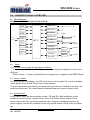
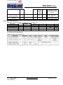
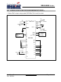
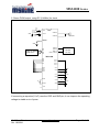
MS34100 Series M-Square Technologies Corp. A Subsidiary of Realtek G roup 8-BIT MCU BASED GENERIC INTEGRATED SYSTEM (SPEECH/MELODY/ADC/64-dots LCD/RTC/IR/WATCHDOG/ALARM CONTROLLER) General Description The MS34100 series are 8-bit MCU based generic integrated system designed for 3H(High Quality, High performance, High Reliability) speech / melody, Analog To Digital Converter (ADC), Liquid Crystal Display(LCD), Real Time Clock(RTC), Infra-Red(IR), Watch Dog and Alarm products such as intelligent educational and interactive toys. The dual channels speech and dual channels melody can be playing out simultaneously through either DAC or PWM output. These chips not only provide high quality speech / melody, but also we offer programming / coding tools for ease and flexibility in designing customers' products. MS34100 provides 8CH*8bit ADC for customers to easily receive external analog signals, such as temperature, humidity, brightness, voltage, sound…etc. MS34100 could also be used in detecting thermograph, low battery detection…etc. MS34100 provides 32 or 64 dots LCD controller (4*16 or 4*8 multi I/O) and also serves as an automatic display control er for LCD. It is very suitable for little size LCD products. RTC provides the most accurate timer’s function and low speed oscillation to conserve power consumption. The additional alarm function perfects the clock application. IR provides a pair of transmission and receiving system that ensures high performance transmission distance and accurate IR signal receiving when developing remote control system. Micro-controller Core Features Operating voltage range : 2.4V to 5.0V 304 bytes general-purpose RAM @ 2~4M Hz; 3.6V to 5.0V@6, 8M Hz 128 bytes Stack Fourteen interrupt sources in four priority levels Interrupt control Timer interrupt Input port transition Power management modes support for power saving issues Programmable CPU clock(Fcpu). Halt mode (MPU = off & timer=on) Stop mode (MPU = RTC = off ) Built-in oscillation circuit (PLL) or RC oscillation (by mask option, RC oscillator is optional, up to 4MHz) ROM: 512K internal mask ROM for MS34116 384K internal mask ROM for MS34112 A single ROM contains al progr- am and data(include speech and melody) RAM : 432 bytes V1.2 Data Sheet Oct.18/2004 . www.mshinetek.com Page 1 of 15 MS34100 Series M-Square Technologies Corp. A Subsidiary of Realtek G roup Peripheral Features 32 I/O ports : 8 Input ports a. Multiplexed with analog input of ADC. b. Built-in Schmitt trigger circuit for each PI pad. 8 General purpose output ports (PO) with high output current. 8 General purpose input/output ports (PA) with wake up function & high sink output current 8 General purpose input/output ports (PB) with wake up function. In input mode, built-in Schmitt trigger circuit for each PB pad. LCD driver are programmable to be I/O ports(PA,PB) : 4*16 Common driver ports : PO4-7(4 ports) Segment driver ports : PA,PB(16 ports) Ten 8-bit timers Two speech timers, one melody timer, two general-purpose timers that can be cascaded as one 16-bit timer, one dedicated IR timer &counter (for 38KHz or 57 KHz carrier), one watch-dog-timer V1.2 Data Sheet Oct.18/2004 LCD driver LCD power & type: VDD, Type A Bias & Duty mode: 1/3 bias, 1/4 duty Common & Segment driver pads: 4 X 16(Max.) Realtek Advanced PWM/DAC audio output Support both PWM & DAC output for different application (software programmable) and speech sampling rate can be programmed to generate speech melody Dual tone & two speech channels can be played out simultaneously Software programmable(4bit) volume combination (modes) Software programmable (4 bits) volume control could fit for variant impedance speaker. Provide 4-bit ADPCM type A and 8-bit direct PCM software algorithms for different sound quality requirements Speech length can be up to 160 (max) seconds based on 6K Hz sampling rate of 4-bit ADPCM www.mshinetek.com Page 2 of 15 MS34100 Series M-Square Technologies Corp. A Subsidiary of Realtek G roup Special Micro-controller Features ADC Built-in low-voltage-reset (LVR, typical 8 bit resolution 8 multiplexed channels input Programmable conversion rate: 2KHz ~ 16KHz Programmable reference voltage reset voltage is 2 or 3V by pin option) Built-in watchdog timer 1Hz (multifunction with random number generator) IR transmission interface source: built-in Vref (2.0V) or external input voltage Total Unadjusted Error : +/- 2.5 A programmable 6-bit counter to generate 38KHz or 57KHz carrier for infrared application. LSB Application Field Intelligent educational toy Interactive toy Home electric appliance control er Hand held LCD products Clock timers Thermometers, hygrometers, capacitor scaler V1.2 Data Sheet Oct.18/2004 www.mshinetek.com Page 3 of 15 MS34100 Series M-Square Technologies Corp. A Subsidiary of Realtek G roup 1.0 BONDING INFORMATION 1.1 Bonding Diagram and Pad Location ( If you want get this information, please contact MST sales representative. ) 1.2 Pin Out Description Pin I/O VDD Power GND Power AVDD Power AGND Power PVDD Power PGND Power OSCI I OSCO O XTLI I XTLO O PI[7..0] I PA[7..0] I/O Description Positive power supply for digital circuit Negative power supply for digital circuit Positive power supply for analog circuit Negative power supply for analog circuit Positive power supply for PWM Negative power supply for PWM. PLL oscillation input pin. PLL oscillation output pin. Input pin for 32.768KHz crystal oscillator (or RC input pin) Output pin for 32.768KHz crystal oscillator(or RC output pin) General purpose input / analog input pins with software program able pul -high resistors. Either input or analog input function is set by program. Furthermore, built-in Schmitt trigger circuit for each PI pad. General purpose input/output pins with software programable pull-high resistors. Either input or output function is set by PB[7..0] I/O PO[7..0] AU[1..0] VLCD0-3 TEST I O I I RESETB I AVREF LVR_SEL I/O I EVENB EVROMCSB D[0..7] A[0..18] I O I/O O V1.2 Data Sheet Oct. 18/2004 . program. General purpose input/output input pins with software programable pull-high resistors. Either input or output function is set by program. In input mode, built-in Schmitt trigger circuit for each PB pad General purpose output pins The audio output LCD bias resistor adjust pads Reserved for testing purpose. Pul -low resistors are built-in this pad. Reset input pin. A logical 0 on it forces the system to a known start-up state. A Schmitt trigger circuit and pul -high resistor are built-in. An external capacitor (0.47 ∝F) should be connect ed between this pad and GND. External or built-in reference voltage for ADC. LVR limitation voltage selection pin(by pin option) 0=The reset voltage is 2V(operating voltage range=2.4~ 3.3V) 1=The reset voltage is 3V.(operating voltage range=3.3~ 4.8V) EV mode enable pin External ROM (EV ROM) chip select pin Data bus for EV ROM Address bus for EV ROM www.mshinetek.com Page 4 of 15 MS34100 Series M-Square Technologies Corp. A Subsidiary of Realtek G roup WRB RDB BDM_SCLK BDM_SDI BDM_SDO BDM_EMU DVP SRAM write enable DVP/EV SRAM/ROM read enable Clock output for BDM ICE Serial data input for BDM ICE Serial data output for BDM ICE CPU operating mode select pin 0 = CPU is running under normal mode 1 = CPU is halt and enter BDM mode BDM_RSTB I On chip circuit reset pin from BDM ICE OSC_SEL I RC/PLL selection pin(mask option for main chip, EV/DVP by pin option) 0 = PLL version 1 = RC version Total: 51 Pads for MS34100 & 95 pads for MS34x00 EV/DVP V1.2 Data Sheet Oct. 18/2004 O O O I O O www.mshinetek.com Page 5 of 15 MS34100 Series M-Square Technologies Corp. A Subsidiary of Realtek G roup 2.0 ARCHITECTURAL OVERVIEW 2.1 Block Diagram FIGURE 2-1: FUNCTION BLOCK DIAGRAM Input Port Stack RAM A/D Converter ROM IR Interface Timing Control Circuit OSCI OSCO Low voltage reset Watch Dog Timer Real Time Clock PO0 Output Port PO COM1-4(PO4-7) MCU LCD Driver I/O Ports Melody1 Speech1 SEG1-16(PA0-7, PB0-7) PA,PB DAC1 AUDIO1 PWM Melody2 Speech2 2.2 PI DAC2 AUDIO2 Reset 2.4.1 A reset occurs under the fol owing conditions : * Power-on reset (POR) -- A POR is generated when a positive transition occurs on the VDD pad. * External reset -- A reset is generated when a logical zero is applied to the RESETB pad. 2.3 Power Control For saving power consumption, the CPU clock source can be gated off, even the oscillator circuit System Clock & Real Time Clock can be stopped. To reduce the power consumption, two power-saving modes are included in this chip: Halt mode and Stop mode. The main difference between these two mode is system clock. 2.4 System Clock In this system, there are two oscillation circuits : RC and PLL. Both oscillation circuits provide two clock sources : System Clock (Fosc) & 32768Hz Crystal. System Clock source comes from PLL circuit & programmer can change the oscillating frequency by control register, and the RC oscillation circuit only provide System Clock (Fosc) to system use. V1.2 Data Sheet Oct. 18/2004 www.mshinetek.com Page 6 of 15 MS34100 Series M-Square Technologies Corp. A Subsidiary of Realtek G roup 2.5 Program ROM The MS34100 normal program ROM size is 61.5k bytes. If it doesn't need so much program ROM, the remainder can be used as speech ROM. For example, if only 5.5K bytes program ROM are used, the remaining 56K bytes can store about 18 seconds of speech data. 2.6 I/O Registers and General Purpose RAM Total of 512 bytes includes 80 bytes memory-mapped I/O, 304 bytes working RAM, and 128 bytes Stack 2.7 I/O PORT The chip has 4 I/O ports : One input-only port, two I/O ports, and one output-only port. * Input-only port : PI port PI pads are general purpose input port with internal pull-high resistors (100, 200, 300 or 400K Ohm by mask option, when PI Port always connect to GND the value of pull-high resistor will be change to 1.5M, 2.5M, 2.5M or 4.5M Ohm by mask option) that can be individualy enabled by software. Each pad can be individual y enabled to generate a interrupt signal when a high-to-low or low-to-high transition occurs. * Bi-direction port : PA , PB Ports The PA, PB ports are general purpose bi-directional I/O pads with LCD segment pins and the internal pull-high resistors (150K Ohm) that can be individual y enabled by software. The contents of the data direction registers (PADR, PBDR) deter- mine each bi-directional I/O pad to be an input or an output. A logic zero means input mode and a logic one means output mode. * Output-only port : PO port PO ports are general purpose output port with LCD common pins(PO7-4). PO7 – PO0 have higher driving capability. 2.8 Analog to Digital Converter MS34100 performs an 8-bit AD conversion via successive approximation. This ADC is connected to PI ports which al ow each pad to be an analog input for this ADC. There is a sample-and-hold amplifier in the ADC to ensure that the input voltage to the ADC is held at a constant level during conversion process. Note: 1. It consumes about 2 mA while ADC operates @ 3.3V (without the loading on Vout). 2. The built-in pul -up resistance should be disabled (PIR=0) while the corresponding PI pad is set as analog input. V1.2 Data Sheet Oct. 18/2004 www.mshinetek.com Page 7 of 15 MS34100 Series M-Square Technologies Corp. A Subsidiary of Realtek G roup 3. The input voltage range is between GND and Vref 4. This ADC module performs + / -2.5 LSB accuracy. 5. The input impedance must be least than 20KΩ. 6. The rage of Vref is from 2.0V to VDD. 7. The temperature range is from –10℃ to 45℃. 8. The conversion rate = ( Fadc / [ADCPR]), where Fadc is 16K Hz. 2.9 Timers There are ten timers: General-purpose timer (GTL>H), two Speech Timers (ST1&ST2 ), Melody Timer(MT), Clock Timer(CT), Real Time Clock timer(RTCT), WatchDog Timer / Random Number Generator(WDT), Infra-Red Timer(IR-RT&IR-TT). General purpose timer is for general purpose usage, e.g., keyboard de-bounce, silence control during speech connection, elapse time counting, ..., etc. GTL and GTH can be cascaded as a 16-bit counter. Usual y, Speech timers are for controlling speech sampling rates; Melody timer is for melody rhythm; Clock and RTC timer are for real time clock, Wathdog timer are for avoiding system entering abnormal operating and also could be the a random number, generator IR Receiver timer provides an exact count for receive IR signal. Although speech, melody, Clock, and Infra-Red receiver timers are dedicated for speech sampling rate and melody rhythm control, they can also be used as general purpose timers too. In fact, these timers do not have any relation to speech, melody, Clock or IR Receiver generating hardware. 2.10 Interrupt There are fourteen interrupt sources with four priority levels. The priority order : Level1> Level2> Level3>Level4. An enabled interrupt with Level1 priority can interrupt a Level2 priority interrupt. For interrupts of the same priority can not interrupt each other. Level1 is the highest order and level4 is the lowest order. 2.11 Speech and Melody There are 2 programmable audio output: one is DAC output and another is PWM output. DAC output produces high sound quality, but consumes more power. In the other hand, PWM output consumes less power, but produces lower sound quality. Both of DAC and PWM output, there are 2 speech channels and dual tone melody which can be simultaneously played out. AUDIO1 is the combined output of speech 1 and melody 1; AUDIO2 is the combined output of speech 2 and melody 2. MS34100 PWM output provide also software programmable 16 modes output volume control (PVOL3-0) and output ratio control (PMOD3-0) feature for imporving output sound quality. V1.2 Data Sheet Oct. 18/2004 www.mshinetek.com Page 8 of 15 MS34100 Series M-Square Technologies Corp. A Subsidiary of Realtek G roup 2.12 LCD Driver interface The characteristics of LCD driver circuit are: Common driver pads: 4(PO4~7) Segment driver pads: 16(PA0~7, PB0~7) COM and SEG are multi-function I/O pads Duty mode: 1/4 duty Bias mode: 1/3 bias Frame scheme: Type A Frame Frequency (FF) : 32.6/34.1Hz (By different clock source 31250 or 32768Hz) V1.2 Data Sheet Oct. 18/2004 www.mshinetek.com Page 9 of 15 MS34100 Series M-Square Technologies Corp. A Subsidiary of Realtek G roup 3.0 ELECTRICAL CHARACTERISTICS DC Electrical Characteristics (Fosc=2MHz, TA=25°C) Pad Min. Typ. Max. Operating Voltage Symb ol VDD VDD 2.4V -- 5.0V Low Voltage Reset VLVR VDD 2.0V -- 3.0V Tolerance=+/-0.2V PI, PB -- 3/5VDD -- Schmitt Trigger Circuit -- 1/2VDD -- CMOS LEVEL -- 2/5VDD -- Schmitt Trigger Circuit -- 1/2VDD -- CMOS LEVEL - - Parameter Vih Input High Voltage PA,TEST2-1, RESETB PI, PB Input Low Voltage Output High Voltage Output Low Voltage Condition Vil PA, TEST2-1 Voh1 RESETB PA, PB , PO3-0 Voh2 PO7-4 0.8VDD - - Ioh1 = -1.0mA Ioh2 = -2.0mA Vol1 PA, PB , PO3-0 - - 0.2VDD Iol1 = 1.6mA Vol2 PO7-4 - - 0.2VDD Iol2 = 10mA Iop VDD -- 2mA -- No load, VDD=3V, RC -- 1.5mA -- No load, VDD=3V, PLL - 0.5mA -- No load, VDD=3V, PLL Operating Current 0.8VDD CPU-Halt1 Mode Current Ihalt1 VDD CPU-Halt2 Mode Current Ihalt2 VDD - 10uA -- Istop VDD - - 1uA Hz, PLL&RC No load IDAC AUDIO1,2 1.0mA 3.0mA -- Voh = 0.7V IPWM AUDIO1,2 -- 110mA -- Loading = 10Ohm PO0-7 -- 22mA -- PA, PB -- 15mA -- PO0-7, PA -- 9mA -- Stop Mode Current AUDIO DAC Output Current AUDIO PWM Output Current 0.2mA No load, VDD=3V, PLL LCD=on&Fcpu=32768 Voh = 2.4V, VDD=4.5V Output Driving Current Idriving Vol = 0.4V, VDD=4.5V Output Sinking Current PB -- 5.0mA -- PO0-7, PA -- 22mA -- PB -- 13mA -- PA, PB, PI, TEST -- 150KΩ -- -- 100KΩ 200KΩ 300KΩ 400KΩ Vol = 1.0V, VDD=4.5V Isinking RESETB Input Pull high resistance V1.2 Data Sheet Oct. 18/2004 VDD=3V Rin PI When input pin is connected to GND, www.mshinetek.com When PI pin is -- connected to 2/3VDD VDD=2.4V Page 10 of 15 MS34100 Series M-Square Technologies Corp. A Subsidiary of Realtek G roup -Oscil ator Frequency Variation (process) Oscil ator Frequency Stability - △ F/F 1.5MΩ 2.5MΩ 3.5MΩ 4.5MΩ -- 5% -- -- When PI pin is connected to GND, VDD=3V RC, VDD=3.0V RC, △ F/F - -- 8% -- |F(3.2V)-F(2.4V)| / F(3.2V) or |F(4.8V)-F(3.6V)| / F(4.8V) 8-bit ADC Characteristics o (Resonator / Crystal Oscillator, TA=-40 to 85 C, VDD=3.6 to 5.5V) MIN. Parameter Symbol Conditions Resolution Total unadjusted error Conversion time TCONV Analog input voltage VAIN TYP. 8 ---- ----- 8 -64 0 Pad XTLI, XTLO Min. Typ. 2MHz 4MHz 8ms Unit bits LSB uS V MAX. 8 ±2.5 250 AVref AC Electrical Characteristics (VDD = 5V, VSS = 0V, TA = 25 C) Parameter Oscil ation Frequency Oscil ator Stabilization Time Enable to Data Valid Disable to Data Invalid V1.2 Data Sheet Oct. 18/2004 Symbol Fosc Tstb Tedv Tddi XTLI, XTLO -600ms D7-0 D7-0 0ns www.mshinetek.com - Max. 8MHz --- Test Condition Varied with VDD For RC For PLL 1000/Fosc-15ns - --- Page 11 of 15 MS34100 Series M-Square Technologies Corp. A Subsidiary of Realtek G roup 4.0 APPLICATION CIRCUIT(FOR REFERENCE ONLY) 1. Stereo DAC output, using crystal (32768Hz, PLL circuit) for clock VCC 22 pF XTLI AUDIO1 Y1 GND 8050 SPEAKER 1 KW 32768Hz 22 pF XTLO GND 1 KW RESET AUDIO2 8050 0.47 uF GND Analog To Digital Signal Input VCC PI0 COM1-4 (PO4-7) PI1 PI2 SEG1-16 (PA0-7, PB0-7) SPEAKER LCD Panel 1/3 bias 1/4 duty PI3 MS34100 PI4 PI5 PI6 PI7 VLCD0 VLCD 1 VLCD 2 VLCD3 PO0 PO1 PO2 PO3 Key Matrix VCC VDD 0.1uF GND PVDD VDD 0.1uF PGND 0.1uF 4.7KW OSCI GND AVDD OSCO VDD 0.1uF AGND TEST V1.2 Data Sheet Oct. 18/2004 . www.mshinetek.com Page 12 of 15 MS34100 Series M-Square Technologies Corp. A Subsidiary of Realtek G roup 2. Stereo PWM output, using RC (2-4MHz) for clock 22 pF XTLI Y1 32768Hz GND 22 pF XTLO AUDIO1 AUDIO2 SPEAKER RESET 0.47 uF GND Analog To Digital Signal Input PI0 COM1-4 (PO4-7) PI1 PI2 SEG1-16 (PA0-7, PB0-7) LCD Panel 1/3 bias 1/4 duty PI3 MS34100 PI4 PI5 PI6 PI7 VLCD 0 VLCD 1 VLCD 2 VLCD 3 PO0 PO1 PO2 PO3 VDD 0.1uF GND Key Matrix PVDD VDD 0.1uF PGND OSCI AVDD R VDD 0.1uF OSCO AGND TEST If connecting a capacitor(0.1uF) near the VDD and GND pin, it can improve the operating voltage to stable on the System. V1.2 Data Sheet Oct. 18/2004 www.mshinetek.com Page 13 of 15 MS34100 Series M-Square Technologies Corp. A Subsidiary of Realtek G roup 5.0 DEVELOPMENT TOOLS M-SQUARE Technologies Corp. provides MS34x00 EV/DVP board for programming evaluation and for source level debugging. These tools helps the users develop and verify the application conveniently. Please reference user’s manual of RT-SLD and MS34x00 DVP user’s guide for more information. FINGURE 11-1 : MS34100 EV/DVP BOARD BLOCK DIAGRAM Host PC SRAM(256K or 512K byte) or EPROM(128K ~ 512K byte) RS232 SRAM EPROM MS34x00 DVP Chip With build-in BDM circuit BDM Interface RT-ICE Board Cable of LCD driver pads Cable of I/O & AUDIO pads (to target board) V1.2 Data Sheet Oct. 18/2004 e www.mshinetek.com Page 14 of 14