1
PicoBlaze Interface Signals
1
PicoBlaze Interface Signals
Introduction
PicoBlaze
PicoBlaze Functional Blocks
2
PicoBlaze Interface Signals
3
Instruction Set
4
Interrupts
5
Scratchpad RAM
6
Input and Output Ports
Input Operations
Output Operations
PicoBlaze Interface
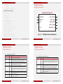
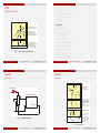
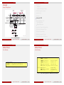
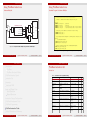
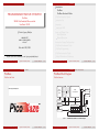
PicoBlaze Interface Connections
PicoBlaze Microcontroller
IN_PORT[7:0]
INTERRUPT
PORT_ID[7:0]
RESET
READ_STROBE
WRITE_STROBE
7
Instruction Storage Configurations
8
PicoBlaze Development Tools
9
PicoBlaze Programming
10
PicoBlaze Instruction Codes
11
Related Materials and References
J
c Dr inż. Ignacy Pardyka (Inf ∈ UK
)
OUT_PORT[7:0]
INTERRUPT_ACK
CLK
UG129_c2_01_052004
Figure 2-1:
programowanie struktur cyfrowych
Rok akad. 2011/2012
5 / 96
J
c Dr inż. Ignacy Pardyka (Inf ∈ UK
)
PicoBlaze Interface Signals
PicoBlaze Interface Connections
programowanie struktur cyfrowych
6 / 96
PicoBlaze Interface Signals
PicoBlaze Interface
PicoBlaze Interface
PicoBlaze Interface Signals
PicoBlaze Interface Signals cont’d
Table 2-1:
Rok akad. 2011/2012
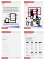
PicoBlaze Interface Signal Descriptions
Signal
IN_PORT[7:0]
Direction
Description
Input
Input Data Port: Present valid input data on this port during an INPUT instruction.
The data is captured on the rising edge of CLK.
INTERRUPT
Input
Interrupt Input: If the INTERRUPT_ENABLE flag is set by the application code,
generate an INTERRUPT Event by asserting this input High for at least two CLK
cycles. If the INTERRUPT_ENABLE flag is cleared, this input is ignored.
RESET
Input
Reset Input: To reset the PicoBlaze microcontroller and to generate a RESET Event,
assert this input High for at least one CLK cycle. A Reset Event is automatically
generated immediately following FPGA configuration.
CLK
Input
Clock Input: The frequency may range from DC to the maximum operating
frequency reported by the Xilinx ISE® development software. All PicoBlaze
synchronous elements are clocked from the rising clock edge. There are no clock
duty-cycle requirements beyond the minimum pulse width requirements of the
FPGA.
OUT_PORT[7:0]
Output
Output Data Port: Output data appears on this port for two CLK cycles during an
OUTPUT instruction. Capture output data within the FPGA at the rising CLK edge
when WRITE_STROBE is High.
PORT_ID[7:0]
Output
Port Address: The I/O port address appears on this port for two CLK cycles during
an INPUT or OUTPUT instruction.
J
c Dr inż. Ignacy Pardyka (Inf ∈ UK
)
programowanie struktur cyfrowych
Rok akad. 2011/2012
Table 2-1:
PicoBlaze Interface Signal Descriptions (Cont’d)
Signal
7 / 96
Direction
Description
READ_STROBE
Output
Read Strobe: When asserted High, this signal indicates that input data on the
IN_PORT[7:0] port was captured to the specified data register during an INPUT
instruction. This signal is asserted on the second CLK cycle of the two-cycle INPUT
instruction. This signal is typically used to acknowledge read operations from
FIFOs.
WRITE_STROBE
Output
Write Strobe: When asserted High, this signal validates the output data on the
OUT_PORT[7:0] port during an OUTPUT instruction. This signal is asserted on the
second CLK cycle of the two-cycle OUTPUT instruction. Capture output data
within the FPGA on the rising CLK edge when WRITE_STROBE is High.
INTERRUPT_ACK
Output
Interrupt Acknowledge: When asserted High, this signal acknowledges that an
INTERRUPT Event occurred. This signal is asserted during the second CLK cycle
of the two-cycle INTERRUPT Event. This signal is optionally used to clear the
source of the INTERRUPT input.
J
c Dr inż. Ignacy Pardyka (Inf ∈ UK
)
programowanie struktur cyfrowych
Rok akad. 2011/2012
8 / 96