1
USER GUIDE
Atmel XMEGA A1U Xplained Pro
Preface
®
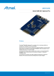
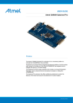
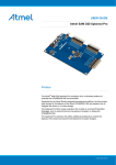
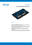
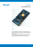
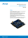
The Atmel XMEGA A1U Xplained Pro evaluation kit is a hardware platform to
evaluate the ATxmega128A1U microcontroller.
Supported by the Atmel Studio integrated development platform, the kit provides
easy access to the features of the Atmel ATxmega128A1U and explains how to
integrate the device in a custom design.
The Xplained Pro MCU series evaluation kits include an on-board Embedded
Debugger, and no external tools are necessary to program or debug the
ATxmega128A1U.
The Xplained Pro extension kits offers additional peripherals to extend the
features of the board and ease the development of custom designs.
42211A-MCU-01/2014
Table of Contents
Preface .......................................................................................... 1
1. Introduction .............................................................................. 3
1.1.
1.2.
Features .............................................................................. 3
Kit overview ......................................................................... 3
2. Getting started ......................................................................... 5
2.1.
2.2.
2.3.
Quick-start ........................................................................... 5
Connecting the kit ................................................................. 5
Design documentation and related links ..................................... 5
3. Xplained Pro ............................................................................ 6
3.1.
3.2.
3.3.
3.4.
Embedded Debugger ............................................................. 6
Hardware identification system ................................................. 6
Power supply ....................................................................... 7
3.3.1.
Measuring XMEGA power consumption ......................... 7
Standard headers and connectors ............................................ 7
3.4.1.
Xplained Pro standard extension header ........................ 7
3.4.2.
Xplained Pro LCD connector ....................................... 8
3.4.3.
Xplained Pro power header ....................................... 10
4. Hardware user guide ............................................................ 11
4.1.
4.2.
4.3.
4.4.
4.5.
Connectors .........................................................................
4.1.1.
I/O extension headers ..............................................
LCD extension connector ......................................................
Other headers .....................................................................
Peripherals .........................................................................
4.4.1.
Crystal ...................................................................
4.4.2.
Mechanical buttons ..................................................
4.4.3.
LED ......................................................................
4.4.4.
USB ......................................................................
4.4.5.
SRAM ...................................................................
Embedded Debugger implementation ......................................
4.5.1.
Program Debug Interface ..........................................
4.5.2.
Virtual COM port .....................................................
4.5.3.
Atmel Data Gateway Interface ...................................
11
11
12
14
14
14
15
15
15
15
16
16
16
16
5. Hardware revision history and known issues ........................ 18
5.1.
5.2.
Identifying product ID and revision .......................................... 18
Revision 2 .......................................................................... 18
6. Document revision history ..................................................... 19
7. Evaluation board/kit important notice .................................... 20
Atmel XMEGA A1U Xplained Pro [USER GUIDE]
42211A-MCU-01/2014
2
1.
Introduction
1.1
Features
●
Atmel ATxmega128A1U microcontroller
●
Embedded debugger (EDBG)
●
●
1.2
●
USB interface
●
Programming and debugging on board XMEGA through PDI
●
Virtual COM-port interface to target via UART
●
Atmel Data Gateway Interface (DGI) to target via USART and TWI
●
Four GPIOs connected to target for code instrumentation
®
Digital I/O
●
Two mechanical buttons (user and reset button)
●
One user LED
●
Three extension headers
●
Xplained Pro LCD extension connector
Three possible power sources
●
External power
●
Embedded debugger USB
●
Target USB
●
32kHz crystal
●
External 512KB SRAM
●
USB interface, device mode
Kit overview
The Atmel XMEGA A1U Xplained Pro evaluation kit is a hardware platform to evaluate the Atmel
ATxmega128A1U.
The kit offers a set of features that enables the ATxmega128A1U user to get started using the XMEGA
peripherals right away and to get an understanding of how to integrate the device in their own design.
Atmel XMEGA A1U Xplained Pro [USER GUIDE]
42211A-MCU-01/2014
3
Figure 1-1. XMEGA A1U Xplained Pro evaluation kit overview
Atmel XMEGA A1U Xplained Pro [USER GUIDE]
42211A-MCU-01/2014
4
2.
Getting started
2.1
Quick-start
3 Steps to start exploring the Atmel Xplained Pro Platform
2.2
1
●
Download and install Atmel Studio
●
Launch Atmel Studio
●
Connect a USB micro B cable to the DEBUG USB port
Connecting the kit
When connecting Atmel XMEGA A1U Xplained Pro to your computer for the first time, the operating system will
®
®
do a driver software installation. The driver file supports both 32-bit and 64-bit versions of Microsoft Windows
XP and Windows 7.
Once connected the green power LED will be lit and Atmel Studio will autodetect which Xplained Pro
evaluation- and extension kit(s) that's connected. You'll be presented with relevant information like datasheets
and kit documentation. You also have the option to launch Atmel Software Framework (ASF) example
applications. The target device is programmed and debugged by the on-board Embedded Debugger and no
2
external programmer or debugger tool is needed. Please refer to the Atmel Studio user guide for information
regarding how to compile and program the kit.
2.3
Design documentation and related links
The following list contains links to the most relevant documents and software for XMEGA A1U Xplained Pro.
3
1.
Xplained Pro products - Atmel Xplained Pro is a series of small-sized and easy-to-use evaluation kits
for 8- and 32-bit Atmel microcontrollers. It consists of a series of low cost MCU boards for evaluation and
demonstration of features and capabilities of different MCU families.
2.
XMEGA A1U Xplained Pro User Guide - PDF version of this User Guide.
3.
XMEGA A1U Xplained Pro Design Documentation - Package containing schematics, BOM, assembly
drawings, 3D plots, layer plots etc.
4.
EDBG User Guide - User guide containing more information about the onboard Embedded Debugger.
5.
Atmel Studio - Free Atmel IDE for development of C/C++ and assembler code for Atmel
microcontrollers.
6.
IAR Embedded Workbench
for Atmel AVR . This is a commercial C/C++ compiler that is available for
8-bit AVR. There is a 30 day evaluation version as well as a 4k code size limited kick-start version available
from their website.
7.
Atmel sample store - Atmel sample store where you can order samples of devices.
4
5
6
7
®8
®
9
1
http://www.atmel.com/atmelstudio
http://www.atmel.com/atmelstudio
3
http://www.atmel.com/XplainedPro
4
http://www.atmel.com/Images/Atmel-42211-XMEGA-A1U-Xplained-Pro_User-Guide.pdf
5
http://www.atmel.com/Images/Atmel-42211-XMEGA-A1U-Xplained-Pro_User-Guide.zip
6
http://www.atmel.com/Images/Atmel-42096-Microcontrollers-Embedded-Debugger_User-Guide.pdf
7
http://www.atmel.com/atmelstudio
8
http://www.iar.com/en/Products/IAR-Embedded-Workbench/AVR/
9
http://www.atmel.com/system/samplesstore
2
Atmel XMEGA A1U Xplained Pro [USER GUIDE]
42211A-MCU-01/2014
5
3.
Xplained Pro
Xplained Pro is an evaluation platform that provides the full Atmel microcontroller experience. The platform
consists of a series of Microcontroller (MCU) boards and extension boards that are integrated with Atmel
Studio, have Atmel Software Framework (ASF) drivers and demo code, support data streaming and more.
Xplained Pro MCU boards support a wide range of Xplained Pro extension boards that are connected through
a set of standardized headers and connectors. Each extension board has an identification (ID) chip to uniquely
identify which boards are mounted on a Xplained Pro MCU board. This information is used to present relevant
user guides, application notes, datasheets and example code through Atmel Studio. Available Xplained Pro
1
MCU and extension boards can be purchased in the Atmel Web Store .
3.1
Embedded Debugger
The XMEGA A1U Xplained Pro contains the Atmel Embedded Debugger (EDBG) for on-board debugging. The
EDBG is a composite USB device of 3 interfaces; a debugger, Virtual COM Port and Data Gateway Interface
(DGI).
In conjunction with Atmel Studio, the EDBG debugger interface can program and debug the ATxmega128A1U.
On the XMEGA A1U Xplained Pro, the PDI interface is connected between the EDBG and the
ATxmega128A1U.
The Virtual COM Port is connected to a UART port on the ATxmega128A1U (see section “Embedded
Debugger implementation” on page 16 for pinout), and provides an easy way to communicate with the target
application through simple terminal software. It offers variable baud rate, parity and stop bit settings. Note that
the settings on the target device UART must match the settings given in the terminal software.
The DGI consists of several physical data interfaces for communication with the host computer. Please,
see section “Embedded Debugger implementation” on page 16 for available interfaces and pinout.
Communication over the interfaces are bidirectional. It can be used to send events and values from the
ATxmega128A1U, or as a generic printf-style data channel. Traffic over the interfaces can be timestamped
on the EDBG for more accurate tracing of events. Note that timestamping imposes an overhead that reduces
maximal throughput. The DGI uses a proprietary protocol, and is thus only compatible with Atmel Studio.
The EDBG controls two LEDs on XMEGA A1U Xplained Pro, a power LED and a status LED. Table 3-1,
“EDBG LED control” on page 6 shows how the LEDs are controlled in different operation modes.
Table 3-1. EDBG LED control
Operation mode
Power LED
Status LED
Normal operation
Power LED is lit when power is
applied to the board.
Activity indicator, LED flashes
every time something happens on
the EDBG.
Bootloader mode (idle)
The power LED and the status LED blinks simultaneously.
Bootloader mode (firmware
upgrade)
The power LED and the status LED blinks in an alternating pattern.
2
For further documentation on the EDBG, see the EDBG User Guide .
3.2
Hardware identification system
All Xplained Pro compatible extension boards have an Atmel ATSHA204 CryptoAuthentication™ chip mounted.
This chip contains information that identifies the extension with its name and some extra data. When an
Xplained Pro extension board is connected to an Xplained Pro MCU board the information is read and sent
to Atmel Studio. The Atmel Kits extension, installed with Atmel Studio, will give relevant information, code
examples and links to relevant documents. Table 3-2, “Xplained Pro ID Chip Content” on page 6 shows the
data fields stored in the ID chip with example content.
Table 3-2. Xplained Pro ID Chip Content
1
2
Data Field
Data Type
Example Content
Manufacturer
ASCII string
Atmel’\0’
Product Name
ASCII string
Segment LCD1 Xplained Pro’\0’
Product Revision
ASCII string
02’\0’
Product Serial Number
ASCII string
1774020200000010’\0’
http://store.atmel.com/CBC.aspx?q=c:100113
http://www.atmel.com/Images/Atmel-42096-Microcontrollers-Embedded-Debugger_User-Guide.pdf
Atmel XMEGA A1U Xplained Pro [USER GUIDE]
42211A-MCU-01/2014
6
3.3
Data Field
Data Type
Example Content
Minimum Voltage [mV]
uint16_t
3000
Maximum Voltage [mV]
uint16_t
3600
Maximum Current [mA]
uint16_t
30
Power supply
The XMEGA A1U Xplained Pro kit can be powered either by USB or by an external power source through the
4-pin power header, marked PWR. This connector is described in “Xplained Pro power header” on page 10.
The available power sources and specifications are listed in Table 3-3, “Power sources for XMEGA A1U
Xplained Pro” on page 7.
Table 3-3. Power sources for XMEGA A1U Xplained Pro
Power input
Voltage requirements
Current requirements
Connector marking
External power
5V +/- 2 % (+/- 100mV)
for USB host operation.
Recommended
minimum is 1A to
be able to provide
enough current for
connected USB
devices and the board
itself. Recommended
maximum is 2A due
to the input protection
maximum current
specification.
PWR
4.3 V to 5.5 V if USB
host operation is not
required
Embedded debugger
USB
4.4V to 5.25V
(according to USB spec)
500 mA (according to
USB spec)
DEBUG USB
Target USB
4.4V to 5.25V
(according to USB spec)
500 mA (according to
USB spec)
TARGET USB
The kit will automatically detect which power sources are available and choose which one to use according to
the following priority:
Note
3.3.1
1.
External power
2.
Embedded debugger USB
3.
Target USB
External power is required when the 500mA through the USB connector is not enough to power a
connected USB device in a USB host application.
Measuring XMEGA power consumption
As part of an evaluation of the XMEGA it can be of interest to measure its power consumption. Because the
device has a separate power plane (VCC_MCU_P3V3) on this board it is possible to measure the current
consumption by measuring the current that is flowing into this plane. The VCC_MCU_P3V3 plane is connected
via a jumper to the main power plane (VCC_TARGET_P3V3) and by replacing the jumper with an ampere
meter it is possible to determine the current consumption. To locate the current measurement header, please
refer to Figure 1-1, “XMEGA A1U Xplained Pro evaluation kit overview” on page 4.
Warning
Do not power the board without having the jumper or an ampere meter mounted. This can cause
the XMEGA to be powered through its I/O pins and cause undefined operation of the device.
3.4
Standard headers and connectors
3.4.1
Xplained Pro standard extension header
All Xplained Pro kits have one or more dual row, 20-pin, 100mil extension headers. Xplained Pro MCU boards
have male headers while Xplained Pro extensions have their female counterparts. Note that all pins are
not always connected. However, all the connected pins follow the defined pin-out described in Table 3-4,
Atmel XMEGA A1U Xplained Pro [USER GUIDE]
42211A-MCU-01/2014
7
“Xplained Pro extension header” on page 8. The extension headers can be used to connect a wide variety
of Xplained Pro extensions to Xplained Pro MCU boards and to access the pins of the target MCU on Xplained
Pro MCU board directly.
Table 3-4. Xplained Pro extension header
3.4.2
Pin number
Name
Description
1
ID
Communication line to the ID chip on extension board.
2
GND
Ground.
3
ADC(+)
Analog to digital converter , alternatively positive part of
differential ADC.
4
ADC(-)
Analog to digital converter , alternatively negative part of
differential ADC.
5
GPIO1
General purpose I/O.
6
GPIO2
General purpose I/O.
7
PWM(+)
Pulse width modulation , alternatively positive part of
differential PWM.
8
PWM(-)
Pulse width modulation , alternatively positive part of
differential PWM.
9
IRQ/GPIO
Interrupt request line and/or general purpose I/O.
10
SPI_SS_B/GPIO
Slave select for SPI and/or general purpose I/O.
11
TWI_SDA
Data line for two-wire interface. Always implemented, bus
type.
12
TWI_SCL
Clock line for two-wire interface. Always implemented, bus
type.
13
USART_RX
Receiver line of Universal Synchronous and Asynchronous
serial Receiver and Transmitter.
14
USART_TX
Transmitter line of Universal Synchronous and
Asynchronous serial Receiver and Transmitter.
15
SPI_SS_A
Slave select for SPI. Should be unique if possible.
16
SPI_MOSI
Master out slave in line of Serial peripheral interface. Always
implemented, bus type.
17
SPI_MISO
Master in slave out line of Serial peripheral interface. Always
implemented, bus type.
18
SPI_SCK
Clock for Serial peripheral interface. Always implemented,
bus type.
19
GND
Ground.
20
VCC
Power for extension board.
Xplained Pro LCD connector
The LCD connector provides the ability to connect to display extensions that have a parallel interface. The
connector implements signals for a MCU parallel bus interface and a LCD controller interface as well as
signals for a touchcontroller. The connector pin-out definition is shown in Table 3-5, “Xplained Pro LCD
connector” on page 8. Note that usually only one display interface is implemented, either LCD controller or
the MCU bus interface.
A FPC/FFC connector with 50 pins and 0.5mm pitch is used for the LCD connector. The connector
(XF2M-5015-1A) from Omron is used on several designs and can be used as a reference.
Table 3-5. Xplained Pro LCD connector
Pin number
Name
1
ID
2
GND
3
D0
RGB interface
description
MCU interface
description
Communication line to ID chip on extension board.
Ground
Data line
Atmel XMEGA A1U Xplained Pro [USER GUIDE]
42211A-MCU-01/2014
8
Pin number
Name
RGB interface
description
MCU interface
description
4
D1
Data line
5
D2
Data line
6
D3
Data line
7
GND
8
D4
Data line
9
D5
Data line
10
D6
Data line
11
D7
Data line
12
GND
13
D8
Data line
14
D9
Data line
15
D10
Data line
16
D11
Data line
17
GND
Ground
18
D12
Data line
19
D12
Data line
20
D14
Data line
21
D15
Data line
22
GND
Ground
23
D16
Data line
24
D17
Data line
25
D18
Data line
26
D19
Data line
27
GND
Ground
28
D20
Data line
29
D21
Data line
30
D22
Data line
31
D23
Data line
32
GND
Ground
33
PCLK /
CMD_DATA_SEL
Pixel clock
and data select. One
address line of the
MCU select either the
Command register or
the data interface.
34
VSYNC / CS
Vertical synchronization
Chip select
35
HSYNC / WE
Horizontal
synchronization
Write enable signal
36
DATA ENABLE / RE
Data enable signal
Read enable signal
37
SPI SCK
Clock for Serial peripheral interface
38
SPI MOSI
Master out slave in line of Serial peripheral interface
39
SPI MISO
Master in slave out line of Serial peripheral interface
40
SPI SS
41
ENABLE
Display enable signal
42
TWI SDA
I2C data line (maxTouch )
Ground
Ground
Slave select for SPI. Should be unique if possible
®
Atmel XMEGA A1U Xplained Pro [USER GUIDE]
42211A-MCU-01/2014
9
3.4.3
Pin number
Name
RGB interface
description
MCU interface
description
43
TWI SCL
44
IRQ1
maxTouch interrupt line
45
IRQ2
Interrupt line for other I2C devices
46
PWM
Backlight control
47
RESET
48
VCC
3.3V power supply for extension board
49
VCC
3.3V power supply for extension board
50
GND
Ground
I2C clock line (maxTouch)
Reset for both display and maxTouch
Xplained Pro power header
The power header can be used to connect external power to the XMEGA A1U Xplained Pro kit. The kit will
automatically detect and switch to the external power if supplied. The power header can also be used as supply
for external peripherals or extension boards. Care must be taken not to exceed the total current limitation of the
on-board regulator for the 3.3V regulated output. To locate the current measurement header, please refer to
Figure 1-1, “XMEGA A1U Xplained Pro evaluation kit overview” on page 4
Table 3-6. Power header PWR
Note
Pin number PWR header
Pin name
Description
1
VEXT_P5V0
External 5V input
2
GND
Ground
3
VCC_P5V0
Unregulated 5V (output, derived
from one of the input sources)
4
VCC_P3V3
Regulated 3.3V (output, used as
main power for the kit)
If the board is powered from a battery source it is recommended to use the PWR header. If there
is a power source connected to EDBG USB, the EDBG is activated and it will consume more
power.
Atmel XMEGA A1U Xplained Pro [USER GUIDE]
42211A-MCU-01/2014
10
4.
Hardware user guide
4.1
Connectors
This chapter describes the implementation of the relevant connectors and headers on XMEGA A1U Xplained
Pro and their connection to the ATxmega128A1U. The tables of connections in this chapter also describes
which signals are shared between the headers and on-board functionality.
4.1.1
I/O extension headers
The XMEGA A1U Xplained Pro headers EXT1, EXT2 and EXT3 offer access to the I/O of the microcontroller
in order to expand the board e.g. by connecting extensions to the board. These headers all comply with the
standard extension header specified in Xplained Pro Standard Extension Header on page 7. All headers have a
pitch of 2.54 mm.
Table 4-1. Extension header EXT1
Pin on EXT1
XMEGA pin
Function
Shared functionality
1 [ID]
-
-
Communication line to ID chip on
extension board.
2 [GND]
-
-
GND
3 [ADC(+)]
PA0
ADCA0 (GAINPOS)
Alternate signal header
4 [ADC(-)]
PA4
ADCA4 (GAINNEG)
5 [GPIO1]
PE6
GPIO
6 [GPIO2]
PE7
GPIO
7 [PWM(+)]
PE1
TCC0 OC0B
8 [PWM(-)]
PE0
TCC0 OC0A
9 [IRQ/GPIO]
PR0
GPIO
10 [SPI_SS_B/GPIO]
PR1
GPIO
11 [TWI_SDA]
PC0
TWIC SDA
EDBG and LCD Connector
12 [TWI_SCL]
PC1
TWIC SCL
EDBG and LCD Connector
13 [USART_RX]
PC2
USARTC0 RXD0
14 [USART_TX]
PC3
USARTC0 TXD0
15 [SPI_SS_A]
PC4
SPIC SS
16 [SPI_MOSI]
PC5
SPIC MOSI
EXT2, EXT3, and LCD Connector
17 [SPI_MISO]
PC6
SPIC MISO
EXT2, EXT3, LCD Connector,
and Alternate signal header
18 [SPI_SCK]
PC7
SPIC SCK
EXT2, EXT3, LCD Connector,
and Alternate signal header
19 [GND]
-
-
GND
20 [VCC]
-
-
VCC
Alternate signal header
Table 4-2. Extension header EXT2
Pin on EXT2
XMEGA pin
Function
Shared functionality
1 [ID]
-
-
Communication line to ID chip on
extension board.
2 [GND]
-
-
GND
3 [ADC(+)]
PA1
ADCA1 (GAINPOS)
4 [ADC(-)]
PA6
ADCA6 (GAINNEG)
5 [GPIO1]
PB4
GPIO
6 [GPIO2]
PB5
GPIO
Alternate signal header
Atmel XMEGA A1U Xplained Pro [USER GUIDE]
42211A-MCU-01/2014
11
Pin on EXT2
XMEGA pin
Function
Shared functionality
7 [PWM(+)]
PE5
TCE1 OC1B
8 [PWM(-)]
PE4
TCE1 OC1A
9 [IRQ/GPIO]
PB6
GPIO
Alternate signal header
10 [SPI_SS_B/GPIO]
PB7
GPIO
Alternate signal header
11 [TWI_SDA]
PF0
TWIF SDA
EXT3
12 [TWI_SCL]
PF1
TWIF SCL
EXT3
13 [USART_RX]
PF2
USARTF0 RXD0
14 [USART_TX]
PF3
USARTF0 TXD0
15 [SPI_SS_A]
PF4
GPIO
16 [SPI_MOSI]
PC5
SPIC MOSI
EXT1, EXT3, and LCD Connector
17 [SPI_MISO]
PC6
SPIC MISO
EXT1, EXT3, LCD Connector,
and Alternate signal header
18 [SPI_SCK]
PC7
SPIC SCK
EXT1, EXT3, LCD Connector,
and Alternate signal header
19 [GND]
-
-
GND
20 [VCC]
-
-
VCC
Table 4-3. Extension header EXT3
4.2
Pin on EXT3
XMEGA pin
Function
Shared functionality
1 [ID]
-
-
Communication line to ID chip on
extension board.
2 [GND]
-
-
GND
3 [ADC(+)]
PA3
ADCA3 (GAINPOS)
4 [ADC(-)]
PA7
ADCA7 (GAINNEG)
5 [GPIO1]
PK0
GPIO
6 [GPIO2]
PK1
GPIO
7 [PWM(+)]
PD5
TCD1 OC1B
8 [PWM(-)]
PD4
TCD1 OC1A
9 [IRQ/GPIO]
PK2
GPIO
10 [SPI_SS_B/GPIO]
PK3
GPIO
11 [TWI_SDA]
PF0
TWIF SDA
EXT2
12 [TWI_SCL]
PF1
TWIF SCL
EXT2
13 [USART_RX]
PF6
USARTF1 RXD1
14 [USART_TX]
PF7
USARTF1 TXD1
15 [SPI_SS_A]
PD0
GPIO
16 [SPI_MOSI]
PC5
SPIC MOSI
EXT1, EXT2, and LCD Connector
17 [SPI_MISO]
PC6
SPIC MISO
EXT1, EXT2, LCD Connector,
and Alternate signal header
18 [SPI_SCK]
PC7
SPIC SCK
EXT1, EXT2, LCD Connector,
and Alternate signal header
19 [GND]
-
-
GND
20 [VCC]
-
-
VCC
Alternate signal header
LCD extension connector
Extension connector EXT4 is a special connector for LCD displays. The physical connector is a TE
Connectivity 5-1734839-0 FPC connector.
Atmel XMEGA A1U Xplained Pro [USER GUIDE]
42211A-MCU-01/2014
12
Table 4-4. LCD display connector EXT4
Pin on EXT4
XMEGA pin
Function
Shared functionality
1 [ID]
-
-
Communication line to ID chip on
extension board.
2 [GND]
-
-
GND
3 [D0]
PJ0
D0
SRAM
4 [D1]
PJ1
D1
SRAM
5 [D2]
PJ2
D2
SRAM
6 [D3]
PJ3
D3
SRAM
7 [GND]
-
-
GND
8 [D4]
PJ4
D4
SRAM
9 [D5]
PJ5
D5
SRAM
10 [D6]
PJ6
D6
SRAM
11 [D7]
PJ7
D7
SRAM
12 [GND]
-
-
GND
13 [D8]
-
-
14 [D9]
-
-
15 [D10]
-
-
16 [D11]
-
-
17 [GND]
-
-
18 [D12]
-
-
19 [D13]
-
-
20 [D14]
-
-
21 [D15]
-
-
22 [GND]
-
-
23 [D16]
-
-
24 [D17]
-
-
25 [D18]
-
-
26 [D19]
-
-
27 [GND]
-
-
28 [D20]
-
-
29 [D21]
-
-
30 [D22]
-
-
31 [D23]
-
-
32 [GND]
-
-
GND
33 [PCLK / CMD_DATA_SEL]
PJ0 ALE1
A0
SRAM
34 [VSYNC / CS]
PH7
EBI CS3
35 [HSYNC / WE]
PH0
EBI NWE
SRAM
36 [DATA ENABLE / RE]
PH1
EBI NRD
SRAM
37 [SPI SCK]
PC7
SPIC SCK
EXT1, EXT2, EXT3, and
Alternate signal header
38 [SPI MOSI]
PC5
SPIC MOSI
EXT1, EXT2, and EXT3
39 [SPI MISO]
PC6
SPIC MISO
EXT1, EXT2, EXT3, and
Alternate signal header
40 [SPI SS]
PB1
GPIO
GND
GND
GND
Atmel XMEGA A1U Xplained Pro [USER GUIDE]
42211A-MCU-01/2014
13
4.3
Pin on EXT4
XMEGA pin
Function
Shared functionality
41 [DISP ENABLE]
PK5
GPIO
EDBG DGI
42 [TWI SDA]
PC0
TWIC SDA
EXT1 and EDBG
43 [TWI SCL]
PC1
TWIC SCL
EXT1 and EDBG
44 [IRQ1]
PK4
GPIO
EDBG DGI
45 [IRQ2]
PK6
GPIO
EDBG DGI
46 [PWM]
PF5
TCF1 OC1B
47 [RESET]
PA5
GPIO
48 [VCC]
-
VCC_P3V3
49 [VCC]
-
VCC_P3V3
50 [GND]
-
GND
Other headers
In addition to the “I/O extension headers” on page 11, XMEGA A1U Xplained Pro has one additional header
with spare signals that offers access to the I/O of the microcontroller which are otherwise not easily available
elsewhere or might be favourable to have collected toghether. The header has a pitch of 2.54mm.
Table 4-5. Alternate signals header
Pin on header
XMEGA pin
Function
Shared functionality
1
PA0
AREFA
EXT1
2
PB0
AREFB
3
PB2
DACB0
4
PB3
DACB1
5
PA7
ACA0OUT
EXT3
6
PA6
ACA1OUT
EXT2
7
PB7
ACB0OUT
EXT2
8
PB6
ACB1OUT
EXT2
9
PC6
CLOCKOUT (src)
EXT1, EXT2, EXT3, and LCD
Connector
10
PC7
CLOCKOUT (per)
EXT1, EXT2, EXT3, and LCD
Connector
11
PE7
EVOUT
EXT1
12
-
-
GND
4.4
Peripherals
4.4.1
Crystal
The XMEGA A1U Xplained Pro kit contains one crystals that can be used as clock source for the XMEGA
device. The crystal has a cut-strap next to it that can be used to measure the oscillator safety factor. This is
done by cutting the strap and adding a resistor across the strap. More information about oscillator allowance
1
and safety factor can be found in appnote AVR4100 .
Table 4-6. External 32.768kHz crystals
1
Pin on XMEGA
Function
PQ0
XIN32 (TOSC1)
PQ1
XOUT32 (TOSC2)
http://www.atmel.com/images/doc8333.pdf
Atmel XMEGA A1U Xplained Pro [USER GUIDE]
42211A-MCU-01/2014
14
4.4.2
Mechanical buttons
XMEGA A1U Xplained Pro contains two mechanical buttons. One button is the RESET button connected to the
XMEGA reset line and the other is a generic user configurable button. When a button is pressed it will drive the
I/O line to GND.
Table 4-7. Mechanical buttons
4.4.3
Pin on XMEGA
Silkscreen text
RESET/PDI_CLK
RESET
PQ2
SW0
LED
There is one yellow LED available on the XMEGA A1U Xplained Pro board that can be turned on and off. The
LED can be activated by driving the connected I/O line to GND.
Table 4-8. LED connections
4.4.4
Pin on XMEGA
LED
PQ3
Yellow LED0
USB
The XMEGA A1U Xplained Pro has a micro USB receptable for use with the XMEGA A1U USB device module.
To be able to detect when a USB cable is connected, a GPIO is used to detect the VBUS voltage on the
connector.
Table 4-9. USB connections
4.4.5
Pin on XMEGA
USB
PA2
VBUS Detection
PD6
USB D-
PD7
USB D+
SRAM
The XMEGA A1U Xplained Pro features a SRAM with latches for configuring the XMEGA in 2-PORT EBI
mode. In this mode the address byte 0 and 1 is shared with data byte 0.
Table 4-10. SRAM connections
Pin on XMEGA
SRAM
PJ0
D0 (data)
PJ1
D1 (data)
PJ2
D2 (data)
PJ3
D3 (data)
PJ4
D4 (data)
PJ5
D5 (data)
PJ6
D6 (data)
PJ7
D7 (data)
PJ0 ALE1
A0 (address)
PJ1 ALE1
A1 (address)
PJ2 ALE1
A2 (address)
PJ3 ALE1
A3 (address)
PJ4 ALE1
A4 (address)
PJ5 ALE1
A5 (address)
PJ6 ALE1
A6 (address)
PJ7 ALE1
A7 (address)
Atmel XMEGA A1U Xplained Pro [USER GUIDE]
42211A-MCU-01/2014
15
4.5
Pin on XMEGA
SRAM
PJ0 ALE2
A8 (address)
PJ1 ALE2
A9 (address)
PJ2 ALE2
A10 (address)
PJ3 ALE2
A11 (address)
PJ4 ALE2
A12 (address)
PJ5 ALE2
A13 (address)
PJ6 ALE2
A14 (address)
PJ7 ALE2
A15 (address)
PH4
A16 (address)
PH5
A17 (address)
PK7
A18 (address)
PH2
ALE1 (Address Latch Enable 1)
PH3
ALE2 (Address Latch Enable 2)
PH6
CS
PH0
WE
PH1
RE
Embedded Debugger implementation
XMEGA A1U Xplained Pro contains an Embedded Debugger (EDBG) that can be used to program and debug
the ATxmega128A1U using the Program Debug Interface (PDI). The Embedded Debugger also include a
Virtual Com port interface over UART, an Atmel Data Gateway Interface over SPI and TWI and it monitors four
of the XMEGA GPIOs. Atmel Studio can be used as a front end for the Embedded Debugger.
4.5.1
Program Debug Interface
The Program Debug Interface (PDI) use two pins to communicate with the target. For further information on
how to use the programming and debugging capabilities of the EDBG, see “Embedded Debugger” on page 6.
Table 4-11. PDI connections
4.5.2
Pin on XMEGA
Function
RESET/PDI_CLK
PDI clock
PDI_DATA
PDI data
Virtual COM port
The Embedded Debugger acts as a Virtual Com Port gateway by using one of the ATxmega128A1U UARTs.
For further information on how to use the Virtual COM port see “Embedded Debugger” on page 6.
Table 4-12. Virtual COM port connections
4.5.3
Pin on XMEGA
Function
PE2
USARTE0 RXD0 (XMEGA RX line)
PE3
USARTE0 TXD0 (XMEGA TX line)
Atmel Data Gateway Interface
The Embedded Debugger features an Atmel Data Gateway Interface (DGI) by using either a SPI or I²C port.
The DGI can be used to send a variety of data from the XMEGA to the host PC. For further information on how
to use the DGI interface see “Embedded Debugger” on page 6.
Table 4-13. DGI interface connections when using USART
Pin on XMEGA
Function
PD1
USARTD0 XCK0
PD2
USARTD0 RXD0
Atmel XMEGA A1U Xplained Pro [USER GUIDE]
42211A-MCU-01/2014
16
Pin on XMEGA
Function
PD3
USARTD0 TXD0
Table 4-14. DGI interface connections when using I²C
Pin on XMEGA
Function
PC0
TWIC SDA (Data line)
PC1
TWIC SCL (Clock line)
Four GPIO lines are connected to the Embedded Debugger. The EDBG can monitor these lines and time
stamp pin value changes. This makes it possible to accurately time stamp events in the XMEGA application
code. For further information on how to configure and use the GPIO monitoring features see “Embedded
Debugger” on page 6.
Table 4-15. GPIO lines connected to the EDBG
Pin on XMEGA
Function
PK4
GPIO0
PK5
GPIO1
PK6
GPIO2
PK7
GPIO3
Atmel XMEGA A1U Xplained Pro [USER GUIDE]
42211A-MCU-01/2014
17
5.
Hardware revision history and known issues
5.1
Identifying product ID and revision
The revision and product identifier of Xplained Pro boards can be found in two ways, through Atmel Studio or
by looking at the sticker on the bottom side of the PCB.
By connecting a Xplained Pro MCU board to a computer with Atmel Studio running, an information window will
pop up. The first six digits of the serial number, which is listed under kit details, contain the product identifier
and revision. Information about connected Xplained Pro extension boards will also appear in the Atmel Kits
window.
The same information can be found on the sticker on the bottom side of the PCB. Most kits will print the
identifier and revision in plain text as A09-nnnn\rr where nnnn is the identifier and rr is the revision. Boards with
limited space have a sticker with only a QR-code which contains a serial number string.
The serial number string has the following format:
"nnnnrrssssssssss"
n = product identifier
r = revision
s = serial number
The kit identifier for XMEGA A1U Xplained Pro is 1802.
5.2
Revision 2
Revision 2 of XMEGA A1U Xplained Pro is the initial released version, there are no known issues.
Atmel XMEGA A1U Xplained Pro [USER GUIDE]
42211A-MCU-01/2014
18
6.
Document revision history
Document
revision
Date
Comment
42211A
01/2014
Initial release
Atmel XMEGA A1U Xplained Pro [USER GUIDE]
42211A-MCU-01/2014
19
7.
Evaluation board/kit important notice
This evaluation board/kit is intended for use for FURTHER ENGINEERING, DEVELOPMENT,
DEMONSTRATION, OR EVALUATION PURPOSES ONLY. It is not a finished product and may not (yet)
comply with some or any technical or legal requirements that are applicable to finished products, including,
without limitation, directives regarding electromagnetic compatibility, recycling (WEEE), FCC, CE or UL
(except as may be otherwise noted on the board/kit). Atmel supplied this board/kit "AS IS," without any
warranties, with all faults, at the buyer's and further users' sole risk. The user assumes all responsibility
and liability for proper and safe handling of the goods. Further, the user indemnifies Atmel from all claims
arising from the handling or use of the goods. Due to the open construction of the product, it is the user's
responsibility to take any and all appropriate precautions with regard to electrostatic discharge and any other
technical or legal concerns.
EXCEPT TO THE EXTENT OF THE INDEMNITY SET FORTH ABOVE, NEITHER USER NOR
ATMEL SHALL BE LIABLE TO EACH OTHER FOR ANY INDIRECT, SPECIAL, INCIDENTAL, OR
CONSEQUENTIAL DAMAGES.
No license is granted under any patent right or other intellectual property right of Atmel covering or relating
to any machine, process, or combination in which such Atmel products or services might be or are used.
Atmel XMEGA A1U Xplained Pro [USER GUIDE]
42211A-MCU-01/2014
20
Atmel Corporation
1600 Technology Drive, San Jose, CA 95110 USA
T: (+1)(408) 441.0311
F: (+1)(408) 436.4200
|
www.atmel.com
© 2014 Atmel Corporation. All rights reserved. / Rev.: 42211A-MCU-01/2014
®
®
®
®
®
Atmel , Atmel logo and combinations thereof, Enabling Unlimited Possibilities , AVR , XMEGA , maxTouch , and others are registered trademarks or
®
trademarks of Atmel Corporation or its subsidiaries. Windows is a registered trademark of Microsoft Corporation in U.S. and/or other countries. Other
terms and product names may be trademarks of others.
Disclaimer: The information in this document is provided in connection with Atmel products. No license, express or implied, by estoppel or otherwise, to any intellectual property right is granted
by this document or in connection with the sale of Atmel products. EXCEPT AS SET FORTH IN THE ATMEL TERMS AND CONDITIONS OF SALES LOCATED ON THE ATMEL WEBSITE,
ATMEL ASSUMES NO LIABILITY WHATSOEVER AND DISCLAIMS ANY EXPRESS, IMPLIED OR STATUTORY WARRANTY RELATING TO ITS PRODUCTS INCLUDING, BUT NOT
LIMITED TO, THE IMPLIED WARRANTY OF MERCHANTABILITY, FITNESS FOR A PARTICULAR PURPOSE, OR NON-INFRINGEMENT. IN NO EVENT SHALL ATMEL BE LIABLE FOR
ANY DIRECT, INDIRECT, CONSEQUENTIAL, PUNITIVE, SPECIAL OR INCIDENTAL DAMAGES (INCLUDING, WITHOUT LIMITATION, DAMAGES FOR LOSS AND PROFITS, BUSINESS
INTERRUPTION, OR LOSS OF INFORMATION) ARISING OUT OF THE USE OR INABILITY TO USE THIS DOCUMENT, EVEN IF ATMEL HAS BEEN ADVISED OF THE POSSIBILITY OF
SUCH DAMAGES. Atmel makes no representations or warranties with respect to the accuracy or completeness of the contents of this document and reserves the right to make changes to
specifications and products descriptions at any time without notice. Atmel does not make any commitment to update the information contained herein. Unless specifically provided otherwise,
Atmel products are not suitable for, and shall not be used in, automotive applications. Atmel products are not intended, authorized, or warranted for use as components in applications intended
to support or sustain life.