1
SM
Maximum Value for OEMs
NX70 Series Controllers
User Manual
Important User Information
Solid state equipment has operational characteristics differing from those of
electromechanical equipment. Because of this difference, and also because
of the wide variety of uses for solid state equipment, all persons responsible
for applying this equipment must satisfy themselves that each intended
application of this equipment is acceptable.
In no event will OE Max Controls be responsible or liable for indirect or
consequential damages resulting from the use or application of this
equipment.
The examples and diagrams in this manual are included solely for
illustrative purposes. Because of the many variables and requirements
associated with any particular installation, OE Max Controls cannot assume
responsibility or liability for actual use based on the examples and
diagrams.
No patent liability is assumed by OE Max Controls with respect to use of
information, circuits, equipment, or software described in this manual.
Reproduction of the contents of this manual, in whole or in part, without
written permission of OE Max Controls is prohibited.
Throughout this manual we use notes to make you aware of safety
considerations.
WARNING
IMPORTANT
ATTENTION
Identifies information about practices or circumstances
which may lead to serious personal injury or death, property
damage, or economic loss.
Identifies information that is critical for successful
application and understanding of the product.
Identifies information about practices or circumstances that
can lead to minor personal injury, property damage,
economic loss, or product malfunction. However, depending
on situation, failure to follow the directions accompanying
this symbol may also lead to serious consequences.
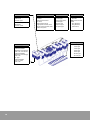
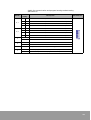
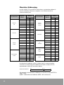
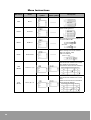
Contents
1. System Configuration ................................................. 7
NX70 Series PLC Features and System Configuration ............................... 7
Module Types and Combinations............................................................... 10
Programming Tools ..................................................................................... 14
2. Hardware Features and Specifications...................... 15
Overall Specifications .................................................................................. 15
Backplane...................................................................................................... 17
Processor Module ........................................................................................ 19
Power Supply Module ................................................................................. 24
I/O Modules................................................................................................... 26
3. Addressing Overview ................................................ 37
Double Word Addressing ............................................................................ 39
Absolute Addressing.................................................................................... 40
I/O Addressing .............................................................................................. 41
Special Registers .......................................................................................... 43
Timer/Counter Area...................................................................................... 50
Processor Operation Mode.......................................................................... 54
Processor Processing Procedure ............................................................... 55
4. Installations............................................................... 57
Power Supply Module Wiring ..................................................................... 59
Input and Output Wiring.............................................................................. 61
Terminal Block Type Module Wiring .......................................................... 68
Connector Type Module Wiring.................................................................. 69
Safety Measures........................................................................................... 73
NX70 Processor Module Communications Specifications ....................... 74
EEPROM Backup (for NX70-CPU70p1, NX70-CPU70p2) ........................... 75
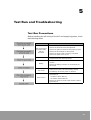
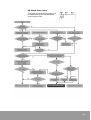
5. Test Run and Troubleshooting ................................. 77
Test Run Precautions ................................................................................... 77
Test Run Procedure...................................................................................... 78
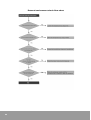
Test Run Flow Charts ................................................................................... 79
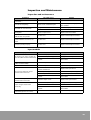
Inspection and Maintenance ....................................................................... 85
3
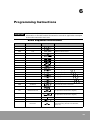
6. Programming Instructions......................................... 89
Basic Sequence Instructions ....................................................................... 89
Timer, Counter and Shift Register Instructions ......................................... 90
Comparison Instructions ............................................................................. 91
Substitution, Increment and Decrement Instructions ............................... 91
Arithmetic Instructions ................................................................................ 92
Logical Instructions ...................................................................................... 93
Rotation Instructions.................................................................................... 93
Word Conversion Instructions .................................................................... 94
Bit Conversion Instructions ......................................................................... 95
Move Instructions......................................................................................... 96
Program Control Instructions ...................................................................... 97
System Control Instructions........................................................................ 98
Communications Control Instructions........................................................ 99
7. Catalog Numbers and Dimensions .......................... 101
NX70 Product Catalog Numbers............................................................... 101
NX70 Product Dimensions ........................................................................ 106
Decimal, Bin, Hex, BCD, Gray Code Cross-reference Table.................... 109
ASCII Code Table........................................................................................ 110
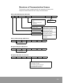
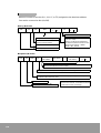
Appendix - Communication Protocols for NX70 ......... 111
Communication Protocols for NX70
(NX70-CPU70p1 and NX70-CPU70p2) ...................................................... 111
Communication Protocols ......................................................................... 112
Structure of Communication Frames ....................................................... 117
Communication Program Examples......................................................... 122
4
Safety Considerations
Please read this manual and the related documentation thoroughly
and familiarize yourself with the directions before installing, operating
or performing inspection and preventive maintenance. Make sure to
follow the directions correctly to ensure normal operation of the
product and your safety.
WARNING
• If this product is used in a situation that may cause
personal injury and/or significant product damage,
implement safety measures such as use of fault-safe
equipment.
• Do not use this product under the conditions
exposed to explosive gases. It may cause an
explosion.
ATTENTION
• Make sure to use an external device when
configuring the protective circuit breakers for
emergencies or interlock circuits.
• Fasten the terminal screws tightly to ensure that the
cable connection is secure. Incorrect cable
connection may cause overheat and product
malfunction.
• Operate and keep the product under the allowed
conditions directed in product specifications.
Otherwise it may cause overheating and product
malfunction.
• Do not disassemble or remodel the product.
Otherwise it may cause an electric shock or
malfunction.
• Do not touch the terminals when the power is on.
Otherwise it may cause an electric shock.
5
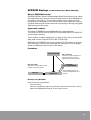
Installation Environment
ATTENTION
Do not install your PLC system if any of the following
conditions are present.:
• Ambient temperature outside the range of 0 to 55 °C
(32 to 131 °F).
• Direct sunlight.
• Humidity outside the range of 30% to 85% (noncondensing)
• Chemicals that may affect electronic parts.
• Excessive or conductive dust, or salinity.
• High voltage, strong magnetic fields, or strong
electromagnetic influences.
• Direct impact and excessive vibration.
ATTENTION
Electrostatic Discharges
Under dry condition, excessive electrostatic discharges
may occur. Make sure to remove electrostatic
discharges by touching a grounded metal piece before
touching your controller system modules.
ATTENTION
Cleaning
Never use chemicals such as thinner because they
melt, deform or discolor PCB boards.
ATTENTION
Precautions for use of power
• Run your PLC system only after the I/O devices and
motor devices have started. (For example, first
power on in the PROG mode, then change the
operation mode to RUN.)
• Make sure to power off I/O devices after ensuring
PLC operation is stopped.
• If you power on/off I/O devices when the PLC system
is in operation, the system may malfunction because
input signal noises may be recognized as normal
inputs.
ATTENTION
Before powering on
Make sure to follow these directions before powering
on your PLC system.
• When installing the system, ensure that there are no
metal chips or conductive fragments that stick to
wiring cables.
• Ensure that power supply and I/O wirings and power
supply voltage are all correct.
• Securely fasten installation and terminal screws.
• Set the operation mode switch to PROG mode.
6
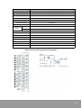
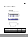
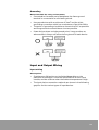
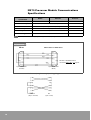
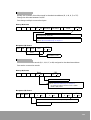
1
System Configuration
NX70 Series PLC Features and System
Configuration
System configuration
Communication cable
(NX_CBLCPU2)
NX70-CPU70p1
9.6k step base memory
1 port (RS232/RS485)
NX70-CPU70p2
20k step base memory
2 ports (RS232/RS485)
Computer (WinGPC)
Features
• High-speed processing
With the high-speed ASIC, the NX70 processes basic
instructions at a speed of 0.2 µs per step.
• Runtime Editing
The NX70 processor module allows you to modify instructions
while operating.
• Built-In Real Time Clock (RTC)
Built-in real time clock supports programming by time and date.
(Supported only for the NX70-CPU70p2 module.)
7
• High-capacity programming and memory backup
The NX70 module allows you to program up to 20K words for
NX70_CPU70p2, and 9.6k words for NX70_CPU70p1. Built-in
flash EEPROM allows you to save programs separately.
• Self-diagnostics
Self-diagnostics allows you to minimize system errors and
maximize diagnostic efficiency.
• Maximum 384 I/O points
With 12-slot processor module, you can use up to 384 I/O points
(with terminal block type, 192 points).
• Supports various I/O and specialty modules
The NX70 processor module supports 24V dc input (16/32
points), 110V ac input, 220V ac input, relay output, transistor
output (16/32 points), SSR output, A/D (4 channels), D/A (4
channels), RTD (4 channels), TC (4 channels), high-speed
counter, and SCU.
• WinGPC as programming tool
WinGPC, designed for processor control, lets you create,
modify, force I/O, download, and upload the program. It is a
powerful, easy-to-use programming tool.
• Various I/O base options (up to 12 slots)
NX series PLC allows you to choose a backplane from 2, 3, 5, 6,
8, 10, or 12 slots for maximum system configuration flexibility.
• Built-in RS232C/RS485, 2 ports (NX70-CPU70p2 module)
With two built-in communication ports, the CPU70p2 module
allows you to connect directly to computers or touch panels and
exchange a high volume of data at high speed. The COM2 port
supports a simple user-defined communication, and allows you
to connect to barcode readers, inverters, or servo motors.
(Binary communication is available.)
8
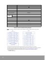
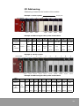
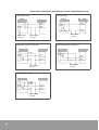
2-Slot Type
3-Slot Type
5-Slot Type
6-Slot Type
(NX70-BASE02)
32 Points: 16-point I/O
64 Points: 32-point I/O
(NX70-BASE02)
48 Points: 16-point I/O
96 Points: 32-point I/O
(NX70-BASE02)
80 Points: 16-point I/O
160 Points: 32-point I/O
(NX70-BASE02)
96 Points: 16-point I/O
192 Points: 32-point I/O
8-Slot Type
10-Slot Type
(NX70-BASE02)
128 Points: 16-point I/O
256 Points: 32-point I/O
(NX70-BASE02)
160 Points: 16-point I/O
320 Points: 32-point I/O
12-Slot Type
(NX70-BASE12)
192 Points: 16-point I/O
384 Points: 32-point I/O
Basic configurations and I/O
• Flexible system configuration: 7 types of backplane (2-, 3-, 5-, 6-,
8-, 10- and 12-slot)
The NX70 PLC has 7 types of backplane (2-, 3-, 5-, 6-, 8-, 10 and
12-slot type), providing you with very flexible I/O configuration.
All backplane, I/O, power supply, and specialty modules are
available regardless of processor type.
• Maximum 384 I/O points
With 12-slot NX70 PLC, you can use up to 384 I/O points (using
32-point module). With terminal block type, up to 192 points are
available (using 16-point module).
The backplane may have to be replaced when expanding the
number of modules.
9
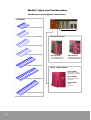
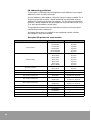
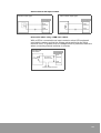
Module Types and Combinations
Combinations of backplane and modules
Backplane
2-slot type (NX70-BASE02)
3-slot type (NX70-BASE03)
Processor module
5-slot type (NX70-BASE05)
6-slot type (NX70-BASE06)
NX70-CPU70p2
20k step base memory
2 ports (RS232/RS485)
NX70-CPU70p1
9.6k step base memory
1 port (RS232/RS485)
8-slot type (NX70-BASE08)
Power supply module
NX70-POWER1
110 to 220V ac Input
3.5A at 5V, 0.3A at 24V
10-slot type (NX70-BASE10)
NX70-POWER2
110 to 220V ac Input
4.0A at 5V
NX70-PWRDC
24V dc
4.0A at 5V
12-slot type (NX70-BASE12)
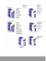
10
• 16-point output
module
• 32-point input
module
Relay OUT
(NX70-Y16R)
(NX70-Y16RV)
Transistor OUT
(NX70-Y16T)
SSR OUT
(NX70-Y16SSR)
24V dc IN
(NX70-X32D)
(NX70-X32D1)
I/O module
• 16-point input
module
24V dc IN
(NX70-X16D)
(NX70-X16D1)
110V ac IN
(NX70-X16A110)
220V ac IN
(NX70-X16A220)
• 8-point output
module
Relay OUT
(NX70-Y8R)
• 16-point input/
output module
• 32-point output
module
Transistor OUT
(NX70-Y32T)
(NX70-Y32P)
DC IN/Relay OUT
(NX70-XY16)
• 32-points input/
output module
DC IN/Relay OUT
(NX70-XY32)
• RTD input
module
Specialty module
• Analog input
module
4 channels
(NX70-RTD4)
4 channels,
• TC input
current/voltage input module
(NX70-AI4VC)
4 channels
(NX70-TC4)
• Analog output
module
• High-speed
4 channels, current
counter
output (NX70-AO4C)
2 channels
4 channels, voltage
(NX70-HSC2)
output (NX70-AO4V)
1 channel
2 channels, current
(NX70-HSC1)
output (NX70-AO2C)
2 channels, Voltage
output (NX70-AO2V)
• High-performance
high-speed
counter 4CH
4 channels
(NX70-HSC4)
• Pulse output *
module
4 channels
(NX70-PULSE4)
• MW-link module
(NX70-MWLINK)
Wire-Link
funchion
SCU module
(NX70-SCU)
11
Processor Module
NX70-CPU70p1
9.6k words
1 Comm. port
NX70-CPU70p2
20k words
2 Comm. ports
Specialty Module
I/O Module
Software & cable
A/D, D/A, RTD, TC, SCU
module
8-point/8-point
mixed type
Computer software
High-speed counter
(1/ 2CH)
16-point/16-point
mixed type
High-performance/
high-speed counter (4CH)
8-point type
PC communication
cable
Pulse output module (4CH)
32-point type
MW-link system
16-point type
- WinGPC
- NX_CBLCPU2,
NX_CBLCPU5
(NX70 CPU)
Backplane
Power Supply Module
AC Type
3-slot type
1) NX70-POWER1
(110/220V, free voltage)
3.5A at 5V, 0.3A at 24V
5-slot type
6-slot type
2) NX70-POWER2
(110/220V, free voltage)
4.0A at 5V
10-slot type
DC Type
1) NX70-PWRDC
(24V dc, Input)
4.0A at 5V
12
2-slot type
8-slot type
12-slot type
Limitations on current consumption
5V power supply
Internal 5V power is supplied to each module through backplane bus.
Power supply
module
24V
0.3A
None
Rated output
current
5V
24V
NX70-POWER1
3.5A
0.3A
NX70-POWER2
4.0A
None
NX70-PWRDC
4.0A
None
None
24V power supply
Input/Output module capacity
The power supply module supplies 24V
power to each I/O module. (limited
capacity)
Commercial 24V power supply
Supplies 24V power to each I/O module.
NOTE 1 The 24V power that the power supply provides can be used for all input/output modules that requires
24V. However, since there is a limitation on current capacity, we recommend you purchase 24V power supplies
separately according to your needs.
(NX70-POWER1: 0.3A at 24V)
(NX70-POWER2: No 24V output)
NOTE 2 For 24V power source to input/output module, you can use either 24V power supply module or a
commercial 24V power supply. However, do not connect them in parallel.
Use of internal and external power
• 5V internal power
The 5V dc power used for driving the internal circuit of each module
is supplied from the power supply module through the internal bus
of the backplane. (No separate power supply is required.)
• 24V power
The NX70-power1 24V dc power can be used for input power to
input modules and driving output circuits of output modules.
For additional 24V power, you may also have to use another power
supply module or a commercial power supply.
Do not connect together the NX70 power supply and a commercial
power supply in parallel.
The NX70-POWER2 or the NX70-PWRDC modules do not provide
24V power. (Only 5V output is provided.)
• Current consumption by each module
Give considerations to current consumption by each module so that
its power usage does not exceed the rated power usage at 5V or
24V dc.
13
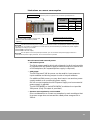
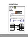
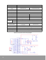
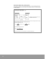
Programming Tools
Tools required for programming
The following tools are required when programming with WinGPC.
c
WinGPC software (for Windows)
d
e
c
Personal computer
d
WinGPC (for Windows)
WinGPC is the programming tool for editing and debugging PLC programs
for NX series controllers. WinGPC supports Microsoft Windows operating
system.
e
Cable for programming
For connection to the communication port of the NX70 processor module,
you can either purchase and use NX_CBLCPU2 or NX_CBLCPU5 cable or
construct the needed cables as follows:
Processor module
9-pin connector
14
Computer
9-pin connector
Signal
Pin No.
Pin No.
Signal
TXD
2
2
RXD
RXD
3
3
TXD
-
4
4
DTR
S.G
5
5
S.G
485(-)
6
6
DSR
485(+)
7
7
RTS
-
8
8
CTS
VCC
9
9
-
2
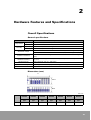
Hardware Features and Specifications
Overall Specifications
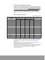
General specifications
Item
Temperature
Humidity
Specifications
Operating
0 °C to +55 °C (32 °F to 131 °F)
Storage
-25 °C to +70 °C (-13 °F to 158 °F)
Operating
30 to 85% RH (non-condensing)
Storage
30 to 85% RH (non-condensing)
Withstand voltage
1500V ac for 1 minute between external terminal (ac) and frame ground (FG)
500V ac for 1 minute between external terminal (dc) and frame ground (FG)
Insulation resistance
100 MΩ or more at 500 mega V dc between external terminal and frame ground
(FG)
Vibration immunity
10 to 55 Hz 1 sweep per minute, 0.75 mm peak to peak, 10 minutes per axis
(X, Y, Z)
Shock immunity
10G 4 times for each X, Y, Z direction
Noise immunity
1500 Vp-p with 50 ns to 1 µs pulse width (generated by noise simulator)
Environment
IP 20
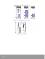
Dimensions (mm)
A
105.0
88.0
unit: mm
A (mm)
NX70BASE02
NX70BASE03
NX70BASE05
NX70BASE06
NX70BASE08
NX70BASE10
NX70BASE12
2-slot
type
3-slot
type
5-slot
type
6-slot
type
8-slot
type
10-slot
type
12-slot
type
149.5
185.0
256.0
291.5
362.5
398.0
433.5
15
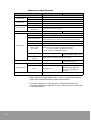
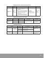
Performance specifications
CPU type
NX70-CPU70p1
Control method
Stored program, cyclic operation
External I/O
Instructions
Digital
384 points (32-point module/12 slots)
Analog
48 channels (4-channel module/12 slots)
Basic
28 types
Advanced
147 types
Basic instructions
Process speed
NX70-CPU70p2
Advanced
instructions
Program capacity
I/O (R)
Link contact (L)
Internal contact (M)
Keep contact (K)
Special contact (F)
0.2 µs per step
1.0 to several tens of µs per step
9.6k words
20k words
R0.0 to R127.15 (2,048 points)
L0.0 to L63.15 (1,024 points)
M0.0 to M127.15 (2,048 points)
(Note: Available as link contact for NX70-CPU70p2, 64 words)
K0.0 to M127.15 (2,048 points)
F0.0 to F15.15 (256 points)
256 channels (Timer + Counter), Set value range: 0 to 65535
Memory size
Timer/Counter
(TC or TIM)
Timer: 0.01 second: CH000 to CH063 (64 channels),
0.1 second: CH064 to CH255 (192 channels)
Counter: CH000 to CH255 (256 channels)
Data register (W)
Special register
(W, SR)
Real time clock
Port 2
Backup using flash ROM
W0000 to W2047,
W3072 to W5119 (4,096 words)
W256 (=SR000) to W3071 (=SR511) (512 words)
Not Applicable
Port 1
Communication
W0000 to W2047 (2,048 words)
Year, Month, Date, Hour,
Minute, Second, Day
Supports both RS232 and RS485, 4800/9600/19200/38400 bps
Not Applicable
Supports both RS232 and
RS485, 4800 to 38400 bps
Supports a user-defined
protocol
Supports all (built-in CPU module)
• Keep contact (K), data register (W), counter’s preset value register
retain their last values before power was removed.
• The super capacitor in the processor module backups all user
programs and specific registers for up to 48 hours, even in the event
of a power failure.
16
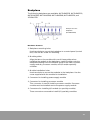
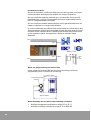
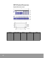
Backplane
The following backplanes are available: NX70-BASE02, NX70-BASE03,
NX70-BASE05, NX70-BASE06, NX70-BASE08, NX70-BASE10, and
X70-BASE12.
c
d
e
Example of 5-slot
backplane
(NX70-BASE05)
f
g
h
Hardware features
c Backplane mounting holes
Use these holes to mount the backplane to a control panel (control
box). Use the M5 screw for mounting.
d Module guides
Align the tab on the module with one of these guides when
installing the module to the backplane. Install modules onto the
backplane starting from the leftmost guide in the order of power
supply module, processor module, and I/O and/or specialty
modules.
e Module installation holes
Use these holes to secure the modules to the backplane. Use the
screw supplied with the module for installation.
f Connector for installing power supply module
g Connector for installing processor module
This connector is used to install a processor module. Processor
module must be installed next to the power supply module.
h Connectors for installing I/O module (or specialty module)
These connectors are used to install I/O (specialty) modules.
17
Types of backplane
18
Slot number
Catalog number
2
NX70-BASE02
3
NX70-BASE03
5
NX70-BASE05
6
NX70-BASE06
8
NX70-BASE08
10
NX70-BASE10
12
NX70-BASE12
Remarks
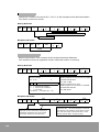
Processor Module
NX70-CPU70p1 processor module
(Bottom)
(Front)
(Side)
Hardware features
c Status LEDs
Display the operational status of the PLC such as the run, stop, error
and alarm status.
d Operation mode selector switch
Used to change the operation mode of the controller.
e RS232/RS485 communication port (9-pin COM port)
Used to connect to the programming tool (WinGPC) and/or touch
panel.
f Operating conditions setting switch
DIP switches for 6 poles, termination resistance setting, and
communication and program booting method selection.
g Backup battery for memory
Supplies a backup power to the built-in memory (RAM). The
connector is not connected at shipping.
19
Status LEDs
Status LEDs
LED
Color
Description
RUN
Green
On when the processor is running.
PROG
Green
On when the program can be edited.
COMM
Green
Flashing when the processor is communicating.
ERROR
Red
On when a processor error occurs.
BATT
Red
On when the battery is not mounted or is low.
Operation mode selector switch
Status
Description
RUN
Sets the processor operation mode to RUN mode.
RMT
Sets the processor operation mode to RUN or PROG mode.
PROG
Sets the processor operation mode to STOP mode, i.e., PROG mode.
Operating conditions setting switch
Pin No.
6
5
Pin
setting
OFF
OFF
Sets the communication speed to 9600 bps
ON
OFF
Sets the communication speed to 19200 bps
OFF
ON
Sets the communication speed to 38400 bps
ON
ON
Sets the communication speed to 4800 bps
OFF
Sets the communication method to RS-232C
communications.
ON
Sets the communication method to RS-485
communications.
OFF
When operating with the program stored in the built-in
RAM.
ON
When operating with the program stored in flash
ROM.
4
3
ON
ON
For RS-485 communication, set both pins 1 and 2 to
On if the system is an end-station.
OFF
OFF
For RS-485 communication, set both pins 1 and 2 to
Off if the system is not an end-station.
2, 1
20
Description
DIP
Switch
Remarks
Switches for
setting
communication
and program
booting methods
Switches for
termination
resistance setting
NX70-CPU70p2 processor module
(Bottom)
(Front)
(Side)
Hardware features
c Status LEDs
Displays the operational status of the PLC such as the run, stop,
error and alarm status.
d Operation mode selector switch
Used to change the operation mode of the controller.
e RS232/RS485 communication ports (9-pin COM1 and COM2 ports)
Used to connect to the programming tool (WinGPC), touch panel, or
MMI. Allows user-defined communication. (COM2 port).
f Operating conditions setting switch
DIP switch 1 (4 poles, termination resistance setting)
DIP switch 2 (8 poles, communication and program booting method
setting)
g Backup battery for memory
Supplies a backup power to the built-in memory (RAM). The
connector is not connected at shipping.
21
Status LEDs
LED
Color
Description
RUN
Green
On when the processor is running.
PROG
Green
On when the program can be edited.
COM1
Green
Flashing when the processor is communicating via COM1.
COM2
Green
Flashing when the processor is communicating via COM2.
ERROR
Red
On when a processor error occurs.
BATT
Red
On when the battery is not mounted or is low.
Operation mode selector switch
Status
Description
RUN
Sets the processor operation mode to RUN mode.
RMT
Sets the processor operation mode to RUN or PROG mode.
PROG
Sets the processor operation mode to STOP mode, i.e., PROG mode.
Operating conditions setting switch
Switch for termination resistance setting (DIP switch 1)
Pin No.
Pin
setting
ON
ON
For RS-485 communication, set both pins 3 and 4 to On if the system
is an end-station. (Enables termination for COM1 terminal)
OFF
OFF
For RS-485 communication, set both pins 3 and 4 to Off if the system
is not an end-station. (Disables termination for COM1 terminal)
ON
ON
For RS-485 communication, set both pins 1 and 2 to On if the system
is an end-station. (Enables termination for COM2 terminal)
OFF
OFF
For RS-485 communication, set both pins 1 and 2 to Off if the system
is not an end-station. (Disables termination for COM2 terminal)
3, 4
1, 2
22
Description
DIP Switch 1
Switch for communication and program booting method setting
(DIP switch 2)
Pin No.
8, 7
6, 5
4
3
2
1
Pin
setting
Description
OFF
OFF
Sets the communication speed on COM2 terminal to 9600 bps
ON
OFF
Sets the communication speed on COM2 terminal to 19200 bps
OFF
ON
Sets the communication speed on COM2 terminal to 38400 bps
ON
ON
Sets the communication speed on COM2 terminal to 4800 bps
OFF
OFF
Sets the communication speed on COM1 terminal to 9600 bps
ON
OFF
Sets the communication speed on COM1 terminal to 19200 bps
OFF
ON
Sets the communication speed of COM1 terminal to 38400 bps
ON
ON
Sets the communication speed on COM1 terminal to 4800 bps
ON
Selects RS-485 communications for COM1
OFF
Selects RS-232C communications for COM1
ON
Selects RS-485 communications for COM2
OFF
Selects RS-232C communications for COM2
OFF
Always set to Off. (Used for system setting)
ON
Loads the program from EEPROM (flash ROM) at power-on.
OFF
Operates the system with the program in RAM at power-on.
DIP Switch 2
23
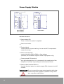
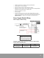
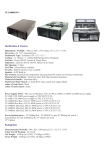
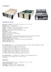
Power Supply Module
c
POWER
POWER
FUSE
USE ONLY
250V 1.5A
85-264
VAC
FUSE
USE ONLY
250V 1.5A
d
24V DC
f
FRAME
GROUND
24VDC
0.5A
OUTPUT
FRAME
GROUND
g
h
e
NX70-POWER1
NX70-POWER2
NX70-PWRDC
Hardware features
c Power status LED
Turns on when the power is supplied.
d Power fuse holder
e Terminal block
Terminal block for power wiring. You can use M3.5 compressed
screws for wiring.
f Power input terminal
Input terminal for 110V to 240V ac, free voltage.
(However, NX70-PWRDC supplies 24V dc input power only.)
g Frame ground (FG) terminal
As a grounding terminal, it is connected to the metal parts of the
backplane. Use class 3 grounding to avoid electrical shock.
h Power output terminal (24V dc)
Use this terminal when you need to supply 24V dc power to an I/O
module.
ATTENTION
24
Do not connect this power output terminal with other
commercial power supplies in parallel. It may cause
error or product malfunction.
Specifications
Catalog number
NX70-POWER1
NX70-POWER2
Rated input voltage
110 to 220V ac, free voltage
Allowable voltage range
85 to 264V ac
Input power frequency
47 to 63 Hz
47 to 63 Hz
Inrush current
20A or less
20A or less
Rated output current
4.0A at 5V
4.5A at 5V
Rated output current
0.3A at 24V
Not applicable
Catalog number
NX70-PWRDC
Rated input voltage
24V dc
Allowable voltage range
21.6 to 26.4V dc
Rated output current
4.5A at 5V
NOTE The power supply module supplies 5V power to all modules mounted onto the backplane.
Therefore, make sure that the current consumption of each module, which can use 5V power and/or 24V service
power, does not exceed the rated range.
ATTENTION
ATTENTION
NX70-POWER1 and NX70-POWER2 modules do not
guarantee protection against momentary power failure
at 110V ac.
Make sure that total current consumption of all
modules mounted on the backplane does not exceed
the rated current capacity of the power supply module.
• 5V power is supplied from the power supply module
mounted on the same backplane.
• The 24V control power is used for supplying a dc
power to I/O module.
• Do not connect this 24V control power with other
commercial power supplies in parallel. It may cause
error or product malfunction.
• A 250V 1A fuse is used for AC power. (The fuse is
built into the power supply module.)
• Be careful that the 24V side on the external terminal
does not exceed the current capacity. (It may cause
system errors.)
• NX70-POWER1 and NX70-POWER2 modules do not
guarantee protection against momentary power
failure at 110V ac.
25
I/O Modules
c
c
16-point type
d
f
e
16-point type
(Type A)
32-point type
(Type B)
32-point type
Hardware features
c I/O status LEDs
Displays the on/off state of I/O points.
d Terminal block (20 points)
Used for inputs, outputs and power supply wirings.
You can use M3.5 compressed screws for wiring.
For more information, refer to Terminal Block Type Module Wiring
on Chapter 4.
e Two 20-pin connectors (32 points)
Used as connectors for input/output contacts and power supply
wirings.
Use a flat cable or pin type harness.
For more information, refer to Connector Type Module Wiring on
Chapter 4.
f Terminal block cover
26
Input module specifications
Product name
Catalog number
DC input module
NX70-X16D
NX70-X16D1
Number of Input points
16 points
Insulation method
Photocoupler
Rated input voltage
12 to 24V dc
24V dc
Voltage range
10.2 to 26.4V dc
21.6V to 26.4V dc
Max. input current
10 mA or less
On voltage
9.6V or more
20V or more
Off voltage
2.5V or less
7V or less
Input impedance
Response
time
Approx. 3 KΩ
Off → On
2 ms or less
On → Off
2 ms or less
Internal current consumption
50 mA or less at 5V
Common method
8 points per COM
Status display
LED
External connection method
Terminal block (terminal screw: M3.0)
Suitable wire size
0.5 to 1.25 mm2
Weight
Approx. 160 g
Shape
Type A
Internal circuit and external wiring diagram
12V to 24V dc
(Note)
12V to 24V dc
(Note)
Note
* NC: No Connection
NOTE
The input voltage of NX70-X16D1 module is 24V dc.
27
Product name
DC input module
Catalog number
NX70-X32D
NX70-X32D1
Number of input points
32 points
Insulation method
Photocoupler
Rated input voltage
12 to 24V dc
24V dc
Voltage ranges
10.2 to 26.4V dc
21.6V to 26.4V dc
Max. input current
10 mA or less
On voltage/current
9.6V or more
20V or more
Off voltage/current
2.5V or less
7V or less
Approx. 3 KΩ
Input impedance
Response
time
Off → On
2 ms or less
On → Off
2 ms or less
Internal current consumption
90 mA or less at 5V
Common method
8 points per COM
Status display
LED
External connection method
Two 20-pin connectors
Suitable wire size
0.2 mm2
Weight
Approx. 130 g
Shape
Type B
Internal circuit and external wiring diagram
NOTE
The numbers in the picture below (1 to 20) indicate the numbers that are printed on the front of each
product.
[I]
12 to
24V dc
(Note)
XO
2
4
6
8
A
C
XE
COM1
COM2
[ II ]
1
2
3
4
5
6
7
8
9
10
11
12
13
14
15
16
17
18
19
20
12 to
24V dc
(Note)
XO
3
COM2
1
COM1
3
5
XF
7
D
8
B
B
9
D
7
XF
5
COM1
COM2
12 to
24V dc
(Note)
3
X1
5
7
9
11
13
15
17
19
2 COM2
4 COM1
XE
6
C
8
A
10
8
12
6
14
4
16
2
18
XO
20
12 to
24V dc
(Note)
NOTE The input voltage of the NX70-X32D1 module is 24V dc.
• The internal circuit is the same as that of the NX70-X16D module on the previous page.
• The (I) and (II) connectors are positioned in opposite directions. Please use caution prior to connecting.
• For external connection of the connector, please purchase a cable harness NX70_CBLDC and a Pin Type Ass'y
NX_PIN20. (For more information regarding the wiring methods, refer to Connector Type Module Wiring on
Chapter 4.
28
Product name
Catalog number
AC input module
NX70-X16A110
NX70-X16A220
Number of input points
16 points
Insulation method
Photocoupler
Rated input voltage
100 to 120V ac
200 to 240V ac
Voltage range
85 to 132V ac
170 to 264V ac
Max. input current
20 mA or less
On voltage/current
80V or less / 6 mA or less
160V or less / 6 mA or less
Off voltage/current
30V or more / 3 mA or more
50V or more / 3 mA or more
Input impedance
Approx. 15 KΩ
Approx. 20 KΩ
Response
time
Off → On
15 ms or less
On → Off
15 ms or less
Internal current consumption
80 mA or less at 5V
Common method
8 points per COM
Status display
LED
External connection method
Terminal block (terminal screw: M3.0)
Suitable wire size
0.5 to 1.25 mm2
Weight
Approx. 160 g
Shape
Type A
Internal circuit and external wiring diagram
100 to 120V ac
(Note)
NOTE
*NC: No Connection
The input voltage of NX70-X16D1 module is 24V dc.
29
Output module specifications
Product name
Relay output module
Catalog number
NX70-Y8R
Number of input points
8 points
NX70-Y16R
16 points
Insulation method
Photocoupler
Rated load voltage
250V ac, 30V dc
Load voltage range
85V to 264V ac
Max. load current
Response
time
NX70-Y16RV
3A per point
1A per point
Off → On
10 ms or less
On → Off
10 ms or less
External supply power
24V 150 mA or less
24V 150 mA or less
Surge protection circuit
Varistor
Internal current consumption
60 mA or less at 5V
100 mA or less at 5V
Common method
4 points per COM, 1 points per COM x 4
8 points per COM
Not applicable
Status display
LED
External connection method
Terminal block (terminal screw: M3.0)
Suitable wire size
0.5 to 1.25 mm2
Weight
Approx. 200 g
Shape
Varistor
Approx. 300 g
Type A
Internal circuit and external wiring diagram
NX70-Y16R: Without varistor
NX70-Y16RV: With varistor
NX70-Y8R
~
250V ac
30V dc
250V ac
30V dc
~
Varistor
240V
30
Product name
Transistor output module (NPN)
Catalog number
NX70-Y16T (NPN)
Number of input points
16 points
Insulation method
Photocoupler
Rated load voltage
12 to 24V DC
Load voltage range
10 to 30V AC
Max. load current
0.6A/point
Off state leak current
100 µA or less
Response
time
Off → On
1 ms or less
On → Off
1 ms or less
Internal current consumption
80 mA or less at 5V
Surge absorber
Zener Diode
Common method
8 points per COM (-)
Status display
LED
External connection method
Terminal block (terminal screw: M3.0)
Suitable wire size
0.5 to 1.25 mm2
Weight
Approx. 160 g
Shape
Type A
Internal circuit and external wiring diagram
COM(-)
YO-YF
12 - 24V DC(+)
12 to 24V dc
31
Product name
Catalog number
Transistor output module
NX70-Y32T (NPN)
NX70-Y32P (PNP)
Number of input points
32 points
Insulation method
Photocoupler
Rated load voltage
12 to 24V dc
Load voltage range
10 to 30V ac
Max. load current
0.4A/point
Off state leak current
100 µA or less
Response
time
Off → On
1 ms or less
On → Off
1 ms or less
Internal current consumption
140 mA or less at 5V
Surge absorber
Zener Diode
Common method
16 points per COM (-)
16 points per COM (+)
Status display
LED
External connection method
Two 20-pin connectors
Suitable wire size
0.2 mm2
Weight
Approx. 120 g
Shape
Type B
Internal circuit and external wiring diagram
NOTE
The numbers in the picture below (1 to 20) indicate the numbers printed on the front of a product.
[I]
[ II ]
• The (I) and (II) connectors are positioned in opposite directions. Please use caution prior to connecting.
• For external connections of the connector, please purchase cable harness NX70_CBLDC and Pin Type Ass'y NX-PIN20.
(For more information regarding the wiring methods, refer to Connector Type Module Wiring on Chapter 4).
• When wiring NX70-Y32P, please be cautious that the pins in the diagram picture and below are different.
- Pin #17, #18: - (VDC-)
- Pin #19, #20: COM (VDC+)
32
Product name
SSR output module
Catalog number
NX70-Y16SSR
Number of Input points
16 points
Insulation method
SSR
Rated load voltage
100 to 240V ac
Load voltage range
85 to 264V ac
Max. load current
0.5A/point
Off state leak current
100 µA or less
Response
time
Off → On
1 ms or less
On → Off
0.5 cycle + 1 ms or less
Internal current consumption
250 mA or less at 5V
Rated fuse
3A
Common method
8 points per COM
Status display
LED
External connection method
Terminal block (terminal screw: M3.0)
Suitable wire size
0.5 to 1.25 mm2
Weight
Approx. 300 g
Shape
Type A
Internal circuit and external wiring diagram
Fuse
AC100 ~ 240V
33
Product name
Mixed module of DC input/Relay output
Catalog number
NX70-XY16
Number of I/O points (16
points)
8 inputs (DC input)
8 outputs (Relay output)
Insulation method
Photocoupler
Rated input voltage
12 to 24V dc
Voltage range
10.2 to 26.4V dc
Max. input current
10 mA or less
Rated load voltage/current
250V ac, 30V dc, 1A/point
On voltage/current
9.6V or less/4mA or less
Off voltage/current
2.5V or less/1.5mA or less
Input impedance
Approx. 3 KΩ
External supply power
Not applicable
Response
time
24V 150 mA or less
Off → On
10 ms or less
On → Off
10 ms or less
Internal current consumption
Common method
80 mA or less at 5V
8 points per COM (both + and - polarity
are available)
Status display
LED
External connection method
Terminal block (terminal screw: M3.0)
Suitable wire size
0.5 to 1.25 mm2
Weight
Approx. 220 g
Shape
Type A
Internal circuit and external wiring diagram
12 to24V dc
250V ac
30V do
24V dc
34
8 points per COM
Product name
Mixed dc input/transistor output module
Catalog number
Number of I/O points
(32 points)
NX70-XY32
16 inputs (DC input)
16 outputs (TR output, NPN)
Insulation method
Photocoupler
Rated input voltage
12 to 24V dc
Voltage range
10.2 to 26.4V dc
Max. input current
10 mA or less
Rated load voltage/current
10 to 30V ac, 0.4A/point
On voltage/current
9.6V or less / 4 mA or less
Off voltage/current
2.5V or less / 1.5 mA or less
Input impedance
Approx. 3 KΩ
Surge absorber
External supply power
Response
time
Zener Diode
Not applicable
24V 150 mA or less
Off → On
10 ms or less
1 ms or less
On → Off
10 ms or less
1 ms or less
Internal current consumption
Common method
120 mA or less at 5V
16 points per COM (both + and polarities are available)
16 points per COM (-)
Status display
LED
External connection method
Two 20-pin connectors
Suitable wire size
0.2 mm2
Weight
Approx. 120 g
Shape
Type B
Internal circuit and external wiring diagram
16 inputs (DC input)
16 outputs (TR output)
For external connections of the connector, please purchase cable harness NX70_CBLDC and Pin Type Ass'y NX-PIN20.
(For more information regarding the wiring methods, refer to Connector Type Module Wiring on Chapter 4).
35
36
3
Addressing Overview
Addressing Overview
All the memory used for external I/O processing and internal data
processing has always both address and data (the content).
Addressing space is classified as R, L, M, K, F, TC, and W. These letters
are used to designate a specific area in memory as shown in the
following table.
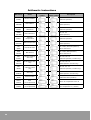
Memory areas
Addresses
Description
R0.0 to R127.15
• Local I/O memory area that can be set when configuring
I/O module.
• 2048 points, 128 words
R0.0 to R127.15
• Remote I/O memory area
• 2048 points, 128 words
L0.0 to L63.15
• Link contact sharing memory area, 1024 points,
Loop 0
• Internal contact can be used when you do not use the
link.
M0.0 to M63.15
• Link contact sharing memory area, 1024 points, Loop 1
Internal contact (M)
M0.0 to M127.15
• Internal auxiliary contact memory area
• 2048 points, 128 words
Keep contact (K)
K0.0 to K127.15
• Retentive internal auxiliary contact memory area
• 2048 points, 128 words
• Cleared when downloading a program.
Special contact (F)
F0.0 to F15.15
• Special internal contact memory area
• 256 points, 16 words
Timer/Counter (TC)
TC000 to TC255
SV000 to SV255
PV000 to PV255
Data register (W)
W0 to W2047
• Area that retains the data in case of power failure
• Bits are not addressable
• Cleared when downloading program
Special register
(SR)
W3072 to W5119
SR000 to SR511
• Special internal data area for CPU status and RTC
External I/O area (R)
Link contact (L)
•
•
•
•
256 channels common use (timer, counter)
TC is contact signal.
SV is Set Value, PV is Present Value.
SV can hold values from 0 to 65535.
37
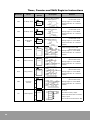
The R, L, M, K, F, and TC areas can be used for both bit and word
addressing. The W area can be used to process word data only. The
L area can be used as internal contacts. Keep contact (K), data register
(W), and counter's preset value register retain their last values before
power was removed. Cleared when a new program is downloaded.
A bit address is composed of a character (R, L, M, K, F) that identifies
its type, a five digit word address (0.0 to 127.15, increases by 0 to 15).
The timer/counter contact is represented by the TC label followed by
three digits. The three digits indicate the channel number of the timer/
counter (TC000 to TC255). TIM000 indicates a contact instead of TC000
for PGM10 and PGM-500.
A word address is composed of a character (R, L, M, K, W) and a four
digit number (0000 to 2047). Special registers have alternative address
representation. Special registers SR000 to SR511 can be also
represented as W2560 to W3071.
Both of bit and word addresses can be used to address the memory
areas of R, L, M, K. However, be cautious that instructions use a
specific type of address, either bit or word address, and the used
addresses are resolved automatically depending on the type of
instruction.
A bit can have the content of either On (1) or Off (0) state. A word is
composed of 16 bits and holds a data value from 0 to 65,535. A double
word is composed of 32 bits and holds a data value from 0 to
4,294,967,295.
Expression example
R
1 2 3
●
1 2
Bit number
1- or 2-digit, range is 00 to 15 increase as a
decimal module.
Word number
When used with a bit number, 3 digits (000 to 127) are
used.
When used as a word number only, it is expressed in
4 digits (0000 to 3071), and increases as a decimal
module and omits the bit number.
Address type
Depending on the type of the address, it is distinguished into
R, L, M, K, F, or W.
The W area contains:
data area (W0000 to W2047),
timer set value area (W2048 to W2303 = SV000 to SV255),
timer present value area(W2304 to W2559 = PV000 to PV255),
and special register (W2560 to W3071 = SR000 to SR511).
38
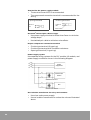
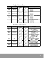
Double Word Addressing
Double word addressing is same with word addressing, except that
32-bit data is referenced by the specified address and its next address.
The type of instruction used determines which addressing, word or
double word addressing, is applied. For comparison instructions, the
programmer must be in “Double Mode” to enter a double-word
comparison. For other instructions, those instructions that start with a
D in front of the related word instruction are double word instructions,
and the data is processed as double words
Example 1:
LET
D=W0
Word
W0 is processed as 16-bit (1 word) data.
(0 to 65, 355)
S is processed from 0 to 65,535.
S=7000
DLET
D=W0
Double
word
Double word W0 is composed of W0 and W1.
W0 is LSB. W1 is located in MSB.
W0000 is
S=70000
2
31
15
2
30
14
…
2
…
1
… … …
W0001
17
2
0
16
2
15
15
2
14
14
…
2
…
2
2
2
1
1
2
0
0
… … …
W0000
The value of D or S of the instruction can process data from 0 to 4,294,967,295.
Example 2:
M1
MO
M1
M2
M3
M0
Range when double word instructions are used
M2
39
Absolute Addressing
In LDR, DLDR, STO, and DSTO instructions, an absolute address is
used to indirectly reference a register or to utilize the built-in
communication port.
Classification
Register
address
Absolute
address
Dec.
Hex.
R0
0
0000
R1
1
0001
External
R2
2
0002
I/O
…
…
…
R126
126
007E
R127
127
007F
L0
128
0080
L1
129
0081
L2
130
0082
…
…
…
L62
190
L63
Link area
Internal
contact
Internal Keep
contact
Absolute
address
Register
address
Classification
Dec.
Hex.
F0
448
01C0
F1
449
01C1
F2
450
01C2
…
…
…
F126
462
01CE
F127
462
01CF
W0
512
0200
W1
513
0201
W2
514
0202
00BE
…
…
…
191
00BF
W2046
2558
09FE
M0
192
00C0
W2047
2559
09FF
M1
192
00C1
SV000
2560
0A00
M2
194
00C2
SV001
2561
0A01
M3
195
00C3
…
…
…
…
…
…
SV255
2815
0AFF
M126
318
013E
M127
319
013F
PV000
2816
0B00
K0
320
0140
PV001
2817
0B01
K1
321
0141
…
…
…
K2
322
0142
PV255
3071
0BFF
K3
323
0143
SR000
3072
0C00
…
…
…
SR001
3073
0C01
K126
446
01BE
…
…
…
K127
447
01BF
SR511
3583
0DFF
Special
Internal
contact
Data area
T/C
set value
T/C
present
value
Status
An absolute bit address, which is often used in communication,
consists of an absolute word address and a bit number (0 to 15,
represented as $0 to $F) as shown below.
absolute bit address
15
4
absolute word address
3
0
bit number
For example, the absolute bit address for internal contact K127.12 is
$1BFC (hex).
($1BFC = absolute word address $01BF + bit number $C)
40
I/O Addressing
Addressing is based on the location of the module.
Empty slot
Example 1: 8-slot system
Slot number
0
1
Input
16 points
2
Input
16 points
3
4
5
Input
32 points
Output
16 points
6
Input
32 poin0ts
7
Output
32 points
Output
32 points
Example of addressing for the system shown above
Slot
number
00
01
02
04
05
06
07
R0
R1
R2
R3 to R4
R5 to R6
R7 to R8
R9 to R10
R0.0
R0.1
R1.0
R2.0
R3.0
R5.0
R7.0
R9.0
R1.1
R2.1
R3.1
R5.1
R7.1
R9.1
~
~
~
~
~
~
~
R0.15
R1.15
R2.15
R4.15
R6.15
R8.15
R10.15
Word
address
Bit
address
Processor
module
03
Empty
slot
Example 2: 10-slot system
Slot number
0
Input
16 points
1
Input
16 points
2
Input
16 points
3
Output
16 points
4
Output
16 points
5
6
7
8
Input
32 points
Input
32 points
Input
32 points
Output
32 points
9
Output
32 points
Example of addressing for the system shown above
Slot
number
00
01
02
03
04
05
06
07
08
09
Word
address
R0
R1
R2
R3
R4
R5 to
R6
R7 to R8
R9 to
R10
R11 to
R12
R13 to
R14
R0.0
R1.0
R2.0
R3.0
R4.0
R5.0
R7.0
R9.0
R11.0
R13.0
R0.1
R1.1
R2.1
R3.1
R4.1
R5.1
R7.1
R9.1
R11.1
R13.1
~
~
~
~
~
~
~
~
~
~
R0.15
R1.15
R2.15
R3.15
R4.15
R6.15
R8.15
R10.15
R12.15
R14.15
Bit
address
CPU
module
41
I/O addressing guidelines
The processor automatically distinguishes input address from output
address for each module mounted.
A word address is allocated to a 16-point input or output module. For a
32-point mixed I/O module, 2 word addresses are allocated, a word
address for inputs and another for outputs. For the 16-point mixed I/O
module, 2 word addresses are allocated but only the lower 8 bits (0 to
7) of each word address can be used.
The modules mounted into the slots that are closer to the processor
module have lower addresses.
An empty slot means no module is mounted and a blank module
(NX-DUMMY) may be installed.
Occupied I/O points for each module
Module
Input module
Output module
Mixed I/O module
Occupied I/O points
NX70-X16D
16 points
NX70-X16D1
16 points
NX70-X32D
32 points
NX70-X32D1
32 points
NX70-X16A110
16 points
NX70-X16A220
16 points
NX70-Y8R
8 points
NX70-Y16R
16 points
NX70-Y16RV
16 points
NX70-Y16T
16 points
NX70-Y32T
32 points
NX70-Y32P
32 points
NX70-Y16SSR
16 points
NX70-XY16
32 points
32 points
NX70-XY32
MW-link module
NX70-MWLINK
0 points
SCU module
NX70-SCU
32 points
A/D module (4 channels)
D/A module (2 channels)
D/A module (4 channels)
NX70-AI4V
NX70-AI4C
64 points or 16 points
NX70-AO2V
32 points or 16 points
NX70-AO2C
32 points or 16 points
NX70-AO4V
64 points or 16 points
NX70-AO4C
64 points or 16 points
RTD module (4 channels)
NX70-RTD4
64 points or 16 points
TC module (4 channels)
NX70-TC4
64 points or 16 points
High-speed counter
42
Catalog number
NX70-HSC1
NX70-HSC2
32 points
High-performance high-speed counter
NX70-HSC4
64 points
Pulse output module
NX70-PULSE4
64 points
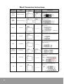
Special Registers
Word registers F000 to F15
Address
Function
Description
Remarks
F0 register
System check/control
F1 register
System check/clock
F2 register
Link control
Link installation and operation mode setting
Loop #0
F3 register
Link control
Link installation and operation mode setting
Loop #1
F4 register
Link status flag
Link participating station information
Loop #0
F5 register
Link status flag
Link participating station information
Loop #1
F6 register
Link status flag
Link data receiving information flag
Loop #0
F7 register
Link status flag
Link data receiving information flag
Loop #1
F8 register
Remote control flag
Remote operation control flag
Loop #0
F9 register
Remote control flag
Remote operation control flag
Loop #1
F10 register
Remote control flag
Remote operation control flag
Loop #2
F11 register
Remote control flag
Remote operation control flag
F12 register
User-defined
communication flag
For port COM2
F13 register
System reservation
F14 register
PID control
PID operation mode and operation/stop
control flag
Channel 0, 1, 2, and 3
F15 register
PID control
PID operation mode and operation/stop
control flag
Channel 4, 5, 6, and 7
System self-check/program checking,
operation control
0.01/0.02/0.1 ms timer output, calculation
results, carry flag
User-defined communication control flag
43
Word register F000 (F0.0 to F0.15)
Only a bit process is available.
44
Address
Function
Description
Normal status
F0.0
System check
When the power is applied, the system self-checks the
ROM. Should any fault exist, the error lamp is turned on.
Output and operation are halted.
OFF
F0.1
CPU ROM check
When the power is applied, the system self-checks the
ROM. Should any fault exist, the error lamp is turned on.
Output and operation are halted.
OFF
F0.2
CPU RAM check
When the power is applied, the system self-checks the
RAM. Should any fault exist, the error lamp is turned on.
Output and operation are halted
OFF
F0.3
User program
memory error
If the user program memory is damaged or the program is
faulty, the error lamp is turned on. Output and operation
are halted.
OFF
F0.4
Program syntax
error
The CPU initially runs and checks the user program’s
syntax. In the case of an error, the error lamp is turned on.
Output and operation are halted.
OFF
F0.5
Module range
error
Indicates an invalid R word (>64) used.
OFF
F0.6
Module change
error
On when an I/O module is removed/added/fails while the
system is running. The error lamp is on and the CPU keeps
running. Turned off when the error is corrected.
OFF
F0.7
Module type error
On when the I/O module information that is stored in the
CPU and module that is installed are different types, the
error lamp is turned on. Operation stops.
OFF
F0.8
Input data control
Off when the running CPU input module’s data is not
updated. (Input update is turned Off.)
ON
F0.9
Output data
control
Off to suspend updating of the output modules while the
CPU is in the Run state. (Output update is turned Off). The
outputs are maintained in their last valid state prior to
update being disabled.
ON
F0.10
All output off
Turns all outputs off while CPU is in the Run state.
(Outputs are disabled)
ON
F0.11
Constant cycle
interrupt
On when the constant cycle interrupt instructions are used.
(Refer to the INT instructions.)
(The cycle time is defined by the user.)
OFF
F0.12
Watchdog error
On when a scan time exceeds the watchdog set time.
OFF
F0.13
Disable module
type checking
On when the CPU starts the initial Run and the program is
checked without performing I/O module type verification.
F0.14
Program changes
during running
On when a user corrects the program while in Run mode. If
there are any syntax errors, the CPU is stopped.
F0.15
Run state control
On when the CPU is in the Run state. Off when stopped or
paused.
ON
Word register F1 (F1.0 to F1.15)
Only a bit process is available.
Address
Function
Description
Remarks
F1.0
First single scan
Maintain On state for first single-scan period, when the CPU
shanges its status stop to Run.
F1.1
Scan clock
F1.2
0.02-second clock
F1.3
0.1-second clock
Cycle On/Off state for each scan during the program.
(1Scan On, 1Scan Off)
10 ms: On, 10 ms: Off
10m S
10m S
10m S
50m S
50m S
50m S
5 00m S
5 00m S
5 00m S
50 ms: On, 50 ms: Off
500 ms: On, 500 ms: Off
F1.4
1-second clock
F1.5
Instantaneous
interrupt
F1.6
CPU running
status
On when the CPU is in the run state.
F1.7
Keep area
error display
On when the K retentive data is destroyed and/or changed.
F1.8
Carry flag
On in the event of carry when performing math instruction.
F1.9
Division
by zero error
F1.10
Range designation
error
F1.11
Reserved
System use area
F1.12
W area error
indication
System use area
F1.13
Reserved
System use area
Do not use
F1.14
Reserved
System use area
Do not use
F1.15
Reserved
System use area
Do not use
On when power is off for 20 ms or more.
Maintained
On when the denominator of division commands is zero.
On when the absolute address exceeds the specified range.
Do not use
NOTE The 16 bits in the F1 address provide the CPU’s special function and self-diagnosis result. They are used for
status contacts only, and are not used to modify or control the PLC. Only the F1.5 instantaneous interrupt display contact
should be used as an output contact by the user, to be turned off after power loss indication. NOTE
45
Word register F12 (F12.0 to F12.15)
Only a bit process is available.
Address
Function
F12.0
RTC check
F12.2
Description
Remarks
On when the RTC is enabled.
-
Flash
On when the 9.6 KW of flash memory is installed.
-
F12.3
Flash
On when the 16 KW of flash memory is installed.
-
F12.5
Battery error
On when the battery is not connected or the voltage is
lower than the backup voltage.
-
F12.7
Periodical scan
error
F12.10
RTC set error
F12.11
On when any error exists in the periodical program.
On when there is an error setting the RTC.
Output
Saving Flash and
checking boot
Off when the program is normally saved into Flash by
setting F12.15 On.
Output
F12.12
EEPROM backup
check
On when the program in EEPROM is the same with that in
RAM.
F12.13
RTC Set 1
On when you change the year, month, day, or date. Off
when the data set is normal.
I/O
F12.14
RTC Set 2
On when you change the hour, minute, or second. Off
when the data set is normal.
I/O
F12.15
Saving Flash
On when you save the current program into the flash. Off
when the data set is normal.
I/O
Special registers SR0 to SR016 (W2560 to W2576)
May be modified - each is composed of 1 word.
Address
Function
SR000
CPU ID number
Description
Indicates the CPU ID number in the lower 8 bits. 0 to 223 are the valid userdefined values, 255 is the default value.
Indicates current CPU information state. (run/stop/remote control/error)
←
MSB
SR001
CPU state
03
02
01
00
Error = 1
CPU run control (same as F0.15)
CPU switch remote control (REM) =1
CPU switch RUN = 1
CPU switch STOP= 0
46
SR2
Watchdog time
Indicates the user program watchdog time (unit: msec)
SR3
Scan time
SR4
Max. scan time
SR5
to SR7
Link module
number
SR8
PID table
PID register block start address
SR9
to SR10
Reserved
System use area
SR11
to SR16
Remote I/O
information
Indicates the scan time when executing a program. Updated at every scan
(unit: msec)
Indicates maximum value of scan time when executing a program.
Link module number as set by the link # 1, 2, 3
Remote setup area
Special registers SR017 to SR511 (W2577 to W3071)
May be changed - each is composed of 1 word.
Address
Function
Description
Gives result of self-diagnosis by CPU. Indicates error content .
MSB
SR017
System error
information
←
7
6
5
4
3
2
1
0
Watchdog time error = ON
Undefined instruction = ON
Peripheral device fault = ON
Misc. logic faults = ON
Logic circuit fault = ON
Microcomputer fault = ON
SR018
Location of
undefined
instruction
SR019
Reserved
SR020
Multiplication
SR021
Lower remainder
Stores the low order bit values of remainder after a division instruction has
been executed.
SR022
Higher
remainder
Stores the high order bit values of the remainder after a division instruction
has been executed.
SR023 to
SR027
Reserved
System use area
SR028 to
SR029
Defective slot
information
SR030 to
SR48
Reserved
SR49 to SR79
Slot information
Stores slot information for installed I/O modules.
SR261 to
SR279 *
Remote control
domain
Contains remote I/O configuration data.
SR289 to
SR297
RTC
SR298 to
SR373 *
User-defined
communication
area
SR374 to
SR379 *
Link error
information
SR380 to
SR511
Reserved
Indicates the location of the instruction (the step number) that caused an
undefined instruction error during program execution.
System use area
Stores high order bit values upon executing 16 bit multiplication instructions.
Location of defective slots mounted onto the basic slot
System use area (syntax information and system information)
Contains real time clock information
(year, month, day, hour, minute, second, date).
For port COM2
User-defined communication area
Link error information data.
System use area
* Applied when using communication modules
47
Program syntax error status register SR30 (W2590)
Indicates the result of the automatic check on the user program syntax
when the programmer or GPC executes a syntax check, and when the
operation mode is switched from the Stop state to the Run state. If the
value of W2590 is not zero, F004 bit turns On. The error lamp also turns
On.
Error correction method:
Find the error in the CPU online mode and then correct the program.
Word
SR30
48
Bit
Description
0
On if the I/O number range of bit process instruction is beyond the specified range or
designates an external contact/output module which is not installed.
1
On if the channel number of the timer or the counter exceeds 255 or is duplicated.
2
On if the bit or word number in the advanced instruction is beyond the specified range or if
it designates a module which is not installed.
3
On if a word number in the refresh instruction (INPR, OUTR) is beyond the specified range,
or if it designates a module which is not installed.
4
On if an undefined instruction exists.
5
On in event of a user program memory writing error.
6
On in event of miscellaneous errors.
7
On if the user program memory is abnormal.
8
On if an error on external I/O address and bit/word/double word numbers used occurs. For
example, the first slot is set with an input module and OUT R00001 is designated.
9
On if the label numbers of the JMP or CALL instructions exceed 63, the corresponding
instruction LBL or SBR does not exist, and/or the corresponding LBL/SBR instructions exist
prior to JMP/CALL instructions.
10
On if the label number of the LBL instruction exceeds 63 and/or is duplicated.
11
On if the JMPS/JMP instructions are mistakenly combined and/or used.
12
On if the FOR/NEXT instructions are mistakenly combined and/or used more than four
times. (Loop)
13
On if SBR/RET instructions are not combined and/or used and/or the SBR instructions
overlap or exceed 63.
14
On if NT/RETI instructions are not combined and/or used and/or more than two sets of INT
instructions are used.
15
On if no END instruction inserted automatically.
Real-time clock registers SR289 to SR297
(W2849 to W2857)
Sets the time of the built-in clock (RTC) and stores and displays the
present time. Data is stored in BCD format.
( ○ : bit = 0; ×: bit change)
Address
Classification
Details
Current
time
Time
setting
Bit address
15
14
13
12
11
10
9
8
7
6
5
4
3
2
1
0
○
×
×
×
×
×
×
○
○
○
○
○
×
×
×
Adjustment/
indication
SR289
Year
(4-digit BCD)
SR290
Date: day
○
SR291
Year: month
○
×
×
×
×
×
×
×
○
○
○
×
×
×
×
×
SR292
Second: 00
○
○
×
×
×
×
×
×
○
○
○
○
○
○
○
○
SR293
Hour: minute
○
○
×
×
×
×
×
×
○
○
○
○
○
○
○
○
SR294
Date: day
○
○
×
×
×
×
×
×
○
○
○
○
○
×
×
×
SR295
Year: month
○
×
×
×
×
×
×
×
○
○
○
×
×
×
×
×
SR296
Second: 00
○
○
×
×
×
×
×
×
○
○
○
○
○
○
○
○
SR297
Hour: minute
○
×
×
×
×
×
×
○
○
○
○
○
○
○
○
○
* Usable for NX70-CPU70p2 module only
In SR289, the year can be read in a 4-digit BCD.
Ex) $1998=1998, $2000=2000
SR289 to SR297 for clock functions are shown in BCD, so it is convenient to confirm in HEX.
NOTE
Set the range as follows:
Year: 00 to 99, Month: 01 to 12, Day: 01 to 31, Day of Week: 01 to 07 (Sun. to Sat.)
Hour: 00 to 23, Minute: 00 to 59, Second: 00 to 59
1. Ladder setting method:
For example, current date and time are: Tuesday, March 21, 1996, 18:35:07
Designate year, month, day
Designate hour, minute, second
Date indicators are
Sun (01), Mon (02), Tue (03),
Wed (04), Thu (05), Fri (06),
and Sat (07)
2. When changing the year, month, date, or day, new data is input in SR295, SR294, then the F12.14 bit is turned
On. The F12.10 bit is kept Off.
3. When changing the hour, minute, and second, new data is input in SR297, SR296, then the F12.14 bit is turned
on. If the new data is not set correctly, the F12.10 bit turns on.
4. The display date and set value are expressed in BCD so it is convenient to input as hex ($).
5. The year, month, and day are automatically changed.
49
Timer/Counter Area
Timer/counter set value and present value addresses
Channel
0
1
2
3
4
5
6
7
8
9
10
11
12
13
14
15
16
17
18
19
20
21
22
23
24
25
26
27
28
29
30
31
32
33
34
35
36
37
38
39
Set
value
(SV)
W2048
W2049
W2050
W2051
W2052
W2053
W2054
W2055
W2056
W2057
W2058
W2059
W2060
W2061
W2062
W2063
W2064
W2065
W2066
W2067
W2068
W2069
W2070
W2071
W2072
W2073
W2074
W2075
W2076
W2077
W2078
W2079
W2080
W2081
W2082
W2083
W2084
W2085
W2086
W2087
Present
value
(PV)
W2304
W2305
W2306
W2307
W2308
W2309
W2310
W2311
W2312
W2313
W2314
W2315
W2316
W2317
W2318
W2319
W2320
W2321
W2322
W2323
W2324
W2325
W2326
W2327
W2328
W2329
W2330
W2331
W2332
W2333
W2334
W2335
W2336
W2337
W2338
W2339
W2340
W2341
W2342
W2343
Channel
40
41
42
43
44
45
46
47
48
49
50
51
52
53
54
55
56
57
58
59
60
61
62
63
64
65
66
67
68
69
70
71
72
73
74
75
76
77
78
79
Set
value
(SV)
W2088
W2089
W2090
W2091
W2092
W2093
W2094
W2095
W2096
W2097
W2098
W2099
W2100
W2101
W2102
W2103
W2104
W2105
W2106
W2107
W2108
W2109
W2110
W2111
W2112
W2113
W2114
W2115
W2116
W2117
W2118
W2119
W2120
W2121
W2122
W2123
W2124
W2125
W2126
W2127
Present
value
(PV)
W2344
W2345
W2346
W2347
W2348
W2349
W2350
W2351
W2352
W2353
W2354
W2355
W2356
W2357
W2358
W2359
W2360
W2361
W2362
W2363
W2364
W2365
W2366
W2367
W2368
W2369
W2370
W2371
W2372
W2373
W2374
W2375
W2376
W2377
W2378
W2379
W2380
W2381
W2382
W2383
Channel
Set value
(SV)
80
81
82
83
84
85
86
87
88
89
90
91
92
93
94
95
96
97
98
99
100
101
102
103
104
105
106
107
108
109
110
111
112
113
114
115
116
117
118
119
W2128
W2129
W2130
W2131
W2132
W2133
W2134
W2135
W2136
W2137
W2138
W2139
W2140
W2141
W2142
W2143
W2144
W2145
W2146
W2147
W2148
W2149
W2150
W2151
W2152
W2153
W2154
W2155
W2156
W2157
W2158
W2159
W2160
W2161
W2162
W2163
W2164
W2165
W2166
W2167
Present
value
(PV)
W2384
W2385
W2386
W2387
W2388
W2389
W2390
W2391
W2392
W2393
W2394
W2395
W2396
W2397
W2398
W2399
W2400
W2401
W2402
W2403
W2404
W2405
W2406
W2407
W2408
W2409
W2410
W2411
W2412
W2413
W2414
W2415
W2416
W2417
W2418
W2419
W2420
W2421
W2422
W2423
NOTE If you change the above registers while the program is running or program them incorrectly, errors or damage
may occur. Be sure you understand the programming procedures of the timer/counter thoroughly.
50
Channel
120
121
122
123
124
125
126
127
128
129
130
131
132
133
134
135
136
137
138
139
140
141
142
143
144
145
146
147
148
149
150
151
152
153
154
155
156
157
158
159
160
161
162
163
164
165
NOTE
Set
value
(SV)
W2168
W2169
W2170
W2171
W2172
W2173
W2174
W2175
W2176
W2177
W2178
W2179
W2180
W2181
W2182
W2183
W2184
W2185
W2186
W2187
W2188
W2189
W2190
W2191
W2192
W2193
W2194
W2195
W2196
W2197
W2198
W2199
W2200
W2201
W2202
W2203
W2204
W2205
W2206
W2207
W2208
W2209
W2210
W2211
W2212
W2213
Present
value
(PV)
W2424
W2425
W2426
W2427
W2428
W2429
W2430
W2431
W2432
W2433
W2434
W2435
W2436
W2437
W2438
W2439
W2440
W2441
W2442
W2443
W2444
W2445
W2446
W2447
W2448
W2449
W2450
W2451
W2452
W2453
W2454
W2455
W2456
W2457
W2458
W2459
W2460
W2461
W2462
W2463
W2464
W2465
W2466
W2467
W2468
W2469
Channel
166
167
168
169
170
171
172
173
174
175
176
177
178
179
180
181
182
183
184
185
186
187
188
189
190
191
192
193
194
195
196
197
198
199
200
201
202
203
204
205
206
207
208
209
210
211
Set
value
(SV)
W2214
W2215
W2216
W2217
W2218
W2219
W2220
W2221
W2222
W2223
W2224
W2225
W2226
W2227
W2228
W2229
W2230
W2231
W2232
W2233
W2234
W2235
W2236
W2237
W2238
W2239
W2240
W2241
W2242
W2243
W2244
W2245
W2246
W2247
W2248
W2249
W2250
W2251
W2252
W2253
W2254
W2255
W2256
W2257
W2258
W2259
Present
value
(PV)
W2470
W2471
W2472
W2473
W2474
W2475
W2476
W2477
W2478
W2479
W2480
W2481
W2482
W2483
W2484
W2485
W2486
W2487
W2488
W2489
W2490
W2491
W2492
W2493
W2494
W2495
W2496
W2497
W2498
W2499
W2500
W2501
W2502
W2503
W2504
W2505
W2506
W2507
W2508
W2509
W2510
W2511
W2512
W2513
W2514
W2515
Channel
212
213
214
215
216
217
218
219
220
221
222
223
224
225
226
227
228
229
230
231
232
233
234
235
236
237
238
239
240
241
242
243
244
245
246
247
248
249
250
251
252
253
254
255
Set value
(SV)
W2260
W2261
W2262
W2263
W2264
W2265
W2266
W2267
W2268
W2269
W2270
W2271
W2272
W2273
W2274
W2275
W2276
W2277
W2278
W2279
W2280
W2281
W2282
W2283
W2284
W2285
W2286
W2287
W2288
W2289
W2290
W2291
W2292
W2293
W2294
W2295
W2296
W2297
W2298
W2299
W2300
W2301
W2302
W2303
Present
value (PV)
W2516
W2517
W2518
W2519
W2520
W2521
W2522
W2523
W2524
W2525
W2526
W2527
W2528
W2529
W2530
W2531
W2532
W2533
W2534
W2535
W2536
W2537
W2538
W2539
W2540
W2541
W2542
W2543
W2544
W2545
W2546
W2747
W2548
W2549
W2550
W2551
W2552
W2553
W2554
W2555
W2556
W2557
W2558
W2559
•
Channel: The inherent number of the timer and the counter (numbers that are equivalent to 000 of TC000).
•
Set Value (SV): The designated value for the timer (to turn On) and the counter (number of times On) to start
operation.
•
Present Value (PV): Current processing value of the timer (elapsed time) and the counter (number of counts).
51
Address (register)
Address refers to the location of memory being used. It can refer to the
external I/O module and internal memory.
An address is categorized into 1 bit, 16 bits (word), or 32 bits (double
word).
Bit
A bit is the minimum module required for calculation. It can be either
On (1) or Off (0).
Byte
A byte is made up of 8 bits. It can hold data values from 0 to 255. In
base 16, or hexadecimal, a byte can be expressed as 0 to FF. You
cannot have a value greater than 255 when using one byte.
Word
A word is made of 16 bits. It can hold data values from 0 to 65,535. In
base 16 a word can be expressed as 0 to FFFF.
NX PLCs set R, M, K, F, and W areas into word areas and can be
processed without any separate measures.
Double Word
A double word is made of 32 bits. It can hold data values from 0 to
4,294,976,295. In base 16, a double word can be expressed as 0 to
FFFFFFFF. In the D32LT, a double word is made up of two consecutive
word addresses as follows:
Double word address = Start word address + Next word address.
Example: When using W003,
W003 (double word address) = W003 (start word address) + W004 (next word address)
Scan Time
The CPU follows a procedure in which it 1) reads the inputs, 2)
processes the ladder program, and 3) updates the outputs. It
continually repeats this process. This 3-step process is called a “scan,”
and the time it takes to complete this process is the “scan time.” In a
typical PLC application, most of the scan time is used to process the
program. When programming, keep in mind that the scan time will
increase as you increase the number of inputs and outputs and/or the
size of the program
Edge
An edge is defined as the point when an input changes state. For
example, a rising edge occurs during the very first scan after the input
has changed from Off to On. A falling edge occurs after the input has
changed from On to Off.
52
BCD (Binary Coded Decimal)
BCD is used to express a decimal digit (0 to 9) using 4 bits. Conversion
of BCD values can be done in hexadecimal calculations.
Example: 59 (BCD) = 59 (HEX), 32 (BCD) = 32 (HEX)
Flash ROM
It refers to a ROM (EEPROM) that stores programs. Since its contents
can be deleted periodically, it is frequently used for equipments that
deals with programs such as a PLC.
How to use a register
•
R (Relay) register (Can be bit, word or double word)
Indicates the external I/O register that directly connects to the
general I/O module
•
M (Memory) register (Can be bit, word or double word)
An internal bit memory address which supports the relay of logical
operations. It is used as a word or double-word variable for
general calculations and programs.
When the power of the PLC is turned off or the CPU has stopped,
the register value is reset to 0.
•
W (Word) register (Can be bit, word or double word)
Same usage as M registers. The value is preserved after the power
is turned off, but can be cleared by program downloads or special
command words.
NOTE Not used as a bit (register only for word use)
•
K (Keep) register (Can be bit, word or double word)
Used for general calculation programs. The value is preserved
after the power is turned off.
•
F (Flag) register (Only process bit)
These bit registers provide special application specific functions to
the programmer of the PLC. They are also used as system control
bits, providing Run/Stop control of the PLC.
•
When a calculation or input value exceeds 65,535 (FFFF)
Use a double word instruction that can store and calculate values
over 65,535 in the K, M, R, and W registers. When a double word
instruction is used, it can represent values up to 4,294,967,295 (232).
•
When you want to reload the contents or values that you worked
today
Use the K and W area. These are preserved unless specifically
erased. The W area is erased by special instructions or program
downloads.
•
When you need numerical expressions such as A+B=C, 34 × 45=D,
A1>C1.
Use the R, M, W, and K area. If you use the R area, you can refer to
and output calculated values in I/O modules.
53
•
For bit operations, such as setting, resetting, shifting, or rotating
Use the M, K, and R area. You cannot perform bit operations in the
W area.
•
When you want to refer to or modify the set value of the timer or
counter.
Refer to or modify W2048 to W2303 or SV0 to SV255.
•
When you want to refer to or modify the present value of the
timer or counter.
Refer to or modify the address area from W2304 to W2559 or from
PV0 to PV255. The value holds true in STOP (PROG.) state in this
area.
The present value (PV) of the counter is maintained even after the
power is off.
Processor Operation Mode
What is the Processor operation mode?
The processor has an external RUN/REMOTE/PROG switch. The PLC
performs a system check that determines the position of the switch.
The switch position determines which operating mode the PLC is in.
It can set to RUN, STOP, REMOTE, or ERROR mode.
RUN Mode (operating)
The PLC reads the external contact signals in Run mode and executes
the user program stored in RAM. The external outputs are updated
every scan according to program results.
STOP Mode
The user program is stopped and the external outputs are turned Off.
In the Stop mode, you may correct, delete or transfer the
program.(This is the only mode in which you can save a program in
flash memory.)
PAUSE Mode
A user program is operated at every scan and the I/O and result value
is maintained. This mode is used when checking and debugging a
program at every scan. This mode is similar to the Stop mode, but it
does not initialize data.
ERROR Mode
It occurs when the CPU module finds internal defects after running the
self-diagnoses. Functions are not executed normally in this mode.
When an error occurs, the CPU stops all programs and turns all output
off. When an Error mode occurs, the user should check the error code
and take appropriate measures. Then turn the power on or put the
mode conversion switch in Prog and press the Initialize Key to clear the
error.
54
Allowed Functions in Operation Modes
5=On, ◑ =Flashing, ● =Off
Operation mode
selector switch
Operation
mode
RUN
REMOTE
PROG
LED status
RUN LED
PROG LED
Program
change
Data
change
Initialize
switch is
enabled
Mode at power
off-on
RUN
5
●
Disallowed
Allowed
○
Run
STOP
●
Allowed
Allowed
○
Run
RUN
5
Allowed
Allowed
○
Run
PAUSE
◑
Allowed
Allowed
○
Pause
STOP
●
5
5
5
5
Allowed
Allowed
○
Stop
When the PROG.LED is on, you can change the user program.
The INITIALIZE switch clears errors when the mode switch is set to
PROG.
When the mode switch is set to REMOTE and power is switched from
Off to On, the previous mode of operation is restored.
When debugging the user program, the mode switch should be set to
REMOTE.
Processor Processing Procedure
Program processing procedure
Program
analysis
Peripheral device
signal processing
1 scan time
The diagram indicates the PLC
program processing procedure.
The CPU regularly repeats
procedure 1 through 5. This cycle
is called 1 scan time.
Forced I/O
Process I/O
Watchdog time -> 0
•
Program analysis
Executes the program from its first step to its final step and stores
the internal/external output in the working RAM.
•
Peripheral device signal processing
Stores data from the communication module or peripheral device
to the internal memory.
•
Forced I/O processing
Turns on/off forced I/O bits, if any.
•
I/O processing
Preserves the On/Off state of the external I/O and uses it as an
input in the next scan. (For accurate processing, input should
continue for more than 1 scan time.)
The processed program outputs are sent from internal memory to
the external memory.
55
•
Watchdog time initialization
The watchdog elapsed time value is set to 0. (This value is the
watchdog calculation point until the next scan.)
The following illustration shows the difference between the relay
board and PLC sequence processing. The relay carries out all
sequences simultaneously while the PLC processes sequentially
throughout the program.
Processing of relay sequence
(Parallel process)
56
Processing of PLC program
(Serial process)
57
4
Installation and Wiring
Installation
Installation space and environment
External dimensions (mm)
Unit: mm
Type of backplane
Catalog number
Size A
Size B
Size C
2-slot type
NX70-BASE02
149.5
129.5
115.5
3-slot type
NX70-BASE03
185.0
165.0
151.0
5-slot type
NX70-BASE05
256.0
236.0
222.0
6-slot type
NX70-BASE06
291.5
271.5
257.5
8-slot type
NX70-BASE08
362.5
342.5
328.5
10-slot type
NX70-BASE10
398.0
378.0
364.0
12-slot type
NX70-BASE12
433.5
413.5
399.5
57
Installation location
Be sure to maintain a sufficient distance from wiring ducts, and other
machines below and above the module for proper ventilation.
Do not install the modules stacked up or horizontally. Doing so will
prevent proper cooling of the module and cause overheating inside
the PLC (programmable controller).
Do not install the module above devices which generate heat such as
heaters, transistors or large scale resistors.
In order to eliminate any effects from noise emission, power wires and
electromagnetic devices should be kept at least 100 mm away from the
surfaces of the module. When installing the module behind the doors
of the operation panel, be especially careful to maintain these
distances.
Duct
Min.
50mm
100mm or more
Min.
Duct
50mm
Other
devices
Space for programming tool connection
Leave a space of at least 180 mm from the mounting surface for
programming tool connections and wiring.
Approx. 110mm
Programming Cable
Approx. 180mm
Avoid installing the module in the following conditions
58
•
Ambient temperature outside the range of 0 to 55 °C
•
Ambient humidity outside the range of 30 to 85% RH
Door
of
rack
•
Sudden temperature changes causing condensation
•
Inflammable or corrosive gases
•
Excessive airborne dust, metal particles, salinity
•
Benzene, thinner, alcohol, other organic solvents or strong alkaline
solutions such as ammonia or caustic soda
•
Excessive vibration or shock
•
Direct sunlight
•
Location near high-tension wires, high-voltage devices, power
cables, power devices, or other devices with generate large power
surges or electronic fields when starting and stopping (esp. if
within 100 mm)
Power Supply Module Wiring
Power supply module wiring
NX70 power supply module
Use 2mm2 twisted pair
cable or larger
Breaker
Use an isolation
transformer when effects
from noise are great.
Use 2mm cable or larger
for grounding
Power
FUSE
USE ONLY
250V 1.5A
85 - 264
VAC
FRAME
GROUND
2
Caution
24V DC
0.3A
OUTPUT
Control power (24V)
24V can be supplied to an I/O
Module.
Must avoid parallel connections with
other 24V power supply modules or
with other power supply modules.
The power supply voltage connected to the power supply module
must be within allowable limits.
Catalog number
Rated input voltage
Allowable voltage
Range
NX70-POWER1
NX70-POWER2
110 to 220V ac
85 to 264V ac
59
Terminal for the power supply module
•
The terminal screw M3.5 is recommended.
•
The compressed connection terminal is recommended for the
wiring.
Circular type terminal
Open type terminal
7.0mm or
less
7.0mm or
less
Φ 3.7 ~ Φ 4.3
Use 2mm2 twisted pair cable or larger
•
Use power supply wire that is thicker than 2mm2 to minimize
voltage drops.
•
Use twisted pair cable to minimize noise effects.
Proper compressed connection terminal
•
Circular type terminal (O type Lug)
•
•
Circular type terminal with insulation resistance
Open type terminal (Y type Lug)
Power supply system
Use separate wiring systems for the PLC module, I/O module, and
power supply module as shown in the following diagram.
Power
equipment
External I/O
device
isolation transformer
PLC
Isolation transformer
Use isolation transformer for noisy environments
60
•
Use a low noise power supply.
•
Use an isolation transformer to reduce the noise as illustrated
above.
Grounding
Ground the PLC for noisy environments
•
Connected to the metal part of backplane, the frame ground
terminal is connected to a solid earth ground.
•
Use ground wires with a minimum of 2mm2 and the triple
grounding connection which has a resistance of less than 100 Ω.
•
The point of grounding should be as close to the PLC as possible
and the ground wire should be as short as possible.
•
If two devices share a single ground point, it may produce an
adverse effect. Always use an exclusive ground for each device.
PLC
Other devices such
as the AC drive
PLC
Other devices such
as the AC drive
Input and Output Wiring
Input wiring
Check points
•
Simultaneous ON points can be limited depending on the
particular module type. Check the specifications of each input
module, and be cautious when the ambient temperature is high.
•
The input device connection methods are shown in the following
graphics for the various types of input devices.
61
Connection methods for photoelectric sensor and proximity sensor
Relay output type
Two Wire Type
Sensor
DC
input
Input
Terminal
Internal
Circuit
COM
Terminal
DC
Sensor
Input
Terminal
Internal
Circuit
COM
Terminal
Sensor Output
Power supply
for sensor
Power supply
for Input
Power supply
for Input
NPN open collector output type
Sensor
PNP-open collector output type
DC
Internal
Circuit
input
Input
Terminal
Sensor
DC
Internal
Circuit
COM
Terminal
Power supply
for Input
Power supply
for Input
Voltage output type
DC
Internal
Circuit
Sensor
Output
input
Input
Terminal
COM
Terminal
Power supply
for Input
62
input
Input
Terminal
COM
Terminal
Sensor
input
Connection to AC input module
Contact output type
Non-contact output type
AC
input
AC
input
Input
Terminal
Input
Terminal
COM
Terminal
COM
Terminal
Precaution when using a LED reed switch
With a LED is connected to an input contact such as LED-equipped
reed switch, make sure that the voltage value applied to the input
terminal of PLC is greater than on voltage value. In particular, take care
when connecting several switches in a series.
LED-equipped
reed switch
Contact
DC
ON voltage
value or more
input
Input
Terminal
COM
Terminal
Power supply for Input
63
Precautions when using a 2-wire sensor
If the input of the PLC is not turned off because of current leakage from the
two-wire type sensor, the connection of a bleeder resistor is recommended,
as shown below.
12 to 24V dc type input module
(Off voltage 2.5V, input impedance 3 kΩ)
DC
Sensor
Internal
Circuit
input
Input
Terminal
Bleeder
resistance
COM
Terminal
I: Leakage current of the sensor (mA)
R: Bleeder resistance (kΩ)
The off voltage of the input is 2.5V, select an R value so that the voltage between the COM
terminal and the input terminal will be less than 2.5V.
The input impedance is 3 kΩ.
1×
3R
≤ 2.5,
3+R
R≤
7.5
(kΩ)
31 - 2.5
The wattage W of the resistor is:
W=
R
(Power voltage)
In the actual selection, use a value that is 3 to 5 times the value of W.
64
Precautions when using a LED LIMIT switch
With the LED-equipped LIMIT switch, if the input of the PLC is not
turned off or if the LED of the LIMIT switch is kept on because of the
leakage current, the connection of a bleeder resistor is recommended,
as shown below.
For 12 to 24V dc input module
(Off voltage 2.5V, input impedance 3 kΩ)
LED-equipped limit switch
Bleeder
resistor
Internal
Circuit
DC
input
Input
Terminal
COM
Terminal
r: Internal resistor of limit switch (kΩ)
R: Bleeder resistor (kΩ)
The off voltage of the input is 2.5V, therefore when the power supply voltage is 24V,
select R so that the current will be greater than
I=
24 - 2.5
r
The resistance R of the bleeder resistor, and the wattage of W of the resistor are as shown
below.
In the actual selection, use a value that is 3 to 5 times the value of W.
R≤
7.5
(kΩ)
31 - 2.5
W≤
(Power voltage)2
R
65
Output wiring
Check points
•
Simultaneous ON points or load current can be limited depending
on the particular module type.
Check the specifications of each output module, and be cautious
when the ambient temperature is high.
•
Use a protection circuit when connecting inductive loads and
capacity loads.
•
Use the output module only within the specified ranges of
operation because of the current limitations per common.
Protective circuits for inductive loads
•
When connecting an inductive load, a protective circuit should be
connected in parallel with the load.
•
When connecting the DC type inductive loads and relay type
output module, be sure to connect a diode for protective circuit
across the ends of the load. This will affect the life of the relay.
When using an AC type inductive load (Relay output type)
Surge absorber
Output
Output
module
Output
Output
Terminal
Terminal
Output
module
Load
Load
Output
Terminal
COM
COM
Terminal
Terminal
Varistor
Load
COM
Terminal
Example of surge absorber
Resistance: 50 Ω
Capacity: 0.47 µF
NOTE
When using an SSR output type unit, the capacitor
can delay the Off time. Use a resistor only.
When using a DC type inductive load
Diode
Output
module
Output
Terminal
COM
Terminal
66
Load
Rated
Diode
Voltage within band
More than 3 times of the
load voltage
Average rated current
Over the load current
Connection of capacitive loads
When connecting the loads with large inrush currents, be sure to
connect a protective circuit.
Output
module
Output
module
Resister
Output
Terminal
Load
Output
Terminal
Inductor
Load
COM
Terminal
COM
Terminal
Precautions for overload
The fuse within the module is provided to prevent damage in case of a
short circuit on the output.
Even if the module with the fuse cannot protect the overload for each
element, it is recommended to attach an external fuse for each output
point.
However, the module fuse is not designed to protect the device of the
output module in case of short circuits.
Precautions for leakage current
When using a SSR output, the leakage current in the SSR output may
cause a load not to turn Off. To prevent this problem, connect the
resistance in parallel with the load.
Output
module
Output
Terminal
Resistance
Load
COM
Terminal
67
I/O module installation precautions
I/O and power cable
•
Separate the wiring of the I/O cable and the power cable as far as
possible. Do not put the two cables through the same duct.
•
Leave 100 mm or more between I/O wiring, power cable or high
voltage cable.
Module cover
Module
Cover
Terminal Block Type Module Wiring
Compressed terminal, M3.0
The terminal base for the NX70 PLC I/O modules (Terminal Type) uses
M3.0 terminal screw. Use the following compressed terminals for
terminal wiring.
Open Type terminal
6.4 mm
or less
68
Circular type terminal
6.4 mm
or less
Connector Type Module Wiring
Wiring instructions
Wiring instructions
For the 32-point input module (NX70-X32D, NX70-X32D1) of the NX70
PLC and the 32-point output module (NX70-Y32T, NX70-Y32P), use a
20-pin MIL type connector. To connect with other devices;
• Use each pin for each socket
• Use flat cable for harnessing
(Available for purchase)
Pin type connection
This is used to connect to each socket using an individual pin. The
wiring will be described on the next page.
Product name
I/O connector assembly
(Pin type)
Catalog number
Specification
NX-PIN 20
20 pins
1) Pin: 20 ea
2) Connector hood
3) Sockets
Product code/specification
32-point
input module
NX70-X32D (DC 32 input points, 12 to 24V)
NX70-X32D1 (DC 32 input points, 24V)
32-point
output module
NX70-Y32T (TR 32 output points, NPN)
NX70-Y32P (TR 32 output points, PNP)
69
Harness connection (using flat cable connector)
The harness cable consists of a 20-pin flat cable connector and 20
separate compressed terminals at the end. The cable is 1.5 m in length.
Connect directly to the module to use.
Product name
Cable
assembly
Catalog number
Specification
NX70_CBLDC
DC 32 input points,
Connector harness cable 1.5 m
NX70_CBLTR
TR 32 output points
Connector harness cable 1.5 m
Product code/specification
32-point
input module
NX70-X32D (DC 32 input points, 12 to 24V)
NX70-X32D1 (DC 32 input points, 24V)
32-point
output module
NX70-Y32T (TR 32 output point, NPN)
NX70-Y32P (TR 32 output point, PNP)
References (product codes)
70
Product
name
Catalog number
Input
module
NX70-X16D
NX70-X16D1
NX70-X32D
NX70-X32D1
NX70-X16A110
NX70-X16A220
Output
module
NX70-Y8R
NX70-Y16R
NX70-Y16RV
NX70-Y16T
NX70-Y32T
NX70-Y32P
NX70-Y16SSR
Mixed I/O
module
NX70-XY16
NX70-XY32
How to use pressure socket for pin-type connection
The wire end can be directly press-fitted without removing the wire’s
insulation, saving labor.
Procedure
Bend the contact back from the carrier, and set it in the pressure connection
tool.
(Matsushida electronics: AXY52000)
Insert the wire without removing its insulation until it stops, and lightly grip
the tool.
After press-fitting the wire, insert it into the housing.
❈ Contact control pins for wiring errors
With wiring or cable pressure errors, redo it using the contact controlling pins
connected with the devices.
Press the housing against the pressing
tools until this part touches the pins for
removing contacts.
71
Flat cable connector connection
Precautions when using a flat cable connector
When using a flat cable for wiring field devices, pay careful attention to
the I/O number associated with the given cable number.
Connecting 32-point connector type
Product
name
Flat Cable
Catalog
number
Specification
NX70_CBLDC
For DC 32
input points
(NX70-X32D)
(NX70-X32D1)
NX70_CBLTR
For TR 32
output points
(NX70-YX32T)
(NX70-YX32P)
Flat cable
(1.5m)
I/O address cross-reference table for flat cable number (32 points)
Connector (I)
Connector (II)
I/O point
NX70-X32D
NX70-X32D1
NX70-Y32T
NX70-Y32P
I/O point
NX70-X32D
NX70-X32D1
NX70-Y32T
NX70-Y32P
I1
I2
I3
I4
I5
I6
I7
I8
I9
I 10
I 11
I 12
I 13
I 14
I 15
I 16
I 17
I 18
I 19
I 20
X0
X1
X2
X3
X4
X5
X6
X7
X8
X9
XA
XB
XC
XD
XE
XF
COM1
COM1
COM2
COM2
Y0
Y1
Y2
Y3
Y4
Y5
Y6
Y7
Y8
Y9
YA
YB
YC
YD
YE
YF
+
+
COM
COM
II 20
II 19
II 18
II 17
II 16
II 15
II 14
II 13
II 12
II 11
II 10
II 9
II 8
II 7
II 6
II 5
II 4
II 3
II 2
II 1
COM2
COM2
COM1
COM1
X1F
X1E
X1D
X1C
X1B
X1A
X19
X18
X17
X16
X15
X14
X13
X12
X11
X10
COM
COM
+
+
Y1F
Y1E
Y1D
Y1C
Y1B
Y1A
Y19
Y18
Y17
Y16
Y15
Y14
Y13
Y12
Y11
Y10
The (I) and (II) connectors are positioned in opposite directions. Please use caution prior to connecting.
72
Safety Measures
Precautions regarding system design
In certain applications, malfunction may occur for the following
reasons:
•
The timing difference between opening and closing of the PLC
power supply, the I/O modules and power equipment
•
An operation time lag when a momentary power failure occurs
•
Abnormality in the PLC, external power supply, or other devices
In order to prevent a malfunction resulting in system shutdown choose
the adequate safety measures listed in the following:
Interlock circuits on the outside of PLC
When a motor clockwise/counter-clockwise operation is controlled,
provide an interlock circuit that prevents clockwise and counterclockwise signals from inputting into the motor at the same time.
Emergency stop circuits on the outside of PLC
Install the emergency stop circuits outside the PLC to stop the power
supply of the output device.
Start PLC after other devices (Start up sequence)
The PLC should be operated after all of the I/O devices and the power
equipments are energized.
•
Switch to RUN mode after the start of PLC.
•
Use a timer circuit to delay the start of PLC.
Watchdog timer
The watchdog timer is a program error and hardware error detection
timer. It goes On when the scan time exceeds 640 ms.
When the watchdog timer is activated, at the same time the ALARM
LED lights, the ALARM contacts on the power supply module turn to
On, all output modules are turned Off and the module is put in halted
state. (The system is in a non-processing state that includes
communications with programming tools as well.)
73
NX70 Processor Module Communications
Specifications
Connection
specification
RS485
RS232C
Transfer distance (Max)
1.2 Km
15 m
Transmission speed
38,400, 19,200, 9,600, 4,800 bps
Protocol
Half duplex asynchronous polling
Parity
No parity
Stop bit
1 stop bit
Cable type
Twisted pair cable
NOTE
Remarks
DIP switch setting
Use shield cable
RS232C/RS485 cable wiring diagram: NX_CBLCPU2(2m), NX_CBLCPU5(5m)
NX_CBLCPU2 (2M)
NX_CBLCPU5 (5M)
IBM PC
CPU module for NX70 Series
RS-232C is available without
connecting 485+, 485-, Vcc signals.
Vcc
9-pin D-Sub cable
(Male)
9-pin D-Sub cable
(Female)
Reference (25 pin to 9 pin) wiring diagram
IBM-PC
(25 pin - Female)
74
PLC
(9 pin - Male)
EEPROM Backup
(for NX70-CPU70p1, NX70-CPU70p2)
What's EEPROM backup?
EEPROM (Electric Erase Programmable Read Only Memory) can retain
the data when the power is turned off, and erase or record data when
the power is turned on. This function allows you to retain the PLC
program when the power is turned off. And it also erases an existing
program and records a new one when correcting or storing a program
after turning on the power.
Applicable models
The types of EEPROM can be defined by its characteristics.
The CPUs for OE MAX NX70 (NX70-CPU70p1 and NX70-CPU70p2) PLC
use the flash memory.
This function is widely used since it is easy to use, store, and transfer
data, and is built in the NX70 PLC (NX70-CPU70p2).
EEPROM uses 29EE512 and has a minimum of 3000 times to write to
flash memory. It should be noted that the memory is to be changed
when exceeding the use of over 3,000 times.
Procedure
PLC Power ON
Program
stored in EEPROM
DIP switch OFF
Operates with the program stored
in RAM using battery power.
Battery
DIP switch ON
Erases the contents of RAM and
copy the programs stored in
EEPROM onto RAM to operate.
RAM
Operation
Starts ‘EEPROM backup’ or
operates ‘EEPROM backup’ at
WinGPC
Backup using WinGPC
How to backup using WinGPC
Connect Online.
Save the completed program onto the PLC (Download: WinGPC => PLC).
Select the ‘EEPROM Backup (E)’ in the ‘Online’ menu.
75
76
5
Test Run and Troubleshooting
Test Run Precautions
Before installing the I/O wiring of the PLC and supplying power, check
the following items.
Item
The connection of
the power cable
and the
I/O cables
Grounding
Battery
Emergency
stop circuit
Power source
What to check
•
•
•
•
•
•
Check if the wiring is secured.
Check if the terminal screws are tightened.
Check if the parts of connectors are properly joined.
Check if the I/O modules are firmly fixed.
Check if the power cable is securely connected.
Check if the cable size is correct.
• Check if the grounding is triple grounded and
separate from other device grounds.
• Check if the battery is installed into holder on the CPU
module.
• Check if the battery connector is connected to the
CPU board
• Check if the emergency stop circuit for problems
external to the PLC is wired accurately, and will
immediately disconnect power on demand.
• Check if the power and voltage sources are within
specifications.
- For 110V ac (90 to 132V ac)
- For 220V ac (180 to 264V ac)
• Check if the power to the AC input module is within
specifications.
77
Test Run Procedure
When the PLC has been installed and wired, begin test run in the
following order.
Item
What to check/do
Supply power
• Check if the input voltage of the power supply module is
within specifications.
• Check if the power voltage for the I/O modules is within
specifications.
• Connect WinGPC to the CPU module. (Set the CPU module to
the PROG mode.)
• Turn on the power source.
• Check the LED display of the power supply module.
Initialize
memory
• Initialize the PLC using WinGPC. (This clears the program on
the PLC.)
Check I/O
wiring
• Check the LED of the input modules and use the monitor
function of WinGPC or HHP after test run the input device.
• Check the wiring of the output by turning the output On/Off
using the monitor mode of WinGPC. (set CPU module to Run
mode.)
Programming
• Input the program instructions using WinGPC.
• Download the program from WinGPC into the CPU module, if
any.
Test run
• Set the mode switch of the CPU module to run.
• Check if the Run LED is illuminated.
• Check the sequence operation.
Correct
program
• Check and correct any program errors.
Store
program
• Store the program onto a floppy disk or similar storage
device such as HDD.
• Print the program (ladder, mnemonic) and store it in a secure
place.
NOTE It is recommended to record the PLC types, program capacity, name of
installation, and date for the recorded program.
78
Test Run Flow Charts
System check flow chart
When you encounter problems during startup or test run, first of all,
figure out the problems thoroughly. Check if the problems can be
reproduced, and analyze the relevance to other devices. Then refer to
the system check flow chart.
79
Power check flow chart
80
Run check flow chart
81
Error check flow chart
82
I/O check flow chart
This page presents an example of a
troubleshooting procedure based
on the right circuit.
83
External environment check flow chart
84
Inspection and Maintenance
Inspection and maintenance
Symptom
Possible cause
Action
Power supply LED will not
illuminate.
Fuse blows
Replace the fuse
Fuse blows frequently.
Short circuit or defective part
Replace the power supply or the
CPU module
Program errors
Correct the program
Run LED will not illuminate.
Power line defect
Replace the CPU module
Output will not turn to On state
during Run.
Short or open circuit
Replace the CPU module
I/O modules above a certain
address will not operate.
I/O bus error
Replace the backplane module
Input or output module of only
certain address will turn to On
state.
I/O bus error
Replace the backplane module
Not all contacts on an output
module operate properly.
I/O bus error
Replace the backplane module
Input module
Symptom
Possible cause
Action
No external input power
Supply power
Low external input voltage
Supply rated load power
Loose terminal screw or defective
contact
Tighten the screw and reconnect
the module
Inputs will not turn to On state
(LEDs are illuminated).
Defective input circuit
Replace the input module
Inputs will not turn to Off state.
Defective input circuit
Replace the input module
Device connected to the input
module is defective.
Replace the input device
Loose input wiring
Reconnect the input wiring
External input time is too short.
Adjust the input module
Loose terminal screw or defective
contact
Tighten the screw and reconnect
the module
Defective input circuit
Replace the input module
Low external input voltage
Supply rated input voltage
Noise error
Troubleshoot for noise
Loose terminal screw or defective
contact
Tighten the screw and reconnect
the module
LED error
Replace the input module
No inputs on an input module will
turn On (LEDs are not illuminated).
One or more inputs on an I/O
module will not turn On.
One or more inputs on an I/O
module will not turn Off.
Input changes On/Off state
erratically.
Input display LED will not
illuminate (input is On in PLC).
85
Output module
Symptom
No outputs on an output module
will turn On.
No outputs on an output module
will turn Off.
One or more inputs on an I/O
module will not change to On state
(LED is illuminated).
One or more inputs on an I/O
module will not change to On state
(LED is not illuminated).
One or more outputs on an I/O
module will not change to On state
(LED is illuminated).
One or more outputs on an I/O
module will not turn Off (LED is not
illuminated).
Output changes On/Off state
erratically.
A set of 8 points on an I/O module
operate incorrectly or identically.
Output display LED is not
illuminated.
86
Possible cause
Action
No external input power
Supply power
Low external input voltage
Supply rated load power
Loose terminal screw or defective
contact
Tighten the screw and reconnect
the module
Defective I/O connector contacts
Replace the output module
Defective output circuit
Reconnect the output module
Defective output circuit
Replace the output module
Output time too short
Correct the program
Defective output circuit
Replace the output module
Incorrect output load
Replace the output load
Short output wiring
Reconnect the output wiring
Loose terminal screw or defective
contact
Tighten screw and reconnect the
module
Defective output contact
Replace the output module or relay
Defective output circuit
Replace the output module
Defective output circuit
Replace the output module or relay
Error caused by leak or residual
current
Replace the external load
Defective output circuit
Replace the output module
Low external input voltage
Supply rated load power
Noise error
Countermeasure against noise
Loose terminal screw or defective
contact
Tighten the screw and reconnect
the module
Loose common terminal screw
Tighten the screw and reconnect
the module
Defective terminal connector
Tighten the screw and reconnect
the module
CPU module error
Replace the CPU module
LED error
Replace the output module
Periodic inspection and maintenance items
The NX70 series controllers require periodic inspection and
maintenance for proper operation. The following items should be
checked every six months, but the period can be shortened according
to the operational environment.
Item
Supplied power
Environment
I/O power
Module
mounting and
wiring
Life expectancy
of parts
Check item
Requirement
Does the voltage measured within the
power terminal fall within the specified
range?
Voltage must be within the
power module input voltage
specifications.
Does the temperature fall within the
specified range?
0 to 55 °C
Does the humidity fall within the
specified range?
35 to 85%RH
Is there any dust present?
No dust
Control voltage must be
Does the control voltage supplied to the I/
within the input and output
O modules fall within the specified limit?
modules specifications.
Remarks
Voltmeter
Thermometer
Hygrometer
Visual
Voltmeter
Are all modules firmly mounted?
Is the connection cable firmly wired?
All should be firmly secured.
Screwdriver
Is the external wiring screw tight?
Contact relay
Electric lifetime:
100,000 to 300,000 operations
Battery
3 years at 25 °C
Precautions when troubleshooting
•
Always turn off the power whenever installing or removing modules.
•
Check the module once more before replacing the defective part.
•
Return the defective module for repair with any detailed information
about its problems.
•
When a contact is defective, clean the contact with a clean cotton and
alcohol and then retest the module.
•
Do not use thinner to clean since it might cause discoloration on the
module’s case.
87
88
6
Programming Instructions
IMPORTANT
Refer to the NX7/NX70 Instruction Set Reference Manual for detailed
information on the NX7 and NX70 instruction set and for application examples
to show the instruction set in use.
Basic Sequence Instructions
Mnemonic
Name
Ladder Symbol
Description
STR
Start
Starts contact A.
STN
Start Not
Starts contact B.
AND
And
Contact A series circuit
ANN
And Not
Contact B series circuit
OR
Or
Contact A parallel circuit
ORN
Or Not
Contact B parallel circuit
OUT
Out
(OUT)
Arithmetic result output
SET
Set
(SET)
Sets output and retains On.
RST
Reset
(RST)
Resets output and retains Off.
NOT
Not
STR DIF
Start Differential
R
Starts rising edge contact
STR DFN
Start Dif. Not
F
Starts falling edge contact (
AND DIF
And Dif.
R
Rising edge series connection (
AND DFN
And Dif. Not
F
Falling edge series connection
OR DIF
Or Dif
R
Rising edge parallel connection
OR DFN
Or Dif. Not
F
Falling edge parallel connection
ANB
And Block
ORB
Or Block
MS
Master block Set
MR
Master block Reset
MCS
Master Control Set
Starts circuit branch.
MCR
Master Control Reset
Ends circuit branch.
-
Extension
Inverts circuit.
(
).
).
(
(
(
)
)
)
)
Circuit blocks series connection.
Circuit blocks parallel connection.
(MS)
(MR)
>>
Starts master block.
(for processor version 2.0 or higher)
Ends master block.
(for processor version 2.0 or higher)
Extension (Used in pairs with AND condition
when extending. Exclusive for WinGPC,
GPC5, etc)
89
Timer, Counter and Shift Register Instructions
Mnemonic
Name
Ladder
Symbol
TIM
TIM
On Delay Timer
Description
Remarks
Turns on after set delay
time from input on
Ch=00010
SV=00050
Setting range: SV = 0 to 65535
Input
Contact indicator: TC + channel
number
Output
TOF
TOF
Off Delay Timer
Ch=00064
SV=00005
SST
SST
Single Shot
Timer
Ch=00100
SV=00005
Turns off after set delay
time from input off
Contact indicator: TC + channel
number
Output
Turns off after set delay
time from input on
Contact indicator: TC + channel
number
UC
Up Counter
R
Output
DC
DC
Down Counter
D Ch=021
SV=005
R
RCT
RCT
Ring Counter
T Ch=022
SV=004
R
UDC
U Ch=023
UDC
Up-Down
Counter
Up counter
Input
SV=003
D
Channel range: Ch 0 to 255
Set
value
Current
value
SR
Shift Register
Down counter
Channel range: Ch 0 to 255
Input
Current
value
Output
Reset
(Shared with timer)
Setting range: SV = 0 to 65535
Set value
Ring counter
Set value
Current
value
Output
Reset
R
90
(Shared with timer)
Setting range: SV = 0 to 65535
Contact indicator: TC + channel
number
Up-Down counter
U Input
D Input
Contact indicator: TC + channel
number
Channel range: Ch 0 to 255
Input
Channel range: Ch 0 to 255
(Shared with timer)
Set value
Setting range: SV = 0 to 65535
Contact indicator: TC + channel
number
Usable address areas for Sb and
Eb : M, K
Shift Register
Eb=K2.5
P
Setting range: SV = 0 to 65535
Contact indicator: TC + channel
number
I Sb=K1.4
SR
(Shared with timer)
Reset
Current
value
Reset
R
Time base: Ch 0 to 63 = 0.01s
Ch 64 to 255 = 0.1s
Setting range: SV = 0 to 65535
Input
Output
UC
Time base: Ch 0 to 63 = 0.01s
Ch 64 to 255 = 0.1s
Setting range: SV = 0 to 65535
Input
U Ch=020
SV=004
Time base: Ch 0 to 63 = 0.01s
Ch 64 to 255 = 0.1s
value
1 bit shift on each p input.
Stores the status value I in Sb for
every P input.
Max. number of instructions: 256
Comparison Instructions
Mnemonic
Name
STR ==
START ==
AND ==
AND ==
OR ==
OR ==
STR <>
Word ladder
symbol
Double word
ladder symbol
Description
==
D==
On if A is equal to B.
A=
B=
A=
B=
A and B are word/double word or
data value.
START <>
<>
D<>
AND <>
AND <>
OR <>
OR <>
A=
B=
A=
B=
STR >
START >
>
D>
AND >
AND >
OR >
OR >
A=
B=
A=
B=
STR >=
START >=
>=
D>=
AND >=
AND >=
OR >=
OR >=
A=
B=
A=
B=
STR <=
START <=
<=
D<=
AND <=
AND <=
OR <=
OR <=
A=
B=
A=
B=
STR <
START <
<
D<
AND <
AND <
OR <
OR <
A=
B=
A=
B=
On if A is not equal to B.
<> is same with ≠ .
A and B are word/double word or
data value.
On if A is greater than B.
On if A is equal to or greater than B.
On if A is equal to or less than B.
On if A is less than B.
NOTE For double word comparison instructions, the letter D should precede the word comparison instructions in the
Mnemonic program.
Substitution, Increment and Decrement
Instructions
Mnemonic
Name
LET
Let
(DLET)
(Substitution)
INC
(DINC)
INCB
(DINCB)
DEC
Decimal increment
BCD increment
Decimal decrement
(DDEC)
DECB
(DDECB)
BCD decrement
Word ladder
symbol
Double word
ladder symbol
Description
Store the value of S into D.
Increment D by 1 whenever input
goes on.
Increment D by 1 in BCD mode
whenever input goes on.
Decrement D by 1 whenever input
goes on.
Decrement D by 1 in BCD mode
whenever input goes on.
91
Arithmetic Instructions
Mnemonic
ADD
(DADD)
ADDB
(DADDB)
SUB
(DSUB)
SUBB
(DSUBB)
MUL
(DMUL)
MULB
(DMULB)
DIV
(DDIV)
DIVB
(DDIVB)
ADC
(DADC)
ADCB
(DADCB)
SBC
(DSBC)
SBCB
(DSBCB)
ABS
(DABS)
92
Name
Decimal addition
BCD addition
Decimal
subtraction
BCD subtraction
Decimal
multiplication
BCD multiplication
Decimal division
BCD division
Word ladder
symbol
Double word
ladder symbol
Description
D = S1 + S2
(Decimal operation)
D = S1 + S2
(BCD operation)
D = S1 - S2
(Decimal operation)
D = S1 - S2
(BCD operation)
D = S1 x S2
(Decimal operation)
D = S1 x S2
(BCD operation)
D = S1/S2 (Decimal operation),
Error when S2= 0
D = S1/S2 (BCD operation)
Error when S2 = 0
Decimal addition
with carry
D = S1 + S2 + CY
BCD addition with
carry
D = S1 + S2 + CY
Decimal
subtraction with
carry
D = S1 - S2 – CY
BCD subtraction
with carry
D = S1 - S2 - CY
Absolute value
(Decimal operation, include carry)
(BCD operation, include carry)
(Decimal operation, include carry)
(BCD operation, include carry)
D = |D|
(Absolute value operation)
WNOT
NOT
(DNOT)
(1’s complement)
NEG
Negative
Store 2’s complement of D in D
(DNEG)
(2’s complement)
(1’s complement + 1) (- Result)
Store 1’s complement of D in D
Logical Instructions
Mnemonic
Name
WAND
(DAND)
AND (logical
multiply)
Word ladder
symbol
Double word
ladder symbol
Description
Store AND of S1 and S2 in D
Store OR of S1 and S2 in D
WOR
(DOR)
OR (logical sum)
WXOR
(DXOR)
Exclusive OR
(exclusive logical
sum)
WXNR
(DXNR)
Store exclusive OR of S1 and S2 in D
Store exclusive OR NOT of S1 and
S2 in D 1 (ON if they are equal)
Exclusive OR NOT
(equivalence)
Rotation Instructions
Word ladder
symbol
Double word
ladder symbol
Mnemonic
Instruction
Description
RLC
(DRLC)
Rotate left without
carry
RRC
(DRRC)
Rotates right
without carry
ROL
(DROL)
Rotate left with
carry
ROR
(DROR)
Rotate right with
carry
Rotate (shift) to the right N times
(higher -> lower)
(Input F1.8 value to the highest bit)
SHL
(DSHL)
Shift left
Shift the content of D to the left N
times (input 0 to the lowest bit)
SHR
(DSHR)
Shift right
Rotate the content of D to the left N
times. (lower -> higher)
D word
Rotate the content of D to the right N
times (higher -> lower)
D word
Rotate (shift) to the left N times
(Input F1.8 value to the lowest bit)
D word
D word
D word
Shift the content of D to the right N
times (input 0 to the highest bit)
D word
93
Word Conversion Instructions
Mnemonic
BCD
(DBCD)
Name
Word ladder
symbol
Double word
ladder symbol
Description
Convert binary value of S to BCD and
store it in D.
BCD Conversion
S ...... 0 0 1 1 1 1 1 1 =63(DEC)
D ...... 0 1 1 0 0 0 1 1 =$63 (BCD)
BIN
(DBIN)
Convert BCD of S to binary number
and store it in D.
Binary Conversion
Store the location of the highest set
bit in S in D.
ENCO
Encode
Note) It is different than function of
SPC series (2n + 1)
DECO
Decode
Convert the low-order 4-bit value of
S to a power of 2 (2s) and store it in
D.
Converts the low-order 4-bit value of
S to 7-segment display pattern and
store them in D.
SEG
7-Segment
Exchange D1 and D2 values.
XCHG
(DXCHG)
Exchange
Separate S into N+1 units, 4 bits each,
and store them in the low 4 bits of words
starting at D.
DIS
Dissemble
When
S=$7325,
When
N=3,
Combine the low 4 bits of S+1 words
starting at S, and store them in D
(N= 0 to 3).
UNI
94
Unify
When
N=3,
Bit Conversion Instructions
Mnemonic
Name
Word ladder
symbol
Double word
ladder symbol
Description
Set Nth bit of D to 1.
BSET
Bit Set
When N=15
1 (N=0~15)
Reset Nth bit of D to 0.
BRST
Bit Reset
When N=3
Invert Nth bit of D.
BNOT
Bit Not
When N=4
Store the value of Nth bit of D to F1.8.
BTST
Bit Test
When N=6
Store the number of bits in S that are
1 to D.
SUM
Sum
No of 1=7
D=7
Set carry bit (F1.8) to 1.
SC
Set Carry
Reset carry bit (F1.8) to 0.
RC
Reset Carry
Invert carry bit (F1.8).
CC
Complement Carry
95
Move Instructions
Mnemonic
Name
Word ladder
symbol
Double word
ladder symbol
Description
Copy Ns words from Sr to D.
MOV
Move
When N=3
Repeatedly copy the value V to the Ns
words starting from D.
FMOV
Fill Move
When N=4
Move Ns bits from the bit address Sb
to the bit address Db.
BMOV
Bit Move
When N=4
BFMV
LDR
(DLDR)
Bit Fill Move
Repeatedly copy the bit value V to the
N bits staring from the bit address
Db. (V=0, 1)(N=1…256)
(Db is bit address)
When V=1, N=5
Store to D the value of the register
whose absolute address is the value
of S. (Refer to the manual for
information about absolute address.)
Load D ← (S)
Register address absolute address
data value
Store the value of S to the register
whose absolute address is the value
of D.
STO
(DSTO)
96
Store (D) ← S
(Refer to the manual for information
about absolute address.)
Register address absolute address
data value
Program Control Instructions
Mnemonic
Name
FOR
(DFOR)
For Loop
NEXT
Next
JMP
Jump
Word ladder
symbol
Double word
ladder symbol
Description
Execute instructions in the block
between FOR and corresponding
NEXT. Repeat execution D times.
Decrement D of FOR instruction by 1.
If it is not zero, repeat execution
from FOR instruction.
Jump to the position marked LBL L
(label number).
(L: 0 to 63)
LBL
Label
Position jumped to by the
corresponding JMP instruction.
(L:0 to 63)
JMPS
Jump Start
Jump to the JMPE instruction.
JMPE
Jump End
Position jumped to by the
corresponding JMPS instruction.
CALL
Call Subroutine
SBR
Subroutine Start
RET
Subroutine Return
Call subroutine Sb.
(Sb = 0 to 63)
Start subroutine Sb.
(Sb = 0 to 63)
End of subroutine. Return execution
to the instruction after CALL.
Begin the block of constant cycle
scan instructions.
INT
Begin Interrupt
Ni = 1 to 999 (20 msec to 10 sec)
Constant cycle time = (Ni+1) x 0.01
sec
RETI
Return Interrupt
End the block of constant cycle scan
instructions.
97
System Control Instructions
Mnemonic
Name
INPR
Input Refresh
Word ladder
symbol
Double word
ladder symbol
Description
Refresh external input (Receive input
signal during program execution).
Ch is external input word address.
OUTR
Output Refresh
Refresh external output (Send
output signal during program
execution).
Ch is external output word address.
98
WAT
Watchdog Timer
END
END
Clear watchdog scan time.
End of program. This instruction is
automatically added by WinGPC.
Communications Control Instructions
Mnemonic
Name
Read Data
READ
(from shared
memory of high
performance
module)
Write Data
WRITE
(to shared
memory of high
performance
module)
Read Remote
Slave Data
RMRD
(from shared
memory of high
performance
module)
Write Remote
Slave Data
RMWR
(to shared
memory of high
performance
module)
Word ladder
symbol
READ
TO=RR1
SZ=NR3
FR=NN5:NR6
WRITE
TO=NN1:NR2
SZ=NR3
FR=NN5
RMRD
TO=NR1:RR2
NT=NN3:NN4
FR=NN5:NR6
RMWR
NT=NN1:NN2
TO=NN3:NR4
FR=NR5:NR6
RECV
RECV
Receive Link
Data Word
TO=NR1:RR2
NT=NN3:NN4
FR=NN5:NR6
SEND
SEND
Send Link
Data Word
NT=NN1:NN2
TO=NN3:NR4
FR=NN5:NR6
RECVB
Receive Link
Data Bit
TO=BR1
NT=NN3:NN4
FR=NN5:NR6
Send Link Data Bit
NT=NN1:NN2
TO=NN3:NR4
FR=NB5
RECVB
SENDB
SENDB
Double word
ladder symbol
Description
Read NR3 words from the module
memory address NR6 of the slot
NN5, and write them to the words
starting from RR1.
Read NR3 words from NR5, and
write them to the module memory
address NR2 of slot NN1.
Read NR1 words from the module
memory address NR6 of the slot
NN5 for the station NN4 on the
remote network loop NN3, and
write them in words starting at RR2.
Read NR5 words from the module
memory address NR6, and write
them to the words starting from
NR4 of the slot NN3 in the station
NN2 on the remote network loop
NN1.
Read NR1 words from the module
memory NR6 of the slot NN5 in the
station NN4 on the link network
loop NN3, and write them to the
words starting from RR2.
Read NR5 words from the module
memory NR6, and write them to the
module memory starting from NR4
of the slot NN3 in the station NN2
on the link network loop NN1.
Read the bit NR6 of the slot NN5 in
the station NN4 on the link network
loop NN3, and write it the bit
register BR1.
Write the content of bit NB5 to the
bit NR4 of the slot NN3 in the
station NN2 on the link network
loop NN1.
99
100
7
Catalog Numbers and Dimensions
NX70 Product Catalog Numbers
Processor module
Using WinGPC as programming device
Module
Catalog number
Specifications
NX70-CPU70p1
• 9.6k step (built-in), 0.2 µs per step, built-in flash
ROM
• general CPU module
NX70-CPU70p2
• 20k step (built-in), 0.2 µs per step, 2 ports, real
time clock (RTC) function, built-in flash ROM,
proportional integral differential (PID) function
• Advanced CPU module
CPU module
Remarks
Processor communication cable
Module
Catalog number
Specifications
Processor
communication
cable
NX_CBLCPU2
2m
NX_CBLCPU5
5m
Remarks
Communication cable for NX70, NX700
processor module
Backplane
Module
Backplane
Catalog number
Specifications
NX70-BASE02
2-slot type
NX70-BASE03
3-slot type
NX70-BASE05
5-slot type
NX70-BASE06
6-slot type
NX70-BASE08
8-slot type
NX70-BASE10
10-slot type
NX70-BASE12
12-slot type
Remarks
The NX70 series
PLC is not
expandable.
Power supply module
Module
Power supply
module
Catalog number
Specifications
NX70-POWER1
110 to 220V ac free voltage, 4A at 5V, 0.3A at 24V
NX70-POWER2
110 to 220V ac free voltage, 4.5A at 5V
NX70-PWRDC
24V dc input, 4.5A at 5V
Remarks
AC input type
DC input type
101
I/O modules
Module
16 points
Input
module
Catalog
number
Output
module
12 to 24V dc, 20-pin terminal board, 8 points per COM
(both + and - polarities are available.)
NX70-X16D1
24V dc, 20-pin terminal board, 8 points per COM
(both + and - polarities are available.)
NX70-X16A110
100 to 120V ac, 20-pin terminal board, 8 points per COM
NX70-X16A220
200 to 240V ac, 20-pin terminal board, 8 points per COM
NX70-X32D
12 to 24V dc, two 20-pin connectors, 8 points per COM
(both + and - polarities are available.)
NX70-X32D1
24V dc, two 20-pin connectors, 8 points per COM
(both + and - polarities are available.
NX70-Y8R
Relay output, 20-pin terminal board, 3A at 250V
(one 4 points per COM, four 1 point per COM)
NX70-Y16R
Relay output, 20-pin terminal board, 1A at 250V,
8 points per COM
NX70-Y16RV
Relay output, 20-pin terminal board, 1A at 250V,
8 points per COM, Varistor
NX70-Y16T
TR output (NPN), 20-pin terminal board, 0.6A at 12 to 24V,
8 points per COM
NX70-Y16SSR
SSR output, 20-pin terminal board, 0.5A at 100 to 220V,
8 points per COM
NX70-Y32T
TR output (NPN), two 20-pin connectors, 0.4A at 12 to 24V,
16 points per COM (-)
NX70-Y32P
TR output (PNP), two 20-pin connectors, 0.4A at 12 to 24V,
16 points per COM (+)
NX70-XY16
• 12 to 24V dc, 8 points, 8 points per COM
(both + and - polarities are available.)
• Relay output, 8 points, 1A at 250V, 8 points per COM,
20-pin terminal board
Input 8
points,
Output 8
points
NX70-XY32
• 12 to 24V dc, 16 points, 16 points per COM (both + and polarities are available.), two 20-pin connectors
• TR output (NPN) 16 points, 0.4A at 12 to 24V,
16 points per COM
Input 16
points,
Output 16
points
(To be
released)
NX70-DUMMY
Dummy Module
16 points
32 points
16 points
Mixed
module
32 points
Dummy module
102
Remarks
NX70-X16D
32 points
8 points
Specifications
Terminal
type
Connector
type
Terminal
type
Connector
type
Analog module
Module
Analog input
module (A/D)
(For both voltage
and current)
Catalog
number
NX70AI4CV
4 channels, voltage input, 16-bit A/D Converter, ±5V, ±10V, 0
to 5V, 0 to 10V
Resolution (0.153 mV to 1.0 mV), Conversion
speed 1.25 ms/Ch
Current Input, 16-bit A/D Converter, ±20 mA, 0 to 20 mA,
4 to 20 mA
Resolution (0.519 uA to 2.0 uA), Conversion
speed 1.25 ms/Ch
NX70-AO4V
4 channels, voltage output, 14-bit D/A Converter, ±10V, ±5V, 0
to 10V, 0 to 5V
Resolution (0.30 5 mV to 1.0 mV), Conversion
speed 2.5 ms/Ch
NX70-AO4C
4 channels, current output, 14-bit D/A Converter,
0 to 20 mA, 4 to 20 mA
Resolution (0.037 uA to 2.0 uA) 4 uA, Conversion
speed 2.5 ms/Ch
NX70-AO2V
2 channels, voltage output, 14-bit D/A Converter, ±10V, ±5V, 0
to 10V, 0 to 5V
Resolution (0.305 mV to 1.0 mV), Conversion
speed 2.5 ms/Ch
NX70-AO2C
2 channels, current output, 14-bit D/A Converter,
0 to 20 mA, 4 to 20 mA
Resolution (0.037 uA to 2.0 uA) 4 uA, Conversion speed 2.5
ms/Ch
NX70-RTD4
4 channels, 3-Wire type, Pt100, Pt200, Pt500, Pt1000, JPt100,
JPt200, JPt500, JPt1000, NI100, NI120, CU50,
300 Ω, 600 Ω, 2000 Ω
Resolution 0.1 °C, 0.1 °F, 10 mΩ, 20 mΩ, Conversion
speed 60 ms/Ch
NX70-TC4
4 channels, Type: B/ R/ S/ N/ K/ E/ J/ T (The temperature
range differs depending on the sensor type.) ±30 mV
(1 uV/bit), ±60 mV (2 uV/bit)
Resolution 0.1°C/0.1F/1 uV/2 uV, Conversion speed 60 ms/Ch
Analog output
module
(D/A)
Resistance
temperature
detector (RTD)
module
Thermocouple
input module
Specifications
Remarks
20-pin
terminal type
Communications module
Module
Serial
communication
module (SCU)
Catalog
number
NX70-SCU
Specifications
Remarks
RS232C/RS485, 2 ports (Data processing with ladder
program)
• transmits and receives data through RS232C/RS485
communication devices (Binary/ASCII code)
• connects to a networked inverter, a networked servo, and
a networked temperature controller
• has the networking function of the RS485 added to the
existing SDU functions
The function
of RS485 is
added to the
existing SDU
functions
103
Motion Control Module
Module
High-speed
counter
High-speed
counter 4
Pulse I/O
module
Catalog
number
Specifications
NX70-HSC1
1 channel of a high-speed counter input and a simple pulse
output (200 Hz to 40 kHz)
24-bit binary up/down counter (-16,777,216 to 16,777,215)
NX70-HSC2
2 channels of a high-speed counter input
24-bit binary up/down counter (-16,777,216 to 16,777,215)
NX70-HSC4
4 channels of high-speed counter input, 8 points of a
interrupt input, and 8 points of a comparison output
- 200 kcps, 32-bit binary up/down counter
(-2,147,483,648 to 2,147,483,647)
- Multiplication (x1, x2, x4), Input time constant setting
(4,8,16,32W/us), pulse width: 2.5 us
NX70-PULSE4
Remarks
Includes
simple pulse
output
function
Multi-function module: 4 channels of pulse output, 4
channels of PWM output, 4 channels of high-speed counter
input, 8 points of interrupt input, and 8 points of
comparison output
- High-speed counter input: 200 kcps, 32-bit binary up/down
counter, etc.
- Pulse output: 100 KHz output at 1 Hz module, direction
control, and individual input (CW, CCW)
- PWM output: 30 KHz output at 1 Hz module, Duty: 0 to
100% at 1% module
* Function: NX70-HSC4 + pulse output (4 channels) + PWM
output (4 channels)
Networking module
Module
104
Catalog
number
Multi
Wire-Link
module
NX70-MWLINK
DeviceNet
Slave
module
NX70-DNS
Specifications
W-Link function (W-mode)
• Functions:
PLC link: 16 stations
Computer link
Data transmission (16 words per instruction)
Remote programming
• Total of 2 layers with 32 stations per layer.
Transmission speed: 0.5 Mbps
• Transmission distance: total 800m, Interface: RS-485
multi-drop
DeviceNet slave module for NX70 PLC.
High-speed photocoupler,125K250K,500Kbps
Supported software: SYCON (NCS-DN)
Remarks
Using
twisted-pair
cables
Operator interface and programming device
Catalog
number
Module
Programming
device
WinGPC
(for
Windows)
Specifications
Applicable model
• Writing PLC programs and
checking PLC status on a
computer.
• Network check-up, I/O mapping
and monitoring, file managing
and saving, online editing, error
searching, and time chart
monitoring.
• The current version of WinGPC
(for Windows) is version 3.xx.
• NX7 PLC
• NX70 PLC
(NX70-CPU70p1)
(NX70-CPU70p2)
Remarks
Windows
95 or
higher
CPU module communication cable
Communication
port name
Catalog number
Specifications
NX-CBLCPU2
2m
CPU
communication
cable
Description
For connecting to WinGPC
NX-CBLCPU5
5m
Remarks
Refer to the
communication pin
specifications
Input/Output Harness
Module
I/O cable ASS'Y
I/O connector
ASS'Y
NX70 I/O
(connector type)
NX70 I/O
(connector type)
Catalog
number
Specifications
Remarks
NX_70CBLDC
DC 32 and 64 input points
connector harness
NX70_CBLTR
TR 32 and 64 output points
connector harness
No. of pins: 20 pins
20 pins (connector hood included)
For the connector
type of NX70, N70,
and N700 I/O
NX_PIN20
Harness length:
1.5 m
105
NX70 Product Dimensions
System dimensions (mm)
106
Slot type
Catalog number
Size A
Size B
Size C
2-slot type
NX70-BASE02
149.5
129.5
115.5
3-slot type
NX70-BASE03
185.0
165.0
151.0
5-slot type
NX70-BASE05
256.0
236.0
222.0
6-slot type
NX70-BASE06
291.5
271.5
257.5
8-slot type
NX70-BASE08
362.5
342.5
328.5
10-slot type
NX70-BASE10
398.0
378.0
364.0
12-slot type
NX70-BASE12
433.5
413.5
399.5
Power supply module dimensions (mm)
Processor and I/O modules dimensions (mm)
107
Specialty module dimensions (mm)
NX-IO link module dimension (mm)
108
Decimal, Bin, Hex, BCD, Gray Code
Cross-reference Table
109
ASCII Code Table
b8
b8
110
b7
b6
b5
b7
0
0
0
0
1
1
1
1
b6
0
0
1
1
0
0
1
1
b5
0
1
0
1
0
1
0
1
0
1
2
3
4
5
6
7
C
b4
b3
b2
b1
0
0
0
0
0
NUL
DEL
SPACE
0
@
P
`
p
0
0
0
1
1
SOH
DC 1
!
1
A
Q
a
q
0
0
1
0
2
STX
DC 2
“
2
B
R
b
r
0
0
1
1
3
ETX
DC 3
#
3
C
S
c
s
0
1
0
0
4
EOT
DC 4
$
4
D
T
d
t
0
1
0
1
5
ENQ
NAK
%
5
E
U
e
u
0
1
1
0
6
ACK
SYN
&
6
F
V
f
v
0
1
1
1
7
BEL
ETB
'
7
G
W
g
w
1
0
0
0
8
BS
CAN
(
8
H
X
h
x
1
0
0
1
9
HT
EM
)
9
I
Y
i
y
1
0
1
0
A
LF
SUB
*
:
J
Z
j
z
1
0
1
1
B
VT
ESC
+
;
K
〔
k
{
1
1
0
0
C
FF
FS
‘
<
L
\
l
|
1
1
0
1
D
CR
GS
-
=
M
〕
m
}
1
1
1
0
E
SO
RS
.
>
N
∧
n
~
1
1
1
1
F
SI
US
/
?
O
_
o
DEL
R
Appendix
Communication Protocols for NX70
The communication protocol of NX70-CPU70p1 and CPU70p2 PLCs
provides a complete method of communications between the graphic
consol programmers (WinGPC) and the PLC by controlling programs,
CPU status, and I/O at user’s convenience. The user can easily expand
the capabilities of the overall PLC system by communicating to the
PLC using a variety of peripheral communications equipment in
accordance with the following communication protocols and
procedures. Additionally, the communications protocol allows for the
PLCs to communicate to a central computer on a single network using
RS485, at a distance of up to 1.2 km (RS232C, 15 m).
Communication Protocols for NX70
(NX70-CPU70p1 and NX70-CPU70p2)
Communication environment
• Half duplex asynchronous
• Parity: No parity
• Stop bit: 1 stop bit
• Communication method: RS232 or RS485 (optional)
• Communication speed: 4800/9600/19200/38400 bps (optional)
• Communication cable: refer to the cable wiring diagram
• Number of PLCs on a single network: Maximum of 64
(communicating 1:N using RS485)
• Maximum communication delay time: 3 seconds
111
Communication Protocols
Step 1-Q
Query
Query
Q (Query) is a signal sent from the peripheral devices to the PLC after
setting the network ID number and the function code for the PLC to
communicate with.
Step 2-QA
Query
QueryAcknowledge
QA (Query Acknowledge) is a signal sent from the PLC to the
peripheral devices, indicating that the Q signal from the peripheral
device was received.
Step 3-RR
Response
Request
Query
RR (Response Request) is a signal sent from the peripheral device to
the PLC, indicating that the QA signal from the PLC was received. This
signal is sent when Q→QA is normal.
Step 4-R
Response
Query
When the PLC receives the RR from the peripheral device, it
determines that the communication with peripherals is successful and
sends R (Response) signal to the peripherals. This R signal contains
how the original Q signal from the peripheral device handled its
function code. The communication cycle for one function code ends
when the PLC sends the R.
Communications delay
The PLC will return a signal after receiving a Q or an RR within a
specific time. However, due to errors in the communications network,
CRC values, and communication speed flux, there are occasions when
the PLC will not receive the signal from the peripheral device. The
peripheral device should allow up to three seconds for a response
from the PLC. If there are no responses to the Q or the RR message,
the communication is considered to have failed, and the Q or RR
should be sent again.
CPU ID
All devices connected to the network need a network ID number for
communication. There is an available range of 0 to 191 network ID
numbers for the NX series.
Redundancy is not permitted. When a single PLC and a peripheral
device are connected, usually 0, 1, or 255 is assigned as the network ID
number to the PLC. When the peripheral device wants to communicate
to a connected PLC regardless of its programmed network ID number,
it can use global network ID number 255, to which any PLC will
respond. However, the NX series can not be used to communicate with
more than two CPU modules at one time, so if you assign ID 225 as an
ID of more than two CPU modules at once, it will cause
communication errors.
112
When several CPU modules are connected to one communication
network, they must use individual ID numbers. The PLC’s network ID
number is configured using the WinGPC.
Communication steps
The NX CPU can support 2-step or 4-step communication methods.
The communication methods are easily distinguished each other by
selecting and sending the function code of the Q frame. Even for the 4step method, the 2-step method can be used for the repeated function.
This function sends and receives the only RR repeatedly when you
want to redo the frame you sent with query, allowing users to quickly
monitor data.
•
2-step communication method
This method allows users to easily and directly program
communication since it only uses the simple
Q → R steps.
2-step configuration:
Q(step 1) → R(step 2)
Repeated function code:
Q(step 1) → R(step 2) → RR(step 1) → R(step 2) →
RR(step 1) → R(step 2)....
•
4-step communication method
Q → QA → RR → R.
2-step method can be used for the response to the repeated
function code.
4-step configuration:
Q(step 1) → QA(step 2) → RR(step 3) → R(step 4)
Repeated function code:
Q(step 1) → QA(step 2) → RR(step 3) → R(step 4) →
RR(step 1) → R(step 2)…
113
2-step communication method
No communication error
Peripheral
device
PLC
When R is not received
3 seconds
Peripheral
device
PLC
Response to repeated function code
Peripheral
device
PLC
4-step communication method
No communication error
For the internal processing of the
PLC CPU send RR at least 5 msec
after receiving QA.
Peripheral
device
PLC
When QA is not received
3 seconds
Peripheral
device
PLC
When R is not received
3 seconds
Peripheral
device
PLC
Response to repeated function code
Peripheral
device
PLC
114
Function codes included in the query
Each function code is 1 byte. When the PLC receives a query (Q), the
function code of the final response (R) is formed by adding $80 (hex) to
the function code sent by the query. The value added to the function
code sent by the query differs for 2-step and 4-step by $20 (hex).
The function code of the R message can be used by the peripheral
device to verify that the correct Q message has been received by the
PLC.
Communication function codes
$ notes hexadecimal notations
Communication
function
Query (Q)
function code
2-step
4-step
Response (R)
function code
2-step
4-step
Remarks
Read bits
$21
$01
$A1
$81
Write bits
$22
$02
$A2
$82
Detailed description
“
Read words
$23
$03
$A3
$83
“
Write words
$24
$04
$A4
$84
“
Read bits and words
$25
$05
$A5
$85
“
Write bits and words
$26
$06
$A6
$86
Read program
$27
$07
$A7
$87
“
No detailed description
Write program
$28
$08
$A8
$88
“
Read instruction
$29
$09
$A9
$89
“
Change instruction
$2A
$0A
$AA
$8A
“
Change operand
$2B
$0B
$AB
$8B
“
Insert instruction
$2C
$0C
$AC
$8C
“
Delete instruction
$2D
$0D
$AD
$8D
“
Search instruction
$2E
$0E
$AE
$8E
“
Search operand
$2F
$0F
$AF
$8F
“
Delete all/parts of program
$20
$10
$A0
$90
“
No service
$00
$00
$00 (hex)
$00 (hex)
“
The bit/word address assignment uses the absolute address method
for reading memory locations. (Refer to Absolute Addressing on
Chapter 3)
Please contact our technical support for more information about
reading/writing program or other function codes.
Query, which dictionary meaning is `question’, `ask’, or `question mark’,
means that a user or an application program requests any specific
information to a corresponding part when it is used as a
communication term.
115
Cyclic Redundancy Checking (CRC)
The CRC is a 2-byte checksum code attached to the end of the message
by the sender to check if the communication frame is transmitted
without error.
The sender calculates the CRC when it sends one-byte message, and
the receiver should also calculate the CRC from the data of the
message. Since this CRC calculation takes a long time when writing a
communication program, you should find any ways to increase the
speed of this part to avoid errors and improve the communication
speed.
CRC calculation range
DA
SA
Function
Length
Information
CRC L
CRC calculation range
CRC H
2 bytes
CRC-16 calculation subroutine written in BASIC
CRC_Sum: CRC-16 reserve code after the calculation (CRC content to be sent at the
end of message)
Data: CRC-16 data input to be calculated (byte data from message)
1000
1010
1020
1030
1040
1050
1060
CRC_Sum = CRC_Sum XOR Data
FOR I=1 to 8
CARRY=CRC_Sum AND 1
RC_Sum=CRC_Sum SHR 1
IF CARRY=1 THEN CRC_Sum XOR 0A001H
NEXT I
RETURN
CRC-16 calculation subroutine written in PASCAL
Procedure CRC16 (Data: Byte)
Var i : Byte;
Begin
CRC_Sum := CRC_Sum xor Data;
for i : 1 to 8 do
Begin
if((CRC_Sum and 1)=1) then CRC_Sum := (CRC_Sum shr 1) xor $A001;
Else CRC_Sum: = CRC_Sum shr 1;
End;
End;
CRC-16 calculation subroutine written in C
Void Crc16 (unsigned int Data) {
Unsigned int i;
Crc=Crc^(Data & 0x00FF);
for(i=0;i<=7;I++) {
if((Crc & 0x0001) == 0x0001) Crc=(Crc>>1)^0xA001;
else Crc=Crc>>1;
}
}
116
Structure of Communication Frames
The function code is explained with the example of Query and
Response frame based on the 2-step communication.
Query (Q) and Response (R) frame
DA
SA
Function code
Length
Information
CRC L
Length of information area
(byte)
CRC H
CRC-16 code
(2 bytes)
1 to 255: 1 to 255 bytes
0: 256 bytes
The frame is sent from SA
to DA. After Q or RR is sent,
DA and SA for the QA and
R from the CPU are
replaced each other,
because the CPU becomes
the sender and the
peripheral device becomes
the receiver of the
message.
Function code
Sender ID
Receiver ID
Query Acknowledge (QA) frame
DA
SA
$80
01
00
CRC L
CRC H
01
00
CRC L
CRC H
Constant
Response Request (RR) frame
DA
SA
$00
Constant
Response (R) frame for an error
DA
SA
$8X
01
Error No
CRC L
CRC H
Error #1. Wrong communication function code
Error #2. Out of range
Error #3. Wrong frame structure
Error #4. CPU did not perform
Error #5. Frame is too long
117
Read bits
Read the content of the bits (R, L, M, K, F, or TC) assigned to the absolute address.
Can read n consecutive bits (On/Off).
Query (Q) frame
DA
SA
$21
$03
BAS
L
H
N
CRC
L
H
Number of bits to be read
Length of information (byte)
Absolute bit address (address of
first bit to read)
Refer to 3.3 Absolute Addressing
Ex) K127.12 (address K127’s 12th bit)
Absolute bit address = $1BFC
BASE L=$FC, H=$1B
Function code
(2-step communication)
Peripheral device ID (PC ID)
PLD ID (PC ID)
Response (R) frame
DA
SA
$A1
N
Base + 0
bit value
Base + 1
bit value
-
Base + N-1
bit value
CRC
L H
Bits that are On are represented by the one byte value $FF.
Bits that are Off have a value of $00.
Length of information (number of bytes): from the length to the next CRC.
Response code where $80 is added to the R (Response) Q to its 2-step
communication function code
PLD ID (CPU ID)
Peripheral device ID (PC ID)
118
For the response, the PLC is the sender and
the PLC the receiver, so the DA and SA are
reversed from the Q message.
Write bits
Modify the contents of the bits stored in the absolute address (R, L, M, K, F, or TC).
Change the bit state between On/Off.
Can change multiple consecutive bytes.
Query (Q) frame
DA
SA
$22
N
Base
L
H
Base+0
bit value
Base+N+1
bit value
Base+N-3bit
value
-
L
CRC
H
To turn On the desired bit value from the base, enter $FF.
To change to Off, enter $00.
Absolute bit address (starting address)
Refer to Absolute Addressing on Chapter 3.
Response (R) frame
DA
SA
$A2
&01
&00
L
CRC
H
Fixed
Completion code
Read words
Read the content of the words (R, L, M, K, F, or W) assigned to the absolute address.
Can read n consecutive words.
Query (Q) frame
DA
SA
$23
$30
Base
L
H
N
L
CRC
H
Number of words to be read
Word absolute address (starting address)
Refer to Absolute Addressing on Chapter 3.
Ex) Absolute address of K127 word is $01BF.
BASE L=$BF, H=$01
Response (R) frame
DA
SA
$A3
L
Base+0word
L
H
Base+1word
L
H
-
Base+1word
L
H
CRC
L
H
N word values from the base words requested by the Q.
Length L = Nx2
119
Write words
Change the content of the words (R, L, M, K, F, or W) assigned to the absolute address.
Can read n consecutive words.
Query (Q) frame
DA
SA
$24
Base
L
H
L
Base+0word
L
H
-
Base+1word
L
H
L
CRC
H
n word values from the base words requested by the Q.
Length L = Nx2+2
Response (R) frame
DA
SA
$A2
$01
&00
L
CRC
H
Fixed
Read bits and words
Read the bits and/or word contents of the assigned absolute addresses.
Can read bits and words regardless of their order and location in memory.
Query (Q) frame
DA
SA
$25
L
L
AO
L
H
A1
H
Method of assigning bit/word
absolute address
15 14 13
-
L
An
H
L
CRC
H
Assigning absolute address for bits
Absolute address for the K127 12th bit =$1BFC
Ax=0001 1011 1111 1010
Ax L=$FC, H=$1B
Assigning addresses for word
Absolute address for the K127 word =$01BF
Ax=0100 0001 1011 1111
Ax L=$BF, H=$41
0
Absolute Address(Bit/Word)
0
0 Absolute bit address
0
1 Absolute word address
1
X Not used
Ax=A0, A1, .., An Dx=D0, D1, .., Dn
Response (R) frame
DA
SA
$A5
Lx
DO
The size and location of the returned data
depends on the combination of bit/word
addresses requested. The Lx parameter
should be checked to verify data size.
120
L
D1
H
-
L
Dn
H
L
CRC
H
For the A0, A1, ..., An requested by the Q, the
content D0, D1, ..., Dn of the word/bit is returned.
If Ax denotes a bit address, the Dx data is 1 byte
(On = $FF, Off = $00), and if Ax denotes a word
address, the Dx data is 1 word (2 bytes).
Write bits and words
Read the bits and/or word contents of the assigned absolute addresses.
Can read bits and words regardless of their order and location in memory.
Query (Q) frame
DA
SA
$26
L
L
AO
H
DO
Method of assigning bit/word
absolute address
15 14 13
0
Absolute Address(Bit/Word)
0
0 Absoulte bit address
0
1 Absoulte word address
1
X Not used
Ax=A0, A1, .., An Dx=D0, D1, .., Dn
L
A1
H
-
L
CRC
H
Assigning absolute addresses for bits
Absolute address for the K127.12 bit =
$1BFC
Ax=0001 1011 1111 1010
Assigning absolute addresses for word
The absolute address for the K127 word =
$01BF
AX=0100 0001 1011 1111
When structuring the outgoing frame, be aware that the Dx of the
Q changes according to the bit/word Ax type, and the L (information length)
changes as well. The Dx will be either 1 or 2 bytes.
If Ax denotes a bit address, the Dx data is 1 byte (On=$FF, Off=$00), and
if Ax denotes a word address, the Dx is 1 word (2 bytes).
Response (R) frame
DA
SA
$A2
$01
$00
L
CRC
H
Fixed
121
Communication Program Examples
Users can write a communication program by using the following
example. For more information, contact the sales or technical
department.
Program
<PLC communication sample code>
#include <stdio.h>
#include <dos.h>
#include <conio.h>
#define PC_ID 0xE2
#define time_limit 28
#define retrial_limit 2
#define TRUE 1
#define FALSE 0
#define lower_byte(x) (unsigned int) ((x)& 0x00FF)
#define upper_byte (x) (unsigned int) (((x)& 0xFF00)>>8)
typedef int BOOL;
unsigned int PORTADD,DIVISOR,sending_delay, receiving_delay;
unsigned int sending_frame[262],receiving_frame[262];
unsigned int Crc;
unsigned int card,i,ix,iy,smode;
unsigned int port_number;
unsigned int PlcID,OldID;
BOOL Success;
unsigned int data,JobID,retrialC;
unsigned int Old,New,receiving_Index_max,sending_Index_max,
index,watchdog;
unsigned int M[128],K[128]; /* Example Register */
void RR_occurring(void);
void Trsport(unsigned int);
unsigned int Recport(void);
BOOL sending_occuring(void);
BOOL receiving_occuring (void);
void Crc16(unsigned int);
void Job(void);
unsigned int communication(void);
void Mword_reading(void);
void Kword_writing(void);
void main(void)
{
unsigned int i;
/* Selection of communication port */
clrscr();
printf("PORT : COM1[1]/ COM[2]/ GPC-232[3]/GPC-485[4]/GPCParallel[5] = ");
scanf("%d",&port_number);
if ((port_number < 1) || (port_number > 5)) port_number=5;
/* Selection of Baudrate for Serial communication */
sending_delay=10;
if (port_number != 5)
{
printf("GPC card BAUD-RATE : 9600[1]/ 4800[2]/ 2400[3] = ");
scanf("%d",&i);
if ((i < 1) || (i > 3)) i=1;
if (i == 3) i=4;
if ((port_number == 1) || (port number == 2)) DIVISOR=12 * i;
else DIVISOR=40 * i;
receiving_delay=3 * i + 1;
}
122
Notes
This program was written in Borland C++. It uses the peripheral devices
such as PC to read M000 to M127 words, stores them in the K000 to K127,
and then compares the two registry values and indicates the results on the
screen using the OK or the FAIL notation. The user may read or
manipulate the various communication function codes and the sent/
received information to control the PLC in various ways.
This program consists of a header, the main program, and various
functions. The buffers and variables needed to store the communication
data are set as global variables, so that the main and various other
functions may reference them.
By using the COM1 and COM2 ports of the computer, serial
communication is possible. By using the GPU-300 card, parallel
communication is also enabled.
The Qs, QAs, RRs, and Rs are handled in the job function. If there is any
communication delay or frame breakdown, retry 3 times, then issue a
communication error.
The procedure of the communication, according to the JobID is:
1.Q sending
2.QA receiving
3.RR sending
4.R receiving
When an error occurs in a frame, a retransmission should be made.
<Main operations of the program>
1. Adjusts the initial communication port and the board rate for
communication. Then initializes the variables.
2. Using the communication function codes, reads the data of the M field,
reads the word values of the M0 to M127 word area. The K registers are
the retentive registers.
3. Uses the communication code to read the data of the K area.
4. Compares the values of the M area and the values of the K area, and
indicates OK when the values are the same.
Beginning of the main program
Select the port of the peripheral device for the communication
Serial 9 pins, 25 pins
Parallel GPU-300 parallel port
:
Select board rate:
9600 bps (max):
4800 bps
2400 bps
Set the communication environment (delay time) for the selected ports.
Note: GPC-300 card port address = 0x0300
Program
Notes
* Initialization of GPC card */
if(port_number == 1) PORTADD=0x3F0;
if(port_number == 2) PORTADD=0x2F0;
if ((port_number >= 3) && (port_number <=5))
{
PORTADD=0x300;
outportb(0x303,0xC0);/* Mode=2 of 8255 */
outportb(0x303,0x05);/* PC2=1 of 8255 :Disable IRQ2 */
outportb(0x301,0xFF);/* PB0=1 of 8255 :Sending Enable RS485*/
outportb(0x303,0x01);/* PC0=1 of 8255 :Serial Input Enable*/
if(port_number == 3) outportb(0x303,0x02);/* PC1=0 of 8255
:Select
RS-232 */
if(port_number == 4) outportb(0x303,0x03);/* PC1=1 of 8255
:Select RS-485 */
if(port_number == 5) outportb(0x303,0x00);/* PC0=0 of 8255
:Disable SerialInput*/
}
else
outportb(PORTADD+0x09,(inportb(PORTADD+0x09)&0xF0));/
*Disable Interrupt*/
/* Initialization of USART-Chip : 8250 */
if (port_number != 5)
{
outportb(PORTADD+0x0B,0x80);/* Set of DLAB=1 */
outportb(PORTADD+0x09,0x00);/* Set of High Byte DIVISOR */
outportb(PORTADD+0x08,DIVISOR);/* Set of Low Byte DIVISOR
*/
outportb(PORTADD+0x0B,0x03); /* Parity=None/Stop=1/
Length=8 */
}
/* Processing communication of Read & Write */
for( ; ; )
{
printf("----------------\nPLC-ID (CPU ID) :");
scanf("%d",&PlcID);
Mword_reading();
Kword_writing();
}
}
void RR_occuring(void)
{
receiving_frame[2]=0;
receiving_frame[3]=1;
receiving_frame[4]=0;
}
void Trsport(unsigned int data)
{
if (port_number == 5) outportb(PORTADD,data);
else outportb(PORTADD+0x08,data);
}
unsigned int Recport(void)
{
unsigned int dt;
if (port_number == 5) dt=inportb(PORTADD);
else dt=inportb(PORTADD+0x08);
return(dt);
}
BOOL sending_occuring(void)
{
BOOL tf;
if (port_number == 5) tf=((inportb(PORTADD+0x02) &
0x80)==0x80);
else tf=((inportb(PORTADD+0x0D) & 0x20)==0x20);
return(tf);
}
BOOL receiving_occuring(void)
{
BOOL rf;
if (port_number == 5) rf=((inportb(PORTADD+0x02) &
0x20)==0x20);
else rf=((inportb(PORTADD+0x0D) & 0x01)==0x01);
return(rf);
}
void Crc16(unsigned int data)
{
unsigned int i;
Crc=Crc^(data & 0x00FF);
for(i=0;i<=7;i++)
{
if((Crc & 0x0001) == 0x0001) Crc=(Crc>>1)^0xA001; /* 0x0001 :
multi-nominal expression */
else Crc=Crc>>1;
}
}
GPC-300 card Setting (8255chip setting)
Uses the communication card that is connected, and sets the environment
according to the PLC communication specifications, so that
communication is possible.
CPU-ID: Input PLC ID (0 to 255)
Reads the register value for the M area (M0 to M127)
Stores the value for the M area in the K area. (K0 to K127)
RR (Request Response) request function
Sends data to the communication port.
Reads the received data from the communication port.
Outputs the data when a Send event occurs..
Inputs the data when a Receiver event occurs.
CRC calculation
Encodes the communication data in the byte stream. Any completed
communication function will be attached to the latest frame or will be
compared with the attached CRC to check for data errors.
(Note: The CRC method can be implemented in several ways within the
rule specified as shown in the left code.)
123
Notes
Program
void Job(void)
{
/* JobID=0 : Change to sending-mode for serial port */
/* JobID=1 : Transmit sending-frame
*/
/* JobID=2 : Change to receiving-mode for serial port */
/* JobID=3 : Address polling of ACK from CPU */
/* JobID=4 : Receive ACK from CPU
*/
/* JobID=5 : Change to sending-mode for serial port */
/* JobID=6 : Transmit RR-Frame
*/
/* JobID=7 : Change to receiving-mode for serial port */
/* JobID=8 : Address polling of RES from CPU */
/* JobID=9 : Receive RES from CPU
*/
/* JobID=10 : Success communication processing */
switch(JobID)
{
case 0: case 5:if (port_number != 5)
{
if (port_number == 4) outportb(0x301,0xFF);
else outportb(PORTADD+0x0C,(inportb(PORTADD+0x0C) |
0x02));
delay(sending_delay);
}
if (JobID == 5) RR_occuring();
watchdog=0; index=0; sending_Index_max=5; Crc=0xFFFF;
JobID++;
break;
case 1: case 6:if (receiving_occuring()) data=Recport();
if (sending_occuring())
{
if (index<sending_Index_max-1)
{
Trsport(receiving_frame[index]);
Crc16(receiving_frame[index]);
if (index==3)
{
if (receiving_frame[3]==0) sending_Index_max=256+5;
else sending_Index_max=receiving_frame[3]+5;
}
}
else if (index==sending_Index_max-1)
{
receiving_frame[index]=lower_byte(Crc);
Trsport(receiving_frame[index]);
}
else if (index==sending_Index_max)
{
receiving_frame[index]=lower_byte(Crc);
Trsport(receiving_frame[index]);
}
else if (index==sending_Index_max)
{
receiving_frame[index]=upper_byte(Crc);
Trsport(receiving_frame[index]); watchdog=0; JobID++;
}; index++;
}
break;
case 2: case 7:if (port_number != 5)
{
delay(receiving_delay);
if (port_number ==4) outportb(0x301,0x00);
else outportb(PORTADD+0x0C,(inportb(PORTADD+0x0C) &
0xFD));
}
JobID++;
break;
case 3:
case 8:if (receiving_occuring())
{
data=Recport();
if(data==PC_ID)
{
Crc=0xFFFF; index=1; receivingIndexmax=5;
receiving_frame[0]=data; Crc16(data); JobID++;
}
}
124
Communication sequence function
JobID=0 to 4: handle Q and QA frames
JobID=5 to 9: handle RA and R frames
JobID 0,5:
A frame that sends the data from the peripheral device to the PLC. It resets
the watchdog and the CRC. Use a delay after the send to avoid errors due
to communications delays.
JobID 1,6:
Sends the Q and RR data. When there is no error, it resets the watchdog
and proceeds on to the next sequence.
JobID=2,7:
A sequence that senses the sending of the QA and R data to the peripheral
device after the completion of the functions that are received by the PLC
from the previous frame.
JobID=3,8:
Handles the received data, and calculates the CRC of the received data.
Notes
Program
break;
case 4:
case 9:if(receiving_occuring())
{
if(index<receiving_Index_max-1)
{
JobID=4,9:
Stores the received data in the internal receive buffer and compares the
CRC value sent by the PLC to the calculated CRC value. It notifies the
system that a successful communication is made when the two values
match, and proceeds on to the next sequence.
receiving_frame[index]=Recport();
Crc16(receiving_frame[index]);
if(index==3)
{
if(receiving_frame[3]==0) receiving_Index_max=256+5;
else receiving_Index_max=receiving_frame[3]+5;
}
}
else if(index==receiving_Index_max-1)
{
receiving_frame[index]=Recport();
if(receiving_frame[index]!=lower_byte(Crc)) JobID=(JobID & 0x05);
}
else if(index==receiving_Index_max)
{
receiving_frame[index]=Recport();
if(receiving_frame[index]==upper_byte(Crc)) JobID++;
else JobID=(JobID & 0x05);
}; index++;
}
break;
case 10:Success=TRUE;
}
}
unsigned int communication(void)
{
struct time t;
unsigned far *tm;
int ret;
Success=FALSE;
receiving_frame[0]=PlcID; receiving_frame[1]=PC_ID;
retrialC=retrial_limit;
watchdog=0; JobID=0; index=0; sending_Index_max=5; Crc=0xFFFF;
do
{
tm=(unsigned far *) 0x046C;
New=*tm;
Job();
if(watchdog>Time_limit)
{
watchdog=0; retrialC--;
JobID=(JobID & 0x05);
}
if(!(((Old^New) & 0x02)==0))
{
watchdog=watchdog+1;
Old=New;
}
}while((retrialC!=0) && (Success==FALSE));
if(retrialC==0) ret=1;
else ret=0;
return(ret);
}
void Mword_reading(void)
{
/* Example of Read-Register */
int i;
receiving_frame[2]=3;/* EXAMPLE READ WORD(M000-M0127) */
receiving_frame[3]=3;/* Number Of Byte For Information = 3 */
receiving_frame[4]=0xC0;/* BASE(M000=$00c0) */
receiving_frame[5]=0;/* BASE HIGH */
receiving_frame[6]=128;/* Number Of Byte M000-M127 */
if(communication() == 0)
{
printf("READ M0000-M0127 OK\n");
for(i=0;i<=127;i++) M[i]= receiving_frame[i*2+4] + receiving_frame[i*2
+5]*256;
}
else printf("communication error\n");
}
void Kword_writing(void)
{
/* Example of Write-Register */
int i;
receiving_frame[2]=4;
/* EXAMPLE write WORD(K000-K063) */
receiving_frame[3]=130;
/* Number Of Byte For Information */
receiving_frame[4]=0x40; /* BASE(K000=$0140) LOW */
receiving_frame[5]=1;
/* BASE HIGH */
for(i=0;i<=63;i++)
{
receiving_frame[i*2 +6]= lower_byte(K[i]);
receiving_frame[i*2 +7]= upper_byte(K[i]);
}
JobID=10:
Notifies the successful sending and receiving
If the frames that were sent have no response within 3 seconds, assumes it
failed communication, and retransfers the data.
The time from the sending and receiving is counted using the watchdog
timer.
Resets the watchdog time when a retransfer is being made. No response
after 3 transmissions indicates a communication error. (Normal return
value = 0, Abnormal return value = 1)
Reading function of the M register
Uses the communication function code 3 (reading N consecutive words) to
read the M area.
Note:
Sending frame [4] = The lower byte of the absolute address of the words to
be read.
Sending frame [5] = The upper byte of the absolute address of the word to
be read.
Absolute address of M0 = 0x0C0
Note: Sending frame [6] = The number of words to be read.
Sends a function code requesting to read the M area, and stores the
received data in the buffer.
Writing Function of the K Register
Uses the communication function code 4 (writing N consecutive words) to
store the specified value in the K000 to K063 word.
Note:
Absolute address of K0 = 0x0140
125
Program
if(communication() == 0) printf("WRITE K0000-K0063 OK\n");
else printf("communication error\n");
receiving_frame[2]=4;
/* EXAMPLE write WORD(K064-K0127) */
receiving_frame[3]=130;
/* Number Of Byte For Information */
receiving_frame[4]=0x80;
/* BASE(K000=$0180) LOW */
receiving_frame[5]=1;
/* BASE HIGH */
for(i=0;i<=63;i++)
{
receiving_frame[i*2 +6]= lower_byte(K[i+64]);
receiving_frame[i*2 +7]= upper_byte(K[i+64]);
}
if(communication() == 0) printf("WRITE K0064-K0127 OK\n");
else printf("communication error\n");
}
126
Notes
Writing function of the K Register
Uses the communication function code 4 (writing N consecutive words) to
store the specified value in the K064 to K127 word.
Note:
Absolute address of K64 = 0x0180
NX70 Series Controller
OE MAX Controls
www.oemax.com
Publication NX70-UM001A-EN-P-2004.12
Trademarks not belonging to OE MAX Controls are
property of their respective companies.
Copyright © 2004 OE MAX Controls