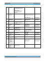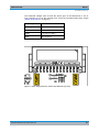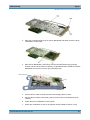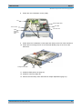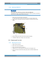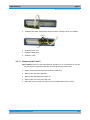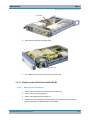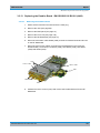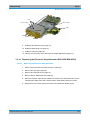
1
R&S®SGS100A SGMA RF Source Service Manual Service Manual Test and Measurement 1173.9111.02 – 06 This Service Manual provides servicing and maintenance procedures for the R&S® SGS100A © 2015 Rohde & Schwarz GmbH & Co. KG Muehldorfstr. 15, 81671 Munich, Germany Phone: +49 89 41 29 – 0 Fax: +49 89 41 29 12 164 E-mail: [email protected] Internet: http://www.rohde-schwarz.com Printed in Germany – Subject to change – Data without tolerance limits is not binding. R&S® is a registered trademark of Rohde & Schwarz GmbH & Co. KG. Trade names are trademarks of the owners. The following abbreviations are used throughout this manual: R&S®SGS100A is abbreviated as R&S SGS100A. Basic Safety Instructions Always read through and comply with the following safety instructions! All plants and locations of the Rohde & Schwarz group of companies make every effort to keep the safety standards of our products up to date and to offer our customers the highest possible degree of safety. Our products and the auxiliary equipment they require are designed, built and tested in accordance with the safety standards that apply in each case. Compliance with these standards is continuously monitored by our quality assurance system. The product described here has been designed, built and tested in accordance with the EC Certificate of Conformity and has left the manufacturer’s plant in a condition fully complying with safety standards. To maintain this condition and to ensure safe operation, you must observe all instructions and warnings provided in this manual. If you have any questions regarding these safety instructions, the Rohde & Schwarz group of companies will be happy to answer them. Furthermore, it is your responsibility to use the product in an appropriate manner. This product is designed for use solely in industrial and laboratory environments or, if expressly permitted, also in the field and must not be used in any way that may cause personal injury or property damage. You are responsible if the product is used for any purpose other than its designated purpose or in disregard of the manufacturer's instructions. The manufacturer shall assume no responsibility for such use of the product. The product is used for its designated purpose if it is used in accordance with its product documentation and within its performance limits (see data sheet, documentation, the following safety instructions). Using the product requires technical skills and, in some cases, a basic knowledge of English. It is therefore essential that only skilled and specialized staff or thoroughly trained personnel with the required skills be allowed to use the product. If personal safety gear is required for using Rohde & Schwarz products, this will be indicated at the appropriate place in the product documentation. Keep the basic safety instructions and the product documentation in a safe place and pass them on to the subsequent users. Observing the safety instructions will help prevent personal injury or damage of any kind caused by dangerous situations. Therefore, carefully read through and adhere to the following safety instructions before and when using the product. It is also absolutely essential to observe the additional safety instructions on personal safety, for example, that appear in relevant parts of the product documentation. In these safety instructions, the word "product" refers to all merchandise sold and distributed by the Rohde & Schwarz group of companies, including instruments, systems and all accessories. For product-specific information, see the data sheet and the product documentation. Safety labels on products The following safety labels are used on products to warn against risks and dangers. Symbol Meaning Notice, general danger location Symbol Meaning ON/OFF Power Observe product documentation Caution when handling heavy equipment Standby indication Danger of electric shock Direct current (DC) 1171.0000.42 - 08 Page 1 Basic Safety Instructions Symbol Meaning Symbol Meaning Caution ! Hot surface Alternating current (AC) Protective conductor terminal To identify any terminal which is intended for connection to an external conductor for protection against electric shock in case of a fault, or the terminal of a protective earth Direct/alternating current (DC/AC) Earth (Ground) Class II Equipment to identify equipment meeting the safety requirements specified for Class II equipment (device protected by double or reinforced insulation) Frame or chassis Ground terminal EU labeling for batteries and accumulators For additional information, see section "Waste disposal/Environmental protection", item 1. Be careful when handling electrostatic sensitive devices EU labeling for separate collection of electrical and electronic devices For additional information, see section "Waste disposal/Environmental protection", item 2. Warning! Laser radiation For additional information, see section "Operation", item 7. Signal words and their meaning The following signal words are used in the product documentation in order to warn the reader about risks and dangers. Indicates a hazardous situation which, if not avoided, will result in death or serious injury. Indicates a hazardous situation which, if not avoided, could result in death or serious injury. Indicates a hazardous situation which, if not avoided, could result in minor or moderate injury. Indicates information considered important, but not hazard-related, e.g. messages relating to property damage. In the product documentation, the word ATTENTION is used synonymously. These signal words are in accordance with the standard definition for civil applications in the European Economic Area. Definitions that deviate from the standard definition may also exist in other economic areas or military applications. It is therefore essential to make sure that the signal words described here are always used only in connection with the related product documentation and the related product. The use of signal words in connection with unrelated products or documentation can result in misinterpretation and in personal injury or material damage. 1171.0000.42 - 08 Page 2 Basic Safety Instructions Operating states and operating positions The product may be operated only under the operating conditions and in the positions specified by the manufacturer, without the product's ventilation being obstructed. If the manufacturer's specifications are not observed, this can result in electric shock, fire and/or serious personal injury or death. Applicable local or national safety regulations and rules for the prevention of accidents must be observed in all work performed. 1. Unless otherwise specified, the following requirements apply to Rohde & Schwarz products: predefined operating position is always with the housing floor facing down, IP protection 2X, use only indoors, max. operating altitude 2000 m above sea level, max. transport altitude 4500 m above sea level. A tolerance of ±10 % shall apply to the nominal voltage and ±5 % to the nominal frequency, overvoltage category 2, pollution degree 2. 2. Do not place the product on surfaces, vehicles, cabinets or tables that for reasons of weight or stability are unsuitable for this purpose. Always follow the manufacturer's installation instructions when installing the product and fastening it to objects or structures (e.g. walls and shelves). An installation that is not carried out as described in the product documentation could result in personal injury or even death. 3. Do not place the product on heat-generating devices such as radiators or fan heaters. The ambient temperature must not exceed the maximum temperature specified in the product documentation or in the data sheet. Product overheating can cause electric shock, fire and/or serious personal injury or even death. Electrical safety If the information on electrical safety is not observed either at all or to the extent necessary, electric shock, fire and/or serious personal injury or death may occur. 1. Prior to switching on the product, always ensure that the nominal voltage setting on the product matches the nominal voltage of the mains-supply network. If a different voltage is to be set, the power fuse of the product may have to be changed accordingly. 2. In the case of products of safety class I with movable power cord and connector, operation is permitted only on sockets with a protective conductor contact and protective conductor. 3. Intentionally breaking the protective conductor either in the feed line or in the product itself is not permitted. Doing so can result in the danger of an electric shock from the product. If extension cords or connector strips are implemented, they must be checked on a regular basis to ensure that they are safe to use. 4. If there is no power switch for disconnecting the product from the mains, or if the power switch is not suitable for this purpose, use the plug of the connecting cable to disconnect the product from the mains. In such cases, always ensure that the power plug is easily reachable and accessible at all times. For example, if the power plug is the disconnecting device, the length of the connecting cable must not exceed 3 m. Functional or electronic switches are not suitable for providing disconnection from the AC supply network. If products without power switches are integrated into racks or systems, the disconnecting device must be provided at the system level. 5. Never use the product if the power cable is damaged. Check the power cables on a regular basis to ensure that they are in proper operating condition. By taking appropriate safety measures and carefully laying the power cable, ensure that the cable cannot be damaged and that no one can be hurt by, for example, tripping over the cable or suffering an electric shock. 1171.0000.42 - 08 Page 3 Basic Safety Instructions 6. The product may be operated only from TN/TT supply networks fuse-protected with max. 16 A (higher fuse only after consulting with the Rohde & Schwarz group of companies). 7. Do not insert the plug into sockets that are dusty or dirty. Insert the plug firmly and all the way into the socket provided for this purpose. Otherwise, sparks that result in fire and/or injuries may occur. 8. Do not overload any sockets, extension cords or connector strips; doing so can cause fire or electric shocks. 9. For measurements in circuits with voltages Vrms > 30 V, suitable measures (e.g. appropriate measuring equipment, fuse protection, current limiting, electrical separation, insulation) should be taken to avoid any hazards. 10. Ensure that the connections with information technology equipment, e.g. PCs or other industrial computers, comply with the IEC 60950-1 / EN 60950-1 or IEC 61010-1 / EN 61010-1 standards that apply in each case. 11. Unless expressly permitted, never remove the cover or any part of the housing while the product is in operation. Doing so will expose circuits and components and can lead to injuries, fire or damage to the product. 12. If a product is to be permanently installed, the connection between the protective conductor terminal on site and the product's protective conductor must be made first before any other connection is made. The product may be installed and connected only by a licensed electrician. 13. For permanently installed equipment without built-in fuses, circuit breakers or similar protective devices, the supply circuit must be fuse-protected in such a way that anyone who has access to the product, as well as the product itself, is adequately protected from injury or damage. 14. Use suitable overvoltage protection to ensure that no overvoltage (such as that caused by a bolt of lightning) can reach the product. Otherwise, the person operating the product will be exposed to the danger of an electric shock. 15. Any object that is not designed to be placed in the openings of the housing must not be used for this purpose. Doing so can cause short circuits inside the product and/or electric shocks, fire or injuries. 16. Unless specified otherwise, products are not liquid-proof (see also section "Operating states and operating positions", item 1). Therefore, the equipment must be protected against penetration by liquids. If the necessary precautions are not taken, the user may suffer electric shock or the product itself may be damaged, which can also lead to personal injury. 17. Never use the product under conditions in which condensation has formed or can form in or on the product, e.g. if the product has been moved from a cold to a warm environment. Penetration by water increases the risk of electric shock. 18. Prior to cleaning the product, disconnect it completely from the power supply (e.g. AC supply network or battery). Use a soft, non-linting cloth to clean the product. Never use chemical cleaning agents such as alcohol, acetone or diluents for cellulose lacquers. Operation 1. Operating the products requires special training and intense concentration. Make sure that persons who use the products are physically, mentally and emotionally fit enough to do so; otherwise, injuries or material damage may occur. It is the responsibility of the employer/operator to select suitable personnel for operating the products. 1171.0000.42 - 08 Page 4 Basic Safety Instructions 2. Before you move or transport the product, read and observe the section titled "Transport". 3. As with all industrially manufactured goods, the use of substances that induce an allergic reaction (allergens) such as nickel cannot be generally excluded. If you develop an allergic reaction (such as a skin rash, frequent sneezing, red eyes or respiratory difficulties) when using a Rohde & Schwarz product, consult a physician immediately to determine the cause and to prevent health problems or stress. 4. Before you start processing the product mechanically and/or thermally, or before you take it apart, be sure to read and pay special attention to the section titled "Waste disposal/Environmental protection", item 1. 5. Depending on the function, certain products such as RF radio equipment can produce an elevated level of electromagnetic radiation. Considering that unborn babies require increased protection, pregnant women must be protected by appropriate measures. Persons with pacemakers may also be exposed to risks from electromagnetic radiation. The employer/operator must evaluate workplaces where there is a special risk of exposure to radiation and, if necessary, take measures to avert the potential danger. 6. Should a fire occur, the product may release hazardous substances (gases, fluids, etc.) that can cause health problems. Therefore, suitable measures must be taken, e.g. protective masks and protective clothing must be worn. 7. Laser products are given warning labels that are standardized according to their laser class. Lasers can cause biological harm due to the properties of their radiation and due to their extremely concentrated electromagnetic power. If a laser product (e.g. a CD/DVD drive) is integrated into a Rohde & Schwarz product, absolutely no other settings or functions may be used as described in the product documentation. The objective is to prevent personal injury (e.g. due to laser beams). 8. EMC classes (in line with EN 55011/CISPR 11, and analogously with EN 55022/CISPR 22, EN 55032/CISPR 32) Class A equipment: Equipment suitable for use in all environments except residential environments and environments that are directly connected to a low-voltage supply network that supplies residential buildings Note: Class A equipment is intended for use in an industrial environment. This equipment may cause radio disturbances in residential environments, due to possible conducted as well as radiated disturbances. In this case, the operator may be required to take appropriate measures to eliminate these disturbances. Class B equipment: Equipment suitable for use in residential environments and environments that are directly connected to a low-voltage supply network that supplies residential buildings Repair and service 1. The product may be opened only by authorized, specially trained personnel. Before any work is performed on the product or before the product is opened, it must be disconnected from the AC supply network. Otherwise, personnel will be exposed to the risk of an electric shock. 1171.0000.42 - 08 Page 5 Basic Safety Instructions 2. Adjustments, replacement of parts, maintenance and repair may be performed only by electrical experts authorized by Rohde & Schwarz. Only original parts may be used for replacing parts relevant to safety (e.g. power switches, power transformers, fuses). A safety test must always be performed after parts relevant to safety have been replaced (visual inspection, protective conductor test, insulation resistance measurement, leakage current measurement, functional test). This helps ensure the continued safety of the product. Batteries and rechargeable batteries/cells If the information regarding batteries and rechargeable batteries/cells is not observed either at all or to the extent necessary, product users may be exposed to the risk of explosions, fire and/or serious personal injury, and, in some cases, death. Batteries and rechargeable batteries with alkaline electrolytes (e.g. lithium cells) must be handled in accordance with the EN 62133 standard. 1. Cells must not be taken apart or crushed. 2. Cells or batteries must not be exposed to heat or fire. Storage in direct sunlight must be avoided. Keep cells and batteries clean and dry. Clean soiled connectors using a dry, clean cloth. 3. Cells or batteries must not be short-circuited. Cells or batteries must not be stored in a box or in a drawer where they can short-circuit each other, or where they can be short-circuited by other conductive materials. Cells and batteries must not be removed from their original packaging until they are ready to be used. 4. Cells and batteries must not be exposed to any mechanical shocks that are stronger than permitted. 5. If a cell develops a leak, the fluid must not be allowed to come into contact with the skin or eyes. If contact occurs, wash the affected area with plenty of water and seek medical aid. 6. Improperly replacing or charging cells or batteries that contain alkaline electrolytes (e.g. lithium cells) can cause explosions. Replace cells or batteries only with the matching Rohde & Schwarz type (see parts list) in order to ensure the safety of the product. 7. Cells and batteries must be recycled and kept separate from residual waste. Rechargeable batteries and normal batteries that contain lead, mercury or cadmium are hazardous waste. Observe the national regulations regarding waste disposal and recycling. Transport 1. The product may be very heavy. Therefore, the product must be handled with care. In some cases, the user may require a suitable means of lifting or moving the product (e.g. with a lift-truck) to avoid back or other physical injuries. 2. Handles on the products are designed exclusively to enable personnel to transport the product. It is therefore not permissible to use handles to fasten the product to or on transport equipment such as cranes, fork lifts, wagons, etc. The user is responsible for securely fastening the products to or on the means of transport or lifting. Observe the safety regulations of the manufacturer of the means of transport or lifting. Noncompliance can result in personal injury or material damage. 3. If you use the product in a vehicle, it is the sole responsibility of the driver to drive the vehicle safely and properly. The manufacturer assumes no responsibility for accidents or collisions. Never use the product in a moving vehicle if doing so could distract the driver of the vehicle. Adequately secure the product in the vehicle to prevent injuries or other damage in the event of an accident. 1171.0000.42 - 08 Page 6 Instrucciones de seguridad elementales Waste disposal/Environmental protection 1. Specially marked equipment has a battery or accumulator that must not be disposed of with unsorted municipal waste, but must be collected separately. It may only be disposed of at a suitable collection point or via a Rohde & Schwarz customer service center. 2. Waste electrical and electronic equipment must not be disposed of with unsorted municipal waste, but must be collected separately. Rohde & Schwarz GmbH & Co. KG has developed a disposal concept and takes full responsibility for take-back obligations and disposal obligations for manufacturers within the EU. Contact your Rohde & Schwarz customer service center for environmentally responsible disposal of the product. 3. If products or their components are mechanically and/or thermally processed in a manner that goes beyond their intended use, hazardous substances (heavy-metal dust such as lead, beryllium, nickel) may be released. For this reason, the product may only be disassembled by specially trained personnel. Improper disassembly may be hazardous to your health. National waste disposal regulations must be observed. 4. If handling the product releases hazardous substances or fuels that must be disposed of in a special way, e.g. coolants or engine oils that must be replenished regularly, the safety instructions of the manufacturer of the hazardous substances or fuels and the applicable regional waste disposal regulations must be observed. Also observe the relevant safety instructions in the product documentation. The improper disposal of hazardous substances or fuels can cause health problems and lead to environmental damage. For additional information about environmental protection, visit the Rohde & Schwarz website. Instrucciones de seguridad elementales ¡Es imprescindible leer y cumplir las siguientes instrucciones e informaciones de seguridad! El principio del grupo de empresas Rohde & Schwarz consiste en tener nuestros productos siempre al día con los estándares de seguridad y de ofrecer a nuestros clientes el máximo grado de seguridad. Nuestros productos y todos los equipos adicionales son siempre fabricados y examinados según las normas de seguridad vigentes. Nuestro sistema de garantía de calidad controla constantemente que sean cumplidas estas normas. El presente producto ha sido fabricado y examinado según el certificado de conformidad de la UE y ha salido de nuestra planta en estado impecable según los estándares técnicos de seguridad. Para poder preservar este estado y garantizar un funcionamiento libre de peligros, el usuario deberá atenerse a todas las indicaciones, informaciones de seguridad y notas de alerta. El grupo de empresas Rohde & Schwarz está siempre a su disposición en caso de que tengan preguntas referentes a estas informaciones de seguridad. Además queda en la responsabilidad del usuario utilizar el producto en la forma debida. Este producto está destinado exclusivamente al uso en la industria y el laboratorio o, si ha sido expresamente autorizado, para aplicaciones de campo y de ninguna manera deberá ser utilizado de modo que alguna persona/cosa pueda sufrir daño. El uso del producto fuera de sus fines definidos o sin tener en cuenta las instrucciones del fabricante queda en la responsabilidad del usuario. El fabricante no se hace en ninguna forma responsable de consecuencias a causa del mal uso del producto. 1171.0000.42 - 08 Page 7 Instrucciones de seguridad elementales Se parte del uso correcto del producto para los fines definidos si el producto es utilizado conforme a las indicaciones de la correspondiente documentación del producto y dentro del margen de rendimiento definido (ver hoja de datos, documentación, informaciones de seguridad que siguen). El uso del producto hace necesarios conocimientos técnicos y ciertos conocimientos del idioma inglés. Por eso se debe tener en cuenta que el producto solo pueda ser operado por personal especializado o personas instruidas en profundidad con las capacidades correspondientes. Si fuera necesaria indumentaria de seguridad para el uso de productos de Rohde & Schwarz, encontraría la información debida en la documentación del producto en el capítulo correspondiente. Guarde bien las informaciones de seguridad elementales, así como la documentación del producto, y entréguelas a usuarios posteriores. Tener en cuenta las informaciones de seguridad sirve para evitar en lo posible lesiones o daños por peligros de toda clase. Por eso es imprescindible leer detalladamente y comprender por completo las siguientes informaciones de seguridad antes de usar el producto, y respetarlas durante el uso del producto. Deberán tenerse en cuenta todas las demás informaciones de seguridad, como p. ej. las referentes a la protección de personas, que encontrarán en el capítulo correspondiente de la documentación del producto y que también son de obligado cumplimiento. En las presentes informaciones de seguridad se recogen todos los objetos que distribuye el grupo de empresas Rohde & Schwarz bajo la denominación de "producto", entre ellos también aparatos, instalaciones así como toda clase de accesorios. Los datos específicos del producto figuran en la hoja de datos y en la documentación del producto. Señalización de seguridad de los productos Las siguientes señales de seguridad se utilizan en los productos para advertir sobre riesgos y peligros. Símbolo Significado Aviso: punto de peligro general Observar la documentación del producto Símbolo Significado Tensión de alimentación de PUESTA EN MARCHA / PARADA Atención en el manejo de dispositivos de peso elevado Indicación de estado de espera (standby) Peligro de choque eléctrico Corriente continua (DC) Advertencia: superficie caliente Corriente alterna (AC) Conexión a conductor de protección Corriente continua / Corriente alterna (DC/AC) Conexión a tierra El aparato está protegido en su totalidad por un aislamiento doble (reforzado) Conexión a masa Distintivo de la UE para baterías y acumuladores Más información en la sección "Eliminación/protección del medio ambiente", punto 1. 1171.0000.42 - 08 Page 8 Instrucciones de seguridad elementales Símbolo Significado Símbolo Aviso: Cuidado en el manejo de dispositivos sensibles a la electrostática (ESD) Significado Distintivo de la UE para la eliminación por separado de dispositivos eléctricos y electrónicos Más información en la sección "Eliminación/protección del medio ambiente", punto 2. Advertencia: rayo láser Más información en la sección "Funcionamiento", punto 7. Palabras de señal y su significado En la documentación del producto se utilizan las siguientes palabras de señal con el fin de advertir contra riesgos y peligros. Indica una situación de peligro que, si no se evita, causa lesiones graves o incluso la muerte. Indica una situación de peligro que, si no se evita, puede causar lesiones graves o incluso la muerte. Indica una situación de peligro que, si no se evita, puede causar lesiones leves o moderadas. Indica información que se considera importante, pero no en relación con situaciones de peligro; p. ej., avisos sobre posibles daños materiales. En la documentación del producto se emplea de forma sinónima el término CUIDADO. Las palabras de señal corresponden a la definición habitual para aplicaciones civiles en el área económica europea. Pueden existir definiciones diferentes a esta definición en otras áreas económicas o en aplicaciones militares. Por eso se deberá tener en cuenta que las palabras de señal aquí descritas sean utilizadas siempre solamente en combinación con la correspondiente documentación del producto y solamente en combinación con el producto correspondiente. La utilización de las palabras de señal en combinación con productos o documentaciones que no les correspondan puede llevar a interpretaciones equivocadas y tener por consecuencia daños en personas u objetos. Estados operativos y posiciones de funcionamiento El producto solamente debe ser utilizado según lo indicado por el fabricante respecto a los estados operativos y posiciones de funcionamiento sin que se obstruya la ventilación. Si no se siguen las indicaciones del fabricante, pueden producirse choques eléctricos, incendios y/o lesiones graves con posible consecuencia de muerte. En todos los trabajos deberán ser tenidas en cuenta las normas nacionales y locales de seguridad del trabajo y de prevención de accidentes. 1171.0000.42 - 08 Page 9 Instrucciones de seguridad elementales 1. Si no se convino de otra manera, es para los productos Rohde & Schwarz válido lo que sigue: como posición de funcionamiento se define por principio la posición con el suelo de la caja para abajo, modo de protección IP 2X, uso solamente en estancias interiores, utilización hasta 2000 m sobre el nivel del mar, transporte hasta 4500 m sobre el nivel del mar. Se aplicará una tolerancia de ±10 % sobre el voltaje nominal y de ±5 % sobre la frecuencia nominal. Categoría de sobrecarga eléctrica 2, índice de suciedad 2. 2. No sitúe el producto encima de superficies, vehículos, estantes o mesas, que por sus características de peso o de estabilidad no sean aptos para él. Siga siempre las instrucciones de instalación del fabricante cuando instale y asegure el producto en objetos o estructuras (p. ej. paredes y estantes). Si se realiza la instalación de modo distinto al indicado en la documentación del producto, se pueden causar lesiones o, en determinadas circunstancias, incluso la muerte. 3. No ponga el producto sobre aparatos que generen calor (p. ej. radiadores o calefactores). La temperatura ambiente no debe superar la temperatura máxima especificada en la documentación del producto o en la hoja de datos. En caso de sobrecalentamiento del producto, pueden producirse choques eléctricos, incendios y/o lesiones graves con posible consecuencia de muerte. Seguridad eléctrica Si no se siguen (o se siguen de modo insuficiente) las indicaciones del fabricante en cuanto a seguridad eléctrica, pueden producirse choques eléctricos, incendios y/o lesiones graves con posible consecuencia de muerte. 1. Antes de la puesta en marcha del producto se deberá comprobar siempre que la tensión preseleccionada en el producto coincida con la de la red de alimentación eléctrica. Si es necesario modificar el ajuste de tensión, también se deberán cambiar en caso dado los fusibles correspondientes del producto. 2. Los productos de la clase de protección I con alimentación móvil y enchufe individual solamente podrán enchufarse a tomas de corriente con contacto de seguridad y con conductor de protección conectado. 3. Queda prohibida la interrupción intencionada del conductor de protección, tanto en la toma de corriente como en el mismo producto. La interrupción puede tener como consecuencia el riesgo de que el producto sea fuente de choques eléctricos. Si se utilizan cables alargadores o regletas de enchufe, deberá garantizarse la realización de un examen regular de los mismos en cuanto a su estado técnico de seguridad. 4. Si el producto no está equipado con un interruptor para desconectarlo de la red, o bien si el interruptor existente no resulta apropiado para la desconexión de la red, el enchufe del cable de conexión se deberá considerar como un dispositivo de desconexión. El dispositivo de desconexión se debe poder alcanzar fácilmente y debe estar siempre bien accesible. Si, p. ej., el enchufe de conexión a la red es el dispositivo de desconexión, la longitud del cable de conexión no debe superar 3 m). Los interruptores selectores o electrónicos no son aptos para el corte de la red eléctrica. Si se integran productos sin interruptor en bastidores o instalaciones, se deberá colocar el interruptor en el nivel de la instalación. 5. No utilice nunca el producto si está dañado el cable de conexión a red. Compruebe regularmente el correcto estado de los cables de conexión a red. Asegúrese, mediante las medidas de protección y de instalación adecuadas, de que el cable de conexión a red no pueda ser dañado o de que nadie pueda ser dañado por él, p. ej. al tropezar o por un choque eléctrico. 1171.0000.42 - 08 Page 10 Instrucciones de seguridad elementales 6. Solamente está permitido el funcionamiento en redes de alimentación TN/TT aseguradas con fusibles de 16 A como máximo (utilización de fusibles de mayor amperaje solo previa consulta con el grupo de empresas Rohde & Schwarz). 7. Nunca conecte el enchufe en tomas de corriente sucias o llenas de polvo. Introduzca el enchufe por completo y fuertemente en la toma de corriente. La no observación de estas medidas puede provocar chispas, fuego y/o lesiones. 8. No sobrecargue las tomas de corriente, los cables alargadores o las regletas de enchufe ya que esto podría causar fuego o choques eléctricos. 9. En las mediciones en circuitos de corriente con una tensión U eff > 30 V se deberán tomar las medidas apropiadas para impedir cualquier peligro (p. ej. medios de medición adecuados, seguros, limitación de tensión, corte protector, aislamiento etc.). 10. Para la conexión con dispositivos informáticos como un PC o un ordenador industrial, debe comprobarse que éstos cumplan los estándares IEC60950-1/EN60950-1 o IEC61010-1/EN 61010-1 válidos en cada caso. 11. A menos que esté permitido expresamente, no retire nunca la tapa ni componentes de la carcasa mientras el producto esté en servicio. Esto pone a descubierto los cables y componentes eléctricos y puede causar lesiones, fuego o daños en el producto. 12. Si un producto se instala en un lugar fijo, se deberá primero conectar el conductor de protección fijo con el conductor de protección del producto antes de hacer cualquier otra conexión. La instalación y la conexión deberán ser efectuadas por un electricista especializado. 13. En el caso de dispositivos fijos que no estén provistos de fusibles, interruptor automático ni otros mecanismos de seguridad similares, el circuito de alimentación debe estar protegido de modo que todas las personas que puedan acceder al producto, así como el producto mismo, estén a salvo de posibles daños. 14. Todo producto debe estar protegido contra sobretensión (debida p. ej. a una caída del rayo) mediante los correspondientes sistemas de protección. Si no, el personal que lo utilice quedará expuesto al peligro de choque eléctrico. 15. No debe introducirse en los orificios de la caja del aparato ningún objeto que no esté destinado a ello. Esto puede producir cortocircuitos en el producto y/o puede causar choques eléctricos, fuego o lesiones. 16. Salvo indicación contraria, los productos no están impermeabilizados (ver también el capítulo "Estados operativos y posiciones de funcionamiento", punto 1). Por eso es necesario tomar las medidas necesarias para evitar la entrada de líquidos. En caso contrario, existe peligro de choque eléctrico para el usuario o de daños en el producto, que también pueden redundar en peligro para las personas. 17. No utilice el producto en condiciones en las que pueda producirse o ya se hayan producido condensaciones sobre el producto o en el interior de éste, como p. ej. al desplazarlo de un lugar frío a otro caliente. La entrada de agua aumenta el riesgo de choque eléctrico. 18. Antes de la limpieza, desconecte por completo el producto de la alimentación de tensión (p. ej. red de alimentación o batería). Realice la limpieza de los aparatos con un paño suave, que no se deshilache. No utilice bajo ningún concepto productos de limpieza químicos como alcohol, acetona o diluyentes para lacas nitrocelulósicas. 1171.0000.42 - 08 Page 11 Instrucciones de seguridad elementales Funcionamiento 1. El uso del producto requiere instrucciones especiales y una alta concentración durante el manejo. Debe asegurarse que las personas que manejen el producto estén a la altura de los requerimientos necesarios en cuanto a aptitudes físicas, psíquicas y emocionales, ya que de otra manera no se pueden excluir lesiones o daños de objetos. El empresario u operador es responsable de seleccionar el personal usuario apto para el manejo del producto. 2. Antes de desplazar o transportar el producto, lea y tenga en cuenta el capítulo "Transporte". 3. Como con todo producto de fabricación industrial no puede quedar excluida en general la posibilidad de que se produzcan alergias provocadas por algunos materiales empleados ―los llamados alérgenos (p. ej. el níquel)―. Si durante el manejo de productos Rohde & Schwarz se producen reacciones alérgicas, como p. ej. irritaciones cutáneas, estornudos continuos, enrojecimiento de la conjuntiva o dificultades respiratorias, debe avisarse inmediatamente a un médico para investigar las causas y evitar cualquier molestia o daño a la salud. 4. Antes de la manipulación mecánica y/o térmica o el desmontaje del producto, debe tenerse en cuenta imprescindiblemente el capítulo "Eliminación/protección del medio ambiente", punto 1. 5. Ciertos productos, como p. ej. las instalaciones de radiocomunicación RF, pueden a causa de su función natural, emitir una radiación electromagnética aumentada. Deben tomarse todas las medidas necesarias para la protección de las mujeres embarazadas. También las personas con marcapasos pueden correr peligro a causa de la radiación electromagnética. El empresario/operador tiene la obligación de evaluar y señalizar las áreas de trabajo en las que exista un riesgo elevado de exposición a radiaciones. 6. Tenga en cuenta que en caso de incendio pueden desprenderse del producto sustancias tóxicas (gases, líquidos etc.) que pueden generar daños a la salud. Por eso, en caso de incendio deben usarse medidas adecuadas, como p. ej. máscaras antigás e indumentaria de protección. 7. Los productos con láser están provistos de indicaciones de advertencia normalizadas en función de la clase de láser del que se trate. Los rayos láser pueden provocar daños de tipo biológico a causa de las propiedades de su radiación y debido a su concentración extrema de potencia electromagnética. En caso de que un producto Rohde & Schwarz contenga un producto láser (p. ej. un lector de CD/DVD), no debe usarse ninguna otra configuración o función aparte de las descritas en la documentación del producto, a fin de evitar lesiones (p. ej. debidas a irradiación láser). 8. Clases de compatibilidad electromagnética (conforme a EN 55011 / CISPR 11; y en analogía con EN 55022 / CISPR 22, EN 55032 / CISPR 32) Aparato de clase A: Aparato adecuado para su uso en todos los entornos excepto en los residenciales y en aquellos conectados directamente a una red de distribución de baja tensión que suministra corriente a edificios residenciales. Nota: Los aparatos de clase A están destinados al uso en entornos industriales. Estos aparatos pueden causar perturbaciones radioeléctricas en entornos residenciales debido a posibles perturbaciones guiadas o radiadas. En este caso, se le podrá solicitar al operador que tome las medidas adecuadas para eliminar estas perturbaciones. Aparato de clase B: Aparato adecuado para su uso en entornos residenciales, así como en aquellos conectados directamente a una red de distribución de baja tensión que suministra corriente a edificios residenciales. 1171.0000.42 - 08 Page 12 Instrucciones de seguridad elementales Reparación y mantenimiento 1. El producto solamente debe ser abierto por personal especializado con autorización para ello. Antes de manipular el producto o abrirlo, es obligatorio desconectarlo de la tensión de alimentación, para evitar toda posibilidad de choque eléctrico. 2. El ajuste, el cambio de partes, el mantenimiento y la reparación deberán ser efectuadas solamente por electricistas autorizados por Rohde & Schwarz. Si se reponen partes con importancia para los aspectos de seguridad (p. ej. el enchufe, los transformadores o los fusibles), solamente podrán ser sustituidos por partes originales. Después de cada cambio de partes relevantes para la seguridad deberá realizarse un control de seguridad (control a primera vista, control del conductor de protección, medición de resistencia de aislamiento, medición de la corriente de fuga, control de funcionamiento). Con esto queda garantizada la seguridad del producto. Baterías y acumuladores o celdas Si no se siguen (o se siguen de modo insuficiente) las indicaciones en cuanto a las baterías y acumuladores o celdas, pueden producirse explosiones, incendios y/o lesiones graves con posible consecuencia de muerte. El manejo de baterías y acumuladores con electrolitos alcalinos (p. ej. celdas de litio) debe seguir el estándar EN 62133. 1. No deben desmontarse, abrirse ni triturarse las celdas. 2. Las celdas o baterías no deben someterse a calor ni fuego. Debe evitarse el almacenamiento a la luz directa del sol. Las celdas y baterías deben mantenerse limpias y secas. Limpiar las conexiones sucias con un paño seco y limpio. 3. Las celdas o baterías no deben cortocircuitarse. Es peligroso almacenar las celdas o baterías en estuches o cajones en cuyo interior puedan cortocircuitarse por contacto recíproco o por contacto con otros materiales conductores. No deben extraerse las celdas o baterías de sus embalajes originales hasta el momento en que vayan a utilizarse. 4. Las celdas o baterías no deben someterse a impactos mecánicos fuertes indebidos. 5. En caso de falta de estanqueidad de una celda, el líquido vertido no debe entrar en contacto con la piel ni los ojos. Si se produce contacto, lavar con agua abundante la zona afectada y avisar a un médico. 6. En caso de cambio o recarga inadecuados, las celdas o baterías que contienen electrolitos alcalinos (p. ej. las celdas de litio) pueden explotar. Para garantizar la seguridad del producto, las celdas o baterías solo deben ser sustituidas por el tipo Rohde & Schwarz correspondiente (ver lista de recambios). 7. Las baterías y celdas deben reciclarse y no deben tirarse a la basura doméstica. Las baterías o acumuladores que contienen plomo, mercurio o cadmio deben tratarse como residuos especiales. Respete en esta relación las normas nacionales de eliminación y reciclaje. Transporte 1. El producto puede tener un peso elevado. Por eso es necesario desplazarlo o transportarlo con precaución y, si es necesario, usando un sistema de elevación adecuado (p. ej. una carretilla elevadora), a fin de evitar lesiones en la espalda u otros daños personales. 1171.0000.42 - 08 Page 13 Instrucciones de seguridad elementales 2. Las asas instaladas en los productos sirven solamente de ayuda para el transporte del producto por personas. Por eso no está permitido utilizar las asas para la sujeción en o sobre medios de transporte como p. ej. grúas, carretillas elevadoras de horquilla, carros etc. Es responsabilidad suya fijar los productos de manera segura a los medios de transporte o elevación. Para evitar daños personales o daños en el producto, siga las instrucciones de seguridad del fabricante del medio de transporte o elevación utilizado. 3. Si se utiliza el producto dentro de un vehículo, recae de manera exclusiva en el conductor la responsabilidad de conducir el vehículo de manera segura y adecuada. El fabricante no asumirá ninguna responsabilidad por accidentes o colisiones. No utilice nunca el producto dentro de un vehículo en movimiento si esto pudiera distraer al conductor. Asegure el producto dentro del vehículo debidamente para evitar, en caso de un accidente, lesiones u otra clase de daños. Eliminación/protección del medio ambiente 1. Los dispositivos marcados contienen una batería o un acumulador que no se debe desechar con los residuos domésticos sin clasificar, sino que debe ser recogido por separado. La eliminación se debe efectuar exclusivamente a través de un punto de recogida apropiado o del servicio de atención al cliente de Rohde & Schwarz. 2. Los dispositivos eléctricos usados no se deben desechar con los residuos domésticos sin clasificar, sino que deben ser recogidos por separado. Rohde & Schwarz GmbH & Co.KG ha elaborado un concepto de eliminación de residuos y asume plenamente los deberes de recogida y eliminación para los fabricantes dentro de la UE. Para desechar el producto de manera respetuosa con el medio ambiente, diríjase a su servicio de atención al cliente de Rohde & Schwarz. 3. Si se trabaja de manera mecánica y/o térmica cualquier producto o componente más allá del funcionamiento previsto, pueden liberarse sustancias peligrosas (polvos con contenido de metales pesados como p. ej. plomo, berilio o níquel). Por eso el producto solo debe ser desmontado por personal especializado con formación adecuada. Un desmontaje inadecuado puede ocasionar daños para la salud. Se deben tener en cuenta las directivas nacionales referentes a la eliminación de residuos. 4. En caso de que durante el trato del producto se formen sustancias peligrosas o combustibles que deban tratarse como residuos especiales (p. ej. refrigerantes o aceites de motor con intervalos de cambio definidos), deben tenerse en cuenta las indicaciones de seguridad del fabricante de dichas sustancias y las normas regionales de eliminación de residuos. Tenga en cuenta también en caso necesario las indicaciones de seguridad especiales contenidas en la documentación del producto. La eliminación incorrecta de sustancias peligrosas o combustibles puede causar daños a la salud o daños al medio ambiente. Se puede encontrar más información sobre la protección del medio ambiente en la página web de Rohde & Schwarz. 1171.0000.42 - 08 Page 14 Instructions - Instrucciones Instructions for Electrostatic Discharge Protection Risk of damaging electronic components To avoid damage of electronic components, the operational site must be protected against electrostatic discharge (ESD). Wrist strap with cord Floor mat Heel strap Ground connection of operational site The following two methods of ESD protection may be used together or separately: , Wrist strap with cord to ground connection , Conductive floor mat and heel strap combination 1171.0300.62 E/Esp-3 Instructions - Instrucciones Instrucciones para la protección contra descargas electroestáticas Riesgo de avería de los componentes electrónicos Para evitar averías en los componentes electrónicos, el área de trabajo tiene que estar protegido contra descargas electroestáticas ESD (electrostatic discharge). Muñequera con cordón Estera Talonera Conexión a tierra del área de trabajo Los siguientes dos métodos de protección ESD pueden ser usados juntos o separados: , Muñequera con cordón para conexión a tierra , Combinación de estera antiestática y talonera 1171.0300.62 E/Esp-3 Procedure in Case of Service and Ordering of Spare Parts This section contains information on shipping an instrument to your service center and ordering spare parts. Please contact your local Rohde & Schwarz service center if you need service or repair work of your equipment or to order spare parts. You can find the current address of your representative on our . homepage Shipping the Instrument We require the following information in order to answer your inquiry fast and correctly and to determine whether the warranty is still valid for your instrument: ● ● ● ● ● ● ● Instrument model Serial number Firmware version Must the instrument be returned with this firmware? Detailed error description in case of repair Indication of desired calibration Contact person for possible questions In some countries, an RMA process is available for the return shipment of the instrument. For details, contact your local representative. When shipping the instrument, be careful to provide for sufficient mechanical and antistatic protection. ● ● Use the original packaging for transporting or shipping the instrument. The protective caps for the front and rear prevent damage to the operating elements and the connectors. If you do not use the original packaging, provide for sufficient padding to prevent the instrument from slipping inside the box. Wrap antistatic packing foil around the instrument to protect it from electrostatic charging. Rohde & Schwarz offers repair and calibrations of the test systems it produces. The calibration documentation fulfills ISO 17025 requirements. Shipping Defective Modules Also when shipping a module, be careful to provide for sufficient mechanical and antistatic protection. ● ● Ship the module in a sturdy, padded box. Wrap the module in antistatic foil. If the packaging is only antistatic but not conductive, additional conductive packaging is required. The additional packaging is not required if the tightly fitting packaging is conductive. Exception: If the module contains a battery, the tightly fitting packaging must always consist of antistatic, nonchargeable material to protect the battery from being discharged. 1171.0200.61-02 1 Ordering Spare Parts To deliver spare parts promptly and correctly, we need the following information: ● ● ● ● ● ● ● ● Stock number (see list of spare parts in chapter "Documents") Designation Component number according to list of spare parts Number of pieces Instrument type for which the spare part is needed Instrument stock number Instrument serial number Contact person for possible questions Refurbished Modules Refurbished modules are an economical alternative to original modules. Bear in mind that refurbished modules are not new, but repaired and fully tested parts. They may have traces from use, but they are electrically and mechanically equivalent to new modules. Your Rohde & Schwarz representative will be happy to inform you about which modules are available as refurbished modules. Taking Back Defective Replaced Modules Defective modules of the replacement program which cannot be repaired are taken back within three months following delivery. A repurchasing value is credited. Excluded are parts which cannot be repaired, e.g. printed boards that are burnt, broken or damaged by attempts to repair them, incomplete modules, and parts with severe mechanical damage. Please return the defective replacement modules, together with the accompanying document for returned merchandise, which you received with the spare module. We need the following information: ● ● ● ● ● ● ● Stock number, serial number and designation of the removed part Detailed error description Stock number, serial number and type of instrument from which the module was removed Date of removal Name of the engineer/technician who replaced the module R&S ordering number Service reference number (if available) 1171.0200.61-02 2 R&S SGS100A Table of Contents Table of Contents 1 Performance Test ......................................................................................... 8 1.1 Test Equipment ......................................................................................................................8 1.2 Test Assemblies ...................................................................................................................10 1.2.1 Test Assembly for Output Impedance (VSWR) ......................................................................10 1.2.2 Test Assembly for Setting Time .............................................................................................. 11 1.2.3 Test Assembly for I/Q Modulation .......................................................................................... 11 1.2.4 Test Assembly for Pulse modulation ...................................................................................... 11 1.3 Preparation, Recommended Test Frequencies and Levels .............................................12 1.4 Test Procedures ...................................................................................................................13 1.4.1 Reference Frequency.............................................................................................................13 1.4.1.1 Internal Reference Mode........................................................................................................13 1.4.1.2 External Reference mode ......................................................................................................14 1.4.2 Frequency ..............................................................................................................................15 1.4.2.1 Frequency Setting ..................................................................................................................15 1.4.2.2 Setting Time ...........................................................................................................................15 1.4.3 Spectral Purity ........................................................................................................................19 1.4.3.1 Harmonics ..............................................................................................................................19 1.4.3.2 Subharmonics ........................................................................................................................20 1.4.3.3 Nonharmonics ........................................................................................................................20 1.4.3.4 Non-systematic nonharmonics ...............................................................................................22 1.4.3.5 Wideband Noise .....................................................................................................................23 1.4.3.6 SSB Phase Noise ...................................................................................................................25 1.4.3.7 Residual FM ...........................................................................................................................26 1.4.3.8 Residual AM ...........................................................................................................................28 1.4.4 Level Data ..............................................................................................................................30 1.4.4.1 Level Uncertainty ...................................................................................................................30 1.4.4.2 Output Impedance ..................................................................................................................32 1.4.4.3 Setting Time ...........................................................................................................................33 1.4.5 Pulse Modulation (Option R&S SGS-K22) .............................................................................35 1.4.5.1 ON/OFF Ratio ........................................................................................................................35 1.4.5.2 Rise/ Fall Time and Pulse Overshoot .....................................................................................36 Service Manual 1173.9111.02 -06 3 R&S SGS100A Table of Contents 1.4.5.3 Video Crosstalk ......................................................................................................................37 1.4.5.4 Pulse Video Signal .................................................................................................................38 1.4.6 I/Q modulation ........................................................................................................................39 1.4.6.1 Input Impedance (VSWR) ......................................................................................................39 1.4.6.2 Error Vector ............................................................................................................................40 1.4.6.3 Residual Carrier and Leakage ...............................................................................................41 1.4.6.4 I/Q Imbalance .........................................................................................................................42 1.4.6.5 Adjacent Channel Power for 3GPP FDD ...............................................................................43 1.4.6.6 Frequency Response of Baseband Bypass path ...................................................................44 1.4.6.7 Level linearity of Baseband Bypass path ...............................................................................45 1.4.7 Phase Coherence Levels (Option R&S SGS-K90) ................................................................46 1.4.8 PCI Express Interface ............................................................................................................46 2 Adjustment ................................................................................................. 47 2.1 Procedures after Module Replacement .............................................................................47 2.1.1 Restore Ethernet MAC Adress ...............................................................................................48 2.2 Adding Hardware Options ...................................................................................................48 2.3 Internal Adjustments ............................................................................................................50 2.4 External Adjustments Requiring Measurement Equipment ............................................50 2.5 Adjustment of internal Reference Frequency ...................................................................50 2.5.1 Adjustment .............................................................................................................................51 2.6 Internal Self Test ..................................................................................................................51 3 Repair .......................................................................................................... 52 3.1 Functional Description ........................................................................................................53 3.1.1 Power Supply Module ............................................................................................................53 3.1.2 Controller Board .....................................................................................................................53 3.1.2.1 Switching regulators ...............................................................................................................53 3.1.2.2 Controller ................................................................................................................................53 3.1.2.3 FPGA (SIGMA_COM) ............................................................................................................53 3.1.2.4 Diagnostic Multiplexer ............................................................................................................53 3.1.2.5 EEPROM ................................................................................................................................53 3.1.2.6 Temperature sensor ...............................................................................................................54 3.1.3 RF Mainboard ........................................................................................................................54 3.1.3.1 Block diagram ........................................................................................................................54 Service Manual 1173.9111.02 -06 4 R&S SGS100A Table of Contents 3.1.3.2 Implemented functions ...........................................................................................................55 3.1.3.3 Internal and external reference ..............................................................................................55 3.1.3.4 Main 1000 MHz oscillator .......................................................................................................55 3.1.3.5 RF Synthesizer/ DDS module ................................................................................................55 3.1.3.6 Vector modulator ....................................................................................................................56 3.1.3.7 Harmonics filters ....................................................................................................................56 3.1.3.8 Automatic Level control ..........................................................................................................56 3.1.3.9 Fan Controller ........................................................................................................................56 3.1.3.10 Supply voltage control and filtering ........................................................................................56 3.1.4 Doubler Board ........................................................................................................................57 3.1.4.1 Doubler Board architecture ....................................................................................................57 3.1.4.2 Doubler Board diagram ..........................................................................................................57 3.1.5 Step Attenuator .......................................................................................................................58 3.1.5.1 Step Attenuator architecture ...................................................................................................58 3.1.5.2 Step Attenuator diagram ........................................................................................................58 3.1.5.3 Power Amplifiers ....................................................................................................................58 3.1.5.4 Voltage Regulators and filtering .............................................................................................58 3.1.6 R&S SGS-B1 Reference Oscillator ........................................................................................59 3.2 Troubleshooting ...................................................................................................................60 3.2.1 Measuring Equipment and Accessories .................................................................................61 3.2.2 Switch-On Problems ..............................................................................................................61 3.2.2.1 Test Points on Controller Board .............................................................................................63 3.2.3 Keyboard and LED Test .........................................................................................................64 3.2.4 USB Cable Test ......................................................................................................................65 3.2.5 Troubleshooting with Internal Selftest ....................................................................................66 3.2.6 Troubleshooting with Internal Adjustments ............................................................................67 3.2.7 Instrument Faults ...................................................................................................................68 3.2.7.1 Fuses .....................................................................................................................................74 3.2.8 Troubleshooting − RF Mainboard ..........................................................................................76 3.2.8.1 Internal Adjustment “Adjust All” ..............................................................................................76 3.2.8.2 Supply Voltages .....................................................................................................................77 3.2.8.3 Input and Output Signals........................................................................................................78 3.2.8.4 Error Messages Concerning the RF Mainboard ....................................................................80 Service Manual 1173.9111.02 -06 5 R&S SGS100A Table of Contents 3.2.8.5 Warnings Concerning the RF Mainboard ...............................................................................80 3.2.8.6 Frequency Error .....................................................................................................................81 3.2.9 Troubleshooting − Reference Oscillator option R&S SGS-B1 ...............................................81 3.2.9.1 Input and Output Signals........................................................................................................81 3.2.9.2 Error Messages Concerning the Reference Oscillator Module..............................................83 3.2.9.3 Frequency Error, Reference Oscillator Adjustment ................................................................84 3.2.10 Troubleshooting − Active Step Attenuator ..............................................................................84 3.2.10.1 Supply Voltages .....................................................................................................................84 3.2.11 Troubleshooting − Doubler Board option R&S SGS-B112/-B112V ........................................86 3.2.11.1 Supply Voltages .....................................................................................................................86 3.2.11.2 Input and Output Signals........................................................................................................87 3.3 Module Replacement and Upgrade ....................................................................................88 3.3.1 Required Tools .......................................................................................................................88 3.3.2 Module Overview ...................................................................................................................88 3.3.3 After Replacing an Assembly .................................................................................................89 3.3.4 Removing the Case................................................................................................................89 3.3.5 Installing the Case ..................................................................................................................90 3.3.6 Replacing the EMC Panel ......................................................................................................91 3.3.6.1 Removing the EMC Panel ......................................................................................................91 3.3.6.2 Installing the EMC Panel ........................................................................................................91 3.3.7 Replacing the Power Supply (A50) ........................................................................................92 3.3.7.1 Removing the Power Supply ..................................................................................................92 3.3.7.2 Installing the Power Supply (A50) ..........................................................................................94 3.3.8 Replacing the RF Mainboard (A200) or Controller Board (A100) ..........................................95 3.3.8.1 Removing the RF Mainboard or Controller Board .................................................................95 3.3.8.2 Installing the RF Mainboard (A200) or Controller Board (A100) ............................................97 3.3.8.3 Replacing the SIM Card .......................................................................................................100 3.3.9 Replacing the Front Unit ......................................................................................................100 3.3.9.1 Removing the Front Unit ......................................................................................................100 3.3.10 Replacing the Flex Switch Board A300 ................................................................................101 3.3.10.1 Removing the Flex Switch Board and Push-Button Board ..................................................101 3.3.10.2 Installing the Flex Switch Board and the Push-Button Board ..............................................102 3.3.11 Replacing the Fan E1 ...........................................................................................................103 Service Manual 1173.9111.02 -06 6 R&S SGS100A Table of Contents 3.3.12 Replacing the OCXO Board R&S SGS-B1 ..........................................................................104 3.3.12.1 Removing the OCXO Board .................................................................................................104 3.3.12.2 Installing the OCXO Board ...................................................................................................105 3.3.13 Replacing the Doubler Board - R&S SGS-B112/-B112V (A400) .........................................106 3.3.13.1 Removing the Doubler Board ...............................................................................................106 3.3.13.2 Installing the Doubler Board .................................................................................................107 3.3.14 Replacing the Electronic Step Attenuator R&S SGS-B26 (A500) ........................................108 3.3.14.1 Removing the Electronic Step Attenuator ............................................................................108 3.3.14.2 Installing the Electronic Step Attenuator .............................................................................. 110 4 Firmware Update ....................................................................................... 112 5 Factory Recover and USB Install ............................................................. 113 6 Documents ................................................................................................. 114 6.1 Spare Parts.......................................................................................................................... 114 6.1.1 Available Power Cables ....................................................................................................... 114 6.2 Spare Part List and Mechanical Drawings ....................................................................... 115 Index ............................................................................................................ 116 Service Manual 1173.9111.02 -06 7 R&S SGS100A Performance Test Test Equipment 1 Performance Test Test Instructions To ensure that rated specifications are maintained, the following preparations must be made prior to checking the rated characteristics: ● ● ● ● Check the instrument condition. Make sure the instrument fan operation is not constrained by dust etc. The fan can be inspected through the air intake at the case bottom side. Allow for a minimum warm-up time of 30 minutes at ambient temperature. Carry out all internal adjustments. The values are specified in the data sheet. Additional uncertainties introduced by the measurement equipment must be taken into account when checking the rated values. This performance test describes the steps for testing the R&S SGS100A Signal Generator family and the installed options with respect to function and compliance with specifications. In the following, the term DUT (Device Under Test) is used for any signal generator of this family. The tests to be performed depend on the installed options. The values are given in the data sheet of the respective instrument 1.1 Test Equipment Table 1-1 Measuring equipment and accessories Item Type of equipment Recommended characteristics or features 1 Frequency counter 1 Hz to RFmax, resolution 0.1 Hz (included in RF analyzer item 19) 2 Reference source for SSB noise measurements Identical generator as DUT or generator with at least 10 dB lower SSB noise as DUT Frequency range up to RFmax Service Manual 1173.9111.02 -06 Recommended model R&S Order No. R&S SGS100A with adequate frequency option or 1416.0505.02 R&S SMF100A only for f ≥ 1000 MHz or 1158.2878 1167.0000.02 R&S SMA100A with option R&S SMA-B106 and option R&S SMA-B22 only for f 6000 MHz 1400.0000K02 1405.0809.02 1405.1805.02 8 R&S SGS100A Performance Test Test Equipment 4 Controller Industry standard PC/XT/AT with IEC-60625 interface and USB interface and LAN interface and optional PCI Express interface 5 Signal generator 1 MHz to RFmax R&S SMB100A with adequate frequency option or 1406.6000K03 R&S SMF100A with option R&S SMF-B2 1167.0000K02 1167.4005.02 6 Phase noise test assembly Phase Noise Test Set R&S FSUP 26 or R&S FSUP 50 1166.3505.27 1166.3505.51 7 Oscilloscope Bandwidth ≥ 500 MHz, two channels with DC coupling R&S RTM1052 or similar 1305.0008.52 8 RF power meter 1 MHz to RFmax R&S NRP with R&S NRP-Z55 or R&S NRP-Z51 1143.8500.02 1138.2008.02 1138.0005.0x 9 Mixer 10 MHz to RFmax IF down to DC 10 VSWR bridge 1 MHz to RFmax directivity > 30 dB f < 4 GHz: R&S ZRC 3 GHz f < 12.75 GHz: Agilent 773D 1039.9492.55 14 Arbitrary wave generator two channels R&S SMBV R&S SMU 1407.6004K02 1141.2005.02 15 AC/DC voltmeter 10 Hz to 10 MHz R&S URE3 350.5315.03 16 Broadband FM demodulator included in RF analyzer item 19 19 RF analyzer & Demodulator for analog modulations & FMdemodulator 1 MHz to RFmax * 2 R&S FSQ26 with options R&S FSU-B25 R&S FSQ K7 1155.5001.26 1044.9298.02 1141.1796.02 20 Software for simulation of digital modulations Generation of data for ARB generator R&S WinIQSIM Service Manual 1173.9111.02 -06 9 R&S SGS100A Performance Test Test Assemblies 21 Lowpass filter (2 pieces required) Lowpass filter 2.5 MHz to remove WCDMA I/Q BB test signal noise Passband loss < 0.5 dB for f = 0…2 MHz Stopband loss > 15 dB for f > 3 MHz Linearity IP3 > 50 dBm 23 PCIe cable PCIe extension cable with single lane connectors, length max. 5 m One Stop Systems OSS-PCIe-CBL-x1 or equivalent 24 PCIe device External single lane PCIe device R&S PCIe test port 5009.9002.02 1.2 Test Assemblies 1.2.1 Test Assembly for Output Impedance (VSWR) Test equipment - VSWR bridge (item 10) Signal generator (item 5) RF analyzer (item 19) Test setup 2nd RF 6 dB OUTPUT COUPLED INPUT 10 MHz Ref. Note: Service Manual 1173.9111.02 -06 The INPUT of the directional coupler is directly screwed to the DUT. The second signal generator is connected to the line connector (OUTPUT), the analyzer to the coupling output (COUPLED) of the directional coupler. 10 R&S SGS100A Performance Test Test Assemblies 1.2.2 Test Assembly for Setting Time Test equipment - RF analyzer (item 19) Test setup Controller LAN Trigger pulse 10 MHz Ref. RF 1.2.3 Test Assembly for I/Q Modulation Test equipment - RF analyzer (item 19) Arbitrary waveform generator (item 14) Software for simulation of digital modulations (item 20) Controller (item 4) Test setup Processor IEEE(IEC) Bus I Q DUT Ref. 10 MHz ModulationsARB analysator generator RF analyzer (dig. demodulation) RF 1.2.4 Test Assembly for Pulse modulation Test equipment - Oscilloscope ( item 7), Signal Generator (item 5) Mixer (item 9) Test setup Pulse 10 MHz Ref. LO Trig Service Manual 1173.9111.02 -06 RF RF 11 R&S SGS100A Performance Test Preparation, Recommended Test Frequencies and Levels 1.3 Preparation, Recommended Test Frequencies and Levels To ensure proper conditions for the performance test and prevent setting errors, the instrument must be prepared as follows: Check the instrument condition. Make sure the instrument fan operation is not constrained by dust etc. The fan can be inspected through the air intake at the case bottom side. Allow for a minimum warm-up time of 30 minutes at ambient temperature. Carry out all internal adjustments (see operating manual, chapter 4, section "Internal Adjustment - Setup-System"). Perform Preset to establish a defined initial state before configuring a new measurement. The following sections describe the procedures for checking the rated values. The values are specified in the data sheet. Additional uncertainties introduced by the measurement equipment must be taken into account when checking the rated values. The following table lists the important internal switch point frequencies and the recommended measurement frequencies derived from these frequencies. We recommend measurements at these frequencies unless particular test frequencies are specified. In the following, RFmax is the maximal settable RF (depending on installed options). Table 1-2 Range limits, main test frequencies for CW Mode Range Frequency Hardware switching points Recommended test frequencies Direct DDS Synthesis 1 MHz f 80 MHz 80 MHz Divider /64 80 MHz < f 93.75 MHz 93.75 MHz 1 MHz; 5.001 MHz; 10.01 MHz; 20.01 MHz, 40.01 MHz, 60.01 MHz, 80 MHz 80.01 MHz; 93.75 MHz Divider /32 93.75 MHz < f 187.5 MHz 120 MHz; 187.5 MHz 93.76 MHz; 120 MHz; 187.5 MHz Divider /16 187.5 MHz < f 375 MHz 265 MHz; 375MHz 187.6 MHz; 265 MHz; 375 MHz Divider /8 375 MHz < f 750 MHz 530MHz; 750MHz 375.1 MHz; 530 MHz; 750 MHz Divider /4 750 MHz < f 1500 MHz 1060MHz; 1500 MHz 750.1 MHz; 1060 MHz; 1500 MHz Divider /2 1500 MHz < f 3 GHz 2120 MHz; 3000 MHz 1501 MHz; 2120 MHz; 3000 MHz Base octave 3 GHz < f 6.5 GHz 4000 MHz, 6000 MHz, 6500 MHz Doubler range 6.5 GHz < f 12.75 GHz 7200 MHz, 7300 MHz, 8900 MHz, 9400 MHz, 10700 MHz 3001 MHz; 3500 MHz; 4000 MHz; 5100 MHz; 6000 MHz; 6001 MHz; 6500 MHz 6501 MHz; 7200 MHz; 7201 MHz; 7300 MHz; 7301 MHz; 8100 MHz; 8900 MHz; 8901 MHz; 9400 MHz; 9401 MHz; 9800 MHz; 10700 MHz; 10701 MHz; 11700 MHz; 12750 MHz RFmax is the maximum output frequency of the instrument according to its frequency option (6 GHz or 12.75 GHz). For high-resolution measurements in the entire frequency range, a logarithmic frequency grid in 1-2-5 sequence is recommended up to 50 MHz; above this value, linear 50 MHz steps should be used up to the upper limit frequency. Service Manual 1173.9111.02 -06 12 R&S SGS100A Performance Test Test Procedures The recommended test levels are at the upper and lower switching threshold of the attenuator. The electronic attenuator of the DUT is switched depending on frequency, modulation parameters and level according to an internal stored table in approximately 6 dB steps. The switching thresholds can be detected under Attenuator fixed range in the Level menu. After setting all other parameters, the threshold level can be detected by level variation. The level at which the attenuator fixed range changes is the threshold. By measuring at the last level setting of one range and the first level setting of the next range, the internal setting range borders are used. In the following, Pmax is the highest level before switching the attenuator, and Pmin is defined as Pmax – 7 dB for the electronic step attenuator R&S SGS-B26. 1.4 Test Procedures 1.4.1 Reference Frequency 1.4.1.1 Internal Reference Mode Important: Allow the DUT to warm up for at least 2 hours before starting the measurement. Test equipment - RF power meter, (item 8) Frequency counter (item 1) Test setup Connect an RF power meter to the REF OUT output (on rear panel). Measurement Measure the output level. It should be within the data sheet specifications. DUT setting: Internal Reference, Ref Output Frequency set to 10 MHz / 1000 MHz Test setup Connect a calibrated frequency counter to the REF OUT output (on rear panel). Measurement Measure the frequency. DUT setting: Internal Reference, Reference output set to 10 MHz / 1000 MHz The frequency deviation must not exceed the sum of deviations resulting from the frequency error in the rated temperature range and from aging. Service Manual 1173.9111.02 -06 13 R&S SGS100A Performance Test Test Procedures 1.4.1.2 External Reference mode Test equipment Frequency counter (item 1) Signal generator (item 5) RF power meter (item 8) - Test method The external reference input frequency of the DUT is varied according to the data sheet and the RF output signal frequency is controlled with a frequency counter to follow this variation. The Reference output level is tested. Preparation of measurement Connect the signal generator RF output to the REF IN input for the external reference (on rear panel) of the DUT. Connect a calibrated frequency counter to the RF output. Synchronize the signal generator and the frequency counter. Setting on DUT: - RF on - Level: 0 dBm (suitable level for the frequency counter) - Frequency: 1 GHz - Setup Reference Oscillator Source: External Ext Ref Frequency: 10 MHz REF/LO Output: REF Output Frequency: 10 MHz Setting on signal generator: - RF on - Level: 0 dBm Measurement Set the generator frequency to the nominal Ext Ref frequency +/10 ppm. Measure the output frequency of the DUT. There must be no relative frequency error and no error message in the display of the DUT. Connect the frequency counter to the DUT Ref Out connector. Measure the Ref Out frequency. There must be no relative frequency error compared to the Ext Ref frequency delivered to the DUT. Connect a RF power meter to the DUT Ref Out connector. The Ref Out level shall be within the data sheet specifications. Repeat the measurement for following combinations: Ext Ref Frequency Ext Ref Level Ref Output Frequency Ref Out Level Limit 10 MHz 0 dBm 10 MHz see data sheet 10 MHz 0 dBm 1000 MHz see data sheet 100 MHz 0 dBm 100 MHz see data sheet 100 MHz 0 dBm 1000 MHz see data sheet 1000 MHz 0 dBm 1000 MHz see data sheet Service Manual 1173.9111.02 -06 14 R&S SGS100A Performance Test Test Procedures 1.4.2 Frequency 1.4.2.1 Frequency Setting Test method The frequency setting is tested by running the internal synthesizer adjustments to check the frequency overlap of the VCOs Measurement Run: Setup Internal Adjustments Adjust Synthesis There must be no error message. 1.4.2.2 Setting Time Test assembly See section "Test Assembly for Setting Time", page 11. Test method The spectrum analyzer operates as an FM demodulator. A controller transmits the start and the stop frequency via the LAN interface by a special remote command. The DUT trigger connector on the rear panel is programmed as trigger pulse output. The analyzer is triggered by the signal generated on the DUT trigger output. At switch over from start to stop frequency, the settling procedure is displayed on the screen of the analyzer. Synchronize the reference frequencies of the DUT and the analyzer. Make LAN and RF connections. Connect spectrum analyzers trigger connector to DUT trigger output Settings on DUT: - :CONNector:TRIGger:OMODe MLATency - Frequency: start frequency unmodulated, - Level Settings/Setting Characteristic: Auto, - Level: 0 dBm, Settings on spectrum analyzer: - AMPT/REF LEVEL 0 dBm - FREQ/CENTER/STOP FREQUENCY - FM DEMOD ON - DEMOD BW 100 kHz - RANGE /DEVIATION PER DIV 200 Hz - MEAS TIME 2 ms - TRIGGER EXTERN - External triggering by positive edge at 1.4 V. Preparation of measurement Service Manual 1173.9111.02 -06 15 R&S SGS100A Performance Test Test Procedures Measurement Service Manual 1173.9111.02 -06 Settings on analyzer: - Set the analyzer to the stop frequency Set the DUT to the start frequency fstart Send the stop frequency fstop from the controller to the DUT by using the command :TEST:SPEED Stop frequency, Test level The externally triggered analyzer displays the settling curve. The setting time is defined as the time required to make the frequency deviation from the stop frequency less than the specified deviation in the data sheet. Switch on IQ-Modulation: I/Q Settings menu: Source Analog Wideband I/Q Input State On and supply 0.5 V DC to the Iext Input Repeat the measurement 16 R&S SGS100A Performance Test Test Procedures Recommended test frequencies and modes Service Manual 1173.9111.02 -06 fstart fstop Mode 79.9 MHz 6000 MHz CW 6000 MHz 79.9 MHz CW 93.7 MHz 93.8 MHz CW, IQ 93.8 MHz 93.7 MHz 187.4 MHz 187.6 MHz 187.6 MHz 187.4 MHz 374.9 MHz 375.1 MHz 375.1 MHz 374.9 MHz 749.9 MHz 750.1 MHz 750.1 MHz 749.9 MHz 1499.9 MHz 1500.1 MHz 1500.1 MHz 1499.9 MHz 2999.9 MHz 3000.1 MHz 3000.1 MHz 2999.9 MHz 3000.1 MHz 6000 MHz 6000 MHz 3000.1 MHz 79.9 MHz 6000.1 MHz 6000.1 MHz 79.9 MHz 79.9 MHz 12750 MHz 12750 MHz 79.9 MHz 5999.9 MHz 12750 MHz 12750 MHz 5999.9 MHz 6000.1 MHz 12750 MHz 12750 MHz 6000.1 MHz CW, IQ CW, IQ CW, IQ CW, IQ CW, IQ CW, IQ CW, IQ CW, IQ CW, IQ CW, IQ CW, IQ CW, IQ CW, IQ CW CW CW CW CW, IQ CW, IQ CW, IQ CW, IQ 17 R&S SGS100A Performance Test Test Procedures Example of Measurement: IFB 1 MHz AQT 1 ms Marker 1 [T1 ] 94.964309692 Hz Ref 0 Hz Att 30 dB 334.935897 µs * 500 A 400 SGL 1 SA CLRWR TRG 300 200 1 100 0 -100 -200 -300 -400 -500 Center 750.1 MHz Date: 12.MAR.2012 100 µs/ 16:08:54 The marker is set to the time when the trace enters the specified interval of 750.1 MHz ± 150 Hz. The setting time is 335 µs. Service Manual 1173.9111.02 -06 18 R&S SGS100A Performance Test Test Procedures 1.4.3 Spectral Purity 1.4.3.1 Harmonics Test equipment RF analyzer (item 19) Test setup Connect the RF analyzer to the RF output of the DUT. Synchronize the reference frequencies of analyzer and DUT. Measurement Settings on analyzer: Reference level = 20 dBm, 10 dB/div. Span 0 Hz, Resolution bandwidth 10 kHz Settings on DUT: - Frequency: test frequencies, unmodulated - Level: test levels First measure the level of the fundamental Pf at the test frequency f as a reference. Then measure the signal levels P2*f and P3*f at twice and three times the carrier frequency f. The harmonic spacing is the measured harmonic level referred to the fundamental: HD2 = Pf - P2*f HD3 = Pf – P3*f (in dBc = referred to the carrier) Recommended test frequencies and levels Test frequencies: 1 MHz; 5.001 MHz; 10.01 MHz; 20.01 MHz; 40.01 MHz; 60.01 MHz; 80 MHz; 80.01 MHz; 93.75 MHz; 93.76 MHz; 120 MHz; 187.5 MHz; 187.6 MHz; 265 MHz; 375 MHz; 375.1 MHz; 530 MHz; 750 MHz; 750.1 MHz; 1060 MHz; 1500 MHz; 1501 MHz; 2120 MHz; 3000 MHz; 3001 MHz; 3500 MHz; 4000 MHz; 5100 MHz; 6 GHz; 6001 MHz; 6500 MHz; 6501 MHz; 7200 MHz; 7201 MHz; 7300 MHz; 7301 MHz; 8100 MHz; 8900 MHz; 8901 MHz; 9400 MHz; 9401 MHz; 9800 MHz; 10700 MHz; 10701 MHz; 11700 MHz; 12750 MHz Test level: +8 dBm Repeat the measurement with IQ-Modulation switched on: I/Q Settings menu: State On I/Q Wideband Off and supply 0.5 V DC to the Iext Input Test frequencies: 80 MHz; 80.01 MHz; 93.75 MHz; 93.76 MHz; 120 MHz; 187.5 MHz; 187.6 MHz; 265 MHz; 375 MHz; 375.1 MHz; 530 MHz; 750 MHz; 750.1 MHz; 1060 MHz; 1500 MHz; 1501 MHz; 2120 MHz; 3000 MHz; 3001 MHz; 3500 MHz; 4000 MHz; 5100 MHz; 6 GHz; 6001 MHz; 6500 MHz; 6501 MHz; 7200 MHz; 7201 MHz; 7300 MHz; 7301 MHz; 8100 MHz; 8900 MHz; 8901 MHz; 9400 MHz; 9401 MHz; 9800 MHz; 10700 MHz; 10701 MHz; 11700 MHz; 12750 MHz Test level: +8 dBm Service Manual 1173.9111.02 -06 19 R&S SGS100A Performance Test Test Procedures 1.4.3.2 Subharmonics Test equipment RF analyzer (item 19) Test setup Connect the spectrum analyzer to the RF output of the DUT. Synchronize the reference frequencies of analyzer and DUT. Measurement First the level of the fundamental is measured as reference, then a signal is searched for at 0.5*test frequency and 1.5*test frequency. The subharmonic spacing is the measured level referred to the reference level (dBc = referred to the carrier). Recommended test frequencies and levels 125 MHz to 12750 MHz in 125 MHz steps level: Pmin 1.4.3.3 Nonharmonics Test equipment RF analyzer (item 19) Test setup Connect the RF analyzer to the RF output of the DUT. Synchronize the reference frequencies of analyzer and DUT. Measurement Setting on DUT Level = 0 dBm First the carrier level Pf is measured at the test frequency f as reference and then the signal level Psearch is measured at the analyzer search frequency. The nonharmonic spacing D is the measured level referred to the reference level: D = Pf - Psearch (in dBc = referred to the carrier) Note: Service Manual 1173.9111.02 -06 Some of the nonharmonics suppression values to be measured might be outside analyzer specifications. In case of doubt, repeat the measurement with a 3 dB attenuator pad at the analyzer input. If the nonharmonics suppression changes the nonharmonics are due to the analyzer. Because of the bell-shaped noise of the analyzer near the carrier, smaller resolution bandwidths may have to be used. To exclude amplitude independent nonharmonics of the analyzer, use a second generator with different synthesis architecture. 20 R&S SGS100A Performance Test Test Procedures Recommended settings and search frequencies: DUT Frequency 75 MHz 75 MHz 80 MHz 52.638421053 MHz 55.562777778 MHz 58.831176471 MHz 62.508125000 MHz 66.675333333 MHz 71.437857143 MHz 1000.050000000 MHz 2000.150000000 MHz 3000.150000000 MHz 3000.150000000 MHz 4000.065000000 MHz 4017.915178571 MHz 4056.893522727 MHz 4400.132000000 MHz 4419.760714286 MHz 4454.698181818 MHz 4480.134400000 MHz 4500.065000000 MHz 4613.689090909 MHz 5091.003636364 MHz 5142.931428571 MHz 5250.115500000 MHz 5409.137272727 MHz 5625.081250000 MHz 5920.177600000 MHz 5946.587142857 MHz 5966.113636364 MHz 5999.740000000 MHz Analyzer search frequency 25 MHz 50 MHz 40 MHz fc + 130 kHz fc + 130 kHz fc + 260 kHz fc + 260 kHz fc + 260 kHz fc + 130 kHz fc + 200 kHz fc + 75 kHz fc + 50 kHz fc + 150 kHz fc + 65 kHz fc + 130 kHz fc + 130 kHz fc + 240 kHz fc + 240 kHz fc + 240 kHz fc + 240 kHz fc + 130 kHz fc + 80 kHz fc + 130 kHz fc + 130 kHz fc + 154 kHz fc + 60 kHz fc + 260 kHz fc + 240 kHz fc + 240 kHz fc + 240 kHz fc + 130 kHz Repeat the measurement with IQ-Modulation switched on: I/Q Settings menu: State On I/Q Wideband On and supply 0.5 V DC to the Iext Input Service Manual 1173.9111.02 -06 21 R&S SGS100A Performance Test Test Procedures 1.4.3.4 Non-systematic nonharmonics Measurement Settings on DUT: Test frequencies: 25 MHz, 60 MHz, 100 MHz, 170 MHz, 320 MHz, 560 MHz, 1000 MHz, 1900 MHz, 2900 MHz, 3000 MHz, 4500 MHz, 6000 MHz, 8000 MHz, 10000 MHz, 12750 MHz Test level 0 dBm unmodulated Recommended settings on analyzer: - Max peak detector - Filter Type: FFT - Ref-Level 0 dBm Set analyzer center frequency to 1 GHz, span to 40 MHz and resolution bandwidth to 2 kHz - Measure carrier level P - all signals other than the carrier must be below specified value Set analyzer span to 100 kHz and resolution bandwidth to 200 Hz - all signals other than the carrier must be below specified value Repeat the measurement with IQ-Modulation switched on: I/Q Settings menu: State On I/Q Wideband On and supply 0.5 V DC to the Iext Input Note: Service Manual 1173.9111.02 -06 Some of the nonharmonics suppression values to be measured might be outside analyzer specifications. In case of doubt, repeat the measurement with a 3 dB attenuator pad at the analyzer input. If the nonharmonics suppression changes the nonharmonics are due to the analyzer. Because of the bellshaped noise of the analyzer near the carrier, smaller resolution bandwidths may have to be used. To exclude amplitude independent nonharmonics of the analyzer, use a second generator with different synthesis architecture. 22 R&S SGS100A Performance Test Test Procedures 1.4.3.5 Wideband Noise Test equipment RF analyzer (item 19) Test setup Connect the RF analyzer to the RF output of the DUT. Synchronize the reference frequencies of analyzer and DUT. Test method The carrier power is measured first. Then the center frequency of the analyzer is increased by 10 MHz and the noise power in a small bandwidth is measured. The difference of the carrier power and the noise power in 1 Hz bandwidth, which is calculated from the measurement, is defined as wideband noise. Because wideband noise degrades with lower electronic levels at the output step attenuator input, the output level of the generator has to be set to the lowest level before switching the step attenuator. Measurement Settings on DUT equipped with Step Attenuator (Option : - frequency: test frequency - Level: 12 dBm - determine Att-fixed range upper Level Pupper: - RF Level Att fixed range upper - ATT MODE fixed - set level to Pupper – 7 dB Settings on DUT without Step Attenuator (Option : - frequency: test frequency - Level: 12 dBm Settings on analyzer: - center: test frequency - reference level DUT Level + 1 dB - Attenuator Dmin = DUT Level - P1dBM + 5 dB round to next larger available Attenuation of the analyzer (P1dBM = analyzer P1dB level at test frequency) - span 110 kHz - Detector RMS - Sweep Time Manual 1s - switch on channel power measurement with 100 kHz bandwidth Determine the channel power with the center frequency of the analyzer set to the test frequency and note it down as Pref. Increase the analyzer center frequency by 9.9 MHz for carrier frequencies up to 6 GHz and by 29.9 MHz for carrier frequencies > 6 GHz to 12.75 GHz. Inhibit the switching of the attenuator with AMPT RF ATTEN MANUAL without entering a value so that the input mixer is not overdriven. Lower the reference level of the analyzer by 20 dB, read the new channel power Pnoise. Minimize the output level on the DUT by means of RF OFF, read the channel power Pres. Service Manual 1173.9111.02 -06 23 R&S SGS100A Performance Test Test Procedures Evaluation If the power Pres < Pnoise - 0.41 dB the inherent noise power of the analyzer can be subtracted: W _ Noise Pref 10 * log 10(10 Pnoise/ 10 10 Pr es / 10 ) 50dB If the power Pres > Pnoise - 0.41 dB the analyzer resolution is not sufficient for a precise measurement. The true result is in such case certainly more than 10 dB below the measured value. The result then is at least: W _ Noise Pref Pnoise 50dB 10dB The difference between the (possibly corrected) power Pnoise in dBm and the power Pref in dBm is the broadband noise floor in dBc. Recommended test frequencies Service Manual 1173.9111.02 -06 1 MHz; 5.001 MHz; 10.01 MHz; 20.01 MHz; 40.01 MHz; 60.01 MHz; 80 MHz; 80.01 MHz; 93.75 MHz; 93.76 MHz; 120 MHz; 120.1 MHz; 187.5 MHz; 187.6 MHz; 265 MHz; 375 MHz; 375.1 MHz; 530 MHz; 750 MHz; 750.1 MHz; 1059 MHz; 1500 MHz; 1501 MHz; 2120 MHz; 3000 MHz; 3001 MHz; 3500 MHz; 4000 MHz; 5100 MHz; 6 GHz; 6001 MHz; 6500 MHz; 6501 MHz; 7200 MHz; 7201 MHz; 7300 MHz; 7301 MHz; 8100 MHz; 8900 MHz; 8901 MHz; 9400 MHz; 9401 MHz; 9800 MHz; 10700 MHz; 10701 MHz; 11700 MHz; 12750 MHz Repeat the measurement with IQ-Modulation switched on: I/Q Settings menu: State On I/Q Wideband On and supply 0.5 V DC to the Iext Input 24 R&S SGS100A Performance Test Test Procedures 1.4.3.6 SSB Phase Noise Test assembly Connect Phase Noise Analyzer (item 6) to RF socket of the DUT. Test method The SSB phase noise of the DUT can be measured directly using a Phase Noise Test Set. A R&S FSUP or any other analyzer with phase noise option is suitable if its own phase noise is at least 6 dB less than the guaranteed DUT phase noise. Measurement Set the level of the DUT to 10 dBm and measure the phase noise at 20 kHz offset with the analyzer in phase noise mode. Recommended test frequencies 1 GHz, 2 GHz, 4 GHz, 6 GHz, 8 GHz, 10 GHz, 12 GHz Repeat the measurement with IQ-Modulation switched on: I/Q Settings menu: State On I/Q Wideband On and supply 0.5 V DC to the Iext Input Service Manual 1173.9111.02 -06 25 R&S SGS100A Performance Test Test Procedures 1.4.3.7 Residual FM Test assembly Connect RF analyzer to RF socket of the DUT. Test method The FM demodulator of the analyzer is used to FM-demodulate the CW signal of the DUT. By setting the AF-low-pass and high-passfilters the RMS value in the desired bandwidth can be measured. The value displayed is the sum of the analyzer residual FM and the DUT residual FM. Because both components are uncorrelated, the displayed result is worse than residual RMS of the DUT alone. Therefore, if the sum is in tolerance according to the data sheet the DUT is also in tolerance. Measurement Settings on DUT: - frequency: 1 GHz - Level: 0 dBm Settings on analyzer: - CENTER: 1 GHz - REFERENCE LEVEL: 1 dBm - FM DEMOD - FM DEMOD MEAS TIME: 100 ms - FM DEMOD DEMOD BW: 200 kHz - FM DEMOD AF-FILTER HIGH PASS AF FILTER: 300 Hz - FM DEMOD AF-FILTER LOW PASS AF FILTER: 3 kHz The Residual FM in the frequency range 300 Hz – 3 kHz is the RMS value displayed. Repeat the measurement with setting the HIGH PASS AF FILTER: to 20 Hz and the LOW PASS AF FILTER to 23 kHz. Service Manual 1173.9111.02 -06 26 R&S SGS100A Performance Test Test Procedures Example: IFB 2 MHz Ref 0 Hz Att 30 dB AQT 50 ms 200k A 150k 1 AP CLRWR 100k 50k 0 -50k -100k -150k -200k Center 1 GHz 5 ms/ Frequency Modulation Summary Coupling DC Deviation +peak -peak peak/2 RMS Date: 22.FEB.2008 Carrier Offset 12.93 Hz -12.41 Hz 12.67 Hz 3.465 Hz 45.639 Hz Carrier Power Modulation Frequency -0.91 dBm --- Hz Sampling Rate Record Length Demod Bandwidth AF Filter 250 12501 200 20 23 HP LP kHz kHz Hz kHz 17:35:25 Residual FM = 3.465 Hz Service Manual 1173.9111.02 -06 27 R&S SGS100A Performance Test Test Procedures 1.4.3.8 Residual AM Test assembly Connect RF analyzer to RF socket of the DUT. Test method The FM demodulator of the analyzer is used to AM-demodulate the CW signal of the DUT. By setting the AF-low-pass and high-passfilters the RMS value in the desired bandwidth can be measured. The value displayed is the sum of the analyzer residual AM and the DUT residual AM. Because they are uncorrelated, the displayed result is worse than residual RMS of the DUT alone. Therefore, if the sum is in tolerance according to the data sheet the DUT is also in tolerance. Measurement Settings on DUT: - frequency: 1 GHz - Level: 0 dBm Settings on analyzer: - CENTER: 1 GHz - REFERENCE LEVEL: 1 dBm - AMPT RF ATTEN MANUAL: 10 dB - FM DEMOD - FM DEMOD RESULT DISPLAY AM - FM DEMOD MEAS TIME: 100 ms - FM DEMOD DEMOD BW: 200 kHz - FM DEMOD AF-FILTER HIGH PASS AF FILTER: 20 Hz - FM DEMOD AF-FILTER LOW PASS AF FILTER: 20 kHz - SETUP SIGNAL SOURCE YIG FILTER: OFF The Residual AM in the frequency range 20 Hz – 23 kHz is the RMS value displayed. Test frequencies 5 MHz, 450 MHz, 1 GHz, 2.2 GHz, 3.2 GHz, 4.5 GHz, 6 GHz, 8 GHz, 10 GHz, 12.75 GHz Service Manual 1173.9111.02 -06 28 R&S SGS100A Performance Test Test Procedures Example: IFB 2 MHz Ref 0 % * Att 5 dB AQT 200 ms 80 A 60 1 AP CLRWR 40 20 0 -20 -40 -60 -80 Center 1 GHz 20 ms/ Amplitude Modulation Summary Modulation Depth 0.022 % Modulation +peak -peak 0.022 % -0.023 % peak/2 RMS Date: 25.FEB.2008 0.022 % 0.005 % Carrier Power -0.87 dBm Modulation Frequency Sampling Rate Record Length Demod Bandwidth AF Filter HP LP --- Hz 250 kHz 50001 200 kHz 20 Hz 23 kHz 16:33:44 Residual AM = 0.005 % Service Manual 1173.9111.02 -06 29 R&S SGS100A Performance Test Test Procedures 1.4.4 Level Data 1.4.4.1 Level Uncertainty Test method The level uncertainty is measured in two steps. First, the frequency response is measured at a fixed level with high frequency resolution. Then the level dependant uncertainty is measured at fixed frequencies over the specified range. Test equipment - RF power meter (item 8) RF analyzer (item 19) Test method for levels in measurement range of power meter Test setup Connect power meter to RF output socket. Measurement Recommended test levels for frequency response measurement Setting on DUT: - Levels : test level - Level SettingsSetting Characteristic: Auto Measure the level Pabsolute at the recommended test frequencies up to RFmax. The level error is the deviation of the measured level from the set value. Repeat the measurement with IQ-Modulation switched on: I/Q Settings menu: State On I/Q Wideband On and supply 0.5 V DC to the Iext Input Use test frequencies according to the recommended test frequency set starting at 80 MHz up to RFmax ALC Mode AUTO Option : +15 dBm Without Option : +15 dBm; 0 dBm Recommended test CW mode: 1 MHz; 5 MHz to 75 MHz in 10 MHz steps; 80 MHz; frequencies for the level CW and IQ mode: 80.01 MHz; 87.5 MHz to 12.75 GHz in 25 MHz frequency response Steps measurement Measurement of level dependent uncertainty for instruments with no step attenuator (w/o R&S SGS-B26) Recommended test -10 dBm to 15 dBm in 3 dB steps levels Recommended test 1 MHz; 80 MHz; 80,01 MHz; 487.5 MHz; 1087.5 MHz, 2187.5 MHz, frequencies. 3187.5 MHz, 4012.5 MHz, 5012.5 MHz, 5987.5 MHz, 7012.5 MHz, 8012.5 MHz, 9012.5 MHz, 10012.5 MHz, 11012.5 MHz, 12012.5 MHz, 12737.5 MHz Service Manual 1173.9111.02 -06 30 R&S SGS100A Performance Test Test Procedures Test method for low levels Test principle Low levels can only be measured using a frequency selective measurement instrument. Spectrum analyzers with digital IF are best suited for this measurement due to their low linearity error. The absolute accuracy of these analyzers is not sufficient for this measurement. So a relative measurement referred to the measurements performed with the power meter is used to increase the accuracy of the measurement. Only by switching the input attenuator and preamplifier (when available) of the analyzer the needed dynamic range of more than 120 dB can be reached. After switching the analyzer attenuator or preamplifier, a continuity calibration is to be carried out. It is therefore recommended to switch the attenuator not until reaching 50 dB under full scale, since the linearity errors are very small in this range. Test setup Connect the spectrum analyzer to the RF output of the DUT with precision RF measurement cables. Measurement Settings on DUT Frequency recommended test frequencies Level +15 dBm, unmodulated Setting on the analyzer Test frequency SPAN 10 Hz FILTER TYPE FFT RES BW 5 Hz set Marker to test frequency Reference level Pref = +17 dBm Read the marker level PMarker and calculate the correction factor C = Pabsolute - PMarker with Pabsolute from the measurements performed with the power meter. Now decrease the DUT level in 5 dB steps and calculate the output power P by adding the Correction factor C to the marker readout. As soon as the marker level PAtt1 is lower than Pref -45 dB increase the sensitivity of the analyzer by reducing the input attenuation, switching on the internal preamplifier if available and reducing the resolution bandwidth to 1 Hz for levels below 90 dBm. Set the analyzer reference level to PAtt1 + 1 dB. After switching the analyzer sensitivity read out the marker level PAtt2 and recalculate the Correction factor: Cnew = Cold + PAtt1- PAtt2 Instruments equipped with Option R&S SGS-B26: Continue the measurement down to -120 dBm in 5 dB steps. Instruments without Option R&S SGS-B26: Continue the measurement down to 0 dBm in 5 dB steps. Recommended test frequencies. 1.02 MHz, 77.5 MHz, 512.5 MHz, 1087.5 MHz, 2187.5 MHz, 3187.5 MHz, 4012.5 MHz, 5012.5 MHz, 5987.5 MHz, 7012.5 MHz, 8012.5 MHz, 9012.5 MHz, 10012.5 MHz, 11012.5 MHz, 12012.5 MHz, 12737.5 MHz Service Manual 1173.9111.02 -06 31 R&S SGS100A Performance Test Test Procedures 1.4.4.2 Output Impedance Test assembly See section "Test Assembly for Output Impedance (VSWR)", page 10. Test method For the VSWR measurement of a source the effect of the level control must be taken into account. For this purpose, an auxiliary generator is used which transmits a wave with a slightly offset carrier frequency into the DUT. The difference frequency has to be within the control bandwidth of the level control. In the case of ideal source impedance, the wave from the auxiliary generator is not reflected by the DUT. In the case of not ideal DUT source impedance, the output wave of the DUT and the reflected wave of the auxiliary generator are superimposed on one another. A directional coupler couples a part of these outgoing superimposed waves to an analyzer. The frequency offset, results in a beat of the superimposed outgoing waves. The VSWR is the ratio between the maximum and minimum amplitude of the beat. Measurement Settings on DUT: - Level: test level - Frequency: test frequency, unmodulated - Increase the level control bandwidth using the command CALibration:LEVel:BWIDth HIGH Settings on spectrum analyzer: - Test frequency, span 0 Hz, test level - Resolution and video bandwidth 10 kHz - Linear level scale - Sweep time 20 ms Settings on second signal generator: - set the frequency to the test frequency – 100 Hz, - set minimum level, unmodulated. Vary the reference level to bring the line displayed on the screen of the spectrum analyzer approximately into the middle of the screen. Measure the voltage of the signal Vref. Unscrew the VSWR bridge from the DUT and let the test port open. Increase the level of the second signal generator until the voltage on the analyzer is Vref ± 0.5 %. Screw the VSWR bridge onto the DUT again. Measure the maximum voltage Vmax and minimum voltage Vmin of the sinusoidal trace. Calculate the VSWR: VSWR = Vmax/Vmin Recommended test frequencies and levels Test frequencies: from 1 MHz every 50 MHz up to RFmax. Service Manual 1173.9111.02 -06 Test levels for instruments equipped with Option R&S SGSB26: first the (frequency dependent) switching level of the first step attenuator has to be determined). 3 dB above is the first measurement level. Then the first five attenuator steps are measured by reducing the level in steps of 6 dB. This way all possible output impedances are recorded. Test level for instruments without Option R&S SGS-B26: 0 dBm 32 R&S SGS100A Performance Test Test Procedures 1.4.4.3 Setting Time Test assembly See section "Test Assembly for Setting Time", page 11. Test method The RF analyzer is operated as a fast level meter in zero span. A controller transmits the start and the stop level via the LAN interface by a special remote command. The DUT trigger connector on the rear panel is programmed as trigger pulse output. The analyzer is triggered by the signal generated on the DUT trigger output. At switch over from start to stop level, the settling procedure is displayed on the screen of the analyzer. Preparation of measurement Synchronize the reference frequencies of the DUT and the analyzer. Make LAN interface and RF connections. Connect the spectrum analyzer trigger input to the DUT trigger output Setting on DUT: - :CONNector:TRIGger:OMODe MLATency - Frequency: test frequency - Level: start level Settings on spectrum analyzer: - REFERENCE LEVEL: target level + 3 dB - AMPLITUDE LOG RANGE 10 dB - RESOLUTION BANDWIDTH 200 kHz - VIDEO BANDWIDTH 2 MHz - SPAN 0 Hz - SWEEP TIME: 1 s / 2 ms - TRIGGER EXTERN - External triggering by positive edge at 1.4 V. Measurement Send the stop level from the controller to the DUT by using the command :TEST:SPEED Test frequency, Stop level. The externally triggered analyzer displays the settling curve. The setting time is defined as the time from which on the level deviation from the final level (1 second after switch over) is less than the specified deviation in the data sheet. Measure the following steps with Level Characteristic: Auto (ALC state Table&On) Measure the following steps with ALC state On Measure the following steps with IQ-Modulation switched on: I/Q Settings menu: State On I/Q Wideband On, ALC state Table&On and supply 0.5 V DC to the Iext Input Service Manual 1173.9111.02 -06 33 R&S SGS100A Performance Test Test Procedures Recommended test frequencies and levels Frequencies: 1 MHz, 30 MHz, 375 MHz, 1.1 GHz, 2.2 GHz, 3.2 GHz, 6 GHz, 7.5 GHz, 10 GHz, 12.75 GHz Start level Stop level -10 dBm 15 dBm 15 dBm -10 dBm -120 dBm +15 dBm -35 dBm -5 dBm Remark Only for instruments equipped with option R&S SGS-B26 Service Manual 1173.9111.02 -06 34 R&S SGS100A Performance Test Test Procedures 1.4.5 Pulse Modulation (Option R&S SGS-K22) 1.4.5.1 ON/OFF Ratio Test equipment - RF analyzer - Pulse generator Test setup To determine the ON/OFF ratio, connect the RF analyzer to the RF output and leave the TRIG connector of the DUT unconnected. Measurement Setting on DUT: RF On Level 0 dBm Frequency recommended test frequencies Pulse Modulation menu: Source External State On Polarity Inverse Setting on Analyzer FREQ/CENTER test frequency SPAN 0 Hz AMPT/REF LEVEL 0 dBm BW RES BW MANUAL 3 kHz SWEEP SWEEP TIME MANUAL 100 ms MEAS TIME DOM POWER on Determine the output level of the DUT at the recommended test frequencies with Pulse Modulation Polarity Inverse and Pulse Modulation Polarity Normal. The level difference between the output level with Polarity Inverse and Polarity Normal is the ON/OFF ratio. Recommended test frequencies 20 MHz, 80 MHz, 200 MHz to Fmax in steps of 100 MHz Recommended test level Instruments equipped with Option R&S SGS-B26: - set level to 5 dBm, - set ATT Mode fixed - determine Pmin , - set level to Pmin Instruments without Option R&S SGS-B26: 0 dBm Service Manual 1173.9111.02 -06 35 R&S SGS100A Performance Test Test Procedures 1.4.5.2 Rise/ Fall Time and Pulse Overshoot Test assembly See section "Test Assembly for Pulse modulation", page 11. Test method The RF signal is down converted to 0 Hz in phase. Thus, the IF output reproduces the RF amplitude vs. time. Measurement Setting on pulse generator: For adjustment statically high level, for measurement square wave pulse sequence with a frequency of 1 MHz, TTL level Setting on DUT: RF On Level 0 dBm Frequency recommended test frequencies Pulse Modulation menu: Source External State On Setting on Signal Generator: RF On Level recommended LO-Level of Mixer Frequency same as DUT Setting on oscilloscope: Adjust V/div according to the mixer in use Time base 20 ns/div Trigger: - for adjustment free running, - for measurement 50 % of signal amplitude, rising and falling edge. Adjustment: At each test frequency adjust phase using menu Frequency/Phase / Delta Phase. Vary the Delta Phase to obtain maximal signal output at the mixers IF port. The voltage at maximum corresponds to 100 % of RF amplitude. Measurement: Evaluate the down converted pulsemodulated signal on the oscilloscope: Rise time = time between 10% and 90% of signal amplitude Fall time = time between 90% and 10% of signal amplitude Pulse Overshoot: Determine the peak value of demodulated signal Vpeak and the signal level of settled pulse Vsettled Pulse Overshoot [in %] Recommended test frequencies Service Manual 1173.9111.02 -06 100 * VPeak Vsettled Vsettled 700 MHz, 1 GHz to Fmax in steps of 1 GHz 36 R&S SGS100A Performance Test Test Procedures 1.4.5.3 Video Crosstalk Test equipment - Oscilloscope (item 7) - Pulse generator (item 11) Test setup To determine the video crosstalk, connect the oscilloscope input to the RF output socket of the DUT via a 50 Ω feed through termination, connect the pulse generator output to the TRIG connector of the DUT and connect the trigger input of the oscilloscope. Measurement Setting on pulse generator: Square wave pulse sequence with a frequency of 100 kHz, TTL level Setting on DUT: RF On Frequency recommended test frequencies Level recommended test levels Pulse Modulation menu: State On Source Extern Settings on the oscilloscope Amplitude 150 mV/Div Sweep Time 10 ns/Div Bandwidth 500MHz Trigger Offset -20 ns Trigger Source Trigger Input Trigger Level 1.4 V Trigger Slope positive Measure the peak to peak signal level at the rising edge of the pulse. Set trigger slope to negative and measure the peak to peak signal level at the falling edge of the pulse. The peak to peak value at the rising and the falling edge have to be below the guaranteed video crosstalk. Recommended test frequencies and levels Test frequencies 2 GHz, 3 GHz, 4 GHz, 5 GHz, 6 GHz, 10 GHz Test levels 5 dBm, 10 dBm Service Manual 1173.9111.02 -06 37 R&S SGS100A Performance Test Test Procedures 1.4.5.4 Pulse Video Signal Test equipment - Oscilloscope (item 7) Test setup Connect the TRIG connector of the DUT to the oscilloscope. Measurement Setting on DUT: Pulse Modulation menu: State On Source Pulse Generator Pulse Generator Menu: Pulse Mode Single Pulse Width 50 ns Pulse Period 100 ns Connector / Trigger Settings Menu: Connector Mode Video Out Settings on the oscilloscope Amplitude 1 V/Div Time base 25 ns/Div Trigger Level 1.4 V Input impedance 50 Ω Check the signal for a symmetric square wave with 100 ns pulse period and 1.65 V ± 0.3 V amplitude. Service Manual 1173.9111.02 -06 38 R&S SGS100A Performance Test Test Procedures 1.4.6 I/Q modulation 1.4.6.1 Input Impedance (VSWR) Test equipment See section "Test Assembly for Output Impedance (VSWR)", page 10. Test method Same as for the output impedance of the DUT. Test setup Connect the test port of the VSWR bridge to the I or Q input instead of the RF output. Measurement Settings on DUT: Frequency 900 MHz RF on Level 0 dBm (PEP) I/Q Settings menu: State On I/Q Wideband On, Settings on signal generator: - Level: 10 dBm - Frequency: test frequencies Let the measuring port of the VSWR bridge unconnected and measure the level Pref as reference level. Connect the VSWR bridge to the I input and measure the level PI. Calculate the VSWR: VSWR 1 PI / Pref 1 PI / Pref Repeat the measurement for the Q input. Recommended test frequencies Service Manual 1173.9111.02 -06 1 MHz, 10 MHz, 20 MHz, 40 MHz, 60 MHz, 80 MHz, 100 MHz, 150 MHz to 500 MHz in steps of 50 MHz 39 R&S SGS100A Performance Test Test Procedures 1.4.6.2 Error Vector Test assembly See section "Test Assembly for I/Q Modulation", page 11. Measurement Instead of a static measurement, an equivalent dynamic measurement with a low symbol rate is carried out. Settings on DUT: RF On Level 0 dBm (PEP) Recommended test frequencies Service Manual 1173.9111.02 -06 I/Q Settings menu: State On I/Q Wideband Off Generate a modulation signal on the ARB generator using the controller and the simulation program: - Modulation 16QAM - No coding - SQR COS filter with = 0.5 - PRBS-9 data sequence - Pulse width and over sampling 32 - Length 100 symbols - Symbol clock 10 kHz Check if the channels on the ARB generator are equal and adjust if necessary. Make the corresponding settings on the demodulator. Result length 80 symbols. Measure the error vector magnitude (peak and rms) at the recommended test frequencies. 80.01 MHz, 250 MHz to 12.75 GHz in steps of 500 MHz 40 R&S SGS100A Performance Test Test Procedures 1.4.6.3 Residual Carrier and Leakage Test equipment RF analyzer (item 19) Test setup Connect the RF analyzer to the RF output of the DUT. Measurement Settings on DUT: RF On Frequency test frequency Level 0 dBm Level menu: ALC State Off(Table) I/Q Settings menu: State Off I/Q Wideband Off Settings on analyzer: FREQ/CENTER = test frequency, SPAN 1 MHz, AMPT/REF LEVEL = test level First measure the unmodulated level Pref as a reference. Then switch on I/Q modulation with 50 Ohm terminated I- and Qinputs (I/Q Settings menu: State On) and measure the residual carrier level Pcarrier. The carrier suppression in dBc is: Dcarrier = Pref - Pcarrier in dBc = referred to the carrier. Set Impairments State to On and Leakage to 2 % on the DUT. Starting from 100 MHz and then every 100 MHz measure the residual carrier. The residual carrier should increase to 2 % (-34 dBc). Recommended test frequencies Service Manual 1173.9111.02 -06 12.5 MHz to 12737.5 MHz in 25 MHz steps 41 R&S SGS100A Performance Test Test Procedures 1.4.6.4 I/Q Imbalance Measurement of imbalance Test equipment - Test setup Connect the spectrum analyzer to the RF output of the DUT. Connect the Arbitrary waveform generator to the DUT baseband input. Measurement Settings on DUT: RF On Frequency 900 MHz Level 0 dBm (PEP) Level menu: Service Manual 1173.9111.02 -06 RF analyzer (item 19) Arbitrary waveform generator (item 14) ALC State Off(Table) I/Q Settings menu: State On I/Q Wideband Off Impairments State on Imbalance 1.0 dB Settings on analyzer: - Center frequency = test frequency, span 1 MHz - Reference level = test level +3 dB - Scale 1 dB/div Apply a DC voltage of 0.5 V to the I-input and 0 V to the Q-input. Measure the output level PI. Then apply a DC voltage of 0.5 V to the Q-input and 0 V to the I-input. Measure the level PQ. The Imbalance is: Imbalance = PI - PQ 42 R&S SGS100A Performance Test Test Procedures 1.4.6.5 Adjacent Channel Power for 3GPP FDD Test equipment RF analyzer (item 19) Arbitrary waveform generator (item 14) Lowpass filter (item 21) Test setup Connect the IQ-modulation source to the Lowpass filter inputs. Connect the Lowpass filter outputs to the I/Q-inputs of the DUT. Connect RF analyzer to RF output of DUT. Test method Set standard 3GPP FDD Test Model 1-64 in the modulation source baseband and feed the I/Q signal into the DUT I/Q-inputs. Perform the measurements with the 3GPP measurement setting of the R&S FSQ. Use lowpass filtering of the I/Q signals to avoid degradation of the ACPR measurement by baseband generator noise. Measurement Settings on DUT Level: 10 dBm (PEP) Frequency: Test frequency Recommended test frequencies Service Manual 1173.9111.02 -06 I/Q Settings menu: State On I/Q Wideband Off Settings on DUT or signal generator 3GPP FDD: Test Setups Test_Model_1_64channels State ON Settings on analyzer FREQ CENTER: 2160 MHz MEAS → CHAN PWR ACP → CP /ACP STANDARD WCDMA 3GPP FWD → SWEEP TIME 1 sec → NOISE CORR ON → ADJUST REF LVL Measure ACP: Read out Adjacent Channel and Alternate Channel (take the larger of the two measurement values UPPER/LOWER) 1800 MHz, 2000 MHz, 2200 MHz 43 R&S SGS100A Performance Test Test Procedures 1.4.6.6 Frequency Response of Baseband Bypass path Test equipment - RF Power meter (item 8) Signal generator (item 5) Test setup Test method In the Baseband Bypass mode, the DUT operates like a controllable gain amplifier with I and Q as input connectors and RF OUT as output connector. Connect the RF output of the DUT to the power meter and connect the signal generator to the I input of the DUT. By applying a sinewave AC voltage of variable frequency to the I (or Q) input and measuring the RF OUT level, the frequency response can be determined. Measurement Settings on DUT: RF On :SOURce:OPMode |BBBYpass Level 10 dBm (PEP) ATT MODE fixed Setting on signal generator: Level 4 dBm corresponding to 0.5 V (Vpeak) Measure the level at RF OUT at the recommended test frequencies The modulation frequency response is the difference between the highest and the lowest measured sideband level. Recommended test frequencies Service Manual 1173.9111.02 -06 1 MHz, from 10 MHz to 150 MHz in steps of 10 MHz 44 R&S SGS100A Performance Test Test Procedures 1.4.6.7 Level linearity of Baseband Bypass path Test equipment - Test setup Test method RF analyzer (item 19) Signal generator (item 5) Connect the RF output of the DUT to the power meter, and connect the signal generator to the I input of the DUT. In the Baseband Bypass mode, the DUT operates like a controllable gain amplifier with I and Q as input connectors and RF OUT as output connector. By applying signal to the I (or Q) input, varying the DUT level setting and measuring the RF OUT level, the level linearity can be determined. Measurement Settings on DUT: RF On :SOURce:OPMode |BBBYpass Level Test level ATT MODE fixed Setting on signal generator: Level 4 dBm corresponding to 0.5 V (Vpeak) Frequency: Test frequency Setting on the analyzer Test frequency Reference level = 25 dBm SPAN 10 Hz FILTER TYPE FFT RES BW 5 Hz set Marker to test frequency Read the marker level Pref At all test levels, read the marker level PMarker and calculate the level error referred to Pref. Recommended test frequencies 1 MHz, 20 MHz, 80 MHz Recommended test levels Test levels for instruments equipped with Option R&S SGS-B26: Set level to 0 dBm and determine Pmax. Use test levels from Pmax down to Pmax – 20 dB in steps of 1 dB. Test level for instruments without Option R&S SGS-B26: 15 dBm down to -5 dBm in steps of 1 dB Service Manual 1173.9111.02 -06 45 R&S SGS100A Performance Test Test Procedures 1.4.7 Phase Coherence Levels (Option R&S SGS-K90) Test assembly The second Signal generator (item 5) is connected to the LO INconnector and the RF power meter (item 8) is connected to LO OUTconnector. Test method A LO-Signal from the second signal generator is fed into the LO input. With LO-Coupling set to external and the LO-output switched on the power at the LO-out SMA-connector is measured with the power meter. Measurement Settings on DUT: RF: State ON Level: -30 dBm Frequency: recommended test frequencies or RFmax, whichever is lower Frequency/Phase menu: LO Coupling Source Ext LO Coupling REF/LO Output LO Setting on second signal generator: - Level: + 7 dBm / + 13 dBm - Frequency: recommended test frequencies - RF: State ON Set the frequency of the second generator to the recommended test frequencies. Set the level of the second signal generator to +7 dBm and measure the level P+7 dBm. Set the level of the second signal generator to +13 dBm and measure the level P+13 dBm The level P+7 dBm and P+13 dBm should be +10 dBm ± 3 dB The level difference between P+13 dBm and P+7 dBm should be less than ± 1 dB Recommended test frequencies 80.01 MHz, from 150 MHz every 100 MHz up to 6.5 GHz 1.4.8 PCI Express Interface Test equipment - Test assembly External device with PCI express Interface is connected to R&S SGS100A PCI express connector Measurement Service Manual 1173.9111.02 -06 PCIe test port (item 24) PCIe cable (item 23) Check if external PCI express device can be identified by R&S SGS100A 46 R&S SGS100A Adjustment Procedures after Module Replacement 2 Adjustment Preliminary Remark Setting a defined initial state by performing the PRESET operation prior to adjustments is recommended. In addition, a valid reference frequency is required, either by setting the instrument to internal reference or by applying an appropriate external reference signal. To ensure that the internal adjustments are valid at operating temperature, at least 30 minutes warm-up time at this temperature must be observed. 2.1 Procedures after Module Replacement This chapter describes the necessary measures to restore the performance of the R&S SGS100A after module replacement. There are no manual adjustments to be performed. Internal adjustment routines are implemented for this purpose. In case external adjustment is required, contact your local Rohde & Schwarz representative. All spare part boards are tested at Rohde & Schwarz with calibrated working standards according to the performance test. All measurement values are within the specified values including the measurement uncertainty as a minimum guard band. After replacing an assembly, check the following table to see which service procedure is required. Changed module Required action/adjustment/correction Recommended Test Procedure (refer to chapter 1 "Performance Test"). Controller Board SIM card transfer Instrument Selftest Restore Ethernet MAC Adress (see chapter 2.1.1) Perform Factory Preset (sets instrument default hostname) FW update Setup/Internal Adjustments/Adjust All RF Mainboard Setup/Internal Adjustments/Adjust All Instrument Selftest Level uncertainty (external)* Reference Frequency / Internal Reference mode (for instruments without option R&S SGS-B1) Setup/Internal Adjustments/Adjust All Instrument Selftest Attenuator Switchover Correction Doubler Board Level uncertainty Attenuator Switchover Correction (external)* Step Attenuator Setup/Internal Adjustments/Adjust All Instrument Selftest Level uncertainty Service Manual 1173.9111.02 -06 47 R&S SGS100A Adjustment Adding Hardware Options Changed module Required action/adjustment/correction Recommended Test Procedure (refer to chapter 1 "Performance Test"). OCXO Setup/Internal Adjustments/Adjust All Instrument Selftest Reference Frequency / Internal Reference mode Power Supply Setup/Internal Adjustments/Adjust All Instrument Selftest Fan None Functional Test Front panel unit None Keyboard Test (see chapter 3.2.3) Cables W100, W100A, W110A Setup/Internal Adjustments/Adjust All Functional Test Level uncertainty * In case external adjustment is required, contact your local Rohde & Schwarz representative. 2.1.1 Restore Ethernet MAC Adress Each SGS100A has a unique, fixed MAC Adress to allow the identification in a Ethernet network. The MAC Address is assigned during the instrument production process and must not be changed afterwards. The SGS100A utilizes the MAC Address that is stored on the Controller Board. A backup of the MAC Address number is stored on the SIM Card. When replacing a Controller Board, the SIM Card has to be transferred to the new Controller Board and the MAC Address number has to be copied from the SIM Card to the new Controller Board using the following procedure: ● Connect the DUT to a PC via USB. Avoid using a LAN connection, because the instrument hostname has changed after replacing the Controller Board. In addition, the network IP-Address may change after the reboot step, if it is set to Auto (DHCP). ● Start the instrument and open a remote control connection. ● Send the command: DIAGnostic:PRODuct:MACaddress:RESTore SIM ● Reboot the DUT and connect with SGMA GUI ● Check the MAC Address under Setup -> Network Settings... ● Compare the MAC-Address to the 12 digit hex number printed on the label on the bottom side of the DUT. 2.2 Adding Hardware Options This chapter describes the necessary measures to obtain the extended performance of the R&S SGS100A after installing an additional Hardware Option. Service Manual 1173.9111.02 -06 48 R&S SGS100A Adjustment Adding Hardware Options Following Hardware Modules are available: ● R&S SGS-B1 OCXO ● R&S SGS-B26 Step Attenuator ● R&S SGS-B112 Frequency extension CW 12.75 GHz Only fits to instruments equipped with R&S SGS-B106. ● R&S SGS-B112V Frequency extension IQ 12.75 GHz Only fits to instruments equipped with R&S SGS-B106V with RF Mainboard revision number greater or equal to 6.09. Note: Instruments with serial numbers lower than 101600 can not be upgraded with the R&S SGS-B112V option due to the installed RF Mainboard version. First install the respective Hardware modules according to the step by step instruction given in chapter 3. When the hardware installation is fully completed, switch on the instrument and check the detection of the added modules. - Setup Menu - Hardware Config… Now the available Hardware is displayed. To activate the Hardware Option, the appropriate Hardware Option Key must be installed on the instrument SIM Card. - Setup Menu - Install Option… - Option Key: Type the Option Key Number delivered with your HW Option Restart the instrument and perform the adjustments and tests according to the following table. Installed module Required action/adjustment/correction Recommended Test Procedure (refer to chapter 1 "Performance Test"). OCXO Setup/Internal Adjustments/Adjust All Instrument Selftest Reference Frequency / Internal Reference mode Doubler Option SGS-B112 or SGS-B112V Setup/Internal Adjustments/Adjust All Full Performance Test Doubler Option SGS-B112 or SGS-B112V Setup/Internal Adjustments/Adjust All Full performance Test (instrument with Step Attenuator Option SGSB26) Attenuator Switchover Correction (external)* (instrument without Step Attenuator Option SGSB26) Service Manual 1173.9111.02 -06 49 R&S SGS100A Adjustment Internal Adjustments Installed module Required action/adjustment/correction Recommended Test Procedure (refer to chapter 1 "Performance Test"). Step Attenuator Option SGS-B26 Setup/Internal Adjustments/Adjust All Full performance Test Step Attenuator Option SGS-B26 Setup/Internal Adjustments/Adjust All Full performance Test (instrument with Doubler Option SGS-B112 or SGS-B112V) Attenuator Switchover Correction (external)* (instrument without Doubler Option SGS-B112 or SGS-B112V) * In case external adjustment is required, contact your local Rohde & Schwarz representative. After the external correction procedure, reboot the instrument. 2.3 Internal Adjustments All internal adjustments are available in the Setup/Internal Adjustments menu (see operating manual). Performing Setup/Internal Adjustments/Adjust All activates all internal adjustments in a reasonable order. 2.4 External Adjustments Requiring Measurement Equipment The external adjustments have to be performed, if the recommended calibration interval is exhausted or RF modules or cables have been replaced. The external adjustments require calibrated equipment and special software. Data sheet specifications of the unit are concerned. If required, contact your local Rohde & Schwarz representative. 2.5 Adjustment of internal Reference Frequency When set to internal reference mode, the frequency accuracy of the synthesizer is determined by a 10 MHz VTCXO or a highly stable OCXO (Option R&S SGS-B1). The internal frequency source is set to a calibrated frequency standard at the R&S factory. This oscillator is subject to ageing and hence its output frequency can be adjusted. Service Manual 1173.9111.02 -06 50 R&S SGS100A Adjustment Internal Self Test 2.5.1 Adjustment Important: Allow the DUT to warm up for at least 20 minutes before adjustment is executed Test equipment - External frequency counter (1 Hz to RFmax, resolution 0.1 Hz) Test setup Connect a calibrated external frequency counter to the reference output at the rear panel. Adjustment Setting on DUT: PRESET Setup Menu Protection Protection Level 2 = 147946 ENTER Setting on spectrum analyzer (external frequency counter): MKR SIGNAL COUNT MKR / NEXT CNT RESOL 0.1 Hz Adjust the TCXO/ OCXO Calibration Value (Reference Oscillator – Adjustment - DAC Value) for an external frequency counter reading of 10 MHz, with minimal error. Set the found value as TCXO/OCXO Custom Calibration Value in the Service menu (Service – Ext. Adjustment – TCXO/OCXO Adjustment - Calibration Value). Press Write Value to Eeprom to permanently save the calibration value. 2.6 Internal Self Test After each module replacement, it is recommended to perform the internal self test (refer to chapter 3). The self test checks the instrument by measuring internal diagnostic points and verifies whether the generator is operating properly. If a self test failure occurs, check again whether all cables are properly connected. If the self test fails continuously, contact your local service center. Service Manual 1173.9111.02 -06 51 R&S SGS100A Repair Internal Self Test 3 Repair A schematic of the signal generator's design is presented below as block diagram at module level The R&S SGS100A consists of very few main modules and very few connections between these modules. The main units are: Power Supply Controller Board which includes all digital external interfaces, the main CPU, the hardware drivers for the front panel and the Interface to the RF Mainboard. Front Unit consisting of the flexible switch board with keys and LED indicators RF Mainboard containing the basic RF functionality, the instrument analog and RF connectors and interfaces to all other modules and HW options. Doubler Board (Option R&S SGS-B112 or R&S SGS-B112V) containing RF circuitry to extend the frequency range. Step Attenuator (Option R&S SGS-B26) containing RF circuitry to extend the level dynamic range. Reference Oscillator (Option R&S SGS-B1) which is plugged directly onto the RF Mainboard. Fan Unit for forced cooling of the instrument modules A detailed description of these modules is given in section "Functional Description" on page 53. Service Manual 1173.9111.02 -06 52 R&S SGS100A Repair Functional Description 3.1 Functional Description 3.1.1 Power Supply Module The power supply module provides a single 12 V supply voltage for the operation of the signal generator. It can be switched on and off by means of the power switch on the rear panel. The power supply works over a wide input voltage range from 100 V to 240 V (±10 %) and AC supply frequencies form 50 Hz to 60 Hz (±5 %). The power factor correction meets EN 61000-3-2. The secondary voltage is open-circuit-proof and short-circuit-proof. The primary fuses are located inside the power supply module and cannot be replaced. Further fuses are fitted on the RF Mainboard as a means of fire protection. 3.1.2 Controller Board The Controller Board of the signal generator involves the following components and modules: 3.1.2.1 Switching regulators Switching regulator modules for 1.0 V, 1.2 V, 1.8 V and 3.3 V supply voltages. 3.1.2.2 Controller Central Controller of the R&S SGS100A including all memory devices and external interfaces. 3.1.2.3 FPGA (SIGMA_COM) Performs data processing for the serial buses, which send setting data to the modules. It also contains the controllers for the SmardCard, the Keyboard and LEDs. The SIGMA_COM is configured via an SPI-Interface of the processor. 3.1.2.4 Diagnostic Multiplexer The diagnostic Multiplexer is used for measuring the supply voltages of the Controller Board during failure diagnostic. 3.1.2.5 EEPROM The following data is stored here: Serial number of the instrument, header line data of the board. Service Manual 1173.9111.02 -06 53 R&S SGS100A Repair Functional Description 3.1.2.6 Temperature sensor A temperature sensor mounted on the Basis Board monitors the temperature. If a defined temperature above the guaranteed maximum operating temperature is exceeded, the modules in the instrument are switched off. So the R&S SGS100A secures itself against damage due to overheating. 3.1.3 RF Mainboard The RF Mainboard contains the basic analog hardware of the instrument. The RF signal is generated by a synthesizer that can be locked to internal or external reference frequency sources. Analog IQ modulation can be performed when the vector modulation option is equipped. The output level is controlled by a level control loop controlling the level driving the instrument output or the optional step attenuator. The RF Mainboard is controlled by the Controller Board via a serial bus and additional control signals. 3.1.3.1 Block diagram 0.08..6.5GHz MIMO_IN 1GHz 1GHz X201 REF/LO IN Reference Output Selector D_REFOUT 100/10MHz D_REF1000M Reference Input Selector TCXO X202 REF/LO OUT Ref_Out 10/100MHz Ref_Out D_REFPD D_REFDIFF 10/100/1000MHz 80...6500MHz D_REFTUNE DDS-DAC 10MHz Reference Loop DDS 0.08..6.5GHz VCO 1GHz D_PLLDIFF 1...80MHz D_MIMOUT D_VCOTUNE 10MHz SGS-B1 OCXO 0.08..12.75GHz 1GHz RF_1 D_DDSRF D_REF250M X250 Main PLL 3..6.5GHz VCO X207 LO_6 X208 LO_12 X407 LO_6 X408 LO_12 X409 AMP12_IN AMP12_IN X209 Doubler 6...12.75GHz 1 Filter bank 2 Leveling X405 D_FILTIN D_FILTOUT Doubler X410 AMP12_OUT Amplifier AMP12_OUT X210 6.00..12.75 GHz Filter bank 0.08..6.00 GHz 1MHz..12.75GHz Directional Coupler X205 RF_OUT Levelling 1...80 MHz 1...80MHz Power Amps X220 RF_IN D_THERM X221 RF_OUT D_ALC RF Output D_DETREF RF_1 IQ-Modulator (0.08 ... 12.75 GHz) I X203 I_IN Step Attenuator Thermostat D_DETLVL Q Power supply and control functions ADC I external Detector I internal DDS_CAL X204 Q_IN DAC ADC IQ-Matrix Q internal Q external 14 FPG A DDS D_ICAL D_QCAL D_P12V Adj. Voltage X101 LAN ADC +12V D_P24V +24V DDS_CAL Power Supply Diagnosis Mux 32 Inputs D_P8V D_P3V3 Controller LVDS Fast Bus, SPI, GPIOs X102 Cable PCI express +8V X270 +12V D_P6V 5A +6V +3.3V D_P2V5 12V (Controller) X212 +2.5V X105 X103 USB OTG Micro USB D_N6V 12V (Controller) 5A D_P1V1 -6V +1.1V D_P3V9 +3.9V RF Mainboard Service Manual 1173.9111.02 -06 X104 TRIG 54 R&S SGS100A Repair Functional Description 3.1.3.2 Implemented functions 3.1.3.3 Reference crystal oscillator and reference frequency switch Synthesizer DDS module Vector modulator (Option) Phase coherent input / output (Option) Harmonics filter RF amplifiers Pulse modulator (Option) Level control Diagnostics Power supply for optional RF modules Control interface for optional RF modules Internal and external reference The instrument reference frequency is determined either by the signal supplied by the built-in 10 MHz TCXO or 10 MHz OCXO (A600 OCXO Board) or by an external reference signal that is fed to the input X201 REF/LO IN. The external reference frequency can be set to 10 MHz / 100 MHz / 1000 MHz. The output X202 REF/LO OUT provides a buffered reference frequency signal, which has been derived from the active reference source. In internal reference mode, the frequency of the TCXO / OCXO can be adjusted by a DAC. 3.1.3.4 Main 1000 MHz oscillator A built-in 1000 MHz Oscillator delivers the internal reference signal for the DDS based Synthesizer. This source is synchronized to the selected reference signal (internal TCXO / OCXO or external applied signal) with a PLL. When using an external 1000 MHz reference signal, the internal 1000 MHz source is switched off. 3.1.3.5 RF Synthesizer/ DDS module The 1000 MHz signal of the main oscillator provides the system clock for the DDS module. The RF output signal in the frequency range from 1 MHz to 80 MHz is generated directly by the DDS. The analog RF signal is then low pass filtered, amplified and fed to the module RF output. For RF output frequencies above 80 MHz the DDS generates a signal with high resolution, which is applied as reference signal to the main PLL of the RF frequency synthesizer. In the synthesizer a VCO is locked to the reference frequency using a fractional-n-PLL. The VCO output signal is then fed to fixed frequency dividers which are set to appropriate divider ratios to generate the RF signal from 80 MHz to 6.5 GHz. The synthesizer signal can also be fed into the optional doubler board to extend the synthesis output frequency range up to 12.75 GHz. The synthesis signal can also be switched to the REF/LO OUT connector in phase coherent LO operation mode. Service Manual 1173.9111.02 -06 55 R&S SGS100A Repair Functional Description 3.1.3.6 Vector modulator The synthesizer / doubler board signal can be routed directly to the following RF chain or the optional vector modulator, which can multiply the signal by the external analog I/Q signals. The vector modulator LO signal can also be taken from the REF/LO IN connector in phase coherent LO operation mode. 3.1.3.7 Harmonics filters The output signal of the frequency dividers is a square wave signal. To reach the guaranteed harmonic performance (see datasheet) the harmonics of the RF signal have to be suppressed. Due to the wide RF frequency range multiple filters are needed. The different filters are selected according to the RF output frequency and their cut off frequency. They are inserted into the RF signal path by the means of RF switches. 3.1.3.8 Automatic Level control With the means of a directional coupler a small part of the output signal of the power amplifier is fed to an RF detector. The output signal of this RF detector is fed to the Automatic Level Control (ALC) unit. The ALC sets the Level Control Voltage controlling the variable attenuators to reach the desired output level. 3.1.3.9 Fan Controller The fan for cooling the RF modules is connected to the RF Mainboard and controlled according to the temperatures of the Controller Board, RF Mainboard, Doubler Board and Step Attenuator. The highest observed temperature determines the fan speed. 3.1.3.10 Supply voltage control and filtering The supply voltages required for the RF Mainboard and the optional HW modules are generated by switched mode converters and filtered by means of passive filtering and additional active voltage regulators. Linear regulators with very good noise and distortion suppression characteristics have been implemented based on operational amplifier circuitry. Service Manual 1173.9111.02 -06 56 R&S SGS100A Repair Functional Description 3.1.4 Doubler Board 3.1.4.1 Doubler Board architecture The option incorporates a frequency doubler from 3.25 GHz … 6.375 GHz to 6.5 GHz … 12.75 GHz and means for level control and amplification for the frequency range from 6 GHz … 12.75 GHz. Frequency doubler and RF-chain are connected to the RF Mainboard such that the frequency range of the combination extends to 12.75 GHz in CW mode as well as in vector modulated mode. The doubler board includes an Eeprom to store specific data, a temperature sensor and a diagnosis system. Control and power supply is provided by the RF Mainboard. 3.1.4.2 Doubler Board diagram The following diagram shows the two separated RF-paths of the Doubler Board consisting of a doubler-path and a RF-chain. X407 LO_6 X408 LO_12 1 2 X409 AMP12_IN X410 AMP12_OUT Power supply and control functions X405 Figure 3-1: Doubler Board diagram Service Manual 1173.9111.02 -06 57 R&S SGS100A Repair Functional Description 3.1.5 Step Attenuator 3.1.5.1 Step Attenuator architecture The dynamic range of output power from the RF Mainboard is limited due to several technical restrictions. To achieve very high and extremely low output levels an attenuator with high dynamic range is required at the output of the instrument. The attenuation can be switched in 6 dB steps from -114 dB to 0 dB nominal. To overcome the attenuator loss, an amplifier in the attenuator module output stage can be activated. The module includes an Eeprom to store specific data, a temperature sensor and a diagnosis system. Control and power supply is provided by the RF Mainboard. 3.1.5.2 Step Attenuator diagram The following diagram shows the functional equivalent of the module: X220 RF_IN X221 RF_OUT Power supply and control functions X700 Control 3.1.5.3 Power Amplifiers To offer high output power levels despite of the insertion loss of the switching matrix there are two amplifiers which can be switched into the path at the output of the board. The amplifiers are split into frequency bands. There is one for the low frequencies from 1 MHz to 6.5 GHz and one for the range from 6.5 GHz to 12.75 GHz. 3.1.5.4 Voltage Regulators and filtering There are two voltage regulators located at the board connector as the Step Attenuator is used in multiple instruments with different supply voltages. On the board itself great efforts have been spent to effectively filter all control voltages to ensure the required dynamic range. Service Manual 1173.9111.02 -06 58 R&S SGS100A Repair Functional Description 3.1.6 R&S SGS-B1 Reference Oscillator The option incorporates a highly stable 10 MHz OCXO. When attached to the RF Mainboard, the OCXO determines the reference frequency stability of the R&S SGS100A synthesizer in internal reference mode. The module includes an Eeprom to store specific information such as the frequency adjustment data. The Reference Oscillator module is plugged directly onto the RF Mainboard. Control and power supply is provided by the RF Mainboard. Service Manual 1173.9111.02 -06 59 R&S SGS100A Repair Troubleshooting 3.2 Troubleshooting The purpose of these troubleshooting instructions is to help to trace down malfunctions to board level. The instrument can thus be made ready for use again by means of board replacement. If error tracing doesn’t show clear results, we recommend that you ship your instrument to our experts in the service centers (see address list) for module replacement and further error elimination. Some module replacements involve calibration procedures requiring calibrated equipment and appropriate software. DANGER Danger of shock hazard For module replacement, ensure that the instrument is switched off and disconnected from the power supply by removing the plug from the AC and DC power connector. Read all safety instructions at the beginning of this manual carefully before module replacement! NOTICE Risk of damage to the boards Be careful not to cause short circuits when measuring voltages at pins placed close together! The following utilities are provided in the signal generator for easy diagnosis and can be controlled by the R&S SGMA GUI software: Internal self test Internal diagnosis test points Internal adjustments Info line with error messages and history of messages displayed in R&S SGMA GUI software Note: When problems occur, first check whether any connections (cables, plug-in connections of boards, etc) are damaged or wrongly connected. Service Manual 1173.9111.02 -06 60 R&S SGS100A Repair Troubleshooting 3.2.1 Measuring Equipment and Accessories Item Type of equipment 1 DC voltmeter 2 Spectrum analyzer 3 Multimeter 4 Oscilloscope Specifications recommended Frequency range 0 to 26 GHz Equipment recommended R&S order No. R&S URE3 0350.5315.03 R&S FSQ 1155.5001.26 Bandwidth ≥ 100 MHz Hameg HM1500-2 or similar 3.2.2 Switch-On Problems After switching on the AC power supply via the switch on the back of the instrument, the following steps happen during the boot process: Step 1 Visible Effect Green power LED lights up without flashing Operational Requirements AC Power supply ok, 12 V Fuse on RF Board ok, Connection from RF Board to Controller Board ok, 1.0 V and 3.3 V switching regulator on Controller Board ok, Connection of green Front Panel keypad foil to Controller Board ok. 2 After 1 second: Green power LED starts flashing, LED on Controller Board lights up. 3 After 40 seconds: Green power LED again lit steadily Firmware installation intact Booting successful 4 Device can be accessed from SGMA-Gui via any of the remote control ports. Used port intact and operational Service Manual 1173.9111.02 -06 Controller operational and starts booting, Successful loading of FPGA configuration. 61 R&S SGS100A Repair Troubleshooting Error: boot process step 1 not reached Action Possible error causes and further steps Check voltage on power supply module output (12.0 V … 12.3 V). Short circuit on secondary side. Disconnect power supply module from RF-Board and recheck voltage on power supply module. If it still does not match the rated value, replace power supply module. If voltage is correct now, reconnect boards and fan one by one and search this way for the module, which causes the short circuit. Check Fuses on RF Board. Check 12 V supply voltage on Controller Board If fuses are blown, proceed as described in section "Fuses" on page 74. Either Controller Board or RF-Board is defect. Check 1.0 V (0.95 V…1.05 V) and 3.3 V (3.15 V…3.45 V) supply voltages on Controller Board. If voltages do not match the rated value, replace Controller Board. Check green LED on Controller Board Service Manual 1173.9111.02 -06 If LED is lit, then green Front Panel keypad foil is defect or not connected properly to Controller Board. 62 R&S SGS100A Repair Troubleshooting 3.2.2.1 Test Points on Controller Board (Controller Board with TAZ 05.00) (Controller Board with TAZ 03.00) Note: The screws of the RF-Board shield may be used as ground potential for the measurements. Service Manual 1173.9111.02 -06 63 R&S SGS100A Repair Troubleshooting Error: boot process step 2 or 3 not reached Action Possible error causes and further steps Try to reinstall Firmware via Recovery System. If not possible, replace Controller Board. Error: boot process step 4 not reached Action Possible error causes and further steps Try different remote control port (USB, Ethernet, PCI Express). If only one port is not working, check your cabling and look out for LAN related problems. If no other reason is found, replace Controller Board. 3.2.3 Keyboard and LED Test This utility allows you to check for proper operation of all front panel elements Normal action Error, possible causes and corrective action Test called by SGMA-GUI with Diagnostic/Test – Other Tests - Keyboard Test - On or by remote command :TEST:KEYBoard[:STATe] ON All LEDs except the Power/Standby indicator change to orange. If the LEDs except the Power/Standby indicator do not light in orange color, the front panel is defective. Change the front panel. Pressing the keys in the order RF ON – LAN - ID changes the color of all LEDs except the Power/Standby indicator simultaneously to Red – Off -Green. If the color does not change according to the description, a malfunction has occurred. If the color remains unchanged after actuation, the key is defective. In either case: Change the front panel. Exit the test mode by SGMA-GUI with Diagnostic/Test – Other Tests - Keyboard Test - Off or by remote command :TEST:KEYBoard[:STATe] OFF Service Manual 1173.9111.02 -06 Note: The test can not output internally generated pass/fail information. The user must decide whether a malfunction has occurred. 64 R&S SGS100A Repair Troubleshooting 3.2.4 USB Cable Test USB cables of good quality are required for EMI suppression and stable connections. However, according to our experience USB cables are of varying and often poor quality. This concerns the connection between the cable shield and the shield contacts of the connectors. Cables of poor quality may cause EMI interference and poor connection quality. EMI interference, among other things, may ultimately lead to measurement errors. Poor connection quality may create problems like increased latencies that are due to retransmissions because of data corruption or may even lead to a complete loss of data connection. Therefore, we recommend checking every USB cable using the following easy method: Measure the electrical resistance from the shield contact of one connector to the shield contact of the other connector. For correct measurement results, consider the contact resistance at your probe tips. Good cables have a value of less than 0.6 Ω according to USB standards. Also check, whether the resistance is stable when you bend the cable. Service Manual 1173.9111.02 -06 65 R&S SGS100A Repair Troubleshooting 3.2.5 Troubleshooting with Internal Selftest The internal self test checks the instrument by setting different internal states and measuring internal diagnostic points. Execute Diagnostic/Test - Selftest- Selftest. The self test reports the modules failing the test: To see the details of the self test open the corresponding branch of the result tree: Service Manual 1173.9111.02 -06 66 R&S SGS100A Repair Troubleshooting 3.2.6 Troubleshooting with Internal Adjustments Various internal adjustments are necessary for correct operation of the instrument. The failure of a certain adjustment can shorten troubleshooting considerably. The affected module is the RF Mainboard and the installed R&S SMB-B112 Doubler Board. Note: Failed internal adjustments can also be queried on the info page -> History. Normal action Internal adjustments call: Setup - Internal Adjustments - Adjust All Internal adjustment of the RF Mainboard and the optional R&S SMB-B112/-B112V Doubler Board is executed. Error, possible causes and corrective action Abort during adjustment: The synthesis, level and vector modulator adjustments in the standard frequency range up to 6 GHz are carried out exclusively on the RF Mainboard using the Diagnostic A/D converter on the Module. Adjustments concerning the extended frequency range from 6 GHz to 12.75 GHz use diagnostic system of the Doubler Board option and the Diagnostic A/D converter on the RF Mainboard. If the synthesis or vector modulation adjustment fails most probably the RF Mainboard is defective. Check the RF Mainboard being supplied correct (see page 76). If the level adjustment fails in an instrument without Doubler Board most probably the RF Mainboard is defective. Check the RF Mainboard being supplied correct (see page 76). If the level adjustment fails in an instrument with Doubler Board most probably the RF Mainboard is or the Doubler Board is defective. Check the connection of ribbon cable W211. Perform the instrument self test (see page 51). Service Manual 1173.9111.02 -06 67 R&S SGS100A Repair Troubleshooting 3.2.7 Instrument Faults The following table lists R&S SGS100A faults. For every fault additional test are described to determine the defective module. Fault Test Action if test fails RF Output Level is wrong R&S SGS100A settings: Instrument Preset Reference Oscillator Source Int RF on Mod off Level = 15 dBm Measure the Output Level with a power meter across the frequency range. The difference between set and measured level has to be lower than guaranteed in the datasheet. Instrument without step attenuator: Check the mating torque of the SMA-connector at cable W100 being 60 Ncm. Most probably the RF Mainboard is defective. Check the RF Mainboard being supplied correct (see page 76). Service Manual 1173.9111.02 -06 Instrument with step attenuator option: Check the connection of ribbon cable W206. Check the mating torque of the SMA-connectors at cables W100A and W110A being 60 Ncm. Most probably the RF Mainboard or the Step Attenuator is defective. Check the RF Mainboard being supplied correct (see page 76). 68 R&S SGS100A Repair Troubleshooting Fault Test Action if test fails RF Output Frequency is wrong R&S SGS100A settings: Instrument Preset Setup Internal Adjustment ‘Adjust all’ Reference Oscillator Source Ext Reference Oscillator Ext Ref Input Frequency 10 MHz RF on Mod off Level: 0 dBm Frequency = 1 GHz Supply an external 10 MHz reference signal meeting the level and frequency specification given in the datasheet. Measure output frequency with a spectrum analyzer or a frequency counter synchronized to the same reference. The frequency error has to be < 0.1 Hz. Most probably the RF Mainboard is defective. Check the RF Mainboard being supplied correct (see page 76). R&S SGS100A setting: Reference Oscillator Source Int Reference Oscillator Output Frequency 10 MHz Reference Oscillator REF/LO Output REF Measure the 10 MHz reference output signal with spectrum analyzer or frequency counter and power meter. Output frequency and level have to meet the specifications given in the data sheet. Without Reference Oscillator B1 being equipped most probably the RF Mainboard is defective. Check the RF Mainboard being supplied correct (see page 76). If the R&S SGS100A is equipped with Reference Oscillator R&S SGS-B1 remove the unit (see page 104) and perform this test again. If it works most probably the Reference Oscillator B1 is defective. Check the Reference Oscillator being supplied correct (see page 81). Service Manual 1173.9111.02 -06 69 R&S SGS100A Repair Troubleshooting Fault Test Action if test fails Poor Harmonic Distortion R&S SGS100A settings: Instrument Preset Reference Oscillator Source Int RF on Mod off Level Mode Normal Level Setting Characteristic Auto Level = Maximum guaranteed level for harmonic distortion (see datasheet) Measure the level of the fundamental frequency with a spectrum analyzer. The level of every harmonic has to be at least 30 dB lower than the level at the fundamental frequency. Repeat this test over the frequency range of the instrument. Instrument without step attenuator: Most probably the RF Mainboard is defective. Check the RF Mainboard being supplied correct (see page 76). Fault Test Action if test fails Slow Settling times Settling times are defined for PCI express remote control only. The settling time is the time-delay after the remote control command arrives at the R&S SGS100A until level and frequency are within the given tolerance from their final values. Be careful not to measure with an instrument drifting on its own due to applying the RF from the R&S SGS100A. Most probably the RF Mainboard is defective. Check the RF Mainboard being supplied correct (see page 76). Service Manual 1173.9111.02 -06 Instrument equipped with Step Attenuator: Most probably the RF Mainboard or the Step Attenuator is defective. Check the connection of ribbon cable W206. Check the RF Mainboard being supplied correct (see page 76). 70 R&S SGS100A Repair Troubleshooting Fault Test Action if test fails 10 MHz / 100 MHz / 1000 MHz Reference Input faulty Check the 10 MHz / 100 MHz / 1000 MHz reference signal fed into the R&S SGS100A with a spectrum analyzer or frequency counter and power meter. If level and frequency of this signal is matching the specification in the datasheet set the R&S SGS100A to: Instrument Preset Reference Oscillator Source Ext Reference Oscillator Ext Ref Input Frequency 10 MHz / 100 MHz / 1000 MHz RF on Mod off Frequency = 1 GHz Level = 0 dBm Check for error Messages. No “External Reference Errors” are allowed to occur. Measure output frequency with a spectrum analyzer or a frequency counter synchronized to the same reference. The frequency error has to be < 0.1 Hz. Most probably the RF Mainboard is defective. Check the RF Mainboard being supplied correct (see page 76). Service Manual 1173.9111.02 -06 71 R&S SGS100A Repair Troubleshooting Fault Test Action if test fails 10 MHz / 1000 MHz Reference Output faulty R&S SGS100A setting: Instrument Preset Reference Oscillator Source Int Reference Oscillator Output Frequency 10 MHz / 1000 MHz Measure 10 MHz / 1000 MHz reference output signal with spectrum analyzer or frequency counter and power meter. Output frequency and level have to meet the specifications given in the data sheet. R&S SGS100A without Reference Oscillator R&S SGS-B1: Most probably the RF Mainboard is defective. Check the RF Mainboard being supplied correct (see page 76). R&S SGS100A with Reference Oscillator R&S SGS-B1: Remove the Reference Oscillator B1 (see page 104) and perform this test again. If still failing most probably the RF Mainboard is defective. Check the RF Mainboard being supplied correct (see page 76). If the 10 MHz / 1000 MHz reference signal is in tolerance most probably the Reference Oscillator B1 is defective. Check this module being supplied correct (see page 81). Fault Test I/Q ext Input Faulty R&S SGS100A settings: Instrument Preset Reference Oscillator Source Int RF on Mod on Measure the input resistance of the I/Q Input SMA connector with a multimeter. The input resistance should be 50 Ω ± 10 %. Action if test fails Most probably the RF Mainboard is defective. Check the RF Mainboard being supplied correct (see page 76). Service Manual 1173.9111.02 -06 72 R&S SGS100A Repair Troubleshooting Fault Test The vector modulation performance is specified only up to the Peak Envelope Power (PEP) noted in the datasheet. Ensure the internal IQ adjustment was performed successfully. The vector modulation performance has to match the values given in the datasheet. Measure with a vector signal analyzer with sufficient performance, i.e. an R&S FSQ spectrum analyzer. Action if test fails Fault Test Action if test fails Trigger Input / Output faulty This signal is driven from the RF Mainboard FPGA and the Trigger Input / Output SMA connector is directly fitted onto the RF Mainboard as well. Most probably the RF Mainboard is defective. Check the RF Mainboard being supplied correct (see page 76). Fault Test Action if test fails Faulty Remote interface PCI express, USB or LAN All remote interfaces including the interface connectors are fitted directly on the Controller Board. Most probably the Controller Board is defective. Check the Controller Board being supplied correct (see section "Switch-On Problems" on page 61). Fault Test Action if test fails Instrument switches off, error message “Emergency shutdown” appears Check if fan operates during instrument boot procedure. Check if fan operation is constrained by dust etc. Remove and clean the fan unit. If necessary, replace the fan (see page 103). Check ambient temperature. Ensure proper cooling of the instrument and do not limit the air flow. Operate the instrument inside the ambient temperature specifications. Vector Modulation faulty Service Manual 1173.9111.02 -06 Most probably the RF Mainboard is defective. Check the RF Mainboard being supplied correct (see page 76). 73 R&S SGS100A Repair Troubleshooting 3.2.7.1 Fuses Switch on the R&S SGS100A and measure the voltage at fuse F2800.2. If the Voltage is less than 12 V, change the power supply. If the voltage is o.k., measure the voltage at fuse F2800.2. If the voltage is much lower than 11.9 V, then fuse F2800 is blown and most probably the Controller Board (1416.1201) is faulty. Replace the fuse with the correct type given by the table below and check the Controller Board (see section "Switch-On Problems" on page 61). Measure the voltage at fuse F2801.1. If the voltage is much lower than 11.9 V, then fuse F2801 is blown. The fuse might be blown due to a defective module other than the RF Mainboard. If the fuse is blown, replace the fuse with the correct type given below. Remove the connections to the Doubler Board (X211) and the step attenuator ASATT13 (X206), if present. If the RF Mainboard is equipped with the Reference Oscillator R&S SGS-B1, remove this unit as well (see section "Removing the OCXO Board" on page 104). Switch on the R&S SGS100A and after two minutes check the voltage drop across fuse F2801 again. If the fuse is blown again, the RF Mainboard is defective and should be replaced. If the fuse is o.k., switch off the R&S SGS100A again. If the R&S SGS100A is equipped with step attenuator, then connect the step attenuator ASATT13. Switch on the R&S SGS100A again. If the fuse is blown after two minutes, the step attenuator module ASATT13 (1412.5360) is defective and has to be replaced (see page 108). If the R&S SGS100A is equipped with a Doubler Board, switch off the R&S SGS100A and connect this module to the RF Mainboard (X211). Switch on the R&S SGS100A again. If the fuse is blown after two minutes, the Doubler Board 1416.1601 is faulty and has to be replaced (see page 106). If the R&S SGS100A is equipped with a Reference Oscillator R&S SGS-B1, then switch off the R&S SGS100A and insert the reference oscillator. Switch on the R&S SGS100A again. If the fuse is blown after two minutes the reference oscillator module (1416.2508) is defective and must be replaced (see page 104). After replacement of defective modules don’t forget to replace fuse F2800 and/or F2801 too! RFMB revision (TAZ) Fuse Type R&S Part Number up to 6.08 F2800 T5A 1090.4442.00 up to 6.08 F2801 T5A 1090.4442.00 from 6.09 F2800 FF7A 2079.5994.00 from 6.09 F2801 FF7A 2079.5994.00 Service Manual 1173.9111.02 -06 Manufacturer Part Number Littlefuse R452.005 NRL (MRL) Littlefuse R452.005 NRL (MRL) Littlefuse R451.007 NRL (MRL) Littlefuse R451.007 NRL (MRL) 74 R&S SGS100A Repair Troubleshooting F2800.1 +12V F2800.2 +12V F2801.1 +12V Figure 3-2: Position of the fuses on the RF Mainboard Service Manual 1173.9111.02 -06 75 R&S SGS100A Repair Troubleshooting 3.2.8 Troubleshooting − RF Mainboard The tests listed below ensure that an assumed error on the RF Mainboard is not caused by a defective or incorrectly connected cable, incorrect adjustment or another module. 3.2.8.1 Internal Adjustment “Adjust All” A comprehensive test of the module is to run the internal adjustment. Normal action Internal adjustments call: Setup – Internal Adjustments… Adjust Synthesis Error, possible causes and corrective action Abort during adjustment: - Internal adjustment of the synthesizer on the RF Mainboard is executed. As result “Pass” is displayed. Internal adjustments call: Setup – Internal Adjustments… Adjust Level Abort during adjustment: - Internal adjustment of the ALC Loop on the RF Mainboard is executed. As result “Pass” is displayed. Internal adjustments call: Setup – Internal Adjustments… Adjust IQ Modulator If the adjustment fails even with disconnected Doubler Board, most probably the RF Mainboard is faulty. When the adjustment fails only with Doubler Board, the Doubler Board may be defective. Abort during adjustment: - Internal adjustment of the IQ-Modulator on the RF Mainboard is executed. As result “Pass” is displayed Service Manual 1173.9111.02 -06 The adjustments are all carried out exclusively on the RF Mainboard. Most probably the RF Mainboard is defective. Check the board being supplied correctly (see page 77). The adjustments are all carried out exclusively on the RF Mainboard. Most probably the RF Mainboard is defective. Check the board being supplied correctly (see page 77). 76 R&S SGS100A Repair Troubleshooting 3.2.8.2 Supply Voltages Switch on the R&S SGS100A and measure the supply voltages of the RF Mainboard at the coils and capacitors near power supply connector (X270, see Figure 3-3). The measured voltages have to meet the values given in the table below. The voltage at V2806.5-8 may be switched off due to over temperature protection. The temperature of all modules should be less then 70 °C. If not, turn off the R&S SGS100A and let all modules cool down, before you repeat these measurements. Be sure the fan is working correctly! If one or more of the voltages are out of tolerance, the RF Mainboard is faulty. Measuring Point Voltage (V) Shielding enclosure 0 (GND) V2806.5-8 + 11.8 to + 12.5 L2810.2 + 6.4 to + 6.7 L2807.2 + 8.4 to + 8.6 C2838.2 - 6.6 to - 6.4 C2810.1 + 24 to + 25 C2906.1 + 4.2 to + 4.4 L2805.2 + 11.5 to + 12.5 Reference Oscillator OCXO C2838.2 -6.5V C2906.1 +4.3V L2810.2 +6.5V L2807.2 +8.5V C2810.1 +25V V2806.5-8 +12V C2839.1 +12V_DBL Doubler Module Step Attenuator Figure 3-3: Power Supply and interface connectors of the RF Mainboard Service Manual 1173.9111.02 -06 77 R&S SGS100A Repair Troubleshooting 3.2.8.3 Input and Output Signals Connector, system Signal name Setting on signal generator Frequency Level Signal flow X205, SMA RF_OUT RF on 1 to 12750 MHz -125 to +25 dBm To RF connector at rear panel or step attenuator X201, SMA REF_IN Ref External Ref: 10/100/1000 MHz LO: 80 to 6500 MHz 0 to 16 dBm External Reference or LO-Input X202, SMA REF_OUT Ref/LO Output on Ref: 10/100/1000 MHz LO: 80 to 6500 MHz 6 to 12 dBm Reference or LO-Output X203, SMA I_IN IQ-Modulation on 0 to 1000 MHz -0.5 to +0.5 V I-Input for Vector Modulation X204, SMA Q_IN IQ-Modulation on 0 to 1000 MHz -0.5 to +0.5 V Q-Input for Vector Modulation X207, SMA LO_6 RF Frequency > 6500 MHz 3250 to 6375 MHz 4 to 7 dBm To frequency doubler on doubler board X208, SMA LO_12 RF Frequency > 6500 MHz 6500 to 12750 MHz 9 to 12 dBm From frequency doubler on doubler board X209, SMA AMP12_IN RF Frequency > 6000 MHz 6000 to 12750 MHz -5 to -12 dBm To RF amplifier on doubler board X210, SMA AMP12_OUT RF Frequency > 6000 MHz 6000 to 12750 MHz -125 to +25 dBm From RF amplifier on doubler board X104, SMA TRIG --- --- LVC logic Bidirectional trigger input/output See also Figure 3-4: Connectors. Service Manual 1173.9111.02 -06 78 R&S SGS100A Repair Troubleshooting Figure 3-4: Connectors Service Manual 1173.9111.02 -06 79 R&S SGS100A Repair Troubleshooting 3.2.8.4 Error Messages Concerning the RF Mainboard Error message “ALC unlocked” Error correction "Synthesis main-loop PLL unlocked" “Reference PLL unlocked” Execute Internal Adjustment "Adjust Synthesis". If the error message does not disappear change the module. In case that the reference source is set to “external”, check if the external reference is connected to the REF/LO Input. Are the level and the frequency error of the external reference signal as specified in the data sheet? If the reference source is set to “internal” troubleshoot the RF Mainboard with the internal diagnosis and check the OCXO R&S SGS-B1 (see section "Troubleshooting − Reference Oscillator option R&S SGS-B1" on page 81). "Synthesis adjustment failed" "Synthesis adjustment data invalid" 3.2.8.5 Execute Internal Adjustment "Adjust Level". Check if the output level is higher than the specified maximum output level. Reduce the output level. Set attenuator mode “Auto”. Execute Internal Adjustment "Adjust Synthesis". If error message does not disappear, check the diagnosis (see section "Troubleshooting with Internal Selftest" on page 65). Execute Internal Adjustment "Adjust Synthesis". If the error message does not disappear, check the diagnosis (see section " on page 65). Warnings Concerning the RF Mainboard Warnings "Pep value exceeds defined limit" Warning correction Service Manual 1173.9111.02 -06 The peak envelope power (PEP) is higher than the set upper limit. Reduce the output level. 80 R&S SGS100A Repair Troubleshooting 3.2.8.6 Frequency Error Error Error correction Internal reference frequency: Frequency error greater than limit given in datasheet Check if the error message “Reference PLL Unlocked” appears (see page 78). The frequency accuracy of the synthesizer is determined (set to internal reference) by a highly stable 10 MHz quartz oscillator that is set to a calibrated frequency standard at the R&S factory. This oscillator is subject to ageing and hence its output frequency can be adjusted (see chapter 2, "Adjustment of internal Reference Frequency"). Note: The internal reference can be impaired under the menu - Reference Oscillator… - Adjustment. This setting does not affect the factory adjustment and can be reset at any time by means of deactivation. If the tuning range is insufficient to reach the frequency error given in the datasheet the TCXO or OCXO on the RF Mainboard is defective. Replace the RF Mainboard if the R&S SGS comes without option R&S SGS-B1 otherwise see section "Replacing the OCXO Board R&S SGS-B1" on page 104. 3.2.9 Troubleshooting − Reference Oscillator option R&S SGS-B1 3.2.9.1 Input and Output Signals The Reference Oscillator has only one connector (X1) and is directly plugged into the RF Board (X250, see Figure 3-5). All signals and the supply voltage are fed to the module through this connector. Turn off the instrument and pull out the OCXO board. Turn on the instrument and check the following voltages: Measuring Point Voltage (V) Shielding enclosure 0 (GND) X250.B1 + 3.3 to 3.4 X250.A1 + 10.75 to + 11.25 If one or more of the voltages are out of tolerance, the RF Mainboard is faulty. Service Manual 1173.9111.02 -06 81 R&S SGS100A Repair Troubleshooting X250.B1 3.3 ... 3.4V X250.A1 10.75 ... 11.25V Figure 3-5: Pin locations X250 on RF Mainboard Turn off the R&S SGS100A, plug in the OCXO board and power up the R&S SGS100A. Set reference source to “internal”. The enable signal at G1.6 must have high-level (5.6 V to 5.8 V). In the list under setup – hardware config should be the entry “OCXO”. At pin G1.1 the output signal of the reference oscillator can be measured (10 MHz, 1 Vpp). If you notice a different behaviour, try a new tested OCXO board. If this still does not work, troubleshoot the RF Mainboard. Service Manual 1173.9111.02 -06 82 R&S SGS100A Repair Troubleshooting G1.6 Enable G1.1 10MHz 1Vpp Figure 3-6: Pin locations on OCXO 3.2.9.2 Error Messages Concerning the Reference Oscillator Module Error message " Reference oscillator oven cold” Error correction Check the supply voltages of the module (see section "Input and Output Signals"). If the supply voltages are o.k. and this message does not disappear after 10 minutes, OCXO is defective. Change the module. "Reference PLL unlocked" Switch the R&S SGS100A to external Reference and supply a 10 MHz 10 dBm signal to the Ref/LO Input of the RF Mainboard. If the error message disappears and the R&S SGS100A is working correctly, the OCXO is defective, change the module. "OCXO: cannot read EEPROM data" "OCXO: cannot store adjustm. data" This indicates problems concerning the data transfer from and to the EEPROM of the module. If changing the module does not help, change the RF Mainboard. Service Manual 1173.9111.02 -06 83 R&S SGS100A Repair Troubleshooting 3.2.9.3 Frequency Error, Reference Oscillator Adjustment Error Error correction Internal reference frequency: Frequency error greater than limit given in datasheet Check if the error message “Reference PLL Unlocked” appears (see page 78). The frequency accuracy of the synthesizer is determined (set to internal reference) by a highly stable oven controlled 10 MHz quartz oscillator that is set to a calibrated frequency standard at the R&S factory. This oscillator is subject to ageing and hence its output frequency can be adjusted (see chapter 2, “Adjustment of internal Reference Frequency”). Note: The internal reference can be tuned by up to -7 approx. 10 under the menu Reference Oscillator… - Adjustment. This setting does not affect the factory adjustment and can be reset at any time by means of deactivation. If the tuning range is insufficient to reach the frequency error given in the datasheet the OCXO is defective. 3.2.10 Troubleshooting − Active Step Attenuator 3.2.10.1 Supply Voltages Remove the RF cables W100A, W110A from the Step Attenuator. Remove the Step Attenuator from the instrument and connect the module to the RF Mainboard using cable W206. Switch on the R&S SGS100A and measure the supply voltages of the Step Attenuator at the capacitors near its power supply connector (X700, see Figure 3-7). Danger of hot surfaces Do not run the Step Attenuator longer than 5 minutes without cooling. Service Manual 1173.9111.02 -06 84 R&S SGS100A Repair Troubleshooting The measured voltages have to meet the values given in the table below. If one or more voltages are not of the required level, check the Controller Board (see section "Switch-On Problems" on page 61). Measuring Point R&S SGS100A switched On Shielding enclosure GND C600 +7.3 V to +8.5 V C605 +11.5 V to +12.8 V Z701 -8 V to -5.5 V Figure 3-7: Power Supply Connector of Active Step Attenuator (top view) Service Manual 1173.9111.02 -06 85 R&S SGS100A Repair Troubleshooting Figure 3-8: Power Supply Connector of Active Step Attenuator (bottom view) If the supply voltages do not comply with the given values in the above table, change the connector cable and test again. If the supply voltages still do not comply, change the module. 3.2.11 Troubleshooting − Doubler Board option R&S SGS-B112/-B112V 3.2.11.1 Supply Voltages Check the internal supply voltages of the Doubler Board with the internal diagnosis described in section "Troubleshooting with Internal Selftest" (diagnosis test points: D_P11V, D_P7V5, D_P6V, D_P5V, D_P3V3, D_N6V). If one or more tests fail remove the case (see page 89) and the EMC panel (see page 91), and check the supply voltages at the test points (at X405) according to Figure 3-9. The measured voltages have to meet the values given in the table below. If all voltages are of the required level, change the module. If the supply voltages do not comply with the given values in the above table, change the connector cable W211 and test again. If the supply voltages still do not comply, check the voltages of the RF Mainboard (see section "Supply Voltages"). Service Manual 1173.9111.02 -06 86 R&S SGS100A Repair Troubleshooting Test point Voltage range Shielding enclosure GND TP1 +7.5 V to +8.5 V TP2 -7 V to -5.5 V TP3 +6 V to +7 V TP4 +11.5 V to +12.5 V Figure 3-9: Location of the test points to measure the supply voltages 3.2.11.2 Input and Output Signals Run the internal self test (see page 65) in order to check the internal RF-signals of the Doubler Board (diagnosis test points: D_DBL_IN, D_DBL_ALC, D_DBL_OUT, D_AMP_IN, D_AMP_OUT). If one of the tests at D_DBL_IN or D_AMP_IN fails, there is no input signal and probably the RF Mainboard or one of the RF-cables W207, W208, W209 and W210 is defective. If both of these tests pass and at least one of the other tests fail probably the Doubler Board is defective. In this case change the module. Service Manual 1173.9111.02 -06 87 R&S SGS100A Repair Module Replacement and Upgrade 3.3 Module Replacement and Upgrade This section describes in detail the replacement of modules. Chapter 5 "Documents" provides information on how to order spare parts. It contains the list of mechanical parts with order numbers and the illustrations for module replacement. Danger of injury during module replacement Any adjustments, replacement of parts, maintenance or repair must be carried out exclusively by technical personnel authorized by Rohde & Schwarz. Follow the step-by-step instructions for module replacement carefully to avoid injury and ensure safe operation. Risk of electrostatic discharge Protect the work area against electrostatic discharge to avoid damage to electronic components in the modules. For details, refer to the safety instructions at the beginning of this manual. Protection of mechanical components Always use a torque wrench (60 Ncm) to fasten all RF connectors. Do not use an open-end wrench. Protection of electronic components Always wear gloves when handling the electronic components. Datasheet compliance Recalibration of the instrument is required after any disconnection or connection of RF cables. 3.3.1 Required Tools ● ● ● ● Star screwdriver TX 8 Star screwdriver TX 20 Hex Nut-Driver 5 mm Torque wrench 60 Ncm (8 mm) 3.3.2 Module Overview Overview - Module Replacement Service Manual 1173.9111.02 -06 88 R&S SGS100A Repair Module Replacement and Upgrade Module Designation Instrument Part No. Replacement Part Order No. Page Ref. Power Supply (AC 90 V to 264 V) A50 1416.0870.00 1416.0870.00 92 Controller Board A100 1416.1201.02 1416.1201.02 Error! Bookmark not defined. RF Mainboard CW incl. in R&S SGS-B106 A200 1416.1001.03 1416.1001.03 95 RF Mainboard IQ incl. in R&S SGS-B106V A200 1416.1001.02 1416.1001.02 95 Doubler Board CW, incl. in R&S SGS-B112 A400 1416.1601.02 1416.1601.02 106 Doubler Board IQ, incl. in R&S SGS-B112V A400 1416.1601.03 1416.1601.03 106 Flex. Switch Board A300 1416.0640.00 1416.0640.00 101 Step Attenuator incl. in R&S SGS-B26 A500 1412.5360.02 1412.5360.02 110 OCXO Board incl. in R&S SGS-B1 A600 1416.2508.02 1416.2508.02 104 Fan Unit E1 3584.3900.00 3584.3900.00 103 Notes: All modules can be replaced by modules with the same part number or by replacement modules as listed above. The words "left" and "right" in the manual always refer to the front view of the instrument. 3.3.3 After Replacing an Assembly After you have replaced one of the assemblies, certain adjustments, functional checks or performance tests have to be carried out. Please refer to chapter 2 "Adjustment". 3.3.4 Removing the Case Unfasten the two rear feet (480) on both sides and take them off. Service Manual 1173.9111.02 -06 89 R&S SGS100A Repair Module Replacement and Upgrade 480 To remove the two covers – lower (350) and upper (380) – first push the cover backwards and then remove it. 380 350 3.3.5 Installing the Case 1. To install the covers – lower (350) and upper (380) – first put the cover holders into the slots on the unit and then push it down. 380 350 Risk of damage to the instrument. Ensure that the Power Supply cord is disconnected. Service Manual 1173.9111.02 -06 90 R&S SGS100A Repair Module Replacement and Upgrade 2. Put the two rear feet (480) on the instrument and fasten it. 480 3.3.6 Replacing the EMC Panel 3.3.6.1 Removing the EMC Panel 1. Removing the case (see page 89). 2. Unfasten the six screws (290), lift up the EMC panel (280) and remove it backwards. 280 3.3.6.2 Installing the EMC Panel 1. Push the EMC panel (280) forward and push it down. Fasten it with the six screws (290). Service Manual 1173.9111.02 -06 91 R&S SGS100A Repair Module Replacement and Upgrade 280 2. Installing the case (see page 90). 3.3.7 Replacing the Power Supply (A50) 3.3.7.1 Removing the Power Supply 1. Switch off the instrument. 2. Remove the case (see page 89). 3. Remove the EMC panel (see page 91). 4. Disconnect the side panel (450) by pushing it backwards and removing it from the unit. 450 5. Unfasten the two combination screws (60) on the rear of the instrument. 60 Service Manual 1173.9111.02 -06 92 R&S SGS100A Repair Module Replacement and Upgrade 6. Unfasten the combination screws (60) on the right and on the left of the Power Supply. 60 60 7. Disconnect the Power Supply cable from X270 on the RF Mainboard (1010/1020). 8. Lift up and remove the Power Supply (50). 50 Power Supply Cable Service Manual 1173.9111.02 -06 93 R&S SGS100A Repair Module Replacement and Upgrade 3.3.7.2 Installing the Power Supply (A50) 1. Place the Power Supply (50) into the unit. 2. Connect the Power Supply cable on X270 on the RF Mainboard (1010/1020). 50 Power Supply Cable 3. Fasten the two combination screws (60) on the right and on the left of the Power Supply. 60 60 Service Manual 1173.9111.02 -06 94 R&S SGS100A Repair Module Replacement and Upgrade 4. Connect the side panel (450) by putting the holders of the side panel into the slots on the unit and then push it forward. 450 5. Fasten the two combination screws (60) on the rear of the instrument. 60 6. Install the EMC panel (see page 91). 7. Install the case (see page 90). 8. Perform the necessary action described in chapter Adjustment (page 47). 3.3.8 Replacing the RF Mainboard (A200) or Controller Board (A100) RF Mainboard and Controller Board can only be replaced together. 3.3.8.1 Removing the RF Mainboard or Controller Board 1. Remove the case (see page 89). 2. Remove the EMC panel (see page 91). 3. If a Doubler Board is installed on the RF Mainboard, remove the Front Unit (see page 100). 4. Unfasten the three combination screws (230 and 1050) on the rear of the instrument. 5. Unfasten the two locking screws from the Controller Board (210) on the rear of the instrument. Service Manual 1173.9111.02 -06 95 R&S SGS100A Repair Module Replacement and Upgrade locking screws SW5 1050 230 6. Unfasten the one combination screw (1060). 7. Unfasten the one combination screw (1140) and remove it together with the distance sleeve (1120). 8. Unfasten the three combination screws (1040). 9. Disconnect the fan cable from X240 and the Power Supply cable from X270. 10. Disconnect the flex switch board cable (150) from X106 on the Controller Board (210) carefully. 210 power supply cable fan cable 1010 or 1020 1120 and 1140 1060 screw is under the front 1040 11. Lift up the RF Mainboard (1010/1020) and pull it in toward the front to remove it completely with the Controller Board (210). Service Manual 1173.9111.02 -06 96 R&S SGS100A Repair Module Replacement and Upgrade 1010 or 1020 210 12. Unfasten the three combination screws (260) and remove the Controller Board (210). 13. Unfasten the two combination screws (1080) and disconnect the cable W100 (1100) incl. mounting bracket (1070). This step only when RF Mainboard removed. 3.3.8.2 Installing the RF Mainboard (A200) or Controller Board (A100) 1. Fasten the cable W100 (1100) incl. the mounting bracket (1070) with the two combination screws (1080) on the RF Mainboard (1010/1020). This step only when RF Mainboard removed. Service Manual 1173.9111.02 -06 97 R&S SGS100A Repair Module Replacement and Upgrade 2. Place the Controller Board (210) on the RF Mainboard and fasten it with the three combination screws (260). 3. Place the RF Mainboard (1010/1020), with the Controller Board (210) pointing forward, into the unit and insert it carefully. If a Doubler Board is installed on the RF Mainboard, remove the Front Unit first. (see page 100) 1010 or 1020 210 4. Connect the fan cable on X240 and the Power Supply cable on X270. 5. Connect the flex switch board cable (150) at X106 on the Controller Board (210) carefully. 6. Fasten the three combination screws (1040). 7. Fasten the combination screw (1140) together with the distance sleeve (1120). Service Manual 1173.9111.02 -06 98 R&S SGS100A Repair Module Replacement and Upgrade 8. Fasten the one combination screw (1060). 210 power supply cable fan cable 1010 or 1020 1120 and 1140 1060 screw is under the front 1040 9. Fasten the three combination screws (230 and 1050) on the rear of the instrument. 10. Fasten the two locking screws on the Controller Board (210) on the rear of the instrument. 210 locking screws SW5 1050 230 11. Install the EMC panel (see page 91). 12. Install the case (see page 90). 13. Perform the necessary action described in chapter Adjustment (page 47). Service Manual 1173.9111.02 -06 99 R&S SGS100A Repair Module Replacement and Upgrade 3.3.8.3 Replacing the SIM Card If you replace the controller, you have to remove the SIM card. The SIM card is part of your instrument and will not be replaced by Rohde & Schwarz if it becomes lost. Always keep the SIM card with you. 1. Remove the Controller Board (see page 95). The SIM card (220) is located on the bottom of the Controller Board (210). 2. Open the latch of the SIM card holder by sliding the retaining bracket toward OPEN. 3. Flip up the SIM card holder and remove the SIM card (220). 4. To install the SIM card, proceed in the reverse order. 3.3.9 Replacing the Front Unit 3.3.9.1 Removing the Front Unit 1. Switch off the instrument. 2. Remove the case (see page 89). 3. Remove the EMC panel (see page 91). 4. Unfasten the four screws (180) and remove the two front grips (170). 5. Disconnect the flex switch board cable (150) from the Controller Board (210) carefully. Service Manual 1173.9111.02 -06 100 R&S SGS100A Repair Module Replacement and Upgrade 210 150 180 170 6. Pull the entire Front Unit forward. 7. Put the flex switch board cable (150) carefully through the slot. 8. For replacing the Front Unit proceed in the reverse order. 3.3.10 Replacing the Flex Switch Board A300 3.3.10.1 Removing the Flex Switch Board and Push-Button Board 1. Switch off the instrument. 2. Remove the case (see page 89). 3. Remove the EMC panel (see page 91). 4. Remove the Front Unit (see page100) 5. Carefully push the five holders apart and remove the flex switch board A300 (150). Service Manual 1173.9111.02 -06 101 R&S SGS100A Repair Module Replacement and Upgrade holders 150 150 140 6. Remove the push-button board (140). 150 3.3.10.2 140 Installing the Flex Switch Board and the Push-Button Board 1. Install the push-button board (140). 150 Service Manual 1173.9111.02 -06 140 102 R&S SGS100A Repair Module Replacement and Upgrade 2. Install the flex switch board A300 (150) and click it carefully into the five holders. holders 150 3. Install the Front Unit. 4. Install the EMC panel. 5. Install the case. 3.3.11 Replacing the Fan E1 Note: Always make sure the instrument fan operation is not constrained by dust etc. The fan can be inspected through the air intake at the case bottom side. 1. Switch off the instrument and disconnect the main plug. 2. Remove the case (see page 89). 3. Remove the EMC panel (see page 91). 4. Remove the Front Unit (see page 100) 5. Disconnect the fan cable from X240 on the RF Mainboard (1010 or 1020). Service Manual 1173.9111.02 -06 103 R&S SGS100A Repair Module Replacement and Upgrade Fan cable 6. Lift out the fan with the two rubber clips. rubber clips 7. For installing the new fan proceed in the reverse order. 3.3.12 Replacing the OCXO Board R&S SGS-B1 3.3.12.1 Removing the OCXO Board 1. Switch off the instrument and disconnect the main plug. 2. Remove the case (see page 89). 3. Remove the EMC panel (see page 91). 4. Unfasten the two combination screws (1830) and carefully remove the OCXO board (1810) from the RF Mainboard (1010/1020). Service Manual 1173.9111.02 -06 104 R&S SGS100A Repair Module Replacement and Upgrade 1830 1810 3.3.12.2 Installing the OCXO Board 1. Switch off the instrument and disconnect the main plug. 2. Remove the case (see page 89). 3. Remove the EMC panel (see page 91). 4. Carefully place the OCXO Board (1810) on the RF Mainboard (1010/1020) and fasten it with two combinations screws (1830). 1830 1810 5. Install the EMC panel (see page 91). 6. Install the case (see page 90). 7. Perform the necessary action described in chapter Adjustment (page 47). Service Manual 1173.9111.02 -06 105 R&S SGS100A Repair Module Replacement and Upgrade 3.3.13 Replacing the Doubler Board - R&S SGS-B112/-B112V (A400) 3.3.13.1 Removing the Doubler Board 1. Switch off the instrument and disconnect the main plug 2. Remove the case (see page 89). 3. Remove the EMC panel (see page 91). 4. Remove the Front Unit (see page 100). 5. Remove the RF Mainboard (see page 97). 6. Disconnect the ribbon cable W206 (1650) at X405 on Doubler Board and at X211 on the RF Mainboard. 7. Disconnect the four RF cables connecting the RF Mainboard (1010) with the doubler board (1310/1320). First W210 (1400), then W209 (1400), then W207 (1380) and W208 (1390). 1330 1310 or 1320 1010 or 1020 W209 W210 1650 W207 W208 1380 1390 1400 8. Unfasten the three screws (1330) and remove the Doubler Board from the RF Mainboard. Service Manual 1173.9111.02 -06 106 R&S SGS100A Repair Module Replacement and Upgrade 3.3.13.2 Installing the Doubler Board The Doubler Board is the R&S SGS-B112 option (1310) and can be installed in units with the RF Mainboard (1010). The Doubler Board is the R&S SGS-B112V option (1320) and can be installed in units with the RF Mainboard (1020) with revision number greater or equal to 6.09. Note: Instruments with serial numbers lower than 101600 can’t be upgraded with the R&S SGS-B112V option due to the installed RF Mainboard version. Risk of shock hazard and instrument damage When replacing the electronic step attenuator and/or the Doubler Board be aware of connecting the ribbon cables (W206/W221) with the right connector of the RF Mainboard. 1. Switch off the instrument and disconnect the main plug. 2. Remove the case (see page 89). 3. Remove the EMC panel (see page 91). 4. Remove the RF Mainboard (see page 95). 5. Connect the RF cables on the RF Mainboard (1010). First W207 (1380) on the left side, then W208 (1390), then W209 (1400) and W210 (1400) on the right side. 6. Place the Doubler Board (1310) on the RF Mainboard and connect the four RF cables. First W207 (1380) on the left side, then W208 (1390), then W209 (1400) and W210 (1400) on the right side. 7. Fasten the Doubler Board on the RF Mainboard with the three screws (1330). 8. Connect the ribbon cable W211 (1650) at X405 on Doubler Board (1310/1320) and at X211 on RF Mainboard (1010). Service Manual 1173.9111.02 -06 107 R&S SGS100A Repair Module Replacement and Upgrade 1330 1310 or 1320 1010 or 1020 W209 W210 1650 W207 W208 1380 1390 1400 9. Install the RF Mainboard (see page 97). 10. Install the EMC panel (see page 91). 11. Install the case (see page 90). 12. Perform the necessary action described in chapter Adjustment (page 47). 3.3.14 Replacing the Electronic Step Attenuator R&S SGS-B26 (A500) 3.3.14.1 Removing the Electronic Step Attenuator 1. Switch off the instrument and disconnect the main plug. 2. Remove the case (see page 85). 3. Remove the EMC panel (see page 87). 4. Remove the RF Mainboard (see page 95). 5. Disconnect the RF cable W110A (1680) from X220 on the Step Attenuator, the RF cable W100A (1690) from X221 and the ribbon cable W206 (1650) from X700. 6. Unfasten the four screws (1630) and remove the Attenuator Board (1610). Service Manual 1173.9111.02 -06 108 R&S SGS100A Repair Module Replacement and Upgrade 1610 1650 1690 1630 1680 Service Manual 1173.9111.02 -06 109 R&S SGS100A Repair Module Replacement and Upgrade 3.3.14.2 Installing the Electronic Step Attenuator Risk of shock hazard and instrument damage When replacing the electronic step attenuator and/or the Doubler Board be aware of connecting the ribbon cables (W206/W221) with the right connector of the RF Mainboard. 1. Switch off the instrument and disconnect the main plug. 2. Remove the case (see page 89). 3. Remove the EMC panel (see page 91). 4. Remove the RF Mainboard (see page 95). 5. Unfasten the combination screw (1140) and the distance sleeve (1120). 6. Connect the RF cable W110A (1680) on the RF Mainboard (1020/1010). 7. Install the new RF cable W100A (1690) on the rear of the instrument, put the lock washer on and fasten the nut. 1140 and 1120 1680 1690 8. Connect the ribbon cable W206 (1650) on X206 of the RF Mainboard (1010/1020). 9. Place the Step Attenuator (1610) on the RF Mainboard (1010/1020) and connect it with the four screws (1630). 10. Connect the RF cable W110A (1680) on X501 on the Step Attenuator, the new RF cable W100A (1690) on X502 and the ribbon cable W206 (1650) on X503. 11. Fasten the four screws (1630) and remove the Attenuator Board (1610). Service Manual 1173.9111.02 -06 110 R&S SGS100A Repair Module Replacement and Upgrade 1610 1650 1690 1630 1680 12. Install the RF Mainboard 13. Install the EMC panel (see page 91). 14. Install the case (see page 90). 15. Perform the necessary action described in chapter Adjustment (page 47). Service Manual 1173.9111.02 -06 111 R&S SGS100A Firmware Update Module Replacement and Upgrade 4 Firmware Update 1. Select "SGMA-GUI main panel > Instrument Name > Setup > Maintenance > Operation > Install firmware package". 2. Press "Select Package" and navigate to the directory the new firmware is stored in. 3. Enter the "Security Password". 4. Confirm the update with "Accept". The software transfers the firmware file and automatically starts the update procedure. During the update, the message "Updating Firmware" is displayed in the Info line. Note: The update procedure requires restart of the instrument. The restart is performed automatically. The instrument is not accessible during that time. 5. Wait until the message "Updating Firmware" disappears and the update is completed. The green POWER ON/STANDBY LED is on. Tip: Calibration Error. If the Info line shows the message "Calibration Error", select "SGMA-GUI main panel > Instrument Name > Setup > Internal Adjustments > Adjust All" to trigger internal adjustment. 6. If required, install the new R&S SGMA-GUI. For detailed description, refer to the Getting Started guide, section "Installing the R&S SGMA-GUI Software on the External PC". Service Manual 1173.9111.02 -06 112 R&S SGS100A Factory Recover and USB Install Module Replacement and Upgrade 5 Factory Recover and USB Install Hold down front panel buttons ID and LAN simultaneously while switching on the instrument to start factory recover or USB install. On factory recover the instrument installs the firmware the instrument was originally shipped with. This firmware resides in a special partition in the instrument’s persistent memory. It can be erased using function “Erase factory recover partition” on dialog Maintenance (protection level 3 required). Besides installing the original firmware factory recover also clears the internal memory restoring the instrument to its original state (Instrument Sanitize function). If a USB stick with a firmware package (*.rsu file) is found the firmware package on the USB stick is used instead of the contents of the recovery partition. The progress of the installation procedure is signaled by a running light on the front panel. When it is finished the lights stop and the LEDs now indicate the status. All LEDs green: success. All LEDs red except one LED orange: failure. The position of the one orange LED indicates the reason for the failure. 1st (leftmost) LED: 2nd LED: 3rd LED: 4th LED: 5th LED: 6th LED: 7th LED: Cannot access recovery partition or USB stick No update package or recovery package found. Update package or recovery package defective. System partition defective. Out of flash memory Update package defective Flash memory write error The LEDs stay on for 1 minute after which the instrument performs an automatic reboot. Service Manual 1173.9111.02 -06 113 R&S SGS100A Documents Spare Parts 6 Documents 6.1 Spare Parts The stock numbers necessary for ordering replacement parts and modules can be found in the spare part list further down. Risk of shock hazard and instrument damage When replacing a module please note the safety instructions and the repair instructions given in chapter 3 and at the beginning of this service manual. When shipping a module be careful to provide for sufficient mechanical and antistatic protection. 6.1.1 Available Power Cables Stock No Earthed-contact connector Preferably used in DS 0006.7013.00 S1363: 1967' 10 A, 250 V complying with IEC 83: 1975 standard B2 Great Britain DS 0006.7020.00 Type 12, 10 A, 250 V complying with SEV-regulation 1011.1059, standard sheet S 24 507 Switzerland DS 0006.7036.00 Type 498/13, 10 A, 250 V complying with US-regulation UL 498, or with IEC 83 USA/Canada DS 0041.4752.00 GB2099, GB1002, 10 A, 250 V approvals CCC China DS 0041.6232.00 JIS C 8303, 7A, 125 V AC approvals PSE (JET) Japan DS 0006.7107.00 Type SAA3, 10 A, 250 V, complying with AS C112-1964 Ap. Australia DS 0025.2365.00 DS 0099.1456.00 DIN 49 441, 10 A, 250 V, angular DIN 49 441, 10 A, 250 V, straight approvals VDE, ÖVE, CEBEC, KEMA, S, D, N, FI, LCIE, IMQ, UCIEEEurope Europe (except Switzerland) Service Manual 1173.9111.02 -06 114 R&S SGS100A Documents Spare Part List and Mechanical Drawings 6.2 Spare Part List and Mechanical Drawings Service Manual 1173.9111.02 -06 115 Pos.-Nr. ItemNo Menge Quantity ME Unit El.Kennz Ref.Des. Benennung / Bezeichnung Designation Z Sachnummer Stock No. Ersatzteil Subst.part BA VH B B M O B O ACHTUNG EGB/ATTENTION ESD *VARIANTENERKLAERUNG *EXPLANATION OF MODELS VAR02=GRUNDVARIANTE MOD02=BASIC MODEL 314 1 S OS GERAETESCHILD SGMA 12.75 GHZ IQ LABEL 1320 1 S 1330 3 S 1380 1 S W207 DW HF-KABEL W207 RF CABLE W207 Z 1416.1724.00 X M P 1390 1 S W208 DW HF-KABEL W208 RF CABLE W208 Z 1416.1730.00 X M O 1400 2 S W209 DW HF-KABEL W209 + 210 RF CABLE W209 + 210 Z 1416.1747.00 X M W DY FLACHBANDKABEL 26-POLIG R=1,27 RIBBON CABLE 26-POLE Z 1416.1524.00 X M P A400 EE DOUBLER BOARD DOUBLER BOARD 1416.1582.00 Z VS 965/ISR-M2.5X25-A4-PA 965/ISR-M2.5X25-A4-PA 1416.1601.03 X 1416.1547.00 _ Für diese Unterlage behalten wir uns alle Rechte vor. Ausgedruckte Dokumente unterliegen nicht dem Änderungsdienst. For this document all rights are reserved. Printed documents are not subject to revision W210 1650 1 S W211 Benennung/Designation SGS-B112V FREQ EXT TO 12.75GHZ, IQ SGS-B112V FREQ EXT TO 12.75GHZ, IQ SGS-B112V Datum/ Date 2012-04-17 Abt. / Dept. 1GPK Name / Name Sprach./Lang Ä.I. / C.I de en 04.00 Blatt/Sheet 1 of 1 Dokument Nr. / Document No. HI 1416.1576.01 ST Block Circuit Diagram 1 3 2 4 6 5 7 8 A A SGS100A Front Panel A300 FrontmodulBoard B B SGS - B1 A600 OCXO Board 1419.4801.02 1416.2508.02 X1 12 p. Connector W211 26 p. Cable X250 FuseDC/DC Converter, Filter Voltage Regulator X407 LO_6 X208 LO_12 W208 12.75 GHz SMA X408 LO_12 X209 AMP12_IN W209 12.75 GHz SMA X409 AMP12_IN X210 AMP12_OUT W210 12.75 GHz SMA X410 AMP12_OUT USB X700 X206 1412.5360.02 X221 ATT_OUT Q_IN LAN 100...240V AC/ 50...60Hz/max. 1,7A incl. Switch W100 Semi-Rigid, 6 GHz Rear Panel E SMA SMA I_IN W100A SMA X201 REF_IN X202 REF_OUT X104 TRIG X203 I_IN X204 Q_IN X212 X105 X205 RF_OUT SMA W110A Semi-Rigid, 12.75 GHz X220 ATT_IN SMA E PCIe A500 Step Att SMA X101 Ethernet X103 USB OTG X102 PCI Express Primary 1416.1001.02/03 80p. Connector D SGS - B26 SGS - B106 SGS - B106V Freescale MPC8377 1416.0870.00 A200 RF-Mainboard X20 Sim-Card 1416.1201.02 Secondary 1416.1601.02/03 W206 26 p. Cable A100 Controller Board A50 Power Supply A400 Doubler Board X207 LO_6 X106 D C W207 6 GHz SMA Fan Unit 3584.3900.00 +12 V DC, 6 A max, 6 p. Cable SGS - B112 SGS - B112V X405 Fan Unit Control X270 Für diese Unterlage behalten wir uns alle Rechte vor. W300 C X211 X240 E1 TRIG OUT IN --REF/LO-- RF 50 Ohm D Sprache: / Lang.: Aei: / C.I.: Benennung: ISO-Projektion Methode E ROHDE&SCHWARZ Designation: SGS100A SGMA RF SOURCE BASE UNIT Typ: Type: 1. Z.: used in: 1 2 3 4 SGS100A 1416.0505.01 Datum: Date: 05.06.2013 Abteilung: Dept.: 1GPK Name: Name: Reger de/en 05.00 Blatt: / Sh.: 1- Zeichn. Nr.: / Drawing Nr.: 1416.0505.01 FS 1 3 2 4 6 5 7 8 0.08..6.5GHz MIMO_IN 1GHz 1GHz X201 REF/LO IN A Reference Output Selector D_REFOUT 100/10MHz D_REF1000M Ref_Out Reference Input Selector TCXO D_REFPD D_REFDIFF 10/100/1000MHz 80...6500MHz D_REFTUNE DDS-DAC 10MHz Reference Loop A X202 REF/LO OUT Ref_Out 10/100MHz VCO 1GHz DDS 0.08..6.5GHz D_PLLDIFF D_MIMOUT 1...80MHz D_VCOTUNE 10MHz SGS-B1 OCXO 0.08..12.75GHz 1GHz RF_1 D_DDSRF D_REF250M X250 Main PLL 3..6.5GHz VCO X207 LO_6 X208 LO_12 B B X407 LO_6 X408 LO_12 X409 AMP12_IN AMP12_IN X209 Doubler 6...12.75GHz 1 Filter bank 2 Leveling D_FILTIN Amplifier D_FILTOUT C Doubler X410 AMP12_OUT X405 AMP12_OUT X210 6.00..12.75 GHz C Filter bank Für diese Unterlage behalten wir uns alle Rechte vor. 0.08..6.00 GHz 1MHz..12.75GHz Directional Coupler X205 RF_OUT Levelling 1...80 MHz 1...80MHz Power Amps X220 RF_IN D_THERM X221 RF_OUT RF Output D_ALC D_DETREF RF_1 IQ-Modulator (0.08 ... 12.75 GHz) D I DAC ADC Detector ADC I internal DDS_CAL X204 Q Input D Power supply and control functions I external X203 I Input Step Attenuator Thermostat D_DETLVL Q IQ-Matrix Q internal Q external 14 FPGA DDS D_QCAL D_ICAL D_P12V ADC +12V Adj. Voltage X101 LAN D_P24V +24V X102 Cable PCI express DDS_CAL Power Supply Diagnosis Mux 32 Inputs D_P8V D_P3V3 Controller LVDS Fast Bus, SPI, GPIOs E +8V E X270 +12V D_P6V 5A +6V +3.3V X103 USB OTG Micro USB 12V (Controller) D_P2V5 X212 +2.5V X105 D_N6V 12V (Controller) D D_P1V1 5A -6V +1.1V D_P3V9 +3.9V X104 TRIG RF Mainboard Maßstab: / Scale: Toleranz: / Tol: ISO-Projektion Methode E ROHDE&SCHWARZ Typ: Type: 1. Z.: used in: 1 2 3 4 SIGMA Rauht.: / Rouahn.: Kanten: / Edges: Benennung: Designation: Datum: Date: Werkstoff: / Material: Werknormen: / Company Standards: Sprache: / Lang.: Aei: / C.I.: RFMB u GesamtBlock SIGMA 12 GHz 2011-06-17 Abteilung: Dept.: 1GP4 Name: Name: 06.00 J. Kuptz Zeichn. Nr.: / Drawing Nr.: 1416.1001.01 FS Blatt: / Sh.: 1- R&S SGS100A Index Index Adjustments External .......................................................................... 50 Internal ........................................................................... 50 Internal Reference Frequency......................................... 50 Frequency Error ................................................................. 84 Functional Description Controller Board.............................................................. 53 Doubler Board ................................................................ 57 Power Supply Module ..................................................... 53 Reference Oscillator ....................................................... 59 RF Mainboard ................................................................. 54 Step Attenuator ............................................................... 58 Installing Doubler Board .............................................................. 107 Electronic Step Attenuator ............................................. 110 EMC Panel ..................................................................... 91 Flex Switch Board ......................................................... 102 Power Supply ................................................................. 94 Push-Button Board ....................................................... 102 RF Mainboard or Controller Board .................................. 97 Instrument Faults ............................................................... 68 Internal Self Test ................................................................ 51 Keyboard and LED Test ..................................................... 64 Measuring Equipment and Accessories ............................. 61 Module Replacement ......................................................... 88 Modules overview ........................................................ 63, 89 Motherboard ...................................................................... 53 Overview of the Modules.................................................... 88 Performance Test ................................................................. 8 Power Cables .................................................................. 114 Power Supply Module ........................................................ 53 Pulse modulation Test procedure .................................................... 35, 37, 38 Removing EMC Panel ..................................................................... 91 Flex Switch Board ......................................................... 101 Front Unit...................................................................... 100 OCXO Board ................................................................ 104 Power Supply ................................................................. 92 Push-Button Board ....................................................... 101 Service Manual 1173.9111.02 -06 RF Mainboard or Controller Board .................................. 95 Repair ................................................................................ 52 Replacing Doubler Board .............................................................. 106 EMC Panel ..................................................................... 91 Fan ............................................................................... 103 Flex Switch Board ......................................................... 101 Front Unit...................................................................... 100 OCXO Board ................................................................ 104 Power Supply ................................................................. 92 RF Mainboard or Controller Board .................................. 95 SIM Card ...................................................................... 100 Spare Parts ...................................................................... 114 Switch-On Problems .............................................. 61, 62, 64 Test Assemblies I/Q Modulation ................................................................ 11 Output Impedance (VSWR) ............................................ 10 Setting Time ................................................................... 11 Test Equipment .................................................................... 8 Test Frequencies ............................................................... 12 Test Levels......................................................................... 12 Test procedure Pulse modulation ................................................ 35, 37, 38 Test Procedures Frequency ...................................................................... 15 I/Q modulation ................................................................ 39 Level Data ...................................................................... 30 PCI Express Interface ..................................................... 46 Phase Coherence Levels ................................................ 46 Reference Frequency ..................................................... 13 Spectral Purity ................................................................ 19 Troubleshooting ................................................................. 60 Active Step Attenuator .................................................... 84 Doubler Board Option ..................................................... 86 Internal Adjustments ....................................................... 67 Internal Selftest ............................................................... 66 Reference Oscillator Option ............................................ 81 RF Mainboard ................................................................. 76 Switch-On Problems ................................................. 62, 64 USB Cable Test ................................................................. 65 116