1
Virtex-4 User Guide
UG070 (v2.0) January 4, 2007
R
R
Xilinx is disclosing this Specification to you solely for use in the development of designs to operate on Xilinx FPGAs. Except as stated herein,
none of the Specification may be copied, reproduced, distributed, republished, downloaded, displayed, posted, or transmitted in any form or
by any means including, but not limited to, electronic, mechanical, photocopying, recording, or otherwise, without the prior written consent
of Xilinx. Any unauthorized use of this Specification may violate copyright laws, trademark laws, the laws of privacy and publicity, and
communications regulations and statutes.
Xilinx does not assume any liability arising out of the application or use of the Specification; nor does Xilinx convey any license under its
patents, copyrights, or any rights of others. You are responsible for obtaining any rights you may require for your use or implementation of
the Specification. Xilinx reserves the right to make changes, at any time, to the Specification as deemed desirable in the sole discretion of
Xilinx. Xilinx assumes no obligation to correct any errors contained herein or to advise you of any correction if such be made. Xilinx will not
assume any liability for the accuracy or correctness of any engineering or technical support or assistance provided to you in connection with
the Specification.
THE SPECIFICATION IS PROVIDED “AS IS" WITH ALL FAULTS, AND THE ENTIRE RISK AS TO ITS FUNCTION AND
IMPLEMENTATION IS WITH YOU. YOU ACKNOWLEDGE AND AGREE THAT YOU HAVE NOT RELIED ON ANY ORAL OR WRITTEN
INFORMATION OR ADVICE, WHETHER GIVEN BY XILINX, OR ITS AGENTS OR EMPLOYEES. XILINX MAKES NO OTHER
WARRANTIES, WHETHER EXPRESS, IMPLIED, OR STATUTORY, REGARDING THE SPECIFICATION, INCLUDING ANY
WARRANTIES OF MERCHANTABILITY, FITNESS FOR A PARTICULAR PURPOSE, TITLE, AND NONINFRINGEMENT OF THIRDPARTY RIGHTS.
IN NO EVENT WILL XILINX BE LIABLE FOR ANY CONSEQUENTIAL, INDIRECT, EXEMPLARY, SPECIAL, OR INCIDENTAL DAMAGES,
INCLUDING ANY LOST DATA AND LOST PROFITS, ARISING FROM OR RELATING TO YOUR USE OF THE SPECIFICATION, EVEN IF
YOU HAVE BEEN ADVISED OF THE POSSIBILITY OF SUCH DAMAGES. THE TOTAL CUMULATIVE LIABILITY OF XILINX IN
CONNECTION WITH YOUR USE OF THE SPECIFICATION, WHETHER IN CONTRACT OR TORT OR OTHERWISE, WILL IN NO EVENT
EXCEED THE AMOUNT OF FEES PAID BY YOU TO XILINX HEREUNDER FOR USE OF THE SPECIFICATION. YOU ACKNOWLEDGE
THAT THE FEES, IF ANY, REFLECT THE ALLOCATION OF RISK SET FORTH IN THIS AGREEMENT AND THAT XILINX WOULD NOT
MAKE AVAILABLE THE SPECIFICATION TO YOU WITHOUT THESE LIMITATIONS OF LIABILITY.
The Specification is not designed or intended for use in the development of on-line control equipment in hazardous environments requiring
fail-safe controls, such as in the operation of nuclear facilities, aircraft navigation or communications systems, air traffic control, life support,
or weapons systems (“High-Risk Applications”). Xilinx specifically disclaims any express or implied warranties of fitness for such High-Risk
Applications. You represent that use of the Specification in such High-Risk Applications is fully at your risk.
© 2004-2007 Xilinx, Inc. All rights reserved. XILINX, the Xilinx logo, and other designated brands included herein are trademarks of Xilinx,
Inc. PowerPC is a trademark of IBM, Inc. All other trademarks are the property of their respective owners.
Virtex-4 User Guide
www.xilinx.com
UG070 (v2.0) January 4, 2007
Revision History
The following table shows the revision history for this document.
Version
Revision
08/02/04
1.0
Initial Xilinx release. Printed Handbook version.
09/10/04
1.1
In Chapter 1, “Clock Resources”:
Removed Table 1-6: "BUFGMUX_VIRTEX4 Attributes". Updated Table 1-1, Table 1-2,
Table 1-5, the new Table 1-6. Revised Figure 1-2, Figure 1-5, Figure 1-6, Figure 1-7,
Figure 1-9, Figure 1-10, Figure 1-13, Figure 1-14, and Figure 1-16. Associated text around
these tables and figures were revised.
In Chapter 2, “Digital Clock Managers (DCMs)”, changes to “FACTORY_JF Attribute” and
in Table 2-7.
In Chapter 9, “System Monitor”:
Changed in Figure 9-4, Figure 9-5, Figure 9-7, Figure 9-8, Figure 9-9, Figure 9-10, Figure 9-21,
Figure 9-25, Figure 9-26, and Figure 9-27. Changes to the equation in the Temperature Sensor
section. The following tables had changes: Table 9-3, Table 9-5, Table 9-6, Table 9-9, Table 911, Table 9-12, Table 9-14, and Table 9-15. Changes to the entire System Monitor Calibration,
System Monitor VHDL and Verilog Design Example sections.
02/01/05
1.2
In Chapter 1, “Clock Resources”, revised “Global Clock Buffers”, “Clock Regions”, and
“Clock Capable I/O” sections.
In Chapter 4, “Block RAM,” revised “Reset,” page 148 description and Table 4-13.
In Chapter 6, “SelectIO Resources,” removed the device configuration section. The Virtex-4
Configuration Guide describes this information in detail. Edited “SSTL (Stub-Series
Terminated Logic),” page 268. Replaced LVDS_25_DCI with LVDCI_25 in “Compatible
example:,” page 286. Added rule “7” to “DCI in Virtex-4 Hardware,” page 227. Added
“Simultaneous Switching Output Limits,” page 294.
Removed Chapter 9: System Monitor.
04/11/05
1.3
Chapter 1: Revised Table 1-1, page 24, Figure 1-14, and “BUFR Attributes and Modes”
section including Figure 1-21, page 41.
Chapter 2: Revised FACTORY_JF value in Table 2-7, page 67. Added “Phase-Shift Overflow”
section. Clarified global clock discussion in “Global Clock Buffers”, “Clock Regions”, and
“Clock Capable I/O”.
Chapter 4: Added “Built-in Block RAM Error Correction Code” section. Revised Figure 4-6
and Figure 4-8, page 120.
Chapter 5: Revised Table 5-1 and Table 5-2, page 168.
Chapter 6: Revised Table 6-29, page 278.
Chapter 7: Revised “REFCLK - Reference Clock” and added Table 7-10, page 326.
Chapter 8: Added “ISERDES Latencies,” page 364 and “OSERDES Latencies,” page 378.
Revised “Guidelines for Using the Bitslip Sub-Module” section.
09/12/05
1.4
Chapter 2: Revised FACTORY_JF value in Table 2-7, page 67. The LOCKED signal
description is updated in Figure 2-19 and Figure 2-20.
Chapter 6: Revised the “Simultaneous Switching Output Limits” section.
Chapter 8: Added more information to “Clock Enable Inputs - CE1 and CE2,” page 356.
UG070 (v2.0) January 4, 2007
www.xilinx.com
Virtex-4 User Guide
Version
03/21/06
1.5
Revision
Chapter 1: Updated description under Table 1-1. Updated Figure 1-21, page 41.
Chapter 4: Changed Table 4-8, page 140 and added a note. Updated the discussions in
NO_CHANGE Mode and Cascadable Block RAM sections. Removed synchronous FIFO
application example.
Chapter 5: Revised slice label in Figure 5-30, page 209.
Chapter 6: Added to the “Xilinx DCI” section. Added IBUF to the
“PULLUP/PULLDOWN/KEEPER for IBUF, OBUFT, and IOBUF” discussion. Added VCCO
numbers in the +1.5V column in Table 6-5, page 243. Corrected Figure 6-70, page 280. Added
notes 4 and 5 to Table 6-38, page 287. Updated 3.3V I/O Design Guidelines “Summary,”
page 294. Added “HSLVDCI (High-Speed Low Voltage Digitally Controlled Impedance),”
page 244 section. Added 1.2V to Table 6-40, page 295, and added link to SSO calculator to
text above table. Added HSLVDCI to Table 6-42, page 297. Revised Virtex-4 (SX Family)
FF668 in Table 6-43.
Chapter 8: Revised “Clock Enable Inputs - CE1 and CE2”.
Chapter 9, “”: Added the Virtex-4 temperature-sensing diode.
10/06/06
1.6
Chapter 7, “”: Modified text in section “REFCLK - Reference Clock” and deleted former
Table 7-10.
01/04/07
2.0
• Chapter 1, “Clock Resources”:
♦ “I/O Clock Buffer - BUFIO”: Added “in the same region” to BUFIO ability to drive
BUFRs.
♦ “BUFG VHDL and Verilog Templates”: Corrected typo in VHDL template.
♦ “Regional Clocks and I/O Clocks”: Added reference to the PACE tool for identifying
clock regions.
• Chapter 2, “Digital Clock Managers (DCMs)”:
♦ “Status Flags”: Corrected descriptions for Clock Events 2, 3, and 4.
♦ “Input Clock Requirements”: Clarified when DCM output clocks are deskewed.
♦ “Reset Input - RST”: Updated RST hold time to 200 ms after clock stabilization.
♦ “Frequency Synthesizer Characteristics”: Added reference and link to a macro for
monitoring LOCKED.
• Chapter 4, “Block RAM”:
♦ “Data Flow”: Added paragraph clarifying ADDR setup/hold requirements.
♦ Table 4-11: Corrected typo to ALMOST FULL.
♦ “RAMB16 Port Mapping Design Rules”: Corrected logic level tie for unused
ADDR[A|B] pins to High.
♦ “Synchronous Clocking”: Clarified synchronous write/read timing.
♦ Deleted SIM_COLLISION_CHECK statements from all templates.
• Chapter 6, “SelectIO Resources”:
♦ Figure 6-53: Corrected internal termination resistor designation.
♦ Table 6-1: Updated LVTTL DC voltage specifications.
♦ Table 6-31 and following: Globally corrected OBUFGDS to OBUFTDS.
♦ “Differential Termination Attribute”: Corrected paragraph describing use of
DIFF_TERM attribute.
♦ “Xilinx DCI”: Added reference to section “Driver with Termination to VCCO /2 (Split
Termination).”
♦ Figure 6-64: Corrected I/O standard name to DIFF_SSTL2_II.
♦ Table 6-38: Corrected I/O standard name to DIFF_HSTL_II_18_DCI.
Virtex-4 User Guide
www.xilinx.com
UG070 (v2.0) January 4, 2007
01/04/07
(cont’d)
Version
Revision
2.0
(cont’d)
• Chapter 7, “SelectIO Logic Resources”:
♦ “IDELAYCTRL Locations”: Reworded description of IDELAYCTRL locations in clock
regions.
♦ Table 7-6: Added “when in Variable mode” to function descriptions of C, INC, and CE
ports.
♦ Table 7-9: Added Note (1) to TIDELAYRESOLUTION .
♦ Added requirement to wait 8 clock cycles after increment or decrement before
sampling IDELAY.
♦ Figure 7-12: Modified to show 8 clock cycle wait time.
♦ Modified timing desription to match new Figure 7-12.
♦ “IDELAY VHDL and Verilog Instantiation Template”: Changed port map for C, CE,
INC, and RST from open to zero (both Verilog and VHDL).
♦ Deleted synthesis translate_off/synthesis translate_on statements
from all IDELAY instantiation templates.
• Chapter 8, “Advanced SelectIO Logic Resources”:
♦ Table 8-1: REV: Added instruction to connect to GND.
♦ Table 8-2: Corrected BITSLIP_ENABLE value from “String” to “Boolean”.
♦ “Registered Outputs - Q1 to Q6”: Added clarification on bit in/out sequence.
♦ “High-Speed Clock for Strobe-Based Memory Interfaces - OCLK”: Added instruction
to ground OCLK when INTERFACE_TYPE is NETWORKING.
♦ “BITSLIP_ENABLE Attribute”: Specified setting according to setting of
INTERFACE_TYPE.
♦ “INTERFACE_TYPE Attribute”: Added recommendation to use MIG when ISERDES
is in Memory Mode. Added Figure 8-3 to illustrate ISERDES internal connections in
Memory Mode.
♦ Added section “ISERDES Clocking Methods.”
♦ “ISERDES Width Expansion”: Added explanatory paragraph regarding master/slave
ISERDES use with differential/single-ended inputs.
♦ “Guidelines for Expanding the Serial-to-Parallel Converter Bit Width”: Corrected a
number of master/slave and input/output reversals.
♦ “Verilog Instantiation Template to use Width Expansion Feature”: Corrected a number
of errors in the template.
♦ “ISERDES Latencies”: Deleted former Table 8-4 and most of the text in this section and
replaced with statement relating latency to INTERFACE_TYPE.
♦ Deleted synthesis translate_off/synthesis translate_on statements
from all ISERDES instantiation templates.
♦ “Data Parallel-to-Serial Converter”: Added recommendation to apply a reset to
OSERDES prior to use.
♦ “OSERDES Width Expansion”: Added explanatory paragraph regarding master/slave
OSERDES use with differential/single-ended outputs.
♦ “OSERDES VHDL Template” in Chapter 8: Removed erroneous semicolon following
TRISTATE_WIDTH.
UG070 (v2.0) January 4, 2007
www.xilinx.com
Virtex-4 User Guide
Virtex-4 User Guide
www.xilinx.com
UG070 (v2.0) January 4, 2007
Table of Contents
Revision History . . . . . . . . . . . . . . . . . . . . . . . . . . . . . . . . . . . . . . . . . . . . . . . . . . . . . . . . . . . . . 3
Preface: About This Guide
Guide Contents . . . . . . . . . . . . . . . . . . . . . . . . . . . . . . . . . . . . . . . . . . . . . . . . . . . . . . . . . . . . .
Additional Documentation . . . . . . . . . . . . . . . . . . . . . . . . . . . . . . . . . . . . . . . . . . . . . . . . . .
Additional Support Resources . . . . . . . . . . . . . . . . . . . . . . . . . . . . . . . . . . . . . . . . . . . . . . .
Conventions . . . . . . . . . . . . . . . . . . . . . . . . . . . . . . . . . . . . . . . . . . . . . . . . . . . . . . . . . . . . . . . .
19
19
20
20
Typographical . . . . . . . . . . . . . . . . . . . . . . . . . . . . . . . . . . . . . . . . . . . . . . . . . . . . . . . . . . . . 20
Online Document . . . . . . . . . . . . . . . . . . . . . . . . . . . . . . . . . . . . . . . . . . . . . . . . . . . . . . . . . 21
Chapter 1: Clock Resources
Global and Regional Clocks . . . . . . . . . . . . . . . . . . . . . . . . . . . . . . . . . . . . . . . . . . . . . . . . . 23
Global Clocks . . . . . . . . . . . . . . . . . . . . . . . . . . . . . . . . . . . . . . . . . . . . . . . . . . . . . . . . . . . . 23
Regional Clocks and I/O Clocks . . . . . . . . . . . . . . . . . . . . . . . . . . . . . . . . . . . . . . . . . . . . 23
Global Clocking Resources . . . . . . . . . . . . . . . . . . . . . . . . . . . . . . . . . . . . . . . . . . . . . . . . . . 23
Global Clock Inputs . . . . . . . . . . . . . . . . . . . . . . . . . . . . . . . . . . . . . . . . . . . . . . . . . . . . . . .
Global Clock Input Buffer Primitives . . . . . . . . . . . . . . . . . . . . . . . . . . . . . . . . . . . . . . .
Global Clock Buffers . . . . . . . . . . . . . . . . . . . . . . . . . . . . . . . . . . . . . . . . . . . . . . . . . . . . . .
Global Clock Buffer Primitives . . . . . . . . . . . . . . . . . . . . . . . . . . . . . . . . . . . . . . . . . . . .
Additional Use Models . . . . . . . . . . . . . . . . . . . . . . . . . . . . . . . . . . . . . . . . . . . . . . . . . .
Clock Tree and Nets - GCLK . . . . . . . . . . . . . . . . . . . . . . . . . . . . . . . . . . . . . . . . . . . . . . .
Clock Regions . . . . . . . . . . . . . . . . . . . . . . . . . . . . . . . . . . . . . . . . . . . . . . . . . . . . . . . . . . . .
24
24
25
25
34
36
36
Regional Clocking Resources . . . . . . . . . . . . . . . . . . . . . . . . . . . . . . . . . . . . . . . . . . . . . . . . 37
Clock Capable I/O . . . . . . . . . . . . . . . . . . . . . . . . . . . . . . . . . . . . . . . . . . . . . . . . . . . . . . . .
I/O Clock Buffer - BUFIO . . . . . . . . . . . . . . . . . . . . . . . . . . . . . . . . . . . . . . . . . . . . . . . . . .
BUFIO Primitive . . . . . . . . . . . . . . . . . . . . . . . . . . . . . . . . . . . . . . . . . . . . . . . . . . . . . . .
BUFIO Use Models . . . . . . . . . . . . . . . . . . . . . . . . . . . . . . . . . . . . . . . . . . . . . . . . . . . . .
Regional Clock Buffer - BUFR . . . . . . . . . . . . . . . . . . . . . . . . . . . . . . . . . . . . . . . . . . . . . .
BUFR Primitive . . . . . . . . . . . . . . . . . . . . . . . . . . . . . . . . . . . . . . . . . . . . . . . . . . . . . . . .
BUFR Attributes and Modes . . . . . . . . . . . . . . . . . . . . . . . . . . . . . . . . . . . . . . . . . . . . . .
BUFR Use Models . . . . . . . . . . . . . . . . . . . . . . . . . . . . . . . . . . . . . . . . . . . . . . . . . . . . . .
Regional Clock Nets . . . . . . . . . . . . . . . . . . . . . . . . . . . . . . . . . . . . . . . . . . . . . . . . . . . . . .
38
38
38
39
39
40
40
42
42
VHDL and Verilog Templates . . . . . . . . . . . . . . . . . . . . . . . . . . . . . . . . . . . . . . . . . . . . . . . 43
BUFGCTRL VHDL and Verilog Templates . . . . . . . . . . . . . . . . . . . . . . . . . . . . . . . . . . .
VHDL Template . . . . . . . . . . . . . . . . . . . . . . . . . . . . . . . . . . . . . . . . . . . . . . . . . . . . . . .
Verilog Template . . . . . . . . . . . . . . . . . . . . . . . . . . . . . . . . . . . . . . . . . . . . . . . . . . . . . .
Declaring Constraints in UCF File . . . . . . . . . . . . . . . . . . . . . . . . . . . . . . . . . . . . . . . . .
BUFG VHDL and Verilog Templates . . . . . . . . . . . . . . . . . . . . . . . . . . . . . . . . . . . . . . . .
VHDL Template . . . . . . . . . . . . . . . . . . . . . . . . . . . . . . . . . . . . . . . . . . . . . . . . . . . . . . .
Verilog Template . . . . . . . . . . . . . . . . . . . . . . . . . . . . . . . . . . . . . . . . . . . . . . . . . . . . . .
Declaring Constraints in UCF File . . . . . . . . . . . . . . . . . . . . . . . . . . . . . . . . . . . . . . . . .
BUFGCE and BUFGCE_1 VHDL and Verilog Templates . . . . . . . . . . . . . . . . . . . . . . .
VHDL Template . . . . . . . . . . . . . . . . . . . . . . . . . . . . . . . . . . . . . . . . . . . . . . . . . . . . . . .
Verilog Template . . . . . . . . . . . . . . . . . . . . . . . . . . . . . . . . . . . . . . . . . . . . . . . . . . . . . .
Declaring Constraints in UCF File . . . . . . . . . . . . . . . . . . . . . . . . . . . . . . . . . . . . . . . . .
Virtex-4 User Guide
UG070 (v2.0) January 4, 2007
www.xilinx.com
43
43
44
45
45
45
45
46
46
46
46
47
7
R
BUFGMUX and BUFGMUX_1 VHDL and Verilog Templates . . . . . . . . . . . . . . . . . . .
VHDL Template . . . . . . . . . . . . . . . . . . . . . . . . . . . . . . . . . . . . . . . . . . . . . . . . . . . . . . .
Verilog Template . . . . . . . . . . . . . . . . . . . . . . . . . . . . . . . . . . . . . . . . . . . . . . . . . . . . . .
Declaring Constraints in UCF File . . . . . . . . . . . . . . . . . . . . . . . . . . . . . . . . . . . . . . . . .
BUFGMUX_VIRTEX4 VHDL and Verilog Templates . . . . . . . . . . . . . . . . . . . . . . . . . .
VHDL Template . . . . . . . . . . . . . . . . . . . . . . . . . . . . . . . . . . . . . . . . . . . . . . . . . . . . . . .
Verilog Template . . . . . . . . . . . . . . . . . . . . . . . . . . . . . . . . . . . . . . . . . . . . . . . . . . . . . .
Declaring Constraints in UCF File . . . . . . . . . . . . . . . . . . . . . . . . . . . . . . . . . . . . . . . . .
BUFIO VHDL and Verilog Templates . . . . . . . . . . . . . . . . . . . . . . . . . . . . . . . . . . . . . . .
VHDL Template . . . . . . . . . . . . . . . . . . . . . . . . . . . . . . . . . . . . . . . . . . . . . . . . . . . . . . .
Verilog Template . . . . . . . . . . . . . . . . . . . . . . . . . . . . . . . . . . . . . . . . . . . . . . . . . . . . . .
Declaring Constraints in UCF File . . . . . . . . . . . . . . . . . . . . . . . . . . . . . . . . . . . . . . . . .
BUFR VHDL and Verilog Templates . . . . . . . . . . . . . . . . . . . . . . . . . . . . . . . . . . . . . . . .
VHDL Template . . . . . . . . . . . . . . . . . . . . . . . . . . . . . . . . . . . . . . . . . . . . . . . . . . . . . . .
Verilog Template . . . . . . . . . . . . . . . . . . . . . . . . . . . . . . . . . . . . . . . . . . . . . . . . . . . . . .
Declaring Constraints in UCF File . . . . . . . . . . . . . . . . . . . . . . . . . . . . . . . . . . . . . . . . .
47
47
47
48
48
48
49
49
49
49
50
50
50
51
51
52
Chapter 2: Digital Clock Managers (DCMs)
DCM Summary . . . . . . . . . . . . . . . . . . . . . . . . . . . . . . . . . . . . . . . . . . . . . . . . . . . . . . . . . . . . . 53
DCM Primitives. . . . . . . . . . . . . . . . . . . . . . . . . . . . . . . . . . . . . . . . . . . . . . . . . . . . . . . . . . . . . 56
DCM_BASE Primitive . . . . . . . . . . . . . . . . . . . . . . . . . . . . . . . . . . . . . . . . . . . . . . . . . . . . . 56
DCM_PS Primitive . . . . . . . . . . . . . . . . . . . . . . . . . . . . . . . . . . . . . . . . . . . . . . . . . . . . . . . . 56
DCM_ADV Primitive . . . . . . . . . . . . . . . . . . . . . . . . . . . . . . . . . . . . . . . . . . . . . . . . . . . . . 57
DCM Ports . . . . . . . . . . . . . . . . . . . . . . . . . . . . . . . . . . . . . . . . . . . . . . . . . . . . . . . . . . . . . . . . . . 57
Clock Input Ports . . . . . . . . . . . . . . . . . . . . . . . . . . . . . . . . . . . . . . . . . . . . . . . . . . . . . . . . .
Source Clock Input - CLKIN . . . . . . . . . . . . . . . . . . . . . . . . . . . . . . . . . . . . . . . . . . . . . .
Feedback Clock Input - CLKFB . . . . . . . . . . . . . . . . . . . . . . . . . . . . . . . . . . . . . . . . . . . .
Phase-Shift Clock Input - PSCLK . . . . . . . . . . . . . . . . . . . . . . . . . . . . . . . . . . . . . . . . . .
Dynamic Reconfiguration Clock Input - DCLK . . . . . . . . . . . . . . . . . . . . . . . . . . . . . . .
Control and Data Input Ports . . . . . . . . . . . . . . . . . . . . . . . . . . . . . . . . . . . . . . . . . . . . . . .
Reset Input - RST . . . . . . . . . . . . . . . . . . . . . . . . . . . . . . . . . . . . . . . . . . . . . . . . . . . . . .
Phase-Shift Increment/Decrement Input - PSINCDEC . . . . . . . . . . . . . . . . . . . . . . . . .
Phase-Shift Enable Input - PSEN . . . . . . . . . . . . . . . . . . . . . . . . . . . . . . . . . . . . . . . . . .
Dynamic Reconfiguration Data Input - DI[15:0] . . . . . . . . . . . . . . . . . . . . . . . . . . . . . . .
Dynamic Reconfiguration Address Input - DADDR[6:0] . . . . . . . . . . . . . . . . . . . . . . . .
Dynamic Reconfiguration Write Enable Input - DWE . . . . . . . . . . . . . . . . . . . . . . . . . .
Dynamic Reconfiguration Enable Input - DEN. . . . . . . . . . . . . . . . . . . . . . . . . . . . . . . .
Clock Output Ports . . . . . . . . . . . . . . . . . . . . . . . . . . . . . . . . . . . . . . . . . . . . . . . . . . . . . . .
1x Output Clock - CLK0 . . . . . . . . . . . . . . . . . . . . . . . . . . . . . . . . . . . . . . . . . . . . . . . . .
1x Output Clock, 90° Phase Shift - CLK90 . . . . . . . . . . . . . . . . . . . . . . . . . . . . . . . . . . .
1x Output Clock, 180° Phase Shift - CLK180 . . . . . . . . . . . . . . . . . . . . . . . . . . . . . . . . . .
1x Output Clock, 270° Phase Shift - CLK270 . . . . . . . . . . . . . . . . . . . . . . . . . . . . . . . . . .
2x Output Clock - CLK2X . . . . . . . . . . . . . . . . . . . . . . . . . . . . . . . . . . . . . . . . . . . . . . . .
2x Output Clock, 180° Phase Shift - CLK2X180 . . . . . . . . . . . . . . . . . . . . . . . . . . . . . . . .
Frequency Divide Output Clock - CLKDV . . . . . . . . . . . . . . . . . . . . . . . . . . . . . . . . . . .
Frequency-Synthesis Output Clock - CLKFX . . . . . . . . . . . . . . . . . . . . . . . . . . . . . . . . .
Frequency-Synthesis Output Clock, 180° - CLKFX180 . . . . . . . . . . . . . . . . . . . . . . . . . .
Status and Data Output Ports . . . . . . . . . . . . . . . . . . . . . . . . . . . . . . . . . . . . . . . . . . . . . .
Locked Output - LOCKED . . . . . . . . . . . . . . . . . . . . . . . . . . . . . . . . . . . . . . . . . . . . . . .
Phase-Shift Done Output - PSDONE . . . . . . . . . . . . . . . . . . . . . . . . . . . . . . . . . . . . . . .
Status or Dynamic Reconfiguration Data Output - DO[15:0] . . . . . . . . . . . . . . . . . . . . .
Dynamic Reconfiguration Ready Output - DRDY . . . . . . . . . . . . . . . . . . . . . . . . . . . . .
8
www.xilinx.com
57
57
58
58
59
59
59
59
60
60
60
60
60
60
60
61
61
61
61
61
61
61
61
62
62
62
62
63
Virtex-4 User Guide
UG070 (v2.0) January 4, 2007
R
DCM Attributes . . . . . . . . . . . . . . . . . . . . . . . . . . . . . . . . . . . . . . . . . . . . . . . . . . . . . . . . . . . . . 63
CLKDV_DIVIDE Attribute . . . . . . . . . . . . . . . . . . . . . . . . . . . . . . . . . . . . . . . . . . . . . . . . .
CLKFX_MULTIPLY and CLKFX_DIVIDE Attribute . . . . . . . . . . . . . . . . . . . . . . . . . . .
CLKIN_PERIOD Attribute . . . . . . . . . . . . . . . . . . . . . . . . . . . . . . . . . . . . . . . . . . . . . . . . .
CLKIN_DIVIDE_BY_2 Attribute . . . . . . . . . . . . . . . . . . . . . . . . . . . . . . . . . . . . . . . . . . . .
CLKOUT_PHASE_SHIFT Attribute . . . . . . . . . . . . . . . . . . . . . . . . . . . . . . . . . . . . . . . . .
CLK_FEEDBACK Attribute . . . . . . . . . . . . . . . . . . . . . . . . . . . . . . . . . . . . . . . . . . . . . . . .
DESKEW_ADJUST Attribute . . . . . . . . . . . . . . . . . . . . . . . . . . . . . . . . . . . . . . . . . . . . . . .
DFS_FREQUENCY_MODE Attribute . . . . . . . . . . . . . . . . . . . . . . . . . . . . . . . . . . . . . . .
DLL_FREQUENCY_MODE Attribute . . . . . . . . . . . . . . . . . . . . . . . . . . . . . . . . . . . . . . .
DUTY_CYCLE_CORRECTION Attribute . . . . . . . . . . . . . . . . . . . . . . . . . . . . . . . . . . . .
DCM_PERFORMANCE_MODE Attribute . . . . . . . . . . . . . . . . . . . . . . . . . . . . . . . . . . .
FACTORY_JF Attribute. . . . . . . . . . . . . . . . . . . . . . . . . . . . . . . . . . . . . . . . . . . . . . . . . . . .
PHASE_SHIFT Attribute . . . . . . . . . . . . . . . . . . . . . . . . . . . . . . . . . . . . . . . . . . . . . . . . . .
STARTUP_WAIT Attribute . . . . . . . . . . . . . . . . . . . . . . . . . . . . . . . . . . . . . . . . . . . . . . . .
63
64
64
64
64
65
65
65
65
65
66
66
66
66
DCM Design Guidelines . . . . . . . . . . . . . . . . . . . . . . . . . . . . . . . . . . . . . . . . . . . . . . . . . . . . 68
Clock Deskew . . . . . . . . . . . . . . . . . . . . . . . . . . . . . . . . . . . . . . . . . . . . . . . . . . . . . . . . . . . .
Clock Deskew Operation . . . . . . . . . . . . . . . . . . . . . . . . . . . . . . . . . . . . . . . . . . . . . . . .
Input Clock Requirements . . . . . . . . . . . . . . . . . . . . . . . . . . . . . . . . . . . . . . . . . . . . . . .
Input Clock Changes. . . . . . . . . . . . . . . . . . . . . . . . . . . . . . . . . . . . . . . . . . . . . . . . . . . .
Output Clocks . . . . . . . . . . . . . . . . . . . . . . . . . . . . . . . . . . . . . . . . . . . . . . . . . . . . . . . . .
DCM During Configuration and Startup . . . . . . . . . . . . . . . . . . . . . . . . . . . . . . . . . . . .
Deskew Adjust . . . . . . . . . . . . . . . . . . . . . . . . . . . . . . . . . . . . . . . . . . . . . . . . . . . . . . . .
Characteristics of the Deskew Circuit . . . . . . . . . . . . . . . . . . . . . . . . . . . . . . . . . . . . . . .
Frequency Synthesis . . . . . . . . . . . . . . . . . . . . . . . . . . . . . . . . . . . . . . . . . . . . . . . . . . . . . .
Frequency Synthesis Operation . . . . . . . . . . . . . . . . . . . . . . . . . . . . . . . . . . . . . . . . . . .
Frequency Synthesizer Characteristics . . . . . . . . . . . . . . . . . . . . . . . . . . . . . . . . . . . . . .
Phase Shifting . . . . . . . . . . . . . . . . . . . . . . . . . . . . . . . . . . . . . . . . . . . . . . . . . . . . . . . . . . . .
Phase-Shifting Operation . . . . . . . . . . . . . . . . . . . . . . . . . . . . . . . . . . . . . . . . . . . . . . . .
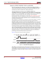
Interaction of PSEN, PSINCDEC, PSCLK, and PSDONE . . . . . . . . . . . . . . . . . . . . . . . .
Phase-Shift Overflow . . . . . . . . . . . . . . . . . . . . . . . . . . . . . . . . . . . . . . . . . . . . . . . . . . .
Phase-Shift Characteristics . . . . . . . . . . . . . . . . . . . . . . . . . . . . . . . . . . . . . . . . . . . . . . .
Dynamic Reconfiguration . . . . . . . . . . . . . . . . . . . . . . . . . . . . . . . . . . . . . . . . . . . . . . . . . .
68
68
69
69
70
70
71
72
72
72
73
73
73
76
77
77
77
Connecting DCMs to Other Clock Resources in Virtex-4 Devices . . . . . . . . . . . . . 78
IBUFG to DCM . . . . . . . . . . . . . . . . . . . . . . . . . . . . . . . . . . . . . . . . . . . . . . . . . . . . . . . . . . .
DCM to BUFGCTRL . . . . . . . . . . . . . . . . . . . . . . . . . . . . . . . . . . . . . . . . . . . . . . . . . . . . . .
BUFGCTRL to DCM . . . . . . . . . . . . . . . . . . . . . . . . . . . . . . . . . . . . . . . . . . . . . . . . . . . . . .
DCM To and From PMCD . . . . . . . . . . . . . . . . . . . . . . . . . . . . . . . . . . . . . . . . . . . . . . . . .
78
78
78
78
Application Examples . . . . . . . . . . . . . . . . . . . . . . . . . . . . . . . . . . . . . . . . . . . . . . . . . . . . . . . 78
Standard Usage . . . . . . . . . . . . . . . . . . . . . . . . . . . . . . . . . . . . . . . . . . . . . . . . . . . . . . . . . .
Board-Level Clock Generation . . . . . . . . . . . . . . . . . . . . . . . . . . . . . . . . . . . . . . . . . . . . . .
Board Deskew with Internal Deskew . . . . . . . . . . . . . . . . . . . . . . . . . . . . . . . . . . . . . . . .
Clock Switching Between Two DCMs . . . . . . . . . . . . . . . . . . . . . . . . . . . . . . . . . . . . . . .
79
79
81
84
VHDL and Verilog Templates, and the Clocking Wizard . . . . . . . . . . . . . . . . . . . . . 84
DCM Timing Models . . . . . . . . . . . . . . . . . . . . . . . . . . . . . . . . . . . . . . . . . . . . . . . . . . . . . . . 88
Reset/Lock . . . . . . . . . . . . . . . . . . . . . . . . . . . . . . . . . . . . . . . . . . . . . . . . . . . . . . . . . . . . . .
Fixed-Phase Shifting . . . . . . . . . . . . . . . . . . . . . . . . . . . . . . . . . . . . . . . . . . . . . . . . . . . . . .
Variable-Phase Shifting . . . . . . . . . . . . . . . . . . . . . . . . . . . . . . . . . . . . . . . . . . . . . . . . . . . .
Status Flags . . . . . . . . . . . . . . . . . . . . . . . . . . . . . . . . . . . . . . . . . . . . . . . . . . . . . . . . . . . . . .
89
90
90
92
Legacy Support . . . . . . . . . . . . . . . . . . . . . . . . . . . . . . . . . . . . . . . . . . . . . . . . . . . . . . . . . . . . . 93
Virtex-4 User Guide
UG070 (v2.0) January 4, 2007
www.xilinx.com
9
R
Chapter 3: Phase-Matched Clock Dividers (PMCDs)
PMCD Summary . . . . . . . . . . . . . . . . . . . . . . . . . . . . . . . . . . . . . . . . . . . . . . . . . . . . . . . . . . . . 95
PMCD Primitives, Ports, and Attributes . . . . . . . . . . . . . . . . . . . . . . . . . . . . . . . . . . . . . 96
PMCD Usage and Design Guidelines . . . . . . . . . . . . . . . . . . . . . . . . . . . . . . . . . . . . . . . . 98
Phase-Matched Divided Clocks . . . . . . . . . . . . . . . . . . . . . . . . . . . . . . . . . . . . . . . . . . . . . 98
Matched Clock Phase . . . . . . . . . . . . . . . . . . . . . . . . . . . . . . . . . . . . . . . . . . . . . . . . . . . . . 98
Reset (RST) and Release (REL) Control Signals . . . . . . . . . . . . . . . . . . . . . . . . . . . . . . . . 99
Connecting PMCD to other Clock Resources . . . . . . . . . . . . . . . . . . . . . . . . . . . . . . . . 101
IBUFG to PMCD . . . . . . . . . . . . . . . . . . . . . . . . . . . . . . . . . . . . . . . . . . . . . . . . . . . . . . 101
DCM to PMCD . . . . . . . . . . . . . . . . . . . . . . . . . . . . . . . . . . . . . . . . . . . . . . . . . . . . . . . 101
BUFGCTRL to PMCD . . . . . . . . . . . . . . . . . . . . . . . . . . . . . . . . . . . . . . . . . . . . . . . . . . 101
PMCD to BUFGCTRL . . . . . . . . . . . . . . . . . . . . . . . . . . . . . . . . . . . . . . . . . . . . . . . . . . 102
PMCD to PMCD . . . . . . . . . . . . . . . . . . . . . . . . . . . . . . . . . . . . . . . . . . . . . . . . . . . . . . 102
Application Examples . . . . . . . . . . . . . . . . . . . . . . . . . . . . . . . . . . . . . . . . . . . . . . . . . . . . . . 102
DCM and a Single PMCD . . . . . . . . . . . . . . . . . . . . . . . . . . . . . . . . . . . . . . . . . . . . . . . . .
DCM and Parallel PMCDs . . . . . . . . . . . . . . . . . . . . . . . . . . . . . . . . . . . . . . . . . . . . . . . .
IBUFG, BUFG, and PMCD . . . . . . . . . . . . . . . . . . . . . . . . . . . . . . . . . . . . . . . . . . . . . . . .
PMCD for Further Division of Clock Frequencies . . . . . . . . . . . . . . . . . . . . . . . . . . . .
102
102
103
104
VHDL and Verilog Templates, and the Clocking Wizard . . . . . . . . . . . . . . . . . . . . 105
VHDL Template . . . . . . . . . . . . . . . . . . . . . . . . . . . . . . . . . . . . . . . . . . . . . . . . . . . . . . . . . 107
Verilog Template . . . . . . . . . . . . . . . . . . . . . . . . . . . . . . . . . . . . . . . . . . . . . . . . . . . . . . . . 108
Chapter 4: Block RAM
Block RAM Summary . . . . . . . . . . . . . . . . . . . . . . . . . . . . . . . . . . . . . . . . . . . . . . . . . . . . . . 111
Additional Virtex-4 Block RAM Features . . . . . . . . . . . . . . . . . . . . . . . . . . . . . . . . . . . . 111
Block RAM Introduction . . . . . . . . . . . . . . . . . . . . . . . . . . . . . . . . . . . . . . . . . . . . . . . . . . . 112
Synchronous Dual-Port and Single-Port RAMs . . . . . . . . . . . . . . . . . . . . . . . . . . . . . 112
Data Flow . . . . . . . . . . . . . . . . . . . . . . . . . . . . . . . . . . . . . . . . . . . . . . . . . . . . . . . . . . . . . .
Read Operation . . . . . . . . . . . . . . . . . . . . . . . . . . . . . . . . . . . . . . . . . . . . . . . . . . . . . . . . .
Write Operation . . . . . . . . . . . . . . . . . . . . . . . . . . . . . . . . . . . . . . . . . . . . . . . . . . . . . . . . .
Operating Modes . . . . . . . . . . . . . . . . . . . . . . . . . . . . . . . . . . . . . . . . . . . . . . . . . . . . . . . .
WRITE_FIRST or Transparent Mode (Default) . . . . . . . . . . . . . . . . . . . . . . . . . . . . . . .
READ_FIRST or Read-Before-Write Mode . . . . . . . . . . . . . . . . . . . . . . . . . . . . . . . . . .
NO_CHANGE Mode . . . . . . . . . . . . . . . . . . . . . . . . . . . . . . . . . . . . . . . . . . . . . . . . . .
Conflict Avoidance . . . . . . . . . . . . . . . . . . . . . . . . . . . . . . . . . . . . . . . . . . . . . . . . . . . . . .
Asynchronous Clocking . . . . . . . . . . . . . . . . . . . . . . . . . . . . . . . . . . . . . . . . . . . . . . . .
Synchronous Clocking . . . . . . . . . . . . . . . . . . . . . . . . . . . . . . . . . . . . . . . . . . . . . . . . .
112
114
114
114
114
115
115
115
116
116
Additional Block RAM Features in Virtex-4 Devices . . . . . . . . . . . . . . . . . . . . . . . . 116
Optional Output Registers . . . . . . . . . . . . . . . . . . . . . . . . . . . . . . . . . . . . . . . . . . . . . . . .
Independent Read and Write Port Width Selection . . . . . . . . . . . . . . . . . . . . . . . . . . .
Cascadable Block RAM . . . . . . . . . . . . . . . . . . . . . . . . . . . . . . . . . . . . . . . . . . . . . . . . . . .
FIFO Support . . . . . . . . . . . . . . . . . . . . . . . . . . . . . . . . . . . . . . . . . . . . . . . . . . . . . . . .
Byte-Wide Write Enable . . . . . . . . . . . . . . . . . . . . . . . . . . . . . . . . . . . . . . . . . . . . . . . . . .
116
117
117
118
119
Block RAM Library Primitives . . . . . . . . . . . . . . . . . . . . . . . . . . . . . . . . . . . . . . . . . . . . . 120
Block RAM Port Signals . . . . . . . . . . . . . . . . . . . . . . . . . . . . . . . . . . . . . . . . . . . . . . . . . . . . 121
Clock - CLK[A|B] . . . . . . . . . . . . . . . . . . . . . . . . . . . . . . . . . . . . . . . . . . . . . . . . . . . . . . .
Enable - EN[A|B] . . . . . . . . . . . . . . . . . . . . . . . . . . . . . . . . . . . . . . . . . . . . . . . . . . . . . . . .
Write Enable - WE[A|B] . . . . . . . . . . . . . . . . . . . . . . . . . . . . . . . . . . . . . . . . . . . . . . . . . .
Register Enable - REGCE[A|B] . . . . . . . . . . . . . . . . . . . . . . . . . . . . . . . . . . . . . . . . . . . .
Set/Reset - SSR[A|B] . . . . . . . . . . . . . . . . . . . . . . . . . . . . . . . . . . . . . . . . . . . . . . . . . . . .
10
www.xilinx.com
121
121
121
122
122
Virtex-4 User Guide
UG070 (v2.0) January 4, 2007
R
Address Bus - ADDR[A|B]<14:#> . . . . . . . . . . . . . . . . . . . . . . . . . . . . . . . . . . . . . . . . .
Data-In Buses - DI[A|B]<#:0> & DIP[A|B]<#:0> . . . . . . . . . . . . . . . . . . . . . . . . . . . . .
Data-Out Buses - DO[A|B]<#:0> and DOP[A|B]<#:0> . . . . . . . . . . . . . . . . . . . . . . . .
Cascade - CASCADEIN[A|B] . . . . . . . . . . . . . . . . . . . . . . . . . . . . . . . . . . . . . . . . . . . . .
Cascade - CASCADEOUT[A|B] . . . . . . . . . . . . . . . . . . . . . . . . . . . . . . . . . . . . . . . . . . .
Inverting Control Pins . . . . . . . . . . . . . . . . . . . . . . . . . . . . . . . . . . . . . . . . . . . . . . . . . . . .
GSR . . . . . . . . . . . . . . . . . . . . . . . . . . . . . . . . . . . . . . . . . . . . . . . . . . . . . . . . . . . . . . . . . . . .
Unused Inputs . . . . . . . . . . . . . . . . . . . . . . . . . . . . . . . . . . . . . . . . . . . . . . . . . . . . . . . . . .
122
122
123
123
123
123
123
123
Block RAM Address Mapping . . . . . . . . . . . . . . . . . . . . . . . . . . . . . . . . . . . . . . . . . . . . . . 123
Block RAM Attributes . . . . . . . . . . . . . . . . . . . . . . . . . . . . . . . . . . . . . . . . . . . . . . . . . . . . . 124
Content Initialization - INIT_xx . . . . . . . . . . . . . . . . . . . . . . . . . . . . . . . . . . . . . . . . . . . .
Content Initialization - INITP_xx . . . . . . . . . . . . . . . . . . . . . . . . . . . . . . . . . . . . . . . . . .
Output Latches Initialization - INIT (INIT_A & INIT_B) . . . . . . . . . . . . . . . . . . . . . .
Output Latches Synchronous Set/Reset - SRVAL (SRVAL_A & SRVAL_B) . . . . . .
Optional Output Register On/Off Switch - DO[A|B]_REG . . . . . . . . . . . . . . . . . . . .
Clock Inversion at Output Register Switch - INVERT_CLK_DO[A|B]_REG . . . . .
Extended Mode Address Determinant - RAM_EXTENSION_[A|B] . . . . . . . . . . . .
Read Width - READ_WIDTH_[A|B] . . . . . . . . . . . . . . . . . . . . . . . . . . . . . . . . . . . . . . .
Write Width - WRITE_WIDTH_[A|B] . . . . . . . . . . . . . . . . . . . . . . . . . . . . . . . . . . . . . .
Write Mode - WRITE_MODE_[A|B] . . . . . . . . . . . . . . . . . . . . . . . . . . . . . . . . . . . . . . .
Block RAM Location Constraints . . . . . . . . . . . . . . . . . . . . . . . . . . . . . . . . . . . . . . . . . .
124
125
125
125
126
126
126
126
126
126
126
Block RAM Initialization in VHDL or Verilog Code . . . . . . . . . . . . . . . . . . . . . . . . 127
Block RAM VHDL and Verilog Templates. . . . . . . . . . . . . . . . . . . . . . . . . . . . . . . . . . 127
RAMB16 VHDL Template . . . . . . . . . . . . . . . . . . . . . . . . . . . . . . . . . . . . . . . . . . . . . . . . 127
RAMB16 Verilog Template . . . . . . . . . . . . . . . . . . . . . . . . . . . . . . . . . . . . . . . . . . . . . . . . 131
Additional RAMB16 Primitive Design Considerations . . . . . . . . . . . . . . . . . . . . . . 136
Data Parity Buses - DIP[A/B] and DOP[A/B] . . . . . . . . . . . . . . . . . . . . . . . . . . . . . . .
Optional Output Registers . . . . . . . . . . . . . . . . . . . . . . . . . . . . . . . . . . . . . . . . . . . . . . . .
Independent Read and Write Port Width . . . . . . . . . . . . . . . . . . . . . . . . . . . . . . . . . . .
RAMB16 Port Mapping Design Rules . . . . . . . . . . . . . . . . . . . . . . . . . . . . . . . . . . . . . .
Cascadeable Block RAM . . . . . . . . . . . . . . . . . . . . . . . . . . . . . . . . . . . . . . . . . . . . . . . . . .
Byte-Write Enable . . . . . . . . . . . . . . . . . . . . . . . . . . . . . . . . . . . . . . . . . . . . . . . . . . . . . . .
136
136
136
136
137
137
Additional Block RAM Primitives . . . . . . . . . . . . . . . . . . . . . . . . . . . . . . . . . . . . . . . . . . 137
Instantiation of Additional Block RAM Primitives . . . . . . . . . . . . . . . . . . . . . . . . . . . . 140
Block RAM Applications . . . . . . . . . . . . . . . . . . . . . . . . . . . . . . . . . . . . . . . . . . . . . . . . . . . 140
Creating Larger RAM Structures . . . . . . . . . . . . . . . . . . . . . . . . . . . . . . . . . . . . . . . . . . . 140
Block RAM Timing Model . . . . . . . . . . . . . . . . . . . . . . . . . . . . . . . . . . . . . . . . . . . . . . . . . 140
Block RAM Timing Parameters . . . . . . . . . . . . . . . . . . . . . . . . . . . . . . . . . . . . . . . . . . . .
Block RAM Timing Characteristics . . . . . . . . . . . . . . . . . . . . . . . . . . . . . . . . . . . . . . . . .
Clock Event 1 . . . . . . . . . . . . . . . . . . . . . . . . . . . . . . . . . . . . . . . . . . . . . . . . . . . . . . . .
Clock Event 2 . . . . . . . . . . . . . . . . . . . . . . . . . . . . . . . . . . . . . . . . . . . . . . . . . . . . . . . .
Clock Event 4 . . . . . . . . . . . . . . . . . . . . . . . . . . . . . . . . . . . . . . . . . . . . . . . . . . . . . . . .
Clock Event 5 . . . . . . . . . . . . . . . . . . . . . . . . . . . . . . . . . . . . . . . . . . . . . . . . . . . . . . . .
Block RAM Timing Model . . . . . . . . . . . . . . . . . . . . . . . . . . . . . . . . . . . . . . . . . . . . . . . .
140
141
142
142
143
143
143
Built-in FIFO Support . . . . . . . . . . . . . . . . . . . . . . . . . . . . . . . . . . . . . . . . . . . . . . . . . . . . . . 144
EMPTY Latency . . . . . . . . . . . . . . . . . . . . . . . . . . . . . . . . . . . . . . . . . . . . . . . . . . . . . . 145
Top-Level View of FIFO Architecture . . . . . . . . . . . . . . . . . . . . . . . . . . . . . . . . . . . . . . .
FIFO Primitive . . . . . . . . . . . . . . . . . . . . . . . . . . . . . . . . . . . . . . . . . . . . . . . . . . . . . . . . . . . . .
FIFO Port Descriptions . . . . . . . . . . . . . . . . . . . . . . . . . . . . . . . . . . . . . . . . . . . . . . . . . . . . .
FIFO Operations . . . . . . . . . . . . . . . . . . . . . . . . . . . . . . . . . . . . . . . . . . . . . . . . . . . . . . . . . . .
Virtex-4 User Guide
UG070 (v2.0) January 4, 2007
www.xilinx.com
146
146
147
148
11
R
Reset . . . . . . . . . . . . . . . . . . . . . . . . . . . . . . . . . . . . . . . . . . . . . . . . . . . . . . . . . . . . . . . . . . .
Operating Mode . . . . . . . . . . . . . . . . . . . . . . . . . . . . . . . . . . . . . . . . . . . . . . . . . . . . . . . . .
Standard Mode . . . . . . . . . . . . . . . . . . . . . . . . . . . . . . . . . . . . . . . . . . . . . . . . . . . . . . .
First Word Fall Through (FWFT) Mode . . . . . . . . . . . . . . . . . . . . . . . . . . . . . . . . . . . .
Status Flags . . . . . . . . . . . . . . . . . . . . . . . . . . . . . . . . . . . . . . . . . . . . . . . . . . . . . . . . . . . . .
Empty Flag . . . . . . . . . . . . . . . . . . . . . . . . . . . . . . . . . . . . . . . . . . . . . . . . . . . . . . . . . .
Almost Empty Flag . . . . . . . . . . . . . . . . . . . . . . . . . . . . . . . . . . . . . . . . . . . . . . . . . . . .
Read Error Flag . . . . . . . . . . . . . . . . . . . . . . . . . . . . . . . . . . . . . . . . . . . . . . . . . . . . . . .
Full Flag . . . . . . . . . . . . . . . . . . . . . . . . . . . . . . . . . . . . . . . . . . . . . . . . . . . . . . . . . . . .
Write Error Flag . . . . . . . . . . . . . . . . . . . . . . . . . . . . . . . . . . . . . . . . . . . . . . . . . . . . . .
Almost Full Flag . . . . . . . . . . . . . . . . . . . . . . . . . . . . . . . . . . . . . . . . . . . . . . . . . . . . . .
148
148
148
148
148
148
149
149
149
149
149
FIFO Attributes . . . . . . . . . . . . . . . . . . . . . . . . . . . . . . . . . . . . . . . . . . . . . . . . . . . . . . . . . . . . 150
FIFO Almost Full/Empty Flag Offset Range . . . . . . . . . . . . . . . . . . . . . . . . . . . . . . . . . 150
FIFO VHDL and Verilog Templates . . . . . . . . . . . . . . . . . . . . . . . . . . . . . . . . . . . . . . . . 151
FIFO VHDL Template . . . . . . . . . . . . . . . . . . . . . . . . . . . . . . . . . . . . . . . . . . . . . . . . . . . . 151
FIFO Verilog Template . . . . . . . . . . . . . . . . . . . . . . . . . . . . . . . . . . . . . . . . . . . . . . . . . . . 152
FIFO Timing Models and Parameters . . . . . . . . . . . . . . . . . . . . . . . . . . . . . . . . . . . . . . . 153
FIFO Timing Characteristics . . . . . . . . . . . . . . . . . . . . . . . . . . . . . . . . . . . . . . . . . . . . . . .
Case 1: Writing to an Empty FIFO . . . . . . . . . . . . . . . . . . . . . . . . . . . . . . . . . . . . . . . .
Case 2: Writing to a Full or Almost Full FIFO . . . . . . . . . . . . . . . . . . . . . . . . . . . . . . . .
Case 3: Reading From a Full FIFO . . . . . . . . . . . . . . . . . . . . . . . . . . . . . . . . . . . . . . . .
Case 4: Reading From An Empty or Almost Empty FIFO . . . . . . . . . . . . . . . . . . . . . .
Case 5: Resetting All Flags . . . . . . . . . . . . . . . . . . . . . . . . . . . . . . . . . . . . . . . . . . . . . .
154
155
156
157
159
160
FIFO Applications . . . . . . . . . . . . . . . . . . . . . . . . . . . . . . . . . . . . . . . . . . . . . . . . . . . . . . . . . 160
Cascading FIFOs to Increase Depth . . . . . . . . . . . . . . . . . . . . . . . . . . . . . . . . . . . . . . . . 161
Cascading FIFOs to Increase Width . . . . . . . . . . . . . . . . . . . . . . . . . . . . . . . . . . . . . . . . 161
Built-in Block RAM Error Correction Code . . . . . . . . . . . . . . . . . . . . . . . . . . . . . . . . . 162
Top-Level View of the Block RAM ECC Architecture . . . . . . . . . . . . . . . . . . . . . . . . .
Block RAM ECC Primitive . . . . . . . . . . . . . . . . . . . . . . . . . . . . . . . . . . . . . . . . . . . . . . . .
Block RAM ECC Port Description . . . . . . . . . . . . . . . . . . . . . . . . . . . . . . . . . . . . . . . . . .
Error Status Description . . . . . . . . . . . . . . . . . . . . . . . . . . . . . . . . . . . . . . . . . . . . . . . . . .
Block RAM ECC Attribute . . . . . . . . . . . . . . . . . . . . . . . . . . . . . . . . . . . . . . . . . . . . . . . .
Block RAM ECC VHDL and Verilog Templates . . . . . . . . . . . . . . . . . . . . . . . . . . . . . .
Block RAM ECC VHDL Template . . . . . . . . . . . . . . . . . . . . . . . . . . . . . . . . . . . . . . . .
Block RAM ECC Verilog Template . . . . . . . . . . . . . . . . . . . . . . . . . . . . . . . . . . . . . . . .
162
163
163
164
164
164
164
165
Chapter 5: Configurable Logic Blocks (CLBs)
CLB Overview . . . . . . . . . . . . . . . . . . . . . . . . . . . . . . . . . . . . . . . . . . . . . . . . . . . . . . . . . . . . . 167
Slice Description . . . . . . . . . . . . . . . . . . . . . . . . . . . . . . . . . . . . . . . . . . . . . . . . . . . . . . . . .
CLB/Slice Configurations . . . . . . . . . . . . . . . . . . . . . . . . . . . . . . . . . . . . . . . . . . . . . . .
Look-Up Table (LUT) . . . . . . . . . . . . . . . . . . . . . . . . . . . . . . . . . . . . . . . . . . . . . . . . . .
Storage Elements. . . . . . . . . . . . . . . . . . . . . . . . . . . . . . . . . . . . . . . . . . . . . . . . . . . . . .
Distributed RAM and Memory (Available in SLICEM only) . . . . . . . . . . . . . . . . . . . .
Read Only Memory (ROM). . . . . . . . . . . . . . . . . . . . . . . . . . . . . . . . . . . . . . . . . . . . . .
Shift Registers (Available in SLICEM only) . . . . . . . . . . . . . . . . . . . . . . . . . . . . . . . . .
Shift Register Data Flow . . . . . . . . . . . . . . . . . . . . . . . . . . . . . . . . . . . . . . . . . . . . . . . .
Multiplexers . . . . . . . . . . . . . . . . . . . . . . . . . . . . . . . . . . . . . . . . . . . . . . . . . . . . . . . . .
Designing Large Multiplexers. . . . . . . . . . . . . . . . . . . . . . . . . . . . . . . . . . . . . . . . . . . .
Fast Lookahead Carry Logic . . . . . . . . . . . . . . . . . . . . . . . . . . . . . . . . . . . . . . . . . . . . .
Arithmetic Logic . . . . . . . . . . . . . . . . . . . . . . . . . . . . . . . . . . . . . . . . . . . . . . . . . . . . . .
168
168
172
172
173
176
177
180
181
183
187
189
CLB / Slice Timing Models . . . . . . . . . . . . . . . . . . . . . . . . . . . . . . . . . . . . . . . . . . . . . . . . . 189
12
www.xilinx.com
Virtex-4 User Guide
UG070 (v2.0) January 4, 2007
R
General Slice Timing Model and Parameters . . . . . . . . . . . . . . . . . . . . . . . . . . . . . . . .
Timing Parameters . . . . . . . . . . . . . . . . . . . . . . . . . . . . . . . . . . . . . . . . . . . . . . . . . . . .
Timing Characteristics . . . . . . . . . . . . . . . . . . . . . . . . . . . . . . . . . . . . . . . . . . . . . . . . .
Slice Distributed RAM Timing Model and Parameters
(Available in SLICEM only) . . . . . . . . . . . . . . . . . . . . . . . . . . . . . . . . . . . . . . . . . . . . .
Distributed RAM Timing Parameters . . . . . . . . . . . . . . . . . . . . . . . . . . . . . . . . . . . . . .
Distributed RAM Timing Characteristics . . . . . . . . . . . . . . . . . . . . . . . . . . . . . . . . . . .
Slice SRL Timing Model and Parameters (Available in SLICEM only) . . . . . . . . . . .
Slice SRL Timing Parameters . . . . . . . . . . . . . . . . . . . . . . . . . . . . . . . . . . . . . . . . . . . .
Slice SRL Timing Characteristics. . . . . . . . . . . . . . . . . . . . . . . . . . . . . . . . . . . . . . . . . .
Slice Carry-Chain Timing Model and Parameters . . . . . . . . . . . . . . . . . . . . . . . . . . . .
Slice Carry-Chain Timing Parameters. . . . . . . . . . . . . . . . . . . . . . . . . . . . . . . . . . . . . .
Slice Carry-Chain Timing Characteristics . . . . . . . . . . . . . . . . . . . . . . . . . . . . . . . . . . .
190
190
192
193
194
194
196
197
197
198
200
200
CLB Primitives and Verilog/VHDL Examples . . . . . . . . . . . . . . . . . . . . . . . . . . . . . . . 201
Distributed RAM Primitives . . . . . . . . . . . . . . . . . . . . . . . . . . . . . . . . . . . . . . . . . . . . . .
VHDL and Verilog Instantiations . . . . . . . . . . . . . . . . . . . . . . . . . . . . . . . . . . . . . . . . . .
Port Signals . . . . . . . . . . . . . . . . . . . . . . . . . . . . . . . . . . . . . . . . . . . . . . . . . . . . . . . . . . . . .
Clock - WCLK . . . . . . . . . . . . . . . . . . . . . . . . . . . . . . . . . . . . . . . . . . . . . . . . . . . . . . . .
Enable - WE . . . . . . . . . . . . . . . . . . . . . . . . . . . . . . . . . . . . . . . . . . . . . . . . . . . . . . . . .
Address - A0, A1, A2, A3 (A4, A5) . . . . . . . . . . . . . . . . . . . . . . . . . . . . . . . . . . . . . . . .
Data In - D. . . . . . . . . . . . . . . . . . . . . . . . . . . . . . . . . . . . . . . . . . . . . . . . . . . . . . . . . . .
Data Out - O, SPO, and DPO . . . . . . . . . . . . . . . . . . . . . . . . . . . . . . . . . . . . . . . . . . . .
Inverting Control Pins . . . . . . . . . . . . . . . . . . . . . . . . . . . . . . . . . . . . . . . . . . . . . . . . .
Global Set/Reset - GSR . . . . . . . . . . . . . . . . . . . . . . . . . . . . . . . . . . . . . . . . . . . . . . . . .
Attributes. . . . . . . . . . . . . . . . . . . . . . . . . . . . . . . . . . . . . . . . . . . . . . . . . . . . . . . . . . . . . . .
Content Initialization - INIT . . . . . . . . . . . . . . . . . . . . . . . . . . . . . . . . . . . . . . . . . . . . .
Initialization in VHDL or Verilog Codes . . . . . . . . . . . . . . . . . . . . . . . . . . . . . . . . . . .
Location Constraints . . . . . . . . . . . . . . . . . . . . . . . . . . . . . . . . . . . . . . . . . . . . . . . . . . .
Creating Larger RAM Structures . . . . . . . . . . . . . . . . . . . . . . . . . . . . . . . . . . . . . . . . .
VHDL and Verilog Templates . . . . . . . . . . . . . . . . . . . . . . . . . . . . . . . . . . . . . . . . . . .
201
202
202
202
202
202
202
202
202
202
203
203
203
203
204
204
Shift Registers (SRLs) Primitives and Verilog/VHDL Example . . . . . . . . . . . . . . 206
SRL Primitives and Submodules . . . . . . . . . . . . . . . . . . . . . . . . . . . . . . . . . . . . . . . . . . .
Initialization in VHDL or Verilog Code . . . . . . . . . . . . . . . . . . . . . . . . . . . . . . . . . . . . .
Port Signals . . . . . . . . . . . . . . . . . . . . . . . . . . . . . . . . . . . . . . . . . . . . . . . . . . . . . . . . . . . . .
Clock - CLK. . . . . . . . . . . . . . . . . . . . . . . . . . . . . . . . . . . . . . . . . . . . . . . . . . . . . . . . . .
Data In - D. . . . . . . . . . . . . . . . . . . . . . . . . . . . . . . . . . . . . . . . . . . . . . . . . . . . . . . . . . .
Clock Enable - CE (optional) . . . . . . . . . . . . . . . . . . . . . . . . . . . . . . . . . . . . . . . . . . . . .
Address - A0, A1, A2, A3 . . . . . . . . . . . . . . . . . . . . . . . . . . . . . . . . . . . . . . . . . . . . . . .
Data Out - Q . . . . . . . . . . . . . . . . . . . . . . . . . . . . . . . . . . . . . . . . . . . . . . . . . . . . . . . . .
Data Out - Q15 (optional) . . . . . . . . . . . . . . . . . . . . . . . . . . . . . . . . . . . . . . . . . . . . . . .
Inverting Control Pins . . . . . . . . . . . . . . . . . . . . . . . . . . . . . . . . . . . . . . . . . . . . . . . . .
Global Set/Reset - GSR . . . . . . . . . . . . . . . . . . . . . . . . . . . . . . . . . . . . . . . . . . . . . . . . .
Attributes. . . . . . . . . . . . . . . . . . . . . . . . . . . . . . . . . . . . . . . . . . . . . . . . . . . . . . . . . . . . . . .
Content Initialization - INIT . . . . . . . . . . . . . . . . . . . . . . . . . . . . . . . . . . . . . . . . . . . . .
Location Constraints . . . . . . . . . . . . . . . . . . . . . . . . . . . . . . . . . . . . . . . . . . . . . . . . . . . . .
Fully Synchronous Shift Registers . . . . . . . . . . . . . . . . . . . . . . . . . . . . . . . . . . . . . . . . . .
Static-Length Shift Registers . . . . . . . . . . . . . . . . . . . . . . . . . . . . . . . . . . . . . . . . . . . . . . .
VHDL and Verilog Instantiation . . . . . . . . . . . . . . . . . . . . . . . . . . . . . . . . . . . . . . . . . . .
VHDL and Verilog Templates . . . . . . . . . . . . . . . . . . . . . . . . . . . . . . . . . . . . . . . . . . .
206
208
208
208
208
208
208
208
208
208
208
209
209
209
210
210
211
211
Multiplexer Primitives and Verilog/VHDL Examples . . . . . . . . . . . . . . . . . . . . . . . 213
Multiplexer Primitives and Submodules . . . . . . . . . . . . . . . . . . . . . . . . . . . . . . . . . . . . 213
Port Signals . . . . . . . . . . . . . . . . . . . . . . . . . . . . . . . . . . . . . . . . . . . . . . . . . . . . . . . . . . . . . 214
Data In - DATA_I . . . . . . . . . . . . . . . . . . . . . . . . . . . . . . . . . . . . . . . . . . . . . . . . . . . . . 214
Virtex-4 User Guide
UG070 (v2.0) January 4, 2007
www.xilinx.com
13
R
Control In - SELECT_I . . . . . . . . . . . . . . . . . . . . . . . . . . . . . . . . . . . . . . . . . . . . . . . . . 214
Data Out - DATA_O . . . . . . . . . . . . . . . . . . . . . . . . . . . . . . . . . . . . . . . . . . . . . . . . . . . 214
Multiplexer Verilog/VHDL Examples . . . . . . . . . . . . . . . . . . . . . . . . . . . . . . . . . . . . . . 214
VHDL and Verilog Instantiation . . . . . . . . . . . . . . . . . . . . . . . . . . . . . . . . . . . . . . . . . . 214
VHDL and Verilog Submodules . . . . . . . . . . . . . . . . . . . . . . . . . . . . . . . . . . . . . . . . . . 214
Chapter 6: SelectIO Resources
I/O Tile Overview . . . . . . . . . . . . . . . . . . . . . . . . . . . . . . . . . . . . . . . . . . . . . . . . . . . . . . . . . . 219
SelectIO Resources Introduction . . . . . . . . . . . . . . . . . . . . . . . . . . . . . . . . . . . . . . . . . . . 220
SelectIO Resources General Guidelines . . . . . . . . . . . . . . . . . . . . . . . . . . . . . . . . . . . . 220
Virtex-4 I/O Bank Rules . . . . . . . . . . . . . . . . . . . . . . . . . . . . . . . . . . . . . . . . . . . . . . . . . .
3.3V I/O Support . . . . . . . . . . . . . . . . . . . . . . . . . . . . . . . . . . . . . . . . . . . . . . . . . . . . .
Reference Voltage (VREF) Pins . . . . . . . . . . . . . . . . . . . . . . . . . . . . . . . . . . . . . . . . . . .
Output Drive Source Voltage (VCCO) Pins . . . . . . . . . . . . . . . . . . . . . . . . . . . . . . . . . .
Virtex-4 Digitally Controlled Impedance (DCI) . . . . . . . . . . . . . . . . . . . . . . . . . . . . . .
Introduction . . . . . . . . . . . . . . . . . . . . . . . . . . . . . . . . . . . . . . . . . . . . . . . . . . . . . . . . .
Xilinx DCI . . . . . . . . . . . . . . . . . . . . . . . . . . . . . . . . . . . . . . . . . . . . . . . . . . . . . . . . . . .
Controlled Impedance Driver (Source Termination) . . . . . . . . . . . . . . . . . . . . . . . . . .
Controlled Impedance Driver with Half Impedance (Source Termination) . . . . . . . . .
Input Termination to VCCO (Single Termination) . . . . . . . . . . . . . . . . . . . . . . . . . . . .
Input Termination to VCCO/2 (Split Termination) . . . . . . . . . . . . . . . . . . . . . . . . . . .
Driver with Termination to VCCO (Single Termination) . . . . . . . . . . . . . . . . . . . . . . . .
Driver with Termination to VCCO /2 (Split Termination) . . . . . . . . . . . . . . . . . . . . . . .
DCI in Virtex-4 Hardware . . . . . . . . . . . . . . . . . . . . . . . . . . . . . . . . . . . . . . . . . . . . . . . .
DCI Usage Examples . . . . . . . . . . . . . . . . . . . . . . . . . . . . . . . . . . . . . . . . . . . . . . . . . .
220
221
221
221
222
222
222
223
223
224
225
226
227
227
228
Virtex-4 SelectIO Primitives . . . . . . . . . . . . . . . . . . . . . . . . . . . . . . . . . . . . . . . . . . . . . . . . 231
IBUF and IBUFG . . . . . . . . . . . . . . . . . . . . . . . . . . . . . . . . . . . . . . . . . . . . . . . . . . . . . . . .
OBUF . . . . . . . . . . . . . . . . . . . . . . . . . . . . . . . . . . . . . . . . . . . . . . . . . . . . . . . . . . . . . . . . . .
OBUFT . . . . . . . . . . . . . . . . . . . . . . . . . . . . . . . . . . . . . . . . . . . . . . . . . . . . . . . . . . . . . . . . .
IOBUF . . . . . . . . . . . . . . . . . . . . . . . . . . . . . . . . . . . . . . . . . . . . . . . . . . . . . . . . . . . . . . . . .
IBUFDS and IBUFGDS . . . . . . . . . . . . . . . . . . . . . . . . . . . . . . . . . . . . . . . . . . . . . . . . . . .
OBUFDS . . . . . . . . . . . . . . . . . . . . . . . . . . . . . . . . . . . . . . . . . . . . . . . . . . . . . . . . . . . . . . .
OBUFTDS . . . . . . . . . . . . . . . . . . . . . . . . . . . . . . . . . . . . . . . . . . . . . . . . . . . . . . . . . . . . . .
IOBUFDS . . . . . . . . . . . . . . . . . . . . . . . . . . . . . . . . . . . . . . . . . . . . . . . . . . . . . . . . . . . . . . .
Virtex-4 SelectIO Attributes/Constraints . . . . . . . . . . . . . . . . . . . . . . . . . . . . . . . . . . . .
Location Constraints . . . . . . . . . . . . . . . . . . . . . . . . . . . . . . . . . . . . . . . . . . . . . . . . . . .
IOStandard Attribute . . . . . . . . . . . . . . . . . . . . . . . . . . . . . . . . . . . . . . . . . . . . . . . . . .
Output Slew Rate Attributes . . . . . . . . . . . . . . . . . . . . . . . . . . . . . . . . . . . . . . . . . . . . .
Output Drive Strength Attributes . . . . . . . . . . . . . . . . . . . . . . . . . . . . . . . . . . . . . . . . .
Lower Capacitance I/O Attributes . . . . . . . . . . . . . . . . . . . . . . . . . . . . . . . . . . . . . . . .
PULLUP/PULLDOWN/KEEPER for IBUF, OBUFT, and IOBUF . . . . . . . . . . . . . . . .
Differential Termination Attribute . . . . . . . . . . . . . . . . . . . . . . . . . . . . . . . . . . . . . . . .
Virtex-4 I/O Resource VHDL/Verilog Examples . . . . . . . . . . . . . . . . . . . . . . . . . . . . .
VHDL Template . . . . . . . . . . . . . . . . . . . . . . . . . . . . . . . . . . . . . . . . . . . . . . . . . . . . . .
Verilog Template . . . . . . . . . . . . . . . . . . . . . . . . . . . . . . . . . . . . . . . . . . . . . . . . . . . . .
232
232
232
233
233
233
234
234
234
234
235
235
235
235
236
236
236
236
237
Specific Guidelines for Virtex-4 I/O Supported Standards . . . . . . . . . . . . . . . . . . 237
LVTTL (Low Voltage Transistor-Transistor Logic) . . . . . . . . . . . . . . . . . . . . . . . . . . .
LVCMOS (Low Voltage Complementary Metal Oxide Semiconductor). . . . . . . . . .
LVDCI (Low Voltage Digitally Controlled Impedance) . . . . . . . . . . . . . . . . . . . . . . . .
LVDCI_DV2 . . . . . . . . . . . . . . . . . . . . . . . . . . . . . . . . . . . . . . . . . . . . . . . . . . . . . . . . .
HSLVDCI (High-Speed Low Voltage Digitally Controlled Impedance) . . . . . . . . . . . .
PCIX, PCI33, PCI66 (Peripheral Component Interface) . . . . . . . . . . . . . . . . . . . . . . . .
14
www.xilinx.com
238
240
242
242
244
245
Virtex-4 User Guide
UG070 (v2.0) January 4, 2007
R
GTL (Gunning Transceiver Logic) . . . . . . . . . . . . . . . . . . . . . . . . . . . . . . . . . . . . . . . . . .
GTL_DCI Usage . . . . . . . . . . . . . . . . . . . . . . . . . . . . . . . . . . . . . . . . . . . . . . . . . . . . . .
GTLP (Gunning Transceiver Logic Plus) . . . . . . . . . . . . . . . . . . . . . . . . . . . . . . . . . . . .
GTLP_DCI Usage . . . . . . . . . . . . . . . . . . . . . . . . . . . . . . . . . . . . . . . . . . . . . . . . . . . . .
HSTL (High-Speed Transceiver Logic) . . . . . . . . . . . . . . . . . . . . . . . . . . . . . . . . . . . . . .
HSTL_ I, HSTL_ III, HSTL_ I_18, HSTL_ III_18 Usage . . . . . . . . . . . . . . . . . . . . . . . . .
HSTL_ I_DCI, HSTL_ III_DCI, HSTL_ I_DCI_18, HSTL_ III_DCI_18 Usage . . . . . . . .
HSTL_ II, HSTL_ IV, HSTL_ II_18, HSTL_ IV_18 Usage . . . . . . . . . . . . . . . . . . . . . . . .
HSTL_ II_DCI, HSTL_ IV_DCI, HSTL_ II_DCI_18, HSTL_ IV_DCI_18 Usage . . . . . . .
DIFF_HSTL_ II, DIFF_HSTL_II_18 . . . . . . . . . . . . . . . . . . . . . . . . . . . . . . . . . . . . . . . .
DIFF_HSTL_II_DCI, DIFF_HSTL_II_DCI_18 . . . . . . . . . . . . . . . . . . . . . . . . . . . . . . . .
HSTL Class I . . . . . . . . . . . . . . . . . . . . . . . . . . . . . . . . . . . . . . . . . . . . . . . . . . . . . . . . . . . .
HSTL Class II . . . . . . . . . . . . . . . . . . . . . . . . . . . . . . . . . . . . . . . . . . . . . . . . . . . . . . . . . . .
Complementary Single-Ended (CSE) Differential HSTL Class II . . . . . . . . . . . . . . . .
HSTL Class III . . . . . . . . . . . . . . . . . . . . . . . . . . . . . . . . . . . . . . . . . . . . . . . . . . . . . . . . . . .
HSTL Class IV . . . . . . . . . . . . . . . . . . . . . . . . . . . . . . . . . . . . . . . . . . . . . . . . . . . . . . . . . . .
HSTL Class I (1.8V) . . . . . . . . . . . . . . . . . . . . . . . . . . . . . . . . . . . . . . . . . . . . . . . . . . . . . .
HSTL Class II (1.8V) . . . . . . . . . . . . . . . . . . . . . . . . . . . . . . . . . . . . . . . . . . . . . . . . . . . . . .
Complementary Single-Ended (CSE) Differential HSTL Class II (1.8V) . . . . . . . . . .
HSTL Class III (1.8V) . . . . . . . . . . . . . . . . . . . . . . . . . . . . . . . . . . . . . . . . . . . . . . . . . . . . .
HSTL Class IV (1.8V) . . . . . . . . . . . . . . . . . . . . . . . . . . . . . . . . . . . . . . . . . . . . . . . . . . . . .
SSTL (Stub-Series Terminated Logic) . . . . . . . . . . . . . . . . . . . . . . . . . . . . . . . . . . . . . . .
SSTL2_I, SSTL18_I Usage . . . . . . . . . . . . . . . . . . . . . . . . . . . . . . . . . . . . . . . . . . . . . . .
SSTL2_I_DCI, SSTL18_I_DCI Usage . . . . . . . . . . . . . . . . . . . . . . . . . . . . . . . . . . . . . . .
SSTL2_II, SSTL18_II Usage . . . . . . . . . . . . . . . . . . . . . . . . . . . . . . . . . . . . . . . . . . . . . .
SSTL2_II_DCI, SSTL18_II_DCI Usage . . . . . . . . . . . . . . . . . . . . . . . . . . . . . . . . . . . . . .
DIFF_SSTL2_II, DIFF_SSTL18_II Usage . . . . . . . . . . . . . . . . . . . . . . . . . . . . . . . . . . . .
DIFF_SSTL2_II_DCI, DIFF_SSTL18_II_DCI Usage . . . . . . . . . . . . . . . . . . . . . . . . . . . .
SSTL2 Class I (2.5V) . . . . . . . . . . . . . . . . . . . . . . . . . . . . . . . . . . . . . . . . . . . . . . . . . . . . . .
SSTL2 Class II (2.5V) . . . . . . . . . . . . . . . . . . . . . . . . . . . . . . . . . . . . . . . . . . . . . . . . . . . . .
Complementary Single-Ended (CSE) Differential SSTL2 Class II (2.5V) . . . . . . . . . .
SSTL18 Class I (1.8V) . . . . . . . . . . . . . . . . . . . . . . . . . . . . . . . . . . . . . . . . . . . . . . . . . . . . .
SSTL18 Class II (1.8V) . . . . . . . . . . . . . . . . . . . . . . . . . . . . . . . . . . . . . . . . . . . . . . . . . . . .
Complementary Single-Ended (CSE) Differential SSTL Class II (1.8V) . . . . . . . . . . .
Differential Termination: DIFF_TERM Attribute . . . . . . . . . . . . . . . . . . . . . . . . . . . . .
LVDS and Extended LVDS (Low Voltage Differential Signaling) . . . . . . . . . . . . . . .
Transmitter Termination . . . . . . . . . . . . . . . . . . . . . . . . . . . . . . . . . . . . . . . . . . . . . . . .
Receiver Termination . . . . . . . . . . . . . . . . . . . . . . . . . . . . . . . . . . . . . . . . . . . . . . . . . .
HyperTransport™ Protocol (LDT) . . . . . . . . . . . . . . . . . . . . . . . . . . . . . . . . . . . . . . . . .
BLVDS (Bus LVDS) . . . . . . . . . . . . . . . . . . . . . . . . . . . . . . . . . . . . . . . . . . . . . . . . . . . . . .
CSE Differential LVPECL (Low-Voltage Positive Emitter-Coupled Logic) . . . . . . .
LVPECL Transceiver Termination . . . . . . . . . . . . . . . . . . . . . . . . . . . . . . . . . . . . . . . .
246
246
247
248
249
249
249
249
249
249
250
250
251
253
256
257
259
260
262
265
266
268
268
268
269
269
269
269
270
271
273
276
277
279
282
282
283
283
284
285
285
286
Rules for Combining I/O Standards in the Same Bank . . . . . . . . . . . . . . . . . . . . . . 286
3.3V I/O Design Guidelines . . . . . . . . . . . . . . . . . . . . . . . . . . . . . . . . . . . . . . . . . . . . . . .
I/O Standard Design Rules. . . . . . . . . . . . . . . . . . . . . . . . . . . . . . . . . . . . . . . . . . . . . .
Mixing Techniques . . . . . . . . . . . . . . . . . . . . . . . . . . . . . . . . . . . . . . . . . . . . . . . . . . . .
Summary . . . . . . . . . . . . . . . . . . . . . . . . . . . . . . . . . . . . . . . . . . . . . . . . . . . . . . . . . . .
290
290
293
294
Simultaneous Switching Output Limits . . . . . . . . . . . . . . . . . . . . . . . . . . . . . . . . . . . . 294
Sparse-Chevron Packages . . . . . . . . . . . . . . . . . . . . . . . . . . . . . . . . . . . . . . . . . . . . . . . . .
Nominal PCB Specifications . . . . . . . . . . . . . . . . . . . . . . . . . . . . . . . . . . . . . . . . . . . . . . .
PCB Construction . . . . . . . . . . . . . . . . . . . . . . . . . . . . . . . . . . . . . . . . . . . . . . . . . . . . .
Signal Return Current Management . . . . . . . . . . . . . . . . . . . . . . . . . . . . . . . . . . . . . . .
Load Traces . . . . . . . . . . . . . . . . . . . . . . . . . . . . . . . . . . . . . . . . . . . . . . . . . . . . . . . . . .
Virtex-4 User Guide
UG070 (v2.0) January 4, 2007
www.xilinx.com
294
294
295
295
295
15
R
Power Distribution System Design . . . . . . . . . . . . . . . . . . . . . . . . . . . . . . . . . . . . . . . .
Nominal SSO Limit Table: Sparse Chevron . . . . . . . . . . . . . . . . . . . . . . . . . . . . . . . . . .
Equivalent VCCO/GND Pairs: Sparse Chevron . . . . . . . . . . . . . . . . . . . . . . . . . . . . . .
Nominal SSO Limit Tables: Non-Sparse Chevron . . . . . . . . . . . . . . . . . . . . . . . . . . . .
Equivalent VCCO/GND Pairs: Non-Sparse Chevron . . . . . . . . . . . . . . . . . . . . . . . . . .
Actual SSO Limits versus Nominal SSO Limits . . . . . . . . . . . . . . . . . . . . . . . . . . . . . .
Electrical Basis of SSO Noise . . . . . . . . . . . . . . . . . . . . . . . . . . . . . . . . . . . . . . . . . . . . . .
Parasitic Factors Derating Method (PFDM) . . . . . . . . . . . . . . . . . . . . . . . . . . . . . . . . . .
Weighted Average Calculation of SSO . . . . . . . . . . . . . . . . . . . . . . . . . . . . . . . . . . . . . .
Calculation of Full Device SSO . . . . . . . . . . . . . . . . . . . . . . . . . . . . . . . . . . . . . . . . . . . .
Full Device SSO Example . . . . . . . . . . . . . . . . . . . . . . . . . . . . . . . . . . . . . . . . . . . . . . .
Full Device SSO Calculator . . . . . . . . . . . . . . . . . . . . . . . . . . . . . . . . . . . . . . . . . . . . . . . .
Other SSO Assumptions . . . . . . . . . . . . . . . . . . . . . . . . . . . . . . . . . . . . . . . . . . . . . . . . . .
LVDCI and HSLVDCI Drivers . . . . . . . . . . . . . . . . . . . . . . . . . . . . . . . . . . . . . . . . . . .
Bank 0 . . . . . . . . . . . . . . . . . . . . . . . . . . . . . . . . . . . . . . . . . . . . . . . . . . . . . . . . . . . . . .
295
295
296
297
301
301
301
302
303
304
304
306
306
306
307
Chapter 7: SelectIO Logic Resources
Introduction . . . . . . . . . . . . . . . . . . . . . . . . . . . . . . . . . . . . . . . . . . . . . . . . . . . . . . . . . . . . . . . 309
ILOGIC Resources . . . . . . . . . . . . . . . . . . . . . . . . . . . . . . . . . . . . . . . . . . . . . . . . . . . . . . . . . 309
Combinatorial Input Path . . . . . . . . . . . . . . . . . . . . . . . . . . . . . . . . . . . . . . . . . . . . . . . . .
Input DDR Overview (IDDR) . . . . . . . . . . . . . . . . . . . . . . . . . . . . . . . . . . . . . . . . . . . . .
OPPOSITE_EDGE Mode . . . . . . . . . . . . . . . . . . . . . . . . . . . . . . . . . . . . . . . . . . . . . . . .
SAME_EDGE Mode . . . . . . . . . . . . . . . . . . . . . . . . . . . . . . . . . . . . . . . . . . . . . . . . . . .
SAME_EDGE_PIPELINED Mode . . . . . . . . . . . . . . . . . . . . . . . . . . . . . . . . . . . . . . . . .
Input DDR Primitive (IDDR) . . . . . . . . . . . . . . . . . . . . . . . . . . . . . . . . . . . . . . . . . . . . . .
IDDR VHDL and Verilog Templates . . . . . . . . . . . . . . . . . . . . . . . . . . . . . . . . . . . . . . .
IDDR VHDL Template . . . . . . . . . . . . . . . . . . . . . . . . . . . . . . . . . . . . . . . . . . . . . . . . .
IDDR Verilog Template . . . . . . . . . . . . . . . . . . . . . . . . . . . . . . . . . . . . . . . . . . . . . . . .
ILOGIC Timing Models . . . . . . . . . . . . . . . . . . . . . . . . . . . . . . . . . . . . . . . . . . . . . . . . . .
ILOGIC Timing Characteristics . . . . . . . . . . . . . . . . . . . . . . . . . . . . . . . . . . . . . . . . . .
ILOGIC Timing Characteristics, DDR . . . . . . . . . . . . . . . . . . . . . . . . . . . . . . . . . . . . . .
Input Delay Element (IDELAY) . . . . . . . . . . . . . . . . . . . . . . . . . . . . . . . . . . . . . . . . . . . .
IDELAY Primitive . . . . . . . . . . . . . . . . . . . . . . . . . . . . . . . . . . . . . . . . . . . . . . . . . . . . .
IDELAY Ports . . . . . . . . . . . . . . . . . . . . . . . . . . . . . . . . . . . . . . . . . . . . . . . . . . . . . . . .
IDELAY Attributes . . . . . . . . . . . . . . . . . . . . . . . . . . . . . . . . . . . . . . . . . . . . . . . . . . . .
IDELAY Timing . . . . . . . . . . . . . . . . . . . . . . . . . . . . . . . . . . . . . . . . . . . . . . . . . . . . . .
IDELAY VHDL and Verilog Instantiation Template . . . . . . . . . . . . . . . . . . . . . . . . . .
IDELAYCTRL Overview . . . . . . . . . . . . . . . . . . . . . . . . . . . . . . . . . . . . . . . . . . . . . . . . .
IDELAYCTRL Primitive . . . . . . . . . . . . . . . . . . . . . . . . . . . . . . . . . . . . . . . . . . . . . . . .
IDELAYCTRL Ports . . . . . . . . . . . . . . . . . . . . . . . . . . . . . . . . . . . . . . . . . . . . . . . . . . .
IDELAYCTRL Timing . . . . . . . . . . . . . . . . . . . . . . . . . . . . . . . . . . . . . . . . . . . . . . . . . .
IDELAYCTRL Locations . . . . . . . . . . . . . . . . . . . . . . . . . . . . . . . . . . . . . . . . . . . . . . . .
IDELAYCTRL Usage and Design Guidelines . . . . . . . . . . . . . . . . . . . . . . . . . . . . . . . .
311
311
312
313
314
315
316
316
317
317
318
318
320
321
321
322
323
324
329
329
330
330
331
332
OLOGIC Resources . . . . . . . . . . . . . . . . . . . . . . . . . . . . . . . . . . . . . . . . . . . . . . . . . . . . . . . . 340
Combinatorial Output Data and 3-State Control Path . . . . . . . . . . . . . . . . . . . . . . . . .
Output DDR Overview (ODDR) . . . . . . . . . . . . . . . . . . . . . . . . . . . . . . . . . . . . . . . . . . .
OPPOSITE_EDGE Mode . . . . . . . . . . . . . . . . . . . . . . . . . . . . . . . . . . . . . . . . . . . . . . . .
SAME_EDGE Mode . . . . . . . . . . . . . . . . . . . . . . . . . . . . . . . . . . . . . . . . . . . . . . . . . . .
Clock Forwarding . . . . . . . . . . . . . . . . . . . . . . . . . . . . . . . . . . . . . . . . . . . . . . . . . . . . .
Output DDR Primitive (ODDR). . . . . . . . . . . . . . . . . . . . . . . . . . . . . . . . . . . . . . . . . . . .
ODDR VHDL and Verilog Templates . . . . . . . . . . . . . . . . . . . . . . . . . . . . . . . . . . . . . .
ODDR VHDL Template . . . . . . . . . . . . . . . . . . . . . . . . . . . . . . . . . . . . . . . . . . . . . . . .
16
www.xilinx.com
343
343
343
345
345
346
347
347
Virtex-4 User Guide
UG070 (v2.0) January 4, 2007
R
ODDR Verilog Template . . . . . . . . . . . . . . . . . . . . . . . . . . . . . . . . . . . . . . . . . . . . . . . . 347
OLOGIC Timing Models. . . . . . . . . . . . . . . . . . . . . . . . . . . . . . . . . . . . . . . . . . . . . . . . . . 348
Timing Characteristics . . . . . . . . . . . . . . . . . . . . . . . . . . . . . . . . . . . . . . . . . . . . . . . . . 349
Chapter 8: Advanced SelectIO Logic Resources
Introduction . . . . . . . . . . . . . . . . . . . . . . . . . . . . . . . . . . . . . . . . . . . . . . . . . . . . . . . . . . . . . . . 353
Input Serial-to-Parallel Logic Resources (ISERDES). . . . . . . . . . . . . . . . . . . . . . . . . 353
ISERDES Primitive . . . . . . . . . . . . . . . . . . . . . . . . . . . . . . . . . . . . . . . . . . . . . . . . . . . . . . .
ISERDES Ports . . . . . . . . . . . . . . . . . . . . . . . . . . . . . . . . . . . . . . . . . . . . . . . . . . . . . . . . . .
Combinatorial Output - O . . . . . . . . . . . . . . . . . . . . . . . . . . . . . . . . . . . . . . . . . . . . . . .
Registered Outputs - Q1 to Q6 . . . . . . . . . . . . . . . . . . . . . . . . . . . . . . . . . . . . . . . . . . .
Bitslip Operation - BITSLIP . . . . . . . . . . . . . . . . . . . . . . . . . . . . . . . . . . . . . . . . . . . . . .
Clock Enable Inputs - CE1 and CE2 . . . . . . . . . . . . . . . . . . . . . . . . . . . . . . . . . . . . . . .
High-Speed Clock Input - CLK . . . . . . . . . . . . . . . . . . . . . . . . . . . . . . . . . . . . . . . . . . .
Divided Clock Input - CLKDIV . . . . . . . . . . . . . . . . . . . . . . . . . . . . . . . . . . . . . . . . . .
Serial Input Data from IOB - D . . . . . . . . . . . . . . . . . . . . . . . . . . . . . . . . . . . . . . . . . . .
High-Speed Clock for Strobe-Based Memory Interfaces - OCLK . . . . . . . . . . . . . . . . .
ISERDES Attributes . . . . . . . . . . . . . . . . . . . . . . . . . . . . . . . . . . . . . . . . . . . . . . . . . . . . . .
BITSLIP_ENABLE Attribute . . . . . . . . . . . . . . . . . . . . . . . . . . . . . . . . . . . . . . . . . . . . .
DATA_RATE Attribute. . . . . . . . . . . . . . . . . . . . . . . . . . . . . . . . . . . . . . . . . . . . . . . . .
DATA_WIDTH Attribute . . . . . . . . . . . . . . . . . . . . . . . . . . . . . . . . . . . . . . . . . . . . . . .
INTERFACE_TYPE Attribute . . . . . . . . . . . . . . . . . . . . . . . . . . . . . . . . . . . . . . . . . . . .
IOBDELAY Attribute . . . . . . . . . . . . . . . . . . . . . . . . . . . . . . . . . . . . . . . . . . . . . . . . . .
NUM_CE Attribute . . . . . . . . . . . . . . . . . . . . . . . . . . . . . . . . . . . . . . . . . . . . . . . . . . . .
SERDES_MODE Attribute . . . . . . . . . . . . . . . . . . . . . . . . . . . . . . . . . . . . . . . . . . . . . .
ISERDES Clocking Methods . . . . . . . . . . . . . . . . . . . . . . . . . . . . . . . . . . . . . . . . . . . . . . .
ISERDES Width Expansion . . . . . . . . . . . . . . . . . . . . . . . . . . . . . . . . . . . . . . . . . . . . . . .
Guidelines for Expanding the Serial-to-Parallel Converter Bit Width . . . . . . . . . . . . .
Verilog Instantiation Template to use Width Expansion Feature . . . . . . . . . . . . . . . . .
ISERDES Latencies . . . . . . . . . . . . . . . . . . . . . . . . . . . . . . . . . . . . . . . . . . . . . . . . . . . . . . .
ISERDES Timing Model and Parameters . . . . . . . . . . . . . . . . . . . . . . . . . . . . . . . . . . . .
Timing Characteristics . . . . . . . . . . . . . . . . . . . . . . . . . . . . . . . . . . . . . . . . . . . . . . . . .
8:1 SDR ISERDES . . . . . . . . . . . . . . . . . . . . . . . . . . . . . . . . . . . . . . . . . . . . . . . . . . . . .
ISERDES VHDL and Verilog Instantiation Template. . . . . . . . . . . . . . . . . . . . . . . . . .
ISERDES VHDL Instantiation . . . . . . . . . . . . . . . . . . . . . . . . . . . . . . . . . . . . . . . . . . . .
ISERDES Verilog Instantiation . . . . . . . . . . . . . . . . . . . . . . . . . . . . . . . . . . . . . . . . . . .
BITSLIP Sub-Module . . . . . . . . . . . . . . . . . . . . . . . . . . . . . . . . . . . . . . . . . . . . . . . . . . . . .
Bitslip Operation . . . . . . . . . . . . . . . . . . . . . . . . . . . . . . . . . . . . . . . . . . . . . . . . . . . . . .
Bitslip Timing Model and Parameters . . . . . . . . . . . . . . . . . . . . . . . . . . . . . . . . . . . . .
355
356
356
356
356
356
357
357
357
357
357
358
358
358
358
359
360
360
360
360
361
361
364
364
365
366
367
367
369
370
370
372
Output Parallel-to-Serial Logic Resources (OSERDES) . . . . . . . . . . . . . . . . . . . . . . 372
Data Parallel-to-Serial Converter . . . . . . . . . . . . . . . . . . . . . . . . . . . . . . . . . . . . . . . . . 373
3-State Parallel-to-Serial Conversion. . . . . . . . . . . . . . . . . . . . . . . . . . . . . . . . . . . . . . . 374
OSERDES Primitive . . . . . . . . . . . . . . . . . . . . . . . . . . . . . . . . . . . . . . . . . . . . . . . . . . . . . .
OSERDES Ports . . . . . . . . . . . . . . . . . . . . . . . . . . . . . . . . . . . . . . . . . . . . . . . . . . . . . . . . .
Data Path Output - OQ . . . . . . . . . . . . . . . . . . . . . . . . . . . . . . . . . . . . . . . . . . . . . . . . .
3-state Control Output - TQ . . . . . . . . . . . . . . . . . . . . . . . . . . . . . . . . . . . . . . . . . . . . .
High-Speed Clock Input - CLK . . . . . . . . . . . . . . . . . . . . . . . . . . . . . . . . . . . . . . . . . . .
Divided Clock Input - CLKDIV . . . . . . . . . . . . . . . . . . . . . . . . . . . . . . . . . . . . . . . . . .
Parallel Data Inputs - D1 to D6 . . . . . . . . . . . . . . . . . . . . . . . . . . . . . . . . . . . . . . . . . . .
Output Data Clock Enable - OCE . . . . . . . . . . . . . . . . . . . . . . . . . . . . . . . . . . . . . . . . .
Parallel 3-state Inputs - T1 to T4 . . . . . . . . . . . . . . . . . . . . . . . . . . . . . . . . . . . . . . . . . .
3-state Signal Clock Enable - TCE . . . . . . . . . . . . . . . . . . . . . . . . . . . . . . . . . . . . . . . . .
Virtex-4 User Guide
UG070 (v2.0) January 4, 2007
www.xilinx.com
374
374
375
375
375
375
375
375
376
376
17
R
OSERDES Attributes . . . . . . . . . . . . . . . . . . . . . . . . . . . . . . . . . . . . . . . . . . . . . . . . . . . . .
DATA_RATE_OQ Attribute . . . . . . . . . . . . . . . . . . . . . . . . . . . . . . . . . . . . . . . . . . . . .
DATA_RATE_TQ Attribute . . . . . . . . . . . . . . . . . . . . . . . . . . . . . . . . . . . . . . . . . . . . .
DATA_WIDTH Attribute . . . . . . . . . . . . . . . . . . . . . . . . . . . . . . . . . . . . . . . . . . . . . . .
SERDES_MODE Attribute . . . . . . . . . . . . . . . . . . . . . . . . . . . . . . . . . . . . . . . . . . . . . .
TRISTATE_WIDTH Attribute . . . . . . . . . . . . . . . . . . . . . . . . . . . . . . . . . . . . . . . . . . . .
OSERDES Width Expansion . . . . . . . . . . . . . . . . . . . . . . . . . . . . . . . . . . . . . . . . . . . . . . .
Guidelines for Expanding the Parallel-to-Serial Converter Bit Width . . . . . . . . . . . . .
OSERDES Latencies . . . . . . . . . . . . . . . . . . . . . . . . . . . . . . . . . . . . . . . . . . . . . . . . . . . . . .
OSERDES Timing Model and Parameters . . . . . . . . . . . . . . . . . . . . . . . . . . . . . . . . . . .
Timing Characteristics . . . . . . . . . . . . . . . . . . . . . . . . . . . . . . . . . . . . . . . . . . . . . . . . .
OSERDES VHDL and Verilog Instantiation Templates . . . . . . . . . . . . . . . . . . . . . . . .
OSERDES VHDL Template. . . . . . . . . . . . . . . . . . . . . . . . . . . . . . . . . . . . . . . . . . . . . .
OSERDES Verilog Template . . . . . . . . . . . . . . . . . . . . . . . . . . . . . . . . . . . . . . . . . . . . .
376
376
376
377
377
377
377
378
378
379
379
382
382
383
Chapter 9: Temperature Sensing Diode
Temperature-Sensing Diode (TDP/TDN) . . . . . . . . . . . . . . . . . . . . . . . . . . . . . . . . . . . 385
Temperature Sensor Examples. . . . . . . . . . . . . . . . . . . . . . . . . . . . . . . . . . . . . . . . . . . . . 385
Maxim Remote/Local Temperature Sensors . . . . . . . . . . . . . . . . . . . . . . . . . . . . . . . . 385
National Semiconductor (LM83 or LM86) . . . . . . . . . . . . . . . . . . . . . . . . . . . . . . . . . . 385
18
www.xilinx.com
Virtex-4 User Guide
UG070 (v2.0) January 4, 2007
R
Preface
About This Guide
This document describes the Virtex™-4 architecture. Complete and up-to-date
documentation of the Virtex-4 family of FPGAs is available on the Xilinx web site at
http://www.xilinx.com/virtex4.
Guide Contents
•
Chapter 1, “Clock Resources”
•
Chapter 2, “Digital Clock Managers (DCMs)”
•
Chapter 3, “Phase-Matched Clock Dividers (PMCDs)”
•
Chapter 4, “Block RAM”
•
Chapter 5, “Configurable Logic Blocks (CLBs)”
•
Chapter 6, “SelectIO Resources”
•
Chapter 7, “SelectIO Logic Resources”
•
Chapter 8, “Advanced SelectIO Logic Resources”
•
Chapter 9, “Temperature Sensing Diode”
Additional Documentation
The following documents are also available for download at
http://www.xilinx.com/virtex4.
•
DS112, Virtex-4 Family Overview
The features and product selection of the Virtex-4 family are outlined in this overview.
•
DS302, Virtex-4 Data Sheet: DC and Switching Characteristics
This data sheet contains the DC and Switching Characteristic specifications for the
Virtex-4 family.
•
UG073, XtremeDSP Design Considerations
This guide describes the XtremeDSP™ slice and includes reference designs for using
DSP48 math functions and various FIR filters.
•
UG071, Virtex-4 Configuration Guide
This all-encompassing configuration guide includes chapters on configuration
interfaces (serial and SelectMAP), bitstream encryption, boundary-scan and JTAG
configuration, reconfiguration techniques, and readback through the SelectMAP and
JTAG interfaces.
Virtex-4 User Guide
UG070 (v2.0) January 4, 2007
www.xilinx.com
19
R
Preface: About This Guide
•
UG072, PCB Designers Guide
This guide decribes PCB guidelines for the Virtex-4 family. It covers SelectIO™
signaling, RocketIO™ signaling, power distribution systems, PCB breakout, and parts
placement.
•
UG075, Virtex-4 Packaging Specification
This specification includes the tables for device/package combinations and maximum
I/Os, pin definitions, pinout tables, pinout diagrams, mechanical drawings, and
thermal specifications.
•
UG076, Virtex-4 RocketIO Multi-Gigabit Transceiver User Guide
This guide describes the RocketIO Multi-Gigabit Transceivers available in the
Virtex-4 FX family.
•
UG074, Virtex-4 Tri-mode Ethernet Media Access Controller
This guide describes the Tri-mode Ethernet Media Access Controller available in the
Virtex-4 FX family.
•
UG018, PowerPC 405 Processor Block Reference Guide
This guide is updated to include the IBM ® PowerPC™ 405 processor block available
in the Virtex-4 FX family.
Additional Support Resources
To search the database of silicon and software questions and answers, or to create a
technical support case in WebCase, see the Xilinx website at:
http://www.xilinx.com/support.
Conventions
This document uses the following conventions. An example illustrates each convention.
Typographical
The following typographical conventions are used in this document:
Convention
Example
Courier font
Messages, prompts, and
program files that the system
displays
speed grade: - 100
Courier bold
Literal commands that you enter
in a syntactical statement
ngdbuild design_name
Commands that you select from
a menu
File → Open
Keyboard shortcuts
Ctrl+C
Helvetica bold
20
Meaning or Use
www.xilinx.com
Virtex-4 User Guide
UG070 (v2.0) January 4, 2007
R
Conventions
Convention
Meaning or Use
Example
Variables in a syntax statement
for which you must supply
values
ngdbuild design_name
References to other manuals
See the Development System
Reference Guide for more
information.
Emphasis in text
If a wire is drawn so that it
overlaps the pin of a symbol, the
two nets are not connected.
An optional entry or parameter.
However, in bus specifications,
such as bus[7:0], they are
required.
ngdbuild [option_name]
design_name
A list of items from which you
must choose one or more
lowpwr ={on|off}
Separates items in a list of
choices
lowpwr ={on|off}
Vertical ellipsis
.
.
.
Repetitive material that has
been omitted
IOB #1: Name = QOUT’
IOB #2: Name = CLKIN’
.
.
.
Horizontal ellipsis . . .
Repetitive material that has
been omitted
allow block block_name loc1
loc2 ... locn;
Italic font
Square brackets
Braces
[ ]
{ }
Vertical bar
|
Online Document
The following conventions are used in this document:
Convention
Meaning or Use
Example
See the section “Additional
Resources” for details.
Blue text
Cross-reference link to a location
in the current document
Red text
Cross-reference link to a location
in another document
See Figure 2-5 in the Virtex-II
Platform FPGA User Guide.
Blue, underlined text
Hyperlink to a website (URL)
Go to http://www.xilinx.com
for the latest speed files.
Virtex-4 User Guide
UG070 (v2.0) January 4, 2007
www.xilinx.com
Refer to “Title Formats” in
Chapter 1 for details.
21
R
Preface: About This Guide
22
www.xilinx.com
Virtex-4 User Guide
UG070 (v2.0) January 4, 2007
R
Chapter 1
Clock Resources
Global and Regional Clocks
For clocking purposes, each Virtex-4 device is divided into regions. The number of regions
varies with device size, eight regions in the smallest device to 24 regions in the largest one.
Global Clocks
Each Virtex-4 device has 32 matched-skew global clock lines that can clock all sequential
resources on the whole device (CLB, block RAM, DCMs, and I/O), and also drive logic
signals. Any eight of these 32 global clock lines can be used in any region. Global clock
lines are only driven by a global clock buffer, and can also be used as a clock enable circuit,
or a glitch-free multiplexer. It can select between two clock sources, and can also switch
away from a failed clock source, this is new in the Virtex-4 architecture.
A global clock buffer is often driven by a Digital Clock Manager (DCM) to eliminate the
clock distribution delay, or to adjust its delay relative to another clock. There are more
global clocks than DCMs, but a DCM often drives more than one global clock.
Regional Clocks and I/O Clocks
Each region has two "clock capable" regional clock inputs. Each input can differentially or
single-endedly drive regional clocks and I/O clocks in the same region, and also in the
region above or below (i.e., in up to three adjacent regions).
The regional clock buffer can be programmed to divide the incoming clock rate by any
integer number from 1 to 8. This feature, in conjunction with the programmable
serializer/deserializer in the IOB (see Chapter 8, “Advanced SelectIO Logic Resources”)
allows source-synchronous systems to cross clock domains without using additional logic
resources.
A third type of clocking resource, I/O clocks, are very fast and serve localized I/O
serializer/deserializer circuits (see Chapter 8, “Advanced SelectIO Logic Resources”).
For more detail on how to identify clock regions and the associated components, please use
the PACE tool.
Global Clocking Resources
Global clocks are a dedicated network of interconnect specifically designed to reach all
clock inputs to the various resources in an FPGA. These networks are designed to have low
skew and low duty cycle distortion, low power, and increased jitter tolerance. They are
also designed to support very high frequency signals.
Virtex-4 User Guide
UG070 (v2.0) January 4, 2007
www.xilinx.com
23
R
Chapter 1: Clock Resources
Understanding the signal path for a global clock expands the understanding of the various
global clock resources. The global clocking resources and network consist of the following
paths and components:
•
Global Clock Inputs
•
Global Clock Buffers
•
Clock Tree and Nets - GCLK
•
Clock Regions
Global Clock Inputs
Virtex-4 FPGAs contain specialized global clock input locations for use as regular user
I/Os if not used as clock inputs. The number of clock inputs varies with the device size.
Smaller devices contain 16 clock inputs, while larger devices have 32 clock inputs.
Table 1-1 summarizes the number of clock inputs available for different Virtex-4 devices.
Table 1-1:
Number of Clock I/O Inputs by Device
Device
Number of Clock I/O Inputs
XC4VLX15, XC4VLX25
XC4VSX25, XC4VSX35
XC4VFX12, XC4VFX20, XC4VFX40, XC4VFX60
16
XC4VLX40(1), XC4VLX60(1), XC4VLX80, XC4VLX100,
XC4VLX160, XC4VLX200
XC4VSX55
XC4VFX100(2), XC4VFX140
32
Notes:
1. The XC4VLX40 and XC4VLX60 in the FF668 package only have 16 clock input pins.
2. The XC4VFX100 in the FF1152 package only has 16 clock input pins.
Clock inputs can be configured for any I/O standard, including differential I/O standards.
Each clock input can be either single-ended or differential. All 16 or 32 clock inputs can be
differential if desired. When used as outputs, global clock input pins can be configured for
any output standard except LVDS and HT output differential standards. Each global clock
input pin supports any single-ended output standard or any CSE output differential
standard.
Global Clock Input Buffer Primitives
The primitives in Table 1-2 are different configurations of the input clock I/O input buffer.
Table 1-2:
Clock Buffer Primitives
Primitive
IBUFG
IBUFGDS
Input
Output
Description
I
O
Input clock buffer for single-ended I/O
I, IB
O
Input clock buffer for differential I/O
These two primitives work in conjunction with the Virtex-4 I/O resource by setting the
IOSTANDARD attribute to the desired standard. Refer to Chapter 6, “I/O Compatibility”
Table 6-38 for a complete list of possible I/O standards.
24
www.xilinx.com
Virtex-4 User Guide
UG070 (v2.0) January 4, 2007
R
Global Clocking Resources
Global Clock Buffers
There are 32 global clock buffers in every Virtex-4 device. Each half of the die (top/bottom)
contains 16 global clock buffers. A global clock input can directly connect from the P-side
of the differential input pin pair to any global clock buffer input in the same half, either top
or bottom, of the device. Each differential global clock pin pair can connect to either a
differential or single-ended clock on the PCB. If using a single-ended clock, then the P-side
of the pin pair must be used because a direct connection only exists on this pin. For pin
naming conventions please refer to the Virtex-4 Packaging Specifications. A single-ended
clock connected to the N-side of the differential pair results in a local route and creates
additional delay. If a single-ended clock is connected to a differential pin pair then the
other side (N-side typically) can not be used as another single-ended clock pin. However,
it can be used as a user I/O. A device with 16 global clock pins can be connected to 16
differential or 16 single-ended board clocks. A device with 32 global clock pins can be
connected to 32 clocks under these same conditions.
Global clock buffers allow various clock/signal sources to access the global clock trees and
nets. The possible sources for input to the global clock buffers include:
•
Global clock inputs
•
Digital Clock Manager (DCM) outputs
•
Phase-Matched Clock Divider (PMCD) outputs
•
Rocket IO Multi-Gigabit Transceivers
•
Other global clock buffer outputs
•
General interconnect
The global clock buffers can only be driven by sources in the same half of the die
(top/bottom).
All global clock buffers can drive all clock regions in Virtex-4 devices. The
primary/secondary rules from Virtex-II and Virtex-II Pro FPGAs do not apply. However,
only eight different clocks can be driven in a single clock region. A clock region (16 CLBs)
is a branch of the clock tree consisting of eight CLB rows up and eight CLB rows down. A
clock region only spans halfway across the device.
The clock buffers are designed to be configured as a synchronous or asynchronous "glitch
free" 2:1 multiplexer with two clock inputs. Virtex-4 devices have more control pins to
provide a wider range of functionality and more robust input switching. The following
subsections detail the various configurations, primitives, and use models of the Virtex-4
clock buffers.
Global Clock Buffer Primitives
The primitives in the table below are different configurations of the global clock buffers.
Table 1-3:
Global Clock Buffer Primitives
Primitive
Input
Output
I0, I1
O
CE0, CE1, IGNORE0, IGNORE1, S0, S1
BUFG
I
O
–
BUFGCE
I
O
CE
BUFGCE_1
I
O
CE
BUFGMUX
I0, I1
O
S
BUFGCTRL
Virtex-4 User Guide
UG070 (v2.0) January 4, 2007
www.xilinx.com
Control
25
R
Chapter 1: Clock Resources
Table 1-3:
Global Clock Buffer Primitives
Primitive
Input
Output
Control
BUFGMUX_1
I0, I1
O
S
BUFGMUX_VIRTEX4
I0, I1
O
S
Notes:
1. All primitives are derived from a software preset of BUFGCTRL.
BUFGCTRL
The BUFGCTRL primitive shown in Figure 1-1, can switch between two asynchronous
clocks. All other global clock buffer primitives are derived from certain configurations of
BUFGCTRL. The ISE software tools manage the configuration of all these primitives.
BUFGCTRL has four select lines, S0, S1, CE0, and CE1. It also has two additional control
lines, IGNORE0 and IGNORE1. These six control lines are used to control the input I0 and
I1.
BUFGCTRL
IGNORE1
CE1
S1
I1
O
I0
S0
CE0
IGNORE0
ug070_1_01_071204
Figure 1-1:
BUFGCTRL Primitive
BUFGCTRL is designed to switch between two clock inputs without the possibility of a
glitch. When the presently selected clock transitions from High to Low after S0 and S1
change, the output is kept Low until the other ("to-be-selected") clock has transitioned
from High to Low. Then the new clock starts driving the output.The default configuration
for BUFGCTRL is falling edge sensitive and held at Low prior to the input switching.
BUFGCTRL can also be rising edge sensitive and held at High prior to the input switching.
In some applications the conditions previously described are not desirable. Asserting the
IGNORE pins will bypass the BUFGCTRL from detecting the conditions for switching
between two clock inputs. In other words, asserting IGNORE causes the mux to switch the
inputs at the instant the select pin changes. IGNORE0 causes the output to switch away
from the I0 input immediately when the select pin changes, while IGNORE1 causes the
output to switch away from the I1 input immediately when the select pin changes.
Selection of an input clock requires a "select" pair (S0 and CE0, or S1 and CE1) to be
asserted High. If either S or CE is not asserted High, the desired input will not be selected.
In normal operation, both S and CE pairs (all four select lines) are not expected to be
26
www.xilinx.com
Virtex-4 User Guide
UG070 (v2.0) January 4, 2007
R
Global Clocking Resources
asserted High simultaneously. Typically only one pin of a "select" pair is used as a select
line, while the other pin is tied High. The truth table is shown in Table 1-4.
Table 1-4:
Truth Table for Clock Resources
CE0
S0
CE1
S1
O
1
1
0
X
I0
1
1
X
0
I0
0
X
1
1
I1
X
0
1
1
I1
1
1
1
1
Old Input (1)
Notes:
1. Old input refers to the valid input clock before this state is achieved.
2. For all other states, the output becomes the value of INIT_OUT and does not toggle.
Although both S and CE are used to select a desired output, each one of these pins behaves
slightly different. When using CE to switch clocks, the change in clock selection can be
faster than when using S. Violation in Setup/Hold time of the CE pins causes a glitch at the
clock output. On the other hand, using the S pins allows the user to switch between the two
clock inputs without regard to Setup/Hold times. It will not result in a glitch. See the
discussion of “BUFGMUX_VIRTEX4”. The CE pin is designed to allow backward
compatibility from Virtex-II and Virtex-II Pro FPGAs.
The timing diagram in Figure 1-2 illustrates various clock switching conditions using the
BUFGCTRL primitives. Exact timing numbers are best found using the speed specification.
1
2
3
4
5
6
7
I0
I1
TBCCCK_CE
CE0
CE1
S0
S1
IGNORE0
IGNORE1
TBCCKO_O
TBCCKO_O
TBCCKO_O
O
Begin I1
at I0
Begin I0
UG070_1_02_082704
Figure 1-2:
Virtex-4 User Guide
UG070 (v2.0) January 4, 2007
BUFGCTRL Timing Diagram
www.xilinx.com
27
R
Chapter 1: Clock Resources
•
Before time event 1, output O uses input I0.
•
At time TBCCCK_CE, before the rising edge at time event 1, both CE0 and S0 are
deasserted Low. At about the same time, both CE1 and S1 are asserted High.
•
At time TBCCKO_O, after time event 3, output O uses input I1. This occurs after a High
to Low transition of I0 (event 2) followed by a High to Low transition of I1.
•
At time event 4, IGNORE1 is asserted.
•
At time event 5, CE0 and S0 are asserted High while CE1 and S1 are deasserted Low.
At TBCCKO_O, after time event 7, output O has switched from I1 to I0 without
requiring a High to Low transition of I1.
Other capabilities of BUFGCTRL are:
•
Pre-selection of the I0 and I1 inputs are made after configuration but before device
operation.
•
The initial output after configuration can be selected as either High or Low.
•
Clock selection using CE0 and CE1 only (S0 and S1 tied High) can change the clock
selection without waiting for a High to Low transition on the previously selected
clock.
Table 1-5 summarizes the attributes for the BUFGCTRL primitive.
Table 1-5:
BUFGCTRL Attributes
Attribute Name
Description
Possible Values
INIT_OUT
Initializes the BUFGCTRL output to the specified
value after configuration. Sets the positive or
negative edge behavior. Sets the output level when
changing clock selection.
0 (default), 1
PRESELECT_I0
If TRUE, BUFGCTRL output will use the I0 input
after configuration(1)
FALSE (default),
TRUE
PRESELECT_I1
If TRUE, BUFGCTRL output will use the I1 input
after configuration(1)
FALSE (default),
TRUE
Notes:
1. Both PRESELECT attributes cannot be TRUE at the same time.
2. The LOC constraint is available.
28
www.xilinx.com
Virtex-4 User Guide
UG070 (v2.0) January 4, 2007
R
Global Clocking Resources
BUFG
BUFG is simply a clock buffer with one clock input and one clock output. This primitive is
based on BUFGCTRL with some pins connected to logic High or Low. Figure 1-3 illustrates
the relationship of BUFG and BUFGCTRL. A LOC constraint is available for BUFG.
IGNORE1
VDD
CE1
GND
GND S1
BUFG
VDD
O
I
I
I1
O
I0
VDD S0
VDD CE0
IGNORE0
GND
ug070_1_03_071204
Figure 1-3:
BUFG as BUFGCTRL
The output follows the input as shown in the timing diagram in Figure 1-4.
BUFG(I)
BUFG(O)
TBCCKO_O
UG070_1_04_071204
Figure 1-4:
BUFG Timing Diagram
BUFGCE and BUFGCE_1
Unlike BUFG, BUFGCE is a clock buffer with one clock input, one clock output and a clock
enable line. This primitive is based on BUFGCTRL with some pins connected to logic High
Virtex-4 User Guide
UG070 (v2.0) January 4, 2007
www.xilinx.com
29
R
Chapter 1: Clock Resources
or Low. Figure 1-5 illustrates the relationship of BUFGCE and BUFGCTRL. A LOC
constraint is available for BUFGCE and BUFGCE_1.
BUFGCE as BUFGCTRL
IGNORE1
VDD
CE1
GND
GND S1
BUFGCE
CE
O
I
VDD
I
I1
O
I0
VDD S0
CE CE0
IGNORE0
GND
ug070_1_05_081904
Figure 1-5:
BUFGCE as BUFGCTRL
The switching condition for BUFGCE is similar to BUFGCTRL. If the CE input is Low prior
to the incoming rising clock edge, the following clock pulse does not pass through the
clock buffer, and the output stays Low. Any level change of CE during the incoming clock
High pulse has no effect until the clock transitions Low. The output stays Low when the
clock is disabled. However, when the clock is being disabled it completes the clock High
pulse.
Since the clock enable line uses the CE pin of the BUFGCTRL, the select signal must meet
the setup time requirement. Violating this setup time may result in a glitch. Figure 1-6
illustrates the timing diagram for BUFGCE.
BUFGCE(I)
TBCCCK_CE
BUFGCE(CE)
BUFGCE(O)
TBCCKO_O
ug070_1_06_082504
Figure 1-6: BUFGCE Timing Diagram
BUFGCE_1 is similar to BUFGCE, with the exception of its switching condition. If the CE
input is Low prior to the incoming falling clock edge, the following clock pulse does not
pass through the clock buffer, and the output stays High. Any level change of CE during
the incoming clock Low pulse has no effect until the clock transitions High. The output
stays High when the clock is disabled. However, when the clock is being disabled it
completes the clock Low pulse.
30
www.xilinx.com
Virtex-4 User Guide
UG070 (v2.0) January 4, 2007
R
Global Clocking Resources
Figure 1-7 illustrates the timing diagram for BUFGCE_1.
BUFGCE_1(I)
TBCCCK_CE
BUFGCE_1(CE)
BUFGCE_1(O)
TBCCKO_O
Figure 1-7:
ug070_1_07_081904
BUFGCE_1 Timing Diagram
BUFGMUX and BUFGMUX_1
BUFGMUX is a clock buffer with two clock inputs, one clock output, and a select line. This
primitive is based on BUFGCTRL with some pins connected to logic High or Low.
Figure 1-8 illustrates the relationship of BUFGMUX and BUFGCTRL. A LOC constraint is
available for BUFGMUX and BUFGCTRL.
GND
S
VDD
IGNORE1
CE1
S1
BUFGMUX
I1
I1
O
O
I0
I0
S
VDD S0
CE0
IGNORE0
GND
ug070_1_08_071304
Figure 1-8:
BUFGMUX as BUFGCTRL
Since the BUFGMUX uses the CE pins as select pins, when using the select, the setup time
requirement must be met. Violating this setup time may result in a glitch.
Switching conditions for BUFGMUX are the same as the CE pins on BUFGCTRL.
Figure 1-9 illustrates the timing diagram for BUFGMUX.
TBCCCK_CE
S
I0
I1
O
TBCCKO_O
i hi
Figure 1-9:
begin
i I1
TBCCKO_O
BUFGMUX Timing Diagram
In Figure 1-9:
Virtex-4 User Guide
UG070 (v2.0) January 4, 2007
www.xilinx.com
31
R
Chapter 1: Clock Resources
•
The current clock is I0.
•
S is activated High.
•
If I0 is currently High, the multiplexer waits for I0 to deassert Low.
•
Once I0 is Low, the multiplexer output stays Low until I1 transitions High to Low.
•
When I1 transitions from High to Low, the output switches to I1.
•
If Setup/Hold are met, no glitches or short pulses can appear on the output.
BUFGMUX_1 is rising edge sensitive and held at High prior to input switch. Figure 1-10
illustrates the timing diagram for BUFGMUX_1. A LOC constraint is available for
BUFGMUX and BUFGMUX_1.
TBCCCK_CE
S
I0
I1
O
TBCCKO_O
UG070_1_10_082504
Figure 1-10:
BUFGMUX_1 Timing Diagram
In Figure 1-10:
32
•
The current clock is I0.
•
S is activated High.
•
If I0 is currently Low, the multiplexer waits for I0 to be asserted High.
•
Once I0 is High, the multiplexer output stays High until I1 transitions Low to High.
•
When I1 transitions from Low to High, the output switches to I1.
•
If Setup/Hold are met, no glitches or short pulses can appear on the output.
www.xilinx.com
Virtex-4 User Guide
UG070 (v2.0) January 4, 2007
R
Global Clocking Resources
BUFGMUX_VIRTEX4
BUFGMUX_VIRTEX4 is a clock buffer with two clock inputs, one clock output, and a select
line. This primitive is based on BUFGCTRL with some pins connected to logic High or
Low. Figure 1-11 illustrates the relationship of BUFGMUX_VIRTEX4 and BUFGCTRL.
S
IGNORE1
GND
VDD CE1
S1
BUFGMUX_VIRTEX4
I1
I1
O
I0
O
I0
S
S0
CE0
VDD
IGNORE0
GND
ug070_1_11_071304
Figure 1-11:
BUFGMUX_VIRTEX4 as BUFGCTRL
BUFGMUX_VIRTEX4 uses the S pins as select pins. S can switch anytime without causing
a glitch. The Setup/Hold time on S is for determining whether the output will pass an
extra pulse of the previously selected clock before switching to the new clock. If S changes
as shown in Figure 1-12, prior to the setup time TBCCCK_S and before I0 transitions from
High to Low, then the output will not pass an extra pulse of I0. If S changes following the
hold time for S, then the output will pass an extra pulse. If S violates the Setup/Hold
requirements, the output might pass the extra pulse, but it will not glitch. In any case, the
output will change to the new clock within three clock cycles of the slower clock.
The Setup/Hold requirements for S0 and S1 are with respect to the falling clock edge
(assuming INIT_OUT = 0), not the rising edge as for CE0 and CE1.
Switching conditions for BUFGMUX_VIRTEX4 are the same as the S pin of BUFGCTRL.
Figure 1-12 illustrates the timing diagram for BUFGMUX_VIRTEX4.
S
I0
I1
O
TBCCKO_O
TBCCKO_O
ug070_1_12_080204
Figure 1-12:
BUFGMUX_VIRTEX4 Timing Diagram
Other capabilities of the BUFGMUX_VIRTEX4 primitive are:
•
Pre-selection of I0 and I1 input after configuration.
•
Initial output can be selected as High or Low after configuration.
Virtex-4 User Guide
UG070 (v2.0) January 4, 2007
www.xilinx.com
33
R
Chapter 1: Clock Resources
Additional Use Models
Asynchronous Mux Using BUFGCTRL
In some cases an application requires immediate switching between clock inputs or
bypassing the edge sensitivity of BUFGCTRL. An example is when one of the clock inputs
is no longer switching. If this happens, the clock output would not have the proper
switching conditions because the BUFGCTRL never detected a clock edge. This case uses
the asynchronous mux. Figure 1-13 illustrates an asynchronous mux with BUFGCTRL
design example. Figure 1-14 shows the asynchronous mux timing diagram.
S
IGNORE1
VDD
VDD CE1
S1
Asynchronous MUX
Design Example
I1
I1
O
O
I0
I0
S
VDD
VDD
S0
CE0
IGNORE0
ug070_1_13_082704
Figure 1-13:
Asynchronous Mux with BUFGCTRL Design Example
I1
I0
S
TBCCKO_O
TBCCKO_O
O
at I0
Begin I1
UG070_1_14_033005
Figure 1-14:
Asynchronous Mux Timing Diagram
In Figure 1-14:
34
•
The current clock is from I0.
•
S is activated High.
•
The Clock output immediately switches to I1.
•
When Ignore signals are asserted High, glitch protection is disabled.
www.xilinx.com
Virtex-4 User Guide
UG070 (v2.0) January 4, 2007
R
Global Clocking Resources
BUFGMUX_VIRTEX4 with a Clock Enable
A BUFGMUX_VIRTEX4 with a clock enable BUFGCTRL configuration allows the user to
choose between the incoming clock inputs. If needed, the clock enable is used to disable
the output. Figure 1-15 illustrates the BUFGCTRL usage design example and Figure 1-16
shows the timing diagram.
CE
BUFGMUX_VIRTEX4+CE
Design Example
GND
S
I1
IGNORE1
CE1
S1
I1
O
O
I0
I0
S
CE
GND
S0
CE0
IGNORE0
ug070_1_15_071304
Figure 1-15:
1
BUFGMUX_VIRTEX4 with a CE and BUFGCTRL
2
3
I0
I1
S
TBCCCK_CE
CE
TBCCKO_O
TBCCKO_O
O
Begin I1
at I0
Clock Off
UG070_1_16_082504
Figure 1-16:
BUFGMUX_VIRTEX4 with a CE Timing Diagram
In Figure 1-16:
•
At time event 1, output O uses input I0.
•
Before time event 2, S is asserted High.
•
At time TBCCKO_O, after time event 2, output O uses input I1. This occurs after a High
to Low transition of I0 followed by a High to Low transition of I1 is completed.
•
At time TBCCCK_CE, before time event 3, CE is asserted Low. The clock output is
switched Low and kept at Low after a High to Low transition of I1 is completed.
Virtex-4 User Guide
UG070 (v2.0) January 4, 2007
www.xilinx.com
35
R
Chapter 1: Clock Resources
Clock Tree and Nets - GCLK
Virtex-4 clock trees are designed for low-skew and low-power operation. Any unused
branch is disconnected. The clock trees also manage the load/fanout when all the logic
resources are used.
All global clock lines and buffers are implemented differentially. This facilitates much
better duty cycles and common-mode noise rejection.
In the Virtex-4 architecture, the pin access of the global clock lines are not limited to the
logic resources clock pins. The global clock lines can access other pins in the CLBs without
using local interconnects. Applications requiring a very fast signal connection and large
load/fanout benefit from this architecture.
Clock Regions
Virtex-4 devices improve the clocking distribution by the use of clock regions. Each clock
region can have up to eight global clock domains. These eight global clocks can be driven
by any combination of the 32 global clock buffers. The restrictions and rules needed in
previous FPGA architectures are no longer applicable. Specifically, a clock region is not
limited to four quadrants regardless of die/device size. Instead, the dimensions of a clock
region are fixed to 16 CLBs tall (32 IOBs) and spanning half of the die (Figure 1-17). By
fixing the dimensions of the clock region, larger Virtex-4 devices can have more clock
regions. As a result, Virtex-4 devices can support many more multiple clock domains than
previous FPGA architectures. Table 1-6 shows the number of clock regions in each Virtex-4
device. The logic resources in the center column (DCMs, IOBs, etc.) are located in the left
clock regions.
The DCMs, if used, utilize the global clocks in the left regions as feedback lines. Up to four
DCMs can be in a specific region. If used in the same region, IDELAYCTRL uses another
global clock in that region. The DCM companion module PMCD, if directly connected to a
global clock, will also utilize the global clocks in the same region.
XC4VLX15 has 8 Clock Regions
XC4VLX100 has 24 Clock Regions
8 CLBs
8 CLBs
8 CLBs
All clock regions
span half the die
8 CLBs
All clock regions are 16 CLBs tall
(8 CLBs up and 8 CLBs down)
Center Column
Logic Resources
Figure 1-17:
36
UG070_1_17_071304
Clock Regions
www.xilinx.com
Virtex-4 User Guide
UG070 (v2.0) January 4, 2007
R
Regional Clocking Resources
Table 1-6:
Virtex-4 Clock Regions
Device
Number of Clock Regions
LX Family
XC4VLX15
8
XC4VLX25
12
XC4VLX40
16
XC4VLX60
16
XC4VLX80
20
XC4VLX100
24
XC4VLX160
24
XC4VLX200
24
SX Family
XC4VSX25
8
XC4VSX35
12
XC4VSX55
16
FX Family
XC4VFX12
8
XC4VFX20
8
XC4VFX40
12
XC4VFX60
16
XC4VFX100
20
XC4VFX140
24
Regional Clocking Resources
Regional clock networks are a set of clock networks independent of the global clock
network. Unlike global clocks, the span of a regional clock signal is limited to three clock
regions. These networks are especially useful for source-synchronous interface designs.
To understand how regional clocking works, it is important to understand the signal path
of a regional clock signal. The Virtex-4 regional clocking resources and network consist of
the following paths and components:
•
Clock Capable I/O
•
I/O Clock Buffer - BUFIO
•
Regional Clock Buffer - BUFR
•
Regional Clock Nets
Virtex-4 User Guide
UG070 (v2.0) January 4, 2007
www.xilinx.com
37
R
Chapter 1: Clock Resources
Clock Capable I/O
In a typical clock region there are two clock capable I/O pin pairs (there are exceptions in
the center column). Clock capable I/O pairs are regular I/O pairs where the LVDS output
drivers have been removed to reduce the input capacitance. All global clock inputs are
clock capable I/Os (i.e., they do not have LVDS output drivers). There are four dedicated
clock capable I/O sites in every bank. When used as clock inputs, clock-capable pins can
drive BUFIO and BUFR. They can not directly connect to the global clock buffers. When
used as single-ended clock pins, then as described in “Global Clock Buffers”, the P-side of
the pin pair must be used because a direct connection only exists on this pin.
I/O Clock Buffer - BUFIO
The I/O clock buffer (BUFIO) is a new clock buffer available in Virtex-4 devices. The
BUFIO drives a dedicated clock net within the I/O column, independent of the global
clock resources. Thus, BUFIOs are ideally suited for source-synchronous data capture
(forwarded/receiver clock distribution). BUFIOs can only be driven by clock capable I/Os
located in the same clock region. BUFIOs can drive the two adjacent I/O clock nets (for a
total of up to three clock regions) as well as the regional clock buffers (BUFR) in the same
region. BUFIOs cannot drive logic resources (CLB, block RAM, etc.) because the I/O clock
network only reaches the I/O column.
BUFIO Primitive
BUFIO is simply a clock in, clock out buffer. There is a phase delay between input and
output. Figure 1-18 shows the BUFIO. Table 1-7 lists the BUFIO ports. A location constraint
is available for BUFIO.
BUFIO
O
I
ug070_1_18_071304
Figure 1-18:
Table 1-7:
BUFIO Port List and Definitions
Port Name
38
BUFIO Primitive
Type
Width
Definition
O
Output
1
Clock output port
I
Input
1
Clock input port
www.xilinx.com
Virtex-4 User Guide
UG070 (v2.0) January 4, 2007
R
Regional Clocking Resources
BUFIO Use Models
In Figure 1-19, a BUFIO is used to drive the I/O logic using the clock capable I/O. This
implementation is ideal in source-synchronous applications where a forwarded clock is
used to capture incoming data.
To Adjacent
Region
I/O Tile
I/O Tile
I/O Tile
I/O Tile
I/O Tile
I/O Tile
I/O Tile
Clock Capable I/O
I/O Tile
BUFIO
BUFR
To Fabric
Clock Capable I/O
I/O Tile
I/O Tile
I/O Tile
I/O Tile
I/O Tile
I/O Tile
I/O Tile
I/O Tile
Figure 1-19:
To Adjacent
Region
ug070_1_19_072204
BUFIO Driving I/O Logic In a Single Clock Region
Regional Clock Buffer - BUFR
The regional clock buffer (BUFR) is another new clock buffer available in Virtex-4 devices.
BUFRs drive clock signals to a dedicated clock net within a clock region, independent from
the global clock tree. Each BUFR can drive the two regional clock nets in the region it is
located, and the two clock nets in the adjacent clock regions (up to three clock regions).
Virtex-4 User Guide
UG070 (v2.0) January 4, 2007
www.xilinx.com
39
R
Chapter 1: Clock Resources
Unlike BUFIOs, BUFRs can drive the I/O logic and logic resources (CLB, block RAM, etc.)
in the existing and adjacent clock regions. BUFRs can be driven by either the output from
BUFIOs or local interconnect. In addition, BUFR is capable of generating divided clock
outputs with respect to the clock input. The divide values are an integer between one and
eight. BUFRs are ideal for source-synchronous applications requiring clock domain
crossing or serial-to-parallel conversion. There are two BUFRs in a typical clock region
(two regional clock networks). The center column does not have BUFRs.
BUFR Primitive
BUFR is a clock-in/clock-out buffer with the capability to divide the input clock frequency.
I
O
CE
CLR
ug070_1_20_071204
Figure 1-20:
Table 1-8:
BUFR Primitive
BUFR Port List and Definitions
Port Name
Type
Width
Definition
O
Output
1
Clock output port
CE
Input
1
Clock enable port. Cannot be used in
BYPASS mode.
CLR
Input
1
Asynchronous clear for the divide
logic, and sets the output Low. Cannot
be used in BYPASS mode.
I
Input
1
Clock input port
Additional Notes on the CE Pin
When CE is asserted/deasserted, the output clock signal turns on/off four input clock
cycles later. When global set/reset (GSR) signal is High, BUFR does not toggle, even if CE
is held High. The BUFR output toggles four clock cycles after the GSR signal is deasserted.
BUFR Attributes and Modes
Clock division in the BUFR is controlled in software through the BUFR_DIVIDE attribute.
Table 1-9 lists the possible values when using the BUFR_DIVIDE attribute.
Table 1-9:
BUFR_DIVIDE Attribute
Attribute Name
BUFR_DIVIDE
Description
Possible Values
Defines whether the output clock is a divided
version of the input clock.
1, 2, 3, 4, 5, 6, 7, 8
BYPASS (default)
Notes:
1. Location constraint is available for BUFR.
40
www.xilinx.com
Virtex-4 User Guide
UG070 (v2.0) January 4, 2007
R
Regional Clocking Resources
The propagation delay through BUFR is different for BUFR_DIVIDE = 1 and
BUFR_DIVIDE = BYPASS. When set to 1, the delay is slightly more than BYPASS. All other
divisors have the same delay BUFR_DIVIDE = 1. The phase relationship between the input
clock and the output clock is the same for all possible divisions except BYPASS.
The timing relationship between the inputs and output of BUFR when using the
BUFR_DIVIDE attribute is illustrated in Figure 1-21. In this example, the BUFR_DIVIDE
attribute is set to three. Sometime before this diagram CLR was asserted.
1
2
3
4
I
TBRDCK_CE
CE
CLR
TBRCKO_O
TBRDO_CLRO
TBRCKO_O
O
UG070_1_21_030806
Figure 1-21:
BUFR Timing Diagrams with BUFR_DIVIDE Values
In Figure 1-21:
•
At time TBRDCK_CE before clock event 1, CE is asserted High.
•
Four clock cycles and TBRCKO_O after CE is asserted, the output O begins toggling at
the divide by three rate of the input I. TBRCKO_O and other timing numbers are best
found in the speed specification.
Note: The duty cycle is not 50/50 for odd division. The Low pulse is one cycle of I
longer.
•
At time event 2, CLR is asserted. After TBRDO_CLRO from time event 2, O stops
toggling.
•
At time event 3, CLR is deasserted.
•
At time TBRCKO_O after clock event 4, O begins toggling again at the divided by three
rate of I.
Virtex-4 User Guide
UG070 (v2.0) January 4, 2007
www.xilinx.com
41
R
Chapter 1: Clock Resources
BUFR Use Models
BUFRs are ideal for source-synchronous applications requiring clock domain crossing or
serial-to-parallel conversion. Unlike BUFIOs, BUFRs are capable of clocking logic
resources in the FPGAs other than the IOBs. Figure 1-22 is a BUFR design example.
To Adjacent
Region
I/O Tile
CLBs
I/O Tile
CLBs
I/O Tile
CLBs
I/O Tile
CLBs
DSP
Tile
BRAM
DSP
Tile
CLBs
I/O Tile
CLBs
I/O Tile
CLBs
I/O Tile
Clock
Capable I/O
BRAM
CLBs
I/O Tile
BUFIO
BUFR
To Center
of Die
Clock
Capable I/O
I/O Tile
CLBs
CLBs
I/O Tile
BRAM
DSP
Tile
BRAM
DSP
Tile
CLBs
I/O Tile
CLBs
I/O Tile
CLBs
I/O Tile
CLBs
I/O Tile
CLBs
I/O Tile
CLBs
I/O Tile
To Adjacent
Region
Figure 1-22:
ug070_1_22_080204
BUFR Driving Various Logic Resources
Regional Clock Nets
In addition to global clock trees and nets, Virtex-4 devices contain regional clock nets.
These clock trees are also designed for low-skew and low-power operation. Unused
42
www.xilinx.com
Virtex-4 User Guide
UG070 (v2.0) January 4, 2007
R
VHDL and Verilog Templates
branches are disconnected. The clock trees also manage the load/fanout when all the logic
resources are used.
Regional clock nets do not propagate throughout the whole Virtex-4 device. Instead, they
are limited to only one clock region. One clock region contains two independent regional
clock nets.
To access regional clock nets, BUFRs must be instantiated. A BUFR can drive regional
clocks in up to two adjacent clock regions (Figure 1-23). BUFRs in the top or bottom region
can only access one adjacent region; below or above respectively.
BUFRs
ug070_1_23_071404
Figure 1-23:
BUFR Driving Multiple Regions
VHDL and Verilog Templates
The VHDL and Verilog code follows for all clocking resource primitives.
BUFGCTRL VHDL and Verilog Templates
The following examples illustrate the instantiation of the BUFGCTRL module in VHDL
and Verilog.
VHDL Template
--Example BUFGCTRL declaration
component BUFGCTRL
generic(
INIT_OUT
: integer := 0;
PRESELECT_I0 : boolean := false;
PRESELECT_I1 : boolean := false;
);
Virtex-4 User Guide
UG070 (v2.0) January 4, 2007
www.xilinx.com
43
R
Chapter 1: Clock Resources
port(
O: out std_ulogic;
CE0: in std_ulogic;
CE1: in std_ulogic;
I0: in std_ulogic;
I1
: in std_ulogic;
IGNORE0: in std_ulogic;
IGNORE1: in std_ulogic;
S0: in std_ulogic;
S1: in std_ulogic
);
end component;
--Example BUFGCTRL instantiation
U_BUFGCTRL : BUFGCTRL
Port map (
O => user_o,
CE0 => user_ce0,
CE1 => user_ce1,
I0 => user_i0,
I1 => user_i1,
IGNORE0 => user_ignore0,
IGNORE1 => user_ignore1,
S0 => user_s0,
S1 => user_s1
);
--Declaring constraints in VHDL file
attribute INIT_OUT
: integer;
attribute PRESELECT_I0 : boolean;
attribute PRESELECT_I1 : boolean;
attribute LOC : string;
attribute INIT_OUT of U_BUFGCTRL: label is 0;
attribute PRESELECT_I0 of U_BUFGCTRL: label is FALSE;
attribute PRESELECT_I1 of U_BUFGCTRL: label is FALSE;
attribute LOC of U_BUFGCTRL: label is "BUFGCTRL_X#Y#";
--where # is valid integer locations of BUFGCTRL
Verilog Template
//Example BUFGCTRL module declaration
module BUFGCTRL (O, CE0, CE1, I0, I1, IGNORE0, IGNORE1, S0, S1);
output O;
input CE0;
input CE1;
input I0;
input I1;
input IGNORE0;
input IGNORE1;
input S0;
input S1;
parameter INIT_OUT = 0;
parameter PRESELECT_I0 = "FALSE";
parameter PRESELECT_I1 = "FALSE";
endmodule;
//Example BUFGCTRL instantiation
BUFGCTRL U_BUFGCTRL (
.O(user_o),
44
www.xilinx.com
Virtex-4 User Guide
UG070 (v2.0) January 4, 2007
R
VHDL and Verilog Templates
.CE0(user_ce0),
.CE1(user_ce1),
.I0(user_i0),
.I1(user_i1),
.IGNORE0(user_ignore0),
.IGNORE1(user_ignore1),
.S0(user_s0),
.S1(user_s1)
);
//
//
//
//
//
//
Declaring constraints in Verilog
synthesis attribute INIT_OUT of U_BUFGCTRL is 0;
synthesis attribute PRESELECT_I0 of U_BUFGCTRL is FALSE;
synthesis attribute PRESELECT_I1 of U_BUFGCTRL is FALSE;
synthesis attribute LOC of U_BUFGCTRL is "BUFGCTRL_X#Y#";
where # is valid integer locations of BUFGCTRL
Declaring Constraints in UCF File
INST "U_BUFGCTRL" INIT_OUT = 0;
INST "U_BUFGCTRL" PRESELECT_I0 = FALSE;
INST "U_BUFGCTRL" PRESELECT_I1 = FALSE;
INST "U_BUFGCTRL" LOC = BUFGCTRL_X#Y#;
where # is valid integer locations of BUFGCTRL
BUFG VHDL and Verilog Templates
The following examples illustrate the instantiation of the BUFG module in VHDL and
Verilog.
VHDL Template
--Example BUFG declaration
component BUFG
port(
O: out std_ulogic;
I: in std_ulogic
);
end component;
--Example BUFG instantiation
U_BUFG : BUFG
Port map (
O => user_o,
I0 => user_i
);
--Declaring constraints in VHDL file
attribute LOC : string;
attribute LOC of U_BUFG: label is "BUFGCTRL_X#Y#";
--where # is valid integer locations of BUFGCTRL
Verilog Template
//Example BUFG module declaration
module BUFG (O, I);
output O;
Virtex-4 User Guide
UG070 (v2.0) January 4, 2007
www.xilinx.com
45
R
Chapter 1: Clock Resources
input I;
endmodule;
//Example BUFG instantiation
BUFG U_BUFG (
.O(user_o),
.I0(user_i)
);
// Declaring constraints in Verilog
// synthesis attribute LOC of U_BUFG is "BUFGCTRL_X#Y#";
// where # is valid integer locations of BUFGCTRL
Declaring Constraints in UCF File
INST "U_BUFG" LOC = BUFGCTRL_X#Y#;
where # is valid integer locations of BUFGCTRL
BUFGCE and BUFGCE_1 VHDL and Verilog Templates
The following examples illustrate the instantiation of the BUFGCE module in VHDL and
Verilog. The instantiation of BUFGCE_1 is exactly the same as BUFGCE with exception of
the primitive name.
VHDL Template
--Example BUFGCE declaration
component BUFGCE
port(
O: out std_ulogic;
CE: in std_ulogic;
I: in std_ulogic
);
end component;
--Example BUFGCE instantiation
U_BUFGCE : BUFGCE
Port map (
O => user_o,
CE => user_ce,
I => user_i
);
--Declaring constraints in VHDL file
attribute LOC : string;
attribute LOC of U_BUFGCE: label is "BUFGCTRL_X#Y#";
--where # is valid integer locations of BUFGCTRL
Verilog Template
//Example BUFGCE module declaration
module BUFGCE (O, CE, I);
output O;
input CE;
input I;
46
www.xilinx.com
Virtex-4 User Guide
UG070 (v2.0) January 4, 2007
R
VHDL and Verilog Templates
endmodule;
//Example BUFGCE instantiation
BUFGCE U_BUFGCE (
.O(user_o),
.CE0(user_ce),
.I0(user_i)
);
// Declaring constraints in Verilog
// synthesis attribute LOC of U_BUFGCE is "BUFGCTRL_X#Y#";
// where # is valid integer locations of BUFGCTRL
Declaring Constraints in UCF File
INST "U_BUFGCE" LOC = BUFGCTRL_X#Y#;
where # is valid integer locations of BUFGCTRL
BUFGMUX and BUFGMUX_1 VHDL and Verilog Templates
The following examples illustrate the instantiation of the BUFGMUX module in VHDL
and Verilog. The instantiation of BUFGMUX_1 is exactly the same as BUFGMUX with
exception of the primitive name.
VHDL Template
--Example BUFGMUX declaration
component BUFGMUX
port(
O: out std_ulogic;
I0: in std_ulogic;
I1
: in std_ulogic;
S: in std_ulogic
);
end component;
--Example BUFGMUX instantiation
U_BUFGMUX : BUFGMUX
Port map (
O => user_o,
I0 => user_i0,
I1 => user_i1,
S => user_s
);
--Declaring constraints in VHDL file
attribute LOC : string;
attribute LOC of U_BUFGMUX: label is "BUFGCTRL_X#Y#";
--where # is valid integer locations of BUFGCTRL
Verilog Template
//Example BUFGMUX module declaration
module BUFGMUX (O, I0, I1, S);
Virtex-4 User Guide
UG070 (v2.0) January 4, 2007
www.xilinx.com
47
R
Chapter 1: Clock Resources
output O;
input I0;
input I1;
input S;
endmodule;
//Example BUFGMUX instantiation
BUFGMUX U_BUFGMUX (
.O(user_o),
.I0(user_i0),
.I1(user_i1),
.S0(user_s)
);
// Declaring constraints in Verilog
// synthesis attribute LOC of U_BUFGMUX is "BUFGCTRL_X#Y#";
// where # is valid integer locations of BUFGCTRL
Declaring Constraints in UCF File
INST "U_BUFGMUX" LOC = BUFGCTRL_X#Y#;
where # is valid integer locations of BUFGCTRL
BUFGMUX_VIRTEX4 VHDL and Verilog Templates
The following examples illustrate the instantiation of the BUFGMUX_VIRTEX4 module in
VHDL and Verilog.
VHDL Template
--Example BUFGMUX_VIRTEX4 declaration
component BUFGMUX_VIRTEX4
port(
O : out std_ulogic;
I0 : in std_ulogic;
I1 : in std_ulogic;
S : in std_ulogic
);
end component;
--Example BUFGMUX_VIRTEX4 instantiation
U_BUFGMUX_VIRTEX4 : BUFGMUX_VIRTEX4
Port map (
O => user_o,
I0 => user_i0,
I1 => user_i1,
S => user_s
);
--Declaring constraints in VHDL file
attribute
attribute
attribute
attribute
48
INIT_OUT
: integer;
PRESELECT_I0 : boolean;
PRESELECT_I1 : boolean;
LOC : string;
www.xilinx.com
Virtex-4 User Guide
UG070 (v2.0) January 4, 2007
R
VHDL and Verilog Templates
attribute
attribute
attribute
attribute
INIT_OUT of U_BUFGMUX_VIRTEX4: label is 0;
PRESELECT_I0 of U_BUFGMUX_VIRTEX4: label is FALSE;
PRESELECT_I1 of U_BUFGMUX_VIRTEX4: label is FALSE;
LOC of U_BUFGMUX_VIRTEX4: label is "BUFGCTRL_X#Y#";
--where # is valid integer locations of BUFGCTRL
Verilog Template
//Example BUFGMUX_VIRTEX4 module declaration
module BUFGMUX_VIRTEX4 (O, I0, I1, S);
output
input
input
input
O;
I0;
I1;
S;
parameter INIT_OUT = 1'b0;
parameter PRESELECT_I0 = "TRUE";
parameter PRESELECT_I1 = "FALSE";
endmodule;
//Example BUFGCTRL instantiation
BUFGMUX_VIRTEX4 U_BUFGMUX_VIRTEX4 (
.O(user_o),
.I0(user_i0),
.I1(user_i1),
.S(user_s)
);
//
//
//
//
//
//
Declaring constraints in Verilog
synthesis attribute INIT_OUT of U_BUFGMUX_VIRTEX4 is 0;
synthesis attribute PRESELECT_I0 of U_BUFGMUX_VIRTEX4 is FALSE;
synthesis attribute PRESELECT_I1 of U_BUFGMUX_VIRTEX4 is FALSE;
synthesis attribute LOC of U_BUFGMUX_VIRTEX4 is "BUFGCTRL_X#Y#";
where # is valid integer locations of BUFGCTRL
Declaring Constraints in UCF File
INST
INST
INST
INST
"U_BUFGMUX_VIRTEX4"
"U_BUFGMUX_VIRTEX4"
"U_BUFGMUX_VIRTEX4"
"U_BUFGMUX_VIRTEX4"
INIT_OUT = 0;
PRESELECT_I0 = FALSE;
PRESELECT_I1 = FALSE;
LOC = BUFGCTRL_X#Y#;
where # is valid integer locations of BUFGCTRL
BUFIO VHDL and Verilog Templates
The following examples illustrate the instantiation of the BUFIO module in VHDL and
Verilog.
VHDL Template
--Example BUFIO declaration
Virtex-4 User Guide
UG070 (v2.0) January 4, 2007
www.xilinx.com
49
R
Chapter 1: Clock Resources
component BUFIO
port(
O: out std_ulogic;
I: in std_ulogic
);
end component;
--Example BUFIO instantiation
U_BUFIO : BUFIO
Port map (
O => user_o,
I0 => user_i
);
--Declaring constraints in VHDL file
attribute LOC : string;
attribute LOC of U_BUFIO: label is "BUFIO_X#Y#";
--where # is valid integer locations of BUFIO
Verilog Template
//Example BUFIO module declaration
module BUFIO (O, I);
output O;
input I;
endmodule;
//Example BUFIO instantiation
BUFIO U_BUFIO (
.O(user_o),
.I(user_i)
);
// Declaring constraints in Verilog
// synthesis attribute LOC of U_BUFIO is "BUFIO_X#Y#";
// where # is valid integer locations of BUFIO
Declaring Constraints in UCF File
INST "U_BUFIO" LOC = BUFIO_X#Y#;
where # is valid integer locations of BUFIO
BUFR VHDL and Verilog Templates
The following examples illustrate the instantiation of the BUFR module in VHDL and
Verilog.
50
www.xilinx.com
Virtex-4 User Guide
UG070 (v2.0) January 4, 2007
R
VHDL and Verilog Templates
VHDL Template
--Example BUFR declaration
component BUFR
generic(
BUFR_DIVIDE
);
: string := "BYPASS";
port(
O: out std_ulogic;
CE: in std_ulogic;
CLR: in std_ulogic;
I: in std_ulogic
);
end component;
--Example BUFR instantiation
U_BUFR : BUFR
Port map (
O => user_o,
CE => user_ce,
CLR => user_clr,
I => user_i
);
--Declaring constraints in VHDL file
attribute
attribute
attribute
attribute
BUFR_DIVIDE
: string;
LOC : string;
INIT_OUT of U_BUFR: label is BYPASS;
LOC of U_BUFR: label is "BUFR_X#Y#";
--where # is valid integer locations of BUFR
Verilog Template
//Example BUFR module declaration
module BUFR (O, CE, CLR, I);
output O;
input CE;
input CLR;
input I;
parameter BUFR_DIVIDE = "BYPASS";
endmodule;
//Example BUFR instantiation
BUFR U_BUFR (
.O(user_o),
.CE(user_ce),
.CLR(user_clr),
.I(user_i)
);
// Declaring constraints in Verilog
// synthesis attribute BUFR_DIVIDE of U_BUFR is BYPASS;
// synthesis attribute LOC of U_BUFR is "BUFR_X#Y#";
Virtex-4 User Guide
UG070 (v2.0) January 4, 2007
www.xilinx.com
51
R
Chapter 1: Clock Resources
// where # is valid integer locations of BUFR
Declaring Constraints in UCF File
INST "U_BUFR" BUFR_DIVIDE=BYPASS;
INST "U_BUFR" LOC = BUFR_X#Y#;
where # is valid integer locations of BUFR
52
www.xilinx.com
Virtex-4 User Guide
UG070 (v2.0) January 4, 2007
R
Chapter 2
Digital Clock Managers (DCMs)
DCM Summary
The Virtex-4 Digital Clock Managers (DCMs) provide a wide range of powerful clock
management features:
•
Clock Deskew
The DCM contains a delay-locked loop (DLL) to completely eliminate clock
distribution delays, by deskewing the DCM's output clocks with respect to the input
clock. The DLL contains delay elements (individual small buffers) and control logic.
The incoming clock drives a chain of delay elements, thus the output of every delay
element represents a version of the incoming clock delayed at a different point.
The control logic contains a phase detector and a delay-line selector. The phase
detector compares the incoming clock signal (CLKIN) against a feedback input
(CLKFB) and steers the delay line selector, essentially adding delay to the output of
DCM until the CLKIN and CLKFB coincide.
•
Frequency Synthesis
Separate outputs provide a doubled frequency (CLK2X and CLK2X180). Another
output, CLKDV, provides a frequency that is a specified fraction of the input
frequency.
Two other outputs, CLKFX and CLKFX180, provide an output frequency derived from
the input clock by simultaneous frequency division and multiplication. The user can
specify any integer multiplier (M) and divisor (D) within the range specified in the
DCM Timing Parameters section of the Virtex-4 Data Sheet. An internal calculator
determines the appropriate tap selection, to make the output edge coincide with the
input clock whenever mathematically possible. For example, M = 9 and D = 5,
multiply the frequency by 1.8, and the output rising edge is coincident with the input
rising edge after every fifth input period, or after every ninth output period.
•
Phase Shifting
The DCM allows coarse and fine-grained phase shifting. The coarse phase shifting
uses the 90°, 180°, and 270° phases of CLK0 to make CLK90, CLK180 and CLK270 clock
outputs. The 180° phase of CLK2X and CLKFX provide the respective CLK2X180 and
CLKFX180 clock outputs.
There are also four modes of fine-grained phase-shifting; fixed, variable-positive,
variable-center, and direct modes. Fine-grained phase shifting allows all DCM output
clocks to be phase-shifted with respect to CLKIN while maintaining the relationship
between the coarse phase outputs. With fixed mode, a fixed fraction of phase shift can
be defined during configuration and in multiples of the clock period divided by 256.
Using the variable-positive and variable-center modes the phase can be dynamically
and repetitively moved forward and backwards by 1/256 of the clock period. With the
Virtex-4 User Guide
UG070 (v2.0) January 4, 2007
www.xilinx.com
53
R
Chapter 2: Digital Clock Managers (DCMs)
direct mode the phase can be dynamically and repetitively moved forward and
backwards by the value of one DCM_TAP. See the DCM Timing Parameters section in
the Virtex-4 Data Sheet.
•
Dynamic Reconfiguration
There is a bus connection to the DCM to change DCM attributes without reconfiguring
the rest of the device. For more information, see the Dynamic Reconfiguration chapter
of the Virtex-4 Configuration Guide.
The DADDR[6:0], DI[15:0], DWE, DEN, DCLK inputs and DO[15:0], and DRDY
outputs are available to dynamically reconfigure select DCM functions. With dynamic
reconfiguration, DCM attributes can be changed to select a different phase shift,
multiply (M) or divide (D) from the currently configured settings.
Figure 2-1 shows a simplified view of the Virtex-4 center column resources including all
DCM locations. Table 2-1 summarizes the availability of DCMs in each Virtex-4 device.
DCMs
(Top Half)
PMCDs
(Top Half)
I/Os
BUFGCTRLs
(Top Half)
Virtex-4
Center Column
BUFGCTRLs
(Bottom Half)
I/Os
PMCDs
(Bottom Half)
DCMs
(Bottom Half)
UG070_2_01_071204
Figure 2-1:
54
www.xilinx.com
DCM Location
Virtex-4 User Guide
UG070 (v2.0) January 4, 2007
R
Table 2-1:
DCM Summary
Available DCM Resources
Device
XC4VLX15
Available DCMs
4
XC4VSX25
8
XC4VSX35, XC4VSX55
Bottom Half:
DCM_ADV_X0Y0, DCM_ADV_X0Y1, DCM_ADV_X0Y2
Top Half:
DCM_ADV_X0Y3, DCM_ADV_X0Y4, DCM_ADV_X0Y5,
DCM_ADV_X0Y6, DCM_ADV_X0Y7
XC4VFX40
XC4VLX80, XC4VLX100, XC4VLX160,
XC4VLX200
Bottom Half:
DCM_ADV_X0Y0, DCM_ADV_X0Y1
Top Half:
DCM_ADV_X0Y2, DCM_ADV_X0Y3
XC4VFX12, XC4VFX20
XC4VLX25, XC4VLX40, XC4VLX60
Site Names
12
XC4VFX60, XC4VFX100
Bottom Half:
DCM_ADV_X0Y0, DCM_ADV_X0Y1, DCM_ADV_X0Y2,
DCM_ADV_X0Y3, DCM_ADV_X0Y4, DCM_ADV_X0Y5
Top Half:
DCM_ADV_X0Y6, DCM_ADV_X0Y7, DCM_ADV_X0Y8,
DCM_ADV_X0Y9, DCM_ADV_X0Y10,
DCM_ADV_X0Y11
XC4VFX140
20
Bottom Half:
DCM_ADV_X0Y0, DCM_ADV_X0Y1, DCM_ADV_X0Y2,
DCM_ADV_X0Y3, DCM_ADV_X0Y4, DCM_ADV_X0Y5,
DCM_ADV_X0Y6, DCM_ADV_X0Y7, DCM_ADV_X0Y8,
DCM_ADV_X0Y9
Top Half:
DCM_ADV_X0Y10, DCM_ADV_X0Y11
DCM_ADV_X0Y12, DCM_ADV_X0Y13
DCM_ADV_X0Y14, DCM_ADV_X0Y15
DCM_ADV_X0Y16, DCM_ADV_X0Y17
DCM_ADV_X0Y18, DCM_ADV_X0Y19
Virtex-4 User Guide
UG070 (v2.0) January 4, 2007
www.xilinx.com
55
R
Chapter 2: Digital Clock Managers (DCMs)
DCM Primitives
Three DCM primitives are available; DCM_BASE, DCM_PS, and DCM_ADV. See
Figure 2-2.
DCM_BASE
CLKIN
CLKFB
DCM_PS
CLK0
CLK90
CLK180
CLK270
RST
CLKIN
CLKFB
RST
DCM_ADV
CLK0
CLK90
CLK180
CLK270
CLKIN
CLKFB
RST
PSINCDEC
CLK2X
PSEN
CLK2X180
PSCLK
CLKDV
CLK2X
CLK2X180
CLKDV
CLKFX
CLKFX180
PSINCDEC
CLK2X
PSEN
CLK2X180
PSCLK
CLKDV
DADDR[6:0]
CLKFX
DI[15:0]
CLKFX180
DWE
LOCKED
DEN
DCLK
PSDONE
DO[15:0]
CLKFX
CLKFX180
LOCKED
PSDONE
DO[15:0]
LOCKED
CLK0
CLK90
CLK180
CLK270
DRDY
UG070_2_02_080204
Figure 2-2:
DCM Primitives
DCM_BASE Primitive
The DCM_BASE primitive accesses the basic frequently used DCM features and simplifies
the user-interface ports. The clock deskew, frequency synthesis, and fixed-phase shifting
features are available to use with DCM_BASE. Table 2-2 lists the available ports in the
DCM_BASE primitive.
Table 2-2:
DCM_BASE Primitive
Available Ports
Port Names
Clock Input
CLKIN, CLKFB
Control and Data Input
RST
Clock Output
CLK0, CLK90, CLK180, CLK270, CLK2X, CLK2X180, CLKDV,
CLKFX, CLKFX180
Status and Data Output
LOCKED
DCM_PS Primitive
The DCM_PS primitive accesses all DCM features and ports available in DCM_BASE plus
additional ports used by the variable phase shifting feature. DCM_PS also has the
following available DCM features: clock deskew, frequency synthesis, and fixed or
variable phase-shifting. Table 2-3 lists the available ports in the DCM_PS primitive.
Table 2-3:
DCM_PS Primitive
Available Ports
56
Port Names
Clock Input
CLKIN, CLKFB, PSCLK
Control and Data Input
RST, PSINCDEC, PSEN
www.xilinx.com
Virtex-4 User Guide
UG070 (v2.0) January 4, 2007
R
DCM Ports
Table 2-3:
DCM_PS Primitive (Continued)
Available Ports
Port Names
Clock Output
CLK0, CLK90, CLK180, CLK270, CLK2X, CLK2X180, CLKDV,
CLKFX, CLKFX180
Status and Data Output
LOCKED, PSDONE, DO[15:0]
DCM_ADV Primitive
The DCM_ADV primitive has access to all DCM features and ports available in DCM_PS
plus additional ports for the dynamic reconfiguration feature. It is a superset of the other
two DCM primitives. DCM_ADV uses all the DCM features including clock deskew,
frequency synthesis, fixed or variable phase shifting, and dynamic reconfiguration.
Table 2-4 lists the available ports in the DCM_ADV primitive.
Table 2-4:
DCM_ADV Primitive
Available Ports
Port Names
Clock Input
CLKIN, CLKFB, PSCLK, DCLK
Control and Data Input
RST, PSINCDEC, PSEN, DADDR[6:0], DI[15:0], DWE, DEN
Clock Output
CLK0, CLK90, CLK180, CLK270, CLK2X, CLK2X180, CLKDV,
CLKFX, CLKFX180
Status and Data Output
LOCKED, PSDONE, DO[15:0], DRDY
DCM Ports
There are four types of DCM ports available in the Virtex-4 architecture:
•
Clock Input Ports
•
Control and Data Input Ports
•
Clock Output Ports
•
Status and Data Output Ports
Clock Input Ports
Source Clock Input - CLKIN
The source clock (CLKIN) input pin provides the source clock to the DCM. The CLKIN
frequency must fall in the ranges specified in the Virtex-4 Data Sheet. The clock input signal
comes from one of the following buffers:
1.
IBUFG – Global Clock Input Buffer
The DCM compensates for the clock input path when an IBUFG on the same edge (top
or bottom) of the device as the DCM is used.
2.
BUFGCTRL – Internal Global Clock Buffer
Any BUFGCTRL can drive any DCM in the Virtex-4 device using dedicated global
routing. A BUFGCTRL can drive the DCM CLKIN pin when used to connect two
DCMs in series.
Virtex-4 User Guide
UG070 (v2.0) January 4, 2007
www.xilinx.com
57
R
Chapter 2: Digital Clock Managers (DCMs)
3.
IBUF – Input Buffer
When an IBUF drives the CLKIN input, the PAD to DCM input skew is not
compensated.
Feedback Clock Input - CLKFB
The feedback clock (CLKFB) input pin provides a reference or feedback signal to the DCM
to delay-compensate the clock outputs, and align them with the clock input. To provide the
necessary feedback to the DCM, connect only the CLK0 DCM output to the CLKFB pin.
When the CLKFB pin is connected, all clock outputs will be deskewed to CLKIN. When the
CLKFB pin is not connected, DCM clock outputs are not deskewed to CLKIN. However,
the relative phase relationship between all output clocks is preserved.
During internal feedback configuration, the CLK0 output of a DCM connects to a global
buffer on the same top or bottom half of the device. The output of the global buffer
connects to the CLKFB input of the same DCM.
During the external feedback configuration, the following rules apply:
1.
To forward the clock, the CLK0 of the DCM must directly drive an OBUF or a BUFGto-DDR configuration.
2.
External to the FPGA, the forwarded clock signal must be connected to the IBUFG
(GCLK pin) or the IBUF driving the CLKFB of the DCM. Both CLK and CLKFB should
have identical I/O buffers.
Figure 2-8 and Figure 2-9, in “Application Examples,” page 78, illustrate clock forwarding
with external feedback configuration.
The feedback clock input signal can be driven by one of the following buffers:
1.
IBUFG – Global Clock Input Buffer
This is the preferred source for an external feedback configuration. When an IBUFG
drives a CLKFB pin of a DCM in the same top or bottom half of the device, the pad to
DCM skew is compensated for deskew.
2.
BUFGCTRL – Internal Global Clock Buffer
This is an internal feedback configuration.
3.
IBUF – Input Buffer
This is an external feedback configuration. When IBUF is used, the PAD to DCM input
skew is not compensated.
Phase-Shift Clock Input - PSCLK
The phase-shift clock (PSCLK) input pin provides the source clock for the DCM phase
shift. The PSCLK can be asynchronous (in phase and frequency) to CLKIN. The phase-shift
clock signal can be driven by any clock source (external or internal), including:
1.
IBUF – Input Buffer
2.
IBUFG – Global Clock Input Buffer
To access the dedicated routing, only the IBUFGs on the same edge of the device (top
or bottom) as the DCM can be used to drive a PSCLK input of the DCM.
58
3.
BUFGCTRL – An Internal Global Buffer
4.
Internal Clock – Any internal clock using general purpose routing.
www.xilinx.com
Virtex-4 User Guide
UG070 (v2.0) January 4, 2007
R
DCM Ports
The frequency range of PSCLK is defined by PSCLK_FREQ_LF/HF (see the Virtex-4 Data
Sheet). This input must be tied to ground when the CLKOUT_PHASE_SHIFT attribute is
set to NONE or FIXED.
Dynamic Reconfiguration Clock Input - DCLK
The dynamic reconfiguration clock (DCLK) input pin provides the source clock for the
DCM's dynamic reconfiguration circuit. The frequency of DCLK can be asynchronous (in
phase and frequency) to CLKIN. The dynamic reconfiguration clock signal is driven by
any clock source (external or internal), including:
1.
IBUF – Input Buffer
2.
IBUFG – Global Clock Input Buffer
Only the IBUFGs on the same edge of the device (top or bottom) as the DCM can be
used to drive a CLKIN input of the DCM.
3.
BUFGCTRL – An Internal Global Buffer
4.
Internal Clock – Any internal clock using general purpose routing.
The frequency range of DCLK is described in the Virtex-4 Data Sheet. When dynamic
reconfiguration is not used, this input must be tied to ground. See the dynamic
reconfiguration chapter in the Virtex-4 Configuration Guide for more information.
Control and Data Input Ports
Reset Input - RST
The reset (RST) input pin resets the DCM circuitry. The RST signal is an active High
asynchronous reset. Asserting the RST signal asynchronously forces all DCM outputs Low
(the LOCKED signal, all status signals, and all output clocks) after some propagation delay.
When the reset is asserted, the last cycle of the clocks can exhibit a short pulse and a
severely distorted duty-cycle, or no longer be deskewed with respect to one another while
deasserting Low. Deasserting the RST signal starts the locking process at the next CLKIN
cycle.
To ensure a proper DCM reset and locking process, the RST signal must be held until the
CLKIN and CLKFB signals are present and stable for at least 200 ms. (The 200 ms
requirement for CLKFB only applies when external feedback is used.)
The time it takes for the DCM to lock after a reset is specified in the Virtex-4 Data Sheet as
LOCK_DLL (for a DLL output) and LOCK_FX (for a DFS output). These are the CLK and
CLKFX outputs described in “Clock Output Ports”. The DCM locks faster at higher
frequencies. The worse-case numbers are specified in the Virtex-4 Data Sheet. In all designs,
the DCM must be held in reset until CLKIN is stable.
Phase-Shift Increment/Decrement Input - PSINCDEC
The phase-shift increment/decrement (PSINCDEC) input signal must be synchronous
with PSCLK. The PSINCDEC input signal is used to increment or decrement the phaseshift factor when PSEN is activated. As a result, the output clocks will be shifted. The
PSINCDEC signal is asserted High for increment or deasserted Low for decrement. This
input must be tied to ground when the CLKOUT_PHASE_SHIFT attribute is set to NONE
or FIXED.
Virtex-4 User Guide
UG070 (v2.0) January 4, 2007
www.xilinx.com
59
R
Chapter 2: Digital Clock Managers (DCMs)
Phase-Shift Enable Input - PSEN
The phase-shift enable (PSEN) input signal must be synchronous with PSCLK. A variable
phase-shift operation is initiated by the PSEN input signal. It must be activated for one
period of PSCLK. After PSEN is initiated, the phase change is gradual with completion
indicated by a High pulse on PSDONE. There are no sporadic changes or glitches on any
output during the phase transition. From the time PSEN is enabled until PSDONE is
flagged, the DCM output clock moves bit-by-bit from its original phase shift to the target
phase shift. The phase shift is complete when PSDONE is flagged. PSEN must be tied to
ground when the CLKOUT_PHASE_SHIFT attribute is set to NONE or FIXED. Figure 2-6
shows the timing for this input.
Dynamic Reconfiguration Data Input - DI[15:0]
The dynamic reconfiguration data (DI) input bus provides reconfiguration data for
dynamic reconfiguration. When not used, all bits must be assigned zeros. See the Dynamic
Reconfiguration chapter of the Virtex-4 Configuration Guide for more information.
Dynamic Reconfiguration Address Input - DADDR[6:0]
The dynamic reconfiguration address (DADDR) input bus provides a reconfiguration
address for the dynamic reconfiguration. When not used, all bits must be assigned zeros.
The DO output bus will reflect the DCM’s status. See the Dynamic Reconfiguration chapter
of the Virtex-4 Configuration Guide for more information.
Dynamic Reconfiguration Write Enable Input - DWE
The dynamic reconfiguration write enable (DWE) input pin provides the write enable
control signal to write the DI data into the DADDR address. When not used, it must be tied
Low. See the Dynamic Reconfiguration chapter of the Virtex-4 Configuration Guide for more
information.
Dynamic Reconfiguration Enable Input - DEN
The dynamic reconfiguration enable (DEN) input pin provides the enable control signal to
access the dynamic reconfiguration feature. When the dynamic reconfiguration feature is
not used, DEN must be tied Low. When DEN is tied Low, DO reflects the DCM status
signals. See the Dynamic Reconfiguration chapter of the Virtex-4 Configuration Guide for
more information.
Clock Output Ports
A DCM provides nine clock outputs with specific frequency and phase relationships.
When CLKFB is connected, all DCM clock outputs have a fixed phase relationship to
CLKIN. When CLKFB is not connected, the DCM outputs are not phase aligned. However,
the phase relationship between all output clocks is preserved.
1x Output Clock - CLK0
The CLK0 output clock provides a clock with the same frequency as the DCM’s effective
CLKIN frequency. By default, the effective input clock frequency is equal to the CLKIN
frequency. The CLKIN_DIVIDE_BY_2 attribute is set to True to make the effective CLKIN
frequency ½ the actual CLKIN frequency. The CLKIN_DIVIDE_BY_2 Attribute description
provides further information. When CLKFB is connected, CLK0 is phase aligned to
CLKIN.
60
www.xilinx.com
Virtex-4 User Guide
UG070 (v2.0) January 4, 2007
R
DCM Ports
1x Output Clock, 90° Phase Shift - CLK90
The CLK90 output clock provides a clock with the same frequency as the DCM’s CLK0
only phase-shifted by 90°.
1x Output Clock, 180° Phase Shift - CLK180
The CLK180 output clock provides a clock with the same frequency as the DCM’s CLK0
only phase-shifted by 180°.
1x Output Clock, 270° Phase Shift - CLK270
The CLK270 output clock provides a clock with the same frequency as the DCM’s CLK0
only phase-shifted by 270°.
2x Output Clock - CLK2X
The CLK2X output clock provides a clock that is phase aligned to CLK0, with twice the
CLK0 frequency, and with an automatic 50/50 duty-cycle correction. Until the DCM is
locked, the CLK2X output appears as a 1x version of the input clock with a 25/75 duty
cycle. This behavior allows the DCM to lock on the correct edge with respect to the source
clock.
2x Output Clock, 180° Phase Shift - CLK2X180
The CLK2X180 output clock provides a clock with the same frequency as the DCM’s
CLK2X only phase-shifted by 180°.
Frequency Divide Output Clock - CLKDV
The CLKDV output clock provides a clock that is phase aligned to CLK0 with a frequency
that is a fraction of the effective CLKIN frequency. The fraction is determined by the
CLKDV_DIVIDE attribute. Refer to the CLKDV_DIVIDE Attribute for more information.
Frequency-Synthesis Output Clock - CLKFX
The CLKFX output clock provides a clock with the following frequency definition:
CLKFX frequency = (M/D) × effective CLKIN frequency
In this equation, M is the multiplier (numerator) with a value defined by the
CLKFX_MULTIPLY attribute. D is the divisor (denominator) with a value defined by the
CLKFX_DIVIDE attribute. Specifications for M and D, as well as input and output
frequency ranges for the frequency synthesizer, are provided in the Virtex-4 Data Sheet.
The rising edge of CLKFX output is phase aligned to the rising edges of CLK0, CLK2X, and
CLKDV. When M and D to have no common factor, the alignment occurs only once every
D cycles of CLK0.
Frequency-Synthesis Output Clock, 180° - CLKFX180
The CLKFX180 output clock provides a clock with the same frequency as the DCM’s
CLKFX only phase-shifted by 180°.
Virtex-4 User Guide
UG070 (v2.0) January 4, 2007
www.xilinx.com
61
R
Chapter 2: Digital Clock Managers (DCMs)
Status and Data Output Ports
Locked Output - LOCKED
The LOCKED output indicates whether the DCM clock outputs are valid, i.e., the outputs
exhibit the proper frequency and phase. After a reset, the DCM samples several thousand
clock cycles to achieve lock. After the DCM achieves lock, the LOCKED signal is asserted
High. The DCM timing parameters section of the Virtex-4 Data Sheet provides estimates for
locking times.
To guarantee an established system clock at the end of the start-up cycle, the DCM can
delay the completion of the device configuration process until after the DCM is locked. The
STARTUP_WAIT attribute activates this feature. The STARTUP_WAIT Attribute
description provides further information.
Until the LOCKED signal is asserted High, the DCM output clocks are not valid and can
exhibit glitches, spikes, or other spurious movement. In particular, the CLK2X output
appears as a 1x clock with a 25/75 duty cycle.
Phase-Shift Done Output - PSDONE
The phase-shift done (PSDONE) output signal is synchronous to PSCLK. At the
completion of the requested phase shift, PSDONE pulses High for one period of PSCLK.
This signal also indicates a new change to the phase shift can be initiated. The PSDONE
output signal is not valid if the phase-shift feature is not being used or is in fixed mode.
Status or Dynamic Reconfiguration Data Output - DO[15:0]
The DO output bus provides DCM status or data output when using dynamic
reconfiguration (Table 2-5). Further information on using DO as the data output is
available in the Dynamic Reconfiguration chapter of the Virtex-4 Configuration Guide for
more information.
If the dynamic reconfiguration port is not used, using DCM_BASE or DCM_PS instead of
DCM_ADV is strongly recommended.
Table 2-5:
DO Bit
62
DCM Status Mapping to DO Bus
Status
Description
DO[0]
Phase-shift overflow
Asserted when the DCM is phase-shifted beyond the
allowed phase-shift value or when the absolute delay
range of the phase-shift delay line is exceeded.
DO[1]
CLKIN stopped
Asserted when the input clock is stopped (CLKIN
remains High or Low for one or more clock cycles).
When CLKIN is stopped, the DO[1] CLKIN stopped
status will assert within nine CLKIN cycles. When
CLKIN is restarted, CLK0 will start toggling and DO[1]
will deassert within nine clock cycles.
DO[2]
CLKFX stopped
Asserted when CLKFX stops. The DO[2] CLKFX
stopped status will assert within 257 to 260 CLKIN
cycles after CLKFX stopped. CLKFX will not resume,
and DO[2] will not deassert until the DCM is reset.
www.xilinx.com
Virtex-4 User Guide
UG070 (v2.0) January 4, 2007
R
DCM Attributes
Table 2-5:
DCM Status Mapping to DO Bus (Continued)
DO Bit
Status
DO[3]
CLKFB stopped
DO[15:4]
Not assigned
Description
Asserted when the feedback clock is stopped (CLKFB
remains High or Low for one or more clock cycles). The
DO[3] CLKFB stopped status will assert within six
CLKIN cycles after CLKFB is stopped. CLKFB stopped
will deassert within six CLKIN cycles when CLKFB
resumes after being stopped momentarily. An
occasionally skipped CLKFB will not affect the DCM
operation. However, stopping CLKFB for a long time
can result in the DCM losing LOCKED. When LOCKED
is lost, the DCM needs to be reset to resume operation.
When LOCKED is Low (during reset or the locking process), all the status signals deassert
Low.
Dynamic Reconfiguration Ready Output - DRDY
The dynamic reconfiguration ready (DRDY) output pin provides the response to the DEN
signal for the DCM’s dynamic reconfiguration feature. Further information on the DRDY
pin is available in the dynamic reconfiguration section in the Virtex-4 Configuration Guide.
DCM Attributes
A handful of DCM attributes govern the DCM functionality. Table 2-7 summarizes all the
applicable DCM attributes. This section provides a detailed description of each attribute.
For more information on applying these attributes in UCF, VHDL, or Verilog code, refer to
the Constraints Guide at:
http://www.support.xilinx.com/support/software_manuals.htm.
CLKDV_DIVIDE Attribute
The CLKDV_DIVIDE attribute controls the CLKDV frequency. The source clock frequency
is divided by the value of this attribute. The possible values for CLKDV_DIVIDE are: 1.5,
2, 2.5, 3, 3.5, 4, 4.5, 5, 5.5, 6, 6.5, 7, 7.5, 8, 9, 10, 11, 12, 13, 14, 15, or 16. The default value is 2.
In the low frequency mode, any CLKDV_DIVIDE value produces a CLKDV output with a
50/50 duty-cycle. In the high frequency mode, the CLKDV_DIVIDE value must be set to
an integer value to produce a CLKDV output with a 50/50 duty-cycle. For non-integer
CLKDV_DIVIDE values, the CLKDV output duty cycle is shown in Table 2-6.
Table 2-6:
Virtex-4 User Guide
UG070 (v2.0) January 4, 2007
Non-Integer CLKDV_DIVIDE
CLKDV_DIVIDE Value
CLKDV Duty Cycle in
High Frequency Mode
(High Pulse/Low Pulse Value)
1.5
1/3
2.5
2/5
3.5
3/7
4.5
4/9
www.xilinx.com
63
R
Chapter 2: Digital Clock Managers (DCMs)
Table 2-6:
Non-Integer CLKDV_DIVIDE
CLKDV_DIVIDE Value
CLKDV Duty Cycle in
High Frequency Mode
(High Pulse/Low Pulse Value)
5.5
5/11
6.5
6/13
7.5
7/15
CLKFX_MULTIPLY and CLKFX_DIVIDE Attribute
The CLKFX_MULTIPLY attribute sets the multiply value (M) of the CLKFX output. The
CLKFX_DIVIDE attribute sets the divisor (D) value of the CLKFX output. Both control the
CLKFX output making the CLKFX frequency equal the effective CLKIN (source clock)
frequency multiplied by M/D. The possible values for M are any integer from two to 32.
The possible values for D are any integer from one to 32. The default settings are M = 4 and
D = 1.
CLKIN_PERIOD Attribute
The CLKIN_PERIOD attribute specifies the source clock period (in nanoseconds). The
default value is 0.0 ns.
CLKIN_DIVIDE_BY_2 Attribute
The CLKIN_DIVIDE_BY_2 attribute is used to enable a toggle flip-flop in the input clock
path to the DCM. When set to False, the effective CLKIN frequency of the DCM equals the
source clock frequency driving the CLKIN input. When set to True, the CLKIN frequency
is divided by two before it reaches the rest of the DCM. Thus, the DCM sees half the
frequency applied to the CLKIN input and operates based on this frequency. For example,
if a 100 MHz clock drives CLKIN, and CLKIN_DIVIDE_BY_2 is set to True; then the
effective CLKIN frequency is 50 MHz. Thus, CLK0 output is 50 MHz and CLK2X output is
100 MHz. The effective CLKIN frequency must be used to evaluate any operation or
specification derived from CLKIN frequency. The possible values for
CLKIN_DIVIDE_BY_2 are True and False. The default value is False.
CLKOUT_PHASE_SHIFT Attribute
The CLKOUT_PHASE_SHIFT attribute indicates the mode of the phase shift applied to the
DCM outputs. The possible values are NONE, FIXED, VARIABLE_POSITIVE,
VARIABLE_CENTER, or DIRECT. The default value is NONE.
When set to NONE, a phase shift cannot be performed and a phase-shift value has no effect
on the DCM outputs. When set to FIXED, the DCM outputs are phase-shifted by a fixed
phase from the CLKIN. The phase-shift value is determined by the PHASE_SHIFT
attribute. If the CLKOUT_PHASE_SHIFT attribute is set to FIXED or NONE, then the
PSEN, PSINCDEC, and the PSCLK inputs must be tied to ground.
When set to VARIABLE_POSITIVE, the DCM outputs can be phase-shifted in variable
mode in the positive range with respect to CLKIN. When set to VARIABLE_CENTER, the
DCM outputs can be phase-shifted in variable mode, in the positive and negative range
with respect to CLKIN. If set to VARIABLE_POSITIVE or VARIABLE_CENTER, each
64
www.xilinx.com
Virtex-4 User Guide
UG070 (v2.0) January 4, 2007
R
DCM Attributes
phase-shift increment (or decrement) will increase (or decrease) the phase shift by a period
of 1/256 x CLKIN period.
When set to DIRECT, the DCM output can be phase-shifted in variable mode in the
positive range with respect to CLKIN. Each phase-shift increment/decrement will
increase/decrease the phase shift by one DCM_TAP (see the Virtex-4 Data Sheet).
The starting phase in the VARIABLE_POSITIVE and VARIABLE_CENTER modes is
determined by the phase-shift value. The starting phase in the DIRECT mode is always
zero, regardless of the value specified by the PHASE_SHIFT attribute. Thus, the
PHASE_SHIFT attribute should be set to zero when DIRECT mode is used. A non-zero
phase-shift value for DIRECT mode can be loaded to the DCM using Dynamic
Reconfiguration Ports in the Virtex-4 Configuration Guide.
CLK_FEEDBACK Attribute
The CLK_FEEDBACK attribute determines the type of feedback applied to the CLKFB.
The possible values are 1X or NONE. The default value is 1X. When set to 1X, CLKFB pin
must be driven by CLK0. When set to NONE leave the CLKFB pin unconnected.
DESKEW_ADJUST Attribute
The DESKEW_ADJUST attribute affects the amount of delay in the feedback path. The
possible values are SYSTEM_SYNCHRONOUS, SOURCE_SYNCHRONOUS,
0, 1, 2, 3, ... or 31. The default value is SYSTEM_SYNCHRONOUS.
For most designs, the default value is appropriate. In a source-synchronous design, set this
attribute to SOURCE_SYNCHRONOUS. The remaining values should only be used after
consulting with Xilinx. For more information consult the “Source-Synchronous
Setting”section.
DFS_FREQUENCY_MODE Attribute
The DFS_FREQUENCY_MODE attribute specifies the frequency mode of the digital
frequency synthesizer (DFS). The possible values are Low and High. The default value is
Low. The frequency ranges for both frequency modes are specified in the Virtex-4 Data
Sheet. DFS_FREQUENCY_MODE determines the frequency range of CLKIN, CLKFX, and
CLKFX180.
DLL_FREQUENCY_MODE Attribute
The DLL_FREQUENCY_MODE attribute specifies either the High or Low frequency
mode of the delay-locked loop (DLL). The default value is Low. The frequency ranges for
both frequency modes are specified in the Virtex-4 Data Sheet.
DUTY_CYCLE_CORRECTION Attribute
The DUTY_CYCLE_CORRECTION attribute controls the duty cycle correction of the 1x
clock outputs: CLK0, CLK90, CLK180, and CLK270. The possible values are True and
False. The default value is True. When set to True, the 1x clock outputs are duty cycle
corrected to be within specified limits (see the Virtex-4 Data Sheet for details). It is strongly
recommended to always set the DUTY_CYCLE_CORRECTION attribute to True. Setting
this attribute to False does not necessarily produce output clocks with the same duty cycle
as the source clock.
Virtex-4 User Guide
UG070 (v2.0) January 4, 2007
www.xilinx.com
65
R
Chapter 2: Digital Clock Managers (DCMs)
DCM_PERFORMANCE_MODE Attribute
The DCM_PERFORMANCE_MODE attribute allows the choice of optimizing the DCM
either for high frequency and low jitter or for low frequency and a wide phase-shift range.
The attribute values are MAX_SPEED and MAX_RANGE. The default value is
MAX_SPEED. When set to MAX_SPEED, the DCM is optimized to produce high
frequency clocks with low jitter. However, the phase-shift range is smaller than when
MAX_RANGE is selected. When set to MAX_RANGE, the DCM is optimized to produce
low frequency clocks with a wider phase-shift range. The DCM_PERFORMANCE_MODE
affects the following specifications: DCM input and output frequency range, phase-shift
range, output jitter, DCM_TAP, CLKIN_CLKFB_PHASE, CLKOUT_PHASE, and dutycycle precision. The Virtex-4 Data Sheet specifies these values.
For most cases, the DCM_PERFORMANCE_MODE attribute should be set to
MAX_SPEED (default). Consider changing to MAX_RANGE only in the following
situations:
•
The frequency needs to be below the low frequency limit of the MAX_SPEED setting.
•
A greater absolute phase-shift range is required.
FACTORY_JF Attribute
The Factory_JF attribute affects the DCMs jitter filter characteristics. This attribute controls
the DCM tap update rate. Factory_JF must be set to a specific value depending on the
DLL_FREQUENCY_MODE setting. The default value is F0F0 corresponding to
DLL_FREQUENCY_MODE = LOW (default). Factory_JF must be manually set to F0F0
when DLL_FREQUENCY_MODE = HIGH. The ISE software will issue a warning if
FACTORY_JF is not set as stated.
PHASE_SHIFT Attribute
The PHASE_SHIFT attribute determines the amount of phase shift applied to the DCM
outputs. This attribute can be used in both fixed or variable phase-shift mode. If used with
variable mode, the attribute sets the starting phase shift. When
CLKOUT_PHASE_SHIFT = VARIABLE_POSITIVE, the PHASE_SHIFT value range is 0 to
255. When CLKOUT_PHASE_SHIFT = VARIABLE_CENTER or FIXED, the
PHASE_SHIFT value range is –255 to 255. When CLKOUT_PHASE_SHIFT = DIRECT, the
PHASE_SHIFT value range is 0 to 1023. The default value is 0.
Refer to the Phase Shifting section for information on the phase-shifting operation and its
relationship with the CLKOUT_PHASE_SHIFT and PHASE_SHIFT attributes.
STARTUP_WAIT Attribute
The STARTUP_WAIT attribute determines whether the DCM waits in one of the startup
cycles for the DCM to lock. The possible values for this attribute are True and False. The
default value is False. When STARTUP_WAIT is set to True, and the LCK_cycle BitGen
66
www.xilinx.com
Virtex-4 User Guide
UG070 (v2.0) January 4, 2007
R
DCM Attributes
option is used, then the configuration startup sequence waits in the startup cycle specified
by LCK_cycle until the DCM is locked.
Table 2-7:
DCM Attributes
DCM Attribute Name
CLKDV_DIVIDE
Description
This attribute controls CLKDV such
that the source clock is divided by
N.
This feature provides automatic
duty cycle correction such that the
CLKDV output pin has a 50/50
duty cycle always in low-frequency
mode, as well as for all integer
values of the division factor N in
high-frequency mode.
Values
Real:
Default Value
2.0
1.5, 2.0, 2.5, 3.0, 3.5, 4.0, 4.5,
5.0, 5.5, 6.0, 6.5, 7.0, 7.5, 8, 9,
10, 11, 12, 13, 14, 15, 16
CLKFX_DIVIDE
Integer: 1 to 32
1
CLKFX_MULTIPLY
Integer: 2 to 32
4
CLKIN_PERIOD
This specifies the source clock
period to help DCM adjust for
optimum CLKFX/CLKFX180
outputs.
Real in ns
0.0
CLKIN_DIVIDE_BY_2
This attribute allows for the input
clock frequency to be divided in half
when such a reduction is necessary
to meet the DCM input clock
frequency requirements.
Boolean: FALSE or TRUE
FALSE
CLKOUT_PHASE_SHIFT
This attribute specifies the phaseshift mode.
String: "NONE" or "FIXED"
or "VARIABLE_POSITIVE"
or "VARIABLE_CENTER"
or "DIRECT"
NONE
DESKEW_ADJUST
This affects the amount of delay in
the feedback path, and should be
used for source-synchronous
interfaces.
String:
SYSTEM_SYNCHRONOUS
or
SOURCE_SYNCHRONOUS
SYSTEM_
SYNCHRONOUS
DFS_FREQUENCY_MODE
This specifies the frequency mode
of the frequency synthesizer.
String: “LOW” or "HIGH”
LOW
DLL_FREQUENCY_MODE
This specifies the frequency mode
of the DLL.
String: "LOW" or "HIGH”
LOW
DUTY_CYCLE_CORRECTION
This controls the DCM
1X outputs (CLK0, CLK90, CLK180,
and CLK270), to exhibit a 50/50
duty cycle. Leave this attribute set
at the default value.
Boolean: TRUE or FALSE
TRUE
DCM_PERFORMANCE_MODE
Allows selection between
maximum frequency/ minimum
jitter, and low frequency/maximum
phase-shift range
String: "MAX_SPEED" or
"MAX_RANGE”
MAX_SPEED
Virtex-4 User Guide
UG070 (v2.0) January 4, 2007
www.xilinx.com
67
R
Chapter 2: Digital Clock Managers (DCMs)
Table 2-7:
DCM Attributes (Continued)
DCM Attribute Name
FACTORY_JF
Description
DLL_FREQUENCY_MODE=LOW
default (F0F0).
Values
Default Value
BIT_VECTOR
F0F0
DLL_FREQUENCY_MODE=HIGH
default (F0F0).
PHASE_SHIFT
This specifies the phase-shift
numerator. The value range
depends on
CLKOUT_PHASE_SHIFT and
clock frequency.
Integer: –255 to 1023
0
STARTUP_WAIT
When this attribute is set to TRUE,
the configuration startup sequence
waits in the specified cycle until the
DCM locks.
Boolean: FALSE or TRUE
FALSE
DCM Design Guidelines
This section provides a detailed description on using the Virtex-4 DCM and design
guidelines.
Clock Deskew
The Virtex-4 DCM offers a fully digital, dedicated, on-chip
clock deskew. The deskew feature provides zero propagation delay between the source
clock and output clock, low clock skew among output clock signals distributed throughout
the device, and advanced clock domain control.
The deskew feature also functions as a clock mirror of a board-level clock serving multiple
devices. This is achieved by driving the CLK0 output off-chip to the board (and to other
devices on the board) and then bringing the clock back in as a feedback clock. See the
“Application Examples” section. Taking advantage of the deskew feature greatly
simplifies and improves system-level design involving high-fanout, high-performance
clocks.
Clock Deskew Operation
The deskew feature utilizes the DLL circuit in the DCM. In its simplest form, the DLL
consists of a single variable delay line (containing individual small delay elements or
buffers) and control logic. The incoming clock drives the delay line. The output of every
delay element represents a version of the incoming clock (CLKIN) delayed at a different
point. The clock distribution network routes the clock to all internal registers and to the
clock feedback CLKFB pin. The control logic contains a phase detector and a delay-line
selector. The phase detector compares the incoming clock signal (CLKIN) against a
feedback input (CLKFB) and steers the delay-line selector, essentially adding delay to the
DCM output until the CLKIN and CLKFB coincide, putting the two clocks 360° out-ofphase, (thus, in phase). When the edges from the input clock line up with the edges from
the feedback clock, the DCM achieves a lock. The two clocks have no discernible
difference. Thus, the DCM output clock compensates for the delay in the clock distribution
network, effectively removing the delay between the source clock and its loads. The size of
68
www.xilinx.com
Virtex-4 User Guide
UG070 (v2.0) January 4, 2007
R
DCM Design Guidelines
each intrinsic delay element is a DCM_TAP (see the AC Characteristics table in the Virtex-4
Data Sheet). Figure 2-3 illustrates a simplified DLL circuit.
Variable
Delay Line
CLKIN
CLKOUT
Clock
Distribution
Network
Control
CLKFB
ug070_2_03_071204
Figure 2-3:
Simplified DLL Circuit
To provide the correct clock deskew, the DCM depends on the dedicated routing and
resources used at the clock source and feedback input. An additional delay element (see
“Deskew Adjust”) is available to compensate for the clock source or feedback path. The
Xilinx ISE tools analyze the routing around the DCM to determine if a delay must be
inserted to compensate for the clock source or feedback path. Thus, using dedicated
routing is required to achieve predictable deskew. All nine DCM output clocks are
deskewed when the CLKFB pin is used.
Input Clock Requirements
The clock input of the DCM can be driven either by an IBUFG/IBUFGDS, IBUF,
BUFGMUX, or a BUFGCNTL. Since there is no dedicated routing between an IBUF and a
DCM clock input, using an IBUF causes additional input delay that is not compensated by
the DCM.
The DCM output clock signal is essentially a delayed version of the input clock signal. It
reflects any instability on the input clock in the output waveform. The DCM input clock
requirements are specified in the Virtex-4 Data Sheet.
Once locked, the DCM can tolerate input clock period variations of up to the value
specified by CLKIN_PER_JITT_DLL_HF (at high frequencies) or
CLKIN_PER_JITT_DLL_LF (at low frequencies). Larger jitter (period changes) can cause
the DCM to lose lock, indicated by the LOCKED output deasserting. The user must then
reset the DCM. The cycle-to-cycle input jitter must be kept to less than
CLKIN_CYC_JITT_DLL_LF in the low frequencies and CLKIN_CYC_JITT_DLL_HF for
the high frequencies.
Input Clock Changes
Changing the period of the input clock beyond the maximum input period jitter
specification requires a manual reset of the DCM. Failure to reset the DCM produces an
unreliable LOCKED signal and output clock. It is possible to temporarily stop the input
clock and feedback clock with little impact to the deskew circuit, as long as CLKFX or
CLKFX180 is not used.
If the input clock is stopped and CLKFX or CLKFX180 is used, the CLKFX or CLKFX180
outputs might stop toggling, and DO[2] (CLKFX Stopped) is asserted. The DCM must be
reset to recover from this event.
The DO[2] CLKFX stopped status is asserted in 257 to 260 CLKIN cycles after CLKFX is
stopped. CLKFX does not resume and DO[2] will not deassert until the DCM is reset.
Virtex-4 User Guide
UG070 (v2.0) January 4, 2007
www.xilinx.com
69
R
Chapter 2: Digital Clock Managers (DCMs)
In any other case, the clock should not be stopped for more than 100 ms to minimize the
effect of device cooling; otherwise, the tap delays might change. The clock should be
stopped during a Low or a High phase, and must be restored with the same input clock
period/frequency. During this time, LOCKED stays High and remains High when the
clock is restored. Thus, a High on LOCKED does not necessarily mean that a valid clock is
available.
When stopping the input clock (CLKIN remains High or Low for one or more clock cycles),
one to nine more output clock cycles are still generated as the delay line is flushed. When
the output clock stops, the CLKIN stopped (DO[1]) signal is asserted. When the clock is
restarted, the output clock cycles are not generated for one to eight clocks while the delay
line is filled. Similarly, the DO[1] signal is deasserted once the output clock is generated.
The most common case is two or three clocks. CLKIN can be restarted with any phase
relationship to the previous clock. If the frequency has changed, the DCM requires a reset.
The DO[1] is forced Low whenever LOCKED is Low. When the DCM is in the locking
process, DO[1] status is held Low until LOCKED is achieved.
Output Clocks
Any or all of the DCM’s nine clock outputs can be used to drive a global clock network.
The fully-buffered global clock distribution network minimizes clock skew caused by
loading differences. By monitoring a sample of the output clock (CLK0), the deskew circuit
compensates for the delay on the routing network, effectively eliminating the delay from
the external input port to the individual clock loads within the device.
All DCM outputs can drive general interconnect; however, these connections are not
suitable for critical clock signals. It is recommended that all clock signals should be within
the global or regional clock network. Refer to Chapter 1, “Clock Resources” for more
information on using clock networks.
Output pin connectivity carries some restrictions. The DCM clock outputs can each drive
an OBUF, a global clock buffer BUFGCTRL, or they can route directly to the clock input of
a synchronous element. To use dedicated routing, the DCM clock outputs must drive
BUFGCTRLs on the same top or bottom half of the device. If the DCM and BUFGCTRL are
not on the same top or bottom half, local routing is used and the DCM might not deskew
properly.
Do not use the DCM output clock signals until after activation of the LOCKED signal. Prior
to the activation of the LOCKED signal, the DCM output clocks are not valid.
DCM During Configuration and Startup
During the FPGA configuration, the DCM is in reset and starts to lock at the beginning of
the startup sequence. A DCM requires both CLKIN and CLKFB input clocks to be present
and stable when the DCM begins to lock. If the device enters the configuration startup
sequence without an input clock, or with an unstable input clock, then the DCM must be
reset after configuration with a stable clock.
The following startup cycle dependencies are of note:
70
1.
The default value is -g LCK_cycle:NoWait. When this setting is used, the startup
sequence does not wait for the DCM to lock. WHen the LCK_cycle is set to other
values, the configuration startup remains in the specified startup cycle until the DCM
is locked.
2.
Before setting the LCK_cycle option to a startup cycle in BitGen, the DCM’s
STARTUP_WAIT attribute must be set to TRUE.
www.xilinx.com
Virtex-4 User Guide
UG070 (v2.0) January 4, 2007
R
DCM Design Guidelines
3.
If the startup sequence is altered (by using the BitGen option), do not place the
LCK_cycle (wait for the DCM to lock) before the GTS_cycle (deassert GTS). Incorrect
implementation will result in the DCM not locking and an incomplete configuration.
Deskew Adjust
The DESKEW_ADJUST attribute sets the value for a configurable, variable-tap delay
element to control the amount of delay added to the DCM feedback path (see Figure 2-4).
Data Input
VCCO
FF
CLK
Source IBUFG
DCM
CLKIN
D
Q
Into the
FPGA
CLK0
CLKFB
DCM
Power
Regulator
VCCINT
…
Feedback Tap Delays
System-Synchronous
Default Setting
Figure 2-4:
VCCAUX
Source-Synchronous
Setting (Delay set to zero)
ug070_2_04_071204
DCM and Feedback Tap-Delay Elements
This delay element allows adjustment of the effective clock delay between the clock source
and CLK0 to guarantee non-positive hold times of IOB input flip-flop in the device.
Adding more delay to the DCM feedback path decreases the effective delay of the actual
clock path from the FPGA clock input pin to the clock input of any flip-flop. Decreasing the
clock delay increases the setup time represented in the input flip-flop, and reduces any
positive hold times required. The clock path delay includes the delay through the IBUFG,
route, DCM, BUFG, and clock-tree to the destination flip-flop. If the feedback delay equals
the clock-path delay, the effective clock-path delay is zero.
System-Synchronous Setting (Default)
By default, the feedback delay is set to system-synchronous mode. The primary timing
requirements for a system-synchronous system are non-positive hold times (or minimally
positive hold times) and minimal clock-to-out and setup times. Faster clock-to-out and
setup times allow shorter system clock periods. Ideally, the purpose of a DLL is to zero-out
the clock delay to produce faster clock-to-out and non-positive hold times. The systemsynchronous setting (default) for DESKEW_ADJUST configures the feedback delay
element to guarantee non-positive hold times for all input IOB registers. The exact delay
number added to the feedback path is device size dependent. This is determined by
characterization. In the timing report, this is included as timing reduction to input clock
path represented by the TDCMINO parameter. As shown in Figure 2-4, the feedback path
includes tap delays in the default setting (red line). The pin-to-pin timing parameters (with
DCM) on the Virtex-4 Data Sheet reflects the setup/hold and clock-to-out times when the
DCM is in system-synchronous mode.
Virtex-4 User Guide
UG070 (v2.0) January 4, 2007
www.xilinx.com
71
R
Chapter 2: Digital Clock Managers (DCMs)
Source-Synchronous Setting
When DESKEW_ADJUST is set to source-synchronous mode, the DCM feedback delay
element is set to zero. As shown in Figure 2-4, in source-synchronous mode, the DCM
clock feedback delay element is set to minimize the sampling window. This results in a
more positive hold time and a longer clock-to-out compared to system-synchronous mode.
The source-synchronous switching characteristics section in the Virtex-4 Data Sheet reflects
the various timing parameters for the source-synchronous design when the DCM is in
source-synchronous mode.
Characteristics of the Deskew Circuit
•
Eliminate clock distribution delay by effectively adding one clock period delay.
Clocks are deskewed to within CLKOUT_PHASE, specified in the Virtex-4 Data Sheet.
•
Eliminate on-chip as well as off-chip clock delay.
•
No restrictions on the delay in the feedback clock path.
•
Requires a continuously running input clock.
•
Adapts to a wide range of frequencies. However, once locked to a frequency, large
input frequency variations are not tolerated.
•
Does not eliminate jitter. The deskew circuit output jitter is the accumulation of input
jitter and any added jitter value due to the deskew circuit.
•
The completion of configuration can be delayed until after DCM locks to guarantee
the system clock is established prior to initiating the device.
Frequency Synthesis
The DCM provides several flexible methods for generating new clock frequencies. Each
method has a different operating frequency range and different AC characteristics. The
CLK2X and CLK2X180 outputs double the clock frequency. The CLKDV output provides a
divided output clock (lower frequency) with division options of 1.5, 2, 2.5, 3, 3.5, 4, 4.5, 5,
5.5, 6, 6.5, 7, 7.5, 8, 9, 10, 11, 12, 13, 14, 15, and 16.
The DCM also offers fully digital, dedicated frequency-synthesizer outputs CLKFX and its
opposite phase CLKFX180. The output frequency can be any function of the input clock
frequency described by M ÷ D, where M is the multiplier (numerator) and D is the divisor
(denominator).
The frequency synthesized outputs can drive the global-clock routing networks within the
device. The well-buffered global-clock distribution network minimizes clock skew due to
differences in distance or loading.
Frequency Synthesis Operation
The DCM clock output CLKFX is any M ÷ D factor of the clock input to the DCM.
Specifications for M and D, as well as input and output frequency ranges for the frequency
synthesizer, are provided in the Virtex-4 Data Sheet.
Only when feedback is provided to the CLKFB input of the DCM is the frequency
synthesizer output phase aligned to the clock output, CLK0.
The internal operation of the frequency synthesizer is complex and beyond the scope of
this document. As long as the frequency synthesizer is within the range specified in the
Virtex-4 Data Sheet, it multiplies the incoming frequencies by the pre-calculated quotient
M ÷ D and generates the correct output frequencies.
72
www.xilinx.com
Virtex-4 User Guide
UG070 (v2.0) January 4, 2007
R
DCM Design Guidelines
For example, assume an input frequency of 50 MHz, M = 25, and D = 8 (M and D values do
not have common factors and cannot be reduced). The output frequency is 156.25 MHz
although separate calculations, 25 x 50 MHz = 1.25 GHz and 50 MHz ÷ 8 = 6.25 MHz,
seem to produce separate values outside the range of the input frequency.
Frequency Synthesizer Characteristics
•
The frequency synthesizer provides an output frequency equal to the input frequency
multiplied by M and divided by D.
•
The outputs CLKFX and CLKFX180 always have a 50/50 duty-cycle.
•
Smaller M and D values achieve faster lock times. Whenever possible, divide M and D
by the largest common factor to get the smallest values. (e.g., if the required
CLKFX = 9/6 x CLKIN, instead of using M = 9 and D = 6, use M = 3 and D = 2.)
•
When CLKFB is connected, CLKFX is phase aligned with CLK0 every D cycles of
CLK0 and every M cycles of CLKFX if M/D is a reduced fraction.
•
In the case where only DFS outputs are used, and when CLKIN of the DCM is outside
of the range for DLL outputs, a macro must be used to properly monitor the LOCKED
signal. Verilog and VHDL versions of the macro can be downloaded from
www.xilinx.com/bvdocs/userguides/ug070.zip.
Phase Shifting
The DCM provides coarse and fine-grained phase shifting. For coarse-phase control, the
CLK0, CLK90, CLK180, and CLK270 outputs are each phase-shifted by ¼ of the input clock
period relative to each other. Similarly, CLK2X180 and CLKFX180 provide a 180° coarse
phase shift of CLK2X and CLKFX, respectively. The coarse phase-shifted clocks are
produced from the delay lines of the DLL circuit. The phase relationship of these clocks is
retained when CLKFB is not connected.
Fine-grained phase shifting uses the CLKOUT_PHASE_SHIFT and PHASE_SHIFT
attributes to phase-shift DCM output clocks relative to CLKIN. Since the CLKIN is used as
the reference clock, the feedback (CLKFB) connection is required for the phase-shifting
circuit to compare the incoming clock with the phase-shifted clock. The rest of this section
describes fine-grained phase shifting in the Virtex-4 DCM.
Phase-Shifting Operation
All nine DCM output clocks are adjusted when fine-grained phase shifting is activated.
The phase shift between the rising edges of CLKIN and CLKFB is a specified fraction of the
input clock period or a specific amount of DCM_TAP. All other DCM output clocks retain
their phase relation to CLK0.
Phase-Shift Range
The allowed phase shift between CLKIN and CLKFB is limited by the phase-shift range.
There are two separate phase-shift range components:
•
PHASE_SHIFT attribute range
•
FINE_SHIFT_RANGE DCM timing parameter range
In the FIXED, VARIABLE_POSITIVE, and VARIABLE_CENTER phase-shift mode, the
PHASE_SHIFT attribute is in the numerator of the following equation:
Phase Shift (ns) = (PHASE_SHIFT/256) × PERIODCLKIN
where PERIODCLKIN denotes the effective CLKIN frequency.
Virtex-4 User Guide
UG070 (v2.0) January 4, 2007
www.xilinx.com
73
R
Chapter 2: Digital Clock Managers (DCMs)
In VARIABLE_CENTER and FIXED modes, the full range of the PHASE_SHIFT attribute is
always –255 to +255. In the VARIABLE_POSITIVE mode, the range of the PHASE_SHIFT
attribute is 0 to +255.
In the DIRECT phase-shift mode, the PHASE_SHIFT attribute is the multiplication factor
in the following equation:
Phase Shift (ns) = PHASE_SHIFT × DCM_TAP
In DIRECT modes, the full range of the PHASE_SHIFT attribute is 0 to 1023.
The FINE_SHIFT_RANGE component represents the total delay achievable by the phaseshift delay line. Total delay is a function of the number of delay taps used in the circuit. The
absolute range is specified in the DCM Timing Parameters section of the Virtex-4 Data Sheet
across process, voltage, and temperature. The different absolute ranges are outlined in this
section.
The fixed mode allows the DCM to insert a delay line in the CLKFB or the CLKIN path.
This gives access to the +FINE_SHIFT_RANGE when the PHASE_SHIFT attribute is set to
a positive value, and –FINE_SHIFT_RANGE when the PHASE_SHIFT attribute is set to a
negative value.
Absolute Range (Variable-Center Mode) = ± FINE_SHIFT_RANGE ÷ 2
The variable-center mode allows symmetric, dynamic sweeps from –255/256 to +255/256,
by having the DCM set the zero-phase-skew point in the middle of the delay line. This
divides the total delay-line range in half.
Absolute Range (Fixed) = ± FINE_SHIFT_RANGE
In the fixed mode, a phase shift is set during configuration in the range of –255/256 to
+255/256.
Absolute Range (Variable-Positive and Direct Modes) = + FINE_SHIFT_RANGE
In the variable-positive and direct modes, the phase-shift only operates in the positive
range. The DCM sets the zero-phase-skew point at the beginning of the delay line. This
produces a full delay line in one direction.
Both the PHASE_SHIFT attribute and the FINE_SHIFT_RANGE parameter need to be
considered to determine the limiting range of each application. The “Phase-Shift
Examples” section illustrates possible scenarios.
In variable and direct mode, the PHASE_SHIFT value can dynamically increment or
decrement as determined by PSINCDEC synchronously to PSCLK, when the PSEN input
is active.
Phase-Shift Examples
The following usage examples take both the PHASE_SHIFT attribute and the
FINE_SHIFT_RANGE components into consideration:
74
•
If PERIODCLKIN = 2 × FINE_SHIFT_RANGE, then the PHASE_SHIFT in fixed mode
is limited to ±128. In variable-positive mode, PHASE_SHIFT is limited to +128. In
variable-center mode the PHASE_SHIFT is limited to ±64.
•
If PERIODCLKIN = FINE_SHIFT_RANGE, then the PHASE_SHIFT in variablepositive mode is limited to +255. In fixed and variable-center mode the
PHASE_SHIFT is limited to ±255.
www.xilinx.com
Virtex-4 User Guide
UG070 (v2.0) January 4, 2007
R
DCM Design Guidelines
•
If PERIODCLKIN ≤ FINE_SHIFT_RANGE, then the PHASE_SHIFT in variablepositive mode is limited to +255. In fixed and variable-center mode the
PHASE_SHIFT is limited to ±255.
•
For all previously described cases, the direct mode is always limited to +1023.
If the phase shift is limited by the FINE_SHIFT_RANGE, use the coarse-grained phase
shift to extend the phase-shift range or set DCM_PERFORAMANCE_MODE attribute to
MAX_RANGE to increase the FINE_SHIFT_RANGE. Figure 2-5 illustrates using CLK90,
CLK180, and CLK270 outputs assuming FINE_SHIFT_RANGE = 10 ns.
10 ns
For frequency ≥ 100 MHz (period ≤ 10 ns)
CLK0 PHASE_SHIFT = 0 - 255 covers the
whole range of period.
10 ns
10 ns
10 ns
CLK0(100 MHz)
For frequency between 50 - 100 MHz
(period 10 - 20 ns). At 50 MHz, use
CLK0 PHASE_SHIFT= 0 - 127 for the
first 10 ns.
CLK0(50 MHz)
Use CLK180 with PHASE_SHIFT= 0 - 127
for the next 10 ns.
For frequency between 25 - 50 MHz
(period 20 - 40 ns). At 25 MHz, use
CLK0 PHASE_SHIFT= 0 - 63 for the
first 10 ns.
CLK180(50 MHz)
CLK0(25 MHz)
Use CLK90 with PHASE_SHIFT= 0 - 63
for the next 10 ns.
CLK90(25 MHz)
Use CLK180 with PHASE_SHIFT= 0 - 63
for the next 10 ns.
CLK180(25 MHz)
Use CLK270 with PHASE_SHIFT= 0 - 63
for the last 10 ns.
CLK270(25 MHz)
ug070_2_05_071204
Figure 2-5:
Fixed Phase-Shift Examples
In variable mode, the phase-shift factor is changed by activating PSEN for one period of
PSCLK. At the PSCLK clock cycle where PSEN is activated, the level of PSINCDEC input
determines whether the phase-shift increases or decreases. A High on PSINCDEC
increases the phase shift, and a Low decreases the phase shift.
After the deskew circuit increments or decrements, the signal PSDONE is asserted High
for a single PSCLK cycle. This allows the next change to be performed.
The user interface and the physical implementation are different. The user interface
describes the phase shift as a fraction of the clock period (N/256). The physical
implementation adds the appropriate number of buffer stages (each DCM_TAP) to the
clock delay. The DCM_TAP granularity limits the phase resolution at higher clock
frequencies.
All phase-shift modes, with the exception of DIRECT mode, are temperature and voltage
adjusted. Hence, a VCC or temperature adjustment will not change the phase shift. The
DIRECT phase shift is not temperature or voltage adjusted since it directly controls
DCM_TAP. Changing the ratio of VCC/temperature results in a phase-shift change
proportional to the size of the DCM_TAP at the specific voltage and temperature.
Virtex-4 User Guide
UG070 (v2.0) January 4, 2007
www.xilinx.com
75
R
Chapter 2: Digital Clock Managers (DCMs)
Interaction of PSEN, PSINCDEC, PSCLK, and PSDONE
The variable and direct phase-shift modes are controlled by the PSEN, PSINCDEC,
PSCLK, and PSDONE ports. In addition, a phase-shift overflow (DO[0]) status indicates
when the phase-shift counter has reached the end of the phase-shift delay line or the
maximum value (±255 for variable mode, +1023 for direct mode).
After the DCM locks, the initial phase in the VARIABLE_POSITIVE and
VARIABLE_CENTER modes is determined by the PHASE_SHIFT value. The initial phase
in the DIRECT mode is always 0, regardless of the value specified by the PHASE_SHIFT
attribute The non-zero PHASE_SHIFT value for DIRECT mode can only be loaded to the
DCM when a specific "load phase shift value" command is given by Dynamic
Reconfiguration. Refer to the "Techniques" section in the Virtex-4 Configuration Guide for
more information. The phase of DCM output clock will be incremented/decremented
according to the interaction of PSEN, PSINCDEC, PSCLK, and PSDONE from the initial or
dynamically reconfigured phase.
PSEN, PSINCDEC, and PSDONE are synchronous to PSCLK. When PSEN is asserted for
one PSCLK clock period, a phase-shift increment/decrement is initiated. When
PSINCDEC is High, an increment is initiated and when PSINCDEC is Low, a decrement is
initiated. Each increment adds to the phase shift of DCM clock outputs by 1/256 of the
CLKIN period. Similarly, each decrement decreases the phase shift by 1/256 of the CLKIN
period. PSEN must be active for exactly one PSCLK period; otherwise, a single phase-shift
increment/decrement is not guaranteed. PSDONE is High for exactly one clock period
when the phase shift is complete. The time required to complete a phase-shift operation
varies. As a result, PSDONE must be monitored for phase-shift status. Between enabling
PSEN and PSDONE is flagged, the DCM output clocks will gradually change from their
original phase shift to the incremented/decremented phase shift. The completion of the
increment or decrement is signaled when PSDONE asserts High. After PSDONE has
pulsed High, another increment/decrement can be initiated.
Figure 2-6 illustrates the interaction of phase-shift ports.
PSCLK
PSEN
PSDONE
PSINCDEC
ug070_2_06_071204
Figure 2-6:
Phase-Shift Timing Diagram
When PSEN is activated after the phase-shift counter has reached the maximum value of
PHASE_SHIFT, the PSDONE will still be pulsed High for one PSCLK period some time
after the PSEN is activated (as illustrated in Figure 2-6). However, the phase-shift overflow
pin, STATUS(0), or DO(0) will be High to flag this condition, and no phase adjustment is
performed.
76
www.xilinx.com
Virtex-4 User Guide
UG070 (v2.0) January 4, 2007
R
DCM Design Guidelines
Phase-Shift Overflow
The phase-shift overflow (DO[0]) status signal is asserted when either of the following
conditions are true.
The DCM is phase-shifted beyond the allowed phase-shift value. In this case, the phaseshift overflow signal will be asserted High when the phase shift is decremented beyond –
255 and incremented beyond +255 for VARIABLE_CENTER mode, incremented beyond
+255 for VARIABLE_POSITIVE mode, or decremented beyond 0 and incremented beyond
1023 for DIRECT mode.
The DCM is phase-shifted beyond the absolute range of the phase-shift delay line. In this
case, the phase-shift overflow signal will be assert High when the phase-shift in time (ns)
exceeds the ±FINE_SHIFT_RANGE/2 in the VARIABLE_CENTER mode, the
+FINE_SHIFT_RANGE in the VARIABLE_POSITIVE mode, or exceeds 0 to
+FINE_SHIFT_RANGE in the DIRECT mode. The phase-shift overflow signal can toggle
once it is asserted. The condition determining if the delay line is exceeded is calibrated
dynamically. Therefore, at the boundary of exceeding the delay line, it is possible for the
phase-shift overflow signal to assert and de-assert without a change in phase shift. Once
asserted, it will remain asserted for at least 40 CLKIN cycles. If the DCM is operating near
the FINE_SHIFT_RANGE limit, do not use the phase-shift overflow signal as a flag to
reverse the phase shift direction. When the phase-shift overflow is asserted, de-asserted,
then asserted again in a short phase shift range, it can falsely reverse the phase shift
direction. Instead, use a simple counter to track the phase shift value and reverse the phase
shift direction (PSINCDEC) only when the counter reaches a previously determined
maximum/minimum phase shift value. For example, if the phase shift must be within 0 to
128, set the counter to toggle PSINCDEC when it reaches 0 or 128.
Phase-Shift Characteristics
•
Offers fine-phase adjustment with a resolution of ±1/256 of the clock period (or ± one
DCM_TAP, whichever is greater). It can be dynamically changed under user control.
•
The phase-shift settings affect all nine DCM outputs.
•
VCC and temperature do not affect the phase shift except in direct phase-shift mode.
•
In either fixed or variable mode, the phase-shift range can be extended by choosing
CLK90, CLK180, or CLK270, rather than CLK0, choosing CLK2X180 rather than
CLK2X, or choosing CLKFX180 rather than CLKFX. Even at 25 MHz (40 ns period),
the fixed mode coupled with the various CLK phases allows shifting throughout the
entire input clock period range.
•
MAX_RANGE mode extends the phase-shift range.
•
The phase-shifting (DPS) function in the DCM requires the CLKFB for delay
adjustment.
Because CLKFB must be from CLK0, the DLL output is used. The minimum CLKIN
frequency for the DPS function is determined by DLL frequency mode.
Dynamic Reconfiguration
The Dynamic Reconfiguration Ports (DRPs) can update the initial DCM settings without
reloading a new bit stream to the FPGA. The Virtex-4 Configuration Guide provides more
information on using DRPs. Specific to the DCM, DRPs can perform the following
functions:
Virtex-4 User Guide
UG070 (v2.0) January 4, 2007
www.xilinx.com
77
R
Chapter 2: Digital Clock Managers (DCMs)
•
Allow dynamic adjustment of CLKFX_MULTIPLY(M) and CLKFX_DIVIDE(D) value
to produce a new CLKFX frequency.
•
Allow dynamic adjustment of PHASE_SHIFT value to produce a new phase shift.
This feature can be used with the fixed, variable, or direct phase-shift modes to set a
specific phase-shift value.
The following steps are required when using DRPs to load new M and D values:
•
Subtract the desired M and D values by one. For example, if the desired M/D = 9/4,
then load M/D = 8/3.
•
Hold DCM in reset (assert RST signal) and release it after the new M and D values are
written. The CLKFX outputs can be used after LOCKED is asserted High again.
Connecting DCMs to Other Clock Resources in Virtex-4 Devices
Most DCM functions require connection to dedicated clock resources, including dedicated
clock I/O (IBUFG), clock buffers (BUFGCTRLs), and PMCD. These clock resources are
located in the center column of the Virtex-4 devices. This section provides guidelines on
connecting the DCM to dedicated clock resources.
IBUFG to DCM
Virtex-4 devices contain either 16 or 32 clock inputs. These clock inputs are accessible by
instantiating the IBUFG component. Each top and bottom half of a Virtex-4 device contains
eight or 16 IBUFGs. Any of the IBUFG in top or bottom half of the Virtex-4 device can drive
the clock input pins (CLKIN, CLKFB, PSCLK, or DCLK) of a DCM located in the same
top/bottom half of the device.
DCM to BUFGCTRL
Any DCM clock output can drive any BUFGCTRL input in the same top/bottom half of
the device. There are no restrictions on how many DCM outputs can be used
simultaneously.
BUFGCTRL to DCM
Any BUFGCTRL can drive any DCM in the Virtex-4 devices. However, only up to eight
dedicated clock routing resources exist in a particular clock region. Since the clock routing
is accessed via the BUFGCTRL outputs, this indirectly limits the BUFGCTRL to DCM
connection. If eight BUFGCTRL outputs are already accessing a clock region, and a DCM is
in that region, then no additional BUFGCTRL can be used in that region, including a
connection to the FB pin of the DCM.
DCM To and From PMCD
Refer to the PMCD chapter: “Phase-Matched Clock Dividers (PMCDs)”.
Application Examples
The Virtex-4 DCM can be used in a variety of creative and useful applications. The
following examples show some of the more common applications.
78
www.xilinx.com
Virtex-4 User Guide
UG070 (v2.0) January 4, 2007
R
Application Examples
Standard Usage
The circuit in Figure 2-7 shows DCM_BASE implemented with internal feedback and
access to RST and LOCKED pins. This example shows the simplest use case for a DCM.
DCM_BASE
IBUFG
CLKIN
CLKFB
IBUF
RST
CLK0
CLK90
CLK180
CLK270
CLK2X
CLK2X180
CLKDV
CLKFX
CLKFX180
BUFG
OBUF
LOCKED
UG070_2_07_071204
Figure 2-7:
Standard Usage
Board-Level Clock Generation
The board-level clock generation example in Figure 2-8 illustrates how to use a DCM to
generate output clocks for other components on the board. This clock can then be used to
interface with other devices. In this example, a DDR register is used with its inputs
connected to GND and VCC. Because the output of the DCM is routed to BUFG, the clock
stays within global routing until it reaches the output register. The quality of the clock is
maintained.
If the design requires global buffers in other areas, use an OBUF instead of BUFG and
ODDR (Figure 2-9).
Virtex-4 User Guide
UG070 (v2.0) January 4, 2007
www.xilinx.com
79
R
Chapter 2: Digital Clock Managers (DCMs)
However, the clock quality will not be as well preserved as when connected using a global
buffer and a DDR register (Figure 2-10).
Outside FPGA
Inside FPGA
VCC
ODDR
DCM_ADV
IBUFG
D1
CLK0
CLK90
CLK180
CLK270
CLK2X
CLK2X180
CLKDV
CLKFX
CLKFX180
CLKIN
IBUFG
BUFG
CLKFB
RST
PSINCDEC
PSEN
PSCLK
DADDR[6:0]
DI[15:0]
DWE
DEN
DCLK
Q
D2
GND
C
LOCKED
DO(15:0)
UG070_2_08_071204
Figure 2-8:
Board Level Clock Using DDR Register with External Feedback
Outside FPGA
Inside FPGA
DCM_ADV
IBUFG
CLKIN
IBUFG
CLKFB
RST
PSINCDEC
PSEN
PSCLK
DADDR[6:0]
DI[15:0]
DWE
DEN
DCLK
OBUF
CLK0
CLK90
CLK180
CLK270
CLK2X
CLK2X180
CLKDV
CLKFX
CLKFX180
LOCKED
DO(15:0)
UG070_2_09_071204
Figure 2-9:
80
Board Level Clock Using OBUF with External Feedback
www.xilinx.com
Virtex-4 User Guide
UG070 (v2.0) January 4, 2007
R
Application Examples
VCC
ODDR
DCM_ADV
IBUFG
BUFG
D1
CLKIN
CLKFB
RST
PSINCDEC
PSEN
PSCLK
DADDR[6:0]
DI[15:0]
DWE
DEN
DCLK
CLK0
CLK90
CLK180
CLK270
CLK2X
CLK2X180
CLKDV
CLKFX
CLKFX180
Q
D2
GND
C
LOCKED
DO(15:0)
UG070_2_10_071204
Figure 2-10:
Board Level Clock with Internal Feedback
Board Deskew with Internal Deskew
Some applications require board deskew with internal deskew to interface with other
devices. These applications can be implemented using two or more DCM. The circuit
shown in Figure 2-11 can be used to deskew a system clock between multiple Virtex
devices in the same system.
Virtex-4 User Guide
UG070 (v2.0) January 4, 2007
www.xilinx.com
81
R
Chapter 2: Digital Clock Managers (DCMs)
Virtex-4 FPGA
IBUFG
DCM_ADV
CLKIN
IBUFG
CLKFB
RST
PSINCDEC
PSEN
PSCLK
DADDR[6:0]
DI[15:0]
DWE
DEN
DCLK
CLK0
CLK90
CLK180
CLK270
CLK2X
CLK2X180
CLKDV
CLKFX
CLKFX180
CLKFB
RST
PSINCDEC
PSEN
PSCLK
DADDR[6:0]
DI[15:0]
DWE
DEN
DCLK
ODDR
D1
GND
Q
D2
C
INV
OBUF
LOCKED
DO(15:0)
DCM_ADV
CLKIN
VCC
BUFG
to
RST
BUFG
CLK0
CLK90
CLK180
CLK270
CLK2X
CLK2X180
CLKDV
CLKFX
CLKFX180
LOCKED
DO(15:0)
Virtex-4 FPGA
BUFG
IBUFG
DCM_ADV
CLKIN
CLKFB
RST
PSINCDEC
PSEN
PSCLK
DADDR[6:0]
DI[15:0]
DWE
DEN
DCLK
CLK0
CLK90
CLK180
CLK270
CLK2X
CLK2X180
CLKDV
CLKFX
CLKFX180
LOCKED
DO(15:0)
This circuit can be duplicated to multiple Virtex devices. Use CLKDLL
for Virtex and Virtex-E devices, DCM for Virtex-II and Virtex-II Pro devices.
UG070_2_11_071204
Figure 2-11: Board Deskew with Internal Deskew Interfacing to Other Virtex
Devices
82
www.xilinx.com
Virtex-4 User Guide
UG070 (v2.0) January 4, 2007
R
Application Examples
The example in Figure 2-12 shows an interface from Virtex-4 FPGAs to non-Virtex devices.
VCC
Virtex-4 FPGA
IBUFG
DCM_ADV
CLKIN
IBUFG
CLKFB
RST
PSINCDEC
PSEN
PSCLK
DADDR[6:0]
DI[15:0]
DWE
DEN
DCLK
BUFG
CLK0
CLK90
CLK180
CLK270
CLK2X
CLK2X180
CLKDV
CLKFX
CLKFX180
ODDR
D1
GND
Q
D2
C
LOCKED
DO(15:0)
BUFG
DCM_ADV
PSINCDEC
PSEN
PSCLK
CLK0
CLK90
CLK180
CLK270
CLK2X
CLK2X180
CLKDV
CLKFX
CLKFX180
DADDR[6:0]
DI[15:0]
DWE
DEN
DCLK
LOCKED
DO(15:0)
CLKIN
CLKFB
RST
...non-Virtex chips
Figure 2-12:
Virtex-4 User Guide
UG070 (v2.0) January 4, 2007
UG070_2_12_072604
Board Deskew with Internal Deskew Interfacing to Non-Virtex Devices
www.xilinx.com
83
R
Chapter 2: Digital Clock Managers (DCMs)
Clock Switching Between Two DCMs
Figure 2-13 illustrates switching between two clocks from two DCMs while keeping both
DCMs locked.
IBUFG
DCM_ADV
CLKIN
CLKA
CLKFB
RST
PSINCDEC
PSEN
PSCLK
CLK0
CLK90
CLK180
CLK270
CLK2X
CLK2X180
CLKDV
CLKFX
CLKFX180
CLKB
LOCKED
DO(15:0)
DCM_ADV
CLKIN
CLKFB
RST
PSINCDEC
PSEN
PSCLK
BUFGMUX
I0
DADDR[6:0]
DI[15:0]
DWE
DEN
DCLK
IBUFG
BUFG
I0
S
BUFG
CLK0
CLK90
CLK180
CLK270
CLK2X
CLK2X180
CLKDV
CLKFX
CLKFX180
DADDR[6:0]
DI[15:0]
DWE
DEN
DCLK
LOCKED
DO(15:0)
UG070_2_13_071204
Figure 2-13:
Clock Switching Between Two DCMs
VHDL and Verilog Templates, and the Clocking Wizard
VHDL and Verilog instantiation templates are available in the Libraries Guide for all
primitives. In addition, VHDL and Verilog files are generated by the Clocking Wizard in
the ISE software. The Clocking Wizard sets appropriate DCM attributes, input/output
clocks, and buffers for general use cases.
The Clocking Wizard is accessed using the Xilinx ISE software, in the Project Navigator.
Refer to the Xilinx Software Manuals for more information on Xilinx ISE software.
84
www.xilinx.com
Virtex-4 User Guide
UG070 (v2.0) January 4, 2007
R
VHDL and Verilog Templates, and the Clocking Wizard
1.
From the Project Navigator menu, select Project -> New Source. The New Source
window appears.
2.
Enter a file name and select IP (CoreGen and Architecture Wizard).
3.
Click Next. The Select Core Type window appears.
4.
Select Clocking -> Single DCM_ADV, click next. The New Source Information window
appears.
5.
Click Finish.
6.
The Xilinx Clocking Wizard starts.
Figure 2-14 to Figure 2-18 show the settings available in the Clocking Wizard. Figure 2-14
provides the general settings for the DCM. After choosing the Advanced button, the
window shown in Figure 2-15 provides the advanced setting choices. The windows in
Figure 2-16 and Figure 2-17 show the settings for the global buffers using the previously
selected DCM clock outputs. When CLKFX or CLKFX180 is selected, the Clock Frequency
Synthesizer window shown in Figure 2-18 appears. This window provides the CLKFX jitter
calculation. To access further information on available settings, choose the More Info button
in each window.
ug070_2_14_071404
Figure 2-14:
Virtex-4 User Guide
UG070 (v2.0) January 4, 2007
Xilinx Clocking Wizard - General Setup
www.xilinx.com
85
R
Chapter 2: Digital Clock Managers (DCMs)
ug070_2_15_071504
Figure 2-15:
Xilinx Clocking Wizard - Advanced
ug070_2_16_071504
Figure 2-16:
86
Xilinx Clocking Wizard - Clock Buffers
www.xilinx.com
Virtex-4 User Guide
UG070 (v2.0) January 4, 2007
R
VHDL and Verilog Templates, and the Clocking Wizard
ug070_2_17_071504
Figure 2-17:
Virtex-4 User Guide
UG070 (v2.0) January 4, 2007
Xilinx Clocking Wizard - View/Edit Buffer
www.xilinx.com
87
R
Chapter 2: Digital Clock Managers (DCMs)
ug_070_2_18_071504
Figure 2-18: Xilinx Clocking Wizard - Frequency Synthesizer
7.
When all the desired settings are selected, choose the Finish button.
8.
The Clocking Wizard closes and the Project Navigator window returns.
♦
The Clocking Wizard writes the selected settings into an .XAW file.
♦
The .XAW file appears in the Sources in Project window list.
♦
Select the .XAW file. In the Processes for Source window, double-click on View HDL
Source or View HDL Instantiation Template. The HDL source or instantiation
template will be generated. These are read-only files for inclusion or instantiation
in a design.
♦
To return to the Clocking Wizard, double-click on the .XAW file. The Clocking
Wizard appears with the previously selected settings. These settings can be
changed and the .XAW file updated to accommodate design changes.
DCM Timing Models
The following timing diagrams describe the behavior of the DCM clock outputs under four
different conditions.
1.
88
Reset/Lock
www.xilinx.com
Virtex-4 User Guide
UG070 (v2.0) January 4, 2007
R
DCM Timing Models
2.
Fixed-Phase Shifting
3.
Variable-Phase Shifting
4.
Status Flags
Reset/Lock
In Figure 2-19, the DCM is already locked. After the reset signal is applied, all output
clocks are stabilized to the desired values, and the LOCKED signal is asserted.
1
2
CLKIN
RST
3 Periods
CLK0
CLK90
CLK180
CLKFX
CLKFX180
CLKDV
LOCK
DLL
LOCKED
Figure 2-19:
•
ug070_2_19_083105
RESET/LOCK Example
Prior to Clock Event 1
Prior to clock event 1, the DCM is locked. All clock outputs are in phase with the
correct frequency and behavior.
•
Clock Event 1
Some time after clock event 1 the reset signal is asserted at the (RST) pin. While reset is
asserted, all clock outputs become a logic zero. The reset signal is an asynchronous
reset. Note: the diagram is not shown to scale. For the DCM to operate properly, the
reset signal must be asserted for at least three CLKIN periods.
•
Clock Event 2
Clock event 2 occurs a few cycles after reset is asserted and deasserted. At clock event
2, the lock process begins. At time LOCK_DLL, after clock event 2, if no fixed phase
shift was selected then all clock outputs are stable and in phase. LOCKED is also
asserted to signal completion.
Virtex-4 User Guide
UG070 (v2.0) January 4, 2007
www.xilinx.com
89
R
Chapter 2: Digital Clock Managers (DCMs)
Fixed-Phase Shifting
In Figure 2-20, the DCM outputs the correct frequency. However, the clock outputs are not
in phase with the desired clock phase. The clock outputs are phase-shifted to appear
sometime later than the input clock, and the LOCKED signal is asserted.
1
CLKIN
CLK0
CLK90
CLK180
CLK2X
LOCKED
Lock Time
ug070_2_20_083105
Figure 2-20:
•
Phase Shift Example: Fixed
Clock Event 1
Clock event 1 appears after the desired phase shifts are applied to the DCM. In this
example, the shifts are positive shifts. CLK0 and CLK2X are no longer aligned to
CLKIN. However, CLK0, and CLK2X are aligned to each other, while CLK90 and
CLK180 remain as 90° and 180° versions of CLK0. The LOCK signal is also asserted
once the clock outputs are ready.
Variable-Phase Shifting
In Figure 2-21, the CLK0 output is phase-shifted using the dynamic phase-shift
adjustments in the synchronous user interface. The PSDONE signal is asserted for one
cycle when the DCM completes one phase adjustment. After PSDONE is deasserted, PSEN
can be asserted again, allowing an additional phase shift to occur.
90
www.xilinx.com
Virtex-4 User Guide
UG070 (v2.0) January 4, 2007
R
DCM Timing Models
As shown in Figure 2-21, all the variable-phase shift control and status signals are
synchronous to the rising edge of PSCLK.
CLKIN
CLK0
2
1
PSCLK
PSEN
TDMCCK_PSEN
TDMCKO_PSDONE
PSDONE
TDMCCK_PSINCDEC
PSINCDEC
D.C.
D.C.
ug070_2_21_071504
Figure 2-21:
•
Phase Shift Example: Variable
Clock Event 1
At TDMCCK_PSEN, before clock event 1, PSEN is asserted. PSEN must be active for
exactly one clock period; otherwise, a single increment/decrement of phase shift is not
guaranteed. Also, the PSINCDEC value at TDMCCK_PSINCDEC, before clock event 1,
determines whether it is an increment (logic High) or a decrement (logic Low).
•
Clock Event 2
At TDMCKO_PSDONE, after clock event 2, PSDONE is asserted to indicate one increment
or decrement of the DCM outputs. PSDONE is High for exactly one clock period when
the phase shift is complete. The time required for a complete phase shift will vary. As
a result, PSDONE must be monitored for phase-shift status.
Virtex-4 User Guide
UG070 (v2.0) January 4, 2007
www.xilinx.com
91
R
Chapter 2: Digital Clock Managers (DCMs)
Status Flags
The example in Figure 2-22 shows the behavior of the status flags in the event of a phaseshift overflow and CLKIN/CLKFB/CLKFX failure.
4
CLKIN
3
CLKFB
2
CLKFX
DO(0)
DO(1)
257 - 260 Cycles
DO(2)
1
PSCLK
PSEN
PSDONE
DO(3)
ug070_2_22_071504
Figure 2-22: Status Flags Example
•
Clock Event 1
Prior to the beginning of this timing diagram, CLK0 (not shown) is already phaseshifted at its maximum value. At clock event 1, PSDONE is asserted. However, since
the DCM has reached its maximum phase-shift capability no phase adjustment is
performed. Instead, the phase-shift overflow status pin DO(0) is asserted to indicate
this condition.
•
Clock Event 2
The CLKFX output stops toggling. Within 257 to 260 clock cycles after this event, the
CLKFX stopped status DO(2) is asserted to indicate that the CLKFX output stops
toggling.
•
Clock Event 3
The CLKFB input stops toggling. Within 257 to 260 clock cycles after this event, the
CLKFB stopped status DO(3) is asserted to indicate that the CLKFB output stops
toggling.
•
Clock Event 4
The CLKIN input stops toggling. Within 257 to 260 clock cycles after this event, DO(1)
is asserted to indicate that the CLKIN output stops toggling.
92
www.xilinx.com
Virtex-4 User Guide
UG070 (v2.0) January 4, 2007
R
Legacy Support
Legacy Support
The Virtex-4 device supports the Virtex-II family and Virtex-II Pro DCM primitives. The
mapping of Virtex-II or Virtex-II Pro DCM components to Virtex-4 DCM_ADV
components are as follows:
•
CLKIN, CLKFB, PSCLK, PSINDEC, PSEN, RST, CLK0, CLK90, CLK180, CLK270,
CLK2X, CLK2X180, CLKFX, CLKFX180, CLKDV, PSDONE, LOCKED of Virtex-4
primitives (DCM_BASE/DCM_PS/DCM_ADV) map to the same corresponding pins
of a Virtex-II or Virtex-II Pro DCM.
•
Dynamic reconfiguration pins of Virtex-4 DCM_ADV are not accessible when a
Virtex-II or Virtex-II Pro DCM component is used, except for DO[15:0].
•
DO[7:0] pins of Virtex-4 DCM_ADV/DCM_PS components map to Status[7:0] of the
Virtex-II or Virtex-II Pro DCMs. DO[15:8] of DCM_ADV/DCM_PS components are
not available when using Virtex-II or Virtex-II Pro DCM components.
Virtex-4 User Guide
UG070 (v2.0) January 4, 2007
www.xilinx.com
93
R
Chapter 2: Digital Clock Managers (DCMs)
94
www.xilinx.com
Virtex-4 User Guide
UG070 (v2.0) January 4, 2007
R
Chapter 3
Phase-Matched Clock Dividers
(PMCDs)
PMCD Summary
The Phase-Matched Clock Dividers (PMCDs) are one of the clock resources available in the
Virtex-4 architecture. PMCDs provide the following clock management features:
•
Phase-Matched Divided Clocks
The PMCDs create up to four frequency-divided and phase-matched versions of an
input clock, CLKA. The output clocks are a function of the input clock frequency:
divided-by-1 (CLKA1), divided-by-2 (CLKA1D2), divided-by-4 (CLKA1D4), and
divided-by-8 (CLKA1D8). CLKA1, CLKA1D2, CLKA1D4, and CLKA1D8 output
clocks are rising-edge aligned to each other but not to the input (CLKA).
•
Phase-Matched Delay Clocks
PMCDs preserve edge alignments, phase relations, or skews between the input clock
CLKA and other PMCD input clocks. Three additional inputs (CLKB, CLKC, and
CLKD) and three corresponding delayed outputs (CLKB1, CLKC1, and CLKD1) are
available. The same delay is inserted to CLKA, CLKB, CLKC, and CLKD; thus, the
delayed CLKA1, CLKB1, CLKC1, and CLKD1 outputs maintain edge alignments,
phase relations, and the skews of the respective inputs.
A PMCD can be used with other clock resources including global buffers and DCMs.
Together, these clock resources provide flexibility in managing complex clock
networks in designs.
In Virtex-4 devices, the PMCDs are located in the center column. Figure 3-1 shows a
simplified view of the Virtex-4 center column resources. The PMCDs are grouped,
with two PMCDs in one tile. The PMCDs in each tile have special characteristics to
support applications requiring multiple PMCDs. Table 3-1 summarizes the availability
of PMCDs in each Virtex-4 device.
Virtex-4 User Guide
UG070 (v2.0) January 4, 2007
www.xilinx.com
95
R
Chapter 3: Phase-Matched Clock Dividers (PMCDs)
DCMs
(Top Half)
PMCDs
(Top Half)
I/Os
BUFGCTRLs
(Top Half)
Virtex-4
Center Column
BUFGCTRLs
(Bottom Half)
I/Os
PMCDs
(Bottom Half)
DCMs
(Bottom Half)
UG070_3_01_071304
Figure 3-1:
Table 3-1:
PMCD Location in the Virtex-4 Device
Available PMCD Resources
Device
XC4VLX15
Available PMCDs
Site Names
0
No PMCDs in these devices
4
Bottom Half:
PMCD_X0Y0, PMCD_X0Y1 (one tile)
XC4VSX25
XC4VFX12, XC4VFX20
XC4VLX25, XC4VLX40, XC4VLX60
XC4VSX35, XC4VSX55
Top Half:
PMCD_X0Y2, PMCD_X0Y3 (one tile)
XC4VFX40
XC4VLX80, XC4VLX100, XC4VLX160,
XC4VLX200
8
XC4VFX60, XC4VFX100, XC4VFX140
Bottom Half:
PMCD_X0Y0, PMCD_X0Y1 (one tile)
PMCD_X0Y2, PMCD_X0Y3 (one tile)
Top Half:
PMCD_X0Y4, PMCD_X0Y5 (one tile)
PMCD_X0Y6, PMCD_X0Y7 (one tile)
PMCD Primitives, Ports, and Attributes
Figure 3-2 illustrates the PMCD primitive. The VHDL and Verilog template section
96
www.xilinx.com
Virtex-4 User Guide
UG070 (v2.0) January 4, 2007
R
PMCD Primitives, Ports, and Attributes
includes an example of a PMCD instantiation template.
CLKA
CLKA1
CLKA1D2
RST
CLKA1D4
REL
CLKA1D8
CLKB
CLKB1
CLKC
CLKC1
CLKD
CLKD1
ug070_3_02_071404
Figure 3-2:
PMCD Primitive
Table 3-2 lists the port names and description of the ports.
Table 3-2:
PMCD Port Description
Port Name
Direction
Description
CLKA
Input
CLKA is a clock input to the PMCD. The CLKA frequency can be divided by 1, 2, 4, and 8.
CLKB
CLKC
CLKD
Input
CLKB, CLKC, and CLKD are clock inputs to the PMCD. These clock are not divided by the
PMCD; however, they are delayed by the PMCD to maintain the phase alignment and phase
relationship at the input clocks.
RST
Input
RST is the reset input to the PMCD. Asserting the RST signal asynchronously forces all
outputs Low. Deasserting RST synchronously allows all outputs to toggle.
REL
Input
REL is the release input to the PMCD. Asserting the REL signal releases the divided output
synchronous to CLKA.
CLKA1
Output
The CLKA1 output has the same frequency as the CLKA input. It is a delayed version of
CLKA.
CLKA1D2
Output
The CLKA1D2 output has the frequency of CLKA divided by two. CLKA1D2 is rising-edge
aligned to CLKA1.
CLKA1D4
Output
The CLKA1D4 output has the frequency of CLKA divided by four. CLKA1D4 is rising-edge
aligned to CLKA1.
CLKA1D8
Output
The CLKA1D8 output has the frequency of CLKA divided by eight, CLKA1D8 is rising-edge
aligned to CLKA1.
CLKB1
CLKC1
CLKD1
Output
The CLKB1 output has the same frequency as the CLKB input, a delayed version of CLKB.
The skew between CLKB1 and CLKA1 is the same as the skew between CLKB and CLKA
inputs. Similarly, CLKC1 is a delayed version of CLKC, and CLKD1 is a delayed version of
CLKD.
Virtex-4 User Guide
UG070 (v2.0) January 4, 2007
www.xilinx.com
97
R
Chapter 3: Phase-Matched Clock Dividers (PMCDs)
Table 3-3 lists the PMCD attributes.
Table 3-3:
PMCD Attributes
PMCD Attribute Name
Description
Values
Default Value
RST_DEASSERT_CLK
This attribute allows the deassertion of the RST
signal to be synchronous to a selected PMCD
input clock.
String:
CLKA, CLKB, CLKC,
or CLKD
CLKA
EN_REL
This attribute allows for CLKA1D2, CLKA1D4,
and CLKA1D8 outputs to be released at REL
signal assertion.
Note: REL is synchronous to CLKA input.
Boolean:
FALSE, TRUE
FALSE
PMCD Usage and Design Guidelines
This section provides a detailed description for using the Virtex-4 PMCD and design
guidelines.
Phase-Matched Divided Clocks
A PMCD produces binary-divided clocks that are rising-edge aligned to each other. From
a clock input CLKA, the PMCD derives four output clocks: a clock with the same
frequency as the original CLKA, ½, ¼, and 1/8 the frequency. Figure 3-3 illustrates the input
CLKA and the derived clocks (CLKA1, CLKA1D2, CLKA1D4, and CLKA1D8). CLKA1 is a
delayed CLKA; thus, CLKA and CLKA1 are not deskewed. CLKA1D2, CLKA1D4, and
CLKA1D8 are rising-edge aligned to CLKA1. CLKA1 reflects the duty cycle of CLKA.
However, the divided clocks (CLKA1D2, CLKA1D4, and CLKA1D8) will have a 50/50
duty cycle regardless of the CLKA duty cycle.
CLKA
CLKA1
CLKA1D2
CLKA1D4
CLKA1D8
TPMCCKO_CLKIN
Figure 3-3:
ug070_3_03_071404
PMCD Frequency Divider
Matched Clock Phase
A PMCD allows three additional input clocks (CLKB, CLKC, CLKD) to pass through the
same delay as CLKA. Thus, the corresponding clock outputs CLKB1, CLKC1, and CLKD1
maintain the same phase relation to each other as well as the CLKA outputs (CLKA1,
CLKA1D2, CLKA1D4, CLKA1D6, and CLKA1D8) as their input. By matching the delay
inserted to all inputs, a PMCD preserves the phase relation of its divided clock to other
clocks in the design. Figure 3-4 illustrates CLKA, CLKB, CLKC, and CLKD with a 90°
98
www.xilinx.com
Virtex-4 User Guide
UG070 (v2.0) January 4, 2007
R
PMCD Usage and Design Guidelines
phase difference and the resulting PMCD outputs. CLKA1, CLKB1, CLKC1, and CLKD1
reflect the duty cycle of their corresponding input.
CLKA
CLKB
CLKC
CLKD
CLKA1
CLKA1D2
CLKA1D4
CLKA1D8
CLKB1
CLKC1
CLKD1
TPMCCKO_CLKIN
ug070_3_04_071404
Figure 3-4:
Matched Clock Phase
Reset (RST) and Release (REL) Control Signals
RST and REL are the control signals for the PMCD. The interaction between RST, REL, and
the PMCD input clocks help manage the starting and stopping of PMCD outputs.
The reset (RST) signal affects the PMCD clock outputs in the following manner:
•
Asserting RST asynchronously forces all outputs Low.
•
Deasserting RST synchronously allows all outputs to toggle:
•
Virtex-4 User Guide
UG070 (v2.0) January 4, 2007
♦
The delayed outputs begin toggling one cycle after RST is deasserted and is
registered.
♦
If EN_REL = FALSE (default), the divided outputs will also begin toggling one
cycle after RST is deasserted and is registered.
♦
If EN_REL = TRUE, then a positive edge on REL starts the divided outputs
toggling on the next positive edge of CLKA.
By setting the RST_DEASSERT_CLK attribute, deasserting RST can be synchronized
to any of the four input clocks. The default value of RST_DEASSERT_CLK is CLKA
(see Table 3-3).
www.xilinx.com
99
R
Chapter 3: Phase-Matched Clock Dividers (PMCDs)
Figure 3-5 illustrates an RST waveform when EN_REL = FALSE.
RST_DEASSERT_CLK = CLKA
EN_REL = FALSE
CLKA
RST
All CLK
Outputs
RST asynchronously asserts.
All output clocks forced Low.
After RST is registered,
all output clocks start toggling.
Deasserted RST is registered
Figure 3-5:
UG070_3_05_071404
RST Waveform Example
The release (REL) signal affects PMCD outputs in the following manner:
•
Asserting REL synchronously starts the divided outputs toggling. REL is synchronous
to CLKA. Asserting REL must meet the setup time to CLKA.
•
REL assertion does not affect the delayed clock outputs.
•
REL is necessary when multiple PMCDs are used together and all PMCDs divided
outputs should toggle in phase.
•
REL is enabled with the EN_REL attribute. The default value of this attribute is
FALSE.
Set to TRUE only if multiple PMCDs are used together, or if other external
synchronization is needed.
100
•
RST must be deasserted before REL can have any effect.
•
The REL input is positive edge sensitive.
•
Once REL is asserted, the input has no further effect until another reset.
www.xilinx.com
Virtex-4 User Guide
UG070 (v2.0) January 4, 2007
R
PMCD Usage and Design Guidelines
Figure 3-6 illustrates the interaction between the RST and REL signals.
RST_DEASSERT_CLK = CLKA
EN_REL = TRUE
CLKA
RST
CLKA1
REL
CLKA1D(2, 4, 8)
Deasserted RST
is registered.
Release is synchronized.
Divided output clocks start toggling.
Delayed output clocks start toggling.
Figure 3-6:
UG070_3_06_071404
REL Waveform Example
Connecting PMCD to other Clock Resources
In most applications, the PMCD will be used with other clock resources including
dedicated clock I/O (IBUFG), clock buffers (BUFGCTRLs), DCMs, and an MGT clock.
Additionally, PMCD inputs and outputs can be connected to the general interconnects.
This section provides guidelines on connecting a PMCD to clock resources using dedicated
routing.
IBUFG to PMCD
Virtex-4 devices contain 16 or 32 global clock I/Os. These clock I/Os are accessible by
instantiating the IBUFG component. Each top and bottom half of the center column
contains eight or 16 IBUFGs. Any of the IBUFGs in the top or bottom half can drive the
clock input pins (CLKA, CLKB, CLKC, or CLKD) of a PMCD located in the same
top/bottom half. The routing from multiple IBUFGs to PMCD inputs are not matched.
DCM to PMCD
Any DCM clock output can drive any PMCD input in the same top/bottom half of the
device. A DCM can drive parallel PMCDs in the same group of two. It is not advisable to
drive parallel PMCDs with DCMs in different groups of two (on the same top/bottom
half) because there can be significant skew between PMCD outputs. This skew is caused by
the skew between inputs of PMCDs in different groups.
BUFGCTRL to PMCD
Any BUFGCTRL can drive any Virtex-4 PMCD. However, only up to eight dedicated
global clock routing resources exist in a particular clock region. Therefore, access to PMCD
inputs via a BUFGCTRL is limited to eight unique signals. Other resources in the clock
region will compete for the eight global clock tracks.
Virtex-4 User Guide
UG070 (v2.0) January 4, 2007
www.xilinx.com
101
R
Chapter 3: Phase-Matched Clock Dividers (PMCDs)
PMCD to BUFGCTRL
A PMCD can drive any BUFGCTRL in the same top/bottom half of the chip.
PMCD to PMCD
A dedicated local connection exists from the CLKA1D8 output of each PMCD to the CLKA
input of any other PMCD within the same tile (group of two).
Application Examples
The Virtex-4 PMCD can be used in a variety of creative and useful applications. The
following examples show some of the common applications.
DCM and a Single PMCD
A PMCD can be connected to a DCM to further divide a DCM clock. Figure 3-7 illustrates
this example. Note the following guidelines:
•
The DCM feedback (CLKFB) must be driven by the same frequency as CLKIN for 1X
feedback. Therefore, the PMCD output corresponding to CLK0 must be used to drive
the CLKFB pin.
•
The RST_DEASSERT_CLK attribute must be set to the PMCD input driven by CLK0.
♦
When a DCM is connected to a PMCD, all output clocks, except CLK0 and
CLK2X, are held Low until LOCKED is High. Therefore, setting
RST_DEASSERT_CLK to the corresponding DCM feedback clock ensures a
completed feedback loop. Note: CLK2X feedback is not supported.
DCM
CLKIN
CLK0
CLK2X
CLKFB
Reset
RST
PMCD
Reset
CLKA1
CLKA1D2
RST
CLKA1D4
CLKB1
REL
LOCKED
BUFGs
CLKA
CLKB
RST_DEASSERT_CLK = CLKA
EN_REL = FALSE
Figure 3-7:
f/1
f/2
f/4
2f
UG070_3_07_071404
DCM and a Single PMCD
DCM and Parallel PMCDs
A DCM can be connected to parallel PMCDs. Figure 3-8 illustrates this example. Note the
following guidelines:
•
The DCM feedback (CLKFB) must be driven by the same frequency as CLKIN for 1X
feedback. Therefore, the PMCD output corresponding to CLK0 must be used to drive
the CLKFB pin.
•
The RST_DEASSERT_CLK attribute must be set to the PMCD input driven by CLK0.
♦
102
When a DCM is connected to a PMCD, all output clocks, except CLK0 and
CLK2X, are held Low until LOCKED is High. Thus, setting RST_DEASSERT_CLK
www.xilinx.com
Virtex-4 User Guide
UG070 (v2.0) January 4, 2007
R
Application Examples
to the corresponding DCM feedback clock ensures all PMCD outputs will start
synchronously. Note: CLK2X feedback is not supported.
•
The REL signals of the parallel PMCDs must be driven directly from the DCM
LOCKED output.
♦
•
Dedicated, timing-matched routes for both CLK signals and LOCKED signals
exist from the DCMs to the PMCDs on the same top/bottom half of the device.
To match output skews between two PMCDs, a DCM must connect to two PMCDs in
the same tile (group of two).
DCM
Reset
PMCD #1
CLKIN
CLK0
CLKFB
CLK180
RST
Reset
LOCKED
BUFGs
CLKA1
CLKA
CLKA1D2
CLKA1D4
CLKA1D8
RST
REL
RST_DEASSERT_CLK = CLKA
EN_REL = TRUE
PMCD #2
Reset
CLKA
CLKB
RST
REL
CLKA1
CLKA1D2
CLKA1D4
CLKA1D8
RST_DEASSERT_CLK = CLKB
EN_REL = TRUE
UG070_3_08_071404
Figure 3-8: DCM and Parallel PMCDs
IBUFG, BUFG, and PMCD
When deskewed clocks are not required, a PMCD can be used without a DCM. Figure 3-9
and Figure 3-10 illustrate these examples.
PMCD
GCLK
IOB
CLKA
Reset
RST
REL
BUFGs
CLKA1
CLKA1D2
CLKA1D4
CLKA1D8
RST_DEASSERT_CLK = CLKA
EN_REL = FALSE
UG070_3_09_071404
Figure 3-9:
Virtex-4 User Guide
UG070 (v2.0) January 4, 2007
PMCD Driven by IBUFG (GCLK IOB)
www.xilinx.com
103
R
Chapter 3: Phase-Matched Clock Dividers (PMCDs)
PMCD
BUFG
GCLK
IOB
CLKA
Reset
RST
REL
CLBs
Synchronous
Logic
BUFGs
CLKA1
CLKA1D2
CLKA1D4
CLKA1D8
RST_DEASSERT_CLK = CLKA
EN_REL = TRUE
Logic to synchronize REL from
the PMCD output clock domain
to the PMCD input clock domain.
UG070_3_10_071404
Figure 3-10:
PMCD Driven by BUFG and Synchronous Logic
PMCD for Further Division of Clock Frequencies
PMCDs can be used to further divide clock frequencies. A dedicated local connection
exists from the CLKA1D8 output of each PMCD to the CLKA input of the other PMCD
within the same tile (group of two). Thus, only CLKA1D8 can directly connect two PMCDs
in series.
Figure 3-11 illustrates an example of dividing clock frequencies using a DCM and a PMCD.
Note the following guidelines:
•
The CLKDV output is connected to CLKA of PMCD to allow further frequency
division.
•
The CLK0 feedback clock is connected to CLKB, and the RST_DEASSERT_CLK
attribute is set to CLKB. These connections and settings ensure synchronous PMCD
outputs.
DCM
CLKIN
PMCD
CLK0
CLKA
CLKB
CLKFB
CLKDV
Reset
RST
Reset
f/16
LOCKED
f/128
CLKA1D8
RST
REL
CLKDV_DIVIDE = 16
BUFGs
CLKB1
RST_DEASSERT_CLK = CLKB
EN_REL = FALSE
UG070_3_11_071404
Figure 3-11:
DCM to PMCD for Clock Frequency Division
Figure 3-12 illustrates an example of dividing clock frequencies using two PMCDs in
series. Note the following guidelines:
104
www.xilinx.com
Virtex-4 User Guide
UG070 (v2.0) January 4, 2007
R
VHDL and Verilog Templates, and the Clocking Wizard
•
A dedicated local connection exists from the CLKA1D8 output of each PMCD to the
CLKA and CLKB inputs of the other PMCD within the same tile (group of two). Thus,
only CLKA1D8 can directly connect two PMCDs in series.
PMCD
PMCD
GCLK
IOB
CLKA
Reset
CLKA1D8
f/8
CLKA
Reset
RST
BUFG
CLKA1D8
f/64
RST
REL
REL
RST_DEASSERT_CLK = CLKA
EN_REL = FALSE
RST_DEASSERT_CLK = CLKA
EN_REL = FALSE
UG070_3_12_071404
Figure 3-12:
PMCD to PMCD for Clock Frequency Division
VHDL and Verilog Templates, and the Clocking Wizard
The “VHDL Template,” page 107 and “Verilog Template,” page 108 are also available in the
Libraries Guide for all primitives. In addition, VHDL and Verilog files are generated by the
Clocking Wizard in the ISE software. The Clocking Wizard sets appropriate DCM and
single/parallel PMCD configurations.
The Clocking Wizard is accessed using the Xilinx ISE software, in the Project Navigator.
Refer to the Xilinx Software Manuals for more information on Xilinx ISE software.
1.
From the Project Navigator menu, select Project -> New Source. The New Source
window appears.
2.
Enter a file name and select IP (CoreGen and Architecture Wizard).
3.
Click Next. The Select Core Type window appears.
4.
Select Clocking -> Single DCM_ADV, click next. The New Source Information window
appears.
5.
Click Finish.
6.
The Xilinx Clocking Wizard starts.
Figure 3-13 and Figure 3-14 show the settings in the Clocking Wizard for using the DCM
with the PMCD. To access further information on available settings, choose the More Info
button in each window.
Virtex-4 User Guide
UG070 (v2.0) January 4, 2007
www.xilinx.com
105
R
Chapter 3: Phase-Matched Clock Dividers (PMCDs)
ug070_3_13_071204
Figure 3-13:
106
Xilinx Clocking Wizard - General Setup (PMCD)
www.xilinx.com
Virtex-4 User Guide
UG070 (v2.0) January 4, 2007
R
VHDL and Verilog Templates, and the Clocking Wizard
ug070_3_14_071204
Figure 3-14:
Xilinx Clocking Wizard - Phase-Matched Clock Divider (PMCD)
VHDL Template
-- Example PMCD Component Declaration
component PMCD
generic(
EN_REL
RST_DEASSERT_CLK
);
port(
CLKA1
: out
CLKA1D2
: out
CLKA1D4
: out
CLKA1D8
: out
CLKB1
: out
CLKC1
: out
CLKD1
: out
Virtex-4 User Guide
UG070 (v2.0) January 4, 2007
: boolean := FALSE;
: string := "CLKA";
std_ulogic;
std_ulogic;
std_ulogic;
std_ulogic;
std_ulogic;
std_ulogic;
std_ulogic;
www.xilinx.com
107
R
Chapter 3: Phase-Matched Clock Dividers (PMCDs)
CLKA
CLKB
CLKC
CLKD
REL
RST
:
:
:
:
:
:
in
in
in
in
in
in
std_ulogic;
std_ulogic;
std_ulogic;
std_ulogic;
std_ulogic;
std_ulogic
);
end component;
--Example PMCD instantiation
U_PMCD : PMCD
Port map (
CLKA1 => user_clka1,
CLKA1D2 => user_clka1d2,
CLKA1D4 => user_clka1d4,
CLKA1D8 => user_clka1d8,
CLKB1 => user_clkb1,
CLKC1 => user_clkc1,
CLKD1 => user_clkd1,
CLKA
=> user_clka,
CLKB
=> user_clkb,
CLKC
=> user_clkc,
CLKD
=> user_clkd,
REL
=> user_rel,
RST
=> user_rst
);
Verilog Template
// Example PMCD module declaration
module PMCD (CLKA1, CLKA1D2, CLKA1D4, CLKA1D8, CLKB1, CLKC1, CLKD1,
CLKA, CLKB, CLKC, CLKD, REL, RST);
output
output
output
output
output
output
output
input
input
input
input
input
input
CLKA1;
CLKA1D2;
CLKA1D4;
CLKA1D8;
CLKB1;
CLKC1;
CLKD1;
CLKA;
CLKB;
CLKC;
CLKD;
REL;
RST;
parameter EN_REL = "FALSE";
parameter RST_DEASSERT_CLK = "CLKA";
endmodule;
//Example PMCD instantiation
PMCD U_PMCD (
.CLKA1(user_clka1),
108
www.xilinx.com
Virtex-4 User Guide
UG070 (v2.0) January 4, 2007
R
VHDL and Verilog Templates, and the Clocking Wizard
.CLKA1D2(user_clka1d2),
.CLKA1D4(user_clka1d4),
.CLKA1D8(user_clka1d8),
.CLKB1(user_clkb1),
.CLKC1(user_clkc1),
.CLKD1(user_clkd1),
.CLKA(user_clka),
.CLKB(user_clkb),
.CLKC(user_clkc),
.CLKD(user_clkd),
.REL(user_rel),
.RST(user_rst)
);
Virtex-4 User Guide
UG070 (v2.0) January 4, 2007
www.xilinx.com
109
Chapter 3: Phase-Matched Clock Dividers (PMCDs)
110
www.xilinx.com
R
Virtex-4 User Guide
UG070 (v2.0) January 4, 2007
R
Chapter 4
Block RAM
Block RAM Summary
The Virtex-4 block RAMs are similar to the Virtex-II and Spartan-3 block RAMs. Each block
RAM stores 18K bits of data. Write and Read are synchronous operations; the two ports are
symmetrical and totally independent, sharing only the stored data. Each port can be
configured in any “aspect ratio” from 16Kx1, 8Kx2, to 512x36, and the two ports are
independent even in this regard. The memory content can be defined or cleared by the
configuration bitstream. During a write operation the data output can either reflect the
new data being written, or the previous data now being overwritten, or the output can
remain unchanged.
New Virtex-4 enhancements of the basic block RAM include:
•
The user can invoke a pipeline register at the data read output, still inside the block
RAM. This allows a higher clock rate, at the cost of one additional clock period
latency.
•
Two adjacent block RAMs can be combined to one deeper 32Kx1 memory without any
external logic or speed loss.
•
Ports 18 or 36-bits wide can have individual write enable per byte. This feature is used
for interfacing to an on-chip (PPC405) microprocessor.
•
Each block RAM contains optional address sequencing and control circuitry to
operate as a built-in Multi-rate FIFO memory. The FIFO can be 4K deep and 4-bits
wide, or 2Kx9, 1Kx18, or 512x36. Write and read ports have identical width. The two
free-running clocks can have completely unrelated frequencies (asynchronous relative
to each other). Operation is controlled by the read and write enable inputs. Full and
Empty outputs signal the extreme conditions, without a possibility of errors or
glitches. Programmable Almost Full and Almost Empty outputs can be used for
warning to simplify the external control of the write and read operation, especially the
maximum clock rate.
Additional Virtex-4 Block RAM Features
•
All output ports are latched. The state of the output port does not change until the
port executes another read or write operation.
•
All inputs are registered with the port clock and have a setup-to-clock timing
specification.
•
All outputs have a read function or a read-during-write function, depending on the
state of the WE pin. The outputs are available after the clock-to-out timing interval.
The read-during-write outputs have one of three operating modes: WRITE_FIRST,
READ_FIRST, and NO_CHANGE.
•
A write operation requires one clock edge.
Virtex-4 User Guide
UG070 (v2.0) January 4, 2007
www.xilinx.com
111
R
Chapter 4: Block RAM
•
A read operation requires one clock edge.
•
DO has an optional internal pipeline register.
•
Data input and output signals are always described as buses; that is, in a 1-bit width
configuration, the data input signal is DI[0] and the data output signal is DO[0].
Block RAM Introduction
In addition to distributed RAM memory, Virtex-4 devices feature a large number of 18 Kb
block RAM memories. True Dual-Port™ RAM offers fast blocks of memory in the device.
Block RAMs are placed in columns, and the total number of block RAM memory depends
on the size of the Virtex-4 device. The 18 Kb blocks are cascadable to enable a deeper and
wider memory implementation, with a minimal timing penalty.
Embedded dual- or single-port RAM modules, ROM modules, synchronous FIFOs, and
data width converters are easily implemented using the Xilinx CORE Generator™ block
memory modules. Asynchronous FIFOs can be generated using the CORE Generator FIFO
Generator module. The synchronous or asynchronous FIFO implementation does not
require additional CLB resources for the FIFO control logic since it uses dedicated
hardware resources.
Synchronous Dual-Port and Single-Port RAMs
Data Flow
The 18 Kb block RAM dual-port memory consists of an 18 Kb storage area and two
completely independent access ports, A and B. The structure is fully symmetrical, and both
ports are interchangeable. Figure 4-1 illustrates the dual-port data flow. Table 4-1 lists the
port names and descriptions.
Data can be written to either or both ports and can be read from either or both ports. Each
write operation is synchronous, each port has its own address, data in, data out, clock,
clock enable, and write enable. The read operation is synchronous and requires a clock
edge.
There is no dedicated monitor to arbitrate the effect of identical addresses on both ports. It
is up to the user to time the two clocks appropriately. However, conflicting simultaneous
writes to the same location never cause any physical damage.
When a block RAM port is enabled, all address transitions must meet the setup/hold time
of the ADDR inputs with respect to the port clock, as listed in the Virtex-4 Data Sheet. The
requirement must be met even when the read data output is of no interest and ignored by
the user.
112
www.xilinx.com
Virtex-4 User Guide
UG070 (v2.0) January 4, 2007
R
Synchronous Dual-Port and Single-Port RAMs
CASCADEOUTA
CASCADEOUTB
18-Kbit Block RAM
DIA
DIPA
ADDRA
Port A
WEA
ENA
SSRA
DOA
DOPA
CLKA
REGCEA
18 Kb
Memory
Array
DIB
DOB
DOPB
DIPB
ADDRB
WEB
ENB
SSRB
Port B
CLKB
REGCEB
CASCADEINA
CASCADEINB
ug070_4_01_071204
Figure 4-1:
Table 4-1:
Dual-Port Data Flows
Dual-Port Names and Descriptions
Port Name
Description
DI[A|B]
Data Input Bus
DIP[A|B](1)
Data Input Parity Bus
ADDR[A|B]
Address Bus
WE[A|B]
Write Enable
EN[A|B]
When inactive no data is written to the block RAM and the
output bus remains in its previous state.
SSR[A|B]
Set/Reset
CLK[A|B]
Clock Input
DO[A|B]
Data Output Bus
DOP[A|B](1)
Data Output Parity Bus
REGCE[A|B]
Output Register Enable
CASCADEIN[A|B]
Cascade input pin for 32K x 1 mode
CASCADEOUT[A|B]
Cascade output pin for 32K x 1 mode
Notes:
1. The “Data Parity Buses - DIP[A/B] and DOP[A/B]” section has more information on Data Parity pins.
Virtex-4 User Guide
UG070 (v2.0) January 4, 2007
www.xilinx.com
113
R
Chapter 4: Block RAM
Read Operation
The read operation uses one clock edge. The read address is registered on the read port,
and the stored data is loaded into the output latches after the RAM access time.
Write Operation
A write operation is a single clock-edge operation. The write address is registered on the
write port, and the data input is stored in memory.
Operating Modes
There are three modes of a write operation. The “read during write” mode offers the
flexibility of using the data output bus during a write operation on the same port. Output
mode is set during device configuration. These choices increase the efficiency of block
RAM memory at each clock cycle.
Three different modes are used to determine data available on the output latches after a
write clock edge: WRITE_FIRST, READ_FIRST, and NO_CHANGE.
Mode selection is set by configuration. One of these three modes is set individually for
each port by an attribute. The default mode is WRITE_FIRST.
WRITE_FIRST or Transparent Mode (Default)
In WRITE_FIRST mode, the input data is simultaneously written into memory and stored
in the data output (transparent write), as shown in Figure 4-2.
CLK
WE
Data In
XXXX
Address
aa
Data Out
0000
MEM(aa)
1111
2222
bb
cc
1111
XXXX
dd
2222
MEM(dd)
ENABLE
DISABLED
WRITE
MEM(bb)=1111
READ
WRITE
MEM(cc)=2222
READ
ug070_4_02_071204
Figure 4-2:
114
WRITE_FIRST Mode Waveforms
www.xilinx.com
Virtex-4 User Guide
UG070 (v2.0) January 4, 2007
R
Synchronous Dual-Port and Single-Port RAMs
READ_FIRST or Read-Before-Write Mode
In READ_FIRST mode, data previously stored at the write address appears on the output
latches, while the input data is being stored in memory (read before write). See Figure 4-3.
CLK
WE
Data In
XXXX
Address
aa
Data Out
0000
1111
2222
bb
cc
MEM(aa)
old MEM(bb)
XXXX
dd
old MEM(cc)
MEM(dd)
ENABLE
DISABLED
WRITE
MEM(bb)=1111
READ
WRITE
MEM(cc)=2222
READ
ug070__4_03_071204
Figure 4-3:
READ_FIRST Mode Waveforms
NO_CHANGE Mode
In NO_CHANGE mode, the output latches remain unchanged during a write operation.
As shown in Figure 4-4, data output is still the last read data and is unaffected by a write
operation on the same port. NO_CHANGE mode is not supported in 32K x 1 RAM
configuration.
CLK
WE
Data In
XXXX
Address
aa
Data Out
0000
1111
2222
bb
cc
MEM(aa)
XXXX
dd
MEM(dd)
ENABLE
DISABLED
READ
WRITE
MEM(bb)=1111
WRITE
MEM(cc)=2222
READ
ug070_4_04_071204
Figure 4-4:
NO_CHANGE Mode Waveforms
Conflict Avoidance
Virtex-4 block RAM memory is a true dual-port RAM where both ports can access any
memory location at any time. When accessing the same memory location from both ports,
the user must, however, observe certain restrictions, specified by the clock-to-clock set-up
time window. There are two fundamentally different situations: The two ports either have
a common clock ("synchronous clocking"), or the clock frequency or phase is different for
the two ports ("asynchronous clocking").
Virtex-4 User Guide
UG070 (v2.0) January 4, 2007
www.xilinx.com
115
R
Chapter 4: Block RAM
Asynchronous Clocking
Asynchronous clocking is the more general case, where the active edges of both clocks do
not occur simultaneously:
•
There are no timing constraints when both ports perform a read operation.
•
When one port performs a write operation, the other port must not read- or writeaccess the same memory location by using a clock edge that falls within the specified
forbidden clock-to-clock setup time window. If this restriction is ignored, a read
operation could read unreliable data, perhaps a mixture of old and new data in this
location; a write operation could result in wrong data stored in this location. There is,
however, no risk of physical damage to the device.
The clock-to-clock setup timing parameter is specified together with other block RAM
switching characteristics in the Virtex-4 Data Sheet.
Synchronous Clocking
Synchronous clocking is the special case, where the active edges of both port clocks occur
simultaneously:
•
There are no timing constraints when both ports perform a read operation.
•
When one port performs a write operation, the other port must not write into the
same location, unless both ports write identical data.
•
When one port performs a write operation, the write operation succeeds; the other
port can reliably read data from the same location if the write port is in READ_FIRST
mode. DATA_OUT will then reflect the previously stored data.
If the write port is in either WRITE_FIRST or in NO_CHANGE mode, then the DATAOUT on the read port would become invalid (unreliable). Obviously, the mode setting
of the read-port does not affect this operation.
Additional Block RAM Features in Virtex-4 Devices
Optional Output Registers
The optional output registers improve design performance by eliminating routing delay to
the CLB flip-flops for pipelined operation. These output registers have programmable
clock inversion as in CLB flip-flops. An independent clock enable input is provided for
these output registers. As a result the output data registers hold the value independent of
the input register operation. Figure 4-5 shows the optional output register.
116
www.xilinx.com
Virtex-4 User Guide
UG070 (v2.0) January 4, 2007
R
Additional Block RAM Features in Virtex-4 Devices
DO
Address
Memory
Array
(common to
both ports)
Register
DI
Write
Strobe
Read
Strobe
WE
EN
CLK
D
Q
Latches
Control Engine
D
Q
Register
Latch
Enable
Optional
Inverter
Optional
Inverter
Configurable Options
Figure 4-5:
UG070_4_05_071204
Block RAM Logic Diagram (One Port Shown)
Independent Read and Write Port Width Selection
All block RAM ports have control over data width and address depth (aspect ratio).
Virtex-4 devices extend this flexibility to each individual port where Read and Write can be
configured with different data widths. See “Block RAM Attributes,” page 124.
If the Read port width differs from the Write port width, and is configured in
WRITE_FIRST mode, then DO shows valid new data only if all the write bytes are enabled.
Independent Read and Write port width selection increases the efficiency of implementing
a content addressable memory (CAM) in block RAM. Excluding the built-in FIFO, this
option is available for all RAM port sizes and modes.
Cascadable Block RAM
Combining two 16K x 1 RAMs to form one 32K x 1 RAM is possible in the Virtex-4 block
RAM architecture without using local interconnect or additional CLB logic resources.
NO_CHANGE mode is not supported in 32K x 1 RAM configuration. Any two adjacent
block RAMs can be cascaded to generate a 32K x 1 block RAM. Increasing the depth of the
block RAM by cascading two block RAMs is available only in the 32K x 1 mode. Further
information on cascadeable block RAM is described in the “Additional RAMB16 Primitive
Design Considerations” section. For other wider and/or deeper sizes, consult the Creating
Larger RAM Structures section. Figure 4-6 shows the block RAM with the appropriate
ports connected in the Cascadable mode. The “Additional Block RAM Features in Virtex-4
Devices” section includes further information on cascadeable block RAMs.
Virtex-4 User Guide
UG070 (v2.0) January 4, 2007
www.xilinx.com
117
R
Chapter 4: Block RAM
CASCADEOUT
(No Connect)
DI
D Q
DI
A[13:0]
D Q
A[13:0]
A14
D Q
D0
A14
RAM_EXTENSION =
UPPER(0)
1
Output FF
D0
0
WE
0
1
D Q
CASCADEIN of Top
WE[3:0]
DI
D Q
DI
A[13:0]
D Q
A[13:0]
A14
Optional
Output FF
A14
0
D0
Not Used
WE
D Q
CASCADEIN
Connect to logic High or Low
WE[3:0]
Interconnect
CASCADEOUT of Bottom
1
D Q
RAM_EXTENSION =
LOWER(1)
0
1
D0
Block RAM
UG070_4_06_033005
Figure 4-6:
Cascadable Block RAM
FIFO Support
The block RAM can be configured as an asynchronous FIFO (different clock on read and
write ports) or a synchronous FIFO. In the FIFO mode, the block RAM Port A is the FIFO
read port, while the block RAM Port B is the FIFO write port. The supported
configurations are: 4K x 4, 2K x 9, 1K x 18, and 512 x 36. Figure 4-7 shows the block RAM
118
www.xilinx.com
Virtex-4 User Guide
UG070 (v2.0) January 4, 2007
R
Additional Block RAM Features in Virtex-4 Devices
I/Os used for the FIFO implementation. The “Built-in FIFO Support” section contains
further details.
I/Os not used
in FIFO Mode
DIA
AA[13:0]
DOA
WEA[3:0]
DO
EMPTY
ENA
RD_EN
SSR
ALMOST_EMPTY
SSRA
RD_CLK
CLKA
DI
Port A
DIB
AB[13:0]
WR_EN
DOB
WEB[3:0]
FULL
ENB
ALMOST_FULL
SSRB
WR_CLK
CLKB
Port B
RDCOUNT
WRCOUNT
FIFO
Logic
Figure 4-7:
UG070_4_07_071204
Block RAM Implemented as a FIFO
Byte-Wide Write Enable
The byte-wide write enable feature of the block RAM gives the capability to write eight bit
(one byte) portions of incoming data. There are four independent byte-write enable inputs.
Each byte-write enable is associated with one byte of input data and one parity bit. All four
byte-write enable inputs must be driven in all data width configurations. This feature is
useful when using block RAM to interface with the PPC405. Byte-write enable is not
available in the Multi-rate FIFO. Byte-write enable is further described in the “Additional
RAMB16 Primitive Design Considerations” section. Figure 4-8 shows the byte-wide writeenable logic.
When configured for a 36-bit or 18-bit wide data path, any port can restrict writing to
specified byte locations within the data word. If configured in READ_FIRST mode, the DO
bus shows the previous content of the whole addressed word. In WRITE_FIRST mode,
with identical Read and Write port widths, DO shows only the enabled newly written
byte(s). The other byte values must be ignored. In WRITE_FIRST mode with different
widths for Read and Write ports, all data on DO must be ignored.
Virtex-4 User Guide
UG070 (v2.0) January 4, 2007
www.xilinx.com
119
R
Chapter 4: Block RAM
DI
DI
D
“00”
A[13:0]
A14
D
A[13:0]
D
A14
D
WE_Control
DO
DO
RAM_EXTENSION =
NONE(0)
0
1
4
WE[3:0]
4
D
WE[3:0]
UG070_4_08_033005
Figure 4-8:
Byte-Wide Write Enable In Block RAM
Block RAM Library Primitives
RAMB16 is the block RAM library primitive. It is the basic building block for all block
RAM configurations. Other block RAM primitives and macros are based on this primitive.
Some block RAM attributes can only be configured using this primitive (e.g., pipeline
register, cascade, etc.). See the “Block RAM Attributes” section.
120
www.xilinx.com
Virtex-4 User Guide
UG070 (v2.0) January 4, 2007
R
Block RAM Port Signals
Figure 4-9 illustrates all the I/O ports of the block RAM primitive (RAMB16).
CASCADEOUTA
32
DIA
DIPA
ADDRA
4
15
4
WEA
CASCADEOUTB
DOA
32
4
DOPA
ENA
REGCEA
SSRA
CLKA
32
DIB
DIPB
4
15
ADDRB
4
WEB
DOB
DOPB
32
4
ENB
REGCEB
SSRB
CLKB
CASCADEINA
CASCADEINB
ug070_4_09_071204
Figure 4-9:
Block RAM Port Signals (RAMB16)
Block RAM Port Signals
Each block RAM port operates independently of the other while accessing the same set of
18K-bit memory cells.
Clock - CLK[A|B]
Each port is fully synchronous with independent clock pins. All port input pins have setup
time referenced to the port CLK pin. The output data bus has a clock-to-out time
referenced to the CLK pin. Clock polarity is configurable (rising edge by default).
Enable - EN[A|B]
The enable pin affects the read, write, and set/reset functionality of the port. Ports with an
inactive enable pin keep the output pins in the previous state and do not write data to the
memory cells. Enable polarity is configurable (active High by default).
Write Enable - WE[A|B]
To write the content of the data input bus into the addressed memory location, both EN
and WE must be active within a set-up time before the active clock edge. The output
latches are loaded or not loaded according to the write configuration (WRITE_FIRST,
Virtex-4 User Guide
UG070 (v2.0) January 4, 2007
www.xilinx.com
121
R
Chapter 4: Block RAM
READ_FIRST, NO_CHANGE). When inactive, a read operation occurs, and the contents of
the memory cells referenced by the address bus reflect on the data-out bus, regardless of
the write mode attribute. Write enable polarity is configurable (active High by default).
Register Enable - REGCE[A|B]
The register enable pin (REGCE) controls the optional output register. When the RAM is in
register mode, REGCE = 1 registers the output into a register at a clock edge. The polarity
of REGCE is configurable (active High by default).
Set/Reset - SSR[A|B]
The SSR pin forces the data output latches to contain the value “SRVAL” (see “Block RAM
Attributes,” page 124). The data output latches are synchronously asserted to 0 or 1,
including the parity bit. In a 36-bit width configuration, each port has an independent
SRVAL[A|B] attribute of 36 bits. This operation does not affect RAM memory cells and
does not disturb write operations on the other port. Similar to the read and write
operation, the set/reset function is active only when the enable pin of the port is active.
Set/reset polarity is configurable (active High by default). This pin is not available when
optional output registers are used.
Address Bus - ADDR[A|B]<14:#>
The address bus selects the memory cells for read or write. The width of the port
determines the required address bus width for a single RAMB16, as shown in Table 4-2.
Table 4-2:
Port Aspect Ratio
Port Data Width
Port Address Width
Depth
ADDR Bus
DI Bus / DO Bus
DIP Bus / DOP Bus
1
14
16,384
<13:0>
<0>
NA
2
13
8,192
<13:1>
<1:0>
NA
4
12
4,096
<13:2>
<3:0>
NA
9
11
2,048
<13:3>
<7:0>
<0>
18
10
1,024
<13:4>
<15:0>
<1:0>
36
9
512
<13:5>
<31:0>
<3:0>
For cascadable block RAM, the data width is one bit, however, the address bus is 15 bits
<14:0>. The address bit 15 is only used in cascadable block RAM.
Data and address pin mapping is further described in the “Additional RAMB16 Primitive
Design Considerations”section.
Data-In Buses - DI[A|B]<#:0> & DIP[A|B]<#:0>
Data-in buses provide the new data value to be written into RAM. The regular data-in bus
(DI), and the parity data-in bus (DIP) when available, have a total width equal to the port
width. For example the 36-bit port data width is represented by DI<31:0> and DIP<3:0>, as
shown in Table 4-2.
122
www.xilinx.com
Virtex-4 User Guide
UG070 (v2.0) January 4, 2007
R
Block RAM Address Mapping
Data-Out Buses - DO[A|B]<#:0> and DOP[A|B]<#:0>
Data-out buses reflect the contents of memory cells referenced by the address bus at the
last active clock edge during a read operation. During a write operation (WRITE_FIRST or
READ_FIRST configuration), the data-out buses reflect either the data-in buses or the
stored value before write. During a write operation in NO_CHANGE mode, data-out
buses are not affected. The regular data-out bus (DO) and the parity data-out bus (DOP)
(when available) have a total width equal to the port width, as shown in Table 4-2.
Cascade - CASCADEIN[A|B]
The CASCADEIN pins are used to connect two block RAMs to form the 32K x 1 mode. This
pin is used when the block RAM is the UPPER block RAM, and is connected to the
CASCADEOUT pins of the LOWER block RAM. When cascade mode is not used, this pin
does not need to be connected. Refer to the “Cascadable Block RAM” for further
information.
Cascade - CASCADEOUT[A|B]
The CASCADEOUT pins are used to connect two block RAMs to form the 32K x 1 mode.
This pin is used when the block RAM is the LOWER block RAM, and is connected to the
CASCADEIN pins of the UPPER block RAM. When cascade mode is not used, this pin
does not need to be connected. Refer to the “Cascadable Block RAM” for further
information.
Inverting Control Pins
For each port, the five control pins (CLK, EN, WE, REGCE, and SSR) each have an
individual inversion option. Any control signal can be configured as active High or Low,
and the clock can be active on a rising or falling edge (active High on rising edge by
default) without requiring other logic resources.
GSR
The global set/reset (GSR) signal of a Virtex-4 device is an asynchronous global signal that
is active at the end of device configuration. The GSR can also restore the initial Virtex-4
state at any time. The GSR signal initializes the output latches to the INIT, or to the INIT_A
and INIT_B value (see “Block RAM Attributes”). A GSR signal has no impact on internal
memory contents. Because it is a global signal, the GSR has no input pin at the functional
level (block RAM primitive).
Unused Inputs
Unused Data and/or address inputs should be tied High.
Block RAM Address Mapping
Each port accesses the same set of 18,432 memory cells using an addressing scheme
dependent on the width of the port. The physical RAM locations addressed for a particular
width are determined using the following formula (of interest only when the two ports use
different aspect ratios):
Virtex-4 User Guide
UG070 (v2.0) January 4, 2007
www.xilinx.com
123
R
Chapter 4: Block RAM
END = ((ADDR + 1) * Width) -1
START= ADDR * Width
Table 4-3 shows low-order address mapping for each port width.
Table 4-3:
Port Address Mapping
Port
Parity
Width Locations
1
N.A.
2
16 + 2
32 + 4
31 30 29 28 27 26 25 24 23 22 21 20 19 18 17 16 15 14 13 12
15
4
8+1
Data Locations
14
13
12
7
6
3 2 1 0
1
11
10
9
8
5
3
7
4
6
10 9 8 7 6 5 4 3 2 1 0
5
3
2
0
11
4
2
3
2
1
1
1
0
0
0
1
0
0
0
Block RAM Attributes
All attribute code examples are shown in the “Block RAM VHDL and Verilog Templates”
section. Further information on using these attributes is available in the “Additional
RAMB16 Primitive Design Considerations” section.
Content Initialization - INIT_xx
INIT_xx attributes define the initial memory contents. By default block RAM memory is
initialized with all zeros during the device configuration sequence. The 64 initialization
attributes from INIT_00 through INIT_3F represent the regular memory contents. Each
INIT_xx is a 64-digit hex-encoded bit vector. The memory contents can be partially
initialized and are automatically completed with zeros.
The following formula is used for determining the bit positions for each INIT_xx attribute.
Given yy = conversion hex-encoded to decimal (xx), INIT_xx corresponds to the memory
cells as follows:
•
from [(yy + 1) * 256] – 1
•
to (yy) * 256
For example, for the attribute INIT_1F, the conversion is as follows:
•
yy = conversion hex-encoded to decimal X”1F” = 31
•
from [(31+1) * 256] – 1 = 8191
•
to 31 * 256 = 7936
More examples are given in Table 4-4.
Table 4-4:
Block RAM Initialization Attributes
Memory Location
Attribute
124
From
To
INIT_00
255
0
INIT_01
511
256
www.xilinx.com
Virtex-4 User Guide
UG070 (v2.0) January 4, 2007
R
Block RAM Attributes
Table 4-4:
Block RAM Initialization Attributes (Continued)
Memory Location
Attribute
From
To
INIT_02
767
512
…
…
…
INIT_0E
3839
3584
INIT_0F
4095
3840
INIT_10
4351
4096
…
…
…
INIT_1F
8191
7936
INIT_20
8447
8192
…
…
…
INIT_2F
12287
12032
INIT_30
12543
12288
..
…
…
INIT_3F
16383
16128
Content Initialization - INITP_xx
INITP_xx attributes define the initial contents of the memory cells corresponding to
DIP/DOP buses (parity bits). By default these memory cells are also initialized to all zeros.
The eight initialization attributes from INITP_00 through INITP_07 represent the memory
contents of parity bits. Each INITP_xx is a 64-digit hex-encoded bit vector with a regular
INIT_xx attribute behavior. The same formula can be used to calculate the bit positions
initialized by a particular INITP_xx attribute.
Output Latches Initialization - INIT (INIT_A & INIT_B)
The INIT (single-port) or INIT_A and INIT_B (dual-port) attributes define the output
latches values after configuration. The width of the INIT (INIT_A & INIT_B) attribute is
the port width, as shown in Table 4-5. These attributes are hex-encoded bit vectors, and the
default value is 0.
Output Latches Synchronous Set/Reset - SRVAL (SRVAL_A & SRVAL_B)
The SRVAL (single-port) or SRVAL_A and SRVAL_B (dual-port) attributes define output
latch values when the SSR input is asserted. The width of the SRVAL (SRVAL_A and
SRVAL_B) attribute is the port width, as shown in Table 4-5. These attributes are hexencoded bit vectors and the default value is 0. This attribute is not available when the
optional output register attribute is set.
Virtex-4 User Guide
UG070 (v2.0) January 4, 2007
www.xilinx.com
125
R
Chapter 4: Block RAM
Table 4-5:
Port Width Values
Port Data Width
DOP Bus
DO Bus
INIT / SRVAL
1
NA
<0>
1
2
NA
<1:0>
2
4
NA
<3:0>
4
9
<0>
<7:0>
(1 + 8) = 9
18
<1:0>
<15:0>
(2 + 16) = 18
36
<3:0>
<31:0>
(4 + 32) = 36
Optional Output Register On/Off Switch - DO[A|B]_REG
This attribute sets the number of pipeline register at A/B output of RAMB16. The valid
values are 0 (default) or 1.
Clock Inversion at Output Register Switch - INVERT_CLK_DO[A|B]_REG
When set to TRUE, the clock input to the pipeline register at A/B output of RAMB16 is
inverted. The default value is FALSE.
Extended Mode Address Determinant - RAM_EXTENSION_[A|B]
This attribute determines whether the block RAM of interest has its A/B port as
UPPER/LOWER address when using the cascade mode. Refer to the “Cascadable Block
RAM” section. When the block RAM is not used in cascade mode, the default value is
NONE.
Read Width - READ_WIDTH_[A|B]
This attribute determines the A/B read port width of the block RAM. The valid values are:
0 (default), 1, 2, 4, 9, 18, and 36.
Write Width - WRITE_WIDTH_[A|B]
This attribute determines the A/B write port width of the block RAM. The valid values are:
0 (default), 1, 2, 4, 9, 18, and 36.
Write Mode - WRITE_MODE_[A|B]
This attribute determines the write mode of the A/B input ports. The possible values are
WRITE_FIRST (default), READ_FIRST, and NO_CHANGE. Additional information on the
write modes is in the “Operating Modes” section.
Block RAM Location Constraints
Block RAM instances can have LOC properties attached to them to constrain placement.
Block RAM placement locations differ from the convention used for naming CLB locations,
allowing LOC properties to transfer easily from array to array.
126
www.xilinx.com
Virtex-4 User Guide
UG070 (v2.0) January 4, 2007
R
Block RAM Initialization in VHDL or Verilog Code
The LOC properties use the following form:
LOC = RAMB16_X#Y#
The RAMB16_X0Y0 is the bottom-left block RAM location on the device. If RAMB16 is
constrained to RAMB16_X#Y#, the FIFO cannot be constrained to FIFO16_X#Y# since they
share a location. An example location constraint is shown in the “Block RAM VHDL and
Verilog Templates” section.
Block RAM Initialization in VHDL or Verilog Code
Block RAM memory attributes and content can be initialized in VHDL or Verilog code for
both synthesis and simulation by using generic maps (VHDL) or defparams (Verilog)
within the instantiated component. Modifying the values of the generic map or defparam
will effect both the simulation behavior and the implemented synthesis results.
Block RAM VHDL and Verilog Templates
The following template is a RAMB16 example in both VHDL and Verilog. This primitive is
the building block for all different sizes of block RAM.
RAMB16 VHDL Template
--------------
RAMB16
: To incorporate this function into the design,
VHDL
: following instance declaration needs to be placed in
instance
: the architecture body of the design code. The
declaration : (RAMB16_inst) and/or the port declarations
code
: after the "=>" assignment can be changed to properly
: reference and connect this function to the design.
: All inputs and outputs must be connected.
Library
: In addition to adding the instance declaration, a use
declaration : statement for the UNISIM.v components library needs
for
: to be added before the entity declaration. This library
Xilinx
: contains the component declarations for all Xilinx
primitives : primitives and points to the models that will be used
: for simulation.
---
Copy the following two statements and paste them before the
Entity declaration, unless they already exist.
Library UNISIM;
use UNISIM.vcomponents.all;
--
<--Cut code below this line and paste into the architecture body-->
-- RAMB16: Virtex-4 16k+2k Parity Paramatizable Block RAM
-- Virtex-4 User Guide
RAMB16_inst : RAMB16
generic map (
DOA_REG => 0, -- Optional output registers on the A port (0 or 1)
DOB_REG => 0, -- Optional output registers on the B port (0 or 1)
INIT_A => X"000000000", -- Initial values on A output port
INIT_B => X"000000000", -- Initial values on B output port
INVERT_CLK_DOA_REG => FALSE, -- Invert clock on A port output
registers (TRUE or FALSE)
Virtex-4 User Guide
UG070 (v2.0) January 4, 2007
www.xilinx.com
127
R
Chapter 4: Block RAM
INVERT_CLK_DOB_REG => FALSE, -- Invert clock on B port output
registers (TRUE or FALSE)
RAM_EXTENSION_A => "NONE", -- "UPPER", "LOWER" or "NONE" when
cascaded
RAM_EXTENSION_B => "NONE", -- "UPPER", "LOWER" or "NONE" when
cascaded
READ_WIDTH_A => 0, -- Valid values are 1,2,4,9,18 or 36
READ_WIDTH_B => 0, -- Valid values are 1,2,4,9,18 or 36
SRVAL_A => X"000000000", -- Port A ouput value upon SSR assertion
SRVAL_B => X"000000000", -- Port B ouput value upon SSR assertion
WRITE_MODE_A => "WRITE_FIRST", -- "WRITE_FIRST", "READ_FIRST" or
"NO_CHANGE"
WRITE_MODE_B => "WRITE_FIRST", -- "WRITE_FIRST", "READ_FIRST" or
"NO_CHANGE"
WRITE_WIDTH_A => 2, -- Valid values are 1,2,4,9,18 or 36
WRITE_WIDTH_B => 0, -- Valid values are 1,2,4,9,18 or 36
INIT_00 =>
X"0000000000000000000000000000000000000000000000000000000000000000",
INIT_01 =>
X"0000000000000000000000000000000000000000000000000000000000000000",
INIT_02 =>
X"0000000000000000000000000000000000000000000000000000000000000000",
INIT_03 =>
X"0000000000000000000000000000000000000000000000000000000000000000",
INIT_04 =>
X"0000000000000000000000000000000000000000000000000000000000000000",
INIT_05 =>
X"0000000000000000000000000000000000000000000000000000000000000000",
INIT_06 =>
X"0000000000000000000000000000000000000000000000000000000000000000",
INIT_07 =>
X"0000000000000000000000000000000000000000000000000000000000000000",
INIT_08 =>
X"0000000000000000000000000000000000000000000000000000000000000000",
INIT_09 =>
X"0000000000000000000000000000000000000000000000000000000000000000",
INIT_0A =>
X"0000000000000000000000000000000000000000000000000000000000000000",
INIT_0B =>
X"0000000000000000000000000000000000000000000000000000000000000000",
INIT_0C =>
X"0000000000000000000000000000000000000000000000000000000000000000",
INIT_0D =>
X"0000000000000000000000000000000000000000000000000000000000000000",
INIT_0E =>
X"0000000000000000000000000000000000000000000000000000000000000000",
INIT_0F =>
X"0000000000000000000000000000000000000000000000000000000000000000",
INIT_10 =>
X"0000000000000000000000000000000000000000000000000000000000000000",
INIT_11 =>
X"0000000000000000000000000000000000000000000000000000000000000000",
INIT_12 =>
X"0000000000000000000000000000000000000000000000000000000000000000",
INIT_13 =>
X"0000000000000000000000000000000000000000000000000000000000000000",
INIT_14 =>
X"0000000000000000000000000000000000000000000000000000000000000000",
128
www.xilinx.com
Virtex-4 User Guide
UG070 (v2.0) January 4, 2007
R
Block RAM VHDL and Verilog Templates
INIT_15 =>
X"0000000000000000000000000000000000000000000000000000000000000000",
INIT_16 =>
X"0000000000000000000000000000000000000000000000000000000000000000",
INIT_17 =>
X"0000000000000000000000000000000000000000000000000000000000000000",
INIT_18 =>
X"0000000000000000000000000000000000000000000000000000000000000000",
INIT_19 =>
X"0000000000000000000000000000000000000000000000000000000000000000",
INIT_1A =>
X"0000000000000000000000000000000000000000000000000000000000000000",
INIT_1B =>
X"0000000000000000000000000000000000000000000000000000000000000000",
INIT_1C =>
X"0000000000000000000000000000000000000000000000000000000000000000",
INIT_1D =>
X"0000000000000000000000000000000000000000000000000000000000000000",
INIT_1E =>
X"0000000000000000000000000000000000000000000000000000000000000000",
INIT_1F =>
X"0000000000000000000000000000000000000000000000000000000000000000",
INIT_20 =>
X"0000000000000000000000000000000000000000000000000000000000000000",
INIT_21 =>
X"0000000000000000000000000000000000000000000000000000000000000000",
INIT_22 =>
X"0000000000000000000000000000000000000000000000000000000000000000",
INIT_23 =>
X"0000000000000000000000000000000000000000000000000000000000000000",
INIT_24 =>
X"0000000000000000000000000000000000000000000000000000000000000000",
INIT_25 =>
X"0000000000000000000000000000000000000000000000000000000000000000",
INIT_26 =>
X"0000000000000000000000000000000000000000000000000000000000000000",
INIT_27 =>
X"0000000000000000000000000000000000000000000000000000000000000000",
INIT_28 =>
X"0000000000000000000000000000000000000000000000000000000000000000",
INIT_29 =>
X"0000000000000000000000000000000000000000000000000000000000000000",
INIT_2A =>
X"0000000000000000000000000000000000000000000000000000000000000000",
INIT_2B =>
X"0000000000000000000000000000000000000000000000000000000000000000",
INIT_2C =>
X"0000000000000000000000000000000000000000000000000000000000000000",
INIT_2D =>
X"0000000000000000000000000000000000000000000000000000000000000000",
INIT_2E =>
X"0000000000000000000000000000000000000000000000000000000000000000",
INIT_2F =>
X"0000000000000000000000000000000000000000000000000000000000000000",
INIT_30 =>
X"0000000000000000000000000000000000000000000000000000000000000000",
INIT_31 =>
X"0000000000000000000000000000000000000000000000000000000000000000",
Virtex-4 User Guide
UG070 (v2.0) January 4, 2007
www.xilinx.com
129
R
Chapter 4: Block RAM
INIT_32 =>
X"0000000000000000000000000000000000000000000000000000000000000000",
INIT_33 =>
X"0000000000000000000000000000000000000000000000000000000000000000",
INIT_34 =>
X"0000000000000000000000000000000000000000000000000000000000000000",
INIT_35 =>
X"0000000000000000000000000000000000000000000000000000000000000000",
INIT_36 =>
X"0000000000000000000000000000000000000000000000000000000000000000",
INIT_37 =>
X"0000000000000000000000000000000000000000000000000000000000000000",
INIT_38 =>
X"0000000000000000000000000000000000000000000000000000000000000000",
INIT_39 =>
X"0000000000000000000000000000000000000000000000000000000000000000",
INIT_3A =>
X"0000000000000000000000000000000000000000000000000000000000000000",
INIT_3B =>
X"0000000000000000000000000000000000000000000000000000000000000000",
INIT_3C =>
X"0000000000000000000000000000000000000000000000000000000000000000",
INIT_3D =>
X"0000000000000000000000000000000000000000000000000000000000000000",
INIT_3E =>
X"0000000000000000000000000000000000000000000000000000000000000000",
INIT_3F =>
X"0000000000000000000000000000000000000000000000000000000000000000",
INITP_00 =>
X"0000000000000000000000000000000000000000000000000000000000000000",
INITP_01 =>
X"0000000000000000000000000000000000000000000000000000000000000000",
INITP_02 =>
X"0000000000000000000000000000000000000000000000000000000000000000",
INITP_03 =>
X"0000000000000000000000000000000000000000000000000000000000000000",
INITP_04 =>
X"0000000000000000000000000000000000000000000000000000000000000000",
INITP_05 =>
X"0000000000000000000000000000000000000000000000000000000000000000",
INITP_06 =>
X"0000000000000000000000000000000000000000000000000000000000000000",
INITP_07 =>
X"0000000000000000000000000000000000000000000000000000000000000000")
port map (
CASCADEOUTA => CASCADEOUTA, -- 1-bit cascade output
CASCADEOUTB => CASCADEOUTB, -- 1-bit cascade output
DOA => DOA,
-- 32-bit A port Data Output
DOB => DOB,
-- 32-bit B port Data Output
DOPA => DOPA,
-- 4-bit A port Parity Output
DOPB => DOPB,
-- 4-bit B port Parity Output
ADDRA => ADDRA, -- 15-bit A port Address Input
ADDRB => ADDRB, -- 15-bit B port Address Input
CASCADEINA => CASCADEINA, -- 1-bit cascade A input
CASCADEINB => CASCADEINB, -- 1-bit cascade B input
CLKA => CLKA,
-- Port A Clock
CLKB => CLKB,
-- Port B Clock
DIA => DIA,
-- 32-bit A port Data Input
DIB => DIB,
-- 32-bit B port Data Input
130
www.xilinx.com
Virtex-4 User Guide
UG070 (v2.0) January 4, 2007
R
Block RAM VHDL and Verilog Templates
DIPA => DIPA,
-- 4-bit
DIPB => DIPB,
-- 4-bit
ENA => ENA,
-- 1-bit
ENB => ENB,
-- 1-bit
REGCEA => REGCEA, -- 1-bit
REGCEB => REGCEB, -- 1-bit
SSRA => SSRA,
-- 1-bit
SSRB => SSRB,
-- 1-bit
WEA => WEA,
-- 4-bit
WEB => WEB
-- 4-bit
A
B
A
B
A
B
A
B
A
B
port
port
port
port
port
port
port
port
port
port
parity Input
parity Input
Enable Input
Enable Input
register enable input
register enable input
Synchronous Set/Reset Input
Synchronous Set/Reset Input
Write Enable Input
Write Enable Input
);
-- End of RAMB16_inst instantiation
RAMB16 Verilog Template
//
//
//
//
//
//
//
RAMB16
: To incorporate this function into the design,
Verilog
: the following instance declaration needs to be placed
instance
: in the body of the design code. The instance name
declaration : (RAMB_inst) and/or the port declarations within the
code
: parenthesis can be changed to properly reference and
: connect this function to the design. All inputs
: and outputs must be connected.
//
<-----Cut code below this line---->
// RAMB16: Virtex-4 16k+2k Parity Paramatizable Block RAM
// Virtex-4 User Guide
RAMB16 #(
.DOA_REG(0), // Optional output registers on A port (0 or 1)
.DOB_REG(0), // Optional output registers on B port (0 or 1)
.INIT_A(36'h000000000), // Initial values on A output port
.INIT_B(36'h000000000), // Initial values on B output port
.INVERT_CLK_DOA_REG("FALSE"),// Invert clock on A port output
registers
("TRUE" or "FALSE")
.INVERT_CLK_DOB_REG("FALSE"),// Invert clock on A port output
registers
("TRUE" or "FALSE")
.RAM_EXTENSION_A("NONE"), // "UPPER", "LOWER" or "NONE" when
cascaded
.RAM_EXTENSION_B("NONE"), // "UPPER", "LOWER" or "NONE" when
cascaded
.READ_WIDTH_A(0), // Valid values are 1, 2, 4, 9, 18, or 36
.READ_WIDTH_B(0), // Valid values are 1, 2, 4, 9, 18, or 36
.SRVAL_A(36'h000000000), // Set/Reset value for A port output
.SRVAL_B(36'h000000000), // Set/Reset value for B port output
.WRITE_MODE_A("WRITE_FIRST"), // "WRITE_FIRST", "READ_FIRST", or
"NO_CHANGE"
.WRITE_MODE_B("WRITE_FIRST"), // "WRITE_FIRST", "READ_FIRST", or
"NO_CHANGE"
.WRITE_WIDTH_A(0), // Valid values are 1, 2, 4, 9, 18, or 36
.WRITE_WIDTH_B(0), // Valid values are 1, 2, 4, 9, 18, or 36
// The following INIT_xx declarations specify the initial contents
of the RAM
Virtex-4 User Guide
UG070 (v2.0) January 4, 2007
www.xilinx.com
131
R
Chapter 4: Block RAM
.INIT_00(256'h00000000000000000000000000000000000000000000000000000000
00000000),
.INIT_01(256'h00000000000000000000000000000000000000000000000000000000
00000000),
.INIT_02(256'h00000000000000000000000000000000000000000000000000000000
00000000),
.INIT_03(256'h00000000000000000000000000000000000000000000000000000000
00000000),
.INIT_04(256'h00000000000000000000000000000000000000000000000000000000
00000000),
.INIT_05(256'h00000000000000000000000000000000000000000000000000000000
00000000),
.INIT_06(256'h00000000000000000000000000000000000000000000000000000000
00000000),
.INIT_07(256'h00000000000000000000000000000000000000000000000000000000
00000000),
.INIT_08(256'h00000000000000000000000000000000000000000000000000000000
00000000),
.INIT_09(256'h00000000000000000000000000000000000000000000000000000000
00000000),
.INIT_0A(256'h00000000000000000000000000000000000000000000000000000000
00000000),
.INIT_0B(256'h00000000000000000000000000000000000000000000000000000000
00000000),
.INIT_0C(256'h00000000000000000000000000000000000000000000000000000000
00000000),
.INIT_0D(256'h00000000000000000000000000000000000000000000000000000000
00000000),
.INIT_0E(256'h00000000000000000000000000000000000000000000000000000000
00000000),
.INIT_0F(256'h00000000000000000000000000000000000000000000000000000000
00000000),
.INIT_10(256'h00000000000000000000000000000000000000000000000000000000
00000000),
.INIT_11(256'h00000000000000000000000000000000000000000000000000000000
00000000),
.INIT_12(256'h00000000000000000000000000000000000000000000000000000000
00000000),
132
www.xilinx.com
Virtex-4 User Guide
UG070 (v2.0) January 4, 2007
R
Block RAM VHDL and Verilog Templates
.INIT_13(256'h00000000000000000000000000000000000000000000000000000000
00000000),
.INIT_14(256'h00000000000000000000000000000000000000000000000000000000
00000000),
.INIT_15(256'h00000000000000000000000000000000000000000000000000000000
00000000),
.INIT_16(256'h00000000000000000000000000000000000000000000000000000000
00000000),
.INIT_17(256'h00000000000000000000000000000000000000000000000000000000
00000000),
.INIT_18(256'h00000000000000000000000000000000000000000000000000000000
00000000),
.INIT_19(256'h00000000000000000000000000000000000000000000000000000000
00000000),
.INIT_1A(256'h00000000000000000000000000000000000000000000000000000000
00000000),
.INIT_1B(256'h00000000000000000000000000000000000000000000000000000000
00000000),
.INIT_1C(256'h00000000000000000000000000000000000000000000000000000000
00000000),
.INIT_1D(256'h00000000000000000000000000000000000000000000000000000000
00000000),
.INIT_1E(256'h00000000000000000000000000000000000000000000000000000000
00000000),
.INIT_1F(256'h00000000000000000000000000000000000000000000000000000000
00000000),
.INIT_20(256'h00000000000000000000000000000000000000000000000000000000
00000000),
.INIT_21(256'h00000000000000000000000000000000000000000000000000000000
00000000),
.INIT_22(256'h00000000000000000000000000000000000000000000000000000000
00000000),
.INIT_23(256'h00000000000000000000000000000000000000000000000000000000
00000000),
.INIT_24(256'h00000000000000000000000000000000000000000000000000000000
00000000),
.INIT_25(256'h00000000000000000000000000000000000000000000000000000000
00000000),
Virtex-4 User Guide
UG070 (v2.0) January 4, 2007
www.xilinx.com
133
R
Chapter 4: Block RAM
.INIT_26(256'h00000000000000000000000000000000000000000000000000000000
00000000),
.INIT_27(256'h00000000000000000000000000000000000000000000000000000000
00000000),
.INIT_28(256'h00000000000000000000000000000000000000000000000000000000
00000000),
.INIT_29(256'h00000000000000000000000000000000000000000000000000000000
00000000),
.INIT_2A(256'h00000000000000000000000000000000000000000000000000000000
00000000),
.INIT_2B(256'h00000000000000000000000000000000000000000000000000000000
00000000),
.INIT_2C(256'h00000000000000000000000000000000000000000000000000000000
00000000),
.INIT_2D(256'h00000000000000000000000000000000000000000000000000000000
00000000),
.INIT_2E(256'h00000000000000000000000000000000000000000000000000000000
00000000),
.INIT_2F(256'h00000000000000000000000000000000000000000000000000000000
00000000),
.INIT_30(256'h00000000000000000000000000000000000000000000000000000000
00000000),
.INIT_31(256'h00000000000000000000000000000000000000000000000000000000
00000000),
.INIT_32(256'h00000000000000000000000000000000000000000000000000000000
00000000),
.INIT_33(256'h00000000000000000000000000000000000000000000000000000000
00000000),
.INIT_34(256'h00000000000000000000000000000000000000000000000000000000
00000000),
.INIT_35(256'h00000000000000000000000000000000000000000000000000000000
00000000),
.INIT_36(256'h00000000000000000000000000000000000000000000000000000000
00000000),
.INIT_37(256'h00000000000000000000000000000000000000000000000000000000
00000000),
.INIT_38(256'h00000000000000000000000000000000000000000000000000000000
00000000),
134
www.xilinx.com
Virtex-4 User Guide
UG070 (v2.0) January 4, 2007
R
Block RAM VHDL and Verilog Templates
.INIT_39(256'h00000000000000000000000000000000000000000000000000000000
00000000),
.INIT_3A(256'h00000000000000000000000000000000000000000000000000000000
00000000),
.INIT_3B(256'h00000000000000000000000000000000000000000000000000000000
00000000),
.INIT_3C(256'h00000000000000000000000000000000000000000000000000000000
00000000),
.INIT_3D(256'h00000000000000000000000000000000000000000000000000000000
00000000),
.INIT_3E(256'h00000000000000000000000000000000000000000000000000000000
00000000),
.INIT_3F(256'h00000000000000000000000000000000000000000000000000000000
00000000),
// The next set of INITP_xx are for the parity bits
.INITP_00(256'h0000000000000000000000000000000000000000000000000000000
000000000),
.INITP_01(256'h0000000000000000000000000000000000000000000000000000000
000000000),
.INITP_02(256'h0000000000000000000000000000000000000000000000000000000
000000000),
.INITP_03(256'h0000000000000000000000000000000000000000000000000000000
000000000),
.INITP_04(256'h0000000000000000000000000000000000000000000000000000000
000000000),
.INITP_05(256'h0000000000000000000000000000000000000000000000000000000
000000000),
.INITP_06(256'h0000000000000000000000000000000000000000000000000000000
000000000),
.INITP_07(256'h0000000000000000000000000000000000000000000000000000000
000000000)
) RAMB16_inst (
.CASCADEOUTA(CASCADEOUTA), // 1-bit cascade output
.CASCADEOUTB(CASCADEOUTB), // 1-bit cascade output
.DOA(DOA),
// 32-bit A port data output
.DOB(DOB),
// 32-bit B port data output
.DOPA(DOPA),
// 4-bit A port parity data output
.DOPB(DOPB),
// 4-bit B port parity data output
.ADDRA(ADDRA), // 15-bit A port address input
.ADDRB(ADDRB), // 15-bit B port address input
.CASCADEINA(CASCADEINA), // 1-bit cascade A input
.CASCADEINB(CASCADEINB), // 1-bit cascade B input
.CLKA(CLKA),
// 1-bit A port clock input
Virtex-4 User Guide
UG070 (v2.0) January 4, 2007
www.xilinx.com
135
R
Chapter 4: Block RAM
.CLKB(CLKB),
.DIA(DIA),
.DIB(DIB),
.DIPA(DIPA),
.DIPB(DIPB),
.ENA(ENA),
.ENB(ENB),
.REGCEA(REGCEA),
.REGCEB(REGCEB),
.SSRA(SSRA),
.SSRB(SSRB),
.WEA(WEA),
.WEB(WEB)
//
//
//
//
//
//
//
//
//
//
//
//
//
1-bit B port clock input
32-bit A port data input
32-bit B port data input
4-bit A port parity data input
4-bit B port parity data input
1-bit A port enable input
1-bit B port enable input
1-bit A port register enable input
1-bit B port register enable input
1-bit A port set/reset input
1-bit B port set/reset input
4-bit A port write enable input
4-bit B port write enable input
);
// End of RAMB16_inst instantiation
Additional RAMB16 Primitive Design Considerations
The RAMB16 primitive is new to the Virtex-4 block RAM solution.
Data Parity Buses - DIP[A/B] and DOP[A/B]
The data parity buses are additional pins used for data parity with incoming data into the
block RAM. The block RAM does not generate the parity bits for incoming data. These are
supplied by the user. If not supplying parity bits, the pins can be used for incoming data.
Optional Output Registers
Optional output registers can be used at either or both A/B output ports of RAMB16. The
choice is made using the DO[A/B]_REG attribute. There is also an option to invert the
clocks for either or both of the A/B output registers using the
INVERT_CLK_DO[A/B]_REG attribute. The two independent clock enable pins are
REGCE[A/B]. When using the optional output registers at port [A|B], the synchronous
set/reset (SSR) pin of ports [A|B] can not be used. Figure 4-5 shows a optional output
register.
Independent Read and Write Port Width
To specify the port widths, designers must use the READ_WIDTH_[A/B] and
WRITE_WIDTH_[A/B] attributes. The following rules should be considered:
•
Designing a single port block RAM requires the port pair widths of one write and one
read to be set (e.g., READ_WIDTH_A and WRITE_WIDTH_A).
•
Designing a dual-port block RAM requires all port widths to be set.
•
When using these attributes, if both write ports or both read ports are set to 0, the
Xilinx ISE tools will not implement the design.
RAMB16 Port Mapping Design Rules
The Virtex-4 block RAM can be configurable to various port widths and sizes. Depending
on the configuration, some data pins and address pins are not used. Table 4-2, page 122
shows the pins used in various configurations. In addition to the information in Table 4-2,
the following rules are useful to determine port connections:
136
www.xilinx.com
Virtex-4 User Guide
UG070 (v2.0) January 4, 2007
R
Additional Block RAM Primitives
1.
If the DI[A|B] pins are less than 32 bits wide, concatenate (32 – DI_BIT_WIDTH) logic
zeros to the front of DI[A|B].
2.
If the DIP[A|B] pins are less than 4 bits wide, concatenate (4 – DIP_BIT_WIDTH) logic
zeros to the front of DIP[A|B]. DIP[A|B] is unconnected when not in use.
3.
DO[A|B] pins must be 32 bits wide. However, valid data are only found on pins 0 to
DO_BIT_WIDTH.
4.
DOP[A|B] pins must be 4 bits wide. However, valid data are only found on pins 0 to
DO_BIT_WIDTH. DOP[A|B] is unconnected when not in use.
5.
ADDR[A|B] pins must be 15 bits wide. However, valid addresses for non-cascadable
block RAM are only found on pins 13 to (14 – address width). The remaining pins,
including pin 14, should be tied High.
Cascadeable Block RAM
To use the cascadeable block RAM feature:
1.
Two RAMB16 primitives must be instantiated.
2.
Set the RAM_EXTENSION_A and RAM_EXTENSION_B attribute for one RAMB16 to
UPPER, and another to LOWER.
3.
Connect the upper RAMB16’s CASCADEINA and CASCADEINB ports to the
CASCADEOUTA and CASCADEOUTB ports of the lower RAMB16. The
CASCADEOUT ports for the upper RAMB16 do not require a connection. Connect the
CASCADEIN ports for the lower RAMB16 to either logic High or Low.
4.
The data output ports of the lower RAMB16 are not used. These pins are unconnected.
5.
If placing location constraints on the two RAMB16s, they must be adjacent. If no
location constraint is specified, the Xilinx ISE software will automatically manage the
RAMB16 locations.
6.
The address pins ADDR[A|B] must be 15 bits wide. Both read and write ports must be
one bit wide.
Figure 4-6 shows the cascadeable block RAM.
Byte-Write Enable
The following rules should be considered when the following when using the byte-write
enable feature:
•
In x36 mode, WE[3:0] is connected to the four user WE inputs.
•
In x18 mode, WE[0] and WE[2] are connected and driven by the user WE[0], while
WE[1], and WE[3] are driven by the user WE[1].
•
In x9, x4, x2, x1, WE[3:0] are all connected to a single user WE.
Figure 4-8 shows a byte-write enabled block RAM.
Additional Block RAM Primitives
In addition to RAMB16, some added block RAM primitives are available for Virtex-4
designers allowing the implementation of various block RAM sizes with preset
configurations.
Virtex-4 User Guide
UG070 (v2.0) January 4, 2007
www.xilinx.com
137
R
Chapter 4: Block RAM
The input and output data buses are represented by two buses for 9-bit width (8+1), 18-bit
width (16+2), and 36-bit width (32+4) configurations. The ninth bit associated with each
byte can store parity or error correction bits. No specific function is performed on this bit.
The separate bus for parity bits facilitates some designs. However, other designs safely use
a 9-bit, 18-bit, or 36-bit bus by merging the regular data bus with the parity bus.
Read/write and storage operations are identical for all bits, including the parity bits.
Some block RAM attributes can only be configured using the RAMB16 primitive (e.g.,
pipeline register, cascade, etc.). See the “Block RAM Attributes” section.
Figure 4-10 shows the generic dual-port block RAM primitive. DIA, DIPA, ADDRA, DOA,
DOPA, and the corresponding signals on port B are buses.
RAMB16_SX_SY
DIA[X:0]
DIPA[X:0]
ADDRA[X:0]
DOA[#:0]
WEA
DOPA[#:0]
ENA
SSRA
CLKA
DIB[Y:0]
DIPB[Y:0]
DOB[#:0]
ADDRB[Y:0]
DOPB[#:0]
WEB
ENB
SSRB
CLKB
ug070_4_10_071204
Figure 4-10: Dual-Port Block RAM Primitive
Table 4-6 lists the available dual-port primitives for synthesis and simulation.
Table 4-6:
Dual-Port Block RAM Primitives
Primitive
Port A Width
Port B Width
1
1
RAMB16_S1_S1
138
RAMB16_S1_S2
2
RAMB16_S1_S4
4
RAMB16_S1_S9
(8+1)
RAMB16_S1_S18
(16+2)
RAMB16_S1_S36
(32+4)
www.xilinx.com
Virtex-4 User Guide
UG070 (v2.0) January 4, 2007
R
Additional Block RAM Primitives
Table 4-6:
Dual-Port Block RAM Primitives (Continued)
Primitive
Port A Width
Port B Width
2
2
RAMB16_S2_S2
RAMB16_S2_S4
4
RAMB16_S2_S9
(8+1)
RAMB16_S2_S18
(16+2)
RAMB16_S2_S36
(32+4)
RAMB16_S4_S4
4
4
RAMB16_S4_S9
(8+1)
RAMB16_S4_S18
(16+2)
RAMB16_S4_S36
(32+4)
RAMB16_S9_S9
(8+1)
(8+1)
RAMB16_S9_S18
(16+2)
RAMB16_S9_S36
(32+4)
RAMB16_S18_S18
(16+2)
(16+2)
RAMB16_S18_S36
(32+4)
RAMB16_S36_S36
(32+4)
(32+4)
Figure 4-11 shows the generic single-port block RAM primitive. DI, DIP, ADDR, DO, and
DOP are buses.
RAMB16_SX
DI[#:0]
DIP[#:0]
ADDR[#:0]
WE
EN
SSR
CLK
REGCEN
DO[#:0]
DOP[#:0]
ug070_4_11_071204
Figure 4-11:
Single-Port Block RAM Primitive
Table 4-7 lists all of the available single-port primitives for synthesis and simulation.
Table 4-7:
Single-Port Block RAM Primitives
Primitive
Port Width
RAMB16_S1
1
RAMB16_S2
2
RAMB16_S4
4
RAMB16_S9
(8+1)
Virtex-4 User Guide
UG070 (v2.0) January 4, 2007
www.xilinx.com
139
R
Chapter 4: Block RAM
Table 4-7:
Single-Port Block RAM Primitives (Continued)
Primitive
Port Width
RAMB16_S18
(16+2)
RAMB16_S36
(32+4)
Instantiation of Additional Block RAM Primitives
The RAM_Ax templates (with x = 1, 2, 4, 9, 18, or 36) are single-port modules and
instantiate the corresponding RAMB16_Sx module.
RAM_Ax_By templates (with x = 1, 2, 4, 9, 18, or 36 and y = = 1, 2, 4, 9, 18, or 36) are dualport modules and instantiate the corresponding RAMB16_Sx_Sy module.
Block RAM Applications
Creating Larger RAM Structures
Block RAM columns have special routing to create wider/deeper blocks with minimal
routing delays. Wider or deeper RAM structures are achieved with a smaller timing
penalty than is encountered when using normal routing resources.
The Xilinx CORE Generator program offers the designer an easy way to generate wider
and deeper memory structures using multiple block RAM instances. This program outputs
VHDL or Verilog instantiation templates and simulation models, along with an EDIF file
for inclusion in a design.
Block RAM Timing Model
This section describes the timing parameters associated with the block RAM in Virtex-4
devices (illustrated in Figure 4-12). The switching characteristics section in the Virtex-4
Data Sheet and the Timing Analyzer (TRCE) report from Xilinx software are also available
for reference.
Block RAM Timing Parameters
Table 4-8 shows the Virtex-4 block RAM timing parameters.
Table 4-8:
Block RAM Timing Parameters
Parameter
Function
Control
Signal
Description
Setup and Hold Relative to Clock (CLK)
TRxCK_x = Setup time (before clock edge) and TRCKx_x = Hold time (after clock edge)
TRCCK_ADDR
TRCKC_ADDR
140
Address inputs
ADDR
Time before the clock that address signals must be stable at the
ADDR inputs of the block RAM.(1)
Time after the clock that address signals must be stable at the ADDR
inputs of the block RAM.(1)
www.xilinx.com
Virtex-4 User Guide
UG070 (v2.0) January 4, 2007
R
Table 4-8:
Block RAM Timing Model
Block RAM Timing Parameters (Continued)
Parameter
Function
Control
Signal
TRDCK_DI
TRCKD_DI
Data inputs
DI
TRCCK_EN
TRCKC_EN
Enable
EN
TRCCK_SSR
TRCKC_SSR
Synchronous
Set/Reset
SSR
TRCCK_WEN
TRCKC_WEN
Write Enable
WEN
TRCCK_REGCE
TRCKC_REGCE
Optional Output
Register Enable
REGCE
Description
Time before the clock that data must be stable at the DI inputs of the
block RAM.
Time after the clock that data must be stable at the DI inputs of the
block RAM.
Time before the clock that the enable signal must be stable at the EN
input of the block RAM.
Time after the clock that the enable signal must be stable at the EN
input of the block RAM.
Time before the clock that the synchronous set/reset signal must be
stable at the SSR input of the block RAM.
Time after the clock that the synchronous set/reset signal must be
stable at the SSR input of the block RAM.
Time before the clock that the write enable signal must be stable at
the WEN input of the block RAM.
Time after the clock that the write enable signal must be stable at the
WEN input of the block RAM.
Time before the clock that the register enable signal must be stable at
the REGCE input of the block RAM.
Time after the clock that the register enable signal must be stable at
the REGCE input of the block RAM.
Sequential Delays
TRCKO_DO (Max)
Clock to Output
CLK to
DO
Time after the clock that the output data is stable at the DO outputs
of the block RAM (without output register).
TRCKO_DO (Min)
Clock to Output
CLK to
DO
Time after the clock that the output data is stable at the DO outputs
of the block RAM (with output register).
Notes:
1. While EN is active, ADDR inputs must be stable during the entire setup/hold time window, even if WEN is inactive. Violating this
requirement can result in block RAM data corruption. If ADDR timing could violate the specified requirements, EN must be
inactive (disabled).
Block RAM Timing Characteristics
The timing diagram in Figure 4-12 describes a single-port block RAM in write-first mode
without the optional output register. The timing for read-first and no-change modes are
Virtex-4 User Guide
UG070 (v2.0) January 4, 2007
www.xilinx.com
141
R
Chapter 4: Block RAM
similar. For timing using the optional output register, an additional clock latency appears
at the DO pin.
1
2
3
4
5
CLK
TRCCK_ADDR
ADDR
00
TRDCK_DI
DI
DDDD
TRCKO_DO
DO
MEM (00)
TRCCK_EN
0F
7E
8F
20
CCCC
BBBB
AAAA
0000
CCCC*
MEM (7E)
0101**
EN
TRCCK_SSR
SSR
TRCCK_WEN
WEN
Disabled
Read
Write
Read
Reset
Disabled
* Write Mode = "WRITE_FIRST"
ug070_4_12_071204
** SRVAL = 0101
Figure 4-12:
Block RAM Timing Diagram
At time 0, the block RAM is disabled; EN (enable) is Low.
Clock Event 1
Read Operation
During a read operation, the contents of the memory at the address on the ADDR inputs
are unchanged.
•
TRCCK_ADDR before clock event 1, address 00 becomes valid at the ADDR inputs of
the block RAM.
•
At time TRCCK_EN before clock event 1, enable is asserted High at the EN input of the
block RAM, enabling the memory for the READ operation that follows.
•
At time TRCKO_DO after clock event 1, the contents of the memory at address 00
become stable at the DO pins of the block RAM.
Clock Event 2
Write Operation
During a write operation, the content of the memory at the location specified by the
address on the ADDR inputs is replaced by the value on the DI pins and is immediately
reflected on the output latches (in WRITE-FIRST mode); EN (enable) is High.
142
•
At time TRCCK_ADDR before clock event 2, address 0F becomes valid at the ADDR
inputs of the block RAM.
•
At time TRDCK_DI before clock event 2, data CCCC becomes valid at the DI inputs of
the block RAM.
•
At time TRCCK_WEN before clock event 2, write enable becomes valid at the WEN
following the block RAM.
www.xilinx.com
Virtex-4 User Guide
UG070 (v2.0) January 4, 2007
R
Block RAM Timing Model
•
At time TRCKO_DO after clock event 2, data CCCC becomes valid at the DO outputs of
the block RAM.
Clock Event 4
SSR (Synchronous Set/Reset) Operation
During an SSR operation, initialization parameter value SRVAL is loaded into the output
latches of the block RAM. The SSR operation does NOT change the contents of the memory
and is independent of the ADDR and DI inputs.
•
At time TRCCK_SSR before clock event 4, the synchronous set/reset signal becomes
valid (High) at the SSR input of the block RAM.
•
At time TRCKO_DO after clock event 4, the SRVAL 0101 becomes valid at the DO
outputs of the block RAM.
Clock Event 5
Disable Operation
Deasserting the enable signal EN disables any write, read, or SSR operation. The disable
operation does NOT change the contents of the memory or the values of the output latches.
•
At time TRCCK_EN before clock event 5, the enable signal becomes valid (Low) at the
EN input of the block RAM.
•
After clock event 5, the data on the DO outputs of the block RAM is unchanged.
Block RAM Timing Model
Figure 4-13 illustrates the delay paths associated with the implementation of block RAM.
This example takes the simplest paths on and off chip (these paths can vary greatly
depending on the design). This timing model demonstrates how and where the block
RAM timing parameters are used.
•
NET = Varying interconnect delays
•
TIOPI = Pad to I-output of IOB delay
•
TIOOP = O-input of IOB to pad delay
Virtex-4 User Guide
UG070 (v2.0) January 4, 2007
www.xilinx.com
143
R
Chapter 4: Block RAM
•
TBCCKO_O = BUFGCTRL delay
FPGA
Block RAM
Data
[TIOPI + NET] + TRDCK_DI
Address
[TIOPI + NET] + TRCCK_ADDR
Write Enable
[TIOPI + NET] + TRCCK_WEN
Enable
Synchronous
Set/Reset
[TIOPI + NET] + TRCCK_EN
[TIOPI + NET] + TRCCK_SSR
DI
ADDR
WEN
EN
SSR
CLK
DO
TRCKO_DO + [NET + TIOOP]
Data
[TBCCKO_O + NET]
BUFGCTRL
Clock
[TIOPI + NET]
ug070_4_13_080204
Figure 4-13: Block RAM Timing Model
Built-in FIFO Support
A large percentage of FPGA designs use block RAMs to implement FIFOs. In the Virtex-4
architecture, dedicated logic in the block RAM enables users to easily implement
synchronous or asynchronous FIFOs. This eliminates the need for additional CLB logic for
counter, comparator, or status flag generation, and uses just one block RAM resource per
FIFO. Both standard and first-word fall-through (FWFT) modes are supported.
The supported configurations are 4K x 4, 2K x 9, 1K x 18, and 512 x 36.
The block RAM can be configured as first-in/first-out (FIFO) memory with common or
independent read and write clocks. Port A of the block RAM is used as a FIFO read port,
and Port B is a FIFO write port. Data is read from the FIFO on the rising edge of read clock
and written to the FIFO on the rising edge of write clock. Independent read and write port
width selection is not supported in FIFO mode without the aid of external CLB logic.
The FIFO offers a very simple user interface. The design relies on free-running write and
read clocks, of identical or different frequencies up to the specified maximum frequency
limit. The design avoids any ambiguity, glitch, or metastable problems, even when the two
frequencies are completely unrelated.
The write operation is synchronous, writing the data word available at DI into the FIFO
whenever WREN is active a set-up time before the rising WRCLK edge.
The read operation is also synchronous, presenting the next data word at DO whenever the
RDEN is active one set-up time before the rising RDCLK edge.
Data flow control is automatic; the user need not be concerned about the block RAM
addressing sequence, although WRCOUNT and RDCOUNT are also brought out, if
needed for unusual applications.
The user must, however, observe the FULL and EMPTY flags, and stop writing when
FULL is High, and stop reading when EMPTY is High. If these rules are violated, an active
WREN while FULL is High will activate the WRERR flag, and an active RDEN while
144
www.xilinx.com
Virtex-4 User Guide
UG070 (v2.0) January 4, 2007
R
Built-in FIFO Support
EMPTY is High will activate the RDERR flag. In either violation, the FIFO content will,
however, be preserved, and the address counters will stay valid.
Programmable ALMOSTFULL and ALMOSTEMPTY flags are brought out to give the user
an early warning when the FIFO is approaching its limits. Both these flag values can be set
by configuration to (almost) anywhere in the FIFO address range.
Two operating modes affect the reading of the first word after the FIFO was empty:
•
In Standard mode, the first word written into an empty FIFO will appear at DO after
the user has activated RDEN. The user must "pull" the data out of the FIFO.
•
In FWFT mode, the first word written into an empty FIFO will automatically appear
at DO without the user activating RDEN. The FIFO "pushes" the data onto DO. The
next RDEN will then "pull" the subsequent data word onto DO.
EMPTY Latency
The rising edge of EMPTY is fast, and inherently synchronous with RDCLK. The empty
condition can only be terminated by WRCLK, asynchronous to RDCLK. The falling edge of
EMPTY must, therefore, artificially be moved onto the RDCLK time domain. Since the two
clocks have an unknown phase relationship, it takes several cascaded flip-flops to
guarantee that such a move does not cause glitches or metastable problems. The falling
edge of EMPTY is thus delayed by several RDCLK periods after the first write into the
previously empty FIFO. This delay guarantees proper operation under all circumstances,
and causes an insignificant loss of performance after the FIFO had gone empty.
Table 4-9 shows the FIFO capacity in the two modes.
Table 4-9:
FIFO Capacity
Standard Mode
FWFT Mode
4k+1 entries by 4 bits
4k+2 entries by 4 bits
2k+1 entries by 9 bits
2k+2 entries by 9 bits
1k+1 entries by 18 bits
1k+2 entries by 18 bits
512+1 entries by 36 bits
512+2 entries by 36 bits
Virtex-4 User Guide
UG070 (v2.0) January 4, 2007
www.xilinx.com
145
R
Chapter 4: Block RAM
Top-Level View of FIFO Architecture
Figure 4-14 shows a top-level view of the Virtex-4 FIFO architecture. The read pointer,
write pointer, and status flag logic is dedicated for FIFO use only.
waddr
wrcount
raddr
Write
Pointer
BRAM
Core
mem_wen
wrclk
wren
reset
mem_ren
oe
DIN
rdcount
Read
Pointer
DO
rdclk
rden
Status Flag
Logic
wrerr
rderr
aempty
afull
empty
full
ug070_4_14_080204
Figure 4-14:
Top-Level View of FIFO in Block RAM
FIFO Primitive
Figure 4-15 shows the FIFO16 Primitive.
FIFO16
DI[31:0]
DO[31:0]
DIP[3:0]
DOP[3:0]
RDEN
RDCLK
WRCOUNT[11:0]
RDCOUNT[11:0]
WREN
WRCLK
FULL
EMPTY
RST
ALMOSTFULL
ALMOSTEMPTY
RDERR
WRERR
ug070_4_15_071204
Figure 4-15:
146
www.xilinx.com
FIFO16 Primitive
Virtex-4 User Guide
UG070 (v2.0) January 4, 2007
R
FIFO Port Descriptions
FIFO Port Descriptions
Table 4-10 lists the FIFO I/O port names and descriptions.
Table 4-10:
FIFO I/O Port Names and Descriptions
Port Name
Direction
Description
DI
Input
Data input.
DIP
Input
Parity-bit input.
WREN
Input
Write enable. When WREN = 1, data will be written to
memory. When WREN = 0, write is disabled.
WRCLK
Input
Clock for write domain operation.
RDEN
Input
Read enable. When RDEN = 1, data will be read to output
register. When RDEN = 0, read is disabled.
RDCLK
Input
Clock for read domain operation.
RESET
Input
Asynchronous reset of all FIFO functions, flags, and
pointers.
DO
Output
Data output, synchronous to RDCLK.
DOP
Output
Parity-bit output, synchronous to RDCLK.
FULL
Output
All entries in FIFO memory are filled. No additional write
enable is performed. Synchronous to WRCLK.
ALMOSTFULL
Output
Almost all entries in FIFO memory have been filled.
Synchronous to WRCLK. The offset for this flag is user
configurable.
EMPTY
Output
FIFO is empty. No additional read can be performed.
Synchronous to RDCLK.
ALMOSTEMPTY
Output
Almost all valid entries in FIFO have been read.
Synchronous with RDCLK. The offset for this flag is user
configurable.
RDCOUNT
Output
The FIFO data read pointer. It is synchronous with RDCLK.
The value will wrap around if the maximum read pointer
value has been reached.
WRCOUNT
Output
The FIFO data write pointer. It is synchronous with
WRCLK. The value will wrap around if the maximum write
pointer value has been reached.
WRERR
Output
When the FIFO is full, any additional write operation
generates an error flag. Synchronous with WRCLK.
RDERR
Output
When the FIFO is empty, any additional read operation
generates an error flag. Synchronous with RDCLK.
Virtex-4 User Guide
UG070 (v2.0) January 4, 2007
www.xilinx.com
147
R
Chapter 4: Block RAM
FIFO Operations
Reset
Reset is an asynchronous signal to reset all read and write address counters, and must be
asserted to initialize flags after power up. Reset does not clear the memory, nor does it clear
the output register. When reset is asserted High, EMPTY and ALMOST_EMPTY will be set
to 1, FULL and ALMOST_FULL will be reset to 0. The reset signal must be High for at least
three read clock and write clock cycles to ensure all internal states are reset to the correct
values. During RESET, RDEN and WREN must be held Low.
Operating Mode
There are two operating modes in FIFO functions. They differ only in output behavior after
the first word is written to a previously empty FIFO.
Standard Mode
After the first word is written into an empty FIFO, the Empty flag deasserts synchronously
with RDCLK. After Empty is deasserted Low and RDEN is asserted, the first word will
appear at DO on the rising edge of RDCLK.
First Word Fall Through (FWFT) Mode
After the first word is written into an empty FIFO, it automatically appears at DO without
asserting RDEN. Subsequent Read operations require Empty to be Low and RDEN to be
High. Figure 4-16 illustrates the difference between standard mode and FWFT mode.
RDCLK
RDEN
EMPTY
DO (Standard)
DO (FWFT)
Previous Data
W1
W1
W2
W2
W3
W3
ug070_4_16_071204
Figure 4-16:
Read Cycle Timing (Standard and FWFT Modes)
Status Flags
Empty Flag
The Empty flag is synchronous with RDCLK, and is asserted when the last entry in the
FIFO is read. When there are no more valid entries in the FIFO queue, the read pointer will
be frozen. The Empty flag is deasserted at three (in standard mode) or four (in FWFT
mode) read clocks after new data is written into the FIFO.
148
www.xilinx.com
Virtex-4 User Guide
UG070 (v2.0) January 4, 2007
R
FIFO Operations
Almost Empty Flag
The Almost Empty flag is set when the FIFO contains the number of entries specified by
the ALMOST_EMPTY_OFFSET value or fewer. The Almost Empty flag warns the user to
stop reading. It will deassert when the number of entries in the FIFO is greater than the
ALMOST_EMPTY_OFFSET value and is synchronous to RDCLK.
Read Error Flag
Once the Empty flag has been asserted, any further read attempts will not increment the
read address pointer but will trigger the Read Error flag. The Read Error flag is deasserted
when Read Enable or Empty is deasserted Low. The Read Error flag is synchronous to
RDCLK.
Full Flag
The Full flag is synchronous with WRCLK, and is asserted one WRCLK after there are no
more available entries in the FIFO queue. Because of this latency, it is recommended to use
the ALMOST_FULL signal to stop further writing. When the FIFO is full, the write pointer
will be frozen. The Full flag is deasserted three write clock cycles after any read operation.
Write Error Flag
Once the Full flag has been asserted, any further write attempts will not increment the
write address pointer but will trigger the Write Error flag. The Write Error flag is
deasserted when Write Enable or Full is deasserted Low. This signal is synchronous to
WRCLK.
Almost Full Flag
The Almost Full flag is set when the FIFO has the number of available empty spaces
specified by the ALMOST_FULL_OFFSET value or fewer. The Almost Full flag warns the
user to stop writing. It deasserts when the number of empty spaces in the FIFO is greater
than the ALMOST_FULL_OFFSET value, and is synchronous to WRCLK.
Table 4-11 shows the number of clock cycles to assert or deassert each flag.
Table 4-11:
Clock Cycle Latency for Flag Assertion and Deassertion
Assertion
Deassertion
Clock Cycle Latency
Standard
FWFT
Standard
FWFT
EMPTY
0
0
3
4
FULL
1
1
3
3
ALMOST EMPTY(1)
1
1
3
3
ALMOST FULL(1)
1
1
3
3
READ ERROR
0
0
0
0
WRITE ERROR
0
0
0
0
Notes:
1. Depending on the time between read and write clock edges, the Almost Empty and Almost Full flags
can deassert one cycle later.
Virtex-4 User Guide
UG070 (v2.0) January 4, 2007
www.xilinx.com
149
R
Chapter 4: Block RAM
FIFO Attributes
Table 4-12 lists the FIFO16 attributes. The size of the asynchronous FIFO can be configured
by setting the DATA_WIDTH attribute. The “FIFO VHDL and Verilog Templates” section
has examples for setting the attributes.
Table 4-12:
FIFO16 Attributes
Attribute Name
Type
Values
Default
Notes
ALMOST_FULL_OFFSET
12-bit
HEX
See Table 4-13
Setting determines ALMOST_FULL
condition. Must be set using
hexadecimal notation.
ALMOST_EMPTY_OFFSET
12-bit
HEX
See Table 4-13
Setting determine ALMOST_EMPTY
condition. Must be set using
hexadecimal notation.
FIRST_WORD_FALL_THROUGH
Boolean
FALSE,
TRUE
FALSE
DATA_WIDTH
Integer
4, 9, 18, 36
36
LOC
String
Valid FIFO16
location
If TRUE, during a write of the 1st word
the word appears at the FIFO output
without RDEN asserted.
Sets the location of the FIFO16.
Notes:
1. If FIFO16 is constrained to FIFO16_X#Y#, then RAMB16 can not be constrained to RAMB16_X#Y# since the same location would be
used.
FIFO Almost Full/Empty Flag Offset Range
The offset ranges for Almost Empty and Almost Full are listed in Table 4-13.
Table 4-13:
FIFO Almost Full/Empty Flag Offset Range
ALMOST_EMPTY_OFFSET
Configuration
ALMOST_FULL_OFFSET
Standard
FWFT
4k x 4
5 to 4092
6 to 4093
4 to 4091
2k x 9
5 to 2044
6 to 2045
4 to 2043
1k x 18
5 to 1020
6 to 1021
4 to 1019
512 x 36
5 to 508
6 to 509
4 to 507
Notes:
1. ALMOST_EMPTY_OFFSET and ALMOST_FULL_OFFSET for any design must be less than the FIFO
depth.
The Almost Full and Almost Empty offsets are usually set to a small value of less than 10
to provide a warning that the FIFO is about to reach its limits. Since the full capacity of any
FIFO is normally not critical, most applications use the ALMOST_FULL flag not only as a
warning but also as a signal to stop writing.
Similarly, the ALMOST_EMPTY flag can be used to stop reading. However, this would
make it impossible to read the very last entries remaining in the FIFO. The user can ignore
the Almost Empty signal and continue to read until EMPTY is asserted.
150
www.xilinx.com
Virtex-4 User Guide
UG070 (v2.0) January 4, 2007
R
FIFO VHDL and Verilog Templates
The Almost Full and Almost Empty offsets can also be used in unstoppable block transfer
applications to signal that a new block of data can be written or read.
When setting the offset ranges in the design tools, use hexadecimal notation.
FIFO VHDL and Verilog Templates
VHDL and Verilog templates are available in the Libraries Guide.
FIFO VHDL Template
--------
FIFO16
: To incorporate this function into the design, the
VHDL
: following instance declaration needs to be placed in
instance
: the architecture body of the design code. The instance
declaration : name (FIFO16_inst) and/or the port declarations
code
: after the "=>" assignment can be changed to properly
: connect this function to the design. All inputs and
: outputs must be connected.
-------
Library
: In addition to adding the instance declaration, a use
declaration : statement for the UNISIM.v components library needs
for
: to be added before the entity declaration. This
Xilinx
: library contains the component declarations for all
primitives : Xilinx primitives and points to the models that will
: be used for simulation.
---
Copy the following two statements and paste them before the
Entity declaration, unless they already exists.
Library UNISIM;
use UNISIM.vcomponents.all;
--
<--Cut code below this line and paste into the architecture body-->
-- FIFO16: Virtex-4 Block RAM Asynchrnous FIFO
-- Virtex-4 User Guide
FIFO16_inst : FIFO16
generic map (
ALMOST_FULL_OFFSET => X"000", -- Sets almost full threshold
ALMOST_EMPTY_OFFSET => X"000", -- Sets the almost empty threshold
DATA_WIDTH => 36, -- Sets data width to 4, 9, 18, or 36
FIRST_WORD_FALL_THROUGH => FALSE) -- Sets the FIFO FWFT to TRUE or FALSE
port map (
ALMOSTEMPTY => ALMOSTEMPTY, -- 1-bit almost empty output flag
ALMOSTFULL => ALMOSTFULL,
-- 1-bit almost full output flag
DO => DO,
-- 32-bit data output
DOP => DOP,
-- 4-bit parity data output
EMPTY => EMPTY,
-- 1-bit empty output flag
FULL => FULL,
-- 1-bit full output flag
RDCOUNT => RDCOUNT,
-- 12-bit read count output
RDERR => RDERR,
-- 1-bit read error output
WRCOUNT => WRCOUNT,
-- 12-bit write count output
WRERR => WRERR,
-- 1-bit write error
DI => DI,
-- 32-bit data input
DIP => DIP,
-- 4-bit partity input
RDCLK => RDCLK,
-- 1-bit read clock input
Virtex-4 User Guide
UG070 (v2.0) January 4, 2007
www.xilinx.com
151
R
Chapter 4: Block RAM
RDEN => RDEN,
RST => RST,
WRCLK => WRCLK,
WREN => WREN
-----
1-bit
1-bit
1-bit
1-bit
read enable input
reset input
write clock input
write enable input
);
-- End of FIFO16_inst instantiation
FIFO Verilog Template
//
//
//
//
//
//
//
FIFO16
: To incorporate this function into the design, the
Verilog
: following instance declaration needs to be placed in
instance
: the body of the design code. The instance name
declaration : (FIFO16_1kx18_inst) and/or the port declarations
code
: within the parenthesis can be changed to properly
: reference and connect this function to the design.
: All inputs and outputs must be connected.
//
<-----Cut code below this line---->
// FIFO16: Virtex-4 Block RAM Asynchrnous FIFO configured for 1k deep x
// 18 wide
// Virtex-4 User Guide
FIFO16 #(
.ALMOST_FULL_OFFSET(12'h000),
// Sets almost full threshold
.ALMOST_EMPTY_OFFSET(12'h000),
// Sets the almost empty
threshold
.DATA_WIDTH(36),
// Sets data width to 4, 9, 18,
or 36
.FIRST_WORD_FALL_THROUGH("FALSE") // Sets the FIFO FWFT to "TRUE"
or "FALSE"
) FIFO16_inst (
.ALMOSTEMPTY(ALMOSTEMPTY), // 1-bit almost empty output flag
.ALMOSTFULL(ALMOSTFULL),
// 1-bit almost full output flag
.DO(DO),
// 32-bit data output
.DOP(DOP),
// 4-bit parity data output
.EMPTY(EMPTY),
// 1-bit empty output flag
.FULL(FULL),
// 1-bit full output flag
.RDCOUNT(RDCOUNT),
// 12-bit read count output
.RDERR(RDERR),
// 1-bit read error output
.WRCOUNT(WRCOUNT),
// 12-bit write count output
.WRERR(WRERR),
// 1-bit write error
.DI(DI),
// 32-bit data input
.DIP(DIP),
// 4-bit partity input
.RDCLK(RDCLK),
// 1-bit read clock input
.RDEN(RDEN),
// 1-bit read enable input
.RST(RST),
// 1-bit reset input
.WRCLK(WRCLK),
// 1-bit write clock input
.WREN(WREN)
// 1-bit write enable input
);
// End of FIFO16_1kx18_inst instantiation
152
www.xilinx.com
Virtex-4 User Guide
UG070 (v2.0) January 4, 2007
R
FIFO Timing Models and Parameters
FIFO Timing Models and Parameters
Table 4-14 shows the FIFO parameters.
Table 4-14:
FIFO Timing Parameters
Parameter
Function
Control
Signal
Description
Setup and Hold Relative to Clock (CLK)
TFXCK = Setup time (before clock edge)
TFCKX = Hold time (after clock edge)
The following descriptions are for setup times only.
TFDCK_DI/
TFCKD_DI(4)
Data inputs
DI
Time before WRCLK that data must be stable at the DI
inputs of the FIFO.
TFCCK_RDEN/
TFCKC_RDEN(5)
Read enable
RDEN
Time before RDCLK that Read Enable must be stable
at the RDEN inputs of the FIFO.
TFCCK_WREN/
TFCKC_WREN(5)
Write enable
WREN
Time before WRCLK that write enable must be stable
at the WREN inputs of the FIFO.
DO
Time after RDCLK that the output data is stable at the
DO outputs of the FIFO.
Sequential Delays
TFCKO_DO(1)
Clock to data output
TFCKO_AEMPTY(2)
Clock to almost empty
output
TFCKO_AFULL(2)
Clock to almost full
output
AFULL
Time after WRCLK that the Almost Full signal is
stable at the ALMOSTFULL outputs of the FIFO.
TFCKO_EMPTY(2)
Clock to empty output
EMPTY
Time after RDCLK that the Empty signal is stable at
the EMPTY outputs of the FIFO.
TFCKO_FULL(2)
Clock to full output
FULL
Time after WRCLK that the Full signal is stable at the
FULL outputs of the FIFO.
TFCKO_RDERR(2)
Clock to read error
output
RDERR
Time after RDCLK that the Read Error signal is stable
at the RDERR outputs of the FIFO.
TFCKO_WRERR(2)
Clock to write error
output
WRERR
Time after WRCLK that the Write Error signal is stable
at the WRERR outputs of the FIFO.
TFCKO_RDCOUNT(3)
Clock to read pointer
output
RDCOUNT
Time after RDCLK that the Read pointer signal is
stable at the RDCOUNT outputs of the FIFO.
TFCKO_WRCOUNT(3)
Clock to write pointer
output
WRCOUNT
Time after WRCLK that the Write pointer signal is
stable at the WRCOUNT outputs of the FIFO.
TFCO_AEMPTY
Reset to almost empty
output
AEMPTY
Time after reset that the Almost Empty signal is stable
at the ALMOSTEMPTY outputs of the FIFO.
TFCO_AFULL
Reset to almost full
output
AFULL
Time after reset that the Almost Full signal is stable at
the ALMOSTFULL outputs of the FIFO.
TFCO_EMPTY
Reset to empty output
EMPTY
Time after reset that the Empty signal is stable at the
EMPTY outputs of the FIFO.
AEMPTY
Time after RDCLK that the Almost Empty signal is
stable at the ALMOSTEMPTY outputs of the FIFO.
Reset to Out
Virtex-4 User Guide
UG070 (v2.0) January 4, 2007
www.xilinx.com
153
R
Chapter 4: Block RAM
Table 4-14:
FIFO Timing Parameters (Continued)
Parameter
Function
Control
Signal
Description
TFCO_FULL
Reset to full output
FULL
Time after reset that the Full signal is stable at the
FULL outputs of the FIFO.
TFCO_RDERR
Reset to read error
output
RDERR
Time after reset that the Read error signal is stable at
the RDERR outputs of the FIFO.
TFCO_WRERR
Reset to write error
output
WRERR
Time after reset that the Write error signal is stable at
the WRERR outputs of the FIFO.
TFCO_RDCOUNT
Reset to read pointer
output
RDCOUNT
Time after reset that the Read pointer signal is stable
at the RDCOUNT outputs of the FIFO.
TFCO_WRCOUNT
Reset to write pointer
output
WRCOUNT
Time after reset that the Write pointer signal is stable
at the WRCOUNT outputs of the FIFO.
Notes:
1. TFCKO_DO includes parity output (TFCKO_DOP).
2. In the Virtex-4 Data Sheet, TFCKO_AEMPTY, TFCKO_AFULL, TFCKO_EMPTY, TFCKO_FULL, TFCKO_RDERR, TFCKO_WRERR are combined into
TFCKO_FLAGS.
3. In the Virtex-4 Data Sheet, TFCKO_RDCOUNT and TFCKO_WRCOUNT are combined into TFCKO_POINTERS.
4. TFCDCK_DI includes parity inputs (TFCDCK_DIP).
5. In the Virtex-4 Data Sheet, WRITE and READ enables are combined into TFCCK_EN.
FIFO Timing Characteristics
The various timing parameters in the FIFO are described in this section. There is also
additional data on FIFO functionality. The timing diagrams describe the behavior in these
five cases.
154
•
“Case 1: Writing to an Empty FIFO”
•
“Case 2: Writing to a Full or Almost Full FIFO”
•
“Case 3: Reading From a Full FIFO”
•
“Case 4: Reading From An Empty or Almost Empty FIFO”
•
“Case 5: Resetting All Flags”
www.xilinx.com
Virtex-4 User Guide
UG070 (v2.0) January 4, 2007
R
FIFO Timing Models and Parameters
Case 1: Writing to an Empty FIFO
Prior to the operations performed in Figure 4-17, the FIFO is completely empty.
1
2 3
4
WRCLK
TFCCK_WREN
WREN
TFDCK_DI
DI
00
01
TFDCK_DI
02
03
04
05
06
RDCLK
RDEN
TFCKO_DO
DO
00
TFCKO_EMPTY
EMPTY
TFCKO_AEMPTY
AEMPTY
ug070_4_17_071204
Figure 4-17: Writing to an Empty FIFO in FWFT Mode
Clock Event 1 and Clock Event 3: Write Operation and Deassertion of EMPTY
Signal
During a write operation to an empty FIFO, the content of the FIFO at the first address is
replaced by the data value on the DI pins. Three read-clock cycles later (four read-clock
cycles for FWFT mode), the EMPTY pin is deasserted when the FIFO is no longer empty.
For the example in Figure 4-17, the timing diagram is drawn to reflect FWFT mode. Clock
event 1 is with respect to the write-clock, while clock event 3 is with respect to the readclock. Clock event 3 appears four read-clock cycles after clock event 1.
•
At time TFDCK_DI, before clock event 1 (WRCLK), data 00 becomes valid at the DI
inputs of the FIFO.
•
At time TFCCK_WREN, before clock event 1 (WRCLK), write enable becomes valid at
the WREN input of the FIFO.
•
At time TFCKO_DO, after clock event 3 (RDCLK), data 00 becomes valid at the DO
output pins of the FIFO. In the case of standard mode, data 00 does not appear at the
DO output pins of the FIFO.
•
At time TFCKO_EMPTY, after clock event 3 (RDCLK), EMPTY is deasserted. In the case
of standard mode, EMPTY is deasserted one read-clock earlier than clock event 3.
If the rising WRCLK edge is close to the rising RDCLK edge, EMPTY could be deasserted
one RDCLK period later.
Clock Event 2 and Clock Event 4: Write Operation and Deassertion of Almost
EMPTY Signal
Three read-clock cycles after the fourth data is written into the FIFO, the Almost EMPTY
pin is deasserted to signify that the FIFO is not in the almost EMPTY state.
Virtex-4 User Guide
UG070 (v2.0) January 4, 2007
www.xilinx.com
155
R
Chapter 4: Block RAM
For the example in Figure 4-17, the timing diagram is drawn to reflect FWFT mode. Clock
event 2 is with respect to write-clock, while clock event 4 is with respect to read-clock.
Clock event 4 appears three read-clock cycles after clock event 2.
•
At time TFDCK_DI, before clock event 2 (WRCLK), data 03 becomes valid at the DI
inputs of the FIFO.
•
Write enable remains asserted at the WREN input of the FIFO.
•
At clock event 4, DO output pins of the FIFO remains at 00 since no read has been
performed. In the case of standard mode, data 00 will never appear at the DO output
pins of the FIFO.
•
At time TFCKO_AEMPTY, after clock event 4 (RDCLK), almost empty is deasserted at
the AEMPTY pin. In the case of standard mode, AEMPTY deasserts in the same way
as in FWFT mode.
If the rising WRCLK edge is close to the rising RDCLK edge, AEMPTY could be deasserted
one RDCLK period later.
Case 2: Writing to a Full or Almost Full FIFO
Prior to the operations performed in Figure 4-18, the FIFO is almost completely full. In this
example, the timing diagram reflects of both standard and FWFT modes.
1
2
4
3
WRCLK
TFCCK_WREN
TFCCK_WREN
WREN
TFDCK_DI
DI
00
01
TFDCK_DI
02
03
TFDCK_DI
04
05
06
RDCLK
RDEN
TFCKO_FULL
FULL
TFCKO_WERR
AFULL
TFCKO_FULL
WRERR
TFCKO_WERR
ug070_4_18_071204
Figure 4-18: Writing to a Full / Almost Full FIFO
Clock Event 1: Write Operation and Assertion of Almost FULL Signal
During a write operation to an almost full FIFO, the Almost FULL signal is asserted.
156
•
At time TFDCK_DI, before clock event 1 (WRCLK), data 00 becomes valid at the DI
inputs of the FIFO.
•
At time TFCCK_WREN, before clock event 1 (WRCLK), write enable becomes valid at
the WREN input of the FIFO.
•
At time TFCKO_AFULL, one clock cycle after clock event 1 (WRCLK), Almost Full is
asserted at the AFULL output pin of the FIFO.
www.xilinx.com
Virtex-4 User Guide
UG070 (v2.0) January 4, 2007
R
FIFO Timing Models and Parameters
Clock Event 2: Write Operation, and Assertion of FULL Signal
The FULL signal pin is asserted when the FIFO is full.
•
At time TFDCK_DI, before clock event 2 (WRCLK), data 04 becomes valid at the DI
inputs of the FIFO.
•
Write enable remains asserted at the WREN input of the FIFO.
•
At time TFCKO_FULL, one clock cycle after clock event 2 (WRCLK), Full is asserted at
the FULL output pin of the FIFO.
If the FIFO is full, and a read followed by a write is performed, the FULL signal remains
asserted.
Clock Event 3: Write Operation and Assertion of Write Error Signal
The write error signal pin is asserted when data going into the FIFO is not written because
the FIFO is in a Full state.
•
At time TFDCK_DI, before clock event 3 (WRCLK), data 05 becomes valid at the DI
inputs of the FIFO.
•
Write enable remains asserted at the WREN input of the FIFO.
•
At time TFCKO_WRERR, after clock event 3 (WRCLK), a write error is asserted at the
WRERR output pin of the FIFO. Data 05 is not written into the FIFO.
Clock Event 4: Write Operation and Deassertion of Write Error Signal
The write error signal pin is deasserted when a user stops trying to write into a full FIFO.
•
At time TFCCK_WREN, before clock event 4 (WRCLK), write enable is deasserted at the
WREN input of the FIFO.
•
At time TFCKO_WRERR, after clock event 4 (WRCLK), write error is deasserted at the
WRERR output pin of the FIFO.
The write error signal is asserted/deasserted at every write-clock positive edge. As long as
both the write enable and Full signals are true, write error will remain asserted.
Case 3: Reading From a Full FIFO
Prior to the operations performed in Figure 4-19, the FIFO is completely full.
1
2 3
4
WRCLK
WREN
RDCLK
RDEN
DO
TFCCK_RDEN
TFCKO_DO
00
01
TFCKO_DO
02
03
04
TFCKO_FULL
FULL
05
06
TFCKO_AFULL
AFULL
ug070_4_19_071204
Figure 4-19: Reading From a Full FIFO
Virtex-4 User Guide
UG070 (v2.0) January 4, 2007
www.xilinx.com
157
R
Chapter 4: Block RAM
Clock Event 1 and Clock Event 2: Read Operation and Deassertion of Full Signal
During a read operation on a full FIFO, the content of the FIFO at the first address is
asserted at the DO output pins of the FIFO. Three write-clock cycles later, the FULL pin is
deasserted when the FIFO is no longer full.
The example in Figure 4-19 reflects both standard and FWFT modes. Clock event 1 is with
respect to read-clock, while clock event 2 is with respect to write-clock. Clock event 2
appears three write-clock cycles after clock event 1.
•
At time TFCCK_RDEN, before clock event 1 (RDCLK), read enable becomes valid at the
RDEN input of the FIFO.
•
At time TFCKO_DO, after clock event 1 (RDCLK), data 00 becomes valid at the DO
inputs of the FIFO.
•
At time TFCKO_FULL, after clock event 2 (WRCLK), FULL is deasserted.
If the rising RDCLK edge is close to the rising WRCLK edge, AFULL could be deasserted
one WRCLK period later.
Clock Event 3 and Clock Event 4: Read Operation and Deassertion of Almost
FULL Signal
Three write-clock cycles after the fourth data is read from the FIFO, the Almost FULL pin
is deasserted to signify that the FIFO is not in the almost FULL state.
The example in Figure 4-19 reflects both standard and FWFT modes. Clock event 3 is with
respect to read-clock, while clock event 4 is with respect to write-clock. Clock event 4
appears three write-clock cycles after clock event 3.
•
Read enable remains asserted at the RDEN input of the FIFO.
•
At time TFCKO_DO, after clock event 3 (RDCLK), data 03 becomes valid at the DO
outputs of the FIFO.
•
At time TFCKO_AFULL, after clock event 4 (RDCLK), Almost FULL is deasserted at the
AFULL pin.
There is minimum time between a rising read-clock and write-clock edge to guarantee that
AFULL will be deasserted. If this minimum is not met, the deassertion of AFULL can take
an additional write clock cycle.
158
www.xilinx.com
Virtex-4 User Guide
UG070 (v2.0) January 4, 2007
R
FIFO Timing Models and Parameters
Case 4: Reading From An Empty or Almost Empty FIFO
Prior to the operations performed in Figure 4-20, the FIFO is almost completely empty. In
this example, the timing diagram reflects standard mode. For FWFT mode, data at DO
appears one read-clock cycle earlier.
1
2
3
4
WRCLK
WREN
RDCLK
RDEN
DO
TFCCK_RDEN
TFCCK_RDEN
TFCKO_DO
00
TFCKO_DO
01
02
03
04
TFCKO_EMPTY
EMPTY
TFCKO_AEMPTY
AEMPTY
TFCKO_RDERR
RDERR
TFCKO_RDERR
ug070_4_20_071204
Figure 4-20:
Reading From an Empty / Almost Empty FIFO (Standard Mode)
Clock Event 1: Read Operation and Assertion of Almost EMPTY Signal
During a read operation to an almost empty FIFO, the Almost EMPTY signal is asserted.
•
At time TFCCK_RDEN, before clock event 1 (RDCLK), read enable becomes valid at the
RDEN input of the FIFO.
•
At time TFCKO_DO, after clock event 1 (RDCLK), data 00 becomes valid at the DO
outputs of the FIFO.
•
At time TFCKO_AEMPTY, one clock cycle after clock event 1 (RDCLK), Almost Empty is
asserted at the AEMPTY output pin of the FIFO.
Clock Event 2: Read Operation and Assertion of EMPTY Signal
The EMPTY signal pin is asserted when the FIFO is empty.
•
Read enable remains asserted at the RDEN input of the FIFO.
•
At time TFCKO_DO, after clock event 2 (RDCLK), data 04 (last data) becomes valid at
the DO outputs of the FIFO.
•
At time TFCKO_EMPTY, after clock event 2 (RDCLK), Empty is asserted at the EMPTY
output pin of the FIFO.
In the event that the FIFO is empty and a write followed by a read is performed, the
EMPTY signal remains asserted.
Clock Event 3: Read Operation and Assertion of Read Error Signal
The read error signal pin is asserted when there is no data to be read because the FIFO is in
an empty state.
•
Virtex-4 User Guide
UG070 (v2.0) January 4, 2007
Read enable remains asserted at the RDEN input of the FIFO.
www.xilinx.com
159
R
Chapter 4: Block RAM
•
At time TFCKO_RDERR, after clock event 3 (RDCLK), read error is asserted at the
RDERR output pin of the FIFO.
•
Data 04 remains unchanged at the DO outputs of the FIFO.
Clock Event 4: Read Operation and Deassertion of Read Error Signal
The read error signal pin is deasserted when a user stops trying to read from an empty
FIFO.
•
At time TFCCK_RDEN, before clock event 4 (RDCLK), read enable is deasserted at the
RDEN input of the FIFO.
•
At time TFCKO_RDERR, after clock event 4 (RDCLK), read error is deasserted at the
RDERR output pin of the FIFO.
The read error signal is asserted/deasserted at every read-clock positive edge. As long as
both the read enable and empty signals are true, read error will remain asserted.
Case 5: Resetting All Flags
RST
WRCLK
RDCLK
TFCO_EMPTY
EMPTY
TFCO_AEMPTY
AEMPTY
TFCO_FULL
FULL
TFCO_AFULL
AFULL
ug070_4_21_071204
Figure 4-21:
Resetting All Flags
When the reset signal is asserted, all flags are reset.
•
At time TFCO_EMPTY, after reset (RST), empty is asserted at the EMPTY output pin of
the FIFO.
•
At time TFCO_AEMPTY, after reset (RST), almost empty is asserted at the AEMPTY
output pin of the FIFO.
•
At time TFCO_FULL, after reset (RST), full is deasserted at the FULL output pin of the
FIFO.
•
At time TFCO_AFULL, after reset (RST), almost full is deasserted at the AFULL output
pin of the FIFO.
Reset is an asynchronous signal used to reset all flags. Hold the reset signal High for three
read and write clock cycles to ensure that all internal states and flags are reset to the correct
value.
FIFO Applications
There are various uses for the Virtex-4 block RAM FIFO:
160
www.xilinx.com
Virtex-4 User Guide
UG070 (v2.0) January 4, 2007
R
FIFO Applications
•
Cascading two asynchronous FIFOs to form a deeper FIFO
•
Building wider asynchronous FIFO by connecting two FIFOs in parallel.
Cascading FIFOs to Increase Depth
Figure 4-22 shows a way of cascading FIFOs to increase depth. The application sets the first
FIFO in FWFT mode, and uses external resources to connect to the second FIFO. The
ALMOST_FULL_OFFSET of the second FIFO should be four or more. The data latency of
this application can be up to double that of a single FIFO, and the maximum frequency is
limited by the feedback path. The NOR gate is implemented using CLB logic.
DIN<3:0>
WREN
WRCLK
DIN<3:0>
WREN
RDEN
WRCLK
RDCLK
DOUT<3:0>
DIN<3:0>
DOUT<3:0>
WREN
EMPTY
DOUT<3:0>
AFULL
RDEN
WRCLK
RDCLK FIFO #2
FIFO #1
RDCLK
RDEN
8K x 4 FIFO
ug070_4_23_071204
Figure 4-22:
Cascading FIFO
Cascading FIFOs to Increase Width
As shown in Figure 4-23, the Virtex-4 FIFO can be cascaded to add width to the design.
CLB logic is used to implement the AND/OR gates. The maximum frequency can be
limited by the logic gate feedback path.
512 x 72 FIFO
DIN<35:0>
RDEN
WRCLK
RDCLK
DIN<71:36>
WREN
DIN<35:0>
WREN
DOUT<35:0>
DOUT<35:0>
RDEN
EMPTY
WRCLK
RDCLK
FIFO #1
DIN<35:0>
WREN
EMPTY
AFULL
DOUT<35:0>
DOUT<71:36>
RDEN
WRCLK
EMPTY
RDCLK
AFULL
FIFO #2
AFULL
ug070_4_24_071204
Figure 4-23:
Virtex-4 User Guide
UG070 (v2.0) January 4, 2007
Cascading FIFO by Width
www.xilinx.com
161
R
Chapter 4: Block RAM
Built-in Block RAM Error Correction Code
Two vertically adjacent block RAMs can be configured as a single 512 x 64 RAM with built
in Hamming error correction, using the extra eight bits in the 72-bit wide RAM. The
operation is transparent to the user. The eight protection bits are generated during each
write operation, and are used during each read operation to correct any single error, or to
detect (but not correct) any double error. Two status outputs indicate the three possible
read results: No error, single error corrected, double error detected. The read operation
does not correct the error in the memory array, it only presents corrected data on DO.
This error correction code (ECC) configuration option is available with almost all block
RAM pairs as long as the lower RAM is instantiated in an even numbered row. However,
the ECC configuration cannot use the one block RAM immediately above or below the
Virtex-4 PowerPC 405 blocks.
The functionality of the block RAM is changed when using the ECC mode.
•
The two block RAM ports still have independent address, clocks, and enable inputs,
but one port is a dedicated write port, and the other is a dedicated read port.
•
DO represents the read data after correction.
•
DO stays valid until the next active read operation.
•
Simultaneous reading and writing, even with asynchronous clocks, is allowed, but
requires careful clock timing if read and write addresses are identical.
•
The READ_FIRST or WRITE_FIRST modes of the normal block RAM operation are
not applicable to the ECC configuration.
Top-Level View of the Block RAM ECC Architecture
Figure 4-24 shows the top-level view of a Virtex-4 block RAM in ECC mode.
RDADDR[8:0]
DI[63:0]
DO[63:0]
STATUS[1:0]
WRADDR[8:0]
64
wraddr
9
rdaddr
9
64-bit
ECC
Encode
Data In
72
64
2
Decode
and
Correct
BRAM
512 x 36
36
Data Out
36
1
0
36
Q D
72
36
rdaddr
9
wraddr
9
BRAM
512 x 36
ug070_4_ECC1_030705
Figure 4-24:
162
Top-Level View of Block RAM ECC
www.xilinx.com
Virtex-4 User Guide
UG070 (v2.0) January 4, 2007
R
Built-in Block RAM Error Correction Code
Block RAM ECC Primitive
Figure 4-25 shows RAMB32_S64_ECC, the block RAM ECC primitive.
RAMB32_S64_ECC
DI<63:0>
DO<63:0>
WRADDR<8:0>
RDADDR<8:0>
WREN
STATUS<1:0>
RDEN
SSR
WRCLK
RDCLK
ug070_4_ECC_022204
Figure 4-25:
RAMB32_S64_ECC: Block RAM ECC Primitive
Block RAM ECC Port Description
Table 4-15 lists and describes the block RAM ECC I/O port names.
Table 4-15:
Block RAM ECC Port Names and Descriptions
Port Name
Direction
Signal Description
DI<63:0>
Input
Data input bus
WRADDR<8:0>
Input
Write address bus
RDADDR<8:0>
Input
Read address bus
WREN
Input
Write enable. When WREN = 1, data will be written into
memory. When WREN = 0, write is disabled
RDEN
Input
Read enable. When RDEN = 1, data will be read from
memory. When RDEN = 0, read is disabled
SSR
Input
Not supported when using the block RAM ECC primitive.
Always connect to GND.
WRCLK
Input
Clock for write operations
RDCLK
Input
Clock for read operations
DO<63:0>
Output
Data output bus
STATUS<1:0>(1)
Output
Error status bus
Notes:
1. Hamming code implemented in the block RAM ECC logic detects one of three conditions: no
detectable error, single-bit error detected and corrected on DO (but not corrected in the memory), and
double-bit error detected without correction. The result of STATUS<1:0> indicates these three
conditions.
Virtex-4 User Guide
UG070 (v2.0) January 4, 2007
www.xilinx.com
163
R
Chapter 4: Block RAM
Error Status Description
The block RAM ECC is able to detect single- and double-bit errors from the block RAM.
However, only the single-bit error can be corrected. The ECC logic does not correct the bit
in the actual block RAM storage location. If the block RAM location containing the bit error
is not overwritten, then further reads from that location causes the ECC logic to continue to
correct the error. Table 4-16 is the truth table for the STATUS bits.
Table 4-16:
STATUS Bit Truth Table
STATUS[1:0]
Description
00
No bit error.
01
Single-bit error. The block RAM ECC macro detects and automatically
corrects a single-bit error.
10
Double-bit error. The block RAM ECC macro detects a double-bit error.
11
Undefined, not a valid status error.
Block RAM ECC Attribute
In addition to the built-in registers in the decode and correct logic, the RAMB32_S64_ECC
primitive allows the use of optional pipeline registers to produce higher performace with
one additional latency. Valid values for the DO_REG attibute are 0 or 1.
Block RAM ECC VHDL and Verilog Templates
VHDL and Verilog templates are available in the Libraries Guide.
Block RAM ECC VHDL Template
-- RAMB32_S64_ECC: To incorporate this function into the design,
-VHDL
: the following instance declaration needs to be placed
-instance
: in the architecture body of the design code. The
-declaration : instance name (RAMB32_S64_ECC_inst) and/or the port
-code
: declarations after the "=>" assignment can be changed
-: to properly connect this function to the design.
-: All inputs and outputs must be connected.
-Library
: In addition to adding the instance declaration, a
-declaration : use delaration statement for the UNISIM.v
-for
: components library needs to be added before the
-Xilinx
: entity declaration. This library contains the
-primitives : component declarations for all Xilinx primitives
-: and points to the models that will be used for
-: simulation.
---
Copy the following two statements and paste them before the
Entity declaration, unless they already exists.
Library UNISIM;
use UNISIM.vcomponents.all;
--
<---Cut code below this line and paste into the architecture body-->
-- RAMB32_S64_ECC: Virtex-4 512 x 64 Error Correction Block RAM
-- Virtex-4 User Guide
164
www.xilinx.com
Virtex-4 User Guide
UG070 (v2.0) January 4, 2007
R
Built-in Block RAM Error Correction Code
RAMB32_S64_ECC_inst: RAMB32_S64_ECC_inst (
generic map (
DO_REG => 0, -- Optional output registers (0 or 1)
port map (
DO => DO,
-- 64-bit output data
STATUS => STATUS, -- 2-bit status output
DI => DI,
-- 64-bit data input
RDADDR => RDADDR, -- 9-bit data address input
RDCLK => RDCLK,
-- 1-bit read clock input
RDEN => RDEN,
-- 1-bit read enable input
SSR => SSR,
-- 1-bit synchronous reset
WRADDR =>WRADDR, -- 9-bit write address input
WRCLK => WRCLK,
-- 1-bit write clock input
WREN => WREN
-- 1-bit write enable input
);
-- End of RAMB32_S64_ECC_inst instantiation
Block RAM ECC Verilog Template
RAMB32_S64_ECC Verilog:
// RAMB32_S64_ECC: To incorporate this function into the design,
//
Verilog
: the following instance declaration needs to be placed
//
instance
: in the body of the design code. The instance name
// declaration : (RAMB32_S64_ECC_inst) and/or the port declarations
//
code
: within the parenthesis can be changed to properly
//
: reference and connect this function to the design.
//
: All inputs and outputs must be connected.
//
<-----Cut code below this line---->
// RAMB32_S64_ECC: Virtex-4 512 x 64 Error Correction Block RAM
// Virtex-4 User Guide
RAMB32_S64_ECC #(
.DO_REG(0), // Optional output registers (0 or 1)
) RAMB32_S64_ECC_inst (
.DO(DO),
// 64-bit output data
.STATUS(STATUS), // 2-bit status output
.DI(DI),
// 64-bit data input
.RDADDR(RDADDR), // 9-bit data address input
.RDCLK(RDCLK),
// 1-bit read clock input
.RDEN(RDEN),
// 1-bit read enable input
.SSR(SSR),
// 1-bit synchronous reset
.WRADDR(WRADDR), // 9-bit write address input
.WRCLK(WRCLK),
// 1-bit write clock input
.WREN(WREN)
// 1-bit write enable input
);
// End of RAMB32_S64_ECC_inst instantiation
Virtex-4 User Guide
UG070 (v2.0) January 4, 2007
www.xilinx.com
165
R
Chapter 4: Block RAM
166
www.xilinx.com
Virtex-4 User Guide
UG070 (v2.0) January 4, 2007
R
Chapter 5
Configurable Logic Blocks (CLBs)
CLB Overview
The Configurable Logic Blocks (CLBs) are the main logic resource for implementing
sequential as well as combinatorial circuits. Each CLB element is connected to a switch
matrix to access to the general routing matrix (shown in Figure 5-1). A CLB element
contains four interconnected slices. These slices are grouped in pairs. Each pair is
organized as a column. SLICEM indicates the pair of slices in the left column, and SLICEL
designates the pair of slices in the right column. Each pair in a column has an independent
carry chain; however, only the slices in SLICEM have a common shift chain.
The Xilinx tools designate slices with the following definitions. An “X” followed by a
number identifies a column of slices. The number counts up in sequence from the left to the
right. A “Y” followed by a number identifies the position of each slice in a pair as well as
the CLB row. The “Y” number counts slices starting from the bottom in sequence: 0, 1, 0, 1
(the first CLB row); 2, 3, 2, 3 (the second CLB row); etc. Figure 5-1 shows the CLB located in
the bottom-left corner of the die. Slices X0Y0 and X0Y1 constitute the SLICEM column-pair,
and slices X1Y0 and X1Y1 constitute the SLICEL column-pair. For each CLB, SLICEM
indicates the pair of slices labeled with an even number – SLICE(0) or SLICE(2), and
SLICEL designates the pair of slices with an odd number – SLICE(1) or SLICE(3).
SLICEM
(Logic or Distributed RAM or Shift Register)
SHIFTIN
SLICEL
(Logic Only)
COUT
CLB
SLICE (3)
X1Y1
COUT
Switch
Matrix
SLICE (1)
X1Y0
Interconnect
to Neighbors
CIN
SLICE (2)
X0Y1
SLICE (0)
X0Y0
SHIFTOUT
Figure 5-1:
Virtex-4 User Guide
UG070 (v2.0) January 4, 2007
CIN
ug070_5_01_071504
Arrangement of Slices within the CLB
www.xilinx.com
167
R
Chapter 5: Configurable Logic Blocks (CLBs)
Slice Description
The elements common to both slice pairs (SLICEM and SLICEL) are two logic-function
generators (or look-up tables), two storage elements, wide-function multiplexers, carry
logic, and arithmetic gates. These elements are used by both SLICEM and SLICEL to
provide logic, arithmetic, and ROM functions. SLICEM supports two additional functions:
storing data using distributed RAM and shifting data with 16-bit registers. SLICEM
(shown in Figure 5-2, page 170) represents a superset of elements and connections found in
all slices. SLICEL is shown in Figure 5-3, page 171.
CLB/Slice Configurations
Table 5-1 summarizes the logic resources in one CLB. All of the CLBs are identical and each
CLB or slice can be implemented in one of the configurations listed.Table 5-2 shows the
available resources in all CLBs.
Table 5-1:
Logic Resources in One CLB
Slices LUTs
4
8
Flip-Flops
MULT_ANDs
Arithmetic &
Carry-Chains
Distributed
RAM(1)
Shift
Registers(1)
8
8
2
64 bits
64 bits
Notes:
1. SLICEM only
Table 5-2:
Virtex-4 Logic Resources Available in All CLBs
Device
CLB Array:
Row x Column
Number of
Slices
Number
of LUTs
Maximum
Distributed RAM or
Shift Registers (Kb)
Number
of Flip-Flops
XC4VLX15
64 x 24
6,144
12,288
96
12,288
XC4VLX25
96 x 28
10,752
21,504
168
21,504
XC4VLX40
128 x 36
18,432
36,864
288
36,864
XC4VLX60
128 x 52
26,624
53,248
416
53,248
XC4VLX80
160 x 56
35,840
71,680
560
71,680
XC4VLX100
192 x 64
49,152
98,304
768
98,304
XC4VLX160
192 x 88
67,584
135,168
1056
135,168
XC4VLX200
192 x 116
89,088
178,176
1392
178,176
XC4VSX25
64 x 40
10,240
20,480
160
20,480
XC4VSX35
96 x 40
15,360
30,720
240
30,720
XC4VSX55
128 x 48
24,576
49,152
384
49,152
XC4VFX12
64 x 24
5,472
10,944
86
10,944
XC4VFX20
64 x 36
8,544
17,088
134
17,088
XC4VFX40
96 x 52
18,624
37,248
291
37,248
XC4VFX60
128 x 52
25,280
50,560
395
50,560
168
www.xilinx.com
Virtex-4 User Guide
UG070 (v2.0) January 4, 2007
R
Table 5-2:
CLB Overview
Virtex-4 Logic Resources Available in All CLBs (Continued)
Device
CLB Array:
Row x Column
Number of
Slices
Number
of LUTs
Maximum
Distributed RAM or
Shift Registers (Kb)
Number
of Flip-Flops
XC4VFX100
160 x 68
42,176
84,352
659
84,352
XC4VFX140
192 x 84
63,168
126,336
987
126,336
Virtex-4 User Guide
UG070 (v2.0) January 4, 2007
www.xilinx.com
169
R
Chapter 5: Configurable Logic Blocks (CLBs)
To/From Slice on Top
COUT
SHIFTIN
To Fabric
COUTUSED
1
0
From
Fabric
YBUSED
YB
BYOUTUSED
BYOUT
YBMUX
CYMUXG
S0
0 1
BYINVOUTUSED
BYINVOUT
FSMUX
FXINB
0
FXINA
1
FXUSED
FX
SHIFTIN
ALTDIG
YMUX
XORG
GYMUX
YUSED
YB
YMUX
Y
BY
A4
LUT
A3
RAM D
A2
ROM
A1
WG4
MC15
WG4
WG3
WG2
WG1WS
DI
WG4USED
WG3USED
WG2USED
WG1USED
ALTDIG
YMUXUSED
GXOR
DUAL_PORT
SHIFT_REG
G4
G3
G2
G1
FX
S0
DYMUX
D
CE
CK
YQ
Q
FF
LATCH
INIT1
INIT0
SRHIGH
SRLOW
SR REV
G
Y
FFY
BY
BY
G2
PROD
G1
DIG_MUX
DIGUSED
1
0
GAND
DIG
CY0G
BY
BY
BYINV
REVUSED
BYINV
SLICEWE1
WSG
WE1
WE0
WE
SLICEWE1USED
SLICEWE0USED
1
0
CYMUXF
XBMUX
BUSED
XB
S0
0 1
CK WSE
WSGEN
F5MUX
1
F5USED
S0
SHIFTIN
F5
XMUXUSED
FXOR
ALTDIF
BX
XORF
DIF
F4
F3
F2
F1
A4
A3
A2
A1
WF 4USED
WF 3USED
WF 2USED
WF 1USED
F5
0
MUX DI
LUT
D
RAM
ROM
WF4
WF3
WF2
WF1
XB
XMUX
X
BX
DXMUX
MC15
DUAL_PORT
SHIFT_REG
XMUX
XUSED
FXMUX
D
CE
CK
X
XQ
Q
FF
LATCH
INIT1
INIT0
SRHIGH
SRLOW
SR REV
FFX
F
BX
F2
PROD
F1
1
0
FAND
CYINIT
CY0F
BX
BXCIN
BX
BX_B
BXINV
CE
CE
CE_B
CLK
RESET TYPE
CLK_B
SR
CEINV
CLK
SR
SR_B
SYNC
ASYNC
CLKINV
0
SRINV
-SYNC_ATTR
SRFFMUX
SHIFTOUTUSED
SHIFTOUT
To/From Slice on Bottom
Figure 5-2:
170
CIN
UG070_5_02_071504
Diagram of SLICEM
www.xilinx.com
Virtex-4 User Guide
UG070 (v2.0) January 4, 2007
R
CLB Overview
COUT
-COUTUSED
YB
-YBUSED
-CYMUXG
S0
0 1
-F5MUX
FXINB
0
FXINA
FX
1 S0
-GYMUX
FX
-FXUSED
GXOR
YMUX
-XORG
G4
G3
G2
G1
A4
A3
A2
A1
-YMUXUSED
Y
YB
-YUSED
YMUX
Y
D
D
CE
CK
BY
FF
LATCH
YQ
Q
-DYMUX
G
INIT1
INIT0
SRHIGH
SRLOW
SR REV
-FFY_INIT_ATTR
-FFY_SR_ATTR
FFY
-CY0G
BY
G2
PROD
G3
1
0
-GAND
1
0
-BYINV
BY
BY
BY_B
-REVUSED
XB
-CYMUXF
-XBUSED
S0
0 1
1
-F5USED
0 S0
F5
F5 -F5MUX
-XMUXUSED
XMUX
FXOR
F4
F3
F2
F1
A4
A3
A2
A1
-XUSED
-FXMUX
X
XB -DXMUX
XMUX
D
-XORF
X
BX
D
CE
CK
FF
LATCH
Q
XQ
F
INIT1
INIT0
SRHIGH
SRLOW
SR REV
-FFX_INIT_ATTR
-FFX_SR_ATTR
FFX
BX
F2
PROD
F3
BXCIN
-FAND
1
0
-CY0F
BX
-CYINIT
BX
BX_B
-BXINV
CE
CE
CE_B
CLK
CLK
CLK_B
SR
SR
SR_B
-CEINV
-CLKINV
RESET TYPE
SYNC
ASYNC
-SRINV
-SYNC_ATTR
CIN
ug070_5_03_071504
Figure 5-3: Diagram of SLICEL
Virtex-4 User Guide
UG070 (v2.0) January 4, 2007
www.xilinx.com
171
R
Chapter 5: Configurable Logic Blocks (CLBs)
Look-Up Table (LUT)
Virtex-4 function generators are implemented as 4-input look-up tables (LUTs). There are
four independent inputs for each of the two function generators in a slice (F and G). The
function generators are capable of implementing any arbitrarily defined four-input
Boolean function. The propagation delay through a LUT is independent of the function
implemented. Signals from the function generators can exit the slice (through the X or Y
output), enter the XOR dedicated gate (see “Arithmetic Logic”), enter the select line of the
carry-logic multiplexer (see “Fast Lookahead Carry Logic”), feed the D input of the storage
element, or go to the MUXF5.
In addition to the basic LUTs, the Virtex-4 slices contain multiplexers (MUXF5 and
MUXFX). These multiplexers are used to combine up to eight function generators to
provide any function of five, six, seven, or eight inputs in a CLB. The MUXFX is either
MUXF6, MUXF7, or MUXF8 according to the position of the slice in the CLB. The MUXFX
can also be used to map any function of six, seven, or eight inputs and selected wide logic
functions. Functions with up to nine inputs (MUXF5 multiplexer) can be implemented in
one slice (see Figure 5-14, page 183). Wide function multiplexers can effectively combine
LUTs within the same CLB or across different CLBs making logic functions with even more
input variables.
Storage Elements
The storage elements in a Virtex-4 slice can be configured as either edge-triggered D-type
flip-flops or level-sensitive latches. The D input can be driven directly by a LUT output via
the DX or DY multiplexer, or by the slice inputs bypassing the function generators via the
BX or BY input.
The control signals clock (CLK), clock enable (CE) and set/reset (SR) are common to both
storage elements in one slice. All of the control signals have independent polarity. Any
inverter placed on a control input is automatically absorbed. The clock-enable signal (CE)
is active High by default. If left unconnected, the clock enable defaults to the active state.
In addition to clock (CLK) and clock enable (CE) signals, each slice has set and reset signals
(SR and BY slice inputs). SR forces the storage element into the state specified by the
attribute SRHIGH or SRLOW. SRHIGH forces a logic High when SR is asserted. SRLOW
forces a logic Low. When SR is used, an optional second input (BY) forces the storage
element into the opposite state via the REV pin. The reset condition is predominant over
the set condition. (See Figure 5-4.) The truth tables for SR are described in“ILOGIC
Resources” in Chapter 7.
The initial state after configuration or global initial state is defined by a separate INIT0 and
INIT1 attribute. By default, setting the SRLOW attribute sets INIT0, and setting the
SRHIGH attribute sets INIT1.
For each slice, set and reset can be synchronous or asynchronous. Virtex-4 devices can set
INIT0 and INIT1 independent of SRHIGH and SRLOW.
172
www.xilinx.com
Virtex-4 User Guide
UG070 (v2.0) January 4, 2007
R
CLB Overview
FFY
FF
LATCH
LUT G Output
D
Q
CE
CK
SR REV
BY
YQ
Attribute
INIT1
INIT0
SRHIGH
SRLOW
FFX
FF
LATCH
LUT F Output
CE
D
Q
CE
CK
SR REV
CLK
SR
XQ
Attribute
INIT1
INIT0
SRHIGH
SRLOW
Reset Type
SYNC
ASYNC
BX
ug070_5_04_071504
Figure 5-4:
Register/Latch Configuration in a Slice
The configuration options for the set and reset functionality of a register or a latch are as
follows:
•
No set or reset
•
Synchronous set
•
Synchronous reset
•
Synchronous set and reset
•
Asynchronous set (preset)
•
Asynchronous reset (clear)
•
Asynchronous set and reset (preset and clear)
Distributed RAM and Memory (Available in SLICEM only)
Multiple left-hand LUTs in SLICEMs can be combined in various ways to store larger
amounts of data.
The function generators (LUTs) in SLICEM can be implemented as a 16 x 1-bit synchronous
RAM resource called a distributed RAM element. RAM elements are configurable within a
CLB to implement the following:
•
Single-Port 16 x 4-bit RAM
•
Single-Port 32 x 2-bit RAM
•
Single-Port 64 x 1-bit RAM
•
Dual-Port 16 x 2-bit RAM
Distributed RAM modules are synchronous (write) resources. A synchronous read can be
implemented with a storage element in the same slice. The distributed RAM and the
Virtex-4 User Guide
UG070 (v2.0) January 4, 2007
www.xilinx.com
173
R
Chapter 5: Configurable Logic Blocks (CLBs)
storage element share the same clock input. For a write operation, the Write Enable (WE)
input, driven by the SR pin, must be set High.
Table 5-3 shows the number of LUTs (two per slice) occupied by each distributed RAM
configuration.
Table 5-3:
Distributed RAM Configuration
RAM
Number of LUTs
16 x 1S
1
16 x 1D
2
32 x 1S
2
64 x 1S
4
Notes:
1. S = single-port configuration; D = dual-port configuration
For single-port configurations, distributed RAM memory has a common address port for
synchronous writes and asynchronous reads.
For dual-port configurations, distributed RAM memory has one port for synchronous
writes and asynchronous reads and another port for asynchronous reads. The function
generator (LUT) has separated read address inputs and write address inputs.
In single-port mode, read and write addresses share the same address bus. In dual-port
mode, one function generator (R/W port) is connected with shared read and write
addresses. The second function generator has the A inputs (Read) connected to the second
read-only port address and the W inputs (Write) shared with the first read/write port
address.
Figure 5-5, Figure 5-6, and Figure 5-7 illustrate various example distributed RAM
configurations occupying one slice.
RAM 16x1S
A[3:0]
RAM
A[4:1]
4
4
WS
D
D
Q
DI
Registered
Output
(BY)
WSG
WE
WCLK
Output
D
WG[4:1]
(optional)
(SR) WE
CK
ug070_5_05_071504
Figure 5-5:
174
Distributed RAM (RAM16x1S)
www.xilinx.com
Virtex-4 User Guide
UG070 (v2.0) January 4, 2007
R
CLB Overview
RAM 32x1S
A[4]
(BX)
4
A[3:0]
RAM
D
G[4:1]
WG[4:1]
WS
D
WE
WCLK
DI
(BY)
WSG
WE0
WE
CK
WSF
(SR)
4
Output
D
F5MUX
WS
DI
RAM D
Registered
Output
Q
(optional)
F[4:1]
WF[4:1]
ug070_5_06_071504
Figure 5-6: Single-Port Distributed RAM (RAM32x1S)
RAM 16x1D
dual_port
RAM
WG[4:1] D
4
A[3:0]
WS
D
SPO
G[4:1]
DI
(BY)
WSG
(SR)
WE
WCLK
A[3:0]
DPRA[3:0]
WE
CK
WSF
4
WS
dual_port
RAM
F[4:1]
D
DPO
WF[4:1]
DI
ug070_5_07_071504
Figure 5-7:
Virtex-4 User Guide
UG070 (v2.0) January 4, 2007
Dual-Port Distributed RAM (RAM16x1D)
www.xilinx.com
175
R
Chapter 5: Configurable Logic Blocks (CLBs)
If two dual-port 16 x 1-bit modules are built, the two RAM16X1D primitives can occupy
two slices in a CLB, as long as they share the same clock and write enable, as illustrated in
Figure 5-8.
RAM16X1D Bit 0
D[0]
SPO[0]
Reg
DPO[0]
Reg
Slice M
RAM16X1D Bit 1
D[1]
SPO[1]
DPO[1]
Reg
Reg
Slice M
ug070_5_08_071504
Figure 5-8:
Two RAM16X1D Placement
The RAM64X1S primitive occupies two slices. The RAM64X1S read path is built on the
MUXF5 and MUXF6 multiplexers.
Read Only Memory (ROM)
Each function generator in SLICEM and SLICEL can implement a 16 x 1-bit ROM. Four
configurations are available: ROM16x1, ROM32x1, ROM64x1, and ROM128x1. The ROM
elements are cascadable to implement wider and/or deeper ROM. ROM contents are
loaded at device configuration. Table 5-4 shows the number of LUTs occupied by each
configuration.
Table 5-4:
176
ROM Configuration
ROM
Number of LUTs
16 x 1
1
32 x 1
2
64 x 1
4
128 x 1
8
256 x 1
16 (2 CLBs)
www.xilinx.com
Virtex-4 User Guide
UG070 (v2.0) January 4, 2007
R
CLB Overview
Shift Registers (Available in SLICEM only)
A SLICEM function generator can also be configured as a 16-bit shift register without using
the flip-flops available in a slice. Used in this way, each LUT can delay serial data
anywhere from one to 16 clock cycles. The SHIFTIN and SHIFTOUT lines cascade LUTs to
form larger shift registers. The four left-hand LUTs (in SLICEM) of a single CLB are thus
cascaded to produce delays up to 64 clock cycles. It is also possible to combine shift
registers across more than one CLB. The resulting programmable delays can be used to
balance the timing of data pipelines.
Applications requiring delay or latency compensation use these shift registers to develop
efficient designs. Shift registers are also useful in synchronous FIFO and contentaddressable memory (CAM) designs. To quickly generate a Virtex-4 shift register without
using flip-flops (i.e., using the SRL16 element(s)), use the CORE Generator™ RAM-based
shift-register module.
The write operation is synchronous with a clock input (CLK) and an optional clock enable,
as shown in Figure 5-9. A dynamic read access is performed through the 4-bit address bus,
A[3:0]. The configurable 16-bit shift register cannot be set or reset. The read is
asynchronous; however, a storage element or flip-flop is available to implement a
synchronous read. By placing this flip-flop, the shift register performance is improved by
decreasing the delay into the clock-to-out value of the flip-flop. However, an additional
clock latency is added. Any of the 16 bits can be read out asynchronously by varying the
LUT address. This is useful in making smaller shift registers (less than 16 bits.) For
example, when building an 8-bit shift register, simply set the addresses to the 8th bit.
SRLC16
SHIFTIN (D)
SHIFT-REG
A[3:0]
4
A[4:1]
Output (Q)
D
MC15
D
WS
Registered
Output
Q
DI
D(BY)
WSG
CE (SR)
CLK
(optional)
WE
CK
SHIFTOUT (Q15)
UG070_5_09_071504
Figure 5-9:
Virtex-4 User Guide
UG070 (v2.0) January 4, 2007
Shift Register Configurations
www.xilinx.com
177
R
Chapter 5: Configurable Logic Blocks (CLBs)
Figure 5-10 is an equivalent representation of the shift register.
DIN
(BX or BY)
16 bit Shift Register
WE
SHIFT_OUT
(D)
CLK
MUX
Address
UG070_5_10_071504
Figure 5-10:
Representation of a Shift Register
An additional dedicated connection between shift registers allows connecting the last bit of
one shift register to the first bit of the next, without using the LUT D-output. (See
Figure 5-11.) Longer shift registers can be built with dynamic access to any bit in the chain.
The shift register chaining and the MUXF5, and MUXF6 multiplexers allow up to a 64-bit
shift register with addressable access to be implemented in one CLB.
178
www.xilinx.com
Virtex-4 User Guide
UG070 (v2.0) January 4, 2007
R
CLB Overview
1 Shift Chain
in CLB
SRLC16 is unavailable
in this slice
DI
D
FF
LUT
DI
D
FF
LUT
SLICE S3
SRLC16 is unavailable
in this slice
DI
D
FF
LUT
DI
D
FF
LUT
SLICE S1
SHIFTIN
DI
D
SRLC16
MC15
FF
DI D
SRLC16
MC15
FF
SLICE S2
SHIFTOUT
SHIFTIN
DI
D
SRLC16
MC15
FF
DI D
SRLC16
MC15
FF
SLICE S0
OUT
CLB
CASCADABLE OUT
ug070_5_11_071504
Figure 5-11:
Virtex-4 User Guide
UG070 (v2.0) January 4, 2007
Cascadable Shift Register
www.xilinx.com
179
R
Chapter 5: Configurable Logic Blocks (CLBs)
The block diagrams of the shift register (SRL16E) and the cascadable shift register
(SRLC16E) are illustrated in Figure 5-12. The pin descriptions of SRL16E and SRLC16E are
located in the “SRL Primitives and Submodules” section.
SRLC16E
D
Q
Address
SRL16E
CE
Q15
CLK
D
Q
Address
SRLC16E
CE
CLK
D
Q
Address
CE
CLK
Q15
UG070_5_12_071504
Figure 5-12:
Simplified Shift Register and Cascadable Shift Register
Shift Register Data Flow
Shift Operation
The shift operation is a single clock-edge operation, with an active High clock enable
feature. When enable is High, the input (D) is loaded into the first bit of the shift register,
and each bit is shifted to the next highest bit position. In a cascadable shift register
configuration (such as SRLC16), the last bit is shifted out on the Q15 output.
The bit selected by the 4-bit address appears on the Q output.
Dynamic Read Operation
The Q output is determined by the 4-bit address. Each time a new address is applied to the
4-input address pins, the new bit position value is available on the Q output after the time
delay to access the LUT. This operation is asynchronous and independent of the clock and
clock enable signals.
Static Read Operation
If the 4-bit address is fixed, the Q output always uses the same bit position. This mode
implements any shift-register length from one to 16 bits in one LUT. Shift register length is
(N+1) where N is the input address.
The Q output changes synchronously with each shift operation. The previous bit is shifted
to the next position and appears on the Q output.
180
www.xilinx.com
Virtex-4 User Guide
UG070 (v2.0) January 4, 2007
R
CLB Overview
Shift Register Summary
•
A shift operation requires one clock edge.
•
Dynamic-length read operations are asynchronous (Q output).
•
Static-length read operations are synchronous (Q output).
•
The data input has a setup-to-clock timing specification.
•
In a cascadable configuration, the Q15 output always contains the last bit value.
•
The Q15 output changes synchronously after each shift operation.
Multiplexers
Virtex-4 function generators and associated multiplexers can implement the following:
•
4:1 multiplexer in one slice
•
8:1 multiplexer in two slices
•
16:1 multiplexer in one CLB element (4 slices)
•
32:1 multiplexer in two CLB elements (8 slices - 2 adjacent CLBs)
Wide input multiplexers are implemented in one level of logic (or LUT) and by dedicated
MUXFX. These multiplexers are fully combinatorial.
Each Virtex-4 slice has one MUXF5 multiplexer and one MUXFX multiplexer. The MUXFX
multiplexer implements the MUXF6, MUXF7, or MUXF8, according to the slice position in
the CLB, as shown in Figure 5-13. Each CLB element has two MUXF6 multiplexers, one
MUXF7 multiplexer and one MUXF8 multiplexer. MUXFX are designed to allow LUT
combinations of up to 16 LUTs in two adjacent CLBs. Any LUT can implement a 2:1
multiplexer. Examples of multiplexers are shown in the Designing Large Multiplexers
section.
Virtex-4 User Guide
UG070 (v2.0) January 4, 2007
www.xilinx.com
181
R
F8
Chapter 5: Configurable Logic Blocks (CLBs)
G
F5
SLICE S3
MUXF8 combines
the two MUXF7 outputs
(Two CLBs)
F6
F
G
F5
SLICE S1
MUXF6 combines the two MUXF5
outputs from slices S1 and S3
F7
F
F5
G
SLICE S2
MUXF7 combines the two MUXF6
outputs from slices S0 and S1
SLICE S0
MUXF6 combines the two MUXF5
outputs from slices S0 and S2
F6
F
F5
G
F
CLB
ug070_5_13_071504
Figure 5-13:
182
MUXF5 and MUXFX Multiplexers
www.xilinx.com
Virtex-4 User Guide
UG070 (v2.0) January 4, 2007
R
CLB Overview
Designing Large Multiplexers
4:1 Multiplexer
Each Virtex-4 slice has a MUXF5 to combine the outputs of the two LUTs and an extra
MUXFX. Figure 5-14 illustrates a valid combinatorial function with up to nine inputs (or a
4:1 MUX) in one slice.
MUXFX
4
LUT
Reg
OUT_F5
MUXF5
4
LUT
Reg
S_F5
Any Slice
UG070_5_14_071504
Figure 5-14: LUTs and MUXF5 in a Slice
Virtex-4 User Guide
UG070 (v2.0) January 4, 2007
www.xilinx.com
183
R
Chapter 5: Configurable Logic Blocks (CLBs)
8:1 Multiplexer
Slice S0 and S1 have a MUXF6. MUXF6 is designed to combine the outputs of two MUXF5
resources. Figure 5-15 illustrates a combinatorial function up to 18 inputs (or an 8:1 MUX)
in the slices S0 and S2, or in the slices S1 and S3.
Slice S2 (or S3)
MUXFX
4
LUT
Reg
MUXF5
4
LUT
Reg
S_F6
OUT_F6
MUXF6
4
LUT
Reg
MUXF5
4
LUT
Reg
S_F5
Slice S0 (or S1)
Figure 5-15:
UG070_5_15_071504
LUTs and (MUXF5 and MUXF6) in Two Slices
16:1 Multiplexer
Slice S2 has a MUXF7. MUXF7 is designed to combine the outputs of two MUXF6.
Figure 5-16 illustrates a combinatorial function up to 35 inputs (or a 16:1 MUX) in a
Virtex-4 CLB.
184
www.xilinx.com
Virtex-4 User Guide
UG070 (v2.0) January 4, 2007
R
CLB Overview
Slice S3
MUXF8
4
LUT
Reg
MUXF5
4
LUT
Reg
S_F5
S_F6
Slice S1
MUXF6
4
LUT
Reg
MUXF5
4
LUT
Reg
S_F5
S_F7
Slice S2
OUT_F
MUXF7
4
LUT
Reg
MUXF5
4
LUT
Reg
S_F5
S_F6
Slice S0
MUXF6
4
LUT
Reg
MUXF5
4
LUT
Reg
S_F5
UG070_5_16_071504
Figure 5-16:
Virtex-4 User Guide
UG070 (v2.0) January 4, 2007
LUTs and (MUXF5, MUXF6, and MUXF7) in One CLB
www.xilinx.com
185
R
Chapter 5: Configurable Logic Blocks (CLBs)
32:1 Multiplexer
Slice S3 of each CLB has a MUXF8. Combinatorial functions of up to 68 inputs (or a 32:1
MUX) fit in two CLBs as shown in Figure 5-17. The outputs of two MUXF7 are combined
through dedicated routing resources between two adjacent CLBs in a column.
MUXF8
Slice S3
MUXF6
Slice S1
MUXF7
Slice S2
MUXF6
Slice S0
CLB
MUXF8
OUT_F8
Slice S3
MUXF6
Slice S1
MUXF7
Slice S2
MUXF6
Slice S0
CLB
UG070_5_17_071504
Figure 5-17:
186
MUXF8 Combining Two Adjacent CLBs
www.xilinx.com
Virtex-4 User Guide
UG070 (v2.0) January 4, 2007
R
CLB Overview
Wide-Input Multiplexer Summary
Each LUT can implement a 2:1 multiplexer. In each slice, the MUXF5 and two LUTs can
implement a 4:1 multiplexer. The MUXF6 and two slices can implement a 8:1 multiplexer.
The MUXF7 and the four slices of any CLB can implement a 16:1, and the MUXF8 and two
CLBs can implement a 32:1 multiplexer. Figure 5-18 summarizes the implementation of a
wide-input multiplexer. The section “Multiplexer Verilog/VHDL Examples” has code for
the wide-input multiplexers.
DATA[0]
DATA[1]
LUT
DATA[7:0]
F5
8:1
(S1 & S3)
DATA[2]
DATA[3]
LUT
16:1 output
S2
8:1 Output
DATA[4]
DATA[5]
F7
F6
LUT
F5
DATA[15:8]
8:1
(S0 & S2)
DATA[6]
DATA[7]
LUT
S0
SELECT[0]
SELECT[1]
SELECT[2:0]
SELECT[2]
SELECT[3]
8:1 MUX
CLB
16:1 MUX
UG070_5_18_071504
Figure 5-18:
8:1 and 16:1 Multiplexers
Fast Lookahead Carry Logic
Dedicated carry logic provides fast arithmetic addition and subtraction. The Virtex-4 CLB
has two separate carry chains, as shown in the Figure 5-19.
Virtex-4 User Guide
UG070 (v2.0) January 4, 2007
www.xilinx.com
187
R
Chapter 5: Configurable Logic Blocks (CLBs)
The height of the carry chains is two bits per slice. The carry chain in the Virtex-4 device is
running upward. The dedicated carry path and carry multiplexer (MUXCY) can also be
used to cascade function generators for implementing wide logic functions.
COUT
to S0 of the next CLB
COUT
to CIN of S1 of the next CLB
O I
MUXCY
FF
LUT
(First Carry Chain)
SLICE S3
O I
MUXCY
FF
LUT
CIN
COUT
O I
MUXCY
FF
LUT
SLICE S1
O I
MUXCY
O I
FF
LUT
O I
MUXCY
FF
LUT
SLICE S2
MUXCY
FF
LUT
CIN
COUT
O I
MUXCY
FF
LUT
(Second Carry Chain)
O I
SLICE S0
MUXCY
FF
LUT
CIN
CIN
CLB
ug070_5_19_071504
Figure 5-19:
188
Fast Carry Logic Path
www.xilinx.com
Virtex-4 User Guide
UG070 (v2.0) January 4, 2007
R
CLB / Slice Timing Models
Arithmetic Logic
The arithmetic logic includes an XOR gate that allows a 2-bit full adder to be implemented
within a slice. In addition, a dedicated AND (FAND or GAND) gate (shown in Figure 5-2)
improves the efficiency of multiplier implementation.
CLB / Slice Timing Models
Due to the large size and complexity of Virtex-4 FPGAs, understanding the timing
associated with the various paths and functional elements has become a difficult and
important task. Although it is not necessary to understand the various timing parameters
to implement most designs using Xilinx software, a thorough timing model can assist
advanced users in analyzing critical paths or planning speed-sensitive designs.
Three timing model sections are described.
•
Functional element diagram - basic architectural schematic illustrating pins and
connections.
•
Timing parameters - definitions of Virtex-4 Data Sheet timing parameters.
•
Timing Diagram - illustrates functional element timing parameters relative to each
other.
Use the models in this chapter in conjunction with both the Xilinx Timing Analyzer
software (TRCE) and the section on switching characteristics in the Virtex-4 Data Sheet. All
pin names, parameter names, and paths are consistent with the post-route timing and preroute static timing reports. Most of the timing parameters found in the section on
switching characteristics are described in this chapter.
All timing parameters reported in the Virtex-4 Data Sheet are associated with slices and
configurable logic blocks (CLBs). The following sections correspond to specific switching
characteristics sections in the Virtex-4 Data Sheet:
•
“General Slice Timing Model and Parameters” (CLB Switching Characteristics)
•
“Slice Distributed RAM Timing Model and Parameters (Available in SLICEM only)”
(CLB Distributed RAM Switching Characteristics)
•
“Slice SRL Timing Model and Parameters (Available in SLICEM only)” (CLB SRL
Switching Characteristics)
•
“Slice Carry-Chain Timing Model and Parameters” (CLB Application Switching
Characteristics)
Virtex-4 User Guide
UG070 (v2.0) January 4, 2007
www.xilinx.com
189
R
Chapter 5: Configurable Logic Blocks (CLBs)
General Slice Timing Model and Parameters
A simplified Virtex-4 slice is shown in Figure 5-20. Some elements of the Virtex-4 slice are
omitted for clarity. Only the elements relevant to the timing paths described in this section
are shown.
FXINA
FX
MUXFX
FXINB
Y
D
LUT
G
inputs
Q
YQ
FF/LAT
CE
D
CLK
SR REV
BY
F5
MUXF5
X
LUT
D
D
F
inputs
Q
XQ
FF/LAT
CE
CLK
SR REV
BX
CE
CLK
SR
UG070_5_20_071504
Figure 5-20:
Simplified Virtex-4 General SliceL/SliceM
Timing Parameters
Table 5-5 shows the general slice timing parameters for a majority of the paths in
Figure 5-20.
Table 5-5:
General Slice Timing Parameters
Parameter
Function
Description
TILO
F/G inputs to X/Y outputs
Propagation delay from the F/G inputs of the slice, through the lookup tables (LUTs), to the X/Y outputs of the slice.
TIF5
F/G inputs to F5 output
Propagation delay from the F/G inputs of the slice, through the LUTs
and MUXF5 to the F5 output of the slice.
TIF5X
F/G inputs to XMUX output
Propagation delay from the F/G inputs of the slice, through the LUTs
and MUXF5 to the XMUX output of the slice.
Combinatorial Delays
190
www.xilinx.com
Virtex-4 User Guide
UG070 (v2.0) January 4, 2007
R
Table 5-5:
CLB / Slice Timing Models
General Slice Timing Parameters (Continued)
Parameter
Function
Description
TIF6Y
FXINA/FXINB inputs to
YMUX output
Propagation delay from the FXINA/FXINB inputs, through F6MUX to
the YMUX output of the slice.
TINAFX/TINBFX
FXINA/FXINB inputs to FX
output
Propagation delay from the FXINA/FXINB inputs, through F6MUX to
the FX output of the slice.
TCKO
FF Clock (CLK) to XQ/YQ
outputs
Time after the clock that data is stable at the XQ/YQ outputs of the
slice sequential elements (configured as a flip-flop).
TCKLO
Latch Clock (CLK) to
XQ/YQ outputs
Time after the clock that data is stable at the XQ/YQ outputs of the
slice sequential elements (configured as a latch).
Sequential Delays
Setup and Hold for Slice Sequential Elements
TxxCK = Setup time (before clock edge)
TCKxx = Hold time (after clock edge)
TDICK/TCKDI
BX/BY Inputs
Time before Clock (CLK) that data from the BX or BY inputs of the
slice must be stable at the D-input of the slice sequential elements
(configured as a flip-flop).
TFXCK/TCKFX
FXINA/FXINB Input
Time before Clock (CLK) that data from the FXINA or FXINB inputs of
the slice must be stable at the D-input of the slice sequential elements
(configured as a flip-flop).
TCECK/TCKCE
CE input
Time before Clock (CLK) that the CE (Clock Enable) input of the slice
must be stable at the CE-input of the slice sequential elements
(configured as a flip-flop).
TSRCK/TCKSR
SR/BY inputs
Time before Clock (CLK) that the SR (Set/Reset) and the BY (Rev)
inputs of the slice must be stable at the SR/Rev-inputs of the slice
sequential elements (configured as a flip-flop). Synchronous
set/reset only.
Set/Reset
TRPW
Minimum Pulse Width for the SR (Set/Reset) and BY (Rev) pins.
TRQ
Propagation delay for an asynchronous Set/Reset of the slice
sequential elements. From SR/BY inputs to XQ/YQ outputs.
FTOG
Toggle Frequency - Maximum Frequency that a CLB flip-flop can be
clocked: 1/(TCH+TCL).
Virtex-4 User Guide
UG070 (v2.0) January 4, 2007
www.xilinx.com
191
R
Chapter 5: Configurable Logic Blocks (CLBs)
Timing Characteristics
Figure 5-21 illustrates the general timing characteristics of a Virtex-4 slice.
1
2
3
CLK
TCECK
CE
TDICK/TFXCK
DI/FX
(DATA)
TSRCK
SR
(RESET)
TCKO
TCKO
YQ
(OUT)
UG070_5_21_080204
Figure 5-21:
192
General Slice Timing Characteristics
•
At time TCECK before clock event (1), the clock-enable signal becomes valid-high at
the CE input of the slice register.
•
At time TDICK or TFXCK before clock event (1), data from either BX, BY, FXINA or
FXINB inputs become valid-high at the D input of the slice register and is reflected on
either the XQ or YQ pin at time TCKO after clock event (1).
•
At time TSRCK before clock event (3), the SR signal (configured as synchronous reset in
this case) becomes valid-high, resetting the slice register. This is reflected on the XQ or
YQ pin at time TCKO after clock event (3).
www.xilinx.com
Virtex-4 User Guide
UG070 (v2.0) January 4, 2007
R
CLB / Slice Timing Models
Slice Distributed RAM Timing Model and Parameters
(Available in SLICEM only)
Figure 5-22 illustrates the details of distributed RAM implemented in a Virtex-4 slice. Some
elements of the Virtex-4 slice are omitted for clarity. Only the elements relevant to the
timing paths described in this section are shown.
COUT
MUXFX
FXINA
FX
FXINB
YMUX
ADDRESS
RAM
G4
G3
G2
G1
D
WS
Y
DI
BY
DATA_IN or
Address
SLICEWE[1:0]
WSGEN
WE
CK
MUXF5
F5
WS
ADDRESS
F4
F3
F2
F1
DI
XMUX
RAM
X
D
BX
DATA_IN or
Address
CLK
SR
(Write Enable)
UG070_5_22_071504
Figure 5-22: Simplified Virtex-4 SLICEM Distributed RAM
Virtex-4 User Guide
UG070 (v2.0) January 4, 2007
www.xilinx.com
193
R
Chapter 5: Configurable Logic Blocks (CLBs)
Distributed RAM Timing Parameters
Table 5-6 shows the timing parameters for the distributed RAM in SLICEM for a majority
of the paths in Figure 5-22.
Table 5-6:
Parameter
Distributed RAM Timing Parameters
Function
Description
Sequential Delays for Slice LUT Configured as RAM (Distributed RAM)
TSHCKO
CLK to X
Time after the Clock (CLK) of a Write operation that the data written to the
distributed RAM is stable on the X output of the slice.
TSHCKOF5
CLK to F5 output (WE
active)
Time after the Clock (CLK) of a Write operation that the data written to the
distributed RAM is stable on the F5 output of the slice.
Setup and Hold for Slice LUT Configured as RAM (Distributed RAM)
TxS = Setup time (before clock edge)
TxH = Hold time (after clock edge)
The following descriptions are for setup times only.
TDS/TDH
BX/BY configured as data
input (DI)
Time before the clock that data must be stable at the BX/BY input of the
slice.
TAS/TAH
F/G Address inputs
Time before the clock that address signals must be stable at the F/G inputs
of the slice LUT (configured as RAM).
TWS/TWH
WE input (SR)
Time before the clock that the write enable signal must be stable at the WE
input of the slice LUT (configured as RAM).
Clock CLK
Minimum clock period to meet address write cycle time.
TWC
Distributed RAM Timing Characteristics
The timing characteristics of a 16-bit distributed RAM implemented in a Virtex-4 slice
(LUT configured as RAM) are shown in Figure 5-23.
1
TWC
2
3
4
5
6
7
TWPH
TWPL
CLK
TAS
ADDR
F
2
3
4
0
1
5
E
TDS/TCYCK
DI
X
1
TWS
TILO
WE
DATA_OUT
X/XMUX
Output
X
0
TILO
TSHCKO
1
WRITE
MEM(F)
READ
0
WRITE
1
WRITE
0
WRITE
MEM(E)
READ
UG070_5_23_080204
Figure 5-23:
194
Slice Distributed RAM Timing Characteristics
www.xilinx.com
Virtex-4 User Guide
UG070 (v2.0) January 4, 2007
R
CLB / Slice Timing Models
Clock Event 1: Write Operation
During a Write operation, the contents of the memory at the address on the ADDR inputs
are changed. The data written to this memory location is reflected on the X/Y outputs
synchronously.
•
At time TWS before clock event 1, the write-enable signal (WE) becomes valid-high,
enabling the RAM for the following Write operation.
•
At time TAS before clock event 1, the address (2) becomes valid at the F/G inputs of
the RAM.
•
At time TDS or TCYCK before clock event 1, the DATA becomes valid (1) at the DI input
of the RAM and is reflected on the X/XMUX output at time TSHCKO after clock
event 1.
This is also applicable to the XMUX, YMUX, XB, YB, COUT, and F5 outputs at time TWOSCO,
TWOSX, TWOSXB, TWOSYB, and TSHCKOF5 after clock event 1.
Clock Event 2: Read Operation
All Read operations are asynchronous in distributed RAM. As long as WE is Low, the
address bus can be asserted at any time. The contents of the RAM on the address bus are
reflected on the X/Y outputs after a delay of length TILO (propagation delay through a
LUT). The address (F) is asserted after clock event 2, and the contents of the RAM at
address (F) are reflected on the output after a delay of length TILO.
Virtex-4 User Guide
UG070 (v2.0) January 4, 2007
www.xilinx.com
195
R
Chapter 5: Configurable Logic Blocks (CLBs)
Slice SRL Timing Model and Parameters (Available in SLICEM only)
Figure 5-24 illustrates shift register implementation in a Virtex-4 slice. Some elements of
the Virtex-4 slice have been omitted for clarity. Only the elements relevant to the timing
paths described in this section are shown.
Shift_In
COUT
MUXFX
FXINA
FX
FXINB
Y
ADDRESS
YB
SRL
G3
G2
G1
G0
D
YMUX
MC15
WS
DI
BY
(DATA_IN or
ADDRESS)
WSGEN
WE
CK
MUXF5
Shift_In
F5
WS
X
DI
ADDRESS
F3
F2
F1
F0
XMUX
SRL
D
XB
MC15
SR
CLK
BX
(DATA_IN or
ADDRESS)
Shift_Out
Figure 5-24:
196
CIN
UG070_5_24_071504
Simplified Virtex-4 Slice SRL
www.xilinx.com
Virtex-4 User Guide
UG070 (v2.0) January 4, 2007
R
CLB / Slice Timing Models
Slice SRL Timing Parameters
Table 5-7 shows the SLICEM SRL timing parameters for a majority of the paths in
Figure 5-24.
Table 5-7:
Parameter
Slice SRL Timing Parameters
Function
Description
Sequential Delays for Slice LUT Configured as SRL (Select Shift Register)
TREG
CLK to X/Y outputs
Time after the Clock (CLK) of a Write operation that the data written to
the SRL is stable on the X/Y outputs of the slice.
TCKSH
CLK to Shift_out
Time after the Clock (CLK) of a Write operation that the data written to
the SRL is stable on the Shift_out or XB/YB outputs of the slice.
TREGF5
CLK to F5 output
Time after the Clock (CLK) of a Write operation that the data written to
the SRL is stable on the F5 output of the slice.
TREGXB/
TREGYB
CLK to XB/YB outputs
Time after the Clock (CLK) of a Write operation that the data written to
the SRL is stable on the XB/YB outputs of the slice.
Setup/Hold for Slice LUT Configured as SRL (Select Shift Register)
TxxS = Setup time (before clock edge)
TxxH= Hold time (after clock edge)
The following descriptions are for setup times only.
TWS/
TWH
CE input (WE)
Time before the clock that the write enable signal must be stable at the
WE input of the slice LUT (configured as SRL).
TDS/
TDH
BX/BY configured as data
input (DI)
Time before the clock that the data must be stable at the BX/BY input
of the slice.
Slice SRL Timing Characteristics
Figure 5-25 illustrates the timing characteristics of a 16-bit shift register implemented in a
Virtex-4 slice (LUT configured as SRL).
1
2
3
4
5
6
CLK
TWS
Write Enable
(SR)
TDS
Shift_In (DI)
0
Address
Data Out (D)
1
1
0
0
TREG
X
1
0
2
1
TILO
0
1
X
X
1
0
TILO
1
1
16
0
1
TREGXB
MSB (MC15)
X
X
X
X
X
0
UG070_5_25_080204
Figure 5-25:
Virtex-4 User Guide
UG070 (v2.0) January 4, 2007
Slice SRL Timing Characteristics
www.xilinx.com
197
R
Chapter 5: Configurable Logic Blocks (CLBs)
Clock Event 1: Shift_In
During a Write (Shift_In) operation, the single-bit content of the register at the address on
the ADDR inputs is changed, as data is shifted through the SRL. The data written to this
register is reflected on the X/Y outputs synchronously, if the address is unchanged during
the clock event. If the ADDR inputs are changed during a clock event, the value of the data
at the addressable output (D) is invalid.
•
At time TWSS before clock event 1, the write-enable signal (SR) becomes valid-high,
enabling the SRL for the Write operation that follows.
•
At time TDS before clock event 1 the data becomes valid (0) at the DI input of the SRL
and is reflected on the X/Y output after a delay of length TREG after clock event 1.
Since the address 0 is specified at clock event 1, the data on the DI input is reflected at
the D output, because it is written to register 0.
Clock Event 2: Shift_In
•
At time TDS before clock event 2, the data becomes valid (1) at the DI input of the SRL
and is reflected on the X/Y output after a delay of length TREG after clock event 2.
Since the address 0 is still specified at clock event 2, the data on the DI input is
reflected at the D output, because it is written to register 0.
Clock Event 3: Shift_In/Addressable (Asynchronous) READ
All Read operations are asynchronous to the CLK signal. If the address is changed
(between clock events), the contents of the register at that address are reflected at the
addressable output (X/Y outputs) after a delay of length TILO (propagation delay through
a LUT).
•
At time TDS before clock event 3 the data becomes valid (1) at the DI input of the SRL,
and is reflected on the X/Y output TREG time after clock event 3.
•
The address is changed (from 0 to 2) some time after clock event 3. The value stored in
register 2 at this time is a 0 (in this example, this was the first data shifted in), and it is
reflected on the X/Y output after a delay of length TILO.
Clock Event 16: MSB (Most Significant Bit) Changes
At time TREGXB after clock event 16, the first bit shifted into the SRL becomes valid (logical
0 in this case) on the XB output of the slice via the MC15 output of the LUT (SRL). This is
also applicable for the XMUX, YMUX, XB, YB, COUT, and F5 outputs at time TWOSCO,
TWOSX, TWOSXB, and TWOSYB after clock event 16.
Slice Carry-Chain Timing Model and Parameters
Figure 5-26 illustrates a carry-chain in a Virtex-4 slice. Some elements of the Virtex-4 slice
have been omitted for clarity. Only the elements relevant to the timing paths described in
this section are shown.
198
www.xilinx.com
Virtex-4 User Guide
UG070 (v2.0) January 4, 2007
R
CLB / Slice Timing Models
COUT
CYMUXG
MUXFX
FXINA
FX
FXINB
YMUX
Y
D
LUT
G
inputs
Q
YQ
FF/LAT
CE
D
CLK
SR REV
BY
GAND
MUXF5
CYMUXF
F5
X
LUT
XMUX
D
F
inputs
D
Q
XQ
FF/LAT
CE
CLK
SR REV
FAND
BX
CE
CLK
SR
CIN
Figure 5-26:
Virtex-4 User Guide
UG070 (v2.0) January 4, 2007
ug070_5_26_071504
Simplified Virtex-4 Slice Carry-Chain Diagram
www.xilinx.com
199
R
Chapter 5: Configurable Logic Blocks (CLBs)
Slice Carry-Chain Timing Parameters
Table 5-8 shows the slice carry-chain timing parameters for a majority of the paths in
Figure 5-26.
Table 5-8:
Parameter
Slice Carry-Chain Timing Parameters
Function
Description
Sequential Delays for Slice LUT Configured as Carry Chain
TBXCY/
TBYCY
BX/BY input to COUT
output
Propagation delay from the BX/BY inputs of the slice, to COUT output of the
slice.
TBYP
CIN input to COUT
output
Propagation delay from the CIN input of the slice, to COUT output of the slice.
TFANDCY/
TGANDCY
F/G input to COUT
output
Propagation delay from the F/G inputs of the slice, to COUT output of the slice
using FAND (product).
TOPCYF/
TOPCYG
F/G input to COUT
output
Propagation delay from the F/G input of the slice to COUT output of the slice.
TOPX/
TOPY
F/G input to
XMUX/YMUX output
Propagation delay from the F/G inputs of the slice, to XMUX/YMUX output
of the slice using XOR (sum).
Setup/Hold for Slice LUT Configured as Carry Chain
TxxS = Setup time (before clock edge)
TxxH = Hold time (after clock edge)
The following descriptions are for setup times only.
TCINCK/
TCKCIN
Time before Clock (CLK) that data from the CIN input of the slice must be
stable at the D-input of the slice sequential elements (configured as a flip-flop).
Figure 5-27 shows the worst-case path.
CIN Data inputs (DI)
Slice Carry-Chain Timing Characteristics
Figure 5-27 illustrates the timing characteristics of a slice carry chain implemented in a
Virtex-4 slice.
1
2
3
CLK
TCINCK
CIN
(DATA)
TRCK
SR
(RESET)
TCKO
TCKO
YQ
(OUT)
ug070_5_27_080204
Figure 5-27:
•
200
Slice Carry-Chain Timing Characteristics
At time TCINCK before clock event 1, data from CIN input becomes valid-high at the D
input of the slice register. This is reflected on either the XQ or YQ pin at time TCKO
after clock event 1.
www.xilinx.com
Virtex-4 User Guide
UG070 (v2.0) January 4, 2007
R
CLB Primitives and Verilog/VHDL Examples
•
At time TSRCK before clock event 3, the SR signal (configured as synchronous reset in
this case) becomes valid-high, resetting the slice register. This is reflected on either the
XQ or YQ pin at time TCKO after clock event 3.
CLB Primitives and Verilog/VHDL Examples
Distributed RAM Primitives
Four primitives are available; from 16 x 1-bit to 64 x 1-bit. Three primitives are single-port
RAM, and one primitive is a dual-port RAM, as shown in Table 5-9.
Table 5-9:
Single-Port and Dual-Port Distributed RAM
Primitive
RAM Size
Type
Address Inputs
RAM16X1S
16 bits
single-port
A3, A2, A1, A0
RAM32X1S
32 bits
single-port
A4, A3, A2, A1, A0
RAM64X1S
64 bits
single-port
A5, A4, A3, A2, A1, A0
RAM16X1D
16 bits
dual-port
A3, A2, A1, A0
The input and output data are 1-bit wide. However, several distributed RAMs can be used
to implement wide memory blocks.
Figure 5-28 shows generic single-port and dual-port distributed RAM primitives. The A
and DPRA signals are address busses.
RAM#X1S
RAM16X1D
D
D
O
WE
WCLK
SPO
WE
WCLK
R/W Port
A[#:0]
A[#:0]
DPO
DPRA[#:0]
Read Port
ug070_5_28_071504
Figure 5-28:
Single-Port and Dual-Port Distributed RAM Primitive
As shown in Table 5-10, wider primitives are available for 2-bit, 4-bit, and 8-bit RAM.
Table 5-10:
Primitive
Wider Primitives
RAM Size
Data Inputs
Address Inputs
Data Outputs
RAM16X2S
16 x 2-bit
D1, D0
A3, A2, A1, A0
O1, O0
RAM32X2S
32 x 2-bit
D1, D0
A4, A3, A2, A1, A0
O1, O0
RAM16X4S
16 x 4-bit
D3, D2, D1, D0
A3, A2, A1, A0
O3, O2, O1, O0
Virtex-4 User Guide
UG070 (v2.0) January 4, 2007
www.xilinx.com
201
R
Chapter 5: Configurable Logic Blocks (CLBs)
VHDL and Verilog Instantiations
VHDL and Verilog instantiation templates are available as examples (see VHDL and
Verilog Templates).
In VHDL, each template has a component declaration section and an architecture section.
Each part of the template should be inserted within the VHDL design file. The port map of
the architecture section should include the design signal names.
The RAM_#S templates (with # = 16, 32, 64) are single-port modules and instantiate the
corresponding RAM#X1S primitive.
RAM_16D templates are dual-port modules and instantiate the corresponding
RAM16X1D primitive.
Port Signals
Each distributed RAM port operates independently of the other while reading the same set
of memory cells.
Clock - WCLK
The clock is used for the synchronous write. The data and the address input pins have
setup time referenced to the WCLK pin.
Enable - WE
The enable pin affects the write functionality of the port. An inactive Write Enable prevents
any writing to memory cells. An active Write Enable causes the clock edge to write the data
input signal to the memory location pointed to by the address inputs.
Address - A0, A1, A2, A3 (A4, A5)
The address inputs select the memory cells for read or write. The width of the port
determines the required address inputs. Note that the address inputs are not a bus in
VHDL or Verilog instantiations.
Data In - D
The data input provides the new data value to be written into the RAM.
Data Out - O, SPO, and DPO
The data out O (Single-Port or SPO) and DPO (Dual-Port) reflects the contents of the
memory cells referenced by the address inputs. Following an active write clock edge, the
data out (O or SPO) reflects the newly written data.
Inverting Control Pins
The two control pins (WCLK and WE) each have an individual inversion option. Any
control signal, including the clock, can be active at 0 (negative edge for the clock) or at 1
(positive edge for the clock) without requiring other logic resources.
Global Set/Reset - GSR
The global set/reset (GSR) signal does not affect distributed RAM modules. For more
information on the GSR, see the BUFGSR section in the Xilinx Software Manual.
202
www.xilinx.com
Virtex-4 User Guide
UG070 (v2.0) January 4, 2007
R
CLB Primitives and Verilog/VHDL Examples
Attributes
Content Initialization - INIT
With the INIT attributes, users can define the initial memory contents after configuration.
By default distributed RAM is initialized with all zeros during the device configuration
sequence. The initialization attribute INIT represents the specified memory contents. Each
INIT is a hex-encoded bit vector. Table 5-11 shows the length of the INIT attribute for each
primitive.
Table 5-11:
INIT Attributes Length
Primitive
Template
INIT Attribute Length
RAM16X1S
RAM_16S
4 digits
RAM32X1S
RAM_32S
8 digits
RAM64X1S
RAM_64S
16 digits
RAM16X1D
RAM_16S
4 digits
Initialization in VHDL or Verilog Codes
Distributed RAM structures can be initialized in VHDL or Verilog code for both synthesis
and simulation. For synthesis, the attributes are attached to the distributed RAM
instantiation and are copied in the EDIF output file to be compiled by Xilinx Alliance
Series™ tools. The VHDL code simulation uses a generic parameter to pass the attributes.
The Verilog code simulation uses a defparam parameter to pass the attributes.
The distributed RAM instantiation templates (in VHDL and Verilog) illustrate these
techniques (“VHDL and Verilog Templates”).
Location Constraints
The CLB has four slices S0, S1, S2 and S3. As an example, in the bottom left CLB, the slices
have the coordinates shown in Figure 5-1.
Distributed RAM instances can have LOC properties attached to them to constrain
placement. The RAM16X1S primitive fits in any LUT of slices S0 or S2.
For example, the instance U_RAM16 is placed in slice X0Y0 with the following LOC
properties:
INST "U_RAM16" LOC = "SLICE_X0Y0";
Distributed RAM placement locations use the slice location naming convention, allowing
LOC properties to transfer easily from array to array.
Virtex-4 User Guide
UG070 (v2.0) January 4, 2007
www.xilinx.com
203
R
Chapter 5: Configurable Logic Blocks (CLBs)
Creating Larger RAM Structures
Wider and/or deeper memory structures can be created using multiple distributed RAM
instances. Table 5-12 shows the generic VHDL and Verilog distributed RAM examples
provided to implement n-bit-wide memories.
Table 5-12:
VHDL and Verilog Submodules
Submodules
Primitive
Size
Type
XC4V_RAM16XN_S
RAM16X1S
16 words x n-bit
single-port
XC4V_RAM32XN_S
RAM32X1S
32 words x n-bit
single-port
XC4V_RAM64XN_S
RAM64X1S
64 words x n-bit
single-port
XC4V_RAM16XN_D
RAM16X1D
16 words x n-bit
dual-port
By using the read/write port for the write address and the second read port for the read
address, a FIFO that can read and write simultaneously is easily generated. Simultaneous
access doubles the effective throughput of the memory.
VHDL and Verilog Templates
VHDL and Verilog templates are available for all single-port and dual-port primitives. The
number in each template indicates the number of bits (for example, RAM_16S is the
template for the 16 x 1-bit RAM); S indicates single-port, and D indicates dual-port.
In VHDL, each template has a component declaration section and an architecture section.
Each part of the template should be inserted within the VHDL design file. The port map of
the architecture section should include the design signal names.
The single-port templates are:
•
RAM_16S
•
RAM_32S
•
RAM_64S
The dual-port templates are:
•
RAM_16D
Templates for the RAM_16S module are provided in VHDL and Verilog code as examples.
VHDL Template
--- Module: RAM_16S
--- Description: VHDL instantiation template
-Distributed RAM
-Single Port 16 x 1
-can be used also for RAM16X1S_1
--- Device: Virtex-4 Family
------------------------------------------------------------------------ Components Declarations:
--
204
www.xilinx.com
Virtex-4 User Guide
UG070 (v2.0) January 4, 2007
R
CLB Primitives and Verilog/VHDL Examples
component RAM16X1S
generic (
INIT : bit_vector := X"0000"
);
port (
D
: in std_logic;
WE
: in std_logic;
WCLK : in std_logic;
A0
: in std_logic;
A1
: in std_logic;
A2
: in std_logic;
A3
: in std_logic;
O
: out std_logic
);
end component;
------------------------------------------------------------------------ Architecture section:
--- Attributes for RAM initialization ("0" by default):
attribute INIT: string;
-attribute INIT of U_RAM16X1S: label is "0000";
--- Distributed RAM Instantiation
U_RAM16X1S: RAM16X1S
port map (
D
=> , -- insert input signal
WE
=> , -- insert Write Enable signal
WCLK
=> , -- insert Write Clock signal
A0
=> , -- insert Address 0 signal
A1
=> , -- insert Address 1 signal
A2
=> , -- insert Address 2 signal
A3
=> , -- insert Address 3 signal
O
=>
-- insert output signal
);
----------------------------------------------------------------------
Verilog Template
//
// Module: RAM_16S
//
// Description: Verilog instantiation template
//
Distributed RAM
//
Single Port 16 x 1
//
can be used also for RAM16X1S_1
//
// Device: Virtex-4 Family
//
//------------------------------------------------------------------//Distributed RAM Instantiation
RAM16X1S U_RAM16X1S ( .D(),
// insert input signal
.WE(),
// insert Write Enable signal
.WCLK(),
// insert Write Clock signal
.A0(),
// insert Address 0 signal
.A1(),
// insert Address 1 signal
Virtex-4 User Guide
UG070 (v2.0) January 4, 2007
www.xilinx.com
205
R
Chapter 5: Configurable Logic Blocks (CLBs)
.A2(),
.A3(),
.O()
);
// insert Address 2 signal
// insert Address 3 signal
// insert output signal
Shift Registers (SRLs) Primitives and Verilog/VHDL Example
This section provides generic VHDL and Verilog submodules and reference code examples
for implementing from 16-bit up to 64-bit shift registers. These submodules are built from
16-bit shift-register primitives and from dedicated MUXF5, MUXF6, MUXF7, and MUXF8
multiplexers.
SRL Primitives and Submodules
Eight primitives are available that offer optional clock enable (CE), inverted clock (CLK)
and cascadable output (Q15) combinations.
Table 5-13 lists all of the available primitives for synthesis and simulation.
Table 5-13:
Shift Register Primitives
Primitive
Length
Control
Address Inputs
Output
SRL16
16 bits
CLK
A3,A2,A1,A0
Q
SRL16E
16 bits
CLK, CE
A3,A2,A1,A0
Q
SRL16_1
16 bits
CLK
A3,A2,A1,A0
Q
SRL16E_1
16 bits
CLK, CE
A3,A2,A1,A0
Q
SRLC16
16 bits
CLK
A3,A2,A1,A0
Q, Q15
SRLC16E
16 bits
CLK, CE
A3,A2,A1,A0
Q, Q15
SRLC16_1
16 bits
CLK
A3,A2,A1,A0
Q, Q15
SRLC16E_1
16 bits
CLK, CE
A3,A2,A1,A0
Q, Q15
In addition to the 16-bit primitives, 32-bit and 64-bit cascadable shift registers can be
implemented in VHDL and Verilog. Table 5-14 lists the available submodules.
Table 5-14:
Shift Register Submodules
Submodule
Length
Control
Address Inputs
Output
SRLC32E_MACRO
32 bits
CLK, CE
A4,A3,A2,A1,A0
Q, Q31
SRLC64E_MACRO
64 bits
CLK, CE
A5, A4, A3,A2,A1,A0
Q, Q63
The submodules are based on SRLC16E primitives and are associated with dedicated
multiplexers (MUXF5, MUXF6, and so forth). This implementation allows a fast static- and
dynamic-length mode, even for very large shift registers.
Figure 5-29 represents the cascadable shift registers (32-bit and 64-bit) implemented by the
submodules in Table 5-14.
206
www.xilinx.com
Virtex-4 User Guide
UG070 (v2.0) January 4, 2007
R
Shift Registers (SRLs) Primitives and Verilog/VHDL Example
A4
Add.
A5, A4
5
Add.
A3, A2, A1, A0
D
A3, A2, A1, A0
D
4
A5
6
D
Q
D
4
A[3:0]
A4
CE
Q
A[3:0]
CE
Q15
Q15
SRLC16E
SRLC16E
Q
MUXF5
D
4
MUXF5
D
Q
4
A[3:0]
CE
Q
A[3:0]
CE
Q31
Q15
Q15
SRLC16E
SRLC16E
Q
32-bit Shift Register
MUXF6
D
4
Q
A[3:0]
CE
Q15
SRLC16E
MUXF5
D
4
Q
A[3:0]
CE
Q15
Q63
SRLC16E
64-bit Shift Register
Figure 5-29:
UG070_5_29_071504
Shift-Register Submodules (32-bit, 64-bit)
All clock enable (CE) and clock (CLK) inputs are connected to one global clock enable and
one clock signal per submodule. If a global static- or dynamic-length mode is not required,
the SRLC16E primitive can be cascaded without multiplexers.
Virtex-4 User Guide
UG070 (v2.0) January 4, 2007
www.xilinx.com
207
R
Chapter 5: Configurable Logic Blocks (CLBs)
Initialization in VHDL or Verilog Code
A shift register can be initialized in VHDL or Verilog code for both synthesis and
simulation. For synthesis, the attribute is attached to the 16-bit shift register instantiation
and is copied in the EDIF output file to be compiled by Xilinx Alliance Series tools. The
VHDL code simulation uses a generic parameter to pass the attributes. The Verilog code
simulation uses a defparam parameter to pass the attributes.
The Virtex-4_SRL16E shift register instantiation code examples (in VHDL and Verilog)
illustrate these techniques (“VHDL and Verilog Templates”). Virtex-4_SRL16E.vhd and .v
files are not a part of the documentation.
Port Signals
Clock - CLK
Either the rising edge or the falling edge of the clock is used for the synchronous shift
operation. The data and clock enable input pins have set-up times referenced to the chosen
edge of CLK.
Data In - D
The data input provides new data (one bit) to be shifted into the shift register.
Clock Enable - CE (optional)
The clock enable pin affects shift functionality. An inactive clock enable pin does not shift
data into the shift register and does not write new data. Activating the clock enable allows
the data in (D) to be written to the first location and all data to be shifted by one location.
When available, new data appears on output pins (Q) and the cascadable output pin (Q15).
Address - A0, A1, A2, A3
Address inputs select the bit (range 0 to 15) to be read. The nth bit is available on the output
pin (Q). Address inputs have no effect on the cascadable output pin (Q15); it is always the
last bit of the shift register (bit 15).
Data Out - Q
The data output Q provides the data value (1 bit) selected by the address inputs.
Data Out - Q15 (optional)
The data output Q15 provides the last bit value of the 16-bit shift register. New data
becomes available after each shift-in operation.
Inverting Control Pins
The two control pins (CLK, CE) have an individual inversion option. The default is the
rising clock edge and active High clock enable.
Global Set/Reset - GSR
The global set/reset (GSR) signal has no impact on shift registers.
208
www.xilinx.com
Virtex-4 User Guide
UG070 (v2.0) January 4, 2007
R
Shift Registers (SRLs) Primitives and Verilog/VHDL Example
Attributes
Content Initialization - INIT
The INIT attribute defines the initial shift register contents. The INIT attribute is a hexencoded bit vector with four digits (0000).The left-most hexadecimal digit is the most
significant bit. By default the shift register is initialized with all zeros during the device
configuration sequence, but any other configuration value can be specified.
Location Constraints
Each CLB resource has four slices: S0, S1, S2, and S3. As an example, in the bottom left CLB
resource, each slice has the coordinates shown in Table 5-15.
Table 5-15:
Slice Coordinates in the Bottom-Left CLB Resource
Slice S3
Slice S2
Slice S1
Slice S0
X1Y1
X0Y1
X1Y0
X0Y0
To constrain placement, shift register instances can have LOC properties attached to them.
Each 16-bit shift register fits in one LUT.
A 32-bit shift register in static or dynamic address mode fits in one slice (two LUTs and one
MUXF5). This shift register can be placed in SLICEM only.
A 64-bit shift register in static or dynamic address mode fits in two slices. These slices are
S0 and S2. Figure 5-30 illustrates the position of the four LUTs in a CLB resource.
The dedicated CLB shift chain runs from the top slice to the bottom slice. The data input
pin must either be in slice S0 or in S2. The address selected as the output pin (Q) is the
MUXF6 output.
D
LUT
F5
LUT
Slice S2
a
(output SRLC64E)
F6
LUT
F5
LUT
SRLC64E
Q63
Slice S0
CLB
UG070_5_30_122205
Figure 5-30:
Virtex-4 User Guide
UG070 (v2.0) January 4, 2007
Shift Register Placement
www.xilinx.com
209
R
Chapter 5: Configurable Logic Blocks (CLBs)
Fully Synchronous Shift Registers
All shift-register primitives and submodules do not use the register(s) available in the
same slice(s). To implement a fully synchronous read and write shift register, output pin Q
must be connected to a flip-flop. Both the shift register and the flip-flop share the same
clock, as shown in Figure 5-31.
FF
D
Q
SRLC16E
D
Synchronous
Output
Q
Address
CE
(Write Enable)
Q15
CLK
UG070_5_31_071504
Figure 5-31:
Fully Synchronous Shift Register
This configuration provides a better timing solution and simplifies the design. Because the
flip-flop must be considered to be the last register in the shift-register chain, the static or
dynamic address should point to the desired length minus one. If needed, the cascadable
output can also be registered in a flip-flop.
Static-Length Shift Registers
The cascadable16-bit shift register implements any static length mode shift register
without the dedicated multiplexers (MUXF5, MUXF6,…). Figure 5-32 illustrates a 40-bit
shift register. Only the last SRLC16E primitive needs to have its address inputs tied to
0111. Alternatively, shift register length can be limited to 39 bits (address tied to 0110)
and a flip-flop can be used as the last register. (In an SRLC16E primitive, the shift register
length is the address input + 1.)
210
www.xilinx.com
Virtex-4 User Guide
UG070 (v2.0) January 4, 2007
R
Shift Registers (SRLs) Primitives and Verilog/VHDL Example
D
D
D
D
LUT
LUT
Q15
SRLC16
Q15
SRLC16
D
D
LUT
LUT
Q15
SRLC16
Q15
SRLC16
FF
0111 4
D
Q
A[3:0]
LUT
OUT
(40-bit SRL)
0110
Q15
SRLC16
D
A[3:0]
LUT
Q
D
Q
OUT
(40-bit SRL)
Q15
SRLC16
UG070_5_32_071504
Figure 5-32:
40-bit Static-Length Shift Register
VHDL and Verilog Instantiation
VHDL and Verilog instantiation templates are available for all primitives and submodules.
In VHDL, each template has a component declaration section and an architecture section.
Each part of the template should be inserted within the VHDL design file. The port map of
the architecture section should include the design signal names.
The ShiftRegister_C_x (with x = 16, 32, or 64) templates are cascadable modules and
instantiate the corresponding SRLCxE primitive (16) or submodule (32 or 64).
The ShiftRegister_16 template can be used to instantiate an SRL16 primitive.
VHDL and Verilog Templates
In template nomenclature, the number indicates the number of bits (for example,
SHIFT_REGISTER_16 is the template for the 16-bit shift register). A "C" extension means
the template is cascadable.
The following are templates for primitives:
•
SHIFT_REGISTER_16
•
SHIFT_REGISTER_C_16
The following are templates for submodules:
•
SHIFT_REGISTER_C_32 (submodule: SRLC32E_SUBM)
•
SHIFT_REGISTER_C_64 (submodule: SRLC64E_SUBM)
The corresponding submodules have to be synthesized with the design.
Virtex-4 User Guide
UG070 (v2.0) January 4, 2007
www.xilinx.com
211
R
Chapter 5: Configurable Logic Blocks (CLBs)
Templates for the SHIFT_REGISTER_16_C module are provided in VHDL and Verilog
code as an example.
VHDL Template
-- Module: SHIFT_REGISTER_C_16
-- Description: VHDL instantiation template
-- CASCADABLE 16-bit shift register with enable (SRLC16E)
-- Device: Virtex-4 Family
---------------------------------------------------------------------- Components Declarations:
-component SRLC16E
INIT : bit_vector := X"0000"
);
port (
D : in std_logic;
CE
: in std_logic;
CLK : in std_logic;
A0
: in std_logic;
A1
: in std_logic;
A2
: in std_logic;
A3
: in std_logic;
Q
: out std_logic;
Q15 : out std_logic
);
end component;
-- Architecture Section:
--- Attributes for Shift Register initialization ("0" by default):
attribute INIT: string;
-attribute INIT of U_SRLC16E: label is "0000";
--- ShiftRegister Instantiation
U_SRLC16E: SRLC16E
port map (
D
=> , -- insert input signal
CE
=> , -- insert Clock Enable signal (optional)
CLK
=> , -- insert Clock signal
A0
=> , -- insert Address 0 signal
A1
=> , -- insert Address 1 signal
A2
=> , -- insert Address 2 signal
A3
=> , -- insert Address 3 signal
Q
=> , -- insert output signal
Q15
=>
-- insert cascadable output signal
);
Verilog Template
// Module: SHIFT_REGISTER_16
// Description: Verilog instantiation template
// Cascadable 16-bit Shift Register with Clock Enable (SRLC16E)
// Device: Virtex-4 Family
//------------------------------------------------------------------defparam
SRLC16E U_SRLC16E
( .D(),
.A0(),
.A1(),
212
www.xilinx.com
Virtex-4 User Guide
UG070 (v2.0) January 4, 2007
R
Multiplexer Primitives and Verilog/VHDL Examples
.A2(),
.A3(),
.CLK(),
.CE(),
.Q(),
.Q15()
);
Multiplexer Primitives and Verilog/VHDL Examples
This section provides generic VHDL and Verilog reference code implementing
multiplexers. These submodules are built from LUTs and the dedicated MUXF5, MUXF6,
MUXF7, and MUXF8 multiplexers. To automatically generate large multiplexers using
these dedicated elements, use the CORE Generator Bit Multiplexer and Bus Multiplexer
modules.
For applications such as comparators, encoder-decoders or "case" statement in VHDL or
Verilog, these resources offer an optimal solution.
Multiplexer Primitives and Submodules
Four primitives are available for access to the dedicated MUXFX in each slice. In the
example shown in Table 5-16, MUXF7 is available only in slice S2.
Table 5-16:
MUXFX Resources
Primitive
Slice
Control
Input
Output
MUXF5
S0, S1, S2, S3
S
I0, I1
O
MUXF6
S0, S1
S
I0, I1
O
MUXF7
S2
S
I0, I1
O
MUXF8
S3
S
I0, I1
O
In addition to the primitives, five submodules to implement multiplexers from 2:1 to 32:1
are provided in VHDL and Verilog code. Synthesis tools can automatically infer these
primitives (MUXF5, MUXF6, MUXF7, and MUXF8); however, the submodules described
in this section use instantiation of the new MUXFX to guarantee an optimized result.
Table 5-17 lists available submodules.
Table 5-17:
Available Submodules
Submodule
Multiplexer
Control
Input
Output
MUX_2_1_SUBM
2:1
SELECT_I
DATA_I[1:0]
DATA_O
MUX_4_1_SUBM
4:1
SELECT_I[1:0]
DATA_I[3:0]
DATA_O
MUX_8_1_SUBM
8:1
SELECT_I[2:0]
DATA_I[8:0]
DATA_O
MUX_16_1_SUBM
16:1
SELECT_I[3:0]
DATA_I[15:0]
DATA_O
MUX_32_1_SUBM
32:1
SELECT_I[4:0]
DATA_I[31:0]
DATA_O
Virtex-4 User Guide
UG070 (v2.0) January 4, 2007
www.xilinx.com
213
R
Chapter 5: Configurable Logic Blocks (CLBs)
Port Signals
Data In - DATA_I
The data input provides the data to be selected by the SELECT_I signal(s).
Control In - SELECT_I
The select input signal or bus determines the DATA_I signal to be connected to the output
DATA_O. For example, the MUX_4_1_SUBM multiplexer has a 2-bit SELECT_I bus and a
4-bit DATA_I bus. Table 5-18 shows the DATA_I selected for each SELECT_I value.
Table 5-18:
Selected Inputs
SELECT_I[1:0]
DATA_O
00
DATA_I[0]
01
DATA_I[1]
10
DATA_I[2]
11
DATA_I[3]
Data Out - DATA_O
The data output O provides the data value (1 bit) selected by the control inputs.
Multiplexer Verilog/VHDL Examples
Multiplexers are used in various applications. These are often inferred by synthesis tools
when a "case" statement is used (see the following example). Comparators, encoderdecoders and wide-input combinatorial functions are optimized when they are based on
one level of LUTs and dedicated MUXFX resources of the Virtex-4 CLBs.
VHDL and Verilog Instantiation
The primitives (MUXF5, MUXF6, and so forth) can be instantiated in VHDL or Verilog
code, to design wide-input functions.
The submodules (MUX_2_1_SUBM, MUX_4_1_SUBM, and so forth) can be instantiated in
VHDL or Verilog code to implement multiplexers. However the corresponding submodule
must be added to the design directory as hierarchical submodule. For example, if a module
is using the MUX_16_1_SUBM, the MUX_16_1_SUBM.vhd file (VHDL code) or
MUX_16_1_SUBM.v file (Verilog code) must be compiled with the design source code. The
submodule code can also be copied into the designer source code.
VHDL and Verilog Submodules
VHDL and Verilog submodules are available to implement multiplexers up to 32:1. They
illustrate how to design with the MUXFX resources. When synthesis infers the
corresponding MUXFX resource(s), the VHDL or Verilog code is behavioral code ("case"
statement). Otherwise, the equivalent "case" statement is provided in comments and the
correct MUXFX are instantiated. However, most synthesis tools support the inference of all
of the MUXFX. The examples are guidelines for designing other wide-input functions. The
available submodules are:
214
www.xilinx.com
Virtex-4 User Guide
UG070 (v2.0) January 4, 2007
R
Multiplexer Primitives and Verilog/VHDL Examples
•
MUX_2_1_SUBM (behavioral code)
•
MUX_4_1_SUBM
•
MUX_8_1_SUBM
•
MUX_16_1_SUBM
•
MUX_32_1_SUBM
The corresponding submodules have to be synthesized with the design. The submodule
MUX_16_1_SUBM is provided as an example in VHDL and Verilog.
VHDL Template
-- Module: MUX_16_1_SUBM
-- Description: Multiplexer 16:1
-- Device: Virtex-4 Family
--------------------------------------------------------------------library IEEE;
use IEEE.std_logic_1164.all;
library UNISIM;
use UNISIM.VCOMPONENTS.ALL;
entity MUX_16_1_SUBM is
port (
DATA_I: in std_logic_vector (15 downto 0);
SELECT_I: in std_logic_vector (3 downto 0);
DATA_O: out std_logic
);
end MUX_16_1_SUBM;
architecture MUX_16_1_SUBM_arch of MUX_16_1_SUBM is
-- Component Declarations:
component MUXF7
port (
I0: in std_logic;
I1: in std_logic;
S: in std_logic;
O: out std_logic
);
end component;
signal DATA_MSB : std_logic;
signal DATA_LSB : std_logic;
-begin
SELECT_PROCESS_LSB: process (SELECT_I, DATA_I)
begin
case SELECT_I (2 downto 0) is
when "000" => DATA_LSB <= DATA_I (0);
when "001" => DATA_LSB <= DATA_I (1);
when "010" => DATA_LSB <= DATA_I (2);
when "011" => DATA_LSB <= DATA_I (3);
when "100" => DATA_LSB <= DATA_I (4);
when "101" => DATA_LSB <= DATA_I (5);
when "110" => DATA_LSB <= DATA_I (6);
when "111" => DATA_LSB <= DATA_I (7);
when others => DATA_LSB <= 'X';
end case;
end process SELECT_PROCESS_LSB;
-SELECT_PROCESS_MSB: process (SELECT_I, DATA_I)
begin
Virtex-4 User Guide
UG070 (v2.0) January 4, 2007
www.xilinx.com
215
R
Chapter 5: Configurable Logic Blocks (CLBs)
case SELECT_I (2 downto 0) is
when "000" => DATA_MSB <= DATA_I
when "001" => DATA_MSB <= DATA_I
when "010" => DATA_MSB <= DATA_I
when "011" => DATA_MSB <= DATA_I
when "100" => DATA_MSB <= DATA_I
when "101" => DATA_MSB <= DATA_I
when "110" => DATA_MSB <= DATA_I
when "111" => DATA_MSB <= DATA_I
when others => DATA_MSB <= 'X';
end case;
end process SELECT_PROCESS_MSB;
--- MUXF7 instantiation
U_MUXF7: MUXF7
port map (
I0 => DATA_LSB,
I1 => DATA_MSB,
S => SELECT_I (3),
O => DATA_O
);
-end MUX_16_1_SUBM_arch;
--
(8);
(9);
(10);
(11);
(12);
(13);
(14);
(15);
Verilog Template
// Module: MUX_16_1_SUBM
//
// Description: Multiplexer 16:1
// Device: Virtex-4 Family
//------------------------------------------------------------------//
module MUX_16_1_SUBM (DATA_I, SELECT_I, DATA_O);
input [15:0]DATA_I;
input [3:0]SELECT_I;
output DATA_O;
wire [2:0]SELECT;
reg DATA_LSB;
reg DATA_MSB;
assign SELECT[2:0] = SELECT_I[2:0];
always @ (SELECT or DATA_I)
case (SELECT)
3'b000 : DATA_LSB <= DATA_I[0];
3'b001 : DATA_LSB <= DATA_I[1];
3'b010 : DATA_LSB <= DATA_I[2];
3'b011 : DATA_LSB <= DATA_I[3];
3'b100 : DATA_LSB <= DATA_I[4];
3'b101 : DATA_LSB <= DATA_I[5];
3'b110 : DATA_LSB <= DATA_I[6];
3'b111 : DATA_LSB <= DATA_I[7];
default : DATA_LSB <= 1'bx;
endcase
always @ (SELECT or DATA_I)
216
www.xilinx.com
Virtex-4 User Guide
UG070 (v2.0) January 4, 2007
R
Multiplexer Primitives and Verilog/VHDL Examples
case (SELECT)
3'b000 : DATA_MSB <= DATA_I[8];
3'b001 : DATA_MSB <= DATA_I[9];
3'b010 : DATA_MSB <= DATA_I[10];
3'b011 : DATA_MSB <= DATA_I[11];
3'b100 : DATA_MSB <= DATA_I[12];
3'b101 : DATA_MSB <= DATA_I[13];
3'b110 : DATA_MSB <= DATA_I[14];
3'b111 : DATA_MSB <= DATA_I[15];
default : DATA_MSB <= 1'bx;
endcase
// MUXF7 instantiation
MUXF7 U_MUXF7
(.I0(DATA_LSB),
.I1(DATA_MSB),
.S(SELECT_I[3]),
.O(DATA_O)
);
endmodule
//
*/
Virtex-4 User Guide
UG070 (v2.0) January 4, 2007
www.xilinx.com
217
R
Chapter 5: Configurable Logic Blocks (CLBs)
218
www.xilinx.com
Virtex-4 User Guide
UG070 (v2.0) January 4, 2007
R
Chapter 6
SelectIO Resources
I/O Tile Overview
Input/output characteristics and logic resources are covered in three consecutive chapters.
Chapter 6, “SelectIO Resources” describes the electrical behavior of the output drivers and
input receivers, and gives detailed examples of many standard interfaces. Chapter 7,
“SelectIO Logic Resources”, describes the input and output data registers and their
Double-Data-Rate (DDR) operation, and the programmable input delay (IDELAY).
Chapter 8, “Advanced SelectIO Logic Resources”, describes the data
serializer/deserializer (SERDES).
An I/O tile contains two IOBs, two ILOGICs, and two OLOGICs. Figure 6-1 shows a
Virtex-4 I/O tile.
ILOGIC
(Chapter 7)
or
ISERDES
(Chapter 8)
IOB
(Chapter 6)
Pad
IOB
(Chapter 6)
Pad
OLOGIC
(Chapter 7)
or
OSERDES
(Chapter 8)
ILOGIC
(Chapter 7)
or
ISERDES
(Chapter 8)
OLOGIC
(Chapter 7)
or
OSERDES
(Chapter 8)
ug070_6_01_071104
Figure 6-1:
Virtex-4 User Guide
UG070 (v2.0) January 4, 2007
www.xilinx.com
Virtex-4 I/O Tile
219
R
Chapter 6: SelectIO Resources
SelectIO Resources Introduction
All Virtex-4 FPGAs have configurable high-performance SelectIO drivers and receivers,
supporting a wide variety of standard interfaces. The robust feature set includes
programmable control of output strength and slew rate, and on-chip termination using
Digitally Controlled Impedance (DCI). All banks can support 3.3V I/O.
Each IOB contains both input, output, and 3-state SelectIO drivers. These drivers can be
configured to various I/O standards. Differential I/O uses the two IOBs grouped together
in one tile.
•
Single-ended I/O standards (LVCMOS, LVTTL, HSTL, SSTL, GTL, PCI)
•
Differential I/O standards (LVDS, LDT, LVPECL, BLVDS, CSE Differential HSTL and
SSTL)
Each Virtex-4 I/O tile contains two IOBs, and also two ILOGIC blocks and two OLOGIC
blocks, as described in Chapter 7, “SelectIO Logic Resources”.
Figure 6-2 shows the basic IOB and its connections to the internal logic and the device Pad.
DIFFO_IN
DIFFO_OUT
PAD
PADOUT
T
I
O
OUTBUF
INBUF
DIFFI_IN
ug070_6_02_071904
Figure 6-2:
Basic IOB Diagram
Each IOB has a direct connection to an ILOGIC/OLOGIC pair containing the input and
output logic resources for data and 3-state control for the IOB. When using multiple clocks
in Virtex-4 I/O tiles, the input clocks to the two ILOGIC blocks and the two OLOGIC
blocks are not shared. Both ILOGIC and OLOGIC can be configured as ISERDES and
OSERDES, respectively, as described in Chapter 8, “Advanced SelectIO Logic Resources”.
SelectIO Resources General Guidelines
This section summarizes the general guidelines to be considered when designing with the
Virtex-4 SelectIO™ resources.
Virtex-4 I/O Bank Rules
The number of banks available in Virtex-4 devices is not limited to eight as in previous
Xilinx architectures. In Virtex-4 devices, with some exceptions in the center column, an I/O
bank consists of 64 IOBs (32 CLBs and two clock regions). As a result, the number of banks
220
www.xilinx.com
Virtex-4 User Guide
UG070 (v2.0) January 4, 2007
R
SelectIO Resources General Guidelines
depends upon the device size. In the Virtex-4 Overview the total number of I/O banks is
listed by device type. The XC4VLX25 has 10 usable I/O banks and one configuration bank.
Figure 6-3 is an example of a columnar floorplan showing the XC4VLX25 I/O banks.
BANK
64 I/O
BANK
64 I/O
BANK
BANK
BANK
64 I/O
BANK
64 I/O
BANK
BANK
BANK
64 I/O
BANK
64 I/O
ug070_6_03_071404
Figure 6-3:
Virtex-4 XC4VLX25 I/O Banks
3.3V I/O Support
The Virtex-4 architecture supports 3.3V single-ended I/O standards in all banks.
Reference Voltage (VREF) Pins
Low-voltage, single-ended I/O standards with a differential amplifier input buffer require
an input reference voltage (VREF). VREF is an external input into Virtex-4 devices. Within
each I/O bank, one of every 16 I/O pins is automatically configured as a VREF input, if
using a single-ended I/O standard requiring a differential amplifier input buffer.
Output Drive Source Voltage (VCCO) Pins
Many of the low-voltage I/O standards supported by Virtex-4 devices require a different
output drive voltage (VCCO). As a result, each device often supports multiple output drive
source voltages.
Output buffers within a given VCCO bank must share the same output drive source
voltage. The following input buffers use the VCCO voltage: LVTTL, LVCMOS, PCI, LVDCI
and other DCI standards.
Virtex-4 User Guide
UG070 (v2.0) January 4, 2007
www.xilinx.com
221
R
Chapter 6: SelectIO Resources
Virtex-4 Digitally Controlled Impedance (DCI)
Introduction
As FPGAs get bigger and system clock speeds get faster, PC board design and
manufacturing becomes more difficult. With ever faster edge rates, maintaining signal
integrity becomes a critical issue. PC board traces must be properly terminated to avoid
reflections or ringing.
To terminate a trace, resistors are traditionally added to make the output and/or input
match the impedance of the receiver or driver to the impedance of the trace. However, due
to increased device I/Os, adding resistors close to the device pins increases the board area
and component count, and can in some cases be physically impossible. To address these
issues and to achieve better signal integrity, Xilinx developed the Digitally Controlled
Impedance (DCI) technology.
DCI adjusts the output impedance or input termination to accurately match the
characteristic impedance of the transmission line. DCI actively adjusts the impedance of
the I/O to equal an external reference resistance. This compensates for changes in I/O
impedance due to process variation. It also continuously adjusts the impedance of the I/O
to compensate for variations of temperature and supply voltage fluctuations.
In the case of controlled impedance drivers, DCI controls the driver impedance to match
two reference resistors, or optionally, to match half the value of these reference resistors.
DCI eliminates the need for external series termination resistors.
DCI provides the parallel or series termination for transmitters or receivers. This
eliminates the need for termination resistors on the board, reduces board routing
difficulties and component count, and improves signal integrity by eliminating stub
reflection. Stub reflection occurs when termination resistors are located too far from the
end of the transmission line. With DCI, the termination resistors are as close as possible to
the output driver or the input buffer, thus, eliminating stub reflections.
Xilinx DCI
DCI uses two multi-purpose reference pins in each bank to control the impedance of the
driver or the parallel termination value for all of the I/Os of that bank. The N reference pin
(VRN) must be pulled up to VCCO by a reference resistor, and the P reference pin (VRP)
must be pulled down to ground by another reference resistor. The value of each reference
resistor should be equal to the characteristic impedance of the PC board traces, or should
be twice that value (see section “Driver with Termination to VCCO /2 (Split Termination),”
page 227).
When a DCI I/O standard is used on a particular bank, the two multi-purpose reference
pins cannot be used as regular I/Os. However, if DCI I/O standards are not used in the
bank, these pins are available as regular I/O pins. The Virtex-4 Packaging Specification gives
detailed pin descriptions.
DCI adjusts the impedance of the I/O by selectively turning transistors in the I/Os on or
off. The impedance is adjusted to match the external reference resistors. The impedance
adjustment process has two phases. The first phase compensates for process variations by
controlling the larger transistors in the I/Os. It occurs during the device startup sequence.
The second phase maintains the impedance in response to temperature and supply voltage
changes by controlling the smaller transistors in the I/Os. It begins immediately after the
first phase and continues indefinitely, even while the device is operating. By default, the
DONE pin does not go High until the first phase of the impedance adjustment process is
complete.
222
www.xilinx.com
Virtex-4 User Guide
UG070 (v2.0) January 4, 2007
R
SelectIO Resources General Guidelines
The coarse impedance calibration during first phase of impedance adjustment can be
invoked after configuration by instantiating the DCIRESET primitive. By toggling the RST
input to the DCIRESET primitive while the device is operating, the DCI state machine is
reset and both phases of impedance adjustment proceed in succession. All I/Os using DCI
will be unavailable until the LOCKED output from the DCIRESET block is asserted.
This functionality is useful in applications where the temperature and/or supply voltage
changes significantly from device power-up to the nominal operating condition. Once at
the nominal operating temperature and voltage, performing the first phase of impedance
adjustment allows optimal headroom for the second phase of impedance adjustment.
For controlled impedance output drivers, the impedance can be adjusted either to match
the reference resistors or half the resistance of the reference resistors. For on-chip
termination, the termination is always adjusted to match the reference resistors.
DCI can configure output drivers to be the following types:
1.
Controlled Impedance Driver (Source Termination)
2.
Controlled Impedance Driver with Half Impedance (Source Termination)
It can also configure inputs to have the following types of on-chip terminations:
1.
Input termination to VCCO (Single Termination)
2.
Input termination to VCCO/2 (Split Termination, Thevenin equivalent)
For bidirectional operation, both ends of the line can be DCI-terminated permanently:
1.
Driver with termination to VCCO (Single Termination)
2.
Driver with termination to VCCO/2 (Split Termination, Thevenin equivalent)
Alternatively, bidirectional point-to-point lines can use controlled-impedance drivers
(with 3-state buffers) on both ends.
Controlled Impedance Driver (Source Termination)
Some I/O standards, such as LVCMOS, must have a drive impedance matching the
characteristic impedance of the driven line. DCI can provide controlled impedance output
drivers to eliminate reflections without an external source termination. The impedance is
set by the external reference resistors with resistance equal to the trace impedance.
The DCI I/O standards supporting the controlled impedance driver are: LVDCI_15,
LVDCI_18, LVDCI_25, LVDCI_33, HSLVDCI_15, HSLVDCI_18, HSLVDCI_25, and
HSLVDCI_33. Figure 6-4 illustrates a controlled impedance driver in a Virtex-4 device.
IOB
R
Z0
Virtex-4 DCI
UG070_6_04_071404
Figure 6-4:
Controlled Impedance Driver
Controlled Impedance Driver with Half Impedance (Source Termination)
DCI also provides drivers with one half of the impedance of the reference resistors. This
doubling of the reference resistor value reduces the static power consumption through
Virtex-4 User Guide
UG070 (v2.0) January 4, 2007
www.xilinx.com
223
R
Chapter 6: SelectIO Resources
these resistors by a factor of half. The DCI I/O standards supporting controlled impedance
drivers with half-impedance are LVDCI_DV2_15, LVDCI_DV2_18, and LVDCI_DV2_25.
Figure 6-5 illustrates a controlled driver with half impedance inside a Virtex-4 device. The
reference resistors R must be 2 × Z0 in order to match the impedance of Z0.
IOB
R/2
Z0
Virtex-4 DCI
UG070_6_05_071404
Figure 6-5:
Controlled Impedance Driver with Half Impedance
Input Termination to VCCO (Single Termination)
Some I/O standards require an input termination to VCCO (see Figure 6-6).
VCCO
IOB
R
Z0
VREF
Virtex-4
UG070_6_06_071404
Figure 6-6:
Input Termination to VCCO without DCI
DCI can also provide input termination to VCCO using single termination. The termination
resistance is set by the reference resistors. Both GTL and HSTL standards are controlled by
50 Ω reference resistors. The DCI I/O standards supporting single termination are:
GTL_DCI, GTLP_DCI, HSTL_III_DCI, HSTL_III_DCI_18, HSTL_IV_DCI, and
HSTL_IV_DCI_18.
Figure 6-7 illustrates DCI single termination inside a Virtex-4 device.
IOB
VCCO
R
Z0
VREF
Virtex-4 DCI
UG070_6_07_071904
Figure 6-7:
224
Input Termination Using DCI Single Termination
www.xilinx.com
Virtex-4 User Guide
UG070 (v2.0) January 4, 2007
R
SelectIO Resources General Guidelines
Input Termination to VCCO /2 (Split Termination)
Some I/O standards (e.g., HSTL Class I and II) require an input termination voltage of
VCCO/2 (see Figure 6-8).
VCCO/2
IOB
R
Z0
VREF
Virtex-4
UG070_6_08_071904
Figure 6-8:
Input Termination to VCCO /2 without DCI
This is equivalent to having a split termination composed of two resistors. One terminates
to VCCO, the other to ground. The resistor values are 2R. DCI provides termination to
VCCO/2 using split termination. The termination resistance is set by the external reference
resistors, i.e., the resistors to VCCO and ground are each twice the reference resistor value.
Both HSTL and SSTL standards need 50 Ω external reference resistors. The DCI I/O
standards supporting split termination are: HSTL_I_DCI, HSTL_I_DCI_18, HSTL_II_DCI,
HSTL_II_DCI_18, DIFF_HSTL_II_DCI, DIFF_HSTL_II_DCI_18, SSTL2_I_DCI,
SSTL2_II_DCI, SSTL18_I_DCI, SSTL18_II_DCI, DIFF_SSTL2_II_DCI, and
DIFF_SSTL18_II_DCI.
Figure 6-9 illustrates split termination inside a Virtex-4 device.
IOB
VCCO
2R
Z0
2R
VREF
Virtex-4 DCI
UG070_6_09_071904
Figure 6-9:
Virtex-4 User Guide
UG070 (v2.0) January 4, 2007
Input Termination to VCCO /2 Using DCI Split Termination
www.xilinx.com
225
R
Chapter 6: SelectIO Resources
Driver with Termination to VCCO (Single Termination)
Some I/O standards (e.g., HSTL Class IV) require an output termination to VCCO.
Figure 6-10 illustrates an output termination to VCCO.
VCCO
IOB
R
Z0
Virtex-4
UG070_6_10_071904
Figure 6-10:
Driver with Termination to VCCO without DCI
DCI can provide an output termination to VCCO using single termination. In this case, DCI
only controls the impedance of the termination, but not the driver. Both GTL and HSTL
standards need 50 Ω external reference resistors. The DCI I/O standards supporting
drivers with single termination are: GTL_DCI, GTLP_DCI, HSTL_IV_DCI, and
HSTL_IV_DCI_18.
Figure 6-11 illustrates a driver with single termination inside a Virtex-4 device.
VCCO
IOB
R
Z0
Virtex-4 DCI
UG070_6_11_071904
Figure 6-11: Driver with Termination to VCCO Using DCI Single Termination
226
www.xilinx.com
Virtex-4 User Guide
UG070 (v2.0) January 4, 2007
R
SelectIO Resources General Guidelines
Driver with Termination to VCCO /2 (Split Termination)
Some I/O standards, such as HSTL Class II, require an output termination to VCCO/2 (see
Figure 6-12).
VCCO/2
IOB
R
Z0
Virtex-4
UG070_6_12_071904
Figure 6-12:
Driver with Termination to VCCO /2 without DCI
DCI can provide output termination to VCCO/2 using split termination. DCI only controls
the impedance of the termination, but not the driver. Both HSTL and SSTL standards need
50 Ω external reference resistors. The DCI I/O standards supporting drivers with split
termination are: HSTL_II_DCI, HSTL_II_DCI_18, SSTL2_II_DCI, SSTL18_II_DCI,
DIFF_HSTL_II_DCI, DIFF_HSTL_II_DCI_18, DIFF_SSTL2_II_DCI, and
DIFF_SSTL18_II_DCI.
Figure 6-13 illustrates a driver with split termination inside a Virtex-4 device.
VCCO
IOB
2R
Z0
2R
Virtex-4 DCI
UG070_6_13_071904
Figure 6-13:
Driver with Termination to VCCO /2 Using DCI Split Termination
DCI in Virtex-4 Hardware
DCI works with single-ended I/O standards and the 2.5V LVDS I/O standard. DCI
supports the following Virtex-4 standards:
LVDCI, HSLVDCI, LVDCI_DV2, GTL_DCI, GTLP_DCI, HSTL_I_DCI, HSTL_II_DCI,
HSTL_III_DCI, HSTL_IV_DCI, HSTL_I_DCI_18, HSTL_II_DCI_18, HSTL_III_DCI_18,
HSTL_IV_DCI_18, SSTL2_I_DCI, SSTL2_II_DCI, SSTL18_I_DCI, SSTL18_II_DCI,
DIFF_HSTL_II_DCI, DIFF_HSTL_II_DCI_18, DIFF_SSTL2_II_DCI, DIFF_SSTL18_II_DCI,
LVDS_25_DCI, and LVDSEXT_25_DCI.
To correctly use DCI in a Virtex-4 device, users must follow the following rules:
Virtex-4 User Guide
UG070 (v2.0) January 4, 2007
www.xilinx.com
227
R
Chapter 6: SelectIO Resources
1.
VCCO pins must be connected to the appropriate VCCO voltage based on the
IOSTANDARDs in that bank.
2.
Correct DCI I/O buffers must be used in the software either by using IOSTANDARD
attributes or instantiations in the HDL code.
3.
External reference resistors must be connected to multipurpose pins (VRN and VRP)
in the bank. These two multipurpose pins cannot be used as regular user I/Os. Refer to
the Virtex-4 pinout tables for the specific pin locations. Pin VRN must be pulled up to
VCCO by its reference resistor. Pin VRP must be pulled down to ground by its reference
resistor.
4.
The value of the external reference resistors should be selected to give the desired
output impedance. If using GTL_DCI, HSTL_DCI, or SSTL_DCI I/O standards, then
the external reference resistors should be 50 Ω.
5.
The values of the reference resistors must be within the supported range (20 Ω –
100 Ω).
6.
Follow the DCI I/O banking rules:
a.
VREF must be compatible for all of the inputs in the same bank.
b.
VCCO must be compatible for all of the inputs and outputs in the same bank.
c.
No more than one DCI I/O standard using single termination type is allowed per
bank.
d. No more than one DCI I/O standard using split termination type is allowed per
bank.
e.
Single termination and split termination, controlled impedance driver, and
controlled impedance driver with half impedance can co-exist in the same bank.
7.
The following packages to not support DCI in Banks 1 and 2: SF363, FF668, FF676,
FF672, and FF1152.
8.
In addition, the following devices do not support DCI in Banks 1 and 2: XC4VLX15,
XC4VLX25, XC4VSX25, XC4VSX35, XC4VFX12, XC4VFX20, XC4VFX40, and
XC4VFX60.
The behavior of a DCI 3-state outputs is as follows:
If a LVDCI or LVDCI_DV2 driver is in 3-state, the driver is 3-stated. If a driver with single
or split termination is in 3-state, the driver is 3-stated but the termination resistor remains.
The following section lists actions that must be taken for each DCI I/O standard.
DCI Usage Examples
228
•
Figure 6-14 provides examples illustrating the use of the HSTL_I_DCI, HSTL_II_DCI,
HSTL_III_DCI, and HSTL_IV_DCI I/O standards.
•
Figure 6-15 provides examples illustrating the use of the SSTL2_I_DCI and
SSTL2_II_DCI I/O standards.
•
Figure 6-16 provides examples illustrating the use of the LVDS_25_DCI and
LVDSEXT_25_DCI I/O standards.
www.xilinx.com
Virtex-4 User Guide
UG070 (v2.0) January 4, 2007
R
SelectIO Resources General Guidelines
HSTL_I
HSTL_II
VCCO/2
VCCO/2
R
Conventional
VCCO
R
Z0
Virtex-4
DCI
VCCO/2
VCCO
Conventional
Transmit
DCI Receive
2R
VCCO
R
R
Z0
Virtex-4
DCI
2R
2R
2R
VCCO
2R
Virtex-4
DCI
VCCO
VCCO
Virtex-4
DCI
Virtex-4
DCI
Virtex-4
DCI
Reference
Resistor
Recommended
Z0
Virtex-4
DCI
VCCO
VCCO
R
R
Z0
2R
R
Z0
VCCO
2R
VCCO
R
2R
2R
N/A
R
Virtex-4
DCI
Z0
Virtex-4
DCI
VCCO
Bidirectional
VCCO
Z0
R
Z0
2R
R
Virtex-4
DCI
2R
2R
Virtex-4
DCI
VCCO
R
VCCO
2R
Z0
VCCO
Z0
Virtex-4
DCI
2R
R
Z0
Z0
VCCO
VCCO
VCCO
R
Virtex-4
DCI
DCI Transmit
DCI Receive
VCCO
Virtex-4
DCI
Virtex-4
DCI
R
Z0
Z0
2R
VCCO
R
Z0
R
Z0
VCCO
R
VCCO/2
2R
HSTL_IV
VCCO
R
Z0
VCCO/2
DCI Transmit
Conventional
Receive
VCCO/2
R
Z0
HSTL_III
Z0
N/A
Virtex-4
DCI
Virtex-4
DCI
Virtex-4
DCI
VRN = VRP = R = Z0
VRN = VRP = R = Z0
VRN = VRP = R = Z0
VRN = VRP = R = Z0
50Ω
50Ω
50Ω
50Ω
Notes:
1. Z0 is the recommended PCB trace impedance.
Figure 6-14:
Virtex-4 User Guide
UG070 (v2.0) January 4, 2007
ug070_6_14_071904
HSTL DCI Usage Examples
www.xilinx.com
229
R
Chapter 6: SelectIO Resources
SSTL2_I or SSTL18_I
SSTL2_II or SSTL18_II
VCCO/2
VCCO/2
R
VCCO/2
R
Conventional
R/2
Z0
R/2
VCCO/2
DCI Transmit
Conventional
Receive
25Ω(1)
R
Z0
VCCO
25Ω(1)
R
VCCO/2
R
2R
Z0
Z0
2R
Virtex-4
DCI
Virtex-4
DCI
2R
R
2R
Z0
Z0
R/2
VCCO
VCCO/2
VCCO
Conventional
Transmit
DCI Receive
R/2
2R
2R
Virtex-4
DCI
VCCO
25Ω(1)
DCI Transmit
DCI Receive
Virtex-4
DCI
2R
2R
2R
Z0
Z0
2R
Virtex-4
DCI
VCCO
VCCO
25Ω(1)
Virtex-4
DCI
2R
2R
Virtex-4
DCI
Virtex-4DCI
VCCO
VCCO
25Ω(1)
2R
2R
Z0
N/A
Bidirectional
2R
2R
25Ω
Virtex-4
DCI
Virtex-4
DCI
Reference
Resistor
VRN = VRP = R = Z0
VRN = VRP = R = Z0
50 Ω
50 Ω
Recommended
Z0(2)
Notes:
1. The SSTL-compatible 25Ω series resistor is accounted for in the DCI buffer,
and it is not DCI controlled.
2. Z0 is the recommended PCB trace impedance.
ug070_6_15_071904
Figure 6-15:
230
SSTL DCI Usage Examples
www.xilinx.com
Virtex-4 User Guide
UG070 (v2.0) January 4, 2007
R
Virtex-4 SelectIO Primitives
LVDS_25_DCI and LVDSEXT_25_DCI Receiver
Z0
2R
Conventional
Z0
Virtex-4
LVDS
VCCO
2R
Z0
2R
Conventional
Transmit
DCI Receive
VCCO
2R
Z0
2R
Virtex4
LVDS DCI
Reference
Resistor
VRN = VRP = R = Z0
Recommended
50 Ω
Z0
NOTE: Only LVDS25_DCI is supported (VCCO = 2.5V only)
ug070_6_16_071904
Figure 6-16:
LVDS DCI Usage Examples
Virtex-4 SelectIO Primitives
The Xilinx software library includes an extensive list of primitives to support a variety of
I/O standards available in the Virtex-4 I/O primitives. The following are five generic
primitive names representing most of the available single-ended I/O standards.
•
IBUF (input buffer)
•
IBUFG (clock input buffer)
•
OBUF (output buffer)
•
OBUFT (3-state output buffer)
•
IOBUF (input/output buffer)
These five generic primitive names represent most of the available differential I/O
standards:
Virtex-4 User Guide
UG070 (v2.0) January 4, 2007
www.xilinx.com
231
R
Chapter 6: SelectIO Resources
•
IBUFDS (input buffer)
•
IBUFGDS (clock input buffer)
•
OBUFDS (output buffer)
•
OBUFTDS (3-state output buffer)
•
IOBUFDS (input/output buffer)
IBUF and IBUFG
Signals used as inputs to Virtex-4 devices must use an input buffer (IBUF). The generic
Virtex-4 IBUF primitive is shown in Figure 6-17.
IBUF/IBUFG
I (Input)
From device pad
O (Output)
into FPGA
ug070_6_17_071904
Figure 6-17:
Input Buffer (IBUF/IBUFG) Primitives
The IBUF and IBUFG primitives are the same. IBUFGs are used when an input buffer is
used as a clock input. In the Xilinx software tools, an IBUFG is automatically placed at
clock input sites.
OBUF
An output buffer (OBUF) must be used to drive signals from Virtex-4 devices to external
output pads. A generic Virtex-4 OBUF primitive is shown in Figure 6-18.
OBUF
I (Input)
From FPGA
O (Output)
to device pad
ug070_6_18_071904
Figure 6-18: Output Buffer (OBUF) Primitive
OBUFT
The generic 3-state output buffer OBUFT, shown in Figure 6-19, typically implements
3-state outputs or bidirectional I/O.
T
3-state input
OBUFT
I (Input)
From FPGA
O (Output)
to device pad
ug070_6_19_071904
Figure 6-19:
232
3-State Output Buffer (OBUFT) Primitive
www.xilinx.com
Virtex-4 User Guide
UG070 (v2.0) January 4, 2007
R
Virtex-4 SelectIO Primitives
IOBUF
The IOBUF primitive is needed when bidirectional signals require both an input buffer and
a 3-state output buffer with an active High 3-state pin. Figure 6-20 shows a generic Virtex-4
IOBUF.
IOBUF
T
3-state input
I (Input)
from FPGA
I/O
to/from device pad
O (Output)
to FPGA
ug070_6_20_071904
Figure 6-20:
Input/Output Buffer (IOBUF) Primitive
IBUFDS and IBUFGDS
The usage and rules corresponding to the differential primitives are similar to the singleended SelectIO primitives. Differential SelectIO primitives have two pins to and from the
device pads to show the P and N channel pins in a differential pair. N channel pins have a
“B” suffix.
Figure 6-21 shows the differential input buffer primitive.
IBUFDS/IBUFGDS
I
+
IB
–
O
Output to
FPGA
Inputs from
device pads
ug070_6_21_071904
Figure 6-21:
Differential Input Buffer Primitive (IBUFDS/IBUFGDS)
OBUFDS
Figure 6-22 shows the differential output buffer primitive.
OBUFDS
I
Input from
FPGA
+
O
Output to
Device Pads
–
OB
ug070_6_22_071904
Figure 6-22:
Virtex-4 User Guide
UG070 (v2.0) January 4, 2007
Differential Output Buffer Primitive (OBUFDS)
www.xilinx.com
233
R
Chapter 6: SelectIO Resources
OBUFTDS
Figure 6-23 shows the differential 3-state output buffer primitive.
OBUFTDS
3-state Input
T
+
I
Input from
FPGA
O
Output to
Device Pads
–
OB
ug070_6_23_071904
Figure 6-23:
Differential 3-state Output Buffer Primitive (OBUFTDS)
IOBUFDS
Figure 6-24 shows the differential input/output buffer primitive.
IOBUFDS
T
3-state Input
I (Input)
from FPGA
I/O
to/from
IOB device pad
+
IO
–
O (Output)
to FPGA
+
–
ug070_6_24_071904
Figure 6-24:
Differential Input/Output Buffer Primitive (IOBUFDS)
Virtex-4 SelectIO Attributes/Constraints
Access to some Virtex-4 I/O resource features (e.g., location constraints, input delay,
output drive strength, and slew rate) is available through the attributes/constraints
associated with these features. For more information a Constraints Guide is available on
the Xilinx web site with syntax examples and VHDL/Verilog reference code. This guide is
available inside the Software Manuals at:
http://www.support.xilinx.com/support/software_manuals.htm
Location Constraints
The location constraint (LOC) must be used to specify the I/O location of an instantiated
I/O primitive. The possible values for the location constraint are all the external port
identifiers (e.g., A8, M5, AM6, etc.). These values are device and package size dependent.
The LOC attribute uses the following syntax in the UCF file:
INST <I/O_BUFFER_INSTANTIATION_NAME> LOC =
"<EXTERNAL_PORT_IDENTIFIER>";
Example:
INST MY_IO LOC=R7;
234
www.xilinx.com
Virtex-4 User Guide
UG070 (v2.0) January 4, 2007
R
Virtex-4 SelectIO Primitives
IOStandard Attribute
The IOSTANDARD attribute is available to choose the values for an I/O standard for all
I/O buffers. The supported I/O standards are listed in Table 6-38. The IOSTANDARD
attribute uses the following syntax in the UCF file:
INST <I/O_BUFFER_INSTANTIATION_NAME> IOSTANDARD=”<IOSTANDARD VALUE>”;
The IOSTANDARD default for single-ended I/O is LVCMOS25, for differential I/Os the
default is LVDS_25.
Output Slew Rate Attributes
A variety of attribute values provide the option of choosing the desired slew rate for
single-ended I/O output buffers. For LVTTL and LVCMOS output buffers (OBUF, OBUFT,
and IOBUF), the desired slew rate can be specified with the SLEW attribute.
The allowed values for the SLEW attribute are:
•
SLEW = SLOW (Default)
•
SLEW = FAST
The SLEW attribute uses the following syntax in the UCF file:
INST <I/O_BUFFER_INSTANTIATION_NAME> SLEW = "<SLEW_VALUE>";
By the default, the slew rate for each output buffer is set to SLOW. This is the default used
to minimize the power bus transients when switching non-critical signals.
Output Drive Strength Attributes
For LVTTL and LVCMOS output buffers (OBUF, OBUFT, and IOBUF), the desired drive
strength (in mA) can be specified with the DRIVE attribute.
The allowed values for the DRIVE attribute are:
•
DRIVE = 2
•
DRIVE = 4
•
DRIVE = 6
•
DRIVE = 8
•
DRIVE = 12 (Default)
•
DRIVE = 16
•
DRIVE = 24
The DRIVE attribute uses the following syntax in the UCF file:
INST <I/O_BUFFER_INSTANTIATION_NAME> DRIVE = "<DRIVE_VALUE>";
Lower Capacitance I/O Attributes
To lower the effective input capacitance, some I/O resources do not have differential
driver circuits (LVDS_25, LVDSEXT_25, LVDS_25_DCI, LVDSEXT_25_DCI, ULVDS_25,
and LDT_25). Using these I/Os improves the signal integrity of high-speed clock inputs.
Differential inputs and all output standards other than these are still supported by low
capacitance I/Os. Refer to “Clock Capable I/O” in Chapter 1 for further information.
The allowed values for the CAPACITANCE attribute are:
•
Virtex-4 User Guide
UG070 (v2.0) January 4, 2007
DONT_CARE (Default)
www.xilinx.com
235
R
Chapter 6: SelectIO Resources
•
NORMAL
•
LOW
The CAPACITANCE attribute uses the following syntax in the UCF file:
INST <I/O_BUFFER_INSTANTIATION_NAME> CAPACITANCE=
"<CAPACITANCE_VALUE>";
PULLUP/PULLDOWN/KEEPER for IBUF, OBUFT, and IOBUF
When using 3-state output (OBUFT) or bidirectional (IOBUF) buffers, the output can have
a weak pull-up resistor, a weak pull-down resistor, or a weak "keeper" circuit. For input
(IBUF) buffers, the input can have either a weak pull-up resistor or a weak pull-down
resistor. This feature can be invoked by adding the following possible constraint values to
the relevant net of the buffers:
•
PULLUP
•
PULLDOWN
•
KEEPER
Differential Termination Attribute
The differential termination (DIFF_TERM) attribute is designed for the Virtex-4 supported
differential input I/O standards. It is used to turn the built-in 100Ω differential termination
on or off.
The allowed values for the DIFF_TERM attribute are:
•
TRUE
•
FALSE (Default)
To specify the DIFF_TERM attribute, set the appropriate value in the generic map (VHDL)
or inline parameter (Verilog) of the instantiated IBUFDS or IBUFGDS component. Please
refer to the ISE Language Templates or the Virtex-4 HDL Libraries Guide for the proper
syntax for instantiating this component and setting the DIFF_TERM attribute.
Virtex-4 I/O Resource VHDL/Verilog Examples
The following examples are VHDL and Verilog syntaxes to declare a standard for Virtex-4
I/O resources. The example uses IOBUF.
VHDL Template
--Example IOBUF component declaration
component IOBUF
generic(
CAPACITANCE
DRIVE
IOSTANDARD
SLEW
);
:
:
:
:
string
integer
string
string
:=
:=
:=
:=
"DONT_CARE";
12;
"LVCMOS25";
"SLOW"
port(
O : out
std_ulogic;
IO : inout std_ulogic;
I : in
std_ulogic;
236
www.xilinx.com
Virtex-4 User Guide
UG070 (v2.0) January 4, 2007
R
Specific Guidelines for Virtex-4 I/O Supported Standards
T : in
std_ulogic
);
end component;
--Example IOBUF instantiation
U_IOBUF : IOBUF
Port map(
O => user_o,
IO => user_io,
I => user_i,
T => user_t
);
Verilog Template
//Example IOBUF module declaration
module IOBUF (O, IO, I, T);
parameter
parameter
parameter
parameter
CAPACITANCE = "DONT_CARE";
DRIVE = 12;
IOSTANDARD = "LVCMOS25";
SLEW = "SLOW";
output O;
inout IO;
input I, T;
tri0 GTS = glbl.GTS;
or O1 (ts, GTS, T);
bufif0 T1 (IO, I, ts);
buf B1 (O, IO);
endmodule
//Example IOBUF instantiation
IOBUF U_IOBUF (
.O(user_o),
.IO(user_io),
.I(user_i),
.T(user_t));
Specific Guidelines for Virtex-4 I/O Supported Standards
The following sections provide an overview of the I/O standards supported by all Virtex-4
devices.
While most Virtex-4 I/O supported standards specify a range of allowed voltages, this
chapter records typical voltage values only. Detailed information on each specification can
be found on the Electronic Industry Alliance JEDEC web site at http://www.jedec.org.
Virtex-4 User Guide
UG070 (v2.0) January 4, 2007
www.xilinx.com
237
R
Chapter 6: SelectIO Resources
LVTTL (Low Voltage Transistor-Transistor Logic)
The low-voltage TTL (LVTTL) standard is a general purpose EIA/JESDSA standard for
3.3V applications using an LVTTL input buffer and a push-pull output buffer. This
standard requires a 3.3V input and output supply voltage (VCCO), but does not require the
use of a reference voltage (VREF) or a termination voltage (VTT).
Sample circuits illustrating both unidirectional and bidirectional LVTTL termination
techniques are shown in Figure 6-25 and Figure 6-26.
IOB
IOB
LVTTL
LVTTL
Z0
IOB
IOB
LVTTL
LVTTL
RS = Z0 – RD
Z0
VTT
IOB
LVTTL
RP = Z0
IOB
LVTTL
Z0
Note: VTT is any voltage from 0V to VCCO
Figure 6-25:
238
ug070_6_25_071904
LVTTL Unidirectional Termination
www.xilinx.com
Virtex-4 User Guide
UG070 (v2.0) January 4, 2007
R
Specific Guidelines for Virtex-4 I/O Supported Standards
IOB
IOB
LVTTL
LVTTL
Z0
VTT
VTT
IOB
LVTTL
IOB
RP = Z0
RP = Z0
LVTTL
Z0
Note: VTT is any voltage from 0V to VCCO
ug070_6_26_071904
Figure 6-26:
LVTTL Bidirectional Termination
Table 6-1 lists the LVTTL DC voltage specifications.
Table 6-1:
LVTTL DC Voltage Specifications
Parameter
Min
Typ
Max
VCCO
3.0
3.3
3.45
VREF
–
–
–
VTT
–
–
–
VIH
2.0
–
3.45
VIL
–0.2
–
0.8
VOH
2.4
–
–
VOL
–
–
0.4
IOH at VOH (mA)
Note (2)
–
–
IOLat VOL (mA)
Note (2)
-
–
Notes:
1. VOL and VOH for lower drive currents are sample tested.
2. Supported DRIVE strengths are 2/4/6/8/12 /16/24 mA.
Virtex-4 User Guide
UG070 (v2.0) January 4, 2007
www.xilinx.com
239
R
Chapter 6: SelectIO Resources
Table 6-2 details the allowed attributes that can be applied to the LVTTL I/O standard.
Table 6-2:
Allowed Attributes for the LVTTL I/O Standard
Primitives
Attributes
IBUF/IBUFG
OBUF/OBUFT
IOBUF
LVTTL
LVTTL
LVTTL
IOSTANDARD
CAPACITANCE
LOW, NORMAL, DONT_CARE
DRIVE
UNUSED
2, 4, 6, 8, 12, 16, 24
2, 4, 6, 8, 12, 16, 24
SLEW
UNUSED
{FAST, SLOW}
{FAST, SLOW}
LVCMOS (Low Voltage Complementary Metal Oxide Semiconductor)
LVCMOS is a widely used switching standard implemented in CMOS transistors. This
standard is defined by JEDEC (JESD 8-5).
Sample circuits illustrating both unidirectional and bidirectional LVCMOS termination
techniques are shown in Figure 6-27 and Figure 6-28.
IOB
IOB
LVCMOS
LVCMOS
Z0
IOB
IOB
LVCMOS
LVCMOS
RS = Z0 – RD
Z0
VTT
IOB
LVCMOS
RP = Z0
IOB
LVCMOS
Z0
Note: VTT is any voltage from 0V to VCCO
Figure 6-27:
240
ug070_6_27_071904
LVCMOS Unidirectional Termination
www.xilinx.com
Virtex-4 User Guide
UG070 (v2.0) January 4, 2007
R
Specific Guidelines for Virtex-4 I/O Supported Standards
IOB
IOB
LVCMOS
LVCMOS
Z0
IOB
VTT
VTT
LVCMOS
IOB
LVCMOS
RP = Z0
RP = Z0
Z0
Note: VTT is any voltage from 0V to VCCO
ug070_6_28_071904
Figure 6-28:
LVCMOS Bidirectional Termination
Table 6-3 details the allowed attributes that can be applied to the LVCMOS33 and
LVCMOS25 I/O standards.
Table 6-3:
Allowed Attributes for the LVCMOS33 and LVCMOS25 I/O Standards
Primitives
Attributes
IOSTANDARD
IBUF/IBUFG
OBUF/OBUFT
IOBUF
LVCMOS33
LVCMOS25
LVCMOS33
LVCMOS25
LVCMOS33
LVCMOS25
CAPACITANCE
LOW, NORMAL, DONT_CARE
DRIVE
UNUSED
2, 4, 6, 8, 12, 16, 24
2, 4, 6, 8, 12, 16, 24
SLEW
UNUSED
{FAST, SLOW}
{FAST, SLOW}
Table 6-4 details the allowed attributes that can be applied to the LVCMOS18 and
LVCMOS15 I/O standards.
Table 6-4:
Allowed Attributes for the LVCMOS18 and LVCMOS15 I/O Standard
Primitives
Attributes
IOSTANDARD
IBUF/IBUFG
OBUF/OBUFT
IOBUF
LVCMOS18
LVCMOS15
LVCMOS18
LVCMOS15
LVCMOS18
LVCMOS15
CAPACITANCE
Virtex-4 User Guide
UG070 (v2.0) January 4, 2007
LOW, NORMAL, DONT_CARE
www.xilinx.com
241
R
Chapter 6: SelectIO Resources
Table 6-4:
Allowed Attributes for the LVCMOS18 and LVCMOS15 I/O Standard
Primitives
Attributes
IBUF/IBUFG
OBUF/OBUFT
IOBUF
DRIVE
UNUSED
2, 4, 6, 8, 12, 16
2, 4, 6, 8, 12, 16
SLEW
UNUSED
{FAST, SLOW}
{FAST, SLOW}
LVDCI (Low Voltage Digitally Controlled Impedance)
Using these I/O buffers configures the outputs as controlled impedance drivers. The
receiver of LVDCI is identical to a LVCMOS receiver. Some I/O standards, such as LVTTL,
LVCMOS, etc., must have a drive impedance that matches the characteristic impedance of
the driven line. Virtex-4 devices provide a controlled impedance output driver to provide
series termination without external source termination resistors. The impedance is set by
the common external reference resistors, with resistance equal to the trace characteristic
impedance, Z0.
Sample circuits illustrating both unidirectional and bidirectional termination techniques
for a controlled impedance driver are shown in Figure 6-29 and Figure 6-30. The DCI I/O
standards supporting a controlled impedance driver are: LVDCI_15, LVDCI_18,
LVDCI_25, and LVDCI_33.
IOB
IOB
LVDCI
LVDCI
Z0
R0 = RVRN = RVRP = Z0
ug070_6_29_071904
Figure 6-29:
Controlled Impedance Driver with Unidirectional Termination
IOB
IOB
LVDCI
LVDCI
Z0
R0 = RVRN = RVRP = Z0
R0 = RVRN = RVRP = Z0
ug070_6_30_071904
Figure 6-30:
Controlled Impedance Driver with Bidirectional Termination
LVDCI_DV2
A controlled impedance driver with half impedance (source termination) can also provide
drivers with one half of the impedance of the reference resistors. The I/O standards
supporting a controlled impedance driver with half impedance are: LVDCI_DV2_15,
242
www.xilinx.com
Virtex-4 User Guide
UG070 (v2.0) January 4, 2007
R
Specific Guidelines for Virtex-4 I/O Supported Standards
LVDCI_DV2_18, and LVDCI_DV2_25. Figure 6-31 and Figure 6-32 illustrate a controlled
driver with half impedance unidirectional and bidirectional termination.
To match the drive impedance to Z0 when using a driver with half impedance, the
reference resistor R must be twice Z0.
IOB
IOB
LVDCI_DV2
LVDCI_DV2
Z0
R0 = ½RVRN = ½RVRP = Z0
ug070_6_31_071904
Figure 6-31:
Controlled Impedance Driver with Half Impedance
Unidirectional Termination
IOB
IOB
LVDCI_DV2
LVDCI_DV2
Z0
R0 = ½RVRN = ½RVRP = Z0
R0 = ½RVRN = ½RVRP = Z0
ug070_6_32_071904
Figure 6-32:
Controlled Impedance Driver with Half Impedance
Bidirectional Termination
There are no drive strength settings for LVDCI drivers. When the driver impedance is onehalf of the VRN/VRP reference resistors, it is indicated by the addition of DV2 to the
attribute name.
Table 6-5 lists the LVCMOS, LVDCI, and LVDCI_DV2 voltage specifications.
Table 6-5: LVCMOS, LVDCI, and LVDCI_DV2 DC Voltage Specifications
at Various Voltage References
+3.3V
+2.5V
+1.8V
+1.5V
Standard
Min
Typ
Max
Min
Typ
Max
Min
Typ
Max
Min
Typ
Max
VCCO [V]
3.0
3.3
3.6
2.3
2.5
2.7
1.7
1.8
1.9
1.43
1.5
1.57
VIH [V]
2.0
–
3.6
1.7
–
2.7
1.19
–
1.95
1.05
–
1.65
VIL [V]
–0.5
–
0.8
–0.5
–
0.7
–0.5
–
0.4
–0.5
–
0.3
VOH [V]
2.6
–
–
1.9
–
–
1.3
–
–
–
1.05
–
VOL [V]
–
–
0.4
–
–
0.4
–
–
0.4
–
–
0.4
Virtex-4 User Guide
UG070 (v2.0) January 4, 2007
www.xilinx.com
243
R
Chapter 6: SelectIO Resources
Table 6-5: LVCMOS, LVDCI, and LVDCI_DV2 DC Voltage Specifications
at Various Voltage References (Continued)
+3.3V
+2.5V
+1.8V
+1.5V
Standard
IIN [μA]
Min
Typ
Max
Min
Typ
Max
Min
Typ
Max
Min
Typ
Max
–
±5
–
–
±5
–
–
±5
–
–
±5
–
Notes: VOL and VOH for lower drive currents are sample tested.
HSLVDCI (High-Speed Low Voltage Digitally Controlled Impedance)
The HSLVDCI standard is intended for bidirectional use. The driver is identical to LVDCI,
while the input is identical to HSTL and SSTL. By using a VREF-referenced input,
HSLVDCI allows greater input sensitivity at the receiver than when using a single-ended
LVCMOS-type receiver.
Sample circuits illustrating both unidirectional and bidirectional termination techniques
for an HSLVDCI controlled impedance driver are shown in Figure 6-29 and Figure 6-30.
The DCI I/O standards supporting a controlled impedance driver with a VREF referenced
input are: HSLVDCI_15, HSLVDCI_18, HSLVDCI_25, and HSLVDCI_33.
IOB
IOB
HSLVDCI
HSLVDCI
+
Z0
VREF = VCCO/2
R0 = RVRN = RVRP = Z0
–
ug070_6_80_012106
Figure 6-33:
HSLVDCI Controlled Impedance Driver with Unidirectional Termination
IOB
IOB
HSLVDCI
HSLVDCI
+
Z0
VREF = VCCO/2
R0 = RVRN = RVRP = Z0
–
R0 = RVRN = RVRP = Z0
ug070_6_81_012106
Figure 6-34:
HSLVDCI Controlled Impedance Driver with Bidirectional Termination
For output DC voltage specifications, refer to the LVDCI VOH and VOL entries in Table 6-5
“LVCMOS, LVDCI, and LVDCI_DV2 DC Voltage Specifications at Various Voltage
References.” Table 6-6 lists the input DC voltage specifications when using HSLVDCI.
244
www.xilinx.com
Virtex-4 User Guide
UG070 (v2.0) January 4, 2007
R
Specific Guidelines for Virtex-4 I/O Supported Standards
Valid values of VCCO are 1.5V, 1.8V, 2.5V, and 3.3V. Select VREF to provide the optimum
noise margin in specific use conditions.
Table 6-6:
HSLVDCI Input DC Voltage Specifications
Standard
Min
Typ
Max
VREF
–
VCCO/2
–
VIH
VREF + 0.1
–
–
VIL
–
–
VREF – 0.1
Table 6-7 details the allowed attributes that can be applied to the LVDCI, HSLVDCI, and
LVDCI_DV2 I/O standards.
Table 6-7: Allowed Attributes of the LVDCI, HSLVDCI, and LVDCI_DV2 I/O
Standards
Primitives
Attributes
IBUF/IBUFG
OBUF/OBUFT
IOBUF
IOSTANDARD
LVDCI_15, LVDCI_18, LVDCI_25, LVDCI_33
LVDCI_DV2_15, LVDCI_DV2_18, LVDCI_DV2_25, HSLVDCI_15,
HSLVDCI_18, HSLVDCI_25, HSLVDCI_33
CAPACITANCE
LOW, NORMAL, DONT_CARE
PCIX, PCI33, PCI66 (Peripheral Component Interface)
The PCI standard specifies support for 33 MHz, 66 MHz, and 133 MHz PCI bus
applications. It uses an LVTTL input buffer and a push-pull output buffer. This standard
does not require the use of a reference voltage (VREF) or a board termination voltage (VTT).
However, it does require 3.3V input/output source voltage (VCCO).
A PCI undershoot/overshoot specification could require VCCO to be regulated at 3.0V as
discussed in “Regulating VCCO at 3.0V,” page 293. This is not necessary if overshoot and
undershoot are controlled by careful design.
Table 6-8 lists the DC voltage specifications.
Table 6-8:
PCI33_3, PCI66_3, and PCIX DC Voltage Specifications
Parameter
Min
Typ
Max
VCCO
3.0
3.3
3.5
VREF
–
–
–
VTT
–
–
–
VIH = 0.5 × VCCO
1.5
1.65
VCCO + 0.5
VIL = 0.3 × VCCO
–0.5
0.99
1.08
VOH = 0.9 × VCCO
2.7
–
–
VOL = 0.1 × VCCO
–
–
0.36
IOH at VOH (mA)
(Note 1)
–
–
Virtex-4 User Guide
UG070 (v2.0) January 4, 2007
www.xilinx.com
245
R
Chapter 6: SelectIO Resources
Table 6-8:
PCI33_3, PCI66_3, and PCIX DC Voltage Specifications (Continued)
Parameter
IOL at VOL (mA)
Min
Typ
Max
(Note 1)
–
–
Notes:
1. Tested according to the relevant specification.
Table 6-9 details the allowed attributes that can also be applied to the PCI33_3, PCI66_3,
and PCIX I/O standards.
Table 6-9:
Allowed Attributes of the PCI33_3, PCI66_3, and PCIX I/O Standards
Primitives
Attributes
IBUF/IBUFG
OBUF/OBUFT
IOBUF
IOSTANDARD
PCI33_3, PCI66_3, and PCIX
CAPACITANCE
LOW, NORMAL, DONT_CARE
GTL (Gunning Transceiver Logic)
The Gunning Transceiver Logic (GTL) standard is a high-speed bus standard (JESD8.3)
invented by Xerox. Xilinx has implemented the terminated variation for this standard. This
standard requires a differential amplifier input buffer and an open-drain output buffer.
The negative terminal of the differential input buffer is referenced to the VREF pin.
A sample circuit illustrating a valid termination technique for GTL with external parallel
termination and unconnected VCCO is shown in Figure 6-35.
IOB
VCCO = Unconnected
VTT = 1.2V
IOB
VTT = 1.2V
RP = Z0 = 50Ω
RP = Z0 = 50Ω
+
Z0 = 50
VREF = 0.8V
`
ug070_6_33_071904
Figure 6-35:
GTL with External Parallel Termination and Unconnected VCCO
GTL_DCI Usage
GTL does not require a VCCO voltage. However, for GTL_DCI, VCCO must be connected to
1.2V. GTL_DCI provides single termination to VCCO for inputs or outputs.
246
www.xilinx.com
Virtex-4 User Guide
UG070 (v2.0) January 4, 2007
R
Specific Guidelines for Virtex-4 I/O Supported Standards
A sample circuit illustrating a valid termination technique for GTL_DCI with internal
parallel driver and receiver termination is shown in Figure 6-36.
VCCO = 1.2V
IOB
IOB V
CCO = 1.2V
RVRP = Z0 = 50Ω
RVRP = Z0 = 50Ω
+
Z0 = 50
`
VREF = 0.8V
ug070_6_34_071904
Figure 6-36:
GTL_DCI with Internal Parallel Driver and Receiver Termination
Table 6-10 lists the GTL DC voltage specifications.
Table 6-10:
GTL DC Voltage Specifications
Parameter
Min
Typ
Max
–
N/A
-
0.74
0.8
0.86
VTT
1.14
1.2
1.26
VIH = VREF + 0.05
0.79
0.85
–
VIL = VREF – 0.05
–
0.75
0.81
VOH
–
–
–
VOL
–
0.2
0.4
IOH at VOH (mA)
–
–
–
IOL at VOL (mA) at 0.4V
32
–
–
IOL at VOL (mA) at 0.2V
-
–
40
VCCO
VREF = N × VTT
(1)
Notes:
1. N must be greater than or equal to 0.653 and less than or equal to 0.68.
Table 6-11 details the allowed attributes that can also be applied to the GTL I/O standards.
Table 6-11:
Allowed Attributes of the GTL I/O Standards
Primitives
Attributes
IBUF/IBUFG
OBUF/OBUFT
IOSTANDARD
GTL and GTL_DCI
CAPACITANCE
LOW, NORMAL, DONT_CARE
IOBUF
GTLP (Gunning Transceiver Logic Plus)
The Gunning Transceiver Logic Plus, or GTL+ standard is a high-speed bus standard
(JESD8.3) first used by the Pentium Pro Processor. This standard requires a differential
amplifier input buffer and a open-drain output buffer. The negative terminal of the
differential input buffer is referenced to the VREF pin.
Virtex-4 User Guide
UG070 (v2.0) January 4, 2007
www.xilinx.com
247
R
Chapter 6: SelectIO Resources
A sample circuit illustrating a valid termination technique for GTL+ with external parallel
termination and unconnected VCCO is shown in Figure 6-37.
IOB
VCCO = Unconnected
VTT = 1.5V
IOB
VTT = 1.5V
RP = Z0 = 50Ω
RP = Z0 = 50Ω
+
Z0 = 50
`
VREF = 1.0V
ug070_6_35_071904
Figure 6-37:
GTL+ with External Parallel Termination and Unconnected VCCO
GTLP_DCI Usage
GTL+ does not require a VCCO voltage. However, for GTLP_DCI, VCCO must be connected
to 1.5V. GTLP_DCI provides single termination to VCCO for inputs or outputs.
A sample circuit illustrating a valid termination technique for GTLP_DCI with internal
parallel driver and receiver termination is shown in Figure 6-38.
VCCO = 1.5V
IOB
IOB V
CCO = 1.5V
RVRP = Z0 = 50Ω
50Ω
+
Z0 = 50
VREF = 1.0V
`
ug070_6_36_071904
Figure 6-38: GTLP_DCI Internal Parallel Driver and Receiver Termination
Table 6-12 lists the GTLP DC voltage specifications.
Table 6-12:
GTLP DC Voltage Specifications
Min
Typ
Max
–
–
–
VREF = N × VTT (1)
0.88
1.0
1.12
VTT
1.35
1.5
1.65
VIH = VREF + 0.1
0.98
1.1
–
VIL = VREF – 0.1
–
0.9
1.02
VOH
–
–
–
VOL
0.3
0.45
0.6
IOH at VOH (mA)
–
–
–
IOL at VOL (mA) at 0.6V
36
–
–
VCCO
248
www.xilinx.com
Virtex-4 User Guide
UG070 (v2.0) January 4, 2007
R
Specific Guidelines for Virtex-4 I/O Supported Standards
Table 6-12:
GTLP DC Voltage Specifications (Continued)
IOL at VOL (mA) at 0.3V
Min
Typ
Max
–
–
48
Notes:
1. N must be greater than or equal to 0.653 and less than or equal to 0.68.
Table 6-13 details the allowed attributes that can be applied to the GTLP I/O standards.
Table 6-13:
Allowed Attributes of the GTLP I/O Standards
Attributes
Input
Output
Bidirectional
IOSTANDARD
GTLP and GTLP_DCI
CAPACITANCE
LOW, NORMAL, DONT_CARE
HSTL (High-Speed Transceiver Logic)
The High-Speed Transceiver Logic (HSTL) standard is a general purpose high-speed, 1.5V
or 1.8V bus standard sponsored by IBM (EIA/JESD8-6). This standard has four variations
or classes. To support clocking high speed memory interfaces, a CSE differential version of
this standard was added. Virtex-4 I/O supports all four classes and the differential version.
This standard requires a differential amplifier input buffer and a push-pull output buffer.
HSTL_ I, HSTL_ III, HSTL_ I_18, HSTL_ III_18 Usage
HSTL_I uses VCCO/2 as a parallel termination voltage (VTT). HSTL_III uses VCCO as a
parallel termination voltage (VTT). HSTL_I and HSTL_III are intended to be used in
unidirectional links.
HSTL_ I_DCI, HSTL_ III_DCI, HSTL_ I_DCI_18, HSTL_ III_DCI_18 Usage
HSTL_I_DCI provides on-chip split thevenin termination powered from VCCO, creating an
equivalent parallel termination voltage (VTT) of VCCO/2. HSTL_I_DCI and HSTL_III_DCI
are intended to be used in unidirectional links.
HSTL_ II, HSTL_ IV, HSTL_ II_18, HSTL_ IV_18 Usage
HSTL_II uses VCCO/2 as a parallel termination voltage (VTT). HSTL_IV uses VCCO as a
parallel termination voltage (VTT). HSTL_II and HSTL_IV are intended to be used in
bidirectional links.
HSTL_ II_DCI, HSTL_ IV_DCI, HSTL_ II_DCI_18, HSTL_ IV_DCI_18 Usage
HSTL_II_DCI provides on-chip split thevenin termination powered from VCCO, creating
an equivalent termination voltage of VCCO/2. HSTL_IV_ DCI provides single termination
to VCCO (VTT). HSTL_II_DCI and HSTL_IV_ DCI are intended to be used in bidirectional
links.
DIFF_HSTL_ II, DIFF_HSTL_II_18
Differential HSTL class II pairs complimentary single-ended HSTL_II type drivers with a
differential receiver. Differential HSTL Class II is intended to be used in bidirectional links.
Virtex-4 User Guide
UG070 (v2.0) January 4, 2007
www.xilinx.com
249
R
Chapter 6: SelectIO Resources
Differential HSTL can also be used for differential clock and DQS signals in memory
interface designs.
DIFF_HSTL_II_DCI, DIFF_HSTL_II_DCI_18
Differential HSTL class II pairs complimentary single-ended HSTL_II type drivers with a
differential receiver, including on-chip differential termination. Differential HSTL Class II
is intended to be used in bidirectional links. Differential HSTL can also be used for
differential clock and DQS signals in memory interface designs.
HSTL Class I
Figure 6-39 shows a sample circuit illustrating a valid termination technique for HSTL
Class I.
External Termination
VTT = 0.75V
IOB
HSTL_I
IOB
HSTL_I
RP = Z0 = 50Ω
+
Z0
`
VREF = 0.75V
DCI
IOB
IOB
VCCO = 1.5V
2RVRP = 2Z0= 100Ω
HSTL_I_DCI
HSTL_I_DCI
+
Z0
`
VREF = 0.75V
2RVRN = 2Z0= 100Ω
ug070_6_37_071904
Figure 6-39:
HSTL Class I Termination
Table 6-14 lists the HSTL Class I DC voltage specifications.
Table 6-14:
HSTL Class I DC Voltage Specifications
Min
Typ
Max
1.40
1.50
1.60
0.68
0.75
0.90
VTT
–
VCCO × 0.5
–
VIH
VREF + 0.1
–
–
VIL
–
–
VREF – 0.1
VOH
VCCO – 0.4
–
–
VCCO
VREF
250
(2)
www.xilinx.com
Virtex-4 User Guide
UG070 (v2.0) January 4, 2007
R
Specific Guidelines for Virtex-4 I/O Supported Standards
Table 6-14:
HSTL Class I DC Voltage Specifications (Continued)
Min
Typ
Max
VOL
–
–
0.4
IOH at VOH (mA)(1)
–8
–
–
IOL at VOL (mA)(1)
8
–
–
Notes:
1. VOL and VOH for lower drive currents are sample tested.
2. Per EIA/JESD8-6, "The value of VREF is to be selected by the user to provide optimum noise margin in
the use conditions specified by the user."
HSTL Class II
Figure 6-40 shows a sample circuit illustrating a valid termination technique for HSTL
Class II (1.5V) with unidirectional termination.
External Termination
IOB
VTT = 0.75V
HSTL_II
VTT = 0.75V
RP = Z0 = 50Ω
IOB
HSTL_II
RP = Z0 = 50Ω
+
Z0
VREF = 0.75V
`
DCI
IOB
IOB
VCCO = 1.5V
VCCO = 1.5V
2RVRP = 2Z0= 100Ω
2RVRP = 2Z0= 100Ω
HSTL_II_DCI
HSTL_II_DCI
+
Z0
VREF = 0.75V
`
2RVRN = 2Z0= 100Ω
2RVRN = 2Z0= 100Ω
ug070_6_38_071904
Figure 6-40:
Virtex-4 User Guide
UG070 (v2.0) January 4, 2007
HSTL (1.5V) Class II Unidirectional Termination
www.xilinx.com
251
R
Chapter 6: SelectIO Resources
Figure 6-41 shows a sample circuit illustrating a valid termination technique for HSTL
Class II (1.5V) with bidirectional termination.
External Termination
IOB
VTT = 0.75V
HSTL_II
VTT = 0.75V
RP = Z0 = 50Ω
IOB
HSTL_II
RP = Z0 = 50Ω
+
Z0
`
VREF = 0.75V
VREF = 0.75V
DCI
IOB
IOB
VCCO = 1.5V
VCCO = 1.5V
2RVRP = 2Z0= 100Ω
2RVRP = 2Z0= 100Ω
HSTL_II_DCI
HSTL_II_DCI
+
Z0
`
VREF = 0.75V
2RVRN = 2Z0= 100Ω
2RVRN = 2Z0= 100Ω
VREF = 0.75V
ug070_6_39_071904
Figure 6-41:
HSTL (1.5V) Class II Bidirectional Termination
Table 6-15 lists the HSTL (1.5V) Class II DC voltage specifications.
Table 6-15:
HSTL (1.5V) Class II DC Voltage Specifications
Min
Typ
Max
VCCO
1.40
1.50
1.60
VREF (2)
0.68
0.75
0.90
VTT
–
VCCO × 0.5
–
VIH
VREF + 0.1
–
–
VIL
–
–
VREF – 0.1
VOH
VCCO – 0.4
–
–
VOL
–
–
0.4
–16
–
–
IOH at VOH (mA)(1)
252
www.xilinx.com
Virtex-4 User Guide
UG070 (v2.0) January 4, 2007
R
Specific Guidelines for Virtex-4 I/O Supported Standards
Table 6-15:
IOL at VOL
HSTL (1.5V) Class II DC Voltage Specifications (Continued)
(mA)(1)
Min
Typ
Max
16
–
–
Notes:
1. VOL and VOH for lower drive currents are sample tested.
2. Per EIA/JESD8-6, "The value of VREF is to be selected by the user to provide optimum noise margin in
the use conditions specified by the user."
Complementary Single-Ended (CSE) Differential HSTL Class II
Figure 6-42 shows a sample circuit illustrating a valid termination technique for
differential HSTL Class II (1.5V) with unidirectional termination.
External Termination
IOB
DIFF_HSTL_II
VTT = 0.75V
VTT = 0.75V
50Ω
50Ω
IOB
Z0
DIFF_HSTL_II
+
VTT = 0.75V
DIFF_HSTL_II
VTT = 0.75V
50Ω
`
50Ω
Z0
ug070_6_40_071904
Figure 6-42:
Virtex-4 User Guide
UG070 (v2.0) January 4, 2007
Differential HSTL (1.5V) Class II Unidirectional Termination
www.xilinx.com
253
R
Chapter 6: SelectIO Resources
Figure 6-43 shows a sample circuit illustrating a valid termination technique for
differential HSTL Class II (1.5V) with unidirectional DCI termination.
DCI
IOB
IOB
VCCO = 1.5V
DIFF_HSTL_II_DCI
VCCO = 1.5V
2RVRP = 2Z0= 100Ω
2RVRP = 2Z0= 100Ω
Z0
2RVRN = 2Z0= 100Ω
2RVRN = 2Z0= 100Ω
DIFF_HSTL_II_DCI
+
VCCO = 1.5V
VCCO = 1.5V
DIFF_HSTL_II_DCI
2RVRP = 2Z0= 100Ω
`
2RVRP = 2Z0= 100Ω
Z0
2RVRN = 2Z0= 100Ω
2RVRN = 2Z0= 100Ω
ug070_6_41_071904
Figure 6-43:
Differential HSTL (1.5V) Class II DCI Unidirectional Termination
Figure 6-44 shows a sample circuit illustrating a valid termination technique for
differential HSTL Class II (1.5V) with bidirectional termination.
External Termination
IOB
DIFF_HSTL_II
VTT = 0.75V
VTT = 0.75V
IOB
DIFF_HSTL_II
50Ω
50Ω
Z0
VTT = 0.75V
VTT = 0.75V
DIFF_HSTL_II
DIFF_HSTL_II
50Ω
50Ω
Z0
DIFF_HSTL_II
DIFF_HSTL_II
+
+
`
`
ug070_6_42_071904
Figure 6-44:
254
Differential HSTL (1.5V) Class II Bidirectional Termination
www.xilinx.com
Virtex-4 User Guide
UG070 (v2.0) January 4, 2007
R
Specific Guidelines for Virtex-4 I/O Supported Standards
Figure 6-45 shows a sample circuit illustrating a valid termination technique for
differential HSTL Class II (1.5V) with bidirectional DCI termination.
DCI
IOB
IOB
VCCO = 1.5V
VCCO = 1.5V
DIFF_HSTL_II_DCI
2RVRP = 2Z0= 100Ω
2RVRP = 2Z0= 100Ω
DIFF_HSTL_II_DCI
Z0
2RVRN = 2Z0= 100Ω
2RVRN = 2Z0= 100Ω
DIFF_HSTL_II_DCI
DIFF_HSTL_II_DCI
Z0
+
VCCO = 1.5V
VCCO = 1.5V
DIFF_HSTL_II_DCI
DIFF_HSTL_II_DCI
2RVRP = 2Z0= 100Ω
2RVRP = 2Z0= 100Ω
+
`
`
2RVRN = 2Z0= 100Ω
2RVRN = 2Z0= 100Ω
ug070_6_43_071904
Figure 6-45:
Differential HSTL (1.5V) Class II DCI Bidirectional Termination
Table 6-16 lists the differential HSTL Class II DC voltage specifications.
Table 6-16:
Differential HSTL Class II DC Voltage Specifications
Min
Typ
Max
1.40
1.50
1.60
–
VCCO × 0.5
–
VIN (DC)
–0.30
–
VCCO + 0.30
VDIFF (DC)
0.20
–
VCCO + 0.60
VCM (DC)(1)
0.68
–
0.90
VDIFF (AC)
0.40
–
VCCO + 0.60
VX (Crossover)(2)
0.68
–
0.90
VCCO
VTT
Notes:
1. Common mode voltage: VCM = VP – ((VP – VN)/2
2. Crossover point: VX where VP – VN = 0 (AC coupled)
Virtex-4 User Guide
UG070 (v2.0) January 4, 2007
www.xilinx.com
255
R
Chapter 6: SelectIO Resources
HSTL Class III
Figure 6-46 shows a sample circuit illustrating a valid termination technique for HSTL
Class III.
External Termination
VTT = 1.5V
IOB
HSTL_III
IOB
HSTL_III
RP = Z0 = 50Ω
+
Z0
`
VREF = 0.9V
DCI
IOB
IOB
VCCO = 1.5V
RVRP = Z0= 50Ω
HSTL_III_DCI
HSTL_III_DCI
+
Z0
`
VREF = 0.9V
ug070_6_44_071904
Figure 6-46:
HSTL Class III Termination
Table 6-17 lists the HSTL Class III DC voltage specifications.
Table 6-17:
HSTL Class III DC Voltage Specifications
Min
Typ
Max
1.40
1.50
1.60
VREF (2)
–
0.90
–
VTT
–
VCCO
–
VIH
VREF + 0.1
–
–
VIL
–
–
VREF – 0.1
VOH
VCCO – 0.4
–
–
–
–
0.4
–8
–
–
24
–
–
VCCO
VOL
IOH at VOH
(mA)(1)
IOL at VOL (mA)(1)
Notes:
1. VOL and VOH for lower drive currents are sample tested.
2. Per EIA/JESD8-6, "The value of VREF is to be selected by the user to provide optimum noise margin in
the use conditions specified by the user."
256
www.xilinx.com
Virtex-4 User Guide
UG070 (v2.0) January 4, 2007
R
Specific Guidelines for Virtex-4 I/O Supported Standards
HSTL Class IV
Figure 6-47 shows a sample circuit illustrating a valid unidirectional termination technique
for HSTL Class IV.
External Termination
IOB
VTT = 1.5V
HSTL_IV
VTT = 1.5V
RP = Z0 = 50Ω
IOB
HSTL_IV
RP = Z0 = 50Ω
+
Z0
VREF = 0.9V
`
DCI
IOB
IOB
VCCO = 1.5V
VCCO = 1.5V
RVRP = Z0= 50Ω
RVRP = Z0= 50Ω
HSTL_IV_DCI
HSTL_IV_DCI
+
Z0
VREF = 0.9V
`
ug070_6_45_071904
Figure 6-47:
Virtex-4 User Guide
UG070 (v2.0) January 4, 2007
HSTL Class IV Unidirectional Termination
www.xilinx.com
257
R
Chapter 6: SelectIO Resources
Figure 6-48 shows a sample circuit illustrating a valid bidirectional termination technique
for HSTL Class IV.
External Termination
IOB
VTT = 1.5V
HSTL_IV
VTT = 1.5V
RP = Z0 = 50Ω
IOB
HSTL_IV
RP = Z0 = 50Ω
+
Z0
VREF = 0.9V
`
VREF = 0.9V
DCI
IOB
IOB
VCCO = 1.5V
VCCO = 1.5V
RVRP = Z0= 50Ω
RVRP = Z0= 50Ω
HSTL_IV_DCI
HSTL_IV_DCI
+
Z0
VREF = 0.9V
`
VREF = 0.9V
ug070_6_46_071904
Figure 6-48:
HSTL Class IV Bidirectional Termination
Table 6-18 lists the HSTL Class IV DC voltage specifications.
Table 6-18:
HSTL Class IV DC Voltage Specifications
Min
Typ
Max
1.40
1.50
1.60
VREF (2)
–
0.90
–
VTT
–
VCCO
–
VIH
VREF + 0.1
–
–
VIL
–
–
VREF – 0.1
VOH
VCCO – 0.4
–
–
VOL
–
–
0.4
IOH at VOH (mA)(1)
–8
–
–
VCCO
258
www.xilinx.com
Virtex-4 User Guide
UG070 (v2.0) January 4, 2007
R
Specific Guidelines for Virtex-4 I/O Supported Standards
Table 6-18:
IOL at VOL
HSTL Class IV DC Voltage Specifications (Continued)
Min
Typ
Max
48
–
–
(mA)(1)
Notes:
1. VOL and VOH for lower drive currents are sample tested.
2. Per EIA/JESD8-6, "The value of VREF is to be selected by the user to provide optimum noise margin in
the use conditions specified by the user."
HSTL Class I (1.8V)
Figure 6-49 shows a sample circuit illustrating a valid termination technique for HSTL
Class I (1.8V).
External Termination
VTT = 0.9V
IOB
HSTL_I_18
IOB
HSTL_I_18
RP = Z0 = 50Ω
+
Z0
`
VREF = 0.9V
DCI
IOB
IOB
VCCO = 1.8V
2RVRP = 2Z0= 100Ω
HSTL_I_DCI_18
HSTL_I_DCI_18
+
Z0
VREF = 0.9V
`
2RVRN = 2Z0= 100Ω
ug070_6_47_071904
Figure 6-49:
HSTL Class I (1.8V) Termination
Table 6-19 lists the HSTL Class I (1.8V) DC voltage specifications.
Table 6-19:
HSTL Class I (1.8V) DC Voltage Specifications
Min
Typ
Max
VCCO
1.7
1.8
1.9
VREF (2)
0.8
0.9
1.1
VTT
–
VCCO × 0.5
–
VIH
VREF + 0.1
–
–
VIL
–
–
VREF – 0.1
VOH
VCCO – .0.4
–
–
Virtex-4 User Guide
UG070 (v2.0) January 4, 2007
www.xilinx.com
259
R
Chapter 6: SelectIO Resources
Table 6-19:
HSTL Class I (1.8V) DC Voltage Specifications (Continued)
Min
Typ
Max
VOL
–
–
0.4
IOH at VOH (mA)(1)
–8
–
–
IOL at VOL (mA)(1)
8
–
–
Notes:
1. VOL and VOH for lower drive currents are sample tested.
2. Per EIA/JESD8-6, "The value of VREF is to be selected by the user to provide optimum noise margin in
the use conditions specified by the user."
HSTL Class II (1.8V)
Figure 6-50 shows a sample circuit illustrating a valid termination technique for HSTL
Class II (1.8V) with unidirectional termination.
External Termination
IOB
VTT = 0.9V
HSTL_II_18
VTT = 0.9V
RP = Z0 = 50Ω
IOB
HSTL_II_18
RP = Z0 = 50Ω
+
Z0
`
VREF = 0.9V
DCI
IOB
IOB
VCCO = 1.8V
VCCO = 1.8V
2RVRP = 2Z0= 100Ω
2RVRP = 2Z0= 100Ω
HSTL_II_DCI_18
HSTL_II_DCI_18
+
Z0
VREF = 0.9V
`
2RVRN = 2Z0= 100Ω
2RVRN = 2Z0= 100Ω
ug070_6_48_071904
Figure 6-50:
260
HSTL Class II (1.8V) with Unidirectional Termination
www.xilinx.com
Virtex-4 User Guide
UG070 (v2.0) January 4, 2007
R
Specific Guidelines for Virtex-4 I/O Supported Standards
Figure 6-51 shows a sample circuit illustrating a valid termination technique for HSTL
Class II (1.8V) with bidirectional termination.
External Termination
IOB
VTT = 0.9V
HSTL_II_18
VTT = 0.9V
RP = Z0 = 50Ω
IOB
HSTL_II_18
RP = Z0 = 50Ω
+
Z0
VREF = 0.9V
`
VREF = 0.9V
DCI
IOB
IOB
VCCO = 1.8V
VCCO = 1.8V
2RVRP = 2Z0= 100Ω
2RVRP = 2Z0= 100Ω
HSTL_II_DCI_18
HSTL_II_DCI_18
+
Z0
VREF = 0.9V
`
2RVRN = 2Z0= 100Ω
2RVRN = 2Z0= 100Ω
VREF = 0.9V
ug070_6_49_071904
Figure 6-51:
HSTL Class II (1.8V) with Bidirectional Termination
Table 6-20 lists the HSTL Class II (1.8V) DC voltage specifications.
Table 6-20:
HSTL Class II (1.8V) DC Voltage Specifications
Min
Typ
Max
1.7
1.8
1.9
VREF (2)
–
0.9
–
VTT
–
VCCO × 0.5
–
VIH
VREF + 0.1
–
–
VIL
–
–
VREF – 0.1
VOH
VCCO – 0.4
–
–
VOL
–
–
0.4
–16
–
–
VCCO
IOH at VOH (mA)(1)
Virtex-4 User Guide
UG070 (v2.0) January 4, 2007
www.xilinx.com
261
R
Chapter 6: SelectIO Resources
Table 6-20:
IOL at VOL
HSTL Class II (1.8V) DC Voltage Specifications (Continued)
(mA)(1)
Min
Typ
Max
16
–
–
Notes:
1. VOL and VOH for lower drive currents are sample tested.
2. Per EIA/JESD8-6, "The value of VREF is to be selected by the user to provide optimum noise margin in
the use conditions specified by the user."
Complementary Single-Ended (CSE) Differential HSTL Class II (1.8V)
Figure 6-52 shows a sample circuit illustrating a valid termination technique for
differential HSTL Class II (1.8V) with unidirectional termination.
External Termination
IOB
DIFF_HSTL_II_18
VTT = 0.9V
VTT = 0.9V
50Ω
50Ω
IOB
Z0
DIFF_HSTL_II_18
DIFF_HSTL_II_18
VTT = 0.9V
VTT = 0.9V
50Ω
50Ω
+
`
Z0
ug070_6_50_71904
Figure 6-52:
262
Differential HSTL (1.8V) Class II Unidirectional Termination
www.xilinx.com
Virtex-4 User Guide
UG070 (v2.0) January 4, 2007
R
Specific Guidelines for Virtex-4 I/O Supported Standards
Figure 6-53 shows a sample circuit illustrating a valid termination technique for
differential HSTL Class II (1.8V) with unidirectional DCI termination.
DCI
IOB
IOB
VCCO = 1.8V
DIFF_HSTL_II_DCI_18
VCCO = 1.8V
2RVRP = 2Z0= 100Ω
2RVRP = 2Z0= 100Ω
Z0
2RVRN = 2Z0= 100Ω
2RVRN = 2Z0= 100Ω
DIFF_HSTL_II_DCI_18
+
DIFF_HSTL_II_DCI_18
–
VCCO = 1.8V
VCCO = 1.8V
2RVRP = 2Z0= 100Ω
2RVRP = 2Z0= 100Ω
Z0
2RVRN = 2Z0= 100Ω
2RVRN = 2Z0= 100Ω
ug070_6_51_121206
Figure 6-53:
Differential HSTL (1.8V) Class II DCI Unidirectional Termination
Figure 6-54 shows a sample circuit illustrating a valid termination technique for
differential HSTL Class II (1.8V) with bidirectional termination.
External Termination
IOB
IOB
VTT = 0.9V
DIFF_HSTL_II_18
VTT = 0.9V
DIFF_HSTL_II_18
50Ω
50Ω
Z0
VTT = 0.9V
VTT = 0.9V
DIFF_HSTL_II_18
DIFF_HSTL_II_18
50Ω
50Ω
Z0
DIFF_HSTL_II_18
DIFF_HSTL_II_18
+
+
`
`
ug070_6_52_071904
Figure 6-54:
Virtex-4 User Guide
UG070 (v2.0) January 4, 2007
Differential HSTL (1.8V) Class II Bidirectional Termination
www.xilinx.com
263
R
Chapter 6: SelectIO Resources
Figure 6-55 shows a sample circuit illustrating a valid termination technique for
differential HSTL Class II (1.8V) with bidirectional DCI termination.
DCI
IOB
IOB
VCCO = 1.8V
VCCO = 1.8V
DIFF_HSTL_II_DCI_18
2RVRP = 2Z0= 100Ω
2RVRP = 2Z0= 100Ω
DIFF_HSTL_II_DCI_18
Z0
2RVRN = 2Z0= 100Ω
2RVRN = 2Z0= 100Ω
DIFF_HSTL_II_DCI_18
DIFF_HSTL_II_DCI_18
Z0
+
VCCO = 1.8V
VCCO = 1.8V
DIFF_HSTL_II_DCI_18
DIFF_HSTL_II_DCI_18
2RVRP = 2Z0= 100Ω
2RVRP = 2Z0= 100Ω
+
`
`
2RVRN = 2Z0= 100Ω
2RVRN = 2Z0= 100Ω
ug070_6_53_071904
Figure 6-55:
Differential HSTL (1.8V) Class II DCI Bidirectional Termination
Table 6-21 lists the differential HSTL Class II (1.8V) DC voltage specifications.
Table 6-21:
Differential HSTL Class II (1.8V) DC Voltage Specifications
Min
Typ
Max
1.7
1.8
1.9
–
VCCO × 0.5
–
VIN (DC)
–0.30
–
VCCO + 0.30
VDIFF (DC)
0.20
–
VCCO + 0.60
VCM (DC)(1)
0.78
–
1.12
VDIFF (AC)
0.40
–
VCCO + 0.60
VX (Crossover)(2)
0.78
–
1.12
VCCO
VTT
Notes:
1. Common mode voltage: VCM = VP – ((VP – VN)/2
2. Crossover point: VX where VP – VN = 0 (AC coupled)
264
www.xilinx.com
Virtex-4 User Guide
UG070 (v2.0) January 4, 2007
R
Specific Guidelines for Virtex-4 I/O Supported Standards
HSTL Class III (1.8V)
Figure 6-56 shows a sample circuit illustrating a valid termination technique for HSTL
Class III (1.8V).
External Termination
VTT = 1.8V
IOB
HSTL_III_18
IOB
HSTL_III_18
RP = Z0 = 50Ω
+
Z0
`
VREF = 1.1V
DCI
IOB
IOB
VCCO = 1.8V
RVRP = Z0= 50Ω
HSTL_III_DCI_18
HSTL_III_DCI_18
+
Z0
VREF = 1.1V
`
ug070_6_54_071904
Figure 6-56:
HSTL Class III (1.8V) Termination
Table 6-22 lists the HSTL Class III (1.8V) DC voltage specifications.
Table 6-22:
HSTL Class III (1.8V) DC Voltage Specifications
Min
Typ
Max
1.7
1.8
1.9
VREF (2)
–
1.1
–
VTT
–
VCCO
–
VIH
VREF + 0.1
–
–
VIL
–
–
VREF – 0.1
VOH
VCCO – 0.4
–
–
VOL
–
–
0.4
IOH at VOH (mA)(1)
–8
–
–
IOL at VOL (mA)(1)
24
–
–
VCCO
Notes:
1. VOL and VOH for lower drive currents are sample tested.
2. Per EIA/JESD8-6, "The value of VREF is to be selected by the user to provide optimum noise margin in
the use conditions specified by the user."
Virtex-4 User Guide
UG070 (v2.0) January 4, 2007
www.xilinx.com
265
R
Chapter 6: SelectIO Resources
HSTL Class IV (1.8V)
Figure 6-57 shows a sample circuit illustrating a valid unidirectional termination technique
for HSTL Class IV (1.8V).
External Termination
IOB
VTT = 1.8V
HSTL_IV_18
VTT = 1.8V
RP = Z0 = 50Ω
IOB
HSTL_IV_18
RP = Z0 = 50Ω
+
Z0
`
VREF = 1.1V
DCI
IOB
IOB
VCCO = 1.8V
VCCO = 1.8V
RVRP = Z0= 50Ω
RVRP = Z0= 50Ω
HSTL_IV_DCI_18
HSTL_IV_DCI_18
+
Z0
VREF = 1.1V
`
ug070_6_55_071904
Figure 6-57:
266
HSTL Class IV (1.8V) with Unidirectional Termination
www.xilinx.com
Virtex-4 User Guide
UG070 (v2.0) January 4, 2007
R
Specific Guidelines for Virtex-4 I/O Supported Standards
Figure 6-58 shows a sample circuit illustrating a valid bidirectional termination technique
for HSTL Class IV (1.8V).
External Termination
IOB
VTT = 1.8V
HSTL_IV_18
VTT = 1.8V
RP = Z0 = 50Ω
IOB
HSTL_IV_18
RP = Z0 = 50Ω
+
Z0
VREF = 1.1V
`
VREF = 1.1V
DCI
IOB
IOB
VCCO = 1.8V
VCCO = 1.8V
RVRP = Z0= 50Ω
RVRP = Z0= 50Ω
HSTL_IV_DCI_18
HSTL_IV_DCI_18
+
Z0
VREF = 1.1V
`
VREF = 1.1V
ug070_6_56_071904
Figure 6-58:
HSTL Class IV (1.8V) with Bidirectional Termination
Table 6-23 lists the HSTL Class IV (1.8V) DC voltage specifications.
Table 6-23:
HSTL Class IV (1.8V) DC Voltage Specifications
Min
Typ
Max
1.7
1.8
1.9
VREF (2)
–
1.1
–
VTT
–
VCCO
–
VIH
VREF + 0.1
–
–
VIL
–
–
VREF – 0.1
VOH
VCCO – 0.4
–
–
–
–
0.4
–8
–
–
VCCO
VOL
IOH at VOH
Virtex-4 User Guide
UG070 (v2.0) January 4, 2007
(mA)(1)
www.xilinx.com
267
R
Chapter 6: SelectIO Resources
Table 6-23:
IOL at VOL
HSTL Class IV (1.8V) DC Voltage Specifications (Continued)
(mA)(1)
Min
Typ
Max
48
–
–
Notes:
1. VOL and VOH for lower drive currents are sample tested.
2. Per EIA/JESD8-6, "The value of VREF is to be selected by the user to provide optimum noise margin in
the use conditions specified by the user."
Table 6-24 details the allowed attributes that can be applied to the HSTL I/O standards.
Table 6-24:
Allowed Attributes of the HSTL I/O Standards
Primitives
Attributes
IBUF/IBUFG
OBUF/OBUFT
IOSTANDARD
All possible HSTL standards
CAPACITANCE
LOW, NORMAL, DONT_CARE
IOBUF
Table 6-25 details the allowed attributes that can be applied to the DIFF_HSTL I/O
standards.
Table 6-25:
Allowed Attributes of the DIFF_HSTL I/O Standards
Primitives
Attributes
IBUFDS/IBUFGDS
OBUFDS/OBUFTDS
IOSTANDARD
All possible DIFF_HSTL standards
CAPACITANCE
LOW, NORMAL, DONT_CARE
IOBUFDS
SSTL (Stub-Series Terminated Logic)
The Stub-Series Terminated Logic (SSTL) for 2.5V (SSTL2) and 1.8V (SSTL18) is a standard
for a general purpose memory bus. These standards are sponsored by Hitachi, IBM, and
are defined in the JEDEC JESD8-15 documents. The standard has two classes; Class I is for
unidirectional and class II is for bidirectional signaling. Virtex-4 I/O supports both
standards for single-ended signaling and Class II only for differential signaling. This
standard requires a differential amplifier input buffer and a push-pull output buffer.
SSTL2_I, SSTL18_I Usage
Class I signaling uses VTT (VCCO/2) as a parallel termination voltage to a 50 Ω resistor at
the receiver. A series resistor (25 Ω at 2.5V, 20 Ω at 1.8V) must be connected to the
transmitter output.
SSTL2_I_DCI, SSTL18_I_DCI Usage
The DCI transmitter provides the internal series resistance (25 Ω at 2.5V, 20 Ω at 1.8V). The
DCI receiver has an internal split thevenin termination powered from VCCO creating an
equivalent VTT voltage and termination impedance.
268
www.xilinx.com
Virtex-4 User Guide
UG070 (v2.0) January 4, 2007
R
Specific Guidelines for Virtex-4 I/O Supported Standards
SSTL2_II, SSTL18_II Usage
Class II signaling uses VTT (VCCO/2) as a parallel termination voltage to a 50 Ω resistor at
the receiver and transmitter respectively. A series resistor (25 Ω at 2.5V, 20 Ω at 1.8V) must
be connected to the transmitter output for a unidirectional link. For a bidirectional link,
25 Ω series resistors must connected the transmitters of the transceivers.
SSTL2_II_DCI, SSTL18_II_DCI Usage
The DCI circuits have a split thevenin termination powered from VCCO and an internal
series resistor (25 Ω at 2.5V, 20 Ω at 1.8V). For a unidirectional link the series resistance is
supplied only for the transmitter. A bidirectional link has the series resistor for both
transmitters.
DIFF_SSTL2_II, DIFF_SSTL18_II Usage
Differential SSTL 2.5V and 1.8V Class II pairs complementary single-ended SSTL_II type
drivers with a differential receiver. For a bidirectional link, a series resistor must be
connected to both transmitters.
DIFF_SSTL2_II_DCI, DIFF_SSTL18_II_DCI Usage
Differential SSTL 2.5V and 1.8V Class II pairs complementary single-ended SSTL_II type
drivers with a differential receiver, including on-chip differential termination. For a
bidirectional link, a series resistor must be connected to both transmitters. DCI can be used
for unidirectional and bidirectional links.
Virtex-4 User Guide
UG070 (v2.0) January 4, 2007
www.xilinx.com
269
R
Chapter 6: SelectIO Resources
SSTL2 Class I (2.5V)
Figure 6-59 shows a sample circuit illustrating a valid termination technique for SSTL2
Class I.
External Termination
VTT = 1.25V
IOB
SSTL2_I
RS = 25Ω
IOB
SSTL2_I
RP = Z0 = 50Ω
+
Z0
`
VREF = 1.25V
DCI
IOB
IOB
VCCO = 2.5V
2RVRP = 2Z0= 100Ω
SSTL2_I_DCI
SSTL2_I_DCI
+
Z0
`
VREF = 1.25V
R0 = 25Ω
2RVRN = 2Z0= 100Ω
ug070_6_57_071904
Figure 6-59:
SSTL2 Class I Termination
Table 6-26 lists the SSTL2 DC voltage specifications for Class I.
Table 6-26:
270
SSTL2 DC Voltage Specifications Class I
Min
Typ
Max
VCCO
2.3
2.5
2.7
VREF = 0.5 × VCCO
1.13
1.25
1.38
VTT = VREF + N(1)
1.09
1.25
1.42
VIH ≥ VREF + 0.15
1.28
1.4
3.0(2)
VIL ≤ VREF – 0.15
–0.3(3)
1.1
1.23
VOH ≥ VREF + 0.61
1.74
1.84
1.94
VOL ≤ VREF – 0.61(4)
0.56
0.66
0.76
IOH at VOH (mA)
–8.1
–
–
www.xilinx.com
Virtex-4 User Guide
UG070 (v2.0) January 4, 2007
R
Specific Guidelines for Virtex-4 I/O Supported Standards
Table 6-26:
SSTL2 DC Voltage Specifications Class I (Continued)
IOL at VOL (mA)
Min
Typ
Max
8.1
–
–
Notes:
1.
2.
3.
4.
N must be greater than or equal to –0.04 and less than or equal to 0.04.
VIH maximum is VCCO +0.3.
VIL minimum does not conform to the formula.
Because SSTL2_I_DCI uses a controlled-impedance driver, VOH and VOL are different.
SSTL2 Class II (2.5V)
Figure 6-60 shows a sample circuit illustrating a valid unidirectional termination technique
for SSTL2 Class II.
External Termination
IOB
VTT = 1.25V
SSTL2_II
VTT = 1.25V
RP = Z0 = 50Ω
IOB
SSTL2_II
RP = Z0 = 50Ω
+
Z0
25Ω
VREF = 1.25V
`
DCI
IOB
IOB
VCCO = 2.5V
VCCO = 2.5V
2RVRP = 2Z0= 100Ω
2RVRP = 2Z0= 100Ω
SSTL2_II_DCI
SSTL2_II_DCI
+
Z0
VREF = 1.25V
R0 = 25Ω
`
2RVRN = 2Z0= 100Ω
2RVRN = 2Z0= 100Ω
ug070_6_58_071904
Figure 6-60:
Virtex-4 User Guide
UG070 (v2.0) January 4, 2007
SSTL2 Class II with Unidirectional Termination
www.xilinx.com
271
R
Chapter 6: SelectIO Resources
Figure 6-61 shows a sample circuit illustrating a valid bidirectional termination technique
for SSTL2 Class II.
External Termination
VTT = 1.25V
IOB
SSTL2_II
VTT = 1.25V
SSTL2_II
RP = Z0 = 50Ω
RP = Z0 = 50Ω
RS = 25Ω
IOB
RS = 25Ω
+
Z0
`
VREF = 1.25V
VREF = 1.25V
DCI
IOB
IOB
VCCO = 2.5V
VCCO = 2.5V
2RVRP = 2Z0= 100Ω
2RVRP = 2Z0= 100Ω
SSTL2_II_DCI
SSTL2_II_DCI
+
Z0
VREF = 1.25V
R0 = 25Ω
`
2RVRN = 2Z0= 100Ω
2RVRN = 2Z0= 100Ω
VREF = 1.25V
R0 = 25Ω
ug070_6_59_071904
Figure 6-61:
SSTL2 Class II with Bidirectional Termination
Table 6-27 lists the SSTL2 DC voltage specifications for Class II.
Table 6-27:
272
SSTL2 DC Voltage Specifications Class II
Min
Typ
Max
VCCO
2.3
2.5
2.7
VREF = 0.5 × VCCO
1.13
1.25
1.38
VTT = VREF + N(1)
1.09
1.25
1.42
VIH ≥ VREF + 0.15
1.28
1.40
3.0(2)
VIL ≤ VREF – 0.15
–0.3(3)
1.1
1.27
VOH ≥ VREF + 0.8
1.93
2.03
2.13
VOL ≤ VREF – 0.8(4)
0.36
0.46
0.55
IOH at VOH (mA)
–16.2
–
–
www.xilinx.com
Virtex-4 User Guide
UG070 (v2.0) January 4, 2007
R
Specific Guidelines for Virtex-4 I/O Supported Standards
Table 6-27:
SSTL2 DC Voltage Specifications Class II (Continued)
IOL at VOL (mA)
Min
Typ
Max
16.2
–
–
Notes:
1.
2.
3.
4.
N must be greater than or equal to –0.04 and less than or equal to 0.04.
VIH maximum is VCCO +0.3.
VIL minimum does not conform to the formula.
Because SSTL2_I_DCI uses a controlled-impedance driver, VOH and VOL are different.
Complementary Single-Ended (CSE) Differential SSTL2 Class II (2.5V)
Figure 6-62 shows a sample circuit illustrating a valid termination technique for CSE
differential SSTL2 Class II (2.5V) with unidirectional termination.
External Termination
IOB
VTT = 1.25V
DIFF_SSTL2_II
RS = 25Ω
VTT = 1.25V
50Ω
IOB
50Ω
Z0
DIFF_SSTL2_II
VTT = 1.25V
DIFF_SSTL2_II
RS = 25Ω
VTT = 1.25V
50Ω
50Ω
+
`
Z0
ug070_6_60_071904
Figure 6-62:
Virtex-4 User Guide
UG070 (v2.0) January 4, 2007
Differential SSTL2 Class II Unidirectional Termination
www.xilinx.com
273
R
Chapter 6: SelectIO Resources
Figure 6-63 shows a sample circuit illustrating a valid termination technique for CSE
differential SSTL2 Class II (2.5V) with unidirectional DCI termination.
DCI
IOB
IOB
VCCO = 2.5V
DIFF_SSTL2_II_DCI
VCCO = 2.5V
2RVRP = 2Z0= 100Ω
2RVRP = 2Z0= 100Ω
Z0
2RVRN = 2Z0= 100Ω
2RVRN = 2Z0= 100Ω
R0 = 25Ω
DIFF_SSTL2_II_DCI
+
VCCO = 2.5V
VCCO = 2.5V
DIFF_SSTL2_II_DCI
2RVRP = 2Z0= 100Ω
`
2RVRP = 2Z0= 100Ω
Z0
R0 = 25Ω
2RVRN = 2Z0= 100Ω
2RVRN = 2Z0= 100Ω
ug070_6_61_071904
Figure 6-63:
Differential SSTL2 (2.5V) Class II Unidirectional DCI Termination
Figure 6-64 shows a sample circuit illustrating a valid termination technique for CSE
differential SSTL2 Class II (2.5V) with bidirectional termination.
External Termination
IOB
IOB
VTT = 1.25V
DIFF_SSTL2_II
VTT = 1.25V
DIFF_SSTL2_II
50Ω
50Ω
25Ω
25Ω
Z0
VTT = 1.25V
VTT = 1.25V
DIFF_SSTL2_II
DIFF_SSTL2_II
25Ω
50Ω
50Ω
25Ω
Z0
DIFF_SSTL2_II
DIFF_SSTL2_II
+
+
–
–
ug070_6_62_121206
Figure 6-64:
274
Differential SSTL2 (2.5V) Class II with Bidirectional Termination
www.xilinx.com
Virtex-4 User Guide
UG070 (v2.0) January 4, 2007
R
Specific Guidelines for Virtex-4 I/O Supported Standards
Figure 6-65 shows a sample circuit illustrating a valid termination technique for CSE
differential SSTL2 Class II (2.5V) with bidirectional DCI termination.
DCI
IOB
IOB
VCCO = 2.5V
VCCO = 2.5V
DIFF_SSTL2_II_DCI
DIFF_SSTL2_II_DCI
2RVRP = 2Z0= 100Ω
2RVRP = 2Z0= 100Ω
Z0
2RVRN = 2Z0= 100Ω
2RVRN = 2Z0= 100Ω
DIFF_SSTL2_II_DCI
DIFF_SSTL2_II_DCI
Z0
+
VCCO = 2.5V
VCCO = 2.5V
DIFF_SSTL2_II_DCI
DIFF_SSTL2_II_DCI
+
2RVRP = 2Z0= 100Ω
2RVRP = 2Z0= 100Ω
`
`
2RVRN = 2Z0= 100Ω
2RVRN = 2Z0= 100Ω
ug070_6_63_071904
Figure 6-65: Differential SSTL2 (2.5V) Class II with DCI Bidirectional Termination
Table 6-28 lists the differential SSTL2 Class II DC voltage specifications.
Table 6-28:
Differential SSTL2 Class II DC Voltage Specifications
Min
Typ
Max
2.3
2.5
2.7
–
VCCO × 0.5
–
VIN (DC)(1)
–0.30
–
VCCO + 0.30
VID (DC)(2)
0.3
–
VCCO + 0.60
VID (AC)
0.62
–
VCCO + 0.60
VIX (AC)(3)
0.95
–
1.55
1.0
–
1.5
VCCO
Input Parameters
VTT
Output Parameters
VOX (AC)(4)
Notes:
1.
2.
3.
4.
Virtex-4 User Guide
UG070 (v2.0) January 4, 2007
VIN (DC) specifies the allowable DC excursion of each differential input.
VID (DC) specifies the input differential voltage required for switching.
VIX (AC) indicates the voltage where the differential input signals must cross.
VOX (AC) indicates the voltage where the differential output signals must cross.
www.xilinx.com
275
R
Chapter 6: SelectIO Resources
SSTL18 Class I (1.8V)
Figure 6-66 shows a sample circuit illustrating a valid termination technique for SSTL
Class I (1.8V).
External Termination
VTT = 0.9V
IOB
SSTL18_I
IOB
SSTL18_I
50Ω
RS = 20Ω
+
Z0
`
VREF = 0.9V
DCI
IOB
IOB
VCCO = 1.8V
2RVRP = 2Z0= 100Ω
SSTL18_I_DCI
SSTL18_I_DCI
+
Z0
VREF = 0.9V
R0 = 20Ω
`
2RVRN = 2Z0= 100Ω
ug070_6_64_071904
Figure 6-66:
276
SSTL18 (1.8V) Class I Termination
www.xilinx.com
Virtex-4 User Guide
UG070 (v2.0) January 4, 2007
R
Specific Guidelines for Virtex-4 I/O Supported Standards
SSTL18 Class II (1.8V)
Figure 6-67 shows a sample circuit illustrating a valid unidirectional termination technique
for SSTL Class II (1.8V).
External Termination
VTT = 0.9V
IOB
SSTL18_II
RS = 20Ω
VTT = 0.9V
RP = Z0 = 50Ω
IOB
SSTL18_II
RP = Z0 = 50Ω
+
Z0
`
VREF = 0.9V
DCI
IOB
IOB
VCCO = 1.8V
VCCO = 1.8V
2RVRP = 2Z0= 100Ω
2RVRP = 2Z0= 100Ω
SSTL18_II_DCI
SSTL18_II_DCI
+
Z0
VREF = 0.9V
R0 = 20Ω
`
2RVRN = 2Z0= 100Ω
2RVRN = 2Z0= 100Ω
ug070_6_65_071904
Figure 6-67:
Virtex-4 User Guide
UG070 (v2.0) January 4, 2007
SSTL18 (1.8V) Class II Unidirectional Termination
www.xilinx.com
277
R
Chapter 6: SelectIO Resources
Figure 6-68 shows a sample circuit illustrating a valid bidirectional termination technique
for SSTL (1.8V) Class II.
External Termination
VTT = 0.9V
IOB
SSTL18_II
VTT = 0.9V
RP = Z0 = 50Ω
RS = 20Ω
IOB
SSTL18_II
RP = Z0 = 50Ω
RS = 20Ω
+
Z0
`
VREF = 0.9V
VREF = 0.9V
DCI
IOB
IOB
VCCO = 1.8V
VCCO = 1.8V
2RVRP = 2Z0= 100Ω
2RVRP = 2Z0= 100Ω
SSTL18_II_DCI
SSTL18_II_DCI
+
Z0
`
VREF = 0.9V
R0 = 20Ω
2RVRN = 2Z0= 100Ω
2RVRN = 2Z0= 100Ω
VREF = 0.9V
R0 = 20Ω
ug070_6_66_071904
Figure 6-68:
SSTL (1.8V) Class II Termination
Table 6-29 lists the SSTL (1.8V) DC voltage specifications.
Table 6-29:
SSTL (1.8V) DC Voltage Specifications
Class I
Min
Typ
Max
Min
Typ
Max
1.7
1.8
1.9
1.7
1.8
1.9
VREF = 0.5 × VCCO
0.833
0.9
0.969
0.833
0.9
0.969
VTT = VREF + N(1)
0.793
0.9
1.009
0.793
0.9
1.009
VIH ≥ VREF + 0.125
0.958
–
2.2(2)
0.958
–
2.2(2)
VIL ≤ VREF – 0.125
–0.3(3)
–
0.844
–0.3(3)
–
0.844
VOH ≥ VTT +
1.396
–
–
1.396
–
–
–
–
0.406
–
–
0.406
VCCO
0.603(4)
VOL ≤ VTT – 0.603(4)
278
Class II
www.xilinx.com
Virtex-4 User Guide
UG070 (v2.0) January 4, 2007
R
Specific Guidelines for Virtex-4 I/O Supported Standards
Table 6-29:
SSTL (1.8V) DC Voltage Specifications (Continued)
Class I
Class II
Min
Typ
Max
Min
Typ
Max
IOH at VOH (mA)
–6.7
–
–
–13.4
–
–
IOL at VOL (mA)
6.7
–
–
13.4
–
–
Notes:
1.
2.
3.
4.
N must be greater than or equal to –0.04 and less than or equal to 0.04.
VIH maximum is VCCO +0.3.
VIL minimum does not conform to the formula.
Because SSTL_I_DCI uses a controlled-impedance driver, VOH and VOL are different.
Complementary Single-Ended (CSE) Differential SSTL Class II (1.8V)
Figure 6-69 shows a sample circuit illustrating a valid termination technique for
differential SSTL Class II (1.8V) with unidirectional termination.
External Termination
IOB
VTT = 0.9V
DIFF_SSTL18_II
RS = 20Ω
VTT = 0.9V
50Ω
IOB
50Ω
Z0
DIFF_SSTL18_II
+
VTT = 0.9V
DIFF_SSTL18_II
RS = 20Ω
VTT = 0.9V
50Ω
`
50Ω
Z0
ug070_6_67_071904
Figure 6-69:
Virtex-4 User Guide
UG070 (v2.0) January 4, 2007
Differential SSTL (1.8V) Class II Unidirectional Termination
www.xilinx.com
279
R
Chapter 6: SelectIO Resources
Figure 6-70 shows a sample circuit illustrating a valid termination technique for CSE
differential SSTL Class II (1.8V) with unidirectional DCI termination.
DCI
IOB
IOB
VCCO = 1.8V
DIFF_SSTL18_II_DCI
VCCO = 1.8V
2RVRP = 2Z0= 100Ω
2RVRP = 2Z0= 100Ω
Z0
2RVRN = 2Z0= 100Ω
2RVRN = 2Z0= 100Ω
R0 = 20Ω
DIFF_SSTL18_II_DCI
+
VCCO = 1.8V
VCCO = 1.8V
DIFF_SSTL18_II_DCI
2RVRP = 2Z0= 100Ω
`
2RVRP = 2Z0= 100Ω
Z0
2RVRN = 2Z0= 100Ω
2RVRN = 2Z0= 100Ω
R0 = 20Ω
ug070_6_68_071904
Figure 6-70:
Differential SSTL (1.8V) Class II Unidirectional DCI Termination
Figure 6-71 shows a sample circuit illustrating a valid termination technique for CSE
differential SSTL Class II (1.8V) with bidirectional termination.
External Termination
IOB
IOB
VCCO = 0.9V
DIFF_SSTL18_II
VCCO = 0.9V
DIFF_SSTL18_II
50Ω
50Ω
20Ω
20Ω
Z0
VCCO = 0.9V
VCCO = 0.9V
DIFF_SSTL18_II
DIFF_SSTL18_II
20Ω
50Ω
50Ω
20Ω
Z0
DIFF_SSTL18_II
DIFF_SSTL18_II
+
+
`
`
ug070_6_69_071904
Figure 6-71:
280
Differential SSTL (1.8V) Class II with Bidirectional Termination
www.xilinx.com
Virtex-4 User Guide
UG070 (v2.0) January 4, 2007
R
Specific Guidelines for Virtex-4 I/O Supported Standards
Figure 6-72 shows a sample circuit illustrating a valid termination technique for CSE
differential SSTL Class II (1.8V) with bidirectional DCI termination.
DCI
IOB
IOB
VCCO = 1.8V
VCCO = 1.8V
DIFF_SSTL18_II_DCI
DIFF_SSTL18_II_DCI
2RVRP = 2Z0= 100Ω
2RVRP = 2Z0= 100Ω
Z0
R0 = 20Ω
2RVRN = 2Z0= 100Ω
2RVRN = 2Z0= 100Ω
R0 = 20Ω
DIFF_SSTL18_II_DCI
DIFF_SSTL18_II_DCI
Z0
R0 = 20Ω
+
R0 = 20Ω
DIFF_SSTL18_II_DCI
VCCO = 1.8V
VCCO = 1.8V
DIFF_SSTL18_II_DCI
+
2RVRP = 2Z0= 100Ω
2RVRP = 2Z0= 100Ω
–
–
2RVRN = 2Z0= 100Ω
2RVRN = 2Z0= 100Ω
ug070_6_70_022406
Figure 6-72: Differential SSTL (1.8V) Class II with DCI Bidirectional Termination
Table 6-30 lists the differential SSTL (1.8V) Class II DC voltage specifications.
Table 6-30:
Differential SSTL (1.8V) Class II DC Voltage Specifications
Min
Typ
Max
1.7
1.8
1.9
–
VCCO × 0.5
–
VIN (DC)(1)
–0.30
–
VCCO + 0.30
VID (DC)(3)
0.25
–
VCCO + 0.60
VID (AC)
0.50
–
VCCO + 0.60
VIX (AC)(4)
0.675
–
1.125
0.725
–
1.075
VCCO
Input Parameters
VTT
Output Parameters
VOX (AC)(5)
Notes:
1. VIN (DC) specifies the allowable DC excursion of each differential input.
2. Per EIA/JESD8-6, "The value of VREF is to be selected by the user to provide optimum noise margin in
the use conditions specified by the user."
3. VID (DC) specifies the input differential voltage required for switching.
4. VIX (AC) indicates the voltage where the differential input signals must cross.
5. VOX (AC) indicates the voltage where the differential output signals must cross.
Virtex-4 User Guide
UG070 (v2.0) January 4, 2007
www.xilinx.com
281
R
Chapter 6: SelectIO Resources
Table 6-31 details the allowed attributes that can be applied to the SSTL I/O standards.
Table 6-31:
Allowed Attributes for the SSTL I/O Standards
Primitives
Attributes
IBUFDS/IBUFGDS
OBUFDS/OBUFTDS
IOSTANDARD
All possible SSTL standards
CAPACITANCE
LOW, NORMAL, DONT_CARE
Table 6-32:
IOBUFDS
Allowed Attributes for the DIFF_SSTL I/O Standards
Primitives
Attributes
IBUFDS/IBUFGDS
OBUFDS/OBUFTDS
IOSTANDARD
All possible DIFF_SSTL standards
CAPACITANCE
LOW, NORMAL, DONT_CARE
IOBUFDS
Differential Termination: DIFF_TERM Attribute
Virtex-4 IOBs provide a 100 Ω differential termination across the input differential receiver
terminals. This attribute is used in conjunction with LVDS_25, LVDSEXT_25, LDT_25, and
ULVDS_25. It replaces the Virtex-II Pro LVDS_25_DT, LVDSEXT_25_DT, LDT_25_DT, and
ULVDS_25_DT.
The on-chip input differential termination in Virtex-4 devices provides major advantages
over the external resistor by removing the stub at the receiver completely and therefore
greatly improving signal integrity:
•
Consumes less power than DCI termination
•
Does not use VRP/VRN pins (DCI)
•
Supports LDT and ULVDS (not supported by DCI termination)
The VCCO of the I/O bank must be connected to 2.5V ±5% to provide 100Ω of effective
differential termination. DIFF_TERM is only available for inputs and can only be used with
a bank voltage of VCCO = 2.5V. The “Differential Termination Attribute” (DIFF_TERM)
section outlines using this feature.
LVDS and Extended LVDS (Low Voltage Differential Signaling)
Low Voltage Differential Signaling (LVDS) is a very popular and powerful high-speed
interface in many system applications. Virtex-4 I/Os are designed to comply with the
EIA/TIA electrical specifications for LVDS to make system and board design easier. With
the use of an LVDS current-mode driver in the IOBs, the need for external source
termination in point-to-point applications is eliminated, and with the choice of an
extended mode, Virtex-4 devices provide the most flexible solution for doing an LVDS
design in an FPGA.
Extended LVDS provides a higher drive capability and voltage swing (350 - 750 mV),
making it ideal for long-distance or cable LVDS links. The output AC characteristics of the
LVDS extended mode driver are not within the EIA/TIA specifications. The LVDS
extended mode driver is intended for situations requiring higher drive capabilities to
produce an LVDS signal within the EIA/TIA specification at the receiver.
282
www.xilinx.com
Virtex-4 User Guide
UG070 (v2.0) January 4, 2007
R
Specific Guidelines for Virtex-4 I/O Supported Standards
Transmitter Termination
The Virtex-4 LVDS transmitter does not require any external termination. Table 6-33 lists
the allowed attributes corresponding to the Virtex-4 LVDS current-mode drivers. Virtex-4
LVDS current-mode drivers are a true current source and produce the proper (EIA/TIA
compliant) LVDS signal.
Receiver Termination
LVDS_25_DCI, LVDSEXT_25_DCI Usage
LVDS_25_DCI and LVDSEXT_25_DCI provide split termination for the P and N inputs
only. VRP and VRN should connect to 50 Ω resistors.
Equivalently, it provides 100 Ω differential impedance between the LVDS inputs.
Figure 6-73 and Figure 6-74 are examples of differential termination for an LVDS receiver
on a board with 50 Ω transmission lines.
External Termination
IOB
IOB
Z0
LVDS_25
LVDS_25
+
RDIFF = 2Z0= 100Ω
`
Z0
ug070_6_71_071904
Figure 6-73:
LVDS_25 Receiver Termination
DCI
IOB
VCCO = 2.5V
IOB
2RVRP = 2Z0= 100Ω
LVDS_25
Z0
2RVRN = 2Z0= 100Ω
LVDS_25_DCI
+
VCCO = 2.5V
`
2RVRP = 2Z0= 100Ω
Z0
2RVRN = 2Z0= 100Ω
ug070_6_72_071904
Figure 6-74: LVDS_25_DCI Receiver Termination
Virtex-4 User Guide
UG070 (v2.0) January 4, 2007
www.xilinx.com
283
R
Chapter 6: SelectIO Resources
Figure 6-75 is an example of a differential termination for an LVDS receiver on a board with
50 Ω transmission lines.
IOB
IOB
Z0 = 50Ω
0
LVDS_25
LVDS_25
+
RDIFF= 100Ω
Data in
–
Z0 = 50Ω 0
ug070_6_73_071904
Figure 6-75: LVDS_25 With DIFF_TERM Receiver Termination
Table 6-33 lists the available Virtex-4 LVDS I/O standards and attributes supported.
Table 6-33:
Allowed Attributes of the LVDS I/O Standard
Primitives
Attributes
IBUFDS/IBUFGDS
IOSTANDARD
CAPACITANCE
DIFF_TERM
OBUFDS/OBUFTDS
LVDS_25, LVDSEXT_25, ULVDS_25
LOW, NORMAL,
DONT CARE
NORMAL
TRUE, FALSE
Unused
Table 6-34 lists the available Virtex-4 LVDS DCI I/O standards and attributes supported.
Table 6-34:
Allowed Attributes of the LVDS DCI I/O Standard
Primitives
Attributes
IBUFDS/IBUFGDS
OBUFDS/OBUFTDS
IOSTANDARD
LVDS_25_DCI
LVDSEXT_25_DCI
Unused
CAPACITANCE
LOW, NORMAL,
DONT CARE
Unused
HyperTransport™ Protocol (LDT)
The Hypertransport protocol or formally known as Lightning Data Transport (LDT) is a
low-voltage standard for high speed interfaces. Its differential signaling based interface is
very similar to LVDS. Virtex-4 IOBs are equipped with LDT buffers. Table 6-35 summarizes
all the possible LDT I/O standards and attributes supported.
284
www.xilinx.com
Virtex-4 User Guide
UG070 (v2.0) January 4, 2007
R
Specific Guidelines for Virtex-4 I/O Supported Standards
Table 6-35:
Allowed Attributes of the LDT I/O Standard
Primitives
Attributes
IBUFDS/IBUFGDS
IOSTANDARD
CAPACITANCE
OBUFDS/OBUFTDS
LDT_25
LOW, NORMAL,
DONT CARE
NORMAL
TRUE, FALSE
Unused
DIFF_TERM
BLVDS (Bus LVDS)
Since LVDS is intended for point-to-point applications, BLVDS is not an EIA/TIA standard
implementation and requires careful adaptation of I/O and PCB layout design rules. The
primitive supplied in the software library for bidirectional LVDS does not use the Virtex-4
LVDS current-mode driver. Therefore, source termination is required. Figure 6-76 shows
the BLVDS transmitter termination.
BLVDS_25
IOB
IOB
RS
Z0 = 50Ω
IN
165Ω
BLVDS_25
RS
RDIV
140Ω
BLVDS_25
-
RDIFF = 100Ω
+
Data in
Z0 = 50Ω
INX
165Ω
ug070_6_74_071904
Figure 6-76:
BLVDS Transmitter Termination
Table 6-36 summarizes all the possible BLVDS I/O standards and attributes supported.
Table 6-36:
Available BLVDS Primitives
Primitives
Attributes
IBUFDS/IBUFGDS
IOSTANDARD
CAPACITANCE
OBUFDS/OBUFTDS
IOBUFDS
BLVDS_25
LOW, NORMAL,
DONT_CARE
NORMAL
LOW, NORMAL,
DONT_CARE
CSE Differential LVPECL (Low-Voltage Positive Emitter-Coupled Logic)
LVPECL is a very popular and powerful high-speed interface in many system applications.
Virtex-4 I/Os are designed to comply with the EIA/TIA electrical specifications for 2.5V
LVPECL to make system and board design easier.
Virtex-4 User Guide
UG070 (v2.0) January 4, 2007
www.xilinx.com
285
R
Chapter 6: SelectIO Resources
LVPECL Transceiver Termination
The Virtex-4 LVPECL transmitter and receiver requires the termination shown in
Figure 6-77, illustrating a Virtex-4 LVPECL transmitter and receiver on a board with 50 Ω
transmission lines. The LVPECL driver is composed of two LVCMOS drivers that when
combined with the three resistor output termination circuit form a compliant LVPECL
output.
LVPECL_25
IOB
IOB
RS
Z0 = 50Ω
IN
LVPECL_25
70Ω
LVPECL_25
RS
RDIV
187Ω
-
RDIFF = 100Ω
+
Data in
Z0 = 50Ω
INX
70Ω
ug070_6_75_071904
Figure 6-77:
LVPECL Transmitter Termination
Table 6-37 summarizes all the possible LVPECL I/O standards and attributes supported.
Table 6-37:
Available LVPECL Primitives
Primitives
Attributes
IBUFDS/IBUFGDS
OBUFDS/OBUFTDS
IOSTANDARD
CAPACITANCE
IOBUFDS
LVPECL
LOW, NORMAL,
DONT_CARE
LOW, NORMAL,
DONT_CARE
NORMAL
Rules for Combining I/O Standards in the Same Bank
The following rules must be obeyed to combine different input, output, and bi-directional
standards in the same bank:
1.
Combining output standards only. Output standards with the same output VCCO
requirement can be combined in the same bank.
Compatible example:
SSTL2_I and LVDCI_25 outputs
Incompatible example:
SSTL2_I (output VCCO = 2.5V) and
LVCMOS33 (output VCCO = 3.3V) outputs
2.
Combining input standards only. Input standards with the same input VCCO and
input VREF requirements can be combined in the same bank.
Compatible example:
LVCMOS15 and HSTL_IV inputs
Incompatible example:
286
www.xilinx.com
Virtex-4 User Guide
UG070 (v2.0) January 4, 2007
R
Rules for Combining I/O Standards in the Same Bank
LVCMOS15 (input VCCO = 1.5V) and
LVCMOS18 (input VCCO = 1.8V) inputs
Incompatible example:
HSTL_I_DCI_18 (VREF = 0.9V) and
HSTL_IV_DCI_18 (VREF = 1.1V) inputs
3.
Combining input standards and output standards. Input standards and output
standards with the same input VCCO and output VCCO requirement can be combined
in the same bank.
Compatible example:
LVDS_25 output and HSTL_I input
Incompatible example:
LVDS_25 output (output VCCO = 2.5V) and
HSTL_I_DCI_18 input (input VCCO = 1.8V)
4.
Combining bi-directional standards with input or output standards. When
combining bi-directional I/O with other standards, make sure the bi-directional
standard can meet the first three rules.
5.
Additional rules for combining DCI I/O standards.
a.
No more than one Single Termination type (input or output) is allowed in the same
bank.
Incompatible example:
HSTL_IV_DCI input and HSTL_III_DCI input
b.
No more than one Split Termination type (input or output) is allowed in the same
bank.
Incompatible example:
HSTL_I_DCI input and HSTL_II_DCI input
The implementation tools enforce the above design rules.
Table 6-38, summarizes the Virtex-4 supported I/O standards.
Table 6-38:
I/O Compatibility
VCCO
I/O Standard
VREF
Termination Type
Lower Capacitance IOB
Output
Input
Input
Output
Input
Output
Input
3.3
3.3
N/R
N/R
N/R
Yes
Yes
LVCMOS33 (1)
N/R
N/R
N/R
Yes
Yes
LVDCI_33 (1)
N/R
Series
N/R
Yes
Yes
VCCO/2
Series
N/R
Yes
Yes
PCIX (1)
N/R
N/R
N/R
Yes
Yes
PCI33_3 (1)
N/R
N/R
N/R
Yes
Yes
PCI66_3 (1)
N/R
N/R
N/R
Yes
Yes
LVTTL (1)
HSLVDCI_33 (1)
Virtex-4 User Guide
UG070 (v2.0) January 4, 2007
www.xilinx.com
287
R
Chapter 6: SelectIO Resources
Table 6-38:
I/O Compatibility (Continued)
VREF
VCCO
I/O Standard
Termination Type
Lower Capacitance IOB
Output
Input
Input
Output
Input
Output
Input
2.5
Note (2)
N/R
N/R
N/R
No
Yes
LVDSEXT_25
N/R
N/R
N/R
No
Yes
LDT_25
N/R
N/R
N/R
No
Yes
ULVDS_25
N/R
N/R
N/R
No
Yes
RSDS_25(4)
N/R
N/R
N/R
No
Yes
BLVDS_25
N/R
N/R
N/R
Yes
Yes
LVPECL_25
N/R
N/R
N/R
Yes
Yes
SSTL2_I
1.25
N/R
N/R
Yes
Yes
SSTL2_II
1.25
N/R
N/R
Yes
Yes
DIFF_SSTL2_II
N/R
N/R
N/R
Yes
Yes
N/R
N/R
N/R
Yes
Yes
N/R
Series
N/R
Yes
Yes
VCCO/2
Series
N/R
Yes
Yes
LVDCI_DV2_25
N/R
Series
N/R
Yes
Yes
LVDS_25_DCI
N/R
N/R
Split
No
Yes
LVDSEXT_25_DCI
N/R
N/R
Split
No
Yes
SSTL2_I_DCI
1.25
N/R
Split
Yes
Yes
SSTL2_II_DCI
1.25
Split
Split
Yes
Yes
DIFF_SSTL2_II_DCI
N/R
Split
Split
Yes
Yes
LVDS_25
LVCMOS25
LVDCI_25
HSLVDCI_25
288
2.5
www.xilinx.com
Virtex-4 User Guide
UG070 (v2.0) January 4, 2007
R
Table 6-38:
Rules for Combining I/O Standards in the Same Bank
I/O Compatibility (Continued)
VREF
VCCO
I/O Standard
Termination Type
Lower Capacitance IOB
Output
Input
Input
Output
Input
Output
Input
1.8
Note (2)
1.1
N/R
N/R
Yes
Yes
HSTL_IV_18
1.1
N/R
N/R
Yes
Yes
HSTL_I_18
0.9
N/R
N/R
Yes
Yes
HSTL_II_18
0.9
N/R
N/R
Yes
Yes
N/R
N/R
N/R
Yes
Yes
SSTL18_I
0.9
N/R
N/R
Yes
Yes
SSTL18_II
0.9
N/R
N/R
Yes
Yes
N/R
N/R
N/R
Yes
Yes
N/R
N/R
N/R
Yes
Yes
N/R
Series
N/R
Yes
Yes
VCCO/2
Series
N/R
Yes
Yes
N/R
Series
N/R
Yes
Yes
HSTL_III_18_DCI
1.1
N/R
Single
Yes
Yes
HSTL_IV_18_DCI
1.1
Single
Single
Yes
Yes
HSTL_I_18_DCI
0.9
N/R
Split
Yes
Yes
HSTL_II_18_DCI
0.9
Split
Split
Yes
Yes
N/R
Split
Split
Yes
Yes
SSTL18_I_DCI
0.9
N/R
Split
Yes
Yes
SSTL18_II_DCI
0.9
Split
Split
Yes
Yes
N/R
Split
Split
Yes
Yes
HSTL_III_18
DIFF_HSTL_II_18
DIFF_SSTL18_II
LVCMOS18
LVDCI_18
HSLVDCI_18
LVDCI_DV2_18
DIFF_HSTL_II_18_DCI
DIFF_SSTL18_II_DCI
Virtex-4 User Guide
UG070 (v2.0) January 4, 2007
1.8
www.xilinx.com
289
R
Chapter 6: SelectIO Resources
Table 6-38:
I/O Compatibility (Continued)
VREF
VCCO
I/O Standard
Termination Type
Lower Capacitance IOB
Output
Input
Input
Output
Input
Output
Input
1.5
Note (2)
0.9
N/R
N/R
Yes
Yes
HSTL_IV
0.9
N/R
N/R
Yes
Yes
HSTL_I
0.75
N/R
N/R
Yes
Yes
HSTL_II
0.75
N/R
N/R
Yes
Yes
DIFF_HSTL_II
N/R
N/R
N/R
Yes
Yes
N/R
N/R
N/R
Yes
Yes
N/R
Series
N/R
Yes
Yes
VCCO/2
Series
N/R
Yes
Yes
N/R
Series
N/R
Yes
Yes
1
Single
Single
Yes
Yes
HSTL_III_DCI
0.9
N/R
Single
Yes
Yes
HSTL_IV_DCI
0.9
Single
Single
Yes
Yes
HSTL_I_DCI
0.75
N/R
Split
Yes
Yes
HSTL_II_DCI
0.75
Split
Split
Yes
Yes
DIFF_HSTL_II_DCI
N/R
Split
Split
Yes
Yes
HSTL_III
LVCMOS15
1.5
LVDCI_15
HSLVDCI_15
LVDCI_DV2_15
GTLP_DCI
GTL_DCI
GTLP
1.2
1.2
0.8
Single
Single
Yes
Yes
N/R
Note (2)
1
N/R
N/R
Yes
Yes
0.8
N/R
N/R
Yes
Yes
GTL
Notes:
1. See “3.3V I/O Design Guidelines” for more detailed information
2. Differential inputs and inputs using VREF are powered from VCCAUX. However, pin voltage must not exceed VCCO , due to the
presence of clamp diodes to VCCO.
3. N/R = no requirement.
4. RSDS_25 has the same DC specifications as LVDS_25. All information pertaining to LVDS_25 is applicable to RSDS_25.
5. I/O standard is selected using the IOSTANDARD attribute.
3.3V I/O Design Guidelines
To achieve maximum performance in Virtex-4 devices, several 3.3V I/O design guidelines
and techniques are highlighted in this section. This includes managing
overshoot/undershoot with termination techniques, regulating VCCO at 3.0V with a
voltage regulator, using external bus switches, reviewing configuration methods, and
other design considerations.
I/O Standard Design Rules
Overshoot/Undershoot
Undershoot and overshoot voltages on I/Os operating at 3.3V should not exceed the
absolute maximum ratings of –0.3V to 4.05V, respectively, when VCCO is 3.75V. These
290
www.xilinx.com
Virtex-4 User Guide
UG070 (v2.0) January 4, 2007
R
Rules for Combining I/O Standards in the Same Bank
absolute maximum limits are stated in the absolute maximum ratings table in Table 6-38 of
the Virtex-4 Data Sheet. However, the maximum undershoot value is directly affected by
the value of VCCO. Table 6-38 describes the worst-case undershoot and overshoot at
different VCCO levels.
The voltage across the gate oxide at any time must not exceed 4.05V. Consider the case in
which the I/O is either an input or a 3-stated buffer as shown in Figure 6-78. The gate of the
output PMOS transistor P0 and NMOS transistor N0 is connected essentially to VCCO and
ground, respectively.
The amount of undershoot allowed without overstressing the PMOS transistor P0 is the
gate voltage minus the gate oxide limit, or VCCO – 4.05V.
Similarly, the absolute maximum overshoot allowed without overstressing the NMOS
transistor N0 is the gate voltage plus the gate oxide limit, or Ground + 4.05V.
Output Driver
Input Buffer
VCCO
VCCO
Po
External
Pin
Power
Clamp
Diode
Pi
DP
No
Ni
Ground
Clamp
Diode
DG
GND
GND
ug070_6_76_072704
Figure 6-78:
Table 6-39:
Virtex-4 I/O: 3-State Output Driver
Absolute Maximum Undershoot and Overshoot
VCCO (V)
Maximum Undershoot (V)
Maximum Overshoot (V)
3.75
–0.30
4.05
3.6
–0.45
4.05
3.45
–0.60
4.05
3.3
–0.75
4.05
3.0
–1.05
4.05
The clamp diodes offer protection against transient voltage beyond approximately
VCCO + 0.5V and Ground – 0.5V. The voltage across the diode increases proportionally to
the current going through it. Therefore the clamped level is not fixed and can vary
depending on the board design. The absolute maximum I/O limits might be exceeded
even if the clamp diode is active.
Virtex-4 User Guide
UG070 (v2.0) January 4, 2007
www.xilinx.com
291
R
Chapter 6: SelectIO Resources
The IBIS models contain the voltage-current characteristics of the I/O drivers and clamp
diodes.
To verify overshoot and undershoot are within the I/O absolute maximum specifications,
Xilinx recommends proper I/O termination and performing IBIS simulation.
Source Termination and LVDCI_33
In general, the I/O drivers should match the board trace impedance to within ±10% to
minimize overshoot and undershoot. Source termination is often used for unidirectional
interfaces. The DCI feature has built-in source termination on all user output pins. It
compensates for impedance changes due to voltage and/or temperature fluctuations, and
can match the reference resistor values. Assuming the reference resistor values are the
same as the board trace impedance, the output impedance of the driver will closely match
with the board trace.
The LVDCI_33 standard is used to enable the DCI features for 3.3V I/O operations. As
shown in Figure 6-79, the OBUF_LVDCI_33 primitive is used to implement the source
termination function in Virtex-4 output drivers. The pull-up resistor connected to VRN
and the pull-down resistor connected to VRP determine the output impedance of all the
output drivers in the same bank. The “Virtex-4 Digitally Controlled Impedance (DCI)”
section has more details on using DCI.
Since the LVDCI_33 standard does not offer input termination, source termination must be
implemented on the driver side. Figure 6-79 shows the recommended external source
termination resistors to be incorporated on the external device side.
The total impedance of the LVTTL/LVCMOS driver added to the series termination
resistor R0 must match the board trace impedance ±10 percent to minimize overshoot and
undershoot. An IBIS simulation is advised for calculating the exact value needed for R0.
VCCO = 3.3V
RREF
R0
Z0
LVTTL/
LVCMOS
Driver
VCCO
R0 + RDriver =
Z0 = 50Ω (typical)
VRN
VRP
IBUF_LVDCI_33
RREF
Virtex-4 FPGA
Any 3.3V
I/O Device
Z0
OBUF_LVDCI_33
External Device
ug070_6_77_071904
Figure 6-79: Connecting LVTTL or LVCMOS Using the LVDCI_33 Standard
292
www.xilinx.com
Virtex-4 User Guide
UG070 (v2.0) January 4, 2007
R
Rules for Combining I/O Standards in the Same Bank
The connection scheme shown in Figure 6-80 is for a bidirectional bus scenario. The signal
performance may be degraded by R0. Therefore, it is also recommended to verify the R0
value and performance with an IBIS simulation.
OBUFT_LVDCI_33
R0
Z0
IBUF_LVDCI
Virtex-4
FPGA
External Device
ug070_6_78_071404
Figure 6-80:
3.3V I/O Configuration
When designing with the LVDCI_33 standard:
•
The output drive strength and slew rates are not programmable. The output
impedance references the VRP and VRN resistors, and the output current is
determined by the output impedance.
•
If only LVDCI_33 inputs are used, it is not necessary to connect VRP and VRN to
external reference resistors. The implementation pad report does not record VRP and
VRN being used. External reference resistors are required only if LVDCI_33 outputs
are present in a bank.
•
LVDCI_33 is compatible with LVTTL and LVCMOS standards only.
In addition, changing the slew rate from fast to slow and/or reducing the current drive
could significantly reduce overshoot and undershoot.
The Virtex-4 PC Board Designers Guide contains additional design information to assist PCB
designers and signal integrity engineers.
Regulating VCCO at 3.0V
The following section discusses alternatives for managing overshoot and undershoot for
LVTTL, LVCMOS33, and PCI applications.
When VCCO is lowered to 3.0V, the power clamp diode turns on at about 3.5V. Therefore it
limits any overshoot higher than 3.5V before reaching the absolute maximum level of
4.05V. In addition, instead of –0.3V when VCCO = 3.75V, the lower absolute maximum limit
corresponding to VCCO = 3.0V is –1.05V. In this case, the ground clamp diode clips
undershoot before reaching the lower absolute maximum limit.
As a result, lowering VCCO to 3.0V addresses the overshoot and undershoot specifications
for all supported 3.3 V standards, including LVCMOS_33, LVTTL, LVDCI_33, and PCI.
Mixing Techniques
Either using LVDCI_33 standard or lowering the VCCO to 3.0V is a good approach to
address overshoot and undershoot. It is also acceptable to combine both methods. When
VCCO is lowered to 3.0V, it is not necessary to adjust the reference resistors VRP and VRN.
The VRP and VRN values should always be the same as the board trace impedance.
Virtex-4 User Guide
UG070 (v2.0) January 4, 2007
www.xilinx.com
293
R
Chapter 6: SelectIO Resources
Summary
Virtex-4 devices support 3.3V I/O standards (LVTTL, LVCMOS33, LVDCI33, PCI33/66,
and PCI-X) when the following guidelines are met:
•
•
Keep signal overshoot and undershoot within the absolute maximum FPGA device
specifications.
♦
Source termination using LVDCI_33
♦
Slow slew rate and/or reduced drive current
♦
Voltage regulation at 3.0V
♦
External high-speed bus switches
The absolute maximum junction temperature (TJ) is 125°C for 3.3V I/O operation.
Simultaneous Switching Output Limits
When multiple output drivers change state at the same time, power supply disturbance
occurs. These disturbances can cause undesired transient behavior in output drivers, input
receivers, or in internal logic. These disturbances are often referred to as SimultaneousSwitching Output (SSO) noise. The SSO limits govern the number and type of I/O output
drivers that can be switched simultaneously while maintaining a safe level of SSO noise.
The Virtex-4 SSO limits are divided into two categories: Sparce Chevron (SC) and NonSparse Chevron (NSC), corresponding to package pinout style. SSO limits for SC packages
are simpler and less restrictive than for NSC packages.
Sparse-Chevron Packages
Virtex-4 packaging falls into two categories according to pinout: sparse-chevron and nonsparse-chevron. The sparse-chevron pinout style is an improvement over previous
designs, offering lower crosstalk and SSO noise. The pinout is designed to minimize PDS
inductance and keep I/O signal return current paths very closely coupled to their
associated I/O signal.
The maximum ratio of I/O to VCCO/GND pin pairs in sparse-chevron packages is 8:1. For
this reason, most of the SSO limits (those higher than eight per VCCO/GND pair) are moot
for sparse-chevron packages. The SSO limits table, Table 6-40, reflects this. Only I/O
standards with limits less than eight (per VCCO/GND pair) appear in the table. All the
other I/O standards are designated "no limit" for the nominal PCB case.
For boards that do not meet the nominal PCB requirements listed in “Nominal PCB
Specifications”, the Virtex-4 SSO calculator is available, containing all SSO limit data for all
I/O standards. For designs in nominal PCBs mixing limited and "no limit" I/O standards,
the Virtex-4 SSO calculator must be used to ensure that I/O utilization does not exceed the
limit. Information on the calculator is available under the “Full Device SSO Calculator”
section.
Nominal PCB Specifications
The nominal SSO tables (Table 6-40 and Table 6-42) contain SSO limits for cases where the
PCB parameters meet the following requirements. In cases where PCB parameters do not
meet all requirements listed below, the Virtex-4 SSO Calculator must be used to determine
the SSO limit, according to the physical factors of the unique PCB.
294
www.xilinx.com
Virtex-4 User Guide
UG070 (v2.0) January 4, 2007
R
Simultaneous Switching Output Limits
PCB Construction
•
VCCO and GND vias should have a drill diameter no less than 11 mils (279 μ).
•
Total board thickness must be no greater than 62 mils (1575 μ).
Signal Return Current Management
•
Traces must be referenced to a plane on an adjacent PCB layer.
•
The reference plane must be either GND or the VCCO associated with the output
driver.
•
The reference layer must remain uninterrupted for its full length from device to
device.
Load Traces
•
All IOB output buffers must drive controlled impedance traces with characteristic
impedance of 50Ω ±10%.
•
Total capacitive loading at the far end of the trace (input capacitance of receiving
device) must be no more than 10 pF.
Power Distribution System Design
•
•
Designed according to Chapter 4 of the Virtex-4 PCB Designers Guide.
♦
At least one decoupling capacitor per VCCO pin (see page 42)
♦
No less than one of each capacitor value present (see page 42)
♦
Capacitors mounted within a distance of λ/40 (see page 38)
♦
Approved solder land patterns (see page 35, Figures 4-6 B, C and D)
VCCO and GND planes can not be separated by more than 5.0 mils (152 μ)
Nominal SSO Limit Table: Sparse Chevron
Table 6-40 provides the guidelines for the maximum number of simultaneously switching
outputs allowed per output power/ground pair to avoid the effects of ground bounce.
Table 6-40 omits all I/O standards that meet the no-limit criteria. Only I/O standards with
nominal SSO limits of eight or less are listed. SSO limits for all I/O standards are listed in
the Virtex-4 SSO calculator available on the Xilinx website at:
http://www.xilinx.com/bvdocs/userguides/ug070.zip. Table 6-41 lists the number of
equivalent output VCCO/GND pairs for each device, package, and I/O bank.
Table 6-40:
Spare Chevron Simultaneously Switching Output Limits per Equivalent VCCO/GND Pair (1)
Voltage
1.2V
1.5V
Sparse Chevron Limit
FF672, FF676, FF1148, FF1152, FF1513, FF1517, FF1760
IOStandard
HSTL_I_12
TBD
HSTL_IV
5
HSTL_IV_DCI
5
Virtex-4 User Guide
UG070 (v2.0) January 4, 2007
www.xilinx.com
295
R
Chapter 6: SelectIO Resources
Table 6-40:
Spare Chevron Simultaneously Switching Output Limits per Equivalent VCCO/GND Pair (1)
Voltage
1.8V
2.5V
3.3V
Sparse Chevron Limit
FF672, FF676, FF1148, FF1152, FF1513, FF1517, FF1760
IOStandard
HSTL_III_18
7
HSTL_III_DCI_18
7
HSTL_IV_18
4
HSTL_IV_DCI_18
4
LVCMOS25_24_fast
6
LVDCI_DV2_25 25 Ω
7
LVCMOS33_24_fast
6
LVTTL_24_slow
8
GTL
5
GTL_DCI
5
GTLP
5
GTLP_DCI
5
Equivalent VCCO/GND Pairs: Sparse Chevron
Since ground pins and VCCO pins are connected to common structures inside the package,
the number of effective VCCO/GND pin pairs in a bank can differ from the number of
physical VCCO/GND pin pairs. Table 6-41 shows the number of equivalent VCCO/GND
pin pairs in each bank of each sparse chevron package.
Table 6-41:
Equivalent VCCO/GND Pairs per Bank: Sparse Chevron
Bank Number
Package
0
1
2
3
4
5
6
7
8
9
10
11
12
13
14
15
16
FF1148
4
8
8
2
2
9
9
9
9
9
9
9
9
8
8
---
---
FF1513
3
14
14
2
2
10
9
9
10
9
10
10
9
9
9
9
9
4
8
8
2
2
9
9
9
9
9
9
9
9
8
8
---
---
FF672
2
2
2
2
2
8
8
8
8
2
2
---
---
---
---
---
---
FF1152
4
2
2
2
2
9
9
9
9
8
8
8
8
---
---
---
---
FF1517
3
8
8
2
2
9
9
9
8
9
9
9
9
9
9
---
---
FF1704
4
8
8
2
2
9
9
9
10
10
10
10
10
9
9
9
9
Virtex-4 (LX Family)
Virtex-4 (SX Family)
FF1148
Virtex-4 (FX Family)
Notes:
1. These numbers are based on the package files and device pinout. Most of the limitations are based on the availability of GND pins
in the vicinity of the bank. There are a few instances where the limitation is due to VCCO pins.
2. Bank 0 in all devices contains no user I/O. Therefore, SSO analysis is unnecessary for Bank 0.
296
www.xilinx.com
Virtex-4 User Guide
UG070 (v2.0) January 4, 2007
R
Simultaneous Switching Output Limits
Nominal SSO Limit Tables: Non-Sparse Chevron
Table 6-42 provides the guidelines for the maximum number of simultaneously switching
outputs allowed per output power/ground pair to avoid the effects of ground bounce.
Refer to Table 6-43 for the number of equivalent output VCCO/GND pairs for each device,
package, and I/O bank.
Table 6-42: Non-Sparse Chevron Simultaneously Switching Output Limits per
Equivalent VCCO/GND Pair
Voltage
1.5V
Virtex-4 User Guide
UG070 (v2.0) January 4, 2007
Non-Sparse Chevron Limit
SF363 and FF668 Packages
IOStandard
LVCMOS15_2_slow
51
LVCMOS15_4_slow
31
LVCMOS15_6_slow
22
LVCMOS15_8_slow
17
LVCMOS15_12_slow
11
LVCMOS15_16_slow
8
LVCMOS15_2_fast
30
LVCMOS15_4_fast
18
LVCMOS15_6_fast
13
LVCMOS15_8_fast
10
LVCMOS15_12_fast
8
LVCMOS15_16_fast
6
LVDCI_15 50 Ω
10
LVDCI_DV2_15 25 Ω
5
HSLVDCI_15 50 Ω
10
HSTL_I
20
HSTL_I_DCI
20
HSTL_II
10
HSTL_II_DCI
10
HSTL_III
8
HSTL_III_DCI
8
HSTL_IV
4
HSTL_IV_DCI
4
DIFF_HSTL_II
10
DIFF_HSTL_II_DCI
10
www.xilinx.com
297
R
Chapter 6: SelectIO Resources
Table 6-42: Non-Sparse Chevron Simultaneously Switching Output Limits per
Equivalent VCCO/GND Pair (Continued)
Voltage
1.8V
298
Non-Sparse Chevron Limit
SF363 and FF668 Packages
IOStandard
LVCMOS18_2_slow
58
LVCMOS18_4_slow
35
LVCMOS18_6_slow
25
LVCMOS18_8_slow
19
LVCMOS18_12_slow
13
LVCMOS18_16_slow
10
LVCMOS18_2_fast
34
LVCMOS18_4_fast
20
LVCMOS18_6_fast
15
LVCMOS18_8_fast
11
LVCMOS18_12_fast
9
LVCMOS18_16_fast
7
LVDCI_18 50 Ω
11
LVDCI_DV2_18 25 Ω
5
HSLVDCI_18 50 Ω
11
HSTL_I_18
16
HSTL_I_DCI_18
16
HSTL_II_18
8
HSTL_II_DCI_18
8
HSTL_III_18
6
HSTL_III_DCI_18
6
HSTL_IV_18
3
HSTL_IV_DCI_18
3
SSTL18_I
20
SSTL18_I_DCI
20
SSTL18_II
13
SSTL18_II_DCI
13
DIFF_HSTL_II_18
8
DIFF_HSTL_II_DCI_18
8
DIFF_SSTL18_II
12
DIFF_SSTL18_II_DCI
12
www.xilinx.com
Virtex-4 User Guide
UG070 (v2.0) January 4, 2007
R
Simultaneous Switching Output Limits
Table 6-42: Non-Sparse Chevron Simultaneously Switching Output Limits per
Equivalent VCCO/GND Pair (Continued)
Voltage
2.5V
Virtex-4 User Guide
UG070 (v2.0) January 4, 2007
Non-Sparse Chevron Limit
SF363 and FF668 Packages
IOStandard
LVCMOS25_2_slow
68
LVCMOS25_4_slow
41
LVCMOS25_6_slow
29
LVCMOS25_8_slow
22
LVCMOS25_12_slow
15
LVCMOS25_16_slow
11
LVCMOS25_24_slow
7
LVCMOS25_2_fast
40
LVCMOS25_4_fast
24
LVCMOS25_6_fast
17
LVCMOS25_8_fast
13
LVCMOS25_12_fast
10
LVCMOS25_16_fast
8
LVCMOS25_24_fast
5
LVDCI_25 50 Ω
13
LVDCI_DV2_25 25 Ω
6
HSLVDCI_25 50 Ω
13
SSTL2_I
15
SSTL2_I_DCI
15
SSTL2_II
10
SSTL2_II_DCI
10
DIFF_SSTL2_II
10
DIFF_SSTL2_II_DCI
10
LVPECL_25
8
BLVDS_25
8
www.xilinx.com
299
R
Chapter 6: SelectIO Resources
Table 6-42: Non-Sparse Chevron Simultaneously Switching Output Limits per
Equivalent VCCO/GND Pair (Continued)
Voltage
3.3V
300
Non-Sparse Chevron Limit
SF363 and FF668 Packages
IOStandard
LVCMOS33_2_slow
68
LVCMOS33_4_slow
41
LVCMOS33_6_slow
29
LVCMOS33_8_slow
22
LVCMOS33_12_slow
15
LVCMOS33_16_slow
11
LVCMOS33_24_slow
7
LVCMOS33_2_fast
40
LVCMOS33_4_fast
24
LVCMOS33_6_fast
17
LVCMOS33_8_fast
13
LVCMOS33_12_fast
10
LVCMOS33_16_fast
8
LVCMOS33_24_fast
5
LVDCI_33 50 Ω
13
HSLVDCI_33 50 Ω
13
LVTTL2_slow
68
LVTTL4_slow
41
LVTTL6_slow
29
LVTTL8_slow
22
LVTTL12_slow
15
LVTTL16_slow
11
LVTTL24_slow
7
LVTTL2_fast
40
LVTTL4_fast
24
LVTTL6_fast
17
LVTTL8_fast
13
LVTTL12_fast
10
LVTTL16_fast
8
LVTTL24_fast
5
PCI33_3/PCI66_3/PCIX
9
www.xilinx.com
Virtex-4 User Guide
UG070 (v2.0) January 4, 2007
R
Simultaneous Switching Output Limits
Table 6-42: Non-Sparse Chevron Simultaneously Switching Output Limits per
Equivalent VCCO/GND Pair (Continued)
Voltage
3.3V
Non-Sparse Chevron Limit
SF363 and FF668 Packages
IOStandard
GTL
4
GTL_DCI
4
GTLP
4
GTLP_DCI
4
Equivalent VCCO/GND Pairs: Non-Sparse Chevron
Since ground pins and VCCO pins are connected to common structures inside the package,
the number of effective VCCO/GND pin pairs in a bank can differ from the number of
physical VCCO/GND pin pairs. Table 6-43 shows the number of equivalent VCCO/GND
pin pairs in each bank of each non-sparse chevron package. Some of the numbers are not
integers as these banks share GND pins with other resources.
Table 6-43:
Equivalent VCCO/GND Pairs per Bank: Non-Sparse Chevron
Bank Number
Package
0
1
2
3
4
5
6
7
8
9
10
11
12
13
14
15
16
SF363
1
0.5
0.5
1
1
4.5
4.5
3
3
---
---
---
---
---
---
---
---
FF668
2
2
2
2
2
4.5
5
5
4
3
3
---
---
---
---
---
---
2
2
2
2
2
4.5
5
5
4
3
3
---
---
---
---
---
---
Virtex-4 (LX Family)
Virtex-4 (SX Family)
FF668
Notes:
1. These numbers are based on the package files and device pinout. Some of the numbers are not integers as these banks share their
GND pin with other banks. Most of the limitations are based on the availability of GND pins in the vicinity of the bank. There are a
few instances where the limitation is due to VCCO pins.
2. Bank 0 in all devices contains no user I/O. Therefore, SSO analysis is unnecessary for Bank 0.
Actual SSO Limits versus Nominal SSO Limits
The Virtex-4 SSO limits are defined in for a set of nominal system conditions in Table 6-40
and Table 6-42. To compute the actual limits for a specific user's system, the automated
“Parasitic Factors Derating Method (PFDM)” must be used. The PFDM allows the user to
account for differences between actual and nominal PCB power systems, receiver
capacitive loading, and maximum allowable ground bounce or VCC bounce. A spreadsheet
calculator, “Full Device SSO Calculator”, automates this process.
Electrical Basis of SSO Noise
Power supply disturbance can take the form of ground bounce or VCC bounce, and is
usually a combination of the two. This bounce is a deviation of the die supply voltage (die
GND rail or die VCC rail) with respect to the voltage of the associated PCB supply (PCB
GND rail or PCB VCC rail). The deviation of die supplies from PCB supplies comes from
the voltage induced across power system parasitics by supply current transients. One
Virtex-4 User Guide
UG070 (v2.0) January 4, 2007
www.xilinx.com
301
R
Chapter 6: SelectIO Resources
cause of current transients is output driver switching events. Numerous output switching
events occurring at the same time lead to bigger current transients, and therefore bigger
induced voltages (ground bounce, VCC bounce, or rail collapse). Relevant transient current
paths exist in the die, package, and PCB, therefore, parasitics from all three must be
considered. The larger the value of these parasitics, the larger the voltage induced by a
current transient (power-supply disturbance).
VCC bounce affects stable high outputs. Ground bounce affects stable low outputs. Ground
bounce also affects inputs configured as certain I/O standards because they interpret
incoming signals by comparing them to a threshold referenced to the die ground (as
opposed to I/O standards with input thresholds referenced to a VREF voltage). If the die
voltage disturbance exceeds the instantaneous noise margin for the interface, then a nonchanging input or output can be interpreted as changing.
Parasitic Factors Derating Method (PFDM)
This section describes a method to evaluate whether a design is within the SSO limits when
taking into account the specific electrical characteristics of the user's unique system.
The SSO limits in Table 6-40 and Table 6-42 assume nominal values for the parasitic factors
of the system. These factors fall into three groups of electrical characteristics:
•
PCB PDS parasitics (nominal 1 nH per via)
•
Maximum allowable power system disturbance voltage (nominal 600 mV)
•
Capacitive loading (nominal 10 pF per load)
When the electrical characteristics of a design differ from the nominal values, the system
SSO limit changes. The degree of difference determines the new effective limit for the
design. A figure called "SSO Allowance" is used as a single derating factor, taking into
account the combined effect of all three groups of system electrical characteristics.
The SSO allowance is a number ranging from 0 to 100% and is a product of three scaling
factors:
The First Scaling Factor accounts for the PCB PDS parasitic inductance. It is determined by
dividing the nominal PCB PDS inductance by the user's PCB PDS inductance, LPDS_USR.
The PCB PDS inductance is determined based on a set of board geometries: board
thickness, via diameter, breakout trace width and length, and any other additional
structures including sockets.
The Second Scaling Factor accounts for the maximum allowable power system disturbance.
It is determined by dividing the user's maximum allowable power system disturbance,
(VDISTURBANCE_USER) by the nominal maximum power system disturbance.
VDISTURBANCE_USER is usually determined by taking the lesser of input undershoot
voltage and input logic low threshold.
The Third Scaling Factor accounts for the capacitive loading of outputs driven by the FPGA.
It is based on the transient current impact of every additional picofarad of load capacitance
above the assumed nominal. For every additional 1 pF of load capacitance over the
nominal, approximately 9 mV of additional power system disturbance will occur. The
additional power system disturbance is compared to the nominal power system
disturbance, and a scale factor is derived from the relationship. CLOAD_USER is the user's
average load capacitance.
Example calculations show how each scale factor is computed, as well as the SSO
allowance. The system parameters used in this example are:
LPDS_USER= 1.1 nH
302
www.xilinx.com
Virtex-4 User Guide
UG070 (v2.0) January 4, 2007
R
Simultaneous Switching Output Limits
VDISTURBANCE_USER= 550 mV
CLOAD_USER= 22 pF
First Scaling Factor (SF1)= LPDS_NOM/LPDS_USER
= 1.0 nH/1.1 nH
= 0.909
Second Scaling Factor (SF2)= VDISTURBANCE_USER/VDISTURBANCE_NOM
= 550 mV/600 mV
= 0.917
Third Scaling Factor (SF3)
= VDISTURBANCE_NOM/((CLOAD_USER – CLOAD_NOM) × 9 mV/pF) + VDISTURBANCE_NOM
= 600 mV/((22 pF – 15 pF) × 9 mV/pF) + 600 mV
= 600 mV/663 mV
= 0.905
SSO Allowance= SF1 × SF2 × SF3 × 100%
= 0.909 × 0.917 × 0.905 × 100%
= 75.4%
Weighted Average Calculation of SSO
This section describes the SSO calculation where the SSO contributions of all I/O in a bank
are combined into a single figure.
SSO of an individual bank is calculated by summing the SSO contributions of the
individual I/O standards in the bank. The SSO contribution is the percentage of full
utilization of any one I/O standard in any one bank. For drivers of each I/O standard, the
calculation follows:
Bank SSO limit (I/O group n)
= (I/O Standard SSO limit × Equivalent VCCO/GND pairs in bank)
SSO Contribution (I/ O group n) = (quantity of drivers)/(Bank SSO limit)
For a bank with drivers of multiple I/O standards, the SSO calculation is:
Bank SSO =
∑
SSO Contribution ( n )
( 1 to n )
A sample SSO calculation follows. The system parameters used are:
Device:XC4VLX60 FF1148
Bank:1
I/O Standards, Quantities:
SSTL2_II, 22
LVCMOS25_16 Fast, 6
LVCMOS25_6 Fast, 19
Virtex-4 User Guide
UG070 (v2.0) January 4, 2007
www.xilinx.com
303
R
Chapter 6: SelectIO Resources
First, SSO limits for each I/O standard are obtained from Table 6-42:
I/O Group
I/O Standard
SSO Limit (Drivers per VCCO/GND Pair)
1
SSTL2_II
10
2
LVCMOS25_16 Fast
8
3
LVCMOS25_6 Fast
17
From Table 6-41, the number of equivalent VCCO/GND pairs in Bank 1 for the FF1148
package is eight.
The Bank SSO limit is calculated for each I/O standard:
Bank SSO Limit =( # drivers per VCCO/GND pair × 8 VCCO/GND pairs
Bank SSO Limit (1)=10 drivers per VCCO/GND pair × 8 VCCO/GND pairs= 80 drivers
Bank SSO Limit (2)= 8 drivers per VCCO/GND pair × 8 VCCO/GND pairs= 64 drivers
Bank SSO Limit (3)=18 drivers per VCCO/GND pair × 8 VCCO/GND pairs= 136 drivers
The SSO contribution of each I/O standard is calculated as:
SSO Contribution = (quantity of drivers)/(Bank SSO limit)
SSO Contribution (1)=22/80= 27.5%
SSO Contribution (2)=6/64= 9.3%
SSO Contribution (3)=19/136= 14.0%
Finally, the bank SSO is calculated:
Bank 1 SSO = SSO contribution (1) + SSO contribution (2) + SSO Contribution (3)
= 27.5% + 9.3% + 14.0% = 50.9%
Calculation of Full Device SSO
Three separate criteria must be satisfied for a full device design to be within the SSO limit.
The first criterion ensures the number of simultaneously switching outputs does not
exceed the per-bank limit. The second criterion ensures even distribution of output drivers
across the package. A final criterion ensures overall power system disturbance in the chip
is not excessive. The SSO allowance is used in both of the latter two constraints, taking into
account design-specific parameters. The criteria are as follows:
•
SSO for any single bank cannot exceed 100%.
•
Average SSO of two adjacent banks cannot exceed 105% of SSO allowance.
•
Package SSO cannot exceed SSO allowance.
SSO is computed first on a per I/O bank basis. Next, the average SSO of each adjacent bank
pair is computed. Finally the average SSO is computed for all banks to determine the
effective utilization for the entire package.
Full Device SSO Example
A sample calculation of full-device SSO is shown for a Virtex-4 XC4VLX60 FF1148 package.
The subscript NOM denotes a nominal value while the subscript DES denotes a value for
the design under analysis.
304
www.xilinx.com
Virtex-4 User Guide
UG070 (v2.0) January 4, 2007
R
Simultaneous Switching Output Limits
Step 0: Calculate the SSO Allowance
SSO Allowance =
(LNOM/LDES) × (VNOISE_DES/VNOISE_NOM) ×
(VNOISE_NOM/(((CLOAD_DES – CLOAD_NOM) × VCOEFF) + VNOISE_NOM)
SSO Allowance =
(1.0 nH/1.1 nH) × (550 mV/600 mV) ×
(600 mV/(((22 × pF – 15 pF) × 9 mV/pF) + 600 mV))
SSO Allowance = 75.4%
Step 1: Calculate the SSO for Each Individual Bank for Bank 1
Ensure the SSO for each bank does not exceed 100%.
Bank1 SSO:50.9% < 100%
Bank2 SSO:50.9% < 100%
Bank3 SSO:0%< 100%
Bank4 SSO:60% < 100%
Bank5 SSO: 35% < 100%
Bank6 SSO:40% < 100%
Bank7 SSO:15% < 100%
Bank8 SSO:30% < 100%
Bank9 SSO:12% < 100%
Bank10 SSO:22% < 100%
Bank11 SSO:80% < 100%
Bank12 SSO:0% < 100%
Bank13 SSO:5% < 100%
Bank14 SSO:60% < 100%
OK!
If the SSO of any bank exceeds 100%, apply ground bounce reduction techniques to the
bank until the SSO of all individual banks is less than 100%.
Step 2: Calculate the Adjacent Bank SSO Average for All Adjacent Bank Pairs
Ensure the adjacent bank averages do not exceed 105% of the SSO allowance.
First, calculate the adjacent bank SSO average for Banks 7 and 11, and check against 105%
of SSO allowance.
Adjacent Bank SSO Average 7 - 11 =
(SSO of bank 7 + SSO of bank 11)/2 = (15% + 80%)/2 = 47.5%
SSO allowance × 105% > adjacent bank SSO average 7 - 11
= 79.2% > 47.5%
OK!
Then calculate adjacent bank SSO average for all adjacent bank pairs. If the average SSO of
two adjacent banks exceeds 105% of the SSO allowance, apply ground bounce reduction
Virtex-4 User Guide
UG070 (v2.0) January 4, 2007
www.xilinx.com
305
R
Chapter 6: SelectIO Resources
techniques to one or both of these two banks until the average SSO of all adjacent bank
pairs is less than or equal to 105% of the SSO allowance.
Step 3: Calculate the Package SSO
Ensure the package SSO does not exceed the SSO allowance.
All Bank SSO average
= (Sum of SSO from all banks)/(number of banks available in the package)
= (51 + 51 + 0 + 60 +35 + 40 +15 + 30 + 12 + 22 + 80 + 0 + 5 + 60)/14 = 32.2%
SSO allowance > All Bank SSO average
75.4% > 32.9
OK!
If the package SSO exceeds the SSO allowance, apply ground bounce reduction techniques
to one or more of all I/O banks until the all-bank SSO average is less than or equal to the
SSO allowance.
Full Device SSO Calculator
A Microsoft Excel-based spreadsheet, the Virtex-4 SSO Calculator, automates all the PFDM
and WASSO calculations. The Virtex-4 SSO calculator uses PCB geometry, (board
thickness, via diameter, and breakout trace width and length) to determine power system
inductance. It determines the smallest undershoot and logic-low threshold voltage among
all input devices, calculates the average output capacitance, and determines the SSO
allowance by taking into account all of the board-level design parameters mentioned in
this document. In addition, the Virtex-4 SSO calculator checks the adjacent bank and
package SSO ensuring the full device design does not exceed the SSO allowance. Since
bank-number assignment for Virtex-4 devices is different from package to package due to
its columnar architecture (versus the peripheral I/O architecture of previous devices),
there is a separate tab at the bottom of the SSO calculator display for each Virtex-4 package.
This customizing allows for the arrangement of physically adjacent banks (as they appear
clockwise on each unique package, even though they are not labeled in a contiguous
manner), and the hard-coding of the number of VCCO/GND pairs per bank.
The Virtex-4 SSO Calculator can be downloaded from the Xilinx web site at:
http://www.xilinx.com/bvdocs/userguides/ug070.zip
Other SSO Assumptions
LVDCI and HSLVDCI Drivers
All limits for controlled impedance DCI I/O standards assume a 50Ω output impedance.
For higher reference resistor (RR) values, less drive strength is needed, and the SSO limit
increases linearly. To calculate the SSO limit for a controlled impedance driver with
different reference resistors, the following formula is used:
User RR
User SSO = ------------------------ Ω SSO Limit for Ω
50Ω
306
www.xilinx.com
Virtex-4 User Guide
UG070 (v2.0) January 4, 2007
R
Simultaneous Switching Output Limits
Example
The designer uses LVDCI_18 driver with 65 Ω reference resistors. The LVDCI_18 SSO limit
for 50 Ω impedance is first taken from Table 6-42. The SSO limit for LVDCI_18 at 50 Ω is 11
SSO per VCCO/GND pin pair. Therefore, the SSO limit for LVDCI_18 at 65 Ω is:
SSO Limit LVDCI_18 at 65 Ω = ((65 Ω)/50 Ω) × 11 = 14.3
Bank 0
Bank 0 in all devices contains only configuration and dedicated signals. Since there is no
user I/O in Bank 0, no SSO analysis is necessary for this bank.
Virtex-4 User Guide
UG070 (v2.0) January 4, 2007
www.xilinx.com
307
R
Chapter 6: SelectIO Resources
308
www.xilinx.com
Virtex-4 User Guide
UG070 (v2.0) January 4, 2007
R
Chapter 7
SelectIO Logic Resources
Introduction
This chapter describes the logic directly behind the I/O drivers and receivers covered in
Chapter 6, “SelectIO Resources”.
Virtex-4 FPGAs contain all of the basic I/O logic resources from Virtex-II/Virtex-II Pro
FPGAs. These resources include the following:
•
Combinatorial input/output
•
3-state output control
•
Registered input/output
•
Registered 3-state output control
•
Double-Data-Rate (DDR) input/output
•
DDR output 3-state control
In addition, the following architectural improvements have been implemented:
•
IDELAY provides users control of an adjustable, fine-resolution input delay element.
•
SAME_EDGE output DDR mode
•
SAME_EDGE and SAME_EDGE_PIPELINED input DDR mode
ILOGIC Resources
ILOGIC blocks include four storage elements and a programmable absolute delay element,
shown in Figure 7-1.
To build an edge-triggered D-type flip-flop, the topmost register (IFF1) is used. Only this
register can optionally be configured as a level sensitive latch. The other three registers
(IFF2, IFF3, and IFF4) are used to build various input DDR registers. See “Input DDR
Overview (IDDR),” page 311 for further discussion on input DDR.
All ILOGIC block registers have a common clock enable signal (CE1) that is active High by
default. If left unconnected, the clock enable pin for any storage element defaults to the
active state.
All ILOGIC block registers have a common synchronous or asynchronous set and reset (SR
and REV signals). The set/reset input pin, SR forces the storage element into the state
specified by the SRVAL attributes. When using SR, a second input, REV forces the storage
element into the opposite state. The reset condition predominates over the set condition.
Table 7-1 and Table 7-2 describe the operation of SR in conjunction with REV.
Virtex-4 User Guide
UG070 (v2.0) January 4, 2007
www.xilinx.com
309
R
Chapter 7: SelectIO Logic Resources
Table 7-1:
Truth Table when SRVAL = 0 (Default Condition)
SR
REV
0
0
NOP
0
1
Set
1
0
Reset
1
1
Reset
Table 7-2:
Function
Truth Table when SRVAL = 1
SR
REV
Function
0
0
NOP
0
1
Reset
1
0
Set
1
1
Reset
The SRVAL attributes can be set individually for each storage element in the ILOGIC block,
but the choice of synchronous or asynchronous set/reset (SRTYPE) can not be set
individually for each storage element in the ILOGIC block.
310
www.xilinx.com
Virtex-4 User Guide
UG070 (v2.0) January 4, 2007
R
ILOGIC Resources
Most of the control signals have an optional inverter. Any inverter placed on a control
signal is automatically absorbed into the ILOGIC block (i.e., no CLBs are used).
IDELMUX1USED
D
1
0
1
0
D
INC
RST
CE
CLK
IDELAYMUX
OUT
1
0
IDELMUX
O
IMUX
D20BYP_SRC
T
GND
D20BYP_SEL
IDELAY
1
0
1
0
OFB
IFFDELMUX
TFB
IFFMUX
D
CE
CK
IFF1
IFF3
Q
Q1
Q1MUX
D20FFBYP_SRC
T
GND
DLYINC
D20FFBYP_SEL
SR
REV
IFF1
DLYRST
DLYCE
D
CE
CK
CE1
CLKDIV
CLKDIVINV
IFF2
IFF4ug
Q
Q2
Q2MUX
CE1INV
CLK
SR
REV
IFF2
CLKINV
SR
SRINV
D
CE
CK
Q
REV
SR
REV
REVINV
D
CE
CK
SR
IFF3
Q
REV
IFF4
ug070_7_01_072904
Figure 7-1:
ILOGIC Block Diagram
The following sections discuss the various resources within the ILOGIC blocks. All
connections between the ILOGIC resources are managed in Xilinx software.
Combinatorial Input Path
The combinatorial input path is used to create a direct connection from the input driver to
the FPGA fabric. This path is used by software automatically when:
1.
There is a direct (unregistered) connection from input data to logic resources in the
FPGA fabric.
2.
The "pack I/O register/latches into IOBs" is set to OFF.
Input DDR Overview (IDDR)
Virtex-4 devices have dedicated registers in the ILOGIC to implement input double-datarate (DDR) registers. This feature is used by instantiating the IDDR primitive.
Virtex-4 User Guide
UG070 (v2.0) January 4, 2007
www.xilinx.com
311
R
Chapter 7: SelectIO Logic Resources
There is only one clock input to the IDDR primitive. Falling edge data is clocked by a
locally inverted version of the input clock. All clocks feeding into the I/O tile are fully
multiplexed, i.e., there is no clock sharing between ILOGIC or OLOGIC blocks. The IDDR
primitive supports the following modes of operation:
•
OPPOSITE_EDGE mode
•
SAME_EDGE mode
•
SAME_EDGE_PIPELINED mode
The SAME_EDGE and SAME_EDGE_PIPELINED modes are new for the Virtex-4
architecture. These new modes allow designers to transfer falling edge data to the rising
edge domain within the ILOGIC block, saving CLB and clock resources, and increasing
performance. These modes are implemented using the DDR_CLK_EDGE attribute. The
following sections describe each of the modes in detail.
OPPOSITE_EDGE Mode
A traditional input DDR solution, or OPPOSITE_EDGE mode, is accomplished via a single
input signal driving two registers (IFF1 and IFF2) in the ILOGIC. Both registers are rising
edge triggered. The second register (IFF2) receives an inverted version of the clock. The
result is that rising edge data is presented to the fabric via the first register output (Q1) and
falling edge data via the second register output (Q2). This structure is similar to the
Virtex-II and Virtex-II Pro implementation. Figure 7-2 shows a simplified input DDR
register and the signals/ports associated with OPPOSITE_EDGE mode. Figure 7-3 shows
the timing diagram of the input DDR using the OPPOSITE_EDGE mode.
D
D
R
R
CE
Q
Q1
Q
Q2
CE
C
CLK
S
S
D
R
CE
CLK
S
ug070_7_02_072904
Figure 7-2:
312
Input DDR in OPPOSITE_EDGE Mode
www.xilinx.com
Virtex-4 User Guide
UG070 (v2.0) January 4, 2007
R
ILOGIC Resources
C
CE
D
Q1
D0A D1A D2A D3A D4A D5A D6A D7A D8A D9A D10A D11A D12A D13A
D0A
Q2
D2A
D1A
D4A
D3A
D6A
D5A
D8A
D10A
D7A
D9A
D12A
D11A
ug070_7_03_072904
Figure 7-3:
Input DDR Timing in OPPOSITE_EDGE Mode
SAME_EDGE Mode
In the SAME_EDGE mode a third register (IFF4), clocked by the rising edge clock, is placed
on the output of the falling edge register. Figure 7-4 shows input DDR registers and the
signals associated with the SAME_EDGE mode.
D
D
R
R
CE
Q1
Q
CE
C
CLK
S
S
D
Q
D
R
R
CE
CE
CLK
S
CLK
Q
Q2
S
ug070_7_04_071404
Figure 7-4:
Input DDR in SAME_EDGE Mode
By adding the third register, data is presented into the FPGA fabric on the same clock edge.
However, the additional register causes the data pair to be separated by one clock cycle.
Figure 7-5 shows the timing diagram of the input DDR using the SAME_EDGE mode. In
the timing diagram, the output pairs are no longer (0) and (1). Instead, the first pair
presented is pair (0) and (don't care), followed by pair (1) and (2) on the next clock cycle.
Virtex-4 User Guide
UG070 (v2.0) January 4, 2007
www.xilinx.com
313
R
Chapter 7: SelectIO Logic Resources
C
CE
D
Q1
Q2
D0A D1A D2A D3A D4A D5A D6A D7A D8A D9A D10A D11A
D0A
Don't care
D2A
D4A
D6A
D8A
D10A
D1A
D3A
D5A
D7A
D9A
D11A
ug070_7_05_072904
Figure 7-5:
Input DDR Timing in SAME_EDGE Mode
SAME_EDGE_PIPELINED Mode
In the SAME_EDGE_PIPELINED mode a fourth register (IFF3), clocked by the rising-edge
clock, is placed on the output of the two registers. Figure 7-6 shows the input DDR
registers and the signals involved using the SAME_EDGE_PIPELINED mode.
D
D
R
R
R
CE
CE
CE
CLK
Q
CLK
D
Q
Q1
Q
Q2
CLK
S
S
S
D
Q
D
R
R
CE
CE
CLK
CLK
S
S
ug070_7_06_072904
Figure 7-6:
Input DDR in SAME_EDGE_PIPELINED Mode
By adding the additional register, data is presented into the FPGA fabric on the same clock
edge. Unlike the SAME_EDGE mode, the additional registers do not cause the data pair to
be separated. However, an additional clock latency is required to remove the separated
effect of the SAME_EDGE mode. Figure 7-7 shows the timing diagram of the input DDR
using the SAME_EDGE_PIPELINED mode. The output pairs, Q1 and Q2 are presented to
the FPGA fabric at the same time.
314
www.xilinx.com
Virtex-4 User Guide
UG070 (v2.0) January 4, 2007
R
ILOGIC Resources
C
CE
D
D0A D1A D2A D3A D4A D5A D6A D7A D8A D9A D10A D11A D12A D13A
Q1
D0A
D2A
D4A
D6A
D8A
D10A
Q2
D1A
D3A
D5A
D7A
D9A
D11A
ug070_7_07_072904
Figure 7-7:
Input DDR Timing in SAME_EDGE_PIPELINED Mode
Input DDR Primitive (IDDR)
Figure 7-8 shows the block diagram of the IDDR primitive. Table 7-3 lists the IDDR port
signals. Table 7-4 describes the various attributes available and default values for the IDDR
primitive.
S
Q1
D
IDDR
CE
Q2
C
R
ug070_7_08_071404
Figure 7-8:
Table 7-3:
Port
Name
IDDR Primitive Block Diagram
IDDR Port Signals
Function
Description
Q1 and Q2
Data outputs
IDDR register outputs. Q1 is rising edge data, Q2 is
falling edge data.
C
Clock input port
The C pin represents the clock input pin.
CE
Clock enable port
The enable pin affects the loading of data into the DDR
flip-flop. When Low, clock transitions are ignored and
new data is not loaded into the DDR flip-flop. CE must
be High to load new data into the DDR flip-flop.
D
Data input (DDR)
IDDR register input from IOB.
Virtex-4 User Guide
UG070 (v2.0) January 4, 2007
www.xilinx.com
315
R
Chapter 7: SelectIO Logic Resources
Table 7-3:
IDDR Port Signals (Continued)
Port
Name
Function
Description
R
Reset
Synchronous/Asynchronous reset pin. Reset is asserted
High.
S
Set
Synchronous/Asynchronous set pin. Set is asserted
High.
Table 7-4:
IDDR Attributes
Attribute Name
Description
Possible Values
DDR_CLK_EDGE
Sets the IDDR mode of operation
with respect to clock edge
OPPOSITE_EDGE (default),
SAME_EDGE,
SAME_EDGE_PIPELINED
INIT_Q1
Sets the initial value for Q1 port
0 (default), 1
INIT_Q2
Sets the initial value for Q2 port
0 (default), 1
SRTYPE
Set/Reset type with respect to
clock (C)
ASYNC, SYNC (default)
IDDR VHDL and Verilog Templates
The following examples illustrate the instantiation of the IDDR primitive in VHDL
and Verilog.
IDDR VHDL Template
--Example IDDR component declaration
component IDDR
generic(
DDR_CLK_EDGE
INIT_Q1
INIT_Q2
SRTYPE
);
port(
Q1
Q2
C
CE
D
R
S
:
:
:
:
string
bit
bit
string
:=
:=
:=
:=
"OPPOSITE_EDGE";
'0';
'0';
"SYNC";
: out std_ulogic;
: out std_ulogic;
:
:
:
:
:
in
in
in
in
in
std_ulogic;
std_ulogic;
std_ulogic;
std_ulogic;
std_ulogic
);
end component;
--Example IDDR instantiation
U_IDDR : IDDR
Port map(
316
www.xilinx.com
Virtex-4 User Guide
UG070 (v2.0) January 4, 2007
R
ILOGIC Resources
Q1 => user_q1,
Q2 => user_q2,
C => user_c,
CE => user_ce,
D => user_d,
R => user_r,
S => user_s
);
IDDR Verilog Template
//Example IDDR module declaration
module IDDR (Q1, Q2, C, CE, D, R, S);
output Q1;
output Q2;
input C;
input CE;
input D;
tri0 GSR = glbl.GSR;
input R;
input S;
parameter
parameter
parameter
parameter
DDR_CLK_EDGE = "OPPOSITE_EDGE";
INIT_Q1 = 1'b0;
INIT_Q2 = 1'b0;
SRTYPE = "SYNC";
endmodule;
//Example IDDR instantiation
IDDR U_IDDR (
.Q1(user_q1),
.Q2(user_q2),
.C(user_c),
.CE(user_ce),
.D(user_d),
.R(user_r),
.S(user_s)
);
ILOGIC Timing Models
This section describes the timing associated with the various resources within the ILOGIC
block.
Virtex-4 User Guide
UG070 (v2.0) January 4, 2007
www.xilinx.com
317
R
Chapter 7: SelectIO Logic Resources
ILOGIC Timing Characteristics
Figure 7-9 illustrates ILOGIC register timing. When IDELAY is used, TIDOCK is replaced by
TIDOCKD.
1
2
3
4
5
CLK
TIDOCK
D
TICE1CK
CE1
TISRCK
SR
TICKQ
TICKQ
Q1
ug070_7_09_072904
Figure 7-9:
ILOGIC Input Register Timing Characteristics
Clock Event 1
•
At time TICE1CK before Clock Event 1, the input clock enable signal becomes validhigh at the CE1 input of the input register, enabling the input register for incoming
data.
•
At time TIDOCK before Clock Event 1, the input signal becomes valid-high at the D
input of the input register and is reflected on the Q1 output of the input register at
time TICKQ after Clock Event 1.
Clock Event 4
•
At time TISRCK before Clock Event 4, the SR signal (configured as synchronous reset in
this case) becomes valid-high resetting the input register and reflected at the Q1
output of the IOB at time TICKQ after Clock Event 4.
ILOGIC Timing Characteristics, DDR
Figure 7-10 illustrates the ILOGIC in IDDR mode timing characteristics. When IDELAY is
used, TIDOCK is replaced by TIDOCKD. The example shown uses IDDR in
OPPOSITE_EDGE mode. For other modes, add the appropriate latencies as shown in
Figure 7-7, page 315.
318
www.xilinx.com
Virtex-4 User Guide
UG070 (v2.0) January 4, 2007
R
ILOGIC Resources
1
2
3
4
5
6
7
8
9
10
11
CLK
TIDOCK
TIDOCK
D
TICE1CK
CE1
TISRCK
SR
(Reset)
TICKQ
TICKQ
Q1
TICKQ
TICKQ
Q2
UG070_7_10_072904
Figure 7-10:
ILOGIC in IDDR Mode Timing Characteristics
Clock Event 1
•
At time TICE1CK before Clock Event 1, the input clock enable signal becomes validhigh at the CE1 input of both of the DDR input registers, enabling them for incoming
data. Since the CE1 and D signals are common to both DDR registers, care must be
taken to toggle these signals between the rising edges and falling edges of CLK as
well as meeting the register setup-time relative to both clocks.
•
At time TIDOCK before Clock Event 1 (rising edge of CLK), the input signal becomes
valid-high at the D input of both registers and is reflected on the Q1 output of inputregister 1 at time TICKQ after Clock Event 1.
Clock Event 2
•
At time TIDOCK before Clock Event 2 (falling edge of CLK), the input signal becomes
valid-low at the D input of both registers and is reflected on the Q2 output of inputregister 2 at time TICKQ after Clock Event 2 (no change in this case).
Clock Event 9
•
At time TISRCK before Clock Event 9, the SR signal (configured as synchronous reset in
this case) becomes valid-high resetting IFF1 (Q1) at time TICKQ after Clock Event 9,
and IFF2 (Q2) at time TICKQ after Clock Event 10.
Table 7-5 describes the function and control signals of the ILOGIC switching characteristics
in the Virtex-4 Data Sheet.
Table 7-5:
ILOGIC Switching Characteristics
Symbol
Description
Setup/Hold
TICE1CK/TICKCE1
CE1 pin Setup/Hold with respect to CLK
TICECK/TICKCE
DLYCE pin Setup/Hold with respect to CLKDIV
TIRSTCK/TICKRST
DLYRST pin Setup/Hold with respect to CLKDIV
Virtex-4 User Guide
UG070 (v2.0) January 4, 2007
www.xilinx.com
319
R
Chapter 7: SelectIO Logic Resources
Table 7-5:
ILOGIC Switching Characteristics (Continued)
Symbol
Description
TIINCCK/TICKINC
DLYINC pin Setup/Hold with respect to CLKDIV
TISRCK/TICKSR
SR/REV pin Setup/Hold with respect to CLK
TIDOCK/TIOCKD
D pin Setup/Hold with respect to CLK without Delay
TIDOCKD/TIOCKDD
D pin Setup/Hold with respect to CLK
(IOBDELAY_TYPE = DEFAULT)
D pin Setup/Hold with respect to CLK
(IOBDELAY_TYPE = FIXED, IOBDELAY_VALUE = 0)
Combinatorial
TIDI
D pin to O pin propagation delay, no Delay
TIDID
D pin to O pin propagation delay (IOBDELAY_TYPE = DEFAULT)
D pin to O pin propagation delay
(IOBDELAY_TYPE = FIXED, IOBDELAY_VALUE = 0)
Sequential Delays
TIDLO
D pin to Q1 pin using flip-flop as a latch without Delay
TIDLOD
D pin to Q1 pin using flip-flop as a latch
(IOBDELAY_TYPE = DEFAULT)
D pin to Q1 pin using flip-flop as a latch
(IOBDELAY_TYPE = FIXED, IOBDELAY_VALUE = 0)
TICKQ
CLK to Q outputs
TICE1Q
CE1 pin to Q1 using flip-flop as a latch, propagation delay
TRQ
SR/REV pin to OQ/TQ out
Input Delay Element (IDELAY)
Every ILOGIC block contains a programmable absolute delay element called IDELAY.
(Refer to Figure 7-1, “ILOGIC Block Diagram.”) IDELAY is a 64-tap wrap-around delay
element with a fixed, guaranteed tap resolution (see Virtex-4 Data Sheet). It can be applied
to the combinatorial input path, registered input path, or both. IDELAY allows incoming
signals to be delayed on an individual basis. The delay element is calibrated to provide an
absolute delay value (TIDELAYRESOLUTION) independent of process, voltage, and
temperature variation. Three modes of operation are available:
•
Zero-hold time delay mode (IOBDELAY_TYPE = DEFAULT)
This mode of operation allows backward compatibility for designs using the zero-hold
time delay feature in Virtex-II and Virtex-II Pro devices. When used in this mode, the
IDELAYCTRL primitive does not need to be instantiated (see IDELAYCTRL Usage and
Design Guidelines for more details).
•
Fixed delay mode (IOBDELAY_TYPE = FIXED)
In the fixed delay mode, the delay value is preset at configuration to the tap number
determined by the attribute IOBDELAY_VALUE. Once configured, this value cannot
be changed. When used in this mode, the IDELAYCTRL primitive must be instantiated
(see IDELAYCTRL Usage and Design Guidelines for more details).
320
www.xilinx.com
Virtex-4 User Guide
UG070 (v2.0) January 4, 2007
R
ILOGIC Resources
•
Variable delay mode (IOBDELAY_TYPE = VARIABLE)
In the variable delay mode, the delay value can be changed after configuration by
manipulating the control signals CE and INC. When used in this mode, the
IDELAYCTRL primitive must be instantiated (see IDELAYCTRL Usage and Design
Guidelines for more details).
IDELAY Primitive
Figure 7-11 shows the IDELAY primitive.
IDELAY
I
O
INC
RST
CE
C
ug070_7_11_080104
Figure 7-11:
IDELAY Primitive
Table 7-6 lists the available ports in the IDELAY primitive.
Table 7-6:
IDELAY Primitive
Port
Name
Direction
I
Input
Serial input data from IOB
C
Input
Clock input when in Variable mode
INC
Input
Increment/decrement number of tap delays when in Variable mode
CE
Input
Enable increment/decrement function when in Variable mode
RST
Input
Reset delay element to pre-programmed value. If no value
programmed, reset to 0.
O
Output
Function
Combinatorial output
IDELAY Ports
Data Input and Output - I and O
The data input (I) is driven by its associated IOB (i.e., input from the pin). The IDELAY data
output (O) can drive directly to the fabric, to the registers in the ILOGIC block, or to both.
Clock Input - C
All control inputs to IDELAY (RST, CE and INC) are synchronous to the clock input (C). A
clock must be connected to this port when IDELAY is configured in variable mode.
Virtex-4 User Guide
UG070 (v2.0) January 4, 2007
www.xilinx.com
321
R
Chapter 7: SelectIO Logic Resources
Module Reset - RST
The IDELAY reset signal, RST, resets the delay element to a value set by the
IOBDELAY_VALUE attribute. If the IOBDELAY_VALUE attribute is not specified, a value
of 0 is assumed. The RST signal is an active-High reset and is synchronous to the input
clock signal (C).
Increment/Decrement Signals - CE, INC
The increment/decrement enable signal (CE) controls when an increment/decrement
function is to be performed. As long as CE remains High, IDELAY will increment or
decrement by TIDELAYRESOLUTION every clock (C) cycle. The state of INC determines
whether IDELAY will increment or decrement; INC = 1 increments, INC = 0 decrements,
synchronously to the clock (C). If CE is Low the delay through IDELAY will not change
regardless of the state of INC.
When CE is raised, the increment/decrement operation begins on the next positive clock
cycle. When CE is lowered, the increment/decrement operation ceases on the next positive
clock cycle. A wait period of 8 clock cycles (CLKDIV if ISERDES, CLK if IDDR) is required
prior to sampling the output of the IDELAY after an increment or decrement operation.
This provides sufficient time for the output to settle.
IDELAY is a wrap-around programmable delay element. When the end of the delay
element is reached (tap 63) a subsequent increment function will return to tap 0. The same
applies to the decrement function: decrementing below zero moves to tap 63. The
increment/decrement operation is summarized in Table 7-7.
Table 7-7:
Increment/Decrement Operations
Operation
RST
CE
INC
Reset to IOBDELAY_VALUE
1
x
x
Increment tap count
0
1
1
Decrement tap count
0
1
0
No change
0
0
x
Notes:
1. RST takes precedence over CE and INC.
IDELAY Attributes
Table 7-8 summarizes the IDELAY attributes.
Table 7-8:
IDELAY Attribute Summary
IDELAY Attribute
Description
Value
Default Value
DEFAULT
IOBDELAY_TYPE
Sets the type of tap
delay.
String: DEFAULT, FIXED,
or VARIABLE
IOBDELAY_VALUE
Specifies the initial tap
setting.
Integer: 0 to 63
0
IOBDELAY_TYPE Attribute
The IOBDELAY_TYPE attribute sets the type of delay used. The attribute values are
DEFAULT, FIXED, and VARIABLE. When set to DEFAULT, the zero-hold time delay
322
www.xilinx.com
Virtex-4 User Guide
UG070 (v2.0) January 4, 2007
R
ILOGIC Resources
element is selected. This delay element is used to guarantee non-positive hold times when
global clocks are used without DCMs to capture data (pin-to-pin parameters).
When set to FIXED, the tap-delay value is fixed at the number of taps determined by the
IOBDELAY_VALUE attribute setting. This value is preset and cannot be changed after
configuration.
When set to VARIABLE, the variable tap delay element is selected. The tap delay can be
incremented by setting CE = 1 and INC = 1, or decremented by CE = 1 and INC = 0. The
increment/decrement operation is synchronous to C, the input clock signal.
IOBDELAY_VALUE Attribute
The IOBDELAY_VALUE attribute specifies the initial number of tap delays. The possible
values are any integer from 0 to 63. The default value is zero. The value of the tap delay
reverts to IOBDELAY_VALUE when the tap delay is reset.
IDELAY Timing
Table 7-9 shows the IDELAY switching characteristics.
Table 7-9:
Input Delay Switching Characteristics
Symbol
Description
TIDELAYRESOLUTION (1)
IDELAY tap resolution
TICECK/TICKCE
CE pin Setup/Hold with respect to C
TIINCCK/TICKINC
INC pin Setup/Hold with respect to C
TIRSTCK/TICKRST
RST pin Setup/Hold with respect to C
Notes:
1. This value is an average across the entire tap delay chain. For best results, at least five taps should be
used.
Figure 7-12 shows an IDELAY timing diagram.
1
2
3
C
TICECK
CE
TIINCCK
INC
TIRSTCK
RST
O
O’
O
TIDELAYRESOLUTION
ug070_7_12_111006
Figure 7-12:
Virtex-4 User Guide
UG070 (v2.0) January 4, 2007
IDELAY Timing Diagram
www.xilinx.com
323
R
Chapter 7: SelectIO Logic Resources
Clock Event 1
•
At time TIRSTCK, before Clock Event 1, the reset (configured synchronously) is set to
valid-High.
•
At the next clock after RST, O is sampling data at the tap specified by the
IOBDELAY_VALUE attribute. In this example, IOBDELAY_VALUE = 0.
Clock Event 2
•
At time TICECK, before Clock Event 2, CE is High enabling the IDELAY to increment
or decrement.
•
At time TIINCCK, before Clock Event 2, INC is High to increment IDELAY.
Clock Event 3
•
Wait 8 clock cycles for IDELAY increment to settle.
•
After 8 clock cycles, O' indicates the previous value of O, and after the time value of
TIDELAYRESOLUTION, O' changes to the delayed value.
IDELAY VHDL and Verilog Instantiation Template
VHDL and Verilog instantiation templates are available in the Libraries Guide for all
primitives and submodules.
In VHDL, each template has a component declaration section and an architecture section.
Each part of the template should be inserted within the VHDL design file. The port map of
the architecture section should include the design signals names.
VHDL for Zero-Hold Time Delay Mode
The following VHDL code shows how to instantiate the IDELAY module in a zero-hold
time delay mode.
-- Module: IDELAY
-- Description: VHDL instantiation template
-- Zero Hold Time Mode
--- Device: Virtex-4 Family
---------------------------------------------------------------------- Components Declarations
-- Component Declaration for IDELAY should be placed
-- after architecture statement but before "begin" keyword
component IDELAY
generic (IOBDELAY_TYPE : string := "DEFAULT"; --(DEFAULT, FIXED,
VARIABLE)
IOBDELAY_VALUE : integer := 0 --(0 to 63)
);
port (
O : out STD_LOGIC;
I : in STD_LOGIC;
C : in STD_LOGIC;
CE : in STD_LOGIC;
INC : in STD_LOGIC;
RST : in STD_LOGIC
);
end component;
324
www.xilinx.com
Virtex-4 User Guide
UG070 (v2.0) January 4, 2007
R
ILOGIC Resources
-- Component Attribute specification for IDELAY
-- should be placed after architecture declaration but
-- before the "begin" keyword
--- Architecture Section
-attribute IOBDELAY_TYPE : string;
attribute IOBDELAY_VALUE: integer;
-----U1
Component Instantiation for IDELAY should be placed
in architecture after the "begin" keyword
Instantiation Section
: IDELAY
generic map (
IOBDELAY_TYPE => "DEFAULT", -- Set to DEFAULT for
-- Zero Hold Time Mode
IOBDELAY_VALUE => 0 -- (0 to 63)
);
port map (
O => data_output,
I => data_input,
C => ’0’,
CE => ’0’,
INC => ’0’,
RST => ’0’
);
Verilog for Zero-Hold Time Delay Mode
// Module: IDELAY
// Description: Verilog instantiation template
// Zero Hold Time Mode
//
// Device: Virtex-4 Family
//------------------------------------------------------------------// Instantiation Section
//
IDELAY U1
(
O(data_output)
I(data_input),
C(1’b0),
CE(1’b0),
INC(1’b0),
RST(1’b0)
);
//Set IOBDELAY_TYPE attribute to DEFAULT for Zero Hold Time Mode
//synthesis attribute IOBDELAY_TYPE of U1 is "DEFAULT";
//synthesis attribute IOBDELAY_VALUE of U1 is 0;
Virtex-4 User Guide
UG070 (v2.0) January 4, 2007
www.xilinx.com
325
R
Chapter 7: SelectIO Logic Resources
Fixed Delay Mode
The following code shows how to instantiate the IDELAY module in fixed delay mode
with a tap setting of 31. IDELAYCTRL must also be instantiated when operating in this
mode (see “IDELAYCTRL Overview,” page 329).
VHDL for Fixed Delay Mode
-- The IDELAYCTRL primitive must be instantiated in conjunction with the
-- IDELAY primitive when used in Fixed Delay Mode.
-- Module: IDELAY
-- Description: VHDL instantiation template
-- Fixed Delay Mode
--- Device: Virtex-4 Family
---------------------------------------------------------------------- Components Declarations
-- Component Declaration for IDELAY should be placed
-- after architecture statement but before "begin" keyword
component IDELAY
generic (
IOBDELAY_TYPE : string := "DEFAULT"; --(DEFAULT, FIXED,
VARIABLE)
IOBDELAY_VALUE : integer := 0 --(0 to 63)
);
port (
O : out STD_LOGIC;
I : in STD_LOGIC;
C : in STD_LOGIC;
CE : in STD_LOGIC;
INC : in STD_LOGIC;
RST : in STD_LOGIC
);
end component;
-- Component Attribute specification for IDELAY
-- should be placed after architecture declaration but
-- before the "begin" keyword
--- Architecture Section
-attribute IOBDELAY_TYPE : string;
attribute IOBDELAY_VALUE: integer;
-----U1
Component Instantiation for IDELAY should be placed
in architecture after the "begin" keyword
Instantiation Section
: IDELAY
generic map (
IOBDELAY_TYPE => "FIXED", -- Set to FIXED for
-- Fixed delay mode
IOBDELAY_VALUE => 31 -- Set the delay value equal
326
www.xilinx.com
Virtex-4 User Guide
UG070 (v2.0) January 4, 2007
R
ILOGIC Resources
-- to the center of the delay element
);
port map (
O => data_output,
I => data_input,
C => ’0’,
CE => ’0’,
INC => ’0’,
RST => ’0’
);
Verilog Code for Fixed Delay Mode
// The IDELAYCTRL primitive must be instantiated in conjunction with
// IDELAY
// primitive when used in Fixed Delay Mode.
// Module: IDELAY
// Description: Verilog instantiation template
// Fixed Delay Mode
//
// Device: Virtex-4 Family
//------------------------------------------------------------------// Instantiation Section
//
IDELAY U1
(
O(data_output)
I(data_input),
C(1’b0),
CE(1’b0),
INC(1’b0),
RST(1’b0)
);
//Set IOBDELAY_TYPE attribute to FIXED for Fixed Delay Mode
//synthesis attribute IOBDELAY_TYPE of U1 is "FIXED";
//Set IOBDELAY_VALUE attribute to 31 for center of delay element
//synthesis attribute IOBDELAY_VALUE of U1 is 31;
Variable Delay Mode
The following code shows how to instantiate the IDELAY module in variable delay mode.
IDELAYCTRL must also be instantiated when operating in this mode (see “IDELAYCTRL
Overview,” page 329).
VHDL Code for Variable Delay Mode
-- The IDELAYCTRL primitive must be instantiated in conjunction with the
IDELAY
-- primitive when used in Variable Delay Mode.
-- Module: IDELAY
-- Description: VHDL instantiation template
-- Variable Delay Mode
--- Device: Virtex-4 Family
---------------------------------------------------------------------
Virtex-4 User Guide
UG070 (v2.0) January 4, 2007
www.xilinx.com
327
R
Chapter 7: SelectIO Logic Resources
-- Components Declarations
-- Component Declaration for IDELAY should be placed
-- after architecture statement but before "begin" keyword
component IDELAY
generic (
IOBDELAY_TYPE : string := "DEFAULT"; --(DEFAULT, FIXED,
VARIABLE)
IOBDELAY_VALUE : integer := 0 --(0 to 63)
);
port (
O : out STD_LOGIC;
I : in STD_LOGIC;
C : in STD_LOGIC;
CE : in STD_LOGIC;
INC : in STD_LOGIC;
RST : in STD_LOGIC
);
end component;
-- Component Attribute specification for IDELAY
-- should be placed after architecture declaration but
-- before the "begin" keyword
--- Architecture Section
-attribute IOBDELAY_TYPE : string;
attribute IOBDELAY_VALUE: integer;
-----U1
Component Instantiation for IDELAY should be placed
in architecture after the "begin" keyword
Instantiation Section
: IDELAY
generic map (
IOBDELAY_TYPE => "VARIABLE", -- Set to VARIABLE for
-- Variable Delay Mode
IOBDELAY_VALUE => 0
);
port map (
O => data_output,
I => data_input,
C => clkdiv,
CE => dlyce,
INC => dlyinc,
RST => dlyrst
);
Verilog Code for Variable Delay Mode
// The IDELAYCTRL primitive must be instantiated in conjunction with the
IDELAY
// primitive when used in Variable Delay Mode.
328
www.xilinx.com
Virtex-4 User Guide
UG070 (v2.0) January 4, 2007
R
ILOGIC Resources
// Module: IDELAY
// Description: Verilog instantiation template
// Variable Delay Mode
//
// Device: Virtex-4 Family
//------------------------------------------------------------------// Instantiation Section
//
IDELAY U1
(
O(data_output)
I(data_input),
C(clkdiv),
CE(dlyce),
INC(dlyinc),
RST(dlyrst)
);
//Set IOBDELAY_TYPE attribute to VARIABLE for Variable Delay Mode
//synthesis attribute IOBDELAY_TYPE of U1 is "VARIABLE";
//synthesis attribute IOBDELAY_VALUE of U1 is 0;
IDELAYCTRL Overview
If the IDELAY or ISERDES primitive is instantiated with the IOBDELAY_TYPE attribute
set to FIXED or VARIABLE, the IDELAYCTRL module must be instantiated. The
IDELAYCTRL module continuously calibrates the individual delay elements (IDELAY) in
its region (see Figure 7-15, page 332), to reduce the effects of process, voltage, and
temperature variations. The IDELAYCTRL module calibrates IDELAY using the user
supplied REFCLK.
IDELAYCTRL Primitive
Figure 7-13 shows the IDELAYCTRL primitive.
IDELAYCTRL
REFCLK
RDY
RST
ug070_7_13_080104
Figure 7-13:
Virtex-4 User Guide
UG070 (v2.0) January 4, 2007
www.xilinx.com
IDELAYCTRL Primitive
329
R
Chapter 7: SelectIO Logic Resources
IDELAYCTRL Ports
RST - Reset
The reset input pin (RST) is an active-High asynchronous reset. IDELAYCTRL must be
reset after configuration (and the REFCLK signal has stabilized) to ensure proper IDELAY
operation. A reset pulse width TIDELAYCTRL_RPW is required. IDELAYCTRL must be reset
after configuration.
REFCLK - Reference Clock
The reference clock (REFCLK) provides a time reference to IDELAYCTRL to calibrate all
IDELAY modules in the same region. This clock must be driven by a global clock buffer
(BUFGCTRL). REFCLK must be FIDELAYCTRL_REF ± the specified ppm tolerance
(IDELAYCTRL_REF_PRECISION) to guarantee a specified IDELAY resolution
(TIDELAYRESOLUTION). REFCLK can be supplied directly from a user-supplied source or
from the DCM, and must be routed on a global clock buffer. All valid M & D configurations
are supported. Use the DCM Wizard to determine the correct settings in order to create the
200 MHz reference clock.
RDY - Ready
The ready (RDY) signal indicates when the IDELAY modules in the specific region are
calibrated. The RDY signal is deasserted if REFCLK is held High or Low for one clock
period or more. If RDY is deasserted Low, the IDELAYCTRL module must be reset. The
implementation tools allow RDY to be unconnected/ignored. Figure 7-14 illustrates the
timing relationship between RDY and RST.
IDELAYCTRL Timing
Table 7-10 shows the IDELAYCTRL switching characteristics.
Table 7-10:
IDELAYCTRL Switching Characteristics
Symbol
330
Description
FIDELAYCTRL_REF
REFCLK frequency
IDELAYCTRL_REF_PRECISION
REFCLK precision
TIDELAYCTRL_RPW
Reset pulse width
TIDELAYCTRLCO_RDY
Reset/Startup to Ready for IDELAYCTRL
www.xilinx.com
Virtex-4 User Guide
UG070 (v2.0) January 4, 2007
R
ILOGIC Resources
1
2
REFCLK
RST
TIDELAYCTRL_RPW
TIDELAYCTRLCO_RDY
RDY
ug070_7_14_080104
Figure 7-14:
Timing Relationship Between RST and RDY
RST Event 1
•
At RST Event 1, the RST pin is asserted.
RST Event 2
•
At RST Event 2, the RST pin is deasserted.
•
At TIDELAYCTRLCO_RDY, after RST Event 2, RDY is asserted High.
IDELAYCTRL Locations
IDELAYCTRL modules exist in every I/O column in every clock region. An IDELAYCTRL
module calibrates all the IDELAY modules within its clock region. See “Global and
Regional Clocks” in Chapter 1 for the definition of a clock region.
Virtex-4 User Guide
UG070 (v2.0) January 4, 2007
www.xilinx.com
331
R
Chapter 7: SelectIO Logic Resources
Figure 7-15 illustrates the relative locations of the IDELAYCTRL modules for an
XC4VLX15 device.
Left I/O
Column
Center I/O
Column
Right I/O
Column
DCM
PMCD
1 Clock Region
(16 I/O tiles)
8 I/O tiles
IDELAYCTRL
Configuration
DCM
DCM
ug070_7_15_080104
Figure 7-15:
Relative Locations of IDELAYCTRL Modules for an XC4VLX15 Device
IDELAYCTRL Usage and Design Guidelines
This section describes using the Virtex-4 IDELAYCTRL modules, design guidelines, and
recommended usage.
Instantiating IDELAYCTRL Without LOC Constraints
When instantiating IDELAYCTRL without LOC constraints, the user must instantiate only
one instance of IDELAYCTRL in the HDL design code. The implementation tools autoreplicate IDELAYCTRL instances throughout the entire device, even in clock regions not
using the delay element. This results in higher power consumption due to higher resource
utilization, the use of one global clock resource in every clock region, and a greater use of
routing resources. The signals connected to the RST and REFCLK input ports of the
instantiated IDELAYCTRL instance are connected to the corresponding input ports of the
replicated IDELAYCTRL instances.
There are two special cases:
1.
When the RDY port is ignored, the RDY signals of all the replacement IDELAYCTRL
instances are left unconnected.
The VHDL and Verilog use models for instantiating an IDELAYCTRL primitive without
LOC constraints leaving the RDY output port unconnected are provided.
VHDL Use Model
-- Only one instance of IDELAYCTRL primitive is instantiated.
-- The RDY port is left open
332
www.xilinx.com
Virtex-4 User Guide
UG070 (v2.0) January 4, 2007
R
ILOGIC Resources
dlyctrl:IDELAYCTRL
port map(
RDY => open,
REFCLK => refclk,
RST => rst
);
Verilog Use Model
// Only one instance of IDELAYCTRL primitive is instantiated.
// The RDY port is left open
IDELAYCTRL dlyctrl (
.RDY(),
.REFCLK(refclk),
.RST(rst)
);
The resulting circuitry after instantiating the IDELAYCTRL components is illustrated in
Figure 7-16.
Instantiated by user
REFCLK
REFCLK
RDY
IDELAYCTRL
RST
RST
REFCLK
RDY
IDELAYCTRL
RDY signal ignored
RST
.
.
.
.
.
.
Replicated for .
all IDELAYCTRL .
sites
.
REFCLK
RDY
IDELAYCTRL
RST
Auto-generated by
mapper tool
ug070_7_16_080104
Figure 7-16:
2.
Instantiate IDELAYCTRL Without LOC Constraints - RDY Unconnected
When RDY port is connected, an AND gate of width equal to the number of clock
regions is instantiated and the RDY output ports from the instantiated and replicated
IDELAYCTRL instances are connected to the inputs of the AND gate. The tools assign
the signal name connected to the RDY port of the instantiated IDELAYCTRL instance
to the output of the AND gate.
The VHDL and Verilog use models for instantiating an IDELAYCTRL primitive without
LOC constraints with the RDY port connected are provided.
VHDL Use Model
-- Only one instance of IDELAYCTRL primitive is instantiated.
-- The RDY port is connected
dlyctrl:IDELAYCTRL
port map(
Virtex-4 User Guide
UG070 (v2.0) January 4, 2007
www.xilinx.com
333
R
Chapter 7: SelectIO Logic Resources
RDY => rdy,
REFCLK => refclk,
RST => rst
);
Verilog Use Model
// Only one instance of IDELAYCTRL primitive is instantiated.
// The RDY port is connected
IDELAYCTRL dlyctrl (
.RDY(rdy),
.REFCLK(refclk),
.RST(rst)
);
The resulting circuitry after instantiating the IDELAYCTRL components is illustrated in
Figure 7-17.
Instantiated by user
REFCLK
REFCLK
RDY
IDELAYCTRL
RST
RST
RDY
REFCLK
RDY
IDELAYCTRL
RST
.
.
.
.
.
.
.
Replicated for
all IDELAYCTRL .
sites .
REFCLK
RDY
IDELAYCTRL
RST
Auto-generated by
mapper tool
ug070_7_17_080104
Figure 7-17:
Instantiate IDELAYCTRL Without LOC Constraints - RDY Connected
Instantiating IDELAYCTRL with Location (LOC) Constraints
The most efficient way to use the IDELAYCTRL module is to define and lock down the
placement of every IDELAYCTRL instance used in a design. This is done by instantiating
the IDELAYCTRL instances with location (LOC) constraints. The user must define and
lock placement of all ISERDES and IDELAY components using the delay element.
(IOBDELAY_TYPE attribute set to FIXED or VARIABLE). Once completed, IDELAYCTRL
sites can be chosen and LOC constraints assigned. Xilinx strongly recommends using
IDELAYCTRL with a LOC constraint.
Location Constraints
Each IDELAYCTRL module has XY location coordinates (X:row, Y:column). To constrain
placement, IDELAYCTRL instances can have LOC properties attached to them. The
naming convention for IDELAYCTRL placement coordinates is different from the
convention used in naming CLB locations. This allows LOC properties to transfer easily
from array to array.
334
www.xilinx.com
Virtex-4 User Guide
UG070 (v2.0) January 4, 2007
R
ILOGIC Resources
There are two methods of attaching LOC properties to IDELAYCTRL instances.
1.
Insert LOC constraints in a UCF file
2.
Embed LOC constraints directly into HDL design files
Inserting LOC Constraints in a UCF File
The following syntax is used for inserting LOC constraints in a UCF file.
INST "instance_name" LOC=IDELAYCTRL_X#Y#;
Embedding LOC Constraints Directly into HDL Design Files
The following syntax is used to embed LOC constraints into a Verilog design file.
// synthesis attribute loc of instance_name is "IDELAYCTRL_X#Y0#";
In VHDL code, the LOC constraint is described with VHDL attributes. Before it can be
used, the constraint must be declared with the following syntax:
attribute loc : string;
Once declared, the LOC constraint can be specified as:
attribute loc of instance_name:label is "IDELAYCTRL_X#Y0#";
This section describes the VHDL and Verilog use models for instantiating IDELAYCTRL
primitives with LOC constraints.
VHDL Use Model
-- Multiple instances of IDELAYCTRL primitives are instantiated.
-- Each instance has its own RST and RDY signal to allow for partial
-- reconfiguration.
-- The REFCLK signal is common to all instances
dlyctrl_1:IDELAYCTRL
port map(
RDY => rdy _1,
REFCLK => refclk,
RST => rst_1
);
dlyctrl_2:IDELAYCTRL
port map(
RDY => rdy _2,
REFCLK => refclk,
RST => rst_2
);
.
.
.
dlyctrl_n:IDELAYCTRL
port map(
RDY => rdy _n,
REFCLK => refclk,
RST => rst_n
);
-- The user either declares the LOC constraints in the
-- VHDL design file, or in the UCF file.
-- Declaring LOC constraints in the VHDL file.
attribute loc : string;
attribute loc of dlyctrl_1:label is "IDELAYCTRL_X0Y0";
Virtex-4 User Guide
UG070 (v2.0) January 4, 2007
www.xilinx.com
335
R
Chapter 7: SelectIO Logic Resources
attribute loc of dlyctrl_2:label is "IDELAYCTRL_X0Y1";
.
.
.
attribute loc of dlyctrl_n:label is "IDELAYCTRL_XnYn";
-- Declaring LOC
INST "dlyctrl_1"
INST "dlyctrl_2"
.
.
.
INST "dlyctrl_n"
constraints in the UCF file.
LOC=IDELAYCTRL_X0Y0;
LOC=IDELAYCTRL_X0Y1;
LOC=IDELAYCTRL_XnYn;
Verilog Use Model
// Multiple instances of IDELAYCTRL primitives are instantiated.
// Each instance has its own RST and RDY signal to allow for partial
// reconfiguration.
// The REFCLK signal is common to all instances
IDELAYCTRL dlyctrl_1 (
.RDY(rdy _1),
.REFCLK(refclk),
.RST(rst_1)
);
IDELAYCTRL dlyctrl_2 (
.RDY(rdy_2),
.REFCLK(refclk),
.RST(rst_2)
);
.
.
.
IDELAYCTRL dlyctrl_n (
.RDY(rdy_n),
.REFCLK(refclk),
.RST(rst_n)
);
// The user either declares the LOC constraints in the
// Verilog design file or in the following UCF file.
//
//
//
.
.
.
//
Declaring LOC constraints in the Verilog file.
synthesis attribute loc of dlyctrl_1 is "IDELAYCTRL_X0Y0";
synthesis attribute loc of dlyctrl_2 is "IDELAYCTRL_X0Y1";
synthesis attribute loc of dlyctrl_N is "IDELAYCTRL_XnYn";
// Declaring LOC
INST "dlyctrl_1"
INST "dlyctrl_2"
.
.
.
INST "dlyctrl_n"
336
constraints in the UCF file:
LOC=IDELAYCTRL_X0Y0;
LOC=IDELAYCTRL_X0Y1;
LOC=IDELAYCTRL_XnYn;
www.xilinx.com
Virtex-4 User Guide
UG070 (v2.0) January 4, 2007
R
ILOGIC Resources
The circuitry that results from instantiating the IDELAYCTRL components is shown in
Figure 7-18.
REFCLK
REFCLK
rst_1
REFCLK
rst_2
.
.
.
rdy_1
RDY
IDELAYCTRL_1
RST
rdy_2
RDY
IDELAYCTRL_2
RST
.
.
.
rst_n
.
.
.
rdy_n
REFCLK
RDY
IDELAYCTRL_n
RST
ug070_7_18_080104
Figure 7-18:
Instantiate IDELAYCTRL with LOC Constraint
Instantiating IDELAYCTRL With and Without LOC Constraints
There are cases where the user instantiates an IDELAYCTRL module with a LOC
constraint but also instantiates an IDELAYCTRL module without a LOC constraint. In the
case where an IP Core is instantiated with a non-location constrained IDELAYCTRL
module and also wants to instantiate an IDELAYCTRL module without a LOC constraint
for another part of the design, the implementation tools will perform the following:
•
Instantiate the LOC IDELAYCTRL instances as described in the section Instantiating
IDELAYCTRL with Location (LOC) Constraints.
•
Replicate the non-location constrained IDELAYCTRL instance to populate with an
IDELAYCTRL instance in every clock region without a location constrained
IDELAYCTRL instance in place.
•
The signals connected to the RST and REFCLK input ports of the non-location
constrained IDELAYCTRL instance are connected to the corresponding input ports of
the replicated IDELAYCTRL instances.
•
If the RDY port of the non-location constrained IDELAYCTRL instance is ignored,
then all the RDY signals of the replicated IDELAYCTRL instances are also ignored.
•
If the RDY port of the non-location constrained IDELAYCTRL instance is connected,
then the RDY port of the non-location constrained instance plus the RDY ports of the
replicated instances are connected to an auto-generated AND gate. The
implementation tools assign the signal name connected to the RDY port of the nonlocation constrained instance to the output of the AND gate.
•
All the ports of the location constrained instances (RST, REFCLK, and RDY) are
independent from each other and from the replicated instances.
The VHDL and Verilog use models for instantiating a mixed usage model are provided. In
the example, a user is instantiating a non-location constrained IDELAYCTRL instance with
the RDY signal connected. This discussion is also valid when the RDY signal is ignored.
Virtex-4 User Guide
UG070 (v2.0) January 4, 2007
www.xilinx.com
337
R
Chapter 7: SelectIO Logic Resources
VHDL Use Model
-- Multiple instantiations of IDELAYCTRL primitives with
-- constraints.
-- Each instance has its own RST and RDY signal to allow
-- reconfiguration.
-- The REFCLK signal is common to all instances (LOC and
-- instances)
dlyctrl_1:IDELAYCTRL
port map(
RDY => rdy _1,
REFCLK => refclk,
RST => rst_1
);
dlyctrl_2:IDELAYCTRL
port map(
RDY => rdy _2,
REFCLK => refclk,
RST => rst_2
);
.
.
.
dlyctrl_n:IDELAYCTRL
port map(
RDY => rdy _n,
REFCLK => refclk,
RST => rst_n
);
-- The user should either declare the LOC constraints in
-- VHDL design file or in the UCF file.
-- Declaring LOC constraints in the VHDL file.
attribute loc : string;
attribute loc of dlyctrl_1:label is "IDELAYCTRL_X0Y0";
attribute loc of dlyctrl_2:label is "IDELAYCTRL_X0Y1";
.
.
.
attribute loc of dlyctrl_n:label is "IDELAYCTRL_XnYn";
-- Declaring LOC constraints in the UCF file:
INST "dlyctrl_1" LOC=IDELAYCTRL_X0Y0;
INST "dlyctrl_2" LOC=IDELAYCTRL_X0Y1;
.
.
.
INST "dlyctrl_n" LOC=IDELAYCTRL_XnYn;
LOC
for partial
replicated
the
-- One instantiation of an IDELAYCTRL primitive without LOC constraint
-- RST and RDY port signals are independent from LOC-ed instances
dlyctrl_noloc:IDELAYCTRL
port map(
RDY => rdy_noloc,
REFCLK => refclk,
RST => rst_noloc
);
Verilog Use Model
// Multiple instantiations of IDELAYCTRL primitives with LOC contraints
338
www.xilinx.com
Virtex-4 User Guide
UG070 (v2.0) January 4, 2007
R
ILOGIC Resources
// Each instance has its own RST and RDY signal to allow for partial
// reconfiguration.
// The REFCLK signal is common to all instances (LOC and replicated
// instances)
IDELAYCTRL dlyctrl_1 (
.RDY(rdy _1),
.REFCLK(refclk),
.RST(rst_1)
);
IDELAYCTRL dlyctrl_2 (
.RDY(rdy_2),
.REFCLK(refclk),
.RST(rst_2)
);
.
.
.
IDELAYCTRL dlyctrl_n (
.RDY(rdy_n),
.REFCLK(refclk),
.RST(rst_n)
);
// The user should either declare the LOC constraints in the
// Verilog design file or in the UCF file.
// Declaring LOC constraints in the Verilog file.
// synthesis attribute loc of dlyctrl_1 is "IDELAYCTRL_X0Y0";
// synthesis attribute loc of dlyctrl_2 is "IDELAYCTRL_X0Y1";
.
.
.
// synthesis attribute loc of dlyctrl_N is "IDELAYCTRL_XnYn";
// Declaring LOC constraints in the UCF file:
INST "dlyctrl_1" LOC=IDELAYCTRL_X0Y0;
INST "dlyctrl_2" LOC=IDELAYCTRL_X0Y1;
.
.
.
INST "dlyctrl_n" LOC=IDELAYCTRL_XnYn;
// One instantiation of an IDELAYCTRL primitive without LOC constraint
// RST and RDY port signals are independent from LOC-ed instances
IDELAYCTRL dlyctrl_noloc (
.RDY(rdy_noloc),
.REFCLK(refclk),
.RST(rst_noloc)
);
Virtex-4 User Guide
UG070 (v2.0) January 4, 2007
www.xilinx.com
339
R
Chapter 7: SelectIO Logic Resources
The circuitry that results from instantiating the IDELAYCTRL components as shown is
illustrated in Figure 7-19.
Instantiated with
LOC Constraint
REFCLK
REFCLK
RDY
rdy_1
IDELAYCTRL_1
rst_1
RST
REFCLK
RDY
rdy_2
IDELAYCTRL_2
rst_2
RST
.
.
.
.
.
.
REFCLK
.
.
.
RDY
rdy_n
IDELAYCTRL_n
rst_n
RST
Instantiated without
LOC Constraint
REFCLK
RDY
IDELAYCTRL_noloc
RST_NOLOC
RST
REFCLK
RDY_NOLOC
RDY
IDELAYCTRL_noloc
RST
.
.
.
.
.
.
Replicated for .
all IDELAYCTRL .
sites .
REFCLK
RDY
IDELAYCTRL_noloc
RST
Auto-generated
by mapper tool
ug070_7_19_080104
Figure 7-19:
Mixed Instantiation of IDELAYCTRL Elements
Instantiating Multiple IDELAYCTRLs Without LOC Constraints
Instantiating multiple IDELAYCTRL instances without LOC properties is prohibited. If
this occurs, an error is issued by the implementation tools.
OLOGIC Resources
OLOGIC blocks include six storage elements (shown in Figure 7-20.) The top three
registers (TFF1, TFF2, and TFF3) are used for 3-state control. The bottom three registers
340
www.xilinx.com
Virtex-4 User Guide
UG070 (v2.0) January 4, 2007
R
OLOGIC Resources
(OFF1, OFF2, and OFF3) are used for data output. Both sets of registers are functionally the
same.
To build an edge-triggered D-type flip-flop, use the topmost register (OFF1/TFF1). This
register is also the only register that can be configured as a level sensitive latch. The other
two registers (OFF2/TFF2 and OFF3/TFF3) are used to build various output DDR
registers. See “Output DDR Overview (ODDR),” page 343 for further discussion on output
DDR.
The three data registers share a common clock enable (OCE). Similarly, the three 3-state
control registers share a different clock enable (TCE). The clock enable signals are default
active High. If left unconnected, the clock enable pin for the storage element defaults to the
active state.
All registers in OLOGIC have a common clock and synchronous or asynchronous set and
reset (SR and REV signals). Table 7-1 and Table 7-2 describe the operation of SR in
conjunction with REV.
For each storage element in the OLOGIC block, the SRVAL attributes are independent.
Synchronous or asynchronous set/reset (SRTYPE) can not be set individually for each
storage element in an OLOGIC block.
Most of the control signals have optional inverter. Any inverter placed on a control input is
automatically absorbed.
Virtex-4 User Guide
UG070 (v2.0) January 4, 2007
www.xilinx.com
341
R
Chapter 7: SelectIO Logic Resources
Figure 7-20 illustrates the various logic resources in the OLOGIC block.
T1
D
CE
CK
T1INV
T1
TFF1
TFFDDRA
TFFDDRB
Q
TQ
TMUX
SR REV
TFF1
T2
T2INV
D
CE
CK
Q
SR
REV
TFF1 TFFDDR
TFF2
TFFDDRA
TFF2
TCE
D
CE
CK
Q
SR
REV
TFF1 TFFDDR
TFF2
TFFDDRB
TCEINV
TFF3
CLK1INV
CLK
CLK2INV
D1
D1INV
D
CE
CK
Q
SR
REV
O1
OFF1
OFFDDRA
OFFDDRB
OQ
OMUX
OFF1
D2
D2INV
D
CE
CK
Q
SR
REV
OFF1OFFDDR
OFF2
OFFDDRA
OFF2
OCE
OCEINV
D
CE
CK
Q
SR
REV
OFF1OFFDDR
OFF2
OFFDDRA
OFF3
SR
REV
SRINV
REVINV
Figure 7-20:
ug070_7_20_080104
OLOGIC Block Diagram
This section of the documentation discusses the various features available using the
OLOGIC resources. All connections between the OLOGIC resources are managed in Xilinx
software.
342
www.xilinx.com
Virtex-4 User Guide
UG070 (v2.0) January 4, 2007
R
OLOGIC Resources
Combinatorial Output Data and 3-State Control Path
The combinatorial output paths create a direct connection from the FPGA fabric to the
output driver or output driver control. These paths is used when:
1.
There is direct (unregistered) connection from logic resources in the FPGA fabric to the
output data or 3-state control.
2.
The "pack I/O register/latches into IOBs" is set to OFF.
Output DDR Overview (ODDR)
Virtex-4 devices have dedicated registers in the OLOGIC to implement output DDR
registers. This feature is accessed when instantiating the ODDR primitive. DDR
multiplexing is automatic when using OLOGIC. No manual control of the mux-select is
needed. This control is generated from the clock.
There is only one clock input to the ODDR primitive. Falling edge data is clocked by a
locally inverted version of the input clock. All clocks feeding into the I/O tile are fully
multiplexed, i.e., there is no clock sharing between ILOGIC or OLOGIC blocks.The ODDR
primitive supports the following modes of operation:
•
OPPOSITE_EDGE mode
•
SAME_EDGE mode
The SAME_EDGE mode is new for the Virtex-4 architecture. This new mode allows
designers to present both data inputs to the ODDR primitive on the rising-edge of the
ODDR clock, saving CLB and clock resources, and increasing performance. This mode is
implemented using the DDR_CLK_EDGE attribute. It is supported for 3-state control as
well. The following sections describe each of the modes in detail.
OPPOSITE_EDGE Mode
In OPPOSITE_EDGE mode, two output registers are used to clock data from the FPGA
fabric at twice the throughput of a single rising-edge clocking scheme.
Both registers are rising-edge triggered. A second register receives an inverted version of
the clock. Both register outputs are then multiplexed and presented to the data input or
3-state control input of the IOB. This structure is similar to the Virtex-II and Virtex-II Pro
implementation. The simplified output DDR registers and the signals associated with the
OPPOSITE_EDGE mode are shown in Figure 7-21.
Virtex-4 User Guide
UG070 (v2.0) January 4, 2007
www.xilinx.com
343
R
Chapter 7: SelectIO Logic Resources
D1
D
R
R
CE
Q
CE
C
OQ
CLK
S
DDR MUX
S
D2
D
Q
R
CE
CLK
S
ug070_7_21_080104
Figure 7-21:
Output DDR in OPPOSITE_EDGE Mode
The timing diagram of the output DDR using the OPPOSITE_EDGE mode is shown in
Figure 7-22.
C
CE
D1
D2
OQ
D1A
D1B
D2A
D1C
D2B
D1D
D2C
D2D
D1A D2A D1B D2B D1C D2C D1D
ug070_7_22_080104
Figure 7-22: Output DDR Timing in OPPOSITE_EDGE Mode
344
www.xilinx.com
Virtex-4 User Guide
UG070 (v2.0) January 4, 2007
R
OLOGIC Resources
SAME_EDGE Mode
In SAME_EDGE mode, a third register (OFF3 or TFF3), clocked by a rising edge clock, is
placed on the input of the falling edge register. The output DDR registers and the signals
associated with the SAME_EDGE mode are shown in Figure 7-23.
D1
D
R
R
CE
Q
CE
C
OQ
CLK
S
DDR MUX
S
D2
D
D
Q
R
R
CE
CE
CLK
Q
CLK
S
S
ug070_7_23_080104
Figure 7-23:
Output DDR in SAME_EDGE Mode
Using this scheme, data can now be presented to the IOB on the same clock edge.
Presenting the data to the IOB on the same clock edge avoids setup time violations and
allows the user to perform higher DDR frequency with minimal register to register delay,
as opposed to using the CLB registers. The additional register is used to maintain an
alternating bits output of DATA_1 and DATA_2 on the DDR multiplexer. Figure 7-24
shows the timing diagram of the output DDR using the SAME_EDGE mode.
C
CE
D1
D1A
D1B
D1C
D1D
D2
D2A
D2B
D2C
D2D
D1A D2A D1B D2B D1C D2C D1D
OQ
ug070_7_24_080104
Figure 7-24:
Output DDR Timing in SAME_EDGE Mode
Clock Forwarding
Output DDR can forward a copy of the clock to the output. This is useful for propagating
a clock and DDR data with identical delays, and for multiple clock generation, where every
Virtex-4 User Guide
UG070 (v2.0) January 4, 2007
www.xilinx.com
345
R
Chapter 7: SelectIO Logic Resources
clock load has a unique clock driver. This is accomplished by tying the D1 input of the
ODDR primitive Low, and the D2 input High. Xilinx recommends using this scheme to
forward clocks from the FPGA fabric to the output pins.
Output DDR Primitive (ODDR)
Figure 7-25 shows the ODDR primitive block diagram. Table 7-11 lists the ODDR port
signals. Table 7-12 describes the various attributes available and default values for the
ODDR primitive.
S
D1
Q
ODDR
D2
CE
C
R
ug070_7_25_080104
Figure 7-25:
Table 7-11:
ODDR Port Signals
Port
Name
Function
Description
Q
Data output (DDR)
ODDR register output.
C
Clock input port
The C pin represents the clock input pin.
CE
Clock enable port
CE represents the clock enable pin. When asserted Low,
this port disables the output clock on port O.
D1 and D2
Data inputs
ODDR register inputs.
R
Reset
Synchronous/Asynchronous reset pin. Reset is asserted
High.
S
Set
Synchronous/Asynchronous set pin. Set is asserted
High.
Table 7-12:
ODDR Attributes
Attribute Name
346
ODDR Primitive Block Diagram
Description
Possible Values
DDR_CLK_EDGE
Sets the ODDR mode of operation with
respect to clock edge
OPPOSITE_EDGE
(default), SAME_EDGE
INIT
Sets the initial value for Q port
0 (default), 1
SRTYPE
Set/Reset type with respect to clock (C)
ASYNC, SYNC (default)
www.xilinx.com
Virtex-4 User Guide
UG070 (v2.0) January 4, 2007
R
OLOGIC Resources
ODDR VHDL and Verilog Templates
The following examples illustrate the instantiation of the OSERDES module in
VHDL and Verilog.
ODDR VHDL Template
--Example ODDR component declaration
component ODDR
generic(
DDR_CLK_EDGE : string := "OPPOSITE_EDGE";
INIT
: bit
:= '0';
SRTYPE
: string := "SYNC";
);
port(
Q
C
CE
D1
D2
R
S
: out std_ulogic;
:
:
:
:
:
:
in
in
in
in
in
in
std_ulogic;
std_ulogic;
std_ulogic;
std_ulogic;
std_ulogic;
std_ulogic
);
end component;
--Example ODDR instantiation
U_ODDR : ODDR
Port map(
Q => user_q,
C => user_c,
CE => user_ce,
D1 => user_d1,
D2 => user_d2,
R => user_r,
S => user_s
);
ODDR Verilog Template
//Example ODDR module declaration
module ODDR (Q, C, CE, D1, D2, R, S);
output Q;
input C;
input CE;
input D1;
input D2;
tri0 GSR = glbl.GSR;
input R;
input S;
parameter DDR_CLK_EDGE = "OPPOSITE_EDGE";
Virtex-4 User Guide
UG070 (v2.0) January 4, 2007
www.xilinx.com
347
R
Chapter 7: SelectIO Logic Resources
parameter INIT = 1'b0;
parameter SRTYPE = "SYNC";
endmodule;
//Example ODDR instantiation
ODDR U_ODDR(
.Q(user_q),
.C(user_c),
.CE(user_ce),
.D1(user_d1),
.D2(user_d2),
.R(user_r),
.S(user_s)
);
OLOGIC Timing Models
This section discusses all timing models associated with the OLOGIC block. Table 7-13
describes the function and control signals of the OLOGIC switching characteristics in the
Virtex-4 Data Sheet.
Table 7-13:
OLOGIC Switching Characteristics
Symbol
Description
Setup/Hold
TODCK/TOCKD
D1/D2 pins Setup/Hold with respect to CLK
TOOCECK/TOCKOCE
OCE pin Setup/Hold with respect to CLK
TOSRCK/TOCKSR
SR/REV pin Setup/Hold with respect to CLK
TOTCK/TOCKT
T1/T2 pins Setup/Hold with respect to CLK
TOTCECK/TOCKTCE
TCE pin Setup/Hold with respect to CLK
Clock to Out
348
TOCKQ
CLK to OQ/TQ out
TRQ
SR/REV pin to OQ/TQ out
www.xilinx.com
Virtex-4 User Guide
UG070 (v2.0) January 4, 2007
R
OLOGIC Resources
Timing Characteristics
Figure 7-26 illustrates the OLOGIC output register timing.
1
2
3
4
5
C
TODCK
D1
TOOCECK
CE
TOSRCK
SR
TOCKQ
Q
ug070_7_26_080204
Figure 7-26: OLOGIC Output Register Timing Characteristics
Clock Event 1
•
At time TOOCECK before Clock Event 1, the output clock enable signal becomes validhigh at the CE input of the output register, enabling the output register for incoming
data.
•
At time TODCK before Clock Event 1, the output signal becomes valid-high at the D1
input of the output register and is reflected at the Q output at time TOCKQ after Clock
Event 1.
Clock Event 4
At time TOSRCK before Clock Event 4, the SR signal (configured as synchronous reset in this
case) becomes valid-high, resetting the output register and reflected at the Q output at time
TRQ after Clock Event 4.
Virtex-4 User Guide
UG070 (v2.0) January 4, 2007
www.xilinx.com
349
R
Chapter 7: SelectIO Logic Resources
Figure 7-27 illustrates the OLOGIC ODDR register timing.
1
2
3
4
5
6
7
8
9
10
11
C
TODCK
D1
TODCK
D2
TOOCECK
OCE
TOSRCK
SR
TOCKQ
OQ
TRQ
ug070_7_27_080204
Figure 7-27:
OLOGIC ODDR Register Timing Characteristics
Clock Event 1
•
At time TOOCECK before Clock Event 1, the ODDR clock enable signal becomes validHigh at the OCE input of the ODDR registers, enabling them for incoming data. Since
the OCE signal is common to all ODDR registers, care must be taken to toggle this
signal between the rising edges and falling edges of C as well as meeting the register
setup-time relative to both clock edges.
•
At time TODCK before Clock Event 1 (rising edge of C), the data signal D1 becomes
valid-high at the D1 input of ODDR register 1 and is reflected on the OQ output at
time TOCKQ after Clock Event 1.
Clock Event 2
•
At time TODCK before Clock Event 2 (falling edge of C), the data signal D2 becomes
valid-high at the D2 input of ODDR register 2 and is reflected on the OQ output at
time TOCKQ after Clock Event 2 (no change at the OQ output in this case).
Clock Event 9
At time TOSRCK before Clock Event 9 (rising edge of C), the SR signal (configured as
synchronous reset in this case) becomes valid-high resetting ODDR Register 1, reflected at
the OQ output at time TRQ after Clock Event 9 (no change at the OQ output in this case)
and resetting ODDR Register 2, reflected at the OQ output at time TRQ after Clock Event 10
(no change at the OQ output in this case).
350
www.xilinx.com
Virtex-4 User Guide
UG070 (v2.0) January 4, 2007
R
OLOGIC Resources
Figure 7-28 illustrates the OLOGIC 3-state register timing.
1
2
3
4
5
C
TOTCK
T1
TOTCECK
CE
TOSRCK
SR
TOCKQ
TRQ
TQ
UG070_7_28_080204
Figure 7-28:
OLOGIC 3-State Register Timing Characteristics
Clock Event 1
•
At time TOTCECK before Clock Event 1, the 3-state clock enable signal becomes validhigh at the TCE input of the 3-state register, enabling the 3-state register for incoming
data.
•
At time TOTCK before Clock Event 1 the 3-state signal becomes valid-high at the T
input of the 3-state register, returning the pad to high-impedance at time TOCKQ after
Clock Event 1.
Clock Event 2
•
At time TOSRCK before Clock Event 2, the SR signal (configured as synchronous reset
in this case) becomes valid-high, resetting the 3-state register at time TRQ after Clock
Event 2.
Figure 7-29 illustrates IOB DDR 3-state register timing. This example is shown using DDR
in opposite edge mode. For other modes add the appropriate latencies as shown in
Figure 7-7, page 315.
Virtex-4 User Guide
UG070 (v2.0) January 4, 2007
www.xilinx.com
351
R
Chapter 7: SelectIO Logic Resources
1
2
3
4
5
6
7
8
9
10
11
C
TOTCK
T1
TOTCK
T2
TOTCECK
TCE
TOSRCK
SR
TQ
TOCKQ
TRQ
ug070_7_29_080104
Figure 7-29:
OLOGIC ODDR 3-State Register Timing Characteristics
Clock Event 1
•
At time TOTCECK before Clock Event 1, the 3-state clock enable signal becomes validHigh at the TCE input of the ODDR 3-state registers, enabling them for incoming
data. Since the TCE signal is common to all ODDR registers, care must be taken to
toggle this signal between the rising edges and falling edges of C as well as meeting
the register setup-time relative to both clock edges.
•
At time TOTCK before Clock Event 1 (rising edge of C), the 3-state signal T1 becomes
valid-high at the T1 input of 3-state register 1 and is reflected on the TQ output at time
TOCKQ after Clock Event 1.
Clock Event 2
•
At time TOTCK before Clock Event 2 (falling edge of C), the 3-state signal T2 becomes
valid-high at the T2 input of 3-state register 2 and is reflected on the TQ output at time
TOCKQ after Clock Event 2 (no change at the TQ output in this case).
Clock Event 9
•
352
At time TOSRCK before Clock Event 9 (rising edge of C), the SR signal (configured as
synchronous reset in this case) becomes valid-high resetting 3-state Register 1,
reflected at the TQ output at time TRQ after Clock Event 9 (no change at the TQ output
in this case) and resetting 3-state Register 2, reflected at the TQ output at time TRQ
after Clock Event 10 (no change at the TQ output in this case)
www.xilinx.com
Virtex-4 User Guide
UG070 (v2.0) January 4, 2007
R
Chapter 8
Advanced SelectIO Logic Resources
Introduction
The Virtex-4 I/O functionality is described in Chapter 6 through Chapter 8 of this user
guide.
•
Chapter 6 covers the electrical characteristics of input receivers and output drivers,
and their compliance with many industry standards.
•
Chapter 7 describes the register structures dedicated for sending and receiving SDR
or DDR data.
•
This chapter covers additional (new) Virtex-4 resources:
♦
Input serial-to-parallel converters (ISERDES) and output parallel-to-series
converters (OSERDES) support very fast I/O data rates, and allow the internal
logic to run up to ten times slower than the I/O.
♦
The Bitslip sub-module can re-align data to word boundaries, detected with the
help of a training pattern.
Input Serial-to-Parallel Logic Resources (ISERDES)
The Virtex-4 ISERDES is a dedicated serial-to-parallel converter with specific clocking and
logic features designed to facilitate the implementation of high-speed source-synchronous
applications. The ISERDES avoids the additional timing complexities encountered when
designing deserializers in the FPGA fabric.
ISERDES features include:
•
Dedicated Deserializer/Serial-to-Parallel Converter
The ISERDES deserializer enables high-speed data transfer without requiring the
FPGA fabric to match the input data frequency. This converter supports both single
data rate (SDR) and double data rate (DDR) modes. In SDR mode, the serial-to-parallel
converter creates a 2-, 3-, 4-, 5-, 6-, 7-, or 8-bit wide parallel word. In DDR mode, the
serial-to-parallel converter creates a 4-, 6-, 8-, or 10-bit-wide parallel word.
•
Digitally-Controlled Delay Element - IDELAY
Every ISERDES block contains a programmable absolute delay element called
IDELAY. IDELAY is a 64-tap, wraparound, delay element with a fixed, guaranteed tap
resolution (see Virtex-4 Data Sheet). It can be applied to the combinatorial input path,
registered input path, or both. There are three modes of operation:
Virtex-4 User Guide
UG070 (v2.0) January 4, 2007
a.
DEFAULT - Zero-hold time delay mode (similar to the Virtex-II and Virtex-II Pro
delay elements)
b.
FIXED - Delay value is set to the value in the IOBDELAY _VALUE
www.xilinx.com
353
R
Chapter 8: Advanced SelectIO Logic Resources
c.
VARIABLE - Delay value can be changed at run-time by manipulating a set of
control signals
The section “Input Delay Element (IDELAY)” in Chapter 7 discusses IDELAY in detail.
•
Bitslip Sub-Module
The Bitslip sub-module allows designers to reorder the sequence of the parallel data
stream going into the FPGA fabric. This can be used for training source-synchronous
interfaces that include a training pattern.
•
Dedicated Support for Strobe-based Memory Interfaces
ISERDES contains dedicated circuitry (including the OCLK input pin) to handle the
strobe-to-FPGA clock domain crossover entirely within the ISERDES block. This
allows for higher performance and a simplified implementation.
•
Dedicated support for Networking interfaces.
Figure 8-1 shows the block diagram of the ISERDES, highlighting all the major
components and features of the block.
O
D
DLYINC
IDELAY
DLYCE
DLYRST
Serial to Parallel
Converter
CLKDIV
SHIFTIN1/2
CE1
CE2
CE
Module
SHIFTOUT1/2
Q1 - Q6
OCLK
BITSLIP
Module
CLK
SR
REV
Bitslip
ug070_8_01_072904
Figure 8-1:
354
ISERDES Block Diagram
www.xilinx.com
Virtex-4 User Guide
UG070 (v2.0) January 4, 2007
R
Input Serial-to-Parallel Logic Resources (ISERDES)
ISERDES Primitive
Figure 8-2 shows the ISERDES primitive.
BITSLIP
CE1
CE2
CLK
CLKDIV
D
DLYCE
DLYINC
O
DLYRST
Q1
OCLK
Q2
OFB
Q3
REV
Q4
SHIFTIN1
Q5
SHIFTIN2
Q6
SR
SHIFTOUT1
TFB
SHIFTOUT2
ug070_8_02_072904
Figure 8-2:
ISERDES Primitive
Table 8-1 lists the available ports in the ISERDES primitive.
Table 8-1:
ISERDES Port List and Definitions
Port Name
Type
Width
O
Output
1
Q1 – Q6
Output
1 (each)
SHIFTOUT1
Output
1
Carry out for data width expansion. Connect to SHIFTIN1 of slave IOB.
See “ISERDES Width Expansion.”
SHIFTOUT2
Output
1
Carry out for data width expansion. Connect to SHIFTIN2 of slave IOB.
See “ISERDES Width Expansion.”
BITSLIP
Input
1
Invokes the Bitslip operation.
CE1, CE2
Input
1 (each)
CLK
Input
1
High-speed clock input. Clocks serial input data stream.
CLKDIV
Input
1
Divided clock input. Clocks delay element, deserialized data, Bitslip sub-module,
and CE unit.
D
Input
1
Serial input data from IOB.
Virtex-4 User Guide
UG070 (v2.0) January 4, 2007
Description
Combinatorial output.
Registered outputs.
Clock enable inputs.
www.xilinx.com
355
R
Chapter 8: Advanced SelectIO Logic Resources
Table 8-1:
ISERDES Port List and Definitions (Continued)
Port Name
Type
Width
Description
DLYCE
Input
1
Enable IDELAY increment/decrement function. The DLYCE port is the same as
the CE port in the IDELAY primitive. See “IDELAY Ports”.
DLYINC
Input
1
Increment/decrement number of tap delays in IDELAY. The DLYINC port is the
same as the INC port in the IDELAY primitive. See “IDELAY Ports”.
DLYRST
Input
1
Reset IDELAY to pre-programmed value. If no value programmed, reset to 0. The
DLYRST port is the same as the RST port in the IDELAY primitive. See “IDELAY
Ports”.
OCLK
Input
1
High-speed clock input for memory applications.
REV
Input
1
Reverse SR pin. Not available in the ISERDES block; connect to GND.
SHIFTIN1
Input
1
Carry input for data width expansion. Connect to SHIFTOUT1 of master IOB. See
“ISERDES Width Expansion”.
SHIFTIN2
Input
1
Carry input for data width expansion. Connect to SHIFTOUT2 of master IOB. See
“ISERDES Width Expansion”.
SR
Input
1
Set/Reset. This pin only functions as an asynchronous Reset in the ISERDES
block.
ISERDES Ports
Combinatorial Output - O
The combinatorial output port (O) is an unregistered output of the ISERDES module. This
output can come directly from the data input (D), or from the data input (D) via the
IDELAY block.
Registered Outputs - Q1 to Q6
The output ports Q1 to Q6 are the registered outputs of the ISERDES module. The first bit
clocked into the ISERDES will be clocked out on Qn, where n is the width of the
deserialization. One ISERDES block can support up to six bits (i.e., a 1:6 deserialization).
Bit widths greater than 6 (up to 10) can be supported (see “ISERDES Width Expansion”).
Bitslip Operation - BITSLIP
The BITSLIP pin performs a Bitslip operation synchronous to CLKDIV when asserted
(active High). Subsequently, the data seen on the Q1 to Q6 output ports will shift, as in a
barrel-shifter operation, one position every time Bitslip is invoked (DDR operation is
different from SDR). See “BITSLIP Sub-Module” for more details.
Clock Enable Inputs - CE1 and CE2
Each ISERDES block contains a clock enable module. This module functions as a 2:1 serialto-parallel converter, clocked by CLKDIV. The clock enable module is needed specifically
for bi-directional memory interfaces when ISERDES is configured for 1:4 deserialization in
DDR mode. When the attribute NUM_CE = 2, the clock enable module is enabled and both
CE1 and CE2 ports are available. When NUM_CE = 1, only CE1 is available and functions
as a regular clock enable.
356
www.xilinx.com
Virtex-4 User Guide
UG070 (v2.0) January 4, 2007
R
Input Serial-to-Parallel Logic Resources (ISERDES)
When CE1 and/or CE2 are used as a clock disable, not all data stored within the ISERDES
chain is frozen. Only the first two or four flip-flops in the chain are connected to CE1 and
CE2. Once CE1 and CE2 are set Low, data in these registers fills the rest of the chain. In
DDR mode, the last two bits read into the ISERDES block will be transferred to the even
and odd outputs. In DDR mode, the bit order is dependent on the Bitslip function. If the
Bitslip function is not applied, the last bit is sent to the even outputs and the next to last bit
goes to the odd outputs. If Bitslip is used, this order can be reversed. In SDR mode, the last
bit entered is propagated to all outputs and not dependent on the Bitslip operation.
High-Speed Clock Input - CLK
The high-speed clock input (CLK) is used to clock in the input serial data stream.
Divided Clock Input - CLKDIV
The divided clock input (CLKDIV) is typically a divided version of CLK (depending on the
width of the implemented deserialization). It drives the output of the serial-to-parallel
converter, the delay element, the Bitslip sub-module, and the CE module.
Serial Input Data from IOB - D
The serial input data port (D) is the serial (high-speed) data input port of the ISERDES.
This port works in conjunction with all the Virtex-4 I/O resources to accommodate the
desired I/O standards.
High-Speed Clock for Strobe-Based Memory Interfaces - OCLK
The OCLK clock input synchronizes data transfer in strobe-based memory interfaces.
When INTERFACE_TYPE is NETWORKING, this port is unused and should be grounded.
ISERDES Attributes
Table 8-2 summarizes all the applicable ISERDES attributes. A detailed description of each
attribute follows the table. For more information on applying these attributes in UCF,
VHDL, or Verilog code, refer to the Xilinx ISE Software Manual.
Table 8-2:
ISERDES Attributes
Attribute Name
Description
Value
BITSLIP_ENABLE
Allows the user to use the Bitslip sub-module
or bypass it.
Boolean: “TRUE” or “FALSE”
DATA_RATE
Enables incoming data stream to be
processed as SDR or DDR data.
String: “SDR” or “DDR”
DATA_WIDTH
Defines the width of the serial-to-parallel
converter. The legal value depends on the
DATA_RATE attribute (SDR or DDR).
Integer: 2, 3, 4, 5, 6, 7, 8, or 10.
If DATA_RATE = DDR, value is
limited to 4, 6, 8, or 10.
If DATA_RATE = SDR, value is
limited to 2, 3, 4, 5, 6, 7, or 8.
INTERFACE_TYPE
Chooses the ISERDES use model.
String: “MEMORY” or
“NETWORKING”
Virtex-4 User Guide
UG070 (v2.0) January 4, 2007
www.xilinx.com
Default
Value
FALSE
DDR
4
MEMORY
357
R
Chapter 8: Advanced SelectIO Logic Resources
Table 8-2:
ISERDES Attributes (Continued)
Description
Value
Default
Value
IOBDELAY
Applies delay to combinatorial or registered
paths, both, or neither.
String: “NONE”, “IBUF”, “IFD”,
or “BOTH”
NONE
IOBDELAY_TYPE
Sets the type of delay. See “Input Delay
Element (IDELAY)”.
String: “DEFAULT”, “FIXED”,
or “VARIABLE”
IOBDELAY_VALUE
Specifies the initial delay. See “Input Delay
Element (IDELAY)”.
Integer: 0 to 63
0
NUM_CE
Defines the number of clock enables.
Integer: 1 or 2
2
SERDES_MODE
Defines whether the ISERDES module is a
master or slave when using width expansion.
String: “MASTER” or “SLAVE”
Attribute Name
DEFAULT
MASTER
BITSLIP_ENABLE Attribute
The BITSLIP_ENABLE attribute enables the Bitslip sub-module. The possible values are
TRUE and FALSE (default). BITSLIP_ENABLE must be set to TRUE when
INTERFACE_TYPE is NETWORKING and FALSE when INTERFACE_TYPE is MEMORY.
When set to TRUE, the Bitslip sub-module responds to the BITSLIP signal. When set to
FALSE, the Bitslip sub-module is bypassed. See “BITSLIP Sub-Module”.
DATA_RATE Attribute
The DATA_RATE attribute defines whether the incoming data stream is processed as
single data rate (SDR) or double data rate (DDR). The allowed values for this attribute are
SDR and DDR. The default value is DDR.
DATA_WIDTH Attribute
The DATA_WIDTH attribute defines the parallel data output width of the serial-to-parallel
converter. The possible values for this attribute depend on the DATA_RATE attribute.
When DATA_RATE is set to SDR, the possible values for the DATA_WIDTH attribute are
2, 3, 4, 5, 6, 7, and 8. When DATA_RATE is set to DDR, the possible values for the
DATA_WIDTH attribute are 4, 6, 8, and 10.
When the DATA_WIDTH is set to widths larger than six, a pair of ISERDES must be
configured into a master-slave configuration. See “ISERDES Width Expansion”.
INTERFACE_TYPE Attribute
The INTERFACE_TYPE attribute determines whether the ISERDES is configured in
memory or networking mode. The allowed values for this attribute are MEMORY or
NETWORKING. The default mode is MEMORY. It is recommended to use the Memory
Interface Generator (MIG) when using ISERDES in Memory mode.
When INTERFACE_TYPE is set to NETWORKING, the Bitslip sub-module is available
and the OCLK port is unused. When set to MEMORY, the Bitslip sub-module is not
available, and the OCLK port can be used.
Figure 8-3 illustrates the ISERDES internal connections when in Memory mode.
358
www.xilinx.com
Virtex-4 User Guide
UG070 (v2.0) January 4, 2007
R
Input Serial-to-Parallel Logic Resources (ISERDES)
D
Q1
Q2
CLK
Q3
Q4
OCLK
CLKDIV
ug070_8_17_110906
Figure 8-3:
Internal Connections of ISERDES When in Memory Mode
IOBDELAY Attribute
The IOBDELAY attribute chooses the paths (combinatorial or registered) where the delay
through the delay element is applied. The possible values for this attribute are NONE
(default), IBUF, IFD, and BOTH. Table 8-3 summarizes the various output paths used for
each attribute value.
Table 8-3:
IOBDELAY
Value
IOBDELAY Attribute Value
Delay Element Applied on
Delay Element Applied on Registered
Combinatorial Output Path (O)?
Output Path (Q1 – Q6)?
NONE
No
No
IBUF
Yes
No
IFD
No
Yes
BOTH
Yes
Yes
Virtex-4 User Guide
UG070 (v2.0) January 4, 2007
www.xilinx.com
359
R
Chapter 8: Advanced SelectIO Logic Resources
NUM_CE Attribute
The NUM_CE attribute defines the number of clock enables (CE1 and CE2) used. The
possible values are 1 and 2 (default = 1).
SERDES_MODE Attribute
The SERDES_MODE attribute defines whether the ISERDES module is a master or slave
when using width expansion. The possible values are MASTER and SLAVE. The default
value is MASTER. See “ISERDES Width Expansion”.
ISERDES Clocking Methods
ISERDES Internal timing is guaranteed when using one of the recommended clocking
methods below.
Networking Interface type:
•
CLK driven by BUFIO, CLKDIV driven by BUFR
•
CLK driven by DCM, CLKDIV driven by the CLKDV output of the same DCM
•
CLK driven by PMCD, CLKDIV driven by CLKA1Dx of same PMCD
Memory Interface type:
•
CLK driven by BUFIO or BUFG
•
OCLK driven by DCM and CLKDIV driven by CLKDV output of same DCM
•
CLK driven by BUFIO or BUFG
•
OCLK driven by PMCD and CLKDIV driven by CLKA1Dx of same PMCD
No timing relationship between CLK and OCLK is provided. It is expected that bitalignment is performed to center-align the data when moving from the CLK to the OCLK
domain.
ISERDES Width Expansion
Two ISERDES modules are used to build a serial-to-parallel converter larger than 1:6. In
every I/O tile (see “I/O Tile Overview” in Chapter 6) there are two ISERDES modules; one
master and one slave. By connecting the SHIFTOUT ports of the master ISERDES to the
SHIFTIN ports of the slave ISERDES the serial-to-parallel converter can be expanded to up
to 1:10 (DDR) and 1:8 (SDR).
Figure 8-4 illustrates a block diagram of a 1:10 DDR serial-to-parallel converter using the
master and slave ISERDES modules. Ports Q3 - Q6 are used for the last four bits of the
parallel interface on the slave ISERDES (LSB to MSB).
If the input is differential, the master ISERDES must be on the positive side of the
differential input pair. If the input is not differential, the input buffer associated with the
slave ISERDES is not available for use.
360
www.xilinx.com
Virtex-4 User Guide
UG070 (v2.0) January 4, 2007
R
Input Serial-to-Parallel Logic Resources (ISERDES)
SERDES_MODE=MASTER
Data Input
D
Q1
Q2
ISERDES
Q3
Q4
(Master)
Q5
Q6
SHIFTOUT1 SHIFTOUT2
D
SHIFTIN1
SHIFTIN2
ISERDES
(Slave)
Q1
Q2
Q3
Q4
Q5
Q6
Data_internal [0:5]
Data_internal [6:9]
SERDES_MODE=SLAVE
ug070_8_03_072604
Figure 8-4:
Block Diagram of ISERDES Width Expansion
Guidelines for Expanding the Serial-to-Parallel Converter Bit Width
1.
Both ISERDES modules must be adjacent master and slave pairs.
2.
Set the SERDES_MODE attribute for the master ISERDES to MASTER and the slave
ISERDES to SLAVE (see “SERDES_MODE Attribute”).
3.
The user must connect the SHIFTIN ports of the SLAVE to the SHIFTOUT ports of the
MASTER.
4.
The SLAVE only uses the ports Q3 to Q6 as outputs.
5.
DATA_WIDTH for Master and Slave must match.
Verilog Instantiation Template to use Width Expansion Feature
The following Verilog code uses the width expansion feature in DDR mode with a
deserialization factor of 1:10.
//
// Module: serial_parallel_converter
//
// Description: Verilog instantiation template for
// a serial-to-parallel converter function using the
// ISERDES.
//
// Device: Virtex-4 Family
//////////////////////////////////////////////////////////////////////
`timescale 1ps/1ps
module serial_parallel_converter (
Din,
clk_in,
rst,
);
input
Virtex-4 User Guide
UG070 (v2.0) January 4, 2007
Din;
www.xilinx.com
361
R
Chapter 8: Advanced SelectIO Logic Resources
input
input
clk_in;
rst;
wire
iserdes_clkout;
wire
iobclk;
wire
clkdiv;
wire
shiftdata1;
wire
shiftdata2;
wire [9:0] data_internal;
// Instantiate ISERDES for forwarded clock
ISERDES fwd_clk (
.O(iserdes_clkout),
.Q1(),
.Q2(),
.Q3(),
.Q4(),
.Q5(),
.Q6(),
.SHIFTOUT1(),
.SHIFTOUT2(),
.BITSLIP(1'b0),
.CE1(1'b1),
.CE2(1'b1),
.CLK(iobclk),
.CLKDIV(clkdiv),
.D(clk_in),
.DLYCE(1'b0),
.DLYINC(1'b0),
.DLYRST(1'b0),
.OCLK(1'b0),
.REV(1'b0),
.SHIFTIN1(1'b0),
.SHIFTIN2(1'b0),
.SR(rst),
);
// synthesis BITSLIP_ENABLE of fwd_clk is "TRUE";
// synthesis DATA_RATE of fwd_clk is "DDR";
// synthesis DATA_WIDTH of fwd_clk is 4;
// synthesis INTERFACE_TYPE of fwd_clk is "NETWORKING";
// synthesis IOBDELAY of fwd_clk is "NONE";
// synthesis IOBDELAY_TYPE of fwd_clk is "DEFAULT";
// synthesis IOBDELAY_VALUE of fwd_clk is 0;
// synthesis NUM_CE of fwd_clk is 1;
// synthesis SERDES_MODE of fwd_clk is "MASTER";
// Instantiate Master ISERDES for data channel
// 1:10 Deserialization Factor
ISERDES data_chan_master (
.O(),
.Q1(data_internal[0]),
.Q2(data_internal[1]),
.Q3(data_internal[2),
.Q4(data_internal[3]),
.Q5(data_internal[4]),
.Q6(data_internal[5]),
.SHIFTOUT1(shiftdata1),
.SHIFTOUT2(shiftdata2),
362
www.xilinx.com
Virtex-4 User Guide
UG070 (v2.0) January 4, 2007
R
Input Serial-to-Parallel Logic Resources (ISERDES)
.BITSLIP(1'b0),
.CE1(1'b1),
.CE2(1'b1),
.CLK(iobclk),
.CLKDIV(clkdiv),
.D(Din),
.DLYCE(1'b0),
.DLYINC(1'b0),
.DLYRST(1'b0),
.OCLK(1'b0),
.REV(1'b0),
.SHIFTIN1(1'b0),
.SHIFTIN2(1'b0),
.SR(rst),
);
BITSLIP_ENABLE of data_chan_master is "TRUE";
DATA_RATE of data_chan_master is "DDR";
DATA_WIDTH of data_chan_master is 10;
INTERFACE_TYPE of data_chan_master is "NETWORKING";
IOBDELAY of data_chan_master is "NONE";
IOBDELAY_TYPE of data_chan_master is "DEFAULT";
IOBDELAY_VALUE of data_chan_master is 0;
NUM_CE of data_chan_master is 1;
SERDES_MODE of data_chan_master is "MASTER";
// synthesis
// synthesis
// synthesis
// synthesis
// synthesis
// synthesis
// synthesis
// synthesis
// synthesis
//
// Instantiate Slave ISERDES for data channel
// 1:10 Deserialization Factor
ISERDES data_chan_slave (
.O(),
.Q1(),
.Q2(),
.Q3(data_internal[6]),
.Q4(data_internal[7]),
.Q5(data_internal[8]),
.Q6(data_internal[9]),
.SHIFTOUT1(),
.SHIFTOUT2(),
.BITSLIP(1'b0),
.CE1(1'b1),
.CE2(1'b1),
.CLK(iobclk),
.CLKDIV(clkdiv),
.D(1'b0),
.DLYCE(1'b0),
.DLYINC(1'b0),
.DLYRST(1'b0),
.OCLK(1'b0),
.REV(1'b0),
.SHIFTIN1(shiftdata1),
.SHIFTIN2(shiftdata2),
.SR(rst),
);
// synthesis BITSLIP_ENABLE of data_chan_slave is "TRUE";
// synthesis DATA_RATE of data_chan_slave is "DDR";
// synthesis DATA_WIDTH of data_chan_slave is 10;
// synthesis INTERFACE_TYPE of data_chan_slave is "NETWORKING";
// synthesis IOBDELAY of data_chan_slave is "NONE";
// synthesis IOBDELAY_TYPE of data_chan_slave is "DEFAULT";
// synthesis IOBDELAY_VALUE of data_chan_slave is 0;
Virtex-4 User Guide
UG070 (v2.0) January 4, 2007
www.xilinx.com
363
R
Chapter 8: Advanced SelectIO Logic Resources
// synthesis NUM_CE of data_chan_slave is 1;
// synthesis SERDES_MODE of data_chan_slave is
//
BUFIO bufio1 (
.O(iobclk),
.I(iserdes_clkout)
);
"SLAVE";
// To get a 1:10 deserialization factor in DDR mode,
// set the clock divide factor to "5"
BUFR bufr1 (
.O(clkdiv),
.CE(1'b1),
.CLR(1'b0),
.I(iobclk)
);
// synthesis BUFR_DIVIDE of bufr1 is "5";
endmodule
ISERDES Latencies
When the ISERDES interface type is MEMORY, the latency is 1 CLKDIV cycle. When it is
NETWORKING, the latency is 2 CLKDIV cycles.
ISERDES Timing Model and Parameters
Table 8-4 describes the function and control signals of the ISERDES switching
characteristics in the Virtex-4 Data Sheet.
Table 8-4:
ISERDES Switching Characteristics
Symbol
Description
Setup/Hold for Control Lines
TISCCK_BITSLIP/ TISCKC_BITSLIP
BITSLIP pin Setup/Hold with respect to CLKDIV
TISCCK_CE /TISCKC_CE
CE pin Setup/Hold with respect to CLK (for CE1)
TISCCK_CE /TISCKC_CE
CE pin Setup/Hold with respect to CLKDIV (for CE2)
TISCCK_DLYCE / TISCKC_DLYCE
DLYCE pin Setup/Hold with respect to CLKDIV
TISCCK_DLYINC/ TISCKC_DLYINC
DLYINC pin Setup/Hold with respect to CLKDIV
TISCCK_DLYRST/ TISCKC_DLYRST
DLYRST pin Setup/Hold with respect to CLKDIV
Setup/Hold for Data Lines
TISDCK_D / TISCKD_D
D pin Setup/Hold with respect to CLK
(IOBDELAY = IBUF or NONE)
D pin Setup/Hold with respect to CLK
(IOBDELAY = IFD or BOTH,
IOBDELAY_TYPE = DEFAULT)
D pin Setup/Hold with respect to CLK
(IOBDELAY = IFD or BOTH,
IOBDELAY_TYPE = FIXED, IOBDELAY_VALUE = 0)
364
www.xilinx.com
Virtex-4 User Guide
UG070 (v2.0) January 4, 2007
R
Input Serial-to-Parallel Logic Resources (ISERDES)
Table 8-4:
ISERDES Switching Characteristics (Continued)
Symbol
Description
TISDCK_DDR / TISCKD_DDR
D pin Setup/Hold with respect to CLK at DDR mode
(IOBDELAY = IBUF or NONE)
D pin Setup/Hold with respect to CLK at DDR mode
(IOBDELAY = IFD or BOTH,
IOBDELAY_TYPE = DEFAULT)
D pin Setup/Hold with respect to CLK at DDR mode
(IOBDELAY = IFD or BOTH,
IOBDELAY_TYPE = FIXED, IOBDELAY_VALUE = 0)
Sequential Delay
TISCKO_Q
CLKDIV to Out at Q pins
Timing Characteristics
In the timing diagrams of Figure 8-5 and Figure 8-6, the timing parameter names change
for different modes (SDR/DDR). However, the names do not change when a different bus
input width, including when two ISERDES are cascaded together to form 10 bits. In DDR
mode, the data input (D) switches at every CLK edge (rising and falling).
Figure 8-5 illustrates an ISERDES timing diagram for the input data to the ISERDES.
1
2
CLK
TISCCK_CE
CE
TISDCK_D
D
ug070_8_04_072904
Figure 8-5:
ISERDES Input Data Timing Diagram
Clock Event 1
•
At time TISCCK_CE, before Clock Event 1, the clock enable signal becomes valid-high
and the ISERDES can sample data.
Clock Event 2
•
Virtex-4 User Guide
UG070 (v2.0) January 4, 2007
At time TISDCK_D, before Clock Event 2, the input data pin (D) becomes valid and is
sampled at the next positive clock edge.
www.xilinx.com
365
R
Chapter 8: Advanced SelectIO Logic Resources
Figure 8-6 illustrates an ISERDES timing diagram for the output data from the ISERDES.
1
2
CLKDIV
Asynchronous
Reset
TISCKO_Q
Q1 to Q6
Reset
ug070_8_05_073004
Figure 8-6:
ISERDES Output Data Timing Diagram
Clock Event 1
•
At time TISCKO_Q, after Clock Event 1, data appears on the Q1 to Q6 output pins
Clock Event 2
•
At time Clock Event 2, the reset signal is valid-high (an asynchronous reset).
•
After Clock Event 2, the Q1 to Q6 output pins are asynchronously reset to zero.
8:1 SDR ISERDES
Figure 8-7 illustrates an ISERDES timing diagram for an 8:1 SDR ISERDES. Due to the
nature of the ISERDES, it takes multiple CLKDIV cycles for data to appear. The number of
cycles depends on the INTERFACE_TYPE attribute. Timing parameter names are different
depending on the mode (SDR/DDR), however, they do not change for different bus input
widths. In DDR mode, the example is similar except the data input (D) switches every CLK
edge (rising and falling). The first data bit received appears on the highest order output.
CLKDIV
Event 1
CLK
1
CLK
2
CLKDIV
Event 2
Reset Event 1
CLK
CLKDIV
SR
TISCCK_CE
CE
TISDCK_D
D
TISCKO_Q
Q1 - Q8
00000000
00000000
11111010
00000000
11100101
UG070_8_06_072904
Figure 8-7:
8:1 SDR ISERDES
CLKDIV Event 1
•
366
At time TISCCK_CE before CLKDIV event 1, the clock enable signal becomes a validhigh. The ISERDES can begin sampling data starting on the first clock edge after the
CLKDIV rising edge.
www.xilinx.com
Virtex-4 User Guide
UG070 (v2.0) January 4, 2007
R
Input Serial-to-Parallel Logic Resources (ISERDES)
CLK Event 1
•
At time TISDCK_D before CLK event 1, the input data becomes valid at the ISERDES D
input pin. For 8:1 SERDES, the eighth data on the bus is sampled at CLK event 2. This
process is repeated for subsequent incoming data.
CLKDIV Event 2
•
At time TISCKO_Q after CLKDIV event 2, two CLKDIV cycles after the first data is
sampled into ISERDES, the data appears on the D1 - D8 bus.
Reset Event 1
At Reset event 1, the Q1 to Q8 outputs asynchronously become zero.
ISERDES VHDL and Verilog Instantiation Template
VHDL and Verilog instantiation templates are available in the Libraries Guide for all
primitives and submodules.
In VHDL, each template has a component declaration section and an architecture section.
Each part of the template should be inserted within the VHDL design file. The port map of
the architecture section should include the design signal names.
ISERDES VHDL Instantiation
-- Module: ISERDES
-- Description: VHDL instantiation template
--- Device: Virtex-4 Family
---------------------------------------------------------------------- Component Declaration for ISERDES should be placed
-- after architecture statement but before "begin" keyword
component ISERDES
generic (
BITSLIP_ENABLE : string := "FALSE"; --(TRUE, FALSE)
DATA_RATE : string := "DDR"; --(SDR, DDR)
DATA_WIDTH : integer := 4; --(2,3,4,5,6,7,8,10)
INTERFACE_TYPE : string := "MEMORY"; --(MEMORY,
NETWORKING)
IOBDELAY : string := "NONE"; --(NONE,IBUF,IFD,BOTH)
IOBDELAY_TYPE : string := "DEFAULT"; --(DEFAULT,FIXED,
VARIABLE)
IOBDELAY_VALUE : integer := 0; --(0 to 63)
NUM_CE : integer := 2; --(1,2)
SERDES_MODE : string := "MASTER"; --(MASTER, SLAVE)
);
port (
O : out STD_LOGIC;
Q1
Q2
Q3
Q4
Q5
Q6
Virtex-4 User Guide
UG070 (v2.0) January 4, 2007
:
:
:
:
:
:
out
out
out
out
out
out
STD_LOGIC;
STD_LOGIC;
STD_LOGIC;
STD_LOGIC;
STD_LOGIC;
STD_LOGIC;
www.xilinx.com
367
R
Chapter 8: Advanced SelectIO Logic Resources
SHIFTOUT1 : out STD_LOGIC;
SHIFTOUT2 : out STD_LOGIC;
BITSLIP : in STD_LOGIC;
CE1 : in STD_LOGIC;
CE2 : in STD_LOGIC;
CLK : in STD_LOGIC;
CLKDIV : in STD_LOGIC;
D : in STD_LOGIC;
DLYCE : in STD_LOGIC;
DLYINC : in STD_LOGIC;
DLYRST : in STD_LOGIC;
OCLK : in STD_LOGIC;
REV : in STD_LOGIC;
SHIFTIN1 : in STD_LOGIC;
SHIFTIN2 : in STD_LOGIC;
SR : in STD_LOGIC;
);
end component;
-- Component Attribute specification for ISERDES
-- should be placed after architecture declaration but
-- before the "begin" keyword
attribute
attribute
attribute
attribute
attribute
attribute
attribute
attribute
attribute
-----U1
BITSLIP_ENABLE : string;
DATA_RATE : string;
DATA_WIDTH : integer;
INTERFACE_TYPE : string;
IOBDELAY : string;
IOBDELAY_TYPE : string;
IOBDELAY_VALUE : integer;
NUM_CE : integer;
SERDES_MODE : string;
Component Instantiation for ISERDES should be placed
in architecture after the "begin" keyword
Instantiation Section
: ISERDES
generic map (
BITSLIP_ENABLE => "FALSE", --(TRUE, FALSE)
DATA_RATE => "DDR", --(SDR, DDR)
DATA_WIDTH => 4, --(2,3,4,5,6,7,8,10)
INTERFACE_TYPE => "MEMORY", --(MEMORY, NETWORKING)
IOBDELAY => "NONE", --(NONE,IBUF,IFD,BOTH)
IOBDELAY_TYPE => "DEFAULT", --(DEFAULT, FIXED, VARIABLE)
IOBDELAY_VALUE => 0, --(0 to 63)
NUM_CE => 2, --(1,2)
SERDES_MODE => "MASTER", --(MASTER, SLAVE)
);
port map (
O => data_output,
Q1 => Q(0),
Q2 => Q(1),
Q3 => Q(2),
Q4 => Q(3),
Q5 => open,
368
www.xilinx.com
Virtex-4 User Guide
UG070 (v2.0) January 4, 2007
R
Input Serial-to-Parallel Logic Resources (ISERDES)
Q6 => open,
SHIFTOUT1 => open,
SHIFTOUT2 => open,
BITSLIP => bitslip,
CE1 => ce,
CE2 => open,
CLK => clk
CLKDIV => clkdiv
D => data_input
DLYCE => dlyce,
DLYINC => dlyinc,
DLYRST => dlyrst,
OCLK => open,
REV => open,
SHIFTIN1 => open,
SHIFTIN2 => open,
SR => rst,
);
ISERDES Verilog Instantiation
// Module: ISERDES
// Description: Verilog instantiation template
//
// Device: Virtex-4 Family
//------------------------------------------------------------------// Instantiation Section
//
ISERDES U1
(
O => data_output,
Q1 => Q(0),
Q2 => Q(1),
Q3 => Q(2),
Q4 => Q(3),
Q5 => open,
Q6 => open,
SHIFTOUT1 => open,
SHIFTOUT2 => open,
BITSLIP => bitslip,
CE1 => ce,
CE2 => open,
CLK => clk
CLKDIV => clkdiv
D => data_input
DLYCE => dlyce,
DLYINC => dlyinc,
DLYRST => dlyrst,
OCLK => open,
REV => open,
SHIFTIN1 => open,
SHIFTIN2 => open,
SR => rst,
);
Virtex-4 User Guide
UG070 (v2.0) January 4, 2007
www.xilinx.com
369
R
Chapter 8: Advanced SelectIO Logic Resources
BITSLIP Sub-Module
All ISERDES blocks in Virtex-4 devices contain a Bitslip sub-module. Bitslip shifts the
parallel data in the ISERDES block, allowing every combination of a repeating serial
pattern received by the deserializer to be presented to the FPGA fabric. This repeating
serial pattern is typically called a training pattern (training patterns are supported by
many networking and telecom standards).
Bitslip Operation
By asserting the Bitslip pin of the ISERDES block, the incoming serial data stream is
reordered at the parallel side. This operation is repeated until the training pattern is seen.
The tables in Figure 8-8 illustrate the effects of a Bitslip operation in SDR and DDR mode.
For illustrative purposes the data width is eight. The Bitslip operation is synchronous to
CLKDIV. In SDR mode, every Bitslip operation causes the output pattern to shift left by
one. In DDR mode, every Bitslip operation causes the output pattern to alternate between
a shift right by one and shift left by three. In this example, on the eighth Bitslip operation,
the output pattern reverts to the initial pattern. This assumes that serial data is an eight bit
repeating pattern.
Bitslip Operation in SDR Mode
Bitslip Operation in DDR Mode
Bitslip
Operations
Executed
Output
Pattern (8:1)
Bitslip
Operations
Executed
Output
Pattern (8:1)
Initial
1
2
3
4
5
6
7
10010011
00100111
01001110
10011100
00111001
01110010
11100100
11001001
Initial
1
2
3
4
5
6
7
00100111
10010011
10011100
01001110
01110010
00111001
11001001
11100100
ug070_8_16_072604
Figure 8-8:
370
Bitslip Operation Examples
www.xilinx.com
Virtex-4 User Guide
UG070 (v2.0) January 4, 2007
R
Input Serial-to-Parallel Logic Resources (ISERDES)
Figure 8-9 illustrates the ISERDES configured in Bitslip mode. Two ISERDES modules are
in a master-slave configuration for a data width of eight. The Bitslip operation in SDR
mode is also shown.
IOB
(Note 1)
1001 0011
1st
2nd
3th
4th
5th
6th
7th 8th Bitslip
Initial Bitslip Bitslip Bitslip Bitslip Bitslip Bitslip Bitslip (Back to initial)
SERDES_MODE=MASTER
BITSLIP_ENABLE = TRUE
D
Q1
Q2
Q3
Q4
Q5
Q6
ISERDES
(Master)
1
0
0
1
0
0
1
1
0
0
1
0
1
1
1
0
0
1
0
1
1
1
0
0
0
0
1
1
1
0
1
0
0
1
1
1
0
1
0
0
1
1
0
0
1
0
0
1
1
0
0
1
0
0
1
1
0
1
0
0
1
0
0
1
0
0
1
0
1
1
1
1
BITSLIP
SHIFTOUT1 SHIFTOUT2
D
SHIFTIN1
SHIFTIN2
ISERDES
(Slave)
Q1
Q2
(Q7)Q3
(Q8)Q4
Q5
Q6
Bitslip signal from system
BITSLIP
SERDES_MODE=SLAVE
BITSLIP_ENABLE = TRUE
Note 1: This is a repeating pattern.
Figure 8-9:
ug070_8_17_072904
Circuit Diagram for Bitslip Configuration
Guidelines for Using the Bitslip Sub-Module
Set the BITSLIP_ENABLE attribute to TRUE. When BITSLIP_ENABLE is set to FALSE, the
Bitslip pin has no effect. In a master-slave configuration, the BITSLIP_ENABLE attribute in
both modules must be set to TRUE.
To invoke a Bitslip operation, the BITSLIP port must be asserted High for one and only one
CLKDIV cycle. In both SDR and DDR mode, the output pattern will be stable after two
CLKDIV cycles.
Virtex-4 User Guide
UG070 (v2.0) January 4, 2007
www.xilinx.com
371
R
Chapter 8: Advanced SelectIO Logic Resources
Bitslip Timing Model and Parameters
This section discusses the timing models associated with the Bitslip controller. Figure 8-10
shows the Bitslip timing diagram.
1
2
CLK
CLKDIV
D
Q1 to Q6, Q3 and Q4
of Master of Slave
LSB
MSB
TISCKOQ
10010011
11001001
TISCCK_BITSLIP
BITSLIP
ug070_8_18_072904
Figure 8-10:
Bitslip Timing Diagram
Clock Event 1
•
At time TISCCK_BITSLIP, before CLKDIV Event 1, the Bitslip signal is asserted High. On
the next CLKDIV cycle the ISERDES can perform a Bitslip operation.
•
Bitslip must be asserted for exactly one CLKDIV cycle. Holding the Bitslip pin High
for multiple CLKDIV cycles will produce incorrect results.
Clock Event 2
•
At time TISCKO_Q, after CLKDIV Event 2, at the next CLKDIV cycle after Bitslip has
been held High, a new output is available on the Q1 to Q6 bus.
Output Parallel-to-Serial Logic Resources (OSERDES)
The Virtex-4 OSERDES is a dedicated parallel-to-serial converter with specific clocking
and logic resources designed to facilitate the implementation of high-speed sourcesynchronous interfaces. Every OSERDES module includes a dedicated serializer for data
and 3-state control. Both Data and 3-state serializers can be configured in SDR and DDR
mode. Data serialization can be up to 6:1 (10:1 if using “OSERDES Width Expansion”).
3-state serialization can be up to 4:1.
372
www.xilinx.com
Virtex-4 User Guide
UG070 (v2.0) January 4, 2007
R
Output Parallel-to-Serial Logic Resources (OSERDES)
Figure 8-1 shows a block diagram of the OSERDES, highlighting all the major components
and features of the block.
T1 - T4
TCE
IOB
3-State
Parallel-to-Serial Converter
TQ
Data
Parallel-to-Serial Converter
OQ
CLK
CLKDIV
R
S
D1 - D6
OCE
Output Driver
ug070_SERDES_01_072904
Figure 8-11: OSERDES Block Diagram
Data Parallel-to-Serial Converter
The data parallel-to-serial converter in one OSERDES blocks receives two to six bits of
parallel data from the fabric (10:1 if using “OSERDES Width Expansion”), serializes the
data, and presents it to the IOB via the OQ outputs. Parallel data is serialized from lowest
order data input pin to highest (i.e., data on the D1 input pin is the first bit transmitted at
the OQ pins). The data parallel-to-serial converter is available in two modes; single-data
rate (SDR) and double-data rate (DDR).
The OSERDES uses two clocks, CLK and CLKDIV, for data rate conversion. CLK is the
high-speed serial clock, CLKDIV is the divided parallel clock. It is assumed that CLK and
CLKDIV are phase aligned. It is recommended to apply a reset to the OSERDES prior to
use. The OSERDES contains an internal counter that controls dataflow, and failure to
synchronize the reset with the CLKDIV will result in unexpected output. Table 8-5
describes the relationship between CLK and CLKDIV in all modes.
Table 8-5:
CLK/CLKDIV Relationship of the Data Parallel-to-Serial Converter
Input Data Width Output in SDR Input Data Width Output in DDR
Mode
Mode
Virtex-4 User Guide
UG070 (v2.0) January 4, 2007
CLK
CLKDIV
2
4
2X
X
3
6
3X
X
4
8
4X
X
5
10
5X
X
6
–
6X
X
7
–
7X
X
8
–
8X
X
www.xilinx.com
373
R
Chapter 8: Advanced SelectIO Logic Resources
3-State Parallel-to-Serial Conversion
In addition to parallel-to-serial conversion of data, an OSERDES module also contains a
parallel-to-serial converter for 3-state control of the IOB. Unlike data conversion, the
3-state converter can only serialize up to four bits of parallel 3-state signals. The 3-state
converter cannot be cascaded.
OSERDES Primitive
The OSERDES primitive is shown in Figure 8-12.
CLK
CLKDIV
D1
D2
D3
D4
D5
D6
OCE
REV
SHIFTIN1
SHIFTIN2
SR
T1
T2
OQ
T3
SHIFTOUT1
T4
SHIFTOUT2
TCE
TQ
ug070_8_19_072604
Figure 8-12:
OSERDES Primitive
OSERDES Ports
Table 8-6 lists the available ports in the OSERDES primitive.
Table 8-6:
OSERDES Port List and Definitions
Port Name
Type
Width
OQ
Output
1
Data path output.
SHIFTOUT1
Output
1
Carry out for data width expansion. Connect to SHIFTIN1 of master OSERDES.
See “OSERDES Width Expansion”.
SHIFTOUT2
Output
1
Carry out for data width expansion. Connect to SHIFTIN2 of master OSERDES.
See “OSERDES Width Expansion”.
374
Description
www.xilinx.com
Virtex-4 User Guide
UG070 (v2.0) January 4, 2007
R
Table 8-6:
Output Parallel-to-Serial Logic Resources (OSERDES)
OSERDES Port List and Definitions (Continued)
Port Name
Type
Width
Output
1
3-state control output.
CLK
Input
1
High-speed clock input.
CLKDIV
Input
1
Divided clock input. Clocks delay element, deserialized data, Bitslip sub-module,
and CE unit.
D1 – D6
Input
1 (each)
OCE
Input
1
Output data clock enable.
REV
Input
1
Reverse SR pin. Not available in the OSERDES block.
SHIFTIN1
Input
1
Carry input for data width expansion. Connect to SHIFTOUT1 of slave
OSERDES. See “OSERDES Width Expansion”.
SHIFTIN2
Input
1
Carry input for data width expansion. Connect to SHIFTOUT2 of slave
OSERDES. See “OSERDES Width Expansion”.
SR
Input
1
Set/Reset. This pin only functions as an asynchronous Reset in the OSERDES
block.
T1 to T4
Input
1 (each)
TCE
Input
1
TQ
Description
Parallel data inputs.
Parallel 3-state inputs.
3-state clock enable.
Data Path Output - OQ
The OQ port is the data output port of the OSERDES module. Data at the input port D1 will
appear first at OQ. This port connects the output of the data parallel-to-serial converter to
the data input of the IOB.
3-state Control Output - TQ
This port is the 3-state control output of the OSERDES module. When used, this port
connects the output of the 3-state parallel-to-serial converter to the control/3-state input of
the IOB.
High-Speed Clock Input - CLK
This high speed clock input drives the serial side of the parallel-to-serial converters.
Divided Clock Input - CLKDIV
This divided high-speed clock input drives the parallel side of the parallel-to-serial
converters. This clock is the divided version of the clock connected to the CLK port.
Parallel Data Inputs - D1 to D6
All incoming parallel data enters the OSERDES module through ports D1 to D6. These
ports are connected to the FPGA fabric, and can be configured from two to six bits (i.e., a
6:1 serialization). Bit widths greater than six (up to 10) can be supported (see “OSERDES
Width Expansion”).
Output Data Clock Enable - OCE
OCE is an active High clock enable for the data path.
Virtex-4 User Guide
UG070 (v2.0) January 4, 2007
www.xilinx.com
375
R
Chapter 8: Advanced SelectIO Logic Resources
Parallel 3-state Inputs - T1 to T4
All parallel 3-state signals enter the OSERDES module through ports T1 to T4. The ports
are connected to the FPGA fabric, and can be configured as one, two, or four bits.
3-state Signal Clock Enable - TCE
TCE is an active High clock enable for the 3-state control path.
OSERDES Attributes
The Table 8-7 lists and describes the various attributes that are available for the OSERDES
primitive. The table includes the default values.
Table 8-7:
OSERDES Attribute Summary
OSERDES Attribute
Description
Value
Default Value
DATA_RATE_OQ
Defines whether data (OQ) changes at every
clock edge or every positive clock edge with
respect to CLK.
String:”SDR” or “DDR”
DDR
DATA_RATE_TQ
Defines whether the 3-state (TQ) changes at
every clock edge, every positive clock edge
with respect to clock, or is set to buffer
configuration.
String:”BUF”, “SDR”, or
“DDR”
DDR
DATA_WIDTH
Defines the parallel-to-serial data converter
width. This value also depends on the
DATA_RATE_OQ value.
Integer: 2, 3, 4, 5, 6, 7, 8, or 10. If
DATA_RATE_OQ = DDR,
value is limited to 4, 6, 8, or 10.
If DATA_RATE_OQ = SDR,
value is limited to
2, 3, 4, 5, 6, 7, or 8.
4
SERDES_MODE
Defines whether the OSERDES module is a
master or slave when using width expansion.
String:”MASTER” or “SLAVE”
MASTER
TRISTATE_WIDTH
Defines the parallel to serial 3-state converter
width.
Integer: 1, 2, or 4
4
If DATA_RATE_TQ = DDR,
value is limited to 2 and 4. If
DATA_RATE_TQ = SDR or
BUF, value is limited to 1.
DATA_RATE_OQ Attribute
The DATA_RATE_OQ attribute defines whether data is processed as single data rate (SDR)
or double data rate (DDR). The allowed values for this attribute are SDR and DDR. The
default value is DDR.
DATA_RATE_TQ Attribute
The DATA_RATE_TQ attribute defines whether 3-state control is to be processed as single
data rate (SDR) or double data rate (DDR). The allowed values for this attribute are SDR
and DDR. The default value is DDR.
376
www.xilinx.com
Virtex-4 User Guide
UG070 (v2.0) January 4, 2007
R
Output Parallel-to-Serial Logic Resources (OSERDES)
DATA_WIDTH Attribute
The DATA_WIDTH attribute defines the parallel data input width of the parallel-to-serial
converter. The possible values for this attribute depend on the DATA_RATE_OQ attribute.
When DATA_RATE_OQ is set to SDR, the possible values for the DATA_WIDTH attribute
are 2, 3, 4, 5, 6, 7, and 8. When DATA_RATE_OQ is set to DDR, the possible values for the
DATA_WIDTH attribute are 4, 6, 8, and 10.
When the DATA_WIDTH is set to widths larger than six, a pair of OSERDES must be
configured into a master-slave configuration. See “OSERDES Width Expansion”.
SERDES_MODE Attribute
The SERDES_MODE attribute defines whether the OSERDES module is a master or slave
when using width expansion. The possible values are MASTER and SLAVE. The default
value is MASTER. See “OSERDES Width Expansion”.
TRISTATE_WIDTH Attribute
The TRISTATE_WIDTH attribute defines the parallel 3-state input width of the 3-state
control parallel-to-serial converter. The possible values for this attribute depend on the
DATA_RATE_TQ attribute. When DATA_RATE_TQ is set to SDR or BUF, the
TRISTATE_WIDTH attribute can only be set to 1. When DATA_RATE_TQ is set to DDR,
the possible values for the TRISTATE_WIDTH attribute are 2 or 4.
TRISTATE_WIDTH can not be set to widths larger than four.
OSERDES Width Expansion
Two OSERDES modules are used to build a parallel-to-serial converter larger than 6:1. In
every I/O tile there are two OSERDES modules; one master and one slave. By connecting
the SHIFTIN ports of the master OSERDES to the SHIFTOUT ports of the slave OSERDES,
the parallel-to-serial converter can be expanded to up to 10:1(DDR) and 8:1 (SDR).
If the output is differential, the master OSERDES must be on the positive side of the
differential output pair. If the output is not differential, the output buffer associated with
the slave OSERDES is not available for use.
Figure 8-4 illustrates a block diagram of a 10:1 DDR parallel-to-serial converter using the
master and slave OSERDES modules. Ports Q3-Q6 are used for the last four bits of the
parallel interface on the slave OSERDES (LSB to MSB).
Virtex-4 User Guide
UG070 (v2.0) January 4, 2007
www.xilinx.com
377
R
Chapter 8: Advanced SelectIO Logic Resources
SERDES_MODE = MASTER
Data Inputs[0:5]
D1
D2
D3
D4
D5
D6
OSERDES
(Master)
SHIFTIN1
Data Inputs[6:9]
Data Out
OQ
SHIFTIN2
SHIFTOUT1 SHIFTOUT2
OQ
D1
D2
D3
OSERDES
D4
(Slave)
D5
D6
SERDES_MODE=SLAVE
ug070_8_20_073004
Figure 8-13:
Block Diagram of OSERDES Width Expansion
Table 8-8 lists the data width availability for SDR and DDR mode.
Table 8-8:
OSERDES SDR/DDR Data Width Availability
SDR Data Widths
2, 3, 4, 5, 6, 7, 8
DDR Data Widths
4, 6, 8, 10
Guidelines for Expanding the Parallel-to-Serial Converter Bit Width
1.
Both the OSERDES modules must be adjacent master and slave pairs.
2.
Set the SERDES_MODE attribute for the master OSERDES to MASTER and the slave
OSERDES to SLAVE (see “SERDES_MODE Attribute”).
3.
The user must connect the SHIFTIN ports of the MASTER to the SHIFTOUT ports of
the SLAVE.
4.
The SLAVE only uses the ports D3 to D6 as an input.
5.
Master and Slave have the same DATA_WIDTH attribute value.
OSERDES Latencies
The input to output latencies of OSERDES blocks depend on the DATA_RATE and
DATA_WIDTH attributes. Latency is defined as the number of slow clock (CLKDIV) edges
needed to sample the parallel data into OSERDES, followed by the number of fast clock
(CLK) edges needed for the OSERDES to deliver the first serialized data into the QQoutput after the parallel data is sampled. Table 8-9 summarizes the various OSERDES
latency values.
378
www.xilinx.com
Virtex-4 User Guide
UG070 (v2.0) January 4, 2007
R
Output Parallel-to-Serial Logic Resources (OSERDES)
Table 8-9:
OSERDES Latencies
DATA_RATE
DATA_WIDTH
SDR
2:1
1 CLKDIV cycle and 1 CLK cycle
3:1
1 CLKDIV cycle and 3 CLK cycle
4:1
1 CLKDIV cycle and 4 CLK cycle
5:1
1 CLKDIV cycle and 4 CLK cycle
6:1
1 CLKDIV cycle and 5 CLK cycle
7:1
1 CLKDIV cycle and 5 CLK cycle
8:1
1 CLKDIV cycle and 6 CLK cycle
4:1
1 CLKDIV cycle and 1 CLK cycle
6:1
1 CLKDIV cycle and 3 CLK cycle
8:1
1 CLKDIV cycle and 4 CLK cycle
10:1
1 CLKDIV cycle and 4 CLK cycle
DDR
Latency
OSERDES Timing Model and Parameters
This section discusses all timing models associated with the OSERDES primitive.
Table 8-10 describes the function and control signals of the OSERDES switching
characteristics in the Virtex-4 Data Sheet.
Table 8-10:
OSERDES Switching Characteristics
Symbol
Description
Setup/Hold
TOSDCK_D/TOSCKD_D
D input Setup/Hold with respect to CLKDIV
TOSDCK_T/TOSCKD_T
T input Setup/Hold with respect to CLK
TOSDCK_T/TOSCKD_T
T input Setup/Hold with respect to CLKDIV
TOSCCK_OCE/TOSCKC_OCE
OCE input Setup/Hold with respect to CLK
TOSCCK_TCE/TOSCKC_TCE
TCE input Setup/Hold with respect to CLK
Sequential Delays
TOSCKO_OQ
Clock to Out from CLK to OQ
TOSCKO_TQ
Clock to Out from CLK to TQ
Combinatorial
TOSCO_OQ
Asynchronous Reset to OQ
TOSCO_TQ
Asynchronous Reset to TQ
Timing Characteristics
In Figure 8-14, the timing of a 2:1 SDR data serialization is illustrated. The timing
parameter names and behavior do not change for different bus widths, including when
Virtex-4 User Guide
UG070 (v2.0) January 4, 2007
www.xilinx.com
379
R
Chapter 8: Advanced SelectIO Logic Resources
two OSERDES are cascaded together. The same examples apply for DDR mode with the
exception that OQ switches at every CLK edge (rising and falling).
1
2
3
CLK
CLKDIV
TOSCCK_OCE
OCE
SR
TOSDCK_D
D1 - D2
TOSCKO_OQ
TOSCO_OQ
OQ
ug070_8_22_073004
Figure 8-14:
OSERDES 2:1 SDR Data Serialization Timing Diagram
Clock Event 1
•
At time TOSCCK_OCE, before Clock Event 1 (CLK), the output clock enable pin
becomes valid-high at the OCE input of the OSERDES, enabling the output register to
transmit data to the OQ output.
Clock Event 2
•
At time TOSDCK_D, before Clock Event 2 (CLKDIV), data on the D1 and D2 inputs
become valid.
•
At time TOSCKO_OQ, after Clock Event 2 (CLK), data appears at the OQ output.
Clock Event 3
•
At Clock Event 3, the reset signal is asserted High (an asynchronous reset).
•
At time TOSCO_OQ, after Clock Event 3, the OQ output is asynchronous reset to zero.
The timing diagrams in Figure 8-15 and Figure 8-16 illustrate the OSERDES data I/O ports
and their relationship with CLK and CLKDIV.
CLK
CLKDV
D1
D1A
D1B
D1C
D6
D6A
D6B
D6C
OQ
---
D1A
D2A
D3A
D4A
D5A
D6A
D1B
D2B
D3B
D4B
ug070_8_14_033105
Figure 8-15:
380
Example SDR 6:1 OSERDES Operation
www.xilinx.com
Virtex-4 User Guide
UG070 (v2.0) January 4, 2007
R
Output Parallel-to-Serial Logic Resources (OSERDES)
CLK
CLKDV
D1
1A
1B
1C
1D
1E
D6
6A
6B
6C
6D
6E
OQ
---
1A 2A 3A 4A 5A 6A 1B 2B 3B 4B 5B 6B 1C 2C --ug070_8_15_033105
Figure 8-16:
Example DDR 6:1 OSERDES Operation
In Figure 8-17, the timing of a 2:1 SDR 3-state control serialization is illustrated. The timing
parameter names and behavior do not change for different bus widths, including when
two OSERDES are cascaded together. The same examples apply for DDR mode with the
exception that OQ switches at every CLK edge (rising and falling).
1
2
3
CLK
CLKDIV
TOSCCK_TCE
TCE
SR
TOSDCK_T
T1 - T2
TOSCKO_TQ
TOSCO_TQ
TQ
ug070_8_16_080204
Figure 8-17:
OSERDES 2:1 SDR 3-State Control Serialization Timing Diagram
Clock Event 1
•
At time TOSCCK_TCE, before Clock Event 1 (CLK), the output clock enable pin becomes
valid-high at the TCE input of the OSERDES, enabling the output register to transmit
data to the TQ output.
Clock Event 2
•
At time TOSDCK_T, before Clock Event 2 (CLKDIV), data on the T1 and T2 inputs
become valid.
•
At time TOSCKO_TQ, after Clock Event 2 (CLK), data appears at the TQ output.
Clock Event 3
•
At time Clock Event 3, the reset signal is asserted High (an asynchronous reset).
•
At time TOSCO_TQ, after Clock Event 3, the TQ output is asynchronously reset to zero.
Virtex-4 User Guide
UG070 (v2.0) January 4, 2007
www.xilinx.com
381
Chapter 8: Advanced SelectIO Logic Resources
R
OSERDES VHDL and Verilog Instantiation Templates
The following examples illustrate the instantiation of the OSERDES module in VHDL and
Verilog.
OSERDES VHDL Template
--Example OSERDES Component Declaration
component OSERDES
generic(
DATA_RATE_OQ: string:= "DDR";
DATA_RATE_TQ: string:= "DDR";
DATA_WIDTH: integer:= 4;
INIT_OQ: bit:= '0';
INIT_TQ: bit:= '0';
SERDES_MODE: string:= "MASTER";
SRVAL_OQ: bit:= '0';
SRVAL_TQ: bit:= '0';
TRISTATE_WIDTH: integer:= 4
);
port(
OQ: out std_ulogic;
SHIFTOUT1: out std_ulogic;
SHIFTOUT2: out std_ulogic;
TQ: out std_ulogic;
CLK: in std_ulogic;
CLKDIV: in std_ulogic;
D1: in std_ulogic;
D2: in std_ulogic;
D3: in std_ulogic;
D4: in std_ulogic;
D5: in std_ulogic;
D6: in std_ulogic;
OCE: in std_ulogic;
REV
: in std_ulogic;
SHIFTIN1: in std_ulogic;
SHIFTIN2: in std_ulogic;
SR
: in std_ulogic;
T1: in std_ulogic;
T2: in std_ulogic;
T3: in std_ulogic;
T4: in std_ulogic;
TCE: in std_ulogic
);
end component;
--Example OSERDES instantiation
U_OSERDES : OSERDES
Port map (
OQ => user_oq,
SHIFTOUT1 => user_shiftout1,
SHIFTOUT2 => user_shiftout2,
TQ => user_tq,
382
www.xilinx.com
Virtex-4 User Guide
UG070 (v2.0) January 4, 2007
R
Output Parallel-to-Serial Logic Resources (OSERDES)
CLK => user_clk,
CLKDIV => user_clkdiv,
D1 => user_d1,
D2 => user_d2,
D3 => user_d3,
D4 => user_d4,
D5 => user_d5,
D6 => user_d6,
OCE => user_oce,
REV => user_rev,
SHIFTIN1 => user_shiftin1,
SHIFTIN2 => user_shiftin2,
SR => user_sr,
T1 => user_t1,
T2 => user_t2,
T3 => user_t3,
T4 => user_t4
TCE => user_tce
);
OSERDES Verilog Template
//Example OSERDES module declaration
module OSERDES (OQ, SHIFTOUT1, SHIFTOUT2, TQ, CLK, CLKDIV, D1, D2, D3,
D4, D5, D6, OCE, REV, SHIFTIN1, SHIFTIN2, SR, T1, T2, T3, T4, TCE);
parameter
parameter
parameter
parameter
parameter
parameter
parameter
parameter
parameter
output
output
output
output
DATA_RATE_OQ = "DDR";
DATA_RATE_TQ = "DDR";
DATA_WIDTH = 4;
INIT_OQ = 1'b0;
INIT_TQ = 1'b0;
SERDES_MODE = "MASTER";
SRVAL_OQ = 1'b0;
SRVAL_TQ = 1'b0;
TRISTATE_WIDTH = 4;
OQ;
SHIFTOUT1;
SHIFTOUT2;
TQ;
input CLK;
input CLKDIV;
input D1;
input D2;
input D3;
input D4;
input D5;
input D6;
tri0 GSR = glbl.GSR;
input OCE;
input REV;
input SHIFTIN1;
input SHIFTIN2;
input SR;
input T1;
input T2;
input T3;
Virtex-4 User Guide
UG070 (v2.0) January 4, 2007
www.xilinx.com
383
Chapter 8: Advanced SelectIO Logic Resources
R
input T4;
input TCE;
endmodule;
//Example OSERDES instantiation
OSERDES U_OSERDES (
.OQ(user_oq),
.SHIFTOUT1(user_shiftout1),
.SHIFTOUT2(user_shiftout2),
.TQ(user_tq),
.CLK(user_clk),
.CLKDIV(user_clkdiv),
.D1(user_d1),
.D2(user_d2),
.D3(user_d3),
.D4(user_d4),
.D5(user_d5),
.D6(user_d6),
.OCE(user_oce),
.REV(user_rev),
.SHIFTIN1(user_shiftin1),
.SHIFTIN2(user_shiftin2),
.SR(user_sr),
.T1(user_t1),
.T2(user_t2),
.T3(user_t3),
.T4(user_t4),
.TCE(user_tce)
);
384
www.xilinx.com
Virtex-4 User Guide
UG070 (v2.0) January 4, 2007
R
Chapter 9
Temperature Sensing Diode
Temperature-Sensing Diode (TDP/TDN)
The Virtex-4 temperature-sensing diode is accessible through the TDP (anode) and TDN
(cathode) pins. The TDP and TDN pins are wired internally to a diode-connected
transistor, which creates a remote temperature sensor.
TDP and TDN are dedicated pins attached to the substrate/die and cannot be accessed
through the software tools. TDP and TDN are always available, and no special design is
necessary. The TDP and TDN pins are unconnected when this feature is not used.
The temperature-sensing diode is one part of a two-part system. A temperature sensor
interface device is also required. Most temperature sensor interface devices provide
corresponding pins to connect directly to the Virtex-4 TDP and TDN pins. Once the upper
and lower temperature limits are set, an output signal is created when these bounds are
exceeded. This output can be an interrupt to turn off the clock, turn on a fan, or perform
another operation to reduce heat.
The accuracy of the temperature measurement achieved by this two-part system does not
depend on the temperature-sensing diode (TDN/TDP pins). The voltage-versustemperature curve is determined by the physical nature of the diode. Numerical readout
accuracy relies on the temperature sensor interface device to translate the IV-versustemperature curves into an actual temperature reading. The accuracy specifications are
listed in the specific temperature sensor data sheets.
Temperature Sensor Examples
Maxim Remote/Local Temperature Sensors
General information on these devices is available from Maxim at:
http://www.maxim-ic.com.
Links to the specific data sheets for these devices:
•
http://pdfserv.maxim-ic.com/ds/en/MAX1617.pdf
•
http://www.maxim-ic.com/quick_view2.cfm/qv_pk/3000
•
http://pdfserv.maxim-ic.com/en/ds/MAX6627-MAX6628.pdf
The PC Board Layout section of these data sheets include important design considerations.
National Semiconductor (LM83 or LM86)
These National Semiconductor devices are triple-diode input and local digital temperature
sensors with a two-wire interface. General information on these devices is available at the
National Semiconductor website: http://www.national.com.
Virtex-4 User Guide
UG070 (v2.0) January 4, 2007
www.xilinx.com
385
R
Chapter 9: Temperature Sensing Diode
Links to the specific data sheets for these devices:
•
http://www.national.com/ds/LM/LM83.pdf
•
http://www.national.com/ds/LM/LM86.pdf
The Application Hints section of these data sheets include important design considerations.
386
www.xilinx.com
Virtex-4 User Guide
UG070 (v2.0) January 4, 2007
Index
A
asynchronous
clocking 116
distributed RAM 174
FIFO 112, 118, 144
global set/reset 123
mux 34
set/reset in register or latch 173
B
Bitslip 370
See ISERDES 354, 371
guidelines for use 371
operation 370
timing 372
block RAM 111
defined 112
asynchronous clocking 116
ECC 162
Primitive 163
Error Status 164
FIFO 118
operating modes
NO_CHANGE 115
READ_FIRST 115
WRITE_FIRST 114
ports 121
synchronous clocking 116
BLVDS 285
BUFG 29
BUFGCE 29
BUFGCTRL 26
BUFGMUX 31
BUFGMUX_VIRTEX4 33
with CE 35
BUFIO 38
BUFR 39
C
CLB 167
array size by device 168
distributed RAM 173
maximum distributed RAM 168
number of flip-flops 168
number of LUTs by device 168
Virtex-4 User Guide
UG070 (v2.0) January 4, 2007
number of slices by device 168
register/latch configuration 173
slice description 168
SLICEL 167
SLICEM 167
CLK2X 61
CLKDV 61
CLKFB 58
CLKFX 61
clock capable I/O 38
clock forwarding 345
clock regions 37
clock tree 36
clocking wizard 84
clocks
global clock buffers 23, 25
I/O clock buffer 38
regional clock buffers 37, 39
regions 36
resources 27
combinatorial input path 311
configuration
DCM 70
CSE differential 249
HSTL Class II 253
HSTL Class II (1.8V) 262
LVPECL 285
SSTL Class II (1.8V) 279
SSTL2 Class II (2.5V) 273
D
DCI 222
defined 222
DCLK 59
DCM 53
allocation in device 55
attributes 63, 67
clock deskew 53, 68
clocking wizard 84
configuration 70
DCM to PMCD 101
DCM_ADV 57
DCM_BASE 56
DCM_PS 56
design guidelines 68
deskew 72
dynamic reconfiguration 54, 77
www.xilinx.com
frequency synthesis 53, 72
location 54
output ports 60
phase shifting 53, 73, 90
ports 57
timing models 88
DDR
IDDR 311
ODDR 341
delay element
See IDELAY 320
differential termination 282
DIFF_TERM 236, 282
diode (temperature sensing) 385
E
Error Correction Code (ECC) 162
F
FIFO 144
architecture 146
attributes 150
cascading 161
FWFT mode 148
operating modes 148
ports 147
primitive 146
standard mode 148
status flags 148
timing parameters 153
G
GCLK 36
global clocks
clock buffers 23
clock I/O inputs 24
GSR
defined 123
GTL 246
defined 246
GTL_DCI 246
GTLP 247
GTLP_DCI 248
387
R
H
HSTL 249
defined 249
class I 250
class I (1.8V) 259
class II 251
class II (1.8V) 260
class III 256
class III (1.8V) 265
class IV 257
class IV (1.8V) 266
CSE differential HSTL class II 253,
260, 262
DIFF_HSTL 268
HyperTransport
LDT 284
I
I/O standards 220
bank rules 286
compatibility 287
differential I/O 220
single-ended I/O 220
I/O tile 219
ILOGIC 219
IOB 219
OLOGIC 219
IBUF 232
PULLUP/PULLDOWN/KEEPER
236
IBUFDS 233
IBUFG 24, 232
IBUFGDS 24, 233
IDDR 311
OPPOSITE_EDGE mode 312
ports 315
primitive 315
SAME_EDGE mode 313
SAME_EDGE_PIPELINED mode
314
IDELAY 320
defined 320, 353
attributes 322
delay mode
fixed 320
variable 321
zero-hold time 320
IDELAYCTRL 329
increment/decrement 322
ports 321
388
primitive 321
reset 322
switching characteristics 323
timing 323
IDELAYCTRL 329
instantiating 332, 334
RDY port 333
location 331
primitive 329
REFCLK 329, 340
ILOGIC 219, 309
IDDR 311
SR 309
switching characteristics 319
timing 317
IOB 219
defined 220
ISERDES
Bitslip 371
IOBDELAY 359
IOBUF 233
PULLUP/PULLDOWN/KEEPER
236
IOBUFDS 234
ISERDES 353
defined 353
attributes 357
bitslip 354, 356, 371
BITSLIP_ENABLE attribute 358
IDELAY
IDELAYCTRL 329
ports 355, 356, 374
primitive 355
SDR 366
serial-to-parallel converter 353, 361
switching characteristics 364
timing models 364
width expansion 360
L
LDT
See HyperTransport 284
LVCMOS 240
defined 240
LVDCI 242
defined 242
LVDCI_DV2 242
source termination 292
LVDS 282
defined 282
LVDS_25_DCI 283
www.xilinx.com
LVDSEXT_25_DCI 283
LVPECL 285
defined 285
LVTTL 238
defined 238
N
NO_CHANGE mode 115
O
OBUF 232
OBUFDS 233
OBUFT 232
PULLUP/PULLDOWN/KEEPER
236
OBUFTDS 234
ODDR 343
clock forwarding 345
OPPOSITE_EDGE mode 343
ports 346
primitive 346
SAME_EDGE mode 345
OLOGIC 219, 340
timing 348
OSERDES 372
parallel-to-serial converter 373
switching characteristics 379
timing 379
P
parallel-to-serial converter 372
DDR 373
SDR 373
PCI 245
PCI33 246
PCI66 246
PCIX 246
PFDM 302
PMCD
defined 95
attributes 98
clock frequencies 104
clocking wizard 105
connecting parallel PMCDs 102
connecting to a DCM 102
connecting to other clocks 101
connecting without a DCM 103
control signals
reset and release 99
Virtex-4 User Guide
UG070 (v2.0) January 4, 2007
R
delay clocks 95
divided clocks 95, 98
frequency divider 98
location 96
ports 97
primitive 97
PSCLK 58
W
WRITE_FIRST mode 114
R
READ_FIRST mode 115
REFCLK 330, 340
regional clock buffers 23, 37
regional clocks
clock buffers 39
clock nets 42
REV 309
S
SelectIO
IBUF 232
IBUFDS 233
IBUFG 232
IBUFGDS 233
IOBUF 233
IOBUFDS 234
OBUF 232
OBUFDS 233
OBUFT 232
OBUFTDS 234
Simultaneous Switching Output (SSO)
294
Slew Rate
SLEW 235
SSTL 268
CSE Differential SSTL Class II (1.8V)
279
CSE Differential SSTL2 Class II
(2.5V) 273
SSTL18 Class I (1.8V) 276
SSTL18 Class II (1.8V) 277
SSTL2 Class I (2.5V) 270
SSTL2 Class II (2.5V) 271
T
Temperature-Sensing Diode 385
TDN 385
TDP 385
Virtex-4 User Guide
UG070 (v2.0) January 4, 2007
www.xilinx.com
389