1
R
Chapter 2: Digital Clock Managers (DCMs)
DCM Timing Models
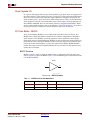
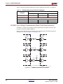
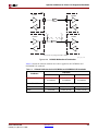
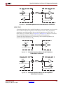
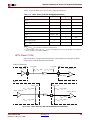
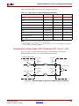
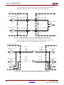
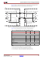
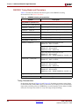
The following timing diagrams describe the behavior of the DCM clock outputs under four
different conditions.
1.
Reset/Lock
2.
Fixed-Phase Shifting
3.
Variable-Phase Shifting
4.
Status Flags
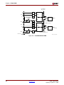
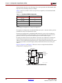
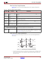
Reset/Lock
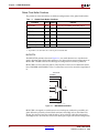
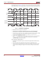
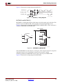
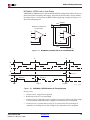
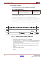
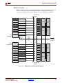
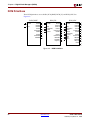
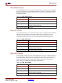
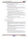
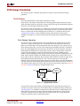
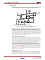
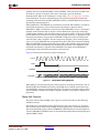
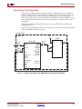
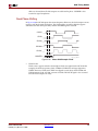
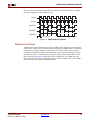
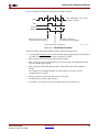
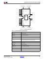
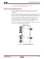
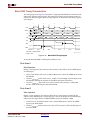
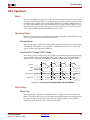
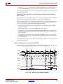
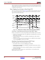
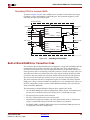
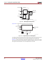
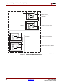
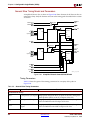
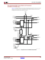
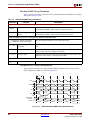
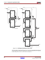
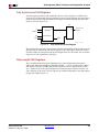
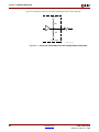
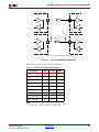
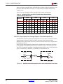
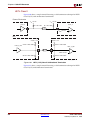
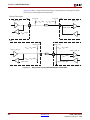
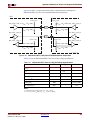
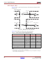
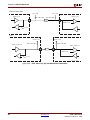
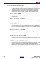
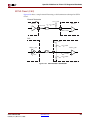
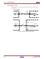
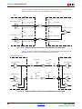
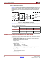
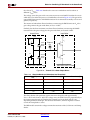
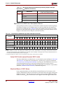
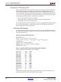
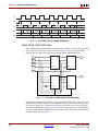
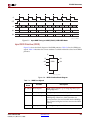
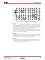
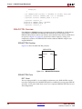
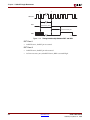
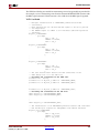
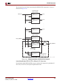
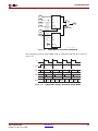
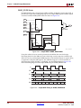
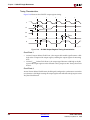
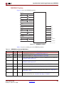
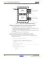
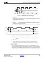
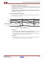
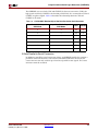
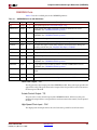
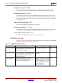
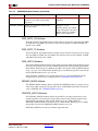
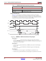
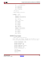
In Figure 2-19, the DCM is already locked. After the reset signal is applied, all output
clocks are stabilized to the desired values, and the LOCKED signal is asserted.
1
2
CLKIN
RST
3 Periods
CLK0
CLK90
CLK180
CLKFX
CLKFX180
CLKDV
LOCK
DLL
LOCKED
Figure 2-19:
•
ug070_2_19_083105
RESET/LOCK Example
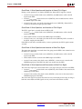
Prior to Clock Event 1
Prior to clock event 1, the DCM is locked. All clock outputs are in phase with the
correct frequency and behavior.
•
Clock Event 1
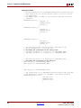
Some time after clock event 1 the reset signal is asserted at the (RST) pin. While reset is
asserted, all clock outputs become a logic zero. The reset signal is an asynchronous
reset. Note: the diagram is not shown to scale. For the DCM to operate properly, the
reset signal must be asserted for at least three CLKIN periods.
•
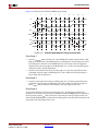
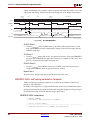
Clock Event 2
Clock event 2 occurs a few cycles after reset is asserted and deasserted. At clock event
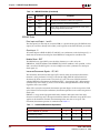
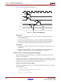
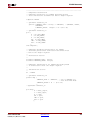
2, the lock process begins. At time LOCK_DLL, after clock event 2, if no fixed phase
88
www.xilinx.com
Virtex-4 User Guide
UG070 (v1.5) March 21, 2006