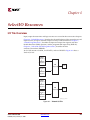
1
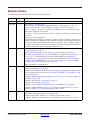
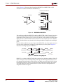
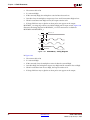
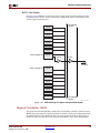
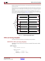
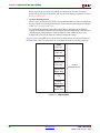
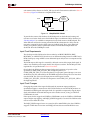
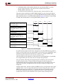
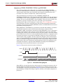
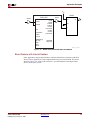
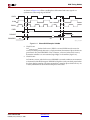
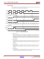
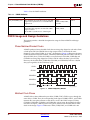
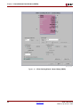
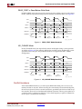
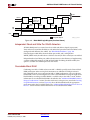
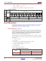
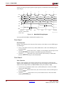
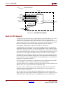
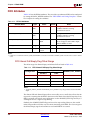
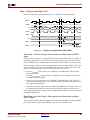
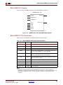
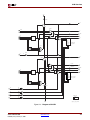
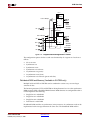
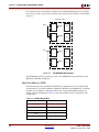
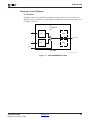
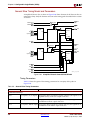
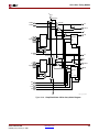
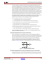
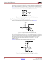
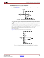
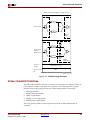
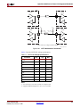
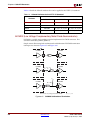
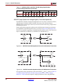
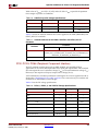
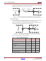
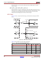
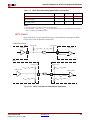
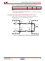
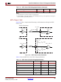
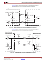
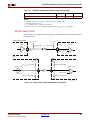
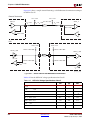
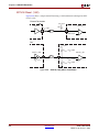
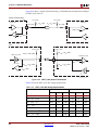
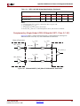
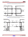
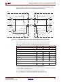
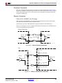
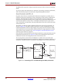
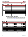
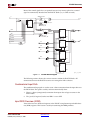
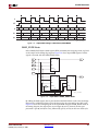
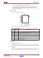
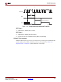
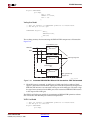
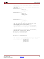
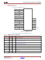
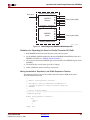
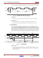
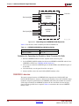
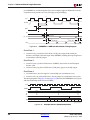
R
CLB / Slice Timing Models
Clock Event 1: Write Operation
During a Write operation, the contents of the memory at the address on the ADDR inputs
are changed. The data written to this memory location is reflected on the X/Y outputs
synchronously.
•
At time TWS before clock event 1, the write-enable signal (WE) becomes valid-high,
enabling the RAM for the following Write operation.
•
At time TAS before clock event 1, the address (2) becomes valid at the F/G inputs of
the RAM.
•
At time TDS or TCYCK before clock event 1, the DATA becomes valid (1) at the DI input
of the RAM and is reflected on the X/XMUX output at time TSHCKO after clock
event 1.
This is also applicable to the XMUX, YMUX, XB, YB, COUT, and F5 outputs at time TWOSCO,
TWOSX, TWOSXB, TWOSYB, and TSHCKOF5 after clock event 1.
Clock Event 2: Read Operation
All Read operations are asynchronous in distributed RAM. As long as WE is Low, the
address bus can be asserted at any time. The contents of the RAM on the address bus are
reflected on the X/Y outputs after a delay of length TILO (propagation delay through a
LUT). The address (F) is asserted after clock event 2, and the contents of the RAM at
address (F) are reflected on the output after a delay of length TILO.
Virtex-4 User Guide
UG070 (v2.0) January 4, 2007
www.xilinx.com
195