1
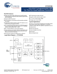
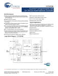
COMPUTE MODULE OPERATING INSTRUCTIONS POWERING THE MODULE The Compute Module has 6 separate supplies that must be present at all times (i.e. they must all be powered, you cannot leave any of them unpowered even if a specific interface or GPIO bank is unused). 1. VBAT is used to power the BCM2835 processor core (it feeds the SMPS that generates the chip core voltage) 2. 3V3 powers various BCM2835 PHYs, IO and the eMMC Flash 3. 1V8 powers various BCM2835 PHYs, IO and SDRAM 4. VDAC powers the composite (TV out) DAC 5. GPIO0-27_VREF powers the GPIO 0-27 IO bank 6. GPIO28-45_VREF powers the GPIO 28-45 IO bank SUPPLY VOLTAGE / VOLTAGE RANGE TOLERANCE 3V3 3.3V +/- 5% VBAT 2.3-5V [1] 1V8 1.8V GPIO0-27_VREF 1.8-3.3V VDAC GPIO28-45_VREF 2.5-2.8V (can connect to 3V3 if unused) 1.8-3.3V +/- 5% +/- 5% +/- 5% +/- 5% +/- 5% [1] **NOTE that the voltage range for best SMPS efficiency is ~3.3-4.3V POWER SEQUENCING upplies must be synchronised to come up at exactly the same time, or staggered such that the highest voltage comes up first, then the next S highest etc. This is to avoid forward biasing internal (on-chip) diodes between supplies and causing latch-up. POWER REQUIREMENTS xact power requirements will be heavily dependent upon the individual use case. If an on-chip subsystem is unused it is usually in a low E power state or completely turned off. For instance if your application does not use 3D graphics then a large part of the core digital logic will never turn on and need power. Similarly for camera / display interfaces, HDMI, USB interfaces, video encode/decode etc. owerchain design is critical for stable and reliable operation of the Compute Module. We strongly recommend that designers spend time P measuring and verifying power requirements for their particular use case and application, as well as paying careful attention to power supply sequencing and maximum supply voltage tolerance. he following table gives a rough guide as to minimum supply requirements. **However, the user is responsible for verifying that their powerT chain is designed sufficient for their application. In some more pathological use cases these minimum requirements may well be too low!** SUPPLY MINIMUM REQUIREMENT (MA OR MW) 3V3 250mA VBAT 1V8 VDAC GPIO0-27_VREF GPIO28-45_VREF 2000mW [1] 250mA 25mA See note [2] See note [2] [1] **NOTE VBAT is heavily dependent upon the application. E.g. with video encode, 3D and camera all running the power requirements can be substantial. [2] **NOTE that each GPIO bank will only need a few mW if unused, however when in use the requirements will vary depending on number of IOs in use, and the load on each. The designer is responsible for calculating or measuring this themselves based on their particular use case. MODULE BOOTING / FLASHING THE EMMC The 4GByte eMMC Flash device on the Compute module is directly connected to the primary BCM28235 SD/eMMC interface. These connections are not accessible on the module pins. hen initially powered on (or after the RUN pin has been held low and then released) the BCM2835 will try and access the eMMC W device and look for a file called bootcode.bin on the primary partition (which must be FAT) to start booting the system. If it cannot access the eMMC device or the boot code cannot be found, it will fall back to waiting for boot code to be written to it over USB (i.e. its USB port is in slave mode waiting to accept boot code from a suitable host). USB boot tool is available (https://github.com/raspberrypi/tools/tree/master/usbboot) which allows a host PC running Linux to write A the BCM2835 boot code over USB to the module. That boot code then runs and provides access to the eMMC as a USB mass storage device, which can then be read/written using the host PC. (Note that a Raspberry Pi can be used as the host machine). he compute module has a pin called EMMC_DISABLE_N which when shorted to GND will disable the eMMC, forcing BCM2835 to boot T from USB. Note that when the eMMC is disabled like this it takes a few seconds from power up for the processor to give up trying to talk to the eMMC device and fall back to booting from USB. **NOTE that once booted over USB, BCM2835 needs to re-enable the eMMC device (by releasing EMMC_DISABLE_N) to allow access to it as mass storage. It expects to be able to do this by driving the GPIO47_1V8 pin LOW (which at boot is initially an input with a pull up to 1V8). If an end user wishes to add the ability to access the eMMC over USB in their product, similar circuitry to that used on the Compute Module IO Board to enable/disable the USB boot and eMMC must be used (EMMC_DISABLE_N pulled low via MOSFET(s) and released again by MOSFET with gate controlled by GPIO47_1V8.) Be careful to use MOSFETs suitable for switching at 1.8V (i.e. use a device with Vt << 1.8V).** STEPS TO FLASH THE EMMC ON A COMPUTE MODULE USING A COMPUTE MODULE IO BOARD You need a host Linux system (a Raspberry Pi will do!). **ON YOUR COMPUTE MODULE IO BOARD:** Make sure that J4 (USB SLAVE BOOT ENABLE) is set to the ‘EN’ position. **ON YOUR HOST SYSTEM:** Git can get upset if the date is not set correctly so on a Raspberry Pi you can do a: sudo date MMDDhhmm Where MM is month, DD day and hh mm hours and minutes respectively. lone the usbboot tool repository and grab libusb: C sudo git clone --depth=1 https://github.com/raspberrypi/tools cd tools/usbboot sudo apt-get install libusb-1.0-0-dev uild the usbboot tool: B sudo make un the usbboot tool and it will wait for a connection: R sudo ./rpiboot Now plug the host machine into Compute Module IO Board USB slave port (J15) and power on the CMIO board. The usbboot tool will see the compute module and send it boot code to allow access to the eMMC. Once complete you will see a new device appear, commonly /dev/sda (but it could be /dev/sdb etc. so have a look in /dev/ before running rpiboot so you can see what changes). ou now need to write a raw OS image (e.g. [Raspian](http://downloads.raspberrypi.org/raspbian_latest) to the device. Y Note the following command may take some time to complete (depends on the size of the image): sudo dd if=raw_os_image_of_your_choice.img of=/dev/sda bs=4MiB nce the image has been written, unplug and re-plug the USB, and you should see 2 partitions appear (for Raspian) in /dev O In total you should see something like: /dev/sda Device /dev/sda1 First partition (FAT) /dev/sda2 Second partition (Linux filesystem) The /dev/sda1 and /dev/sda2 partitions can now be mounted normally. Make sure J4 (USB SLAVE BOOT ENABLE) is set to the disabled position and/or nothing is plugged into the USB slave port. Power cycling the IO board should now result in the Compute Module booting from eMMC. COMPUTE MODULE INTERFACES GPIOs **NOTE that the GPIO46_1V8 and GPIO47_1V8 pins are 1.8V IO only and are reserved for special functions (HDMI hot plug detect and boot control respectively). Please don't use these pins for any other purpose (as the software for the Compute Module will always expect these pins to have these special functions). If unused please leave unconnected. The remaining GPIOs are available for general use and are split into 2 banks. GPIO0 to GPIO27 are bank 0 and GPIO28-45 make up bank 1. GPIO0-27_VREF is the power supply for bank 0 and GPIO28-45_VREF is the power supply for bank 1. These supplies can be in the range 1.8V-3.3V. These supplies are not optional; each bank must be powered (even when none of the GPIOs for that bank are used). All GPIOs except GPIO28, 29, 44 and 45 have weak in-pad pull-ups or pull-downs enabled from power on. Whether the GPIO is pulled up or down is documented in the BCM2835 peripherals document section 6.2. **It is recommended to add off-chip pulls to GPIO28, 29, 44 and 45 to make sure they never float during power on / initial boot.** CSI (MIPI Serial Camera) The Compute Module has 2 MIPI serial camera interfaces (CSI), Interface 0 and Interface 1. Interface 0 is a 2-lane interface (one clock lane and 2 data lanes). Interface 1 is a 4-lane interface (one clock lane and 4 data lanes). Note that the Raspberry Pi Model A/B camera connector uses Interface 1 (but only in a 2-lane configuration). The camera interface(s) clock and data pins must be routed as matched length, matched phase 100 ohm differential PCB traces. DSI (MIPI Serial Display) The Compute Module has 2 MIPI serial display interfaces (DSI), Interface 0 and Interface 1. Interface 0 is a 2-lane interface (one clock lane and 2 data lanes). Interface 1 is a 4-lane interface (one clock lane and 4 data lanes). Note that the Raspberry Pi Model A/B display connector uses Interface 1 (but only in a 2-lane configuration). The display interface(s) clock and data pins must be routed as matched length, matched phase 100 ohm differential PCB traces. USB OTG The BCM2835 USB port is On-The-Go (OTG) capable. If using either as a fixed slave or fixed master please tie the USB_OTGID pin to ground. The USB port (Pins USB_DP and USB_DM) must be routed as matched-phase 90 ohm differential PCB traces. Note that the port is capable of being used as a true OTG port but currently there is no documentation / code / examples for this use case. HDMI It is recommended to follow a similar arrangement to the Compute Module IO Board circuitry for HDMI output. The HDMI CK_P/N (clock) and D0-D3_P/N (data) pins must each be routed as matched length 100 ohm differential PCB traces. It is also important to make sure that each differential pair is closely phase matched. Finally, keep HDMI traces well away from other noise sources, and as short as possible. **FAILURE TO OBSERVE THESE DESIGN RULES IS LIKELY TO RESULT IN EMC FAILURE.** COMPOSITE (TVDAC) The TVDAC pin can be used to output composite video. Please route this signal away from noise sources and using a 75 ohm PCB trace. If the TVDAC output is not used, VDAC can be connected to 3V3 but it must be powered even if the TV out functionality is unused. **NOTE that the TV DAC is powered from the VDAC supply which must be a clean supply of 2.5-2.8V (it is recommended to generate this supply from 3V3 using a low noise LDO). COMPUTE MODULE TEMPERATURE RANGE The operating temperature range of the module is set by the lowest maximum of any of the components, and the highest minimum of any of the components. The Samsung eMMC and Samsung LPDDR2 are all rated for -25 to +80 degrees C, so the range is -25 to +80. (BCM2835 and the analogue switch have a greater range; the ceramic capacitors are specified from -25 to +85). However that is the max range for the silicon die, so a user would have to take into account the heat generated when in use and make sure this does not cause the temperature to exceed 80C. **THE USER IS RESPONSIBLE FOR DESIGNING AND TESTING THEIR SYSTEM SUCH THAT THESE LIMITS ARE NOT EXCEEDED.** COMPUTE MODULE FORM FACTOR The Compute Module conforms to JEDEC MO-224 mechanical specification for 200 pin DDR2 (1.8V) SODIMM modules. (Please note that the pinout of the Compute Module is not the same as a DDR2 SODIMM module, they are **not** electrically compatible). The maximum component height on the underside of the Compute Module is 1.2mm The maximum component height on the top side of the Compute Module is 1.5mm The Compute Module PCB thickness is 1.0mm +/- 10%* **NOTE that the location and arrangement of components on the Compute Module may change slightly over time due to revisions for cost and manufacturability; however maximum component heights and PCB thickness will be kept as specified. Raspberry Pi Documentation by the Raspberry Pi Foundation is licensed under a Creative Commons Attribution 4.0 International Licence. Based on a work at https://github.com/raspberrypi/documentation. COMPLIANT WITH www.element14.com/legistration www.raspberrypi.org Premier Farnell UK, 150 Armley Road, Leeds, LS12 2QQ, United Kingdom