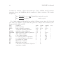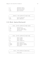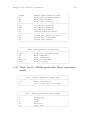
1
NGSPICE User Manual Describes ngspice-rework-17 Draft Version 0.2 Many Authors Copyright 1996 The Regents of the University of California. Permission to use, copy, modify, and distribute this software and its documentation for educational, research and non-profit purposes, without fee, and without a written agreement is hereby granted, provided that the above copyright notice, this paragraph and the following three paragraphs appear in all copies. This software program and documentation are copyrighted by The Regents of the University of California. The software program and documentation are supplied "as is", without any accompanying services from The Regents. The Regents does not warrant that the operation of the program will be uninterrupted or error-free. The end-user understands that the program was developed for research purposes and is advised not to rely exclusively on the program for any reason. IN NO EVENT SHALL THE UNIVERSITY OF CALIFORNIA BE LIABLE TO ANY PARTY FOR DIRECT, INDIRECT, SPECIAL, INCIDENTAL, OR CONSEQUENTIAL DAMAGES, INCLUDING LOST PROFITS, ARISING OUT OF THE USE OF THIS SOFTWARE AND ITS DOCUMENTATION, EVEN IF THE UNIVERSITY OF CALIFORNIA HAS BEEN ADVISED OF THE POSSIBILITY OF SUCH DAMAGE. THE UNIVERSITY OF CALIFORNIA SPECIFICALLY DISCLAIMS ANY WARRANTIES, INCLUDING, BUT NOT LIMITED TO, THE IMPLIED WARRANTIES OF MERCHANTABILITY AND FITNESS FOR A PARTICULAR PURPOSE. THE SOFTWARE PROVIDED HEREUNDER IS ON AN "AS IS" BASIS, AND THE UNIVERSITY OF CALIFORNIA HAS NO OBLIGATIONS TO PROVIDE MAINTENANCE, SUPPORT, UPDATES, ENHANCEMENTS, OR MODIFICATIONS. i Table of Contents 1 Preface. . . . . . . . . . . . . . . . . . . . . . . . . . . . . . . . . . . . 1 2 Acknowledgements . . . . . . . . . . . . . . . . . . . . . . . . . 3 3 Release Notes . . . . . . . . . . . . . . . . . . . . . . . . . . . . . 5 3.1 Reporting a bug . . . . . . . . . . . . . . . . . . . . . . . . . . . . . . . . . . . . . . . . . . . . 11 4 Introduction . . . . . . . . . . . . . . . . . . . . . . . . . . . . . . 13 5 NGSPICE Compilation . . . . . . . . . . . . . . . . . . . 15 5.1 5.2 5.3 5.4 5.5 6 Extracting the archive . . . . . . . . . . . . . . . . . . . . . . . . . . . . . . . . . . . . . . Configuring NGSPICE . . . . . . . . . . . . . . . . . . . . . . . . . . . . . . . . . . . . . . Compiling NGSPICE . . . . . . . . . . . . . . . . . . . . . . . . . . . . . . . . . . . . . . . Supported systems . . . . . . . . . . . . . . . . . . . . . . . . . . . . . . . . . . . . . . . . . Platform specific issues . . . . . . . . . . . . . . . . . . . . . . . . . . . . . . . . . . . . . Supported Analyses . . . . . . . . . . . . . . . . . . . . . . . 19 6.1 Types of Analysis . . . . . . . . . . . . . . . . . . . . . . . . . . . . . . . . . . . . . . . . . . 6.1.1 DC Analysis. . . . . . . . . . . . . . . . . . . . . . . . . . . . . . . . . . . . . . . . . . . 6.1.2 AC Small-Signal Analysis . . . . . . . . . . . . . . . . . . . . . . . . . . . . . . 6.1.3 Transient Analysis . . . . . . . . . . . . . . . . . . . . . . . . . . . . . . . . . . . . . 6.1.4 Pole-Zero Analysis . . . . . . . . . . . . . . . . . . . . . . . . . . . . . . . . . . . . . 6.1.5 Small-Signal Distortion Analysis . . . . . . . . . . . . . . . . . . . . . . . . 6.1.6 Sensitivity Analysis . . . . . . . . . . . . . . . . . . . . . . . . . . . . . . . . . . . . 6.1.7 Noise Analysis . . . . . . . . . . . . . . . . . . . . . . . . . . . . . . . . . . . . . . . . . 6.2 Analysis at Different Temperatures . . . . . . . . . . . . . . . . . . . . . . . . . . 6.3 Convergence . . . . . . . . . . . . . . . . . . . . . . . . . . . . . . . . . . . . . . . . . . . . . . . 7 15 15 17 17 18 19 19 19 19 19 20 20 20 21 22 Circuit Description . . . . . . . . . . . . . . . . . . . . . . . 23 7.1 7.2 General Structure and Conventions . . . . . . . . . . . . . . . . . . . . . . . . . . Basics: Title Line, Comment Lines and .END Line . . . . . . . . . . . . 7.2.1 Title Line . . . . . . . . . . . . . . . . . . . . . . . . . . . . . . . . . . . . . . . . . . . . . 7.2.2 .END Line . . . . . . . . . . . . . . . . . . . . . . . . . . . . . . . . . . . . . . . . . . . . 7.2.3 Comments . . . . . . . . . . . . . . . . . . . . . . . . . . . . . . . . . . . . . . . . . . . . 7.3 Device Models . . . . . . . . . . . . . . . . . . . . . . . . . . . . . . . . . . . . . . . . . . . . . 7.4 Subcircuits . . . . . . . . . . . . . . . . . . . . . . . . . . . . . . . . . . . . . . . . . . . . . . . . 7.4.1 .SUBCKT Line . . . . . . . . . . . . . . . . . . . . . . . . . . . . . . . . . . . . . . . . 7.4.2 ENDS Line . . . . . . . . . . . . . . . . . . . . . . . . . . . . . . . . . . . . . . . . . . . . 7.4.3 Subcircuit Calls . . . . . . . . . . . . . . . . . . . . . . . . . . . . . . . . . . . . . . . 7.5 INCLUDE . . . . . . . . . . . . . . . . . . . . . . . . . . . . . . . . . . . . . . . . . . . . . . . . . 23 24 24 24 24 24 26 26 26 27 27 ii 8 NGSPICE User Manual Circuit Elements and Models . . . . . . . . . . . . . . 29 8.1 General options and information. . . . . . . . . . . . . . . . . . . . . . . . . . . . . 8.1.1 Simulating more devices in parallel . . . . . . . . . . . . . . . . . . . . . . 8.1.2 Technology scaling . . . . . . . . . . . . . . . . . . . . . . . . . . . . . . . . . . . . . 8.1.3 Model binning . . . . . . . . . . . . . . . . . . . . . . . . . . . . . . . . . . . . . . . . . 8.2 Elementary Devices . . . . . . . . . . . . . . . . . . . . . . . . . . . . . . . . . . . . . . . . 8.2.1 Resistors . . . . . . . . . . . . . . . . . . . . . . . . . . . . . . . . . . . . . . . . . . . . . . 8.2.2 Semiconductor Resistors. . . . . . . . . . . . . . . . . . . . . . . . . . . . . . . . 8.2.3 Semiconductor Resistor Model (R) . . . . . . . . . . . . . . . . . . . . . . 8.2.4 Capacitors . . . . . . . . . . . . . . . . . . . . . . . . . . . . . . . . . . . . . . . . . . . . 8.2.5 Semiconductor Capacitors . . . . . . . . . . . . . . . . . . . . . . . . . . . . . . 8.2.6 Semiconductor Capacitor Model (C) . . . . . . . . . . . . . . . . . . . . 8.2.7 Inductors . . . . . . . . . . . . . . . . . . . . . . . . . . . . . . . . . . . . . . . . . . . . . 8.2.8 Inductor model . . . . . . . . . . . . . . . . . . . . . . . . . . . . . . . . . . . . . . . . 8.2.9 Coupled (Mutual) Inductors . . . . . . . . . . . . . . . . . . . . . . . . . . . . 8.2.10 Switches . . . . . . . . . . . . . . . . . . . . . . . . . . . . . . . . . . . . . . . . . . . . . 8.2.11 Switch Model (SW/CSW) . . . . . . . . . . . . . . . . . . . . . . . . . . . . . 8.3 Voltage and Current Sources . . . . . . . . . . . . . . . . . . . . . . . . . . . . . . . . 8.3.1 Independent Sources . . . . . . . . . . . . . . . . . . . . . . . . . . . . . . . . . . . 8.3.1.1 Pulse . . . . . . . . . . . . . . . . . . . . . . . . . . . . . . . . . . . . . . . . . . . . . 8.3.1.2 Sinusoidal . . . . . . . . . . . . . . . . . . . . . . . . . . . . . . . . . . . . . . . . 8.3.1.3 Exponential. . . . . . . . . . . . . . . . . . . . . . . . . . . . . . . . . . . . . . . 8.3.1.4 Piece-Wise Linear . . . . . . . . . . . . . . . . . . . . . . . . . . . . . . . . . 8.3.1.5 Single-Frequency FM . . . . . . . . . . . . . . . . . . . . . . . . . . . . . . 8.3.2 Linear Dependent Sources . . . . . . . . . . . . . . . . . . . . . . . . . . . . . . 8.3.2.1 Linear Voltage-Controlled Current Sources . . . . . . . . . . 8.3.2.2 Linear Voltage-Controlled Voltage Sources . . . . . . . . . . 8.3.2.3 Linear Current-Controlled Current Sources . . . . . . . . . . 8.3.2.4 Linear Current-Controlled Voltage Sources . . . . . . . . . . 8.3.3 Non-linear Dependent Sources . . . . . . . . . . . . . . . . . . . . . . . . . . 8.4 Transmission Lines . . . . . . . . . . . . . . . . . . . . . . . . . . . . . . . . . . . . . . . . . 8.4.1 Lossless Transmission Lines . . . . . . . . . . . . . . . . . . . . . . . . . . . . . 8.4.2 Lossy Transmission Lines . . . . . . . . . . . . . . . . . . . . . . . . . . . . . . . 8.4.3 Lossy Transmission Line Model (LTRA) . . . . . . . . . . . . . . . . . 8.4.4 Uniform Distributed RC Lines (Lossy) . . . . . . . . . . . . . . . . . . 8.4.5 Uniform Distributed RC Model (URC) . . . . . . . . . . . . . . . . . . 8.5 Transistors and Diodes . . . . . . . . . . . . . . . . . . . . . . . . . . . . . . . . . . . . . 8.5.1 Junction Diodes . . . . . . . . . . . . . . . . . . . . . . . . . . . . . . . . . . . . . . . 8.5.2 Diode Model (D) . . . . . . . . . . . . . . . . . . . . . . . . . . . . . . . . . . . . . . 8.5.3 Diode Equations . . . . . . . . . . . . . . . . . . . . . . . . . . . . . . . . . . . . . . . 8.5.4 Bipolar Junction Transistors (BJTs) . . . . . . . . . . . . . . . . . . . . 8.5.5 BJT Models (NPN/PNP) . . . . . . . . . . . . . . . . . . . . . . . . . . . . . . 8.5.6 Junction Field-Effect Transistors (JFETs) . . . . . . . . . . . . . . . 8.5.7 JFET Models (NJF/PJF) . . . . . . . . . . . . . . . . . . . . . . . . . . . . . . 8.5.8 MOSFETs . . . . . . . . . . . . . . . . . . . . . . . . . . . . . . . . . . . . . . . . . . . . 8.5.9 MOSFET Models (NMOS/PMOS) . . . . . . . . . . . . . . . . . . . . . . 8.5.10 MESFETs . . . . . . . . . . . . . . . . . . . . . . . . . . . . . . . . . . . . . . . . . . . 8.5.11 MESFET Models (NMF/PMF) . . . . . . . . . . . . . . . . . . . . . . . . 29 29 29 29 30 30 31 31 32 33 33 35 35 36 37 37 38 38 39 39 39 40 40 41 41 41 41 41 42 43 43 43 44 45 46 46 47 47 48 52 52 55 55 56 57 61 61 iii 9 Analyses and Output Control. . . . . . . . . . . . . . 63 9.1 9.2 Simulator Variables (.OPTIONS) . . . . . . . . . . . . . . . . . . . . . . . . . . . . Initial Conditions . . . . . . . . . . . . . . . . . . . . . . . . . . . . . . . . . . . . . . . . . . 9.2.1 .NODESET: Specify Initial Node Voltage Guesses . . . . . . . . 9.2.2 .IC: Set Initial Conditions . . . . . . . . . . . . . . . . . . . . . . . . . . . . . . 9.3 Analyses . . . . . . . . . . . . . . . . . . . . . . . . . . . . . . . . . . . . . . . . . . . . . . . . . . . 9.3.1 .AC: Small-Signal AC Analysis . . . . . . . . . . . . . . . . . . . . . . . . . 9.3.2 .DC: DC Transfer Function . . . . . . . . . . . . . . . . . . . . . . . . . . . . . 9.3.3 .DISTO: Distortion Analysis . . . . . . . . . . . . . . . . . . . . . . . . . . . . 9.3.4 .NOISE: Noise Analysis . . . . . . . . . . . . . . . . . . . . . . . . . . . . . . . . 9.3.5 .OP: Operating Point Analysis . . . . . . . . . . . . . . . . . . . . . . . . . . 9.3.6 .PZ: Pole-Zero Analysis . . . . . . . . . . . . . . . . . . . . . . . . . . . . . . . . 9.3.7 .SENS: DC or Small-Signal AC Sensitivity Analysis . . . . . . 9.3.8 .TF: Transfer Function Analysis . . . . . . . . . . . . . . . . . . . . . . . . 9.3.9 .TRAN: Transient Analysis . . . . . . . . . . . . . . . . . . . . . . . . . . . . . 9.4 Batch Output . . . . . . . . . . . . . . . . . . . . . . . . . . . . . . . . . . . . . . . . . . . . . . 9.4.1 .SAVE Lines . . . . . . . . . . . . . . . . . . . . . . . . . . . . . . . . . . . . . . . . . . 9.4.2 .PRINT Lines . . . . . . . . . . . . . . . . . . . . . . . . . . . . . . . . . . . . . . . . . 9.4.3 .PLOT Lines . . . . . . . . . . . . . . . . . . . . . . . . . . . . . . . . . . . . . . . . . . 9.4.4 .FOUR: Fourier Analysis of Transient Analysis Output . . . 10 63 65 65 66 66 66 67 67 69 69 69 70 70 71 71 71 71 72 73 Interactive Interpreter . . . . . . . . . . . . . . . . . . . 75 10.1 Expressions, Functions, and Constants . . . . . . . . . . . . . . . . . . . . . . 10.2 Command Interpretation. . . . . . . . . . . . . . . . . . . . . . . . . . . . . . . . . . . 10.3 Commands . . . . . . . . . . . . . . . . . . . . . . . . . . . . . . . . . . . . . . . . . . . . . . . 10.3.1 Ac*: Perform an AC, small-signal frequency response analysis . . . . . . . . . . . . . . . . . . . . . . . . . . . . . . . . . . . . . . . . . . . . . . . . . 10.3.2 Alias: Create an alias for a command . . . . . . . . . . . . . . . . . . 10.3.3 Alter*: Change a device or model parameter . . . . . . . . . . . . 10.3.4 Asciiplot: Plot values using old-style character plots . . . . . 10.3.5 Aspice: Asynchronous ngspice run . . . . . . . . . . . . . . . . . . . . . 10.3.6 Bug: Mail a bug report . . . . . . . . . . . . . . . . . . . . . . . . . . . . . . . 10.3.7 Cd: Change directory . . . . . . . . . . . . . . . . . . . . . . . . . . . . . . . . . 10.3.8 Destroy: Delete a data set . . . . . . . . . . . . . . . . . . . . . . . . . . . . . 10.3.9 Dc*: Perform a DC-sweep analysis . . . . . . . . . . . . . . . . . . . . . 10.3.10 Define: Define a function . . . . . . . . . . . . . . . . . . . . . . . . . . . . . 10.3.11 Delete*: Remove a trace or breakpoint . . . . . . . . . . . . . . . . 10.3.12 Diff: Compare vectors . . . . . . . . . . . . . . . . . . . . . . . . . . . . . . . . 10.3.13 Display: List known vectors and types . . . . . . . . . . . . . . . . 10.3.14 Echo: Print text . . . . . . . . . . . . . . . . . . . . . . . . . . . . . . . . . . . . . 10.3.15 Edit*: Edit the current circuit . . . . . . . . . . . . . . . . . . . . . . . . 10.3.16 Fourier: Perform a fourier transform . . . . . . . . . . . . . . . . . . 10.3.17 Hardcopy: Save a plot to a file for printing . . . . . . . . . . . . 10.3.18 Help: Print summaries of Ngspice commands . . . . . . . . . . 10.3.19 History: Review previous commands . . . . . . . . . . . . . . . . . . 10.3.20 Iplot*: Incremental plot . . . . . . . . . . . . . . . . . . . . . . . . . . . . . . 10.3.21 Jobs: List active asynchronous ngspice runs. . . . . . . . . . . . 10.3.22 Let: Assign a value to a vector . . . . . . . . . . . . . . . . . . . . . . . 76 79 80 80 80 80 80 80 81 81 81 81 81 81 82 82 82 82 82 83 83 83 83 83 83 iv NGSPICE User Manual 10.3.23 Linearize*: Interpolate to a linear scale . . . . . . . . . . . . . . . . 84 10.3.24 Listing*: Print a listing of the current circuit . . . . . . . . . . 84 10.3.25 Load: Load rawfile data . . . . . . . . . . . . . . . . . . . . . . . . . . . . . . 84 10.3.26 Op*: Perform an operating point analysis . . . . . . . . . . . . . 84 10.3.27 Plot: Plot values on the display . . . . . . . . . . . . . . . . . . . . . . . 84 10.3.28 Print: Print values . . . . . . . . . . . . . . . . . . . . . . . . . . . . . . . . . . . 85 10.3.29 Quit: Leave Ngspice or Nutmeg . . . . . . . . . . . . . . . . . . . . . . . 85 10.3.30 Rehash: Reset internal hash tables . . . . . . . . . . . . . . . . . . . . 85 10.3.31 Reset*: Reset an analysis . . . . . . . . . . . . . . . . . . . . . . . . . . . . 85 10.3.32 Reshape: Alter the dimensionality or dimensions of . . . . 86 10.3.33 Resume*: Continue a simulation after a stop. . . . . . . . . . . 86 10.3.34 Rspice: Remote ngspice submission . . . . . . . . . . . . . . . . . . . 86 10.3.35 Run*: Run analysis from the input file . . . . . . . . . . . . . . . . 86 10.3.36 Rusage: Resource usage . . . . . . . . . . . . . . . . . . . . . . . . . . . . . . 87 10.3.37 Save*: Save a set of outputs . . . . . . . . . . . . . . . . . . . . . . . . . . 87 10.3.38 Sens*: Run a sensitivity analysis . . . . . . . . . . . . . . . . . . . . . . 87 10.3.39 Set: Set the value of a variable . . . . . . . . . . . . . . . . . . . . . . . 88 10.3.40 Setcirc*: Change the current circuit . . . . . . . . . . . . . . . . . . . 88 10.3.41 Setplot: Switch the current set of vectors . . . . . . . . . . . . . . 88 10.3.42 Settype: Set the type of a vector . . . . . . . . . . . . . . . . . . . . . . 88 10.3.43 Shell: Call the command interpreter. . . . . . . . . . . . . . . . . . . 88 10.3.44 Shift: Alter a list variable . . . . . . . . . . . . . . . . . . . . . . . . . . . . 89 10.3.45 Show*: List device state . . . . . . . . . . . . . . . . . . . . . . . . . . . . . 89 10.3.46 Showmod*: List model parameter values . . . . . . . . . . . . . . 89 10.3.47 Source: Read a Ngspice input file . . . . . . . . . . . . . . . . . . . . . 89 10.3.48 Status*: Display breakpoint information . . . . . . . . . . . . . . . 90 10.3.49 Step*: Run a fixed number of timepoints . . . . . . . . . . . . . . 90 10.3.50 Stop*: Set a breakpoint . . . . . . . . . . . . . . . . . . . . . . . . . . . . . . 90 10.3.51 Sysinfo: Print system information . . . . . . . . . . . . . . . . . . . . . 90 10.3.52 Tf*: Run a Transfer Function analysis . . . . . . . . . . . . . . . . 91 10.3.53 Trace*: Trace nodes . . . . . . . . . . . . . . . . . . . . . . . . . . . . . . . . . 91 10.3.54 Tran*: Perform a transient analysis . . . . . . . . . . . . . . . . . . . 91 10.3.55 Transpose: Swap the elements in a multi-dimensional data set . . . . . . . . . . . . . . . . . . . . . . . . . . . . . . . . . . . . . . . . . . . . . . . . . . . . . . 91 10.3.56 Unalias: Retract an alias . . . . . . . . . . . . . . . . . . . . . . . . . . . . . 92 10.3.57 Undefine: Retract a definition . . . . . . . . . . . . . . . . . . . . . . . . 92 10.3.58 Unset: Clear a variable. . . . . . . . . . . . . . . . . . . . . . . . . . . . . . . 92 10.3.59 Version: Print the version of ngspice . . . . . . . . . . . . . . . . . . 92 10.3.60 Where: Identify troublesome node or device . . . . . . . . . . . 93 10.3.61 Write: Write data to a file . . . . . . . . . . . . . . . . . . . . . . . . . . . . 93 10.3.62 Xgraph: use the xgraph(1) program for plotting. . . . . . . . 93 10.4 Control Structures . . . . . . . . . . . . . . . . . . . . . . . . . . . . . . . . . . . . . . . . 93 10.4.1 While - End . . . . . . . . . . . . . . . . . . . . . . . . . . . . . . . . . . . . . . . . . . 93 10.4.2 Repeat - End . . . . . . . . . . . . . . . . . . . . . . . . . . . . . . . . . . . . . . . . . 94 10.4.3 Dowhile - End . . . . . . . . . . . . . . . . . . . . . . . . . . . . . . . . . . . . . . . . 94 10.4.4 Foreach - End . . . . . . . . . . . . . . . . . . . . . . . . . . . . . . . . . . . . . . . . 94 10.4.5 If - Then - Else . . . . . . . . . . . . . . . . . . . . . . . . . . . . . . . . . . . . . . . 94 10.4.6 Label . . . . . . . . . . . . . . . . . . . . . . . . . . . . . . . . . . . . . . . . . . . . . . . . 95 v 10.4.7 Goto. . . . . . . . . . . . . . . . . . . . . . . . . . . . . . . . . . . . . . . . . . . . . . . . . 95 10.4.8 Continue . . . . . . . . . . . . . . . . . . . . . . . . . . . . . . . . . . . . . . . . . . . . . 95 10.4.9 Break . . . . . . . . . . . . . . . . . . . . . . . . . . . . . . . . . . . . . . . . . . . . . . . . 95 10.5 Variables . . . . . . . . . . . . . . . . . . . . . . . . . . . . . . . . . . . . . . . . . . . . . . . . . 95 10.6 MISCELLANEOUS . . . . . . . . . . . . . . . . . . . . . . . . . . . . . . . . . . . . . . 100 10.7 Bugs . . . . . . . . . . . . . . . . . . . . . . . . . . . . . . . . . . . . . . . . . . . . . . . . . . . . 101 11 Bibliography . . . . . . . . . . . . . . . . . . . . . . . . . . . 103 12 Example Circuits . . . . . . . . . . . . . . . . . . . . . . . 105 12.1 12.2 12.3 12.4 12.5 13 Differential Pair . . . . . . . . . . . . . . . . . . . . . . . . . . . . . . . . . . . . . . . . . . MOSFET Characterization . . . . . . . . . . . . . . . . . . . . . . . . . . . . . . . RTL Inverter . . . . . . . . . . . . . . . . . . . . . . . . . . . . . . . . . . . . . . . . . . . . Four-Bit Binary Adder . . . . . . . . . . . . . . . . . . . . . . . . . . . . . . . . . . . Transmission-Line Inverter . . . . . . . . . . . . . . . . . . . . . . . . . . . . . . . . 105 105 105 106 107 Model and Device Parameters . . . . . . . . . . . 109 13.1 URC: Uniform R.C. line . . . . . . . . . . . . . . . . . . . . . . . . . . . . . . . . . . 13.2 ASRC: Arbitrary Source . . . . . . . . . . . . . . . . . . . . . . . . . . . . . . . . . . 13.3 BJT: Bipolar Junction Transistor. . . . . . . . . . . . . . . . . . . . . . . . . . 13.4 BSIM1: Berkeley Short Channel IGFET Model . . . . . . . . . . . . . 13.5 BSIM2: Berkeley Short Channel IGFET Model . . . . . . . . . . . . . 13.6 Capacitor: Fixed capacitor . . . . . . . . . . . . . . . . . . . . . . . . . . . . . . . . 13.7 CCCS: Current controlled current source . . . . . . . . . . . . . . . . . . . 13.8 CCVS: Linear current controlled current source . . . . . . . . . . . . . 13.9 CSwitch: Current controlled ideal switch . . . . . . . . . . . . . . . . . . . 13.10 Diode: Junction Diode model . . . . . . . . . . . . . . . . . . . . . . . . . . . . 13.11 Inductor: Inductors . . . . . . . . . . . . . . . . . . . . . . . . . . . . . . . . . . . . . 13.12 mutual: Mutual inductors . . . . . . . . . . . . . . . . . . . . . . . . . . . . . . . 13.13 Isource: Independent current source . . . . . . . . . . . . . . . . . . . . . . 13.14 JFET: Junction Field effect transistor . . . . . . . . . . . . . . . . . . . . 13.15 LTRA: Lossy transmission line . . . . . . . . . . . . . . . . . . . . . . . . . . . 13.16 MES: GaAs MESFET model . . . . . . . . . . . . . . . . . . . . . . . . . . . . . 13.17 Mos1: Level 1 MOSfet model with Meyer capacitance model .......................................................... 13.18 Mos2: Level 2 MOSfet model with Meyer capacitance model .......................................................... 13.19 Mos3: Level 3 MOSfet model with Meyer capacitance model .......................................................... 13.20 Mos6: Level 6 MOSfet model with Meyer capacitance model .......................................................... 13.21 Resistor: Simple linear resistor . . . . . . . . . . . . . . . . . . . . . . . . . . . 13.22 Switch: Ideal voltage controlled switch . . . . . . . . . . . . . . . . . . . . 13.23 Tranline: Lossless transmission line . . . . . . . . . . . . . . . . . . . . . . . 13.24 VCCS: Voltage controlled current source . . . . . . . . . . . . . . . . . . 13.25 VCVS: Voltage controlled voltage source . . . . . . . . . . . . . . . . . . 13.26 Vsource: Independent voltage source . . . . . . . . . . . . . . . . . . . . . 109 110 110 114 117 122 123 123 124 125 126 127 127 128 130 131 133 137 140 144 148 149 150 151 151 152 vi NGSPICE User Manual 14 NGSPICE enhancements over Spice3 . . . . 155 14.1 Device models code . . . . . . . . . . . . . . . . . . . . . . . . . . . . . . . . . . . . . . 14.1.1 Resistor Model . . . . . . . . . . . . . . . . . . . . . . . . . . . . . . . . . . . . . . 14.1.2 Capacitor Model. . . . . . . . . . . . . . . . . . . . . . . . . . . . . . . . . . . . . 14.1.3 Diode (D) model fixes . . . . . . . . . . . . . . . . . . . . . . . . . . . . . . . . 14.1.4 Level 1 MOS model . . . . . . . . . . . . . . . . . . . . . . . . . . . . . . . . . . 14.1.5 Level 2 MOS Model. . . . . . . . . . . . . . . . . . . . . . . . . . . . . . . . . . 14.1.6 Level 3 Mos Model . . . . . . . . . . . . . . . . . . . . . . . . . . . . . . . . . . 14.1.7 switch model . . . . . . . . . . . . . . . . . . . . . . . . . . . . . . . . . . . . . . . . 14.1.8 current switch model . . . . . . . . . . . . . . . . . . . . . . . . . . . . . . . . . 14.1.9 boh . . . . . . . . . . . . . . . . . . . . . . . . . . . . . . . . . . . . . . . . . . . . . . . . . 14.1.10 PN diode voltage limiting . . . . . . . . . . . . . . . . . . . . . . . . . . . 14.1.11 FET voltage limiting. . . . . . . . . . . . . . . . . . . . . . . . . . . . . . . . 14.1.12 Meyer model improvement . . . . . . . . . . . . . . . . . . . . . . . . . . 15 The BSIM3 Model Integration . . . . . . . . . . 183 15.1 BSIM3 Revisions . . . . . . . . . . . . . . . . . . . . . . . . . . . . . . . . . . . . . . . . . 15.2 The integration process . . . . . . . . . . . . . . . . . . . . . . . . . . . . . . . . . . . 15.3 The multirevision code . . . . . . . . . . . . . . . . . . . . . . . . . . . . . . . . . . . 15.4 Device Multiplicity . . . . . . . . . . . . . . . . . . . . . . . . . . . . . . . . . . . . . . . 15.4.1 Adding the "m" parameter . . . . . . . . . . . . . . . . . . . . . . . . . . . 15.5 BSIM3 TNOM patch . . . . . . . . . . . . . . . . . . . . . . . . . . . . . . . . . . . . . 15.6 References for BSIM3 model . . . . . . . . . . . . . . . . . . . . . . . . . . . . . . 16 155 155 155 156 156 159 165 181 181 181 181 181 182 183 183 184 186 187 190 190 EKV Model . . . . . . . . . . . . . . . . . . . . . . . . . . . . 193 Chapter 1: Preface 1 1 Preface The NGSPICE user’s manual is based on the text file included in the Spice3f source package. The original text has been converted to TEXInfo format by Emmanuel Rouat and Arno W. Peters. The original text has been modified and extended to reflect the changes between plain Spice3f5 and NGSPICE. Some of the "changes" comes from the HTML documentation Charles D.H. Williams has written and published on his web site. This manual covers the double role of being an introductory text for the novice user who wants to learn how to use spice (and thus NGSPICE), and a reference text for the expert who wants to identify the differences between the original spice3f code (sometimes referred as the Berkeley’s Spice) and the NGSPICE code. Since NGSPICE is an Open Source software, one chapter describing program compilation and compilation options have been added to the original text. Since its birth, spice3f had many compilation switches that enabled/disabled some features considered experimental or troublesome. In a "perfect world", most of these switches would be implemented as runtime options, thus allowing users to activate/deactivate the features they want without recompiling the source. Anyway time is never sufficient to implement all the features and, in the end, this is not a "perfect world". Trying to keep a record of the "long" history of this piece of software, an entire chapter has been dedicated to the description of the patches publicly made available in the past years through USENET newsgroups. As always, errors, omissions and unreadable phrases are only my fault. Paolo Nenzi Roma, March 24th 2001 Indeed. At the end of the day, this is engineering, and one learns to live within the limitations of the tools. Kevin Aylward , Warden of the Kings Ale 2 NGSPICE User Manual Chapter 2: Acknowledgements 3 2 Acknowledgements Spice was originally written at The University of California at Berkeley (USA). Since then, there have been many people working on the software, most of them releasing patches to the original code through the Internet. The following people have contributed in some way: Vera Albrecht <[email protected]>, Cecil Aswell <[email protected]>, Steven Borley <[email protected]>, Stuart Brorson <[email protected]>, Giles C. Billingsley, Mansun Chan, Wayne A. Christopher, Al Davis <[email protected]>, Glao S. Dezai <[email protected]>, Jon Engelbert <[email protected]>, Daniele Foci <[email protected]>, Noah Friedman <[email protected]>, Alan Gillespie <[email protected]>, David A. Gates, JianHui Huang, Jeffrey M. Hsu, S. Hwang, Chris Inbody <[email protected]>, Gordon M. Jacobs, Min-Chie Jeng, Stefan Jones <[email protected]>, Beorn Johnson <[email protected]>, Kenneth H. Keller, Mathew Lew, Robert Lindsell <[email protected]>, Weidong Liu, Kartikeya Mayaram, Richard D. McRoberts <[email protected]>, Manfred Metzger <[email protected]>, Paolo Nenzi <[email protected]>, Gary W. Ng, Wolfgang Muees, Hong June Park, Arno Peters <[email protected]>, Serban-Mihai Popescu <[email protected]>, Georg Post <[email protected]>, Thomas L. Quarles, Emmanuel Rouat <[email protected]>, Jean-Marc Routure <[email protected]>, Jaijeet S. Roychowdhury, 4 NGSPICE User Manual Takayasu Sakurai, AMAKAWA Shuhei <[email protected]>, Kanwar Jit Singh, Hitoshi Tanaka <[email protected]>, Steve Tell <[email protected]>, Andrew Tuckey <[email protected]>, Charles D.H. Williams <[email protected]>, Holger Vogt <[email protected]>, Dietmar Warning <[email protected]>, Michael Widlok <[email protected]>, Antony Wilson <[email protected]>, and many others... If someone helped in the development and has not been inserted in this list then this omission was unintentional. If you feel you should be on this list then please write to <[email protected]>. Do not be shy, we would like to make a list as complete as possible. Chapter 3: Release Notes 3 Release Notes NGSPICE rework-14 release (released on December 10th, 2001): This release fixes most of the bugs that appeared in rework-13. Some leaks in the frontend have been closed. GNU Autoconf interface cleaned (better support for getopt). Better error reporting (thanks to Charles Williams "CDHW"). Added mesa tests (macspice3f4). Added support for ekv model (not source code). The Rawfile format changed again removing "Probe" compatibility code. NGSPICE rework-13 release (released on November 5th, 2000): This is a major release in terms of fixes and enhancements. A garbage collector support has been added. If the configuration script detects that you have installed GC (Bohem-Weiser conservative garbage collector), it will use it. Some memory leaks have been fixed too. Enhancements to the code comes from Alan’s (Gillespie) contribute code, a description of improvements follows (extracted form Alan’s mail): * Output File Format Changes Rawfile format changed to PSPICE Probe format (Usable with Demo version of Microsim’s Probe). (NOTE: Do not rely on this, we may revert to the old format in the next release). Text mode .OP results even though "rawfile" written. Internal device nodes are not saved to "rawfile" (reduces file size). Optionally, these internal nodes can be replaced by device currents and saved. * DC Convergence Enhancements "Source-Stepping" algorithm modified with a "Dynamic" step size. After each successful step, the node voltages are saved, the source-factor is increased by the step-factor, and the step-factor 5 6 NGSPICE User Manual is increased (for the next step). If the step fails, i.e. the circuit does not converge, the source-factor is set to the value from the previous successful step, the previously stored node voltages are restored, the step-factor is reduced, the source factor is increased by this smaller step-factor, and convergence is attempted again. Same thing done for "Gmin-stepping" algorithm. "Gshunt" option added. This sets the "diagGmin" variable used in the gmin-stepping algorithm to a non-zero value for the final solution. (Normally this is set to zero for the final solution). This helps for circuits with floating nodes (and for some others too). The Gmin implementation across the substrate diodes of MOS1, MOS2, MOS3, MOS6 and BSIM3 devices, and across BJT base-emitter and base-collector diodes, was incorrect. Correcting this dramatically improved DC convergence. (I think this also effects BSIM1 and 2 but I haven’t fixed them yet! ). The gm, gmb and gds calculations in the MOS3 model were all wrong. The device equations were fixed, leading to much improved convergence. The Vcrit value used for diode voltage limiting was calculated without taking into account the device area (and in some cases without using the temperature corrected saturation current). This could cause floating point overflows, especially in device models designed to be scaled by a small area, e.g. 2u by 2u diodes (area=4e-12). This is now fixed for Diode, BJT, MOS1, MOS2, and MOS3 models. The diode voltage limiting was modified to add negative voltage limiting. Negative diode voltages are now limited to 3*Vdp-10, where Vdp is the voltage from the previous iteration. If Vdp is positive, then the voltage is limited to -10V. This prevents some more floating point overflows. (Actually, I’m still playing with the best values for this). The Spice3 "fix" for the MOS3 gds discontinuity between the linear and saturated regions only works if the VMAX parameter is non-zero. A "tweak" has been added for the VMAX=0 case. * Transient Convergence Enhancements Temperature correction of various diode capacitances was implemented slightly incorrectly, leading to capacitance discontinuities in simulations at temperatures other than nominal. This affected the Diode and MOS3 models. Chapter 3: Release Notes 7 A mistake in the implementation of the MOS3 source-bulk capacitance model resulted in a charge storage discontinuity. This has been fixed. The level 2 MOSFET model seems to calculate Von and Vth values for the threshold and subthreshold values respectively, but then uses Vbin to calculate the Vdsat voltage used to find the drain current. However, a jump statement uses Von to decide that the device is in the "cutoff" region, which means that when this jump allows the drain current to be calculated, Vdsat can already be well above zero. This leads to a discontinuity of drain current with respect to gate voltage. The code is now modified to use Vbin for the jump decision. It looks like the code should actually use Vth as the threshold voltage, but since PSPICE and HSPICE both follow the original Berkeley code, this was left alone. * New Model Parameters A PSPICE/HSPICE-like "M" device parameter (i.e. M devices in parallel) was added to the MOS1,2,3 and BSIM3 mosfet models. * Input Read-in and Checking Numbers beginning with a "+" sign got the input routine confused. Fixed now. Attempts to nodeset (or .IC) non-existent nodes are flagged with a warning. PWL statements on Voltage or Current sources are now checked for "non-increasing" time-points at the start of the simulation. Previously each time-point was checked as it was reached during the simulation, which could be very annoying if you made a mistake which caused the simulation to fail after hours of run-time. A check which was performed at the end of each sub-circuit expansion was moved to the top level. This check makes sure that all sub-circuits have been defined, but in its original position, it meant that if a sub-circuit included ANY .MODEL statements at all, then ALL the models called in that sub-circuit must also be defined within that sub-circuit. Now SPICE behaves as expected, i.e. a subcircuit may define its own models, but may also use models defined at any level above. * Miscellaneous Fixes/Enhancements MOS devices reported only half of the Meyer capacitances, and did 8 NGSPICE User Manual not include overlap capacitances, when reporting to the .OP printout, or when storing device capacitances to the "rawfile". The ideal switch devices had no time-step control to stop their controlling voltages/currents overshooting the switching thresholds. The time-step control has been modified to use the last two time points to estimate if the next one will move the controlling voltage/current past a switching threshold. If this looks likely, then the time-step is reduced. The "rawfile" writing routines have been modified to print the "reference value" to the console during the simulation. This lets the user see exactly how far and how fast the simulation is proceeding. .OP printout tidied up a lot to make the printout clearer. Analysis order changed to fix a "feature" where, if you ask for a .OP and a .TRAN in the same simulation, the node voltages printed out correspond to the .OP, but the device data was from the last timepoint of the .TRAN. NGSPICE rework-12 release (released on August 26th, 2000): Arno did a great work this summer! This release consists of his work. The pole-zero analysis has been corrected. The error was introduced in an attempt to eliminate compiler warnings. The source has been reworked and info file have been updated. As you may see, a new dir called "spicelib" has been created, another step toward the separation of the simulator from the frontend. NGSPICE rework-11 release (released on May 28th, 2000): The code has been cleaned, the resistance code for ac parameter has been modified to conform to Spice3 parameter parsing. A new step function has been introduced (u2). Updated documentation to reflect changes. NGSPICE rework-10 release (released on April 5th, 2000): All devices are compiled as shared libraries (ld.so). There is an initial support for the BSIM4 model. This release is to be considered as baseline for the project. There are still some harmless bugs in the resistor code. Chapter 3: Release Notes 9 Release notes for older NGSPICE release are not available. For historical purpose only the following release notes, pertaining to the original Spice3 code have been included into this manual. They have been copied from "SPICE 3 Version 3f5 User’s Manual": Spice3f is the six major release of Spice3. This release incorporates new features not available in Spice 3c or 3d, as well as several performance improvements. All of the feature described here are believed to be fully functional. The development of SPICE is ongoing at Berkeley, and therefore not all of the intended capabilities have been implemented in full yet. Bugs in 3f2 fixed in 3f3: Ascii (printer) plots in spice3f2 did not print bode plots vs log of the frequency by default, as in spice2. You had to explicitly request the x-axis to be log; either "plot vdb(2) xlog" (best) or "plot vdb(2) vs log10(frequency)" will do. Now, simply "plot vdb(2)" will work. The on-line documentation has been brought up to date by converting this manual into a format readable on-line. Significant problems with AC sensitivities in 3f2 only have been fixed. Multiple analyses and plots in spice2 emulation mode under 3f2 and earlier generated misleading error messages. This no longer happens in 3f3. New features and bug fixes incorporated in spice3f (the current release of Spice3): Sensitivity analysis Added a parameter for fitting JFET models (parameter "B"). Fixed a discontinuity problem in MOS level 3 (related to the "kappa" parameter). Working "alter" command. Improved "show" and "showmod" commands for operating points summary tables (like Spice2). Working "trace" command. Interactive "set" variable values now the same as ".options" settings. Improved plotting, including implicitly transforming data for smith plots. Added function "deriv()" (derivative) to the front-end. Corrected an error affecting the specified initial conditions for some circuits. 10 NGSPICE User Manual Miscellaneous bug fixes in the front-end. New feature and bugs fixes incorporated in Spice3e (the previous release of Spice3): Lossy Transmission lines. Proper calculation of sheet resistance in the MOS models. A new command ("where") to aid in debugging troublesome circuits. Smith-chart plots working (see the "plot" command). Arbitrary sources in subcircuits handled correctly. Arbitrary source reciprocal calculations and DC biasing fixed. Minor bug-fixes to the Pole-Zero analysis. Miscellaneous bug fixes in the front end. Some common problems remaining in Spice3f (note that this list is not complete): Models defined within subcircuits are not always handled correctly. If you have trouble, move the model definition outside of ".subckt" and ".ends" lines. Batch run data is not compacted if a "rawspice" data file is generated, resulting in excessively large output files for some difficult inputs. Sufficient detail is sometimes not preserved in transient analysis. Providing a small value for the "TMAX" parameter (the fourth argument) in the transient run command will solve this problem. Convergence problems can sometimes be worked around by relaxing the transient "TMAX" parameter. The substrate node of the bipolar transistor (BJT) is modelled incorrectly (this may actually be due to inherent numerical problems with the model). Do not use substrate node; use a semiconductor capacitor to model substrate effects. Charge is not conserved in MOS devices based on the Meyer model. Transient simulation of strictly resistive circuits (typical for first runs or tests) allow a time step the is too large (e.g. a sinusoidal source driving a resistor). There is no integration error to restrict the time step. Use the "TMAX" parameter or Chapter 3: Release Notes 11 include reactive elements. Deep nesting of subcircuits may exceed internal static buffers. The PZ analysis can not be interrupted; the sensitivity analysis can not be continued (the interactive "resume" command) once interrupted. There are many other small bugs, particularly in the front end. 3.1 Reporting a bug Berkeley does not provide support anymore for Spice3, if you need some kind of help you can 12 NGSPICE User Manual Chapter 4: Introduction 13 4 Introduction NGSPICE is a general-purpose circuit simulation program for nonlinear dc, nonlinear transient, and linear ac analyses. Circuits may contain resistors, capacitors, inductors, mutual inductors, independent voltage and current sources, four types of dependent sources, lossless and lossy transmission lines (two separate implementations), switches, uniform distributed RC lines, and the five most common semiconductor devices: diodes, BJTs, JFETs, MESFETs, and MOSFETs. NGSPICE is a continuation of Spice3f5, the last Berkeley’s release of Spice3 simulator family. NGSPICE is being developed to include new features to existing Spice3f5 and to fix its bugs. Improving a circuit simulator is a very hard task and, while some improvements have been ported, most of the job has been done on bug fixing and code refactoring. NGSPICE has built-in models for the semiconductor devices, and the user need specify only the pertinent model parameter values. There are two models for BJT both based on the integral-charge model of Gummel and Poon; however, if the Gummel-Poon parameters are not specified, the model reduces to the simpler Ebers-Moll model. In either case and in either models, charge storage effects, ohmic resistances, and a current-dependent output conductance may be included. The second BJT model BJT2 adds dc current computation in the substrate diode but is not fully implemented as of ngspice-rework-15. The semiconductor diode model can be used for either junction diodes or Schottky barrier diodes. There are two models for JFET: the first (JFET) is based on the model of Shichman and Hodges, the second (JFET2) is based on the Parker-Skellern model. All the original six MOSFET models are implemented: MOS1 is described by a square-law I-V characteristic, MOS2 [1] is an analytical model, while MOS3 [1] is a semi-empirical model; MOS6 [2] is a simple analytic model accurate in the shortchannel region; MOS4 [3, 4] and MOS5 [5] are the BSIM (Berkeley Shortchannel IGFET Model) and BSIM2. MOS2, MOS3, and MOS4 include second-order effects such as channel-length modulation, subthreshold conduction, scattering-limited velocity saturation, small-size effects, and charge controlled capacitances. Other MOS model have been implemented, like the new BSIM3 and BSIM4 models, the SOI models from the BSIMSOI family and the STAG one. There is partial support for a couple of HFET models and one model for MESA devices. Since the rework-15 release, NGSPICE includes CIDER, a mixed-level circuit and device simulator that provides a direct link between technology parameters and circuit performance. A mixed-level circuit and device simulator can provide greater simulation accuracy than a stand-alone circuit or device simulator by numerically modelling the critical devices in a circuit. Compact models can be used for noncritical devices. CIDER couples Spice (version3) to an internal C-based device simulator, DSIM. Spice3 provides circuit analyses, compact models for semiconductor devices, and an interactive user interface. DSIM provides accurate, one- and two-dimensional numerical device models based on the solution of Poisson’s equation, and the electron and hole current-continuity equations. DSIM incorporates many of the same basic physical models found in the Stanford twodimensional device simulator PISCES. Input to CIDER consists of a SPICE-like description of the circuit and its compact models, and PISCES-like descriptions of the structures of 14 NGSPICE User Manual numerically modeled devices. As a result, CIDER should seem familiar to designers already accustomed to these two tools. CIDER is based on the mixed-level circuit and device simulator CODECS, and is a replacement for this program. The basic algorithms of the two programs are the same. Some of the differences between CIDER and CODECS are described below. The CIDER input format has greater flexibility and allows increased access to physical model parameters. New physical models have been added to allow simulation of state-of-the-art devices. These include transverse field mobility degradation important in scaled-down MOSFETs and a polysilicon model for poly-emitter bipolar transistors. Temperature dependence has been included over the range from -50C to 150C. The numerical models can be used to simulate all the basic types of semiconductor devices: resistors, MOS capacitors, diodes, BJTs, JFETs and MOSFETs. BJTs and JFETs can be modelled with or without a substrate contact. Support has been added for the management of device internal states. Post-processing of device states can be performed using the NUTMEG user interface of Spice3. Previously computed states can be loaded into the program to provide accurate initial guesses for subsequent analyses. Finally, numerous small bugs have been discovered and fixed, and the program has been ported to a wider variety of computing platforms. Chapter 5: NGSPICE Compilation 15 5 NGSPICE Compilation NGSPICE is an Open Source project (and software), this means that its source code is available to the end user. Well, to be honest, the source code is the only thing available to the user. This chapter briefly describes how to deal with this rather complex package. 5.1 Extracting the archive NGSPICE is released as "gzipped tarball". The source tree is archived with the tar command and the result compressed with gzip. Since the development of the NGSPICE is carried on UNIX (mainly), all the files have the "line feed" character as newline character and this may cause problems when working in non UNIX environments (like DOS). If you are going to extract NGSPICE on system that use different newline character, you will have to convert the files with some utility. To extract the NGSPICE archive you need the tar archiver and gzip compression utility: pnenzi@janus:~$ gzip -d ngspice-rework-15.tar.gz pnenzi@janus:~$ tar -xvf ngspice-rework-15.tar Once extracted, you have to enter the source tree (just cd into the top level directory). 5.2 Configuring NGSPICE Now that you have extracted all the files, you need to give values to compile time variables and set the correct paths for libraries and include file. If you have compiled other programs released in source form, you have probably already faced the GNU Autoconf system. If you already know what Autoconf is and how it works, you can safely skip the next paragraph. GNU Autoconf is a package that automates the task of configuring source code packages. Configuring a source code package means assigning desired values to compile-time variables, something known as "customization", and look at functions, libraries available on the host system to produce the makefiles needed for compilation. As said, this is a very brief introduction to the Autoconf package, if you want to know more, look at its documentation. NGSPICE uses GNU Autoconf configuration tool. To configure the package type: ./configure --help on the command prompt. The list of available options will be shown. The list comprises "standard" options (the one every Autoconf package has) and options specific to the NGSPICE package. This chapter deals with the latter only, sending back the reader to the GNU Autoconf documentation for the former. The options specific to NGSPICE are: • --enable-numaparam: Preliminary support for parameters expansion in netlists. Numparam is a library that attach itself to a single point in NGSPICE code and comes with its own documentation. Before using this library you should look at library’s documentation in ‘src/frontend/numaparam’ directory. • --enable-ftedebug: This switch enables the code for debugging the NGSPICE frontend. Developers who wish to mess with the frontend should enable it (and set to TRUE the "debug" option). The casual user has no gain in enabling this option. • --enable-ansi: This switch forces -ansi option of the for compilation. This is interesting only to developers cleaning the NGSPICE code. Nore real use for the user. 16 NGSPICE User Manual • --enable-debug: Add -g option for compilation. This options is enabled by default and should not be disabled since debugging tools relies on it. • --enable-checkergcc: When enabled, NGSPICE will use the Checker package. Checker tracks down memory errors at runtime. Again, this is useless for users. • --enable-gc: When enabled, NGSPICE will use the Boehm-Weiser Conservative Garbage Collector. The garbage collector library is not provided with NGSPICE, you must download and install it separately. Most distributions provide a binary package of this library. • --enable-nosqrt: When enabled, the faster code using SQRT in charge/capacitance calculations of bulk diodes, when the grading coefficients have a vaule of .5, is switched off. I think there is no need to enable it. • --enable-nobypass: When enabled the bypass code is not compiled in. Once enabled NGSPICE does not contain the code to bypass recalculations of slowly changing variables. It is advisable to leave this disabled since the bypass code does is used only if the "bypass" option is set to TRUE at runtime. • --enable-capbypass: When enabled the calculation of cbd/cbs in the mosfets is bypassed ifvbs/vbd voltages were unchanged. Better do not enable it if you are not sure of its implications. • --enable-capzerobypass: When enabled all the calculations cbd/cbs calculations if Czero is zero. It is safe to enable this feature. • --enable-nodelimiting: Enable some experimental code that was intended to do Newton damping by nodes, rather than by branches as is currently done. The flag just turns off the branch limiting code in a couple of mosfets. Obviously, do not enable this if you are not working with the limiting code. • --enable-predictor: When this feature is enabled, NGSPICE (like the orignal Spice3f) uses a predictor-corrector method for the numerical integration package. This feature has never been tested too much, so enabling it is NOT considered safe. • --enable-newtrunc: When enabled, some unfinished (?) code to do truncation error timestep control on node voltages (rather than on charge in the devices) is activated. Casual users should not enable it. • --enable-sense2: Use spice2 sensitivity analysis. • --enable-sensdebug: Enables debug switch for sensitivity code. • --enable-intnoise: If enabed, noise analysis produces an additional plot: the integrated noise. Users should always enable this. • --enable-smoketest: Enables some very restrictive compilation flags. Useful only in development phase and, if enabled, probably NGSPICE does not compile. • --enable-experimental: It is possible that some untested code is included in stable releases. If you want to experiment with new untested features, enable this option. • --enable-ekv: EKV is a device model not released in source code form. If you have obtained the source code, you have to enable this to have it compiled into NGSPICE. • --with-readline: This option enables GNU Readline on NGSPICE. Since NGSPICE license is incompatible with GPL (which covers Readline library), the code is not included compiled into NGSPICE by default. Chapter 5: NGSPICE Compilation 17 Caveat Emptor: NGSPICE, like its father Spice3f5 cannot be considered a "black box", it is a complex numerical software whose stability and correctness depends on many parameters. Be sure to understand well what you enable/disable otherwise your simulations may converge to a wrong value or do not converge at all. Once chosen the options to enable/disable, you will have to issue the configure command followed by the options you choose, like: configure --enable-intnoise --enable-nobypass --enable-capzerobypass If all goes well, all makefiles will be generated and the package is ready to be compiled. 5.3 Compiling NGSPICE The reference platform for NGSPICE is a Linux system with glibc2 ang gcc (2.95 o newer) running on the i386 architecture. If you have such a system you can pretty sure that NGSPICE will compile correctly. Once configured, to compile NGSPICE cd into the top level directory (if you moved from it after configuration) and issue the make. If you have a multi-processor machine, you can add ‘-j3’ to speed up compilation. NGSPICE compilation takes several minutes on an average machine, enough to let you have a lunch. Once NGSPICE has been compiled, you have to install it issuing the command make install. NGSPICE will be installed under ‘/usr/local/’. 5.4 Supported systems NGSPICE development is carried on Linux on the i386 processor architecture. Compiling it under different UNIX systems should require only trivial changes, since most of the issues will be resolved by Autoconf. Compiling under non UNIX OSes may require major changes, since Autoconf and other UNIX tools may not be available on those environments. In the past, NGSPICE have been ported to some OSes, the table below shows the port I am aware of: NetBSD Dan McMahill has ported NGSPICE (starting from rework-13) on NetBSD systems. Dan maintains a NetBSD package for NGSPICE available at ftp://ftp.netbsd.org/pub/NetBSD/packages/pkgsrc/cad/ng-spice/README.html . Solaris 7 Scott Griffith has compiled ngspice rework-12 on Solaris 7 with gcc (verion 2.95.1). Some changes to the source code were needed: Notes on compilation on SUN Solaris (extracted from Scott’s email): Solaris lacks some of the functions needed by ngspice. You have to copy them from other GNU tools. (Scott defines the following changes "some of the usual workarounds") • Copy ‘getopt.c’, ‘getopt1.c’ and ‘asprintf.c’ from other GNU tools into the misc directory of the ngspice tree and modify the Makefiles accordingly. • Change ‘src/maths/cmaths/test_cx_ph.c’ to #include <defines.h>, because that gave me a compiler error on DBL_EPSILON. 18 NGSPICE User Manual Windows Holger Vogt has ported NGSPICE (from rework-14 release) to the Windows Operating System. His port relies only on DLLs coming with Windows. As of Rework-16 the Windows port is integrated as part of ngspice. It can be build under Cygwin or MinGW. The situation of NGSPICE ports is evolving continually, the one above are the only I (Paolo Nenzi) am aware of. I know that there is a intent to port NGSPICE to FreeBSD but do not know its status. This section will be updated in the future. 5.5 Platform specific issues NGSPICE heavily relies on the floating point representation. On the i386 architecture, the floating point implementation can cause problems to numerical software like NGSPICE. Intel i386 and later processors have 80-bit wide floating point registers in their FPU. This width is referred ad extended double precision and all the calculation are done, internally, at that precision. Externally, the result can be used as is or rounded to double precision as defined in the IEEE754 standard for floating point, so there are two modes of operation and the choice is left to the operating system. FreeBSD developers decided that the FPU had to provide results conforming to IEEE745, while Linux ones decided to take advantage of the extended precision. This different choice lead to slightly different results when running the same simulation on different operating systems. Catastrophic discrepancies arise on badly written software. Chapter 6: Supported Analyses 19 6 Supported Analyses This chapter introduces the analyses available in NGSPICE. 6.1 Types of Analysis 6.1.1 DC Analysis The dc analysis portion of NGSPICE determines the dc operating point of the circuit with inductors shorted and capacitors opened. The dc analysis options are specified on the .DC, .TF, and .OP control lines.A dc analysis is automatically performed prior to a transient analysis to determine the transient initial conditions, and prior to an ac small-signal analysis to determine the linearized, small-signal models for nonlinear devices. If requested, the dc small-signal value of a transfer function (ratio of output variable to input source), input resistance, and output resistance is also computed as a part of the dc solution. The dc analysis can also be used to generate dc transfer curves: a specified independent voltage, current source, resistor or temperature is stepped over a user-specified range and the dc output variables are stored for each sequential source value. Temperature (TEMP) and resistance sweeps have been introduced in NGSPICE, they were not available in the original code of Spice3f5. 6.1.2 AC Small-Signal Analysis The ac small-signal portion of NGSPICE computes the ac output variables as a function of frequency. The program first computes the dc operating point of the circuit and determines linearized, small-signal models for all of the nonlinear devices in the circuit. The resultant linear circuit is then analyzed over a user-specified range of frequencies. The desired output of an ac small-signal analysis is usually a transfer function (voltage gain, transimpedance, etc). If the circuit has only one ac input, it is convenient to set that input to unity and zero phase, so that output variables have the same value as the transfer function of the output variable with respect to the input. 6.1.3 Transient Analysis The transient analysis portion of NGSPICE computes the transient output variables as a function of time over a user-specified time interval. The initial conditions are automatically determined by a dc analysis. All sources which are not time dependent (for example, power supplies) are set to their dc value. The transient time interval is specified on a .TRAN control line. 6.1.4 Pole-Zero Analysis The pole-zero analysis portion of NGSPICE computes the poles and/or zeros in the smallsignal ac transfer function. The program first computes the dc operating point and then determines the linearized, small-signal models for all the nonlinear devices in the circuit. This circuit is then used to find the poles and zeros of the transfer function. Two types of transfer functions are allowed: one of the form (output voltage)/(input voltage) and the other of the form (output voltage)/(input current). These two types of transfer functions cover all the cases and one can find the poles/zeros of functions like 20 NGSPICE User Manual input/output impedance and voltage gain. The input and output ports are specified as two pairs of nodes. The pole-zero analysis works with resistors, capacitors, inductors, linear-controlled sources, independent sources, BJTs, MOSFETs, JFETs and diodes. Transmission lines are not supported. The method used in the analysis is a sub-optimal numerical search. For large circuits it may take a considerable time or fail to find all poles and zeros. For some circuits, the method becomes "lost" and finds an excessive number of poles or zeros. 6.1.5 Small-Signal Distortion Analysis The distortion analysis portion of NGSPICE computes steady-state harmonic and intermodulation products for small input signal magnitudes. If signals of a single frequency are specified as the input to the circuit, the complex values of the second and third harmonics are determined at every point in the circuit. If there are signals of two frequencies input to the circuit, the analysis finds out the complex values of the circuit variables at the sum and difference of the input frequencies, and at the difference of the smaller frequency from the second harmonic of the larger frequency. Distortion analysis is supported for the following nonlinear devices: diodes (DIO), BJT, JFET, MOSFETs (levels 1, 2, 3, 4/BSIM1, 5/BSIM2, and 6) and MESFETS. All linear devices are automatically supported by distortion analysis. If there are switches present in the circuit, the analysis continues to be accurate provided the switches do not change state under the small excitations used for distortion calculations. 6.1.6 Sensitivity Analysis NGSPICE will calculate either the DC operating-point sensitivity or the AC small-signal sensitivity of an output variable with respect to all circuit variables, including model parameters. NGSPICE calculates the difference in an output variable (either a node voltage or a branch current) by perturbing each parameter of each device independently. Since the method is a numerical approximation, the results may demonstrate second order affects in highly sensitive parameters, or may fail to show very low but non-zero sensitivity. Further, since each variable is perturb by a small fraction of its value, zero-valued parameters are not analyized (this has the benefit of reducing what is usually a very large amount of data). 6.1.7 Noise Analysis The noise analysis portion of NGSPICE does analysis device-generated noise for the given circuit. When provided with an input source and an output port, the analysis calculates the noise contributions of each device (and each noise generator within the device) to the output port voltage. It also calculates the input noise to the circuit, equivalent to the output noise referred to the specified input source. This is done for every frequency point in a specified range - the calculated value of the noise corresponds to the spectral density of the circuit variable viewed as a stationary gaussian stochastic process. After calculating the spectral densities, noise analysis integrates these values over the specified frequency range to arrive at the total noise voltage/current (over this frequency range). This calculated value corresponds to the variance of the circuit variable viewed as a stationary gaussian process. Chapter 6: Supported Analyses 21 6.2 Analysis at Different Temperatures Temperature, in NGSPICE, is a property associated to the entire circuit, rather an analysis option. Circuit temperature has a default (nominal) value of 27o C (300.15 K) that can be changed using the ‘TNOM’ option in an .OPTION control line. All analyses are, thus, performed at circuit temperature, and if you want to simulate circuit behaviour at different temperatures you should prepare a netlist for each temperature. All input data for NGSPICE is assumed to have been measured at the circuit nominal temperature. This value can further be overridden for any device which models temperature effects by specifying the ‘TNOM’ parameter on the .model itself. Individual instances may further override the circuit temperature through the specification of ‘TEMP’ and ‘DTEMP’ parameters on the instance. The two options are not independent even if you can specify both on the instance line, the ‘TEMP’ option overrides ‘DTEMP’. The algorithm to compute instance temperature is described below: IF TEMP is specified THEN instance_temperature = TEMP ELSE IF instance_temperature = circuit_temperature + DTEMP END IF Temperature dependent support is provided for all devices except voltage and current sources (either independent and controlled) and BSIM models. BSIM MOSFETs have an alternate temperature dependency scheme which adjusts all of the model parameters before input to NGSPICE. For details of the BSIM temperature adjustment, see [6] and [7]. Temperature appears explicitly in the exponential terms of the BJT and diode model equations. In addition, saturation currents have a built-in temperature dependence. The temperature dependence of the saturation current in the BJT models is determined by: XT I T1 Eg q(T1 T0 ) IS (T1 ) = IS (T0 ) exp T k(T − T ) 0 1 0 where ‘k’ is Boltzmann’s constant, ‘q’ is the electronic charge, ‘E’ is the energy gap which is a model parameter, ‘G’ and ‘XT I’ is the saturation current temperature exponent (also a model parameter, and usually equal to 3). The temperature dependence of forward and reverse beta is according to the formula: XT B T1 B(T1 ) = B(T0 ) T 0 where ‘T0 ’ and ‘T1 ’ are in degrees Kelvin, and ‘XT B’ is a user-supplied model parameter. Temperature effects on beta are carried out by appropriate adjustment to the values of ‘BF ’, ‘IS E’, ‘BR ’, and ‘IS C’ (spice model parameters ‘BF’, ‘ISE’, ‘BR’, and ‘ISC’, respectively). Temperature dependence of the saturation current in the junction diode model is determined by: 22 NGSPICE User Manual I XT T1 N Eg q(T1 T0 ) exp N k(T − T ) T0 1 0 IS (T1 ) = IS (T0 ) where ‘N ’ is the emission coefficient, which is a model parameter, and the other symbols have the same meaning as above. Note that for Schottky barrier diodes, the value of the saturation current temperature exponent, ‘XT I’, is usually 2. Temperature appears explicitly in the value of junction potential, “U’’ (in NGSPICE ‘PHI’), for all the device models. The temperature dependence is determined by: Na Nd kT U (T ) = loge q Ni T 2 where ‘k’ is Boltzmann’s constant, ‘q’ is the electronic charge, ‘Na ’ is the acceptor impurity density, ‘Nd ’ is the donor impurity density, ‘Ni ’ is the intrinsic carrier concentration, and ‘Eg ’ is the energy gap. Temperature appears explicitly in the value of surface mobility, ‘M0 ’ (or U0 ), for the MOSFET model. The temperature dependence is determined by: M0 (T0 ) M0 (T ) = 1.5 T T0 The effects of temperature on resistors, capacitor and inductors is modeled by the formula: R(T ) = R(T0 )(1 + T C1 (T − T0 ) + T C2 (T − T0 )2 ) where ‘T ’ is the circuit temperature, ‘T0 ’ is the nominal temperature, and ‘T C1 ’ and ‘T C2 ’ are the first and second order temperature coefficients. 6.3 Convergence Both dc and transient solutions are obtained by an iterative process which is terminated when both of the following conditions hold: 1. The nonlinear branch currents converge to within a tolerance of 0.1% or 1 picoamp (1.0e-12 Amp), whichever is larger. 2. The node voltages converge to within a tolerance of 0.1% or 1 microvolt (1.0e-6 Volt), whichever is larger. Although the algorithm used in NGSPICE has been found to be very reliable, in some cases it fails to converge to a solution. When this failure occurs, the program terminates the job. Failure to converge in dc analysis is usually due to an error in specifying circuit connections, element values, or model parameter values. Regenerative switching circuits or circuits with positive feedback probably will not converge in the dc analysis unless the OFF option is used for some of the devices in the feedback path, or the .NODESET control line is used to force the circuit to converge to the desired state. Chapter 7: Circuit Description 23 7 Circuit Description 7.1 General Structure and Conventions The circuit to be analyzed is described to ngspice by a set of element lines, which define the circuit topology and element values, and a set of control lines, which define the model parameters and the run controls. The first line in the input file must be the title, and the last line must be ".END". The order of the remaining lines is arbitrary (except, of course, that continuation lines must immediately follow the line being continued). Each element in the circuit is specified by an element line that contains the element name, the circuit nodes to which the element is connected, and the values of the parameters that determine the electrical characteristics of the element. The first letter of the element name specifies the element type. The format for the NGSPICE element types is given in what follows. The strings XXXXXXX, YYYYYYY, and ZZZZZZZ denote arbitrary alphanumeric strings. For example, a resistor name must begin with the letter R and can contain one or more characters. Hence, R, R1, RSE, ROUT, and R3AC2ZY are valid resistor names. Details of each type of device are supplied in a following section. Fields on a line are separated by one or more blanks, a comma, an equal (‘=’) sign, or a left or right parenthesis; extra spaces are ignored. A line may be continued by entering a ‘+’ (plus) in column 1 of the following line; NGSPICE continues reading beginning with column 2. A name field must begin with a letter (A through Z) and cannot contain any delimiters. A number field may be an integer field (12, -44), a floating point field (3.14159), either an integer or floating point number followed by an integer exponent (1e-14, 2.65e3), or either an integer or a floating point number followed by one of the following scale factors: T = 1012 G = 109 Meg = 106 K = 103 mil = 25.4−6 m = 10−3 u = 10−6 n = 10−9 p = 10−12 f = 10−15 Letters immediately following a number that are not scale factors are ignored, and letters immediately following a scale factor are ignored. Hence, 10, 10V, 10Volts, and 10Hz all represent the same number, and M, MA, MSec, and MMhos all represent the same scale factor. Note that 1000, 1000.0, 1000Hz, 1e3, 1.0e3, 1kHz, and 1k all represent the same number. Nodes names may be arbitrary character strings. The datum (ground) node must be named ‘0’ (zero). Note the difference in NGSPICE where the nodes are treated as character 24 NGSPICE User Manual strings and not evaluated as numbers, thus ‘0’ and ‘00’ are distinct nodes in NGSPICE but not in SPICE2. NGSPICE needs that the following topological constraints are satisfied: • The circuit cannot contain a loop of voltage sources and/or inductors and cannot contain a cut-set of current sources and/or capacitors. • Each node in the circuit must have a dc path to ground. • Every node must have at least two connections except for transmission line nodes (to permit unterminated transmission lines) and MOSFET substrate nodes (which have two internal connections anyway). 7.2 Basics: Title Line, Comment Lines and .END Line 7.2.1 Title Line Examples: POWER AMPLIFIER CIRCUIT TEST OF CAM CELL The title line must be the first in the input file. Its contents are printed verbatim as the heading for each section of output. 7.2.2 .END Line Examples: .END The "End" line must always be the last in the input file. Note that the period is an integral part of the name. 7.2.3 Comments General Form: * <any comment> Examples: * RF=1K Gain should be 100 * Check open-loop gain and phase margin The asterisk in the first column indicates that this line is a comment line. Comment lines may be placed anywhere in the circuit description. Note that NGSPICE also considers any line with leading white space to be a comment. 7.3 Device Models General form: .MODEL MNAME TYPE(PNAME1=PVAL1 PNAME2=PVAL2 ... ) Examples: .MODEL MOD1 NPN (BF=50 IS=1E-13 VBF=50) Most simple circuit elements typically require only a few parameter values. However, some devices (semiconductor devices in particular) that are included in NGSPICE require Chapter 7: Circuit Description 25 many parameter values. Often, many devices in a circuit are defined by the same set of device model parameters. For these reasons, a set of device model parameters is defined on a separate .MODEL line and assigned a unique model name. The device element lines in NGSPICE then refer to the model name. For these more complex device types, each device element line contains the device name, the nodes to which the device is connected, and the device model name. In addition, other optional parameters may be specified for some devices: geometric factors and an initial condition (see the following section on Transistors and Diodes for more details). MNAME in the above is the model name, and type is one of the following fifteen types: R Semiconductor resistor model C Semiconductor capacitor model L Inductor model SW Voltage controlled switch CSW Current controlled switch URC Uniform distributed RC model LTRA Lossy transmission line model D Diode model NPN NPN BJT model PNP PNP BJT model NJF N-channel JFET model PJF P-channel JFET model NMOS N-channel MOSFET model PMOS P-channel MOSFET model 26 NGSPICE User Manual NMF N-channel MESFET model PMF P-channel MESFET model Parameter values are defined by appending the parameter name followed by an equal sign and the parameter value. Model parameters that are not given a value are assigned the default values given below for each model type. Models, model parameters, and default values are listed in the next section along with the description of device element lines. 7.4 Subcircuits A subcircuit that consists of NGSPICE elements can be defined and referenced in a fashion similar to device models. The subcircuit is defined in the input file by a grouping of element lines; the program then automatically inserts the group of elements wherever the subcircuit is referenced. There is no limit on the size or complexity of subcircuits, and subcircuits may contain other subcircuits. An example of subcircuit usage is given in Appendix A. 7.4.1 .SUBCKT Line General form: .SUBCKT subnam N1 <N2 N3 ...> Examples: .SUBCKT OPAMP 1 2 3 4 A circuit definition is begun with a .SUBCKT line. SUBNAM is the subcircuit name, and N1, N2, ... are the external nodes, which cannot be zero. The group of element lines which immediately follow the .SUBCKT line define the subcircuit. The last line in a subcircuit definition is the .ENDS line (see below). Control lines may not appear within a subcircuit definition; however, subcircuit definitions may contain anything else, including other subcircuit definitions, device models, and subcircuit calls (see below). Note that any device models or subcircuit definitions included as part of a subcircuit definition are strictly local (i.e., such models and definitions are not known outside the subcircuit definition). Also, any element nodes not included on the .SUBCKT line are strictly local, with the exception of 0 (ground) which is always global. 7.4.2 ENDS Line General form: .ENDS <SUBNAM> Examples: .ENDS OPAMP The "Ends" line must be the last one for any subcircuit definition. The subcircuit name, if included, indicates which subcircuit definition is being terminated; if omitted, all subcircuits being defined are terminated. The name is needed only when nested subcircuit definitions are being made. Chapter 7: Circuit Description 27 7.4.3 Subcircuit Calls General form: XYYYYYYY N1 <N2 N3 ...> SUBNAM Examples: X1 2 4 17 3 1 MULTI Subcircuits are used in NGSPICE by specifying pseudo-elements beginning with the letter X, followed by the circuit nodes to be used in expanding the subcircuit. 7.5 INCLUDE General form: .INCLUDE filename Examples: .INCLUDE /users/spice/common/wattmeter.cir Frequently, portions of circuit descriptions will be reused in several input files, particularly with common models and subcircuits. In any ngspice input file, the ".include" line may be used to copy some other file as if that second file appeared in place of the ".include" line in the original file. There is no restriction on the file name imposed by ngspice beyond those imposed by the local operating system. 28 NGSPICE User Manual Chapter 8: Circuit Elements and Models 29 8 Circuit Elements and Models Data fields that are enclosed in less-than and greater-than signs (’< >’) are optional. All indicated punctuation (parentheses, equal signs, etc.) is optional but indicate the presence of any delimiter. Further, future implementations may require the punctuation as stated. A consistent style adhering to the punctuation shown here makes the input easier to understand. With respect to branch voltages and currents, NGSPICE uniformly uses the associated reference convention (current flows in the direction of voltage drop). 8.1 General options and information 8.1.1 Simulating more devices in parallel If you need to simulate more devices of the same kind in parallel, you can use the ‘m’ (often called parallel multiplier) option which is available for all instances except transmission lines and sources (both independent and controlled). The parallel multiplier is implemented by multiplying by the value of ‘m’ the element’s matrix stamp, thus it cannot be used to accurately simulate larger devices in integrated circuits. The netlist below show how to correctly use the parallel multiplier: Multiple devices d1 2 0 mydiode d01 d02 d03 d04 d05 d06 d07 d08 d09 d10 1 1 1 1 1 1 1 1 1 1 0 0 0 0 0 0 0 0 0 0 m=10 mydiode mydiode mydiode mydiode mydiode mydiode mydiode mydiode mydiode mydiode ... The d1 instance connected between nodes 2 and 0 is equivalent to the parallel d01-d10 connected between 1 and 0. 8.1.2 Technology scaling Still to be implemented and written. 8.1.3 Model binning Still to be implemented and written. 30 NGSPICE User Manual 8.2 Elementary Devices 8.2.1 Resistors General form: RXXXXXXX n+ n- value <ac=val> <m=val> <scale=val> <temp=val> + <dtemp=val> <noisy=0|1> Examples: R1 1 2 100 RC1 12 17 1K R2 5 7 1K ac=2K RL 1 4 2K m=2 Ngspice has a fairly complex model for resistors. It can simulate both discrete and semiconductor resistors. Semiconductor resistors in ngspice means: resistors described by geometrical parameters. So, do not expect detailed modelling of semiconductor effects. ‘n+’ and ‘n-’ are the two element nodes, ‘value’ is the resistance (in ohms) and may be positive or negative but not zero. Hint: If you need to simulate very small resistors (0.001 Ohm or less), you should use CCVS (transresistance), it is less efficient but improves overall numerical accuracy. Think about that a small resistance is a large conductance. Ngspice can assign a resistor instance a different value for AC analysis, specified using the ‘ac’ keyword. This value must not be zero as described above. The AC resistance is used in AC analysis only (not Pole-Zero nor noise). If you do not specify the ‘ac’ parameter, it is defaulted to ‘value’. If you want to simulate temperature dependence of a resistor, you need to specify its temperature coefficients, using a .model line, like in the example below: RE1 1 2 700 std dtemp=5 .MODEL std tc1=0.001 Instance temperature is useful even if resistance does not varies with it, since the thermal noise generated by a resistor depends on its absolute temperature. Resistors in ngspice generates two different noises: thermal and flicker. While thermal noise is always generated in the resistor, to add a flicker noise source you have to add a .model card defining the flicker noise parameters. It is possible to simulate resistors that do not generate any kind of noise using the ‘noisy’ keyword and assigning zero to it, as in the following example: Rmd 134 57 1.5k noisy=0 Ngspice calculates the nominal resistance as described below: VALUE ∗ scale m ac ∗ scale Racnom = m If you are interested in temperature effects or noise equations, read the following section on semiconductor resistors. Rnom = Chapter 8: Circuit Elements and Models 31 8.2.2 Semiconductor Resistors General form: RXXXXXXX n+ n- <value> <mname> <l=length> <w=width> <temp=val> + <dtemp=val> m=<val> <ac=val> <scale=val> <noisy = 0|1> Examples: RLOAD 2 10 10K RMOD 3 7 RMODEL L=10u W=1u This is the more general form of the resistor presented before (see Section 8.2.1 [Resistors], page 30) and allows the modelling of temperature effects and for the calculation of the actual resistance value from strictly geometric information and the specifications of the process. If ‘value’ is specified, it overrides the geometric information and defines the resistance. If ‘mname’ is specified, then the resistance may be calculated from the process information in the model ‘mname’ and the given ‘length’ and ‘width’. If ‘value’ is not specified, then ‘mname’ and ‘length’ must be specified. If ‘width’ is not specified, then it is taken from the default width given in the model. The (optional) ‘temp’ value is the temperature at which this device is to operate, and overrides the temperature specification on the .option control line and the value specified in ‘dtemp’. 8.2.3 Semiconductor Resistor Model (R) The resistor model consists of process-related device data that allow the resistance to be calculated from geometric information and to be corrected for temperature. The parameters available are: name TC1 TC2 RSH DEFW NARROW SHORT TNOM KF AF parameter first order temperature coeff. second order temperature coeff. sheet resistance default width narrowing due to side etching shortening due to side etching parameter measurement temperature flicker noise coefficient flicker noise exponent units ohm/o C ohm/o C2 ohm/[] meters meters meters o C - default 0.0 0.0 1e-6 0.0 0.0 27 0.0 0.0 example 50 2e-6 1e-7 1e-7 50 1e-25 1.0 The sheet resistance is used with the narrowing parameter and ‘l’ and ‘w’ from the resistor device to determine the nominal resistance by the formula: Rnom = rsh l − SHORT w − NARROW ‘DEFW’ is used to supply a default value for ‘w’ if one is not specified for the device. If either ‘rsh’ or ‘l’ is not specified, then the standard default resistance value of 1k Ohm is used. ‘TNOM’ is used to override the circuit-wide value given on the .options control line where the parameters of this model have been measured at a different temperature. After the nominal resistance is calculated, it is adjusted for temperature by the formula: 32 NGSPICE User Manual R(T ) = R(TNOM) 1 + T C1 (T − TNOM) + T C2 (T − TNOM)2 where R(TNOM) = Rnom |Racnom . In the above formula, ‘T ’ represents the instance temperature, which can be explicitly using the ‘temp’ keyword or os calculated using the circuit temperature and ‘dtemp’, if present. If both ‘temp’ and ‘dtemp’ are specified, the latter is ignored. Ngspice improves spice’s resistors noise model, adding flicker noise (1/f) to it and the ‘noisy’ keyword to simulate noiseless resistors. The thermal noise in resistors is modelled according to the equation: 4kT i¯2R = ∆f R where "k" is the Boltzmann’s constant, and "T" the instance temperature. Flicker noise model is: ¯ = i2Rf n KFIRAF ∆f f A small list of sheet resistances (in Ohm/[]) for conductors is shown below. The table represents typical values for MOS processes in the 0.5 - 1 um range. The table is taken from: N. Weste, K. Eshraghian - Principles of CMOS VLSI Design 2nd Edition, Addison Wesley. Material Intermetal (metal1 - metal2) Top-metal (metal 3) Polysilicon Silicide Diffusion(n+,p+) Silicided diffusion n-well Min. 0.005 0.003 15 2 10 2 1000 Typical 0.007 0.004 20 3 25 4 2000 Max. 0.1 0.05 30 6 100 10 5000 8.2.4 Capacitors General form: CXXXXXXX n+ n- <value> <mname> <m=val> <scale=val> <temp=val> + <dtemp=val> <ic=init_condition> Examples: CBYP 13 0 1UF COSC 17 23 10U IC=3V Ngspice provides a detailed model for capacitors. Capacitors in the netlist can be specified giving their capacitance or their geometrical and physical characteristics. Following the original spice3 "convention", capacitors specified by their geometrical or physical characteristics are called "semiconductor capacitors" and are described in the next section. Chapter 8: Circuit Elements and Models 33 In this first form ‘n+’ and ‘n-’ are the positive and negative element nodes, respectively and ‘value’ is the capacitance in Farads. Capacitance can be specified in the instance line as in the examples above or in a .model line, as in the example below: C1 15 5 cstd C2 2 7 cstd .model cstd C cap=3n Both capacitors have a capacitance of 3nF. If you want to simulate temperature dependence of a capacitor, you need to specify its temperature coefficients, using a .model line, like in the example below: CEB 1 2 1u cap1 dtemp=5 .MODEL cap1 C tc1=0.001 The (optional) initial condition is the initial (timezero) value of capacitor voltage (in Volts). Note that the initial conditions (if any) apply ’only’ if the ‘uic’ option is specified on the .tran control line. Ngspice calculates the nominal capacitance as described below: Cnom = value ∗ scale ∗ m 8.2.5 Semiconductor Capacitors General form: CXXXXXXX n+ n- <value> <mname> <l=length> <w=width> <m=val> + <scale=val> <temp=val> <dtemp=val> <ic=init_condition> Examples: CLOAD 2 10 10P CMOD 3 7 CMODEL L=10u W=1u This is the more general form of the Capacitor presented in section (see Section 8.2.4 [Capacitors], page 32), and allows for the calculation of the actual capacitance value from strictly geometric information and the specifications of the process. If ‘value’ is specified, it defines the capacitance and both process and geometrical information are discarded. If ‘value’ is not specified, the capacitance is calculated from information contained model ‘mname’ and the given length and width (‘l’, ‘w’ keywords, respectively). It is possible to specify ‘mname’ only, without geometrical dimensions and set the capacitance in the .model line (see Section 8.2.4 [Capacitors], page 32). 8.2.6 Semiconductor Capacitor Model (C) The capacitor model contains process information that may be used to compute the capacitance from strictly geometric information. name parameter units default example CAP model capacitance F 0.0 1e-6 CJ junction bottom capacitance F/meters25e-5 CJSW junction sidewall capacitance F/meters2e-11 34 NGSPICE User Manual DEFW default device width DEFL default device length NARROW narrowing due to side etching SHORT shorting due to side etching TC1 first order temperature coeff. TC2 second order temperature coeff. TNOM parameter measurement temperature DI relative dielectric constant THICK insulator thickness The capacitor has a capacitance computed as: If ‘value’ is specified on the instance line then meters meters meters meters F/o C F/o C2 o C F/m meters 1e-6 0.0 0.0 0.0 0.0 0.0 27 0.0 0.0 2e-6 1e-6 1e-7 1e-7 0.001 0.0001 50 1 1e-9 Cnom = value ∗ scale ∗ m If model capacitance is specified then Cnom = CAP ∗ scale ∗ m If neither ‘value’ nor ‘CAP’ are specified, then geometrical and physical parameters are take into account: C0 = CJ(l − SHORT)(w − NARROW) + 2CJSW(l − SHORT + w − NARROW) ‘CJ’ can be explicitly given on the .model line or calculated by physical parameters. When ‘CJ’ is not given, is calculated as: If ‘THICK’ is not zero: if DI is specified: DI ∗ 0 CJ = THICK otherwise: CJ = SiO2 THICK with: 0 = 8.854214871e − 12 F m SiO2 = 3.4531479969e − 11 F m Cnom = C0 ∗ scale ∗ m After the nominal capacitance is calculated, it is adjusted for temperature by the formula: C(T ) = C(TNOM) 1 + T C1 (T − TNOM) + T C2 (T − TNOM)2 where C(TNOM) = Cnom . In the above formula, ‘T ’ represents the instance temperature, which can be explicitly using the ‘temp’ keyword or os calculated using the circuit temperature and ‘dtemp’, if present. Chapter 8: Circuit Elements and Models 35 8.2.7 Inductors General form: LYYYYYYY n+ n- <value> <mname> <nt=val> <m=val> <scale=val> <temp=val> + <dtemp=val> <ic=init_condition> Examples: LLINK 42 69 1UH LSHUNT 23 51 10U IC=15.7MA The inductor device implemented into ngspice has many enhancements over the original one. ‘n+’ and ‘n-’ are the positive and negative element nodes, respectively. ‘value’ is the inductance in Henries. Inductance can be specified in the instance line as in the examples above or in a .model line, as in the example below: L1 15 5 indmod1 L2 2 7 indmod1 .model indmod1 L ind=3n Both inductors have an inductance of 3nH. The ‘nt’ is used in conjunction with a .model line, and is used to specify the number of turns of the inductor. If you want to simulate temperature dependence of an inductor, you need to specify its temperature coefficients, using a .model line, like in the example below: Lload 1 2 1u ind1 dtemp=5 .MODEL ind1 L tc1=0.001 The (optional) initial condition is the initial (timezero) value of inductor current (in Amps) that flows from ‘n+’, through the inductor, to ‘n-’. Note that the initial conditions (if any) apply only if the ‘UIC’ option is specified on the .tran analysis line. Ngspice calculates the nominal inductance as described below: Lnom = value ∗ scale m 8.2.8 Inductor model The inductor model contains physical and geometrical information that may be used to compute the inductance of some common topologies like solenoids and toroids, wound in air or other material with constant magnetic permeability. name parameter units default example IND model inductance H 0.0 1e-3 CSECT Cross section meters2 0.0 1e-3 LENGTH Length meters 0.0 1e-2 TC1 first order temperature coeff. F/o C 0.0 0.001 TC2 second order temperature coeff. F/o C2 0.0 0.0001 o TNOM parameter measurement C 27 50 temperature 36 NGSPICE User Manual NT MU number of turns relative magnetic permeability H/meters 0.0 0.0 10 - The inductor has an inductance computed as: If ‘value’ is specified on the instance line then Lnom = value ∗ scale m If model inductance is specified then Lnom = IND ∗ scale m If neither ‘value’ nor ‘IND’ are specified, then geometrical and physical parameters are take into account. In the following formulas ‘NT’ refers to both instance and model parameter (instance parameter overrides model parameter): If ‘LENGTH’ is not zero: if MU is specified: Lnom = MU ∗ µ0 ∗ NT2 ∗ CSECT LENGTH otherwise: Lnom = µ0 ∗ NT2 ∗ CSECT LENGTH with: µ0 = 1.25663706143592e − 6 H m After the nominal inductance is calculated, it is adjusted for temperature by the formula: L(T ) = L(TNOM) 1 + T C1 (T − TNOM) + T C2 (T − TNOM)2 where L(TNOM) = Lnom . In the above formula, ‘T ’ represents the instance temperature, which can be explicitly using the ‘temp’ keyword or calculated using the circuit temperature and ‘dtemp’, if present. 8.2.9 Coupled (Mutual) Inductors General form: KXXXXXXX LYYYYYYY LZZZZZZZ value Examples: K43 LAA LBB 0.999 KXFRMR L1 L2 0.87 LYYYYYYY and LZZZZZZZ are the names of the two coupled inductors, and ‘value’ is the coefficient of coupling, K, which must be greater than 0 and less than or equal to 1. Using the ’dot’ convention, place a ’dot’ on the first node of each inductor. Chapter 8: Circuit Elements and Models 37 8.2.10 Switches General form: SXXXXXXX N+ N- NC+ NC- MODEL <ON><OFF> WYYYYYYY N+ N- VNAM MODEL <ON><OFF> Examples: s1 1 2 3 4 switch1 ON s2 5 6 3 0 sm2 off Switch1 1 2 10 0 smodel1 w1 1 2 vclock switchmod1 W2 3 0 vramp sm1 ON wreset 5 6 vclck lossyswitch OFF Nodes 1 and 2 are the nodes between which the switch terminals are connected. The model name is mandatory while the initial conditions are optional. For the voltage controlled switch, nodes 3 and 4 are the positive and negative controlling nodes respectively. For the current controlled switch, the controlling current is that through the specified voltage source. The direction of positive controlling current flow is from the positive node, through the source, to the negative node. 8.2.11 Switch Model (SW/CSW) The switch model allows an almost ideal switch to be described in NGSPICE. The switch is not quite ideal, in that the resistance can not change from 0 to infinity, but must always have a finite positive value. By proper selection of the on and off resistances, they can be effectively zero and infinity in comparison to other circuit elements. The parameters available are: name parameter units default switch VT threshold voltage Volts 0.0 S IT threshold current Amps 0.0 W VH hysteresis voltage Volts 0.0 S IH hysteresis current Amps 0.0 W RON on resistance Z 1.0 both ROFF off resistance Z 1/GMIN*both *(See the .OPTIONS control line for a description of GMIN, its default value results in an off-resistance of 1.0e+12 ohms.) The use of an ideal element that is highly nonlinear such as a switch can cause large discontinuities to occur in the circuit node voltages. A rapid change such as that associated with a switch changing state can cause numerical roundoff or tolerance problems leading to erroneous results or timestep difficulties. The user of switches can improve the situation by taking the following steps: First, it is wise to set ideal switch impedances just high or low enough to be negligible with respect to other circuit elements. Using switch impedances that are close to "ideal" in all cases aggravates the problem of discontinuities mentioned above. Of course, when modelling real devices such as MOSFETS, the on resistance should be adjusted to a realistic level depending on the size of the device being modelled. If a wide range of ON to OFF resistance must be used in the switches (ROFF/RON >1e+12), then the tolerance on errors allowed during transient analysis should be decreased 38 NGSPICE User Manual by using the .OPTIONS control line and specifying TRTOL to be less than the default value of 7.0. When switches are placed around capacitors, then the option CHGTOL should also be reduced. Suggested values for these two options are 1.0 and 1e-16 respectively. These changes inform NGSPICE to be more careful around the switch points so that no errors are made due to the rapid change in the circuit. 8.3 Voltage and Current Sources 8.3.1 Independent Sources General form: VXXXXXXX N+ N- <<DC> DC/TRAN VALUE> <AC <ACMAG <ACPHASE>>> + <DISTOF1 <F1MAG <F1PHASE>>> <DISTOF2 <F2MAG <F2PHASE>>> IYYYYYYY N+ N- <<DC> DC/TRAN VALUE> <AC <ACMAG <ACPHASE>>> + <DISTOF1 <F1MAG <F1PHASE>>> <DISTOF2 <F2MAG <F2PHASE>>> Examples: VCC 10 0 DC 6 VIN 13 2 0.001 AC 1 SIN(0 1 1MEG) ISRC 23 21 AC 0.333 45.0 SFFM(0 1 10K 5 1K) VMEAS 12 9 VCARRIER 1 0 DISTOF1 0.1 -90.0 VMODULATOR 2 0 DISTOF2 0.01 IIN1 1 5 AC 1 DISTOF1 DISTOF2 0.001 N+ and N- are the positive and negative nodes, respectively. Note that voltage sources need not be grounded. Positive current is assumed to flow from the positive node, through the source, to the negative node. A current source of positive value forces current to flow out of the N+ node, through the source, and into the N- node. Voltage sources, in addition to being used for circuit excitation, are the ’ammeters’ for NGSPICE, that is, zero valued voltage sources may be inserted into the circuit for the purpose of measuring current. They of course have no effect on circuit operation since they represent short-circuits. DC/TRAN is the dc and transient analysis value of the source. If the source value is zero both for dc and transient analyses, this value may be omitted. If the source value is time-invariant (e.g., a power supply), then the value may optionally be preceded by the letters DC. ACMAG is the ac magnitude and ACPHASE is the ac phase. The source is set to this value in the ac analysis. If ACMAG is omitted following the keyword AC, a value of unity is assumed. If ACPHASE is omitted, a value of zero is assumed. If the source is not an ac small-signal input, the keyword AC and the ac values are omitted. DISTOF1 and DISTOF2 are the keywords that specify that the independent source has distortion inputs at the frequencies F1 and F2 respectively (see the description of the .DISTO control line). The keywords may be followed by an optional magnitude and phase. The default values of the magnitude and phase are 1.0 and 0.0 respectively. Any independent source can be assigned a time-dependent value for transient analysis. If a source is assigned a time-dependent value, the time-zero value is used for dc analysis. There are five independent source functions: pulse, exponential, sinusoidal, piece-wise linear, and single-frequency FM. If parameters other than source values are omitted or set to zero, Chapter 8: Circuit Elements and Models 39 the default values shown are assumed. (TSTEP is the printing increment and TSTOP is the final time (see the .TRAN control line for explanation)). 8.3.1.1 Pulse General form: PULSE(V1 V2 TD TR TF PW PER) Examples: VIN 3 0 PULSE(-1 1 2NS 2NS 2NS 50NS 100NS) parameter default value units V1 (initial value) Volts or Amps V2 (pulsed value) Volts or Amps TD (delay time) 0.0 seconds TR (rise time) TSTEP seconds TF (fall time) TSTEP seconds PW (pulse width) TSTOP seconds PER(period) TSTOP seconds A single pulse so specified is described by the following table: time value 0 V1 TD V1 TD+TR V2 TD+TR+PW V2 TD+TR+PW+TF V1 TSTOP V1 Intermediate points are determined by linear interpolation. 8.3.1.2 Sinusoidal General form: SIN(VO VA FREQ TD THETA) Examples: VIN 3 0 SIN(0 1 100MEG 1NS 1E10) parameters default value units VO (offset) Volts or Amps VA (amplitude) Volts or Amps FREQ (frequency) 1/TSTOP Hz TD (delay) 0.0 seconds THETA (damping factor) 0.0 1/seconds The shape of the waveform is described by the following table: V (t) = V 0, if 0 ≤ t < T D V 0 + V Ae(t−T D)T HET A sin(2JF REQ(t + T D)), if T D < t ≤ T ST OP 8.3.1.3 Exponential General Form: 40 NGSPICE User Manual EXP(V1 V2 TD1 TAU1 TD2 TAU2) Examples: VIN 3 0 EXP(-4 -1 2NS 30NS 60NS 40NS) parameter default value units --------------------------------------------------------V1 (initial value) Volts or Amps V2 (pulsed value) Volts or Amps TD1 (rise delay time) 0.0 seconds TAU1 (rise time constant) TSTEP seconds TD2 (fall delay time) TD1+TSTEP seconds TAU2 (fall time constant) TSTEP seconds The shape of the waveform is described by the following table: Let V 21 = V 2 − V 1, V 12 = V 1 − V 2: V (t) = V 1, V 1 + V 21 1 − e (t−T D1) T AU 1 , (t−T D2) D1) V 1 + V 21 1 − e (t−T T AU 1 + V 12 1 − e T AU 2 , if 0 ≤ t < T D1 if T D1 ≤ t < T D2 if T D2 ≤ t ≤ T ST OP 8.3.1.4 Piece-Wise Linear General Form: PWL(T1 V1 <T2 V2 T3 V3 T4 V4 ...>) Examples: VCLOCK 7 5 PWL(0 -7 10NS -7 11NS -3 17NS -3 18NS -7 50NS -7) Each pair of values (Ti, Vi) specifies that the value of the source is Vi (in Volts or Amps) at time=Ti. The value of the source at intermediate values of time is determined by using linear interpolation on the input values. 8.3.1.5 Single-Frequency FM General Form: SFFM(VO VA FC MDI FS) Examples: V1 12 0 SFFM(0 1M 20K 5 1K) parameter default value units -----------------------------------------------------VO (offset) Volts or Amps VA (amplitude) Volts or Amps FC (carrier frequency) 1/TSTOP Hz MDI (modulation index) FS (signal frequency) 1/TSTOP Hz The shape of the waveform is described by the following equation: V (t) = VO + VA sin |2JF Ct + M DI sin(2JF St)| Chapter 8: Circuit Elements and Models 41 8.3.2 Linear Dependent Sources NGSPICE allows circuits to contain linear dependent sources characterized by any of the four equations i = gv v = ev i = fi v = hi where g, e, f, and h are constants representing transconductance, voltage gain, current gain, and transresistance, respectively. 8.3.2.1 Linear Voltage-Controlled Current Sources General form: GXXXXXXX N+ N- NC+ NC- VALUE Examples: G1 2 0 5 0 0.1MMHO N+ and N- are the positive and negative nodes, respectively. Current flow is from the positive node, through the source, to the negative node. NC+ and NCare the positive and negative controlling nodes, respectively. VALUE is the transconductance (in mhos). 8.3.2.2 Linear Voltage-Controlled Voltage Sources General form: EXXXXXXX N+ N- NC+ NC- VALUE Examples: E1 2 3 14 1 2.0 N+ is the positive node, and N- is the negative node. NC+ and NC- are the positive and negative controlling nodes, respectively. VALUE is the voltage gain. 8.3.2.3 Linear Current-Controlled Current Sources General form: FXXXXXXX N+ N- VNAM VALUE Examples: F1 13 5 VSENS 5 N+ and N- are the positive and negative nodes, respectively. Current flow is from the positive node, through the source, to the negative node. VNAM is the name of a voltage source through which the controlling current flows. The direction of positive controlling current flow is from the positive node, through the source, to the negative node of VNAM. VALUE is the current gain. 8.3.2.4 Linear Current-Controlled Voltage Sources General form: HXXXXXXX N+ N- VNAM VALUE Examples: 42 NGSPICE User Manual HX 5 17 VZ 0.5K N+ and N- are the positive and negative nodes, respectively. VNAM is the name of a voltage source through which the controlling current flows. The direction of positive controlling current flow is from the positive node, through the source, to the negative node of VNAM. VALUE is the transresistance (in ohms). 8.3.3 Non-linear Dependent Sources General form: BXXXXXXX N+ N- <I=EXPR> <V=EXPR> Examples: B1 0 1 I=cos(v(1))+sin(v(2)) B1 0 1 V=ln(cos(log(v(1,2)^2)))-v(3)^4+v(2)^v(1) B1 3 4 I=17 B1 3 4 V=exp(pi^i(vdd)) N+ is the positive node, and N- is the negative node. The values of the V and I parameters determine the voltages and currents across and through the device, respectively. If I is given then the device is a current source, and if V is given the device is a voltage source. One and only one of these parameters must be given. The small-signal AC behaviour of the nonlinear source is a linear dependent source (or sources) with a proportionality constant equal to the derivative (or derivatives) of the source at the DC operating point. The expressions given for V and I may be any function of voltages and currents through voltage sources in the system. The following functions of real variables are defined: abs asinh cosh sin acos atan exp sinh acosh atanh ln sqrt asin cos log tan The function "u" is the unit step function, with a value of one for arguments greater than zero and a value of zero for arguments less than zero. The function "uramp" is the integral of the unit step: for an input x, the value is zero if x is less than zero, or if x is greater than zero the value is x. The function "u2" returns a value of zero for arguments less than zero, one for arguments greater than one and assumes the value of the argument between these limits .These three functions are useful in sythesizing piece-wise non-linear functions, though convergence may be adversely affected. Note: "u2" function has been introduced in rework-11. The following standard operators are defined: + * / { } unary If the argument of log, ln, or sqrt becomes less than zero, the absolute value of the argument is used. If a divisor becomes zero or the argument of log or ln becomes zero, an error will result. Other problems may occur when the argument for a function in a partial derivative enters a region where that function is undefined. To get time into the expression you can integrate the current from a constant current source with a capacitor and use the resulting voltage (don’t forget to set the initial voltage across the capacitor). Non-linear resistors, capacitors, and inductors may be synthesized Chapter 8: Circuit Elements and Models 43 with the nonlinear dependent source. Non-linear resistors are obvious. Nonlinear capacitors and inductors are implemented with their linear counterparts by a change of variables implemented with the nonlinear dependent source. The following subcircuit will implement a nonlinear capacitor: .Subckt nlcap pos neg * Bx: calculate f(input voltage) Bx 1 0 v = f(v(pos,neg)) * Cx: linear capacitance Cx 2 0 1 * Vx: Ammeter to measure current into the capacitor Vx 2 1 DC 0Volts * Drive the current through Cx back into the circuit Fx pos neg Vx 1 .ends Non-linear inductors are similar. 8.4 Transmission Lines 8.4.1 Lossless Transmission Lines General form: TXXXXXXX N1 N2 N3 N4 Z0=VALUE <TD=VALUE> <F=FREQ <NL=NRMLEN>> + <IC=V1, I1, V2, I2> Examples: T1 1 0 2 0 Z0=50 TD=10NS N1 and N2 are the nodes at port 1; N3 and N4 are the nodes at port 2. Z0 is the characteristic impedance. The length of the line may be expressed in either of two forms. The transmission delay, TD, may be specified directly (as TD=10ns, for example). Alternatively, a frequency F may be given, together with NL, the normalized electrical length of the transmission line with respect to the wavelength in the line at the frequency F. If a frequency is specified but NL is omitted, 0.25 is assumed (that is, the frequency is assumed to be the quarter-wave frequency). Note that although both forms for expressing the line length are indicated as optional, one of the two must be specified. Note that this element models only one propagating mode. If all four nodes are distinct in the actual circuit, then two modes may be excited. To simulate such a situation, two transmission-line elements are required. (see the example in Appendix A for further clarification.) The (optional) initial condition specification consists of the voltage and current at each of the transmission line ports. Note that the initial conditions (if any) apply ’only’ if the UIC option is specified on the .TRAN control line. Note that a lossy transmission line (see below) with zero loss may be more accurate than than the lossless transmission line due to implementation details. 8.4.2 Lossy Transmission Lines General form: 44 NGSPICE User Manual OXXXXXXX N1 N2 N3 N4 MNAME Examples: O23 1 0 2 0 LOSSYMOD OCONNECT 10 5 20 5 INTERCONNECT This is a two-port convolution model for singleconductor lossy transmission lines. N1 and N2 are the nodes at port 1; N3 and N4 are the nodes at port 2. Note that a lossy transmission line with zero loss may be more accurate than than the lossless transmission line due to implementation details. 8.4.3 Lossy Transmission Line Model (LTRA) The uniform RLC/RC/LC/RG transmission line model (referred to as the LTRA model henceforth) models a uniform constant-parameter distributed transmission line. The RC and LC cases may also be modelled using the URC and TRA models; however, the newer LTRA model is usually faster and more accurate than the others. The operation of the LTRA model is based on the convolution of the transmission line’s impulse responses with its inputs (see [8]). The LTRA model takes a number of parameters, some of which must be given and some of which are optional. name parameter units/type default example name parameter units/type default example R resistance/length Z/unit 0.0 0.2 L inductance/length henrys/unit 0.0 9.13e9 G conductance/length mhos/unit 0.0 0.0 C capacitance/length farads/unit 0.0 3.65e12 LEN length of line no default 1.0 REL breakpoint control arbitrary unit 1 0.5 ABS breakpoint control 1 5 NOSTEPLIMITdon’t limit timestep to less than flag not set line delay set NOCONTROL don’t do complex timestep control flag not set set LININTERP use linear interpolation flag not set set MIXEDINTERPuse linear when quadratic seems not set set bad COMPACTRELspecial reltol for history flag RELTOL1.0e-3 compaction COMPACTABSspecial abstol for history ABSTOL 1.0e-9 compaction TRUNCNR use Newton-Raphson method for flag not set timestep control set TRUNCDONTCUT don’t limit timestep to keep flag not set impulse-response errors low set Chapter 8: Circuit Elements and Models 45 The following types of lines have been implemented so far: RLC (uniform transmission line with series loss only), RC (uniform RC line), LC (lossless transmission line), and RG (distributed series resistance and parallel conductance only). Any other combination will yield erroneous results and should not be tried. The length LEN of the line must be specified. NOSTEPLIMIT is a flag that will remove the default restriction of limiting time-steps to less than the line delay in the RLC case. NOCONTROL is a flag that prevents the default limiting of the time-step based on convolution error criteria in the RLC and RC cases. This speeds up simulation but may in some cases reduce the accuracy of results. LININTERP is a flag that, when specified, will use linear interpolation instead of the default quadratic interpolation for calculating delayed signals. MIXEDINTERP is a flag that, when specified, uses a metric for judging whether quadratic interpolation is not applicable and if so uses linear interpolation; otherwise it uses the default quadratic interpolation. TRUNCDONTCUT is a flag that removes the default cutting of the time-step to limit errors in the actual calculation of impulse-response related quantities. COMPACTREL and COMPACTABS are quantities that control the compaction of the past history of values stored for convolution. Larger values of these lower accuracy but usually increase simulation speed. These are to be used with the TRYTOCOMPACT option, described in the .OPTIONS section. TRUNCNR is a flag that turns on the use of Newton-Raphson iterations to determine an appropriate timestep in the timestep control routines. The default is a trial and error procedure by cutting the previous timestep in half. REL and ABS are quantities that control the setting of breakpoints. The option most worth experimenting with for increasing the speed of simulation is REL. The default value of 1 is usually safe from the point of view of accuracy but occasionally increases computation time. A value greater than 2 eliminates all breakpoints and may be worth trying depending on the nature of the rest of the circuit, keeping in mind that it might not be safe from the viewpoint of accuracy. Breakpoints may usually be entirely eliminated if it is expected the circuit will not display sharp discontinuities. Values between 0 and 1 are usually not required but may be used for setting many breakpoints. COMPACTREL may also be experimented with when the option TRYTOCOMPACT is specified in a .OPTIONS card. The legal range is between 0 and 1. Larger values usually decrease the accuracy of the simulation but in some cases improve speed. If TRYTOCOMPACT is not specified on a .OPTIONS card, history compaction is not attempted and accuracy is high. NOCONTROL, TRUNCDONTCUT and NOSTEPLIMIT also tend to increase speed at the expense of accuracy. 8.4.4 Uniform Distributed RC Lines (Lossy) General form: UXXXXXXX N1 N2 N3 MNAME L=LEN <N=LUMPS> Examples: U1 1 2 0 URCMOD L=50U URC2 1 12 2 UMODL l=1MIL N=6 N1 and N2 are the two element nodes the RC line connects, while N3 is the node to which the capacitances are connected. MNAME is the model name, LEN is the length of the RC line in meters. LUMPS, if specified, is the number of lumped segments to use in 46 NGSPICE User Manual modelling the RC line (see the model description for the action taken if this parameter is omitted). 8.4.5 Uniform Distributed RC Model (URC) The URC model is derived from a model proposed by L. Gertzberrg in 1974. The model is accomplished by a subcircuit type expansion of the URC line into a network of lumped RC segments with internally generated nodes. The RC segments are in a geometric progression, increasing toward the middle of the URC line, with K as a proportionality constant. The number of lumped segments used, if not specified for the URC line device, is determined by the following formula: N= 2 RC 2 (K−1) log Fmax L L 2JL K log K The URC line is made up strictly of resistor and capacitor segments unless the ISPERL parameter is given a nonzero value, in which case the capacitors are replaced with reverse biased diodes with a zero-bias junction capacitance equivalent to the capacitance replaced, and with a saturation current of ISPERL amps per meter of transmission line and an optional series resistance equivalent to RSPERL ohms per meter. name K FMAX RPERL CPERL ISPERL RSPERL parameter Propagation Constant Maximum Frequency of interest Resistance per unit length Capacitance per unit length Saturation Current per unit length Diode Resistance per unit length units Hz Z/m F/m A/m Z/m default 2.0 1.0G 1000 1.0e-15 0 0 example 1.2 6.5Meg 10 1pF - 8.5 Transistors and Diodes The area factor used on the diode, BJT, JFET, and MESFET devices determines the number of equivalent parallel devices of a specified model. The affected parameters are marked with an asterisk under the heading ’area’ in the model descriptions below. Several geometric factors associated with the channel and the drain and source diffusions can be specified on the MOSFET device line. Two different forms of initial conditions may be specified for some devices. The first form is included to improve the dc convergence for circuits that contain more than one stable state. If a device is specified OFF, the dc operating point is determined with the terminal voltages for that device set to zero. After convergence is obtained, the program continues to iterate to obtain the exact value for the terminal voltages. If a circuit has more than one dc stable state, the OFF option can be used to force the solution to correspond to a desired state. If a device is specified OFF when in reality the device is conducting, the program still obtains the correct solution (assuming the solutions converge) but more iterations are required since the program must independently converge to two separate solutions. The .NODESET control line serves a similar purpose as the OFF option. The .NODESET option is easier to apply and is the preferred means to aid convergence. Chapter 8: Circuit Elements and Models 47 The second form of initial conditions are specified for use with the transient analysis. These are true ’initial conditions’ as opposed to the convergence aids above. See the description of the .IC control line and the .TRAN control line for a detailed explanation of initial conditions. 8.5.1 Junction Diodes General form: DXXXXXXX n+ n- mname <area=val> <m=val> <pj=val> <off> <ic=vd> <temp=val> + <dtemp=val> Examples: DBRIDGE 2 10 DIODE1 DCLMP 3 7 DMOD 3.0 IC=0.2 The pn junction (diode) implemented in NGSPICE expands the original spice’s implementation. Perimetral effects and high injection level have been introduced into the original model and temperature dependence of some parameters has been added. ‘n+’ and ‘n-’ are the positive and negative nodes, respectively. ‘mname’ is the model name, ‘area’ is the area factor, ‘pj’ is the perimeter factor, and ‘off’ indicates an (optional)starting condition on the device for dc analysis. If the area factor is omitted, a value of 1.0 is assumed. The (optional) initial condition specification using ‘ic’ is intended for use with the ‘uic’ option on the .tran control line, when a transient analysis is desired starting from other than the quiescent operating point. You should supply the inital voltage across the diode there. The (optional) ‘temp’ value is the temperature at which this device is to operate, and overrides the temperature specification on the .option control line. As always, instance temperature can be specified as an offset to the circuit temperature with the ‘dtemp’ option. 8.5.2 Diode Model (D) The dc characteristics of the diode are determined by the parameters ‘IS’ and ‘N’. An ohmic resistance, ‘RS’, is included. Charge storage effects are modelled by a transit time, ‘TT’, and a nonlinear depletion layer capacitance which is determined by the parameters ‘CJO’, ‘VJ’, and ‘M’. The temperature dependence of the saturation current is defined by the parameters ‘EG’, the energy and ‘XTI’, the saturation current temperature exponent. The nominal temperature at which these parameters were measured is ‘TNOM’, which defaults to the circuit-wide value specified on the .options control line. Reverse breakdown is modelled by an exponential increase in the reverse diode current and is determined by the parameters ‘BV’ and ‘IBV’ (both of which are positive numbers). Junction DC parameters name parameter units default example scale factor BV reverse breakdown voltage V infinite 40.0 IBV current at breakdown voltage A 1.0e-3 1.0e-4 IK (IKF) forward knee current A 1.0e-3 1.0e-6 IK reverse knee current A 1.0e-3 1.0e-6 IS (JS) saturation current A 1.0e-14 1.0e-16 area JSW Sidewall saturation current A 1.0e-14 1.0e-15 perim. N emission coefficient 1 1.5 48 NGSPICE User Manual RS ohmic resistance Junction capacitance parameters name parameter Ohm 0 100 1/area units default example CJO (CJ0) CJP (CJSW) FC F 0.0 2pF scale factor area F 0.0 .1pF perim. - 0.5 - - 0.5 - - 0.5 0.33 0.5 0.5 V V sec 1 1 0 0.6 0.6 0.1ns units default example 1.11 Si 0.69 Sbd 0.67 Ge 50 zero-bias junction bottowall capacitance zero-bias junction sidewall capacitance coefficient for forward-bias depletion bottomwall capacitance formula FCS coefficient for forward-bias depletion sidewall capacitance formula M (MJ) Area junction grading coefficient MJSW Periphery junction grading coefficient VJ junction potential PHP Periphery junction potential TT transit-time Temperature effects name parameter EG activation energy eV 1.11 TM1 TM2 TNOM 1st order tempco for MJ 2nd order tempco for MJ parameter measurement temperature 1st order tempco for RS 2nd order tempco for RS 1st order tempco for TT 2nd order tempco for TT saturation-current temp. exp 1/o C 1/o C2 C 0.0 0.0 27 1/o C 1/o C2 1/o C 1/o C2 - 0.0 0.0 0.0 0.0 3.0 3.0 pn 2.0 Sbd Noise modeling name parameter units default example KF AF - 0 1 TRS TRS2 TTT1 TTT2 XTI flicker noise coefficient flicker noise exponent scale factor scale factor 8.5.3 Diode Equations The junction diode is the the basic semiconductor device and the simplest one modeled in NGSPICE, but it’s model is quite complex, even if not all the physical phenomena affecting a pn junction are modelled. The diode is modeled in three different regions: Chapter 8: Circuit Elements and Models 49 • Forward bias: the anode is more positive than the cathode, the diode is "on" and can conduct large currents. To avoid convergence problems and unrealistic high current, it is better to specify a series resistance to limit current with ‘RS’ model parameter. • Reverse bias: the cathode is more positive than the anode and the diode is "off". A reverse bias diode conducts a small leakage current. • Breakdown: the breakdown region is modelled only if the ‘BV’ model parameter is given. When a diode enters breakdown the current increase exponentially (remember to limit it). ‘BV’ is a positive value. Parameters Scaling Model parameters are scaled using the unitless parameters ‘AREA’ and ‘PJ’ and the multiplier ‘M’ as depicted below: AREAef f = AREA · M P Jef f = PJ · M ISef f = IS · AREAef f + JSW ∗ P Jef f IBVef f = IBV · AREAef f IKef f = IK · AREAef f IKRef f = IKR · AREAef f CJef f = CJ0 · AREAef f CJPef f = CJP · P Jef f Diode DC, Transient and AC model equations ID = qVD N kT − 1) + V D ∗ GM IN, ISef f (e if VD ≥ −3 N qkT if −BVef f < VD < −3 N qkT if VD ≤ −BVef f kT 3 ) ] + VD ∗ GM IN, −ISef f [1 + ( 3N qVD e −ISef f (e −q(BVef f +VD ) N kT ) + VD ∗ GM IN, The breakdown region must be described with more depth since the breakdown is not modelled in physically. As written before, the breakdown modelling is based on two model parameters: the "nominal breakdown voltage" ‘BV’ and the current at the onset of breakdown ‘IBV’. For the diode model to be consistent, the current value cannot be arbitrary chosen, since the reverse bias and breakdown regions must match. When the diode enters breakdown region from reverse bias, the current is calculated using the formula: −qBV Ibdwn = −ISef f (e N kT − 1) Note: if you look at the code in ‘diotemp.c’ you will discover that the exponential relation is replaced with a first order taylor series expansion. The computed current is necessary to adjust the breakdown voltage making the two regions match. The algorithm is a little bit convoluted and only a brief description is given here: 50 NGSPICE User Manual if IBVef f < Ibdwn then IBVef f = Ibdwn BVef f = BV else BVef f = BV − NVt ln( IBVef f ) Ibdwn Most real diodes shows a current increase that, at high current levels, does not follow the exponential relationship given above. This behaviour is due to high level of carriers injected into the junction. High injection effects (as they are called) are modelled with ‘IK’ and ‘IKR’. IDef f = 1+ 1+ qID ID IKef f qID if VD ≥ −3 N qkT , ID IKRef f , otherwise. Diode capacitance is divided into two different terms: • Depletion capacitance • Diffusion capacitance Depletion capacitance is composed by two different contributes, one associated to the bottom of the junction (bottowall depletion capacitance) and the other to the periphery (sidewall depletion capacitance). The basic equations are: CDiode = Cdif f usion + Cdepletion Where the depletion capacitance i defined as: Cdepletion = Cdeplbw + Cdeplsw The diffusion capacitance, due to the injected minority carriers is modeled with the transit time ‘TT’: Cdif f usion = TT ∂IDef f ∂VD The depletion capacitance is more complex to model, since the function used to approximate it diverges when the diode voltage become greater than the junction built-in potential. To avoid function divergence, the capacitance function is approximated with a linear extrapolation for applied voltage greater than a fraction of the junction built-in potential. ( Cdeplbw = VD −MJ ) , VJ VD 1−FC·(1+MJI)+MJ· VJ (1−FC)(1+MJ) CJef f · (1 − CJef f · if VD < FC · VJ , otherwise. Chapter 8: Circuit Elements and Models ( Cdeplsw = 51 VD −MJSW ) , PHP VD 1−FCS·(1+MJSW)+MJSW· PHP (1−FCS)(1+MJSW) if VD < FCS · PHP CJPef f · (1 − CJPef f · , otherwise. The temperature affects many of the parameters in the equations above, the following equations show how. One of the most significant parameter that varies with the temperature for a semiconductor is the band-gap energy: EGnom = 1.16 − 7.02e−4 · TNOM2 TNOM + 1108.0 EG(T ) = 1.16 − 7.02e−4 · T2 TNOM + 1108.0 The leakeage currents temperature dependence is: IS(T ) = IS · e logf actor N JSW (T ) = JSW · e logf actor N where "logfactor" is defined: logf actor = EG EG T − + XTI · ln( ) Vt (TNOM) Vt (T ) TNOM The contact potentials (bottowall an sidewall) temperature dependence is: V J(T ) = VJ · ( T T EGnom EG(T) ) − Vt (T ) · [3 · ln( )+ − ] TNOM TNOM Vt (TNOM) Vt (T ) P HP (T ) = PHP · ( T T EGnom EG(T) ) − Vt (T ) · [3 · ln( )+ − ] TNOM TNOM Vt (TNOM) Vt (T ) The depletion capacitances temperature dependence is: V J(T ) + 1)] VJ P HP (T ) CJSW (T ) = CJSW · [1 + MJSW · (4.0e−4 · (T − TNOM) − + 1)] PHP CJ(T ) = CJ · [1 + MJ · (4.0e−4 · (T − TNOM) − The transit time temperature dependence is: T T (T ) = TT · (1 + TTT1 · (T − TNOM) + TTT2 · (T − TNOM)2 ) The junction grading coefficient temperature dependence is: M J(T ) = MJ · (1 + TM1 · (T − TNOM) + TM2 · (T − TNOM)2 ) The series resistance temperature dependence is: RS(T ) = RS · (1 + TRS · (T − TNOM) + TRS2 · (T − TNOM)2 ) 52 NGSPICE User Manual 8.5.4 Bipolar Junction Transistors (BJTs) General form: QXXXXXXX nc nb ne <ns> mname <area=val> <areac=val> <areab=val> + <m=val> <off> <ic=vbe, vce> <temp=val> <dtemp=val> Examples: Q23 10 24 13 QMOD IC=0.6, 5.0 Q50A 11 26 4 20 MOD1 ‘nc’, ‘nb’, and ‘ne’ are the collector, base, and emitter nodes, respectively. ‘ns’ is the (optional) substrate node.If unspecified, ground is used. ‘mname’ is the model name, ‘area’, ‘areab’, ‘areac’ are the area factors, and ‘off’ indicates an (optional) initial condition on the device for the dc analysis. If the area factor is omitted, a value of 1.0 is assumed. The (optional) initial condition specification using ‘ic=vbe, vce’ is intended for use with the ‘uic’ .tran control line, when a transient analysis is desired starting from other than the quiescent operating point. See the .ic control line description for a better way to set transient initial conditions. The (optional) ‘temp’ value is the temperature at which this device is to operate, and overrides the temperature specification on the .option control line. Using ‘dtemp’ option you can specify instance’s temperature relative to the circuit temperature. 8.5.5 BJT Models (NPN/PNP) NGSPICE provides two BJT device models. The ‘level’ specifies the model to be used: • level=1 : This is the original spice BJT model, and it is the default model if the ‘level’ keyword is not specified on the .model line. • level=2 : This is a modified version of the original spice BJT that models both vertical and lateral devices and includes temperature corrections of collector, emitter and base resistors. The bipolar junction transistor model in NGSPICE is an adaptation of the integral charge control model of Gummel and Poon. This modified Gummel-Poon model extends the original model to include several effects at high bias levels. The model automatically simplifies to the simpler Ebers-Moll model when certain parameters are not specified. The parameter names used in the modified Gummel-Poon model have been chosen to be more easily understood by the program user, and to reflect better both physical and circuit design thinking. The dc model is defined by the parameters ‘IS’, ‘BF’, ‘NF’, ‘ISE’, ‘IKF’, amd ‘NE’ which determine the forward current gain characteristics, ‘IS’, ‘BR’, ‘NR’, ‘ISC’, ‘IKR’, and ‘NC’ which determine the reverse current gain characteristics, and ‘VAF’ and ‘VAR’ which determine the output conductance for forward and reverse regions. Level 2 model includes substrate saturation current ‘ISS’. Three ohmic resistances ‘RB’, ‘RC’, and ‘RE’ are included, where ‘RB’ can be high current dependent. Base charge storage is modelled by forward and reverse transit times, ‘TF’ and ‘TR’, the forward transit time ‘TF’ being bias dependent if desired, and nonlinear depletion layer capacitances which are determined by ‘CJE’, ‘VJE’, and ‘NJE’ for the B-E junction, ‘CJC’, ‘VJC’, and ‘NJC’ for the B-C junction and ‘CJS’, ‘VJS’, and ‘MJS’ for the C-S (CollectorSubstrate) junction. Level 2 model defines a substrate capacitance that will be connected to device’s base or collector, to model lateral or vertical devices. Chapter 8: Circuit Elements and Models 53 The temperature dependence of the saturation currents, ‘IS’ and ‘ISS’ (for level 2 model), is determined by the energy-gap, ‘EG’, and the saturation current temperature exponent, ‘XTI’. Additionally base current temperature dependence is modelled by the beta temperature exponent ‘XTB’ in the new model. The values specified are assumed to have been measured at the temperature ‘TNOM’, which can be specified on the .options control line or overridden by a specification on the .model line. The BJT parameters used in the modified Gummel-Poon model are listed below. The parameter names used in earlier versions of SPICE2 are still accepted. Modified Gummel-Poon BJT Parameters: name parameter units SUBS substrate connection: 1 for vertical geometry, -1 for lateral geometry. (level 2 only) transport saturation current reverse saturation current, substrate-to-collector for vertical device or substrate-to-base for lateral (level 2 only) ideal maximum forward beta forward current emission coefficient forward Early voltage corner for forward beta current roll-off B-E leakage saturation current B-E leakage emission coefficient ideal maximum reverse beta reverse current emission coefficient reverse Early voltage corner for reverse beta high current roll-off B-C leakage saturation current (area is "areab" for vertical devices and "areac" for lateral) B-C leakage emission coefficient zero bias base resistance current where base resistance falls halfway to its min value minimum base resistance at high currents emitter resistance collector resistance 1 IS ISS BF NF VAF IKF ISE NE BR NR VAR IKR ISC NC RB IRB RBM RE RC default example scale factor 1.0e-15 A A 1.0e-16 1.0e-16 1.0e-15 1.0e-15 area area - 100 1.0 100 1 V A infinite infinite 200 0.01 A - 0 1.5 1 1 1.0e-13 2 0.1 1 V A infinite infinite 200 0.01 area A 0 1.0e-13 area Z A 2 0 infinite 1.5 100 0.1 area area Z RB 10 area Z Z 0 0 1 10 area area area area 54 CJE VJE MJE TF XTF VTF ITF PTF CJC VJC MJC XCJC TR CJS VJS MJS XTB EG XTI KF AF FC TNOM TRE1 NGSPICE User Manual B-E zero-bias depletion capacitance B-E built-in potential B-E junction exponential factor ideal forward transit time coefficient for bias dependence of TF voltage describing VBC dependence of TF high-current parameter for effect on TF excess phase at freq=1.0/(TF*2PI) Hz B-C zero-bias depletion capacitance (area is "areab" for vertical devices and "areac" for lateral) B-C built-in potential B-C junction exponential factor fraction of B-C depletion capacitance connected to internal base node ideal reverse transit time zero-bias collector-substrate capacitance (area is "areac" for vertical devices and "areab" for lateral) substrate junction built-in potential substrate junction exponential factor forward and reverse beta temperature exponent energy gap for temperature effect on IS temperature exponent for effect on IS flicker-noise coefficient flicker-noise exponent coefficient for forward-bias depletion capacitance formula Parameter measurement temperature 1st order temperature coefficient for RE (level 2 only) F 0 2pF V sec - 0.75 0.33 0 0 0.6 0.33 0.1ns V infinite A 0 deg 0 F area - area 0 2pF area V - 0.75 0.33 1 0.5 0.5 sec F 0 0 10ns 2pF V 0.75 - 0 - 0 eV 1.11 - 3 - 0 1 0.5 o C 27 50 1/o C 0.0 1e-3 o 0.5 area Chapter 8: Circuit Elements and Models TRE2 TRC1 TRC2 TRB1 TRB2 TRB1 TRB2 2nd order temperature for RE (level 2 only) 1st order temperature for RC (level 2 only ) 2nd order temperature for RC (level 2 only) 1st order temperature for RB (level 2 only) 2nd order temperature for RB (level 2 only) 1st order temperature for RBM (level 2 only) 2nd order temperature for RBM (level 2 only) 55 coefficient 1/o C2 0.0 1e-5 coefficient 1/o C 0.0 1e-3 coefficient 1/o C2 0.0 1e-5 coefficient 1/o C 0.0 1e-3 coefficient 1/o C2 0.0 1e-5 coefficient 1/o C TRB1 1e-3 coefficient 1/o C2 TRB2 1e-5 8.5.6 Junction Field-Effect Transistors (JFETs) General form: JXXXXXXX ND NG NS MNAME <AREA> <OFF> <IC=VDS, VGS> <TEMP=T> Examples: J1 7 2 3 JM1 OFF ND, NG, and NS are the drain, gate, and source nodes, respectively. MNAME is the model name, AREA is the area factor, and OFF indicates an (optional) initial condition on the device for dc analysis. If the area factor is omitted, a value of 1.0 is assumed. The (optional) initial condition specification, using IC=VDS, VGS is intended for use with the UIC option on the .TRAN control line, when a transient analysis is desired starting from other than the quiescent operating point. See the .IC control line for a better way to set initial conditions. The (optional) TEMP value is the temperature at which this device is to operate, and overrides the temperature specification on the .OPTION control line. 8.5.7 JFET Models (NJF/PJF) The JFET model is derived from the FET model of Shichman and Hodges. The dc characteristics are defined by the parameters VTO and BETA, which determine the variation of drain current with gate voltage, LAMBDA, which determines the output conductance, and IS, the saturation current of the two gate junctions. Two ohmic resistances, RD and RS, are included. Charge storage is modelled by nonlinear depletion layer capacitances for both gate junctions which vary as the -1/2 power of junction voltage and are defined by the parameters CGS, CGD, and PB. Note that in Spice3f and later, a fitting parameter B has been added. For details, see [9]. name parameter units default example VTO threshold voltage (VT 0) V -2.0 -2.0 BETA transconductance parameter (B) A/V2 1.0e-4 1.0e-3 LAMBDA channel-length modulation parameter 1/V 0 1.0e-4 (L) RD drain ohmic resistance Z 0 100 area * * 56 NGSPICE User Manual RS CGS CGD PB IS B KF AF FC TNOM source ohmic resistance zero-bias G-S junction capacitance (Cg s) zero-bias G-D junction capacitance (Cg s) gate junction potential gate junction saturation current (IS ) doping tail parameter flicker noise coefficient flicker noise exponent coefficient for forward-bias depletion capacitance formula parameter measurement temperature Z F 0 0 100 5pF * * F 0 1pF * V A - 1 1.0e-14 1 0 1 0.5 0.6 1.0e-14 1.1 * o 27 50 C 8.5.8 MOSFETs General form: MXXXXXXX ND NG NS NB MNAME <M=VAL> <L=VAL> <W=VAL> <AD=VAL> <AS=VAL> + <PD=VAL> <PS=VAL> <NRD=VAL> <NRS=VAL> <OFF> + <IC=VDS, VGS, VBS> <TEMP=T> Examples: M1 24 2 0 20 TYPE1 M31 2 17 6 10 MODM L=5U W=2U M1 2 9 3 0 MOD1 L=10U W=5U AD=100P AS=100P PD=40U PS=40U ND, NG, NS, and NB are the drain, gate, source, and bulk (substrate) nodes, respectively. MNAME is the model name. M is the multiplicity parameter, which simulates m paralleled devices. All MOS models support the "M" parameter. L and W are the channel length and width, in meters. AD and AS are the areas of the drain and source diffusions, in meters2 . Note that the suffix U specifies microns (1e-6 m) and P sq-microns (1e-12 m2 ). If any of L, W, AD, or AS are not specified, default values are used. The use of defaults simplifies input file preparation, as well as the editing required if device geometries are to be changed. PD and PS are the perimeters of the drain and source junctions, in meters. NRD and NRS designate the equivalent number of squares of the drain and source diffusions; these values multiply the sheet resistance RSH specified on the .MODEL control line for an accurate representation of the parasitic series drain and source resistance of each transistor. PD and PS default to 0.0 while NRD and NRS to 1.0. OFF indicates an (optional) initial condition on the device for dc analysis. The (optional) initial condition specification using IC=VDS, VGS, VBS is intended for use with the UIC option on the .TRAN control line, when a transient analysis is desired starting from other than the quiescent operating point. See the .IC control line for a better and more convenient way to specify transient initial conditions. The (optional) TEMP value is the temperature at which this device is to operate, and overrides the temperature specification on the .OPTION control line. The temperature specification is ONLY valid for level 1, 2, 3, and 6 MOSFETs, not for level 4 or 5 (BSIM) devices. Chapter 8: Circuit Elements and Models 57 8.5.9 MOSFET Models (NMOS/PMOS) MOSFET models are the central part of NGSPICE, probably because they are the most widely used devices in the electronics world. NGSPICE provides all the MOSFETs implemented in the original Spice3f and adds several models developed by Berkeley’s Device Group and other independent groups. Not all models below are included in the standard NGSPICE distribution because of copyright restrictions. NGSPICE provides four MOSFET device models, which differ in the formulation of the I-V characteristic. The variable LEVEL specifies the model to be used: LEVEL 1 2 3 4 5 6 8 9 10 14 17 29 30 31 14 44 49 50 51 52 62 Model Shichman-Hodges MOS2 MOS3 BSIM BSIM2 MOS6 BSIM3 MOS9 B3SOI BSIM4 HiSIM1 B3SOIPD B3SOIFD B3SOIDD BSIM4 EKV BSIM3v1s BSIM3v1 BSIM3v1a BSIM3v0 STAG Notes The classical model Described in [2] A semi-empirical model (see [1]) Described in [3] Described in [5] Described in [2] Described in [13] n/a n/a n/a n/a n/a n/a n/a n/a n/a n/a (Serban Version) n/a (Berkeley Version) n/a (Alan Version) n/a (Berkeley Version) n/a Level 44 model (EKV) is not available in the standard distribution since it is not released in source form. To obtain the code please refer to the EKV group home page. The dc characteristics of the level 1 through level 3 MOSFETs are defined by the device parameters VTO, KP, LAMBDA, PHI and GAMMA. These parameters are computed by NGSPICE if process parameters (NSUB, TOX, ...) are given, but users specified values always override. VTO is positive (negative) for enhancement mode and negative (positive) for depletion mode N-channel (P-channel) devices. Charge storage is modelled by three constant capacitors, CGSO, CGDO, and CGBO which represent overlap capacitances, by the nonlinear thin-oxide capacitance which is distributed among the gate, source, drain, and bulk regions, and by the nonlinear depletion-layer capacitances for both substrate junctions divided into bottom and periphery, which vary as the MJ and MJSW power of junction voltage respectively, and are determined by the parameters CBD, CBS, CJ, CJSW, MJ, MJSW and PB. Charge storage effects are modelled by the piecewise linear voltagesdependent capacitance model proposed by Meyer. The thin-oxide charge-storage effects are treated slightly different for the LEVEL=1 model. These voltage-dependent capacitances 58 NGSPICE User Manual are included only if TOX is specified in the input description and they are represented using Meyer’s formulation. There is some overlap among the parameters describing the junctions, e.g. the reverse current can be input either as IS (in A) or as JS (in A/m2 ). Whereas the first is an absolute value the second is multiplied by AD and AS to give the reverse current of the drain and source junctions respectively. This methodology has been chosen since there is no sense in relating always junction characteristics with AD and AS entered on the device line; the areas can be defaulted. The same idea applies also to the zero-bias junction capacitances CBD and CBS (in F) on one hand, and CJ (in F/m2 ) on the other. The parasitic drain and source series resistance can be expressed as either RD and RS (in ohms) or RSH (in ohms/sq.), the latter being multiplied by the number of squares NRD and NRS input on the device line. A discontinuity in the MOS level 3 model with respect to the KAPPA parameter has been detected (see [10]). The supplied fix has been implemented in Spice3f2 and later. Since this fix may affect parameter fitting, the option "BADMOS3" may be set to use the old implementation (see the section on simulation variables and the ".OPTIONS" line). NGSPICE level 1, 2, 3 and 6 parameters: name LEVEL VTO KP GAMMA PHI LAMBDA RD RS CBD CBS IS PB CGSO CGDO CGBO RSH CJ MJ CJSW parameter model index zero-bias threshold voltage (VT 0) transconductance parameter bulk threshold parameter surface potential (U) channel-length modulation (MOS1 and MOS2 only) (L) drain ohmic resistance source ohmic resistance zero-bias B-D junction capacitance zero-bias B-S junction capacitance bulk junction saturation current (IS ) bulk junction potential gate-source overlap capacitance per meter channel width gate-drain overlap capacitance per meter channel width gate-bulk overlap capacitance per meter channel length drain and source diffusion sheet resistance zero-bias bulk junction bottom cap. per sq-meter of junction area bulk junction bottom grading coeff. zero-bias bulk junction sidewall cap. per meter of junction perimeter units V A/V 2 V 1 /2 V 1/V default 1 0.0 2.0e-5 0.0 0.6 0.0 example 1.0 3.1e-5 0.37 0.65 0.02 Z Z F F A V F/m 0.0 0.0 0.0 0.0 1.0e-14 0.8 0.0 1.0 1.0 20fF 20fF 1.0e-15 0.87 4.0e-11 F/m 0.0 4.0e-11 F/m 0.0 2.0e-10 Z/[] 0.0 10.0 F/m2 0.0 2.0e-4 F/m 0.5 0.0 0.5 1.0e-9 Chapter 8: Circuit Elements and Models MJSW bulk junction sidewall grading coeff. 59 - 0.50(level1), 0.33(level2, 3) 1.0e-8 bulk junction saturation current per A/m2 sq-meter of junction area TOX oxide thickness meter 1.0e-7 1.0e-7 3 NSUB substrate doping 1/cm 0.0 4.0e15 NSS surface state density 1/cm2 0.0 1.0e10 NFS fast surface state density 1/cm2 0.0 1.0e10 TPG type of gate material: +1 opp. to sub- 1.0 strate, -1 same as substrate, 0 Al gate XJ metallurgical junction depth meter 0.0 1M LD lateral diffusion meter 0.0 0.8M UO surface mobility cm2 /V s 600 700 UCRIT critical field for mobility degradation V/cm 1.0e4 1.0e4 (MOS2 only) UEXP critical field exponent in mobility 0.0 0.1 degradation (MOS2 only) UTRA transverse field coeff. (mobility) 0.0 0.3 (deleted for MOS2) VMAX maximum drift velocity of carriers m/s 0.0 5.0e4 NEFF total channel-charge (fixed and mo- 1.0 5.0 bile) coefficient (MOS2 only) KF flicker noise coefficient 0.0 1.0e-26 AF flicker noise exponent 1.0 1.2 FC coefficient for forward-bias depletion 0.5 capacitance formula DELTA width effect on threshold voltage 0.0 1.0 (MOS2 and MOS3) THETA mobility modulation (MOS3 only) 1/V 0.0 0.1 ETA static feedback (MOS3 only) 0.0 1.0 KAPPA saturation field factor (MOS3 only) 0.2 0.5 o TNOM parameter measurement temperature C 27 50 The level 3 model available into ngspice takes into account length and width mask adjustments (xl and xw) and device width narrowing due to diffusion (wd). The level 4 and level 5 (BSIM1 and BSIM2) parameters are all values obtained from process characterization, and can be generated automatically. J. Pierret [4] describes a means of generating a ’process’ file, and the program Proc2Mod provided with NGSPICE converts this file into a sequence of BSIM1 ".MODEL" lines suitable for inclusion in a NGSPICE input file. Parameters marked below with an * in the l/w column also have corresponding parameters with a length and width dependency. For example, VFB is the basic parameter with units of Volts, and LVFB and WVFB also exist and have units of Volt-Mmeter The formula JS P = P0 + PW PL + Leffective Weffective 60 NGSPICE User Manual is used to evaluate the parameter for the actual device specified with Leffective = Linput − DL and Weffective = Winput − DW Note that unlike the other models in NGSPICE, the BSIM model is designed for use with a process characterization system that provides all the parameters, thus there are no defaults for the parameters, and leaving one out is considered an error. For an example set of parameters and the format of a process file, see the SPICE2 implementation notes[3]. For more information on BSIM2, see reference [5]. NGSPICE BSIM (level 4) parameters. name VFB PHI K1 K2 ETA MUZ DL DW U0 U1 X2MZ X2E X3E X2U0 X2U1 MUS X2MS X3MS X3U1 TOX parameter flat-band voltage surface inversion potential body effect coefficient drain/source depletion charge-sharing coefficient zero-bias drain-induced barrier-lowering coefficient zero-bias mobility shortening of channel narrowing of channel zero-bias transverse-field mobility degradation coefficient zero-bias velocity saturation coefficient sens. of mobility to substrate bias at V ds=0 sens. of drain-induced barrier lowering effect to substrate bias sens. of drain-induced barrier lowering effect to drain bias at V ds=V dd sens. of transverse field mobility degradation effect to substrate bias sens. of velocity saturation effect to substrate bias mobility at zero substrate bias and at V ds=V dd sens. of mobility to substrate bias at V ds=V dd sens. of mobility to drain bias at V ds=V dd sens. of velocity saturation effect on drain bias at V ds=V dd gate oxide thickness units V V V( 1/2) - l/w * * * * - * cm2 /V-s Mm Mm V− 1 * Mm/V cm2 /V-s V− 1 * * * V− 1 * V2 * MmV2 * cm2 /V2 -s cm2 /V2 -s * cm2 /V2 -s MmV2 * * Mm Chapter 8: Circuit Elements and Models 61 TEMP temperature at which parameters were C measured VDD measurement bias range V CGDO gate-drain overlap capacitance per meter chan- F/m nel width CGSO gate-source overlap capacitance per meter chan- F/m nel width CGBO gate-bulk overlap capacitance per meter channel F/m length XPART gate-oxide capacitance-charge model flag N0 zero-bias subthreshold slope coefficient * NB sens. of subthreshold slope to substrate bias * ND sens. of subthreshold slope to drain bias * RSH drain and source diffusion sheet resistance Z/[] JS source drain junction current density A/m2 PB built in potential of source drain junction V MJ Grading coefficient of source drain junction BSW built in potential of source, drain junction V sidewall MJSW grading coefficient of source drain junction sidewall CJ Source drain junction capacitance per unit area F/m2 CJSW source drain junction sidewall capacitance per F/m unit length WDF source drain junction default width m DELL Source drain junction length reduction m XPART = 0 selects a 40/60 drain/source charge partition in saturation, while XPART=1 selects a 0/100 drain/source charge partition. ND, NG, and NS are the drain, gate, and source nodes, respectively. MNAME is the model name, AREA is the area factor, and OFF indicates an (optional) initial condition on the device for dc analysis. If the area factor is omitted, a value of 1.0 is assumed. The (optional) initial condition specification, using IC=VDS, VGS is intended for use with the UIC option on the .TRAN control line, when a transient analysis is desired starting from other than the quiescent operating point. See the .IC control line for a better way to set initial conditions. 8.5.10 MESFETs General form: ZXXXXXXX ND NG NS MNAME <AREA> <OFF> <IC=VDS, VGS> Examples: Z1 7 2 3 ZM1 OFF 8.5.11 MESFET Models (NMF/PMF) The MESFET model is derived from the GaAs FET model of Statz et al. as described in [11]. The dc characteristics are defined by the parameters VTO, B, and BETA, which 62 NGSPICE User Manual determine the variation of drain current with gate voltage, ALPHA, which determines saturation voltage, and LAMBDA, which determines the output conductance. The formula are given by: Id = I = d 3 B(Vgs −VT )2 1 − 1 − A V3ds (1 1+b(Vgs −VT ) B(Vgs −VT )2 (1 + LVds ) 1+b(Vgs −VT ) + LVds ) for 0 < Vds < 3/A for Vds > 3/A Two ohmic resistances, RD and RS, are included. Charge storage is modeled by total gate charge as a function of gate-drain and gate-source voltages and is defined by the parameters CGS, CGD, and PB. name parameter units default example area VTO pinch-off voltage V -2.0 -2.0 BETA transconductance parameter A/V2 1.0e-4 1.0e-3 * B doping tail extending parameter 1/V 0.3 0.3 * ALPHA saturation voltage parameter 1/V 2 2 * LAMBDA channel-length modulation parameter 1/V 0 1.0e-4 RD drain ohmic resistance Z 0 100 * RS source ohmic resistance Z 0 100 * CGS zero-bias G-S junction capacitance F 0 5pF * CGD zero-bias G-D junction capacitance F 0 1pF * PB gate junction potential V 1 0.6 KF flicker noise coefficient 0 AF flicker noise exponent 1 FC coefficient for forward-bias depletion 0.5 capacitance formula Chapter 9: Analyses and Output Control 63 9 Analyses and Output Control The following command lines are for specifying analyses or plots within the circuit description file. Parallel commands exist in the interactive command interpreter (detailed in the following section). Specifying analyses and plots (or tables) in the input file is useful for batch runs. Batch mode is entered when either the -b option is given or when the default input source is redirected from a file. In batch mode, the analyses specified by the control lines in the input file (e.g. ".ac", ".tran", etc.) are immediately executed (unless ".control" lines exists; see the section on the interactive command interpreter). If the -r rawfile option is given then all data generated is written to a Ngspice rawfile. The rawfile may be read by either the interactive mode of Ngspice or by nutmeg; see the previous section for details. In this case, the .SAVE line (see below) may be used to record the value of internal device variables (see Appendix B). If a rawfile is not specified, then output plots (in "line-printer" form) and tables can be printed according to the .PRINT, .PLOT, and .FOUR control lines, described next. .PLOT, .PRINT, and .FOUR lines are meant for compatibility with Spice2. 9.1 Simulator Variables (.OPTIONS) Various parameters of the simulations available in Ngspice can be altered to control the accuracy, speed, or default values for some devices. These parameters may be changed via the "set" command (described later in the section on the interactive front-end) or via the ".OPTIONS" line: General form: .OPTIONS OPT1 OPT2 ... (or OPT=OPTVAL ...) Examples: .OPTIONS RELTOL=.005 TRTOL=8 The options line allows the user to reset program control and user options for specific simulation purposes. Additional options for Nutmeg may be specified as well and take effect when Nutmeg reads the input file. Options specified to Nutmeg via the ’set’ command are also passed on to NGSPICE as if specified on a .OPTIONS line. See the following section on the interactive command interpreter for the parameters which may be set with a .OPTIONS line and the format of the ’set’ command. Any combination of the following options may be included, in any order. ’x’ (below) represents some positive number. ABSTOL=x resets the absolute current error tolerance of the program. The default value is 1 picoamp. BADMOS3 Use the older version of the MOS3 model with the "kappa" discontinuity. CHGTOL=x resets the charge tolerance of the program. The default value is 1.0e-14. DEFAD=x resets the value for MOS drain diffusion area; the default is 0.0. 64 NGSPICE User Manual DEFAS=x resets the value for MOS source diffusion area; the default is 0.0. DEFL=x resets the value for MOS channel length; the default is 100.0 micrometer. DEFW=x resets the value for MOS channel width; the default is 100.0 micrometer. GMIN=x resets the value of GMIN, the minimum conductance allowed by the program. The default value is 1.0e-12. ITL1=x resets the dc iteration limit. The default is 100. ITL2=x resets the dc transfer curve iteration limit. The default is 50. ITL3=x resets the lower transient analysis iteration limit. the default value is 4. (Note: not implemented in Ngspice). ITL4=x resets the transient analysis timepoint iteration limit. the default is 10. ITL5=x resets the transient analysis total iteration limit. the default is 5000. Set ITL5=0 to omit this test. (Note: not implemented in Ngspice). KEEPOPINFO Retain the operating point information when either an AC, Distortion, or PoleZero analysis is run. This is particularly useful if the circuit is large and you do not want to run a (redundant) ".OP" analysis. METHOD=name sets the numerical integration method used by NGSPICE. Possible names are "Gear" or "trapezoidal" (or just "trap"). The default is trapezoidal. PIVREL=x resets the relative ratio between the largest column entry and an acceptable pivot value. The default value is 1.0e-3. In the numerical pivoting algorithm the allowed minimum pivot value is determined by EPSREL=AMAX1(PIVREL*MAXVAL, PIVTOL) where MAXVAL is the maximum element in the column where a pivot is sought (partial pivoting). PIVTOL=x resets the absolute minimum value for a matrix entry to be accepted as a pivot. The default value is 1.0e-13. RELTOL=x resets the relative error tolerance of the program. The default value is 0.001 (0.1%). Chapter 9: Analyses and Output Control 65 TEMP=x Resets the operating temperature of the circuit. The default value is 27 deg C (300 deg K). TEMP can be overridden by a temperature specification on any temperature dependent instance. TNOM=x resets the nominal temperature at which device parameters are measured. The default value is 27 deg C (300 deg K). TNOM can be overridden by a specification on any temperature dependent device model. TRTOL=x resets the transient error tolerance. The default value is 7.0. This parameter is an estimate of the factor by which NGSPICE overestimates the actual truncation error. TRYTOCOMPACT Applicable only to the LTRA model. When specified, the simulator tries to condense LTRA transmission lines’ past history of input voltages and currents. VNTOL=x resets the absolute voltage error tolerance of the program. The default value is 1 microvolt. In addition, the following options have the listed effect when operating in spice2 emulation mode: ACCT causes accounting and run time statistics to be printed LIST causes the summary listing of the input data to be printed NOMOD suppresses the printout of the model parameters NOPAGE suppresses page ejects NODE causes the printing of the node table. OPTS causes the option values to be printed. 9.2 Initial Conditions 9.2.1 .NODESET: Specify Initial Node Voltage Guesses General form: .NODESET V(NODNUM)=VAL V(NODNUM)=VAL ... Examples: 66 NGSPICE User Manual .NODESET V(12)=4.5 V(4)=2.23 The Nodeset line helps the program find the dc or initial transient solution by making a preliminary pass with the specified nodes held to the given voltages. The restriction is then released and the iteration continues to the true solution. The .NODESET line may be necessary for convergence on bistable or a-stable circuits. In general, this line should not be necessary. 9.2.2 .IC: Set Initial Conditions General form: .IC V(NODNUM)=VAL V(NODNUM)=VAL ... Examples: .IC V(11)=5 V(4)=-5 V(2)=2.2 The IC line is for setting transient initial conditions. It has two different interpretations, depending on whether the UIC parameter is specified on the .TRAN control line. Also, one should not confuse this line with the .NODESET line. The .NODESET line is only to help dc convergence, and does not affect final bias solution (except for multi-stable circuits). The two interpretations of this line are as follows: 1. When the UIC parameter is specified on the .TRAN line, then the node voltages specified on the .IC control line are used to compute the capacitor, diode, BJT, JFET, and MOSFET initial conditions. This is equivalent to specifying the IC=... parameter on each device line, but is much more convenient. The IC=... parameter can still be specified and takes precedence over the .IC values. Since no dc bias (initial transient) solution is computed before the transient analysis, one should take care to specify all dc source voltages on the .IC control line if they are to be used to compute device initial conditions. 2. When the UIC parameter is not specified on the .TRAN control line, the dc bias (initial transient) solution is computed before the transient analysis. In this case, the node voltages specified on the .IC control line is forced to the desired initial values during the bias solution. During transient analysis, the constraint on these node voltages is removed. This is the preferred method since it allows NGSPICE to compute a consistent dc solution. 9.3 Analyses 9.3.1 .AC: Small-Signal AC Analysis General form: .AC DEC ND FSTART FSTOP .AC OCT NO FSTART FSTOP .AC LIN NP FSTART FSTOP Examples: .AC DEC 10 1 10K .AC DEC 10 1K 100MEG .AC LIN 100 1 100HZ Chapter 9: Analyses and Output Control 67 DEC stands for decade variation, and ND is the number of points per decade. OCT stands for octave variation, and NO is the number of points per octave. LIN stands for linear variation, and NP is the number of points. FSTART is the starting frequency, and FSTOP is the final frequency. If this line is included in the input file, NGSPICE performs an AC analysis of the circuit over the specified frequency range. Note that in order for this analysis to be meaningful, at least one independent source must have been specified with an ac value. 9.3.2 .DC: DC Transfer Function General form: .DC SRCNAM VSTART VSTOP VINCR [SRC2 START2 STOP2 INCR2] Examples: .DC VIN 0.25 5.0 0.25 .DC VDS 0 10 .5 VGS 0 5 1 .DC VCE 0 10 .25 IB 0 10U 1U .DC RLoad 1k 2k 100 .DC TEMP -15 75 5 The DC line defines the dc transfer curve source and sweep limits (again with capacitors open and inductors shorted). SRCNAM is the name of an independent voltage or current source, a resistor or the circuit temperature. VSTART, VSTOP, and VINCR are the starting, final, and incrementing values respectively. The first example causes the value of the voltage source VIN to be swept from 0.25 Volts to 5.0 Volts in increments of 0.25 Volts. A second source (SRC2) may optionally be specified with associated sweep parameters. In this case, the first source is swept over its range for each value of the second source. This option can be useful for obtaining semiconductor device output characteristics. See the second example circuit description in Appendix A. 9.3.3 .DISTO: Distortion Analysis General form: .DISTO DEC ND FSTART FSTOP <F2OVERF1> .DISTO OCT NO FSTART FSTOP <F2OVERF1> .DISTO LIN NP FSTART FSTOP <F2OVERF1> Examples: .DISTO DEC 10 1kHz 100Mhz .DISTO DEC 10 1kHz 100Mhz 0.9 The Disto line does a small-signal distortion analysis of the circuit. A multi-dimensional Volterra series analysis is done using multi-dimensional Taylor series to represent the nonlinearities at the operating point. Terms of up to third order are used in the series expansions. If the optional parameter F2OVERF1 is not specified, .DISTO does a harmonic analysis - i.e., it analyses distortion in the circuit using only a single input frequency F1 , which is swept as specified by arguments of the .DISTO command exactly as in the .AC command. Inputs at this frequency may be present at more than one input source, and their magnitudes and phases are specified by the arguments of the DISTOF1 keyword in the input file lines for the input sources (see the description for independent sources). (The arguments of the DISTOF2 keyword are not relevant in this case). 68 NGSPICE User Manual The analysis produces information about the A.C. values of all node voltages and branch currents at the harmonic frequencies 2F1 and 3F1 , vs. the input frequency F1 as it is swept. (A value of 1 (as a complex distortion output) signifies cos(2J(2F1 )t) at 2F1 and cos(2J(3F1 )t) at 3F1 , using the convention that 1 at the input fundamental frequency is equivalent to cos(2JF1 t).) The distortion component desired (2F1 or 3F1 ) can be selected using commands in nutmeg, and then printed or plotted. (Normally, one is interested primarily in the magnitude of the harmonic components, so the magnitude of the AC distortion value is looked at). It should be noted that these are the A.C. values of the actual harmonic components, and are not equal to HD2 and HD3. To obtain HD2 and HD3, one must divide by the corresponding A.C. values at F1 , obtained from an .AC line. This division can be done using nutmeg commands. If the optional F2OVERF1 parameter is specified, it should be a real number between (and not equal to) 0.0 and 1.0; in this case, .DISTO does a spectral analysis. It considers the circuit with sinusoidal inputs at two different frequencies F1 and F 2. F1 is swept according to the .DISTO control line options exactly as in the .AC control line. F2 is kept fixed at a single frequency as F1 sweeps - the value at which it is kept fixed is equal to F2OVERF1 times FSTART. Each independent source in the circuit may potentially have two (superimposed) sinusoidal inputs for distortion, at the frequencies F1 and F 2. The magnitude and phase of the F1 component are specified by the arguments of the DISTOF1 keyword in the source’s input line (see the description of independent sources); the magnitude and phase of the F2 component are specified by the arguments of the DISTOF2 keyword. The analysis produces plots of all node voltages/branch currents at the intermodulation product frequencies F1 + F2 , F1 − F2 , and (2F1 ) − F2 , vs the swept frequency F1 . The IM product of interest may be selected using the setplot command, and displayed with the print and plot commands. It is to be noted as in the harmonic analysis case, the results are the actual AC voltages and currents at the intermodulation frequencies, and need to be normalized with respect to .AC values to obtain the IM parameters. If the DISTOF1 or DISTOF2 keywords are missing from the description of an independent source, then that source is assumed to have no input at the corresponding frequency. The default values of the magnitude and phase are 1.0 and 0.0 respectively. The phase should be specified in degrees. It should be carefully noted that the number F2OVERF1 should ideally be an irrational number, and that since this is not possible in practice, efforts should be made to keep the denominator in its fractional representation as large as possible, certainly above 3, for accurate results (i.e., if F2OVERF1 is represented as a fraction A/B, where A and B are integers with no common factors, B should be as large as possible; note that A < B because F2OVERF1 is constrained to be < 1). To illustrate why, consider the cases where F2OVERF1 is 49/100 and 1/2. In a spectral analysis, the outputs produced are at F1 + F2 , F1 −F2 and 2F1 −F2 . In the latter case, F1 −F2 = F2 , so the result at the F1 −F2 component is erroneous because there is the strong fundamental F2 component at the same frequency. Also, F1 + F2 = 2F1 − F2 in the latter case, and each result is erroneous individually. This problem is not there in the case where F2OVERF1 = 49/100, because F1 − F2 = 51/100 F1 <> 49/100 F1 = F2 . In this case, there are two very closely spaced frequency components at F2 and F1 −F2 . One of the advantages of the Volterra series technique is that it computes distortions at mix frequencies expressed symbolically (i.e. nF1 + mF2 ), therefore one is able to obtain the strengths of distortion components accurately even if the separation between Chapter 9: Analyses and Output Control 69 them is very small, as opposed to transient analysis for example. The disadvantage is of course that if two of the mix frequencies coincide, the results are not merged together and presented (though this could presumably be done as a postprocessing step). Currently, the interested user should keep track of the mix frequencies himself or herself and add the distortions at coinciding mix frequencies together should it be necessary. 9.3.4 .NOISE: Noise Analysis General form: .NOISE V(OUTPUT <,REF>) SRC ( DEC | LIN | OCT ) PTS FSTART FSTOP + <PTS_PER_SUMMARY> Examples: .NOISE V(5) VIN DEC 10 1kHZ 100Mhz .NOISE V(5,3) V1 OCT 8 1.0 1.0e6 1 The Noise line does a noise analysis of the circuit. OUTPUT is the node at which the total output noise is desired; if REF is specified, then the noise voltage V(OUTPUT) - V(REF) is calculated. By default, REF is assumed to be ground. SRC is the name of an independent source to which input noise is referred. PTS, FSTART and FSTOP are .AC type parameters that specify the frequency range over which plots are desired. PTS PER SUMMARY is an optional integer; if specified, the noise contributions of each noise generator is produced every PTS PER SUMMARY frequency points. The .NOISE control line produces two plots - one for the Noise Spectral Density curves and one for the total Integrated Noise over the specified frequency range. All noise voltages/currents are in squared units (V2 /Hz and A2 /Hz for spectral density, V2 and A2 for integrated noise). 9.3.5 .OP: Operating Point Analysis General form: .OP The inclusion of this line in an input file directs NGSPICE to determine the dc operating point of the circuit with inductors shorted and capacitors opened. Note: a DC analysis is automatically performed prior to a transient analysis to determine the transient initial conditions, and prior to an AC small-signal, Noise, and Pole-Zero analysis to determine the linearized, small-signal models for nonlinear devices (see the KEEPOPINFO variable above). 9.3.6 .PZ: Pole-Zero Analysis General form: .PZ .PZ .PZ .PZ .PZ .PZ Examples: NODE1 NODE1 NODE1 NODE1 NODE1 NODE1 NODE2 NODE2 NODE2 NODE2 NODE2 NODE2 NODE3 NODE3 NODE3 NODE3 NODE3 NODE3 NODE4 NODE4 NODE4 NODE4 NODE4 NODE4 CUR CUR CUR VOL VOL VOL POL ZER PZ POL ZER PZ 70 NGSPICE User Manual .PZ 1 0 3 0 CUR POL .PZ 2 3 5 0 VOL ZER .PZ 4 1 4 1 CUR PZ CUR stands for a transfer function of the type (output voltage)/(input current) while VOL stands for a transfer function of the type (output voltage)/(input voltage). POL stands for pole analysis only, ZER for zero analysis only and PZ for both. This feature is provided mainly because if there is a nonconvergence in finding poles or zeros, then, at least the other can be found. Finally, NODE1 and NODE2 are the two input nodes and NODE3 and NODE4 are the two output nodes. Thus, there is complete freedom regarding the output and input ports and the type of transfer function. In interactive mode, the command syntax is the same except that the first field is PZ instead of .PZ. To print the results, one should use the command ’print all’. 9.3.7 .SENS: DC or Small-Signal AC Sensitivity Analysis General form: .SENS .SENS .SENS .SENS OUTVAR OUTVAR AC DEC ND FSTART FSTOP OUTVAR AC OCT NO FSTART FSTOP OUTVAR AC LIN NP FSTART FSTOP Examples: .SENS V(1,OUT) .SENS V(OUT) AC DEC 10 100 100k .SENS I(VTEST) The sensitivity of OUTVAR to all non-zero device parameters is calculated when the SENS analysis is specified. OUTVAR is a circuit variable (node voltage or voltage-source branch current). The first form calculates sensitivity of the DC operating-point value of OUTVAR. The second form calculates sensitivity of the AC values of OUTVAR. The parameters listed for AC sensitivity are the same as in an AC analysis (see ".AC" above). The output values are in dimensions of change in output per unit change of input (as opposed to percent change in output or per percent change of input). 9.3.8 .TF: Transfer Function Analysis General form: .TF OUTVAR INSRC Examples: .TF V(5, 3) VIN .TF I(VLOAD) VIN The TF line defines the small-signal output and input for the dc small-signal analysis. OUTVAR is the smallsignal output variable and INSRC is the small-signal input source. If this line is included, NGSPICE computes the dc small-signal value of the transfer function (output/input), input resistance, and output resistance. For the first example, NGSPICE would compute the ratio of V(5, 3) to VIN, the small-signal input resistance at VIN, and the smallsignal output resistance measured across nodes 5 and 3. Chapter 9: Analyses and Output Control 71 9.3.9 .TRAN: Transient Analysis General form: .TRAN TSTEP TSTOP <TSTART <TMAX>> Examples: .TRAN 1NS 100NS .TRAN 1NS 1000NS 500NS .TRAN 10NS 1US TSTEP is the printing or plotting increment for lineprinter output. For use with the post-processor, TSTEP is the suggested computing increment. TSTOP is the final time, and TSTART is the initial time. If TSTART is omitted, it is assumed to be zero. The transient analysis always begins at time zero. In the interval <zero, TSTART>, the circuit is analyzed (to reach a steady state), but no outputs are stored. In the interval <TSTART, TSTOP>, the circuit is analyzed and outputs are stored. TMAX is the maximum stepsize that NGSPICE uses; for default, the program chooses either TSTEP or (TSTOP-TSTART)/50.0, whichever is smaller. TMAX is useful when one wishes to guarantee a computing interval which is smaller than the printer increment, TSTEP. UIC (use initial conditions) is an optional keyword which indicates that the user does not want NGSPICE to solve for the quiescent operating point before beginning the transient analysis. If this keyword is specified, NGSPICE uses the values specified using IC=... on the various elements as the initial transient condition and proceeds with the analysis. If the .IC control line has been specified, then the node voltages on the .IC line are used to compute the initial conditions for the devices. Look at the description on the .IC control line for its interpretation when UIC is not specified. 9.4 Batch Output 9.4.1 .SAVE Lines General form: .SAVE vector vector vector ... Examples: .SAVE i(vin) input output .SAVE @m1[id] The vectors listed on the .SAVE line are recorded in the rawfile for use later with ngspice or nutmeg (nutmeg is just the data-analysis half of ngspice, without the ability to simulate). The standard vector names are accepted. If no .SAVE line is given, then the default set of vectors are saved (node voltages and voltage source branch currents). If .SAVE lines are given, only those vectors specified are saved. For more discussion on internal device data, see Appendix B. See also the section on the interactive command interpreter for information on how to use the rawfile. 9.4.2 .PRINT Lines General form: .PRINT PRTYPE OV1 <OV2 ... OV8> Examples: 72 NGSPICE User Manual .PRINT TRAN V(4) I(VIN) .PRINT DC V(2) I(VSRC) V(23, 17) .PRINT AC VM(4, 2) VR(7) VP(8, 3) The Print line defines the contents of a tabular listing of one to eight output variables. PRTYPE is the type of the analysis (DC, AC, TRAN, NOISE, or DISTO) for which the specified outputs are desired. The form for voltage or current output variables is the same as given in the previous section for the print command; Spice2 restricts the output variable to the following forms (though this restriction is not enforced by Ngspice): V(N1<,N2>) specifies the voltage difference between nodes N1 and N2. If N2 (and the preceding comma) is omitted, ground (0) is assumed. See the print command in the previous section for more details. For compatibility with spice2, the following five additional values can be accessed for the ac analysis by replacing the "V" in V(N1,N2) with: VR VI VM VP VDB - real part imaginary part magnitude phase 20 log10(magnitude) I(VXXXXXXX) specifies the current flowing in the independent voltage source named VXXXXXXX. Positive current flows from the positive node, through the source, to the negative node. For the ac analysis, the corresponding replacements for the letter I may be made in the same way as described for voltage outputs. Output variables for the noise and distortion analyses have a different general form from that of the other analyses. There is no limit on the number of .PRINT lines for each type of analysis. 9.4.3 .PLOT Lines General form: .PLOT PLTYPE OV1 <(PLO1, PHI1)> <OV2 <(PLO2, PHI2)> ... OV8> Examples: .PLOT .PLOT .PLOT .PLOT .PLOT DC V(4) V(5) V(1) TRAN V(17, 5) (2, 5) I(VIN) V(17) (1, 9) AC VM(5) VM(31, 24) VDB(5) VP(5) DISTO HD2 HD3(R) SIM2 TRAN V(5, 3) V(4) (0, 5) V(7) (0, 10) The Plot line defines the contents of one plot of from one to eight output variables. PLTYPE is the type of analysis (DC, AC, TRAN, NOISE, or DISTO) for which the specified outputs are desired. The syntax for the OVI is identical to that for the .PRINT line and for the plot command in the interactive mode. The overlap of two or more traces on any plot is indicated by the letter X. Chapter 9: Analyses and Output Control 73 When more than one output variable appears on the same plot, the first variable specified is printed as well as plotted. If a printout of all variables is desired, then a companion .PRINT line should be included. There is no limit on the number of .PLOT lines specified for each type of analysis. 9.4.4 .FOUR: Fourier Analysis of Transient Analysis Output General form: .FOUR FREQ OV1 <OV2 OV3 ...> Examples: .FOUR 100K V(5) The Four (or Fourier) line controls whether NGSPICE performs a Fourier analysis as a part of the transient analysis. FREQ is the fundamental frequency, and OV1, desired. The Fourier analysis is performed over the interval <TSTOP-period, TSTOP>, where TSTOP is the final time specified for the transient analysis, and period is one period of the fundamental frequency. The dc component and the first nine harmonics are determined. For maximum accuracy, TMAX (see the .TRAN line) should be set to period/100.0 (or less for very high-Q circuits). 74 NGSPICE User Manual Chapter 10: Interactive Interpreter 75 10 Interactive Interpreter Ngspice consists of a simulator and a front-end for data analysis and plotting. The front-end may be run as a separate "stand-alone" program under the name Nutmeg. Nutmeg will read in the "raw" data output file created by ngspice -r or with the write command in an interactive Ngspice session. Nutmeg or interactive Ngspice can plot data from a simulation on a graphics terminal or a workstation display. Most of the commands available in the interactive Ngspice front end are available in nutmeg; where this is not the case, ngspice-only commands have been marked with an asterisk ("*"). Note that the raw output file is different from the data that Spice2 writes to the standard output, which may also be produced by ngspice with the "-b" command line option. Ngspice and Nutmeg use the X Window System for plotting if they find the environment variable DISPLAY. Otherwise, a graphics-terminal independent interface (MFB) is used. If you are using X on a workstation, the DISPLAY variable should already be set; if you want to display graphics on a system different from the one you are running Ngspice or Nutmeg on, DISPLAY should be of the form "machine:0.0". See the appropriate documentation on the X Window System for more details. Command Synopsis ngspice [ -n ] [ -t term ] [ -r rawfile] [ -b ] [ -i ] [ input file ... ] nutmeg [ - ] [ -n ] [ -t term ] [ datafile ... ] Options are: Don’t try to load the default data file ("rawspice.raw") if no other files are given. Nutmeg only. -n (or -N) Don’t try to source the file ".spiceinit" upon startup. Normally ngspice and nutmeg try to find the file in the current directory, and if it is not found then in the user’s home directory. -t term (or -T term) The program is being run on a terminal with mfb name term. -b (or -B) Run in batch mode. Ngspice reads the default input source (e.g. keyboard) or reads the given input file and performs the analyses specified; output is either Spice2-like line-printer plots ("ascii plots") or a ngspice rawfile. See the following section for details. Note that if the input source is not a terminal (e.g. using the IO redirection notation of "<") Ngspice defaults to batch mode (-i overrides). This option is valid for Ngspice only. -s (or -S) Run in server mode. This is like batch mode, except that a temporary rawfile is used and then written to the standard output, preceded by a line with a single "@", after the simulation is done. This mode is used by the ngspice daemon. This option is valid for Ngspice only. 76 NGSPICE User Manual -i (or -I) Run in interactive mode. This is useful if the standard input is not a terminal but interactive mode is desired. Command completion is not available unless the standard input is a terminal, however. This option is valid for Ngspice only. -r rawfile (or -P rawfile) Use rawfile as the default file into which the results of the simulation are saved. This option is valid for Ngspice only. Further arguments to ngspice are taken to be Ngspice input files, which are read and saved (if running in batch mode then they are run immediately). Ngspice accepts most Spice2 input file, and output ascii plots, fourier analyses, and node printouts as specified in .plot, .four, and .print cards. If an out parameter is given on a .width card, the effect is the same as set width = .... Since Ngspice ascii plots do not use multiple ranges, however, if vectors together on a .plot card have different ranges they are not provide as much information as they would in Spice2. The output of Ngspice is also much less verbose than Spice2, in that the only data printed is that requested by the above cards. For nutmeg, further arguments are taken to be data files in binary or ascii format (see sconvert(1)) which are loaded into nutmeg. If the file is in binary format, it may be only partially completed (useful for examining Spice2 output before the simulation is finished). One file may contain any number of data sets from different analyses. 10.1 Expressions, Functions, and Constants Ngspice and Nutmeg data is in the form of vectors: time, voltage, etc. Each vector has a type, and vectors can be operated on and combined algebraically in ways consistent with their types. Vectors are normally created when a data file is read in (see the load command below), and when the initial datafile is loaded. They can also be created with the let command. An expression is an algebraic formula involving vectors and scalars (a scalar is a vector of length 1) and the following operations: + * / ^ % % is the modulo operator, and the comma operator has two meanings: if it is present in the argument list of a user definable function, it serves to separate the arguments. Otherwise, the term x , y is synonymous with x + j(y). Also available are the logical operations & (and), | (or), ! (not), and the relational operations <, >, >=, <=, =, and <> (not equal). If used in an algebraic expression they work like they would in C, producing values of 0 or 1. The relational operators have the following synonyms: gt > lt < ge >= le <= ne <> eq = and & or | Chapter 10: Interactive Interpreter 77 not ! These are useful when < and > might be confused with IO redirection (which is almost always). The following functions are available: mag(vector) The magnitude of vector ph(vector) The phase of vector j(vector) i (sqrt(-1)) times vector real(vector) The real component of vector imag(vector) The imaginary part of vector db(vector) 20 log10(mag(vector)) log(vector) The logarithm (base 10) of vector ln(vector) The natural logarithm (base e) of vector exp(vector) e to the vector power abs(vector) The absolute value of vector. sqrt(vector) The square root of vector. sin(vector) The sine of vector. cos(vector) The cosine of vector. tan(vector) The tangent of vector. atan(vector) The inverse tangent of vector. norm(vector) The vector normalized to 1 (i.e, the largest magnitude of any component is 1). rnd(vector) A vector with each component a random integer between 0 and the absolute value of the vectors’s corresponding component. 78 NGSPICE User Manual mean(vector) The result is a scalar (a length 1 vec tor) that is the mean of the elements of vector. vector(number) The result is a vector of length number, with elements 0, 1, ... number - 1. If number is a vector then just the first element is taken, and if it isn’t an integer then the floor of the magnitude is used. length(vector) The length of vector. interpolate(plot.vector) The result of interpolating the named vector onto the scale of the current plot. This function uses the variable polydegree to determine the degree of interpolation. deriv(vector) Calculates the derivative of the given vector. This uses numeric differentiation by interpolating a polynomial and may not produce satisfactory results (particularly with iterated differentiation). The implementation only calculates the derivative with respect to the real component of that vector’s scale. A vector may be either the name of a vector already defined or a floating-point number (a scalar). A number may be written in any format acceptable to NGSPICE, such as 14.6Meg or -1.231e-4. Note that you can either use scientific notation or one of the abbreviations like MEG or G, but not both. As with NGSPICE, a number may have trailing alphabetic characters after it. The notation expr [num] denotes the num’th element of expr. For multi-dimensional vectors, a vector of one less dimension is returned. Also for multi-dimensional vectors, the notation expr[m][n] will return the nth element of the mth subvector. To get a subrange of a vector, use the form expr[lower, upper]. To reference vectors in a plot that is not the current plot (see the setplot command, below), the notation plotname.vecname can be used. Either a plotname or a vector name may be the wildcard all. If the plotname is all, matching vectors from all plots are specified, and if the vector name is all, all vectors in the specified plots are referenced. Note that you may not use binary operations on expressions involving wildcards - it is not obvious what all + all should denote, for instance. Thus some (contrived) examples of expressions are: cos(TIME) + db(v(3)) sin(cos(log([1 2 3 4 5 6 7 8 9 10]))) TIME * rnd(v(9)) - 15 * cos(vin#branch) ^ [7.9e5 8] not ((ac3.FREQ[32] & tran1.TIME[10]) gt 3) Vector names in ngspice may have a name such as @name[param], where name is either the name of a device instance or model. This denotes the value of the param parameter of the device or model. See Appendix B for details of what parameters are available. The value is a vector of length 1. This function is also available with the show command, and is available with variables for convenience for command scripts. There are a number of pre-defined constants in nutmeg. They are: Chapter 10: Interactive Interpreter 79 pi J (3.14159...) e The base of natural logarithms (2.71828...) c The speed of light (299,792,500 m/sec) i The square root of -1 kelvin Absolute 0 in Centigrade (-273.15 o C) echarge The charge on an electron (1.6021918e-19 C) boltz Boltzman’s constant (1.3806226e-23) planck Planck’s constant (h = 6.626200e-34) These are all in MKS units. If you have another variable with a name that conflicts with one of these then it takes precedence. 10.2 Command Interpretation If a word is typed as a command, and there is no built-in command with that name, the directories in the sourcepath list are searched in order for the file. If it is found, it is read in as a command file (as if it were sourced). Before it is read, however, the variables argc and argv are set to the number of words following the filename on the command line, and a list of those words respectively. After the file is finished, these variables are unset. Note that if a command file calls another, it must save its argv and argc since they are altered. Also, command files may not be re-entrant since there are no local variables. (Of course, the procedures may explicitly manipulate a stack...) This way one can write scripts analogous to shell scripts for nutmeg and Ngspice. Note that for the script to work with Ngspice, it must begin with a blank line (or whatever else, since it is thrown away) and then a line with .control on it. This is an unfortunate result of the source command being used for both circuit input and command file execution. Note also that this allows the user to merely type the name of a circuit file as a command and it is automatically run. The commands are executed immediately, without running any analyses that may be specified in the circuit (to execute the analyses before the script executes, include a "run" command in the script). There are various command scripts installed in /usr/local/lib/spice/scripts (or whatever the path is on your machine), and the default sourcepath includes this directory, so you can use these command files (almost) like builtin commands. 80 NGSPICE User Manual 10.3 Commands 10.3.1 Ac*: Perform an AC, small-signal frequency response analysis General Form: ac ( DEC | OCT | LIN ) N Fstart Fstop Do an ac analysis. See the previous sections of this manual for more details. 10.3.2 Alias: Create an alias for a command General Form: alias [word] [text ...] Causes word to be aliased to text. History substitutions may be used, as in C-shell aliases. 10.3.3 Alter*: Change a device or model parameter General Form: alter device value alter device parameter value [ parameter value ] Alter changes the value for a device or a specified parameter of a device or model. The first form is used by simple devices which have one principal value (resistors, capacitors, etc.) where the second form is for more complex devices (bjt’s, etc.). Model parameters can be changed with the second form if the name contains a "#". For specifying vectors as values, start the vector with "[", followed by the values in the vector, and end with "]". Be sure to place a space between each of the values and before and after the "[" and "]". 10.3.4 Asciiplot: Plot values using old-style character plots General Form: asciiplot plotargs Produce a line printer plot of the vectors. The plot is sent to the standard output, so you can put it into a file with asciiplot args ... > file. The set options width, height, and nobreak determine the width and height of the plot, and whether there are page breaks, respectively. Note that you will have problems if you try to asciiplot something with an X-scale that isn’t monotonic (i.e, something like sin(TIME) ), because asciiplot uses a simple-minded linear interpolation. 10.3.5 Aspice: Asynchronous ngspice run General Form: aspice input-file [output-file] Start a NGSPICE run, and when it is finished load the resulting data. The raw data is kept in a temporary file. If output-file is specified then the diagnostic output is directed into that file, otherwise it is thrown away. Chapter 10: Interactive Interpreter 81 10.3.6 Bug: Mail a bug report General Form: bug Send a bug report. Please include a short summary of the problem, the version number and name of the operating system that you are running, the version of ngspice that you are running, and the relevant ngspice input file. (If you have defined BUGADDR, the mail is delivered to there.) 10.3.7 Cd: Change directory General Form: cd [directory] Change the current working directory to directory, or to the user’s home directory if none is given. 10.3.8 Destroy: Delete a data set General Form: destroy [plotnames | all] Release the memory holding the data for the specified runs. 10.3.9 Dc*: Perform a DC-sweep analysis General Form: dc Source-Name Vstart Vstop Vincr [ Source2 Vstart2 Vstop2 Vincr2 ] Do a dc transfer curve analysis. See the previous sections of this manual for more details. 10.3.10 Define: Define a function General Form: define function(arg1, arg2, ...) expression Define the user-definable function with the name function and arguments arg1, arg2, ... to be expression, which may involve the arguments. When the function is later used, the arguments it is given are substituted for the formal arguments when it is parsed. If expression is not present, any definition for function is printed, and if there are no arguments to define then all currently active definitions are printed. Note that you may have different functions defined with the same name but different arities. Some useful definitions are: define max(x,y) (x > y) * x + (x <= y) * y define min(x,y) (x < y) * x + (x >= y) * y 10.3.11 Delete*: Remove a trace or breakpoint General Form: delete [ debug-number ... ] Delete the specified breakpoints and traces. The debug numbers are those shown by the status command (unless you do status > file, in which case the debug numbers are not printed). 82 NGSPICE User Manual 10.3.12 Diff: Compare vectors General Form: diff plot1 plot2 [vec ...] Compare all the vectors in the specified plots, or only the named vectors if any are given. There are different vectors in the two plots, or any values in the vectors differ significantly the difference is reported. The variable diff abstol, diff reltol, and diff vntol are used to determine a significant difference. 10.3.13 Display: List known vectors and types General Form: display [varname ...] Prints a summary of currently defined vectors, or of the names specified. The vectors are sorted by name unless the variable nosort is set. The information given is the name of the vector, the length, the type of the vector, and whether it is real or complex data. Additionally, one vector is labelled [scale]. When a command such as plot is given without a vs argument, this scale is used for the X-axis. It is always the first vector in a rawfile, or the first vector defined in a new plot. If you undefine the scale (i.e, let TIME = []), one of the remaining vectors becomes the new scale (which is undetermined). 10.3.14 Echo: Print text General Form: echo [text...] Echos the given text to the screen. 10.3.15 Edit*: Edit the current circuit General Form: edit [ file ] Print the current Ngspice input file into a file, call up the editor on that file and allow the user to modify it, and then read it back in, replacing the original file. If a filename is given, then edit that file and load it, making the circuit the current one. 10.3.16 Fourier: Perform a fourier transform General Form: fourier fundamental_frequency [value ...] Does a fourier analysis of each of the given values, using the first 10 multiples of the fundamental frequency (or the first nfreqs, if that variable is set - see below). The output is like that of the .four Ngspice line. The values may be any valid expression. The values are interpolated onto a fixed-space grid with the number of points given by the fourgridsize variable, or 200 if it is not set. The interpolation is of degree polydegree if that variable is set, or 1. If polydegree is 0, then no interpolation is done. This is likely to give erroneous results if the time scale is not monotonic, though. Chapter 10: Interactive Interpreter 83 10.3.17 Hardcopy: Save a plot to a file for printing General Form: hardcopy file plotargs Just like plot, except creates a file called file containing the plot. The file is an image in plot(5) format, and can be printed by either the plot(1) program or lpr with the -g flag. 10.3.18 Help: Print summaries of Ngspice commands General Form: help [all] [command ...] Prints help. If the argument all is given, a short description of everything you could possibly type is printed. If commands are given, descriptions of those commands are printed. Otherwise help for only a few major commands is printed. 10.3.19 History: Review previous commands General Form: history [number] Print out the history, or the last number commands typed at the keyboard. Note: in Ngspice version 3a7 and earlier, all commands (including ones read from files) were saved. 10.3.20 Iplot*: Incremental plot General Form: iplot [ node ...] Incrementally plot the values of the nodes while Ngspice runs. The iplot command can be used with the where command to find trouble spots in a transient simulation. 10.3.21 Jobs: List active asynchronous ngspice runs General Form: jobs Report on the asynchronous NGSPICE jobs currently running. Nutmeg checks to see if the jobs are finished every time you execute a command. If it is done then the data is loaded and becomes available. 10.3.22 Let: Assign a value to a vector General Form: let name = expr Creates a new vector called name with the value specified by expr, an expression as described above. If expr is [] (a zero-length vector) then the vector becomes undefined. Individual elements of a vector may be modified by appending a subscript to name (ex. name[0]). If there are no arguments, let is the same as display. 84 NGSPICE User Manual 10.3.23 Linearize*: Interpolate to a linear scale General Form: linearize vec ... Create a new plot with all of the vectors in the current plot, or only those mentioned if arguments are given. The new vectors are interpolated onto a linear time scale, which is determined by the values of tstep, tstart, and tstop in the currently active transient analysis. The currently loaded input file must include a transient analysis (a tran command may be run interactively before the last reset, alternately), and the current plot must be from this transient analysis. This command is needed because Ngspice doesn’t output the results from a transient analysis in the same manner that Spice2 did. 10.3.24 Listing*: Print a listing of the current circuit General Form: listing [logical] [physical] [deck] [expand] If the logical argument is given, the listing is with all continuation lines collapsed into one line, and if the physical argument is given the lines are printed out as they were found in the file. The default is logical. A deck listing is just like the physical listing, except without the line numbers it recreates the input file verbatim (except that it does not preserve case). If the word expand is present, the circuit is printed with all subcircuits expanded. 10.3.25 Load: Load rawfile data General Form: load [filename] ... Loads either binary or ascii format rawfile data from the files named. The default filename is rawspice.raw, or the argument to the -r flag if there was one. 10.3.26 Op*: Perform an operating point analysis General Form: op Do an operating point analysis. See the previous sections of this manual for more details. 10.3.27 Plot: Plot values on the display General Form: plot exprs [ylimit ylo yhi] [xlimit xlo xhi] [xindices xilo xihi] [xcompress comp] [xdelta xdel] [ydelta ydel] [xlog] [ylog] [loglog] [vs xname] [xlabel word] [ylabel word] [title word] [samep] [linear] Plot the given exprs on the screen (if you are on a graphics terminal). The xlimit and ylimit arguments determine the high and low x- and y-limits of the axes, respectively. The xindices arguments determine what range of points are to be plotted - everything between the xilo’th point and the xihi’th point is plotted. The xcompress argument specifies that only one out of every comp points should be plotted. If an xdelta or a ydelta parameter is present, it specifies the spacing between grid lines on the X- and Y-axis. These parameter names may be abbreviated to xl, yl, xind, xcomp, xdel, and ydel respectively. Chapter 10: Interactive Interpreter 85 The xname argument is an expression to use as the scale on the x-axis. If xlog or ylog are present then the X or Y scale, respectively, is logarithmic (loglog is the same as specifying both). The xlabel and ylabel arguments cause the specified labels to be used for the X and Y axes, respectively. If samep is given, the values of the other parameters (other than xname) from the previous plot, hardcopy, or asciiplot command is used unless re-defined on the command line. The title argument is used in the place of the plot name at the bottom of the graph. The linear keyword is used to override a default logscale plot (as in the output for an AC analysis). Finally, the keyword polar to generate a polar plot. To produce a smith plot, use the keyword smith. Note that the data is transformed, so for smith plots you will see the data transformed by the function (x-1)/(x+1). To produce a polar plot with a smith grid but without performing the smith transform, use the keyword smithgrid. 10.3.28 Print: Print values General Form: print [col] [line] expr ... Prints the vector described by the expression expr. If the col argument is present, print the vectors named side by side. If line is given, the vectors are printed horizontally. col is the default, unless all the vectors named have a length of one, in which case line is the default. The options width, length, and nobreak are effective for this command (see asciiplot). If the expression is all, all of the vectors available are printed. Thus print col all > file prints everything in the file in SPICE2 format. The scale vector (time, frequency) is always in the first column unless the variable noprintscale is true. 10.3.29 Quit: Leave Ngspice or Nutmeg General Form: quit Quit nutmeg or ngspice. 10.3.30 Rehash: Reset internal hash tables General Form: rehash Recalculate the internal hash tables used when looking up UNIX commands, and make all UNIX commands in the user’s PATH available for command completion. This is useless unless you have set unixcom first (see above). 10.3.31 Reset*: Reset an analysis General Form: reset Throw out any intermediate data in the circuit (e.g, after a breakpoint or after one or more analyses have been done already), and re-parse the input file. The circuit can then be re-run from it’s initial state, overriding the affect of any set or alter commands. In Spice-3e and earlier versions this was done automatically by the run command. 86 NGSPICE User Manual 10.3.32 Reshape: Alter the dimensionality or dimensions of a vector General Form: reshape vector vector ... or reshape vector vector ... [ dimension, dimension, ... ] or reshape vector vector ... [ dimension ][ dimension ] ... This command changes the dimensions of a vector or a set of vectors. The final dimension may be left off and it will be filled in automatically. If no dimensions are specified, then the dimensions of the first vector are copied to the other vectors. An error message of the form ’dimensions of x were inconsistent’ can be ignored. 10.3.33 Resume*: Continue a simulation after a stop General Form: resume Resume a simulation after a stop or interruption (control-C). 10.3.34 Rspice: Remote ngspice submission General Form: rspice input file Runs a NGSPICE remotely taking the input file as a NGSPICE input file, or the current circuit if no argument is given. Nutmeg or Ngspice waits for the job to complete, and passes output from the remote job to the user’s standard output. When the job is finished the data is loaded in as with aspice. If the variable rhost is set, nutmeg connects to this host instead of the default remote Ngspice server machine. This command uses the "rsh" command and thereby requires authentication via a ".rhosts" file or other equivalent method. Note that "rsh" refers to the "remote shell" program, which may be "remsh" on your system; to override the default name of "rsh", set the variable remote shell. If the variable rprogram is set, then rspice uses this as the pathname to the program to run on the remote system. Note: rspice will not acknowledge elements that have been changed via the "alter" or "altermod" commands. 10.3.35 Run*: Run analysis from the input file General Form: run [rawfile] Run the simulation as specified in the input file. If there were any of the control lines .ac, .op, .tran, or .dc, they are executed. The output is put in rawfile if it was given, in addition to being available interactively. In Spice-3e and earlier versions, the input file would be re-read and any affects of the set or alter commands would be reversed. This is no longer the affect. Chapter 10: Interactive Interpreter 87 10.3.36 Rusage: Resource usage General Form: rusage [resource ...] Print resource usage statistics. If any resources are given, just print the usage of that resource. Most resources require that a circuit be loaded. Currently valid resources are: elapsed The amount of time elapsed since the last rusage elapsed call. faults Number of page faults and context switches (BSD only). space Data space used. time CPU time used so far. temp Operating temperature. tnom Temperature at which device parameters were measured. equations Circuit Equations time Total Analysis Time totiter Total iterations accept Accepted timepoints rejected Rejected timepoints loadtime Time spent loading the circuit matrix and RHS. reordertime Matrix reordering time lutime L-U decomposition time solvetime Matrix solve time trantime Transient analysis time tranpoints Transient timepoints traniter Transient iterations trancuriters Transient iterations for the last time point* tranlutime Transient L-U decomposition time transolvetime Transient matrix solve time everything All of the above. * listed incorrectly as "Transient iterations per point". 10.3.37 Save*: Save a set of outputs General Form: save [all | allv | alli | output ...] .save [all | allv | alli | output ...] Save a set of outputs, discarding the rest. If a node has been mentioned in a save command, it appears in the working plot after a run has completed, or in the rawfile if ngspice is run in batch mode. If a node is traced or plotted (see below) it is also saved. For backward compatibility, if there are no save commands given, all outputs are saved. When the keyword "all" or the keyword "allv", appears in the save command, all node voltages, voltage source currents and inductor currents are saved in addition to any other values listed. If the keyword "alli" appears in the save command, all devices currents are saved. Note: the current implementation saves only the currents of devices which have internal nodes, i.e. MOSFETs with non zero RD and RS; BJTs with non-zero RC, RB and RE; DIODEs with non-zero RS; etc. Resistor and capacitor currents are not saved with this option. These deficiencies will be addressed in a later revision. 10.3.38 Sens*: Run a sensitivity analysis General Form: sens output_variable sens output_variable ac ( DEC | OCT | LIN ) N Fstart Fstop Perform a Sensitivity analysis. output variable is either a node voltage (ex. "v(1)" or "v(A,out)") or a current through a voltage source (ex. "i(vtest)"). The first form 88 NGSPICE User Manual calculates DC sensitivities, the second form calculates AC sensitivies. The output values are in dimensions of change in output per unit change of input (as opposed to percent change in output or per percent change of input). 10.3.39 Set: Set the value of a variable General Form: set [word] set [word = value] ... Set the value of word to be value, if it is present. You can set any word to be any value, numeric or string. If no value is given then the value is the boolean ’true’. The value of word may be inserted into a command by writing $word. If a variable is set to a list of values that are enclosed in parentheses (which must be separated from their values by white space), the value of the variable is the list. The variables used by nutmeg are listed in the following section. 10.3.40 Setcirc*: Change the current circuit General Form: setcirc [circuit name] The current circuit is the one that is used for the simulation commands below. When a circuit is loaded with the source command (see below) it becomes the current circuit. 10.3.41 Setplot: Switch the current set of vectors General Form: setplot [plotname] Set the current plot to the plot with the given name, or if no name is given, prompt the user with a menu. (Note that the plots are named as they are loaded, with names like tran1 or op2. These names are shown by the setplot and display commands and are used by diff, below.) If the "New plot" item is selected, the current plot becomes one with no vectors defined. Note that here the word "plot" refers to a group of vectors that are the result of one NGSPICE run. When more than one file is loaded in, or more than one plot is present in one file, nutmeg keeps them separate and only shows you the vectors in the current plot. 10.3.42 Settype: Set the type of a vector General Form: settype type vector ... Change the type of the named vectors to type. Type names can be found in the manual page for sconvert. 10.3.43 Shell: Call the command interpreter General Form: shell [ command ] Call the operating system’s command interpreter; execute the specified command or call for interactive use. Chapter 10: Interactive Interpreter 89 10.3.44 Shift: Alter a list variable General Form: shift [varname] [number] If varname is the name of a list variable, it is shifted to the left by number elements (i.e, the number leftmost elements are removed). The default varname is argv, and the default number is 1. 10.3.45 Show*: List device state General Form: show devices [ : parameters ] , ... The show command prints out tables summarizing the operating condition of selected devices (much like the spice2 operation point summary). If device is missing, a default set of devices are listed, if device is a single letter, devices of that type are listed; if device is a subcircuit name (beginning and ending in ":") only devices in that subcircuit are shown (end the name in a double-":" to get devices within sub-subcircuits recursively). The second and third forms may be combined ("letter:subcircuit:") or "letter:subcircuit::") to select a specific type of device from a subcircuit. A device’s full name may be specified to list only that device. Finally, devices may be selected by model by using the form "#modelname" or ":subcircuit#modelname" or "letter:subcircuit#modelname". If no parameters are specified, the values for a standard set of parameters are listed. If the list of parameters contains a "+", the default set of parameters is listed along with any other specified parameters. For both devices and parameters, the word "all" has the obvious meaning. Note: there must be spaces separating the ":" that divides the device list from the parameter list. 10.3.46 Showmod*: List model parameter values General Form: showmod models [ : parameters ] , ... The showmod command operates like the show command (above) but prints out model parameter values. The applicable forms for models are a single letter specifying the device type letter, "letter:subckt:", "modelname", ":subckt:modelname", or "letter:subcircuit:modelname". 10.3.47 Source: Read a Ngspice input file General Form: source file For Ngspice: Read the Ngspice input file file. Nutmeg and Ngspice commands may be included in the file, and must be enclosed between the lines .control and .endc. These commands are executed immediately after the circuit is loaded, so a control line of ac ... works the same as the corresponding .ac card. The first line in any input file is considered a title line and not parsed but kept as the name of the circuit. The exception to this rule is the file .spiceinit. Thus, a Ngspice command script must begin with a blank line and then with a acters *# is considered a control line. This makes it possible to imbed commands in Ngspice input files that are ignored by earlier versions of Spice2 90 NGSPICE User Manual For Nutmeg: Reads commands from the file filename. Lines beginning with the character * are considered comments and ignored. 10.3.48 Status*: Display breakpoint information General Form: status Display all of the traces and breakpoints currently in effect. 10.3.49 Step*: Run a fixed number of timepoints General Form: step [number] Iterate number times, or once, and then stop. 10.3.50 Stop*: Set a breakpoint General Form: stop [ after n] [ when value cond value ] ... Set a breakpoint. The argument after n means stop after n iteration number n, and the argument when value cond value means stop when the first value is in the given relation with the second value, the possible relations being eq ne gt lt ge le or or or or or or = <> > < >= <= equal to not equal to greater than less than greater than or equal to less than or equal to IO redirection is disabled for the stop command, since the relational operations conflict with it (it doesn’t produce any output anyway). The values above may be node names in the running circuit, or real values. If more than one condition is given, e.g. stop after 4 when v(1) > 4 when v(2) < 2, the conjunction of the conditions is implied. 10.3.51 Sysinfo: Print system information General Form: sysinfo The command prints system information useful for sending bug report to developers. Information consists of: • Name of the operating system, • Name of the node, • Current release of the operating system, • Current version of this release, • Name of hardware type. The example below shows the use of this command. Chapter 10: Interactive Interpreter 91 ngspice 1 -> sysinfo Linux janus.wayout.net 2.4.20 #1 SMP Tue Jun 10 18:58:26 CEST 2003 i686 ngspice 2 -> Note: This command may not be available on your environment, if it is not available, please send analogous information when submitting bug reports. 10.3.52 Tf*: Run a Transfer Function analysis General Form: tf output_node input_source The tf command performs a transfer function analysis, returning the transfer function (output/input), output resistance, and input resistance between the given output node and the given input source. The analysis assumes a small-signal DC (slowly varying) input. 10.3.53 Trace*: Trace nodes General Form: trace [ node ...] For every step of an analysis, the value of the node is printed. Several traces may be active at once. Tracing is not applicable for all analyses. To remove a trace, use the delete command. 10.3.54 Tran*: Perform a transient analysis General Form: tran Tstep Tstop [ Tstart [ Tmax ] ] [ UIC ] Perform a transient analysis. See the previous sections of this manual for more details. 10.3.55 Transpose: Swap the elements in a multi-dimensional data set General Form: transpose vector vector ... This command transposes a multidimensional vector. No analysis in Ngspice produces multidimensional vectors, although the DC transfer curve may be run with two varying sources. You must use the "reshape" command to reform the one-dimensional vectors into two dimensional vectors. In addition, the default scale is incorrect for plotting. You must plot versus the vector corresponding to the second source, but you must also refer only to the first segment of this second source vector. For example (circuit to produce the transfer characteristic of a MOS transistor): ngspice ngspice ngspice ngspice ngspice > > > > > dc vgg 0 5 1 vdd 0 5 1 plot i(vdd) reshape all [6,6] transpose i(vdd) v(drain) plot i(vdd) vs v(drain)[0] 92 NGSPICE User Manual 10.3.56 Unalias: Retract an alias General Form: unalias [word ...] Removes any aliases present for the words. 10.3.57 Undefine: Retract a definition General Form: undefine function Definitions for the named user-defined functions are deleted. 10.3.58 Unset: Clear a variable General Form: unset [word ...] Clear the value of the specified variable(s) (word). 10.3.59 Version: Print the version of ngspice General Form: version [-s | -f | <version id>] Print out the version of nutmeg that is running, if invoked without argument or with -s or -f. If the argument is a <version id> (any string different from -s or -f is considered a <version id> ), the command checks to make sure that the arguments match the current version of NGSPICE. (This is mainly used as a Command: line in rawfiles.) Options description • No option: The output of the command is the message you can see when running NGSPICE from the command line, no more no less. • -s(hort): A shorter version of the message you see when calling NGSPICE from the command line. • -f(ull): You may want to use this option if you want to know what extensions are included into the simulator and what compilation switches are active. A list of compilation options and included extensions is appended to the normal (not short) message. May be useful when sending bug reports. The following example shows what the command returns is some situations: ngspice 10 -> version ****** ** ngspice-15 : Circuit level simulation program ** The U. C. Berkeley CAD Group ** Copyright 1985-1994, Regents of the University of California. ** Please submit bug-reports to: [email protected] ** Creation Date: Sun Aug 24 00:35:57 CEST 2003 ****** ngspice 11 -> version 14 Note: rawfile is version 14 (current version is 15) ngspice 12 -> version 15 Chapter 10: Interactive Interpreter 93 ngspice 13 -> Note for developers: The option listing returned when version is called with the -f option is built at compile time using #ifdef blocks. When new compile switch are added, if you want them to appear on the list, you have to modify the code in ‘misccoms.c’. 10.3.60 Where: Identify troublesome node or device General Form: where When performing a transient or operating point analysis, the name of the last node or device to cause non-convergence is saved. The where command prints out this information so that you can examine the circuit and either correct the problem or make a bug report. You may do this either in the middle of a run or after the simulator has given up on the analysis. For transient simulation, the iplot command can be used to monitor the progress of the analysis. When the analysis slows down severly or hangs, interrupt the simulator (with control-C) and issue the where command. Note that only one node or device is printed; there may be problems with more than one node. 10.3.61 Write: Write data to a file General Form: write [file] [exprs] Writes out the expressions to file. First vectors are grouped together by plots, and written out as such (i.e, if the expression list contained three vectors from one plot and two from another, then two plots are written, one with three vectors and one with two). Additionally, if the scale for a vector isn’t present, it is automatically written out as well. The default format is ascii, but this can be changed with the set filetype command. The default filename is rawspice.raw, or the argument to the -r flag on the command line, if there was one, and the default expression list is all. 10.3.62 Xgraph: use the xgraph(1) program for plotting. General Form: xgraph file [exprs] [plot options] The ngspice/nutmeg xgraph command plots data like the plot command but via xgraph, a popular X11 plotting program. If file is either "temp" or "tmp" a temporary file is used to hold the data while being plotted. For available plot options, see the plot command. All options except for polar or smith plots are supported. 10.4 Control Structures 10.4.1 While - End General Form: 94 NGSPICE User Manual while condition statement ... end While condition, an arbitrary algebraic expression, is true, execute the statements. 10.4.2 Repeat - End General Form: repeat [number] statement ... end Execute the statements number times, or forever if no argument is given. 10.4.3 Dowhile - End General Form: dowhile condition statement ... end The same as while, except that the condition is tested after the statements are executed. 10.4.4 Foreach - End General Form: foreach var value ... statement ... end The statements are executed once for each of the values, each time with the variable var set to the current one. (var can be accessed by the $var notation - see below). 10.4.5 If - Then - Else General Form: if condition statement ... else statement ... end If the condition is non-zero then the first set of statements are executed, otherwise the second set. The else and the second set of statements may be omitted. Chapter 10: Interactive Interpreter 95 10.4.6 Label General Form: label word If a statement of the form goto word is encountered, control is transferred to this point, otherwise this is a no-op. 10.4.7 Goto General Form: goto word If a statement of the form label word is present in the block or an enclosing block, control is transferred there. Note that if the label is at the top level, it must be before the goto statement (i.e, a forward goto may occur only within a block). 10.4.8 Continue General Form: continue If there is a while, dowhile, or foreach block enclosing this statement, control passes to the test, or in the case of foreach, the next value is taken. Otherwise an error results. 10.4.9 Break General Form: break If there is a while, dowhile, or foreach block enclosing this statement, control passes out of the block. Otherwise an error results. Of course, control structures may be nested. When a block is entered and the input is the terminal, the prompt becomes a number of >’s corresponding to the number of blocks the user has entered. The current control structures may be examined with the debugging command cdump. 10.5 Variables The operation of both Nutmeg and Ngspice may be affected by setting variables with the "set" command. In addition to the variables mentioned below, the set command in Ngspice also affect the behaviour of the simulator via the options previously described under the section on ".OPTIONS". The variables meaningful to nutmeg which may be altered by the set command are: diff_abstol The absolute tolerance used by the diff command. appendwrite Append to the file when a write command is is sued, if one already exists. colorN These variables determine the colors used, if X is being run on a color display. N may be between 0 and 15. Color 0 is the background, color 1 is the grid and text color, and colors 2 through 15 are used in order for vectors plot ted. The 96 NGSPICE User Manual value of the color variables should be names of colors, which may be found in the file /usr/lib/rgb.txt. combplot Plot vectors by drawing a vertical line from each point to the X-axis, as opposed to joining the points. Note that this option is subsumed in the plottype option, below. cpdebug Print cshpar debugging information (must be com plied with the -DCPDEBUG flag). Unsupported in the current release. debug If set then a lot of debugging information is printed (must be compiled with the -DFTEDEBUG flag). Unsupported in the current release. device The name (/dev/tty??) of the graphics device. If this variable isn’t set then the user’s terminal is used. To do plotting on another monitor you probably have to set both the device and term variables. (If device is set to the name of a file, nutmeg dumps the graphics control codes into this file – this is useful for saving plots.) echo Print out each command before it is executed. filetype This can be either ascii or binary, and determines what format are. The default is ascii. fourgridsize How many points to use for interpolating into when doing fourier analysis. gridsize If this variable is set to an integer, this number is used as the number of equally spaced points to use for the Y axis when plotting. Otherwise the current scale is used (which may not have equally spaced points). If the current scale isn’t strictly monotonic, then this option has no effect. hcopydev If this is set, when the hardcopy command is run the resulting file is automatically printed on the printer named hcopydev with the command lpr Phcopydev -g file. hcopyfont This variable specifies the font name for hardcopy output plots. The value is device dependent. hcopyfontsize This is a scaling factor for the font used in hardcopy plots. Chapter 10: Interactive Interpreter 97 hcopydevtype This variable specifies the type of the printer output to use in the hardcopy command. If hcopydevtype is not set, plot (5) format is assumed. The standard distribution currently recognizes postscript as an alternative output for mat. When used in conjunction with hcopydev, hcopydevtype should specify a format supported by the printer. height The length of the page for asciiplot and print col. history The number of events to save in the his tory list. lprplot5 This is a printf(3s) style format string used to specify the command to use for sending plot(5)-style plots to a printer or plotter. The first parameter sup plied is the printer name, the second parameter supplied is a file name containing the plot. Both parameters are strings. It is trivial to cause Ngspice to abort by supplying a unreasonable format string. lprps This is a printf(3s) style format string used to specify the command to use for sending PostScript plots to a printer or plotter. The first parameter supplied is the printer name, the second parameter supplied is a file name containing the plot. Both parameters are strings. It is trivial to cause Ngspice to abort by supplying a unreasonable format string. nfreqs The number of frequencies to compute in the fourier command. (Defaults to 10.) nobreak Don’t have asciiplot and print col break between pages. noasciiplotvalue Don’t print the first vector plotted to the left when doing an asciiplot. noclobber Don’t overwrite existing files when do ing IO redirection. noglob Don’t expand the global characters ‘*’, ‘?’, ‘[’, and ‘]’. This is the default. nogrid Don’t plot a grid when graphing curves (but do label the axes). nomoremode If nomoremode is not set, whenever a large amount of data is being printed to the screen (e.g, the print or asciiplot commands), the output is stopped every screenful and continues when a carriage return is typed. If nomoremode is set then data scrolls off the screen without check. 98 NGSPICE User Manual nonomatch If noglob is unset and a global expression cannot be matched, use the global characters literally instead of complaining. nosort Don’t have display sort the variable names. noprintscale Don’t print the scale in the leftmost column when a print col command is given. numdgt The number of digits to print when printing tables of data (fourier, print col). The default precision is 6 digits. On the VAX, approximately 16 decimal digits are avail able using double precision, so numdgt should not be more than 16. If the number is negative, one fewer digit is printed to ensure constant widths in tables. plottype This should be one of normal, comb, or point:chars. normal, the default, causes points to be plotted as parts of connected lines. comb causes a comb plot to be done (see the description of the combplot variable above). point causes each point to be plotted separately - the chars are a list of characters that are used for each vector plotted. If they are omitted then a de fault set is used. polydegree The degree of the polynomial that the plot command should fit to the data. If polydegree is N, then nutmeg fits a degree N polynomial to every set of N points and draw 10 intermediate points in between each end point. If the points aren’t monotonic, then it tries rotating the curve and reducing the degree until a fit is achieved. polysteps The number of points to interpolate between every pair of points available when doing curve fitting. The default is 10. program The name of the current program (argv[0]). prompt The prompt, with the character ‘!’ replaced by the current event number. rawfile The default name for rawfiles created. diff_reltol The relative tolerance used by the diff command. remote_shell Overrides the name used for generating rspice runs (default is "rsh"). rhost The machine to use for remote NGSPICE runs, in stead of the default one (see the description of the rspice command, below). Chapter 10: Interactive Interpreter 99 rprogram The name of the remote program to use in the rspice command. slowplot Stop between each graph plotted and wait for the user to type return before continuing. sourcepath A list of the directories to search when a source command is given. The default is the current directory and the standard ngspice library (/usr/local/lib/ngspice, or whatever LIBPATH is #defined to in the Ngspice source. spicepath The program to use for the aspice command. The default is /cad/bin/spice. term The mfb name of the current terminal. units If this is degrees, then all the trig functions will use degrees instead of radians. unixcom If a command isn’t defined, try to execute it as a UNIX command. Setting this option has the effect of giving a rehash command, below. This is useful for people who want to use nutmeg as a login shell. verbose Be verbose. This is midway between echo and de bug / cpdebug. diff _vntol The absolute voltage tolerance used by the diff command. width The width of the page for asciiplot and print col. x11lineararcs Some X11 implementations have poor arc drawing. If you set this option, Ngspice will plot using an approximation to the curve using straight lines. xbrushheight The height of the brush to use if X is being run. xbrushwidth The width of the brush to use if X is being run. xfont The name of the X font to use when plotting data and entering labels. The plot may not look good if this is a variable-width font. There are several set variables that Ngspice uses but Nutmeg does not. They are: editor The editor to use for the edit command. 100 NGSPICE User Manual modelcard The name of the model card (normally noaskquit Do not check to make sure that there are no circuits suspended and no plots un saved. Normally Ngspice warns the user when he tries to quit if this is the case. nobjthack Assume that BJTs have 4 nodes. noparse Don’t attempt to parse input files when they are read in (useful for debugging). Of course, they cannot be run if they are not parsed. nosubckt Don’t expand subcircuits. renumber Renumber input lines when an input file has .include’s. subend The card to end subcircuits (normally subinvoke The prefix to invoke subcircuits (nor mally x). substart The card to begin subcircuits (normally 10.6 MISCELLANEOUS If there are subcircuits in the input file, Ngspice expands instances of them. A subcircuit is delimited by the cards .subckt and .ends, or whatever the value of the variables substart and subend is, respectively. An instance of a subcircuit is created by specifying a device with type ’x’ - the device line is written xname node1 node2 ... subcktname where the nodes are the node names that replace the formal parameters on the .subckt line. All nodes that are not formal parameters are prepended with the name given to the instance and a ’:’, as are the names of the devices in the subcircuit. If there are several nested subcircuits, node and device names look like subckt1:subckt2:...:name. If the variable subinvoke is set, then it is used as the prefix that specifies instances of subcircuits, instead of ’x’. Nutmeg occasionally checks to see if it is getting close to running out of space, and warns the user if this is the case. (This is more likely to be useful with the NGSPICE front end.) C-shell type quoting with "" and ”, and backquote substitution may be used. Within single quotes, no further substitution (like history substitution) is done, and within double quotes, the words are kept together but further substitution is done. Any text between backquotes is replaced by the result of executing the text as a command to the shell. Tenex-style (’set filec’ in the 4.3 C-shell) command, filename, and keyword completion is possible: If EOF (control-D) is typed after the first character on the line, a list of the commands or possible arguments is printed (If it is alone on the line it exits nutmeg). If escape is typed, then nutmeg tries to complete what the user has already typed. To get a list of all commands, the user should type <space> ^D. Chapter 10: Interactive Interpreter 101 The values of variables may be used in commands by writing $varname where the value of the variable is to appear. The special variables $$ and $< refer to the process ID of the program and a line of input which is read from the terminal when the variable is evaluated, respectively. If a variable has a name of the form $&word, then word is considered a vector (see above), and its value is taken to be the value of the variable. If $foo is a valid variable, and is of type list, then the expression $foo[low-high] represents a range of elements. Either the upper index or the lower may be left out, and the reverse of a list may be obtained with $foo[len-0]. Also, the notation $?foo evaluates to 1 if the variable foo is defined, 0 otherwise, and $#foo evaluates to the number of elements in foo if it is a list, 1 if it is a number or string, and 0 if it is a boolean variable. History substitutions, similar to C-shell history substitutions, are also available - see the C-shell manual page for all of the details. The characters ~, {, and } have the same effects as they do in the C-Shell, i.e., home directory and alternative expansion. It is possible to use the wildcard characters *, ?, [, and ] also, but only if you unset noglob first. This makes them rather useless for typing algebraic expressions, so you should set noglob again after you are done with wildcard expansion. Note that the pattern [^abc] matchs all characters except a, b, and c. IO redirection is available - the symbols >, >>, >&, >>&, and < have the same effects as in the C-shell. You may type multiple commands on one line, separated by semicolons. If you want to use a different mfbcap file than the default (usually ~cad/lib/mfbcap), you have to set the environment variable SPICE MFBCAP before you start nutmeg or ngspice. The -m option and the mfbcap variable no longer work. If X is being used, the cursor may be positioned at any point on the screen when the window is up and characters typed at the keyboard are added to the window at that point. The window may then be sent to a printer using the xpr(1) program. Nutmeg can be run under VAX/VMS, as well as several other operating systems. Some features like command completion, expansion of *, ?, and [], backquote substitution, the shell command, and so forth do not work. On some systems you have to respond to the -moreprompt during plot with a carriage return instead of any key as you can do on UNIX. 10.7 Bugs The label entry facilities are primitive. You must be careful to type slowly when entering labels – nutmeg checks for input once every second, and can get confused if characters arrive faster. If you redefine colors after creating a plot window with X, and then cause the window to be redrawn, it does not redraw in the correct colors. When defining aliases like alias pdb plot db( ’!:1’ - ’!:2’ ) you must be careful to quote the argument list substitutions in this manner. If you quote the whole argument it might not work properly. In a user-defined function, the arguments cannot be part of a name that uses the plot.vec syntax. For example: 102 NGSPICE User Manual define check(v(1)) cos(tran1.v(1)) does not work. If you type plot all all, or otherwise use a wildcard reference for one plot twice in a command, the effect is unpredictable. The asciiplot command doesn’t deal with log scales or the delta keywords. Often the names of terminals recognized by MFB are different from those in /etc/termcap. Thus you may have to reset your terminal type with the command set term = termname where termname is the name in the mfbcap file. The hardcopy command is useless on VMS and other systems without the plot command, unless the user has a program that understands plot(5) format. Ngspice recognizes all the notations used in SPICE2 .plot cards, and translates vp(1) into ph(v(1)), and so forth. However, if there are spaces in these names it won’t work. Hence v(1, 2) and (-.5, .5) aren’t recognized. BJTs can have either 3 or 4 nodes, which makes it difficult for the subcircuit expansion routines to decide what to rename. If the fourth parameter has been declared as a model name, then it is assumed that there are 3 nodes, otherwise it is considered a node. To disable this, you can set the variable "nobjthack" which forces BJTs to have 4 nodes (for the purposes of subcircuit expansion, at least). The @name[param] notation might not work with trace, iplot, etc. yet. The first line of a command file (except for the .spiceinit file) should be a comment, otherwise NGSPICE may create an empty circuit. Files specified on the command line are read before .spiceinit is read. Chapter 11: Bibliography 103 11 Bibliography [1] A. Vladimirescu and S. Liu, The Simulation of MOS Integrated Circuits Using SPICE2 ERL Memo No. ERL M80/7, Electronics Research Laboratory University of California, Berkeley, October 1980 [2] T. Sakurai and A. R. Newton, A Simple MOSFET Model for Circuit Analysis and its application to CMOS gate delay analysis and series-connected MOSFET Structure ERL Memo No. ERL M90/19, Electronics Research Labora tory, University of California, Berkeley, March 1990 [3] B. J. Sheu, D. L. Scharfetter, and P. K. Ko, SPICE2 Implementation of BSIM ERL Memo No. ERL M85/42, Electronics Research Labora tory University of California, Berkeley, May 1985 [4] J. R. Pierret, A MOS Parameter Extraction Program for the BSIM Model ERL Memo Nos. ERL M84/99 and M84/100, Electronics Research Laboratory University of California, Berkeley, November 1984 [5] Min-Chie Jeng, Design and Modeling of Deep Submicrometer MOSFETSs ERL Memo Nos. ERL M90/90, Electronics Research Labora tory University of California, Berkeley, October 1990 [6] Soyeon Park, Analysis and SPICE implementation of High Temperature Effects on MOSFET, Master’s thesis, University of California, Berkeley, December 1986. [7] Clement Szeto, Simulator of Temperature Effects in MOS FETs (STEIM), Master’s thesis, University of California, Berkeley, May 1988. [8] J.S. Roychowdhury and D.O. Pederson, Efficient Tran sient Simulation of Lossy Interconnect, Proc. of the 28th ACM/IEEE Design Automation Confer ence, June 17-21 1991, San Francisco [9] A. E. Parker and D. J. Skellern, An Improved FET Model for Computer Simulators, IEEE Trans CAD, vol. 9, no. 5, pp. 551-553, May 1990. [10] R. Saleh and A. Yang, Editors, Simulation and Modeling, IEEE Circuits and Devices, vol. 8, no. 3, pp. 7-8 and 49, May 1992 [11] H.Statz et al., GaAs FET Device and Circuit Simulation in SPICE, IEEE Transactions on Electron Devices, V34, Number 2, February, 1987 pp160-169. [12] Weidong Liu et al., BSIM3v3.2.2 MOSFET Model Users’ Manual, http://wwwdevice.eecs.berkeley.edu/~bsim3/ftpv322/Mod doc/V322manu.tar.Z [13] Weidong Lui et al. BSIM3.v3.2.3 MOSFET Model Users’ Manual, http://wwwdevice.eecs.berkeley.edu/~bsim3/ftpv323/Mod doc/BSIM323 manu.tar 104 NGSPICE User Manual Chapter 12: Example Circuits 105 12 Example Circuits 12.1 Differential Pair The following deck determines the dc operating point of a simple differential pair. In addition, the ac small-signal response is computed over the frequency range 1Hz to 100MEGHz. SIMPLE DIFFERENTIAL PAIR VCC 7 0 12 VEE 8 0 -12 VIN 1 0 AC 1 RS1 1 2 1K RS2 6 0 1K Q1 3 2 4 MOD1 Q2 5 6 4 MOD1 RC1 7 3 10K RC2 7 5 10K RE 4 8 10K .MODEL MOD1 NPN BF=50 VAF=50 IS=1.E-12 RB=100 CJC=.5PF TF=.6NS .TF V(5) VIN .AC DEC 10 1 100MEG .END 12.2 MOSFET Characterization The following deck computes the output characteristics of a MOSFET device over the range 0-10V for VDS and 0-5V for VGS. MOS OUTPUT CHARACTERISTICS .OPTIONS NODE NOPAGE VDS 3 0 VGS 2 0 M1 1 2 0 0 MOD1 L=4U W=6U AD=10P AS=10P * VIDS MEASURES ID, WE COULD HAVE USED VDS, BUT ID WOULD BE NEGATIVE VIDS 3 1 .MODEL MOD1 NMOS VTO=-2 NSUB=1.0E15 UO=550 .DC VDS 0 10 .5 VGS 0 5 1 .END 12.3 RTL Inverter The following deck determines the dc transfer curve and the transient pulse response of a simple RTL inverter. The input is a pulse from 0 to 5 Volts with delay, rise, and fall times of 2ns and a pulse width of 30ns. The transient interval is 0 to 100ns, with printing to be done every nanosecond. SIMPLE RTL INVERTER VCC 4 0 5 VIN 1 0 PULSE 0 5 2NS 2NS 2NS 30NS RB 1 2 10K 106 NGSPICE User Manual Q1 3 2 0 Q1 RC 3 4 1K .MODEL Q1 NPN BF 20 RB 100 TF .1NS CJC 2PF .DC VIN 0 5 0.1 .TRAN 1NS 100NS .END 12.4 Four-Bit Binary Adder The following deck simulates a four-bit binary adder, using several subcircuits to describe various pieces of the overall circuit. ADDER - 4 BIT ALL-NAND-GATE BINARY ADDER *** SUBCIRCUIT DEFINITIONS .SUBCKT NAND 1 2 3 4 * NODES: INPUT(2), OUTPUT, VCC Q1 9 5 1 QMOD D1CLAMP 0 1 DMOD Q2 9 5 2 QMOD D2CLAMP 0 2 DMOD RB 4 5 4K R1 4 6 1.6K Q3 6 9 8 QMOD R2 8 0 1K RC 4 7 130 Q4 7 6 10 QMOD DVBEDROP 10 3 DMOD Q5 3 8 0 QMOD .ENDS NAND .SUBCKT ONEBIT 1 2 3 4 5 6 * NODES: INPUT(2), CARRY-IN, OUTPUT, CARRY-OUT, VCC X1 1 2 7 6 NAND X2 1 7 8 6 NAND X3 2 7 9 6 NAND X4 8 9 10 6 NAND X5 3 10 11 6 NAND X6 3 11 12 6 NAND X7 10 11 13 6 NAND X8 12 13 4 6 NAND X9 11 7 5 6 NAND .ENDS ONEBIT .SUBCKT TWOBIT 1 2 3 4 5 6 7 8 9 * NODES: INPUT - BIT0(2) / BIT1(2), OUTPUT - BIT0 / BIT1, * CARRY-IN, CARRY-OUT, VCC X1 1 2 7 5 10 9 ONEBIT Chapter 12: Example Circuits X2 3 4 10 .ENDS TWOBIT 6 8 9 107 ONEBIT .SUBCKT FOURBIT 1 2 3 4 5 6 * NODES: INPUT - BIT0(2) * OUTPUT - BIT0 / X1 1 2 3 4 9 10 13 16 X2 5 6 7 8 11 12 16 14 .ENDS FOURBIT 7 8 9 10 11 12 13 14 15 / BIT1(2) / BIT2(2) / BIT3(2), BIT1 / BIT2 / BIT3, CARRY-IN, CARRY-OUT, VCC 15 TWOBIT 15 TWOBIT *** DEFINE NOMINAL CIRCUIT .MODEL DMOD D .MODEL QMOD NPN(BF=75 RB=100 CJE=1PF CJC=3PF) VCC 99 0 DC 5V VIN1A 1 0 PULSE(0 3 0 10NS 10NS 10NS 50NS) VIN1B 2 0 PULSE(0 3 0 10NS 10NS 20NS 100NS) VIN2A 3 0 PULSE(0 3 0 10NS 10NS 40NS 200NS) VIN2B 4 0 PULSE(0 3 0 10NS 10NS 80NS 400NS) VIN3A 5 0 PULSE(0 3 0 10NS 10NS 160NS 800NS) VIN3B 6 0 PULSE(0 3 0 10NS 10NS 320NS 1600NS) VIN4A 7 0 PULSE(0 3 0 10NS 10NS 640NS 3200NS) VIN4B 8 0 PULSE(0 3 0 10NS 10NS 1280NS 6400NS) X1 1 2 3 4 5 6 7 8 9 10 11 12 0 13 99 FOURBIT RBIT0 9 0 1K RBIT1 10 0 1K RBIT2 11 0 1K RBIT3 12 0 1K RCOUT 13 0 1K *** (FOR THOSE WITH MONEY (AND MEMORY) TO BURN) .TRAN 1NS 6400NS .END 12.5 Transmission-Line Inverter The following deck simulates a transmission-line inverter. Two transmission-line elements are required since two propagation modes are excited. In the case of a coaxial line, the first line (T1) models the inner conductor with respect to the shield, and the second line (T2) models the shield with respect to the outside world. TRANSMISSION-LINE V1 1 0 R1 1 2 X1 2 0 0 4 R2 4 0 INVERTER PULSE(0 1 0 0.1N) 50 TLINE 50 .SUBCKT TLINE 1 2 3 4 T1 1 2 3 4 Z0=50 TD=1.5NS 108 NGSPICE User Manual T2 2 0 4 .ENDS TLINE 0 .TRAN 0.1NS 20NS .END Z0=100 TD=1NS Chapter 13: Model and Device Parameters 109 13 Model and Device Parameters The following tables summarize the parameters available on each of the devices and models in (note that for some systems with limited memory, output parameters are not available). There are several tables for each type of device supported by . Input parameters to instances and models are parameters that can occur on an instance or model definition line in the form "keyword=value" where "keyword" is the parameter name as given in the tables. Default input parameters (such as the resistance of a resistor or the capacitance of a capacitor) obviously do not need the keyword specified. Output parameters are those additional parameters which are available for many types of instances for the output of operating point and debugging information. These parameters are specified as "@device[keyword]" and are available for the most recent point computed or, if specified in a ".save" statement, for an entire simulation as a normal output vector. Thus, to monitor the gate-to-source capacitance of a MOSFET, a command save @m1[cgs] given before a transient simulation causes the specified capacitance value to be saved at each timepoint, and a subsequent command such as plot @m1[cgs] produces the desired plot. (Note that the show command does not use this format). Some variables are listed as both input and output, and their output simply returns the previously input value, or the default value after the simulation has been run. Some parameter are input only because the output system can not handle variables of the given type yet, or the need for them as output variables has not been apparent. Many such input variables are available as output variables in a different format, such as the initial condition vectors that can be retrieved as individual initial condition values. Finally, internally derived values are output only and are provided for debugging and operating point output purposes. Please note that these tables do not provide the detailed information available about the parameters provided in the section on each device and model, but are provided as a quick reference guide. 13.1 URC: Uniform R.C. line -----------------------------------------------------------| URC - instance parameters (input-output) | |-----------------------------------------------------------+ | l Length of transmission line | | n Number of lumps | ------------------------------------------------------------ -----------------------------------------------------------| URC - instance parameters (output-only) | |-----------------------------------------------------------+ | pos_node Positive node of URC | | neg_node Negative node of URC | 110 NGSPICE User Manual | gnd Ground node of URC | ------------------------------------------------------------ -----------------------------------------------------------| URC - model parameters (input-only) | |-----------------------------------------------------------+ | urc Uniform R.C. line model | ------------------------------------------------------------ -----------------------------------------------------------| URC - model parameters (input-output) | |-----------------------------------------------------------+ | k Propagation constant | | fmax Maximum frequency of interest | | rperl Resistance per unit length | | cperl Capacitance per unit length | | isperl Saturation current per length | | rsperl Diode resistance per length | ------------------------------------------------------------ 13.2 ASRC: Arbitrary Source -----------------------------------------------------------| ASRC - instance parameters (input-only) | |-----------------------------------------------------------+ | i Current source | | v Voltage source | ------------------------------------------------------------ -----------------------------------------------------------| ASRC - instance parameters (output-only) | |-----------------------------------------------------------+ | i Current through source | | v Voltage across source | | pos_node Positive Node | | neg_node Negative Node | ------------------------------------------------------------ 13.3 BJT: Bipolar Junction Transistor -----------------------------------------------------------| BJT - instance parameters (input-only) | |-----------------------------------------------------------+ Chapter 13: Model and Device Parameters | ic Initial condition vector | ------------------------------------------------------------ -----------------------------------------------------------| BJT - instance parameters (input-output) | |-----------------------------------------------------------+ | off Device initially off | | icvbe Initial B-E voltage | | icvce Initial C-E voltage | | area Area factor | | temp instance temperature | ------------------------------------------------------------ -----------------------------------------------------------| BJT - instance parameters (output-only) | |-----------------------------------------------------------+ | colnode Number of collector node | | basenode Number of base node | | emitnode Number of emitter node | | substnode Number of substrate node | -----------------------------------------------------------| colprimenode Internal collector node | | baseprimenode Internal base node | | emitprimenode Internal emitter node | | ic Current at collector node | |-----------------------------------------------------------+ ib Current at base node | ie Emitter current | | is Substrate current | | vbe B-E voltage | -----------------------------------------------------------| vbc B-C voltage | | gm Small signal transconductance | | gpi Small signal input conductance - pi | | gmu Small signal conductance - mu | |-----------------------------------------------------------+ | gx Conductance from base to internal base | | go Small signal output conductance | | geqcb d(Ibe)/d(Vbc) | | gccs Internal C-S cap. equiv. cond. | -----------------------------------------------------------| geqbx Internal C-B-base cap. equiv. cond. | | cpi Internal base to emitter capactance | | cmu Internal base to collector capactiance | | cbx Base to collector capacitance | 111 112 NGSPICE User Manual |-----------------------------------------------------------+ | ccs Collector to substrate capacitance | | cqbe Cap. due to charge storage in B-E jct. | | cqbc Cap. due to charge storage in B-C jct. | | cqcs Cap. due to charge storage in C-S jct. | | cqbx Cap. due to charge storage in B-X jct. | | continued | ------------------------------------------------------------ -----------------------------------------------------------| BJT - instance output-only parameters - continued |-----------------------------------------------------------+ | cexbc Total Capacitance in B-X junction | | qbe Charge storage B-E junction | | qbc Charge storage B-C junction | | qcs Charge storage C-S junction | | qbx Charge storage B-X junction | | p Power dissipation | ------------------------------------------------------------ -----------------------------------------------------------| BJT - model parameters (input-output) | |-----------------------------------------------------------+ | npn NPN type device | | pnp PNP type device | | is Saturation Current | | bf Ideal forward beta | -----------------------------------------------------------| nf Forward emission coefficient | | vaf Forward Early voltage | | va (null) | | ikf Forward beta roll-off corner current | |-----------------------------------------------------------+ | ik (null) | | ise B-E leakage saturation current | | ne B-E leakage emission coefficient | | br Ideal reverse beta | -----------------------------------------------------------| nr Reverse emission coefficient | | var Reverse Early voltage | | vb (null) | | ikr reverse beta roll-off corner current | |-----------------------------------------------------------+ | isc B-C leakage saturation current | | nc B-C leakage emission coefficient | Chapter 13: Model and Device Parameters | rb Zero bias base resistance | | irb Current for base resistance=(rb+rbm)/2 | -----------------------------------------------------------| rbm Minimum base resistance | | re Emitter resistance | | rc Collector resistance | | cje Zero bias B-E depletion capacitance | |-----------------------------------------------------------+ | vje B-E built in potential | | pe (null) | | mje B-E junction grading coefficient | | me (null) | -----------------------------------------------------------| tf Ideal forward transit time | | xtf Coefficient for bias dependence of TF | | vtf Voltage giving VBC dependence of TF | | itf High current dependence of TF | |-----------------------------------------------------------+ | ptf Excess phase | | cjc Zero bias B-C depletion capacitance | | vjc B-C built in potential | | continued | ------------------------------------------------------------ -----------------------------------------------------------| BJT - model input-output parameters - continued |-----------------------------------------------------------+ | pc (null) | | mjc B-C junction grading coefficient | | mc (null) | | xcjc Fraction of B-C cap to internal base | -----------------------------------------------------------| tr Ideal reverse transit time | | cjs Zero bias C-S capacitance | | ccs Zero bias C-S capacitance | | vjs Substrate junction built in potential | |-----------------------------------------------------------+ | ps (null) | | mjs Substrate junction grading coefficient | | ms (null) | | xtb Forward and reverse beta temp. exp. | -----------------------------------------------------------| eg Energy gap for IS temp. dependency | | xti Temp. exponent for IS | | fc Forward bias junction fit parameter | | tnom Parameter measurement temperature | 113 114 NGSPICE User Manual | kf Flicker Noise Coefficient | | af Flicker Noise Exponent | ------------------------------------------------------------ -----------------------------------------------------------| BJT - model parameters (output-only) | |-----------------------------------------------------------+ | type NPN or PNP | | invearlyvoltf Inverse early voltage:forward | | invearlyvoltr Inverse early voltage:reverse | | invrollofff Inverse roll off - forward | -----------------------------------------------------------| invrolloffr Inverse roll off - reverse | | collectorconduct Collector conductance | | emitterconduct Emitter conductance | | transtimevbcfact Transit time VBC factor | | excessphasefactor Excess phase fact. | ------------------------------------------------------------ 13.4 BSIM1: Berkeley Short Channel IGFET Model -----------------------------------------------------------| BSIM1 - instance parameters (input-only) | |-----------------------------------------------------------+ | ic Vector of DS,GS,BS initial voltages | ------------------------------------------------------------ -----------------------------------------------------------| BSIM1 - instance parameters (input-output) | |-----------------------------------------------------------+ | l Length | | w Width | | ad Drain area | | as Source area | -----------------------------------------------------------| pd Drain perimeter | | ps Source perimeter | | nrd Number of squares in drain | | nrs Number of squares in source | |-----------------------------------------------------------+ | off Device is initially off | | vds Initial D-S voltage | | vgs Initial G-S voltage | | vbs Initial B-S voltage | Chapter 13: Model and Device Parameters 115 ------------------------------------------------------------ -----------------------------------------------------------| BSIM1 - model parameters (input-only) | |-----------------------------------------------------------+ | nmos Flag to indicate NMOS | | pmos Flag to indicate PMOS | ------------------------------------------------------------ -----------------------------------------------------------| BSIM1 - model parameters (input-output) | |-----------------------------------------------------------+ | vfb Flat band voltage | |lvfb Length dependence of vfb | | wvfb Width dependence of vfb | | phi Strong inversion surface potential | -----------------------------------------------------------| lphi Length dependence of phi | | wphi Width dependence of phi | | k1 Bulk effect coefficient 1 | | lk1 Length dependence of k1 | |-----------------------------------------------------------+ | wk1 Width dependence of k1 | | k2 Bulk effect coefficient 2 | | lk2 Length dependence of k2 | | wk2 Width dependence of k2 | -----------------------------------------------------------| eta VDS dependence of threshold voltage | | leta Length dependence of eta | | weta Width dependence of eta | | x2e VBS dependence of eta | | lx2e Length dependence of x2e | | continued | ------------------------------------------------------------ --------------------------------------------------------------------| BSIM1 - model input-output parameters - continued | |--------------------------------------------------------------------+ |wx2e Width dependence of x2e | |x3e VDS dependence of eta | |lx3e Length dependence of x3e | |wx3e Width dependence of x3e | --------------------------------------------------------------------|dl Channel length reduction in um | 116 NGSPICE User Manual |dw Channel width reduction in um | |muz Zero field mobility at VDS=0 VGS=VTH | |x2mz VBS dependence of muz | |--------------------------------------------------------------------+ |lx2mz Length dependence of x2mz | |wx2mz Width dependence of x2mz | mus Mobility at VDS=VDD VGS=VTH, channel length modulation |lmus Length dependence of mus | --------------------------------------------------------------------|wmus Width dependence of mus | |x2ms VBS dependence of mus | |lx2ms Length dependence of x2ms | |wx2ms Width dependence of x2ms | |--------------------------------------------------------------------+ |x3ms VDS dependence of mus | |lx3ms Length dependence of x3ms | |wx3ms Width dependence of x3ms | |u0 VGS dependence of mobility | --------------------------------------------------------------------|lu0 Length dependence of u0 | |wu0 Width dependence of u0 | |x2u0 VBS dependence of u0 | |lx2u0 Length dependence of x2u0 | |--------------------------------------------------------------------+ |wx2u0 Width dependence of x2u0 | |u1 VDS dependece of mobility, velocity saturation | |lu1 Length dependence of u1 | |wu1 Width dependence of u1 | --------------------------------------------------------------------|x2u1 VBS dependence of u1 | |lx2u1 Length dependence of x2u1 | |wx2u1 Width dependence of x2u1 | |x3u1 VDS dependence of u1 | |--------------------------------------------------------------------+ |lx3u1 Length dependence of x3u1 | |wx3u1 Width dependence of x3u1 | |n0 Subthreshold slope | ln0 Length dependence of n0 --------------------------------------------------------------------|wn0 Width dependence of n0 | |nb VBS dependence of subthreshold slope | |lnb Length dependence of nb | |wnb Width dependence of nb | |--------------------------------------------------------------------+ |nd VDS dependence of subthreshold slope | |lnd Length dependence of nd | |wnd Width dependence of nd | Chapter 13: Model and Device Parameters 117 | continued | --------------------------------------------------------------------- --------------------------------------------------------------------------| BSIM1 - model input-output parameters - continued | |-----------------------------------------------------------------------+ |tox Gate oxide thickness in um | |temp Temperature in degree Celsius | |vdd Supply voltage to specify mus | |cgso Gate source overlap capacitance per unit channel width(m) | -----------------------------------------------------------------------|cgdo Gate drain overlap capacitance per unit channel width(m) | |cgbo Gate bulk overlap capacitance per unit channel length(m) | |xpart Flag for channel charge partitioning | |rsh Source drain diffusion sheet resistance in ohm per square | |-----------------------------------------------------------------------+ |js Source drain junction saturation current per unit area | |pb Source drain junction built in potential | |mj Source drain bottom junction capacitance grading coefficient |pbsw Source drain side junction capacitance built in potential | -----------------------------------------------------------------------|mjsw Source drain side junction capacitance grading coefficient | |cj Source drain bottom junction capacitance per unit area | |cjsw Source drain side junction capacitance per unit area | |wdf Default width of source drain diffusion in um | |dell Length reduction of source drain diffusion | ------------------------------------------------------------------------ 13.5 BSIM2: Berkeley Short Channel IGFET Model -----------------------------------------------------------| BSIM2 - instance parameters (input-only) | |-----------------------------------------------------------+ | ic Vector of DS,GS,BS initial voltages | ------------------------------------------------------------ -----------------------------------------------------------| BSIM2 - instance parameters (input-output) | |-----------------------------------------------------------+ | l Length | | w Width | | ad Drain area | | as Source area | ------------------------------------------------------------ 118 NGSPICE User Manual | pd Drain perimeter | | ps Source perimeter | | nrd Number of squares in drain | | nrs Number of squares in source | |-----------------------------------------------------------+ | off Device is initially off | | vds Initial D-S voltage | | vgs Initial G-S voltage | | vbs Initial B-S voltage | ------------------------------------------------------------ -----------------------------------------------------------| BSIM2 - model parameters (input-only) | |-----------------------------------------------------------+ | nmos Flag to indicate NMOS | | pmos Flag to indicate PMOS | ------------------------------------------------------------ -----------------------------------------------------------| BSIM2 - model parameters (input-output) | |-----------------------------------------------------------+ |vfb Flat band voltage | |lvfb Length dependence of vfb | |wvfb Width dependence of vfb | |phi Strong inversion surface potential | -----------------------------------------------------------|lphi Length dependence of phi | |wphi Width dependence of phi | |k1 Bulk effect coefficient 1 | |lk1 Length dependence of k1 | |-----------------------------------------------------------+ |wk1 Width dependence of k1 | |k2 Bulk effect coefficient 2 | |lk2 Length dependence of k2 | |wk2 Width dependence of k2 | -----------------------------------------------------------|eta0 VDS dependence of threshold voltage at VDD=0 |leta0 Length dependence of eta0 | |weta0 Width dependence of eta0 | |etab VBS dependence of eta | |-----------------------------------------------------------+ |letab Length dependence of etab | |wetab Width dependence of etab | |dl Channel length reduction in um | |dw Channel width reduction in um | Chapter 13: Model and Device Parameters -----------------------------------------------------------|mu0 Low-field mobility, at VDS=0 VGS=VTH | |mu0b VBS dependence of low-field mobility | |lmu0b Length dependence of mu0b | |wmu0b Width dependence of mu0b | |-----------------------------------------------------------+ |mus0 Mobility at VDS=VDD VGS=VTH | |lmus0 Length dependence of mus0 | |wmus0 Width dependence of mus | |musb VBS dependence of mus | -----------------------------------------------------------|lmusb Length dependence of musb | |wmusb Width dependence of musb | |mu20 VDS dependence of mu in tanh term | |lmu20 Length dependence of mu20 | |-----------------------------------------------------------+ |wmu20 Width dependence of mu20 | |mu2b VBS dependence of mu2 | |lmu2b Length dependence of mu2b | |wmu2b Width dependence of mu2b | -----------------------------------------------------------|mu2g VGS dependence of mu2 | | continued | ------------------------------------------------------------ -----------------------------------------------------------| BSIM2 - model input-output parameters - continued |-----------------------------------------------------------+ | lmu2g Length dependence of mu2g | | wmu2g Width dependence of mu2g | | mu30 VDS dependence of mu in linear term | | lmu30 Length dependence of mu30 | -----------------------------------------------------------| wmu30 Width dependence of mu30 | | mu3b VBS dependence of mu3 | | lmu3b Length dependence of mu3b | | wmu3b Width dependence of mu3b | |-----------------------------------------------------------+ | mu3g VGS dependence of mu3 | | lmu3g Length dependence of mu3g | | wmu3g Width dependence of mu3g | | mu40 VDS dependence of mu in linear term | -----------------------------------------------------------| lmu40 Length dependence of mu40 | | wmu40 Width dependence of mu40 | | mu4b VBS dependence of mu4 | 119 120 NGSPICE User Manual | lmu4b Length dependence of mu4b | |-----------------------------------------------------------+ | wmu4b Width dependence of mu4b | | mu4g VGS dependence of mu4 | | lmu4g Length dependence of mu4g | | wmu4g Width dependence of mu4g | -----------------------------------------------------------| ua0 Linear VGS dependence of mobility | | lua0 Length dependence of ua0 | | wua0 Width dependence of ua0 | | uab VBS dependence of ua | |-----------------------------------------------------------+ | luab Length dependence of uab | | wuab Width dependence of uab | | ub0 Quadratic VGS dependence of mobility | | lub0 Length dependence of ub0 | -----------------------------------------------------------| wub0 Width dependence of ub0 | | ubb VBS dependence of ub | | lubb Length dependence of ubb | | wubb Width dependence of ubb | |-----------------------------------------------------------+ | u10 VDS dependence of mobility | | lu10 Length dependence of u10 | wu10 Width dependence of u100 | | u1b VBS dependence of u1 | -----------------------------------------------------------| lu1b Length dependence of u1b | | wu1b Width dependence of u1b | | u1d VDS dependence of u1 | | lu1d Length dependence of u1d | |-----------------------------------------------------------+ | wu1d Width dependence of u1d | | n0 Subthreshold slope at VDS=0 VBS=0 | | ln0 Length dependence of n0 | | continued | ------------------------------------------------------------ -------------------------------------------------------------| BSIM2 - model input-output parameters - continued | |--------------------------------------------------------------+ |wn0 Width dependence of n0 | |nb VBS dependence of n | |lnb Length dependence of nb | |wnb Width dependence of nb | --------------------------------------------------------------+ Chapter 13: Model and Device Parameters |nd VDS dependence of n | |lnd Length dependence of nd | |wnd Width dependence of nd | |vof0 Threshold voltage offset AT VDS=0 VBS=0 | |--------------------------------------------------------------+ |lvof0 Length dependence of vof0 | |wvof0 Width dependence of vof0 | |vofb VBS dependence of vof | |lvofb Length dependence of vofb | --------------------------------------------------------------+ |wvofb Width dependence of vofb | |vofd VDS dependence of vof | |lvofd Length dependence of vofd | |wvofd Width dependence of vofd | |--------------------------------------------------------------+ |ai0 Pre-factor of hot-electron effect. | |lai0 Length dependence of ai0 | |wai0 Width dependence of ai0 | |aib VBS dependence of ai | --------------------------------------------------------------+ |laib Length dependence of aib | |waib Width dependence of aib | |bi0 Exponential factor of hot-electron effect. | |lbi0 Length dependence of bi0 | |--------------------------------------------------------------+ |wbi0 Width dependence of bi0 | |bib VBS dependence of bi | |lbib Length dependence of bib | |wbib Width dependence of bib | --------------------------------------------------------------+ |vghigh Upper bound of the cubic spline function. | |lvghigh Length dependence of vghigh | |wvghigh Width dependence of vghigh | |vglow Lower bound of the cubic spline function. | |--------------------------------------------------------------+ |lvglow Length dependence of vglow | |wvglow Width dependence of vglow | |tox Gate oxide thickness in um | |temp Temperature in degree Celcius | --------------------------------------------------------------+ |vdd Maximum Vds | |vgg Maximum Vgs | |vbb Maximum Vbs | |cgso Gate source overlap capacitance per unit | | channel width(m) | |--------------------------------------------------------------+ |cgdo Gate drain overlap capacitance | 121 122 NGSPICE User Manual | per unit channel width(m) | |cgbo Gate bulk overlap capacitance | | per unit channel length(m) | |xpart Flag for channel charge partitioning | | continued | --------------------------------------------------------------- --------------------------------------------------------------| BSIM2 - model input-output parameters | |--------------------------------------------------------------+ |rsh Source drain diffusion sheet resistance | | in ohm per square | |js Source drain junction saturation current | | per unit area | |pb Source drain junction built in potential | |mj Source drain bottom junction capacitance | | grading coefficient | --------------------------------------------------------------+ |pbsw Source drain side junction capacitance | | built in potential | |mjsw Source drain side junction capacitance | | grading coefficient | |cj Source drain bottom junction capacitance | | per unit area | |cjsw Source drain side junction capacitance | | per unit area | |wdf Default width of source drain diffusion in um | |dell Length reduction of source drain diffusion | --------------------------------------------------------------- 13.6 Capacitor: Fixed capacitor -----------------------------------------------------------| Capacitor - instance parameters (input-output) | |-----------------------------------------------------------+ | capacitance Device capacitance | | ic Initial capacitor voltage | | w Device width | | l Device length | ------------------------------------------------------------ -----------------------------------------------------------| Capacitor - instance parameters (output-only) | |-----------------------------------------------------------+ Chapter 13: Model and Device Parameters | i Device current | | p Instantaneous device power | ------------------------------------------------------------ -----------------------------------------------------------| Capacitor - model parameters (input-only) | |-----------------------------------------------------------+ | c Capacitor model | ------------------------------------------------------------ -----------------------------------------------------------| Capacitor - model parameters (input-output) | |-----------------------------------------------------------+ | cj Bottom Capacitance per area | | cjsw Sidewall capacitance per meter | | defw Default width | | narrow width correction factor | ------------------------------------------------------------ 13.7 CCCS: Current controlled current source -----------------------------------------------------------| CCCS - instance parameters (input-output) | |-----------------------------------------------------------+ | gain Gain of source | | control Name of controlling source | ------------------------------------------------------------ -----------------------------------------------------------| CCCS - instance parameters (output-only) | |-----------------------------------------------------------+ | neg_node Negative node of source | | pos_node Positive node of source | | i CCCS output current | | v CCCS voltage at output | | p CCCS power | ------------------------------------------------------------ 13.8 CCVS: Linear current controlled current source -----------------------------------------------------------| CCVS - instance parameters (input-output) | |-----------------------------------------------------------+ 123 124 NGSPICE User Manual | gain Transresistance (gain) | | control Controlling voltage source | ------------------------------------------------------------ -----------------------------------------------------------| CCVS - instance parameters (output-only) | |-----------------------------------------------------------+ | pos_node Positive node of source | | neg_node Negative node of source | | i CCVS output current | | v CCVS output voltage | | p CCVS power | ------------------------------------------------------------ 13.9 CSwitch: Current controlled ideal switch -----------------------------------------------------------| CSwitch - instance parameters (input-only) | |-----------------------------------------------------------+ | on Initially closed | | off Initially open | ------------------------------------------------------------ -----------------------------------------------------------| CSwitch - instance parameters (input-output) | |-----------------------------------------------------------+ | control Name of controlling source | ------------------------------------------------------------ -----------------------------------------------------------| CSwitch - instance parameters (output-only) | |-----------------------------------------------------------+ | pos_node Positive node of switch | | neg_node Negative node of switch | | i Switch current | | p Instantaneous power | ------------------------------------------------------------ -----------------------------------------------------------| CSwitch - model parameters (input-output) | |-----------------------------------------------------------+ | csw Current controlled switch model | Chapter 13: Model and Device Parameters | it Threshold current | | ih Hysteresis current | | ron Closed resistance | | roff Open resistance | ------------------------------------------------------------ -----------------------------------------------------------| CSwitch - model parameters (output-only) | |-----------------------------------------------------------+ | gon Closed conductance | | goff Open conductance | ------------------------------------------------------------ 13.10 Diode: Junction Diode model -----------------------------------------------------------| Diode - instance parameters (input-output) | |-----------------------------------------------------------+ | off Initially off | | temp Instance temperature | | ic Initial device voltage | | area Area factor | ------------------------------------------------------------ -----------------------------------------------------------| Diode - instance parameters (output-only) | |-----------------------------------------------------------+ | vd Diode voltage | | id Diode current | | c Diode current | | gd Diode conductance | -----------------------------------------------------------| cd Diode capacitance | | charge Diode capacitor charge | | capcur Diode capacitor current | | p Diode power | ------------------------------------------------------------ -----------------------------------------------------------| Diode - model parameters (input-only) | |-----------------------------------------------------------+ | d Diode model | ------------------------------------------------------------ 125 126 NGSPICE User Manual -----------------------------------------------------------| Diode - model parameters (input-output) | |-----------------------------------------------------------+ | is Saturation current | | tnom Parameter measurement temperature | | rs Ohmic resistance | | n Emission Coefficient | -----------------------------------------------------------| tt Transit Time | | cjo Junction capacitance | | cj0 (null) | | vj Junction potential | |-----------------------------------------------------------+ | m Grading coefficient | | eg Activation energy | | xti Saturation current temperature exp. | | kf flicker noise coefficient | -----------------------------------------------------------| af flicker noise exponent | | fc Forward bias junction fit parameter | | bv Reverse breakdown voltage | | ibv Current at reverse breakdown voltage | ------------------------------------------------------------ -----------------------------------------------------------| Diode - model parameters (output-only) | |-----------------------------------------------------------+ | cond Ohmic conductance | ------------------------------------------------------------ 13.11 Inductor: Inductors -----------------------------------------------------------| Inductor - instance parameters (input-output) | |-----------------------------------------------------------+ | inductance Inductance of inductor | | ic Initial current through inductor | ------------------------------------------------------------ ------------------------------------------------------------| Inductor - instance parameters (output-only) | |------------------------------------------------------------+ Chapter 13: Model and Device Parameters |flux Flux through inductor | |v Terminal voltage of inductor | |volt | |i Current through the inductor | |current | p instantaneous power dissipated by the inductor | | ------------------------------------------------------------- 13.12 mutual: Mutual inductors -----------------------------------------------------------| mutual - instance parameters (input-output) | |-----------------------------------------------------------+ | k Mutual inductance | | coefficient (null) | | inductor1 First coupled inductor | | inductor2 Second coupled inductor | ------------------------------------------------------------ 13.13 Isource: Independent current source -----------------------------------------------------------| Isource - instance parameters (input-only) | |-----------------------------------------------------------+ | pulse Pulse description | | sine Sinusoidal source description | | sin Sinusoidal source description | | exp Exponential source description | -----------------------------------------------------------| pwl Piecewise linear description | | sffm single freq. FM description | | ac AC magnitude,phase vector | | c Current through current source | | distof1 f1 input for distortion | | distof2 f2 input for distortion | ------------------------------------------------------------ -----------------------------------------------------------| Isource - instance parameters (input-output) | |-----------------------------------------------------------+ | dc DC value of source | | acmag AC magnitude | | acphase AC phase | ------------------------------------------------------------ 127 128 NGSPICE User Manual -----------------------------------------------------------| Isource - instance parameters (output-only) | |-----------------------------------------------------------+ | neg_node Negative node of source | | pos_node Positive node of source | acreal AC real part | acimag AC imaginary part | -----------------------------------------------------------| function Function of the source | | order Order of the source function | | coeffs Coefficients of the source | | v Voltage across the supply | | p Power supplied by the source | ------------------------------------------------------------ 13.14 JFET: Junction Field effect transistor -----------------------------------------------------------| JFET - instance parameters (input-output) | |-----------------------------------------------------------+ | off Device initially off | | ic Initial VDS,VGS vector | | area Area factor | | ic-vds Initial D-S voltage | | ic-vgs Initial G-S volrage | | temp Instance temperature | ------------------------------------------------------------ --------------------------------------------------------------| JFET - instance parameters (output-only) | |--------------------------------------------------------------+ |drain-node Number of drain node | |gate-node Number of gate node | |source-node Number of source node | |drain-prime-node Internal drain node | --------------------------------------------------------------|source-prime-nodeInternal source node | |vgs Voltage G-S | |vgd Voltage G-D | |ig Current at gate node | |--------------------------------------------------------------+ |id Current at drain node | |is Source current | Chapter 13: Model and Device Parameters |igd Current G-D | |gm Transconductance | --------------------------------------------------------------|gds Conductance D-S | |ggs Conductance G-S | |ggd Conductance G-D | |qgs Charge storage G-S junction | |--------------------------------------------------------------+ |qgd Charge storage G-D junction | cqgs Capacitance due to charge storage G-S junction | | cqgd Capacitance due to charge storage G-D junction |p Power dissipated by the JFET | --------------------------------------------------------------- -----------------------------------------------------------| JFET - model parameters (input-output) | |-----------------------------------------------------------+ | njf N type JFET model | | pjf P type JFET model | | vt0 Threshold voltage | | vto (null) | -----------------------------------------------------------| beta Transconductance parameter | | lambda Channel length modulation param. | | rd Drain ohmic resistance | | rs Source ohmic resistance | | cgs G-S junction capacitance | | continued | ------------------------------------------------------------ -----------------------------------------------------------| JFET - model input-output parameters - continued |-----------------------------------------------------------+ | cgd G-D junction cap | | pb Gate junction potential | | is Gate junction saturation current | | fc Forward bias junction fit param. | -----------------------------------------------------------| b Doping tail parameter | | tnom parameter measurement temperature | | kf Flicker Noise Coefficient | | af Flicker Noise Exponent | ------------------------------------------------------------ 129 130 NGSPICE User Manual -----------------------------------------------------------| JFET - model parameters (output-only) | |-----------------------------------------------------------+ | type N-type or P-type JFET model | | gd Drain conductance | | gs Source conductance | ------------------------------------------------------------ 13.15 LTRA: Lossy transmission line -----------------------------------------------------------| LTRA - instance parameters (input-only) | |-----------------------------------------------------------+ | ic Initial condition vector:v1,i1,v2,i2 | ----------------------------------------------------------------------------------------------------------------------| LTRA - instance parameters (input-output) | |-----------------------------------------------------------+ | v1 Initial voltage at end 1 | | v2 Initial voltage at end 2 | | i1 Initial current at end 1 | | i2 Initial current at end 2 | ------------------------------------------------------------ -----------------------------------------------------------| LTRA - instance parameters (output-only) | |-----------------------------------------------------------+ | pos_node1 Positive node of end 1 of t-line | | neg_node1 Negative node of end 1 of t.line | | pos_node2 Positive node of end 2 of t-line | | neg_node2 Negative node of end 2 of t-line | ------------------------------------------------------------ -----------------------------------------------------------| LTRA - model parameters (input-output) | |-----------------------------------------------------------+ |ltra LTRA model | |r Resistance per metre | |l Inductance per metre | |g (null) | -----------------------------------------------------------|c Capacitance per metre | Chapter 13: Model and Device Parameters 131 |len length of line | |nocontrol No timestep control | |steplimit always limit timestep to 0.8*(delay of line) | continued | -------------------------------------------------------------------------------------------------------------------------------| LTRA - model input-output parameters - continued | |---------------------------------------------------------------------+ |nosteplimit don’t always limit timestep to 0.8*(delay of line) | |lininterp use linear interpolation | |quadinterp use quadratic interpolation | |mixedinterp use linear interpolation if quadratic results | | look unacceptable | --------------------------------------------------------------------|truncnr use N-R iterations for step calculation in LTRAtrunc | |truncdontcut don’t limit timestep to keep impulse response | | calculation errors low | |compactrel special reltol for straight line checking | |compactabs special abstol for straight line checking | --------------------------------------------------------------------- -----------------------------------------------------------| LTRA - model parameters (output-only) | |-----------------------------------------------------------+ | rel Rel. rate of change of deriv. for bkpt | | abs Abs. rate of change of deriv. for bkpt | ------------------------------------------------------------ 13.16 MES: GaAs MESFET model -----------------------------------------------------------| MES - instance parameters (input-output) | |-----------------------------------------------------------+ | area Area factor | | icvds Initial D-S voltage | | icvgs Initial G-S voltage | ------------------------------------------------------------ -----------------------------------------------------------| MES - instance parameters (output-only) | |-----------------------------------------------------------+ |off Device initially off | |dnode Number of drain node | 132 NGSPICE User Manual |gnode Number of gate node | |snode Number of source node | -----------------------------------------------------------|dprimenode Number of internal drain node | |sprimenode Number of internal source node | |vgs Gate-Source voltage | |vgd Gate-Drain voltage | |-----------------------------------------------------------+ |cg Gate capacitance | |cd Drain capacitance | |cgd Gate-Drain capacitance | |gm Transconductance | -----------------------------------------------------------|gds Drain-Source conductance | |ggs Gate-Source conductance | |ggd Gate-Drain conductance | |cqgs Capacitance due to gate-source charge storage |-----------------------------------------------------------+ |cqgd Capacitance due to gate-drain charge storage| |qgs Gate-Source charge storage | |qgd Gate-Drain charge storage | |is Source current | | continued | ------------------------------------------------------------ -----------------------------------------------------------| MES - instance output-only parameters - continued |-----------------------------------------------------------+ | p Power dissipated by the mesfet | ---------------------------------------------------------------------------------------------------------------------| MES - model parameters (input-only) | |-----------------------------------------------------------+ | nmf N type MESfet model | | pmf P type MESfet model | ------------------------------------------------------------ -----------------------------------------------------------| MES - model parameters (input-output) | |-----------------------------------------------------------+ | vt0 Pinch-off voltage | | vto (null) | | alpha Saturation voltage parameter | | beta Transconductance parameter | ------------------------------------------------------------ Chapter 13: Model and Device Parameters 133 | lambda Channel length modulation param. | | b Doping tail extending parameter | | rd Drain ohmic resistance | | rs Source ohmic resistance | |-----------------------------------------------------------+ | cgs G-S junction capacitance | | cgd G-D junction capacitance | | pb Gate junction potential | | is Junction saturation current | -----------------------------------------------------------| fc Forward bias junction fit param. | | kf Flicker noise coefficient | | af Flicker noise exponent | ------------------------------------------------------------ -----------------------------------------------------------| MES - model parameters (output-only) | |-----------------------------------------------------------+ | type N-type or P-type MESfet model | | gd Drain conductance | | gs Source conductance | | depl_cap Depletion capacitance | | vcrit Critical voltage | ------------------------------------------------------------ 13.17 Mos1: Level 1 MOSfet model with Meyer capacitance model -----------------------------------------------------------| Mos1 - instance parameters (input-only) | |-----------------------------------------------------------+ | off Device initially off | | ic Vector of D-S, G-S, B-S voltages | ------------------------------------------------------------ -----------------------------------------------------------| Mos1 - instance parameters (input-output) | |-----------------------------------------------------------+ | m Multiplicity | l Length | | w Width | | ad Drain area | | as Source area | ------------------------------------------------------------ 134 NGSPICE User Manual | pd Drain perimeter | | ps Source perimeter | | nrd Drain squares | | nrs Source squares | |-----------------------------------------------------------+ | icvds Initial D-S voltage | | icvgs Initial G-S voltage | | icvbs Initial B-S voltage | | temp Instance temperature | ------------------------------------------------------------ -----------------------------------------------------------| Mos1 - instance parameters (output-only) | |-----------------------------------------------------------+ | id Drain current | | is Source current | | ig Gate current | | ib Bulk current | -----------------------------------------------------------| ibd B-D junction current | | ibs B-S junction current | | vgs Gate-Source voltage | | vds Drain-Source voltage | |-----------------------------------------------------------+ | vbs Bulk-Source voltage | | vbd Bulk-Drain voltage | | dnode Number of the drain node | | gnode Number of the gate node | -----------------------------------------------------------| snode Number of the source node | | bnode Number of the node | | dnodeprime Number of int. drain node | | snodeprime Number of int. source node | |-----------------------------------------------------------+ | von | | vdsat Saturation drain voltage | | sourcevcrit Critical source voltage | | drainvcrit Critical drain voltage | | rs Source resistance | | continued | ------------------------------------------------------------ -------------------------------------------------------------| Mos1 - instance output-only parameters - continued |-------------------------------------------------------------+ Chapter 13: Model and Device Parameters |sourceconductanceConductance of source | |rd Drain conductance | |drainconductance Conductance of drain | |gm Transconductance | -------------------------------------------------------------|gds Drain-Source conductance | |gmb Bulk-Source transconductance | |gmbs | |gbd Bulk-Drain conductance | |-------------------------------------------------------------+ |gbs Bulk-Source conductance | |cbd Bulk-Drain capacitance | |cbs Bulk-Source capacitance | |cgs Gate-Source capacitance | -------------------------------------------------------------|cgd Gate-Drain capacitance | |cgb Gate-Bulk capacitance | |cqgs Capacitance due to gate-source charge storage |cqgd Capacitance due to gate-drain charge storage| |-------------------------------------------------------------+ |cqgb Capacitance due to gate-bulk charge storage | |cqbd Capacitance due to bulk-drain charge storage| cqbs Capacitance due to bulk-source charge storage |cbd0 Zero-Bias B-D junction capacitance | -------------------------------------------------------------|cbdsw0 | |cbs0 Zero-Bias B-S junction capacitance | |cbssw0 | |qgs Gate-Source charge storage | |-------------------------------------------------------------+ |qgd Gate-Drain charge storage | |qgb Gate-Bulk charge storage | |qbd Bulk-Drain charge storage | |qbs Bulk-Source charge storage | |p Instaneous power | -------------------------------------------------------------- -----------------------------------------------------------| Mos1 - model parameters (input-only) | |-----------------------------------------------------------+ | nmos N type MOSfet model | | pmos P type MOSfet model | ------------------------------------------------------------ ------------------------------------------------------------ 135 136 NGSPICE User Manual | Mos1 - model parameters (input-output) | |-----------------------------------------------------------+ | vto Threshold voltage | | vt0 (null) | | kp Transconductance parameter | | gamma Bulk threshold parameter | -----------------------------------------------------------| phi Surface potential | | lambda Channel length modulation | | rd Drain ohmic resistance | | continued | ------------------------------------------------------------ -----------------------------------------------------------| Mos1 - model input-output parameters - continued |-----------------------------------------------------------+ | rs Source ohmic resistance | | cbd B-D junction capacitance | | cbs B-S junction capacitance | | is Bulk junction sat. current | -----------------------------------------------------------| pb Bulk junction potential | | cgso Gate-source overlap cap. | | cgdo Gate-drain overlap cap. | | cgbo Gate-bulk overlap cap. | |-----------------------------------------------------------+ | rsh Sheet resistance | | cj Bottom junction cap per area | | mj Bottom grading coefficient | | cjsw Side junction cap per area | -----------------------------------------------------------| mjsw Side grading coefficient | | js Bulk jct. sat. current density | | tox Oxide thickness | | ld Lateral diffusion | |-----------------------------------------------------------+ | u0 Surface mobility | | uo (null) | | fc Forward bias jct. fit param. | | nsub Substrate doping | -----------------------------------------------------------| tpg Gate type | | nss Surface state density | | tnom Parameter measurement temperature | | kf Flicker noise coefficient | | af Flicker noise exponent | Chapter 13: Model and Device Parameters 137 ------------------------------------------------------------ -----------------------------------------------------------| Mos1 - model parameters (output-only) | |-----------------------------------------------------------+ | type N-channel or P-channel MOS | ------------------------------------------------------------ 13.18 Mos2: Level 2 MOSfet model with Meyer capacitance model -----------------------------------------------------------| Mos2 - instance parameters (input-only) | |-----------------------------------------------------------+ | off Device initially off | | ic Vector of D-S, G-S, B-S voltages | ------------------------------------------------------------ -----------------------------------------------------------| Mos2 - instance parameters (input-output) | |-----------------------------------------------------------+ | m Multiplicity | | l Length | | w Width | | ad Drain area | | as Source area | -----------------------------------------------------------| pd Drain perimeter | | ps Source perimeter | | nrd Drain squares | | nrs Source squares | |-----------------------------------------------------------+ | icvds Initial D-S voltage | | icvgs Initial G-S voltage | | icvbs Initial B-S voltage | | temp Instance operating temperature | ------------------------------------------------------------ -----------------------------------------------------------| Mos2 - instance parameters (output-only) | |-----------------------------------------------------------+ | id Drain current | | cd | 138 NGSPICE User Manual | ibd B-D junction current | | ibs B-S junction current | -----------------------------------------------------------| is Source current | | ig Gate current | | ib Bulk current | | vgs Gate-Source voltage | |-----------------------------------------------------------+ | vds Drain-Source voltage | | vbs Bulk-Source voltage | | vbd Bulk-Drain voltage | | dnode Number of drain node | -----------------------------------------------------------| gnode Number of gate node | | snode Number of source node | | bnode Number of bulk node | | dnodeprime Number of internal drain node | |-----------------------------------------------------------+ | snodeprime Number of internal source node | | von | | vdsat Saturation drain voltage | | sourcevcrit Critical source voltage | | drainvcrit Critical drain voltage | | continued | ------------------------------------------------------------ -------------------------------------------------------------| Mos2 - instance output-only parameters - continued |-------------------------------------------------------------+ |rs Source resistance | |sourceconductanceSource conductance | |rd Drain resistance | |drainconductance Drain conductance | -------------------------------------------------------------|gm Transconductance | |gds Drain-Source conductance | |gmb Bulk-Source transconductance | |gmbs | |-------------------------------------------------------------+ |gbd Bulk-Drain conductance | |gbs Bulk-Source conductance | |cbd Bulk-Drain capacitance | |cbs Bulk-Source capacitance | -------------------------------------------------------------|cgs Gate-Source capacitance | |cgd Gate-Drain capacitance | Chapter 13: Model and Device Parameters |cgb Gate-Bulk capacitance | |cbd0 Zero-Bias B-D junction capacitance | |-------------------------------------------------------------+ |cbdsw0 | |cbs0 Zero-Bias B-S junction capacitance | |cbssw0 | cqgs Capacitance due to gate-source charge storage | | -------------------------------------------------------------|cqgd Capacitance due to gate-drain charge storage| |cqgb Capacitance due to gate-bulk charge storage | |cqbd Capacitance due to bulk-drain charge storage| |cqbs Capacitance due to bulk-source charge storage |-------------------------------------------------------------+ |qgs Gate-Source charge storage | |qgd Gate-Drain charge storage | |qgb Gate-Bulk charge storage | |qbd Bulk-Drain charge storage | |qbs Bulk-Source charge storage | |p Instantaneous power | -------------------------------------------------------------- -----------------------------------------------------------| Mos2 - model parameters (input-only) | |-----------------------------------------------------------+ | nmos N type MOSfet model | | pmos P type MOSfet model | ------------------------------------------------------------ -----------------------------------------------------------| Mos2 - model parameters (input-output) | |-----------------------------------------------------------+ | vto Threshold voltage | | vt0 (null) | | kp Transconductance parameter | | gamma Bulk threshold parameter | -----------------------------------------------------------| phi Surface potential | | lambda Channel length modulation | | rd Drain ohmic resistance | | rs Source ohmic resistance | |-----------------------------------------------------------+ | cbd B-D junction capacitance | | cbs B-S junction capacitance | | is Bulk junction sat. current | 139 140 NGSPICE User Manual | pb Bulk junction potential | -----------------------------------------------------------| cgso Gate-source overlap cap. | | cgdo Gate-drain overlap cap. | | cgbo Gate-bulk overlap cap. | | rsh Sheet resistance | |-----------------------------------------------------------+ | cj Bottom junction cap per area | | mj Bottom grading coefficient | | cjsw Side junction cap per area | | mjsw Side grading coefficient | -----------------------------------------------------------| js Bulk jct. sat. current density | | tox Oxide thickness | | ld Lateral diffusion | | u0 Surface mobility | |-----------------------------------------------------------+ | uo (null) | | fc Forward bias jct. fit param. | | nsub Substrate doping | | tpg Gate type | -----------------------------------------------------------| nss Surface state density | | delta Width effect on threshold | | uexp Crit. field exp for mob. deg. | | ucrit Crit. field for mob. degradation | |-----------------------------------------------------------+ | vmax Maximum carrier drift velocity | | xj Junction depth | | neff Total channel charge coeff. | | nfs Fast surface state density | -----------------------------------------------------------| tnom Parameter measurement temperature | | kf Flicker noise coefficient | | af Flicker noise exponent | ------------------------------------------------------------ -----------------------------------------------------------| Mos2 - model parameters (output-only) | |-----------------------------------------------------------+ | type N-channel or P-channel MOS | ------------------------------------------------------------ Chapter 13: Model and Device Parameters 141 13.19 Mos3: Level 3 MOSfet model with Meyer capacitance model -----------------------------------------------------------| Mos3 - instance parameters (input-only) | |-----------------------------------------------------------+ | off Device initially off | ------------------------------------------------------------ -----------------------------------------------------------| Mos3 - instance parameters (input-output) | |-----------------------------------------------------------+ | m Multiplicity | | l Length | | w Width | | ad Drain area | | as Source area | ------------------------------------------------------------+ | pd Drain perimeter | | ps Source perimeter | | nrd Drain squares | | nrs Source squares | |-----------------------------------------------------------+ | icvds Initial D-S voltage | | icvgs Initial G-S voltage | | icvbs Initial B-S voltage | | ic Vector of D-S, G-S, B-S voltages | | temp Instance operating temperature | ------------------------------------------------------------ -----------------------------------------------------------| Mos3 - instance parameters (output-only) | |-----------------------------------------------------------+ | id Drain current | | cd Drain current | | ibd B-D junction current | | ibs B-S junction current | -----------------------------------------------------------| is Source current | | ig Gate current | | ib Bulk current | | vgs Gate-Source voltage | |-----------------------------------------------------------+ | vds Drain-Source voltage | 142 NGSPICE User Manual | vbs Bulk-Source voltage | | vbd Bulk-Drain voltage | | dnode Number of drain node | -----------------------------------------------------------| gnode Number of gate node | | snode Number of source node | | bnode Number of bulk node | | dnodeprime Number of internal drain node | | snodeprime Number of internal source node | | continued | ------------------------------------------------------------ -------------------------------------------------------------| Mos3 - instance output-only parameters - continued |-------------------------------------------------------------+ |von Turn-on voltage | |vdsat Saturation drain voltage | |sourcevcrit Critical source voltage | |drainvcrit Critical drain voltage | -------------------------------------------------------------|rs Source resistance | |sourceconductanceSource conductance | |rd Drain resistance | |drainconductance Drain conductance | |-------------------------------------------------------------+ |gm Transconductance | |gds Drain-Source conductance | |gmb Bulk-Source transconductance | |gmbs Bulk-Source transconductance | -------------------------------------------------------------|gbd Bulk-Drain conductance | |gbs Bulk-Source conductance | |cbd Bulk-Drain capacitance | |cbs Bulk-Source capacitance | |-------------------------------------------------------------+ |cgs Gate-Source capacitance | |cgd Gate-Drain capacitance | |cgb Gate-Bulk capacitance | cqgs Capacitance due to gate-source charge storage | | -------------------------------------------------------------|cqgd Capacitance due to gate-drain charge storage| |cqgb Capacitance due to gate-bulk charge storage | |cqbd Capacitance due to bulk-drain charge storage| |cqbs Capacitance due to bulk-source charge storage |-------------------------------------------------------------+ Chapter 13: Model and Device Parameters |cbd0 Zero-Bias B-D junction capacitance | |cbdsw0 Zero-Bias B-D sidewall capacitance | |cbs0 Zero-Bias B-S junction capacitance | |cbssw0 Zero-Bias B-S sidewall capacitance | -------------------------------------------------------------|qbs Bulk-Source charge storage | |qgs Gate-Source charge storage | |qgd Gate-Drain charge storage | |qgb Gate-Bulk charge storage | |qbd Bulk-Drain charge storage | |p Instantaneous power | -------------------------------------------------------------- -----------------------------------------------------------| Mos3 - model parameters (input-only) | |-----------------------------------------------------------+ | nmos N type MOSfet model | | pmos P type MOSfet model | ------------------------------------------------------------ -----------------------------------------------------------| Mos3 - model parameters (input-output) | |-----------------------------------------------------------+ | vto Threshold voltage | | vt0 (null) | | kp Transconductance parameter | | gamma Bulk threshold parameter | -----------------------------------------------------------| phi Surface potential | | rd Drain ohmic resistance | | rs Source ohmic resistance | | cbd B-D junction capacitance | |-----------------------------------------------------------+ | cbs B-S junction capacitance | | is Bulk junction sat. current | | pb Bulk junction potential | | cgso Gate-source overlap cap. | -----------------------------------------------------------| cgdo Gate-drain overlap cap. | | cgbo Gate-bulk overlap cap. | | rsh Sheet resistance | | cj Bottom junction cap per area | |-----------------------------------------------------------+ | mj Bottom grading coefficient | | cjsw Side junction cap per area | 143 144 NGSPICE User Manual | mjsw Side grading coefficient | | js Bulk jct. sat. current density | -----------------------------------------------------------| tox Oxide thickness | | xl Length mask adjustment | | wd Width Narrowing (Diffusion) | | xw Width mask adjustment | | ld Lateral diffusion | | u0 Surface mobility | | uo (null) | |-----------------------------------------------------------+ | fc Forward bias jct. fit param. | | nsub Substrate doping | | tpg Gate type | | nss Surface state density | -----------------------------------------------------------| vmax Maximum carrier drift velocity | | xj Junction depth | | nfs Fast surface state density | | xd Depletion layer width | |-----------------------------------------------------------+ | alpha Alpha | | eta Vds dependence of threshold voltage | | delta Width effect on threshold | | input_delta (null) | -----------------------------------------------------------| theta Vgs dependence on mobility | | kappa Kappa | | tnom Parameter measurement temperature | | kf Flicker noise coefficient | | af Flicker noise exponent | ------------------------------------------------------------ -----------------------------------------------------------| Mos3 - model parameters (output-only) | |-----------------------------------------------------------+ | type N-channel or P-channel MOS | ------------------------------------------------------------ 13.20 Mos6: Level 6 MOSfet model with Meyer capacitance model -----------------------------------------------------------| Mos6 - instance parameters (input-only) | Chapter 13: Model and Device Parameters |-----------------------------------------------------------+ | off Device initially off | | ic Vector of D-S, G-S, B-S voltages | ------------------------------------------------------------ -----------------------------------------------------------| Mos6 - instance parameters (input-output) | |-----------------------------------------------------------+ | l Length | | w Width | | ad Drain area | | as Source area | -----------------------------------------------------------| pd Drain perimeter | | ps Source perimeter | | nrd Drain squares | | nrs Source squares | |-----------------------------------------------------------+ | icvds Initial D-S voltage | | icvgs Initial G-S voltage | | icvbs Initial B-S voltage | | temp Instance temperature | ------------------------------------------------------------ -----------------------------------------------------------| Mos6 - instance parameters (output-only) | |-----------------------------------------------------------+ | id Drain current | | cd Drain current | | is Source current | | ig Gate current | -----------------------------------------------------------| ib Bulk current | | ibs B-S junction capacitance | | ibd B-D junction capacitance | | vgs Gate-Source voltage | |-----------------------------------------------------------+ | vds Drain-Source voltage | | vbs Bulk-Source voltage | | vbd Bulk-Drain voltage | | dnode Number of the drain node | -----------------------------------------------------------| gnode Number of the gate node | | snode Number of the source node | | bnode Number of the node | 145 146 NGSPICE User Manual | dnodeprime Number of int. drain node | | snodeprime Number of int. source node | | continued | ------------------------------------------------------------ -------------------------------------------------------------| Mos6 - instance output-only parameters - continued |-------------------------------------------------------------+ |rs Source resistance | |sourceconductanceSource conductance | |rd Drain resistance | |drainconductance Drain conductance | -------------------------------------------------------------|von Turn-on voltage | |vdsat Saturation drain voltage | |sourcevcrit Critical source voltage | |drainvcrit Critical drain voltage | |-------------------------------------------------------------+ |gmbs Bulk-Source transconductance | |gm Transconductance | |gds Drain-Source conductance | |gbd Bulk-Drain conductance | -------------------------------------------------------------|gbs Bulk-Source conductance | |cgs Gate-Source capacitance | |cgd Gate-Drain capacitance | |cgb Gate-Bulk capacitance | |-------------------------------------------------------------+ |cbd Bulk-Drain capacitance | |cbs Bulk-Source capacitance | |cbd0 Zero-Bias B-D junction capacitance | |cbdsw0 | -------------------------------------------------------------|cbs0 Zero-Bias B-S junction capacitance | |cbssw0 | |cqgs Capacitance due to gate-source charge storage |cqgd Capacitance due to gate-drain charge storage| |-------------------------------------------------------------+ |cqgb Capacitance due to gate-bulk charge storage | |cqbd Capacitance due to bulk-drain charge storage| cqbs Capacitance due to bulk-source charge storage |qgs Gate-Source charge storage | -------------------------------------------------------------|qgd Gate-Drain charge storage | |qgb Gate-Bulk charge storage | |qbd Bulk-Drain charge storage | Chapter 13: Model and Device Parameters |qbs Bulk-Source charge storage | |p Instantaneous power | -------------------------------------------------------------- -----------------------------------------------------------| Mos6 - model parameters (input-only) | |-----------------------------------------------------------+ | nmos N type MOSfet model | | pmos P type MOSfet model | ------------------------------------------------------------ -----------------------------------------------------------| Mos6 - model parameters (input-output) | |-----------------------------------------------------------+ | vto Threshold voltage | | vt0 (null) | | kv Saturation voltage factor | | nv Saturation voltage coeff. | -----------------------------------------------------------| kc Saturation current factor | | nc Saturation current coeff. | | nvth Threshold voltage coeff. | | ps Sat. current modification par. | |-----------------------------------------------------------+ | gamma Bulk threshold parameter | | gamma1 Bulk threshold parameter 1 | | sigma Static feedback effect par. | | phi Surface potential | -----------------------------------------------------------| lambda Channel length modulation param. | | lambda0 Channel length modulation param. 0 | | lambda1 Channel length modulation param. 1 | | rd Drain ohmic resistance | |-----------------------------------------------------------+ | rs Source ohmic resistance | | cbd B-D junction capacitance | | cbs B-S junction capacitance | | is Bulk junction sat. current | -----------------------------------------------------------| pb Bulk junction potential | | cgso Gate-source overlap cap. | | cgdo Gate-drain overlap cap. | | cgbo Gate-bulk overlap cap. | |-----------------------------------------------------------+ | rsh Sheet resistance | 147 148 NGSPICE User Manual | cj Bottom junction cap per area | | mj Bottom grading coefficient | | cjsw Side junction cap per area | -----------------------------------------------------------| mjsw Side grading coefficient | | js Bulk jct. sat. current density | | ld Lateral diffusion | | tox Oxide thickness | |-----------------------------------------------------------+ | u0 Surface mobility | | uo (null) | | fc Forward bias jct. fit param. | | tpg Gate type | -----------------------------------------------------------| nsub Substrate doping | | nss Surface state density | | tnom Parameter measurement temperature | ------------------------------------------------------------ -----------------------------------------------------------| Mos6 - model parameters (output-only) | |-----------------------------------------------------------+ | type N-channel or P-channel MOS | ------------------------------------------------------------ 13.21 Resistor: Simple linear resistor -----------------------------------------------------------| Resistor - instance parameters (input-output) | |-----------------------------------------------------------+ | resistance Resistance | | temp Instance operating temperature | | l Length | | w Width | ------------------------------------------------------------ -----------------------------------------------------------| Resistor - instance parameters (output-only) | |-----------------------------------------------------------+ | i Current | | p Power | ------------------------------------------------------------ Chapter 13: Model and Device Parameters -----------------------------------------------------------| Resistor - model parameters (input-only) | |-----------------------------------------------------------+ | r Device is a resistor model | ------------------------------------------------------------ -----------------------------------------------------------| Resistor - model parameters (input-output) | |-----------------------------------------------------------+ | rsh Sheet resistance | | narrow Narrowing of resistor | | tc1 First order temp. coefficient | | tc2 Second order temp. coefficient | | defw Default device width | | tnom Parameter measurement temperature | ------------------------------------------------------------ 13.22 Switch: Ideal voltage controlled switch -----------------------------------------------------------| Switch - instance parameters (input-only) | |-----------------------------------------------------------+ | on Switch initially closed | | off Switch initially open | ------------------------------------------------------------ -----------------------------------------------------------| Switch - instance parameters (input-output) | |-----------------------------------------------------------+ | pos_node Positive node of switch | | neg_node Negative node of switch | ------------------------------------------------------------ -----------------------------------------------------------| Switch - instance parameters (output-only) | |-----------------------------------------------------------+ | cont_p_node Positive contr. node of switch | | cont_n_node Positive contr. node of switch | | i Switch current | | p Switch power | ------------------------------------------------------------ 149 150 NGSPICE User Manual -----------------------------------------------------------| Switch - model parameters (input-output) | |-----------------------------------------------------------+ | sw Switch model | | vt Threshold voltage | | vh Hysteresis voltage | | ron Resistance when closed | | roff Resistance when open | ------------------------------------------------------------ -----------------------------------------------------------| Switch - model parameters (output-only) | |-----------------------------------------------------------+ | gon Conductance when closed | | goff Conductance when open | ------------------------------------------------------------ 13.23 Tranline: Lossless transmission line -----------------------------------------------------------| Tranline - instance parameters (input-only) | |-----------------------------------------------------------+ | ic Initial condition vector:v1,i1,v2,i2 | ------------------------------------------------------------ -----------------------------------------------------------| Tranline - instance parameters (input-output) | |-----------------------------------------------------------+ | z0 Characteristic impedance | | zo (null) | | f Frequency | | td Transmission delay | -----------------------------------------------------------| nl Normalized length at frequency given | | v1 Initial voltage at end 1 | | v2 Initial voltage at end 2 | | i1 Initial current at end 1 | | i2 Initial current at end 2 | ------------------------------------------------------------ -----------------------------------------------------------| Tranline - instance parameters (output-only) | |-----------------------------------------------------------+ Chapter 13: Model and Device Parameters | rel Rel. rate of change of deriv. for bkpt | | abs Abs. rate of change of deriv. for bkpt | | pos_node1 Positive node of end 1 of t. line | | neg_node1 Negative node of end 1 of t. line | -----------------------------------------------------------| pos_node2 Positive node of end 2 of t. line | | neg_node2 Negative node of end 2 of t. line | | delays Delayed values of excitation | ------------------------------------------------------------ 13.24 VCCS: Voltage controlled current source -----------------------------------------------------------| VCCS - instance parameters (input-only) | |-----------------------------------------------------------+ | ic Initial condition of controlling source | ------------------------------------------------------------ -----------------------------------------------------------| VCCS - instance parameters (input-output) | |-----------------------------------------------------------+ | gain Transconductance of source (gain) | ------------------------------------------------------------ -----------------------------------------------------------| VCCS - instance parameters (output-only) | |-----------------------------------------------------------+ | pos_node Positive node of source | | neg_node Negative node of source | | cont_p_node Positive node of contr. source | | cont_n_node Negative node of contr. source | -----------------------------------------------------------| i Output current | | v Voltage across output | | p Power | ------------------------------------------------------------ 13.25 VCVS: Voltage controlled voltage source -----------------------------------------------------------| VCVS - instance parameters (input-only) | |-----------------------------------------------------------+ | ic Initial condition of controlling source | ------------------------------------------------------------ 151 152 NGSPICE User Manual -----------------------------------------------------------| VCVS - instance parameters (input-output) | |-----------------------------------------------------------+ | gain Voltage gain | ------------------------------------------------------------ -----------------------------------------------------------| VCVS - instance parameters (output-only) | |-----------------------------------------------------------+ | pos_node Positive node of source | | neg_node Negative node of source | | cont_p_node Positive node of contr. source | cont_n_node Negative node of contr. source -----------------------------------------------------------| i Output current | | v Output voltage | | p Power | ------------------------------------------------------------ 13.26 Vsource: Independent voltage source -----------------------------------------------------------| Vsource - instance parameters (input-only) | |-----------------------------------------------------------+ | pulse Pulse description | | sine Sinusoidal source description | | sin Sinusoidal source description | | exp Exponential source description | -----------------------------------------------------------| pwl Piecewise linear description | | sffm Single freq. FM description | | ac AC magnitude, phase vector | | distof1 f1 input for distortion | | distof2 f2 input for distortion | ------------------------------------------------------------ -----------------------------------------------------------| Vsource - instance parameters (input-output) | |-----------------------------------------------------------+ | dc D.C. source value | | acmag A.C. Magnitude | | acphase A.C. Phase | Chapter 13: Model and Device Parameters ------------------------------------------------------------ -----------------------------------------------------------| Vsource - instance parameters (output-only) | |-----------------------------------------------------------+ | pos_node Positive node of source | | neg_node Negative node of source | | function Function of the source | | order Order of the source function | -----------------------------------------------------------| coeffs Coefficients for the function | | acreal AC real part | | acimag AC imaginary part | | i Voltage source current | | p Instantaneous power | ------------------------------------------------------------ 153 154 NGSPICE User Manual Chapter 14: NGSPICE enhancements over Spice3 155 14 NGSPICE enhancements over Spice3 NGSPICE is the result of many hours of work spent in front of a screen trying to fix and enhance the original Spice3 code. Most of the work done affects simulation results in some way, so many users ask why the results obtained with Spice3 differ with the ones they get from NGSPICE. This chapter collects all the enhancements introduced into NGSPICE during its development, ordered by categories. For each improvement described here, the file(s) and function(s) affected are reported into a table, letting the experienced user to understand at what extent such improvement affects his or her simulation. 14.1 Device models code This section collects most of the enhancements made to the code that builds up device models and device support routines. If you are concerned about discrepancies between the results you get with NGSPICE and the ones you got with a clean Spice3f, look here to see if they depend on a bug that has been fixed (or a new on introduced) 14.1.1 Resistor Model The NGSPICE resistor model has been enhanced adding some useful features already present in other simulators: • Different resistance value for AC analysis (Serban Popescu). • Device Multiplicity. The "M" parameter simulates "M" paralleled resistors (Serban Popescu). • "Short" model parameter to take into account resistor shortening due to side etching. The original spice3 implementation had only the "narrow" parameter (Alan Gillespie). • "scale" instance parameter to scale the AC or DC value (Paolo Nenzi). Authors: Alan Gillespie, Paolo Nenzi, Serban Popescu File: ‘spicelib/dev/res/*’ Function: All the functions that makes up the model. Affects: The resistor model only. 14.1.2 Capacitor Model In CAPask(), the power stored in a capacitor and current through it were not showed correctly during transient analysis. Author: Alan Gillespie File: ‘spicelib/devices/cap/capask.c’ Function: CAPask() Affects: The capacitor model only. 156 NGSPICE User Manual 14.1.3 Diode (D) model fixes In the original implementation of the diode model, the parameter DIOtBrkdwnV was used instead of the flag DIObreakdownVoltageGiven, in the DIOload() function. In the same function the DIOjunctionPot was used instead of the temperature corrected version DIOtJctPot. In the DIOtemp() function, the DIOtVcrit was calculated without taking into account the device area. This could cause floating point overflows, especially in device models designed to be scaled by a small area, e.g. 2u by 2u diodes (area=4e-12). The flawed code was: here->DIOtVcrit=vte*log(vte/(CONSTroot2*here->DIOtSatCur)); here->DIOtVcrit=vte* log(vte/(CONSTroot2*here->DIOtSatCur*here->DIOarea)); Enhancement Data: Author: Alan Gillespie Files: ‘spicelib/devices/dioload.c’ ‘spicelib/devices/diotemp.c’ Function: DIOload(), DIOtemp() Affects: The pn junction diode model. 14.1.4 Level 1 MOS model The Level 1 MOS model (MOS1)now accepts the "M" device parameter (multiplicity), to simulate "M" paralleled identical devices. The "M" parameter affects the following quantities: • In the AC load routine (MOS1acLoad()), the value assigned to the "M" (MOS1m) parameter multiplies the overlap capacitances: GateSourceOverlapCap, GateDrainOverlapCap, GateBulkOverlapCap. • In the instance parameters ask routine (MOS1ask()), the value of gate-source, gatedrain and gate-bulk capacitances, corresponding to the parameters: MOS1_CAPGS, MOS1_ CAPGD, MOS1_CAPGB, are multiplied by the value of "M". • In the distortion analysis setup routine (MOS1dset()), the overlap capcitances (GateSourceOverlapCap, GateDrainOverlapCap, GateBulkOverlapCap), the saturation currents (DrainSatCurr, SourceSatCurr), the "beta" (Beta) and the oxide capacitance (OxideCap) are all mutiplied by the value of "M". • In the main load routine (MOS1load()), the value of "M" paramter multiplies:DrainSatCurr, SourceSatCurr, GateSourceOverlapCap, GateDrainOverlapCap, GateBulkOverlapCap, Beta, OxideCap. The meaning of the variables have been already explained above. • In the noise analysis routine (in MOS1noi()), the noise densities, contained in the noizDEns[] vector are multplied by the value of "M". • In the load routine for Pole-Zero analysis, the following quantities are multiplied by the value of "M": GateSourceOverlapCap, GateDrainOverlapCap, GateBulkOverlapCap. • In the device "temp" routine (in MOS1temp()) the source and drain critical voltages (MOS1sourceVcrit, MOS1drainVcrit) are multiplied by the value of "M", like the zerovoltage bulk-drain and bulk-source capacitances: czbd, czbdsw, czbs, czbssw, where Chapter 14: NGSPICE enhancements over Spice3 157 "sw" suffix stands for "sidewall" and means perimetral capacitsnces and the drain and sources conductances ( MOS1drainConductance. MOS1sourceConductance) Other minor changes for "M" parameter support includes: MOS1sprt() prints the value of "M", MOS1param() sets the value of "M" and MOS1ask() returns that value. The "Gmin" implementation across the substrate diodes of MOS1 was incorrect, correcting this dramatically improved DC convergence. The original code in MOS1load() was: ... ... next1: if(vbs <= 0) { here->MOS1gbs = SourceSatCur/vt; here->MOS1cbs = here->MOS1gbs*vbs; here->MOS1gbs += ckt->CKTgmin; } else { evbs = exp(MIN(MAX_EXP_ARG,vbs/vt)); here->MOS1gbs = SourceSatCur*evbs/vt + ckt->CKTgmin; here->MOS1cbs = SourceSatCur * (evbs-1); } if(vbd <= 0) { here->MOS1gbd = DrainSatCur/vt; here->MOS1cbd = here->MOS1gbd *vbd; here->MOS1gbd += ckt->CKTgmin; } else { evbd = exp(MIN(MAX_EXP_ARG,vbd/vt)); here->MOS1gbd = DrainSatCur*evbd/vt +ckt->CKTgmin; here->MOS1cbd = DrainSatCur *(evbd-1); } ... ... and the new one is: ... ... next1: if(vbs <= -3*vt) { here->MOS1gbs = ckt->CKTgmin; here->MOS1cbs = here->MOS1gbs*vbs-SourceSatCur; } else { evbs = exp(MIN(MAX_EXP_ARG,vbs/vt)); here->MOS1gbs = SourceSatCur*evbs/vt + ckt->CKTgmin; here->MOS1cbs = SourceSatCur*(evbs-1) + ckt->CKTgmin*vbs; } if(vbd <= -3*vt) { here->MOS1gbd = ckt->CKTgmin; here->MOS1cbd = here->MOS1gbd*vbd-DrainSatCur; } else { evbd = exp(MIN(MAX_EXP_ARG,vbd/vt)); here->MOS1gbd = DrainSatCur*evbd/vt + ckt->CKTgmin; 158 NGSPICE User Manual here->MOS1cbd = DrainSatCur*(evbd-1) + ckt->CKTgmin*vbd; } ... ... In the "load current vector" section of the MOS1load() routine, "Gmin" appeared in the calculation of ceqbd and ceqbs: /* * load current vector */ ceqbs = model->MOS1type * (here->MOS1cbs-(here->MOS1gbs-ckt->CKTgmin)*vbs); ceqbd = model->MOS1type * (here->MOS1cbd-(here->MOS1gbd-ckt->CKTgmin)*vbd); The code has been corrected as follows: /* * load current vector */ ceqbs = model->MOS1type * (here->MOS1cbs-(here->MOS1gbs)*vbs); ceqbd = model->MOS1type * (here->MOS1cbd-(here->MOS1gbd)*vbd); MOS1 device reported only half of the Meyer capcitance without adding the overlap capacitance contribution, when reporting to the .OP printout or in the rawfile. The routine MOS1ask() was responsible for this: ... ... case MOS1_CGS: value->rValue return(OK); case MOS1_CGD: value->rValue return(OK); ... ... case MOS1_CAPGS: value->rValue return(OK); ... ... case MOS1_CAPGD: value->rValue return(OK); ... = *(ckt->CKTstate0 + here->MOS1capgs); = *(ckt->CKTstate0 + here->MOS1capgd); = *(ckt->CKTstate0 + here->MOS1capgs); = *(ckt->CKTstate0 + here->MOS1capgd); Chapter 14: NGSPICE enhancements over Spice3 159 ... case MOS1_CAPGB: value->rValue = *(ckt->CKTstate0 + here->MOS1capgb); return(OK); The new code is: ... ... case MOS1_CGS: value->rValue = 2* *(ckt->CKTstate0 + here->MOS1capgs); return(OK); case MOS1_CGD: value->rValue = 2* *(ckt->CKTstate0 + here->MOS1capgd); return(OK); ... ... case MOS1_CAPGS: value->rValue = 2* *(ckt->CKTstate0 + here->MOS1capgs); /* add overlap capacitance */ value->rValue += (here->sMOS1modPtr->MOS1gateSourceOverlapCapFactor) * here->MOS1m * (here->MOS1w); return(OK); ... ... case MOS1_CAPGD: value->rValue = 2* *(ckt->CKTstate0 + here->MOS1capgd); /* add overlap capacitance */ value->rValue += (here->sMOS1modPtr->MOS1gateSourceOverlapCapFactor) * here->MOS1m * (here->MOS1w); return(OK); ... ... case MOS1_CAPGB: value->rValue = 2* *(ckt->CKTstate0 + here->MOS1capgb); /* add overlap capacitance */ value->rValue += (here->sMOS1modPtr->MOS1gateBulkOverlapCapFactor) * here->MOS1m * (here->MOS1l -2*(here->sMOS1modPtr->MOS1latDiff)); return(OK); 14.1.5 Level 2 MOS Model Level 2 mosfet model now accetps the "M" instance parameter (multiplicity) to simulate M paralleled identical devices. The affected quantities are: • In the AC load routine (MOS2acLoad(), the value assigned to the "M" (MOS2m) 160 • • • • • • NGSPICE User Manual parameter, multiplies the overlap capacitance: GateSourceOverlapCap, GateDrainOverlapCap, GateBulkOverlapCap. In the MOS2ask() routine (instance parameters reporting) the gate-source, gate-drain and gate-bulk capacitances, corresponding to MOS2_CAPGS, MOS2_CAPGD, MOS2_CAPGB parameters, are multiplied by the value of "M". In the MOS2dset() function (distortion analysis setup) the overlap capcitances (GateSourceOverlapCap, GateDrainOverlapCap, GateBulkOverlapCap), the saturation currents (DrainSatCurr, SourceSatCurr), the "beta" (Beta), the oxide capacitance (OxideCap) and and the xn quantity are all mutiplied by the value of "M". In the main load routine MOS2load(), the value of "M" parameter multiplies:DrainSatCurr, SourceSatCurr, GateSourceOverlapCap, GateDrainOverlapCap, GateBulkOverlapCap, Beta, OxideCap, xn. The meaning of the variables have been already explained above. In the noise analysis routine MOS2noi(), the noise densities, contained in the noizDEns[] vector are multplied by the value of "M". In the load routine for Pole-Zero analysis (MOS2pzLoad()), the following quantities are multiplied by the value of "M": GateSourceOverlapCap, GateDrainOverlapCap, GateBulkOverlapCap. In MOS2temp() routine the source and drain critical voltages (MOS2sourceVcrit, MOS2drainVcrit) are multiplied by the value of "M", like the zero-voltage bulk-drain and bulk-source capacitances: czbd, czbdsw, czbs, czbssw, where "sw" suffix stands for "sidewall" and means perimetral capacitances and the drain and sources conductances (MOS2drainConductance, MOS2sourceConductance). Other minor changes for "M" parameter support includes: MOS2sprt() prints the value of "M", MOS2param() sets the value of "M" and MOS2ask() returns that value. The "Gmin" implementation across the substrate diodes of MOS2 was incorrect, correcting this dramatically improved DC convergence. The original code in MOS2load() was: ... ... /* bulk-source and bulk-drain diodes * here we just evaluate the ideal diode current and the * corresponding derivative (conductance). */ next1: if(vbs <= 0) { here->MOS2gbs = SourceSatCur/vt; here->MOS2cbs = here->MOS2gbs*vbs; here->MOS2gbs += ckt->CKTgmin; } else { evbs = exp(vbs/vt); here->MOS2gbs = SourceSatCur*evbs/vt + ckt->CKTgmin; here->MOS2cbs = SourceSatCur * (evbs-1); } if(vbd <= 0) { Chapter 14: NGSPICE enhancements over Spice3 161 here->MOS2gbd = DrainSatCur/vt; here->MOS2cbd = here->MOS2gbd *vbd; here->MOS2gbd += ckt->CKTgmin; } else { evbd = exp(vbd/vt); here->MOS2gbd = DrainSatCur*evbd/vt +ckt->CKTgmin; here->MOS2cbd = DrainSatCur *(evbd-1); } ... ... Then new code is: ... ... /* bulk-source and bulk-drain diodes * here we just evaluate the ideal diode current and the * corresponding derivative (conductance). */ next1: if(vbs <= -3*vt) { here->MOS2gbs = ckt->CKTgmin; here->MOS2cbs = here->MOS2gbs*vbs-SourceSatCur; } else { evbs = exp(MIN(MAX_EXP_ARG,vbs/vt)); here->MOS2gbs = SourceSatCur*evbs/vt + ckt->CKTgmin; here->MOS2cbs = SourceSatCur*(evbs-1) + ckt->CKTgmin*vbs; } if(vbd <= -3*vt) { here->MOS2gbd = ckt->CKTgmin; here->MOS2cbd = here->MOS2gbd*vbd-DrainSatCur; } else { evbd = exp(MIN(MAX_EXP_ARG,vbd/vt)); here->MOS2gbd = DrainSatCur*evbd/vt + ckt->CKTgmin; here->MOS2cbd = DrainSatCur*(evbd-1) + ckt->CKTgmin*vbd; } In the "load current vector" section of the MOS2load() routine, "Gmin" appeared in the calculation of ceqbd and ceqbs: ... ... /* * load current vector */ ceqbs = model->MOS2type * (here->MOS2cbs-(here->MOS2gbs-ckt->CKTgmin)*vbs); ceqbd = model->MOS2type * (here->MOS2cbd-(here->MOS2gbd-ckt->CKTgmin)*vbd); 162 NGSPICE User Manual ... ... The correct code is: ... ... /* * load current vector */ ceqbs = model->MOS2type * (here->MOS2cbs-(here->MOS2gbs)*vbs); ceqbd = model->MOS2type * (here->MOS2cbd-(here->MOS2gbd)*vbd); ... ... MOS2 device reported only half of the Meyer capacitance without adding the overlap capacitance contribution, when reporting to the .OP printout or in the rawfile. The routine MOS2ask() was responsible for this: ... ... case MOS2_CGS: value->rValue return(OK); case MOS2_CGD: value->rValue return(OK); ... ... case MOS2_CAPGS: value->rValue return(OK); ... ... case MOS2_CAPGD: value->rValue return(OK); ... ... case MOS2_CAPGB: value->rValue return(OK); ... ... The new code is: ... ... = *(ckt->CKTstate0 + here->MOS2capgs); = *(ckt->CKTstate0 + here->MOS2capgd); = *(ckt->CKTstate0 + here->MOS2capgs); = *(ckt->CKTstate0 + here->MOS2capgd); = *(ckt->CKTstate0 + here->MOS2capgb); Chapter 14: NGSPICE enhancements over Spice3 163 case MOS2_CGS: value->rValue = 2* *(ckt->CKTstate0 + here->MOS2capgs); return(OK); case MOS2_CGD: value->rValue = 2* *(ckt->CKTstate0 + here->MOS2capgd); return(OK); ... ... case MOS2_CAPGS: value->rValue = 2* *(ckt->CKTstate0 + here->MOS2capgs); /* add overlap capacitance */ value->rValue += (here->MOS2modPtr->MOS2gateSourceOverlapCapFactor) * here->MOS2m * (here->MOS2w); return(OK); ... ... case MOS2_CAPGD: value->rValue = 2* *(ckt->CKTstate0 + here->MOS2capgd); /* add overlap capacitance */ value->rValue += (here->MOS2modPtr->MOS2gateSourceOverlapCapFactor) * here->MOS2m * (here->MOS2w); return(OK); ... ... case MOS2_CAPGB: value->rValue = 2* *(ckt->CKTstate0 + here->MOS2capgb); /* add overlap capacitance */ value->rValue += (here->MOS2modPtr->MOS2gateBulkOverlapCapFactor) * here->MOS2m * (here->MOS2l -2*(here->MOS2modPtr->MOS2latDiff)); return(OK); ... ... The level 2 MOSFET model seems to calculate Von and Vth values for the threshold and subthreshold values respectively, but then uses Vbin to calculate the Vdsat voltage used to find the drain current. However, a jump statement uses Von to decide that the device is in the "cutoff" region, which means that when this jump allows the drain current to be calculated, Vdsat can already be well above zero. This leads to a discontinuity of drain current with respect to gate voltage. The code is now modified to use Vbin for the jump decision. It looks like the code should actually use Vth as the threshold voltage, but 164 NGSPICE User Manual since PSPICE and HSPICE both follow the original Berkeley code, this was left alone. The affected code can be found in MOS2load(): ... ... if ((lvds-lvbs) >= 0) { barg = sqrt(phiMinVbs+lvds); dbrgdb = -0.5/barg; ... ... vgst = lvgs-von; if (lvgs <= von) { /* * cutoff region */ ... ... if (lvgs > von) goto line900; /* * subthreshold region */ ... ... and the corrected code is: ... ... if ((lvbs-lvds) <= 0) { barg = sqrt(phiMinVbs+lvds); dbrgdb = -0.5/barg; ... ... vgst = lvgs-von; if (lvgs <= vbin) { /* * cutoff region */ ... ... if (model->MOS2fastSurfaceStateDensity != 0 && OxideCap != 0) { if (lvgs > von) goto line900; } else { if (lvgs > vbin) goto line900; goto doneval; } /* Chapter 14: NGSPICE enhancements over Spice3 165 * subthreshold region */ ... ... 14.1.6 Level 3 Mos Model The level 3 model has been extensively corrected since it is a de-facto standard for circuit simulation. The level 3 model supports the "M" parameter (multiplicity), which can be used to simulate M identical paralleled devices. The "M" parameter affects the quantities described in the following list: • In the AC load routine (MOS3acld(), the value assigned to the "M" (MOS3m) parameter, multiplies the overlap capacitance: GateSourceOverlapCap, GateDrainOverlapCap, GateBulkOverlapCap. • In the MOS3ask() function (instance parameters reporting) the gate-source, gate-drain and gate-bulk capacitances, corresponding to MOS3_CAPGS, MOS3_CAPGD, MOS3_CAPGB parameters, are multiplied by the value of "M". • In the MOS3dset() function (distorsion analysis setup) the overlap capcitances (GateSourceOverlapCap, GateDrainOverlapCap, GateBulkOverlapCap), the saturation currents (DrainSatCurr, SourceSatCurr), the "beta" (Beta), the oxide capacitance (OxideCap) and and the csonco quantity are all mutiplied by the value of "M". • In the main load routine MOS3load(), the value of "M" parameter multiplies:DrainSatCurr, SourceSatCurr, GateSourceOverlapCap, GateDrainOverlapCap, GateBulkOverlapCap, Beta, OxideCap, csonco. The meaning of the variables have been already explained above. • In the noise analysis routine MOS3noi(), the noise densities, contained in the noizDEns[] vector are multplied by the value of "M". • In the load routine for Pole-Zero analysis (MOS3pzLoad()), the following quantities are multiplied by the value of "M": GateSourceOverlapCap, GateDrainOverlapCap, GateBulkOverlapCap. • In MOS3temp() routine the source and drain critical voltages (MOS3sourceVcrit, MOS3drainVcrit) are multiplied by the value of "M", like the zero-voltage bulk-drain and bulk-source capacitances: czbd, czbdsw, czbs, czbssw, where "sw" suffix stands for "sidewall" and means perimetral capacitances and the drain and sources conductances (MOS3drainConductance, MOS3sourceConductance). Other minor changes for "M" parameter support includes: MOS3sprt() prints the value of "M", MOS3param() sets the value of "M" and MOS3ask() returns that value. Another important improvement over the original Spice3 code is the support for process narrowing over drawn dimensions. The three model parameters added to level 3 model are: xl, wd, xw. The changes in the code are described in depth as a reference for future model development. Adding new model parameters usually need the introduction of new variables (one for each parameter) in the model structure: sMOS3model, which can be found in ‘mos3defs.h’. In this case the new variables are: 166 NGSPICE User Manual ... ... double MOS3lengthAdjust; /* New param: mask adjustment to length */ double MOS3widthNarrow; /* New param to reduce effective width */ double MOS3widthAdjust; /* New param: mask adjustment to width */ ... ... unsigned MOS3lengthAdjustGiven :1; unsigned MOS3widthNarrowGiven :1; unsigned MOS3widthAdjustGiven :1; ... ... #define MOS3_MOD_XL 145 #define MOS3_MOD_WD 146 #define MOS3_MOD_XW 147 ... ... The single bit field that ends in "Given" are used to indicate whether the parameter has been supplied by the user or must be defaulted. The last three #define are needed as a mean to identify the parameters throughout the model, since comparing integers is faster than comparing stings. As you may have already imagined, those numbers must be unique. The association between parameter name and numerical code appears in MOS3mPTable[] in ‘mos3.c’: ... ... IFparm MOS3mPTable[] = { /* model parameters */ OP("type", MOS3_MOD_TYPE, IF_STRING ,"N-channel or P-channel MOS"), IP("nmos", MOS3_MOD_NMOS, IF_FLAG ,"N type MOSfet model"), IP("pmos", MOS3_MOD_PMOS, IF_FLAG ,"P type MOSfet model"), ... ... IOP("xl", MOS3_MOD_XL, IF_REAL ,"Length mask adjustment"), IOP("wd", MOS3_MOD_WD, IF_REAL ,"Width Narrowing (Diffusion)"), IOP("xw", MOS3_MOD_XW, IF_REAL ,"Width mask adjustment"), ... ... The keyword IOP before the three parameters sets them as input/output parameters (that can be set and queried). The function used to set parameters values is MOS3mParam(), which contains the following code: ... ... case MOS3_MOD_XL: model->MOS3lengthAdjust = value->rValue; model->MOS3lengthAdjustGiven = TRUE; break; case MOS3_MOD_WD: Chapter 14: NGSPICE enhancements over Spice3 167 model->MOS3widthNarrow = value->rValue; model->MOS3widthNarrowGiven = TRUE; break; case MOS3_MOD_XW: model->MOS3widthAdjust = value->rValue; model->MOS3widthAdjustGiven = TRUE; break; ... ... The function used to query those parameters is MOS3mAsk() and the specific code is: ... ... case MOS3_MOD_XL: value->rValue = here->MOS3lengthAdjust; return(OK); case MOS3_MOD_WD: value->rValue = here->MOS3widthNarrow; return(OK); case MOS3_MOD_XW: value->rValue = here->MOS3widthAdjust; return(OK); ... ... The code above describes the interface to the new parameters, their influence on the model behaviour is contained in the following functions: MOS3acLoad(), MOS3load(), MOS3noise(), MOS3pzLoad(), MOS3setup(), MOS3sLoad() and MOS3temp(). The MOS3acLoad() function contains the code used to represent the model for AC (small signal) analysis. The original code was: ... ... EffectiveLength=here->MOS3l - 2*model->MOS3latDiff; GateSourceOverlapCap = model->MOS3gateSourceOverlapCapFactor * here->MOS3w; GateDrainOverlapCap = model->MOS3gateDrainOverlapCapFactor * here->MOS3w; GateBulkOverlapCap = model->MOS3gateBulkOverlapCapFactor * EffectiveLength; ... ... And the new one: ... ... double EffectiveWidth; ... 168 NGSPICE User Manual ... EffectiveWidth = here->MOS3w - 2*model->MOS3widthNarrow + model->MOS3widthAdjust; EffectiveLength = here->MOS3l - 2*model->MOS3latDiff + model->MOS3lengthAdjust; GateSourceOverlapCap = model->MOS3gateSourceOverlapCapFactor * here->MOS3m * EffectiveWidth; GateDrainOverlapCap = model->MOS3gateDrainOverlapCapFactor * here->MOS3m * EffectiveWidth; GateBulkOverlapCap = model->MOS3gateBulkOverlapCapFactor * here->MOS3m * EffectiveLength; ... ... A brief look at the new code shows that a new variable EffectiveWidth appears and its value depends on the newly introduced parameters wd and xw, through MOS3widthNarrow and MOS3widthAdjust, respectively. The values of EffectiveLength is trimmed with the value of xl through MOS3lengthAdjust. The overlap capacitances are multiplied by EffectiveWidth instead of MOS3w. The MOS3m value has been discussed above. The MOS3pzLoad() function is very similar to MOS3acLoad() and the code affected is almost identical to the one above. The MOS3load() function describes the model for large signals analyses. The old code is: ... ... EffectiveLength = here->MOS3l - 2*model->MOS3latDiff; if( (here->MOS3tSatCurDens == 0) || (here->MOS3drainArea == 0) || (here->MOS3sourceArea == 0)) { DrainSatCur = here->MOS3tSatCur; SourceSatCur = here->MOS3tSatCur; } else { DrainSatCur = here->MOS3tSatCurDens * here->MOS3drainArea; SourceSatCur = here->MOS3tSatCurDens * here->MOS3sourceArea; } GateSourceOverlapCap = model->MOS3gateSourceOverlapCapFactor * here->MOS3w; GateDrainOverlapCap = model->MOS3gateDrainOverlapCapFactor * here->MOS3w; GateBulkOverlapCap = model->MOS3gateBulkOverlapCapFactor * EffectiveLength; Beta = here->MOS3tTransconductance * here->MOS3w/EffectiveLength; OxideCap = model->MOS3oxideCapFactor * EffectiveLength * here->MOS3w; ... Chapter 14: NGSPICE enhancements over Spice3 169 ... /* *.....body effect */ gammas = model->MOS3gamma*fshort; fbodys = 0.5*gammas/(sqphbs+sqphbs); fbody = fbodys+model->MOS3narrowFactor/here->MOS3w; onfbdy = 1.0/(1.0+fbody); dfbdvb = -fbodys*dsqdvb/sqphbs+fbodys*dfsdvb/fshort; qbonco =gammas*sqphbs+model->MOS3narrowFactor*phibs/here->MOS3w; dqbdvb = gammas*dsqdvb+model->MOS3gamma*dfsdvb*sqphbsmodel->MOS3narrowFactor/here->MOS3w; ... ... /* *.....joint weak inversion and strong inversion */ von = vth; if ( model->MOS3fastSurfaceStateDensity != 0.0 ) { csonco = CHARGE*model->MOS3fastSurfaceStateDensity * 1e4 /*(cm**2/m**2)*/ * EffectiveLength*here->MOS3w/OxideCap; ... ... And the new code is: ... ... double EffectiveWidth; ... ... EffectiveWidth = here->MOS3w - 2*model->MOS3widthNarrow + model->MOS3widthAdjust; EffectiveLength = here->MOS3l - 2*model->MOS3latDiff + model->MOS3lengthAdjust; if( (here->MOS3tSatCurDens == 0) || (here->MOS3drainArea == 0) || (here->MOS3sourceArea == 0)) { DrainSatCur = here->MOS3m * here->MOS3tSatCur; SourceSatCur = here->MOS3m * here->MOS3tSatCur; } else { DrainSatCur = here->MOS3m * here->MOS3tSatCurDens * here->MOS3drainArea; SourceSatCur = here->MOS3m * here->MOS3tSatCurDens * here->MOS3sourceArea; } 170 NGSPICE User Manual GateSourceOverlapCap = model->MOS3gateSourceOverlapCapFactor * here->MOS3m * EffectiveWidth; GateDrainOverlapCap = model->MOS3gateDrainOverlapCapFactor * here->MOS3m * EffectiveWidth; GateBulkOverlapCap = model->MOS3gateBulkOverlapCapFactor * here->MOS3m * EffectiveLength; Beta = here->MOS3tTransconductance * here->MOS3m * EffectiveWidth/EffectiveLength; OxideCap = model->MOS3oxideCapFactor * EffectiveLength * here->MOS3m * EffectiveWidth; ... ... /* *.....body effect */ gammas = model->MOS3gamma*fshort; fbodys = 0.5*gammas/(sqphbs+sqphbs); fbody = fbodys+model->MOS3narrowFactor/EffectiveWidth; onfbdy = 1.0/(1.0+fbody); dfbdvb = -fbodys*dsqdvb/sqphbs+fbodys*dfsdvb/fshort; qbonco = gammas*sqphbs+model->MOS3narrowFactor * phibs/EffectiveWidth; dqbdvb = gammas*dsqdvb+model->MOS3gamma*dfsdvb*sqphbs - model->MOS3narrowFactor/EffectiveWidth; ... ... /* *.....joint weak inversion and strong inversion */ von = vth; if ( model->MOS3fastSurfaceStateDensity != 0.0 ) { csonco = CHARGE * model->MOS3fastSurfaceStateDensity * 1e4 /*(cm**2/m**2)*/ * EffectiveLength*EffectiveWidth * here->MOS3m/OxideCap; ... ... The "trick" is to substitute the MOS3w with the effective width taking into account device multiplicity. Another point where device width matters is the noise routine:MOS3noise(). The oginal code computes noise densities as follows: ... ... noizDens[MOS3FLNOIZ] *= model->MOS3fNcoef * exp(model->MOS3fNexp * log(MAX(FABS(inst->MOS3cd),N_MINLOG))) / Chapter 14: NGSPICE enhancements over Spice3 171 (data->freq * inst->MOS3w * (inst->MOS3l - 2*model->MOS3latDiff) * model->MOS3oxideCapFactor * model->MOS3oxideCapFactor); ... ... The new code adds width narrowing and and multiplicity: ... ... noizDens[MOS3FLNOIZ] *= model->MOS3fNcoef * exp(model->MOS3fNexp * log(MAX(FABS(inst->MOS3cd),N_MINLOG))) / (data->freq * (inst->MOS3w - 2*model->MOS3widthNarrow) * inst->MOS3m * (inst->MOS3l - 2*model->MOS3latDiff) * model->MOS3oxideCapFactor * model->MOS3oxideCapFactor); ... ... Another place in the code that needs changes is the device setup routine MOS3setup(). The followig code adds support for the new parameters: ... ... if(!model->MOS3lengthAdjustGiven) { model->MOS3lengthAdjust = 0; } if(!model->MOS3widthNarrowGiven) { model->MOS3widthNarrow = 0; } if(!model->MOS3widthAdjustGiven) { model->MOS3widthAdjust = 0; } ... ... This code sets up the default values when the parameters are not supplied by the user (since they are optional). Another function modified to support the new parameters is the MOS3temp(). The old code is: if(here->MOS3l - 2 * model->MOS3latDiff <=0) { (*(SPfrontEnd->IFerror))(ERR_FATAL, "%s: effective channel length less than zero", &(here->MOS3name)); return(E_BADPARM); } And the new one: ... 172 NGSPICE User Manual ... if(here->MOS3l - 2 * model->MOS3latDiff + model->MOS3lengthAdjust <1e-6) { (*(SPfrontEnd->IFerror))(ERR_FATAL, "%s: effective channel length less than zero", &(here->MOS3name)); return(E_PARMVAL); } if(here->MOS3w - 2 * model->MOS3widthNarrow + model->MOS3widthAdjust <1e-6) { (*(SPfrontEnd->IFerror))(ERR_FATAL, "%s: effective channel width less than zero", &(here->MOS3name)); return(E_PARMVAL); } ... ... The changes add a check over device width that was not present in the original code and rise an error if the result is less than one micrometer, while the old code checked against zero. The last (but not least) function that needed some care is the sensitivity load routine: MOS3sLoad(). The original code was: ... ... EffectiveLength = here->MOS3l - 2*model->MOS3latDiff; if(EffectiveLength == 0) { DqgsDp = 0; DqgdDp = 0; DqgbDp = 0; } else { DqgsDp = model->MOS3type * qgs0 / EffectiveLength; DqgdDp = model->MOS3type * qgd0 / EffectiveLength; DqgbDp = model->MOS3type * qgb0 / EffectiveLength; } } else { DqgsDp = model->MOS3type * qgs0 / here->MOS3w; DqgdDp = model->MOS3type * qgd0 / here->MOS3w; DqgbDp = model->MOS3type * qgb0 / here->MOS3w; } ... Chapter 14: NGSPICE enhancements over Spice3 173 ... And the modified code is: ... ... double EffectiveWidth; ... ... EffectiveLength = here->MOS3l - 2*model->MOS3latDiff + model->MOS3lengthAdjust; if(EffectiveLength == 0) { DqgsDp = 0; DqgdDp = 0; DqgbDp = 0; } else { DqgsDp = model->MOS3type * qgs0 / EffectiveLength; DqgdDp = model->MOS3type * qgd0 / EffectiveLength; DqgbDp = model->MOS3type * qgb0 / EffectiveLength; } } else { EffectiveWidth = here->MOS3w - 2*model->MOS3widthNarrow + model->MOS3widthAdjust; DqgsDp = model->MOS3type * qgs0 / EffectiveWidth; DqgdDp = model->MOS3type * qgd0 / EffectiveWidth; DqgbDp = model->MOS3type * qgb0 / EffectiveWidth; } ... ... There was an error in the original implementation that did not take into account lateral diffusion MOS3LatDiff. The other changes take into account the effective (against drawn) device width. That’s all folks! The changes needed to support the new parameters are (shortly and badly) described. This section on MOS3 continues with other fixes. MOS3 device reported only half of the Meyer capacitance without adding the overlap capacitance contribution, when reporting to the .OP printout or in the rawfile. The routine MOS3ask() was responsible for this: ... ... case MOS3_CGS: value->rValue = *(ckt->CKTstate0 + here->MOS3capgs); return(OK); case MOS3_CGD: value->rValue = *(ckt->CKTstate0 + here->MOS3capgd); return(OK); 174 NGSPICE User Manual ... ... case MOS3_CAPGS: value->rValue = *(ckt->CKTstate0 + here->MOS3capgs); return(OK); ... ... case MOS3_CAPGD: value->rValue = *(ckt->CKTstate0 + here->MOS3capgd); return(OK); ... ... case MOS3_CAPGB: value->rValue = *(ckt->CKTstate0 + here->MOS3capgb); return(OK); ... ... The new code is: ... ... case MOS3_CGS: value->rValue = 2* *(ckt->CKTstate0 + here->MOS3capgs); return(OK); case MOS3_CGD: value->rValue = 2* *(ckt->CKTstate0 + here->MOS3capgd); return(OK); ... ... case MOS3_CAPGS: value->rValue = 2* *(ckt->CKTstate0 + here->MOS3capgs); /* add overlap capacitance */ value->rValue += (here->MOS3modPtr->MOS3gateSourceOverlapCapFactor) * here->MOS3m * (here->MOS3w +here->MOS3modPtr->MOS3widthAdjust -2*(here->MOS3modPtr->MOS3widthNarrow)); return(OK); ... ... case MOS3_CAPGD: value->rValue = 2* *(ckt->CKTstate0 + here->MOS3capgd); /* add overlap capacitance */ value->rValue += (here->MOS3modPtr->MOS3gateDrainOverlapCapFactor) * here->MOS3m Chapter 14: NGSPICE enhancements over Spice3 175 * (here->MOS3w +here->MOS3modPtr->MOS3widthAdjust -2*(here->MOS3modPtr->MOS3widthNarrow)); return(OK); ... ... case MOS3_CAPGB: value->rValue = 2* *(ckt->CKTstate0 + here->MOS3capgb); /* add overlap capacitance */ value->rValue += (here->MOS3modPtr->MOS3gateBulkOverlapCapFactor) * here->MOS3m * (here->MOS3l +here->MOS3modPtr->MOS3lengthAdjust -2*(here->MOS3modPtr->MOS3latDiff)); return(OK); ... ... The "Gmin" implementation across the substrate diodes of MOS3 was incorrect, correcting this dramatically improved DC convergence. The original code in MOS3load() was: /* * bulk-source and bulk-drain diodes * here we just evaluate the ideal diode current and the * corresponding derivative (conductance). */ next1: if(vbs <= 0) { here->MOS3gbs = SourceSatCur/vt; here->MOS3cbs = here->MOS3gbs*vbs; here->MOS3gbs += ckt->CKTgmin; } else { evbs = exp(MIN(MAX_EXP_ARG,vbs/vt)); here->MOS3gbs = SourceSatCur*evbs/vt + ckt->CKTgmin; here->MOS3cbs = SourceSatCur * (evbs-1); } if(vbd <= 0) { here->MOS3gbd = DrainSatCur/vt; here->MOS3cbd = here->MOS3gbd *vbd; here->MOS3gbd += ckt->CKTgmin; } else { evbd = exp(MIN(MAX_EXP_ARG,vbd/vt)); here->MOS3gbd = DrainSatCur*evbd/vt +ckt->CKTgmin; here->MOS3cbd = DrainSatCur *(evbd-1); } The new corrected code is: 176 NGSPICE User Manual /* * * * */ next1: bulk-source and bulk-drain diodes here we just evaluate the ideal diode current and the corresponding derivative (conductance). if(vbs <= -3*vt) { here->MOS3gbs = ckt->CKTgmin; here->MOS3cbs = here->MOS3gbs*vbs-SourceSatCur; } else { evbs = exp(MIN(MAX_EXP_ARG,vbs/vt)); here->MOS3gbs = SourceSatCur*evbs/vt + ckt->CKTgmin; here->MOS3cbs = SourceSatCur*(evbs-1) + ckt->CKTgmin*vbs; } if(vbd <= -3*vt) { here->MOS3gbd = ckt->CKTgmin; here->MOS3cbd = here->MOS3gbd*vbd-DrainSatCur; } else { evbd = exp(MIN(MAX_EXP_ARG,vbd/vt)); here->MOS3gbd = DrainSatCur*evbd/vt + ckt->CKTgmin; here->MOS3cbd = DrainSatCur*(evbd-1) + ckt->CKTgmin*vbd; } In the "load current vector" section of the MOS3load() routine, "Gmin" appeared in the calculation of ceqbd and ceqbs: /* * load current vector */ ceqbs = model->MOS3type * (here->MOS3cbs-(here->MOS3gbs-ckt->CKTgmin)*vbs); ceqbd = model->MOS3type * (here->MOS3cbd-(here->MOS3gbd-ckt->CKTgmin)*vbd); The new code is: /* * load current vector */ ceqbs = model->MOS3type * (here->MOS3cbs-(here->MOS3gbs)*vbs); ceqbd = model->MOS3type * (here->MOS3cbd-(here->MOS3gbd)*vbd); The gm, gmb and gs calculations in them MOS3 model (in MOD3load() were all wrong: ... ... /* *.....normalized drain current */ Chapter 14: NGSPICE enhancements over Spice3 cdnorm = cdo*vdsx; here->MOS3gm = vdsx; here->MOS3gds = vgsx-vth-(1.0+fbody+dvtdvd)*vdsx; here->MOS3gmbs = dcodvb*vdsx; /* *.....drain current without velocity saturation effect */ cd1 = Beta*cdnorm; Beta = Beta*fgate; cdrain = Beta*cdnorm; here->MOS3gm = Beta*here->MOS3gm+dfgdvg*cd1; here->MOS3gds = Beta*here->MOS3gds+dfgdvd*cd1; here->MOS3gmbs = Beta*here->MOS3gmbs; ... ... cdrain = cdrain*xlfact; diddl = cdrain/(EffectiveLength-delxl); here->MOS3gm = here->MOS3gm*xlfact+diddl*ddldvg; gds0 = here->MOS3gds*xlfact+diddl*ddldvd; here->MOS3gmbs = here->MOS3gmbs*xlfact+diddl*ddldvb; here->MOS3gm = here->MOS3gm+gds0*dvsdvg; here->MOS3gmbs = here->MOS3gmbs+gds0*dvsdvb; here->MOS3gds = gds0*dvsdvd+diddl*dldvd; ... ... The code has been corrected as follows leading to much improved convergence: ... ... /* *.....normalized drain current */ cdnorm = cdo*vdsx; here->MOS3gm = vdsx; if ((here->MOS3mode*vds) > vdsat) here->MOS3gds = -dvtdvd*vdsx; else here->MOS3gds = vgsx-vth-(1.0+fbody+dvtdvd)*vdsx; here->MOS3gmbs = dcodvb*vdsx; /* *.....drain current without velocity saturation effect */ cd1 = Beta*cdnorm; Beta = Beta*fgate; cdrain = Beta*cdnorm; here->MOS3gm = Beta*here->MOS3gm+dfgdvg*cd1; here->MOS3gds = Beta*here->MOS3gds+dfgdvd*cd1; here->MOS3gmbs = Beta*here->MOS3gmbs+dfgdvb*cd1; ... 177 178 NGSPICE User Manual ... cd1 = cdrain; cdrain = cdrain*xlfact; diddl = cdrain/(EffectiveLength-delxl); here->MOS3gm = here->MOS3gm*xlfact+diddl*ddldvg; here->MOS3gmbs = here->MOS3gmbs*xlfact+diddl*ddldvb; gds0 = diddl*ddldvd; here->MOS3gm = here->MOS3gm+gds0*dvsdvg; here->MOS3gmbs = here->MOS3gmbs+gds0*dvsdvb; here->MOS3gds = here->MOS3gds*xlfact+diddl*dldvd+gds0*dvsdvd; /* here->MOS3gds = (here->MOS3gds*xlfact)+gds0*dvsdvd(cd1*ddldvd/(EffectiveLength*(1-2*dlonxl+dlonxl*dlonxl))); */ ... ... The Spice3 "fix" for the MOS3 gds discontinuity between the linear and saturated regions works only if VMAX parameter is set to a non-zero value. A tweak has been added for the zero case. The Spice3 code (in MOS3load()) was: ... ... /* *.....velocity saturation factor */ if ( model->MOS3maxDriftVel != 0.0 ) { fdrain = 1.0/(1.0+vdsx*onvdsc); fd2 = fdrain*fdrain; arga = fd2*vdsx*onvdsc*onfg; dfddvg = -dfgdvg*arga; dfddvd = -dfgdvd*arga-fd2*onvdsc; dfddvb = -dfgdvb*arga; ... ... The code in NGSPICE is: ... ... /* *.....velocity saturation factor */ if ( model->MOS3maxDriftVel > 0.0 ) { fdrain = 1.0/(1.0+vdsx*onvdsc); fd2 = fdrain*fdrain; arga = fd2*vdsx*onvdsc*onfg; dfddvg = -dfgdvg*arga; if ((here->MOS3mode*vds) > vdsat) dfddvd = -dfgdvd*arga; Chapter 14: NGSPICE enhancements over Spice3 179 else dfddvd = -dfgdvd*arga-fd2*onvdsc; dfddvb = -dfgdvb*arga; ... ... The critical voltages in MOS3Temp() were calculated without using temperature corrected saturation current: ... ... vt*log(vt/(CONSTroot2*model->MOS3jctSatCur)); } else { here->MOS3drainVcrit = vt * log( vt / (CONSTroot2 * model->MOS3jctSatCurDensity * here->MOS3drainArea)); here->MOS3sourceVcrit = vt * log( vt / (CONSTroot2 * model->MOS3jctSatCurDensity * here->MOS3sourceArea)); } ... ... This have been fixed as follows: ... ... vt*log(vt/(CONSTroot2*here->MOS3m*here->MOS3tSatCur)); } else { here->MOS3drainVcrit = vt * log( vt / (CONSTroot2 * here->MOS3m * here->MOS3tSatCurDens * here->MOS3drainArea)); here->MOS3sourceVcrit = vt * log( vt / (CONSTroot2 * here->MOS3m * here->MOS3tSatCurDens * here->MOS3sourceArea)); } ... ... In MOS3temp() some parameters were computed without taking into account temperature corrected parameters: ... ... here->MOS3f3d = czbd * model->MOS3bulkJctBotGradingCoeff * sarg/ arg / model->MOS3bulkJctPotential + czbdsw * model->MOS3bulkJctSideGradingCoeff * sargsw/ arg /model->MOS3bulkJctPotential; here->MOS3f4d = czbd*model->MOS3bulkJctPotential*(1-arg*sarg)/ (1-model->MOS3bulkJctBotGradingCoeff) 180 NGSPICE User Manual + czbdsw*model->MOS3bulkJctPotential*(1-arg*sargsw)/ (1-model->MOS3bulkJctSideGradingCoeff) -here->MOS3f3d/2* (here->MOS3tDepCap*here->MOS3tDepCap) -here->MOS3tDepCap * here->MOS3f2d; if(model->MOS3capBSGiven) { czbs=here->MOS3tCbs; } else { if(model->MOS3bulkCapFactorGiven) { czbs=here->MOS3tCj*here->MOS3sourceArea; } else { czbs=0; } } ... ... here->MOS3f3s = czbs * model->MOS3bulkJctBotGradingCoeff * sarg/ arg / model->MOS3bulkJctPotential + czbssw * model->MOS3bulkJctSideGradingCoeff * sargsw/ arg / model->MOS3bulkJctPotential; here->MOS3f4s = czbs*model->MOS3bulkJctPotential*(1-arg*sarg)/ (1-model->MOS3bulkJctBotGradingCoeff) + czbssw*model->MOS3bulkJctPotential*(1-arg*sargsw)/ (1-model->MOS3bulkJctSideGradingCoeff) -here->MOS3f3s/2* (here->MOS3tBulkPot*here->MOS3tBulkPot) -here->MOS3tBulkPot * here->MOS3f2s; } } ... ... The corrected code is: ... ... here->MOS3f3d = czbd * model->MOS3bulkJctBotGradingCoeff * sarg/ arg / here->MOS3tBulkPot + czbdsw * model->MOS3bulkJctSideGradingCoeff * sargsw/ arg / here->MOS3tBulkPot; here->MOS3f4d = czbd*here->MOS3tBulkPot*(1-arg*sarg)/ (1-model->MOS3bulkJctBotGradingCoeff) + czbdsw*here->MOS3tBulkPot*(1-arg*sargsw)/ (1-model->MOS3bulkJctSideGradingCoeff) -here->MOS3f3d/2* (here->MOS3tDepCap*here->MOS3tDepCap) -here->MOS3tDepCap * here->MOS3f2d; if(model->MOS3capBSGiven) { Chapter 14: NGSPICE enhancements over Spice3 181 czbs = here->MOS3tCbs * here->MOS3m; } else { if(model->MOS3bulkCapFactorGiven) { czbs=here->MOS3tCj*here->MOS3sourceArea * here->MOS3m; } else { czbs=0; } } ... ... here->MOS3f3s = czbs * model->MOS3bulkJctBotGradingCoeff * sarg/ arg / here->MOS3tBulkPot + czbssw * model->MOS3bulkJctSideGradingCoeff * sargsw/ arg /here->MOS3tBulkPot; here->MOS3f4s = czbs*here->MOS3tBulkPot*(1-arg*sarg)/ (1-model->MOS3bulkJctBotGradingCoeff) + czbssw*here->MOS3tBulkPot*(1-arg*sargsw)/ (1-model->MOS3bulkJctSideGradingCoeff) -here->MOS3f3s/2* (here->MOS3tDepCap*here->MOS3tDepCap) -here->MOS3tDepCap * here->MOS3f2s; } } 14.1.7 switch model 14.1.8 current switch model 14.1.9 boh 14.1.10 PN diode voltage limiting Spice3f voltage limiting across PN junctions did not perform limiting on negative voltages, resulting in convergence problems. In NGSPICE voltage limiting for PN diodes have been modified to work for negative voltages too, improving convergence on calculations that rely on this code. Enhancement Data: Author: Alan Gillespie File: ‘spicelib/devices/devsup.c’ Function: DEVpnjlim() Affects: All devices model that uses that function: BJT1-2, BSIM3-4, DIO, EKV, HFET2, JFET1-2, MES, MESA, MOS1-9. 14.1.11 FET voltage limiting In NGSPICE the calculation of vtstlo is done according to the formula: 182 NGSPICE User Manual vtstlo = fabs(vold - vto) + 1; While in spice3f the formula was: vtstlo = vtsthi/2 + 2; Enhancement Data: Author: Alan Gillespie File: ‘spicelib/devices/devsup.c’ Function: DEVfetlim() Affects: All devices model that uses that function: BSIM1-4,HFET1-2, JFET1-2, MES, MESA, MOS1-9, STAG, EKV. 14.1.12 Meyer model improvement The calculation of active gate capacitance in ‘devsup.c’ has been improved to achieve better convergence. Enhacement Data: Author: Alan Gillespie File: ‘spicelib/devices/devsup.c’ Function: DEVqmeyer() Affects: All devices model that uses that function: MOS1-9. Chapter 15: The BSIM3 Model Integration 183 15 The BSIM3 Model Integration BSIM3 compact model is a de-facto standard in the circuit simulation world and is extensively supported in the NGSPICE simulator. The original model dates back to the end of 1995. After almost ten years, three major revisions have been released by the Berkeley Device Group. NGSPICE supports all BSIM3 model revisions. We dedicated an entire chapter to the BSIM3 model since the procedure followed to integrate it into NGSPICE equally applies to other models from Berkeley’s Device Group like BSIM4 and BSIMSOI. Most of the content of this chapter is devoted to the latest release of BSIM3 available at the time of writing: version 3.2 and its minor revisions 3.2.2, 3.2.3 and 3.2.4. It is trivial to apply the same concepts to the older ones (3.0 and 3.1). The BSIM3 integration into NGSPICE is the result of the merging of three different sources: the original Berkeley’s code and two enhanced version, one supplied by Alan Gillespie and the other by Serban Popescu. Both Alan and Serban enhanced the basic model adding multiplicity support, though using two different approaches. Serban added another enhancement, the "hdif" parameter. NGSPICE provides Berkeley’s, Alan’s and Serban’s models, using Alan’s approach fot multiplicity support in Berkeley’s code. 15.1 BSIM3 Revisions As previously said, due to the importance of BSIM3, NGSPICE includes all its revisions. We have decide to assign different levels only to major revisions and use the "version" model parameter to switch among minors. The only exceptions to this rule are Serban’s and Alan’s model, they are a special kind of BSIM3 version 3.1 and they are kept separate from the Berkeley’s model. NGSPICE has five different levels for BSIM3: Major Revision Minor Revisions Level Notes BSIM3v3.2 3.2, 3.2.2, 3.2.3, 3.2.4 8 The latest release BSIM3v1S 3.1 49 Serban’s code BSIM3v1 3.1 50 Berkeley’s code BSIM3v1A 3.1 51 Alan’s code BSIM3v0 3.0 52 Berkeley’s code As you may see from the table above, level 8, the one officially assigned by Berkeley Device Group,is reserved to the most recent major revision of the code. All BSIM3 models support the "m" parameter (multiplicity) but only Serban’s one has the support for "hdif". 15.2 The integration process This section briefly describes how we integrated the BSIM3 model into NGSPICE. The integration process of BSIM3 model started with the download of the original code from Berkeley web site (device group). We devoted much of the work on release 3.2 and backported changes to the older ones. Our work on the BSIM model can be summarized in the following points: • Restructuring code for spice3f interface. • Adding minor releases switches (where necessary). 184 NGSPICE User Manual • Adding support for parallel simulation (CIDER). • Adding support for "m" parameter. • Restructuring code for NGSPICE integration. The first item is a necessary step for older models, since the device interface changed between spice3e (the original interface for BSIM3 model) and spice3f and NGSPICE device interface is based on spice3f. Changes consists is a shift in the position of BSIM3states in ‘bsim3def.h’ and in the addition of the BSIM3unsetup() function in ‘b3set.c’. The next step is the inclusion of runtime switches to select code for the different minor revisions that a release can have (well, this is necessary only for release 3.2). The result of the two steps is a multirevision BSIM3 model with a spice3f4/5 interface. Now we are ready to make the necessary enhancements and the changes for integrating the model into NGSPICE. The third and fourth items in the list are the model enhancements: the "parallel simulation support" is a feature inherited from the CIDER simulator (built on top of NGSPICE) that allow the simulator to use multiple processor elements to evaluate device code (making the simulation faster). The parallel simulation is not yet enabled in NGSPICE, but it will probably in the future. The "parallelization" code basically consists in a series of switches that skip device evaluation code if local processor (machine) has not been assigned to that particular device instance. Device "multiplicity" is a feature often found in commercial simulators, used to simulate many identical devices connected in parallel. This feature is important because reduces the number of nodes and equations in a circuit and makes the netlist more readable. Now we are ready to restructure the code to make it compatible with the NGSPICE device interface, which is an extended version of the spice3f4/5 one. 15.3 The multirevision code BSIM3 release 3.2 has three minor revisions: 3.2.2, 3.2.3 and 3.2.4. Reserving a different level for each is not a good solution, it will be a waste of space and memory. The four (including 3.2) revisions differs for a few lines of code only, so the ideai is to merge the code and isolate revision dependent parts with runtime switches (the switch statement). The modifications needed are minimal, but some work is needed to avoid slow comparison between strings. As written before, the magic of revision selection is done via the "version" model parameter, which appears on the model card. In BSIM3 version 3.2 this parameter is a floating point value, since earlier releases were 3.0 and 3.1 and was easy to code revision into a real number. With the release of 3.2.2 it changed to a string, for obvious reasons (3.2.2 is not a real number). Since the "version" parameter was used only for model checking, that was not a problem. In the multirevision model, comparisons based on it appears in the device evaluation code, where speed is critical, so we added a parameter BSIM3intVersion, defined in ‘bsim3def.h’ as follows: ... ... char *BSIM3version; Chapter 15: The BSIM3 Model Integration 185 /* The following field is an integer coding * of BSIM3version. */ int BSIM3intVersion; #define BSIM3V324 324 /* BSIM3 V3.2.4 */ #define BSIM3V323 323 /* BSIM3 V3.2.3 */ #define BSIM3V322 322 /* BSIM3 V3.2.2 */ #define BSIM3V32 32 /* BSIM3 V3.2 */ #define BSIM3V3OLD 0 /* Old model */ double BSIM3tox; ... ... The BSIM3intVersion will be used as argument to the switch statement, because integer comparison is faster than string’s one. The correct value of the parameter is assigned in BSIM3setup() by the code below: ... ... /* If the user does not provide the model revision, * we always choose the most recent. */ if (!model->BSIM3versionGiven) model->BSIM3version = "3.2.4"; /* I have added below the code that translate model string * into an integer. This trick is meant to speed up the * revision testing instruction, since comparing integer * is faster than comparing strings. * Paolo Nenzi 2002 */ if (!strcmp (model->BSIM3version, "3.2.4")) model->BSIM3intVersion = BSIM3V324; else if (!strcmp (model->BSIM3version, "3.2.3")) model->BSIM3intVersion = BSIM3V323; else if (!strcmp (model->BSIM3version, "3.2.2")) model->BSIM3intVersion = BSIM3V322; else if (!strcmp (model->BSIM3version, "3.2")) model->BSIM3intVersion = BSIM3V32; else model->BSIM3intVersion = BSIM3V3OLD; /* BSIM3V3OLD is a placeholder for pre 3.2 revision * This model should not be used for pre 3.2 models. */ ... ... When we need to switch the code we use a switch statement like the following: 186 NGSPICE User Manual /* Added revision dependent code */ switch (model->BSIM3intVersion) { case BSIM3V324: /* BSIM3v3.2.4 specific code */ break; case BSIM3V323: /* BSIM3v3.2.3 specific code */ break; case BSIM3V322: /* BSIM3v3.2.2 specific code */ break; case BSIM3V32: /* BSIM3v3.2 specific code */ break; default: /* Old code */ } The differences between minor revision fall in two categories: modification in the evaluation code and bug fixes. The idea followed in the merging was to leave out of the revision dependent code what was a mere bug fix. 15.4 Device Multiplicity Spice3 (and thus NGSPICE) uses an approach called MNA (Modified Nodal Analysis) to solve electrical circuits. MNA represents an electrical circuits using a matrix containing devices’ conductances and constraint equations (if you need to know more, get a good book on circuit theory). This matrix is built by summing the contribution of each instance (another name for "element") in the circuit. The contribution of each instance to the circuit matrix is called a "matrix stamp", which is itself a matrix containing non zero elements only at positions occupied by the device. It is very important to understand that row and column index of the stamp must be consistent with the overall circuit matrix, the elements of the stamp have the same indexes they will have in the circuit matrix. Note that all stamps are each other independent, and this property can be exploited to add parallelization to the simulator (this is not new, CIDER uses this method). All the code in the model (every spice3 model) is needed to build the matrix stamp for that particular instance of the device and for the analysis type requested. If we add many (let’s say "m") device in parallel, "m" identical stamp are added to the circuit matrix. When we write "identical" we mean that the stamps contain identical values but at different locations. Each device has "external" and "internal" nodes, the former are connected to devices’ terminals and the latter are internal to the device. It should be clear that nodes corresponding to terminals must have the same node number and the same indexes in the matrix, since devices appear in parallel, while other must be different because those nodes are private to each instance. Chapter 15: The BSIM3 Model Integration 187 If we want to simulate "m" identical devices in parallel with a single instance, its stamp must have an impact to the overall circuit matrix equal to the "superposition" of the single instances’ "m" stamps. The term "superposition" is used instead of "sum" since we are interested in the external behaviour of the parallel, not in its internals. The matrix stamp of the "multiple" device is a stamp of a single device whose conductances are "adjusted" to represent the parallel situation. Doing this we discard the internal complexity of the single instance while leaving intact the influence of the parallel to the circuit. Reducing the complexity affects simulation speed, which is increased because there are less equations (not useful to our purposes) to solve and imposes less stress to simulator algorithms, resulting in less convergence problems. We may say that a "multiple" device is an external representation of many identical device connected in parallel. There are basically two approaches to build the equivalent stamp, both based on scaling the conductances of the model by the multiplicity value (the number of device to connect in parallel). The first approach (used in NGSPICE BSIM3) scales the conductances in the matrix stamp, when it is loaded into the overall matrix, and the other one scales the conductances in the entire model code. Both approaches have advantages and drawbacks, let’s examine some of them. The first approach, i.e. scaling the conductances at loading time, is advantageous because the stamp "loading" code is easy to spot and because the modification consists simply in multiplying each line by the multiplicity factor "m". Another advantage is that this approach does not require a full analysis of the device code to isolate the variables (they may be currents, resistances, etc., not only conductances) that need to be scaled. The most important drawback is that the evaluation code does not know anything about "multiplicity" and then all internal computations are made for the "single" device. To correct this, without interfering with the evaluation code, you need to correct the routine that exports internal values (it is the so called DEVask, where DEV is a placeholder for device’s name). The second approach, i.e. scaling the variables in the evaluation code, does not have the drawback of the previous one but require a full code analysis which, in turn, means more time to complete. 15.4.1 Adding the "m" parameter The multiplicity parameter is an instance parameter. The first step is to modify the code adding space for it in the various structures. The structure BSIM3instance in bsim3def.h needs an entry for the new parameter, its "given" flag and a numerical ID for the entry in the BSIM3pTable: ... ... double BSIM3w; double BSIM3m; double BSIM3drainArea; ... ... unsigned BSIM3wGiven :1; unsigned BSIM3mGiven :1; unsigned BSIM3drainAreaGiven :1; 188 NGSPICE User Manual ... ... #define BSIM3_L 2 #define BSIM3_M 15 #define BSIM3_AS 3 ... ... The BSIM3pTable structure in ‘b3.c’ needs an entry too: ... ... IOP( "w", IOP( "m", IOP( "ad", ... ... BSIM3_W, BSIM3_M, BSIM3_AD, IF_REAL IF_REAL IF_REAL , "Width"), , "Parallel multiplier"), , "Drain area"), Once the entries are created, it is necessary to set up the bureaucracy needed to set and query the new parameter. In the setup routine BSIM3setup() the following code should be added: if (!here->BSIM3mGiven) here->BSIM3m = 1; This states that if multiplicity is not given in the netlist, it must be defaulted to one. To set the "given" flag the following code should be added to BSIM3param(): case BSIM3_M: here->BSIM3m = value->rValue; here->BSIM3mGiven = TRUE; break; The last modification nedeed by model bureaucracy must be done in BSIM3ask(). The following code should be added: case BSIM3_M: value->rValue = here->BSIM3m; return(OK); Now the model is ready to set, query, default and use the new parameter. As discussed before, this model use the "first" approach, thus only matrix loading code is affected by the new parameter. In the BSIM3load routine the "Load Current Vector" and "Load Y Matrix" section should become: ... ... (*(ckt->CKTrhs (*(ckt->CKTrhs (*(ckt->CKTrhs (*(ckt->CKTrhs + + + + here->BSIM3gNode) -= m*ceqqg); here->BSIM3bNode) -= m*(ceqbs + ceqbd + ceqqb)); here->BSIM3dNodePrime) +=m*(ceqbd - cdreq - ceqqd)); here->BSIM3sNodePrime) += m*(cdreq + ceqbs + ceqqg + ceqqb + ceqqd)); if (here->BSIM3nqsMod) *(ckt->CKTrhs + here->BSIM3qNode) += m*(cqcheq - cqdef); Chapter 15: The BSIM3 Model Integration 189 /* * load y matrix */ T1 = qdef * here->BSIM3gtau; (*(here->BSIM3DdPtr) += m*here->BSIM3drainConductance); (*(here->BSIM3GgPtr) += m*(gcggb - ggtg)); ... ... *(here->BSIM3QspPtr) += m*(ggts - gcqsb); *(here->BSIM3QbPtr) += m*(ggtb - gcqbb); ... ... The "load y matrix" is not completely shown, each line is multiplied by "m". The same method has been applied to BSIM3acLoad() routine: ... ... m = here->BSIM3m; *(here->BSIM3GgPtr +1) += m * xcggb; *(here->BSIM3BbPtr +1) -= M * (xcbgb + xcbdb + xcbsb); ... ... *(here->BSIM3QspPtr) += m * xgts; *(here->BSIM3QbPtr) += m * xgtb; } ... ... The pole-zero analysis uses a load routine (BSIM3pzLoad()) very similar to the one used by the AC analysis: ... ... m = here->BSIM3m; *(here->BSIM3GgPtr) += m * (xcggb * s->real); *(here->BSIM3GgPtr + 1) += m * (xcggb * s->imag); ... ... *(here->BSIM3QbPtr) += m * xgtb; *(here->BSIM3QspPtr) += m * xgts; } ... ... The noise analysis needs special attention, since it does not directly uses a matrix load routine. In this case was necessary to study the noise models used by BSIM3 and to scale the 190 NGSPICE User Manual parameters affected by multiplicity. The following parameters were multiplied by the value of BSIM3m: BSIM3cd (drain current), BSIM3weff (effective width), BSIM3drainConductance, BSIM3sourceConductance, BSIM3gm (transconductance), BSIM3gds (drain to source conductance), BSIM3gmbs (body source transconductance), BSIM3qinv (charge in the channel). In 3.2.4 BSIM3 revision, a bugfix introduced the BSIM3rds (drain to source resistance) parameter. Since this is a resistance it has been divided by the value of BSIM3m. Now that we dealt with analyses code, the last piece of code to modify is the BSIM3ask() routine. Again we have to identify what parameters need to be scaled and multiply them by the multiplicity. If you look at the code you will clearly see the affected parameters. 15.5 BSIM3 TNOM patch All BSIM3 models, when implemented into Spice3f (NGSPICE), shows a bug that affects simulations when the modelcard contains the TNOM keyword. If you run consecutive times a netlist without reloading the deck, you will get different answers with each run. Mike Smith discovered that the bug hides in the functions BSIM3mparam() and BSIM3setup(). The solutions (as extracted from Mike’s post to comp.lsi.cad): In b3mpar.c look for the following code:case BSIM3_MOD_TNOM : mod->BSIM3tnom = value->rValue; mod->BSIM3tnomGiven = TRUE; break; Change the second line so the code reads:case BSIM3_MOD_TNOM : mod->BSIM3tnom = value->rValue + 273.15; mod->BSIM3tnomGiven = TRUE; break; In b3set.c, look for the following code:if (!model->BSIM3tnomGiven) model->BSIM3tnom = ckt->CKTnomTemp; else model->BSIM3tnom = model->BSIM3tnom + 273.15; Delete the second and third lines to read:if (!model->BSIM3tnomGiven) model->BSIM3tnom = ckt->CKTnomTemp; Chapter 15: The BSIM3 Model Integration 191 15.6 References for BSIM3 model BSIM3 model is developed by the UC Berkeley Device Group, which maintains a web site at the URL: http://www-device.eecs.berkeley.edu/ for all the model they develop. • BSIM3 home page: http://www-device.eecs.berkeley.edu/~bsim3/latenews.html • BSIM3 introduction: http://www-device.eecs.berkeley.edu/~bsim3/intro.html • BSIM3 contact page: http://www-device.eecs.berkeley.edu/~bsim3/contact.html 192 NGSPICE User Manual Chapter 16: EKV Model 16 EKV Model da scrivere 193 194 NGSPICE User Manual