1
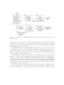
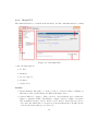
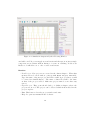
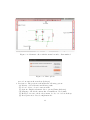
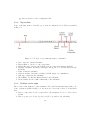
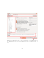
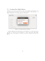
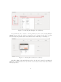
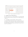
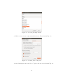
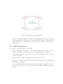
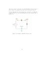
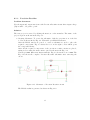
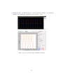
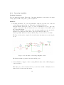
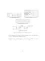
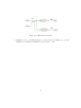
eSim
An open source EDA tool for circuit design,
simulation, analysis and PCB design
eSim User Manual
version 1.0.0
Prepared By:
eSim Team
FOSSEE at IIT,Bombay
Indian Institute of Technology Bombay
\
=
$
BY:
August 2015
Contents
1 Introduction
1
2 Installing eSim
3
3 Architecture of eSim
3.1 Modules used in eSim . . . . . . .
3.1.1 Eeschema . . . . . . . . . .
3.1.2 CvPcb . . . . . . . . . . . .
3.1.3 Pcbnew . . . . . . . . . . .
3.1.4 KiCad to Ngspice converter
3.1.5 Model Builder . . . . . . .
3.1.6 Subcircuit Builder . . . . .
3.1.7 Ngspice . . . . . . . . . . .
3.2 Work flow of eSim . . . . . . . . .
.
.
.
.
.
.
.
.
.
4
4
4
5
5
6
7
7
7
7
4 Getting Started
4.1 eSim Main Window . . . . . . . . . . . . . . . . . . . . . . . . . . . . . .
4.1.1 How to launch eSim in Ubuntu? . . . . . . . . . . . . . . . . . .
4.1.2 Main-GUI . . . . . . . . . . . . . . . . . . . . . . . . . . . . . . .
10
10
10
11
5 Schematic Creation
5.1 Familiarizing the Schematic Editor interface . .
5.1.1 Top menu bar . . . . . . . . . . . . . . .
5.1.2 Top toolbar . . . . . . . . . . . . . . . .
5.1.3 Toolbar on the right . . . . . . . . . . .
5.1.4 Toolbar on the left . . . . . . . . . . . .
5.1.5 Hotkeys . . . . . . . . . . . . . . . . . .
5.2 Schematic creation for simulation . . . . . . . .
5.2.1 Selection and placement of components
5.2.2 Wiring the circuit . . . . . . . . . . . .
5.2.3 Assigning values to components . . . . .
16
16
16
18
18
19
20
20
21
23
23
.
.
.
.
.
.
.
.
.
.
.
.
.
.
.
.
.
.
.
.
.
.
.
.
.
.
.
.
.
.
.
.
.
.
.
.
.
.
.
.
.
.
.
.
.
.
.
.
.
.
.
.
.
.
.
.
.
.
.
.
.
.
.
.
.
.
.
.
.
.
.
.
.
.
.
.
.
.
.
.
.
.
.
.
.
.
.
.
.
.
.
.
.
.
.
.
.
.
.
.
.
.
.
.
.
.
.
.
.
.
.
.
.
.
.
.
.
.
.
.
.
.
.
.
.
.
.
.
.
.
.
.
.
.
.
.
.
.
.
.
.
.
.
.
.
.
.
.
.
.
.
.
.
.
.
.
.
.
.
.
.
.
.
.
.
.
.
.
.
.
.
.
.
.
.
.
.
.
.
.
.
.
.
.
.
.
.
.
.
.
.
.
.
.
.
.
.
.
.
.
.
.
.
.
.
.
.
.
.
.
.
.
.
.
.
.
.
.
.
.
.
.
.
.
.
.
.
.
.
.
.
.
.
.
.
.
.
.
.
.
.
.
.
.
.
.
.
.
.
.
.
.
.
.
.
.
.
.
.
.
.
.
.
.
.
.
.
.
.
.
.
.
.
.
.
.
.
.
.
.
.
.
.
.
.
.
.
.
.
.
.
.
.
.
.
.
.
.
.
.
.
.
.
.
.
.
.
.
.
.
.
.
.
.
.
.
.
.
.
.
5.2.4
5.2.5
Annotation and ERC . . . . . . . . . . . . . . . . . . . . . . . .
Netlist generation . . . . . . . . . . . . . . . . . . . . . . . . . .
6 PCB Design
6.1 Schematic creation for PCB design . . . . . . . . . . .
6.1.1 Netlist generation for PCB . . . . . . . . . . .
6.1.2 Mapping of components using Footprint Editor
6.1.3 Familiarising the Footprint Editor tool . . . . .
6.1.4 Viewing footprints in 2D and 3D . . . . . . . .
6.1.5 Mapping of components in the RC circuit . . .
6.2 Creation of PCB layout . . . . . . . . . . . . . . . . .
6.2.1 Familiarizing the Layout Editor tool . . . . . .
6.2.2 Hotkeys . . . . . . . . . . . . . . . . . . . . . .
6.2.3 PCB design example using RC circuit . . . . .
23
25
.
.
.
.
.
.
.
.
.
.
27
27
27
28
29
30
30
31
32
34
34
7 Model Editor
7.1 Creating New Model Library . . . . . . . . . . . . . . . . . . . . . . . .
7.2 Editing Current Model Library . . . . . . . . . . . . . . . . . . . . . . .
7.3 Uploading external .lib file to eSim repository . . . . . . . . . . . . . . .
43
44
46
46
8 SubCircuit Builder
8.1 Creating a SubCircuit . . . . . . . . . . . . . . . . . . . . . . . . . . . .
8.2 Edit a Subcircuit . . . . . . . . . . . . . . . . . . . . . . . . . . . . . . .
48
49
53
9 Solved Examples
9.1 Solved Examples . . . . . .
9.1.1 Basic RC Circuit . .
9.1.2 Half Wave Rectifier .
9.1.3 Precision Rectifier .
9.1.4 Inverting Amplifier .
9.1.5 Half Adder Example
54
54
54
61
65
69
72
References
.
.
.
.
.
.
.
.
.
.
.
.
.
.
.
.
.
.
.
.
.
.
.
.
.
.
.
.
.
.
.
.
.
.
.
.
.
.
.
.
.
.
.
.
.
.
.
.
.
.
.
.
.
.
.
.
.
.
.
.
.
.
.
.
.
.
.
.
.
.
.
.
.
.
.
.
.
.
.
.
.
.
.
.
.
.
.
.
.
.
.
.
.
.
.
.
.
.
.
.
.
.
.
.
.
.
.
.
.
.
.
.
.
.
.
.
.
.
.
.
.
.
.
.
.
.
.
.
.
.
.
.
.
.
.
.
.
.
.
.
.
.
.
.
.
.
.
.
.
.
.
.
.
.
.
.
.
.
.
.
.
.
.
.
.
.
.
.
.
.
.
.
.
.
.
.
.
.
.
.
.
.
.
.
.
.
.
.
.
.
.
.
.
.
.
.
.
.
.
.
.
.
.
.
.
.
.
.
.
.
.
.
.
.
.
.
.
.
.
.
.
.
.
.
.
.
.
.
.
.
.
.
.
.
.
.
.
.
.
.
77
Chapter 1
Introduction
Electronic systems are an integral part of human life. They have simplified our lives
to a great extent. Starting from small systems made of a few discrete components to
the present day integrated circuits (ICs) with millions of logic gates, electronic systems
have undergone a sea change. As a result, design of electronic systems too have become
extremely difficult and time consuming. Thanks to a host of computer aided design
tools, we have been able to come up with quick and efficient designs. These are called
Electronic Design Automation or EDA tools.
Let us see the steps involved in EDA. In the first stage, the specifications of the
system are laid out. These specifications are then converted to a design. The design
could be in the form of a circuit schematic, logical description using an HDL language,
etc. The design is then simulated and re-designed, if needed, to achieve the desired
results. Once simulation achieves the specifications, the design is either converted to
a PCB, a chip layout, or ported to an FPGA. The final product is again tested for
specifications. The whole cycle is repeated until desired results are obtained [9].
A person who builds an electronic system has to first design the circuit, produce a
virtual representation of it through a schematic for easy comprehension, simulate it and
finally convert it into a Printed Circuit Board (PCB). There are various tools available
that will help us do this. Some of the popular EDA tools are those of Cadence, Synopys,
Mentor Graphics and Xilinx. Although these are fairly comprehensive and high end,
their licenses are expensive, being proprietary.
There are some free and open source EDA tools like gEDA, KiCad and Ngspice. The
main drawback of these open source tools is that they are not comprehensive. Some
of them are capable of PCB design (e.g. KiCad) while some of them are capable of
performing simulations (e.g. gEDA). To the best of our knowledge, there is no open
source software that can perform circuit design, simulation and layout design together.
eSim is capable of doing all of the above.
eSim is a free and open source EDA tool. It is an acronym for Electronics Simulation.
eSim is created using open source software packages, such as KiCad, Ngspice and
Python. Using eSim, one can create circuit schematics, perform simulations and design
PCB layouts. It can create or edit new device models, and create or edit subcircuits for
simulation.
Because of these reasons, eSim is expected to be useful for students, teachers and
other professionals who would want to study and/or design electronic systems. eSim is
also useful for entrepreneurs and small scale enterprises who do not have the capability
to invest in heavily priced proprietary tools.
This book introduces eSim to the reader and illustrates all the features of eSim with
examples. Chapter 2 gives step by step instructions to install eSim on a typical computer
system and to validate the installation. The software architecture of eSim is presented
in Chapter 3. Chapter 4 gets the user started with eSim. It takes them through a tour of
eSim with the help of a simple RC circuit example. Chapter 5 illustrates how to simulate
circuits. Chapter 6 explains PCB design using eSim, in detail. The advanced features
of eSim such as Model Builder covered in Chapter 7 and Sub circuiting is covered in
Chapter 8. Chapter 9 illustrates how to use eSim for solving problems.
The following convention has been adopted throughout this manual.All the menu
names, options under each menu item, tool names, certain points to be noted, etc.,
are given in italics. Some keywords, names of certain windows/dialog boxes, names of
some files/projects/folders, messages displayed during an activity, names of websites,
component references, etc., are given in typewriter font. Some key presses, e.g. Enter
key, F1 key, y for yes, etc., are also mentioned in typewriter font.
2
Chapter 2
Installing eSim
1. eSim installation in Ubuntu:
After downloading the zip file from https://github.com/FOSSEE/eSim to a local
directory unpack it using:
$ unzip eSim.zip
Now change directories in to the top-level source directory (where this INSTALL
file can be found).
To install eSim and other dependecies run the following command.
$ ../install-linux.sh –install
Above script will install eSim along with dependencies.
eSim will be installed to /opt/eSim
To run eSim you can directly run it from terminal as
$ esim
or you can double click on eSim icon created on desktop after installation.
Chapter 3
Architecture of eSim
eSim is a CAD tool that helps electronic system designers to design, test and analyse
their circuits. But the important feature of this tool is that it is open source and hence
the user can modify the source as per his/her need. The software provides a generic,
modular and extensible platform for experiment with electronic circuits. This software
runs on all Ubuntu Linux distributions and some flavours of Windows. It uses Python,
KiCad and Ngspice.
The objective behind the development of eSim is to provide an open source EDA
solution for electronics and electrical engineers. The software should be capable of
performing schematic creation, PCB design and circuit simulation (analog, digital and
mixed signal). It should provide facilities to create new models and components. The
architecture of eSim has been designed by keeping these objectives in mind.
3.1
Modules used in eSim
Various open-source tools have been used for the underlying build-up of eSim. In this
section we will give a brief idea about all the modules used in eSim.
3.1.1
Eeschema
Eeschema is an integrated software where all functions of circuit drawing, control, layout,
library management and access to the PCB design software are carried out. It is the
schematic editor tool used in KiCad [11]. Eeschema is intended to work with PCB layout
software such as Pcbnew. It provides netlist that describes the electrical connections of
the PCB. Eeschema also integrates a component editor which allows the creation, editing
and visualization of components. It also allows the user to effectively handle the symbol
libraries i.e; import, export, addition and deletion of library components. Eeschema
also integrates the following additional but essential functions needed for a modern
schematic capture software: 1. Design rules check (DRC) for the automatic control of
incorrect connections and inputs of components left unconnected. 2. Generation of
layout files in POSTSCRIPT or HPGL format. 3. Generation of layout files printable via
printer. 4. Bill of material generation. 5. Netlist generation for PCB layout or for
simulation. This module is indicated by the label 1 in Fig. 3.1.
As Eeschema is originally intended for PCB Design, there are no fictitious components1 such as voltage or current sources. Thus, we have added a new library for
different types of voltage and current sources such as sine, pulse and square wave. We
have also built a library which gives printing and plotting solutions. This extension,
developed by us for eSim, is indicated by the label 2 in Fig. 3.1.
3.1.2
CvPcb
CvPcb is a tool that allows the user to associate components in the schematic to component footprints when designing the printed circuit board. CvPcb is the footprint
editor tool in KiCad [11]. Typically the netlist file generated by Eeschema does not
specify which printed circuit board footprint is associated with each component in the
schematic. However, this is not always the case as component footprints can be associated during schematic capture by setting the component’s footprint field. CvPcb provides a convenient method of associating footprints to components. It provides footprint
list filtering, footprint viewing, and 3D component model viewing to help ensure that
the correct footprint is associated with each component. Components can be assigned to
their corresponding footprints manually or automatically by creating equivalence files.
Equivalence files are look up tables associating each component with its footprint. This
interactive approach is simpler and less error prone than directly associating footprints
in the schematic editor. This is because CvPcb not only allows automatic association,
but also allows to see the list of available footprints and displays them on the screen to
ensure the correct footprint is being associated. This module is indicated by the label
3 in Fig. 3.1.
3.1.3
Pcbnew
Pcbnew is a powerful printed circuit board software tool. It is the layout editor tool used
in KiCad [11]. It is used in association with the schematic capture software Eeschema,
which provides the netlist. Netlist describes the electrical connections of the circuit.
CvPcb is used to assign each component, in the netlist produced by Eeschema, to a
module that is used by Pcbnew. The features of Pcbnew are given below:
• It manages libraries of modules. Each module is a drawing of the physical component including its footprint - the layout of pads providing connections to the
1
Signal generator or power supply is not a single component but in circuit simulation, we consider
them as a component. While working with actual circuit, signal generator or power supply gives input
to the circuit externally thus, doesn’t require for PCB design.
5
component. The required modules are automatically loaded during the reading of
the netlist produced by CvPcb.
• Pcbnew integrates automatically and immediately any circuit modification by removal of any erroneous tracks, addition of new components, or by modifying any
value (and under certain conditions any reference) of old or new modules, according to the electrical connections appearing in the schematic.
• This tool provides a rats nest display, a hairline connecting the pads of modules
connected on the schematic. These connections move dynamically as track and
module movements are made.
• It has an active Design Rules Check (DRC) which automatically indicates any error
of track layout in real time.
• It automatically generates a copper plane, with or without thermal breaks on the
pads.
• It has a simple but effective auto router to assist in the production of the circuit.
An export/import in SPECCTRA dsn format allows to use more advanced autorouters.
• It provides options specifically for the production of ultra high frequency circuits
(such as pads of trapezoidal and complex form, automatic layout of coils on the
printed circuit).
• Pcbnew displays the elements (tracks, pads, texts, drawings and more) as actual
size and according to personal preferences such as:
– display in full or outline.
– display the track/pad clearance.
This module is indicated by the label 4 in Fig. 3.1.
3.1.4
KiCad to Ngspice converter
We can provide analysis parameters, and the source details through this module. It
also allows us to add and edit the device models and subcircuits, included in the circuit
schematic. Finally, this module facilitates the conversion of KiCad netlist to Ngspice
compatible ones. It is developed by us for eSim and it is indicated by the label 7 in
Fig. 3.1.
6
3.1.5
Model Builder
This tool provides the facility to define a new model for devices such as, 1. Diode
2. Bipolar Junction Transistor (BJT) 3. Metal Oxide Semiconductor Field Effect Transistor (MOSFET) 4. Junction Field Effect Transistor (JFET) 5. IGBT and 6. Magnetic
core. This module also helps edit existing models. It is developed by us for eSim and it
is indicated by the label 5 in Fig. 3.1.
3.1.6
Subcircuit Builder
This module allows the user to create a subcircuit for a component. Once the subcircuit
for a component is created, the user can use it in other circuits. It has the facility to
define new components such as, Op-amps and IC-555. This component also helps edit
existing subcircuits. This module is developed by us for eSim and it is indicated by the
label 6 in Fig. 3.1.
3.1.7
Ngspice
Ngspice is a general purpose circuit simulation program for nonlinear dc, nonlinear transient, and linear ac analysis [12]. Circuits may contain resistors, capacitors, inductors,
mutual inductors, independent voltage and current sources, four types of dependent
sources, lossless and lossy transmission lines (two separate implementations), switches,
uniform distributed RC lines, and the five most common semiconductor devices: diodes,
BJTs, JFETs, MESFETs, and MOSFET. This module is indicated by the label 9 in
Fig. 3.1.
3.2
Work flow of eSim
Fig. 3.1 shows the work flow in eSim. The block diagram consists of mainly three parts:
• Schematic Editor
• PCB Layout Editor
• Circuit Simulators
Here we explain the role of each block in designing electronic systems. Circuit design
is the first step in the design of an electronic circuit. Generally a circuit diagram is drawn
on a paper, and then entered into a computer using a schematic editor. Eeschema is
the schematic editor for eSim. Thus all the functionalities of Eeschema are naturally
available in eSim.
Libraries for components, explicitly or implicitly supported by Ngspice, have been
created using the features of Eeschema. As Eeschema is originally intended for PCB
7
Figure 3.1: Work flow in eSim. (Boxes with dotted lines denote the modules developed
in this work).
design, there are no fictitious components such as voltage or current sources. Thus, a
new library for different types of voltage and current sources such as sine, pulse and
square wave, has been added in eSim. A library which gives the functionality of printing
and plotting has also been created.
The schematic editor provides a netlist file, which describes the electrical connections
of the design. In order to create a PCB layout, physical components are required to be
mapped into their footprints. To perform component to footprint mapping, CvPcb is
used. Footprints have been created for the components in the newly created libraries.
Pcbnew is used to draw a PCB layout.
After designing a circuit, it is essential to check the integrity of the circuit design.
In the case of large electronic circuits, breadboard testing is impractical. In such cases,
electronic system designers rely heavily on simulation. The accuracy of the simulation
results can be increased by accurate modeling of the circuit elements. Model Builder
provides the facility to define a new model for devices and edit existing models. Complex
circuit elements can be created by hierarchical modeling. Subcircuit Builder provides
an easy way to create a subcircuit.
The netlist generated by Schematic Editor cannot be directly used for simulation due
to compatibility issues. Netlist Converter converts it into Ngspice compatible format.
The type of simulation to be performed and the corresponding options are provided
8
through a graphical user interface (GUI). This is called KiCad to Ngspice Converter in
eSim.
eSim uses Ngspice for analog, digital, mixed-level/mixed-signal circuit simulation.
Ngspice is based on three open source software packages [14]:
• Spice3f5 (analog circuit simulator)
• Cider1b1 (couples Spice3f5 circuit simulator to DSIM device simulator)
• Xspice (code modeling support and simulation of digital components through an
event driven algorithm)
It is a part of gEDA project. Ngspice is capable of simulating devices with BSIM, EKV,
HICUM, HiSim, PSP, and PTM models. It is widely used due to its accuracy even for
the latest technology devices.
9
Chapter 4
Getting Started
In this chapter we will get started with eSim. We will run through the various options
available with an example circuit. Referring to this chapter will make one familiar with
eSim and will help plan the project before actually designing a circuit. Lets get started.
4.1
4.1.1
eSim Main Window
How to launch eSim in Ubuntu?
After installation is completed, to launch eSim 1. Go to terminal.
2. Type esim and hit enter.
The first window that appears is workspace dialog as shown in Fig. 4.1.
Figure 4.1: eSim-Workspace
The default workspace is eSim-Workspace under home directory. To create new
workspace use browse option.
4.1.2
Main-GUI
The main GUI window of eSim is as shown in Fig. 4.2 The eSim main window consists
Figure 4.2: eSim Main GUI
of the following symbols.
1. Toolbar
2. Menubar
3. Project explorer
4. Dockarea
5. Console area
Toolbar
• Open Schematic: The first tool on the toolbar i.e. Schematic Editor . Clicking on
this button will open Eeschema, the KiCad schematic editor.
• Convert KiCad to Ngspice: This converter converts KiCad spice netlist into
Ngspice compatible netlist. The KiCad to Ngspice window consists of total five
tabs as namely Analysis, Device Model, Source Details, Model Library, Subcircuits. Once the values have been entered, press the Convert key. It will generate
.cir.out file in the same project directory.
11
Figure 4.3: Toolbar
Note that KiCad to Ngspice Converter can only be used if current project has
created the KiCad spice netlist file .cir.
The details of tabs under KiCad to Ngspice converter are as follows:
Analysis
This feature helps the user to perform different types of analysis such as Operating
point analysis, DC analysis, AC analysis, transient analysis. It has the facility to
– Insert type of analysis such as AC or DC or Transient
– Insert values for analysis
Source Details
eSim sources are added from eSim Sources library. Source such as SINE, AC,
DC, PULSE are in this library. The parameter values to all the sources added in
the shcematic can be given through ’Source Details’.
12
Ngspice Model
Ngspice has in built model such as flipflop(D,SR,JK,T),gain,summer etc. which
can be utilised while building a circuit. eSim allows to add and modify Ngspice
model parameter through Ngspice Model tab.
Device Modeling
Devices like Diode, JFET, MOSFET, IGBT, MOS etc used in the circuit can be
modeled using device model libraries. eSim also provides editing and adding new
model libraries. While converting KiCad to Ngspice, these library files are added
to the corresponding devices used in the circuit.
Subcircuits
Subcircuits are circuits within circuit. Subcircuiting helps to reuse the parts of
the circuits. The subcircuits in the main circuits are added using this facility.
Also, eSim provides us with the facility to edit already existing subcircuits.
• Simulation: The netlist generated using the KiCad to Ngspice converter is simulated using simulation button. Clicking on the Simulation button will run the
Ngspice simulation for current project. Python plotting window will open, as
shown in Fig. 4.4. It shows the output waveform of current project. In the
Ngspice tab we can view the output plotted by Ngspice.
• Foot Print Editor: Clicking on the Footprint Editor tool will open the CvPcb
window. This window will ideally open the .net file for the current project. So,
before using this tool, one should have the netlist for PCB design (a .net file).
• PCB Layout: Clicking on the Layout Editor tool will open Pcbnew, the layout
editor used in eSim. In this window, one will create the PCB. It involves laying tracks and vias, performing optimum routing of tracks, creating one or more
copper layers for PCB, etc. It will be saved as a .brd file in the current project
directory.
• Model Editor: eSim also gives an option to re-configure the model library of a
device. It facilitates the user to change model library of devices such as diode,
transistor, MOSFET, etc.
• Subcircuit: eSim has an option to build subcircuits. The subcircuits can again
have components having subcircuits and so on. This enables users to build commonly used circuits as subcircuits and then use it across circuits. For example, one
13
Figure 4.4: Simulation Output in Python Plotting Window
can build a 12 Volt power supply as a subcircuit and then use it as just a single
component across circuits without having to recreate it. Clicking on Subcircuit
Builder tool will allow one to edit or create a subcircuit.
Menubar
– New Project: New projects are created in the eSim-workspace. When this
menu is selected, a new window opens up with Enter Project name field.
Type the name of the new project and click on OK. A project directory will
be created in eSim-Workspace. The name of this folder will be the same
as that of the project created. Make sure project name does not have any
spaces.
– Open Project: This opens the file dialog of defalut workspace where the
projects are stored. The project can be selected which is then added in the
project explorer.
– Exit: This button closes the project window and exits.
– Help: It opens user manual in the dockarea.
14
Project Explorer
Project explorer has tree of all the project previously added in it. On right clicking
the project we can simply remove or refresh the project in the explorer. Also on
double/right clicking, the project file can be opened in the text editor which can
then be edited.
Dockarea
This area is used to open the following windows.
1. KiCad to Ngspice converter
2. Ngspice plotting
3. Python plotting
4. Model builder
5. Subcircuit builder
Console Area
Console area provides information about the activity done in current project.
15
Chapter 5
Schematic Creation
The first step in the design of an electronic system is the design of its circuit. This
circuit is usually created using a Schematic Editor and is called a Schematic. eSim
uses Eeschema as its schematic editor. Eeschema is the schematic editor of KiCad.
It is a powerful schematic editor software. It allows the creation and modification of
components and symbol libraries and supports multiple hierarchical layers of printed
circuit design.
5.1
Familiarizing the Schematic Editor interface
Fig. 5.1 shows the schematic editor and the various menu and toolbars. We will explain
them briefly in this section.
5.1.1
Top menu bar
The top menu bar will be available at the top left corner. Some of the important menu
options in the top menu bar are:
1. File - The file menu items are given below:
(a) New - Clear current schematic and start a new one
(b) Open - Open a schematic
(c) Open Recent - A list of recently opened files for loading
(d) Save Whole Schematic project - Save current sheet and all its hierarchy.
(e) Save Current Sheet Only - Save current sheet, but not others in a hierarchy.
(f) Save Current sheet as - Save current sheet with a new name.
(g) Print - Access to print menu (See Fig. 5.2).
(h) Plot - Plot the schematic in Postscript, HPGL, SVF or DXF format
(i) Quit - Quit the schematic editor.
2. Place - The place menu has shortcuts for placing various items like components,
wire and junction, on to the schematic editor window. See Sec. 5.1.5 to know
Figure 5.1: Schematic editor with the menu bar and toolbars marked
Figure 5.2: Print options
more about various shortcut keys (hotkeys).
3. Preferences - The preferences menu has the following options:
(a) Library - Select libraries and library paths
(b) Colors - Select colors for various items.
(c) Options - Display schematic editor options (Units, Grid size).
(d) Language - Shows the current list of translations. Use default.
(e) Hotkeys - Access to the hot keys menu. See Sec. 5.1.5 about hotkeys.
(f) Read preferences - Read configuration file.
17
(g) Save preferences - Save configuration file.
5.1.2
Top toolbar
Some of the important tools in the top toolbar are discussed below. They are marked
in Fig. 5.3.
Figure 5.3: Toolbar on top with important tools marked
1.
2.
3.
4.
5.
6.
7.
8.
9.
Save - Save the current schematic
Library Editor - Create or edit components.
Library Browser - Browse through the various component libraries available
Navigate schematic hierarchy - Navigate among the root and sub-sheets in the
hierarchy
Print - Print the schematic
Generate netlist - Generate a netlist for PCB design or for simulation.
Annotate - Annotate the schematic
Check ERC - Do Electric Rules Check for the schematic
Create BOM - Create a Bill of Materials of the schematic
5.1.3
Toolbar on the right
The toolbar on the right side of the schematic editor window has many important tools.
Some of them are marked in Fig. 5.4. Let us now look at each of these tools and their
uses.
1. Place a component - Load a component to the schematic. See Sec. 5.2.1 for more
details.
2. Place a power port - Load a power port (Vcc, ground) to the schematic
18
Figure 5.4: Toolbar on right with important tools marked
3.
4.
5.
6.
7.
Place wire - Draw wires to connect components in schematic
Place bus - Place a bus on the schematic
Place a no connect - Place a no connect flag, particularly useful in ICs
Place a local label - Place a label or node name which is local to the schematic
Place a global label - Place a global label (these are connected across all schematic
diagrams in the hierarchy)
8. Place a text or comment - Place a text or comment in the schematic
5.1.4
Toolbar on the left
Some of the important tools in the toolbar on the left are discussed below. They are
marked in Fig. 5.5.
1. Show/Hide grid - Show or Hide the grid in the schematic editor. Pressing the tool
again hides (shows) the grid if it was shown (hidden) earlier.
2. Show hidden pins - Show hidden pins of certain components, for example, power
pins of certain ICs.
19
Figure 5.5: Toolbar on left with important tools marked
5.1.5
Hotkeys
A set of keyboard keys are associated with various operations in the schematic editor.
These keys save time and make it easy to switch from one operation to another. The list
of hotkeys can be viewed by going to Preferences in the top menu bar. Choose Hotkeys
and select List current keys. The hotkeys can also be edited by selecting the option Edit
Hotkeys. Some frequently used hotkeys, along with their functions, are given below:
• F1 - Zoom in
• F2 - Zoom out
• Ctrl + Z - Undo
• Delete - Delete item
• M - Move item
• C - Copy item
• A - Add/place component
• P - Place power component
• R - Rotate item
• X - Mirror component about X axis
• Y - Mirror component about Y axis
• E - Edit schematic component
• W - Place wire
• T - Add text
• S - Add sheet
Note: Both lower and upper-case keys will work as hotkeys.
5.2
Schematic creation for simulation
There are certain differences between the schematic created for simulation and that
created for PCB design. We need certain components like plots and current sources.
For simulation whereas these are not needed for PCB design. For PCB design, we
20
would require connectors (e.g. DB15 and 2 pin connector) for taking signals in and out
of the PCB whereas these have no meaning in simulation. This section covers schematic
creation for simulation.
The first step in the creation of circuit schematic is the selection and placement of
required components. The components are grouped under eSim-libraries as shown in
Fig. 5.6.
Figure 5.6: eSim-Components Libraries
5.2.1
Selection and placement of components
We would need a resistor, a capacitor, a voltage source, ground terminal. To place a
resistor on the schematic editor window, select the Place a component tool from the
toolbar on the right side and click anywhere on the schematic editor. This opens up
the component selection window. Resistor component can be found under eSim Devices
library. Fig. 5.7 shows the selection of resistor component. Click on OK. A resistor will
be tied to the cursor. Place the resistor on the schematic editor by a single click.
To place the next component, i.e., capacitor, click again on the schematic editor.Similarly, Capacitor component is found under eSim Devices library. Click on OK.
Place the capacitor on the schematic editor by a single click. Let us now place a sinusoidal voltage source. This is required for performing transient analysis. To place it,
click again on the schematic editor. On the component selection window, choose the
library eSim source by double clicking on it. Select the component SINE and click on
OK. Place the sine source on the schematic editor by a single click.
Place the component by clicking on the schematic editor. Similarly place gnd, a
21
Figure 5.7: Placing a resistor using the Place a Component tool
ground terminal and power flag under power library. Once all the components are
placed, the schematic editor would look like the Fig. 5.8. Let us rotate the resistor to
Figure 5.8: All RC circuit components placed
complete the circuit. To rotate the resistor, place the cursor on the resistor and press
the key R. Note that if the cursor is placed above the letter R (not R?) on the resistor,
it asks to clarify selection. Choose the option Component R. This can be avoided by
placing the cursor slightly away from the letter R as shown in Fig. 5.9. This applies
to all components. If one wants to move a component, place the cursor on top of the
22
Figure 5.9: Placing the cursor (cross mark) slightly away from the letter R
component and press the key M. The component will be tied to the cursor and can be
moved in any direction.
5.2.2
Wiring the circuit
The next step is to wire the connections. Let us connect the resistor to the capacitor.
To do so, point the cursor to the terminal of resistor to be connected and press the key
W. It has now changed to the wiring mode. Move the cursor towards the terminal of the
capacitor and click on it. A wire is formed as shown in Fig. 5.10a. Similarly connect
(a) Initial stages
(b) Wiring done
(c)
Final
schematic
PWR FLAG
with
Figure 5.10: Various stages of wiring
the wires between all terminals and the final schematic would look like Fig. 5.10b.
5.2.3
Assigning values to components
We need to assign values to the components in our circuit i.e., resistor and capacitor.
Note that the sine voltage source has been placed for simulation. The specifications of
sine source will be given during simulation. To assign value to the resistor, place the
cursor above the letter R (not R?) and press the key E. Choose Field value. Type 1k in
the Edit value field box as shown in Fig. 5.11. 1k means 1kΩ. Similarly give the value
1u for the capacitor. 1u means 1µF .
5.2.4
Annotation and ERC
The next step is to annotate the schematic. Annotation gives unique references to the
components. To annotate the schematic, click on Annotate schematic tool from the top
23
Figure 5.11: Editing value of resistor
toolbar. Click on annotation, then click on OK and finally click on close as shown in
Fig. 5.13. The schematic is now annotated. The question marks next to component
references have been replaced by unique numbers. If there are more than one instance
of a component (say resistor), the annotation will be done as R1, R2, etc.
Let us now do ERC or Electric Rules Check. To do so, click on Perform electric
rules check tool from the top toolbar. Click on Test Erc button. The error as shown
in Fig. 5.12 may be displayed. Click on close in the test erc window. There will be
Figure 5.12: ERC error
a green arrow pointing to the source of error in the schematic. Here it points to the
ground terminal. This is shown in Fig. 5.14. To correct this error, place a PWR FLAG
from the Eeschema library power. Connect the power flag to the ground terminal as
shown in Fig. 5.10c. One needs to place PWR FLAG wherever the error shown in Fig. 5.12
24
Figure 5.13: Steps in annotating a schematic: 1. First click on Annotation then 2. Click
on Ok then 3. Click on close
Figure 5.14: Green arrow pointing to Ground terminal indicating an ERC error
is obtained. Repeat the ERC. Now there are no errors. With this we have created the
schematic for simulation.
5.2.5
Netlist generation
To simulate the circuit that has been created in the previous section, we need to generate
its netlist. Netlist is a list of components in the schematic along with their connection
information. To do so, click on the Generate netlist tool from the top toolbar. Click on
spice from the window that opens up. Check the option Default Format. Then click
on Generate. This is shown in Fig. 5.15. Save the netlist. This will be a .cir file. Do
not change the directory while saving. Now the netlist is ready to be simulated. Refer
to [15] or [16] to know more about Eeschema.
25
Figure 5.15: Steps in generating a Netlist for simulation: 1. Click on Spice then 2.
Check the option Default Format then 3. Click on Generate
26
Chapter 6
PCB Design
Printed Circuit Board (PCB) design is an important step in electronic system design.
Every component of the circuit needs to be placed and connections routed to minimise
delay and area. Each component has an associated footprint. Footprint refers to the
physical layout of a component that is required to mount it on the PCB. PCB design involves associating footprints to all components, placing them appropriately to minimise
wire length and area, connecting the footprints using tracks/vias and finally extracting
the required files needed for printing the PCB. Let us see the steps to design PCB using
eSim.
6.1
Schematic creation for PCB design
In Chapter 9, we will see the differences between schematic for simulation and schematic
for PCB design. Let us design the PCB for a RC circuit. A resistor, capacitor, ground,
power flag and a connector are required. Connectors are used to take signals in and out
of the PCB.
Create the circuit schematic as shown in Fig. 6.1. The two pin connector (CONN 2 )
can be placed from the Eeschema library conn. Do the annotation and test for ERC.
Refer to Chapter 9 to know more about basic steps in schematic creation.
6.1.1
Netlist generation for PCB
The netlist for PCB is different from that for simulation. To generate netlist for PCB,
click on the Generate netlist tool from the top toolbar in Schematic editor. In the
Netlist window, under the tab Pcbnew, click on the button Netlist. This is shown in
Fig. 6.2. Click on Save in the Save netlist file dialog box that opens up. Do not change
the directory or the name of the netlist file. Save the schematic and close the schematic
editor. Note that the netlist for PCB has an extension .net. The netlist created for
simulation has an extension .cir.
Figure 6.1: Final circuit schematic for RC low pass circuit
Figure 6.2: Netlist generation for PCB
6.1.2
Mapping of components using Footprint Editor
Once the netlist for PCB is created, one needs to map each component in the netlist to
a footprint. The tool Footprint Editor is used for this. eSim uses CvPcb as its footprint
editor. CvPcb is the footprint editor tool in KiCad.
28
Figure 6.3: Footprint editor with the menu bar, toolbar, left pane and right pane marked
6.1.3
Familiarising the Footprint Editor tool
If one opens the Footprint Editor after creating the .net netlist file, the Footprint
editor as shown in Fig. 6.3 will be obtained. The menu bar and toolbars and the panes
are marked in this figure. The menu bar will be available in the top left corner. The
left pane has a list of components in the netlist file and the right pane has a list of
available footprints for each component. Note that if the Footprint Editor is opened
before creating a ‘.net’ file, then the left and right panes will be empty.
Toolbar
Some of the important tools in the toolbar are shown in Fig. 6.4. They are explained
below:
1. Save netlist and footprint files - Save the netlist and the footprints that are associated with it.
2. View selected footprint - View the selected footprint in 2D. See Sec. 6.1.4 for more
details.
3. Automatic footprint association - Perform footprint association for each component automatically. Footprints will be selected from the list of footprints available.
4. Delete all associations - Delete all the footprint associations made
5. Display filtered footprint list - Display a filtered list of footprints suitable to the
29
Figure 6.4: Some important tools in the toolbar
selected component
6. Display full footprint list - Display the list of all footprints available (without
filtering)
6.1.4
Viewing footprints in 2D and 3D
To view a footprint in 2D, select it from the right pane and click on View selected
footprint from the menu bar. Let us view the footprint for SM1210. Choose SM1210
from the right pane as shown in Fig. 6.5. On clicking the View selected footprint tool,
the Footprint window with the view in 2D will be displayed. Click on the 3D tool in
the Footprint window, as shown in Fig. 6.6. A top view of the selected footprint in
3D is obtained. Click on the footprint and rotate it using mouse to get 3D views from
various angles. One such side view of the footprint in 3D is shown in Fig. 6.7.
6.1.5
Mapping of components in the RC circuit
Click on C1 from the left pane. Choose the footprint C1 from the right pane by double
clicking on it. Click on connector P1 from the left pane. Choose the footprint SIL-2
from the right pane by double clicking on it. Similarly choose the footprint R3 for the
resistor R1. The footprint mapping is shown in Fig. 6.8. Save the footprint association
by clicking on the Save netlist and footprint files tool from the CvPcb toolbar. The
Save Net and component List window appears. Browse to the directory where the
schematic file for this project is saved and click on Save. The netlist gets saved and
the Footprint Editor window closes automatically. Note that one needs to browse to the
directory where the schematic file is saved and save the ‘.net’ file in the same directory.
30
Figure 6.5: Viewing footprint for SM1210: 1. Choose the footprint SM1210 from the
right pane, 2. Click on View selected footprint
Figure 6.6: Footprint view in 2D. Click on 3D to get 3D view
6.2
Creation of PCB layout
The next step is to place the footprints and lay tracks between them to get the layout.
This is done using the Layout Editor tool. eSim uses Pcbnew, the layout creation tool
in KiCad, as its layout editor.
31
Figure 6.7: Side view of the footprint in 3D
Figure 6.8: Footprint mapping done
6.2.1
Familiarizing the Layout Editor tool
The layout editor with the various menu bar and toolbars is shown in Fig. 6.9.
32
Figure 6.9: Layout editor with menu bar, toolbars and layer options marked
Figure 6.10: Top toolbar with important tools marked
Top toolbar
Some of the important menu options in the top menu bar are shown in Fig. 6.10. They
are explained below:
1. Save board - Save the printed circuit board
2. Module editor - Open module editor to edit footprint modules or libraries
3. Read netlist - Import the netlist whose layout needs to be created.
33
4. Perform design rules check - Check for design rules, unconnected nets, etc., in the
layout.
5. Select working layer - Selection of working layer
6. Show active layer selections and select layer pair for route and place - Select layer
in top and bottom layers. It also shows the currently active layer selections.
7. Mode footprint: Manual/automatic move and place - Move and place modules
6.2.2
Hotkeys
A list of hotkeys are given below:
1. F1 - Zoom in
2. F2 - Zoom out
3. Delete - Delete Track or Footprint
4. X - Add new track
5. V - Add Via
6. M - Move Item
7. F - Flip Footprint
8. R - Rotate Item
9. G - Drag Footprint
10. Ctrl+Z - Undo
11. E - Edit Item
The list can be viewed by selecting Preferences from the top menu bar and choosing
List Current Keys from the option Hotkeys.
6.2.3
PCB design example using RC circuit
Click on Layout Editor from the eSim toolbar. Click on Read Netlist tool from the top
toolbar. Click on Browse Netlist files on the Netlist window that opens up. Select the
.net file that was modified after assigning footprints. Click on Open. Now Click on Read
Current Netlist on the Netlist window. The message area in the Netlist window says
that the RC pcb.net has been read. The sequence of operations is shown in Fig. 6.11.
The footprint modules will now be imported to the top left hand corner of the layout
editor window. This is shown in Fig. 6.12. Zoom in to the top left corner by pressing the
key F1 or using the scroll button of the mouse. The zoomed in version of the imported
netlist is shown in Fig. 6.13.
Let us now place this in the center of the layout editor window. Click on Mode
footprint: Manual/automatic move and place tool from the top toolbar. Place the
cursor near the center of the layout editor window. Right click and choose Glob move
and place. Choose move all modules. The sequence of operations is shown in Fig. 6.14.
Click on Yes on the confirmation window to move the modules. Zoom in using the F1
key. The current placement of components after zooming in is shown in Fig. 6.15a. We
need to arrange the modules properly to lay tracks. Rotate the connector P1 by placing
34
Figure 6.11: Importing netlist file to layout editor: 1. Browse netlist Files, 2. Choose
the RC pcb.net file, 3. Read Netlist file, 4. Close
Figure 6.12: Footprint modules imported to top left corner of layout editor window
the cursor on top of P1 and pressing R. Move it by placing the cursor on top of it and
pressing M. The final placement is shown in Fig. 6.15b.
Let us now lay the tracks. Let us first change the track width. Click on Design rules
from the top menu bar. Click on Design rules. This is shown in Fig. 6.16. The Design
Rules Editor window opens up. Here one can edit the various design rules. Double click
on the track width field to edit it. Type 0.8 and press Enter. Click on OK. Fig. 6.17
35
Figure 6.13: Zoomed in version of the imported netlist
Figure 6.14: Moving and placing modules to the center of layout editor. 1. Click on
Mode footprint: Manual/automatic move and place, 2. Place cursor at center of layout
editor and right click on it 3. Choose Glob Move and Place and then choose Move All
Modules.
shows the sequence of operations.
Click on Back from the Layer options as shown in Fig. 6.18. Let us now start
laying the tracks. Place the cursor above the left terminal of R1 in the layout editor
window. Press the key x. Move the cursor down and double click on the left terminal
of C1. A track is formed. This is shown in Fig. 6.19a. Similarly lay the track between
36
(a) Zoomed in version of the current placement after moving modules to the center of
the layout editor
(b) Final placement of footprints after rotating and moving P1
Figure 6.15: Different stages of placement of modules on PCB
Figure 6.16: Choose Design Rules from the top menu bar and Design Rules again
capacitor C1 and connector P1 as shown in Fig. 6.19b. The last track needs to be laid
at an angle. To do so, place the cursor above the second terminal of R1. Press the
key x and move the cursor diagonally down. Double click on the other terminal of the
connector. The track will be laid as shown in Fig. 6.19c. All tracks are now laid. The
next step is to create PCB edges.
Choose PCB edges from the Layer options to add edges. Click on Add graphic line
or polygon from the toolbar on the left. Fig. 6.20 shows the sequence of operations.
37
Figure 6.17: Changing the track width: 1. Double click on Track Width field and type
0.8, 2. Click on OK
Let us now start drawing edges for PCB. Click to the left of the layout. Move cursor
horizontally to the right. Click once to change orientation. Move cursor vertically down.
Draw the edges as shown in Fig. 6.21. Double click to finish drawing the edges.
Click on Perform design rules check from the top toolbar to check for design rules.
The DRC Control window opens up. Click on Start DRC. There are no errors under
the Error messages tab. Click on OK to close DRC control window. Fig. 6.22 shows
the sequence of operations. Click on Save board on the top toolbar.
To generate Gerber files, click on File from the top menu bar. Click on Plot. This is
shown in Fig. 6.23. The plot window opens up. One can choose which layers to plot by
selecting/deselecting them from the Layers pane on the left side. One can also choose
the format used to plot them. Choose Gerber. The output directory of the plots created
can also be chosen. By default, it is the project directory. Some more options can be
chosen in this window. Click on Plot. The message window shows the location in which
the Gerber files are created. Click on Close. This is shown in Fig. 6.24. The PCB
design of RC circuit is now complete. To know more about Pcbnew, refer to [15] or [16].
38
Figure 6.18: Choosing the copper layer Back
(a) A track formed between resistor and capacitor
(b) A track formed between capacitor and connector
(c) A track formed between connector and resistor
Figure 6.19: Different stages of laying tracks during PCB design
39
Figure 6.20: Creating PCB edges: 1. Choose PCB Edges from Layer options 2. Choose
Add graphic line or polygon from left toolbar
Figure 6.21: PCB edges drawn
40
Figure 6.22: Performing design rules check: 1. Click on Start DRC, 2. Click on Ok
Figure 6.23: Choosing Plot from the File menu
41
Figure 6.24: Creating Gerber files: 1. Choose Gerber as the plot format, 2. Click on
Plot. Message window shows location in which Gerber files are created, 3. Click on
Close
42
Chapter 7
Model Editor
Spice based simulators include a feature which allows accurate modeling of semiconductor devices such as diodes, transistors etc. eSim Model Editor provides a facility to
define a new model for devices such as diodes, MOSFET, BJT, JFET, IGBT, Magnetic
core etc. Model Editor in eSim lets the user enter the values of parameters depending on
the type of device for which a model is required. The parameter values can be obtained
from the data-sheet of the device. A newly created model can be exported to the model
library and one can import it for different projects, whenever required. Model Editor
also provides a facility to edit existing models. The GUI of the model editor is as shown
in Fig. 7.1
Figure 7.1: Model Editor
43
7.1
Creating New Model Library
eSim lets us create new model libraries based on the template model libraries. On
selecting New button the window is popped as shown in Fig. 7.2. The name has to be
unique otherwise the error message appears on the window.
Figure 7.2: Creating New Model Library
After the OK button is pressed the type of model library to be created is chosen by
selecting one of the types on the left hand side i.e. Diode, BJT, MOS, JFET, IGBT,
Magnetic Core. The template model library opens up in a tabular form as shown in
Fig. 7.3
44
Figure 7.3: Choosing the Template Model Library
New parameters can be added or current parameters can be removed using ADD and
REMOVE buttons. Also the values of parameters can be changed in the table. Adding
and removing the parameters in library files is shown in the Fig. 7.4 and Fig. 7.5
Figure 7.4: Adding the Parameter in a Library
After the editing of the model library is done, the file can be saved by selecting the
SAVE button. These libraries are saved in the User Libraries folder under deviceModelLibrary repository.
45
Figure 7.5: Removing a Parameter from a Library
7.2
Editing Current Model Library
The existing model library can be modified using EDIT option. On clicking the EDIT
button the file dialog opens where all the library files are saved as shown in Fig. 7.6.
You can select the library you want to edit. Once you are done with the editing, click
on SAVE button.
7.3
Uploading external .lib file to eSim repository
eSim directly cannot use the external .lib file. It has to be uploaded to eSim repository
before using it in a circuit. eSim provides the facility to upload library files. They are
then converted into xml format, which can be easily modified from the eSim interface.
On clicking UPLOAD button the library can be uploaded from any location. The model
library will be saved with the name you have provided, in the User Libraries folder of
repository deviceModelLibrary.
46
Figure 7.6: Editing Existing Model Library
47
Chapter 8
SubCircuit Builder
Subcircuit is a way to implement hierarchical modeling. Once a subcircuit for a component is created, it can be used in other circuits. eSim provides an easy way to create a
subcircuit. The following Fig. 8.1 shows the window that is opened when the SubCircuit
tool is chosen from the toolbar.
Figure 8.1: Subcircuit Window
48
8.1
Creating a SubCircuit
The steps to create subcircuit are as follows.
• After opening the Subcircuit tool, click on New Subcircuit Schematic button.
It will ask the name of the subcircuit. Enter the name of subcircuit (without any
spaces) and click OK as shown in Fig. 8.2.
Figure 8.2: New Sub circuit Window
• After clicking OK button it will open KiCad schematic. Draw your circuit which
will be later used as a subcircuit. e.g the Fig. 8.3 shows the half adder circuit.
49
Figure 8.3: New Sub circuit Window
• Once you complete the circuit, assign port to the node of your circuit which will
be used to connect with the main circuit. The circuit will look like Fig. 8.4 after
adding PORT to it. The PORT symbol can be found in Eeschema as shown in
Fig. 8.5.
Figure 8.4: Half-Adder Subcircuit
50
Figure 8.5: Selection of PORT component
• Next step is to save the schematic and generate KiCad netlist as explained in
Chapter 5.
• To use this as a subcircuit, create a block in KiCad Eeschema by following steps
given below:
1. Go to library browser of Eeschema.
2. Select the working library as eSim Subckt as shown in Fig. 8.6
51
Figure 8.6: Selecting Working Library
3. Click on create a new component with reference X as shown in Fig. 8.7
Figure 8.7: Creating New Component
4. Start drawing the subcircuit block. Update and save it as shown in Fig. 8.8.
52
Figure 8.8: Half-Adder Subcircuit Block
• Close the Eeschema window and click on Convert KiCad to Ngspice button in
subcircuit builder tool. This will convert the KiCad spice netlist to Ngspice netlist.
And it will save your subcircuit into eSim repository, which you can add in your
main circuit.
8.2
Edit a Subcircuit
The steps to edit a subcircuit are as follows.
• After opening the Subcircuit tool, click on Edit Subcircuit Schematic button.
It will open a dialog box where you can select any subcircuit for editing.
• After selecting the subcircuit it will open it in KiCad Eeschema, where you can
edit the subcircuit.
• Next step is to save the schematic and generate KiCad netlist.
• If you have edited the number of ports then you have to change the block in KiCad
Eeschema accordingly.
• Close the Eeschema window and click on Convert KiCad to Ngspice button in
subcircuit builder tool to convert the edited subcircuit KiCad netlist into Ngspice
netlist.
53
Chapter 9
Solved Examples
9.1
Solved Examples
9.1.1
Basic RC Circuit
Problem Statement:
Plot the Input and Output Waveform of an RC circuit whose input voltage (Vs) is
50Hz, 3V peak to peak. The values of Resistor (R) and Capacitor(C) are 1k and 1uf
respectively.
Solution:
• Creating a Project: The new project is created by clicking the New icon on the
menubar. The name of the project is given in the pop up window as shown in
Fig. 9.1.
• Creating the Schematic: To create the schematic, click the very first icon of the
left toolbar as shown in the Fig. 9.2. This will open KiCad Eeschema.
To create a schematic in KiCad, we need to place the required components. Fig. 9.3
shows the icon on the right toolbar which opens the component library.
Figure 9.1: Creating New Project
Figure 9.2: Open Schematic Editor
55
Figure 9.3: Place Component Icon
After all the required components of the simple RC circuit are placed, wiring is
done using the Place Wire option as shown in the Fig. 9.4
Figure 9.4: Place Wire Icon
Next step is ERC (Electric Rules Check). Fig. 9.5 shows the icon for ERC.
56
Figure 9.5: Electric Rules Check Icon
Fig. 9.6 shows the RC circuit after connecting the components by wire.
Figure 9.6: RC circuit
57
After clicking the ERC icon a window opens up. Click the Run button to run rules
check. The errors are listed in as shown in Fig. 9.7a. This error is handled by
adding Power Flag as shown in Fig. 9.7b.
(a) ERC Run
(b) Power Flag
Figure 9.7: ERC check and POWER FLAG
After adding the Power Flag the completed RC circuit is shown in Fig. 9.8a and
the netlist is generated as shown in Fig. 9.8b.
(a) Schematic of RC circuit
(b) Generating KiCad Netlist of RC circuit
Figure 9.8: RC Schematic and Netlist Generation
58
• Convert KiCad to Ngspice: To convert KiCad netlist of RC circuit to NgSpice
compatible netlist click on KiCad to Ngspice icon as shown in Fig. 9.9.
Figure 9.9: Convert KiCad to Ngspice Icon
Now you can enter the type of analysis and source details as shown in Fig. 9.10a
and Fig. 9.10b respectively.
(a) RC Analysis
(b) RC Source Details
Figure 9.10: RC Analysis and Source Detail
The other tab will be empty as RC circuit do not use any Ngspice model, device
library and subcircuit.
After entering the value, press the convert button. It will convert the netlist into
Ngspice compatible netlist.
59
• Simulation: To run Ngspice simulation click the simulation icon in the tool bar as
shown in the Fig. 9.11.
Figure 9.11: Simulation Icon
In eSim, there are two types of plot. First is normal Ngspice plot and second is
interactive python plot as shown in Fig. 9.12a and Fig. 9.12b respectively.
In the interactive python plot you can select any node or branch to plot voltage
or current across it. Also it has the facility to plot basic functions across the node
like addition, substraction, multiplication, division and v/s.
60
(a) Ngspice Plot of RC
(b) Python Plot of RC
Figure 9.12: Ngspice and Interactive Python Plotting
9.1.2
Half Wave Rectifier
Problem Statement:
Plot the Input and Output Waveform of Half Wave Rectifier circuit where the input
voltage (Vs) is 50Hz, 2V peak to peak. The value for Resistor (R) is 1k.
Solution:
The new project is created by clicking the New icon on the menubar. The name of the
project is given in the window shown in Fig. 9.1.
• Creating Schematic: To create the schematic, click the very first icon of the left
toolbar as shown in the Fig. 9.2. This will open KiCad Eeschema.
After the KiCad window is opened, to create a schematic we need to place the
required components. Fig. 9.3 shows the icon on the right toolbar which opens
the component library.
61
After all the required components of the simple Half Wave rectifier circuits are
placed, wiring is done using the Place Wire option as shown in the Fig. 9.4
Next step is ERC (Electric Rules Check). Fig. 9.5 shows the icon for ERC. After
completing all the above steps the final Half Wave Rectifier schematic will look
like Fig. 9.13.
Figure 9.13: Schematic of Half Wave Rectifier circuit
62
KiCad netlist is generated as shown in the Fig. 9.14
Figure 9.14: Half Wave Rectifier circuit Netlist Generation
• Convert KiCad to Ngspice: After creating KiCad netlist, click on the KiCad-Ngspice
converter button. This will open converter window where you can enter details
of Analysis, Source values and Device library.
(a) Half Wave Rectifier Analysis
(b) Half Wave Rectifier Source Details
(c) Half Wave Rectifier Device Modeling
Figure 9.15: Analysis, Source and Device Tab
Under device library you can add the library for diode used in the circuit. If you
do not add any library it will take default Ngspice model.
63
• Simulation: Once the KiCad-Ngspice converter runs successfully, you can run
simulation by clicking the simulation button in the toolbar.
(a) Ngspice Plot of Half Wave Rectifier
(b) Python Plot of Half Wave Rectifier
Figure 9.16: Half Wave Rectifier Simulation Output
64
9.1.3
Precision Rectifier
Problem Statement:
Plot the input and output waveform of the Precision Rectifier circuit where input voltage
(Vs) is 50Hz , 3V peak to peak.
Solution:
The new project is created by clicking the New icon on the menubar. The name of the
project is given as shown in the Fig. 9.1.
• Creating Schematic: To create the schematic, click the very first icon of the left
toolbar as shown in the Fig. 9.2. This will open KiCad Eeschema.
After the KiCad window is opened, to create a schematic we need to place the
required components. Fig. 9.3 shows the icon on the right toolbar which opens
the component library.
After all the required components of the precision rectifier circuit are placed,
wiring is done using the Place Wire option as shown in the Fig. 9.4.
Next step is ERC (Electric Rules Check). Fig. 9.5 shows the icon for ERC. The
Fig. 9.17 shows the complete Precision Rectifier schematic after removing the
errors.
Figure 9.17: Schematic of Precision Rectifier circuit
The KiCad netlist is generated as shown in Fig. 9.18.
65
Figure 9.18: Precision Rectifier circuit Netlist Generation
• Convert KiCad to Ngspice: After creating KiCad netlist, click on KiCad-Ngspice
converter button.
This will open converter window where you can enter details of Analysis, Source
values, Device library and Subcircuit.
(a) Precision Rectifier Analysis
(b) Precision Rectifier Source Details
(c) Precision Rectifier Device Modeling
(d) Precision Rectifier Subcircuit
Figure 9.19: Analysis, Source, Device library and Subcircuit tab
Under device library you can add the library for the diode used in the circuit. If
you do not add any library it will take default Ngspice model for diode.
66
Under subcircuit tab you have to add the subciruit used in your circuit. If you
forget to add subcircuit it will throw an error.
67
• Simulation: Once the KiCad-Ngspice converter runs successfully, you can run the
simulation by clicking the simulation button in the toolbar.
(a) Ngspice Plot of Precision Rectifier
(b) Python Plot of Precision Rectifier
Figure 9.20: Precision Rectifier Simulation Output
68
9.1.4
Inverting Amplifier
Problem Statement:
Plot the Input and Output Waveform of Inverting Amplifier circuit where the input
voltage (Vs) is 50Hz, 2V peak to peak and gain is 2.
Solution:
• Creating Schematic: To create the schematic, click the very first icon of the left
toolbar as shown in the Fig. 9.2. This will open KiCad Eeschema.
After the KiCad window is opened, to create a schematic we need to place the
required components. Fig. 9.3 shows the icon on the right toolbar which opens
the component library.
After all the required components of the inverting amplifier circuit are placed,
wiring is done using the Place Wire option as shown in the Fig. 9.4.
Next step is ERC (Electric Rules Check). Fig. 9.5 shows the icon for ERC.
The Fig. 9.21 shows the complete Precision Rectifier schematic after removing the
errors.
Figure 9.21: Schematic of Inverting Amplifier circuit
The KiCad netlist is generated as shown in Fig. 9.22.
• Convert KiCad to Ngspice: After creating KiCad netlist, click on KiCad-Ngspice
converter button.
This will open converter window where you can enter details of Analysis, Source
values, Device library and Subcircuit.
69
Figure 9.22: Inverting Amplifier circuit Netlist Generation
Subcircuit of Op-Amp is shown in Fig. 9.23d
70
(a) Inverting Amplifier Analysis
(b) Inverting Amplifier Source Details
(c) Inverting Amplifier Subcircuit
(d) Sub-Circuit of Op-Amp
Figure 9.23: Analysis, Source, and Subcircuit tab
Under subcircuit tab you have to add the subciruit used in your circuit. If you
forget to add subcircuit, it will throw an error.
• Simulation: Once the KiCad-Ngspice converter runs successfully, you can run
simulation by clicking the simulation button in the toolbar.
71
(a) Inverting Amplifier Ngspice Plot
(b) Inverting Amplifier Python Plot
Figure 9.24: Inverting Amplifier Simulation Output
9.1.5
Half Adder Example
Problem Statement:
Plot the Input and Output Waveform of Half Adder circuit.
Solution:
• Creating Schematic: To create the schematic, click the very first icon of the left
toolbar as shown in the Fig. 9.2. This will open KiCad Eeschema.
After the KiCad window is opened, to create a schematic we need to place the
required components. Fig. 9.3 shows the icon on the right toolbar which opens
the component library.
After all the required components of the Half Adder circuit are placed, wiring is
72
done using the Place Wire option as shown in the Fig. 9.4.
Next step is ERC (Electric Rules Check). Fig. 9.5 shows the icon for ERC.
The Fig. 9.25 shows the complete Half Adder schematic after removing the errors.
Figure 9.25: Schematic of Half Adder circuit
The KiCad netlist is generated as shown in Fig. 9.26.
Figure 9.26: Half Adder circuit Netlist Generation
73
• Convert KiCad to Ngspice: After creating KiCad netlist click on KiCad-Ngspice
converter button.
This will open converter window where you can enter details of Analysis, Source
values, Ngspice model and Subcircuit.
(a) Half Adder Analysis
(b) Half Adder Source Details
(c) Half Adder Ngspice Model
(d) Half Adder Subcircuit Model
Figure 9.27: Analysis, Source, Ngspice Model and Subcircuit tab
Subcircuit of Half Adder in Fig. 9.28
74
Figure 9.28: Half Adder Subcircuit
• Simulation: Once the KiCad-Ngspice converter runs successfully, you can run
simulation by clicking the simulation button in the toolbar.
75
(a) Half Adder Ngspice Plot
(b) Half Adder Python Plot
Figure 9.29: Half Adder Simulation Output
76
References
[1] A. S. Sedra and K. C. Smith, Microelectronic Circuits - Theory and Applications.
Oxford University Press, 2009.
[2] K. M. Moudgalya, “Spoken Tutorial: A Collaborative and Scalable Education Technology,” CSI Communications, vol. 35, no. 6, pp. 10–12, September 2011, available
at http://spoken-tutorial.org/CSI.pdf.
[3] (2013, May). [Online]. Available: http://www.scilab.org/
[4] (2013, May). [Online]. Available: http://scilab-test.garudaindia.in/scilab in/,http:
//scilab-test.garudaindia.in/cloud
[5] D. B. Phatak. (2013, May) Teach 10,000 teacher programme. [Online]. Available:
http://www.it.iitb.ac.in/nmeict/MegaWorkshop.do
[6] K. Kannan and K. Narayanan, “Ict-enabled scalable workshops for engineering
college teachers in india,” in Post-Secondary Education and Technology: A Global
Perspective on Opportunities and Obstacles to Development (International and Development Education), R. Clohey, S. Austin-Li, and J. C. Weldman, Eds. Palgrave
Macmillan, 2012.
[7] (2013, May) Teach 10,000 teacher programme on analog electronics. [Online].
Available: http://www.nmeict.iitkgp.ernet.in/Analogmain.htm
[8] (2013, May). [Online]. Available: http://www.aakashlabs.org/
[9] (2013, May). [Online]. Available: http://en.wikipedia.org/wiki/Electronic design
automation
[10] (2013, May) Synaptic Package Manager Spoken Tutorial. [Online]. Available: http:
//www.spoken-tutorial.org/list videos?view=1&foss=Linux&language=English
[11] (2013, May). [Online]. Available:
KiCad+EDA+Software+Suite
http://www.kicad-pcb.org/display/KICAD/
77
[12] (2013, May). [Online]. Available: http://ngspice.sourceforge.net/
[13] (2013, May). [Online]. Available: http://scilab.in/
[14] S. M. Sandler and C. Hymowitz, SPICE Circuit Handbook. New York: McGrawHill Professional, 2006.
[15] J.-P. Charras and F. Tappero. (2013, May). [Online]. Available:
//www.kicad-pcb.org/display/KICAD/KiCad+Documentation
http:
[16] D. Jahshan and P. Hutchinson. (2013, May). [Online]. Available: http:
//bazaar.launchpad.net/∼kicad-developers/kicad/doc/files/head:/doc/tutorials/
[17] P. Nenzi and H. Vogt. (2013) Ngspice users manual version 25plus. [Online].
Available: http://ngspice.sourceforge.net/docs/ngspice-manual.pdf
[18] K. M. Moudgalya, “LATEX Training through Spoken Tutorials,” TUGboat, vol. 32,
no. 3, pp. 251–257, 2011.
[19] (2013, May). [Online]. Available: http://www.spoken-tutorial.org/
[20] (2013, May). [Online]. Available: http://oscad.in/
78