1
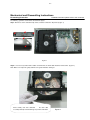
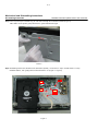
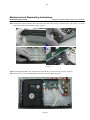
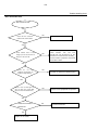
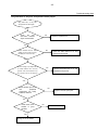
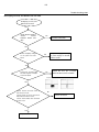
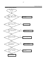
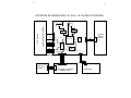
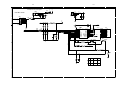
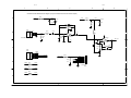
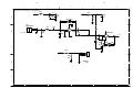
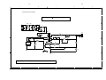
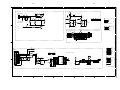
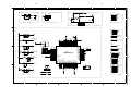
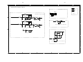
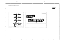
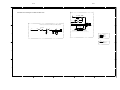
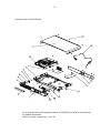
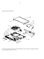
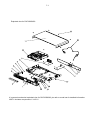
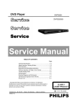
DVP352X(K)
DVP3520/55
DVP3522/55
DVP3520K/93
Service Manual
TABLE OF CONTENTS
Page
. Technical Specifications…………....………………………..............1-2
. Safety Instruction, Warning & Notes….……………………....….....1-3
. Mechanical and Dismantling Instructions…………........................2-1
. Software Upgrades and Region Code Change..............................3-1
. Trouble Shooting Chart………………………………………………. 4-1
. Wiring Diagram………………………………………..………..….….5-1
. Electrical Diagrams and Print-layouts..….…………………....….…6-1
. Set Mechanical Exploded view & Part list.…………………..….….7-1
. Revision List..................................................................................8-1
©Copyright 2010 Philips Consumer Electronics B.V. Eindhoven, The Netherlands
All rights reserved. No part of this publication may be reproduced, stored in aretrieval system or
transmitted, in any form or by any means, electronic, mechanical, photocopying, or otherwise
without the prior permission of Philips.
Published by SL - 009 BU AVM
Version 1.2
Printed in The Netherlands
Subject to modification
CLASS 1
LASER PRODUCT
GB
3141 785 34562
PHILIPS
1-2
1. Technical Specifications, Directions for Use
Index of this chapter:
1.1 Technical Specifications
1.2 Directions for Use
Notes:
• Figures can deviate due to the different set executions.
• Specifications are indicative (subject to change).
1.1
Technical Specifications
For on-line product support please use the following website:
http://www.p4c.philips.com/cgi-bin/dcbint/cpproduct_selector.pl
Here is product information available, as well as getting started,
user manuals, frequently asked questions and software &
drivers.
1.2
Directions for Use
You can download this information from the following websites:
http://www.philips.com/support
http://www.p4c.philips.com
1-3
2. Safety Instructions, Warnings, Notes, and Abbreviation List
•
Index of this chapter:
2.1 Safety Instructions
2.2 Warnings
2.3 Notes
2.4 Abbreviation List
2.1
Safety Instructions
2.3.2
Safety regulations require that after a repair, the set must be
returned in its original condition. Pay in particular attention to
the following points:
• Route the wire trees correctly and fix them with the
mounted cable clamps.
• Check the insulation of the Mains/AC Power lead for
external damage.
• Check the strain relief of the Mains/AC Power cord for
proper function.
• Check the electrical DC resistance between the Mains/AC
Power plug and the secondary side (only for sets that have
a Mains/AC Power isolated power supply):
1. Unplug the Mains/AC Power cord and connect a wire
between the two pins of the Mains/AC Power plug.
2. Set the Mains/AC Power switch to the “on” position
(keep the Mains/AC Power cord unplugged!).
3. Measure the resistance value between the pins of the
Mains/AC Power plug and the metal shielding of the
tuner or the aerial connection on the set. The reading
should be between 4.5 M: and 12 M:.
4. Switch “off” the set, and remove the wire between the
two pins of the Mains/AC Power plug.
• Check the cabinet for defects, to prevent touching of any
inner parts by the customer.
2.2
Warnings
•
•
•
•
All ICs and many other semiconductors are susceptible to
electrostatic discharges (ESD ). Careless handling
during repair can reduce life drastically. Make sure that,
during repair, you are connected with the same potential as
the mass of the set by a wristband with resistance. Keep
components and tools also at this same potential.
Be careful during measurements in the high voltage
section.
Never replace modules or other components while the unit
is switched “on”.
When you align the set, use plastic rather than metal tools.
This will prevent any short circuits and the danger of a
circuit becoming unstable.
2.3
Notes
2.3.1
General
•
Measure the voltages and waveforms with regard to the
chassis (= tuner) ground ( ), or hot ground ( ), depending
on the tested area of circuitry. The voltages and waveforms
shown in the diagrams are indicative. Measure them in the
Service Default Mode (see chapter 5) with a colour bar
signal and stereo sound (L: 3 kHz, R: 1 kHz unless stated
otherwise) and picture carrier at 475.25 MHz for PAL, or
61.25 MHz for NTSC (channel 3).
Schematic Notes
•
Safety regulations require the following during a repair:
• Connect the set to the Mains/AC Power via an isolation
transformer (> 800 VA).
• Replace safety components, indicated by the symbol
,
only by components identical to the original ones. Any
other component substitution (other than original type) may
increase risk of fire or electrical shock hazard.
•
•
•
•
•
2.3.3
Where necessary, measure the waveforms and voltages
with ( ) and without ( ) aerial signal. Measure the
voltages in the power supply section both in normal
operation ( ) and in stand-by ( ). These values are
indicated by means of the appropriate symbols.
All resistor values are in ohms, and the value multiplier is
often used to indicate the decimal point location (e.g. 2K2
indicates 2.2 k:).
Resistor values with no multiplier may be indicated with
either an “E” or an “R” (e.g. 220E or 220R indicates 220 :).
All capacitor values are given in micro-farads (P u10-6),
nano-farads (n u10-9), or pico-farads (p u10-12).
Capacitor values may also use the value multiplier as the
decimal point indication (e.g. 2p2 indicates 2.2 pF).
An “asterisk” (*) indicates component usage varies. Refer
to the diversity tables for the correct values.
The correct component values are listed in the Spare Parts
List. Therefore, always check this list when there is any
doubt.
BGA (Ball Grid Array) ICs
Introduction
For more information on how to handle BGA devices, visit this
URL: www.atyourservice.ce.philips.com (needs subscription,
not available for all regions). After login, select “Magazine”,
then go to “Repair downloads”. Here you will find Information
on how to deal with BGA-ICs.
BGA Temperature Profiles
For BGA-ICs, you must use the correct temperature-profile,
which is coupled to the 12NC. For an overview of these profiles,
visit the website www.atyourservice.ce.philips.com (needs
subscription, but is not available for all regions)
You will find this and more technical information within the
“Magazine”, chapter “Repair downloads”.
For additional questions please contact your local repair help
desk.
2.3.4
Lead-free Soldering
Due to lead-free technology some rules have to be respected
by the workshop during a repair:
• Use only lead-free soldering tin Philips SAC305 with order
code 0622 149 00106. If lead-free solder paste is required,
please contact the manufacturer of your soldering
equipment. In general, use of solder paste within
workshops should be avoided because paste is not easy to
store and to handle.
• Use only adequate solder tools applicable for lead-free
soldering tin. The solder tool must be able:
– To reach a solder-tip temperature of at least 400°C.
– To stabilize the adjusted temperature at the solder-tip.
– To exchange solder-tips for different applications.
• Adjust your solder tool so that a temperature of around
360°C - 380°C is reached and stabilized at the solder joint.
Heating time of the solder-joint should not exceed ~ 4 sec.
Avoid temperatures above 400°C, otherwise wear-out of
tips will increase drastically and flux-fluid will be destroyed.
To avoid wear-out of tips, switch “off” unused equipment or
reduce heat.
• Mix of lead-free soldering tin/parts with leaded soldering
tin/parts is possible but PHILIPS recommends strongly to
avoid mixed regimes. If this cannot be avoided, carefully
clear the solder-joint from old tin and re-solder with new tin.
1-4
Safety Instructions, Warnings, Notes, and Abbreviation List
2.3.5
Alternative BOM identification
It should be noted that on the European Service website,
“Alternative BOM” is referred to as “Design variant”.
The third digit in the serial number (example:
KX 2B0835000001) indicates the number of the alternative
B.O.M. (Bill Of Materials) that has been used for producing the
specific AV set. In general, it is possible that the same AV
model on the market is produced with e.g. two different types
of display, coming from two different suppliers. This
will then result in sets which have the same CTN (Commercial
Type Number; e.g. MCM394/12) but which have a different
B.O.M. number.
Also, it is possible that same model on the market is produced
with two production centers, however their partslist is the same.
In such case, no alternative B.O.M. will be created.
By looking at the third digit of the serial number, one can
identify which B.O.M. is used for the set he is working with.
If the third digit of the serial number contains the number “1”
(example: KX 1B033500001), then the set has been
manufactured according to B.O.M. number 1. If the third digit is
a “2” (example: KX 2B0335000001), then the set has been
produced according to B.O.M. no. 2. This is important for
ordering the correct spare parts!
For the third digit, the numbers 1...9 and the characters A...Z
can be used, so in total: 9 plus 26= 35 different B.O.M.s can be
indicated by the third digit of the serial number.
Identification: The bottom line of a type plate gives a 14-digit
serial number. Digits 1 and 2 refer to the production centre (e.g.
LM is Arts), digit 3 refers to the B.O.M. code, digit 4 refers
to the Service version change code, digits 5 and 6 refer to the
production year, and digits 7 and 8 refer to production week (in
example below it is 2008 week 50). The 6 last digits contain the
serial number.
Model FWM572/12
220-230 50Hz 60W
FWM572/12
LM1A0850005644
2.4
Abbreviation List
0/6/12
2DNR
3DNR
AARA
ACI
ADC
AFC
AGC
AM
ANR
AP
AR
ASF
ATSC
ATV
Auto TV
AV
AVC
AVIP
B/G
BLR
BTSC
Figure 2-1 Serial number (example)
2.3.6
Module Level Repair (MLR) or Component Level Repair
(CLR)
If a board is defective, consult your repair procedure to decide
if the board has to be exchanged or if it should be repaired on
component level.
If your repair procedure says the board should be exchanged
completely, do not solder on the defective board. Otherwise, it
cannot be returned to the O.E.M. supplier for back charging!
2.3.7
Practical Service Precautions
•
•
It makes sense to avoid exposure to electrical shock.
While some sources are expected to have a possible
dangerous impact, others of quite high potential are of
limited current and are sometimes held in less regard.
Always respect voltages. While some may not be
dangerous in themselves, they can cause unexpected
reactions that are best avoided. Before reaching into a
powered TV set, it is best to test the high voltage insulation.
It is easy to do, and is a good service precaution.
B-TXT
C
CEC
CL
CLR
COLUMBUS
ComPair
CP
CSM
CTI
CVBS
DAC
DBE
DDC
SCART switch control signal on A/V
board. 0 = loop through (AUX to TV),
6 = play 16 : 9 format, 12 = play 4 : 3
format
Spatial (2D) Noise Reduction
Temporal (3D) Noise Reduction
Automatic Aspect Ratio Adaptation:
algorithm that adapts aspect ratio to
remove horizontal black bars; keeps
the original aspect ratio
Automatic Channel Installation:
algorithm that installs TV channels
directly from a cable network by
means of a predefined TXT page
Analogue to Digital Converter
Automatic Frequency Control: control
signal used to tune to the correct
frequency
Automatic Gain Control: algorithm that
controls the video input of the feature
box
Amplitude Modulation
Automatic Noise Reduction: one of the
algorithms of Auto TV
Asia Pacific
Aspect Ratio: 4 by 3 or 16 by 9
Auto Screen Fit: algorithm that adapts
aspect ratio to remove horizontal black
bars without discarding video
information
Advanced Television Systems
Committee, the digital TV standard in
the USA
See Auto TV
A hardware and software control
system that measures picture content,
and adapts image parameters in a
dynamic way
External Audio Video
Audio Video Controller
Audio Video Input Processor
Monochrome TV system. Sound
carrier distance is 5.5 MHz
Board-Level Repair
Broadcast Television Standard
Committee. Multiplex FM stereo sound
system, originating from the USA and
used e.g. in LATAM and AP-NTSC
countries
Blue TeleteXT
Centre channel (audio)
Consumer Electronics Control bus:
remote control bus on HDMI
connections
Constant Level: audio output to
connect with an external amplifier
Component Level Repair
COlor LUMinance Baseband
Universal Sub-system
Computer aided rePair
Connected Planet / Copy Protection
Customer Service Mode
Color Transient Improvement:
manipulates steepness of chroma
transients
Composite Video Blanking and
Synchronization
Digital to Analogue Converter
Dynamic Bass Enhancement: extra
low frequency amplification
See “E-DDC”
1-5
Safety Instructions, Warnings, Notes, and Abbreviation List
D/K
DFI
DFU
DMR
DMSD
DNM
DNR
DRAM
DRM
DSP
DST
DTCP
DVB-C
DVB-T
DVD
DVI(-d)
E-DDC
EDID
EEPROM
EMI
EPLD
EU
EXT
FBL
FDS
FDW
FLASH
FM
FPGA
FTV
Gb/s
G-TXT
H
HD
HDD
HDCP
HDMI
HP
I
I2C
I2 D
I2 S
IF
Interlaced
Monochrome TV system. Sound
carrier distance is 6.5 MHz
Dynamic Frame Insertion
Directions For Use: owner's manual
Digital Media Reader: card reader
Digital Multi Standard Decoding
Digital Natural Motion
Digital Noise Reduction: noise
reduction feature of the set
Dynamic RAM
Digital Rights Management
Digital Signal Processing
Dealer Service Tool: special remote
control designed for service
technicians
Digital Transmission Content
Protection; A protocol for protecting
digital audio/video content that is
traversing a high speed serial bus,
such as IEEE-1394
Digital Video Broadcast - Cable
Digital Video Broadcast - Terrestrial
Digital Versatile Disc
Digital Visual Interface (d= digital only)
Enhanced Display Data Channel
(VESA standard for communication
channel and display). Using E-DDC,
the video source can read the EDID
information form the display.
Extended Display Identification Data
(VESA standard)
Electrically Erasable and
Programmable Read Only Memory
Electro Magnetic Interference
Erasable Programmable Logic Device
Europe
EXTernal (source), entering the set by
SCART or by cinches (jacks)
Fast BLanking: DC signal
accompanying RGB signals
Full Dual Screen (same as FDW)
Full Dual Window (same as FDS)
FLASH memory
Field Memory or Frequency
Modulation
Field-Programmable Gate Array
Flat TeleVision
Giga bits per second
Green TeleteXT
H_sync to the module
High Definition
Hard Disk Drive
High-bandwidth Digital Content
Protection: A “key” encoded into the
HDMI/DVI signal that prevents video
data piracy. If a source is HDCP coded
and connected via HDMI/DVI without
the proper HDCP decoding, the
picture is put into a “snow vision” mode
or changed to a low resolution. For
normal content distribution the source
and the display device must be
enabled for HDCP “software key”
decoding.
High Definition Multimedia Interface
HeadPhone
Monochrome TV system. Sound
carrier distance is 6.0 MHz
Inter IC bus
Inter IC Data bus
Inter IC Sound bus
Intermediate Frequency
Scan mode where two fields are used
to form one frame. Each field contains
half the number of the total amount of
IR
IRQ
ITU-656
ITV
JOP
LS
LATAM
LCD
LED
L/L'
LORE
LPL
LS
LVDS
Mbps
M/N
MIPS
MOP
MOSFET
MPEG
MPIF
MUTE
NC
NICAM
NTC
NTSC
NVM
O/C
OSD
OTC
P50
PAL
lines. The fields are written in “pairs”,
causing line flicker.
Infra Red
Interrupt Request
The ITU Radio communication Sector
(ITU-R) is a standards body
subcommittee of the International
Telecommunication Union relating to
radio communication. ITU-656 (a.k.a.
SDI), is a digitized video format used
for broadcast grade video.
Uncompressed digital component or
digital composite signals can be used.
The SDI signal is self-synchronizing,
uses 8 bit or 10 bit data words, and has
a maximum data rate of 270 Mbit/s,
with a minimum bandwidth of 135
MHz.
Institutional TeleVision; TV sets for
hotels, hospitals etc.
Jaguar Output Processor
Last Status; The settings last chosen
by the customer and read and stored
in RAM or in the NVM. They are called
at start-up of the set to configure it
according to the customer's
preferences
Latin America
Liquid Crystal Display
Light Emitting Diode
Monochrome TV system. Sound
carrier distance is 6.5 MHz. L' is Band
I, L is all bands except for Band I
LOcal REgression approximation
noise reduction
LG.Philips LCD (supplier)
Loudspeaker
Low Voltage Differential Signalling
Mega bits per second
Monochrome TV system. Sound
carrier distance is 4.5 MHz
Microprocessor without Interlocked
Pipeline-Stages; A RISC-based
microprocessor
Matrix Output Processor
Metal Oxide Silicon Field Effect
Transistor, switching device
Motion Pictures Experts Group
Multi Platform InterFace
MUTE Line
Not Connected
Near Instantaneous Compounded
Audio Multiplexing. This is a digital
sound system, mainly used in Europe.
Negative Temperature Coefficient,
non-linear resistor
National Television Standard
Committee. Color system mainly used
in North America and Japan. Color
carrier NTSC M/N= 3.579545 MHz,
NTSC 4.43= 4.433619 MHz (this is a
VCR norm, it is not transmitted off-air)
Non-Volatile Memory: IC containing
TV related data such as alignments
Open Circuit
On Screen Display
On screen display Teletext and
Control; also called Artistic (SAA5800)
Project 50: communication protocol
between TV and peripherals
Phase Alternating Line. Color system
mainly used in West Europe (color
carrier= 4.433619 MHz) and South
America (color carrier PAL M=
1-6
Safety Instructions, Warnings, Notes, and Abbreviation List
PCB
PCM
PDP
PFC
PIP
PLL
POR
Progressive Scan
PTC
PWB
PWM
QRC
QTNR
QVCP
RAM
RGB
RC
RC5 / RC6
RESET
ROM
R-TXT
SAM
S/C
SCART
SCL
SCL-F
SD
SDA
SDA-F
SDI
SDRAM
SECAM
SIF
SMPS
SoC
SOG
SOPS
S/PDIF
SRAM
SRP
SSB
STBY
SVGA
SVHS
SW
SWAN
SXGA
TFT
THD
TMDS
TXT
TXT-DW
UI
uP
UXGA
3.575612 MHz and PAL N= 3.582056
MHz)
Printed Circuit Board (same as “PWB”)
Pulse Code Modulation
Plasma Display Panel
Power Factor Corrector (or Preconditioner)
Picture In Picture
Phase Locked Loop. Used for e.g.
FST tuning systems. The customer
can give directly the desired frequency
Power On Reset, signal to reset the uP
Scan mode where all scan lines are
displayed in one frame at the same
time, creating a double vertical
resolution.
Positive Temperature Coefficient,
non-linear resistor
Printed Wiring Board (same as “PCB”)
Pulse Width Modulation
Quasi Resonant Converter
Quality Temporal Noise Reduction
Quality Video Composition Processor
Random Access Memory
Red, Green, and Blue. The primary
color signals for TV. By mixing levels
of R, G, and B, all colors (Y/C) are
reproduced.
Remote Control
Signal protocol from the remote
control receiver
RESET signal
Read Only Memory
Red TeleteXT
Service Alignment Mode
Short Circuit
Syndicat des Constructeurs
d'Appareils Radiorécepteurs et
Téléviseurs
Serial Clock I2C
CLock Signal on Fast I2C bus
Standard Definition
Serial Data I2C
DAta Signal on Fast I2C bus
Serial Digital Interface, see “ITU-656”
Synchronous DRAM
SEequence Couleur Avec Mémoire.
Color system mainly used in France
and East Europe. Color carriers=
4.406250 MHz and 4.250000 MHz
Sound Intermediate Frequency
Switched Mode Power Supply
System on Chip
Sync On Green
Self Oscillating Power Supply
Sony Philips Digital InterFace
Static RAM
Service Reference Protocol
Small Signal Board
STand-BY
800x600 (4:3)
Super Video Home System
Software
Spatial temporal Weighted Averaging
Noise reduction
1280x1024
Thin Film Transistor
Total Harmonic Distortion
Transmission Minimized Differential
Signalling
TeleteXT
Dual Window with TeleteXT
User Interface
Microprocessor
1600x1200 (4:3)
V
VCR
VESA
VGA
VL
VSB
WYSIWYR
WXGA
XTAL
XGA
Y
Y/C
YPbPr
YUV
V-sync to the module
Video Cassette Recorder
Video Electronics Standards
Association
640x480 (4:3)
Variable Level out: processed audio
output toward external amplifier
Vestigial Side Band; modulation
method
What You See Is What You Record:
record selection that follows main
picture and sound
1280x768 (15:9)
Quartz crystal
1024x768 (4:3)
Luminance signal
Luminance (Y) and Chrominance (C)
signal
Component video. Luminance and
scaled color difference signals (B-Y
and R-Y)
Component video
2-1
Mechanical and Dismantling Instructions
Dismantling Instruction
Detailed information please refer to the model set.
The following guidelines show how to dismantle the player.
Step1: Remove 5 screws around the Top Cover, and then remove the Top Cover (Figure 1).
Figure 1
Step2: If it is necessary to dismantle Loader or Front Panel, the Front door should be removed first. (Figure 2)
Note: Make sure to operate gently otherwise the guider would be damaged.
Please kindly note that dismantle
the front door
assembly carefully to avoid damage tray and the front door.
Figure 2
2-2
Mechanical and Dismantling Instructions
Detailed information please refer to the model set.
Dismantling Instruction
Step3: If the tray can’t open in normal way, you can make it through the instruction as below (Figure 3).
Note: Make sure to operate gently otherwise the guider would be damaged.
Figure 3
Step4: Dismantling Front Panel, disconnect the connectors (XS30 1), need release 4 snaps of Front Panel & 2 snaps
of bottom cabinet , then gently pull the Panel out from the set. (Figure 4 - Figure 6)
XP1
XP2
XP3
XP4
XS301
Figure 4
2-3
Mechanical and Dismantling Instructions
Dismantling Instruction
Detailed information please refer to the model set.
Step5: Dismantling Loader, disconnect the 3 connectors (XP2, XP3, XP4) aiming in the below figure, and remove 1 screw that
connects the loader and the bottom cabinet. (Figure 5)
Figure 5
Step6: Dismantling Main Board, first disconnect the connector (XP1), and then remove 4 screws. (Figure 6)
Step7: Remove the 4 screws on Power Board to dismantle the Power Board. (Figure 6)
Figure 6
3-1
Softeware upgrade and region code change
Preparation to upgrade software
1) Power on the set and open the tray, then press "5""5"
B. Read out the software versions to confirm upgrading
on remote control to check the SW File Name.
2) Start the CD Burning software and create a new CD
project (Data Disc) with the following setting:
Label: DVP3XXX (No need the label name)
1)
2)
SW File Name: DVPXXXX_XX.bin
Note: It is required to keep the SW file name accord.
3) Burn the data onto a blank CDR
Power on the set and press "Setup" button on the
remote control.
Press "1""3""7""9" button or press down cursor
on remote control to select "Preferences" and press
right & down cursor to select "Version Info".
The software version and other informations will be
displayed on the TV screen as follows:
Version
XX.XX.XX.XX (Main version)
Sub-Ver
XX.XX.XX.XX (version of applicaton software)
A) Upgrade software via CDR:
8032
XX.XX.XX.XX
1)
Power on the set and insert the prepared Upgrade CDR.
Servo
XX.XX.XX.XX (software version of Servo)
2)
The set will starts reading disc & response with the
RISC
XX.XX.XX.XX
following display TV screen:
DSP
XX.XX.XX.XX
A.
Procedure for software upgrade:
Upgrade file detected
Region Code
X
Upgrade ?
Press PLAY to start
3)
Press "PLAY" button to confirm, then screen will display:
Upgrade file detected
Do not power off
File Copying
4)
Upgrade file detected
Do not power off
Upgrading
The upgraded tray will automatically open when file
copying completed, then take out the disc.
5)
About 1 minute later, the trace will automatically close
when upgrading completed.
B) Upgrade software via USB Flash Drive (only for USB 2.0):
1)
Create the correct software file onto the USB flash drive.
2)
Power on the set and keep no disc, then insert it to the
USB jack of the front panel.
3)
When the DVD player switchs to the USB state automatically,
pls follow the instructions on the TV screen to confrim the
upgrade operation.
Region Code Change
1) Power on the set and open the tray door;
2) Press the "Setup" button on the remote control, then the
setup interface will be displayed on the TV screen;
3) Move the down cursor on remote control to select "Preferences"
and press "1""3""8""9""3""1" on the remote control;
4) Then move the up or down cursor to select the region code.
Note: Restart after above steps.
Caution: The set must not be power off during
upgrading, Otherwise the Main board will be
damaged entirely.
4-1
Trouble shooting chart
Spindle motor does not move
Motor no move
Go
Check the FFC connection
No
Correct connection
between 24P and the loader.
Yes
No
Check whether “M5V”
Check the M5V power supply
(+5V) voltage is normal.
Yes
Check whether laser voltage
No
(1.9V for CD & 2.4V for DVD)
Check/Replace Q103,Q104.
on L101 and L102
Yes
1.Whether voltage on pin102/pin103 of U1
varies between 2.4V and 3.3V (Pin102=3.3V
No
and Pin103=2.4V for CD; Pin102=2.4V and
Pin103=3.3V for DVD),
Check/Replace U1.
2.Whether peripheral components are eroded
or badly soldered.
Yes
Check opu focus
No
1.
Check U1 111pin FOCUS_PWM
signals
2.
If there are F+, F-, T+ and T-
signals output from U10.
Yes
Check/Replace the loader
FOCUS_PWN waveform
4-2
Trouble shooting chart
The power can not be on or off
The power can’t be
on or off
Go
Check the power supply
No
on the power board is
Repair the power board
normal.
Yes
Check if the XS301 on the
front board to XP5 on the
Yes
No
Check/Correct connection
decoder board is in good
contact.
Yes
Whether the connection
No
to K303 is broken.
Correct the connection
Yes
Whether there is 0V and
3.3V voltage difference on
Pin 118 PCON of U1.
Yes
No
Replace U1.
4-3
Trouble shooting chart
All output voltages on the power board is 0V or deviated.
All output voltages on
the power board is 0V or
deviated
Yes
Check whether
Yes
Replace F501
F501 is blown
No
Check whether there is
Replace C501&C502 if D501, D502,
No
D503, D504 are normal.
300V on C501 or C502.
Yes
Check whether 100KHz
oscillating signal on
Pin6 of U1
No
Check/ replace U1.
U1(PIN 3 - RC waveform)
U1(PIN 8 - Drain waveform)
Yes
Check if +5V and +12V
are short.
Yes
Check whether the components in the
short-circuit voltage are defected or eroded.
No
Check whether U1 are eroded.
4-4
Trouble shooting chart
Disc cannot be read.
Disc cannot be read.
Yes
Check the FFC connection
No
Check the loaded circuit
between 24P and the loader.
Yes
1. Whether voltage on pin102/pin103 of U1
Check whether there is laser
voltage (1.9V for CD and 2.4V for
No
varies
between
2.4V
and
3.3V
(Pin102=3.3V and Pin103=2.4V for CD;
Pin102=2.4V and Pin103=3.3V for DVD),
DVD) on L101 and L102.
2.Check whether peripheral components
are eroded or defect
Yes
Check
U1,
U2,
and
No
peripheral components are
Re-solder or replace the defective parts
eroded or badly soldered.
Yes
Check if there is RFO signal on
pin17 of XP2. (The normal RFO
No
Check U1 and peripheral components
signal is a clear reticulated wave)
Yes
Check the connection
between U1
Yes
Replace U1 or loader.
No
Correct connection
4-5
Trouble shooting chart
Only DVD disc or only disc except DVD can be played
Only DVD disc, or only disc
except DVD can be Played.
Go
Check
the
FFC
connection between
24pin and the loader.
No
Check the loaded circuit
Yes
Check whether there is laser
No
voltage (1.9V for CD and 2.4V
Check the solder status on U1 and
peripheral components
for DVD) on L101 and L102.
Yes
Whether voltage on pin102/pin103 of
No
U1 varies between 2.4V and 3.3V
check if bad solder exist on U1 and
peripheral components
(Pin102 =3.3V and Pin103=2.4V for
CD; Pin102=2.4V and Pin103=3.3V
Yes
Check whether pins of U1
and
peripheral
components are badly
soldered, defected
No
Replace the bad spare parts
Yes
Check Q103, Q104
whether in good
condition
Yes
Change U1 or the loader.
No
Correct connection
4-6
Trouble shooting chart
No display on LED, and buttons do not work
No display on LED, and
buttons do not work
Yes
Check whether there is
correct
contact
between XS301 and
XP5
No
Correct connection
Yes
Check VCC(M5V) voltage
on the power and front
Fix power supply board top
a power supply for should
electric circuit
No
board
Yes
Check there are STB, SDA
and SCK signals on XS301
No
Check the U1’s pin 1,119,122
arrive the XP5 connect condition
on the front board.
XP5 (PIN 1 CLK)
XP5 (PIN3 DOUT)
Yes
1.Check whether bad solder exists on
U301 and pins of LED,
2.Check whether the circuit connected to
K302, K303 and K301 is broken,
3.Check whether R300, R301 and R302
are open-circuit.
Yes
Replace U301 or LED
No
Correct connection
4-7
Trouble shooting chart
Distorted audio and loud noise
Distorted audio and
loud noise
Yes
Check the power supply
voltages M5V to the
operation amplifying Q544
is normal.
No
Check Q544
Yes
Check whether the muting
No
resistance R369,R375 are
Replace R369,R375
normal
Yes
Check whether the muting
transistor Q361,Q362 are
normal
No
Replace Q361,Q362
Yes
Checking the U361 leads
No
&RUUHFWFRQQHFWLRQ
the feet has no to break to
open
Yes
Check the voltage on pin3
or pin5 of U361 is OK.
No
Replace R362,R363
(Should be 2.5~3.1V)
Yes
Check whether the U1
or U361 powersupply
normal
Yes
Replace U1 or U361
No
Check U361
4-8
Trouble shooting chart
Abnormal color of video picture
Abnormal color of
video picture
Yes
Check
whether
the
No
Check Y1, R10,R11,C10 and C11
27MHz output signal
Yes
Check whether the 3.3V
and 1.2V power supply
voltages on the decoder
board are normal.
No
Check other of power supply electric
circuit
Yes
Check whether the
video filter network
circuit is normal.
No
Correct the connection
Yes
Check if the video signals on Pin
69,73,74,75, of U1 are normal
No
change U1
4-9
Trouble shooting chart
Remote reception is insensitive or fails.
Remote reception is
insensitive or fails.
Go
Check if the remote
control works properly.
No
Check battery
Yes
Check if the power
supply voltage to the
remote censor is normal
No
Check
R315ǃC315
Yes
Use an oscilloscope to check if
No
there is output waveform from the
first pin IR of the remote censor
REM301(PIN1 - RC waveform)
after pressing button on the remote
control.
Yes
Check if there is IR
signal on pin 2 of U1
Yes
Change U1
IR waveform
No
Correct connection
4-10
Trouble shooting chart
No video picture, no sound.
No video picture,
no sound.
No
Check whether all the voltages
CVBS(R21 point) waveform
Check the loaded circuit
from the power board to the
decoder board are normal.
Yes
Check if the reset circuit consisting of
No
CE2, D1,Q1 is normal (at a low level
for
tens
of
milliseconds,
then
Change CE2, D1,Q1.
constantly at 3.3V).
27Mhz waveform
Yes
Check whether there is
Crystal oscillator Y1 and
No
peripheral components
27MHz signal output.
are defected or eroded.
Yes
Check if there is 135MHz
No
Check whether
short-circuit or bad
solder on U176,U186
signal output on R193.
SDRAM(R193 DCLK) waveform
No
Yes
Check if short-circuit and
bad solder exist on Pin
69
No
Check U1.
Yes
Yes
Reconnect the component in
5-1
5-1
5
4
3
2
1
SPHE8202R-D(2ch) WIRING DIAGRAM
D
D
Pr
Y
P1
Pb
CVBS
COAX
FR
FL
AUDIO
AMP&LPF
MOTER
DRIVER
16MІ㸠
FLASH
EN25T16
1
5PIN*2.0
6PIN*2.0
5
XP1
1
4PIN*2.0
6
4
XP7
1
B
5V
IR
GND
DATA
STB
CLK
MAIN BOARD
B
AM5888
5
6
LOADLOAD+
OUTSW
GND
INSW
C
XS201
5PIN*2.5
1
6PIN*2.0
XP8
SPSP+
HOMESW
GND
SLSL+
GND
+P12V
GND
M+5V
M+5V
XP2
SPHE8202R-D
24
1
POWER
SUPPLY
TNY176
1
5
ISSI
64M
SDRAM
XP4
24PIN*0.5
5PIN*2.5
VIDEO LPF
1
XP9
C
TDM-3 LOADER+IM S76RFXP2
DVD LOADER
P4
+5V
GND
USB_DM
USB_DP
6
XP303
4
4
KS6S
KEY2
LED+
LED-
SWITCH
4PIN*2.0
BOARD
1
1
XS302
4
XS301 6PIN*2.0
1
XS601
4PIN*2.0
4PIN*2.0
1
LED DISPLAY+ET6202
(LED229GA3JY)
USB
A
A
Remark: DVP3520 no USB output.
5
4
3
2
1
5-1
5-1
DVP3520K SPHE8202RQ-D(2ch) WIRING DIAGRAM
TDM-3 LOADER+IM S76RFXP2
Pr
Y
P1
Pb
CVBS
COAX
FR
FL
AUDIO
AMP&LPF
MOTER
DRIVER
AM5888
5
6
LOADLOAD+
OUTSW
GND
INSW
16MІ㸠
FLASH
EN25T16
1
5PIN*2.0
6PIN*2.0
5
1
XP1
1
6
3PIN*2.0
XP476
MIC
6
4
4
KS6S
KEY2
LED+
LED-
SWITCH
4PIN*2.0
BOARD
1
3
5V
IR
GND
DATA
STB
CLK
MAIN BOARD
XP303
1
XS302
XS301 6PIN*2.0
+12VA
GND
3
1
XP601
3PIN*2.0
4PIN*2.0
1
XS201
3PIN*2.5
1
6PIN*2.0
XP8
SPSP+
HOMESW
GND
SLSL+
24
1
+P12V
GND
M+5V
XP2
SPHE8202RQ-D
POWER
SUPPLY
TNY176
1
5
ISSI
64M
SDRAM
XP4
24PIN*0.5
3PIN*2.5
VIDEO LPF
1
XP9
DVD LOADER
P4
LED DISPLAY+ET6202
(LED229GA3JY)
KARAOKE
6-1
6-1
5
4
3
Front Board Circuit Diagram:
VCC
2
1
U5V
R315
REM301
5
)5200$,1%2$5'
4
5
4
VCC
GND
IR
3
2
1
100 ohm R318
100R/NC
IR
+
REM
for dvp352x
IR
VCC
GND
DATA
CS
CLK
U5V
1
2
3
4
5
6
7
8
9
10
C306
0.1u
C315
47p
XS301
D
R320
VCC
0R
1
2
3
4
LED+
LEDPOWER_K1
POWER_K
U5V
STB_LED
XS302
CON4(2.0)
CE301
47uF
C316
100p
IR
DATA
CS
CLK
C307
100p
D
C308
100p
VCC
POWER_K
STB_LED
5VL
R303 R304 R305
R319
0 ohm
LED-
CON10(2.0)
R306
4K7
DATA
CLK
CS
R300
R301
R302
4K7
51K
4K7
100
100
100
R307
R308
10K
10K
C300 C301 C302
C
100P 100P
R317 33R
R309
R310
5VL
0.1u
1
2
3
4
5
6
7
8
9
10
11
12
13
14
1K
1K
SEG1
SEG2
SEG3
SEG4
SEG5
SEG6
100P
C303
U301
ET6202
CE300
+
OSC
DI/O
CLK
STB
KEY1
KEY2
VDD
SEG1/KS1
SEG2/KS2
SEG3/KS3
SEG4/KS4
SEG5/KS5
SEG6/KS6
SEG7/KS7
LED1
GRID[1:7]
GND
GRID1
GRID2
GND
GRID3
GRID4
GND
VDD
SEG14/GRID5
SEG13/GRID6
SEG12/GRID7
SEG10/KS10
SEG9/KS9
SEG8/KS8
28
27
26
25
24
23
22
21
20
19
18
17
16
15
GRID1
GRID2
GRID3
GRID4
GRID5
GRID6
GRID7
SEG1
SEG2
SEG3
SEG4
SEG5
SEG6
GRID1
GRID2
GRID3
GRID4
VCC
GRID7
GRID6
GRID5
LED+
R316 33R
1
2
3
4
5
6
7
8
9
10
11
12
13
GRID1
GRID2
GRID3
GRID4
GRID5
GRID6
GRID7
SEG1
SEG2
SEG3
SEG4
SEG5
SEG6
C
JDD350501AG
47uF
SEG[1:6]
KEY1
KEY2
K301
1N4148
D301
1N4148
D302
R312
K302
open/close
play/pause
1K
R311
1K
KS2
POWER_K
R313
0R
POWER_K1
B
B
R314
0R/NC
R311
C304
100p
R313
R314
C305
100p
0.3W
N
N
Y
1W
Y
Y
N
A
A
5
4
3
2
1
6-2
6-2
A
B
C
D
E
Switch Board Circuit Diagram:
1
1
K303
1
2
3
4
2
POWER
2
LED3
XP1
CON4(2.0)
C319
47p
SWITCH
C317
47p
C318
47p
BOARD
3
3
4
4
A
B
C
D
E
6-3
6-3
1
2
3
4
5
OK Board & USB Board Electric Diagram (Only for DVP3522 and has not karaoke output)
12V
R210
12VA
150
CE201
22uF
C201
REF
22K
0.1u
A
CE200
22uF
R203
22K
C205
47p
R205
180K
R211
C203
U200A
B
C211
100K
1
NJM4558
2.2uF
1000p
REF
12VA
C208
100p
5
+
6
-
C204
100p
R206
C
20K
P600
USB
47-USB003-XX2
USB
1
2
3
4
5
6
MGND
MGND
VCC
SGND
MGND
L200
USB_DN
USB_DP
L201
U200B
R207
100K
C206
47p
C
R208
MIC_OUT
MIC
12V
1K
VCC
SGND
USB_DN
USB_DP
680
1
2
3
4
5
6
7
D
AGND
500Z
MGND
MIC_OUT
C209
2.2uF
R209
D
NJM4558
7
4
ĭ3.5mm
3
8
R200
10K
2.2uF
2
8
5.6K
4
R201
1
2
3
C210
+
KARAOKE
B
47-EAR024-XX0
P601
KARAOKE INPUT
R202
12VA
-
A
8PIN/2.0mm
XP601
AGND
500Z
MGND
L202
SGND
500Z
E
E
1
2
3
4
5
7-3
7-3
1
2
3
4
5
OK Board Circuit Diagram for DVP3520K/93:
R210
12VA
150
CE201
A
22uF
R202
REF
22K
0.1u
CE200
A
22uF
R203
22K
C205
47p
R205
180K
R211
3
C203
U5A
100K
1
2.2uF
NJM4558 OPA
CE202
1000p
REF
C211
12VA
C208
100p
10uF
8
R200
10K
2.2uF
2
NJM4558 OPA
5
+
6
7
4
5.6K
4
R201
1
2
3
C210
8
ĭ3.5mm
C201
+
KARAOKE
B
47-EAR024-XX0
P601
KARAOKE INPUT
12VA
-
12V
C204
100p
B
MIC_OUT
U5B
R206
R207
100K
20K
C206
47p
C209
2.2uF
C
C
R208
MIC_OUT
MIC
12V
1K
1
2
3
R209
680
D
D
8PIN/2.0mm
XP601
E
E
1
2
3
4
5
6-4
6-4
A
B
C
D
E
Power Board Circuit Diagram:
1
1
* CAUTION :
THE PARTS MARKED WITH
ARE IMPORTANT PARTS ON THE SAFETY.
PLEASE USE THE PARTS HAVING THE DESIGNATED PARTS NUMBER WITHOUT FAIL.
F501
T2AL/250ac
TR501
NTC 10
1
P501
+
RV501
+
+
2
2
CX501
CON502
10K471
AC INPUT
D502
1N4007
L501
680uH
0.1uF/275Vac
C501 +
D504 (10uF)22uF/400V(250V)
C502 +
1N4007
(10uF)22uF/400V(250V)
D503
1N4007
1
1
AC INPUT
1
+
AC INPUT
CN501
D501
1N4007
L503
20mH
P502
2
FB501
FB
7
2
T501
6
CON503
C504
152/1KV
R502
R503
1/4W120K 1/4W120K
FR102
4
D507
IN4007
R15
D506
5
8
1/6W 10K
10
3
+
C509
10uF/16V
+
C512
10uF/50V
D508
FR102
C513
0.1uF/63V
+
D509
L502
6.8uH
1
9
EN/UV
C507
2200uF/10V
+
C508
470uF/16V
R505
1/6W12K 1%
R509
1/6W100
1/6W100k
1
R513
4
S
S
7
S
6
S
5
3
8
2
NC
BP/M
4
Drain
3
+
U1
TNY177PN
1/6W10k
SR360
11
1
C505
GND
+12V
GND
+5V
+5V
5X2.5 HEADER
2
R5061/6W 680
R504
47uF/25V
R516
1/6W10k
5
4
3
2
1
R508
1/6W1k
R510
1/6W10k
3
C511
0.1uF/63V
3
2
3
U502
PC123X92
1
R507
1/6W11.3k 1%
2
U503
AZ431
CY501
102/400Vac
4
4
* No use the Class 1 environment management materials of SS-00259
* All of moulding resinous, ink, paint and coating electric wire must be ordered from designated GP supplier of Philips.
A
B
C
D
E
6-5
6-5
A
B
C
D
E
Main Board Circuit Diagram: POWER & MOTOR DRIVER
TO POWER BOARD
1.8/2W
M5V
GND
C753
1uF
GND
Q753
SS8550D
50mA
C752
0.1uF
C751
0.1uF
R752
+12V: +12V(+-10%)
R753
NM/0
Q761
4.7K
R757
REG01
R766
12K 1%
10K
1
Q762
SS8550D
b
R767
DV18
R765
20K 1%
R758
8202RᮍḜ⫼4.7K.
DV33
TR_B2
DV33
SS8550D
SS8550D
4.7K
R762 10/1W
TR_B1
+12V
2.2K
Q751
R755
+5V: +5V(+-2.5%)
Inor=155mA
Istandby:8mA
Imax=???mA
+5V
e
1
R761
Inor=360mA
1
2
3
4
5
NM/0
M5V
c
XP1
5pin/2.5mm
R751
Inor=520mA
Istandby:30mA
5V
M5V
4.7k
5.1k
1.825~1.849V
1.875~1.90V
R767
0
+
C761
0.1uF
REG02
CE761
220uF16V
USB_CON
C762
modify
IR
VSDA
VSTB
VSCK
+ CE762
0.1uF
R768
NC
IR
VSDA
VSTB
VSCK
220uF16V
Vref = 1.235--1.27V
R754
PCON:
L: STBY
H: Working
4.7K
PCON
R756
1K
Q752
GND
PCON
POWER_K
WAKE_SW
GND
BT3904
PCON
POWER_K
WAKE_SW
USB_CON
USB_CON
DV33
R84
4.7K
WAKE_SW
IR
2
R87
470NC
R80
100
R88
R89
100
100
100
M5V
5V
R81
R82
R83
VSDA
VSTB
VSCK
POWER_K
PCON
R86
R85
XP5
11
10
9
8
7
6
5
4
3
2
1
DV33
0
0/NC
470/NC
470NC
LED-
9.IR
8.M5V
7.GND
6.DATA
5.CS
4.CLK
2
11PIN/2mm
C84
+CE176
220uF16V
C86
C80
C81
C82 C87
C83
C85 0.1u
100pF/NC
100pF 100pF 100pF
100pF/NC100pF 100pF/NC
TO FRONT PANEL
SP+
SPM+
C102
25
26
1000pF
LD-DVD
5V_HFM
MDI
LD-CD
VR_DVD
VR_CD
L102
R111
L101
10uH
SP-A
LDSW R130
For SUNPLUS Platforms.
0 TRCLOSE
5V_OPU
VREF_OPU
R135
0.1uF
C113
0.1uF
C103
LDSW
D
C
TT+
F+
F-
R123
10K
C100
0.1uF
FMSO
TRSO
DMSO
FOSO
M_BIAS
STBY
TRIN
TROUT
LIMIT
3
10uH
5V
E
F
B
A
RFO
SPM-
NM/0
DV33
U10
2.2
Q103
SS8550
+ CE100
100uF16V
T+
TSLSL+
M5V
LDO_DVD
CE101
RFV33
R106
5.1
R107
5.1
47uF16V
Q104
SS8550
FMSO
C111
0.1uF
+ CE102
27
28
TOP
1
2
3
4
5
6
7
8
9
10
11
12
13
14
15
16
17
18
19
20
21
22
23
24
TROPEN
FMSO
TRSO
DMSO
FOSO
M_BIAS
STBY
TRIN
TROUT
LIMIT
C101
+
3
TROPEN
1000pF
XP2
SMD0.5 TOP
XOPVIP
XOPVIN
47uF16V
LDO_CD
CE104
100uF16V
+
C105
0.1uF
TR_B2
TRSO
M_BIAS
STBY
R112
10K
0.1uF
C106
15
16
17
18
19
20
21
VOTK+
VOTKVOLD+
VOLDVCC2
NC
VCTL
30
G2
22
23
24
25
26
27
28
GND
VINLD
NC
TRB2
VINTK
BIAS
MUTE
VOFC+
VOFCVOSLVOSL+
VOTR+
VOTRVCC
14
13
12
11
10
9
8
G1
29
REV
FWD
REGO1
VINSL+
REGO2
TRB1
VINFC
7
6
5
4
3
2
1
F+
FSPM+
SPMLOAD+
LOAD-
TRCLOSE
TROPEN
REG01
DMSO
REG02
TR_B1
FOSO
MOTOR I/F
DV33
M5V
R114
10K/NC
LIMIT
C107
0.1uF/NC
R134
10K
SP-A
SP+
GND
SLSL+
1
2
3
4
5
6
1
2
3
4
5
XP4
XP3 5PIN/2mm
6PIN/2.0mm
GND
TRAY_DECO
C109
100pF/NC
R116
10K
LOAD-
R118
1K
R119
2.2K
A
B
C
D
E
F
RFO
VREF_OPU
LDO_CD
LDO_DVD
LDSW
MDI
C110
LOAD+ 0.1UF
TROUT
TRIN
C108
100pF/NC
VR_DVD
VR_CD
DMSO:SPINDLE MOTO
FMSO:FEED MOTO,i.e Sledge motor
AM5888
TRSO:Track error
A
B
C
D
E
F
RFO
VREF_OPU
LDO_CD
LDO_DVD
LDSW
MDI
VR_DVD
VR_CD
OPU I/F
FOSO:Focus error
4
4
A
B
C
D
E
6-6
6-6
A
B
C
D
Main Board Circuit Diagram: SPHD8202R-D
E
modify
DV33
R5
Crystal
R10
4.7K
M5V
Y1
XI
C11
33pF
33
R11
XO
33pF
GND
C12
C251 C252
NM/15pF
1
100pF 100pF
Put these Compnonents as
closer as possible to
MT1389
0
M_D[0..15]
TP11
10k
R7
R2
C253
100pF
FV33
R3
CE2
10uF16V
+
1
2
3
4
TXD
RXD
C10
27MHz
XP8
4pin/2.0mm
100
URST#
URST#
1K
C1
0.1uF
R1
10K
1N4148
MA[0..11]
M_DQM[0..1]
M_BA[0..1]
Q1
2N3904
D1
DQ[0..15]
M_A[0..11]
For all Sunplus Platforms.
SP8202R
SP8203R
47
OPEN
R5
0
OPEN
DCLK
RAS#
CAS#
WE#
SPI_CLK
SPI_CE
SPI_D1
SPI_D0
DV33
SF_CK
SF_CS
SF_DI
SF_DO
SF_WP
Digital
SD33
CE25 47uF16V
C36
CDLDO
DVDMDI
CDMDI
0.1uF
Close to 8202R-D
CE26 47uF16V
R20
10
AD_VCC3
CE22
C30
10uF16V
0.1uF
Internal AD +3.3V
RF3.3V
C37
0.1uF
C38
C39
1000pF
1000pF
TRSO
FOSO
0.1uF
0.1uF
DMSO
FMSO
C40
C41
VREF_OPU
M_BIAS
R34
RFDA3.3V
R25
Close to 8202RX-D
3
TRIN
TROUT
Play 90mA
Standby 8mA
FB22
FB500R
C31 C32
VSTB
CDVR
SPI_CE
SPI_D0
SPI_CLK
SPI_D1
TROPEN
Video DAC +3.3V
0.1uF0.1uF
47uF16V
2.2
C33
470uF6.3V 0.1uF
Internal DA +3.3V
R42
4.7k
POWER_K
WAKE_SW
VCC1.2
C34
C35
C48
0.1uF
0.1uF
0.1uF
VR_CD
R35
0
CDVR
VR_DVD
R36
0
DVDVR
Close to 8202RX-D
4
A
VVCC3
V_CVBS
V_FSADJ
V_COMP
SPHE8202RX-D-128
AVCC3
DAC_VREF
CE27
C43
10uF16V
IR
VSDA
VSTB
VSCK
0.1uF
IR
VSDA
VSTB
VSCK
FRONT PANEL CONTROL I/F
AKIN1
USB & KOK & OTHER I/F
AD_VCC3
USB_CON
USB_DP
USB_DM
AKIN1
PCON
POWER_K
WAKE_SW
AUDIO_MUTE
SPDIF
M_A3
M_A2
M_A1
M_A0
M_A10
M_BA1
M_BA0
M_RAS
M_CAS
M_WE
M_DQM0
M_A4
USB_CON
USB_DP
USB_DM
AKIN1
PCON
POWER_K
WAKE_SW
A
B
C
D
E
F
RFO
VREF_OPU
CDLDO
DVDLDO
LDSW
DVDMDI
3
A
B
C
D
E
F
RFO
VREF_OPU
LDO_CD
LDO_DVD
LDSW
MDI
OPU I/F
R41
4.7k
0
U1
64
63
62
61
60
59
58
57
56
55
54
53
52
51
50
49
48
47
46
45
44
43
42
41
40
39
DV33
DV18
R23
ADAC_AVSS
ADAC_AVDD
ADAC_AVDD
VREF
AOUT_LS
AOUT_RS
ADAC_AVSS
AOUT_SUBW
AOUT_CENTER
AIN_R
AD_AVDD
AD_AVSS
GPIO29
SPDIF_OUT
M_A3
M_A2
M_A1
M_A0
M_A10
M_BA1/GPIO27
M_BA0
M_RAS
M_CAS
M_WE
M_DQM0
M_A4
AUDIO_MUTE
SPDIF
AUDIO I/F
1
2
3
4
5
6
7
8
9
10
11
12
13
14
15
16
17
18
19
20
21
22
23
24
25
26
27
28
29
30
31
32
33
34
35
36
37
38
AVCC3
CE24
68K
CDLDO
DVDMDI
CDMDI
SRV_AVDD
V21
V165
DA_AVSS
DA_TEO
DA_FEO
DA_AVDD
SPDC_OUT
SC_OUT
DVDVR
DMEA
SD_D1/GPIO4
SD_D0/GPIO5
SD_CLK/GPIO6
TRAYIN/SD_SMD/GPIO7
TRAYOUT/SD_D3/GPIO8
SD_D2/GPIO9
CDVR
SPI_CE
SPI_D0
SPI_CLK
SPI_D1
TRAY+
VSDA
IR
R21
20K
R24
2.2K
2.2K
DVDVR
STBY
POWER_K
PCON
VSCK
VVCC3
CE23
R33
103
104
105
106
107
108
109
110
111
112
113
114
115
116
117
118
119
120
121
122
123
124
125
126
127
128
B
R40
100
GPIO25
M_A9
M_A8
M_A7
M_A6
M_A5
RF +3.3V
DVCC3
0.1uF
2
AL
AR
AUDIO_MUTE
SPDIF
SP+
R37
TROPEN
FMSO
TRSO
DMSO
FOSO
M_BIAS
STBY
TRIN
TROUT
LIMIT
VR_CD
VR_DVD
XOPVIN
XOPVIP
1
XOPVIP
XOPVIN
R30
0
M_A11
0.1uF
0.1uF
WAKE_SW
TXD
M_D0
M_D1
M_D2
M_D3
M_D4
M_D5
M_D6
M_D7
M_D15
M_D14
M_D13
M_D12
M_D11
M_D10
M_D9
M_D8
M_DQM1
100uF16V
AL
AR
102
101
100
99
98
97
96
95
94
93
92
91
90
89
88
87
86
85
84
83
82
81
80
79
78
77
76
75
74
73
72
71
70
69
68
67
66
65
0.1uF
Close to 8202RX-D
VCC1.2
C28
AR
RXD
C27
URST#
CE21
C44
V_R/V
V_B/U
V_G/Y
DVDLDO
FB500R
V_R/V
V_B/U
V_G/Y
V_CVBS
VIDEO I/F
AL
XOPVIN
XOPVIP
E
F
A
B
C
D
RFO
RFDA3.3V
RF3.3VFB23
RF3.3V
FB500R
CE28
47uF16V
DVDLDO
APC_AVSS
OPVIN
OPVIP
CDE
CDF
DVDA
DVDB
DVDC
DVDD
RFIS
AGCCAP
AD_AVDD
AD_AVSS
LDSW/GPIO40
HOME/GPIO39
VDD_18
CLKOUT
CLKIN
PLL_VDD
PLL_VSS
USB_AVSS
USB_DM
USB_DP
USB_AVDD
VDD_18
TV_AVSS
TV_DAC3
TV_DAC2
TV_DAC1
TV_AVDD
TV_AVSS
TV_AVDD
TV_DAC0
V_FSADJ
V_COMP
AOUT_R
AOUT_L
RFV33
C29
FB21
DVCC3
VCC1.2
VFD_CLK/GPIO16
VFD_STB/GPIO17
VFD_DATA/GPIO18
VDD_33
RESET_B
VSS
IR/GPIO19
GPIO20
GPIO21
VDD_18
M_DQM2/GPIO22
M_DQM3/GPIO23
M_D0
M_D1
M_D2
M_D3
M_D4
M_D5
M_D6
M_D7
M_D15
M_D14
M_D13
M_D12
M_D11
M_D10
M_D9
M_D8
M_DQM1
VSS
M_CLK
VDD_33
M_A11/GPIO25
M_A9
M_A8
M_A7
M_A6
M_A5
RFV33
0.1uF
DVCC3
C45
1uF
C23
Close to SDRAM
VCC1.2
VVCC3
SDRAM +3.3V
FB500R
DVCC3
FB20
R32
4.7K
RF3.3V
Close to 8202RX-D
V_R/V
V_B/U
V_G/Y
V_CVBS
R31
1K
RAM_CLK
2
VVCC3
RF3.3V
USB_DM
USB_DP
C24
XO
XI
C22
LDSW
LIMIT
C21
0.1uF 0.1uF 0.1uF 0.1uF
SF_WP
SPI FLASH I/F
DVCC3
C20
1
DRAM I/F
For SUNPLUS8202R/03R
R4
DQM[0..1]
BA[0..1]
RAM_CLK
M_RAS
M_CAS
M_WE
C
TROPEN
FMSO
TRSO
DMSO
FOSO
M_BIAS
STBY
TRIN
TROUT
LIMIT
VR_CD
VR_DVD
XOPVIN
XOPVIP
MOTOR I/F
4
D
E
6-7
6-7
A
B
C
D
E
Main Board Circuit Diagram: SDRAM&FLASH
1
1
SD33
+CE186
47uF16V
C186
C187
C188
0.1uF
0.1uF
0.1uF
C189
0.1uF
platform
89S
R194
Open
Close
R195
Open
Close
R186
Close
Open
R192
Close
Open
DQ[0..15]
DQ[0..15]
Not 89S
MA[0..11]
BA[0..1]
DQM[0..1]
DCLK
CAS#
RAS#
WE#
CAS#
RAS#
WE#
SD33
MA[0..11]
BA[0..1]
DQM[0..1]
DCLK
U186
U187 ESMT M12L16161A-7
DRAM
2
MA0
MA1
MA2
MA3
MA4
MA5
MA6
MA7
MA8
MA9
MA10
DBA0
21
22
23
24
27
28
29
30
31
32
20
19
A0
A1
A2
A3
A4
A5
A6
A7
A8
A9
A10
BA/A11
SDCLK
SDCKE
35
34
CLK
CKE
DCS#
DRAS#
DCAS#
DWE#
18
17
16
15
CS
RAS
CAS
WE
DQM0
DQM1
14
36
DQML
DQMH
33
37
26
50
NC
NC
VSS
VSS
DQ0
DQ1
DQ2
DQ3
DQ4
DQ5
DQ6
DQ7
DQ8
DQ9
DQ10
DQ11
DQ12
DQ13
DQ14
DQ15
2
3
5
6
8
9
11
12
39
40
42
43
45
46
48
49
VCC
VCC
1
25
VCCQ
VCCQ
VCCQ
VCCQ
7
13
38
44
VSSQ
VSSQ
VSSQ
VSSQ
4
10
41
47
DQ0
DQ1
DQ2
DQ3
DQ4
DQ5
DQ6
DQ7
DQ8
DQ9
DQ10
DQ11
DQ12
DQ13
DQ14
DQ15
SD33
SD33
MA0
MA1
MA2
MA3
MA4
MA5
MA6
MA7
MA8
MA9
MA10
MA11
DBA0
DBA1
23
24
25
26
29
30
31
32
33
34
22
35
20
21
A0
A1
A2
A3
A4
A5
A6
A7
A8
A9
A10/AP
A11
BA0/A13
BA1/A12
SDCLK
SDCKE
38
37
CLK
CKE
DCS#
DRAS#
DCAS#
DWE#
19
18
17
16
CS
RAS
CAS
WE
DQM0
DQM1
15
39
DQML
DQMH
36
40
NC
NC
54
41
28
VSS
VSS
VSS
DQ0
DQ1
DQ2
DQ3
DQ4
DQ5
DQ6
DQ7
DQ8
DQ9
DQ10
DQ11
DQ12
DQ13
DQ14
DQ15
2
4
5
7
8
10
11
13
42
44
45
47
48
50
51
53
VCC
VCC
VCC
1
14
27
VCCQ
VCCQ
VCCQ
VCCQ
3
9
43
49
VSSQ
VSSQ
VSSQ
VSSQ
6
12
46
52
DQ0
DQ1
DQ2
DQ3
DQ4
DQ5
DQ6
DQ7
DQ8
DQ9
DQ10
DQ11
DQ12
DQ13
DQ14
DQ15
SDCKE
DCS#
DRAS#
DCAS#
DWE#
SF_CK
SF_CS
SF_DI
SF_DO
SF_WP
RAS#
CAS#
WE#
DBA0
DBA1
SF_CK
SF_CS
SF_DI
SF_DO
SF_WP
S-FLASH
BA0
BA1
SD33
SD33
SDCLK
R193
33
DCLK
2
C190
10pF
8202RᮍḜ⫼10pF.
ESMT M12L64164A-7T
SDRAM64M
If the Main chip is 89S must use Resistor R186 and R192 or use R194 and R195.
FV33
R182
R186 10K
10K
SF_CS
SF_DO
SF_WP
3
1
2
3
4
R183
R184
10K
U176
AT25FS040/EN25B80
CE# VDD
SO HOLD#
WP# SCK
VSS
SI
8
7
6
5
SF_DI
R185 SF_CK
0R
3
C176
0.1uF
4M/8M/16M bits
10K/NC
Note 2:IF use R183,Must take over R181.Default use R183(10K),and R181 Open.
4
4
A
B
C
D
E
6-8
6-8
A
B
C
D
E
Main Board Circuit Diagram: AUDIO I/F
AR
AL
AR
AL
For 6CH and without optical output model
AUDIO_MUTE
SPDIF
1
AUDIO_MUTE
SPDIF
1
P441
27K 1%
R366
C365
6CH Audio AMP for single input SUNPLUS.
120pF
C441
47pF/NM
C443
1000pF
5
4
3
2
1
47-RCA193-XX1
COAXIAL
RCH
LCH
RCA
RCA/AUDIO OUT
AUDIO I/F
C442
1000pF
4
01UAUIFTN-401
R365
4.7K 1%
C362
REFA
0.1uF
6
5
1500pF
C631
+12VA
0.1uF
CE363
7
R368
10uF16V
U361B
LM4558
8
C364
+
10K 1%
+
R364
-
AL
470
LCH
R367
10K A_MUTE R369
470
+12VA
Q361
2N3904
Audio Ampifier Circuit.
R372
SPDIF
27K 1%
C367
R451
C452
100
R452
100
120pF
0.1uF
COAXIAL
C451
100pF
4.7K 1%
C363
CE364
4
R371
10K 1%
0.1uF
REFA
3
1
1500pF
2
10uF16V
R374
470
RCH
Output Interface Circiut for SPDIF Coaxial.
U361A
LM4558
8
C366
2
+
R370
+
AR
-
2
R373
10K
+12VA
A_MUTE
R375
470
Q362
2N3904
Audio Ampifier Circuit.
+12VA
+12V
R361
100
+12VA
+
R362
CE361
100uF25V
36K
REFA
R363
10K
+ CE362
M5V
100uF16V
Q544
A_MUTE
9012
R548
POWER Ciucuit of OP AMP
R550
4.7K
4.7K
R549
3
10K
R547
CE541 +
3.3K
AUDIO_MUTE R545
4.7K
3
Q545
9012
220uF16V
Q543
2N3904
R546
22K
POP Noise Cancel Circuit For Power On and Power Off.
4
4
A
B
C
D
E
6-9
6-9
5
4
3
2
1
Main Board Circuit Diagram: VIDIO I/F
V_CVBS
V_G/Y
V_B/U
V_R/V
D
V_CVBS
V_G/Y
V_B/U
V_R/V
VIDEO I/F
D
VIDEO OUTPUT TERMINAL.
L881
V_R/V
R/V_O
P1
RCA/VIDEO OUT
C881
100pF
C926
100pF
C927
100pF
C928
1
2
3
4
5
6
CVBS_O
G/Y_O
B/U_O
R/V_O
RCA
47-RCA150-XX1
R881
75R 1%
0R/1.8uH
C929
100pF
100pF
C
G/Y_O
C882
100pF
CVBS_O
B/U_O
U926
PESD5VL4BGA
C883
100pF
L884
1uH
R885
0
CVBS_O
D927
D929
D928
NOTE1:D926,D927,D928,D929 only for 94/55/77/78(ie.India/Latin America /Argentine/Brazil) stroke,Other Stroke use U926
+
V_CVBS
D926
2
R883
75R 1%
1
R/V_O
1
3
PESD5V0S1BA
0R/1.8uH
R/V_O
2
4
2
L883
V_B/U
B/U_O
G/Y_O
CVBS_O
PESD5V0S1BA
B/U_O
1
5
2
1
PESD5V0S1BA
G/Y_O
1
R882
75R 1%
0R/1.8uH
2
V_G/Y
PESD5V0S1BA
C
L882
R884
75R 1%
C884
100pF
CE881
470uF6.3V/NM
Video Output Circuit.
B
B
Note:Only CE61(470uF/6.3V) use for India stroke.unless other use R230(0 OHM)
A
A
5
4
3
2
1
6-10
6-10
A
B
C
D
E
Main Board Circuit Diagram: OTHER & USB & KOK
M5V
F221
FUSE(500MA)
1
USB_CON
R221
180
R222
180
PBSS5320
Q221
1
VCC_USB
USB_DM
USB_DP
C221
Karaoke input interface with MPEG IC,for ZORAN platforms.
0.1uF
1
2
3
4
XP7
USB CONNECTOR
U221 PRTR5V0U2X
CE476
R476
100
R477
+
AKIN1
2
3
1
4
10uF16V
MIC
100
+12VA
C477
3300pF
C478
0.1uF
C479
100pF
1
2
3
VCC_USB
USB HOST Interface and Control Circuit.
XP476
3PIN*2.0mm
Note:Q221 use PBSS5320(BJT teansistor) after Year 2009.
2
USB_DP
USB_DM
USB_CON
2
USB_DP
USB_DM
USB_CON
USB Interface
AKIN1
AKIN1
Karaoke Interface
3
3
4
4
A
B
C
D
E
7-11
Front Board and Switch Board Print-layout (Bottom side):
OK Board Print-layout for DVP3520K/93 (Bottom side):
7-11
6-12
USB Board Print-layout (Top side)
Remark: Only for DVP3522 and has not karaoke output.
6-12
USB Board Print-layout (Bottom side):
6-13
Power Board Print-layout (Bottom side):
6-13
6-14
6-14
Main Board Print-layout (Top side):
6-15
6-15
Main Board Print-layout (Bottom side):
7-1
Exploded View for DVP3520/55:
It is a general mechanical exploded view for DVP3520/55, pls refer to the model set
for detailed information.
ASSY1 includes components:1.3.4.5.20
7-1
Exploded view for DVP3522/55:
It is general mechanical exploded view for DVP3522/55, pls refer to model set for detailed information.
ASSY1 includes components:1.3.4.5.22
7-1
Exploded view for DVP3520K/93:
It is general mechanical exploded view for DVP3520K/93, pls refer to model set for detailed information.
ASSY1 includes components:1.3.4.5.21
7-2
DVP3520/55 SERVICE PARTLIST
MECHANICAL PARTLIST
ELECTRICAL PARTLIST
No
12NC No.
Description
Q'ty
No
12NC No.
Description
Q'ty
9
996510031325
ASSY-MAIN BD
1
11
996510031317
TOP CABINET
1
16
996510031326
ASSY-PW BD
1
13
996510001175
POWER CORD
1
19
996510031321
ASSY-FB BD (+SW BD)
1
15
996510031323
BACK PANEL
1
6
996510031324
ASSY-SW BD (+FB BD)
1
17
996510006463
PAD
4
10
996510031315
LOADER
1
2
996510031319
FRONT DOOR
1
OPU
996510031313
IM S76RFXP2 OPU
1
8
996510027099
BOTTOM PLATE
1
AVCABLE
996510001106
VIDEO CABLE 1500mm
1
Assy1
996510031318
ASSY-FRONT CABINET
1
CON503
996510021451
HS 3P TJC-3Y/SCN-3Y L=80MM
1
ASSY-MAIN BD COMPONENT PARTLIST
NO
12NC NO.
Description
Q'ty
D1
996510014439
SMD. SWITCHING DIODE LL4148
1
PSOCKET
996510020885
POWER SOCKET transition
1
D926
996510020926
IC PESD5V0S1BA
1
RC
996510020681
Remote Control
1
D927
996510020926
IC PESD5V0S1BA
1
XP1
996510029492
4PIN CABLE
1
D928
996510020926
IC PESD5V0S1BA
1
XP2
996510012752
24PIN HS
1
D929
996510020926
IC PESD5V0S1BA
1
XP3
996510021448
6PIN HS
1
L101
996500014082
COIL CHOKE 10UH +/-10%
1
XP4
996510020919
5PIN CBL PH-5Y/JC20-5P L=160MM
1
L102
996500014082
COIL CHOKE 10UH +/-10%
1
XS301
996510010479
6PIN HS L=120MM
1
Q1
996510009669
SMD.TRANSISTOR MMBT3904LT1 NPN
1
Q103
996510021453
SMD. TRANSISTOR MMBT8550CLT1
1
SCREWS LIST:
Q104
996510021453
SMD. TRANSISTOR MMBT8550CLT1
1
No
Q361
996510009669
SMD.TRANSISTOR MMBT3904LT1 NPN
1
7
—
S/T SCREW B 2.6 X 8 BF
6
Q362
996510009669
SMD.TRANSISTOR MMBT3904LT1 NPN
1
12
—
S/T SCREW B3 X 6 BF
9
Q543
996510009669
SMD.TRANSISTOR MMBT3904LT1 NPN
1
14
—
S/T SCREW B 3 X 7 BF
5
Q544
996510009670
TRANSISTOR SMT 3CG9012M
1
Q545
996510009670
TRANSISTOR SMT 3CG9012M
1
Q751
996510031316
PNP TRANSISTOR 3CA8550C
1
Q752
996510009669
SMD.TRANSISTOR MMBT3904LT1 NPN
1
Q761
996510031316
PNP TRANSISTOR 3CA8550C
1
Q762
996510031316
PNP TRANSISTOR 3CA8550C
1
U1
996510031314
MPEG IC SPHE8202RQ-D LQFP128
1
U10
996510009674
IC AM5888IC
1
U176
996510031293
16M FLASH 86MHZ MX25L1605DM2
1
U186
996510031282
4*16M SDRAM EM638165TS -6T
1
U361
996500032494
IC AS4558M
1
Y1
996510009675
27MCL20PF
1
ASSY-PW BD COMPONENT PARTLIST
NO
12NC NO.
Description
Q'ty
D501
996510011047
DIODE IN4007
1
D502
996510011047
DIODE IN4007
1
D503
996510011047
DIODE IN4007
1
D504
996510011047
DIODE IN4007
1
D506
996500014043
DIODE FR102 (FAST RECOVERY)
1
D507
996510011047
DIODE IN4007
1
D509
996500027866
DIODE SR360 3A/60V
1
L501
996510009942
COIL WIDTH
1
L502
996500032509
COIL SL0811-6R8K2R4
1
T501
996510031322
TRANSFORMER(BCK-03EE19)
1
U1
996510010953
IC TNY176PN
1
U502
996500027867
PHOTOCOUPLER PS2561L1-1-V(WF)
1
U503
996510010419
REG DE PRECISAO AJUSTAVEL
1
1
ASSY-FB BD COMPONENT PARTLIST
NO
12NC NO.
Description
Q'ty
LED1
996510020917
J2808AG
1
REM301
996510020925
HM338-12 RECEIVER MOD H=12MM
1
U301
996510009665
IC ET6202 SOP-2
1
12NC No.
Description
Q'ty
7-2
DVP3522/55 SERVICE PARTLIST
ELECTRICAL PARTLIST
No
12NC No.
ASSY-FB BD COMPONENT PARTLIST
Description
Q'ty
NO
12NC NO.
Description
Q'ty
9
996510031885
ASSY-MAIN BOARD
1
LED1
996510020917
J2808AG
1
17
996510031883
ASSY-POWER BOARD
1
REM301
996510020925
HM338-12 RECEIVER MOD H=12MM
1
20
996510031876
ASSY-USB BOARD
1
U301
996510009665
IC ET6202 SOP-2
1
21
996510031321
ASSY-FB BD (+SW BD)
1
6
996510031324
ASSY-SW BD (+FB BD)
1
MECHANICAL PARTLIST
10
996510031315
LOADER
1
No
12NC No.
OPU
996510031313
IM S76RFXP2 OPU
1
11
996510031886
TOP COVER
1
13
996510001175
POWER CORD
1
16
996510031882
BACK PLATE
1
Q'ty
18
996510006463
PAD
4
ASSY-MAIN BD COMPONENT PARTLIST
Description
Description
Q'ty
NO
12NC NO.
D1
996510014439
SMD. SWITCHING DIODE LL4148
1
2
996510031879
FRONT DOOR
1
D926
996510020926
IC PESD5V0S1BA
1
8
996510027099
BOTTOM PLATE
1
D927
996510020926
IC PESD5V0S1BA
1
ASSY1
996510031884
ASSY-FRONT DOOR
1
D928
996510020926
IC PESD5V0S1BA
1
AV
996510001106
VIDEO CABLE 1500mm
1
D929
996510020926
IC PESD5V0S1BA
1
CON503
996510010478
TJC3-5Y/SCN-5P L=80MM
1
L101
996500014082
COIL CHOKE 10UH +/-10%
1
PSOCKET
996510020885
POWER SOCKET transition
1
L102
996500014082
COIL CHOKE 10UH +/-10%
1
RC
996510020682
Remote Control
1
Q1
996510009669
SMD.TRANSISTOR MMBT3904LT1 NPN
1
XP2
996510012752
24PIN HS
1
Q103
996510021453
SMD. TRANSISTOR MMBT8550CLT1
1
XP3
996510021448
6PIN HS
1
Q104
996510021453
SMD. TRANSISTOR MMBT8550CLT1
1
XP4
996510020919
5PIN CBL PH-5Y/JC20-5P L=160MM
1
Q221
996510022279
PNP TRANSISTOR SOT-23PBSS5320T
1
XP601
996510031877
USB CABLE 4PIN/2.0MM 220MM
1
Q361
996510009669
SMD.TRANSISTOR MMBT3904LT1 NPN
1
XS301
996510010479
6PIN HS L=120MM
1
Q362
996510009669
SMD.TRANSISTOR MMBT3904LT1 NPN
1
Q543
996510009669
SMD.TRANSISTOR MMBT3904LT1 NPN
1
SCREWS LIST:
Q544
996510009670
TRANSISTOR SMT 3CG9012M
1
No
Q545
996510009670
TRANSISTOR SMT 3CG9012M
1
7
—
S/T SCREW B 2.6 X 8 BF
6
Q751
996510031316
PNP TRANSISTOR 3CA8550C
1
12
—
S/T SCREW B3 X 6 BF
9
Q752
996510009669
SMD.TRANSISTOR MMBT3904LT1 NPN
1
14
—
S/T SCREW B 3 X 7 BF
5
Q761
996510031316
PNP TRANSISTOR 3CA8550C
1
Q762
996510031316
PNP TRANSISTOR 3CA8550C
1
U1
996510031881
MPEG IC SPHE8202R-D
1
U10
996510009674
IC AM5888IC
1
U176
996510031878
IC MX25L1605DM2 16M DVP3522/55
1
U186
996510031282
4*16M SDRAM EM638165TS -6T
1
U221
996510013349
HDMI USB ESD PYOTECTION IC
1
U361
996500032494
IC AS4558M
1
Y1
996510009675
27MCL20PF
1
ASSY-PW BD COMPONENT PARTLIST
NO
12NC NO.
Description
Q'ty
D501
996510011047
DIODE IN4007
1
D502
996510011047
DIODE IN4007
1
D503
996510011047
DIODE IN4007
1
D504
996510011047
DIODE IN4007
1
D506
996500014043
DIODE FR102 (FAST RECOVERY)
1
D507
996510011047
DIODE IN4007
1
D509
996500027866
DIODE SR360 3A/60V
1
L501
996510009942
COIL WIDTH
1
L502
996500032509
COIL SL0811-6R8K2R4
1
T501
996510031322
TRANSFORMER(BCK-03EE19)
1
U1
996510010953
IC TNY176PN
1
U502
996500027867
PHOTOCOUPLER PS2561L1-1-V(WF)
1
U503
996510010419
REG DE PRECISAO AJUSTAVEL
1
12NC No.
Description
Q'ty
8-2
DVP3520K/93 SERVICE PARTLIST
ELECTRICAL PARTLIST
No
12NC No.
ASSY-OK+USB BD COMPONENT PARTLIST
Description
Q'ty
NO
12NC NO.
U5
996500032494
9
996510034192
ASSY-MAIN BOARD
1
16
996510034193
ASSY-POWER BOARD
1
Description
IC AS4558M
Q'ty
1
19
996510034184
ASSY-OK+USB BOARD
1
ASSY-FB BD COMPONENT PARTLIST
20
996510031321
ASSY-FB BD (+SW BD)
1
NO
6
996510031324
ASSY-SW BD (+FB BD)
1
LED1
996510020917
J2808AG
1
10
996510031315
LOADER
1
REM301
996510020925
HM338-12 RECEIVER MOD H=12MM
1
OPU
996510031313
IM S76RFXP2 OPU
1
U301
996510009665
IC ET6202 SOP-2
1
ASSY-MAIN BD COMPONENT PARTLIST
NO
12NC NO.
D1
996510014439
L101
Description
12NC NO.
Description
Q'ty
MECHANICAL PARTLIST
Q'ty
No
12NC No.
SMD. SWITCHING DIODE LL4148
1
11
996510034185
TOP CABINET
1
996500014082
COIL CHOKE 10UH +/-10%
1
13
996510021454
3C PLUG POWER CORD
1
L102
996500014082
COIL CHOKE 10UH +/-10%
1
15
996510034191
BACK PANEL
1
Q1
996510009669
SMD.TRANSISTOR MMBT3904LT1 NPN
1
17
996510006463
PAD
4
Q103
996510021453
SMD. TRANSISTOR MMBT8550CLT1
1
2
996510034194
FRONT DOOR
1
Q104
996510021453
SMD. TRANSISTOR MMBT8550CLT1
1
8
996510027099
BOTTOM PLATE
1
Q361
996510009669
SMD.TRANSISTOR MMBT3904LT1 NPN
1
ADDIFU
996510034195
IFU ADDENDUM PAGE
1
Q362
996510009669
SMD.TRANSISTOR MMBT3904LT1 NPN
1
AV
996510001106
VIDEO CABLE 1500mm
1
Q543
996510009669
SMD.TRANSISTOR MMBT3904LT1 NPN
1
Assy1
996510034186
ASSY- FRONT DOOR
1
Q544
996510009670
TRANSISTOR SMT 3CG9012M
1
CON503
996510021451
HS 3P TJC-3Y/SCN-3Y L=80MM
1
Q545
996510009670
TRANSISTOR SMT 3CG9012M
1
DBOX
996510034188
DISPLAY BOX
1
Q751
996510031316
PNP TRANSISTOR 3CA8550C
1
LBUFFER
996510031349
RIGHT PAPER PAD
1
Q752
996510009669
SMD.TRANSISTOR MMBT3904LT1 NPN
1
PBAG
996510018311
ACCESSORY BAG
1
Q761
996510031316
PNP TRANSISTOR 3CA8550C
1
QSG
996510034189
QSG
1
Q762
996510031316
PNP TRANSISTOR 3CA8550C
1
RBUFFER 996510031356
LEFT PAPER PAD
1
U1
996510031314
MPEG IC SPHE8202RQ-D LQFP128
1
RC
996510021467
REMOTE CONTROL
1
U10
996510009674
IC AM5888IC
1
SGUAE
996500033761
SERVICE GUARANTEE
1
U176
996510034187
IC 16M SPI FLASH DVP3520K/93
1
SLINE
996500042132
SERVICE HOT LINE
1
U186
996510021455
64M SDRAM -6NS TSP54
1
WCARD
996510019880
Worldwideguarantcard
1
U361
996500032494
IC AS4558M
1
XP2
996510012752
24PIN HS
1
U926
996510021013
IC PESD5VL4UG
1
XP3
996510020921
6PIN CBL PH-6Y*2 20080#28
1
Y1
996510009675
27MCL20PF
1
XP4
996510020919
5PIN CBL PH-5Y/JC20-5P L=160MM
1
XP601
996510012678
3PIN CABLE WITCH SHIELD
1
XS301
996510010479
6PIN HS L=120MM
1
ASSY-PW BD COMPONENT PARTLIST
NO
12NC NO.
Description
Description
Q'ty
Q'ty
D501
996510011047 DIODE IN4007
1
SCREWS LIST:
D502
996510011047 DIODE IN4007
1
No
D503
996510011047 DIODE IN4007
1
7
—
S/T SCREW B 2.6 X 8 BF
D504
996510011047 DIODE IN4007
1
12
—
S/T SCREW B3 X 6 BF
9
D506
996500014043 DIODE FR102 (FAST RECOVERY)
1
14
—
S/T SCREW B 3 X 7 BF
5
D507
996510011047 DIODE IN4007
1
D509
996500027866 DIODE SR360 3A/60V
1
L501
996510009942 COIL WIDTH
1
L502
996500032509 COIL SL0811-6R8K2R4
1
T501
996510031322 TRANSFORMER(BCK-03EE19)
1
U1
996510010953 IC TNY176PN
1
U502
996500027867 PHOTOCOUPLER PS2561L1-1-V(WF)
1
U503
996510010419 REG DE PRECISAO AJUSTAVEL
1
12NC No.
Description
Q'ty
6
8-1
REVISION LIST
Version 1.0
* Initial release for DVP3520/55
Version 1.1
* Adding DVP3522/55
Version 1.2
* Adding DVP3520K/93