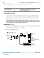
1
Altera I/O Phase-Locked Loop (Altera IOPLL) IP Core
User Guide
2015.05.04
UG-01155
Send Feedback
Subscribe
The Altera IOPLL megafunction IP core allows you to configure the settings of Arria® 10 I/O PLL.
Altera IOPLL IP core supports the following features:
• Supports six different clock feedback modes: direct, external feedback, normal, source synchronous,
zero delay buffer, and LVDS mode.
• Generates up to nine clock output signals for the Arria 10 device.
• Switches between two reference input clocks.
• Supports adjacent PLL (adjpllin) input to connect with an upstream PLL in PLL cascading mode.
• Generates the Memory Initialization File (.mif) and allows PLL dynamic reconfiguration.
• Supports PLL dynamic phase shift.
Related Information
• Introduction to Altera IP Cores
Provides more information about the Altera IP cores and the parameter editor.
• Operation Modes on page 8
• Output Clocks on page 8
• Reference Clock Switchover on page 9
• PLL-to-PLL Cascading on page 9
Device Family Support
The Altera IOPLL IP core only supports the Arria 10 device family.
Altera IOPLL IP Core Parameters
The Altera IOPLL IP core parameter editor appears in the PLL category of the IP Catalog.
Altera IOPLL IP Core Parameters - PLL Tab
Table 1: Altera IOPLL IP Core Parameters - PLL Tab
Parameter
Device Family
Legal Value
Arria 10
Description
Specifies the device family.
© 2015 Altera Corporation. All rights reserved. ALTERA, ARRIA, CYCLONE, ENPIRION, MAX, MEGACORE, NIOS, QUARTUS and STRATIX words and logos are
trademarks of Altera Corporation and registered in the U.S. Patent and Trademark Office and in other countries. All other words and logos identified as
trademarks or service marks are the property of their respective holders as described at www.altera.com/common/legal.html. Altera warrants performance
of its semiconductor products to current specifications in accordance with Altera's standard warranty, but reserves the right to make changes to any
products and services at any time without notice. Altera assumes no responsibility or liability arising out of the application or use of any information,
product, or service described herein except as expressly agreed to in writing by Altera. Altera customers are advised to obtain the latest version of device
specifications before relying on any published information and before placing orders for products or services.
www.altera.com
101 Innovation Drive, San Jose, CA 95134
ISO
9001:2008
Registered
2
UG-01155
2015.05.04
Altera IOPLL IP Core Parameters - PLL Tab
Parameter
Legal Value
Description
Component
—
Specifies the targeted device.
Speed Grade
—
Specifies the speed grade for targeted device.
PLL Mode
Reference Clock
Frequency
Integer-N PLL Specifies the mode used for the Altera IOPLL IP core. The
only legal selection is Integer-N PLL. If you need a fractional
PLL, you must use the Arria 10 FPLL IP core.
—
Specifies the input frequency for the input clock, refclk, in
MHz. The default value is 100.0 MHz. The minimum and
maximum value is dependent on the selected device.
Enable Locked Output
Port
Turn on or
Turn off
Turn on to enable the locked port.
Enable physical output
clock parameters
Turn on or
Turn off
Turn on to enter physical PLL counter parameters instead of
specifying a desired output clock frequency.
Operation Mode
Altera Corporation
direct,
Specifies the operation of the PLL. The default operation is
external
direct mode.
feedback,
• If you select the direct mode, the PLL minimizes the
normal,
length of the feedback path to produce the smallest
source
possible jitter at the PLL output.The internal-clock and
synchronous,
external-clock outputs of the PLL are phase-shifted with
zero delay
respect
to the PLL clock input. In this mode, the PLL does
buffer or lvds
not compensate for any clock networks.
• If you select the normal mode, the PLL compensates for
the delay of the internal clock network used by the clock
output. If the PLL is also used to drive an external clock
output pin, a corresponding phase shift of the signal on
the output pin occurs.
• If you select the source synchronous mode, the clock
delay from pin to I/O input register matches the data
delay from pin to I/O input register.
• If you select the external feedback mode, you must
connect the fbclk input port to an input pin. A boardlevel connection must connect both the input pin and
external clock output port, fboutclk. The fbclk port is
aligned with the input clock.
• If you select the zero delay buffer mode, the PLL must
feed an external clock output pin and compensate for the
delay introduced by that pin. The signal observed on the
pin is synchronized to the input clock. The PLL clock
output connects to the altbidir port and drives
zdbfbclk as an output port. If the PLL also drives the
internal clock network, a corresponding phase shift of
that network occurs.
• If you select the lvds mode, the same data and clock
timing relationship of the pins at the internal SERDES
capture register is maintained. The mode compensates
for the delays in LVDS clock network, and between the
data pin and clock input pin to the SERDES capture
register paths.
Altera I/O Phase-Locked Loop (Altera IOPLL) IP Core User Guide
Send Feedback
UG-01155
2015.05.04
Altera IOPLL IP Core Parameters - PLL Tab
Parameter
Number of Clocks
Specify VCO Frequency
VCO Frequency (1)
Give clock global name
1–9
Description
Specifies the number of output clocks required for each
device in the PLL design. The requested settings for output
frequency, phase shift, and duty cycle are shown based on
the number of clocks selected.
Turn on or
Turn off
Allows you to restrict the VCO frequency to the specified
value. This is useful when creating a PLL for LVDS external
mode, or if a specific dynamic phase shift step size is desired.
—
• When Enable physical output clock parameters is
turned on—displays the VCO frequency based on the
values for Reference Clock Frequency, Multiply Factor
(M-Counter), and Divide Factor (N-Counter).
• When Enable physical output clock parameters is
turned off—allows you to specify the requested value for
the VCO frequency. The default value is 600.0 MHz.
Turn on or
Turn off
Allows you to rename the output clock name.
Clock Name
—
The user clock name for Synopsis Design Constraints (SDC).
Desired Frequency
—
Specifies the output clock frequency of the corresponding
output clock port, outclk[], in MHz. The default value is
100.0 MHz. The minimum and maximum values depend on
the device used. The PLL only reads the numerals in the first
six decimal places.
Actual Frequency
—
Allows you to select the actual output clock frequency from a
list of achievable frequencies. The default value is the closest
achievable frequency to the desired frequency.
Phase Shift units
(1)
Legal Value
3
ps or degrees Specifies the phase shift unit for the corresponding output
clock port, outclk[], in picoseconds (ps) or degrees.
Desired Phase Shift
—
Specifies the requested value for the phase shift. The default
value is 0 ps.
Actual Phase Shift
—
Allows you to select the actual phase shift from a list of
achievable phase shift values. The default value is the closest
achievable phase shift to the desired phase shift.
Desired Duty Cycle
0.0–100.0
Specifies the requested value for the duty cycle. The default
value is 50.0%.
Actual Duty Cycle
—
Allows you to select the actual duty cycle from a list of
achievable duty cycle values. The default value is the closest
achievable duty cycle to the desired duty cycle.
This parameter is only available when Enable physical output clock parameters is turned off.
Altera I/O Phase-Locked Loop (Altera IOPLL) IP Core User Guide
Send Feedback
Altera Corporation
4
UG-01155
2015.05.04
Altera IOPLL IP Core Parameters - Settings Tab
Parameter
Legal Value
Multiply Factor (MCounter) (2)
4–511
Divide Factor (NCounter) (2)
1–511
Divide Factor (CCounter) (2)
1-511
Description
Specifies the multiply factor of M-counter.
The legal range of the M counter is 4–511. However, restric‐
tions on the minimum legal PFD frequency and maximum
legal VCO frequency restrict the effective M counter range to
4–160.
Specifies the divide factor of N-counter.
The legal range of the N counter is 1–511. However, restric‐
tions on the minimum legal PFD frequency restrict the
effective range of the N counter to 1–80.
Specifies the divide factor for the output clock (C-counter).
Altera IOPLL IP Core Parameters - Settings Tab
Table 2: Altera IOPLL IP Core Parameters - Settings Tab
Parameter
PLL Bandwidth Preset
(2)
Legal Value
Description
Low, Medium, Specifies the PLL bandwidth preset setting. The default
or High
selection is Low.
PLL Auto Reset
Turn on or
Turn off
Automatically self-resets the PLL on loss of lock.
Create a second input clk
‘refclk1’
Turn on or
Turn off
Turn on to provide a backup clock attached to your PLL
that can switch with your original reference clock.
Second Reference Clock
Frequency
—
Selects the frequency of the second input clock signal. The
default value is 100.0 MHz. The minimum and maximum
value is dependent on the device used.
Create an ‘active_clk’ signal
to indicate the input clock
in use
Turn on or
Turn off
Turn on to create the activeclk output. The activeclk
output indicates the input clock which is in use by the PLL.
Output signal low indicates refclk and output signal high
indicates refclk1.
Create a ‘clkbad’ signal for
each of the input clocks
Turn on or
Turn off
Turn on to create two clkbad outputs, one for each input
clock. Output signal low indicates the clock is working and
output signal high indicates the clock is not working.
This parameter is only available when Enable physical output clock parameters is turned on.
Altera Corporation
Altera I/O Phase-Locked Loop (Altera IOPLL) IP Core User Guide
Send Feedback
UG-01155
2015.05.04
Altera IOPLL IP Core Parameters - Settings Tab
Parameter
Switchover Mode
Legal Value
Description
Automatic Specifies the switchover mode for design application. The IP
Switchover, supports three switchover modes:
Manual
Switchover, or • If you select the Automatic Switchover mode, the PLL
circuitry monitors the selected reference clock. If one
Automatic
clock stops, the circuit automatically switches to the
Switchover
backup clock in a few clock cycles and updates the status
with Manual
signals,
clkbad and activeclk.
Override
• If you select the Manual Switchover mode, when the
control signal, extswitch, changes from logic low to
logic high, and stays high for at least three clock cycles,
the input clock switches to the other clock. The
extswitch can be generated from FPGA core logic or
input pin.
• If you select Automatic Switchover with Manual
Override mode, when the extswitch signal is high, it
overrides the automatic switch function. As long as
extswitch remains high, further switchover action is
blocked. To select this mode, your two clock sources
must be running and the frequency of the two clocks
cannot differ by more than 20%. If both clocks are not on
the same frequency, but their period difference is within
20%, the clock loss detection block will detect the lost
clock. The PLL most likely drops out of lock after the
PLL clock input switchover and needs time to lock again.
0–7
Turn on to create two clkbad outputs, one for each input
clock. Output signal low indicates the clock is working and
output signal high indicates the clock is not working.
Enable access to PLL
LVDS_CLK/LOADEN
output port
Turn on or
Turn off
Turn on to enable the PLL LVDS_CLK/LOADEN output port.
Enable access to the PLL
DPA output port
Turn on or
Turn off
Turn on to enable the PLL DPA output port.
Enable access to PLL
external clock output port
Turn on or
Turn off
Turn on to enable the PLL external clock output port.
Specifies which outclk to be
used as extclk_out[0]
source
C0 – C8
Specifies the outclk port to be used as extclk_out[0]
source.
Specifies which outclk to be
used as extclk_out[1]
source
C0 – C8
Specifies the outclk port to be used as extclk_out[1]
source.
Switchover Delay
Enables this parameter in case the PLL feeds an LVDS
SERDES block with external PLL. For more information,
refer to the Signal Interface Between Altera IOPLL and
Altera LVDS SERDES IP Cores table in the I/O and High
Speed I/O in Arria 10 Devices chapter.
Altera I/O Phase-Locked Loop (Altera IOPLL) IP Core User Guide
Send Feedback
5
Altera Corporation
6
UG-01155
2015.05.04
Altera IOPLL IP Core Parameters - Cascading Tab
Related Information
Signal Interface Between Altera IOPLL and Altera LVDS SERDES IP Cores
Provides more information about PLL lvds_clk and loaden signals when the PLL is in LVDS mode.
Altera IOPLL IP Core Parameters - Cascading Tab
Table 3: Altera IOPLL IP Core Parameters - Cascading Tab
Parameter
Legal Value
Create a ‘cascade out’ signal
to connect with a
downstream PLL
Turn on or
Turn off
Specifies which outclk to be
used as cascading source
0-8
Create an adjpllin or cclk
signal to connect with an
upstream PLL
Turn on or
Turn off
Description
Turn on to create the cascade_out port, which indicates
that this PLL is a source and connects with a destination
(downstream) PLL.
Specifies the cascading source.
Turn on to create an input port, which indicates that this
PLL is a destination and connects with a source (upstream)
PLL.
Altera IOPLL IP Core Parameters - Dynamic Reconfiguration Tab
Table 4: Altera IOPLL IP Core Parameters - Dynamic Reconfiguration Tab
Parameter
Turn on or
Turn off
Turn on the enable the dynamic reconfiguration of this PLL
(in conjunction with Altera PLL Reconfig IP core).
Enable access to dynamic
phase shift ports
Turn on or
Turn off
Turn on the enable the dynamic phase shift interface with
the PLL.
Generate MIF file (3)
Turn on or
Turn off
Turn on to generate the .mif file for the current PLL profile.
The generated .mif file contains current PLL profile and a
collection of physical parameters—such as M, N, C, K,
bandwidth, and charge pump—that defines that PLL. You
can then load this .mif file into the Altera PLL Reconfig IP
core.
Enable Dynamic Phase
Shift for MIF Streaming (4)
Turn on or
Turn off
Turn on to store dynamic phase shift properties for PLL
reconfiguration.
Number of Dynamic Phase
Shifts (5)
Dynamic Phase Shift
Direction (5)
(4)
(5)
Description
Enable dynamic reconfigu‐
ration of PLL
DPS Counter Selection (5)
(3)
Legal Value
C0–C8, All C, Selects the counter to undergo dynamic phase shift.
or M
1–7
Selects the number of phase shift increments. The size of a
single phase shift increment is equal to 1/8 of the VCO
period. The default value is 1.
Positive or
Negative
Determines the dynamic phase shift direction to store into
the PLL MIF.
This parameter is only available when Enable dynamic reconfiguration of PLL is turned on.
This parameter is only available when Generate MIF file is turned on.
This parameter is only available when Enable Dynamic Phase Shift for MIF Streaming is turned on.
Altera Corporation
Altera I/O Phase-Locked Loop (Altera IOPLL) IP Core User Guide
Send Feedback
UG-01155
2015.05.04
Altera IOPLL IP Core Parameters - Advanced Parameters Tab
7
Altera IOPLL IP Core Parameters - Advanced Parameters Tab
Table 5: Altera IOPLL IP Core Parameters - Advanced Parameters Tab
Parameter
Legal Value
Advanced Parameters
—
Description
Displays a table of physical PLL settings that will be
implemented based on your input.
Functional Description
An I/O PLL is a frequency-control system that generates an output clock by synchronizing itself to an
input clock. The PLL compares the phase difference between the input signal and the output signal of a
voltage-controlled oscillator (VCO) and then performs phase synchronization to maintain a constant
phase angle (lock) on the frequency of the input or reference signal. The synchronization or negative
feedback loop of the system forces the PLL to be phase-locked.
You can configure PLLs as frequency multipliers, dividers, demodulators, tracking generators, or clock
recovery circuits. You can use PLLs to generate stable frequencies, recover signals from a noisy communi‐
cation channel, or distribute clock signals throughout your design.
Building Blocks of a PLL
The main blocks of the I/O PLL are the phase frequency detector (PFD), charge pump, loop filter, VCO,
and counters, such as a feedback counter (M), a pre-scale counter (N), and post-scale counters (C). The PLL
architecture depends on the device you use in your design.
Figure 1: Typical I/O PLL Architecture
To DPA Block
Dedicated Clock Inputs
GCLK/RCLK
Cascade Input
from Adjacent I/O PLL
and Dedicated refclk
4
Lock
Circuit
locked
8
inclk0
Clock
inclk1 Switchover
Block
÷N
PFD
clkswitch
clkbad0
clkbad1
activeclock
CP
LF
VCO
Casade Output
to Adjacent I/O PLL
GCLKs
RCLKs
÷C0
8
÷C1
÷C2
÷C3
PLL Output Multiplexer
For single-ended clock inputs, only the CLKp pin
has a dedicated connection to the PLL. If you use the
CLKn pin, a global or regional clock is used.
÷C8
÷M
Direct Compensation Mode
Zero Delay Buffer, External Feedback Modes
LVDS Compensation Mode
Source Synchronous, Normal Modes
Altera I/O Phase-Locked Loop (Altera IOPLL) IP Core User Guide
Send Feedback
RX/TX Clock
RX/TX Load Enable
FBOUT
External Memory
Interface DLL
This FBOUT port is fed by
the M counter in the PLLs.
FBIN
LVDS Clock Network
GCLK/RCLK Network
Altera Corporation
8
UG-01155
2015.05.04
PLL Lock
The following terms are commonly used to describe the behavior of a PLL:
• PLL lock time—also known as the PLL acquisition time. PLL lock time is the time for the PLL to attain
the target frequency and phase relationship after power-up, after a programmed output frequency
change, or after a PLL reset.
Note: Simulation software does not model a realistic PLL lock time. Simulation shows an unrealisti‐
cally fast lock time. For the actual lock time specification, refer to the device datasheet.
• PLL resolution—the minimum frequency increment value of a PLL VCO. The number of bits in the M
and N counters determine the PLL resolution value.
• PLL sample rate—the FREF sampling frequency required to perform the phase and frequency
correction in the PLL. The PLL sample rate is fREF /N.
PLL Lock
The PLL lock is dependent on the two input signals in the phase frequency detector. The lock signal is an
asynchronous output of the PLLs.
The number of cycles required to gate the lock signal depends on the PLL input clock which clocks the
gated-lock circuitry. Divide the maximum lock time of the PLL by the period of the PLL input clock to
calculate the number of clock cycles required to gate the lock signal.
Operation Modes
The Altera IOPLL IP core supports six different clock feedback modes. Each mode allows clock multipli‐
cation and division, phase shifting, and duty-cycle programming.
The following list describes the operation modes for the Altera IOPLL IP core:
• Direct mode—the PLL minimizes the feedback path length to produce the smallest possible jitter at the
PLL output. In this mode, the PLL does not compensate for any clock networks.
• Normal mode—the PLL feedback path source is a global or regional clock network, minimizing clock
delay from the input clock pin to the core registers through global or regional clock network.
• Source-Synchronous mode—the data and clock signals arrive at the input pins at the same time. In this
mode, the signals have the same phase relationship at the clock and data ports of any Input Output
Enable register.
• External Feedback mode—the PLL compensates for the fbclk feedback input to the PLL, thus
minimizing the delay between the input clock pin and the feedback clock pin.
• Zero-Delay Buffer mode—the PLL feedback path is confined to the dedicated PLL external output pin.
The clock port driven off-chip is phase aligned with the clock input for a minimal delay between the
clock input and the external clock output.
• LVDS mode— maintains the same data and clock timing relationship of the pins at the internal
SERDES capture register. This mode compensates for the LVDS clock network delay, plus any delay
difference between the data pin and clock input pin to the SERDES capture register paths. The
compensation mimic path mimics the clock and data delay of the receiver side.
Output Clocks
The Altera IOPLL IP core can generate up to nine clock output signals. The generated clock output signals
clock the core or the external blocks outside the core.
You can use the reset signal to reset the output clock value to 0 and disable the PLL output clocks.
Altera Corporation
Altera I/O Phase-Locked Loop (Altera IOPLL) IP Core User Guide
Send Feedback
UG-01155
2015.05.04
Reference Clock Switchover
9
Each output clock has a set of requested settings where you can specify the desired values for output
frequency, phase shift, and duty cycle. The desired settings are the settings that you want to implement in
your design.
The actual values for the frequency, phase shift, and duty cycle are the closest settings (best approximate
of the desired settings) that can be implemented in the PLL circuit.
Reference Clock Switchover
The reference clock switchover feature allows the PLL to switch between two reference input clocks. Use
this feature for clock redundancy, or for a dual clock domain application such as in a system. The system
can turn on a redundant clock if the primary clock stops running.
Using the reference clock switchover feature, you can specify the frequency for the second input clock,
and select the mode and delay for the switchover.
The clock loss detection and reference clock switchover block has the following functions:
• Monitors the reference clock status. If the reference clock fails, the clock automatically switches to a
backup clock input source. The clock updates the status of the clkbad and activeclk signals to alert
the event.
• Switches the reference clock back and forth between two different frequencies. Use the extswitch
signal to manually control the switch action. After a switchover occurs, the PLL may lose lock
temporarily and go through the reckoning process.
PLL-to-PLL Cascading
If you cascade PLLs in your design, the source (upstream) PLL must have a low-bandwidth setting, while
the destination (downstream) PLL must have a high-bandwidth setting. During cascading, the output of
source PLL serves as the reference clock (input) of the destination PLL. The bandwidth settings of
cascaded PLLs must be different. If the bandwidth settings of the cascaded PLLs are the same, the
cascaded PLLs may amplify phase noise at certain frequencies.
The adjpllin input clock source is used for inter-cascading between fracturable fractional PLLs.
Ports
Table 6: Altera IOPLL Ports
Parameter
Type
Condition
refclk
Input
Required
The reference clock source that drives the I/O
PLL.
rst
Input
Required
The asynchronous reset port for the output
clocks. Drive this port high to reset all output
clocks to the value of 0.
Altera I/O Phase-Locked Loop (Altera IOPLL) IP Core User Guide
Send Feedback
Description
Altera Corporation
10
UG-01155
2015.05.04
Ports
Parameter
fbclk
Type
Condition
Input
Optional
Description
The external feedback input port for the I/O
PLL.
The Altera IOPLL IP core creates this port when
the I/O PLL is operating in external feedback
mode or zero-delay buffer mode. To complete
the feedback loop, a board-level connection must
connect the fbclk port and the external clock
output port of the I/O PLL.
fboutclk
Output
Optional
The port that feeds the fbclk port through the
mimic circuitry.
The fboutclk port is available only if the I/O
PLL is in external feedback mode.
zdbfbclk
Bidirectional
Optional
The bidirectional port that connects to the
mimic circuitry. This port must connect to a
bidirectional pin that is placed on the positive
feedback dedicated output pin of the I/O PLL.
The zdbfbclk port is available only if the I/O
PLL is in zero-delay buffer mode.
Output
Optional
The Altera IOPLL IP core drives this port high
when the PLL acquires lock. The port remains
high as long as the IOPLL is locked. The I/O PLL
asserts the locked port when the phases and
frequencies of the reference clock and feedback
clock are the same or within the lock circuit
tolerance. When the difference between the two
clock signals exceeds the lock circuit tolerance,
the I/O PLL loses lock.
refclk1
Input
Optional
Second reference clock source that drives the I/O
PLL for clock switchover feature.
extswitch
Input
Optional
Assert the extswitch signal high (1’b1) for at
least 3 clock cycles to manually switch the clock.
activeclk
Output
Optional
Output signal to indicate which reference clock
source is in used by I/O PLL.
clkbad
Output
Optional
Output signal that indicates the status of
reference clock source is good or bad.
cascade_out
Output
Optional
Output signal that feeds into downstream I/O
PLL.
adjpllin
Input
Optional
Input signal that feeds from upstream I/O PLL.
outclk_[]
Output
Optional
Output clock from I/O PLL.
locked
Altera Corporation
Altera I/O Phase-Locked Loop (Altera IOPLL) IP Core User Guide
Send Feedback
UG-01155
2015.05.04
Document Revision History
11
Document Revision History
Date
Version
Changes
May 2015
2015.05.04
Updated the description for Enable access to PLL LVDS_CLK/LOADEN
output port parameter in Altera IOPLL IP Core Parameters - Settings
Tab table. Added a link to the Signal Interface Between Altera IOPLL
and Altera LVDS SERDES IP Cores table in the I/O and High Speed I/O
in Arria 10 Devices chapter.
August 2014
2014.08.18
Initial release.
Altera I/O Phase-Locked Loop (Altera IOPLL) IP Core User Guide
Send Feedback
Altera Corporation