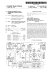
1
Cyclone V Device Handbook
Volume 1: Device Interfaces and Integration
Subscribe
Send Feedback
CV-5V2
2013.11.12
101 Innovation Drive
San Jose, CA 95134
www.altera.com
TOC-2
Cyclone V Device Handbook Volume 1: Device Interfaces and Integration
Contents
Logic Array Blocks and Adaptive Logic Modules in Cyclone V Devices...........1-1
LAB ...............................................................................................................................................................1-1
MLAB ................................................................................................................................................1-2
Local and Direct Link Interconnects ............................................................................................1-3
LAB Control Signals........................................................................................................................1-4
ALM Resources ...............................................................................................................................1-5
ALM Output ....................................................................................................................................1-6
ALM Operating Modes ..............................................................................................................................1-7
Normal Mode ..................................................................................................................................1-8
Extended LUT Mode ......................................................................................................................1-8
Arithmetic Mode .............................................................................................................................1-8
Shared Arithmetic Mode ................................................................................................................1-9
Document Revision History.....................................................................................................................1-10
Embedded Memory Blocks in Cyclone V Devices..............................................2-1
Types of Embedded Memory.....................................................................................................................2-1
Embedded Memory Capacity in Cyclone V Devices..................................................................2-1
Embedded Memory Design Guidelines for Cyclone V Devices............................................................2-2
Guideline: Consider the Memory Block Selection......................................................................2-2
Guideline: Implement External Conflict Resolution..................................................................2-3
Guideline: Customize Read-During-Write Behavior.................................................................2-3
Guideline: Consider Power-Up State and Memory Initialization............................................2-6
Guideline: Control Clocking to Reduce Power Consumption..................................................2-7
Embedded Memory Features.....................................................................................................................2-7
Embedded Memory Configurations.............................................................................................2-8
Mixed-Width Port Configurations................................................................................................2-9
Embedded Memory Modes......................................................................................................................2-10
Embedded Memory Clocking Modes.....................................................................................................2-11
Clocking Modes for Each Memory Mode..................................................................................2-11
Asynchronous Clears in Clocking Modes..................................................................................2-12
Output Read Data in Simultaneous Read/Write.......................................................................2-12
Independent Clock Enables in Clocking Modes.......................................................................2-13
Parity Bit in Memory Blocks....................................................................................................................2-13
Altera Corporation
Cyclone V Device Handbook Volume 1: Device Interfaces and Integration
TOC-3
Byte Enable in Embedded Memory Blocks............................................................................................2-13
Byte Enable Controls in Memory Blocks....................................................................................2-13
Data Byte Output...........................................................................................................................2-14
RAM Blocks Operations...............................................................................................................2-14
Memory Blocks Packed Mode Support..................................................................................................2-15
Memory Blocks Address Clock Enable Support....................................................................................2-15
Document Revision History.....................................................................................................................2-16
Variable Precision DSP Blocks in Cyclone V Devices........................................3-1
Features.........................................................................................................................................................3-1
Supported Operational Modes in Cyclone V Devices............................................................................3-2
Resources.......................................................................................................................................................3-3
Design Considerations................................................................................................................................3-4
Operational Modes..........................................................................................................................3-4
Internal Coefficient and Pre-Adder...............................................................................................3-4
Accumulator.....................................................................................................................................3-4
Chainout Adder................................................................................................................................3-4
Block Architecture.......................................................................................................................................3-5
Input Register Bank.........................................................................................................................3-6
Pre-Adder..........................................................................................................................................3-8
Internal Coefficient..........................................................................................................................3-8
Multipliers.........................................................................................................................................3-8
Adder.................................................................................................................................................3-9
Accumulator and Chainout Adder................................................................................................3-9
Systolic Registers............................................................................................................................3-10
Double Accumulation Register....................................................................................................3-10
Output Register Bank....................................................................................................................3-10
Operational Mode Descriptions..............................................................................................................3-11
Independent Multiplier Mode.....................................................................................................3-11
Independent Complex Multiplier Mode....................................................................................3-13
Multiplier Adder Sum Mode........................................................................................................3-15
18 x 18 Multiplication Summed with 36-Bit Input Mode........................................................3-15
Systolic FIR Mode..........................................................................................................................3-16
Document Revision History.....................................................................................................................3-18
Clock Networks and PLLs in Cyclone V Devices................................................4-1
Clock Networks............................................................................................................................................4-1
Clock Resources in Cyclone V Devices.........................................................................................4-1
Altera Corporation
TOC-4
Cyclone V Device Handbook Volume 1: Device Interfaces and Integration
Types of Clock Networks................................................................................................................4-3
Clock Sources Per Quadrant..........................................................................................................4-5
Types of Clock Regions...................................................................................................................4-6
Clock Network Sources...................................................................................................................4-7
Clock Output Connections.............................................................................................................4-9
Clock Control Block........................................................................................................................4-9
Clock Power Down........................................................................................................................4-12
Clock Enable Signals......................................................................................................................4-12
Cyclone V PLLs..........................................................................................................................................4-14
PLL Physical Counters in Cyclone V Devices............................................................................4-15
PLL Locations in Cyclone V Devices..........................................................................................4-15
Fractional PLL Architecture.........................................................................................................4-18
PLL External Clock I/O Pins........................................................................................................4-19
PLL Control Signals.......................................................................................................................4-20
Clock Feedback Modes..................................................................................................................4-21
Clock Multiplication and Division..............................................................................................4-27
Programmable Duty Cycle...........................................................................................................4-28
Clock Switchover...........................................................................................................................4-28
PLL Reconfiguration and Dynamic Phase Shift........................................................................4-33
Document Revision History.....................................................................................................................4-33
I/O Features in Cyclone V Devices......................................................................5-1
I/O Resources Per Package for Cyclone V Devices.................................................................................5-1
I/O Vertical Migration for Cyclone V Devices........................................................................................5-4
Verifying Pin Migration Compatibility........................................................................................5-5
I/O Standards Support in Cyclone V Devices..........................................................................................5-5
I/O Standards Support for FPGA I/O in Cyclone V Devices....................................................5-5
I/O Standards Support for HPS I/O in Cyclone V Devices........................................................5-7
I/O Standards Voltage Levels in Cyclone V Devices...................................................................5-8
MultiVolt I/O Interface in Cyclone V Devices..........................................................................5-10
I/O Design Guidelines for Cyclone V Devices.......................................................................................5-11
Mixing Voltage-Referenced and Non-Voltage-Referenced I/O Standards...........................5-11
PLLs and Clocking.........................................................................................................................5-12
LVDS Interface with External PLL Mode...................................................................................5-15
Guideline: Use the Same VCCPD for All I/O Banks in a Group...............................................5-17
Guideline: Ensure Compatible VCCIO and VCCPD Voltage in the Same Bank......................5-18
Guideline: VREF Pin Restrictions...............................................................................................5-18
Guideline: Observe Device Absolute Maximum Rating for 3.3 V Interfacing......................5-18
Altera Corporation
Cyclone V Device Handbook Volume 1: Device Interfaces and Integration
TOC-5
Guideline: Adhere to the LVDS I/O Restrictions and Differential Pad Placement
Rules...........................................................................................................................................5-19
I/O Banks Locations in Cyclone V Devices............................................................................................5-19
I/O Banks Groups in Cyclone V Devices...............................................................................................5-21
Modular I/O Banks for Cyclone V E Devices............................................................................5-21
Modular I/O Banks for Cyclone V GX Devices.........................................................................5-22
Modular I/O Banks for Cyclone V GT Devices.........................................................................5-23
Modular I/O Banks for Cyclone V SE Devices..........................................................................5-24
Modular I/O Banks for Cyclone V SX Devices..........................................................................5-25
Modular I/O Banks for Cyclone V ST Devices..........................................................................5-26
I/O Element Structure in Cyclone V Devices........................................................................................5-26
I/O Buffer and Registers in Cyclone V Devices.........................................................................5-27
Programmable IOE Features in Cyclone V Devices.............................................................................5-28
Programmable Current Strength.................................................................................................5-29
Programmable Output Slew-Rate Control.................................................................................5-30
Programmable IOE Delay.............................................................................................................5-30
Programmable Output Buffer Delay...........................................................................................5-30
Programmable Pre-Emphasis......................................................................................................5-31
Programmable Differential Output Voltage..............................................................................5-31
I/O Pins Features for Cyclone V Devices...............................................................................................5-32
Open-Drain Output.......................................................................................................................5-32
Bus-Hold Circuitry........................................................................................................................5-33
Pull-up Resistor..............................................................................................................................5-33
On-Chip I/O Termination in Cyclone V Devices.................................................................................5-33
RS OCT without Calibration in Cyclone V Devices..................................................................5-34
RS OCT with Calibration in Cyclone V Devices........................................................................5-35
RT OCT with Calibration in Cyclone V Devices.......................................................................5-37
Dynamic OCT in Cyclone V Devices..........................................................................................5-39
LVDS Input RD OCT in Cyclone V Devices..............................................................................5-40
OCT Calibration Block in Cyclone V Devices...........................................................................5-41
External I/O Termination for Cyclone V Devices.................................................................................5-43
Single-ended I/O Termination.....................................................................................................5-44
Differential I/O Termination.......................................................................................................5-46
Dedicated High-Speed Circuitries...........................................................................................................5-51
High-Speed Differential I/O Locations.......................................................................................5-51
LVDS SERDES Circuitry..............................................................................................................5-53
True LVDS Buffers in Cyclone V Devices..................................................................................5-54
Emulated LVDS Buffers in Cyclone V Devices.........................................................................5-62
Differential Transmitter in Cyclone V Devices.....................................................................................5-62
Altera Corporation
TOC-6
Cyclone V Device Handbook Volume 1: Device Interfaces and Integration
Transmitter Blocks.........................................................................................................................5-62
Serializer Bypass for DDR and SDR Operations.......................................................................5-63
Differential Receiver in Cyclone V Devices...........................................................................................5-64
Receiver Blocks in Cyclone V Devices........................................................................................5-64
Receiver Mode in Cyclone V Devices.........................................................................................5-66
Receiver Clocking for Cyclone V Devices..................................................................................5-67
Differential I/O Termination for Cyclone V Devices...............................................................5-67
Source-Synchronous Timing Budget......................................................................................................5-68
Differential Data Orientation.......................................................................................................5-68
Differential I/O Bit Position.........................................................................................................5-69
Transmitter Channel-to-Channel Skew.....................................................................................5-70
Receiver Skew Margin for LVDS Mode......................................................................................5-70
Document Revision History.....................................................................................................................5-72
External Memory Interfaces in Cyclone V Devices............................................6-1
External Memory Performance..................................................................................................................6-2
HPS External Memory Performance.........................................................................................................6-2
Memory Interface Pin Support in Cyclone V Devices............................................................................6-2
Guideline: Using DQ/DQS Pins....................................................................................................6-3
DQ/DQS Bus Mode Pins for Cyclone V Devices........................................................................6-3
DQ/DQS Groups in Cyclone V E..................................................................................................6-4
DQ/DQS Groups in Cyclone V GX...............................................................................................6-6
DQ/DQS Groups in Cyclone V GT...............................................................................................6-9
DQ/DQS Groups in Cyclone V SX..............................................................................................6-11
DQ/DQS Groups in Cyclone V ST..............................................................................................6-11
External Memory Interface Features in Cyclone V Devices................................................................6-11
UniPHY IP......................................................................................................................................6-12
External Memory Interface Datapath.........................................................................................6-12
DQS Phase-Shift Circuitry............................................................................................................6-13
PHY Clock (PHYCLK) Networks...............................................................................................6-20
DQS Logic Block............................................................................................................................6-22
Dynamic OCT Control.................................................................................................................6-24
IOE Registers..................................................................................................................................6-25
Delay Chains...................................................................................................................................6-27
I/O and DQS Configuration Blocks............................................................................................6-28
Hard Memory Controller.........................................................................................................................6-29
Features of the Hard Memory Controller..................................................................................6-29
Multi-Port Front End....................................................................................................................6-31
Altera Corporation
Cyclone V Device Handbook Volume 1: Device Interfaces and Integration
TOC-7
Bonding Support............................................................................................................................6-32
Hard Memory Controller Width for Cyclone V E....................................................................6-34
Hard Memory Controller Width for Cyclone V GX................................................................6-35
Hard Memory Controller Width for Cyclone V GT................................................................6-36
Hard Memory Controller Width for Cyclone V SX.................................................................6-36
Hard Memory Controller Width for Cyclone V ST..................................................................6-36
Document Revision History.....................................................................................................................6-37
Configuration, Design Security, and Remote System Upgrades in Cyclone V
Devices.............................................................................................................7-1
Enhanced Configuration and Configuration via Protocol.....................................................................7-1
MSEL Pin Settings........................................................................................................................................7-2
Configuration Sequence..............................................................................................................................7-3
Power Up...........................................................................................................................................7-4
Reset...................................................................................................................................................7-5
Configuration...................................................................................................................................7-5
Configuration Error Handling.......................................................................................................7-5
Initialization......................................................................................................................................7-6
User Mode.........................................................................................................................................7-6
Device Configuration Pins..........................................................................................................................7-6
Configuration Pin Options in the Quartus II Software..............................................................7-8
Fast Passive Parallel Configuration...........................................................................................................7-9
Fast Passive Parallel Single-Device Configuration......................................................................7-9
Fast Passive Parallel Multi-Device Configuration.......................................................................7-9
Active Serial Configuration......................................................................................................................7-11
DATA Clock (DCLK)....................................................................................................................7-11
Active Serial Single-Device Configuration.................................................................................7-12
Active Serial Multi-Device Configuration..................................................................................7-13
Estimating the Active Serial Configuration Time.....................................................................7-14
Using EPCS and EPCQ Devices..............................................................................................................7-15
Controlling EPCS and EPCQ Devices........................................................................................7-15
Trace Length and Loading............................................................................................................7-15
Programming EPCS and EPCQ Devices....................................................................................7-15
Passive Serial Configuration.....................................................................................................................7-19
Passive Serial Single-Device Configuration Using an External Host.....................................7-20
Passive Serial Single-Device Configuration Using an Altera Download Cable....................7-20
Passive Serial Multi-Device Configuration................................................................................7-21
JTAG Configuration..................................................................................................................................7-23
Altera Corporation
TOC-8
Cyclone V Device Handbook Volume 1: Device Interfaces and Integration
JTAG Single-Device Configuration.............................................................................................7-24
JTAG Multi-Device Configuration.............................................................................................7-26
CONFIG_IO JTAG Instruction...................................................................................................7-26
Configuration Data Compression...........................................................................................................7-27
Enabling Compression Before Design Compilation.................................................................7-27
Enabling Compression After Design Compilation...................................................................7-27
Using Compression in Multi-Device Configuration................................................................7-27
Remote System Upgrades.........................................................................................................................7-28
Configuration Images....................................................................................................................7-29
Configuration Sequence in the Remote Update Mode.............................................................7-29
Remote System Upgrade Circuitry..............................................................................................7-30
Enabling Remote System Upgrade Circuitry.............................................................................7-30
Remote System Upgrade Registers..............................................................................................7-31
Remote System Upgrade State Machine.....................................................................................7-32
User Watchdog Timer...................................................................................................................7-33
Design Security...........................................................................................................................................7-33
ALTCHIP_ID Megafunction.......................................................................................................7-34
JTAG Secure Mode........................................................................................................................7-34
Security Key Types.........................................................................................................................7-35
Security Modes...............................................................................................................................7-35
Design Security Implementation Steps.......................................................................................7-36
Document Revision History.....................................................................................................................7-37
SEU Mitigation for Cyclone V Devices...............................................................8-1
Error Detection Features.............................................................................................................................8-1
Configuration Error Detection..................................................................................................................8-1
User Mode Error Detection........................................................................................................................8-1
Specifications................................................................................................................................................8-2
Minimum EMR Update Interval...................................................................................................8-2
Error Detection Frequency.............................................................................................................8-3
CRC Calculation Time....................................................................................................................8-3
Using Error Detection Features in User Mode........................................................................................8-4
Enabling Error Detection................................................................................................................8-4
CRC_ERROR Pin.............................................................................................................................8-5
Error Detection Registers................................................................................................................8-5
Error Detection Process..................................................................................................................8-7
Testing the Error Detection Block.................................................................................................8-8
Document Revision History.......................................................................................................................8-9
Altera Corporation
Cyclone V Device Handbook Volume 1: Device Interfaces and Integration
TOC-9
JTAG Boundary-Scan Testing in Cyclone V Devices.........................................9-1
BST Operation Control ..............................................................................................................................9-1
IDCODE ...........................................................................................................................................9-1
Supported JTAG Instruction .........................................................................................................9-3
JTAG Secure Mode .........................................................................................................................9-6
JTAG Private Instruction ...............................................................................................................9-6
I/O Voltage for JTAG Operation ..............................................................................................................9-6
Performing BST ...........................................................................................................................................9-7
Enabling and Disabling IEEE Std. 1149.1 BST Circuitry ......................................................................9-8
Guidelines for IEEE Std. 1149.1 Boundary-Scan Testing.......................................................................9-8
IEEE Std. 1149.1 Boundary-Scan Register ...............................................................................................9-9
Boundary-Scan Cells of a Cyclone V Device I/O Pin.................................................................9-9
Document Revision History.....................................................................................................................9-11
Power Management in Cyclone V Devices.......................................................10-1
Power Consumption..................................................................................................................................10-1
Dynamic Power Equation.............................................................................................................10-1
Hot-Socketing Feature..............................................................................................................................10-2
Hot-Socketing Implementation...............................................................................................................10-2
Power-Up Sequence..................................................................................................................................10-3
Power-On Reset Circuitry........................................................................................................................10-5
Power Supplies Monitored and Not Monitored by the POR Circuitry.................................10-6
Document Revision History.....................................................................................................................10-7
Altera Corporation
1
Logic Array Blocks and Adaptive Logic Modules
in Cyclone V Devices
2013.05.06
CV-52001
Subscribe
Send Feedback
This chapter describes the features of the logic array block (LAB) in the Cyclone® V core fabric.
The LAB is composed of basic building blocks known as adaptive logic modules (ALMs) that you can
configure to implement logic functions, arithmetic functions, and register functions.
You can use a quarter of the available LABs in the Cyclone V devices as a memory LAB (MLAB).
The Quartus® II software and other supported third-party synthesis tools, in conjunction with parameterized
functions such as the library of parameterized modules (LPM), automatically choose the appropriate mode
for common functions such as counters, adders, subtractors, and arithmetic functions.
This chapter contains the following sections:
• LAB
• ALM Operating Modes
Related Information
Cyclone V Device Handbook: Known Issues
Lists the planned updates to the Cyclone V Device Handbook chapters.
LAB
The LABs are configurable logic blocks that consist of a group of logic resources. Each LAB contains dedicated
logic for driving control signals to its ALMs.
MLAB is a superset of the LAB and includes all the LAB features.
© 2013 Altera Corporation. All rights reserved. ALTERA, ARRIA, CYCLONE, HARDCOPY, MAX, MEGACORE, NIOS, QUARTUS and STRATIX words
and logos are trademarks of Altera Corporation and registered in the U.S. Patent and Trademark Office and in other countries. All other
words and logos identified as trademarks or service marks are the property of their respective holders as described at
www.altera.com/common/legal.html. Altera warrants performance of its semiconductor products to current specifications in accordance with
Altera's standard warranty, but reserves the right to make changes to any products and services at any time without notice. Altera assumes
no responsibility or liability arising out of the application or use of any information, product, or service described herein except as expressly
agreed to in writing by Altera. Altera customers are advised to obtain the latest version of device specifications before relying on any published
information and before placing orders for products or services.
www.altera.com
101 Innovation Drive, San Jose, CA 95134
ISO
9001:2008
Registered
1-2
CV-52001
2013.05.06
MLAB
Figure 1-1: LAB Structure and Interconnects Overview in Cyclone V Devices
This figure shows an overview of the Cyclone V LAB and MLAB structure with the LAB interconnects.
C2/C4
C12
Row Interconnects of
Variable Speed and Length
R14
R3/R6
ALMs
Connects to adjacent
LABs, memory blocks,
digital signal processing
(DSP) blocks, or I/O
element (IOE) outputs.
Direct-Link
Interconnect from
Adjacent Block
Direct-Link
Interconnect from
Adjacent Block
Direct-Link
Interconnect to
Adjacent Block
Direct-Link
Interconnect to
Adjacent Block
Local Interconnect
LAB
MLAB
Fast Local Interconnect Is Driven
from Either Sides by Column Interconnect
and LABs, and from Above by Row Interconnect
Column Interconnects of
Variable Speed and Length
MLAB
Each MLAB supports a maximum of 640 bits of simple dual-port SRAM.
You can configure each ALM in an MLAB as a 32 x 2 memory block, resulting in a configuration of 32 x 20
simple dual-port SRAM block.
Altera Corporation
Logic Array Blocks and Adaptive Logic Modules in Cyclone V Devices
Send Feedback
CV-52001
2013.05.06
Local and Direct Link Interconnects
1-3
Figure 1-2: LAB and MLAB Structure for Cyclone V Devices
You can use an MLAB
ALM as a regular LAB
ALM or configure it as a
dual-port SRAM.
LUT-Based-32 x 2
Simple Dual-Port SRAM
ALM
LUT-Based-32 x 2
Simple Dual-Port SRAM
ALM
LUT-Based-32 x 2
Simple Dual-Port SRAM
ALM
LUT-Based-32 x 2
Simple Dual-Port SRAM
ALM
LUT-Based-32 x 2
Simple Dual-Port SRAM
ALM
LAB Control Block
You can use an MLAB
ALM as a regular LAB
ALM or configure it as a
dual-port SRAM.
LAB Control Block
LUT-Based-32 x 2
Simple Dual-Port SRAM
ALM
LUT-Based-32 x 2
Simple Dual-Port SRAM
ALM
LUT-Based-32 x 2
Simple Dual-Port SRAM
ALM
LUT-Based-32 x 2
Simple Dual-Port SRAM
ALM
LUT-Based-32 x 2
Simple Dual-Port SRAM
ALM
MLAB
LAB
Local and Direct Link Interconnects
Each LAB can drive 30 ALMs through fast-local and direct-link interconnects. Ten ALMs are in any given
LAB and ten ALMs are in each of the adjacent LABs.
The local interconnect can drive ALMs in the same LAB using column and row interconnects and ALM
outputs in the same LAB.
Neighboring LABs, MLABs, M10K blocks, or digital signal processing (DSP) blocks from the left or right
can also drive the LAB’s local interconnect using the direct link connection.
The direct link connection feature minimizes the use of row and column interconnects, providing higher
performance and flexibility.
Logic Array Blocks and Adaptive Logic Modules in Cyclone V Devices
Send Feedback
Altera Corporation
1-4
CV-52001
2013.05.06
LAB Control Signals
Figure 1-3: LAB Fast Local and Direct Link Interconnects for Cyclone V Devices
Direct Link Interconnect from
Left LAB, Memory Block,
DSP Block, or IOE Output
Direct Link Interconnect from
Right LAB, Memory Block,
DSP Block, or IOE Output
ALMs
ALMs
Direct Link
Interconnect
to Left
Direct Link
Interconnect
to Right
Fast Local
Interconnect
MLAB
LAB
LAB Control Signals
Each LAB contains dedicated logic for driving the control signals to its ALMs, and has two unique clock
sources and three clock enable signals.
The LAB control block generates up to three clocks using the two clock sources and three clock enable
signals. Each clock and the clock enable signals are linked.
De-asserting the clock enable signal turns off the corresponding LAB-wide clock.
Altera Corporation
Logic Array Blocks and Adaptive Logic Modules in Cyclone V Devices
Send Feedback
CV-52001
2013.05.06
1-5
ALM Resources
Figure 1-4: LAB-Wide Control Signals for Cyclone V Devices
This figure shows the clock sources and clock enable signals in a LAB.
There are two unique
clock signals per LAB.
6
Dedicated Row
LAB Clocks
6
6
Local Interconnect
Local Interconnect
Local Interconnect
Local Interconnect
labclk0
labclk1
labclkena0
or asyncload
or labpreset
labclr1
syncload
labclk2
labclkena1
labclkena2
labclr0
synclr
ALM Resources
One ALM contains four programmable registers. Each register has the following ports:
•
•
•
•
Data
Clock
Synchronous and asynchronous clear
Synchronous load
Global signals, general-purpose I/O (GPIO) pins, or any internal logic can drive the clock and clear control
signals of an ALM register.
GPIO pins or internal logic drives the clock enable signal.
For combinational functions, the registers are bypassed and the output of the look-up table (LUT) drives
directly to the outputs of an ALM.
Note: The Quartus II software automatically configures the ALMs for optimized performance.
Logic Array Blocks and Adaptive Logic Modules in Cyclone V Devices
Send Feedback
Altera Corporation
1-6
CV-52001
2013.05.06
ALM Output
Figure 1-5: ALM High-Level Block Diagram for Cyclone V Devices
shared_arith_in
carry_in
Combinational/
Memory ALUT0
dataf0
datae0
6-Input
LUT
adder0
labclk
To General or
Local Routing
D
Q
dataa
To General or
Local Routing
reg0
datab
To General or
Local Routing
D
Q
reg1
Combinational/
Memory ALUT1
datac
adder1
datad
datae1
D
6-Input
LUT
Q
To General or
Local Routing
To General or
Local Routing
reg2
dataf1
D
shared_arith_out
To General or
Local Routing
carry_out
Q
To General or
Local Routing
reg3
To General or
Local Routing
ALM Output
The general routing outputs in each ALM drive the local, row, and column routing resources. Two ALM
outputs can drive column, row, or direct link routing connections, and one of these ALM outputs can also
drive local interconnect resources.
The LUT, adder, or register output can drive the ALM outputs. The LUT or adder can drive one output
while the register drives another output.
Register packing improves device utilization by allowing unrelated register and combinational logic to be
packed into a single ALM. Another mechanism to improve fitting is to allow the register output to feed back
into the look-up table (LUT) of the same ALM so that the register is packed with its own fan-out LUT. The
ALM can also drive out registered and unregistered versions of the LUT or adder output.
Altera Corporation
Logic Array Blocks and Adaptive Logic Modules in Cyclone V Devices
Send Feedback
CV-52001
2013.05.06
ALM Operating Modes
1-7
Figure 1-6: ALM Connection Details for Cyclone V Devices
shared_arith_in carry_in
syncload
aclr[1:0]
clk[2:0] sclr
dataf0
datae0
dataa
datab
datac0
GND
4-Input
LUT
+
D
3-Input
LUT
3-Input
LUT
D
CLR
Q
CLR
Q
Row, Column
Direct Link Routing
Row, Column
Direct Link Routing
Local
Interconnect
datac1
4-Input
LUT
D
+
CLR
Q
Row, Column
Direct Link Routing
3-Input
LUT
3-Input
LUT
VCC
D
CLR
Q
Row, Column
Direct Link Routing
Local
Interconnect
datae1
dataf1
shared_arith_out carry_out
ALM Operating Modes
The Cyclone V ALM operates in any of the following modes:
•
•
•
•
Normal mode
Extended LUT mode
Arithmetic mode
Shared arithmetic mode
Logic Array Blocks and Adaptive Logic Modules in Cyclone V Devices
Send Feedback
Altera Corporation
1-8
CV-52001
2013.05.06
Normal Mode
Normal Mode
Normal mode allows two functions to be implemented in one Cyclone V ALM, or a single function of up
to six inputs.
Up to eight data inputs from the LAB local interconnect are inputs to the combinational logic.
The ALM can support certain combinations of completely independent functions and various combinations
of functions that have common inputs.
Extended LUT Mode
In this mode, if the 7-input function is unregistered, the unused eighth input is available for register packing.
Functions that fit into the template, as shown in the following figure, often appear in designs as “if-else”
statements in Verilog HDL or VHDL code.
Figure 1-7: Template for Supported 7-Input Functions in Extended LUT Mode for Cyclone V Devices
datae0
datac
dataa
datab
datad
dataf0
5-Input
LUT
To General or
Local Routing
combout0
D
datae1
5-Input
LUT
Q
To General or
Local Routing
reg0
dataf1
This input is available
for register packing.
Arithmetic Mode
The ALM in arithmetic mode uses two sets of two 4-input LUTs along with two dedicated full adders.
The dedicated adders allow the LUTs to perform pre-adder logic; therefore, each adder can add the output
of two 4-input functions.
The ALM supports simultaneous use of the adder’s carry output along with combinational logic outputs.
The adder output is ignored in this operation.
Using the adder with the combinational logic output provides resource savings of up to 50% for functions
that can use this mode.
Altera Corporation
Logic Array Blocks and Adaptive Logic Modules in Cyclone V Devices
Send Feedback
CV-52001
2013.05.06
Shared Arithmetic Mode
1-9
Figure 1-8: ALM in Arithmetic Mode for Cyclone V Devices
carry_in
datae0
adder0
4-Input
LUT
dataf0
datac
datab
dataa
reg0
4-Input
LUT
To General or
Local Routing
reg1
datad
datae1
dataf1
adder1
4-Input
LUT
4-Input
LUT
reg2
To General or
Local Routing
carry_out
reg3
Carry Chain
The carry chain provides a fast carry function between the dedicated adders in arithmetic or shared arithmetic
mode.
The two-bit carry select feature in Cyclone V devices halves the propagation delay of carry chains within
the ALM. Carry chains can begin in either the first ALM or the fifth ALM in a LAB. The final carry-out
signal is routed to an ALM, where it is fed to local, row, or column interconnects.
To avoid routing congestion in one small area of the device when a high fan-in arithmetic function is
implemented, the LAB can support carry chains that only use either the top half or bottom half of the LAB
before connecting to the next LAB. This leaves the other half of the ALMs in the LAB available for
implementing narrower fan-in functions in normal mode. Carry chains that use the top five ALMs in the
first LAB carry into the top half of the ALMs in the next LAB in the column. Carry chains that use the bottom
five ALMs in the first LAB carry into the bottom half of the ALMs in the next LAB within the column. You
can bypass the top-half of the LAB columns and bottom-half of the MLAB columns.
The Quartus II Compiler creates carry chains longer than 20 ALMs (10 ALMs in arithmetic or shared
arithmetic mode) by linking LABs together automatically. For enhanced fitting, a long carry chain runs
vertically, allowing fast horizontal connections to the TriMatrix memory and DSP blocks. A carry chain can
continue as far as a full column.
Shared Arithmetic Mode
The ALM in shared arithmetic mode can implement a 3-input add in the ALM.
This mode configures the ALM with four 4-input LUTs. Each LUT either computes the sum of three inputs
or the carry of three inputs. The output of the carry computation is fed to the next adder using a dedicated
connection called the shared arithmetic chain.
Logic Array Blocks and Adaptive Logic Modules in Cyclone V Devices
Send Feedback
Altera Corporation
1-10
CV-52001
2013.05.06
Document Revision History
Figure 1-9: ALM in Shared Arithmetic Mode for Cyclone V Devices
shared_arith_in
carry_in
labclk
4-Input
LUT
datae0
datac
datab
dataa
reg0
4-Input
LUT
reg1
4-Input
LUT
datad
datae1
To General or
Local Routing
reg2
4-Input
LUT
shared_arith_out
reg3
carry_out
Shared Arithmetic Chain
The shared arithmetic chain available in enhanced arithmetic mode allows the ALM to implement a 3-input
adder. This significantly reduces the resources necessary to implement large adder trees or correlator
functions.
The shared arithmetic chain can begin in either the first or sixth ALM in a LAB.
Similar to carry chains, the top and bottom half of the shared arithmetic chains in alternate LAB columns
can be bypassed. This capability allows the shared arithmetic chain to cascade through half of the ALMs in
an LAB while leaving the other half available for narrower fan-in functionality. In every LAB, the column
is top-half bypassable; while in MLAB, columns are bottom-half bypassable.
The Quartus II Compiler creates shared arithmetic chains longer than 20 ALMs (10 ALMs in arithmetic or
shared arithmetic mode) by linking LABs together automatically. To enhance fitting, a long shared arithmetic
chain runs vertically, allowing fast horizontal connections to the TriMatrix memory and DSP blocks. A
shared arithmetic chain can continue as far as a full column.
Document Revision History
Date
May 2013
Altera Corporation
Version
2013.05.06
Changes
• Added link to the known document issues in the Knowledge Base.
• Removed register chain outputs information in ALM output section.
• Removed reg_chain_in and reg_chain_out ports in ALM highlevel block diagram and ALM connection details diagram.
Logic Array Blocks and Adaptive Logic Modules in Cyclone V Devices
Send Feedback
CV-52001
2013.05.06
Document Revision History
Date
December 2012
June 2012
Version
2012.12.28
2.0
1-11
Changes
Reorganized content and updated template.
Updated for the Quartus II software v12.0 release:
• Restructured chapter.
• Updated Figure 1–6.
November 2011
1.1
Minor text edits.
October 2011
1.0
Initial release.
Logic Array Blocks and Adaptive Logic Modules in Cyclone V Devices
Send Feedback
Altera Corporation
2
Embedded Memory Blocks in Cyclone V Devices
2013.05.06
CV-52002
Subscribe
Send Feedback
The embedded memory blocks in the devices are flexible and designed to provide an optimal amount of
small- and large-sized memory arrays to fit your design requirements.
Related Information
Cyclone V Device Handbook: Known Issues
Lists the planned updates to the Cyclone V Device Handbook chapters.
Types of Embedded Memory
The Cyclone V devices contain two types of memory blocks:
• 10 Kb M10K blocks—blocks of dedicated memory resources. The M10K blocks are ideal for larger memory
arrays while still providing a large number of independent ports.
• 640 bit memory logic array blocks (MLABs)—enhanced memory blocks that are configured from dualpurpose logic array blocks (LABs). The MLABs are ideal for wide and shallow memory arrays. The MLABs
are optimized for implementation of shift registers for digital signal processing (DSP) applications, wide
shallow FIFO buffers, and filter delay lines. Each MLAB is made up of ten adaptive logic modules (ALMs).
In the Cyclone V devices, you can configure these ALMs as ten 32 x 2 blocks, giving you one 32 x 20
simple dual-port SRAM block per MLAB.
Embedded Memory Capacity in Cyclone V Devices
Table 2-1: Embedded Memory Capacity and Distribution in Cyclone V Devices
Variant
M10K
MLAB
Member
Code
Block
RAM Bit (Kb)
Block
RAM Bit (Kb)
Total RAM Bit (Kb)
A2
176
1,760
314
196
1,956
A4
308
3,080
485
303
3,383
A5
446
4,460
679
424
4,884
A7
686
6,860
1338
836
7,696
A9
1,220
12,200
2748
1,717
13,917
Cyclone V E
© 2013 Altera Corporation. All rights reserved. ALTERA, ARRIA, CYCLONE, HARDCOPY, MAX, MEGACORE, NIOS, QUARTUS and STRATIX words
and logos are trademarks of Altera Corporation and registered in the U.S. Patent and Trademark Office and in other countries. All other
words and logos identified as trademarks or service marks are the property of their respective holders as described at
www.altera.com/common/legal.html. Altera warrants performance of its semiconductor products to current specifications in accordance with
Altera's standard warranty, but reserves the right to make changes to any products and services at any time without notice. Altera assumes
no responsibility or liability arising out of the application or use of any information, product, or service described herein except as expressly
agreed to in writing by Altera. Altera customers are advised to obtain the latest version of device specifications before relying on any published
information and before placing orders for products or services.
www.altera.com
101 Innovation Drive, San Jose, CA 95134
ISO
9001:2008
Registered
2-2
CV-52002
2013.05.06
Embedded Memory Design Guidelines for Cyclone V Devices
Variant
Cyclone V GX
Cyclone V GT
Cyclone V SE
Cyclone V SX
Cyclone V ST
M10K
MLAB
Member
Code
Block
RAM Bit (Kb)
Block
RAM Bit (Kb)
Total RAM Bit (Kb)
C3
119
1,190
255
159
1,349
C4
250
2,500
472
295
2,795
C5
446
4,460
679
424
4,884
C7
686
6,860
1338
836
7,696
C9
1,220
12,200
2748
1,717
13,917
D5
446
4,460
679
424
4,884
D7
686
6,860
1338
836
7,696
D9
1,220
12,200
2748
1,717
13,917
A2
140
1,400
221
138
1,538
A4
270
2,700
370
231
2,460
A5
397
3,970
768
480
4,450
A6
557
5,570
994
621
5,761
C2
140
1,400
221
138
1,538
C4
270
2,700
370
231
2,460
C5
397
3,970
768
480
4,450
C6
557
5,570
994
621
5,761
D5
397
3,970
768
480
4,450
D6
557
5,570
994
621
5,761
Embedded Memory Design Guidelines for Cyclone V Devices
There are several considerations that require your attention to ensure the success of your designs. Unless
noted otherwise, these design guidelines apply to all variants of this device family.
Guideline: Consider the Memory Block Selection
The Quartus II software automatically partitions the user-defined memory into the memory blocks based
on your design's speed and size constraints. For example, the Quartus II software may spread out the memory
across multiple available memory blocks to increase the performance of the design.
To assign the memory to a specific block size manually, use the RAM megafunction in the MegaWizard™
Plug-In Manager.
For the memory logic array blocks (MLAB), you can implement single-port SRAM through emulation using
the Quartus II software. Emulation results in minimal additional use of logic resources.
Because of the dual-purpose architecture of the MLAB, only data input and output registers are available in
the block. The MLABs gain read address registers from the ALMs. However, the write address and read data
registers are internal to the MLABs.
Altera Corporation
Embedded Memory Blocks in Cyclone V Devices
Send Feedback
CV-52002
2013.05.06
Guideline: Implement External Conflict Resolution
2-3
Guideline: Implement External Conflict Resolution
In the true dual-port RAM mode, you can perform two write operations to the same memory location.
However, the memory blocks do not have internal conflict resolution circuitry. To avoid unknown data
being written to the address, implement external conflict resolution logic to the memory block.
Guideline: Customize Read-During-Write Behavior
Customize the read-during-write behavior of the memory blocks to suit your design requirements.
Figure 2-1: Read-During-Write Data Flow
This figure shows the difference between the two types of read-during-write operations available—same
port and mixed port.
FPGA Device
Port A
data in
Port B
data in
Mixed-port
data flow
Same-port
data flow
Port A
data out
Port B
data out
Same-Port Read-During-Write Mode
The same-port read-during-write mode applies to a single-port RAM or the same port of a true dual-port
RAM.
Table 2-2: Output Modes for Embedded Memory Blocks in Same-Port Read-During-Write Mode
This table lists the available output modes if you select the embedded memory blocks in the same-port
read-during-write mode.
Output Mode
"new data"
Memory Type
M10K
(flow-through)
"don't care"
Embedded Memory Blocks in Cyclone V Devices
Send Feedback
M10K, MLAB
Description
The new data is available on the rising edge of
the same clock cycle on which the new data is
written.
The RAM outputs "don't care" values for a
read-during-write operation.
Altera Corporation
2-4
CV-52002
2013.05.06
Mixed-Port Read-During-Write Mode
Figure 2-2: Same-Port Read-During-Write: New Data Mode
This figure shows sample functional waveforms of same-port read-during-write behavior in the “new data”
mode.
clk_a
0A
address
0B
rden
wren
byteena
data_a
11
B456
A123
q_a (asynch)
A123
DDDD
C789
B456
C789
EEEE
DDDD
FFFF
EEEE
FFFF
Mixed-Port Read-During-Write Mode
The mixed-port read-during-write mode applies to simple and true dual-port RAM modes where two ports
perform read and write operations on the same memory address using the same clock—one port reading
from the address, and the other port writing to it.
Table 2-3: Output Modes for RAM in Mixed-Port Read-During-Write Mode
Output Mode
"new data"
Memory Type
MLAB
Description
A read-during-write operation to different ports causes the
MLAB registered output to reflect the “new data” on the
next rising edge after the data is written to the MLAB
memory.
This mode is available only if the output is registered.
"old data"
M10K, MLAB
A read-during-write operation to different ports causes the
RAM output to reflect the “old data” value at the particular
address.
For MLAB, this mode is available only if the output is
registered.
"don't care"
M10K, MLAB
The RAM outputs “don’t care” or “unknown” value.
• For M10K memory, the Quartus II software does not
analyze the timing between write and read operations.
• For MLAB, the Quartus II software analyzes the timing
between write and read operations by default. To disable
this behavior, turn on the Do not analyze the timing
between write and read operation. Metastability issues
are prevented by never writing and reading at the
same address at the same time option.
Altera Corporation
Embedded Memory Blocks in Cyclone V Devices
Send Feedback
CV-52002
2013.05.06
Mixed-Port Read-During-Write Mode
Output Mode
Memory Type
"constrained don't care"
MLAB
2-5
Description
The RAM outputs “don’t care” or “unknown” value. The
Quartus II software analyzes the timing between write and
read operations in the MLAB.
Figure 2-3: Mixed-Port Read-During-Write: New Data Mode
This figure shows a sample functional waveform of mixed-port read-during-write behavior for the “new
data” mode.
clk_a&b
wren_a
A0
address_a
data_a
AAAA
A1
BBBB
CCCC
DDDD
EEEE
FFFF
11
byteena_a
rden_b
address_b
q_b (registered)
A0
A1
AAAA
XXXX
BBBB
CCCC
DDDD
EEEE
FFFF
Figure 2-4: Mixed-Port Read-During-Write: Old Data Mode
This figure shows a sample functional waveform of mixed-port read-during-write behavior for the “old data”
mode.
clk_a&b
wren_a
address_a
data_a
A0
AAAA
A1
BBBB
CCCC
byteena_a
DDDD
FFFF
EEEE
11
rden_b
address_b
q_b (asynch)
Embedded Memory Blocks in Cyclone V Devices
Send Feedback
A0
A0 (old data)
A1
AAAA
BBBB
A1 (old data)
DDDD
EEEE
Altera Corporation
2-6
CV-52002
2013.05.06
Guideline: Consider Power-Up State and Memory Initialization
Figure 2-5: Mixed-Port Read-During-Write: Don’t Care or Constrained Don’t Care Mode
This figure shows a sample functional waveform of mixed-port read-during-write behavior for the “don’t
care” or “constrained don’t care” mode.
clk_a&b
wren_a
address_a
data_a
byteena_a
A1
A0
AAAA
BBBB
CCCC
11
01
10
DDDD
EEEE
FFFF
11
rden_b
address_b
q_b (asynch)
A1
A0
XXXX (unknown data)
In the dual-port RAM mode, the mixed-port read-during-write operation is supported if the input registers
have the same clock. The output value during the operation is “unknown.”
Related Information
Internal Memory (RAM and ROM) User Guide
Provides more information about the RAM megafunction that controls the read-during-write behavior.
Guideline: Consider Power-Up State and Memory Initialization
Consider the power up state of the different types of memory blocks if you are designing logic that evaluates
the initial power-up values, as listed in the following table.
Table 2-4: Initial Power-Up Values of Embedded Memory Blocks
Memory Type
MLAB
M10K
Output Registers
Power Up Value
Used
Zero (cleared)
Bypassed
Read memory contents
Used
Zero (cleared)
Bypassed
Zero (cleared)
By default, the Quartus II software initializes the RAM cells in Cyclone V devices to zero unless you specify
a .mif.
All memory blocks support initialization with a .mif. You can create .mif files in the Quartus II software
and specify their use with the RAM megafunction when you instantiate a memory in your design. Even if a
memory is pre-initialized (for example, using a .mif), it still powers up with its output cleared.
Altera Corporation
Embedded Memory Blocks in Cyclone V Devices
Send Feedback
CV-52002
2013.05.06
Guideline: Control Clocking to Reduce Power Consumption
2-7
Related Information
• Internal Memory (RAM and ROM) User Guide
Provides more information about .mif files.
• Quartus II Handbook
Provides more information about .mif files.
Guideline: Control Clocking to Reduce Power Consumption
Reduce AC power consumption in your design by controlling the clocking of each memory block:
• Use the read-enable signal to ensure that read operations occur only when necessary. If your design does
not require read-during-write, you can reduce your power consumption by deasserting the read-enable
signal during write operations, or during the period when no memory operations occur.
• Use the Quartus II software to automatically place any unused memory blocks in low-power mode to
reduce static power.
Embedded Memory Features
Table 2-5: Memory Features in Cyclone V Devices
This table summarizes the features supported by the embedded memory blocks.
Features
M10K
MLAB
315 MHz
420 MHz
10,240
640
Parity bits
Supported
Supported
Byte enable
Supported
Supported
Packed mode
Supported
—
Address clock enable
Supported
Supported
Simple dual-port mixed width
Supported
—
True dual-port mixed width
Supported
—
FIFO buffer mixed width
Supported
—
Memory Initialization File (.mif)
Supported
Supported
Mixed-clock mode
Supported
Supported
Fully synchronous memory
Supported
Supported
—
Only for flow-through read memory
operations.
Maximum operating frequency
Total RAM bits (including parity bits)
Asynchronous memory
Embedded Memory Blocks in Cyclone V Devices
Send Feedback
Altera Corporation
2-8
CV-52002
2013.05.06
Embedded Memory Configurations
Features
M10K
MLAB
Power-up state
Output ports are
cleared.
• Registered output
ports—Cleared.
• Unregistered output ports—Read
memory contents.
Asynchronous clears
Output registers and
output latches
Output registers and output latches
Write/read operation triggering
Rising clock edges
Rising clock edges
Same-port read-during-write
Output ports set to
"new data" or "don't
care".
Output ports set to "don't care".
(The "don't care" mode
applies only for the
single-port RAM
mode).
Mixed-port read-during-write
Output ports set to "old Output ports set to "old data", "new
data" or "don't care". data", "don't care", or "constrained
don't care".
ECC support
Soft IP support using
the Quartus II
software.
Soft IP support using the Quartus II
software.
Related Information
Internal Memory (RAM and ROM) User Guide
Provides more information about the embedded memory features.
Embedded Memory Configurations
Table 2-6: Supported Embedded Memory Block Configurations for Cyclone V Devices
This table lists the maximum configurations supported for the embedded memory blocks. The information is
applicable only to the single-port RAM and ROM modes.
Memory Block
Depth (bits)
Programmable Width
MLAB
32
x16, x18, or x20
256
x40 or x32
512
x20 or x16
1K
x10 or x8
2K
x5 or x4
4K
x2
8K
x1
M10K
Altera Corporation
Embedded Memory Blocks in Cyclone V Devices
Send Feedback
CV-52002
2013.05.06
2-9
Mixed-Width Port Configurations
Mixed-Width Port Configurations
The mixed-width port configuration is supported in the simple dual-port RAM and true dual-port RAM
memory modes.
Note: MLABs do not support mixed-width port configurations.
Related Information
Internal Memory (RAM and ROM) User Guide
Provides more information about dual-port mixed width support.
M10K Blocks Mixed-Width Configurations
Table 2-7: M10K Block Mixed-Width Configurations in Simple Dual-Port RAM Mode
Read Port
Write Port
8K x 1
4K x 2
2K x 4
2K x 5
1K x 8
1k x 10 512 x 16 512 x 20 256 x 32
256 x 40
8K x 1
Yes
Yes
Yes
—
Yes
—
Yes
—
Yes
—
4K x 2
Yes
Yes
Yes
—
Yes
—
Yes
—
Yes
—
2K x 4
Yes
Yes
Yes
—
Yes
—
Yes
—
Yes
—
2K x 5
—
—
—
Yes
—
Yes
—
Yes
—
Yes
1K x 8
Yes
Yes
Yes
—
Yes
—
Yes
—
Yes
—
1K x 10
—
—
—
Yes
—
Yes
—
Yes
—
Yes
512 x 16
Yes
Yes
Yes
—
Yes
—
Yes
—
Yes
—
512 x 20
—
—
—
Yes
—
Yes
—
Yes
—
Yes
256 x 32
Yes
Yes
Yes
—
Yes
—
Yes
—
Yes
—
256 x 40
—
—
—
Yes
—
Yes
—
Yes
—
Yes
Table 2-8: M10K Block Mixed-Width Configurations in True Dual-Port Mode
Port B
Port A
8K x 1
4K x 2
2K x 4
2K x 5
1K x 8
1K x 10
512 x 16
512 x 20
8K x 1
Yes
Yes
Yes
—
Yes
—
Yes
—
4K x 2
Yes
Yes
Yes
—
Yes
—
Yes
—
2K x 4
Yes
Yes
Yes
—
Yes
—
Yes
—
2K x 5
—
—
—
Yes
—
Yes
—
Yes
1K x 8
Yes
Yes
Yes
—
Yes
—
Yes
—
1K x 10
—
—
—
Yes
—
Yes
—
Yes
512 x 16
Yes
Yes
Yes
—
Yes
—
Yes
—
Embedded Memory Blocks in Cyclone V Devices
Send Feedback
Altera Corporation
2-10
CV-52002
2013.05.06
Embedded Memory Modes
Port B
Port A
8K x 1
4K x 2
2K x 4
2K x 5
1K x 8
1K x 10
512 x 16
512 x 20
—
—
—
Yes
—
Yes
—
Yes
512 x 20
Embedded Memory Modes
Caution: To avoid corrupting the memory contents, do not violate the setup or hold time on any of the
memory block input registers during read or write operations. This is applicable if you use the
memory blocks in single-port RAM, simple dual-port RAM, true dual-port RAM, or ROM mode.
Table 2-9: Memory Modes Supported in the Embedded Memory Blocks
This table lists and describes the memory modes that are supported in the Cyclone V embedded memory blocks.
Memory Mode
Single-port RAM
M10K
Support
MLAB
Support
Yes
Yes
Description
You can perform only one read or one write operation at a time.
Use the read enable port to control the RAM output ports
behavior during a write operation:
• To retain the previous values that are held during the most
recent active read enable—create a read-enable port and
perform the write operation with the read enable port
deasserted.
• To show the new data being written, the old data at that
address, or a "Don't Care" value when read-during-write occurs
at the same address location—do not create a read-enable
signal, or activate the read enable during a write operation.
Simple dual-port
RAM
Yes
Yes
You can simultaneously perform one read and one write
operations to different locations where the write operation
happens on port A and the read operation happens on port B.
True dual-port
RAM
Yes
—
You can perform any combination of two port operations: two
reads, two writes, or one read and one write at two different clock
frequencies.
Shift-register
Yes
Yes
You can use the memory blocks as a shift-register block to save
logic cells and routing resources.
This is useful in DSP applications that require local data storage
such as finite impulse response (FIR) filters, pseudo-random
number generators, multi-channel filtering, and auto- and crosscorrelation functions. Traditionally, the local data storage is
implemented with standard flip-flops that exhaust many logic
cells for large shift registers.
The input data width (w), the length of the taps (m), and the
number of taps (n) determine the size of a shift register
(w × m × n). You can cascade memory blocks to implement larger
shift registers.
Altera Corporation
Embedded Memory Blocks in Cyclone V Devices
Send Feedback
CV-52002
2013.05.06
Embedded Memory Clocking Modes
Memory Mode
ROM
M10K
Support
MLAB
Support
Yes
Yes
2-11
Description
You can use the memory blocks as ROM.
• Initialize the ROM contents of the memory blocks using a .mif
or .hex.
• The address lines of the ROM are registered on M10K blocks
but can be unregistered on MLABs.
• The outputs can be registered or unregistered.
• The output registers can be asynchronously cleared.
• The ROM read operation is identical to the read operation in
the single-port RAM configuration.
FIFO
Yes
Yes
You can use the memory blocks as FIFO buffers. Use the SCFIFO
and DCFIFO megafunctions to implement single- and dual-clock
asynchronous FIFO buffers in your design.
For designs with many small and shallow FIFO buffers, the
MLABs are ideal for the FIFO mode. However, the MLABs do
not support mixed-width FIFO mode.
Related Information
• Internal Memory (RAM and ROM) User Guide
Provides more information memory modes.
• RAM-Based Shift Register (ALTSHIFT_TAPS) Megafunction User Guide
Provides more information about implementing the shift register mode.
• SCFIFO and DCFIFO Megafunctions User Guide
Provides more information about implementing FIFO buffers.
Embedded Memory Clocking Modes
This section describes the clocking modes for the Cyclone V memory blocks.
Caution: To avoid corrupting the memory contents, do not violate the setup or hold time on any of the
memory block input registers during read or write operations.
Clocking Modes for Each Memory Mode
Table 2-10: Memory Blocks Clocking Modes Supported for Each Memory Mode
Memory Mode
Clocking Mode
Single-Port
Simple DualPort
True DualPort
ROM
FIFO
Single clock mode
Yes
Yes
Yes
Yes
Yes
Read/write clock mode
—
Yes
—
—
Yes
Embedded Memory Blocks in Cyclone V Devices
Send Feedback
Altera Corporation
2-12
CV-52002
2013.05.06
Single Clock Mode
Memory Mode
Clocking Mode
Single-Port
Simple DualPort
True DualPort
ROM
FIFO
Input/output clock mode
Yes
Yes
Yes
Yes
—
Independent clock mode
—
—
Yes
Yes
—
Note: The clock enable signals are not supported for write address, byte enable, and data input registers
on MLAB blocks.
Single Clock Mode
In the single clock mode, a single clock, together with a clock enable, controls all registers of the memory
block.
Read/Write Clock Mode
In the read/write clock mode, a separate clock is available for each read and write port. A read clock controls
the data-output, read-address, and read-enable registers. A write clock controls the data-input, write-address,
write-enable, and byte enable registers.
Input/Output Clock Mode
In input/output clock mode, a separate clock is available for each input and output port. An input clock
controls all registers related to the data input to the memory block including data, address, byte enables,
read enables, and write enables. An output clock controls the data output registers.
Independent Clock Mode
In the independent clock mode, a separate clock is available for each port (A and B). Clock A controls all
registers on the port A side; clock B controls all registers on the port B side.
Note: You can create independent clock enable for different input and output registers to control the shut
down of a particular register for power saving purposes. From the parameter editor, click More
Options (beside the clock enable option) to set the available independent clock enable that you prefer.
Asynchronous Clears in Clocking Modes
In all clocking modes, asynchronous clears are available only for output latches and output registers. For
the independent clock mode, this is applicable on both ports.
Output Read Data in Simultaneous Read/Write
If you perform a simultaneous read/write to the same address location using the read/write clock mode, the
output read data is unknown. If you require the output read data to be a known value, use single-clock or
input/output clock mode and select the appropriate read-during-write behavior in the MegaWizard™ PlugIn Manager.
Altera Corporation
Embedded Memory Blocks in Cyclone V Devices
Send Feedback
CV-52002
2013.05.06
Independent Clock Enables in Clocking Modes
2-13
Independent Clock Enables in Clocking Modes
Independent clock enables are supported in the following clocking modes:
• Read/write clock mode—supported for both the read and write clocks.
• Independent clock mode—supported for the registers of both ports.
To save power, you can control the shut down of a particular register using the clock enables.
Related Information
Guideline: Control Clocking to Reduce Power Consumption on page 2-7
Parity Bit in Memory Blocks
Table 2-11: Parity Bit Support for the Embedded Memory Blocks
This table describes the parity bit support for the memory blocks.
M10K
MLAB
• The parity bit is the fifth bit associated with each • The parity bit is the ninth bit associated with each
4 data bits in data widths of 5, 10, 20, and 40 (bits
byte.
4, 9, 14, 19, 24, 29, 34, and 39).
• The ninth bit can store a parity bit or serve as an
• In non-parity data widths, the parity bits are
additional bit.
skipped during read or write operations.
• Parity function is not performed on the parity bit.
• Parity function is not performed on the parity bit.
Byte Enable in Embedded Memory Blocks
The embedded memory blocks support byte enable controls:
• The byte enable controls mask the input data so that only specific bytes of data are written. The unwritten
bytes retain the values written previously.
• The write enable (wren) signal, together with the byte enable (byteena) signal, control the write
operations on the RAM blocks. By default, the byteena signal is high (enabled) and only the wren
signal controls the writing.
• The byte enable registers do not have a clear port.
• If you are using parity bits, on the M10K blocks, the byte enable function controls 8 data bits and 2 parity
bits; on the MLABs, the byte enable function controls all 10 bits in the widest mode.
• The MSB and LSB of the byteena signal correspond to the MSB and LSB of the data bus, respectively.
• The byte enables are active high.
Byte Enable Controls in Memory Blocks
Table 2-12: byteena Controls in x20 Data Width
byteena[1:0]
Data Bits Written
11 (default)
[19:10]
[9:0]
10
[19:10]
—
Embedded Memory Blocks in Cyclone V Devices
Send Feedback
Altera Corporation
2-14
CV-52002
2013.05.06
Data Byte Output
byteena[1:0]
Data Bits Written
01
—
[9:0]
Table 2-13: byteena Controls in x40 Data Width
byteena[3:0]
Data Bits Written
1111 (default)
[39:30]
[29:20]
[19:10]
[9:0]
1000
[39:30]
—
—
—
0100
—
[29:20]
—
—
0010
—
—
[19:10]
—
0001
—
—
—
[9:0]
Data Byte Output
In M10K blocks, the corresponding masked data byte output appears as a “don’t care” value.
In MLABs, when you de-assert a byte-enable bit during a write cycle, the corresponding data byte output
appears as either a “don't care” value or the current data at that location. You can control the output value
for the masked byte in the MLABs by using the Quartus II software.
RAM Blocks Operations
Figure 2-6: Byte Enable Functional Waveform
This figure shows how the wren and byteena signals control the operations of the RAM blocks. For the
M10K blocks, the write-masked data byte output appears as a “don’t care” value because the “current data”
value is not supported.
inclock
wren
address
data
byteena
contents at a0
contents at a1
an
a0
a1
XXXXXXXX
a2
a3
a4
a0
XXXXXXXX
ABCDEF12
XXXX
1000
0100
0010
1111
FFFFFFFF
FFCDFFFF
FFFFFFFF
contents at a3
XXXX
ABFFFFFF
FFFFFFFF
contents at a2
0001
FFFFEFFF
FFFFFFFF
contents at a4
FFFFFF12
FFFFFFFF
ABCDEF12
don’t care: q (asynch)
doutn
ABXXXXXX
XXCDXXXX
XXXXEFXX
XXXXXX12
ABCDEF12
ABFFFFFF
current data: q (asynch)
doutn
ABFFFFFF
FFCDFFFF
FFFFEFFF
FFFFFF12
ABCDEF12
ABFFFFFF
Altera Corporation
Embedded Memory Blocks in Cyclone V Devices
Send Feedback
CV-52002
2013.05.06
Memory Blocks Packed Mode Support
2-15
Memory Blocks Packed Mode Support
The M10K memory blocks support packed mode.
The packed mode feature packs two independent single-port RAM blocks into one memory block. The
Quartus II software automatically implements packed mode where appropriate by placing the physical RAM
block in true dual-port mode and using the MSB of the address to distinguish between the two logical RAM
blocks. The size of each independent single-port RAM must not exceed half of the target block size.
Memory Blocks Address Clock Enable Support
The embedded memory blocks support address clock enable, which holds the previous address value for as
long as the signal is enabled (addressstall = 1). When the memory blocks are configured in dualport mode, each port has its own independent address clock enable. The default value for the address clock
enable signal is low (disabled).
Figure 2-7: Address Clock Enable
This figure shows an address clock enable block diagram. The address clock enable is referred to by the port
name addressstall.
address[0]
1
0
address[N]
1
0
address[0]
register
address[0]
address[N]
register
address[N]
addressstall
clock
Figure 2-8: Address Clock Enable During Read Cycle Waveform
This figure shows the address clock enable waveform during the read cycle.
inclock
rdaddress
a0
a1
a2
a3
a4
a5
a6
rden
addressstall
latched address
(inside memory)
an
q (synch) doutn-1
q (asynch)
Embedded Memory Blocks in Cyclone V Devices
Send Feedback
doutn
a1
a0
doutn
dout0
dout0
a4
dout4
dout1
dout1
a5
dout4
dout5
Altera Corporation
2-16
CV-52002
2013.05.06
Document Revision History
Figure 2-9: Address Clock Enable During the Write Cycle Waveform
This figure shows the address clock enable waveform during the write cycle.
inclock
wraddress
a0
a1
a2
a3
a4
a5
a6
00
01
02
03
04
05
06
data
wren
addressstall
latched address
(inside memory)
contents at a0
an
a1
a0
XX
01
03
02
contents at a2
XX
contents at a3
XX
contents at a4
04
XX
XX
contents at a5
a5
00
XX
contents at a1
a4
05
Document Revision History
Date
May 2013
Altera Corporation
Version
2013.05.06
Changes
• Moved all links to the Related Information section of respective topics
for easy reference.
• Added link to the known document issues in the Knowledge Base.
• Updated the maximum operating frequency of the MLAB.
• Corrected the description about the "don't care" output mode for RAM
in mixed-port read-during-write.
• Reorganized the structure of the supported memory configurations
topics (single-port and mixed-width dual-port) to improve clarity about
maximum data widths supported for each configuration.
• Added a description to the table listing the maximum embedded memory
configurations to clarify that the information applies only to the single
port or ROM mode.
• Removed the topic about mixed-width configurations for MLABs and
added a note to clarify that MLABs do not support mixed-width
configuration.
Embedded Memory Blocks in Cyclone V Devices
Send Feedback
CV-52002
2013.05.06
Document Revision History
Date
December 2012
Version
2012.12.28
Changes
• Reorganized content and updated template.
• Added memory capacity information from the Cyclone V Device
Overview for easy reference.
• Moved information about supported memory block configurations into
its own table.
• Added short descriptions of each clocking mode.
• Added topic about the packed mode support.
• Added topic about the address clock enable support.
June 2012
2.0
• Restructured the chapter.
• Updated the “Memory Modes”, “Clocking Modes”, and “Design
Considerations” sections.
• Updated Table 2–1.
• Added the “Parity Bit” and “Byte Enable” sections.
• Moved the memory capacity information to the Cyclone V Device
Overview.
October 2011
1.0
Initial release.
Embedded Memory Blocks in Cyclone V Devices
Send Feedback
2-17
Altera Corporation
Variable Precision DSP Blocks in Cyclone V Devices
3
2013.05.06
CV-52003
Subscribe
Send Feedback
This chapter describes how the variable-precision digital signal processing (DSP) blocks in Cyclone V devices
are optimized to support higher bit precision in high-performance DSP applications.
Related Information
Cyclone V Device Handbook: Known Issues
Lists the planned updates to the Cyclone V Device Handbook chapters.
Features
The Cyclone V variable precision DSP blocks offer the following features:
•
•
•
•
•
•
High-performance, power-optimized, and fully registered multiplication operations
9-bit, 18-bit, and 27-bit word lengths
Two 18 x 19 complex multiplications
Built-in addition, subtraction, and dual 64-bit accumulation unit to combine multiplication results
Cascading 19-bit or 27-bit to form the tap-delay line for filtering applications
Cascading 64-bit output bus to propagate output results from one block to the next block without external
logic support
• Hard pre-adder supported in 19-bit, and 27-bit mode for symmetric filters
• Internal coefficient register bank for filter implementation
• 18-bit and 27-bit systolic finite impulse response (FIR) filters with distributed output adder
Related Information
Cyclone V Device Overview
Provides more information about the number of multipliers in each Cyclone V device.
© 2013 Altera Corporation. All rights reserved. ALTERA, ARRIA, CYCLONE, HARDCOPY, MAX, MEGACORE, NIOS, QUARTUS and STRATIX words
and logos are trademarks of Altera Corporation and registered in the U.S. Patent and Trademark Office and in other countries. All other
words and logos identified as trademarks or service marks are the property of their respective holders as described at
www.altera.com/common/legal.html. Altera warrants performance of its semiconductor products to current specifications in accordance with
Altera's standard warranty, but reserves the right to make changes to any products and services at any time without notice. Altera assumes
no responsibility or liability arising out of the application or use of any information, product, or service described herein except as expressly
agreed to in writing by Altera. Altera customers are advised to obtain the latest version of device specifications before relying on any published
information and before placing orders for products or services.
www.altera.com
101 Innovation Drive, San Jose, CA 95134
ISO
9001:2008
Registered
3-2
CV-52003
2013.05.06
Supported Operational Modes in Cyclone V Devices
Supported Operational Modes in Cyclone V Devices
Table 3-1: Variable Precision DSP Blocks Operational Modes for Cyclone V Devices
Variable-Precision
DSP Block Resource
1 variable
precision DSP
block
2 variable
precision DSP
blocks
(1)
Supported
Instance
Pre-Adder
Support
Coefficient
Support
Input
Cascade
(1)
Support
Chainout Support
Independent
9x9
multiplication
3
No
No
No
No
Independent
18 x 18
multiplication
2
Yes
Yes
Yes
No
Independent
18 x 19
multiplication
2
Yes
Yes
Yes
No
Independent
18 x 25
multiplication
1
Yes
Yes
Yes
Yes
Independent
20 x 24
multiplication
1
Yes
Yes
Yes
Yes
Independent
27 x 27
multiplication
1
Yes
Yes
Yes
Yes
Two 18 x 19
multiplier adder
mode
1
Yes
Yes
Yes
Yes
18 x 18
multiplier adder
summed with
36-bit input
1
Yes
No
No
Yes
Complex 18 x 19
multiplication
1
No
No
Yes
No
Operation Mode
When you enable the pre-adder feature, the input cascade support is not available.
Altera Corporation
Variable Precision DSP Blocks in Cyclone V Devices
Send Feedback
CV-52003
2013.05.06
3-3
Resources
Resources
Table 3-2: Number of Multipliers in Cyclone V Devices
The table lists the variable-precision DSP resources by bit precision for each Cyclone V device.
Independent Input and Output
Variant
Cyclone V E
Cyclone V GX
Cyclone V GT
Cyclone V SE
Cyclone V SX
Cyclone V ST
Member
Code
Variableprecision
DSP Block
9x9
18 x 18
27 x 27
Multiplier
Multiplier
Multiplier
18 x 18
18 x 18
Multiplier
Adder
Mode
Multiplier Adder
Summed with
36 bit Input
A2
25
75
50
25
25
25
A4
66
198
132
66
66
66
A5
150
450
300
150
150
150
A7
156
468
312
156
156
156
A9
342
1,026
684
342
342
342
C3
51
153
102
51
51
51
C4
70
210
140
70
70
70
C5
150
450
300
150
150
150
C7
156
468
312
156
156
156
C9
342
1,026
684
342
342
342
D5
150
450
300
150
150
150
D7
156
468
312
156
156
156
D9
342
1,026
684
342
342
342
A2
36
108
72
36
36
36
A4
58
174
116
58
58
58
A5
87
261
174
87
87
87
A6
112
336
224
112
112
112
C2
36
108
72
36
36
36
C4
84
252
168
84
84
84
C5
87
261
174
87
87
87
C6
112
336
224
112
112
112
D5
87
261
174
87
87
87
D6
112
336
224
112
112
112
Variable Precision DSP Blocks in Cyclone V Devices
Send Feedback
Multiplications Operator
Altera Corporation
3-4
CV-52003
2013.05.06
Design Considerations
Design Considerations
You should consider the following elements in your design:
•
•
•
•
Operational modes
Internal coefficient and pre-adder
Accumulator
Chainout adder
Operational Modes
The Quartus II software includes megafunctions that you can use to control the operation mode of the
multipliers. After entering the parameter settings with the MegaWizard Plug-In Manager, the Quartus II
software automatically configures the variable precision DSP block.
Altera provides two methods for implementing various modes of the Cyclone V variable precision DSP
block in a design—using the Quartus II DSP megafunction and HDL inferring.
The following Quartus II megafunctions are supported for the Cyclone V variable precision DSP blocks
implementation:
•
•
•
•
LPM_MULT
ALTMULT_ADD
ALTMULT_ACCUM
ALTMULT_COMPLEX
Related Information
• Introduction to Megafunction User Guide
• Integer Arithmetic Megafunctions User Guide
• Floating-Point Megafunctions User Guide
• Quartus II Software Help
Internal Coefficient and Pre-Adder
To use the pre-adder feature, all input data and multipliers must have the same clock setting.
The input cascade support is not available when you enable the pre-adder feature.
In both 18-bit and 27-bit modes, you can use the coefficient feature and pre-adder feature independently.
Accumulator
The accumulator in the Cyclone V devices supports double accumulation by enabling the 64-bit double
accumulation registers located between the output register bank and the accumulator.
The double accumulation registers are set statically in the programming file.
Chainout Adder
You can use the output chaining path to add results from other DSP blocks.
Altera Corporation
Variable Precision DSP Blocks in Cyclone V Devices
Send Feedback
CV-52003
2013.05.06
Block Architecture
3-5
Block Architecture
The Cyclone V variable precision DSP block consists of the following elements:
•
•
•
•
•
•
•
•
•
Input register bank
Pre-adder
Internal coefficient
Multipliers
Adder
Accumulator and chainout adder
Systolic registers
Double accumulation register
Output register bank
If the variable precision DSP block is not configured in systolic FIR mode, both systolic registers are bypassed.
Figure 3-1: Variable Precision DSP Block Architecture for Cyclone V Devices
CLK[2..0]
scanin
chainin[63..0]
ENA[2..0]
ACLR[1..0]
LOADCONST
ACCUMULATE
NEGATE
SUB_COMPLEX
dataa_z0[17..0]
dataa_x0[17..0]
COEFSELA[2..0]
Input Register Bank
dataa_y0[18..0]
Systolic
Registers
(1)
+/-
Constant
Systolic
Register (1)
Multiplier
Pre-Adder
x
+/-
Internal
Coefficient
+/-
Adder
Multiplier
+
Chainout adder/
accumulator
+/-
datab_z1[17..0]
x
datab_x1[17..0]
COEFSELB[2..0]
Output Register Bank
Pre-Adder
datab_y1[18..0]
Double
Accumulation
Register
Result[73..0]
Internal
Coefficient
scanout
chainout[63..0]
Note:
1. When enabled, systolic registers are clocked with the same clock source as the output register bank.
Variable Precision DSP Blocks in Cyclone V Devices
Send Feedback
Altera Corporation
3-6
CV-52003
2013.05.06
Input Register Bank
Input Register Bank
The input register bank consists of data, dynamic control signals, and two sets of delay registers.
All the registers in the DSP blocks are positive-edge triggered and cleared on power up. Each multiplier
operand can feed an input register or a multiplier directly, bypassing the input registers.
The following variable precision DSP block signals control the input registers within the variable precision
DSP block:
• CLK[2..0]
• ENA[2..0]
• ACLR[0]
In 18 x 19 mode, you can use the delay registers to balance the latency requirements when you use both the
input cascade and chainout features.
The tap-delay line feature allows you to drive the top leg of the multiplier input, dataa_y0 and datab_y1 in
18 x 19 mode and dataa_y0 only in 27 x 27 mode, from the general routing or cascade chain.
Altera Corporation
Variable Precision DSP Blocks in Cyclone V Devices
Send Feedback
CV-52003
2013.05.06
Input Register Bank
3-7
Figure 3-2: Input Register of a Variable Precision DSP Block in 18 x 19 Mode for Cyclone V Devices
The figures show the data registers only. Registers for the control signals are not shown.
CLK[2..0]
ENA[2..0]
scanin[18..0]
ACLR[0]
dataa_y0[18..0]
dataa_z0[17..0]
dataa_x0[17..0]
Delay registers
datab_y1[18..0]
datab_z1[17..0]
datab_x1[17..0]
Delay registers
scanout[18..0]
Variable Precision DSP Blocks in Cyclone V Devices
Send Feedback
Altera Corporation
3-8
CV-52003
2013.05.06
Pre-Adder
Figure 3-3: Input Register of a Variable Precision DSP Block in 27 x 27 Mode for Cyclone V Devices
The figures show the data registers only. Registers for the control signals are not shown.
CLK[2..0]
ENA[2..0]
scanin[26..0]
ACLR[0]
dataa_y0[26..0]
dataa_z0[25..0]
dataa_x0[26..0]
scanout[26..0]
Pre-Adder
Cyclone V Devices
Each variable precision DSP block has two 19-bit pre-adders. You can configure these pre-adders in the
following configurations:
• Two independent 19-bit pre-adders
• One 27-bit pre-adder
The pre-adder supports both addition and subtraction in the following input configurations:
• 18-bit (signed) addition or subtraction for 18 x 19 mode
• 17-bit (unsigned) addition or subtraction for 18 x 19 mode
• 26-bit addition or subtraction for 27 x 27 mode
Internal Coefficient
The Cyclone V variable precision DSP block has the flexibility of selecting the multiplicand from either the
dynamic input or the internal coefficient.
The internal coefficient can support up to eight constant coefficients for the multiplicands in 18-bit and
27-bit modes. When you enable the internal coefficient feature, COEFSELA/COEFSELB are used to control
the selection of the coefficient multiplexer.
Multipliers
A single variable precision DSP block can perform many multiplications in parallel, depending on the data
width of the multiplier.
Altera Corporation
Variable Precision DSP Blocks in Cyclone V Devices
Send Feedback
CV-52003
2013.05.06
Adder
3-9
There are two multipliers per variable precision DSP block. You can configure these two multipliers in
several operational modes:
• One 27 x 27 multiplier
• Two 18 (signed)/(unsigned) x 19 (signed) multipliers
• Three 9 x 9 multipliers
Related Information
Operational Mode Descriptions on page 3-11
Provides more information about the operational modes of the multipliers.
Adder
You can use the adder in various sizes, depending on the operational mode:
• One 64-bit adder with the 64-bit accumulator
• Two 18 x 19 modes—the adder is divided into two 37-bit adders to produce the full 37-bit result of each
independent 18 x 19 multiplication
• Three 9 x 9 modes—you can use the adder as three 18-bit adders to produce three 9 x 9 multiplication
results independently
Accumulator and Chainout Adder
The Cyclone V variable precision DSP block supports a 64-bit accumulator and a 64-bit adder.
The following signals can dynamically control the function of the accumulator:
• NEGATE
• LOADCONST
• ACCUMULATE
The accumulator supports double accumulation by enabling the 64-bit double accumulation registers located
between the output register bank and the accumulator.
The double accumulation registers are set statically in the programming file.
The accumulator and chainout adder features are not supported in two independent 18 x 19 modes and
three independent 9 x 9 modes.
Table 3-3: Accumulator Functions and Dynamic Control Signals
This table lists the dynamic signals settings and description for each function. In this table, X denotes a "don't care"
value.
Function
Description
NEGATE
LOADCONST
ACCUMULATE
Zeroing
Disables the
accumulator.
0
0
0
Preload
Loads an initial value
to the accumulator.
Only one bit of the
64-bit preload value
can be “1”. It can be
used as rounding the
DSP result to any
position of the 64-bit
result.
0
1
0
Variable Precision DSP Blocks in Cyclone V Devices
Send Feedback
Altera Corporation
3-10
CV-52003
2013.05.06
Systolic Registers
Function
Description
NEGATE
LOADCONST
ACCUMULATE
Accumulation
Adds the current
result to the previous
accumulate result.
0
X
1
Decimation
This function takes
the current result,
converts it into two’s
complement, and adds
it to the previous
result.
1
X
1
Systolic Registers
There are two systolic registers per variable precision DSP block. If the variable precision DSP block is not
configured in systolic FIR mode, both systolic registers are bypassed.
The first set of systolic registers consists of 18-bit and 19-bit registers that are used to register the 18-bit and
19-bit inputs of the upper multiplier, respectively.
The second set of systolic registers are used to delay the chainout output to the next variable precision DSP
block.
You must clock all the systolic registers with the same clock source as the output register bank.
Double Accumulation Register
The double accumulation register is an extra register in the feedback path of the accumulator. Enabling the
double accumulation register will cause an extra clock cycle delay in the feedback path of the accumulator.
This register has the same CLK, ENA, and ACLR settings as the output register bank.
By enabling this register, you can have two accumulator channels using the same number of variable precision
DSP block.
Output Register Bank
The positive edge of the clock signal triggers the 64-bit bypassable output register bank and is cleared after
power up.
The following variable precision DSP block signals control the output register per variable precision DSP
block:
• CLK[2..0]
• ENA[2..0]
• ACLR[1]
Altera Corporation
Variable Precision DSP Blocks in Cyclone V Devices
Send Feedback
CV-52003
2013.05.06
Operational Mode Descriptions
3-11
Operational Mode Descriptions
This section describes how you can configure an Cyclone V variable precision DSP block to efficiently
support the following operational modes:
•
•
•
•
•
Independent Multiplier Mode
Independent Complex Multiplier Mode
Multiplier Adder Sum Mode
18 x 18 Multiplication Summed with 36-Bit Input Mode
Systolic FIR Mode
Independent Multiplier Mode
In independent input and output multiplier mode, the variable precision DSP blocks perform individual
multiplication operations for general purpose multipliers.
Table 3-4: Variable Precision DSP Block Independent Multiplier Mode Configurations
Configuration
Multipliers per block
9x9
3
18 (signed) x 18 (unsigned)
18 (unsigned) x 18 (unsigned)
2
18 (signed) x 19 (signed)
18 (unsigned) x 19 (signed)
18 x 25
1
20 x 24
1
27 x 27
1
9 x 9 Independent Multiplier
Figure 3-4: Three 9 x 9 Independent Multiplier Mode per Variable Precision DSP Block for Cyclone V Devices
Three pairs of data are packed into the ax and ay ports; result contains three 18-bit products.
Variable-Precision DSP Block
27
ax[x2, x1, x0]
Variable Precision DSP Blocks in Cyclone V Devices
Send Feedback
x
Output Register Bank
27
ay[y2, y1, y0]
Input Register Bank
Multiplier
54
Result[53..0]
(p2, p1, p0)
Altera Corporation
3-12
CV-52003
2013.05.06
18 x 18 or 18 x 19 Independent Multiplier
18 x 18 or 18 x 19 Independent Multiplier
Figure 3-5: Two 18 x 18 or 18 x 19 Independent Multiplier Mode per Variable Precision DSP Block for
Cyclone V Devices
In this figure, the variables are defined as follows:
• n = 19 and m = 37 for 18 x 19 mode
• n = 18 and m = 36 for 18 x 18 mode
Variable-Precision DSP Block
Multiplier
n
data_b1[(n-1)..0]
m
x
[(m-1)..0]
18
n
Output Register Bank
Input Register Bank
data_a1[17..0]
Multiplier
data_b0[(n-1)..0]
m
x
[(m-1)..0]
18
data_a0[17..0]
18 x 25 Independent Multiplier
Figure 3-6: One 18 x 25 Independent Multiplier Mode per Variable Precision DSP Block for Cyclone V Devices
In this mode, the result can be up to 52 bits when combined with a chainout adder or accumulator.
Variable-Precision DSP Block
25
dataa_a0[24..0]
Altera Corporation
x
Output Register Bank
18
dataa_b0[17..0]
Input Register Bank
Multiplier
43
Result[42..0]
Variable Precision DSP Blocks in Cyclone V Devices
Send Feedback
CV-52003
2013.05.06
20 x 24 Independent Multiplier
3-13
20 x 24 Independent Multiplier
Figure 3-7: One 20 x 24 Independent Multiplier Mode per Variable Precision DSP Block for Cyclone V Devices
In this mode, the result can be up to 52 bits when combined with a chainout adder or accumulator.
24
dataa_a0[23..0]
x
Output Register Bank
20
dataa_b0[19..0]
Input Register Bank
Variable-Precision DSP Block
Multiplier
44
Result[43..0]
27 x 27 Independent Multiplier
Figure 3-8: One 27 x 27 Independent Multiplier Mode per Variable Precision DSP Block for Cyclone V Devices
In this mode, the result can be up to 64 bits when combined with a chainout adder or accumulator.
Variable-Precision DSP Block
27
dataa_a0[26..0]
x
Output Register Bank
dataa_b0[26..0]
Input Register Bank
Multiplier
27
54
Result[53..0]
Independent Complex Multiplier Mode
The Cyclone V devices support the 18 x 19 complex multiplier mode using two Cyclone V variable-precision
DSP blocks.
Figure 3-9: Sample of Complex Multiplication Equation
The imaginary part [(a × d) + (b × c)] is implemented in the first variable-precision DSP block, while the
real part [(a × c) - (b × d)] is implemented in the second variable-precision DSP block.
Variable Precision DSP Blocks in Cyclone V Devices
Send Feedback
Altera Corporation
3-14
CV-52003
2013.05.06
18 x 19 Complex Multiplier
18 x 19 Complex Multiplier
Figure 3-10: One 18 x 19 Complex Multiplier with Two Variable Precision DSP Blocks for Cyclone V Devices
Variable-Precision DSP Block 1
Multiplier
19
c[18..0]
x
Adder
19
d[18..0]
18
Multiplier
Output Register Bank
b[17..0]
Input Register Bank
18
+
38
Imaginary Part
(ad+bc)
x
a[17..0]
Variable-Precision DSP Block 2
Multiplier
19
x
Adder
Multiplier
-
b[17..0]
19
c[18..0]
18
Input Register Bank
18
Output Register Bank
d[18..0]
38
Real Part
(ac-bd)
x
a[17..0]
Altera Corporation
Variable Precision DSP Blocks in Cyclone V Devices
Send Feedback
CV-52003
2013.05.06
Multiplier Adder Sum Mode
3-15
Multiplier Adder Sum Mode
Figure 3-11: One Sum of Two 18 x 19 Multipliers with One Variable Precision DSP Block for Cyclone V
Devices
Variable-Precision DSP Block
SUB_COMPLEX
Multiplier
19
dataa_y0[18..0]
Chainout adder or
accumulator
x
18
datab_y1[18..0]
+/-
Output Register Bank
19
Input Register Bank
dataa_x0[17..0]
+
Multiplier
38
Result[37..0]
Adder
x
18
datab_x1[17..0]
18 x 18 Multiplication Summed with 36-Bit Input Mode
Cyclone V variable precision DSP blocks support one 18 x 18 multiplication summed to a 36-bit input.
Use the upper multiplier to provide the input for an 18 x 18 multiplication, while the bottom multiplier is
bypassed. The datab_y1[17..0] and datab_y1[35..18] signals are concatenated to produce a 36bit input.
Figure 3-12: One 18 x 18 Multiplication Summed with 36-Bit Input Mode for Cyclone V Devices
Variable-Precision DSP Block
SUB_COMPLEX
Multiplier
18
18
datab_y1[35..18]
x
Chainout adder or
accumulator
+/-
+
Output Register Bank
18
dataa_x0[17..0]
Input Register Bank
dataa_y0[17..0]
37
Result[36..0]
18
datab_y1[17..0]
Adder
Variable Precision DSP Blocks in Cyclone V Devices
Send Feedback
Altera Corporation
3-16
CV-52003
2013.05.06
Systolic FIR Mode
Systolic FIR Mode
The basic structure of a FIR filter consists of a series of multiplications followed by an addition.
Figure 3-13: Basic FIR Filter Equation
Depending on the number of taps and the input sizes, the delay through chaining a high number of adders
can become quite large. To overcome the delay performance issue, the systolic form is used with additional
delay elements placed per tap to increase the performance at the cost of increased latency.
Figure 3-14: Systolic FIR Filter Equivalent Circuit
y[ n ]
w 2[ n ]
w 1[ n ]
c1
c2
w k[ n ]
w k−1[ n ]
c k −1
ck
x[ n ]
Cyclone V variable precision DSP blocks support the following systolic FIR structures:
• 18-bit
• 27-bit
In systolic FIR mode, the input of the multiplier can come from four different sets of sources:
•
•
•
•
Two dynamic inputs
One dynamic input and one coefficient input
One coefficient input and one pre-adder output
One dynamic input and one pre-adder output
18-Bit Systolic FIR Mode
In 18-bit systolic FIR mode, the adders are configured as dual 44-bit adders, thereby giving 8 bits of overhead
when using an 18-bit operation (36-bit products). This allows a total of 256 multiplier products.
Altera Corporation
Variable Precision DSP Blocks in Cyclone V Devices
Send Feedback
CV-52003
2013.05.06
3-17
27-Bit Systolic FIR Mode
Figure 3-15: 18-Bit Systolic FIR Mode for Cyclone V Devices
chainin[43..0]
44
dataa_x0[17..0]
COEFSELA[2..0]
datab_y1[17..0]
datab_z1[17..0]
+/-
18
Systolic
Registers (1)
18
3
x
Internal
Coefficient
+/-
+
Adder
Chainout adder or
accumulator
Multiplier
Pre-Adder
18
18
datab_x1[17..0]
18
COEFSELB[2..0]
3
Output Register Bank
dataa_z0[17..0]
18
Input Register Bank
dataa_y0[17..0]
Systolic
Register (1)
Multiplier
Pre-Adder
+/x
44
Internal
Coefficient
Result[43..0]
18-bit Systolic FIR
44
chainout[43..0]
Note:
1. The systolic registers have the same clock source as the output register bank.
27-Bit Systolic FIR Mode
In 27-bit systolic FIR mode, the chainout adder or accumulator is configured for a 64-bit operation, providing
10 bits of overhead when using a 27-bit data (54-bit products). This allows a total of 1,024 multiplier products.
The 27-bit systolic FIR mode allows the implementation of one stage systolic filter per DSP block.
Variable Precision DSP Blocks in Cyclone V Devices
Send Feedback
Altera Corporation
3-18
CV-52003
2013.05.06
Document Revision History
Figure 3-16: 27-Bit Systolic FIR Mode for Cyclone V Devices
chainin[63..0]
64
Multiplier
Pre-Adder
+/-
26
dataa_x0[26..0]
27
COEFSELA[2..0]
3
27
Internal
Coefficient
x
+/-
+
Adder
Chainout adder or
accumulator
Output Register Bank
dataa_z0[25..0]
26
Input Register Bank
dataa_y0[25..0]
27-bit Systolic FIR
64
chainout[63..0]
Document Revision History
Date
Version
Changes
May 2013
2013.05.06
• Added link to the known document issues in the Knowledge Base.
• Moved all links to the Related Information section of respective topics
for easy reference.
• Updated the variable DSP blocks and multipliers counts for the
Cyclone V SX device variants.
December 2012
2012.12.28
• Added resources for Cyclone V devices.
• Updated design considerations for Cyclone V devices in operational
modes.
• Updated Figure 3-10, changed 37 to 38.
• Updated Figure 3-11, changed 37 to 38 and changed Result[36..0] to
Result [37..0].
June 2012
2.0
Updated for the Quartus II software v12.0 release:
• Restructured chapter.
• Added “Design Considerations”, “Adder”, and “Double Accumulation
Register” sections.
• Updated Figure 3–1 and Figure 3–13.
• Added Table 3–3.
• Updated “Systolic Registers” and “Systolic FIR Mode” sections.
• Added Equation 3–2.
• Added Figure 3–12.
Altera Corporation
Variable Precision DSP Blocks in Cyclone V Devices
Send Feedback
CV-52003
2013.05.06
Document Revision History
Date
May 2011
Version
1.0
Changes
Initial release.
Variable Precision DSP Blocks in Cyclone V Devices
Send Feedback
3-19
Altera Corporation
Clock Networks and PLLs in Cyclone V Devices
4
2013.05.06
CV-52004
Subscribe
Send Feedback
This chapter describes the advanced features of hierarchical clock networks and phase-locked loops (PLLs)
in Cyclone V devices. The Quartus II software enables the PLLs and their features without external devices.
Related Information
Cyclone V Device Handbook: Known Issues
Lists the planned updates to the Cyclone V Device Handbook chapters.
Clock Networks
The Cyclone V devices contain the following clock networks that are organized into a hierarchical structure:
• Global clock (GCLK) networks
• Regional clock (RCLK) networks
• Periphery clock (PCLK) networks
Clock Resources in Cyclone V Devices
The clock networks provide up to 128 unique clock domains. Cyclone V devices support up to 50 unique
GCLK, RCLK, and PCLK clock sources (16 GCLKs + 22 RCLKs + 12 PCLKs [for quadrant 1 and quadrant
4 only]) per device quadrant.
© 2013 Altera Corporation. All rights reserved. ALTERA, ARRIA, CYCLONE, HARDCOPY, MAX, MEGACORE, NIOS, QUARTUS and STRATIX words
and logos are trademarks of Altera Corporation and registered in the U.S. Patent and Trademark Office and in other countries. All other
words and logos identified as trademarks or service marks are the property of their respective holders as described at
www.altera.com/common/legal.html. Altera warrants performance of its semiconductor products to current specifications in accordance with
Altera's standard warranty, but reserves the right to make changes to any products and services at any time without notice. Altera assumes
no responsibility or liability arising out of the application or use of any information, product, or service described herein except as expressly
agreed to in writing by Altera. Altera customers are advised to obtain the latest version of device specifications before relying on any published
information and before placing orders for products or services.
www.altera.com
101 Innovation Drive, San Jose, CA 95134
ISO
9001:2008
Registered
4-2
CV-52004
2013.05.06
Clock Resources in Cyclone V Devices
Table 4-1: Clock Resources in Cyclone V Devices—Preliminary
Clock Resource
Clock input pins
Device
Number of Resources
Available
Source of Clock Resource
• Cyclone V E A5, A7,
and A9
• Cyclone V GX C4, 24 single-ended or 12
C5, C7, and C9
differential
• Cyclone V GT D5,
D7, and D9
CLK[0..11][p,n] pins
• Cyclone V E A2 and
18 single-ended or 9
A4
differential
• Cyclone V GX C3
CLK[0..3][p,n],
CLK[6][p,n],
CLK[8..11][p,n] pins
• Cyclone V SE A5 and
A6
• Cyclone V SX C5 and 16 single-ended or 8
C6
differential
• Cyclone V ST D5 and
D6
CLK[0..7][p,n] pins
• Cyclone V E A5, A7,
and A9
• Cyclone V GX C4,
CLK[0..11][p,n] pins, PLL
C5, C7, and C9
clock outputs, and logic array
• Cyclone V GT D5, • GCLK networks: 16
D7, and D9
• RCLK networks: 88
GCLK and RCLK
networks
• Cyclone V E A2 and
A4
• Cyclone V GX C3
CLK[0..3][p,n],
CLK[6][p,n],
CLK[8..11][p,n] pins, PLL
clock outputs, and logic array
• Cyclone V SE A5 and
A6
• Cyclone V SX C5 and • GCLK networks: 16 CLK[0..7][p,n] pins, PLL
C6
• RCLK networks: 66 clock outputs, and logic array
• Cyclone V ST D5 and
D6
Altera Corporation
Clock Networks and PLLs in Cyclone V Devices
Send Feedback
CV-52004
2013.05.06
Types of Clock Networks
Clock Resource
Device
Number of Resources
Available
Cyclone V E A2 and A4
PCLK networks
4-3
Source of Clock Resource
—
Cyclone V GX C3
6
• Cyclone V E A5
• Cyclone V GX C4and
C5
• Cyclone V GT D5
12
•
•
•
•
Cyclone V E A7
Cyclone V GX C7
Cyclone V GT D7
Cyclone V SE A5 and
A6
• Cyclone V SX C5 and
C6
• Cyclone V ST D5 and
D6
18
• Cyclone V E A9
• Cyclone V GX C9
• Cyclone V GT D9
24
PLD-transceiver interface clocks,
I/O pins, and logic array
GCLKs and RCLKs
per quadrant
All
38
16 GCLKs + 22 RCLKs
GCLKs and RCLKs
per device
All
104
16 GCLKs + 88 RCLKs
For more information about the clock input pins connections, refer to the pin connection guidelines.
Related Information
Cyclone V Device Family Pin Connection Guidelines
Types of Clock Networks
Global Clock Networks
Cyclone V devices provide GCLKs that can drive throughout the device. The GCLKs serve as low-skew clock
sources for functional blocks, such as adaptive logic modules (ALMs), digital signal processing (DSP),
embedded memory, and PLLs. Cyclone V I/O elements (IOEs) and internal logic can also drive GCLKs to
create internally-generated global clocks and other high fan-out control signals, such as synchronous or
asynchronous clear and clock enable signals.
Clock Networks and PLLs in Cyclone V Devices
Send Feedback
Altera Corporation
4-4
CV-52004
2013.05.06
Regional Clock Networks
Figure 4-1: GCLK Networks in Cyclone V Devices
This figure represents the top view of the silicon die that corresponds to a reverse view of the device package.
CLK[8..11][p,n]
GCLK[0..3]
Q1
Q4
GCLK[8..11]
Q2
Q3
CLK[4..7][p,n]
GCLK[12..15]
For Cyclone V E A2 and
A4 devices, only
CLK[6][p,n] pins are
available.
GCLK network is not available in
quadrant 2 for Cyclone V GX C6
device, Cyclone V SE A5 and A6
devices, and Cyclone V ST D5 and
D6 devices.
GCLK[4..7]
CLK[0..3][p,n]
Regional Clock Networks
RCLK networks are only applicable to the quadrant they drive into. RCLK networks provide the lowest clock
insertion delay and skew for logic contained within a single device quadrant. The Cyclone V IOEs and
internal logic within a given quadrant can also drive RCLKs to create internally generated regional clocks
and other high fan-out control signals.
Figure 4-2: RCLK Networks in Cyclone V Devices
This figure represents the top view of the silicon die that corresponds to a reverse view of the device package.
CLK[8..11][p,n]
RCLK[0..9]
RCLK[10..19]
RCLK[46..51]
RCLK[64..69]
RCLK[70..75]
CLK[4..7][p,n]
RCLK[40..45]
Q1 Q2
Q4 Q3
RCLK[82..87]
RCLK[76..81]
RCLK[58..63]
RCLK[52..57]
RCLK[30..39]
GCLK network is not
available in quadrant 2 for
Cyclone V GX C6 device,
Cyclone V SE A5 and A6
devices, and Cyclone V ST
D5 and D6 devices.
For Cyclone V E A2
and A4 devices, only
CLK[6][p,n] pins are
available.
RCLK[20..29]
CLK[0..3][p,n]
Altera Corporation
Clock Networks and PLLs in Cyclone V Devices
Send Feedback
CV-52004
2013.05.06
Periphery Clock Networks
4-5
Periphery Clock Networks
Cyclone V devices provide only horizontal PCLKs from the left periphery.
Clock outputs from the programmable logic device (PLD)-transceiver interface clocks, horizontal I/O pins,
and internal logic can drive the PCLK networks.
PCLKs have higher skew when compared with GCLK and RCLK networks. You can use PCLKs for general
purpose routing to drive signals into and out of the Cyclone V device.
Figure 4-3: PCLK Networks in Cyclone V Devices
This figure represents the top view of the silicon die that corresponds to a reverse view of the device package.
CLK[8..11][p,n]
Horizontal
PCLK
Horizontal
PCLK
Q1
Q2
Q4
Q3
CLK[4..7][p,n]
Horizontal
PCLK
For Cyclone V E A2 and A4
devices, only CLK[6][p,n]
pins are available.
Horizontal
PCLK
CLK[0..3][p,n]
Clock Sources Per Quadrant
The Cyclone V devices provide 30 section clock (SCLK) networks in each spine clock per quadrant. The
SCLK networks can drive six row clocks in each logic array block (LAB) row, nine column I/O clocks, and
two core reference clocks. The SCLKs are the clock resources to the core functional blocks, PLLs, and I/O
interfaces of the device.
A spine clock is another layer of routing between the GCLK, RCLK, and PCLK networks before each clock
is connected to the clock routing for each LAB row. The settings for spine clocks are transparent. The
Quartus II software automatically routes the spine clock based on the GCLK, RCLK, and PCLK networks.
The following figure shows SCLKs driven by the GCLK, RCLK, PCLK, or the PLL feedback clock networks
in each spine clock per quadrant. The GCLK, RCLK, PCLK, and PLL feedback clocks share the same routing
to the SCLKs. To ensure successful design fitting in the Quartus II software, the total number of clock
resources must not exceed the SCLK limits in each region.
Clock Networks and PLLs in Cyclone V Devices
Send Feedback
Altera Corporation
4-6
CV-52004
2013.05.06
Types of Clock Regions
Figure 4-4: Hierarchical Clock Networks in Each Spine Clock Per Quadrant
9
Clock output from the PLL
that drives into the SCLKs.
GCLK
PLL Feedback Clock
PCLK
RCLK
There are up to 12 PCLKs that can drive
the SCLKs in each spine clock per
quadrant in the largest device.
There are up to 22 RCLKs that can drive
the SCLKs in each spine clock per
quadrant in the largest device.
16
5
12
SCLK
30
2
22
Column I/O clock: clock that drives
the I/O column core registers
and I/O interfaces.
Core reference clock: clock that feeds
into the PLL as the PLL reference clock.
6
Row clock: clock source to the LAB,
memory blocks, and row I/O interfaces
in the core row.
For Cyclone V E A5 device, Cyclone V GX C3, C4, and C5 devices, and
Cyclone V GT D5 device, only 18 SCLKs are available in quadrant 3 and quadrant
4, which are SCLK[0,1], SCLK[5..10], SCLK[12..15], and SCLK[20..25].
Types of Clock Regions
This section describes the types of clock regions in Cyclone V devices.
Entire Device Clock Region
To form the entire device clock region, a source drives a signal in a GCLK network that can be routed through
the entire device. The source is not necessarily a clock signal. This clock region has the maximum insertion
delay when compared with other clock regions, but allows the signal to reach every destination in the device.
It is a good option for routing global reset and clear signals or routing clocks throughout the device.
Regional Clock Region
To form a regional clock region, a source drives a signal in a RCLK network that you can route throughout
one quadrant of the device. This clock region provides the lowest skew in a quadrant. It is a good option if
all the destinations are in a single quadrant.
Dual-Regional Clock Region
To form a dual-regional clock region, a single source (a clock pin or PLL output) generates a dual-regional
clock by driving two RCLK networks (one from each quadrant). This technique allows destinations across
two adjacent device quadrants to use the same low-skew clock. The routing of this signal on an entire side
has approximately the same delay as a RCLK region. Internal logic can also drive a dual-regional clock
network.
Dual-regional clock region is only supported for quadrant 3 and quadrant 4 in Cyclone V SE, SX, and ST
devices.
Altera Corporation
Clock Networks and PLLs in Cyclone V Devices
Send Feedback
CV-52004
2013.05.06
Clock Network Sources
4-7
Figure 4-5: Dual-Regional Clock Region for Cyclone V Devices
This figure represents the top view of the silicon die that corresponds to a reverse view of the device package.
Clock pins or PLL outputs can
drive half of the device to create
dual-regional clocking regions
for improved interface timing.
Clock Network Sources
In Cyclone V devices, clock input pins, PLL outputs, high-speed serial interface (HSSI) outputs, and internal
logic can drive the GCLK, RCLK, and PCLK networks.
Dedicated Clock Input Pins
You can use the dedicated clock input pins (CLK[0..11][p,n]) for high fan-out control signals, such
as asynchronous clears, presets, and clock enables, for protocol signals through the GCLK or RCLK networks.
CLK pins can be either differential clocks or single-ended clocks. When you use the CLK pins as single-ended
clock inputs, only the CLK<#>p pins have dedicated connections to the PLL. The CLK<#>n pins drive the
PLLs over global or regional clock networks and do not have dedicated routing paths to the PLLs.
Driving a PLL over a global or regional clock can lead to higher jitter at the PLL input, and the PLL will not
be able to fully compensate for the global or regional clock. Altera recommends using the CLK<#>p pins
for optimal performance when you use single-ended clock inputs to drive the PLLs.
Internal Logic
You can drive each GCLK, RCLK, and horizontal PCLK network using LAB-routing and row clock to enable
internal logic to drive a high fan-out, low-skew signal.
Note: Internally-generated GCLKs, RCLKs, or PCLKs cannot drive the Cyclone V PLLs. The input clock
to the PLL has to come from dedicated clock input pins, PLL-fed GCLKs, or PLL-fed RCLKs.
HSSI Outputs
Every three HSSI outputs generate a group of four PCLKs to the core.
Clock Networks and PLLs in Cyclone V Devices
Send Feedback
Altera Corporation
4-8
CV-52004
2013.05.06
PLL Clock Outputs
Related Information
• PLLs and Clocking on page 5-12
Provides more information about HSSI outputs.
• LVDS Interface with External PLL Mode on page 5-15
Provides more information about HSSI outputs.
PLL Clock Outputs
The Cyclone V PLL clock outputs can drive both GCLK and RCLK networks.
Clock Input Pin Connections to GCLK and RCLK Networks
Table 4-2: Dedicated Clock Input Pin Connectivity to the GCLK Networks for Cyclone V E, GX, and GT
Devices—Preliminary
Clock Resources
CLK (p/n Pins)
GCLK[0,1,2,3,4,5,6,7]
CLK[0,1,2,3]
GCLK[8,9,10,11]
CLK[4,5,6,7] (2)
GCLK[0,1,2,3,12,13,14,15]
CLK[8,9,10,11]
Table 4-3: Dedicated Clock Input Pin Connectivity to the GCLK Networks for Cyclone V SE, SX, and ST
Devices—Preliminary
Clock Resources
CLK (p/n Pins)
GCLK[0,1,2,3,4,5,6,7]
CLK[0,1,2,3]
GCLK[8,9,10,11]
CLK[4,5]
GCLK[0,1,2,3,12,13,14,15]
CLK[6,7]
Table 4-4: Dedicated Clock Input Pin Connectivity to the RCLK Networks for Cyclone V E, GX, and GT
Devices—Preliminary
A given clock input pin can drive two adjacent RCLK networks to create a dual-regional clock network.
Clock Resources
(2)
(3)
CLK (p/n Pins)
RCLK[20,24,28,30,34,38,58,59,60,61,62,63,64,68,82,86]
CLK[0]
RCLK[21,25,29,31,35,39,58,59,60,61,62,63,65,69,83,87]
CLK[1]
RCLK[22,26,32,36,52,53,54,55,56,57,58,59,60,61,62,63,66,84]
CLK[2]
RCLK[23,27,33,37,52,53,54,55,56,57,58,59,60,61,62,63,67,85]
CLK[3]
RCLK[46,47,48,49,50,51,70,74,76,80]
CLK[4] (3)
RCLK[46,47,48,49,50,51,71,75,77,81]
CLK[5] (3)
For Cyclone V E A2 and A4 devices, and Cyclone V GX C3 device, only CLK[6] is available.
This applies to all Cyclone V E, GX, and GT devices except for Cyclone V E A2 and A4 devices, and
Cyclone V GX C3 device.
Altera Corporation
Clock Networks and PLLs in Cyclone V Devices
Send Feedback
CV-52004
2013.05.06
Clock Output Connections
Clock Resources
4-9
CLK (p/n Pins)
RCLK[52,53,54,55,56,57,72,78]
CLK[6]
RCLK[52,53,54,55,56,57,73,79]
CLK[7] (3)
RCLK[0,4,8,10,14,18,40,41,42,43,44,45,64,68,82,86]
CLK[8]
RCLK[1,5,9,11,15,19,40,41,42,43,44,45,65,69,83,87]
CLK[9]
RCLK[2,6,12,16,40,41,42,43,44,45,46,47,48,49,50,51,66,84]
CLK[10]
RCLK[3,7,13,17,40,41,42,43,44,45,46,47,48,49,50,51,67,85]
CLK[11]
Table 4-5: Dedicated Clock Input Pin Connectivity to the RCLK Networks for Cyclone V SE, SX, and ST
Devices—Preliminary
A given clock input pin can drive two adjacent RCLK networks to create a dual-regional clock network.
Clock Resources
CLK (p/n pins)
RCLK[20,24,28,30,34,38,58,59,60,61,62,63,64,68,82,86]
CLK[0]
RCLK[21,25,29,31,35,39,58,59,60,61,62,63,65,69,83,87]
CLK[1]
RCLK[22,26,32,36,52,53,54,55,56,57,58,59,60,61,62,63,66,84]
CLK[2]
RCLK[23,27,33,37,52,53,54,55,56,57,58,59,60,61,62,63,67,85]
CLK[3]
RCLK[52,53,54,55,56,57,78]
CLK[4]
RCLK[52,53,54,55,56,57,79]
CLK[5]
RCLK[0,4,8,40,41,42,43,44,45,64,68,82,86]
CLK[6]
RCLK[1,5,9,40,41,42,43,44,45,65,69,83,87]
CLK[7]
Clock Output Connections
For Cyclone V PLL connectivity to GCLK and RCLK networks, refer to the PLL connectivity to GCLK and
RCLK networks spreadsheet.
Related Information
PLL Connectivity to GCLK and RCLK Networks for Cyclone V Devices
Clock Control Block
Every GCLK, RCLK, and PCLK network has its own clock control block. The control block provides the
following features:
• Clock source selection (dynamic selection available only for GCLKs)
• Global clock multiplexing
• Clock power down (static or dynamic clock enable or disable available only for GCLKs and RCLKs)
Clock Networks and PLLs in Cyclone V Devices
Send Feedback
Altera Corporation
4-10
CV-52004
2013.05.06
Pin Mapping in Cyclone V Devices
Pin Mapping in Cyclone V Devices
Table 4-6: Mapping Between the Input Clock Pins, PLL Counter Outputs, and Clock Control Block Inputs
Clock
Fed by
inclk[0] and inclk[1]
Any of the four dedicated clock pins on the same side of the Cyclone V
device.
inclk[2]
• PLL counters C0 and C2 from PLLs on the same side of the clock control
block (for top, bottom, and right side of the Cyclone V device).
• PLL counter C4 from PLLs on the same side of the clock control block
(for left side of the Cyclone V device).
inclk[3]
PLL counters C1 and C3 from PLLs on the same side of the clock control
block (for top, bottom, and right side of the Cyclone V device). This input
clock port is not connected for the clock control block on left side of the
Cyclone V device.
GCLK Control Block
You can select the clock source for the GCLK select block either statically or dynamically using internal logic
to drive the multiplexer-select inputs.
When selecting the clock source dynamically, you can select up to two PLL counter outputs and up to two
clock pins.
Figure 4-6: GCLK Control Block for Cyclone V Devices
CLKp
Pins
PLL Counter
Outputs
When the device is in user mode,
you can dynamically control the
clock select signals through
internal logic.
2 CLKn
Pin
2
CLKSELECT[1..0]
This multiplexer
supports user-controllable
dynamic switching
2
PLL Counter
Outputs
Internal
Logic
Static Clock
Select
Enable/
Disable
GCLK
The CLKn pin is not a dedicated
clock input when used as a
single-ended PLL clock input. The
CLKn pin can drive the PLL using
the GCLK.
When the device is in user mode, you can
only set the clock select signals through a
configuration file (SRAM object file [.sof] or
programmer object file [.pof]) because the
signals cannot be controlled dynamically.
Internal
Logic
RCLK Control Block
You can only control the clock source selection for the RCLK select block statically using configuration bit
settings in the configuration file (.sof or .pof) generated by the Quartus II software.
Altera Corporation
Clock Networks and PLLs in Cyclone V Devices
Send Feedback
CV-52004
2013.05.06
PCLK Control Block
4-11
Figure 4-7: RCLK Control Block for Cyclone V Devices
CLKp
Pin
PLL Counter
Outputs
The CLKn pin is not a dedicated
clock input when used as a
single-ended PLL clock input. The
CLKn pin can drive the PLL using
the RCLK.
CLKn
Pin
2
Internal Logic
Static Clock Select
Enable/
Disable
When the device is in user mode,
you can only set the clock select
signals through a configuration file
(.sof or .pof); they cannot be
controlled dynamically.
Internal
Logic
RCLK
You can set the input clock sources and the clkena signals for the GCLK and RCLK network multiplexers
through the Quartus II software using the ALTCLKCTRL megafunction.
Note: When selecting the clock source dynamically using the ALTCLKCTRL megafunction, choose the
inputs using the CLKSELECT[0..1] signal. The inputs from the clock pins feed the inclk[0..1]
ports of the multiplexer, and the PLL outputs feed the inclk[2..3] ports.
Related Information
Clock Control Block (ALTCLKCTRL) Megafunction User Guide
Provides more information about ALTCLKCTRL megafunction.
PCLK Control Block
To drive the HSSI horizontal PCLK control block, select the HSSI output or internal logic .
Figure 4-8: Horizontal PCLK Control Block for Cyclone V Devices
HSSI Output
Internal Logic
Static Clock Select
Horizontal PCLK
External PLL Clock Output Control Block
You can enable or disable the dedicated external clock output pins using the ALTCLKCTRL megafunction.
Clock Networks and PLLs in Cyclone V Devices
Send Feedback
Altera Corporation
4-12
CV-52004
2013.05.06
Clock Power Down
Figure 4-9: External PLL Output Clock Control Block for Cyclone V Devices
PLL Counter
Outputs
9
Static Clock Select
When the device is in user mode,
you can only set the clock select
signals through a configuration file
(.sof or .pof); they cannot be
controlled dynamically.
Enable/
Disable
Internal
Logic
The clock control block feeds to a
multiplexer within the
FPLL_<#>_CLKOUT pin’s IOE. The
FPLL_<#>_CLKOUT pin is a
dual-purpose pin. Therefore, this
multiplexer selects either an internal
signal or the output of the clock
control block.
IOE
Internal
Logic
Static Clock
Select
FPLL_<#>_CLKOUT pin
Related Information
Clock Control Block (ALTCLKCTRL) Megafunction User Guide
Provides more information about ALTCLKCTRL megafunction.
Clock Power Down
You can power down the GCLK and RCLK clock networks using both static and dynamic approaches.
When a clock network is powered down, all the logic fed by the clock network is in off-state, reducing the
overall power consumption of the device. The unused GCLK, RCLK, and PCLK networks are automatically
powered down through configuration bit settings in the configuration file (.sof or .pof) generated by the
Quartus II software.
The dynamic clock enable or disable feature allows the internal logic to control power-up or power-down
synchronously on the GCLK and RCLK networks, including dual-regional clock regions. This feature is
independent of the PLL and is applied directly on the clock network.
Note: You cannot dynamically enable or disable GCLK or RCLK networks that drive PLLs.
Clock Enable Signals
You cannot use the clock enable and disable circuit of the clock control block if the GCLK or RCLK output
drives the input of a PLL.
Altera Corporation
Clock Networks and PLLs in Cyclone V Devices
Send Feedback
CV-52004
2013.05.06
Clock Enable Signals
4-13
Figure 4-10: clkena Implementation with Clock Enable and Disable Circuit
This figure shows the implementation of the clock enable and disable circuit of the clock control block.
The R1 and R2 bypass paths
are not available for the PLL
external clock outputs.
clkena
Clock Select
Multiplexer Output
D
Q
R1
D
Q
R2
GCLK/
RCLK/
FPLL_<#>_CLKOUT
The select line is statically
controlled by a bit setting in
the .sof or .pof.
The clkena signals are supported at the clock network level instead of at the PLL output counter level.
This allows you to gate off the clock even when you are not using a PLL. You can also use the clkena signals
to control the dedicated external clocks from the PLLs.
Figure 4-11: Example of clkena Signals
This figure shows a waveform example for a clock output enable. The clkena signal is synchronous to the
falling edge of the clock output.
Clock Select
Multiplexer Output
Use the clkena signals to
enable or disable the GCLK
and RCLK networks or the
FPLL_<#>_CLKOUT pins.
clkena
AND Gate Output
with R2 Bypassed
(ena Port Registered as
Falling Edge of Input Clock)
AND Gate Output
with R2 Not Bypassed
(ena Port Registered as Double
Register with Input Clock)
Cyclone V devices have an additional metastability register that aids in asynchronous enable and disable of
the GCLK and RCLK networks. You can optionally bypass this register in the Quartus II software.
The PLL can remain locked, independent of the clkena signals, because the loop-related counters are not
affected. This feature is useful for applications that require a low-power or sleep mode. The clkena signal
can also disable clock outputs if the system is not tolerant of frequency overshoot during resynchronization.
Clock Networks and PLLs in Cyclone V Devices
Send Feedback
Altera Corporation
4-14
CV-52004
2013.05.06
Cyclone V PLLs
Cyclone V PLLs
PLLs provide robust clock management and synthesis for device clock management, external system clock
management, and high-speed I/O interfaces.
The Cyclone V device family contains fractional PLLs that can function as fractional PLLs or integer PLLs.
The output counters in Cyclone V devices are dedicated to each fractional PLL that support integer or
fractional frequency synthesis.
The Cyclone V devices offer up to 8 fractional PLLs in the larger densities.
Table 4-7: PLL Features in Cyclone V Devices —Preliminary
Feature
Integer PLL
Yes
Fractional PLL
Yes
C output counters
M, N, C counter sizes
Dedicated external clock outputs
(5)
9
1 to 512
2 single-ended and 1 differential
Dedicated clock input pins
4 single-ended or 4 differential
External feedback input pin
Single-ended or differential
Spread-spectrum input clock tracking
(4)
Support
Yes (4)
Source synchronous compensation
Yes
Direct compensation
Yes
Normal compensation
Yes
Zero-delay buffer compensation
Yes
External feedback compensation
Yes
LVDS compensation
Yes
Phase shift resolution
78.125 ps (5)
Programmable duty cycle
Yes
Power down mode
Yes
Provided input clock jitter is within input jitter tolerance specifications. The modulation frequency of the input
clock is below the PLL bandwidth which is specified in the Fitter report.
The smallest phase shift is determined by the voltage-controlled oscillator (VCO) period divided by eight. For
degree increments, the Cyclone V device can shift all output frequencies in increments of at least 45°. Smaller
degree increments are possible depending on the frequency and divide parameters.
Altera Corporation
Clock Networks and PLLs in Cyclone V Devices
Send Feedback
CV-52004
2013.05.06
PLL Physical Counters in Cyclone V Devices
4-15
PLL Physical Counters in Cyclone V Devices
The physical counters for the fractional PLLs are arranged in the following sequences:
• Up-to-down
• Down-to-up
Figure 4-12: PLL Physical Counters Orientation for Cyclone V Devices
This figure represents the top view of the silicon die that corresponds to a reverse view of the device package.
Physical Counter C0
Physical Counter C1
PLL
Physical Counter C8
Physical Counter
C0 to C8
(Up-to-Down
Sequence)
Physical Counter C7
PLL
Physical Counter C8
Physical Counter
C8 to C0
(Down-to-Up
Sequence)
Physical Counter C0
PLL Locations in Cyclone V Devices
Cyclone V devices provide a PLL for each group of three transceiver channels. These PLLs are located in a
strip, where the strip refers to an area in the FPGA.
For the PLL in the strip, only PLL counter C[4..8] of the strip fractional PLLs are used in a clock network.
PLL counter C[0..3] are used for supporting high-speed requirement of HSSI applications.
The total number of PLLs in the Cyclone V devices includes the PLLs in the PLL strip. However, the
transceivers can only use the PLLs located in the strip.
The following figures show the physical locations of the fractional PLLs. Every index represents one fractional
PLL in the device. The physical locations of the fractional PLLs correspond to the coordinates in the Quartus II
Chip Planner.
Figure 4-13: PLL Locations for Cyclone V E A2 and A4 Devices
This figure represents the top view of the silicon die that corresponds to a reverse view of the device package.
CLK[8..11][p,n]
Pins
CLK[10,11]
4 Logical Clocks
FRACTIONALPLL_X0_Y38
FRACTIONALPLL_X0_Y1
4
2 Logical Clocks
FRACTIONALPLL_X54_Y38
4
FRACTIONALPLL_X54_Y1
4 Logical Clocks
3
Logical
Clocks
1
Pins
CLK[6][p,n]
2 Logical Clocks
CLK[2,3]
Pins
CLK[0..3][p,n]
Clock Networks and PLLs in Cyclone V Devices
Send Feedback
Altera Corporation
4-16
CV-52004
2013.05.06
PLL Locations in Cyclone V Devices
Figure 4-14: PLL Locations for Cyclone V GX C3 Device
This figure represents the top view of the silicon die that corresponds to a reverse view of the device package.
CLK[8..11][p,n]
Pins
CLK[10,11]
2 Logical Clocks
4 Logical Clocks
4
FRACTIONALPLL_X0_Y28
FRACTIONALPLL_X48_Y28
PLL Strip
4
FRACTIONALPLL_X0_Y13
FRACTIONALPLL_X48_Y1
3
4 Logical Clocks
Pins
CLK[0..3][p,n]
Logical
Clock
1
Pins
CLK[6][p,n]
2 Logical Clocks
CLK[2,3]
Figure 4-15: PLL Locations for Cyclone V E A5 Device, Cyclone V GX C4 and C5 Devices, and Cyclone V GT D5
Device
This figure represents the top view of the silicon die that corresponds to a reverse view of the device package.
CLK[8..11][p,n]
Pins
CLK[10,11]
2 Logical Clocks
4 Logical Clocks
FRACTIONALPLL_X0_Y54
4
FRACTIONALPLL_X68_Y54
4
2
Pins
Logical CLK[4..5][p,n]
Clocks
4
2
Logical
Clocks
PLL Strip
FRACTIONALPLL_X0_Y30
FRACTIONALPLL_X0_Y14
FRACTIONALPLL_X0_Y1
4
4
4
FRACTIONALPLL_X68_Y1
4 Logical Clocks
Pins
CLK[0..3][p,n]
Altera Corporation
CLK[2,3]
Pins
CLK[6..7][p,n]
2 Logical
Clocks
Clock Networks and PLLs in Cyclone V Devices
Send Feedback
CV-52004
2013.05.06
PLL Locations in Cyclone V Devices
4-17
Figure 4-16: PLL Locations for Cyclone V E A7 Device, Cyclone V GX C7 Device, Cyclone V GT D7 Device,
Cyclone V SE A5 and A6 Devices, Cyclone V SX C5 and C6 Devices, and Cyclone V ST D5 and D6 Devices
This figure represents the top view of the silicon die that corresponds to a reverse view of the device package.
CLK[8..11][p,n]
Pins
CLK[10,11]
4 Logical Clocks
FRACTIONALPLL_X0_Y74
4
2 Logical Clocks
FRACTIONALPLL_X89_Y74 (1) 4
2
Logical
Clocks
Pins
CLK[4..5][p,n]
PLL Strip
FRACTIONALPLL_X0_Y56
FRACTIONALPLL_X89_Y74 is not
available for Cyclone V SE A5 and A6
devices, Cyclone V SX C5 and C6
devices, and Cyclone V ST D5
and D6 devices.
4
2
FRACTIONALPLL_X0_Y32
2
FRACTIONALPLL_X0_Y15
FRACTIONALPLL_X0_Y1
4
4
FRACTIONALPLL_X89_Y1 4
4 Logical Clocks
CLK[2,3]
2
Logical
Clocks
2 Logical
Clocks
Pins
CLK[6..7][p,n]
Pins
CLK[0..3][p,n]
Clock Networks and PLLs in Cyclone V Devices
Send Feedback
Altera Corporation
4-18
CV-52004
2013.05.06
Fractional PLL Architecture
Figure 4-17: PLL Locations for Cyclone V E A9 Device, Cyclone V GX C9 Device, and Cyclone V GT D9 Device
This figure represents the top view of the silicon die that corresponds to a reverse view of the device package.
CLK[8..11][p,n]
Pins
CLK[10,11]
4 Logical Clocks
2 Logical Clocks
4
FRACTIONALPLL_X0_Y108
FRACTIONALPLL_X121_Y108
2
4
Logical
Clocks
Pins
CLK[4..5][p,n]
PLL Strip
4
FRACTIONALPLL_X0_Y81
4
FRACTIONALPLL_X0_Y64
4
FRACTIONALPLL_X0_Y39
4
FRACTIONALPLL_X0_Y22
4
FRACTIONALPLL_X0_Y1
FRACTIONALPLL_X121_Y1
2
4
Logical
Clocks
4 Logical Clocks
Pins
CLK[6..7][p,n]
2 Logical
Clocks
CLK[2,3]
Pins
CLK[0..3][p,n]
Fractional PLL Architecture
Figure 4-18: Fractional PLL High-Level Block Diagram for Cyclone V Devices
For single-ended clock inputs, only the CLK<#>p pin
has a dedicated connection to the PLL. If you use the
CLK<#>n pin, a global or regional clock is used.
Dedicated
Clock Inputs
GCLK/RCLK
locked
4
inclk0
Clock
inclk1 Switchover
Block
÷N
PFD
CP
LF
VCO
8
÷2
8
VCO Post-Scale
Counter K
÷C3
Cascade Input
from Adjacent PLL
RCLKs
External Clock Outputs
TX Serial Clock
TX Load Enable
FBOUT
÷C8
Dedicated refclk
Delta Sigma
Modulator
÷M
Direct Compensation Mode
ZDB, External Feedback Modes
LVDS Compensation Mode
Source Synchronous, Normal Modes
Altera Corporation
GCLKs
÷C1
÷C2
clkswitch
clkbad0
clkbad1
activeclock
Casade Output
to Adjacent PLL
÷C0
PLL Output Multiplexer
Lock
Circuit
pfdena
Only C0 and C2 drive the TX
serial clock and C1 and C3
can drive the TX load enable.
This FBOUT port is fed by
the M counter in the PLLs.
External Memory
Interface DLL
PMA Clocks
FBIN
DIFFIOCLK Network
GCLK/RCLK Network
Clock Networks and PLLs in Cyclone V Devices
Send Feedback
CV-52004
2013.05.06
Fractional PLL Usage
4-19
Fractional PLL Usage
You can configure the fractional PLL to function either in the integer or in the enhanced fractional mode.
One fractional PLL can use up to 9 output counters and all external clock outputs.
Fractional PLLs can be used as follows:
• Reduce the number of required oscillators on the board
• Reduce the clock pins used in the FPGA by synthesizing multiple clock frequencies from a single reference
clock source
• Compensate clock network delay
• Zero delay buffering
• Transmit clocking for transceivers
PLL External Clock I/O Pins
All Cyclone V external clock outputs for corner fractional PLLs (that are not from the PLL strips) are dualpurpose clock I/O pins. Two external clock output pins associated with each corner fractional PLL are
organized as one of the following combinations:
• Two single-ended clock outputs
• One differential clock output
• Two single-ended clock outputs and one single-ended clock input in the I/O driver feedback for zero
delay buffer (ZDB) mode support
• One single-ended clock output and one single-ended feedback input for single-ended external feedback
(EFB) mode support
• One differential clock output and one differential feedback input for differential EFB support
Note: The middle fractional PLLs on the left side of Cyclone V E A7 device, Cyclone V GX C7 device, and
Cyclone V GT D7 device do not support external clock outputs.
The following figure shows that any of the output counters (C[0..8]) or the M counter on the PLLs can
feed the dedicated external clock outputs. Therefore, one counter or frequency can drive all output pins
available from a given PLL.
Clock Networks and PLLs in Cyclone V Devices
Send Feedback
Altera Corporation
4-20
CV-52004
2013.05.06
PLL Control Signals
Figure 4-19: Dual-Purpose Clock I/O Pins Associated with PLL for Cyclone V Devices
I/O / FPLL_<#>_CLKOUT0/ FPLL_<#>_CLKOUTp /
FPLL_<#>_FB
EXTCLKOUT[0]
C0
fbin
C1
C2
You can feed these clock output pins using
any one of the C[8..0] or M counters. When
not used as external clock outputs, you can
use these clock output pins as regular user
I/Os.
C3
Fractional PLL
VCO
EXTCLKOUT[1]
C4
C5
10
C6
I/O / FPLL_<#>_CLKOUT1 /FPLL_<#>_ CLKOUTn
The FPLL_<#>_CLKOUT0 and
FPLL_<#>_CLKOUT1 pins are single-ended
clock output pins.
2
EXTCLKOUT[1..0]
I/O /FPLL_<#>_FBp
C7
C8
The FPLL_<#>_CLKOUTp and
FPLL_<#>_CLKOUTn pins are differential
output pins while the FPLL_<#>_FBp and
FPLL_<#>_FBn pins are differential
feedback input pins to support differential
EFB.
M
I/O / FPLL_<#>_FBn
The FPLL_<#>_FB pin is a
single-ended feedback input pin for
single-ended EFB mode.
Each pin of a single-ended output pair can be either in-phase or 180° out-of-phase. To implement the 180°
out-of-phase pin in a pin pair, the Quartus II software places a NOT gate in the design into the IOE.
The clock output pin pairs support the following I/O standards:
•
•
•
•
Same I/O standard for the pin pairs
LVDS
Differential high-speed transceiver logic (HSTL)
Differential SSTL
Cyclone V PLLs can drive out to any regular I/O pin through the GCLK or RCLK network. You can also
use the external clock output pins as user I/O pins if you do not require external PLL clocking.
Related Information
• I/O Features in Cyclone V Devices
Provides more information about I/O standards supported by the PLL clock input and output pins.
• Zero-Delay Buffer Mode on page 4-24
• External Feedback Mode on page 4-25
PLL Control Signals
You can use the areset signal to control PLL operation and resynchronization, and use the locked signal
to observe the status of the PLL.
areset
The areset signal is the reset or resynchronization input for each PLL. The device input pins or internal
logic can drive these input signals.
Altera Corporation
Clock Networks and PLLs in Cyclone V Devices
Send Feedback
CV-52004
2013.05.06
locked
4-21
When areset is driven high, the PLL counters reset, clearing the PLL output and placing the PLL out-oflock. The VCO is then set back to its nominal setting. When areset is driven low again, the PLL
resynchronizes to its input as it re-locks.
You must assert the areset signal every time the PLL loses lock to guarantee the correct phase relationship
between the PLL input and output clocks. You can set up the PLL to automatically reset (self-reset) after a
loss-of-lock condition using the Quartus II MegaWizard Plug-In Manager.
You must include the areset signal if either of the following conditions is true:
• PLL reconfiguration or clock switchover is enabled in the design
• Phase relationships between the PLL input and output clocks must be maintained after a loss-of-lock
condition
Note: If the input clock to the PLL is not toggling or is unstable after power up, assert the areset signal
after the input clock is stable and within specifications.
locked
The locked signal output of the PLL indicates the following conditions:
• The PLL has locked onto the reference clock.
• The PLL clock outputs are operating at the desired phase and frequency set in the MegaWizard Plug-In
Manager.
The lock detection circuit provides a signal to the core logic. The signal indicates when the feedback clock
has locked onto the reference clock both in phase and frequency.
Clock Feedback Modes
This section describes the following clock feedback modes:
•
•
•
•
•
•
Source synchronous
LVDS compensation
Direct compensation
Normal
ZDB
EFB
Each mode allows clock multiplication and division, phase shifting, and programmable duty cycle.
The input and output delays are fully compensated by a PLL only when using the dedicated clock input pins
associated with a given PLL as the clock source.
The input and output delays may not be fully compensated in the Quartus II software for the following
conditions:
• When a GCLK or RCLK network drives the PLL
• When the PLL is driven by a dedicated clock pin that is not associated with the PLL
For example, when you configure a PLL in ZDB mode, the PLL input is driven by an associated dedicated
clock input pin. In this configuration, a fully compensated clock path results in zero delay between the clock
input and one of the clock outputs from the PLL. However, if the PLL input is fed by a non-dedicated input
(using the GCLK network), the output clock may not be perfectly aligned with the input clock.
Clock Networks and PLLs in Cyclone V Devices
Send Feedback
Altera Corporation
4-22
CV-52004
2013.05.06
Source Synchronous Mode
Source Synchronous Mode
If the data and clock arrive at the same time on the input pins, the same phase relationship is maintained at
the clock and data ports of any IOE input register. Data and clock signals at the IOE experience similar buffer
delays as long as you use the same I/O standard.
Altera recommends source synchronous mode for source synchronous data transfers.
Figure 4-20: Example of Phase Relationship Between Clock and Data in Source Synchronous Mode
Data Pin
PLL Reference Clock
at the Input Pin
Data at the Register
Clock at the Register
The source synchronous mode compensates for the delay of the clock network used and any difference in
the delay between the following two paths:
• Data pin to the IOE register input
• Clock input pin to the PLL phase frequency detector (PFD) input
The Cyclone V PLL can compensate multiple pad-to-input-register paths, such as a data bus when it is set
to use source synchronous compensation mode.
Source Synchronous Mode for LVDS Compensation
The purpose of source synchronous mode is to maintain the same data and clock timing relationship seen
at the pins of the internal serializer/deserializer (SERDES) capture register, except that the clock is inverted
(180° phase shift). Thus, source synchronous mode ideally compensates for the delay of the LVDS clock
network, including the difference in delay between the following two paths:
• Data pin-to-SERDES capture register
• Clock input pin-to-SERDES capture register
The output counter must provide the 180° phase shift.
Altera Corporation
Clock Networks and PLLs in Cyclone V Devices
Send Feedback
CV-52004
2013.05.06
Direct Compensation Mode
4-23
Figure 4-21: Example of Phase Relationship Between the Clock and Data in LVDS Compensation Mode
Data Pin
PLL Reference Clock
at the Input Pin
Data at the Register
Clock at the Register
Direct Compensation Mode
In direct compensation mode, the PLL does not compensate for any clock networks. This mode provides
better jitter performance because the clock feedback into the PFD passes through less circuitry. Both the
PLL internal- and external-clock outputs are phase-shifted with respect to the PLL clock input.
Figure 4-22: Example of Phase Relationship Between the PLL Clocks in Direct Compensation Mode
Phase Aligned
PLL Reference
Clock at the
Input Pin
The PLL clock outputs
lag the PLL input clocks
depending on routing
delays.
PLL Clock at the
Register Clock Port
External PLL
Clock Outputs
Normal Mode
An internal clock in normal mode is phase-aligned to the input clock pin. The external clock output pin has
a phase delay relative to the clock input pin if connected in this mode. The Quartus II TimeQuest Timing
Analyzer reports any phase difference between the two. In normal mode, the delay introduced by the GCLK
or RCLK network is fully compensated.
Clock Networks and PLLs in Cyclone V Devices
Send Feedback
Altera Corporation
4-24
CV-52004
2013.05.06
Zero-Delay Buffer Mode
Figure 4-23: Example of Phase Relationship Between the PLL Clocks in Normal Mode
Phase Aligned
PLL Reference
Clock at the Input Pin
PLL Clock at the
Register Clock Port
Dedicated PLL
Clock Outputs
The external clock output
can lead or lag the PLL
internal clock signals.
Zero-Delay Buffer Mode
In ZDB mode, the external clock output pin is phase-aligned with the clock input pin for zero delay through
the device. This mode is supported on all Cyclone V PLLs.
When using this mode, you must use the same I/O standard on the input clocks and clock outputs to guarantee
clock alignment at the input and output pins. You cannot use differential I/O standards on the PLL clock
input or output pins.
To ensure phase alignment between the clk pin and the external clock output (CLKOUT) pin in ZDB mode,
instantiate a bidirectional I/O pin in the design. The bidirectional I/O pin serves as the feedback path
connecting the fbout and fbin ports of the PLL. The bidirectional I/O pin must always be assigned a
single-ended I/O standard. The PLL uses this bidirectional I/O pin to mimic and compensate for the output
delay from the clock output port of the PLL to the external clock output pin.
Note: To avoid signal reflection when using ZDB mode, do not place board traces on the bidirectional I/O
pin.
Altera Corporation
Clock Networks and PLLs in Cyclone V Devices
Send Feedback
CV-52004
2013.05.06
External Feedback Mode
4-25
Figure 4-24: ZDB Mode in Cyclone V PLLs
C0
EXTCLKOUT[0]
fbout
fbin
C1
FPLL_<#>_FB
C2
EXTCLKOUT[1]
C3
inclk
Multiplexer
C4
÷N
PFD
CP/LF
10
VCO
2
C5
C6
C7
C8
M
Figure 4-25: Example of Phase Relationship Between the PLL Clocks in ZDB Mode
Phase Aligned
PLL Reference
Clock at the Input Pin
The internal PLL clock
output can lead or lag
the external PLL clock
outputs.
PLL Clock at the
Register Clock Port
Dedicated PLL
Clock Outputs
Related Information
PLL External Clock I/O Pins on page 4-19
Provides more information about PLL clock outputs.
External Feedback Mode
In EFB mode, the output of the M counter (fbout) feeds back to the PLL fbin input (using a trace on the
board) and becomes part of the feedback loop.
Clock Networks and PLLs in Cyclone V Devices
Send Feedback
Altera Corporation
4-26
CV-52004
2013.05.06
External Feedback Mode
One of the dual-purpose external clock outputs becomes the fbin input pin in this mode. The external
feedback input pin, fbin is phase-aligned with the clock input pin. Aligning these clocks allows you to
remove clock delay and skew between devices.
When using EFB mode, you must use the same I/O standard on the input clock, feedback input, and clock
outputs.
This mode is supported only on the corner fractional PLLs. For Cyclone V E A2 and A4 devices, and
Cyclone V GX C3 device, EFB mode is supported only on the left corner fractional PLLs.
Figure 4-26: EFB Mode in Cyclone V Devices
C0
EXTCLKOUT[0]
fbout[p]
I/O / FPLL_<#>_CLKOUT0
/ FPLL_<#>_CLKOUTp /
FPLL_<#>_FB
External board connection for one
differential clock output and one
differential feedback input for
differential EFB support.
fbin
C1
C2
inclk
÷N
PFD
CP/LF
VCO 0
C3
C4
EXTCLKOUT[1]
10
Multiplexer
2
fbout[n]
I/O / FPLL_<#>_CLKOUT1 /
FPLL_<#>_ CLKOUTn
fbout
External
Board Trace
For differential EFB mode,
FPLL_<#>_CLKOUT[p,n] are the
fbout[p,n] output pin; while
FPLL_<#>_FB[p,n] are the fbin[p,n]
input pins.
C5
fbin[p]
C6
I/O /FPLL_<#>_FBp
C7
C8
M
fbin[n]
I/O / FPLL_<#>_FBn
External board connection for one
single-ended clock output and one
single-ended feedback input for
single-ended EFB support.
For single-ended EFB mode,
FPLL_<#>_CLKOUT1 is the fbout
output pin; while the FPLL_<#>_FB is
the fbin input pin.
Figure 4-27: Example of Phase Relationship Between the PLL Clocks in EFB Mode
Phase Aligned
PLL Reference
Clock at the
Input Pin
The PLL clock outputs
can lead or lag the fbin
clock input.
PLL Clock at
the Register
Clock Port
Dedicated PLL
Clock Outputs
fbin Clock Input Pin
Altera Corporation
Clock Networks and PLLs in Cyclone V Devices
Send Feedback
CV-52004
2013.05.06
Clock Multiplication and Division
4-27
Related Information
PLL External Clock I/O Pins on page 4-19
Provides more information about PLL clock outputs.
Clock Multiplication and Division
Each Cyclone V PLL provides clock synthesis for PLL output ports using the M/(N × C) scaling factors. The
input clock is divided by a pre-scale factor, N, and is then multiplied by the M feedback factor. The control
loop drives the VCO to match fin × (M/N).
The Quartus II software automatically chooses the appropriate scaling factors according to the input frequency,
multiplication, and division values entered into the ALTERA_PLL megafunction.
Post-Scale Counter, K
A post-scale counter, K, is inserted after the VCO. When you enable the VCO post-scale counter, the counter
divides the VCO frequency by two. When the K counter is bypassed, the VCO frequency goes to the output
port without being divided by two.
Post-Scale Counter, C
Each output port has a unique post-scale counter, C, that divides down the output from the K counter. For
multiple PLL outputs with different frequencies, the VCO is set to the least common multiple of the output
frequencies that meets its frequency specifications. For example, if the output frequencies required from
one PLL are 33 and 66 MHz, the Quartus II software sets the VCO to 660 MHz (the least common multiple
of 33 and 66 MHz within the VCO range). Then the post-scale counters, C, scale down the VCO frequency
for each output port.
Pre-Scale Counter, N and Multiply Counter, M
Each PLL has one pre-scale counter, N, and one multiply counter, M, with a range of 1 to 512 for both M and
N. The N counter does not use duty-cycle control because the only purpose of this counter is to calculate
frequency division. The post-scale counters have a 50% duty cycle setting. The high- and low-count values
for each counter range from 1 to 256. The sum of the high- and low-count values chosen for a design selects
the divide value for a given counter.
Delta-Sigma Modulator
The delta-sigma modulator (DSM) is used together with the M multiply counter to enable the PLL to operate
in fractional mode. The DSM dynamically changes the M counter divide value on a cycle to cycle basis. The
different M counter values allow the "average" M counter value to be a non-integer.
Fractional Mode
In fractional mode, the M counter divide value equals to the sum of the "clock high" count, "clock low" count,
and the fractional value. The fractional value is equal to K/2^X, where K is an integer between 0 and (2^X – 1),
and X = 8, 16, 24, or 32.
Integer Mode
For PLL operating in integer mode, M is an integer value and DSM is disabled.
Clock Networks and PLLs in Cyclone V Devices
Send Feedback
Altera Corporation
4-28
CV-52004
2013.05.06
Programmable Duty Cycle
Related Information
Altera Phase-Locked Loop (ALTERA_PLL) Megafunction User Guide
Provides more information about PLL software support in the Quartus II software.
Programmable Duty Cycle
The programmable duty cycle allows PLLs to generate clock outputs with a variable duty cycle. This feature
is supported on the PLL post-scale counters.
The duty-cycle setting is achieved by a low and high time-count setting for the post-scale counters. To
determine the duty cycle choices, the Quartus II software uses the frequency input and the required multiply
or divide rate.
The post-scale counter value determines the precision of the duty cycle. The precision is defined as 50%
divided by the post-scale counter value. For example, if the C0 counter is 10, steps of 5% are possible for
duty-cycle choices from 5% to 90%. If the PLL is in external feedback mode, set the duty cycle for the counter
driving the fbin pin to 50%.
Combining the programmable duty cycle with programmable phase shift allows the generation of precise
non-overlapping clocks.
Clock Switchover
The clock switchover feature allows the PLL to switch between two reference input clocks. Use this feature
for clock redundancy or for a dual-clock domain application where a system turns on the redundant clock
if the previous clock stops running. The design can perform clock switchover automatically when the clock
is no longer toggling or based on a user control signal, clkswitch.
The following clock switchover modes are supported in Cyclone V PLLs:
• Automatic switchover—The clock sense circuit monitors the current reference clock. If the current
reference clock stops toggling, the reference clock automatically switches to inclk0 or inclk1 clock.
• Manual clock switchover—Clock switchover is controlled using the clkswitch signal. When the
clkswitch signal goes from logic low to logic high, and stays high for at least three clock cycles, the
reference clock to the PLL is switched from inclk0 to inclk1, or vice-versa.
• Automatic switchover with manual override—This mode combines automatic switchover and manual
clock switchover. When the clkswitch signal goes high, it overrides the automatic clock switchover
function. As long as the clkswitch signal is high, further switchover action is blocked.
Automatic Switchover
Cyclone V PLLs support a fully configurable clock switchover capability.
Altera Corporation
Clock Networks and PLLs in Cyclone V Devices
Send Feedback
CV-52004
2013.05.06
Automatic Switchover
4-29
Figure 4-28: Automatic Clock Switchover Circuit Block Diagram
This figure shows a block diagram of the automatic switchover circuit built into the PLL.
clkbad[0]
clkbad[1]
activeclock
Clock
Sense
Switchover
State Machine
clksw
Clock Switch
Control Logic
clkswitch
inclk0
N Counter
inclk1
Multiplexer
Out
PFD
refclk
fbclk
When the current reference clock is not present, the clock sense block automatically switches to the backup
clock for PLL reference. You can select a clock source as the backup clock by connecting it to the inclk1
port of the PLL in your design.
The clock switchover circuit sends out three status signals—clkbad[0], clkbad[1], and
activeclock—from the PLL to implement a custom switchover circuit in the logic array.
In automatic switchover mode, the clkbad[0] and clkbad[1] signals indicate the status of the two
clock inputs. When they are asserted, the clock sense block detects that the corresponding clock input has
stopped toggling. These two signals are not valid if the frequency difference between inclk0 and inclk1
is greater than 20%.
The activeclock signal indicates which of the two clock inputs (inclk0 or inclk1) is being selected
as the reference clock to the PLL. When the frequency difference between the two clock inputs is more than
20%, the activeclock signal is the only valid status signal.
Note: Glitches in the input clock may cause the frequency difference between the input clocks to be more
than 20%.
Use the switchover circuitry to automatically switch between inclk0 and inclk1 when the current
reference clock to the PLL stops toggling. You can switch back and forth between inclk0 and inclk1
any number of times when one of the two clocks fails and the other clock is available.
For example, in applications that require a redundant clock with the same frequency as the reference clock,
the switchover state machine generates a signal (clksw) that controls the multiplexer select input. In this
case, inclk1 becomes the reference clock for the PLL.
When using automatic clock switchover mode, the following requirements must be satisfied:
• Both clock inputs must be running.
• The period of the two clock inputs can differ by no more than 20%.
If the current clock input stops toggling while the other clock is also not toggling, switchover is not initiated
and the clkbad[0..1] signals are not valid. If both clock inputs are not the same frequency, but their
Clock Networks and PLLs in Cyclone V Devices
Send Feedback
Altera Corporation
4-30
CV-52004
2013.05.06
Automatic Switchover with Manual Override
period difference is within 20%, the clock sense block detects when a clock stops toggling. However, the PLL
may lose lock after the switchover is completed and needs time to relock.
Note: Altera recommends resetting the PLL using the areset signal to maintain the phase relationships
between the PLL input and output clocks when using clock switchover.
Figure 4-29: Automatic Switchover After Loss of Clock Detection
This figure shows an example waveform of the switchover feature in automatic switchover mode. In this
example, the inclk0 signal is stuck low. After the inclk0 signal is stuck at low for approximately two
clock cycles, the clock sense circuitry drives the clkbad[0] signal high. Since the reference clock signal
is not toggling, the switchover state machine controls the multiplexer through the clkswitch signal to
switch to the backup clock, inclk1.
inclk0
inclk1
muxout
clkbad0
clkbad1
activeclock
Switchover is enabled on the falling
edge of inclk0 or inclk1, depending
on which clock is available. In this
figure, switchover is enabled on the
falling edge of inclk1.
Automatic Switchover with Manual Override
In automatic switchover with manual override mode, you can use the clkswitch signal for user- or systemcontrolled switch conditions. You can use this mode for same-frequency switchover, or to switch between
inputs of different frequencies.
For example, if inclk0 is 66 MHz and inclk1 is 200 MHz, you must control switchover using the
clkswitch signal. The automatic clock-sense circuitry cannot monitor clock input (inclk0 and inclk1)
frequencies with a frequency difference of more than 100% (2×).
This feature is useful when the clock sources originate from multiple cards on the backplane, requiring a
system-controlled switchover between the frequencies of operation.
You must choose the backup clock frequency and set the M, N, C, and K counters so that the VCO operates
within the recommended operating frequency range. The ALTERA_PLL MegaWizard Plug-in Manager
notifies you if a given combination of inclk0 and inclk1 frequencies cannot meet this requirement.
Altera Corporation
Clock Networks and PLLs in Cyclone V Devices
Send Feedback
CV-52004
2013.05.06
Manual Clock Switchover
4-31
Figure 4-30: Clock Switchover Using the clkswitch (Manual) Control
This figure shows a clock switchover waveform controlled by the clkswitch signal. In this case, both
clock sources are functional and inclk0 is selected as the reference clock; the clkswitch signal goes
high, which starts the switchover sequence. On the falling edge of inclk0, the counter’s reference clock,
muxout, is gated off to prevent clock glitching. On the falling edge of inclk1, the reference clock multiplexer
switches from inclk0 to inclk1 as the PLL reference. The activeclock signal changes to indicate
the clock which is currently feeding the PLL.
inclk0
inclk1
muxout
clkswitch
activeclock
clkbad0
clkbad1
To initiate a manual clock switchover event,
both inclk0 and inclk1 must be running when
the clkswitch signal goes high.
In automatic override with manual switchover mode, the activeclock signal mirrors the clkswitch
signal. Since both clocks are still functional during the manual switch, neither clkbad signal goes high.
Because the switchover circuit is positive-edge sensitive, the falling edge of the clkswitch signal does not
cause the circuit to switch back from inclk1 to inclk0. When the clkswitch signal goes high again,
the process repeats.
The clkswitch signal and automatic switch work only if the clock being switched to is available. If the
clock is not available, the state machine waits until the clock is available.
Related Information
Altera Phase-Locked Loop (ALTERA_PLL) Megafunction User Guide
Provides more information about PLL software support in the Quartus II software.
Manual Clock Switchover
In manual clock switchover mode, the clkswitch signal controls whether inclk0 or inclk1 is selected
as the input clock to the PLL. By default, inclk0 is selected.
A clock switchover event is initiated when the clkswitch signal transitions from logic low to logic high,
and being held high for at least three inclk cycles.
You must bring the clkswitch signal back low again to perform another switchover event. If you do not
require another switchover event, you can leave the clkswitch signal in a logic high state after the initial
switch.
Pulsing the clkswitch signal high for at least three inclk cycles performs another switchover event.
If inclk0 and inclk1 are different frequencies and are always running, the clkswitchsignal minimum
high time must be greater than or equal to three of the slower frequency inclk0 and inclk1 cycles.
Clock Networks and PLLs in Cyclone V Devices
Send Feedback
Altera Corporation
4-32
CV-52004
2013.05.06
Guidelines
Figure 4-31: Manual Clock Switchover Circuitry in Cyclone V PLLs
clkswitch
Clock Switch
Control Logic
inclk0
N Counter
inclk1
muxout
PFD
refclk
fbclk
You can delay the clock switchover action by specifying the switchover delay in the ALTERA_PLL
megafunction. When you specify the switchover delay, the clkswitch signal must be held high for at least
three inclk cycles plus the number of the delay cycles that has been specified to initiate a clock switchover.
Related Information
Altera Phase-Locked Loop (ALTERA_PLL) Megafunction User Guide
Provides more information about PLL software support in the Quartus II software.
Guidelines
When implementing clock switchover in Cyclone V PLLs, use the following guidelines:
• Automatic clock switchover requires that the inclk0 and inclk1 frequencies be within 20% of each
other. Failing to meet this requirement causes the clkbad[0] and clkbad[1] signals to not function
properly.
• When using manual clock switchover, the difference between inclk0 and inclk1 can be more than
100% (2×). However, differences in frequency, phase, or both, of the two clock sources will likely cause
the PLL to lose lock. Resetting the PLL ensures that you maintain the correct phase relationships between
the input and output clocks.
• Both inclk0 and inclk1 must be running when the clkswitch signal goes high to initiate the
manual clock switchover event. Failing to meet this requirement causes the clock switchover to not
function properly.
• Applications that require a clock switchover feature and a small frequency drift must use a low-bandwidth
PLL. When referencing input clock changes, the low-bandwidth PLL reacts more slowly than a highbandwidth PLL. When switchover happens, a low-bandwidth PLL propagates the stopping of the clock
to the output more slowly than a high-bandwidth PLL. However, be aware that the low-bandwidth PLL
also increases lock time.
• After a switchover occurs, there may be a finite resynchronization period for the PLL to lock onto a new
clock. The time it takes for the PLL to relock depends on the PLL configuration.
• The phase relationship between the input clock to the PLL and the output clock from the PLL is important
in your design. Assert areset for at least 10 ns after performing a clock switchover. Wait for the locked
signal to go high and be stable before re-enabling the output clocks from the PLL.
• The VCO frequency gradually decreases when the current clock is lost and then increases as the VCO
locks on to the backup clock, as shown in the following figure.
Altera Corporation
Clock Networks and PLLs in Cyclone V Devices
Send Feedback
CV-52004
2013.05.06
PLL Reconfiguration and Dynamic Phase Shift
4-33
Figure 4-32: VCO Switchover Operating Frequency
Primary Clock Stops Running
Switchover Occurs
VCO Tracks Secondary Clock
∆Fvco
PLL Reconfiguration and Dynamic Phase Shift
For more information about PLL reconfiguration and dynamic phase shifting, refer to AN661.
Related Information
AN661: Implementing Fractional PLL Reconfiguration with ALTERA_PLL and
ALTERA_PLL_RECONFIG Megafunctions
Document Revision History
Date
May 2013
Version
2013.05.06
Clock Networks and PLLs in Cyclone V Devices
Send Feedback
Changes
• Added link to the known document issues in the Knowledge Base.
• Updated PCLK clock sources in hierarchical clock networks in each
spine clock per quadrant diagram.
• Added PCLK networks in clock network sources section.
• Updated dedicated clock input pins in clock network sources section.
• Added descriptions for PLLs located in a strip.
• Added information on PLL physical counters.
• Updated the fractional PLL architecture diagram to add dedicated
refclk input port and connections.
• Updated PLL support for EFB mode.
• Updated the scaling factors for PLL output ports.
• Updated the fractional value for PLL in fractional mode.
• Moved all links to the Related Information section of respective topics
for easy reference.
• Reorganized content.
Altera Corporation
4-34
CV-52004
2013.05.06
Document Revision History
Date
December 2012
Version
Changes
2012.12.28
• Added note to indicate that the figures shown are the top view of the
silicon die.
• Removed DPA support.
• Updated clock resources table.
• Updated diagrams for GCLK, RCLK, and PCLK networks.
• Updated diagram for clock sources per quadrant.
• Updated dual-regional clock region for Cyclone V SoC devices support.
• Restructured and updated tables for clock input pin connectivity to the
GCLK and RCLK networks.
• Added tables for clock input pin connectivity to the GCLK and RCLK
networks for Cyclone V SoC devices.
• Updated PCLK control block diagram.
• Updated information on clock power down.
• Added diagram for PLL physical counter orientation.
• Updated PLL locations diagrams.
• Updated fractional PLL high-level block diagram.
• Removed information on pfdena PLL control signal.
• Removed information on PLL Compensation assignment in the
Quartus II software.
• Updated the fractional value for PLL in fractional mode.
• Reorganized content and updated template.
June 2012
2.0
• Restructured chapter.
• Updated Figure 4–4, Figure 4–6, Figure 4–7, Figure 4–11, Figure 4–13,
Figure 4–15, Figure 4–16, Figure 4–17, Figure 4–19, and Figure 4–20.
• Updated Table 4–2, Table 4–3, and Table 4–5.
• Added “Clock Regions”, “Clock Network Sources”, “Clock Output
Connections”, “Clock Enable Signals”, “PLL Control Signals”, “Clock
Multiplication and Division”, “Programmable Duty Cycle”, “Clock
Switchover”, and “PLL Reconfiguration and Dynamic Phase Shift”
sections.
February 2012
1.1
Updated Table 4–2.
October 2011
1.0
Initial release.
Altera Corporation
Clock Networks and PLLs in Cyclone V Devices
Send Feedback
5
I/O Features in Cyclone V Devices
2013.06.21
CV-52005
Subscribe
Send Feedback
This chapter provides details about the features of the Cyclone V I/O elements (IOEs) and how the IOEs
work in compliance with current and emerging I/O standards and requirements.
The Cyclone V I/Os support the following features:
•
•
•
•
•
•
•
•
•
•
•
•
•
•
•
Single-ended, non-voltage-referenced, and voltage-referenced I/O standards
Low-voltage differential signaling (LVDS), RSDS, mini-LVDS, HSTL, HSUL, and SSTL I/O standards
Serializer/deserializer (SERDES)
Programmable output current strength
Programmable slew-rate
Programmable bus-hold
Programmable pull-up resistor
Programmable pre-emphasis
Programmable I/O delay
Programmable voltage output differential (VOD)
Open-drain output
On-chip series termination (RS OCT) with and without calibration
On-chip parallel termination (RT OCT)
On-chip differential termination (RD OCT)
High-speed differential I/O support
Note: The information in this chapter is applicable to all Cyclone V variants, unless noted otherwise.
Related Information
Cyclone V Device Handbook: Known Issues
Lists the planned updates to the Cyclone V Device Handbook chapters.
I/O Resources Per Package for Cyclone V Devices
The following package plan tables for the different Cyclone V variants list the maximum I/O resources
available for each package.
© 2013 Altera Corporation. All rights reserved. ALTERA, ARRIA, CYCLONE, HARDCOPY, MAX, MEGACORE, NIOS, QUARTUS and STRATIX words
and logos are trademarks of Altera Corporation and registered in the U.S. Patent and Trademark Office and in other countries. All other
words and logos identified as trademarks or service marks are the property of their respective holders as described at
www.altera.com/common/legal.html. Altera warrants performance of its semiconductor products to current specifications in accordance with
Altera's standard warranty, but reserves the right to make changes to any products and services at any time without notice. Altera assumes
no responsibility or liability arising out of the application or use of any information, product, or service described herein except as expressly
agreed to in writing by Altera. Altera customers are advised to obtain the latest version of device specifications before relying on any published
information and before placing orders for products or services.
www.altera.com
101 Innovation Drive, San Jose, CA 95134
ISO
9001:2008
Registered
5-2
CV-52005
2013.06.21
I/O Resources Per Package for Cyclone V Devices
Table 5-1: Package Plan for Cyclone V E Devices—Preliminary
M383
M484
U324
F256
U484
F484
F672
F896
GPIO
GPIO
GPIO
GPIO
GPIO
GPIO
GPIO
GPIO
A2
223
—
176
128
224
224
—
—
A4
223
—
176
128
224
224
—
—
A5
175
—
—
—
224
240
—
—
A7
—
240
—
—
240
240
336
480
A9
—
—
—
—
240
224
336
480
Member Code
Table 5-2: Package Plan for Cyclone V GX Devices—Preliminary
M301
M383
M484
U324
U484
F484
F672
F896
F1152
Member
Code GPIO XCVR GPIO XCVR GPIO XCVR GPIO XCVR GPIO XCVR GPIO XCVR GPIO XCVR GPIO XCVR GPIO XCVR
C3
—
—
—
—
—
—
144
3
208
3
208
3
—
—
—
—
—
—
C4
129
4
175
6
—
—
—
—
224
6
240
6
336
6
—
—
—
—
C5
129
4
175
6
—
—
—
—
224
6
240
6
336
6
—
—
—
—
C7
—
—
—
—
240
3
—
—
240
6
240
6
336
9
480
9
—
—
C9
—
—
—
—
—
—
—
—
240
5
224
6
336
9
480
12
560
12
Table 5-3: Package Plan for Cyclone V GT Devices—Preliminary
M301
M383
M484
U484
F484
F672
F896
F1152
Member
Code GPIO XCVR GPIO XCVR GPIO XCVR GPIO XCVR GPIO XCVR GPIO XCVR GPIO XCVR GPIO XCVR
D5
129
4
175
6
—
—
224
6
240
6
336
6
—
—
—
—
D7
—
—
—
—
240
3
240
6
240
6
336
9
480
9
—
—
D9
—
—
—
—
—
—
240
5
224
6
336
9
480
12
560
12
Table 5-4: Package Plan for Cyclone V SE Devices—Preliminary
U484
U672
F896
Member Code
FPGA GPIO
HPS I/O
FPGA GPIO
HPS I/O
FPGA GPIO
HPS I/O
A2
66
151
145
181
—
—
A4
66
151
145
181
—
—
A5
66
151
145
181
288
181
A6
66
151
145
181
288
181
Altera Corporation
I/O Features in Cyclone V Devices
Send Feedback
CV-52005
2013.06.21
5-3
I/O Resources Per Package for Cyclone V Devices
Table 5-5: Package Plan for Cyclone V SX Devices—Preliminary
U672
F896
Member Code
FPGA GPIO
HPS I/O
XCVR
FPGA GPIO
HPS I/O
XCVR
C2
145
181
6
—
—
—
C4
145
181
6
—
—
—
C5
145
181
6
288
181
9
C6
145
181
6
288
181
9
Table 5-6: Package Plan for Cyclone V ST Devices—Preliminary
F896
Member Code
FPGA GPIO
HPS I/O
XCVR
D5
288
181
9
D6
288
181
9
For more information about each device variant, refer to the device overview.
Related Information
Cyclone V Device Overview
I/O Features in Cyclone V Devices
Send Feedback
Altera Corporation
5-4
CV-52005
2013.06.21
I/O Vertical Migration for Cyclone V Devices
I/O Vertical Migration for Cyclone V Devices
Figure 5-1: Vertical Migration Capability Across Cyclone V Device Packages and Densities—Preliminary
The arrows indicate the vertical migration paths. The devices included in each vertical migration path are
shaded. You can also migrate your design across device densities in the same package option if the devices
have the same dedicated pins, configuration pins, and power pins.
Variant
Member
Code
Package
M301
M383
M484
F256
U324
U484
F484
U672
F672
F896
F1152
A2
A4
Cyclone V E
A5
A7
A9
C3
C4
Cyclone V GX
C5
C7
C9
D5
Cyclone V GT
D7
D9
A2
Cyclone V SE
A4
A5
A6
C2
Cyclone V SX
C4
C5
C6
Cyclone V ST
D5
D6
You can achieve the vertical migration shaded in red if you use only up to 175 GPIOs. This migration path
is not shown in the Quartus II software Pin Migration View.
Note: To verify the pin migration compatibility, use the Pin Migration View window in the Quartus II
software Pin Planner.
Related Information
• Verifying Pin Migration Compatibility on page 5-5
• I/O Management chapter, Quartus II Handbook
Provides more information about vertical I/O migrations.
Altera Corporation
I/O Features in Cyclone V Devices
Send Feedback
CV-52005
2013.06.21
Verifying Pin Migration Compatibility
5-5
Verifying Pin Migration Compatibility
You can use the Pin Migration View window in the Quartus II software Pin Planner to assist you in verifying
whether your pin assignments migrate to a different device successfully. You can vertically migrate to a
device with a different density while using the same device package, or migrate between packages with
different densities and ball counts.
1. Open Assignments > Pin Planner and create pin assignments.
2. If necessary, perform one of the following options to populate the Pin Planner with the node names in
the design:
• Analysis & Elaboration
• Analysis & Synthesis
• Fully compile the design
3. Then, on the menu, click View > Pin Migration View.
4. To select or change migration devices:
a. Click Device to open the Device dialog box.
b. Under Migration compatibility click Migration Devices.
5. To show more information about the pins:
a. Right-click anywhere in the Pin Migration View window and select Show Columns.
b. Then, click the pin feature you want to display.
6. If you want to view only the pins, in at least one migration device, that have a different feature than the
corresponding pin in the migration result, turn on Show migration differences.
7. Click Pin Finder to open the Pin Finder dialog box and find and highlight pins with specific functionality.
If you want to view only the pins found and highlighted by the most recent query in the Pin Finder dialog
box, turn on Show only highlighted pins.
8. To export the pin migration information to a Comma-Separated Value File (.csv), click Export.
Related Information
• I/O Vertical Migration for Cyclone V Devices on page 5-4
• I/O Management chapter, Quartus II Handbook
Provides more information about vertical I/O migrations.
I/O Standards Support in Cyclone V Devices
This section lists the I/O standards supported in the FPGA I/Os and HPS I/Os of Cyclone V devices, the
typical power supply values for each I/O standard, and the MultiVolt I/O interface feature.
I/O Standards Support for FPGA I/O in Cyclone V Devices
Table 5-7: Supported I/O Standards in FPGA I/O for Cyclone V Devices
I/O Standard
3.3 V LVTTL/3.3 V LVCMOS
I/O Features in Cyclone V Devices
Send Feedback
Standard Support
JESD8-B
Altera Corporation
5-6
I/O Standard
3.0 V LVTTL/3.0 V LVCMOS
3.0 V PCI
(6)
(7)
CV-52005
2013.06.21
I/O Standards Support for FPGA I/O in Cyclone V Devices
(6)
Standard Support
JESD8-B
PCI Rev. 2.2
3.0 V PCI-X (7)
PCI-X Rev. 1.0
2.5 V LVCMOS
JESD8-5
1.8 V LVCMOS
JESD8-7
1.5 V LVCMOS
JESD8-11
1.2 V LVCMOS
JESD8-12
SSTL-2 Class I
JESD8-9B
SSTL-2 Class II
JESD8-9B
SSTL-18 Class I
JESD8-15
SSTL-18 Class II
JESD8-15
SSTL-15 Class I
—
SSTL-15 Class II
—
1.8 V HSTL Class I
JESD8-6
1.8 V HSTL Class II
JESD8-6
1.5 V HSTL Class I
JESD8-6
1.5 V HSTL Class II
JESD8-6
1.2 V HSTL Class I
JESD8-16A
1.2 V HSTL Class II
JESD8-16A
Differential SSTL-2 Class I
JESD8-9B
Differential SSTL-2 Class II
JESD8-9B
Differential SSTL-18 Class I
JESD8-15
Differential SSTL-18 Class II
JESD8-15
Differential SSTL-15 Class I
—
Differential SSTL-15 Class II
—
Differential 1.8 V HSTL Class I
JESD8-6
Differential 1.8 V HSTL Class II
JESD8-6
Differential 1.5 V HSTL Class I
JESD8-6
Differential 1.5 V HSTL Class II
JESD8-6
Differential 1.2 V HSTL Class I
JESD8-16A
Differential 1.2 V HSTL Class II
JESD8-16A
3.3 V PCI I/O standard is not supported.
3.3 V PCI-X I/O standard is not supported. PCI-X does not meet the PCI-X I–V curve requirement at the
linear region.
Altera Corporation
I/O Features in Cyclone V Devices
Send Feedback
CV-52005
2013.06.21
I/O Standards Support for HPS I/O in Cyclone V Devices
I/O Standard
Standard Support
LVDS
ANSI/TIA/EIA-644
(8)
—
Mini-LVDS(9)
—
LVPECL
—
RSDS
5-7
SLVS
JESD8-13
Sub-LVDS
—
HiSpi
—
SSTL-15
JESD79-3D
SSTL-135
—
SSTL-125
—
HSUL-12
—
Differential SSTL-15
JESD79-3D
Differential SSTL-135
—
Differential SSTL-125
—
Differential HSUL-12
—
I/O Standards Support for HPS I/O in Cyclone V Devices
Table 5-8: Supported I/O Standards in HPS I/O for Cyclone V SE, SX, and ST Devices
I/O Standard
(8)
(9)
Standard Support
HPS Column I/O
HPS Row I/O
3.3 V LVTTL/3.3 V LVCMOS
JESD8-B
Yes
—
3.0 V LVTTL/3.0 V LVCMOS
JESD8-B
Yes
—
2.5 V LVCMOS
JESD8-5
Yes
—
1.8 V LVCMOS
JESD8-7
Yes
Yes
1.5 V LVCMOS
JESD8-11
Yes
—
SSTL-18 Class I
JESD8-15
—
Yes
SSTL-18 Class II
JESD8-15
—
Yes
SSTL-15 Class I
—
—
Yes
SSTL-15 Class II
—
—
Yes
1.5 V HSTL Class I
JESD8-6
Yes
—
1.5 V HSTL Class II
JESD8-6
Yes
—
The Cyclone V devices support true RSDS output standard with data rates of up to 230 Mbps using true LVDS
output buffer types on all I/O banks.
The Cyclone V devices support true mini-LVDS output standard with data rates of up to 340 Mbps using true
LVDS output buffer types on all I/O banks.
I/O Features in Cyclone V Devices
Send Feedback
Altera Corporation
5-8
CV-52005
2013.06.21
I/O Standards Voltage Levels in Cyclone V Devices
I/O Standard
Standard Support
HPS Column I/O
HPS Row I/O
SSTL-135
—
—
Yes
SSTL-125
—
—
Yes
HSUL-12
—
—
Yes
I/O Standards Voltage Levels in Cyclone V Devices
Table 5-9: Cyclone V I/O Standards Voltage Levels
This table lists the typical power supplies for each supported I/O standards in Cyclone V devices.
VCCIO (V)
I/O Standard
(10)
(10)
Input
VCCPD (V)
VREF (V)
VTT (V)
Output
(Pre-Driver
Voltage)
(Input Ref
Voltage)
(Board Termination
Voltage)
3.3 V LVTTL/3.3 V
LVCMOS
3.3/3.0/2.5
3.3
3.3
—
—
3.0 V LVTTL/3.0 V
LVCMOS
3.0/2.5
3.0
3.0
—
—
3.0 V PCI
3.0
3.0
3.0
—
—
3.0 V PCI-X
3.0
3.0
3.0
—
—
2.5 V LVCMOS
3.0/2.5
2.5
2.5
—
—
1.8 V LVCMOS
1.8/1.5
1.8
2.5
—
—
1.5 V LVCMOS
1.8/1.5
1.5
2.5
—
—
1.2 V LVCMOS
1.2
1.2
2.5
—
—
SSTL-2 Class I
VCCPD
2.5
2.5
1.25
1.25
SSTL-2 Class II
VCCPD
2.5
2.5
1.25
1.25
SSTL-18 Class I
VCCPD
1.8
2.5
0.9
0.9
SSTL-18 Class II
VCCPD
1.8
2.5
0.9
0.9
SSTL-15 Class I
VCCPD
1.5
2.5
0.75
0.75
SSTL-15 Class II
VCCPD
1.5
2.5
0.75
0.75
1.8 V HSTL Class I
VCCPD
1.8
2.5
0.9
0.9
1.8 V HSTL Class II
VCCPD
1.8
2.5
0.9
0.9
1.5 V HSTL Class I
VCCPD
1.5
2.5
0.75
0.75
1.5 V HSTL Class II
VCCPD
1.5
2.5
0.75
0.75
1.2 V HSTL Class I
VCCPD
1.2
2.5
0.6
0.6
1.2 V HSTL Class II
VCCPD
1.2
2.5
0.6
0.6
Input for the SSTL, HSTL, Differential SSTL, Differential HSTL, LVDS, RSDS, Mini-LVDS, LVPECL, HSUL,
and Differential HSUL are powered by VCCPD
Altera Corporation
I/O Features in Cyclone V Devices
Send Feedback
CV-52005
2013.06.21
I/O Standards Voltage Levels in Cyclone V Devices
VCCIO (V)
I/O Standard
(10)
(10)
Input
5-9
VCCPD (V)
VREF (V)
VTT (V)
Output
(Pre-Driver
Voltage)
(Input Ref
Voltage)
(Board Termination
Voltage)
Differential SSTL-2 Class
I
VCCPD
2.5
2.5
—
1.25
Differential SSTL-2 Class
II
VCCPD
2.5
2.5
—
1.25
Differential SSTL-18 Class
I
VCCPD
1.8
2.5
—
0.9
Differential SSTL-18 Class
II
VCCPD
1.8
2.5
—
0.9
Differential SSTL-15 Class
I
VCCPD
1.5
2.5
—
0.75
Differential SSTL-15 Class
II
VCCPD
1.5
2.5
—
0.75
Differential 1.8 V HSTL
Class I
VCCPD
1.8
2.5
—
0.9
Differential 1.8 V HSTL
Class II
VCCPD
1.8
2.5
—
0.9
Differential 1.5 V HSTL
Class I
VCCPD
1.5
2.5
—
0.75
Differential 1.5 V HSTL
Class II
VCCPD
1.5
2.5
—
0.75
Differential 1.2 V HSTL
Class I
VCCPD
1.2
2.5
—
0.6
Differential 1.2 V HSTL
Class II
VCCPD
1.2
2.5
—
0.6
LVDS
VCCPD
2.5
2.5
—
—
RSDS
VCCPD
2.5
2.5
—
—
Mini-LVDS
VCCPD
2.5
2.5
—
—
LVPECL (Differential
clock input only)
VCCPD
—
2.5
—
—
SLVS (Input only)
VCCPD
—
2.5
—
—
Sub-LVDS (input only)
VCCPD
—
2.5
—
—
HiSpi (input only)
VCCPD
—
2.5
—
—
Input for the SSTL, HSTL, Differential SSTL, Differential HSTL, LVDS, RSDS, Mini-LVDS, LVPECL, HSUL,
and Differential HSUL are powered by VCCPD
I/O Features in Cyclone V Devices
Send Feedback
Altera Corporation
5-10
CV-52005
2013.06.21
MultiVolt I/O Interface in Cyclone V Devices
VCCIO (V)
I/O Standard
(10)
Input
VCCPD (V)
VREF (V)
VTT (V)
Output
(Pre-Driver
Voltage)
(Input Ref
Voltage)
(Board Termination
Voltage)
SSTL-15
VCCPD
1.5
2.5
0.75
SSTL-135
VCCPD
1.35
2.5
0.675
SSTL-125
VCCPD
1.25
2.5
0.625
HSUL-12
VCCPD
1.2
2.5
0.6
Differential SSTL-15
VCCPD
1.5
2.5
—
Differential SSTL-135
VCCPD
1.35
2.5
—
Differential SSTL-125
VCCPD
1.25
2.5
—
Differential HSUL-12
VCCPD
1.2
2.5
—
Typically does not
require board
termination
Typically does not
require board
termination
Related Information
MultiVolt I/O Interface in Cyclone V Devices on page 5-10
MultiVolt I/O Interface in Cyclone V Devices
The MultiVolt I/O interface feature allows Cyclone V devices in all packages to interface with systems of
different supply voltages.
Table 5-10: MultiVolt I/O Support in Cyclone V Devices
VCCIO (V)
VCCPD (V)
Input Signal (V)
Output Signal (V)
1.2
2.5
1.2
1.2
1.25
2.5
1.25
1.25
1.35
2.5
1.35
1.35
1.5
2.5
1.5, 1.8
1.5
1.8
2.5
1.5, 1.8
1.8
2.5
2.5
2.5, 3.0
2.5
3.0
3.0
2.5, 3.0, 3.3
3.0
3.3
3.3
2.5, 3.0, 3.3
3.3
The pin current may be slightly higher than the default value. Verify that the VOL maximum and VOH
minimum voltages of the driving device do not violate the applicable VIL maximum and VIH minimum
voltage specifications of the Cyclone V device.
The VCCPD power pins must be connected to a 2.5 V, 3.0 V, or 3.3 V power supply. Using these power pins
to supply the pre-driver power to the output buffers increases the performance of the output pins.
(10)
Input for the SSTL, HSTL, Differential SSTL, Differential HSTL, LVDS, RSDS, Mini-LVDS, LVPECL, HSUL,
and Differential HSUL are powered by VCCPD
Altera Corporation
I/O Features in Cyclone V Devices
Send Feedback
CV-52005
2013.06.21
I/O Design Guidelines for Cyclone V Devices
5-11
Note: If the input signal is 3.0 V or 3.3 V, Altera recommends that you use a clamping diode on the I/O
pins.
Related Information
I/O Standards Voltage Levels in Cyclone V Devices on page 5-8
I/O Design Guidelines for Cyclone V Devices
There are several considerations that require your attention to ensure the success of your designs. Unless
noted otherwise, these design guidelines apply to all variants of this device family.
Mixing Voltage-Referenced and Non-Voltage-Referenced I/O Standards
Each I/O bank can simultaneously support multiple I/O standards. The following sections provide guidelines
for mixing non-voltage-referenced and voltage-referenced I/O standards in the devices.
Non-Voltage-Referenced I/O Standards
Each Cyclone V I/O bank has its own VCCIO pins and supports only one VCCIO of 1.2, 1.25, 1.35, 1.5, 1.8,
2.5, 3.0, or 3.3 V. An I/O bank can simultaneously support any number of input signals with different I/O
standard assignments if the I/O standards support the VCCIO level of the I/O bank.
For output signals, a single I/O bank supports non-voltage-referenced output signals that drive at the same
voltage as VCCIO. Because an I/O bank can only have one VCCIO value, it can only drive out the value for
non-voltage-referenced signals.
For example, an I/O bank with a 2.5 V VCCIO setting can support 2.5 V standard inputs and outputs, and
3.0 V LVCMOS inputs only.
Voltage-Referenced I/O Standards
To accommodate voltage-referenced I/O standards:
• Each Cyclone V I/O bank contains a dedicated VREF pin.
• Each bank can have only a single VCCIO voltage level and a single voltage reference (VREF) level.
An I/O bank featuring single-ended or differential standards can support different voltage-referenced
standards if the VCCIO and VREF are the same levels.
For performance reasons, voltage-referenced input standards use their own VCCPD level as the power source.
This feature allows you to place voltage-referenced input signals in an I/O bank with a VCCIO of 2.5 V or
below. For example, you can place HSTL-15 input pins in an I/O bank with 2.5 V VCCIO. However, the
voltage-referenced input with RT OCT enabled requires the VCCIO of the I/O bank to match the voltage of
the input standard. RT OCT cannot be supported for the HSTL-15 I/O standard when VCCIO is 2.5 V.
Voltage-referenced bidirectional and output signals must be the same as the VCCIO voltage of the I/O bank.
For example, you can place only SSTL-2 output pins in an I/O bank with a 2.5 V VCCIO.
Mixing Voltage-Referenced and Non-Voltage Referenced I/O Standards
An I/O bank can support voltage-referenced and non-voltage-referenced pins by applying each of the rule
sets individually.
I/O Features in Cyclone V Devices
Send Feedback
Altera Corporation
5-12
PLLs and Clocking
CV-52005
2013.06.21
Examples:
• An I/O bank can support SSTL-18 inputs and outputs, and 1.8 V inputs and outputs with a 1.8 V VCCIO
and a 0.9 V VREF.
• An I/O bank can support 1.5 V standards, 1.8 V inputs (but not outputs), and 1.5 V HSTL I/O standards
with a 1.5 V VCCIO and 0.75 V VREF.
PLLs and Clocking
The Cyclone V device family supports fractional PLLs on each side of the device. You can use fractional
PLLs to reduce the number of oscillators and the clock pins used in the FPGA by synthesizing multiple clock
frequencies from a single reference clock source.
The corner fractional PLLs can drive the LVDS receiver and driver channels. However, the clock tree network
cannot cross over to different I/O regions. For example, the top left corner fractional PLL cannot cross over
to drive the LVDS receiver and driver channels on the top right I/O bank. The Quartus II compiler
automatically checks the design and issues an error message if the guidelines are not followed.
Related Information
• High-Speed Differential I/O Locations on page 5-51
PLL locations that are available for each device.
• Guideline: Use PLLs in Integer PLL Mode for LVDS on page 5-12
Guideline: Use PLLs in Integer PLL Mode for LVDS
To drive the LVDS channels, you must use the PLLs in integer PLL mode. The corner PLLs can drive the
LVDS receiver and transmitter channels.
Guideline: Reference Clock Restriction for LVDS Application
You must use the dedicated reference clock pin of the same I/O bank used by the data channel. For I/O
banks without a dedicated reference clock pin, use the reference clock pin in the I/O bank listed in the
following table.
Altera Corporation
I/O Features in Cyclone V Devices
Send Feedback
CV-52005
2013.06.21
Guideline: Using LVDS Differential Channels
5-13
Table 5-11: Reference Clock Pin for I/O Bank Without Dedicated Reference Clock Pin
Device Variant
Member Code
Data Channel I/O Bank
Reference Clock Pin I/O Bank
Banks using bottom
right PLL
4A
Banks using bottom
left PLL
3B
Banks using top right
PLL
7A
Banks using top left
PLL
8A
3A
3B
5A
5B
5A
5B
3A
3B
5A
5B
5A
5B
3A
3B
5A
5B
3A
3B
3A
3B
5A
5B
5A
5B
3A
3B
5A
5B
C5, C6
5A
5B
D5, D6
5A
5B
A2, A4
Cyclone V E
A5, A9
A7
Cyclone V GX
C4, C5, C9
C3, C7
Cyclone V GT
D5, D9
D7
Cyclone V SE
A2, A4
A5, A6
Cyclone V SX
Cyclone V ST
C2, C4
Guideline: Using LVDS Differential Channels
If you use LVDS channels, adhere to the following guidelines.
LVDS Channel Driving Distance
Each PLL can drive all the LVDS channels in the entire quadrant.
Using Both Corner PLLs
You can use both corner PLLs to drive LVDS channels simultaneously. You can use a corner PLL to drive
all the transmitter channels and the other corner PLL to drive all the receiver channels in the same I/O bank.
I/O Features in Cyclone V Devices
Send Feedback
Altera Corporation
5-14
CV-52005
2013.06.21
Guideline: Using LVDS Differential Channels
Both corner PLLs can drive duplex channels in the same I/O bank if the channels that are driven by each
PLL are not interleaved. You do not require separation between the groups of channels that are driven by
both corner PLLs.
Note: The figures in this section show guidelines for using corner PLLs but do not necessarily represent
the exact locations of the high-speed LVDS I/O banks.
Figure 5-2: Corner PLLs Driving LVDS Differential I/Os in the Same Bank
Corner PLL
Corner PLL
Reference CLK
Reference CLK
Diff RX
Diff TX
Diff I/O
Diff RX
Diff TX
Diff I/O
Diff RX
Diff TX
Diff I/O
Diff RX
Diff TX
Diff I/O
Diff RX
Diff TX
Diff I/O
Diff RX
Diff TX
Diff I/O
Diff RX
Diff TX
Diff I/O
Diff RX
Diff TX
Diff I/O
Diff RX
Diff TX
Diff I/O
Diff RX
Diff TX
Channels Driven
by Corner PLL
No Separation
Buffer Needed
Channels Driven
by Corner PLL
Diff I/O
Reference CLK
Reference CLK
Corner PLL
Corner PLL
Figure 5-3: Invalid Placement of Differential I/Os Due to Interleaving of Channels Driven by the Corner PLLs
Corner PLL
Reference CLK
Diff I/O
Diff I/O
Diff I/O
Diff I/O
Diff I/O
Diff I/O
Diff I/O
Diff I/O
Diff I/O
Diff I/O
Reference CLK
Corner PLL
Related Information
Clock Networks and PLLs in Cyclone V Devices on page 4-1
Altera Corporation
I/O Features in Cyclone V Devices
Send Feedback
CV-52005
2013.06.21
LVDS Interface with External PLL Mode
5-15
LVDS Interface with External PLL Mode
The MegaWizard Plug-In Manager provides an option for implementing the LVDS interface with the Use
External PLL option. With this option enabled you can control the PLL settings, such as dynamically
reconfiguring the PLL to support different data rates, dynamic phase shift, and other settings. You must also
instantiate the an Altera_PLL megafunction to generate the various clock and load enable signals.
If you enable the Use External PLL option with the ALTLVDS transmitter and receiver, the following signals
are required from the Altera_PLL megafunction:
• Serial clock input to the SERDES of the ALTLVDS transmitter and receiver
• Load enable to the SERDES of the ALTLVDS transmitter and receiver
• Parallel clock used to clock the transmitter FPGA fabric logic and parallel clock used for the receiver
rx_syncclock port and receiver FPGA fabric logic
• Asynchronous PLL reset port of the ALTLVDS receiver
Altera_PLL Signal Interface with ALTLVDS Megafunction
Table 5-12: Signal Interface Between Altera_PLL and ALTLVDS Megafunctions
This table lists the signal interface between the output ports of the Altera_PLL megafunction and the input ports of
the ALTLVDS transmitter and receiver. As an example, the table lists the serial clock output, load enable output,
and parallel clock output generated on ports outclk0, outclk1, and outclk2, along with the locked signal of the
Altera_PLL instance. You can choose any of the PLL output clock ports to generate the interface clocks.
From the Altera_PLL Megafunction
Serial clock output (outclk0)
The serial clock output (outclk0) can
only drive tx_inclock on the
ALTLVDS transmitter, and rx_
inclock on the ALTLVDS receiver.
This clock cannot drive the core logic.
To the ALTLVDS Transmitter
To the ALTLVDS Receiver
tx_inclock (serial clock rx_inclock (serial clock input)
input to the transmitter)
Load enable output (outclk1)
tx_enable (load enable rx_enable (load enable for the
to the transmitter)
deserializer)
Parallel clock output (outclk2)
Parallel clock used inside parallel clock used inside the receiver
the transmitter core logic in core logic in the FPGA fabric
the FPGA fabric
~(locked)
—
pll_areset (asynchronous PLL
reset port)
The pll_areset signal is automatically enabled for the LVDS receiver in
external PLL mode. This signal does
not exist for LVDS transmitter
instantiation when the external PLL
option is enabled.
Note: With soft SERDES, a different clocking requirement is needed.
I/O Features in Cyclone V Devices
Send Feedback
Altera Corporation
5-16
CV-52005
2013.06.21
Altera_PLL Parameter Values for External PLL Mode
Related Information
LVDS SERDES Transmitter/Receiver (ALTLVDS_RX/TX) Megafunction User Guide
More information about the different clocking requirement for soft SERDES.
Altera_PLL Parameter Values for External PLL Mode
The following example shows the clocking requirements to generate output clocks for ALTLVDS_TX and
ALTLVDS_RX using the Altera_PLL megafunction. The examples set the phase shift with the assumption
that the clock and data are edge aligned at the pins of the device.
Note: For other clock and data phase relationships, Altera recommends that you first instantiate your
ALTLVDS_RX and ALTLVDS_TX interface without using the external PLL mode option. Compile
the megafunctions in the Quartus II software and take note of the frequency, phase shift, and duty
cycle settings for each clock output. Enter these settings in the Altera_PLL megafunction parameter
editor and then connect the appropriate output to the ALTLVDS_RX and ALTLVDS_TX
megafunctions.
Table 5-13: Example: Generating Output Clocks Using an Altera_PLL Megafunction
This table lists the parameter values that you can set in the Altera_PLL parameter editor to generate three output
clocks using an Altera_PLL megafunction if you are not using DPA and soft-CDR mode.
Parameter
outclk0
outclk1
outclk2
(Connects to the tx_
(Connects to the tx_enable (Used as the core clock for the
inclock port of ALTLVDS_ port of ALTLVDS_TX and the parallel data registers for both
transmitter and receiver)
rx_enable port of
TX and the rx_inclock
port of ALTLVDS_RX)
ALTLVDS_RX)
Frequency
data rate
data rate/serialization factor data rate/serialization
factor
Phase shift
–180°
[(deserialization factor – 2)/ –180/serialization factor
deserialization factor] x 360°
(outclk0 phase shift
divided by the serialization
factor)
Duty cycle
50%
100/serialization factor
Altera Corporation
50%
I/O Features in Cyclone V Devices
Send Feedback
CV-52005
2013.06.21
Connection between Altera_PLL and ALTLVDS
5-17
Connection between Altera_PLL and ALTLVDS
Figure 5-4: LVDS Interface with the Altera_PLL Megafunction
This figure shows the connections between the Altera_PLL and ALTLVDS megafunction.
FPGA Fabric
Transmitter
Core Logic
D
Q
LVDS Transmitter
(ALTLVDS)
tx_in
tx_inclock
tx_enable
tx_coreclk
outclk0
outclk1
outclk2
LVDS Receiver
(ALTLVDS)
rx_coreclk
Receiver
Core Logic
Q
locked
Altera_PLL
inclk0
pll_areset
D
rx_out
rx_inclock
rx_enable
pll_areset
When generating the Altera_PLL megafunction, the Left/Right PLL option is configured to set up the PLL
in LVDS mode. Instantiation of pll_areset is optional.
Guideline: Use the Same VCCPD for All I/O Banks in a Group
In the Cyclone V GX and GT devices, all I/O banks have individual VCCPD pin except the following I/O bank
groups, which share one VCCPD pin in each group:
• Bank 3B and 4A
• Bank 7A and 8A
Examples:
• If bank 3B uses a 3.0 V VCCPD, bank 4A must also use 3.0 V VCCPD.
• If bank 8A uses a 2.5 V VCCPD, bank 7A must also use 2.5 V VCCPD.
For more information about the I/O banks available in each device package, refer to the related links.
Related Information
• Modular I/O Banks for Cyclone V E Devices on page 5-21
• Modular I/O Banks for Cyclone V GX Devices on page 5-22
• Modular I/O Banks for Cyclone V GT Devices on page 5-23
• Modular I/O Banks for Cyclone V SE Devices on page 5-24
• Modular I/O Banks for Cyclone V SX Devices on page 5-25
• Modular I/O Banks for Cyclone V ST Devices on page 5-26
I/O Features in Cyclone V Devices
Send Feedback
Altera Corporation
5-18
CV-52005
2013.06.21
Guideline: Ensure Compatible VCCIO and VCCPD Voltage in the Same Bank
Guideline: Ensure Compatible VCCIO and VCCPD Voltage in the Same Bank
When planning I/O bank usage for Cyclone V devices, you must ensure the VCCIO voltage is compatible
with the VCCPD voltage of the same bank. Some banks may share the same VCCPD power pin. This limits the
possible VCCIO voltages that can be used on banks that share VCCPD power pins.
Examples:
• VCCPD3B is connected to 2.5 V—VCCIO pins for banks 3B and 4A can be connected 1.2 V, 1.25 V,
1.35 V, 1.5 V, 1.8 V, or 2.5 V.
• VCCPD3B is connected to 3.0 V—VCCIO pins for banks 3B and 4A must be connected to 3.0 V.
Guideline: VREF Pin Restrictions
For the Cyclone V devices, consider the following VREF pins guidelines:
• You cannot assign shared VREF pins as LVDS or external memory interface pins.
• SSTL, HSTL, and HSUL I/O standards do not support shared VREF pins. For example, if a particular
B1p or B1n pin is a shared VREF pin, the corresponding B1p/B1n pin pair do not have LVDS transmitter
support.
• You must perform signal integrity analysis using your board design when using a shared VREF pin to
determine the FMAX for your system.
For more information about pin capacitance of the VREF pins, refer to the device datasheet.
Related Information
Cyclone V Device Datasheet
Guideline: Observe Device Absolute Maximum Rating for 3.3 V Interfacing
To ensure device reliability and proper operation when you use the device for 3.3 V I/O interfacing, do not
violate the absolute maximum ratings of the device. For more information about absolute maximum rating
and maximum allowed overshoot during transitions, refer to the device datasheet.
Tip: Perform IBIS or SPICE simulations to make sure the overshoot and undershoot voltages are within
the specifications.
Transmitter Application
If you use the Cyclone V device as a transmitter, use slow slew-rate and series termination to limit the
overshoot and undershoot at the I/O pins. Transmission line effects that cause large voltage deviations at
the receiver are associated with an impedance mismatch between the driver and the transmission lines. By
matching the impedance of the driver to the characteristic impedance of the transmission line, you can
significantly reduce overshoot voltage. You can use a series termination resistor placed physically close to
the driver to match the total driver impedance to the transmission line impedance.
Receiver Application
If you use the Cyclone V device as a receiver, use the on-chip clamping diode to limit the overshoot and
undershoot voltage at the I/O pins.
Related Information
Cyclone V Device Datasheet
Altera Corporation
I/O Features in Cyclone V Devices
Send Feedback
CV-52005
2013.06.21
Guideline: Adhere to the LVDS I/O Restrictions and Differential Pad Placement Rules
5-19
Guideline: Adhere to the LVDS I/O Restrictions and Differential Pad Placement Rules
For Cyclone V LVDS applications, adhere to these guidelines to avoid adverse impact on LVDS performance:
• I/O restrictions guideline—to avoid excessive jitter on the LVDS transmitter output pins.
• Differential pad placement rule for each device—to avoid crosstalk effects.
Related Information
• Cyclone V Device Family Pin Connection Guidelines
Describes the I/O restriction guidelines for the Cyclone V LVDS transmitters.
• Cyclone V Differential Pad Placement Rule and Pad Mapping Files
Provides the pad mapping spreadsheets for Cyclone V devices.
I/O Banks Locations in Cyclone V Devices
The number of Cyclone V I/O banks in a particular device depends on the device density. Each I/O bank
can simultaneously support multiple I/O standards.
Note: The availability of I/O banks in device packages varies. For more details, refer to the related links.
Figure 5-5: I/0 Banks for Cyclone V E Devices
Bank 7A
Bank 5A
Bank 2A
Bank 5B
Bank 6A
Bank 1A
Bank 8A
Bank 3A
I/O Features in Cyclone V Devices
Send Feedback
Bank 3B
Bank 4A
Altera Corporation
5-20
CV-52005
2013.06.21
I/O Banks Locations in Cyclone V Devices
Figure 5-6: I/0 Banks for Cyclone V GX and GT Devices
Bank 7A
Bank 5A
Bank 5B
Transceiver Block
Bank 6A
Bank 8A
Bank 3A
Bank 3B
Bank 4A
Figure 5-7: I/0 Banks for Cyclone V SE Devices
HPS Column I/O
Bank 5A
Bank 5B
HPS Core
HPS Row I/O
Bank 8A
Bank 3A
Bank 3B
Bank 4A
Figure 5-8: I/0 Banks for Cyclone V SX and ST Devices
HPS Column I/O
Bank 5A
Bank 5B
Transceiver Block
HPS Core
HPS Row I/O
Bank 8A
Bank 3A
Altera Corporation
Bank 3B
Bank 4A
I/O Features in Cyclone V Devices
Send Feedback
CV-52005
2013.06.21
I/O Banks Groups in Cyclone V Devices
5-21
Related Information
• Modular I/O Banks for Cyclone V E Devices on page 5-21
• Modular I/O Banks for Cyclone V GX Devices on page 5-22
• Modular I/O Banks for Cyclone V GT Devices on page 5-23
• Modular I/O Banks for Cyclone V SE Devices on page 5-24
• Modular I/O Banks for Cyclone V SX Devices on page 5-25
• Modular I/O Banks for Cyclone V ST Devices on page 5-26
I/O Banks Groups in Cyclone V Devices
The I/O pins in Cyclone V devices are arranged in groups called modular I/O banks.
Modular I/O Banks for Cyclone V E Devices
Table 5-14: Modular I/O Banks for Cyclone V E A2 and A4 Devices—Preliminary
Member Code
Package
I/O
Bank
A2
A4
M383
U324
F256
U484
F484
M383
U324
F256
U484
F484
1A
16
—
—
—
—
16
—
—
—
—
2A
32
32
16
16
16
32
32
16
16
16
3A
16
16
16
16
16
16
16
16
16
16
3B
21
16
16
32
32
21
16
16
32
32
4A
38
32
16
48
48
38
32
16
48
48
5A
16
16
16
16
16
16
16
16
16
16
5B
16
16
16
16
16
16
16
16
16
16
7A
38
32
16
48
48
38
32
16
48
48
8A
30
16
16
32
32
30
16
16
32
32
223
176
128
224
224
223
176
128
224
224
Total
I/O Features in Cyclone V Devices
Send Feedback
Altera Corporation
5-22
CV-52005
2013.06.21
Modular I/O Banks for Cyclone V GX Devices
Table 5-15: Modular I/O Banks for Cyclone V E A5, A7, and A9 Devices—Preliminary
Member Code
Package
I/O
Bank
A5
A7
A9
M383
U484
F484
M484
U484
F484
F672
F896
U484
F484
F672
F896
3A
16
16
16
16
16
16
16
32
16
16
16
32
3B
21
32
32
32
32
32
32
48
32
32
32
48
4A
38
48
48
48
48
48
80
80
48
48
80
80
5A
16
16
16
16
16
16
16
32
16
16
16
32
5B
14
32
16
16
48
16
64
48
48
16
32
48
6A
—
—
—
32
—
—
16
80
—
—
48
80
7A
39
48
80
48
48
80
80
80
48
64
80
80
8A
31
32
32
32
32
32
32
80
32
32
32
80
175
224
240
240
240
240
336
480
240
224
336
480
Total
Related Information
• I/O Banks Locations in Cyclone V Devices on page 5-19
• Guideline: Use the Same VCCPD for All I/O Banks in a Group on page 5-17
Provides guidelines about VCCPD and I/O banks groups.
Modular I/O Banks for Cyclone V GX Devices
Table 5-16: Modular I/O Banks for Cyclone V GX C3, C4, and C5 Devices—Preliminary
Member Code
Package
I/O
Bank
C3
C4
C5
U324
U484
F484
U484
F484
F672
M301
M383
U484
F484
F672
3A
16
16
16
16
16
16
16
16
16
16
16
3B
16
32
32
32
32
32
18
21
32
32
32
4A
32
48
48
48
48
80
22
38
48
48
80
5A
16
16
16
16
16
16
16
16
16
16
16
5B
16
16
16
32
16
64
14
14
32
16
64
6A
—
—
—
—
—
16
—
—
—
—
16
7A
32
48
48
48
80
80
23
39
48
80
80
8A
16
32
32
32
32
32
20
31
32
32
32
144
208
208
224
240
336
129
175
224
240
336
Total
Altera Corporation
I/O Features in Cyclone V Devices
Send Feedback
CV-52005
2013.06.21
Modular I/O Banks for Cyclone V GT Devices
5-23
Table 5-17: Modular I/O Banks for Cyclone V GX C7 and C9 Devices—Preliminary
Member Code
C7
Package
I/O
Bank
C9
M484
U484
F484
F672
F896
U484
F484
F672
F896
F1152
3A
16
16
16
16
32
16
16
16
32
48
3B
32
32
32
32
48
32
32
32
48
48
4A
48
48
48
80
80
48
48
80
80
96
5A
16
16
16
16
32
16
16
16
32
48
5B
16
48
16
64
48
48
16
32
48
48
6A
32
—
—
16
80
—
—
48
80
80
7A
48
48
80
80
80
48
64
80
80
96
8A
32
32
32
32
80
32
32
32
80
96
240
240
240
336
480
240
224
336
480
560
Total
Related Information
• I/O Banks Locations in Cyclone V Devices on page 5-19
• Guideline: Use the Same VCCPD for All I/O Banks in a Group on page 5-17
Provides guidelines about VCCPD and I/O banks groups.
Modular I/O Banks for Cyclone V GT Devices
Table 5-18: Modular I/O Banks for Cyclone V GT D5 and D7 Devices—Preliminary
Member Code
Package
I/O Bank
D5
D7
M301
M383
U484
F484
F672
M484
U484
F484
F672
F896
3A
16
16
16
16
16
16
16
16
16
32
3B
18
21
32
32
32
32
32
32
32
48
4A
22
38
48
48
80
48
48
48
80
80
5A
16
16
16
16
16
16
16
16
16
32
5B
14
14
32
16
64
16
48
16
64
48
6A
—
—
—
—
16
32
—
—
16
80
7A
23
39
48
80
80
48
48
80
80
80
8A
20
31
32
32
32
32
32
32
32
80
129
175
224
240
336
240
240
240
336
480
Total
I/O Features in Cyclone V Devices
Send Feedback
Altera Corporation
5-24
CV-52005
2013.06.21
Modular I/O Banks for Cyclone V SE Devices
Table 5-19: Modular I/O Banks for Cyclone V GT D9 Devices—Preliminary
Member Code
D9
Package
I/O Bank
U484
F484
F672
F896
F1152
3A
16
16
16
32
48
3B
32
32
32
48
48
4A
48
48
80
80
96
5A
16
16
16
32
48
5B
48
16
32
48
48
6A
—
—
48
80
80
7A
48
64
80
80
96
8A
32
32
32
80
96
240
224
336
480
560
Total
Related Information
• I/O Banks Locations in Cyclone V Devices on page 5-19
• Guideline: Use the Same VCCPD for All I/O Banks in a Group on page 5-17
Provides guidelines about VCCPD and I/O banks groups.
Modular I/O Banks for Cyclone V SE Devices
Table 5-20: Modular I/O Banks for Cyclone V SE Devices—Preliminary
Note: The HPS row and column I/O counts are the number of HPS-specific I/O pins on the device. Each HPSspecific pin may be mapped to several HPS I/Os.
Member Code
Package
FPGA I/
O Bank
HPS
Row I/O
Bank
A2
A4
A5
A6
U484
U672
U484
U672
U484
U672
F896
U484
U672
F896
3A
16
16
16
16
16
16
32
16
16
32
3B
6
32
6
32
6
32
48
6
32
48
4A
22
68
22
68
22
68
80
22
68
80
5A
16
16
16
16
16
16
32
16
16
32
5B
—
—
—
—
—
—
16
—
—
16
6A
52
56
52
56
52
56
56
52
56
56
6B
23
44
23
44
23
44
44
23
44
44
Altera Corporation
I/O Features in Cyclone V Devices
Send Feedback
CV-52005
2013.06.21
5-25
Modular I/O Banks for Cyclone V SX Devices
Member Code
A2
Package
HPS
Column
I/O
Bank
FPGA I/
O Bank
A4
A5
A6
U484
U672
U484
U672
U484
U672
F896
U484
U672
F896
7A
19
19
19
19
19
19
19
19
19
19
7B
21
22
21
22
21
22
22
21
22
22
7C
8
12
8
12
8
12
12
8
12
12
7D
14
14
14
14
14
14
14
14
14
14
8A
6
13
6
13
6
13
80
6
13
80
203
312
203
312
203
312
455
203
312
455
Total
Related Information
• I/O Banks Locations in Cyclone V Devices on page 5-19
• Guideline: Use the Same VCCPD for All I/O Banks in a Group on page 5-17
Provides guidelines about VCCPD and I/O banks groups.
Modular I/O Banks for Cyclone V SX Devices
Table 5-21: Modular I/O Banks for Cyclone V SX Devices—Preliminary
Note: The HPS row and column I/O counts are the number of HPS-specific I/O pins on the device. Each HPSspecific pin may be mapped to several HPS I/Os.
Member Code
C2
C4
Package
U672
U672
U672
F896
U672
F896
3A
16
16
16
32
16
32
3B
32
32
32
48
32
48
4A
68
68
68
80
68
80
5A
16
16
16
32
16
32
5B
—
—
—
16
—
16
6A
56
56
56
56
56
56
6B
44
44
44
44
44
44
7A
19
19
19
19
19
19
7B
22
22
22
22
22
22
7C
12
12
12
12
12
12
7D
14
14
14
14
14
14
8A
13
13
13
80
13
80
312
312
312
455
312
455
FPGA I/O
Bank
HPS Row I/
O Bank
HPS
Column I/O
Bank
FPGA I/O
Bank
Total
I/O Features in Cyclone V Devices
Send Feedback
C5
C6
Altera Corporation
5-26
CV-52005
2013.06.21
Modular I/O Banks for Cyclone V ST Devices
Related Information
• I/O Banks Locations in Cyclone V Devices on page 5-19
• Guideline: Use the Same VCCPD for All I/O Banks in a Group on page 5-17
Provides guidelines about VCCPD and I/O banks groups.
Modular I/O Banks for Cyclone V ST Devices
Table 5-22: Modular I/O Banks for Cyclone V ST Devices—Preliminary
Note: The HPS row and column I/O counts are the number of HPS-specific I/O pins on the device. Each HPSspecific pin may be mapped to several HPS I/Os.
Member Code
D5
D6
Package
F896
F896
3A
32
32
3B
48
48
4A
80
80
5A
32
32
5B
16
16
6A
56
56
6B
44
44
7A
19
19
7B
22
22
7C
12
12
7D
14
14
8A
80
80
455
455
FPGA I/O Bank
HPS Row I/O Bank
HPS Column I/O Bank
FPGA I/O Bank
Total
Related Information
• I/O Banks Locations in Cyclone V Devices on page 5-19
• Guideline: Use the Same VCCPD for All I/O Banks in a Group on page 5-17
Provides guidelines about VCCPD and I/O banks groups.
I/O Element Structure in Cyclone V Devices
The I/O elements (IOEs) in Cyclone V devices contain a bidirectional I/O buffer and I/O registers to support
a complete embedded bidirectional single data rate (SDR) or double data rate (DDR) transfer.
The IOEs are located in I/O blocks around the periphery of the Cyclone V device.
The Cyclone V SE, SX, and ST devices also have I/O elements for the HPS.
Altera Corporation
I/O Features in Cyclone V Devices
Send Feedback
CV-52005
2013.06.21
I/O Buffer and Registers in Cyclone V Devices
5-27
I/O Buffer and Registers in Cyclone V Devices
I/O registers are composed of the input path for handling data from the pin to the core, the output path for
handling data from the core to the pin, and the output enable (OE) path for handling the OE signal to the
output buffer. These registers allow faster source-synchronous register-to-register transfers and resynchronization.
Table 5-23: Input and Output Paths in Cyclone V Devices
This table summarizes the input and output path in the Cyclone V devices.
Input Path
Output Path
Consists of:
Consists of:
• DDR input registers
• Alignment and synchronization registers
• Half data rate blocks
• Output or OE registers
• Alignment registers
• Half data rate blocks
You can bypass each block in the input path. The
You can bypass each block of the output and OE paths.
input path uses the deskew delay to adjust the input
register clock delay across process, voltage, and
temperature (PVT) variations.
Figure 5-9: IOE Structure for Cyclone V Devices
This figure shows the Cyclone V FPGA IOE structure. In the figure, one dynamic on-chip termination (OCT)
control is available for each DQ/DQS group.
From Core
DQS Logic Block
OE Register
OE
from
Core
2
Half Data
Rate Block
D
D5_OCT
PRN
Q
Dynamic OCT Control
OE Register
D
PRN
Q
D5 Delay
VCCIO
Programmable
Pull-Up Resistor
Programmable
Current
Strength and
Slew Rate
Control
Output Register
Write
Data
from
Core
4
Half Data
Rate Block
D
PRN
Q
From OCT
Calibration
Block
Output Buffer
D5 Delay
Output Register
Input Buffer
D3_0
Delay
clkout
To
Core
Bus-Hold
Circuit
D1
Delay
D3_1
Delay
To
Core
Same avalaible settings in
the Quartus II software
Input Register
PRN
D
Read
Data
to
Core
4
Q
Read
FIFO
Input Register
Input Register
PRN
D
DQS
CQn
On-Chip
Termination
Open Drain
PRN
D
Q
PRN
Q
D
Q
D4 Delay
clkin
I/O Features in Cyclone V Devices
Send Feedback
Altera Corporation
5-28
CV-52005
2013.06.21
Programmable IOE Features in Cyclone V Devices
Programmable IOE Features in Cyclone V Devices
Table 5-24: Summary of Supported Cyclone V Programmable IOE Features and Settings
Feature
Setting (Default
setting in bold)
Condition
Slew Rate Control
0 (Slow), 1 (Fast)
Disabled if you use
the RS OCT feature.
Yes
I/O Delay
Refer to the device
datasheet
—
—
Open-Drain Output
On, Off
—
Yes
Bus-Hold
On, Off
Disabled if you use
the weak pull-up
resistor feature.
Yes
Weak Pull-up Resistor
On, Off
Disabled if you use
the bus-hold feature.
Yes
0 (enabled) and 1
(disabled)
For LVDS I/O
standard only. Not
supported for
differential HSTL and
SSTL I/O standards.
—
00 (low), 01
(medium), 10 (high)
—
—
On, Off
Recommended to
turn on for 3.3 V I/O
standards
Yes
Pre-Emphasis
Differential Output Voltage
On-Chip Clamp Diode
Supported in HPS I/O
(SoC FPGA Devices Only)
Note: The on-chip clamp diode is available on all general purpose I/O (GPIO) pins in all Cyclone V device
variants.
Related Information
• Cyclone V Device Datasheet
• Programmable Current Strength on page 5-29
• Programmable Output Slew-Rate Control on page 5-30
• Programmable IOE Delay on page 5-30
• Programmable Output Buffer Delay on page 5-30
• Programmable Pre-Emphasis on page 5-31
• Programmable Differential Output Voltage on page 5-31
Altera Corporation
I/O Features in Cyclone V Devices
Send Feedback
CV-52005
2013.06.21
Programmable Current Strength
5-29
Programmable Current Strength
You can use the programmable current strength to mitigate the effects of high signal attenuation that is
caused by a long transmission line or a legacy backplane.
Table 5-25: Programmable Current Strength Settings for Cyclone V Devices
The output buffer for each Cyclone V device I/O pin has a programmable current strength control for the I/O
standards listed in this table.
I/O Standard
IOH / IOL Current Strength Setting (mA)
Supported in HPS
(Default setting in bold)
(SoC FPGA Devices Only)
16, 8, 4
Yes (except 16 mA)
2
Yes
3.0 V LVTTL
16, 12, 8, 4
Yes
3.0 V LVCMOS
16, 12, 8, 4
Yes
2.5 V LVCMOS
16, 12, 8, 4
Yes
1.8 V LVCMOS
12, 10, 8, 6, 4, 2
Yes
1.5 V LVCMOS
12, 10, 8, 6, 4, 2
Yes
1.2 V LVCMOS
8, 6, 4, 2
—
SSTL-2 Class I
12, 10, 8
—
SSTL-2 Class II
16
—
SSTL-18 Class I
12, 10, 8, 6, 4
Yes
SSTL-18 Class II
16
Yes
SSTL-15 Class I
12, 10, 8, 6, 4
Yes
SSTL-15 Class II
16
Yes
1.8 V HSTL Class I
12, 10, 8, 6, 4
—
1.8 V HSTL Class II
16
—
1.5 V HSTL Class I
12, 10, 8, 6, 4
Yes
1.5 V HSTL Class II
16
Yes
1.2 V HSTL Class I
12, 10, 8, 6, 4
—
1.2 V HSTL Class II
16
—
3.3 V LVTTL
3.3 V LVCMOS
Note: Altera recommends that you perform IBIS or SPICE simulations to determine the best current
strength setting for your specific application.
Related Information
Programmable IOE Features in Cyclone V Devices on page 5-28
I/O Features in Cyclone V Devices
Send Feedback
Altera Corporation
5-30
Programmable Output Slew-Rate Control
CV-52005
2013.06.21
Programmable Output Slew-Rate Control
The programmable output slew-rate control in the output buffer of each regular- and dual-function I/O pin
allows you to configure the following:
• Fast slew-rate—provides high-speed transitions for high-performance systems.
• Slow slew-rate—reduces system noise and crosstalk but adds a nominal delay to the rising and falling
edges.
You can specify the slew-rate on a pin-by-pin basis because each I/O pin contains a slew-rate control.
Note: Altera recommends that you perform IBIS or SPICE simulations to determine the best slew rate
setting for your specific application.
Related Information
Programmable IOE Features in Cyclone V Devices on page 5-28
Programmable IOE Delay
You can activate the programmable IOE delays to ensure zero hold times, minimize setup times, or increase
clock-to-output times. This feature helps read and write timing margins because it minimizes the
uncertainties between signals in the bus.
Each pin can have a different input delay from pin-to-input register or a delay from output register-to-output
pin values to ensure that the signals within a bus have the same delay going into or out of the device.
For more information about the programmable IOE delay specifications, refer to the device datasheet.
Related Information
• Cyclone V Device Datasheet
• Programmable IOE Features in Cyclone V Devices on page 5-28
Programmable Output Buffer Delay
The delay chains are built inside the single-ended output buffer. There are four levels of output buffer delay
settings. By default, there is no delay.
The delay chains can independently control the rising and falling edge delays of the output buffer, allowing
you to:
•
•
•
•
Adjust the output-buffer duty cycle
Compensate channel-to-channel skew
Reduce simultaneous switching output (SSO) noise by deliberately introducing channel-to-channel skew
Improve high-speed memory-interface timing margins
For more information about the programmable output buffer delay specifications, refer to the device datasheet.
Related Information
• Cyclone V Device Datasheet
• Programmable IOE Features in Cyclone V Devices on page 5-28
Altera Corporation
I/O Features in Cyclone V Devices
Send Feedback
CV-52005
2013.06.21
Programmable Pre-Emphasis
5-31
Programmable Pre-Emphasis
The VOD setting and the output impedance of the driver set the output current limit of a high-speed
transmission signal. At a high frequency, the slew rate may not be fast enough to reach the full VOD level
before the next edge, producing pattern-dependent jitter. With pre-emphasis, the output current is boosted
momentarily during switching to increase the output slew rate.
Pre-emphasis increases the amplitude of the high-frequency component of the output signal, and thus helps
to compensate for the frequency-dependent attenuation along the transmission line. The overshoot introduced
by the extra current happens only during a change of state switching to increase the output slew rate and
does not ring, unlike the overshoot caused by signal reflection. The amount of pre-emphasis required depends
on the attenuation of the high-frequency component along the transmission line.
Figure 5-10: Programmable Pre-Emphasis
This figure shows the LVDS output with pre-emphasis.
Voltage boost
from pre-emphasis
OUT
VP
VOD
OUT
VP
Differential output
voltage (peak–peak)
Table 5-26: Quartus II Software Assignment Editor—Programmable Pre-Emphasis
This table lists the assignment name for programmable pre-emphasis and its possible values in the Quartus II software
Assignment Editor.
Field
Assignment (Default setting in bold)
To
tx_out
Assignment name
Programmable Pre-emphasis
Allowed values
0 (enabled) and 1 (disabled)
Related Information
Programmable IOE Features in Cyclone V Devices on page 5-28
Programmable Differential Output Voltage
The programmable VOD settings allow you to adjust the output eye opening to optimize the trace length
and power consumption. A higher VOD swing improves voltage margins at the receiver end, and a smaller
VOD swing reduces power consumption. You can statically adjust the VOD of the differential signal by
changing the VOD settings in the Quartus II software Assignment Editor.
I/O Features in Cyclone V Devices
Send Feedback
Altera Corporation
5-32
CV-52005
2013.06.21
I/O Pins Features for Cyclone V Devices
Figure 5-11: Differential VOD
This figure shows the VOD of the differential LVDS output.
Single-Ended Waveform
Positive Channel (p)
VOD
Negative Channel (n)
VCM
Ground
Differential Waveform
VOD (diff peak - peak) = 2 x VOD (single-ended)
VOD
p - n = 0V
VOD
Table 5-27: Quartus II Software Assignment Editor—Programmable VOD
This table lists the assignment name for programmable VOD and its possible values in the Quartus II software
Assignment Editor. Value "0" is available for the RSDS and mini-LVDS I/O standards only, and is not available for
the LVDS I/O standard.
Field
Assignment (Default setting in bold)
To
tx_out
Assignment name
Programmable Differential Output Voltage (VOD)
Allowed values
00 (low), 01 (medium), 10 (high)
Related Information
Programmable IOE Features in Cyclone V Devices on page 5-28
I/O Pins Features for Cyclone V Devices
Open-Drain Output on page 5-32
Bus-Hold Circuitry on page 5-33
Pull-up Resistor on page 5-33
Open-Drain Output
The optional open-drain output for each I/O pin is equivalent to an open collector output. If it is configured
as an open drain, the logic value of the output is either high-Z or logic low.
Use an external resistor to pull the signal to a logic high.
Altera Corporation
I/O Features in Cyclone V Devices
Send Feedback
CV-52005
2013.06.21
Bus-Hold Circuitry
5-33
Bus-Hold Circuitry
Each I/O pin provides an optional bus-hold feature that is active only after configuration. When the device
enters user mode, the bus-hold circuit captures the value that is present on the pin by the end of the
configuration.
The bus-hold circuitry uses a resistor with a nominal resistance (RBH), approximately 7 kΩ, to weakly pull
the signal level to the last-driven state of the pin. The bus-hold circuitry holds this pin state until the next
input signal is present. Because of this, you do not require an external pull-up or pull-down resistor to hold
a signal level when the bus is tri-stated.
For each I/O pin, you can individually specify that the bus-hold circuitry pulls non-driven pins away from
the input threshold voltage—where noise can cause unintended high-frequency switching. To prevent overdriving signals, the bus-hold circuitry drives the voltage level of the I/O pin lower than the VCCIO level.
If you enable the bus-hold feature, you cannot use the programmable pull-up option. To configure the I/O
pin for differential signals, disable the bus-hold feature.
Pull-up Resistor
Each I/O pin provides an optional programmable pull-up resistor during user mode. The pull-up resistor
weakly holds the I/O to the VCCIO level.
The Cyclone V device supports programmable weak pull-up resistors only on user I/O pins but not on
dedicated configuration pins, dedicated clock pins, or JTAG pins .
If you enable this option, you cannot use the bus-hold feature.
On-Chip I/O Termination in Cyclone V Devices
Dynamic RS and RT OCT provides I/O impedance matching and termination capabilities. OCT maintains
signal quality, saves board space, and reduces external component costs.
The Cyclone V devices support OCT in all FPGA I/O banks. For the HPS I/Os, the column I/Os do not
support OCT.
Table 5-28: OCT Schemes Supported in Cyclone V Devices
Direction
OCT Schemes
Supported in HPS Row I/Os
RS OCT with calibration
Yes
RS OCT without calibration
Yes
RT OCT with calibration
Yes
Input
RD OCT (LVDS and SLVS
I/O standards only)
—
Bidirectional
Dynamic RS OCT and RT
OCT
Yes
Output
Related Information
• RS OCT without Calibration in Cyclone V Devices on page 5-34
I/O Features in Cyclone V Devices
Send Feedback
Altera Corporation
5-34
CV-52005
2013.06.21
RS OCT without Calibration in Cyclone V Devices
• RS OCT with Calibration in Cyclone V Devices on page 5-35
• RT OCT with Calibration in Cyclone V Devices on page 5-37
• LVDS Input RD OCT in Cyclone V Devices on page 5-40
• Dynamic OCT in Cyclone V Devices on page 5-39
RS OCT without Calibration in Cyclone V Devices
The Cyclone V devices support RS OCT for single-ended and voltage-referenced I/O standards. RS OCT
without calibration is supported on output only.
Table 5-29: Selectable I/O Standards for RS OCT Without Calibration
This table lists the output termination settings for uncalibrated OCT on different I/O standards.
I/O Standard
Uncalibrated OCT (Output)
RS (Ω)
3.0 V LVTTL/3.0 V LVCMOS
25/50
2.5 V LVCMOS
25/50
1.8 V LVCMOS
25/50
1.5 V LVCMOS
25/50
1.2 V LVCMOS
25/50
SSTL-2 Class I
50
SSTL-2 Class II
25
SSTL-18 Class I
50
SSTL-18 Class II
25
SSTL-15 Class I
50
SSTL-15 Class II
25
1.8 V HSTL Class I
50
1.8 V HSTL Class II
25
1.5 V HSTL Class I
50
1.5 V HSTL Class II
25
1.2 V HSTL Class I
50
1.2 V HSTL Class II
25
Differential SSTL-2 Class I
50
Differential SSTL-2 Class II
25
Differential SSTL-18 Class I
50
Differential SSTL-18 Class II
25
Differential SSTL-15 Class I
50
Altera Corporation
I/O Features in Cyclone V Devices
Send Feedback
CV-52005
2013.06.21
RS OCT with Calibration in Cyclone V Devices
5-35
Uncalibrated OCT (Output)
I/O Standard
RS (Ω)
Differential SSTL-15 Class II
25
Differential 1.8 V HSTL Class I
50
Differential 1.8 V HSTL Class II
25
Differential 1.5 V HSTL Class I
50
Differential 1.5 V HSTL Class II
25
Differential 1.2 V HSTL Class I
50
Differential 1.2 V HSTL Class II
25
Driver-impedance matching provides the I/O driver with controlled output impedance that closely matches
the impedance of the transmission line. As a result, you can significantly reduce signal reflections on PCB
traces.
If you select matching impedance, current strength is no longer selectable.
Figure 5-12: RS OCT Without Calibration
This figure shows the RS as the intrinsic impedance of the output transistors.
Receiving
Device
Driver
Series Termination
VCCIO
RS
Z0 = 50 Ω
RS
GND
Related Information
On-Chip I/O Termination in Cyclone V Devices on page 5-33
RS OCT with Calibration in Cyclone V Devices
The Cyclone V devices support RS OCT with calibration in all banks.
Table 5-30: Selectable I/O Standards for RS OCT With Calibration
This table lists the output termination settings for calibrated OCT on different I/O standards.
I/O Standard
3.0 V LVTTL/3.0 V LVCMOS
(11)
Calibrated OCT (Output)
RS (Ω)
(11)
25/50
RZQ (Ω)
100
Final values are pending silicon characterization.
I/O Features in Cyclone V Devices
Send Feedback
Altera Corporation
5-36
I/O Standard
Calibrated OCT (Output)
RS (Ω)
(11)
RZQ (Ω)
2.5 V LVCMOS
25/50
100
1.8 V LVCMOS
25/50
100
1.5 V LVCMOS
25/50
100
1.2 V LVCMOS
25/50
100
SSTL-2 Class I
50
100
SSTL-2 Class II
25
100
SSTL-18 Class I
50
100
SSTL-18 Class II
25
100
SSTL-15 Class I
50
100
SSTL-15 Class II
25
100
1.8 V HSTL Class I
50
100
1.8 V HSTL Class II
25
100
1.5 V HSTL Class I
50
100
1.5 V HSTL Class II
25
100
1.2 V HSTL Class I
50
100
1.2 V HSTL Class II
25
100
Differential SSTL-2 Class I
50
100
Differential SSTL-2 Class II
25
100
Differential SSTL-18 Class I
50
100
Differential SSTL-18 Class II
25
100
Differential SSTL-15 Class I
50
100
Differential SSTL-15 Class II
25
100
Differential 1.8 V HSTL Class I
50
100
Differential 1.8 V HSTL Class II
25
100
Differential 1.5 V HSTL Class I
50
100
Differential 1.5 V HSTL Class II
25
100
Differential 1.2 V HSTL Class I
50
100
Differential 1.2 V HSTL Class II
25
100
25, 50
100
34, 40
240
34, 40
240
SSTL-15
SSTL-135
(11)
CV-52005
2013.06.21
RS OCT with Calibration in Cyclone V Devices
Final values are pending silicon characterization.
Altera Corporation
I/O Features in Cyclone V Devices
Send Feedback
CV-52005
2013.06.21
RT OCT with Calibration in Cyclone V Devices
5-37
Calibrated OCT (Output)
I/O Standard
RS (Ω)
(11)
RZQ (Ω)
SSTL-125
34, 40
240
HSUL-12
34, 40, 48, 60, 80
240
25, 50
100
34, 40
240
Differential SSTL-135
34, 40
240
Differential SSTL-125
34, 40
240
Differential HSUL-12
34, 40, 48, 60, 80
240
Differential SSTL-15
The RS OCT calibration circuit compares the total impedance of the I/O buffer to the external reference
resistor connected to the RZQ pin and dynamically enables or disables the transistors until they match.
Calibration occurs at the end of device configuration. When the calibration circuit finds the correct impedance,
the circuit powers down and stops changing the characteristics of the drivers.
Figure 5-13: RS OCT with Calibration
This figure shows the RS as the intrinsic impedance of the output transistors.
Driver
Series Termination
Receiving
Device
VCCIO
RS
Z0 = 50 Ω
RS
GND
Related Information
On-Chip I/O Termination in Cyclone V Devices on page 5-33
RT OCT with Calibration in Cyclone V Devices
The Cyclone V devices support RT OCT with calibration in all banks. RT OCT with calibration is available
only for configuration of input and bidirectional pins. Output pin configurations do not support RT OCT
with calibration. If you use RT OCT, the VCCIO of the bank must match the I/O standard of the pin where
you enable the RT OCT.
(11)
Final values are pending silicon characterization.
I/O Features in Cyclone V Devices
Send Feedback
Altera Corporation
5-38
CV-52005
2013.06.21
RT OCT with Calibration in Cyclone V Devices
Table 5-31: Selectable I/O Standards for RT OCT With Calibration
This table lists the input termination settings for calibrated OCT on different I/O standards.
I/O Standard
(12)
Calibrated OCT (Input)
(12)
RT (Ω)
RZQ (Ω)
SSTL-2 Class I
50
100
SSTL-2 Class II
50
100
SSTL-18 Class I
50
100
SSTL-18 Class II
50
100
SSTL-15 Class I
50
100
SSTL-15 Class II
50
100
1.8 V HSTL Class I
50
100
1.8 V HSTL Class II
50
100
1.5 V HSTL Class I
50
100
1.5 V HSTL Class II
50
100
1.2 V HSTL Class I
50
100
1.2 V HSTL Class II
50
100
Differential SSTL-2 Class I
50
100
Differential SSTL-2 Class II
50
100
Differential SSTL-18 Class I
50
100
Differential SSTL-18 Class II
50
100
Differential SSTL-15 Class I
50
100
Differential SSTL-15 Class II
50
100
Differential 1.8 V HSTL Class I
50
100
Differential 1.8 V HSTL Class II
50
100
Differential 1.5 V HSTL Class I
50
100
Differential 1.5 V HSTL Class II
50
100
Differential 1.2 V HSTL Class I
50
100
Differential 1.2 V HSTL Class II
50
100
SSTL-15
20, 30, 40, 60,120
240
SSTL-135
20, 30, 40, 60, 120
240
SSTL-125
20, 30, 40, 60, 120
240
Differential SSTL-15
20, 30, 40, 60,120
240
Differential SSTL-135
20, 30, 40, 60, 120
240
Final values are pending silicon characterization.
Altera Corporation
I/O Features in Cyclone V Devices
Send Feedback
CV-52005
2013.06.21
Dynamic OCT in Cyclone V Devices
5-39
Calibrated OCT (Input)
I/O Standard
(12)
RT (Ω)
Differential SSTL-125
RZQ (Ω)
20, 30, 40, 60, 120
240
The RT OCT calibration circuit compares the total impedance of the I/O buffer to the external resistor
connected to the RZQ pin. The circuit dynamically enables or disables the transistors until the total impedance
of the I/O buffer matches the external resistor.
Calibration occurs at the end of the device configuration. When the calibration circuit finds the correct
impedance, the circuit powers down and stops changing the characteristics of the drivers.
Figure 5-14: RT OCT with Calibration
VCCIO FPGA OCT
100 Ω
Z0 = 50 Ω
VREF
100 Ω
GND
Transmitter
Receiver
Related Information
On-Chip I/O Termination in Cyclone V Devices on page 5-33
Dynamic OCT in Cyclone V Devices
Dynamic OCT is useful for terminating a high-performance bidirectional path by optimizing the signal
integrity depending on the direction of the data. Dynamic OCT also helps save power because device
termination is internal—termination switches on only during input operation and thus draw less static
power.
Note: If you use the SSTL-15, SSTL-135, and SSTL-125 I/O standards with the DDR3 memory interface,
Altera recommends that you use dynamic OCT with these I/O standards to save board space and
cost. Dynamic OCT reduces the number of external termination resistors used.
Table 5-32: Dynamic OCT Based on Bidirectional I/O
Dynamic RT OCT or RS OCT is enabled or disabled based on whether the bidirectional I/O acts as a receiver or
driver.
Dynamic OCT
Dynamic RT OCT
Dynamic RS OCT
(12)
Bidirectional I/O
State
Acts as a receiver
Enabled
Acts as a driver
Disabled
Acts as a receiver
Disabled
Acts as a driver
Enabled
Final values are pending silicon characterization.
I/O Features in Cyclone V Devices
Send Feedback
Altera Corporation
5-40
CV-52005
2013.06.21
LVDS Input RD OCT in Cyclone V Devices
Figure 5-15: Dynamic RT OCT in Cyclone V Devices
VCCIO
VCCIO
Transmitter
Receiver
100 Ω
100 Ω
50 Ω
Z0 = 50 Ω
100 Ω
100 Ω
GND
50 Ω
GND
FPGA OCT
FPGA OCT
VCCIO
VCCIO
Receiver
Transmitter
100 Ω
100 Ω
50 Ω
Z0 = 50 Ω
100 Ω
100 Ω
GND
50 Ω
GND
FPGA OCT
FPGA OCT
Related Information
On-Chip I/O Termination in Cyclone V Devices on page 5-33
LVDS Input RD OCT in Cyclone V Devices
The Cyclone V devices support RD OCT in all I/O banks.
You can use RD OCT if you set the VCCPD to 2.5 V.
Figure 5-16: Differential Input OCT
The Cyclone V devices support OCT for differential LVDS and SLVS input buffers with a nominal resistance
value of 100 Ω, as shown in this figure.
Transmitter
Receiver
Z0 = 50 Ω
100 Ω
Z0 = 50 Ω
Related Information
On-Chip I/O Termination in Cyclone V Devices on page 5-33
Altera Corporation
I/O Features in Cyclone V Devices
Send Feedback
CV-52005
2013.06.21
OCT Calibration Block in Cyclone V Devices
5-41
OCT Calibration Block in Cyclone V Devices
You can calibrate the OCT using any of the available four OCT calibration blocks for each device. Each
calibration block contains one RZQ pin.
You can use RS and RT OCT in the same I/O bank for different I/O standards if the I/O standards use the
same VCCIO supply voltage. You cannot configure the RS OCT and the programmable current strength for
the same I/O buffer.
The OCT calibration process uses the RZQ pin that is available in every calibration block in a given I/O bank
for series- and parallel-calibrated termination:
• Connect the RZQ pin to GND through an external 100 Ω or 240 Ω resistor (depending on the RS or RT
OCT value).
• The RZQ pin shares the same VCCIO supply voltage with the I/O bank where the pin is located.
Cyclone V devices support calibrated RS and calibrated RT OCT on all I/O pins except for dedicated
configuration pins.
Calibration Block Locations in Cyclone V Devices
Figure 5-17: OCT Calibration Block and RZQ Pin Location—Preliminary
This figure shows the location of I/O banks with OCT calibration blocks and RZQ pins in the Cyclone V
device.
RZQ pin
Bank 7A
Calibration block
Bank 3A
Bank 3B
RZQ pin
Bank 5A
Bank 5B
Transceiver Block
Bank 6A
Bank 8A
Bank 4A
RZQ pin
Sharing an OCT Calibration Block on Multiple I/O Banks
An OCT calibration block has the same VCCIO as the I/O bank that contains the block. All I/O banks with
the same VCCIO can share one OCT calibration block, even if that particular I/O bank has an OCT calibration
block.
I/O Features in Cyclone V Devices
Send Feedback
Altera Corporation
5-42
CV-52005
2013.06.21
OCT Calibration Block Sharing Example
I/O banks that do not have calibration blocks share the calibration blocks in the I/O banks that have
calibration blocks.
All I/O banks support OCT calibration with different VCCIO voltage standards, up to the number of available
OCT calibration blocks.
You can configure the I/O banks to receive calibration codes from any OCT calibration block with the same
VCCIO. If a group of I/O banks has the same VCCIO voltage, you can use one OCT calibration block to calibrate
the group of I/O banks placed around the periphery.
Related Information
• OCT Calibration Block Sharing Example on page 5-42
• Dynamic Calibrated On-Chip Termination (ALTOCT) Megafunction User Guide
Provides more information about the OCT calibration block.
OCT Calibration Block Sharing Example
Figure 5-18: Example of Calibrating Multiple I/O Banks with One Shared OCT Calibration Block—Preliminary
As an example, this figure shows a group of I/O banks that has the same VCCIO voltage. The figure does not
show transceiver calibration blocks.
Bank 7A
I/O bank with different VCCIO
Bank 5A
Bank 5B
Transceiver Block
Bank 6A
Bank 8A
I/O bank with the same VCCIO
CB3
Bank 3A
Bank 3B
Bank 4A
Because banks 5A and 7A have the same VCCIO as bank 3A, you can calibrate all three I/O banks (3A, 5A,
and 7A) with the OCT calibration block (CB3) located in bank 3A.
To enable this calibration, serially shift out the RS OCT calibration codes from the OCT calibration block
in bank 3A to the I/O banks around the periphery.
Related Information
• Sharing an OCT Calibration Block on Multiple I/O Banks on page 5-41
Altera Corporation
I/O Features in Cyclone V Devices
Send Feedback
CV-52005
2013.06.21
External I/O Termination for Cyclone V Devices
5-43
• Dynamic Calibrated On-Chip Termination (ALTOCT) Megafunction User Guide
Provides more information about the OCT calibration block.
External I/O Termination for Cyclone V Devices
Table 5-33: External Termination Schemes for Different I/O Standards
I/O Standard
External Termination Scheme
3.3 V LVTTL/3.3 V LVCMOS
3.0 V LVVTL/3.0 V LVCMOS
3.0 V PCI
3.0 V PCI-X
2.5 V LVCMOS
No external termination required
1.8 V LVCMOS
1.5 V LVCMOS
1.2 V LVCMOS
SSTL-2 Class I
SSTL-2 Class II
SSTL-18 Class I
SSTL-18 Class II
Single-Ended SSTL I/O Standard Termination
SSTL-15 Class I
SSTL-15 Class II
1.8 V HSTL Class I
1.8 V HSTL Class II
1.5 V HSTL Class I
1.5 V HSTL Class II
Single-Ended HSTL I/O Standard Termination
1.2 V HSTL Class I
1.2 V HSTL Class II
Differential SSTL-2 Class I
Differential SSTL-2 Class II
Differential SSTL-18 Class I
Differential SSTL-18 Class II
Differential SSTL I/O Standard Termination
Differential SSTL-15 Class I
Differential SSTL-15 Class II
I/O Features in Cyclone V Devices
Send Feedback
Altera Corporation
5-44
CV-52005
2013.06.21
Single-ended I/O Termination
I/O Standard
External Termination Scheme
Differential 1.8 V HSTL Class I
Differential 1.8 V HSTL Class II
Differential 1.5 V HSTL Class I
Differential 1.5 V HSTL Class II
Differential HSTL I/O Standard Termination
Differential 1.2 V HSTL Class I
Differential 1.2 V HSTL Class II
LVDS
RSDS
Mini-LVDS
LVPECL
SLVS
LVDS I/O Standard Termination
RSDS/mini-LVDS I/O Standard Termination
Differential LVPECL I/O Standard Termination
SLVS I/O Standard Termination
SSTL-15 (13)
SSTL-135 (13)
SSTL-125 (13)
HSUL-12
Differential SSTL-15 (13)
No external termination required
Differential SSTL-135 (13)
Differential SSTL-125 (13)
Differential HSUL-12
Single-ended I/O Termination
Voltage-referenced I/O standards require an input VREF and a termination voltage (VTT). The reference
voltage of the receiving device tracks the termination voltage of the transmitting device.
The supported I/O standards such as SSTL-125, SSTL-135, and SSTL-15 typically do not require external
board termination.
Altera recommends that you use dynamic OCT with these I/O standards to save board space and cost.
Dynamic OCT reduces the number of external termination resistors used.
Note: You cannot use RS and RT OCT simultaneously. For more information, refer to the related
information.
(13)
Altera recommends that you use dynamic OCT with these I/O standards to save board space and cost. Dynamic
OCT reduces the number of external termination resistors used.
Altera Corporation
I/O Features in Cyclone V Devices
Send Feedback
CV-52005
2013.06.21
Single-ended I/O Termination
5-45
Figure 5-19: SSTL I/O Standard Termination
This figure shows the details of SSTL I/O termination on Cyclone V devices.
Termination
SSTL Class I
SSTL Class II
VTT
VTT
50 Ω
25 Ω
VTT
50 Ω 50 Ω
50 Ω
External
On-Board
Termination
50 Ω
25 Ω
VREF
VREF
Transmitter
Receiver
Transmitter
Receiver
VTT
VTT
Series OCT 50 Ω
VTT
Series OCT 25 Ω
50 Ω
OCT Transmit
50 Ω
VREF
VREF
Transmitter
Receiver
Transmitter
Receiver
VTT
FPGA
Parallel OCT
VCCIO
100 Ω
50 Ω
50 Ω
25 Ω
VREF
VREF
100 Ω
GND
Transmitter
100 Ω
GND
Transmitter
VCCIO
Series
OCT 25 Ω
VREF
100 Ω
100 Ω
GND
FPGA
Send Feedback
Receiver
VCCIO
100 Ω
100 Ω
50 Ω
100 Ω
VREF
Receiver
VREF
50 Ω
OCT in
Bidirectional
Pins
I/O Features in Cyclone V Devices
100 Ω
VCCIO
VCCIO
Series
OCT 50 Ω
FPGA
Parallel OCT
VCCIO
50 Ω
100 Ω
25 Ω
OCT Receive
50 Ω
50 Ω
50 Ω
GND
100 Ω
Series
OCT 50 Ω
FPGA
GND
FPGA
100 Ω
VREF
GND
Series
OCT 25 Ω
FPGA
Altera Corporation
5-46
CV-52005
2013.06.21
Differential I/O Termination
Figure 5-20: HSTL I/O Standard Termination
This figure shows the details of HSTL I/O termination on the Cyclone V devices.
Termination
HSTL Class I
HSTL Class II
VTT
VTT
50 Ω
VTT
50 Ω
50 Ω
50 Ω
External
On-Board
Termination
50 Ω
VREF
VREF
Transmitter
Receiver
Transmitter
Receiver
VTT
VTT
VTT
Series OCT 50 Ω
Series OCT 25 Ω
50 Ω
50 Ω
50 Ω
50 Ω
50 Ω
VREF
VREF
OCT Transmit
Transmitter
Receiver
VCCIO
Transmitter
Receiver
VTT
FPGA
Parallel OCT
100 Ω
100 Ω
50 Ω
VREF
VREF
100 Ω
Transmitter
GND
VCCIO
Series
OCT 50 Ω
100 Ω
Receiver
Transmitter
VCCIO
Series
OCT 25 Ω
100 Ω
100 Ω
VREF
100 Ω
50 Ω
100 Ω
GND
VCCIO
100 Ω
50 Ω
OCT in
Bidirectional
Pins
Receiver
GND
VCCIO
VREF
100 Ω
FPGA
Parallel OCT
50 Ω
50 Ω
OCT Receive
VCCIO
GND
VREF
FPGA
100 Ω
Series
OCT 50 Ω
FPGA
100 Ω
GND
GND
VREF
FPGA
Series
OCT 25 Ω
FPGA
Related Information
Dynamic OCT in Cyclone V Devices on page 5-39
Differential I/O Termination
The I/O pins are organized in pairs to support differential I/O standards. Each I/O pin pair can support
differential input and output buffers.
The supported I/O standards such as Differential SSTL-15, Differential SSTL-125, and Differential SSTL135 typically do not require external board termination.
Altera recommends that you use dynamic OCT with these I/O standards to save board space and cost.
Dynamic OCT reduces the number of external termination resistors used.
Differential HSTL, SSTL, and HSUL Termination
Differential HSTL, SSTL, and HSUL inputs use LVDS differential input buffers. However, RD support is
only available if the I/O standard is LVDS.
Differential HSTL, SSTL, and HSUL outputs are not true differential outputs. These I/O standards use two
single-ended outputs with the second output programmed as inverted.
Altera Corporation
I/O Features in Cyclone V Devices
Send Feedback
CV-52005
2013.06.21
LVDS, RSDS, SLVS, and Mini-LVDS Termination
5-47
Figure 5-21: Differential SSTL I/O Standard Termination
This figure shows the details of Differential SSTL I/O termination on Cyclone V devices.
Termination
Differential SSTL Class I
VTT
Differential SSTL Class II
VTT
50 Ω
VTT
50 Ω
VTT
50 Ω
VTT
50 Ω
50 Ω
VTT
50 Ω
25 Ω
50 Ω
50 Ω
25 Ω
External
On-Board
Termination
25 Ω
25 Ω
50 Ω
50 Ω
Transmitter
Receiver
Transmitter
VCCIO
Receiver
VCCIO
VTT
Series OCT 50 Ω
Series OCT 25 Ω
50 Ω
100 Ω
100 Ω
Z0 = 50 Ω
Z0 = 50 Ω
VCCIO
OCT
VCCIO
VTT
100 Ω
100 Ω
50 Ω
100 Ω
GND
Z0 = 50 Ω
100 Ω
GND
Z0 = 50 Ω
100 Ω
Transmitter
100 Ω
Receiver
GND
Transmitter
Receiver
GND
Figure 5-22: Differential HSTL I/O Standard Termination
This figure shows the details of Differential HSTL I/O standard termination on Cyclone V devices.
Termination
Differential HSTL Class I
Differential HSTL Class II
VTT VTT
50 Ω
VTT VTT
50 Ω
50 Ω
VTT VTT
50 Ω
50 Ω
50 Ω
50 Ω
50 Ω
50 Ω
50 Ω
External
On-Board
Termination
Transmitter
Receiver
Transmitter
VCCIO
Series OCT 50 Ω
Receiver
VTT
VCCIO
Series OCT 25 Ω
50 Ω
100 Ω
Z0 = 50 Ω
VCCIO
OCT
100 Ω
Z0 = 50 Ω
VCCIO
VTT
100 Ω
100 Ω
50 Ω
100 Ω
GND
Z0 = 50 Ω
GND
GND
Z0 = 50 Ω
100 Ω
Transmitter
100 Ω
100 Ω
Receiver
Transmitter
GND
Receiver
LVDS, RSDS, SLVS, and Mini-LVDS Termination
All I/O banks have dedicated circuitry to support the true LVDS, RSDS, SLVS, and mini-LVDS I/O standards
by using true LVDS output buffers without resistor networks.
I/O Features in Cyclone V Devices
Send Feedback
Altera Corporation
5-48
CV-52005
2013.06.21
Emulated LVDS, RSDS, and Mini-LVDS Termination
Figure 5-23: LVDS and SLVS I/O Standard Termination
This figure shows the LVDS and SLVS I/O standards termination. The on-chip differential resistor is available
in all I/O banks.
Termination
LVDS or SLVS
Differential Outputs
Differential Inputs
50 Ω
External
On-Board
Termination
100 Ω
50 Ω
Differential Outputs
OCT Receiver
(True LVDS
or SLVS
Output)
Differential Inputs
OCT
50 Ω
100 Ω
50 Ω
Receiver
Emulated LVDS, RSDS, and Mini-LVDS Termination
The I/O banks also support emulated LVDS, RSDS, and mini-LVDS I/O standards.
Emulated LVDS, RSDS and mini-LVDS output buffers use two single-ended output buffers with an external
single-resistor or three-resistor network, and can be tri-stated.
Altera Corporation
I/O Features in Cyclone V Devices
Send Feedback
CV-52005
2013.06.21
Emulated LVDS, RSDS, and Mini-LVDS Termination
5-49
Figure 5-24: Emulated LVDS, RSDS, or Mini-LVDS I/O Standard Termination
The output buffers, as shown in this figure, are available in all I/O banks. RS and RP values are pending
characterization.
Termination
Emulated LVDS, RSDS, and mini-LVDS
≤ 1 inch
50 Ω
RS
External
On-Board
Termination
(RSDS_E_3R)
100 Ω
RP
RS
50 Ω
External Resistor
Transmitter
Receiver
OCT
≤ 1 inch
50 Ω
RS
OCT
100 Ω
RP
(RSDS_E_3R)
RS
50 Ω
External Resistor
Transmitter
Receiver
Single-Ended Outputs
Differential Inputs
OCT
OCT Receive
(Single-Ended
Output with
Single Resistor
LVDS_E_1R)
50 Ω
External
Resistor
100 Ω
RP
50 Ω
Transmitter
Receiver
Single-Ended Outputs
Differential Inputs
OCT
≤ 1 inch
OCT Receive
(Single-Ended
Output with
Three-Resistor
Network,
LVDS_E_3R)
50 Ω
RS
100 Ω
RP
RS
50 Ω
External Resistor
Transmitter
Receiver
To meet the RSDS or mini-LVDS specifications, you require a resistor network to attenuate the outputvoltage swing.
You can modify the three-resistor network values to reduce power or improve the noise margin. Choose
resistor values that satisfy the following equation.
I/O Features in Cyclone V Devices
Send Feedback
Altera Corporation
5-50
CV-52005
2013.06.21
LVPECL Termination
Figure 5-25: Resistor Network Calculation
Note: Altera recommends that you perform additional simulations with IBIS or SPICE models to validate
that the custom resistor values meet the RSDS or mini-LVDS I/O standard requirements.
For information about the data rates supported for external single resistor or three-resistor network, refer
to the device datasheet.
Related Information
• Cyclone V Device Datasheet
• National Semiconductor (www.national.com)
For more information about the RSDS I/O standard, refer to the RSDS Specification on the National
Semiconductor web site.
LVPECL Termination
The Cyclone V devices support the LVPECL I/O standard on input clock pins only:
• LVPECL input operation is supported using LVDS input buffers.
• LVPECL output operation is not supported.
Use AC coupling if the LVPECL common-mode voltage of the output buffer does not match the LVPECL
input common-mode voltage.
Note: Altera recommends that you use IBIS models to verify your LVPECL AC/DC-coupled termination.
Figure 5-26: LVPECL AC-Coupled Termination
LVPECL
Output Buffer
LVPECL
Input Buffer
0.1 µF
Z0 = 50 Ω
VICM
50 Ω
0.1 µF
Z0 = 50 Ω
50 Ω
Support for DC-coupled LVPECL is available if the LVPECL output common mode voltage is within the
Cyclone V LVPECL input buffer specification.
Altera Corporation
I/O Features in Cyclone V Devices
Send Feedback
CV-52005
2013.06.21
Dedicated High-Speed Circuitries
5-51
Figure 5-27: LVPECL DC-Coupled Termination
LVPECL
Output Buffer
LVPECL
Input Buffer
Z0 = 50 Ω
100 Ω
Z0 = 50 Ω
For information about the VICM specification, refer to the device datasheet.
Related Information
Cyclone V Device Datasheet
Dedicated High-Speed Circuitries
The Cyclone V device has dedicated circuitries for differential transmitter and receiver to transmit or receive
high-speed differential signals.
Table 5-34: Features and Dedicated Circuitries of the Differential Transmitter and Receiver
Feature
Differential Transmitter
Differential Receiver
True differential buffer
LVDS, mini-LVDS, and RSDS LVDS, SLVS, mini-LVDS, and RSDS
SERDES
Up to 10 bit serializer
Up to 10 bit deserializer
Fractional PLL
Clocks the load and shift
registers
Generates different phases of a clock for data
synchronizer
Programmable VOD
Static
—
Programmable pre-emphasis Boosts output current
—
Data realignment block (Bitslip)
—
Inserts bit latencies into serial data
Skew adjustment
—
Manual
On-chip termination (OCT)
—
100 Ω in LVDS and SLVS standards
Related Information
Guideline: Use PLLs in Integer PLL Mode for LVDS on page 5-12
High-Speed Differential I/O Locations
The following figures show the locations of the dedicated serializer/deserializer (SERDES) circuitry and the
high-speed I/Os in the Cyclone V devices.
I/O Features in Cyclone V Devices
Send Feedback
Altera Corporation
5-52
CV-52005
2013.06.21
High-Speed Differential I/O Locations
Figure 5-28: High-Speed Differential I/O Locations in Cyclone V E A2 and A4 Devices
General Purpose I/O and High-Speed
LVDS I/O with SERDES
Fractional PLL
FPGA Fabric
(Logic Elements, DSP,
Embedded Memory,
Clock Networks)
Figure 5-29: High-Speed Differential I/O Locations in Cyclone V GX C3 Devices
General Purpose I/O and High-Speed
LVDS I/O with SERDES
Fractional PLL
Transceiver Block
FPGA Fabric
(Logic Elements, DSP,
Embedded Memory,
Clock Networks)
Figure 5-30: High-Speed Differential I/O Locations in Cyclone V GX C4, C5, C7, and C9 Devices, and Cyclone V
GT D5, D7, and D9 Devices
General Purpose I/O and High-Speed
LVDS I/O with SERDES
Fractional PLL
Transceiver Block
Altera Corporation
FPGA Fabric
(Logic Elements, DSP,
Embedded Memory,
Clock Networks)
I/O Features in Cyclone V Devices
Send Feedback
CV-52005
2013.06.21
LVDS SERDES Circuitry
5-53
Figure 5-31: High-Speed Differential I/O Locations in Cyclone V SE A2, A4, A5, and A6 Devices
General Purpose I/O and High-Speed
LVDS I/O with SERDES
HPS Core
Fractional PLL
HPS I/O
FPGA Fabric
(Logic Elements, DSP,
Embedded Memory,
Clock Networks)
Figure 5-32: High-Speed Differential I/O Locations in Cyclone V SX C2, C4, C5, and C6 Devices, and Cyclone V
ST D5 and D6 Devices
General Purpose I/O and High-Speed
LVDS I/O with SERDES
HPS Core
Fractional PLL
HPS I/O
Transceiver Block
FPGA Fabric
(Logic Elements, DSP,
Embedded Memory,
Clock Networks)
Related Information
• PLLs and Clocking on page 5-12
I/O design guidelines related to PLLs and clocking.
• Guideline: Use PLLs in Integer PLL Mode for LVDS on page 5-12
LVDS SERDES Circuitry
The following figure shows a transmitter and receiver block diagram for the LVDS SERDES circuitry with
the interface signals of the transmitter and receiver data paths.
I/O Features in Cyclone V Devices
Send Feedback
Altera Corporation
5-54
CV-52005
2013.06.21
True LVDS Buffers in Cyclone V Devices
Figure 5-33: LVDS SERDES
2
IOE
Serializer
tx_in
10 bits
maxiumum
data width
10
IOE supports SDR, DDR, or non-registered datapath
LVDS Transmitter
tx_coreclock
3
(LVDS_LOAD_EN, diffioclk, tx_coreclock)
IOE supports SDR, DDR, or non-registered datapath
rx_out
tx_out
+
–
DIN DOUT
2
10
LVDS Receiver
IOE
Deserializer
+
–
rx_in
Bit Slip
10
DOUT
DIN
FPGA
Fabric
2
DIN
DOUT
diffioclk
(LOAD_EN,
diffioclk)
rx_outclock
3 (LVDS_LOAD_EN,
LVDS_diffioclk, rx_outclock)
LVDS Clock Domain
Fractional PLL
rx_inclock / tx_inclock
The preceding figure shows a shared PLL between the transmitter and receiver. If the transmitter and receiver
do not share the same PLL, you require two fractional PLLs. In single data rate (SDR) and double data rate
(DDR) modes, the data width is 1 and 2 bits, respectively.
Note: For the maximum data rate supported by the Cyclone V devices, refer to the device overview.
Related Information
• Cyclone V Device Overview
• LVDS SERDES Transmitter/Receiver (ALTLVDS_TX and ALTLVDS_RX) Megafunction User Guide
Provides a list of the LVDS transmitter and receiver ports and settings using ALTLVDS.
• Guideline: Use PLLs in Integer PLL Mode for LVDS on page 5-12
True LVDS Buffers in Cyclone V Devices
The Cyclone V device family supports LVDS on all I/O banks:
• Both row and column I/Os support true LVDS input buffers with RD OCT and true LVDS output buffers.
• Cyclone V devices offer single-ended I/O reference clock support for the fractional PLL that drives the
SERDES.
Note: True LVDS output buffers cannot be tri-stated.
Altera Corporation
I/O Features in Cyclone V Devices
Send Feedback
CV-52005
2013.06.21
True LVDS Buffers in Cyclone V Devices
5-55
The following tables list the number of true LVDS buffers supported in Cyclone V devices with these
conditions:
• The LVDS channel count does not include dedicated clock pins.
• Each I/O sub-bank can support up to two independent ALTLVDS interfaces. For example, you can place
two ALTLVDS interfaces in bank 8A driven by two different PLLs, provided that the LVDS channels are
not interleaved.
Table 5-35: LVDS Channels Supported in Cyclone V E Devices—Preliminary
Member Code
Package
256-pin FineLine BGA
324-pin Ultra FineLine BGA
A2 and A4
383-pin Micro FineLine BGA
484-pin Ultra FineLine BGA
484-pin FineLine BGA
I/O Features in Cyclone V Devices
Send Feedback
Side
TX
RX
Top
8
8
Left
4
4
Right
8
8
Bottom
12
12
Top
12
12
Left
8
8
Right
8
8
Bottom
16
16
Top
15
19
Left
12
12
Right
7
8
Bottom
16
20
Top
20
20
Left
4
4
Right
8
8
Bottom
24
24
Top
20
20
Left
4
4
Right
8
8
Bottom
24
24
Altera Corporation
5-56
CV-52005
2013.06.21
True LVDS Buffers in Cyclone V Devices
Member Code
Package
383-pin Micro FineLine BGA
A5
484-pin Ultra FineLine BGA
484-pin FineLine BGA
484-pin Micro FineLine BGA
484-pin Ultra FineLine BGA
A7
484-pin FineLine BGA
672-pin FineLine BGA
896-pin FineLine BGA
Altera Corporation
Side
TX
RX
Top
15
19
Right
7
8
Bottom
16
21
Top
20
20
Right
12
12
Bottom
24
24
Top
28
28
Right
8
8
Bottom
24
24
Top
20
20
Right
16
16
Bottom
24
24
Top
20
20
Right
16
16
Bottom
24
24
Top
28
28
Right
8
8
Bottom
24
24
Top
28
28
Right
24
24
Bottom
32
32
Top
40
40
Right
40
40
Bottom
40
40
I/O Features in Cyclone V Devices
Send Feedback
CV-52005
2013.06.21
True LVDS Buffers in Cyclone V Devices
Member Code
Package
484-pin Ultra FineLine BGA
484-pin FineLine BGA
A9
672-pin FineLine BGA
896-pin FineLine BGA
Side
TX
RX
Top
20
20
Right
16
16
Bottom
24
24
Top
24
24
Right
8
8
Bottom
24
24
Top
28
28
Right
24
24
Bottom
32
32
Top
40
40
Right
40
40
Bottom
40
40
5-57
Table 5-36: LVDS Channels Supported in Cyclone V GX Devices—Preliminary
Member Code
Package
324-pin Ultra FineLine BGA
C3
484-pin Ultra FineLine BGA
484-pin FineLine BGA
484-pin Ultra FineLine BGA
C4
484-pin FineLine BGA
672-pin FineLine BGA
I/O Features in Cyclone V Devices
Send Feedback
Side
TX
RX
Top
12
12
Right
8
8
Bottom
16
16
Top
20
20
Right
8
8
Bottom
24
24
Top
20
20
Right
8
8
Bottom
24
24
Top
20
20
Right
12
12
Bottom
24
24
Top
28
28
Right
8
8
Bottom
24
24
Top
28
28
Right
24
24
Bottom
32
32
Altera Corporation
5-58
CV-52005
2013.06.21
True LVDS Buffers in Cyclone V Devices
Member Code
Package
301-pin Micro FineLine BGA
383-pin Micro FineLine BGA
C5
484-pin Ultra FineLine BGA
484-pin FineLine BGA
672-pin FineLine BGA
484-pin Micro FineLine BGA
484-pin Ultra FineLine BGA
C7
484-pin FineLine BGA
672-pin FineLine BGA
896-pin FineLine BGA
Altera Corporation
Side
TX
RX
Top
6
15
Right
7
8
Bottom
8
20
Top
15
19
Right
7
8
Bottom
16
21
Top
20
20
Right
12
12
Bottom
24
24
Top
28
28
Right
8
8
Bottom
24
24
Top
28
28
Right
24
24
Bottom
32
32
Top
20
20
Right
16
16
Bottom
24
24
Top
20
20
Right
16
16
Bottom
24
24
Top
28
28
Right
8
8
Bottom
24
24
Top
28
28
Right
24
24
Bottom
32
32
Top
40
40
Right
40
40
Bottom
40
40
I/O Features in Cyclone V Devices
Send Feedback
CV-52005
2013.06.21
True LVDS Buffers in Cyclone V Devices
Member Code
Package
484-pin Ultra FineLine BGA
484-pin FineLine BGA
C9
672-pin FineLine BGA
896-pin FineLine BGA
1152-pin FineLine BGA
Side
TX
RX
Top
20
20
Right
16
16
Bottom
24
24
Top
24
24
Right
8
8
Bottom
24
24
Top
28
28
Right
24
24
Bottom
32
32
Top
40
40
Right
40
40
Bottom
40
40
Top
48
48
Right
44
44
Bottom
48
48
Side
TX
RX
Top
6
15
Right
7
8
Bottom
8
20
Top
15
19
Right
7
8
Bottom
16
21
Top
20
20
Right
12
12
Bottom
24
24
Top
28
28
Right
8
8
Bottom
24
24
Top
28
28
Right
24
24
Bottom
32
32
5-59
Table 5-37: LVDS Channels Supported in Cyclone V GT Devices—Preliminary
Member Code
Package
301-pin Micro FineLine BGA
383-pin Micro FineLine BGA
D5
484-pin Ultra FineLine BGA
484-pin FineLine BGA
672-pin FineLine BGA
I/O Features in Cyclone V Devices
Send Feedback
Altera Corporation
5-60
CV-52005
2013.06.21
True LVDS Buffers in Cyclone V Devices
Member Code
Package
484-pin Micro FineLine BGA
484-pin Ultra FineLine BGA
D7
484-pin FineLine BGA
672-pin FineLine BGA
896-pin FineLine BGA
484-pin Ultra FineLine BGA
484-pin FineLine BGA
D9
672-pin FineLine BGA
896-pin FineLine BGA
1152-pin FineLine BGA
Altera Corporation
Side
TX
RX
Top
20
20
Right
16
16
Bottom
24
24
Top
20
20
Right
16
16
Bottom
24
24
Top
28
28
Right
8
8
Bottom
24
24
Top
28
28
Right
24
24
Bottom
32
32
Top
40
40
Right
40
40
Bottom
40
40
Top
20
20
Right
16
16
Bottom
24
24
Top
24
24
Right
8
8
Bottom
24
24
Top
28
28
Right
24
24
Bottom
32
32
Top
40
40
Right
40
40
Bottom
40
40
Top
48
48
Right
44
44
Bottom
48
48
I/O Features in Cyclone V Devices
Send Feedback
CV-52005
2013.06.21
True LVDS Buffers in Cyclone V Devices
5-61
Table 5-38: LVDS Channels Supported in Cyclone V SE Devices—Preliminary
Member Code
Package
484-pin Ultra FineLine BGA
A2 and A4
672-pin Ultra FineLine BGA
484-pin Ultra FineLine BGA
A5 and A6
672-pin Ultra FineLine BGA
896-pin FineLine BGA
Side
TX
RX
Top
1
2
Right
4
4
Bottom
10
12
Top
1
2
Right
5
6
Bottom
26
29
Top
1
2
Right
4
4
Bottom
10
12
Top
1
2
Right
5
6
Bottom
26
29
Top
20
20
Right
12
12
Bottom
40
40
Table 5-39: LVDS Channels Supported in Cyclone V SX Devices—Preliminary
Member Code
C2 and C4
Package
672-pin Ultra FineLine BGA
672-pin Ultra FineLine BGA
C5 and C6
896-pin FineLine BGA
Side
TX
RX
Top
1
2
Right
5
6
Bottom
26
29
Top
1
2
Right
5
6
Bottom
26
29
Top
20
20
Right
12
12
Bottom
40
40
Table 5-40: LVDS Channels Supported in Cyclone V ST Devices—Preliminary
Member Code
D5 and D6
Package
896-pin FineLine BGA
I/O Features in Cyclone V Devices
Send Feedback
Side
TX
RX
Top
20
20
Right
12
12
Bottom
40
40
Altera Corporation
5-62
CV-52005
2013.06.21
Emulated LVDS Buffers in Cyclone V Devices
Related Information
Guideline: Use PLLs in Integer PLL Mode for LVDS on page 5-12
Emulated LVDS Buffers in Cyclone V Devices
The Cyclone V device family supports emulated LVDS on all I/O banks:
• You can use unutilized true LVDS input buffer as emulated LVDS output buffers (eTX), which use two
single-ended output buffers with an external resistor network to support LVDS, mini-LVDS, and RSDS
I/O standards.
• The emulated differential output buffers support tri-state capability.
Differential Transmitter in Cyclone V Devices
The Cyclone V transmitter contains dedicated circuitry to support high-speed differential signaling. The
differential transmitter buffers support the following features:
• LVDS signaling that can drive out LVDS, mini-LVDS, and RSDS signals
• Programmable VOD and programmable pre-emphasis
Transmitter Blocks
The dedicated circuitry consists of a true differential buffer, a serializer, and fractional PLLs that you can
share between the transmitter and receiver. The serializer takes up to 10 bits wide parallel data from the
FPGA fabric, clocks it into the load registers, and serializes it using shift registers that are clocked by the
fractional PLL before sending the data to the differential buffer. The MSB of the parallel data is transmitted
first.
Note: To drive the LVDS channels, you must use the PLLs in integer PLL mode.
The following figure shows a block diagram of the transmitter. In SDR and DDR modes, the data width is
1 and 2 bits, respectively.
Figure 5-34: LVDS Transmitter
2
FPGA
Fabric
10 bits
maximum
data width
tx_in
Serializer
10
IOE
IOE supports SDR, DDR, or non-registered datapath
+
–
DIN DOUT
tx_out
LVDS Transmitter
tx_coreclock
3
(LVDS_LOAD_EN, diffioclk, tx_coreclock)
Fractional PLL
LVDS Clock Domain
tx_inclock
Related Information
Guideline: Use PLLs in Integer PLL Mode for LVDS on page 5-12
Altera Corporation
I/O Features in Cyclone V Devices
Send Feedback
CV-52005
2013.06.21
Transmitter Clocking
5-63
Transmitter Clocking
The fractional PLL generates the parallel clocks (rx_outclock and tx_outclock), the load enable
(LVDS_LOAD_EN) signal and the diffioclk signal (the clock running at serial data rate) that clocks the
load and shift registers. You can statically set the serialization factor to x4, x5, x6, x7, x8, x9, or x10 using
the Quartus II software. The load enable signal is derived from the serialization factor setting.
You can configure any Cyclone V transmitter data channel to generate a source-synchronous transmitter
clock output. This flexibility allows the placement of the output clock near the data outputs to simplify board
layout and reduce clock-to-data skew.
Different applications often require specific clock-to-data alignments or specific data-rate-to-clock-rate
factors. You can specify these settings statically in the Quartus II MegaWizard Plug-In Manager:
• The transmitter can output a clock signal at the same rate as the data—with a maximum output clock
frequency that each speed grade of the device supports.
• You can divide the output clock by a factor of 1, 2, 4, 6, 8, or 10, depending on the serialization factor.
• You can set the phase of the clock in relation to the data at 0° or 180° (edge- or center-aligned). The
fractional PLLs provide additional support for other phase shifts in 45° increments.
The following figure shows the transmitter in clock output mode. In clock output mode, you can use an
LVDS channel as a clock output channel.
Figure 5-35: Transmitter in Clock Output Mode
Transmitter Circuit
Parallel
Series
FPGA
Fabric
Fractional
PLL
Txclkout+
Txclkout–
diffioclk
LVDS_LOAD_EN
Related Information
Guideline: Use PLLs in Integer PLL Mode for LVDS on page 5-12
Serializer Bypass for DDR and SDR Operations
You can bypass the serializer to support DDR (x2) and SDR (x1) operations to achieve a serialization factor
of 2 and 1, respectively. The I/O element (IOE) contains two data output registers that can each operate in
either DDR or SDR mode.
I/O Features in Cyclone V Devices
Send Feedback
Altera Corporation
5-64
CV-52005
2013.06.21
Differential Receiver in Cyclone V Devices
Figure 5-36: Serializer Bypass
This figure shows the serializer bypass path. In DDR mode, tx_inclock clocks the IOE register. In SDR
mode, data is passed directly through the IOE. In SDR and DDR modes, the data width to the IOE is 1 and
2 bits, respectively.
2
FPGA
Fabric
tx_in
Serializer
2
IOE
IOE supports SDR, DDR, or non-registered datapath
+
–
DIN DOUT
tx_out
LVDS Transmitter
tx_coreclock
3
(LVDS_LOAD_EN, diffioclk, tx_coreclock)
Fractional PLL
Note: Disabled blocks and signals are grayed out
Differential Receiver in Cyclone V Devices
The receiver has a differential buffer and fractional PLLs that you can share among the transmitter and
receiver, a data realignment block, and a deserializer. The differential buffer can receive LVDS, mini-LVDS,
and RSDS signal levels. You can statically set the I/O standard of the receiver pins to LVDS, SLVS, miniLVDS, or RSDS in the Quartus II software Assignment Editor.
Note: To drive the LVDS channels, you must use the PLLs in integer PLL mode.
Related Information
Guideline: Use PLLs in Integer PLL Mode for LVDS on page 5-12
Receiver Blocks in Cyclone V Devices
The Cyclone V differential receiver has the following hardware blocks:
• Data realignment block (bit slip)
• Deserializer
The following figure shows the hardware blocks of the receiver. In SDR and DDR modes, the data width
from the IOE is 1 and 2 bits, respectively. The deserializer includes shift registers and parallel load registers,
and sends a maximum of 10 bits to the internal logic.
Altera Corporation
I/O Features in Cyclone V Devices
Send Feedback
CV-52005
2013.06.21
Data Realignment Block (Bit Slip)
5-65
Figure 5-37: Receiver Block Diagram
IOE supports SDR, DDR, or non-registered datapath
rx_out
2
10
Deserializer
10 bits
maxiumum
data width
LVDS Receiver
IOE
+
–
rx_in
Bit Slip
10
DIN
DOUT
DOUT
FPGA
Fabric
DIN
diffioclk
2
(LOAD_EN,
diffioclk)
rx_outclock
3 (LVDS_LOAD_EN,
LVDS_diffioclk, rx_outclock)
Fractional PLL
LVDS Clock Domain
rx_inclock / tx_inclock
Data Realignment Block (Bit Slip)
Skew in the transmitted data along with skew added by the link causes channel-to-channel skew on the
received serial data streams. To compensate for this channel-to-channel skew and establish the correct
received word boundary at each channel, each receiver channel has a dedicated data realignment circuit that
realigns the data by inserting bit latencies into the serial stream.
An optional RX_CHANNEL_DATA_ALIGN port controls the bit insertion of each receiver independently
controlled from the internal logic. The data slips one bit on the rising edge of RX_CHANNEL_DATA_ALIGN.
The requirements for the RX_CHANNEL_DATA_ALIGN signal include the following items:
•
•
•
•
The minimum pulse width is one period of the parallel clock in the logic array.
The minimum low time between pulses is one period of the parallel clock.
The signal is an edge-triggered signal.
The valid data is available two parallel clock cycles after the rising edge of RX_CHANNEL_DATA_ALIGN.
Figure 5-38: Data Realignment Timing
This figure shows receiver output (RX_OUT) after one bit slip pulse with the deserialization factor set to 4.
rx_inclock
rx_in
3
2
1
0
3
2
1
0
3
2
1
0
rx_outclock
rx_channel_data_align
rx_out
3210
321x
xx21
0321
The data realignment circuit can have up to 11 bit-times of insertion before a rollover occurs. The
programmable bit rollover point can be from 1 to 11 bit-times, independent of the deserialization factor.
Set the programmable bit rollover point equal to, or greater than, the deserialization factor—allowing enough
depth in the word alignment circuit to slip through a full word. You can set the value of the bit rollover point
using the MegaWizard Plug-In Manager. An optional status port, RX_CDA_MAX, is available to the FPGA
fabric from each channel to indicate the reaching of the preset rollover point.
I/O Features in Cyclone V Devices
Send Feedback
Altera Corporation
5-66
CV-52005
2013.06.21
Deserializer
Figure 5-39: Receiver Data Realignment Rollover
This figure shows a preset value of four bit-times before rollover occurs. The rx_cda_max signal pulses
for one rx_outclock cycle to indicate that rollover has occurred.
rx_inclock
rx_channel_data_align
rx_outclock
rx_cda_max
Deserializer
You can statically set the deserialization factor to x4, x5, x6, x7, x8, x9, or x10 by using the Quartus II software.
You can bypass the deserializer in the Quartus II MegaWizard Plug-In Manager to support DDR (x2) or
SDR (x1) operations, as shown in the following figure.
Figure 5-40: Deserializer Bypass
IOE supports SDR, DDR, or non-registered datapath
rx_out
2
10
LVDS Receiver
IOE
Deserializer
+
–
rx_in
Bit Slip
10
DOUT
DIN
DOUT
FPGA
Fabric
DIN
diffioclk
2
(LOAD_EN,
diffioclk)
rx_outclock
3 (LVDS_LOAD_EN,
LVDS_diffioclk, rx_outclock)
Fractional PLL
rx_inclock / tx_inclock
Note: Disabled blocks and signals are grayed out
The IOE contains two data input registers that can operate in DDR or SDR mode. In DDR mode,
rx_inclock clocks the IOE register. In SDR mode, data is directly passed through the IOE. In SDR and
DDR modes, the data width from the IOE is 1 and 2 bits, respectively.
Receiver Mode in Cyclone V Devices
The Cyclone V devices support the LVDS receiver mode.
LVDS Receiver Mode
Input serial data is registered at the rising edge of the serial LVDS_diffioclk clock that is produced by
the left and right PLLs.
Altera Corporation
I/O Features in Cyclone V Devices
Send Feedback
CV-52005
2013.06.21
Receiver Clocking for Cyclone V Devices
5-67
You can select the rising edge option with the Quartus II MegaWizard Plug-In Manager. The
LVDS_diffioclk clock that is generated by the left and right PLLs clocks the data realignment and
deserializer blocks.
The following figure shows the LVDS datapath block diagram. In SDR and DDR modes, the data width from
the IOE is 1 and 2 bits, respectively.
Figure 5-41: Receiver Data Path in LVDS Mode
IOE supports SDR, DDR, or non-registered datapath
rx_out
2
10
Deserializer
10 bits
maxiumum
data width
LVDS Receiver
IOE
+
–
rx_in
Bit Slip
10
DOUT
DIN
DOUT
FPGA
Fabric
DIN
diffioclk
2
(LOAD_EN,
diffioclk)
rx_outclock
3 (LVDS_LOAD_EN,
LVDS_diffioclk, rx_outclock)
LVDS Clock Domain
Fractional PLL
rx_inclock / tx_inclock
Note: All disabled blocks and signals are grayed out
Receiver Clocking for Cyclone V Devices
The fractional PLL receives the external clock input and generates different phases of the same clock.
The physical medium connecting the transmitter and receiver LVDS channels may introduce skew between
the serial data and the source-synchronous clock. The instantaneous skew between each LVDS channel and
the clock also varies with the jitter on the data and clock signals as seen by the receiver.
LVDS mode allows you to statically select the optimal phase between the source synchronous clock and the
received serial data to compensate skew.
Related Information
Guideline: Use PLLs in Integer PLL Mode for LVDS on page 5-12
Differential I/O Termination for Cyclone V Devices
The Cyclone V devices provide a 100 Ω, on-chip differential termination option on each differential receiver
channel for LVDS standards. On-chip termination saves board space by eliminating the need to add external
resistors on the board. You can enable on-chip termination in the Quartus II software Assignment Editor.
All I/O pins and dedicated clock input pins support on-chip differential termination, RD OCT.
I/O Features in Cyclone V Devices
Send Feedback
Altera Corporation
5-68
CV-52005
2013.06.21
Source-Synchronous Timing Budget
Figure 5-42: On-Chip Differential I/O Termination
Differential Receiver
with On-Chip 100 Ω
Termination
LVDS
Transmitter
Z0 = 50 Ω
RD
Z0 = 50 Ω
Table 5-41: Quartus II Software Assignment Editor—On-Chip Differential Termination
This table lists the assignment name for on-chip differential termination in the Quartus II software Assignment
Editor.
Field
Assignment
To
rx_in
Assignment name
Input Termination
Value
Differential
Source-Synchronous Timing Budget
The topics in this section describe the timing budget, waveforms, and specifications for source-synchronous
signaling in the Cyclone V device family.
The LVDS I/O standard enables high-speed transmission of data, resulting in better overall system
performance. To take advantage of fast system performance, you must analyze the timing for these highspeed signals. Timing analysis for the differential block is different from traditional synchronous timing
analysis techniques.
The basis of the source synchronous timing analysis is the skew between the data and the clock signals instead
of the clock-to-output setup times. High-speed differential data transmission requires the use of timing
parameters provided by IC vendors and is strongly influenced by board skew, cable skew, and clock jitter.
This section defines the source-synchronous differential data orientation timing parameters, the timing
budget definitions for the Cyclone V device family, and how to use these timing parameters to determine
the maximum performance of a design.
Differential Data Orientation
There is a set relationship between an external clock and the incoming data. For operations at 840 Mbps
and a serialization factor of 10, the external clock is multiplied by 10. You can set phase-alignment in the
PLL to coincide with the sampling window of each data bit. The data is sampled on the falling edge of the
multiplied clock.
Altera Corporation
I/O Features in Cyclone V Devices
Send Feedback
CV-52005
2013.06.21
Differential I/O Bit Position
5-69
Figure 5-43: Bit Orientation in the Quartus II Software
This figure shows the data bit orientation of the x10 mode.
incloc k/outcloc k
MSB
9
data in
10 LVDS Bits
8
7
6
5
4
3
2
LSB
0
1
Differential I/O Bit Position
Data synchronization is necessary for successful data transmission at high frequencies.
The following figure shows the data bit orientation for a channel operation and is based on the following
conditions:
• The serialization factor is equal to the clock multiplication factor.
• The phase alignment uses edge alignment.
• The operation is implemented in hard SERDES.
Figure 5-44: Bit-Order and Word Boundary for One Differential Channel
Transmitter Channel Operation (x8 Mode)
tx_outclock
tx_out
X
X X
Previous Cycle
X X X X
7 6
MSB
X
Current Cycle
5 4 3 2
1
X
X
0
LSB
Next Cycle
X X X X X
X
X
X
Receiver Channel Operation (x8 Mode)
rx_inclock
rx_in
7
6
5
4
3
2
1
0
X
X
X
X
X
X
X
X
X
X
X
X
X
X
X
X
X
X
X
X
X
X
rx_outclock
rx_out [7..0]
XXXXXXXX
XXXXXXXX
XXXX7654
3210XXXX
Note: These waveforms are only functional waveforms and do not convey timing information
For other serialization factors, use the Quartus II software tools to find the bit position within the word.
Differential Bit Naming Conventions
The following table lists the conventions for differential bit naming for 18 differential channels. The MSB
and LSB positions increase with the number of channels used in a system.
Table 5-42: Differential Bit Naming
This table lists the conventions for differential bit naming for 18 differential channels, and the bit positions after
deserialization.
Receiver Channel Data Number
MSB Position
LSB Position
1
7
0
2
15
8
3
23
16
4
31
24
I/O Features in Cyclone V Devices
Send Feedback
Internal 8-Bit Parallel Data
Altera Corporation
5-70
CV-52005
2013.06.21
Transmitter Channel-to-Channel Skew
Receiver Channel Data Number
Internal 8-Bit Parallel Data
MSB Position
LSB Position
5
39
32
6
47
40
7
55
48
8
63
56
9
71
64
10
79
72
11
87
80
12
95
88
13
103
96
14
111
104
15
119
112
16
127
120
17
135
128
18
143
136
Transmitter Channel-to-Channel Skew
The receiver skew margin calculation uses the transmitter channel-to-channel skew (TCCS)—an important
parameter based on the Cyclone V transmitter in a source-synchronous differential interface:
• TCCS is the difference between the fastest and slowest data output transitions, including the TCO variation
and clock skew.
• For LVDS transmitters, the TimeQuest Timing Analyzer provides the TCCS value in the TCCS report
(report_TCCS) in the Quartus II compilation report, which shows TCCS values for serial output ports.
• You can also get the TCCS value from the device datasheet.
Related Information
• Cyclone V Device Datasheet
• LVDS SERDES Transmitter/Receiver (ALTLVDS_TX and ALTLVDS_RX) Megafunction User Guide
Provides more information about the LVDS Transmitter/Receiver Package Skew Compensation report
panel.
Receiver Skew Margin for LVDS Mode
In LVDS mode, use RSKM, TCCS, and sampling window (SW) specifications for high-speed sourcesynchronous differential signals in the receiver data path.
The following equation expresses the relationship between RSKM, TCCS, and SW.
Altera Corporation
I/O Features in Cyclone V Devices
Send Feedback
CV-52005
2013.06.21
Receiver Skew Margin for LVDS Mode
5-71
Figure 5-45: RSKM Equation
Conventions used for the equation:
• RSKM—the timing margin between the receiver’s clock input and the data input sampling window.
• Time unit interval (TUI)—time period of the serial data.
• SW—the period of time that the input data must be stable to ensure that data is successfully sampled by
the LVDS receiver. The SW is a device property and varies with device speed grade.
• TCCS—the timing difference between the fastest and the slowest output edges, including tCO variation
and clock skew, across channels driven by the same PLL. The clock is included in the TCCS measurement.
You must calculate the RSKM value to decide whether the LVDS receiver can sample the data properly or
not, given the data rate and device. A positive RSKM value indicates that the LVDS receiver can sample the
data properly, whereas a negative RSKM indicates that it cannot sample the data properly.
The following figure shows the relationship between the RSKM, TCCS, and the SW of the receiver.
Figure 5-46: Differential High-Speed Timing Diagram and Timing Budget for LVDS Mode
Timing Diagram
External
Input Clock
Time Unit Interval (TUI)
Internal
Clock
TCCS
Receiver
Input Data
TCCS
RSKM
SW
tSW (min)
Bit n
Timing Budget
Internal
Clock
Falling Edge
RSKM
tSW (max)
Bit n
TUI
External
Clock
Clock Placement
Internal
Clock
Synchronization
Transmitter
Output Data
TCCS
RSKM
RSKM
TCCS
2
Receiver
Input Data
SW
I/O Features in Cyclone V Devices
Send Feedback
Altera Corporation
5-72
CV-52005
2013.06.21
Document Revision History
For LVDS receivers, the Quartus II software provides an RSKM report showing the SW, TUI, and RSKM
values for non-DPA LVDS mode:
• You can generate the RSKM report by executing the report_RSKM command in the TimeQuest Timing
Analyzer. You can find the RSKM report in the Quartus II compilation report in the TimeQuest Timing
Analyzer section.
• To obtain the RSKM value, assign the input delay to the LVDS receiver through the constraints menu of
the TimeQuest Timing Analyzer. The input delay is determined according to the data arrival time at the
LVDS receiver port, with respect to the reference clock.
• If you set the input delay in the settings parameters for the Set Input Delay option, set the clock name
to the clock that reference the source synchronous clock that feeds the LVDS receiver.
• If you do not set any input delay in the TimeQuest Timing Analyzer, the receiver channel-to-channel
skew defaults to zero.
• You can also directly set the input delay in a Synopsys Design Constraint file (.sdc) using the
set_input_delay command.
Related Information
• LVDS SERDES Transmitter/Receiver (ALTLVDS_TX and ALTLVDS_RX) Megafunction User Guide
Provides more information about the RSKM equation and calculation.
• Quartus II TimeQuest Timing Analyzer chapter, Quartus II Development Software Handbook
Provides more information about .sdc commands and the TimeQuest Timing Analyzer.
Document Revision History
Date
Version
Changes
June 2013
2013.06.21
Updated the figure about data realignment timing to correct the data pattern
after a bit slip.
June 2013
2013.06.17
• Removed 3.3 V input signal for 2.5 V VCCIO in the table listing the
MultiVolt I/O support.
• Added a topic about LVDS I/O restrictions and differential pad
placement rule.
• Updated the preliminary I/O counts per bank for the following packages:
•
•
•
•
•
•
M301 packages of Cyclone V GX C5 and GT D5 devices.
U324 package of Cyclone V GX C3 device.
M383 packages of Cyclone V E A5, GX C5, and GT D5 devices.
M484 packages of Cyclone V E A7, GX C7, and GT D7 devices.
U484 packages of Cyclone V E A9, GX C9, and GT D9 devices.
F1152 packages of Cyclone V GX C9 and GT D9 devices.
• Updated the preliminary LVDS channels counts for the M301 and M383
packages of Cyclone V E, GX, and GT devices.
Altera Corporation
I/O Features in Cyclone V Devices
Send Feedback
CV-52005
2013.06.21
Document Revision History
Date
Version
5-73
Changes
• Added the preliminary LVDS channels counts for Cyclone V SE, SX,
and ST devices.
• Updated the topic about LVDS input RD OCT to remove the requirement for setting the VCCIO to 2.5 V. RD OCT now requires only that the
VCCPD is 2.5 V.
• Updated the topic about LVPECL termination to improve clarity.
May 2013
2013.05.06
I/O Features in Cyclone V Devices
Send Feedback
• Moved all links in all topics to the Related Information section for easy
reference.
• Added link to the known document issues in the Knowledge Base.
• Updated the M386 package to M383.
• Updated the M383 package plan of the Cyclone V E device.
• Updated the GPIO count for the M301 package of the Cyclone V GX
devices.
• Updated the HPS I/O counts for Cyclone V SE, SX, and ST devices.
• Updated the I/O vertical migration table.
• Corrected the note in the MultiVolt I/O interface topic.
• Updated the 3.3 V LVTTL programmable current strength values to
add 16 mA current strength.
• Removed statements indicating that the clock tree network cannot cross
over to different I/O regions.
• Removed references to rx_syncclock port because the port does
not apply to Cyclone V devices.
• Added Bank 1A to the I/O banks location figure for Cyclone V E devices
because it is now available for the Cyclone V E A2 and A4 devices.
• Added the M383 and M484 packages to the modular I/O banks tables
for Cyclone V E devices, and added the U484 package for the Cyclone V
E A9 device.
• Added the U324, M301, M383, and M484 to the modular I/O banks
tables for the Cyclone V GX devices, and added the U484 package for
the Cyclone V GX C9 device.
• Added the M301, M383, and M484 to the modular I/O banks tables for
the Cyclone V GT devices, and added the U484 package for the
Cyclone V GT D9 device.
• Added notes to clarify the HPS row and column I/O counts in the
modular I/O banks tables for the Cyclone V SE, SX, and ST devices.
• Changed the color of the transceiver blocks in the high-speed differential
I/O location diagrams for clarity.
• Repaired the diagram for the example of calibrating multiple I/O banks
with a shared OCT calibration block for readability.
• Added a topic about emulated LVDS buffers.
• Edited the topic about true LVDS buffers.
Altera Corporation
5-74
CV-52005
2013.06.21
Document Revision History
Date
Version
Changes
• Updated the tables listing the number of LVDS channels for the
Cyclone V devices:
• Removed the F256 package from Cyclone V GX C3 device.
• Removed the F324 package from the Cyclone V GX C4 and C5, and
Cyclone V GT D5 devices.
• Changed the F324 package of the Cyclone V GX C3 device to U324.
• Separated the Cyclone V GX C4 and C5 devices to different rows.
• Removed the F672 package from Cyclone V E A5.
• Added the M301 package to the Cyclone V GX C5 and Cyclone V
GT D5 devices.
• Added the M383 package to the Cyclone V E A2, A4 and A4,
Cyclone V GX C5, and Cyclone V GT D5 devices.
• Added the M484 package to the Cyclone V E A7, Cyclone V GX C7,
and Cyclone V GT D7 devices.
• Added the U484 package to the Cyclone V E A9, Cyclone V GX C9,
and Cyclone V GT D9 devices.
• Added the F484 package to the Cyclone V GX C9 and Cyclone V
GT D9 devices.
• Updated the data realignment timing figure to improve clarity.
• Updated the receiver data realignment rollover figure to improve clarity.
December 2012
Altera Corporation
2012.12.28
• Reorganized content and updated template.
• Added the I/O resources per package and I/O vertical migration sections
for easy reference.
• Added the steps to verify pin migration compatibility using the
Quartus II software.
• Updated the I/O standards support table with HPS I/O information.
• Added topic about the reference clock pin restriction for LVDS
application.
• Updated the pin placement guideline for using LVDS differential
channels.
• Added guideline about using the external PLL mode.
• Rearranged the I/O banks groups tables for easier reference.
• Removed statements that imply that VREF pins can be used as normal
I/Os.
• Updated the 3.3 V LVTTL programmable current strength values.
• Restructured the information in the topic about I/O buffers and registers
to improve clarity and for faster reference.
• Added HPS information to the topic on programmable IOE features.
• Rearranged the tables about on-chip I/O termination for clarity and
topic-based reference.
• Updated the high-speed differential I/O locations diagram for
Cyclone V GX, SX, and ST devices.
I/O Features in Cyclone V Devices
Send Feedback
CV-52005
2013.06.21
Document Revision History
Date
Version
5-75
Changes
• Removed statements about LVDS SERDES being available on top and
bottom banks only.
• Removed the topic about LVDS direct loopback mode.
• Updated the true LVDS buffers count for Cyclone V E, GX, and GT
devices.
• Added the RSKM equation, description, and high-speed timing diagram.
June 2012
2.0
Updated for the Quartus II software v12.0 release:
• Restructured chapter.
• Added “Design Considerations”, “VCCIO Restriction”, “LVDS
Channels”, “Modular I/O Banks”, and “OCT Calibration Block” sections.
• Added Figure 5–3, Figure 5–4, Figure 5–5, Figure 5–6, and Figure 5–27.
• Updated Table 5–1, Table 5–8, and Table 5–10.
• Updated Figure 5–22 with emulated LVDS with external single resistor.
February 2012
1.2
• Updated Table 5–1, Table 5–2, Table 5–8, and Table 5–10.
• Updated “I/O Banks” on page 5–8.
• Minor text edits.
November 2011
1.1
• Updated Table 5–2.
• Updated Figure 5–3, Figure 5–4.
• Updated “Sharing an OCT Calibration Block on Multiple I/O Banks”,
“High-Speed Differential I/O Interfaces”, and “Fractional PLLs and
Cyclone V Clocking” sections.
October 2011
1.0
Initial release.
I/O Features in Cyclone V Devices
Send Feedback
Altera Corporation
6
External Memory Interfaces in Cyclone V Devices
2013.05.06
CV-52006
Subscribe
Send Feedback
The Cyclone V devices provide an efficient architecture that allows you to fit wide external memory interfaces
to support a high level of system bandwidth within the small modular I/O bank structure. The I/Os are
designed to provide high-performance support for existing and emerging external memory standards.
Table 6-1: Supported External Memory Standards in Cyclone V Devices
Memory Standard
Hard Memory Controller
Soft Memory Controller
DDR3 SDRAM
Full rate
Half rate
DDR2 SDRAM
Full rate
Half rate
LPDDR2 SDRAM
Full rate
Half rate
Related Information
• External Memory Interface Spec Estimator
To estimate the external memory system performance specification, use Altera's External Memory
Interface Spec Estimator tool.
• External Memory Interface Handbook
Provides more information about the memory types supported, board design guidelines, timing analysis,
simulation, and debugging information.
• Cyclone V Device Handbook: Known Issues
Lists the planned updates to the Cyclone V Device Handbook chapters.
© 2013 Altera Corporation. All rights reserved. ALTERA, ARRIA, CYCLONE, HARDCOPY, MAX, MEGACORE, NIOS, QUARTUS and STRATIX words
and logos are trademarks of Altera Corporation and registered in the U.S. Patent and Trademark Office and in other countries. All other
words and logos identified as trademarks or service marks are the property of their respective holders as described at
www.altera.com/common/legal.html. Altera warrants performance of its semiconductor products to current specifications in accordance with
Altera's standard warranty, but reserves the right to make changes to any products and services at any time without notice. Altera assumes
no responsibility or liability arising out of the application or use of any information, product, or service described herein except as expressly
agreed to in writing by Altera. Altera customers are advised to obtain the latest version of device specifications before relying on any published
information and before placing orders for products or services.
www.altera.com
101 Innovation Drive, San Jose, CA 95134
ISO
9001:2008
Registered
6-2
CV-52006
2013.05.06
External Memory Performance
External Memory Performance
Table 6-2: External Memory Interface Performance in Cyclone V Devices
The maximum and minimum operating frequencies depend on the memory interface standards and the supported
delay-locked loop (DLL) frequency listed in the device datasheet.
Maximum Frequency (MHz)
Voltage
(V)
Hard Controller
Soft Controller
1.5
400
300
300
1.35
400
300
300
DDR2 SDRAM
1.8
400
300
167
LPDDR2 SDRAM
1.2
333
300
167
Interface
DDR3 SDRAM
Minimum Frequency (MHz)
Related Information
Cyclone V Device Datasheet
HPS External Memory Performance
Table 6-3: HPS External Memory Interface Performance
The hard processor system (HPS) is available in Cyclone V SoC FPGA devices only.
Interface
DDR3 SDRAM
DDR2 SDRAM
LPDDR2 SDRAM
Voltage (V)
HPS Hard Controller (MHz)
1.5
400
1.35
400
1.8
400
1.5
400
1.2
333
Memory Interface Pin Support in Cyclone V Devices
In the Cyclone V devices, the memory interface circuitry is available in every I/O bank that does not support
transceivers. The devices offer differential input buffers for differential read-data strobe and clock operations.
The memory clock pins are generated with double data rate input/output (DDRIO) registers.
Related Information
Planning Pin and FPGA Resources chapter, External Memory Interface Handbook
Provides more information about which pins to use for memory clock pins and pin location requirements.
Altera Corporation
External Memory Interfaces in Cyclone V Devices
Send Feedback
CV-52006
2013.05.06
Guideline: Using DQ/DQS Pins
6-3
Guideline: Using DQ/DQS Pins
The following list provides guidelines on using the DQ/DQS pins:
• The devices support DQ and DQS signals with DQ bus modes of x8 or x16. Cyclone V devices do not
support the x4 bus mode.
• You can use the DQSn pins that are not used for clocking as DQ pins.
• If you do not use the DQ/DQS pins for memory interfacing, you can use these pins as user I/Os. However,
unused HPS DQ/DQS pins on the Cyclone V SX and ST devices cannot be used as user I/Os.
• Some pins have multiple functions such as RZQ or DQ. If you need extra RZQ pins, you can use some
of the DQ pins as RZQ pins instead.
Note: For the x8 or x16 DQ/DQS groups whose members are used as RZQ pins, Altera recommends that
you assign the DQ and DQS pins manually. Otherwise, the Quartus II software might not be able to
place the DQ and DQS pins, resulting in a “no-fit” error.
Reading the Pin Table
For the maximum number of DQ pins and the exact number per group for a particular Cyclone V device,
refer to the relevant device pin table.
In the pin tables, the DQS and DQSn pins denote the differential data strobe/clock pin pairs. The DQS and
DQSn pins are listed respectively in the Cyclone V pin tables as DQSXY and DQSnXY. X indicates the
DQ/DQS grouping number and Y indicates whether the group is located on the top (T), bottom (B), left
(L), or right (R) side of the device.
Note: The F484 package of the Cyclone V E A9, GX C9, and GT D9 devices can only support a 24 bit hard
memory controller on the top side using the T_DQ_0 to T_DQ_23 pin assignments. Even though
the F484 package pin tables of these devices list T_DQ_32 to T_DQ_39 in the "HMC Pin Assignment"
columns, you cannot use these pin assignments for the hard memory controller.
Related Information
• Hard Memory Controller Width for Cyclone V E on page 6-34
• Hard Memory Controller Width for Cyclone V GX on page 6-35
• Hard Memory Controller Width for Cyclone V GT on page 6-36
• Cyclone V Device Pin-Out Files
Download the relevant pin tables from this web page.
DQ/DQS Bus Mode Pins for Cyclone V Devices
The following table lists the pin support per DQ/DQS bus mode, including the DQS and DQSn pin pairs.
The maximum number of data pins per group listed in the table may vary according to the following
conditions:
• Single-ended DQS signaling—the maximum number of DQ pins includes data mask connected to the
DQS bus network.
• Differential or complementary DQS signaling—the maximum number of data pins per group decreases
by one.
• DDR3 and DDR2 interfaces—each x8 group of pins require one DQS pin. You may also require one
DQSn pin and one DM pin. This further reduces the total number of data pins available.
External Memory Interfaces in Cyclone V Devices
Send Feedback
Altera Corporation
6-4
CV-52006
2013.05.06
DQ/DQS Groups in Cyclone V E
Table 6-4: DQ/DQS Bus Mode Pins for Cyclone V Devices
Data Mask
DQSn Support
(Optional)
Maximum Data Pins per Group
x8
Yes
Yes
11
x16
Yes
Yes
23
Mode
DQ/DQS Groups in Cyclone V E
Table 6-5: Number of DQ/DQS Groups Per Side in Cyclone V E Devices
This table lists the DQ/DQS groups for the soft memory controller. For the hard memory controller, you can get the
DQ/DQS groups from the pin table of the specific device. The numbers are preliminary before the devices are
available.
Member Code
Package
256-pin FineLine BGA
324-pin Ultra FineLine BGA
A2
A4
383-pin Micro FineLine BGA
484-pin Ultra FineLine BGA
484-pin FineLine BGA
Altera Corporation
Side
x8
x16
Top
2
0
Left
1
0
Right
2
0
Bottom
3
0
Top
3
0
Left
2
0
Right
2
0
Bottom
4
0
Top
4
0
Left
2
0
Right
1
0
Bottom
4
0
Top
5
1
Left
1
0
Right
2
0
Bottom
6
1
Top
5
1
Left
1
0
Right
2
0
Bottom
6
1
External Memory Interfaces in Cyclone V Devices
Send Feedback
CV-52006
2013.05.06
6-5
DQ/DQS Groups in Cyclone V E
Member Code
Package
383-pin Micro FineLine BGA
A5
484-pin Ultra FineLine BGA
484-pin FineLine BGA
484-pin Micro FineLine BGA
484-pin Ultra FineLine BGA
A7
484-pin FineLine BGA
672-pin FineLine BGA
896-pin FineLine BGA
External Memory Interfaces in Cyclone V Devices
Send Feedback
Side
x8
x16
Top
TBD
TBD
Left
TBD
TBD
Right
TBD
TBD
Bottom
TBD
TBD
Top
5
1
Right
3
0
Bottom
6
1
Top
7
2
Right
2
0
Bottom
6
1
Top
5
1
Right
4
0
Bottom
6
1
Top
5
1
Right
4
1
Bottom
6
1
Top
7
2
Right
2
0
Bottom
6
1
Top
7
2
Right
6
0
Bottom
8
2
Top
10
3
Right
10
3
Bottom
10
3
Altera Corporation
6-6
CV-52006
2013.05.06
DQ/DQS Groups in Cyclone V GX
Member Code
Package
484-pin Ultra FineLine BGA
484-pin FineLine BGA
A9
672-pin FineLine BGA
896-pin FineLine BGA
Side
x8
x16
Top
5
1
Right
4
0
Bottom
6
1
Top
5
1
Right
2
0
Bottom
6
1
Top
7
2
Right
6
0
Bottom
8
2
Top
10
3
Right
10
3
Bottom
10
3
Related Information
Cyclone V Device Pin-Out Files
Download the relevant pin tables from this web page.
DQ/DQS Groups in Cyclone V GX
Table 6-6: Number of DQ/DQS Groups Per Side in Cyclone V GX Devices
This table lists the DQ/DQS groups for the soft memory controller. For the hard memory controller, you can get the
DQ/DQS groups from the pin table of the specific device. The numbers are preliminary before the devices are
available.
Member Code
Package
324-pin Ultra FineLine BGA
C3
484-pin Ultra FineLine BGA
484-pin FineLine BGA
Altera Corporation
Side
x8
x16
Top
3
0
Right
2
0
Bottom
4
0
Top
5
1
Right
2
0
Bottom
6
1
Top
5
1
Right
2
0
Bottom
6
1
External Memory Interfaces in Cyclone V Devices
Send Feedback
CV-52006
2013.05.06
6-7
DQ/DQS Groups in Cyclone V GX
Member Code
Package
301-pin Micro FineLine BGA
383-pin Micro FineLine BGA
C4
C5
484-pin Ultra FineLine BGA
484-pin FineLine BGA
672-pin FineLine BGA
484-pin Micro FineLine BGA
484-pin Ultra FineLine BGA
C7
484-pin FineLine BGA
672-pin FineLine BGA
896-pin FineLine BGA
External Memory Interfaces in Cyclone V Devices
Send Feedback
Side
x8
x16
Top
TBD
TBD
Left
TBD
TBD
Right
TBD
TBD
Bottom
TBD
TBD
Top
TBD
TBD
Left
TBD
TBD
Right
TBD
TBD
Bottom
TBD
TBD
Top
5
1
Right
3
0
Bottom
6
1
Top
7
2
Right
2
0
Bottom
6
1
Top
7
2
Right
6
2
Bottom
8
2
Top
5
1
Right
4
0
Bottom
6
1
Top
5
1
Right
4
1
Bottom
6
1
Top
7
2
Right
2
0
Bottom
6
1
Top
7
2
Right
6
0
Bottom
8
2
Top
10
3
Right
10
3
Bottom
10
3
Altera Corporation
6-8
CV-52006
2013.05.06
DQ/DQS Groups in Cyclone V GX
Member Code
Package
484-pin Ultra FineLine BGA
484-pin FineLine BGA
C9
672-pin FineLine BGA
896-pin FineLine BGA
1152-pin FineLine BGA
Side
x8
x16
Top
5
1
Right
4
0
Bottom
6
1
Top
5
1
Right
2
0
Bottom
6
1
Top
7
2
Right
6
0
Bottom
8
2
Top
10
3
Right
10
3
Bottom
10
3
Top
12
4
Right
11
4
Bottom
12
4
Related Information
Cyclone V Device Pin-Out Files
Download the relevant pin tables from this web page.
Altera Corporation
External Memory Interfaces in Cyclone V Devices
Send Feedback
CV-52006
2013.05.06
6-9
DQ/DQS Groups in Cyclone V GT
DQ/DQS Groups in Cyclone V GT
Table 6-7: Number of DQ/DQS Groups Per Side in Cyclone V GT Devices
This table lists the DQ/DQS groups for the soft memory controller. For the hard memory controller, you can get the
DQ/DQS groups from the pin table of the specific device. The numbers are preliminary before the devices are
available.
Member Code
Package
301-pin Micro FineLine BGA
383-pin Micro FineLine BGA
D5
484-pin Ultra FineLine BGA
484-pin FineLine BGA
672-pin FineLine BGA
External Memory Interfaces in Cyclone V Devices
Send Feedback
Side
x8
x16
Top
TBD
TBD
Left
TBD
TBD
Right
TBD
TBD
Bottom
TBD
TBD
Top
TBD
TBD
Left
TBD
TBD
Right
TBD
TBD
Bottom
TBD
TBD
Top
5
1
Right
3
0
Bottom
6
1
Top
7
2
Right
2
0
Bottom
6
1
Top
7
2
Right
6
2
Bottom
8
2
Altera Corporation
6-10
CV-52006
2013.05.06
DQ/DQS Groups in Cyclone V GT
Member Code
Package
484-pin Micro FineLine BGA
484-pin Ultra FineLine BGA
D7
484-pin FineLine BGA
672-pin FineLine BGA
896-pin FineLine BGA
484-pin Ultra FineLine BGA
484-pin FineLine BGA
D9
672-pin FineLine BGA
896-pin FineLine BGA
1152-pin FineLine BGA
Side
x8
x16
Top
5
1
Right
4
0
Bottom
6
1
Top
5
1
Right
4
1
Bottom
6
1
Top
7
2
Right
2
0
Bottom
6
1
Top
7
2
Right
6
0
Bottom
8
2
Top
10
3
Right
10
3
Bottom
10
3
Top
5
1
Right
4
0
Bottom
6
1
Top
5
1
Right
2
0
Bottom
6
1
Top
7
2
Right
6
0
Bottom
8
2
Top
10
3
Right
10
3
Bottom
10
3
Top
12
4
Right
11
4
Bottom
12
4
Related Information
Cyclone V Device Pin-Out Files
Download the relevant pin tables from this web page.
Altera Corporation
External Memory Interfaces in Cyclone V Devices
Send Feedback
CV-52006
2013.05.06
6-11
DQ/DQS Groups in Cyclone V SX
DQ/DQS Groups in Cyclone V SX
Table 6-8: Number of DQ/DQS Groups Per Side in Cyclone V SX Devices
This table lists the DQ/DQS groups for the soft memory controller. For the hard memory controller, you can get the
DQ/DQS groups from the pin table of the specific device. The numbers are preliminary before the devices are
available.
Member Code
Package
C2
C4
672-pin Ultra FineLine BGA
672-pin Ultra FineLine BGA
C5
C6
896-pin FineLine BGA
Side
x8
x16
Right
1
0
Bottom
8
2
Right
1
0
Bottom
8
2
Top
5
2
Right
3
0
Bottom
10
3
Related Information
Cyclone V Device Pin-Out Files
Download the relevant pin tables from this web page.
DQ/DQS Groups in Cyclone V ST
Table 6-9: Number of DQ/DQS Groups Per Side in Cyclone V ST Devices
This table lists the DQ/DQS groups for the soft memory controller. For the hard memory controller, you can get the
DQ/DQS groups from the pin table of the specific device. The numbers are preliminary before the devices are
available.
Member Code
Package
D5
D6
896-pin FineLine BGA
Side
x8
x16
Top
5
2
Right
3
0
Bottom
10
3
Related Information
Cyclone V Device Pin-Out Files
Download the relevant pin tables from this web page.
External Memory Interface Features in Cyclone V Devices
The Cyclone V I/O elements (IOE) provide built-in functionality required for a rapid and robust
implementation of external memory interfacing.
External Memory Interfaces in Cyclone V Devices
Send Feedback
Altera Corporation
6-12
CV-52006
2013.05.06
UniPHY IP
The following device features are available for external memory interfaces:
•
•
•
•
•
•
•
DQS phase-shift circuitry
PHY Clock (PHYCLK) networks
DQS logic block
Dynamic on-chip termination (OCT) control
IOE registers
Delay chains
Hard memory controllers
UniPHY IP
The high-performance memory interface solution includes the self-calibrating UniPHY IP that is optimized
to take advantage of the Cyclone V I/O structure and the Quartus II software TimeQuest Timing Analyzer.
The UniPHY IP helps set up the physical interface (PHY) best suited for your system. This provides the total
solution for the highest reliable frequency of operation across process, voltage, and temperature (PVT)
variations.
The UniPHY IP instantiates a PLL to generate related clocks for the memory interface. The UniPHY IP can
also dynamically choose the number of delay chains that are required for the system. The amount of delay
is equal to the sum of the intrinsic delay of the delay element and the product of the number of delay steps
and the value of the delay steps.
The UniPHY IP and the Altera memory controller MegaCore® functions can run at half the I/O interface
frequency of the memory devices, allowing better timing management in high-speed memory interfaces.
The Cyclone V devices contain built-in circuitry in the IOE to convert data from full rate (the I/O frequency)
to half rate (the controller frequency) and vice versa.
Related Information
Reference Material volume, External Memory Interface Handbook
Provides more information about the UniPHY IP.
External Memory Interface Datapath
The following figure shows an overview of the memory interface datapath that uses the Cyclone V I/O
elements. In the figure, the DQ/DQS read and write signals may be bidirectional or unidirectional, depending
on the memory standard. If the signal is bidirectional, it is active during read and write operations. You can
bypass each register block.
Altera Corporation
External Memory Interfaces in Cyclone V Devices
Send Feedback
CV-52006
2013.05.06
DQS Phase-Shift Circuitry
6-13
Figure 6-1: External Memory Interface Datapath Overview for Cyclone V Devices
FPGA
Memory
DQS Postamble
Circuitry
DQS Enable
Control
Circuit
Postamble Enable
Postamble Clock
DQS Delay
Chain
DLL
4n or 2n
Clock
Management
and Reset
Full-Rate Clock
DQ Write Clock
Half-Rate Clock
DQS Write Clock
4
DQS (Read)
2n
DDR Input
Registers
Read FIFO
4n
DQS
Enable
Circuit
Half Data
Rate
Output
Registers
2n
Half Data
Rate
Output
Registers
2
DDR Output
and Output
Enable
Registers
DDR Output
and Output
Enable
Registers
n
n
DQ (Read)
DQ (Write)
DQS (Write)
Note: There are slight block differences for different memory interface standards. The shaded blocks are part of the I/O elements.
DQS Phase-Shift Circuitry
The Cyclone V DLL provides phase shift to the DQS pins on read transactions if the DQS pins are acting as
input clocks or strobes to the FPGA.
The following figures show how the DLLs are connected to the DQS pins in the various Cyclone V variants.
The reference clock for each DLL may come from adjacent PLLs.
Note: The following figures show all possible connections for each device. For available pins and connections
in each device package, refer to the device pin-out files.
External Memory Interfaces in Cyclone V Devices
Send Feedback
Altera Corporation
6-14
CV-52006
2013.05.06
DQS Phase-Shift Circuitry
Figure 6-2: DQS Pins and DLLs in Cyclone V E (A2 and A4) Devices
DQS
Pin
DLL
Reference
Clock
DLL
DQS Logic
Blocks
DQS
Pin
DQS
Pin
DQS Logic
Blocks
Δt
Δt
Δt
Δt
to
IOE
to
IOE
to
IOE
to
IOE
DLL
Reference
Clock
DLL
DQS Logic
Blocks
DQS
Pin
Δt
to
IOE
to
IOE
Δt
DQS
Pin
DQS
Pin
Δt
to
IOE
to
IOE
Δt
DQS
Pin
DQS
Pin
Δt
to
IOE
to
IOE
Δt
DQS
Pin
DQS
Pin
Δt
to
IOE
to
IOE
Δt
DQS
Pin
DLL
to
IOE
to
IOE
Δt
Δt
DLL
Reference
Clock
DQS
Pin
Altera Corporation
DQS
Pin
DQS
Pin
DQS Logic
Blocks
to
IOE
to
IOE
Δt
Δt
DLL
DLL
Reference
Clock
DQS
Pin
DQS
Pin
External Memory Interfaces in Cyclone V Devices
Send Feedback
CV-52006
2013.05.06
DQS Phase-Shift Circuitry
6-15
Figure 6-3: DQS Pins and DLLs in Cyclone V GX (C3) Devices
DQS
Pin
DLL
Reference
Clock
DQS
Pin
DQS
Pin
DQS
Pin
DQS Logic
Blocks
Δt
Δt
Δt
to
IOE
to
IOE
to
IOE
to
IOE
Transceiver Blocks
DLL
Δt
to IOE
to IOE
to IOE
to IOE
Δt
Δt
Δt
Δt
DLL
Reference
Clock
DLL
DQS Logic
Blocks
to
IOE
Δt
DQS
Pin
to
IOE
Δt
DQS
Pin
to
IOE
Δt
DQS
Pin
to
IOE
Δt
DQS
Pin
DLL
DLL
Reference
Clock
DQS
Pin
External Memory Interfaces in Cyclone V Devices
Send Feedback
DQS
Pin
DQS
Pin
DQS
Pin
Altera Corporation
6-16
CV-52006
2013.05.06
DQS Phase-Shift Circuitry
Figure 6-4: DQS Pins and DLLs in Cyclone V E (A5, A7, and A9), GX (C4, C5, C7, and C9), GT (D5, D7, and
D9) Devices
DQS
Pin
DLL
Reference
Clock
DQS
Pin
DQS
Pin
DQS Logic
Blocks
Δt
Δt
Δt
Δt
to
IOE
to
IOE
to
IOE
to
IOE
Transceiver Blocks
DLL
DQS
Pin
DLL
to
IOE
to
IOE
Δt
Δt
DLL
Reference
Clock
DQS
Pin
Altera Corporation
DQS
Pin
DQS Logic
Blocks
to
IOE
to
IOE
Δt
Δt
DLL
Reference
Clock
DLL
DQS Logic
Blocks
to
IOE
Δt
DQS
Pin
to
IOE
Δt
DQS
Pin
to
IOE
Δt
DQS
Pin
to
IOE
Δt
DQS
Pin
DLL
DLL
Reference
Clock
DQS
Pin
DQS
Pin
External Memory Interfaces in Cyclone V Devices
Send Feedback
CV-52006
2013.05.06
Delay-Locked Loop
6-17
Figure 6-6: DQS Pins and DLLs in Cyclone V SX (C2, C4, C5, and C6) and ST (D5 and D6) Devices
DQS
Pin
DQS
Pin
Δt
Δt
to IOE
to IOE
DLL
Reference
Clock
DLL
DLL
HPS I/O
DQS Logic
Blocks
HPS
PLL
to IOE
Δt
DQS
Pin
to IOE
Δt
DQS
Pin
Δt
DQS
Pin
Δt
DQS
Pin
Transceiver Blocks
HPS Block
to
IOE
to
IOE
DQS Logic
Blocks
DLL
to
IOE
to
IOE
Δt
Δt
DLL
Reference
Clock
DQS
Pin
DQS
Pin
DQS Logic
Blocks
to
IOE
to
IOE
Δt
Δt
DLL
DLL
Reference
Clock
DQS
Pin
DQS
Pin
Related Information
Cyclone V Device Pin-Out Files
Download the relevant pin tables from this web page.
Delay-Locked Loop
The delay-locked loop (DLL) uses a frequency reference to dynamically generate control signals for the delay
chains in each of the DQS pins, allowing the delay to compensate for process, voltage, and temperature
(PVT) variations. The DQS delay settings are Gray-coded to reduce jitter if the DLL updates the settings.
There are a maximum of four DLLs, located in each corner of the Cyclone V devices. You can clock each
DLL using different frequencies.
The DLLs can access the two adjacent sides from its location in the device. You can have two different
interfaces with the same frequency on the two sides adjacent to a DLL, where the DLL controls the DQS
delay settings for both interfaces.
External Memory Interfaces in Cyclone V Devices
Send Feedback
Altera Corporation
6-18
CV-52006
2013.05.06
DLL Reference Clock Input for Cyclone V Devices
I/O banks between two DLLs have the flexibility to create multiple frequencies and multiple-type interfaces.
These banks can use settings from either or both adjacent DLLs. For example, DQS1R can get its phase-shift
settings from DLL_TR, while DQS2R can get its phase-shift settings from DLL_BR.
The reference clock for each DLL may come from the PLL output clocks or clock input pins.
Note: If you have a dedicated PLL that only generates the DLL input reference clock, set the PLL mode to
Direct Compensation to achieve better performance (or the Quartus II software automatically
changes it). Because the PLL does not use any other outputs, it does not have to compensate for any
clock paths.
DLL Reference Clock Input for Cyclone V Devices
Table 6-10: DLL Reference Clock Input from PLLs for Cyclone V E (A2, A4, A5, A7, and A9), GX (C4, C5, C7, and
C9), and GT (D5, D7, and D9) Devices—Preliminary
DLL
PLL
Top Left
Top Right
Bottom Left
Bottom Right
DLL_TL
pllout
—
—
—
DLL_TR
—
pllout
—
—
DLL_BL
—
—
pllout
—
DLL_BR
—
—
—
pllout
Table 6-11: DLL Reference Clock Input from PLLs for Cyclone V GX (C3) Device—Preliminary
DLL
PLL
Top Left
Top Right
Bottom Left
Bottom Right
DLL_TL
pllout
—
—
—
DLL_TR
—
pllout
—
—
DLL_BL
—
—
—
—
DLL_BR
—
—
—
pllout
Table 6-12: DLL Reference Clock Input from PLLs for Cyclone V SX C2, C4, C5, and C6 Devices, and Cyclone V
ST D5 and D6 Devices—Preliminary
DLL
PLL
Top Left
Top Right
Bottom Left
Bottom Right
DLL_TL
pllout
—
—
—
DLL_TR
—
—
—
—
DLL_BL
—
—
pllout
—
Altera Corporation
External Memory Interfaces in Cyclone V Devices
Send Feedback
CV-52006
2013.05.06
DLL Phase-Shift
6-19
PLL
DLL
DLL_BR
Top Left
Top Right
Bottom Left
Bottom Right
—
—
—
pllout
DLL Phase-Shift
The DLL can shift the incoming DQS signals by 0° or 90°. The shifted DQS signal is then used as the clock
for the DQ IOE input registers, depending on the number of DQS delay chains used.
All DQS pins, referenced to the same DLL, can have their input signal phase shifted by a different degree
amount but all must be referenced at one particular frequency. However, not all phase-shift combinations
are supported. The phase shifts on the DQS pins referenced by the same DLL must all be a multiple of 90°.
The 7-bit DQS delay settings from the DLL vary with PVT to implement the phase-shift delay.
For example, with a 0° shift, the DQS signal bypasses both the DLL and DQS logic blocks. The Quartus II
software automatically sets the DQ input delay chains, so that the skew between the DQ and DQS pins at
the DQ IOE registers is negligible if a 0° shift is implemented. You can feed the DQS delay settings to the
DQS logic block and logic array.
The shifted DQS signal goes to the DQS bus to clock the IOE input registers of the DQ pins. The signal can
also go into the logic array for resynchronization if you are not using IOE read FIFO for resynchronization.
For Cyclone V SoC FPGAs, you can feed the hard processor system (HPS) DQS delay settings to the HPS
DQS logic block only.
The following figure shows a simple block diagram of the DLL in the Cyclone V devices. All features of the
DQS phase-shift circuitry are accessible from the UniPHY megafunction in the Quartus II software.
Figure 6-7: Simplified Diagram of the DQS Phase-Shift Circuitry
DLL
aload
Input Reference
Clock
upndnin
clk
Phase
Comparator
This clock can
come from a PLL
output clock or an
input clock pin
upndninclkena
DQS delay settings
can go to the logic
array and DQS logic
block
Up/Down
Counter
7
delayctrlout [6:0]
7
DQS Delay
Settings
Delay Chains
7
dqsupdate
The input reference clock goes into the DLL to a chain of up to eight delay elements. The phase comparator
compares the signal coming out of the end of the delay chain block to the input reference clock. The phase
comparator then issues the upndn signal to the Gray-code counter. This signal increments or decrements
a 7-bit delay setting (DQS delay settings) that increases or decreases the delay through the delay element
chain to bring the input reference clock and the signals coming out of the delay element chain in phase.
The DLL can be reset from either the logic array or a user I/O pin. Each time the DLL is reset, you must wait
for 2,560 clock cycles for the DLL to lock before you can capture the data properly. The DLL phase comparator
requires 2,560 clock cycles to lock and calculate the correct input clock period.
External Memory Interfaces in Cyclone V Devices
Send Feedback
Altera Corporation
6-20
CV-52006
2013.05.06
PHY Clock (PHYCLK) Networks
For the frequency range of each DLL frequency mode, refer to the device datasheet.
Related Information
Cyclone V Device Datasheet
PHY Clock (PHYCLK) Networks
The PHYCLK network is a dedicated high-speed, low-skew balanced clock tree designed for a highperformance external memory interface.
The top and bottom sides of the Cyclone V devices have up to four PHYCLK networks each. There are up
to two PHYCLK networks on the left and right side I/O banks. Each PHYCLK network spans across one
I/O bank and is driven by one of the PLLs located adjacent to the I/O bank.
The following figures show the PHYCLK networks available in the Cyclone V devices.
Figure 6-8: PHYCLK Networks in Cyclone V E A2 and A4 Devices
Sub-Bank
Sub-Bank
Sub-Bank
Sub-Bank
Sub-Bank
PHYCLK Networks
PHYCLK Networks
FPGA Device
PHYCLK Networks
Left
PLL
Sub-Bank
Sub-Bank
I/O Bank 3
I/O Bank 6
Right
PLL
PHYCLK Networks
Sub-Bank
Sub-Bank
Sub-Bank
I/O Bank 2
Sub-Bank
Sub-Bank
I/O Bank 1
Left
PLL
Altera Corporation
I/O Bank 7
Sub-Bank
I/O Bank 5
I/O Bank 8
Sub-Bank
Right
PLL
Sub-Bank
Sub-Bank
I/O Bank 4
External Memory Interfaces in Cyclone V Devices
Send Feedback
CV-52006
2013.05.06
PHY Clock (PHYCLK) Networks
6-21
Figure 6-9: PHYCLK Networks in Cyclone V GX C3 Devices
I/O Bank 7
Left
PLL
Sub-Bank
Sub-Bank
Right
PLL
Sub-Bank
Sub-Bank
FPGA Device
Sub-Bank
PHYCLK Networks
Transceiver Banks
Sub-Bank
PHYCLK Networks
PHYCLK Networks
Sub-Bank
Sub-Bank
Right
PLL
Sub-Bank
I/O Bank 3
I/O Bank 6
Sub-Bank
I/O Bank 5
I/O Bank 8
Sub-Bank
Sub-Bank
I/O Bank 4
Figure 6-10: PHYCLK Networks in Cyclone V E A7, A5, and A9 Devices, Cyclone V GX C4, C5, C7, and C9
Devices, and Cyclone V GT D5, D7, and D9 Devices
I/O Bank 7
Left
PLL
Sub-Bank
Sub-Bank
Right
PLL
Sub-Bank
Sub-Bank
FPGA Device
Sub-Bank
PHYCLK Networks
Transceiver Banks
Sub-Bank
PHYCLK Networks
PHYCLK Networks
Left
PLL
Sub-Bank
Sub-Bank
I/O Bank 3
External Memory Interfaces in Cyclone V Devices
Send Feedback
I/O Bank 6
Sub-Bank
I/O Bank 5
I/O Bank 8
Sub-Bank
Right
PLL
Sub-Bank
Sub-Bank
I/O Bank 4
Altera Corporation
6-22
CV-52006
2013.05.06
DQS Logic Block
Figure 6-12: PHYCLK Networks in Cyclone V SX C2, C4, C5, and C6 Devices, and Cyclone V ST D5 and D6
Devices
I/O Bank 8
Sub-Bank
Left
PLL
I/O Bank 7
Sub-Bank
Sub-Bank
Sub-Bank
PHYCLK Networks
Transceiver Banks
HPS Block
HPS I/O
HPS PHYCLK Networks
HPS
PLL
Sub-Bank
Sub-Bank
Sub-Bank
Right
PLL
Sub-Bank
I/O Bank 3
Sub-Bank
PHYCLK Networks
PHYCLK Networks
Left
PLL
I/O Bank 5
FPGA Device
Sub-Bank
I/O Bank 4
DQS Logic Block
Each DQS/CQ/CQn/QK# pin is connected to a separate DQS logic block, which consists of the update enable
circuitry, DQS delay chains, and DQS postamble circuitry.
The following figure shows the DQS logic block.
Figure 6-13: DQS Logic Block in Cyclone V Devices
DQS Enable
dqsin
D Q
PRE
dqsenable
DQS Enable Control Circuit
Postamble
Enable
dqsenablein
D
Q
D Q
0
1
D Q
dqsenableout
0
1
2
<delay dqs enable>
D Q
zerophaseclk
(Postamble clock)
enaphasetransferreg
levelingclk
(Read-leveled postamble clock)
Altera Corporation
1
Bypass
dqsbusout
0
dqsin
dqsdisablen
DQS delay settings from the DLL
The dqsenable
signal can also
come from the
FPGA fabric
DQS Delay Chain
Applicable only if the DQS
delay settings come from a
side with two DLLs
DQS delay settings from the DLL
DQS Pin
Core Logic
DQS Postamble Circuitry
<dqs delay chain bypass>
7
delayctrlin [6:0]
7
7
delayctrlin [6:0] 7
7
0
1
2
1
0
7
7
7
D Q
This clock can come from a PLL
output clock or an input clock pin
dqsupdateen
Input Reference
Clock
Update
Enable
Circuitry
External Memory Interfaces in Cyclone V Devices
Send Feedback
CV-52006
2013.05.06
Update Enable Circuitry
6-23
Update Enable Circuitry
The update enable circuitry enables the registers to allow enough time for the DQS delay settings to travel
from the DQS phase-shift circuitry or core logic to all the DQS logic blocks before the next change.
Both the DQS delay settings and the phase-offset settings pass through a register before going into the DQS
delay chains. The registers are controlled by the update enable circuitry to allow enough time for any changes
in the DQS delay setting bits to arrive at all the delay elements, which allows them to be adjusted at the same
time.
The circuitry uses the input reference clock or a user clock from the core to generate the update enable
output. The UniPHY intellectual property (IP) uses this circuit by default.
Figure 6-14: DQS Update Enable Waveform
This figure shows an example waveform of the update enable circuitry output.
DLL Counter Update
(Every 8 cycles)
DLL Counter Update
(Every 8 cycles)
System Clock
DQS Delay Settings
Updated every 8 cycles
7 bit
Update Enable
Circuitry Output
DQS Delay Chain
DQS delay chains consist of a set of variable delay elements to allow the input DQS signals to be shifted by
the amount specified by the DQS phase-shift circuitry or the logic array.
There are two delay elements in the DQS delay chain that have the same characteristics:
• Delay elements in the DQS logic block
• Delay elements in the DLL
The DQS pin is shifted by the DQS delay settings.
The number of delay chains required is transparent because the UniPHY IP automatically sets it when you
choose the operating frequency.
In Cyclone V E, GX, and GT devices, if you do not use the DLL to control the DQS delay chains, you can
input your own Gray-coded 7 bit settings using the delayctrlin[6..0] signals available in the UniPHY
IP.
In the Cyclone V SE, SX, and ST devices, the DQS delay chain is controlled by the DQS phase-shift circuitry
only.
DQS Postamble Circuitry
There are preamble and postamble specifications for both read and write operations in DDR3 and DDR2
SDRAM. The DQS postamble circuitry ensures that data is not lost if there is noise on the DQS line during
the end of a read operation that occurs while DQS is in a postamble state.
The Cyclone V devices contain dedicated postamble registers that you can control to ground the shifted
DQS signal that is used to clock the DQ input registers at the end of a read operation. This function ensures
External Memory Interfaces in Cyclone V Devices
Send Feedback
Altera Corporation
6-24
CV-52006
2013.05.06
Half Data Rate Block
that any glitches on the DQS input signal during the end of a read operation and occurring while DQS is in
a postamble state do not affect the DQ IOE registers.
• For preamble state, the DQS is low, just after a high-impedance state.
• For postamble state, the DQS is low, just before it returns to a high-impedance state.
For external memory interfaces that use a bidirectional read strobe (DDR3 and DDR2 SDRAM), the DQS
signal is low before going to or coming from a high-impedance state.
Half Data Rate Block
The Cyclone V devices contain a half data rate (HDR) block in the postamble enable circuitry.
The HDR block is clocked by the half-rate resynchronization clock, which is the output of the I/O clock
divider circuit. There is an AND gate after the postamble register outputs to avoid postamble glitches from
a previous read burst on a non-consecutive read burst. This scheme allows half-a-clock cycle latency for
dqsenable assertion and zero latency for dqsenable deassertion.
Using the HDR block as the first stage capture register in the postamble enable circuitry block is optional.
Altera recommends using these registers if the controller is running at half the frequency of the I/Os.
Figure 6-15: Avoiding Glitch on a Non-Consecutive Read Burst Waveform
This figure shows how to avoid postamble glitches using the HDR block.
Postamble glitch
Postamble
Preamble
DQS
Postamble Enable
dqsenable
Delayed by
1/2T logic
Dynamic OCT Control
The dynamic OCT control block includes all the registers that are required to dynamically turn the on-chip
parallel termination (RT OCT) on during a read and turn RT OCT off during a write.
Altera Corporation
External Memory Interfaces in Cyclone V Devices
Send Feedback
CV-52006
2013.05.06
IOE Registers
6-25
Figure 6-16: Dynamic OCT Control Block for Cyclone V Devices
OCT Control Path
OCT Control
Q
D
Q
D
DFF
DFF
0
1
OCT Control
1
0
OCT Enable
Q
D
D
DFF
Q
DFF
OCT Half-Rate Clock
Write Clock
The full-rate write clock comes from the PLL. The DQ write
clock and DQS write clock have a 90° offset between them
Related Information
Dynamic OCT in Cyclone V Devices on page 5-39
Provides more information about dynamic OCT control.
IOE Registers
The IOE registers are expanded to allow source-synchronous systems to have faster register-to-FIFO transfers
and resynchronization. All top, bottom, and right IOEs have the same capability.
Input Registers
The input path consists of the DDR input registers and the read FIFO block. You can bypass each block of
the input path.
There are three registers in the DDR input registers block. Registers A and B capture data on the positive
and negative edges of the clock while register C aligns the captured data. Register C uses the same clock as
Register A.
The read FIFO block resynchronizes the data to the system clock domain and lowers the data rate to half
rate.
The following figure shows the registers available in the Cyclone V input path. For DDR3 and DDR2 SDRAM
interfaces, the DQS and DQSn signals must be inverted. If you use Altera’s memory interface IPs, the DQS
and DQSn signals are automatically inverted.
External Memory Interfaces in Cyclone V Devices
Send Feedback
Altera Corporation
6-26
CV-52006
2013.05.06
Output Registers
Figure 6-17: IOE Input Registers for Cyclone V Devices
Double Data Rate Input Registers
DQ
D
datain [0]
Q
The input
clock can be
from the DQS
logic block or
from a global
clock line.
DQS/CQ
D
Q
Q
DFF
Input Reg B
To core
Read FIFO
DFF
Input Reg A
D
dataout[3..0]
D
Q
datain [1]
This half-rate or
full-rate read clock
comes from a PLL
through the clock
network
DFF
Input Reg C
wrclk
rdclk
Half-rate or
full-rate clock
Output Registers
The Cyclone V output and output-enable path is divided into the HDR block, and output and output-enable
registers. The device can bypass each block of the output and output-enable path.
The output path is designed to route combinatorial or registered single data rate (SDR) outputs and full-rate
or half-rate DDR outputs from the FPGA core. Half-rate data is converted to full-rate with the HDR block,
clocked by the half-rate clock from the PLL.
The output-enable path has a structure similar to the output path—ensuring that the output-enable path
goes through the same delay and latency as the output path.
Altera Corporation
External Memory Interfaces in Cyclone V Devices
Send Feedback
CV-52006
2013.05.06
Delay Chains
6-27
Figure 6-18: IOE Output and Output-Enable Path Registers for Cyclone V Devices
The following figure shows the registers available in the Cyclone V output and output-enable paths.
Data coming from the FPGA core are at half the frequency of the
memory interface clock frequency in half-rate mode
From Core
Double Data Rate
Output-Enable Registers
Half Data Rate to Single
Data Rate Output-Enable
Registers
Q
D
DFF
Q
D
0
1
DFF
OE Reg AOE
From Core
Q
D
OR2
1
0
Q
D
DFF
DFF
OE Reg BOE
Half Data Rate to Single
Data Rate Output Registers
Double Data Rate
Output Registers
From Core
(wdata2)
Q
D
DFF
DFF
From Core
(wdata0)
0
1
TRI
DQ or DQS
OE Reg AO
Q
D
Q
D
0
1
DFF
From Core
(wdata3)
Q
D
DFF
0
1
DFF
From Core
(wdata1)
OE Reg BO
Q
D
Q
D
DFF
Half-Rate Clock
from PLL
Write Clock
The full-rate write clock can come from the PLL. The DQ
write clock have a 90° offset to the DQS write clock.
Delay Chains
The Cyclone V devices contain run-time adjustable delay chains in the I/O blocks and the DQS logic blocks.
You can control the delay chain setting through the I/O or the DQS configuration block output.
Every I/O block contains a delay chain between the following elements:
•
•
•
•
The output registers and output buffer
The input buffer and input register
The output enable and output buffer
The R T OCT enable-control register and output buffer
You can bypass the DQS delay chain to achieve a 0° phase shift.
External Memory Interfaces in Cyclone V Devices
Send Feedback
Altera Corporation
6-28
CV-52006
2013.05.06
I/O and DQS Configuration Blocks
Figure 6-19: Delay Chains in an I/O Block
OCT Enable Output Enable
D5 OCT
delay
chain
D5
output-enable
delay chain
D5 Delay
delay
chain
DQ or DQS
0
1
D1 Delay
delay chain
Each DQS logic block contains a delay chain after the dqsbusout output and another delay chain before
the dqsenable input.
Figure 6-20: Delay Chains in the DQS Input Path
DQS
DQS
Enable
dqsin
DQS delay
chain
D4
delay
chain
dqsbusout
dqsenable
T11
delay
chain
DQS
Enable
Control
I/O and DQS Configuration Blocks
The I/O and DQS configuration blocks are shift registers that you can use to dynamically change the settings
of various device configuration bits.
• The shift registers power-up low.
• Every I/O pin contains one I/O configuration register.
• Every DQS pin contains one DQS configuration block in addition to the I/O configuration register.
Altera Corporation
External Memory Interfaces in Cyclone V Devices
Send Feedback
CV-52006
2013.05.06
Hard Memory Controller
6-29
Figure 6-21: Configuration Block (I/O and DQS)
This figure shows the I/O configuration block and the DQS configuration block circuitry.
MSB
bit2
bit1
bit0
datain
update
ena
rankselectread
rankselectwrite
dataout
clk
Related Information
ALTDQ_DQS2 Megafunction User Guide
Provides details about the I/O and DQS configuration block bit sequence.
Hard Memory Controller
The Cyclone V devices feature dedicated hard memory controllers. You can use the hard memory controllers
for LPDDR2, DDR2, and DDR3 SDRAM interfaces. Compared to the memory controllers implemented
using core logic, the hard memory controllers allow support for higher memory interface frequencies with
shorter latency cycles.
The hard memory controllers use dedicated I/O pins as data, address, command, control, clock, and ground
pins for the SDRAM interface. If you do not use the hard memory controllers, you can use these dedicated
pins as regular I/O pins.
Related Information
• Functional Description—HPC II Controller chapter, External Memory Interface Handbook
The hard memory controller is functionally similar to the High-Performance Controller II (HPC II).
• Functional Description—Hard Memory Interface chapter, External Memory Interface Handbook
Provides detailed information about application of the hard memory interface.
Features of the Hard Memory Controller
Table 6-13: Features of the Cyclone V Hard Memory Controller
Feature
Description
Memory Interface
Data Width
• 8, 16, and 32 bit data
• 16 bit data + 8 bit ECC
• 32 bit data + 8bit ECC
Memory Density
The controller supports up to four gigabits density parts and two chip selects.
External Memory Interfaces in Cyclone V Devices
Send Feedback
Altera Corporation
6-30
CV-52006
2013.05.06
Features of the Hard Memory Controller
Feature
Description
Memory Burst Length • DDR3—Burst length of 8 and burst chop of 4
• DDR2—Burst lengths of 4 and 8
• LPDDR2—Burst lengths of 2, 4, 8, and 16
Command and Data
Reordering
The controller increases efficiency through the support for out-of-order execution
of DRAM commands—with address collision detection-and in-order return of results.
Starvation Control
A starvation counter ensures that all requests are served after a predefined time-out
period. This function ensures that data with low priority access are not left behind
when reordering data for efficiency.
User-Configurable
Priority Support
When the controller detects a high priority request, it allows the request to bypass
the current queuing request. This request is processed immediately and thus reduces
latency.
Avalon®-MM Data
By default, the controller supports the Avalon Memory-Mapped protocol.
Slave Local Interface
Bank Management
By default, the controller provides closed-page bank management on every access.
The controller intelligently keeps a row open based on incoming traffic. This feature
improves the efficiency of the controller especially for random traffic.
Streaming Reads and The controller can issue reads or writes continuously to sequential addresses every
Writes
clock cycle if the bank is open. This function allows for very high efficiencies with
large amounts of data.
Bank Interleaving
The controller can issue reads or writes continuously to 'random' addresses.
Predictive Bank
Management
The controller can issue bank management commands early so that the correct row
is open when the read or write occurs. This increases efficiency.
Multiport Interface
The interface allows you to connect up to six data masters to access the memory
controller through the local interface. You can update the multiport scheduling
configuration without interrupting traffic on a port.
Built-in Burst
Adaptor
The controller can accept bursts of arbitrary sizes on its local interface and map these
bursts to efficient memory commands.
Run-time Configura- This feature provides support for updates to the timing parameters without requiring
tion of the Controller reconfiguration of the FPGA, apart from the standard compile-time setting of the
timing parameters.
On-Die Termination The controller controls the on-die termination (ODT) in the memory, which improves
signal integrity and simplifies your board design.
User-Controlled
Refresh Timing
You can optionally control when refreshes occur—allowing the refreshes to avoid
clashing of important reads or writes with the refresh lock-out time.
Low Power Modes
You can optionally request the controller to put the memory into the self-refresh or
deep power-down modes.
Altera Corporation
External Memory Interfaces in Cyclone V Devices
Send Feedback
CV-52006
2013.05.06
Multi-Port Front End
Feature
6-31
Description
Partial Array SelfRefresh
You can select the region of memory to refresh during self-refresh through the mode
register to save power.
ECC
Standard Hamming single error correction, double error detection (SECDED) error
correction code (ECC) support:
• 32 bit data + 8 bit ECC
• 16 bit data + 8 bit ECC
Additive Latency
With additive latency, the controller can issue a READ/WRITE command after the
ACTIVATE command to the bank prior to t RCD to increase the command efficiency.
Write Acknowledgment
The controller supports write acknowledgment on the local interface.
User Control of
Memory Controller
Initialization
The controller supports initialization of the memory controller under the control of
user logic—for example, through the software control in the user system if a processor
is present.
Controller Bonding
Support
You can bond two controllers to achieve wider data width for higher bandwidth
applications.
Multi-Port Front End
The multi-port front end (MPFE) and its associated fabric interface provide up to six command ports, four
read-data ports and four write-data ports, through which user logic can access the hard memory controller.
Figure 6-22: Simplified Diagram of the Cyclone V Hard Memory Interface
This figure shows a simplified diagram of the Cyclone V hard memory interface with the MPFE.
FPGA
FPGA
Core Logic
MPFE
Avalon-MM Interface
External Memory Interfaces in Cyclone V Devices
Send Feedback
Memory
Controller
PHY
Memory
AFI
Altera Corporation
6-32
CV-52006
2013.05.06
Numbers of MPFE Ports Per Device
Numbers of MPFE Ports Per Device
Table 6-14: Numbers of MPFE Command, Write-Data, and Read-Data Ports for Each Cyclone V Device
Variant
Cyclone V E
Cyclone V GX
Cyclone V GT
Member Code
MPFE Ports
Command
Write-data
Read-data
A2
4
2
2
A4
4
2
2
A5
6
4
4
A7
6
4
4
A9
6
4
4
C3
4
2
2
C4
6
4
4
C5
6
4
4
C7
6
4
4
C9
6
4
4
D5
6
4
4
D7
6
4
4
D9
6
4
4
Bonding Support
You can bond two hard memory controllers to support wider data widths. When you bond two hard memory
controllers, the data going out of the controllers to the user logic is synchronized. However, the data going
out of the controllers to the memory is not synchronized.
The bonding controllers are not synchronized and remain independent with two separate address buses and
two independent command buses. These buses are calibrated separately.
If you require ECC support for a bonded interface, you must implement the ECC logic external to the hard
memory controllers.
Note: A memory interface that uses the bonding feature has higher average latency. Bonding through the
core fabric will also cause a higher latency.
Altera Corporation
External Memory Interfaces in Cyclone V Devices
Send Feedback
CV-52006
2013.05.06
Bonding Support
6-33
Figure 6-23: Hard Memory Controllers Bonding Support in Cyclone V E A7, A5, and A9 Devices, Cyclone V
GX C4, C5, C7, and C9 Devices, and Cyclone V GT D5, D7, and D9 Devices
This figure shows the bonding of two opposite hard memory controllers through the core fabric. The bottom
hard memory controller is not supported in the Cyclone V GX C5 device for the 3.3/3.0 V configuration.
Bank 8A
Bank 7A
Bonding
(Core Routing)
Hard Memory Controller
Hard Memory Controller
Bank 3A
External Memory Interfaces in Cyclone V Devices
Send Feedback
Bank 3B
Bank 4A
Altera Corporation
6-34
CV-52006
2013.05.06
Hard Memory Controller Width for Cyclone V E
Figure 6-24: Hard Memory Controllers in Cyclone V SX C2, C4, C5, and C6 Devices, and Cyclone V ST D5 and
D6 Devices
This figure shows hard memory controllers in the SoC FPGAs. There is no bonding support.
Bank 8A
32-bit DDR3 Interface
HPS I/O
Bank 5
HPS Block
HPS Hard Memory Controller
HPS I/O
Hard Memory Controller
Bank 3A
Bank 3B
Bank 4A
32-bit Interface
Related Information
Cyclone V Device Family Pin Connection Guidelines
Provides more information about the dedicated pins.
Hard Memory Controller Width for Cyclone V E
Table 6-15: Hard Memory Controller Width Per Side in Cyclone V E Devices—Preliminary
Member Code
Package
A2
A4
A5
A7
A9
Top
Bottom
Top
Bottom
Top
Bottom
Top
Bottom
Top
Bottom
M383
≤ 24
0
≤ 24
0
≤ 24
0
—
—
—
—
M484
—
—
—
—
—
—
24
24
—
—
F256
0
0
0
0
—
—
—
—
—
—
U324
0
0
0
0
—
—
—
—
—
—
U484
24
0
24
0
24
24
24
24
—
—
Altera Corporation
External Memory Interfaces in Cyclone V Devices
Send Feedback
CV-52006
2013.05.06
Hard Memory Controller Width for Cyclone V GX
6-35
Member Code
Package
A2
A4
A5
A7
A9
Top
Bottom
Top
Bottom
Top
Bottom
Top
Bottom
Top
Bottom
F484
24
0
24
0
40
24
40
24
24
24
F672
—
—
—
—
—
—
40
40
40
40
F896
—
—
—
—
—
—
40
40
40
40
Related Information
Guideline: Using DQ/DQS Pins on page 6-3
Important information about usable pin assignments for the hard memory controller in the F484 package
of this device.
Hard Memory Controller Width for Cyclone V GX
Table 6-16: Hard Memory Controller Width Per Side in Cyclone V GX Devices—Preliminary
Member Code
Package
C3
C4
C5
C7
C9
Top
Bottom
Top
Bottom
Top
Bottom
Top
Bottom
Top
Bottom
M301
—
—
0
0
0
0
—
—
—
—
M383
—
—
≤ 24
0
≤ 24
0
—
—
—
—
M484
—
—
—
—
—
—
24
24
—
—
U324
0
0
—
—
—
—
—
—
—
—
U484
24
0
24
24
24
24
24
24
24
24
F484
24
0
40
24
40
24
40
24
24
24
F672
—
—
40
40
40
40
40
40
40
40
F896
—
—
—
—
—
—
40
40
40
40
F1152
—
—
—
—
—
—
—
—
40
40
Related Information
Guideline: Using DQ/DQS Pins on page 6-3
Important information about usable pin assignments for the hard memory controller in the F484 package
of this device.
External Memory Interfaces in Cyclone V Devices
Send Feedback
Altera Corporation
6-36
CV-52006
2013.05.06
Hard Memory Controller Width for Cyclone V GT
Hard Memory Controller Width for Cyclone V GT
Table 6-17: Hard Memory Controller Width Per Side in Cyclone V GT Devices—Preliminary
Member Code
Package
D5
D7
D9
Top
Bottom
Top
Bottom
Top
Bottom
M301
0
0
—
—
—
—
M383
≤ 24
0
—
—
—
—
M484
—
—
24
24
—
—
U484
24
24
24
24
24
24
F484
40
24
40
24
24
24
F672
40
40
40
40
40
40
F896
—
—
40
40
40
40
F1152
—
—
—
—
40
40
Related Information
Guideline: Using DQ/DQS Pins on page 6-3
Important information about usable pin assignments for the hard memory controller in the F484 package
of this device.
Hard Memory Controller Width for Cyclone V SX
Table 6-18: Hard Memory Controller Width Per Side in Cyclone V SX Devices—Preliminary
Member Code
Package
C2
C4
C5
C6
Top
Bottom
Top
Bottom
Top
Bottom
Top
Bottom
U672
0
40
0
40
0
40
0
40
F896
—
—
—
—
0
40
0
40
Hard Memory Controller Width for Cyclone V ST
Table 6-19: Hard Memory Controller Width Per Side in Cyclone V ST Devices—Preliminary
Member Code
Package
F896
Altera Corporation
D5
D6
Top
Bottom
Top
Bottom
0
40
0
40
External Memory Interfaces in Cyclone V Devices
Send Feedback
CV-52006
2013.05.06
Document Revision History
6-37
Document Revision History
Date
Version
Changes
May 2013
2013.05.06
• Moved all links to the Related Information section of respective topics
for easy reference.
• Added link to the known document issues in the Knowledge Base.
• Added the supported minimum operating frequencies for the supported
memory interface standards.
• Added packages and updated the DQ/DQS groups of Cyclone V E, GX,
GT, and SX devices.
• Added the number of MPFE command, write-data, and read-data ports
for each Cyclone V E, GX, and GT device.
• Added a note about the usable hard memory controller pin assignments
for the F484 package of the Cyclone V E A9, GX C9, and GT D9 devices.
• Updated the M386 package to M383.
• Removed the F672 package from the Cyclone V E A5 device in the table
listing Cyclone V E hard memory controller widths.
• Added the U484 package for the Cyclone V GX C9 device in the table
listing Cyclone V GX hard memory controller widths.
• Updated the hard memory controller widths of Cyclone V E, GX, SX,
and ST.
• Removed the restrictions on using the bottom hard memory controller
of the Cyclone V GX C5 device if the configuration is 3.3/3.0 V.
• Added note to clarify that the DQS phase-shift circuitry figures show
all possible connections and the device pin-out files have per package
information.
December 2012
2012.11.28
• Reorganized content and updated template.
• Added a list of supported external memory interface standards using
the hard memory controller and soft memory controller.
• Added performance information for external memory interfaces and
the HPS external memory interfaces.
• Separated the DQ/DQS groups tables into separate topics for each device
variant for easy reference.
• Updated the DQ/DQS numbers and device packages for the Cyclone V
E, GX, GT, SX, and ST variants.
• Moved the PHYCLK networks pin placement guideline to the Planning
Pin and FPGA Resources chapter of the External Memory Interface
Handbook.
• Moved information from the "Design Considerations" section into
relevant topics.
• Removed the "DDR2 SDRAM Interface" and "DDR3 SDRAM DIMM"
sections. Refer to the relevant sections in the External Memory Interface
Handbook for the information.
External Memory Interfaces in Cyclone V Devices
Send Feedback
Altera Corporation
6-38
CV-52006
2013.05.06
Document Revision History
Date
Version
Changes
• Added the I/O and DQS configuration blocks topic.
• Updated the term "Multiport logic" to "multi-port front end" (MPFE).
• Added information about the hard memory controller interface widths
for the Cyclone V E, GX, GT, SX, and ST variants.
June 2012
2.0
Updated for the Quartus II software v12.0 release:
• Restructured chapter.
• Updated “Design Considerations”, “DQS Postamble Circuitry”, and
“IOE Registers”sections.
• Added SoC devices information.
• Added Figure 6–5, Figure 6–10, and Figure 6–21.
February 2012
1.2
• Updated Figure 6–20.
• Minor text edits.
November 2011
1.1
• Updated Table 6–2.
• Added Figure 6–2.
October 2011
1.0
Initial release.
Altera Corporation
External Memory Interfaces in Cyclone V Devices
Send Feedback
7
Configuration, Design Security, and Remote
System Upgrades in Cyclone V Devices
2013.06.11
CV-52007
Subscribe
Send Feedback
This chapter describes the configuration schemes, design security, and remote system upgrade that are
supported by the Cyclone V devices.
Related Information
• Cyclone V Device Handbook: Known Issues
Lists the planned updates to the Cyclone V Device Handbook chapters.
• Cyclone V Device Overview
Provides more information about configuration features supported for each configuration scheme.
• Cyclone V Device Datasheet
Provides more information about the estimated uncompressed .rbf file sizes, FPP DCLK-to-DATA[]
ratio, and timing parameters.
• Configuration via Protocol (CvP) Implementation in Altera FPGAs User Guide
Provides more information about the CvP configuration scheme.
• Hard Processor System Technical Reference Manual
Provides more information about configuration via HPS configuration scheme.
• Design Planning for Partial Reconfiguration
Provides more information about partial reconfiguration.
Enhanced Configuration and Configuration via Protocol
Cyclone V devices support 1.8 V, 2.5 V, 3.0 V, and 3.3 V programming voltages and several configuration
modes.
© 2013 Altera Corporation. All rights reserved. ALTERA, ARRIA, CYCLONE, HARDCOPY, MAX, MEGACORE, NIOS, QUARTUS and STRATIX words
and logos are trademarks of Altera Corporation and registered in the U.S. Patent and Trademark Office and in other countries. All other
words and logos identified as trademarks or service marks are the property of their respective holders as described at
www.altera.com/common/legal.html. Altera warrants performance of its semiconductor products to current specifications in accordance with
Altera's standard warranty, but reserves the right to make changes to any products and services at any time without notice. Altera assumes
no responsibility or liability arising out of the application or use of any information, product, or service described herein except as expressly
agreed to in writing by Altera. Altera customers are advised to obtain the latest version of device specifications before relying on any published
information and before placing orders for products or services.
www.altera.com
101 Innovation Drive, San Jose, CA 95134
ISO
9001:2008
Registered
7-2
CV-52007
2013.06.11
MSEL Pin Settings
Table 7-1: Configuration Modes and Features Supported by Cyclone V Devices
Mode
Data
Width
Max Clock Max Data DecompresRate
Rate
sion
(MHz)
(Mbps)
Design
Security
Partial
Reconfigura(14)
tion
Remote System
Update
AS through the
EPCS and EPCQ
serial configuration device
1 bit, 4
bits
100
—
Yes
Yes
—
Yes
PS through CPLD
or external
microcontroller
1 bit
125
125
Yes
Yes
—
—
8 bits
125
—
Yes
Yes
—
16 bits
125
—
Yes
Yes
Yes
x1, x2,
and x4
lanes
—
—
—
Yes
Yes
—
1 bit
33
33
—
—
—
—
FPP
CvP (PCIe)
JTAG
Parallel flash loader
Instead of using an external flash or ROM, you can configure the Cyclone V devices through PCIe using
CvP. The CvP mode offers the fastest configuration rate and flexibility with the easy-to-use PCIe hard IP
block interface. The Cyclone V CvP implementation conforms to the PCIe 100 ms power-up-to-active time
requirement.
Related Information
Configuration via Protocol (CvP) Implementation in Altera FPGAs User Guide
Provides more information about the CvP configuration scheme.
MSEL Pin Settings
To select a configuration scheme, hardwire the MSEL pins to VCCPGM or GND without pull-up or pull-down
resistors.
Note: Do not drive the MSEL pins with a microprocessor or another device.
(14)
Partial reconfiguration is an advanced feature of the device family. If you are interested in using partial
reconfiguration, contact Altera for support.
Altera Corporation
Configuration, Design Security, and Remote System Upgrades in Cyclone V Devices
Send Feedback
CV-52007
2013.06.11
Configuration Sequence
7-3
Table 7-2: MSEL Pin Settings for Each Configuration Scheme of Cyclone V Devices
Configuration Scheme
Compression
Feature
Design Security
Feature
VCCPGM (V)
Disabled
Disabled
1.8/2.5/3.0/3.3
Disabled
Enabled
1.8/2.5/3.0/3.3
Enabled
Enabled/
Disabled
1.8/2.5/3.0/3.3
Disabled
Disabled
1.8/2.5/3.0/3.3
Disabled
Enabled
1.8/2.5/3.0/3.3
Enabled
Enabled/
Disabled
1.8/2.5/3.0/3.3
PS
Enabled/
Disabled
Enabled/
Disabled
1.8/2.5/3.0/3.3
AS (x1 and x4)
Enabled/
Disabled
Enabled/
Disabled
3.0/3.3
Disabled
Disabled
—
FPP x8
FPP x16
JTAG-based
configuration
Power-On Reset
(POR) Delay
Valid MSEL[4..0]
Fast
10100
Standard
11000
Fast
10101
Standard
11001
Fast
10110
Standard
11010
Fast
00000
Standard
00100
Fast
00001
Standard
00101
Fast
00010
Standard
00110
Fast
10000
Standard
10001
Fast
10010
Standard
10011
—
Use any valid MSEL pin
settings above
Note: You must also select the configuration scheme in the Configuration page of the Device and Pin
Options dialog box in the Quartus II software. Based on your selection, the option bit in the
programming file is set accordingly.
Related Information
Cyclone V Device Family Pin Connection Guidelines
Provides more information about JTAG pins voltage-level connection.
Configuration Sequence
Describes the configuration sequence and each configuration stage.
Configuration, Design Security, and Remote System Upgrades in Cyclone V Devices
Send Feedback
Altera Corporation
7-4
CV-52007
2013.06.11
Power Up
Figure 7-1: Configuration Sequence for Cyclone V Devices
Power Up
• nSTATUS and CONF_DONE
released low
• All I/Os pins are tied to an
internal weak pull-up
• Clears configuration RAM bits
Power supplies including VCCPD and VCCPGM reach
recommended operating voltage
Reset
• nSTATUS and CONF_DONE
remain low
• All I/Os pins are tied to an
internal weak pull-up
• Samples MSEL pins
nSTATUS and nCONFIG released high
CONF_DONE pulled low
Configuration Error Handling
• nSTATUS pulled low
• CONF_DONE remains low
• Restarts configuration if option
enabled
Configuration
Writes configuration data to
FPGA
CONF_DONE released high
Initialization
• Initializes internal logic and
registers
• Enables I/O buffers
INIT_DONE released high
(if option enabled)
User Mode
Executes your design
You can initiate reconfiguration by pulling the nCONFIG pin low to at least the minimum tCFG low-pulse
width except for configuration using the partial reconfiguration operation. When this pin is pulled low, the
nSTATUS and CONF_DONE pins are pulled low and all I/O pins are tied to an internal weak pull-up.
Power Up
Power up all the power supplies that are monitored by the POR circuitry. All power supplies, including
VCCPGM and VCCPD, must ramp up from 0 V to the recommended operating voltage level within the rampup time specification. Otherwise, hold the nCONFIG pin low until all the power supplies reach the
recommended voltage level.
VCCPGM Pin
The configuration input buffers do not have to share power lines with the regular I/O buffers in Cyclone V
devices.
Altera Corporation
Configuration, Design Security, and Remote System Upgrades in Cyclone V Devices
Send Feedback
CV-52007
2013.06.11
Reset
7-5
The operating voltage for the configuration input pin is independent of the I/O banks power supply, VCCIO,
during configuration. Therefore, Cyclone V devices do not require configuration voltage constraints on
VCCIO.
VCCPD Pin
Use the VCCPD pin, a dedicated programming power supply, to power the I/O pre-drivers and JTAG I/O
pins (TCK, TMS, TDI, and TDO). The supported configuration voltages are 2.5, 3.0, and 3.3 V.
If VCCIO of the bank is set to 2.5 V or lower, VCCPD must be powered up at 2.5 V. If VCCIO is set greater than
2.5 V, VCCPD must be greater than VCCIO. For example, when VCCIO is set to 3.0 V, VCCPD must be set at
3.0 V or above. When VCCIO is set to 3.3 V, VCCPD must be set at 3.3 V.
Related Information
• Cyclone V Device Datasheet
Provides more information about the ramp-up time specifications.
• Cyclone V Device Family Pin Connection Guidelines
Provides more information about configuration pin connections.
• Device Configuration Pins on page 7-6
Provides more information about configuration pins.
Reset
POR delay is the time frame between the time when all the power supplies monitored by the POR circuitry
reach the recommended operating voltage and when nSTATUS is released high and the Cyclone V device
is ready to begin configuration.
Set the POR delay using the MSEL pins.
The user I/O pins are tied to an internal weak pull-up until the device is configured.
Related Information
• MSEL Pin Settings on page 7-2
• Cyclone V Device Datasheet
Provides more information about the POR delay specification.
Configuration
For more information about the DATA[] pins for each configuration scheme, refer to the appropriate
configuration scheme.
Configuration Error Handling
To restart configuration automatically, turn on the Auto-restart configuration after error option in the
General page of the Device and Pin Options dialog box in the Quartus II software.
If you do not turn on this option, you can monitor the nSTATUS pin to detect errors. To restart configuration,
pull the nCONFIG pin low for at least the duration of tCFG.
Configuration, Design Security, and Remote System Upgrades in Cyclone V Devices
Send Feedback
Altera Corporation
7-6
CV-52007
2013.06.11
Initialization
Related Information
Cyclone V Device Datasheet
Provides more information about tSTATUS and tCFG timing parameters.
Initialization
The initialization clock source is from the internal oscillator, CLKUSR pin, or DCLK pin. By default, the
internal oscillator is the clock source for initialization. If you use the internal oscillator, the Cyclone V device
will be provided with enough clock cycles for proper initialization.
Note: If you use the optional CLKUSR pin as the initialization clock source and the nCONFIG pin is pulled
low to restart configuration during device initialization, ensure that the CLKUSR or DCLK pin
continues toggling until the nSTATUS pin goes low and then goes high again.
The CLKUSR pin provides you with the flexibility to synchronize initialization of multiple devices or to
delay initialization. Supplying a clock on the CLKUSR pin during initialization does not affect configuration.
After the CONF_DONE pin goes high, the CLKUSR or DCLK pin is enabled after the time specified by tCD2CU.
When this time period elapses, Cyclone V devices require a minimum number of clock cycles as specified
by Tinit to initialize properly and enter user mode as specified by the tCD2UMC parameter.
Related Information
Cyclone V Device Datasheet
Provides more information about tCD2CU, tinit, and tCD2UMC timing parameters, and initialization clock
source.
User Mode
You can enable the optional INIT_DONE pin to monitor the initialization stage. After the INIT_DONE
pin is pulled high, initialization completes and your design starts executing. The user I/O pins will then
function as specified by your design.
Device Configuration Pins
Configuration Pins Summary
The following table lists the Cyclone V configuration pins and their power supply.
Note: The TDI, TMS, TCK, and TDO pins are powered by VCCPD of the bank in which the pin resides.
Note: The CLKUSR, DEV_OE, DEV_CLRn, and DATA[15..5] pins are powered by VCCPGM during
configuration and by VCCIO of the bank in which the pin resides if you use it as a user I/O pin.
Table 7-3: Configuration Pin Summary for Cyclone V Devices
Configuration Pin
Configuration
Scheme
Input/Output
User Mode
Powered By
TDI
JTAG
Input
—
VCCPD
TMS
JTAG
Input
—
VCCPD
Altera Corporation
Configuration, Design Security, and Remote System Upgrades in Cyclone V Devices
Send Feedback
CV-52007
2013.06.11
Device Configuration Pins
Configuration Pin
Input/Output
User Mode
Powered By
TCK
JTAG
Input
—
VCCPD
TDO
JTAG
Output
—
VCCPD
CLKUSR
All
schemes
Input
I/O
VCCPGM/VCCIO
CRC_ERROR
Optional, Output
all schemes
I/O
Pull-up
CONF_DONE
All
schemes
—
VCCPGM/Pull-up
FPP and PS Input
—
VCCPGM
AS
—
VCCPGM
DCLK
Bidirectional
Output
(15)
DEV_OE
Optional, Input
all schemes
I/O
VCCPGM/VCCIO (15)
DEV_CLRn
Optional, Input
all schemes
I/O
VCCPGM/VCCIO (15)
INIT_DONE
Optional, Output
all schemes
I/O
Pull-up
MSEL[4..0]
All
schemes
Input
—
VCCPGM
nSTATUS
All
schemes
Bidirectional
—
VCCPGM/Pull-up
nCE
All
schemes
Input
—
VCCPGM
nCEO
All
schemes
Output
I/O
Pull-up
nCONFIG
All
schemes
Input
—
VCCPGM
DATA[15..5]
FPP x8 and Input
x16
I/O
VCCPGM/VCCIO (15)
AS
Output
—
VCCPGM
FPP
Input
—
VCCPGM
AS
Bidirectional
—
VCCPGM
FPP
Input
—
VCCPGM
AS_DATA0/DATA0/
ASDO
AS
Bidirectional
—
VCCPGM
FPP and PS Input
—
VCCPGM
PR_REQUEST
FPP x16
I/O
VCCPGM/VCCIO
nCSO/DATA4
AS_DATA[3..1]/DATA[3..1]
(15)
Configuration
Scheme
Input
7-7
(15)
This pin is powered by VCCPGM before user mode and powered by VCCIO during user mode.
Configuration, Design Security, and Remote System Upgrades in Cyclone V Devices
Send Feedback
Altera Corporation
7-8
CV-52007
2013.06.11
Configuration Pin Options in the Quartus II Software
Configuration Pin
Configuration
Scheme
Input/Output
User Mode
Powered By
PR_READY
FPP x16
Output
I/O
VCCPGM/VCCIO (15)
PR_ERROR
FPP x16
Output
I/O
VCCPGM/VCCIO (15)
PR_DONE
FPP x16
Output
I/O
VCCPGM/VCCIO (15)
Related Information
Cyclone V Device Family Pin Connection Guidelines
Provides more information about each configuration pin.
Configuration Pin Options in the Quartus II Software
The following table lists the dual-purpose configuration pins available in the Device and Pin Options dialog
box in the Quartus II software.
Table 7-4: Configuration Pin Options
Configuration Pin
Category Page
Option
CLKUSR
General
Enable user-supplied start-up clock
(CLKUSR)
DEV_CLRn
General
Enable device-wide reset (DEV_CLRn)
DEV_OE
General
Enable device-wide output enable
(DEV_OE)
INIT_DONE
General
Enable INIT_DONE output
nCEO
General
Enable nCEO pin
Enable Error Detection CRC_ERROR
pin
CRC_ERROR
Error Detection CRC
Enable open drain on CRC_ERROR
pin
Enable internal scrubbing
PR_REQUEST
PR_READY
PR_ERROR
General
Enable PR pin
PR_DONE
Related Information
Reviewing Printed Circuit Board Schematics with the Quartus II Software
Provides more information about the device and pin options dialog box setting.
Altera Corporation
Configuration, Design Security, and Remote System Upgrades in Cyclone V Devices
Send Feedback
CV-52007
2013.06.11
Fast Passive Parallel Configuration
7-9
Fast Passive Parallel Configuration
The FPP configuration scheme uses an external host, such as a microprocessor, MAX® II device, or MAX V
device. This scheme is the fastest method to configure Cyclone V devices. The FPP configuration scheme
supports 8- and 16-bits data width.
You can use an external host to control the transfer of configuration data from an external storage such as
flash memory to the FPGA. The design that controls the configuration process resides in the external host.
You can store the configuration data in Raw Binary File (.rbf), Hexadecimal (Intel-Format) File (.hex), or
Tabular Text File (.ttf) formats.
You can use the PFL megafunction with a MAX II or MAX V device to read configuration data from the
flash memory device and configure the Cyclone V device.
Note: Two DCLK falling edges are required after the CONF_DONE pin goes high to begin the initialization
of the device for both uncompressed and compressed configuration data in an FPP configuration.
Related Information
• Parallel Flash Loader Megafunction User Guide
• Cyclone V Device Datasheet
Provides more information about the FPP configuration timing.
Fast Passive Parallel Single-Device Configuration
To configure a Cyclone V device, connect the device to an external host as shown in the following figure.
Figure 7-2: Single Device FPP Configuration Using an External Host
Connect the resistor to a supply that
provides an acceptable input signal
for the FPGA device. VCCPGM must be
high enough to meet the VIH
specification of the I/O on the device
and the external host. Altera
recommends powering up all
configuration system I/Os with VCCPGM.
Memory
ADDR DATA[7..0]
VCCPGM VCCPGM
10 kΩ
10 kΩ
FPGA Device
For more information, refer to
the MSEL pin settings.
MSEL[4..0]
External Host
(MAX II Device,
MAX V Device, or
Microprocessor)
CONF_DONE
nSTATUS
nCEO
nCE
GND
DATA[]
nCONFIG
DCLK
N.C.
You can leave the nCEO pin
unconnected or use it as a user
I/O pin when it does not feed
another device’s nCE pin.
Fast Passive Parallel Multi-Device Configuration
You can configure multiple Cyclone V devices that are connected in a chain.
Configuration, Design Security, and Remote System Upgrades in Cyclone V Devices
Send Feedback
Altera Corporation
7-10
CV-52007
2013.06.11
Pin Connections and Guidelines
Pin Connections and Guidelines
Observe the following pin connections and guidelines for this configuration setup:
• Tie the following pins of all devices in the chain together:
•
•
•
•
•
nCONFIG
nSTATUS
DCLK
DATA[]
CONF_DONE
By tying the CONF_DONE and nSTATUS pins together, the devices initialize and enter user mode at the
same time. If any device in the chain detects an error, configuration stops for the entire chain and you
must reconfigure all the devices. For example, if the first device in the chain flags an error on the nSTATUS
pin, it resets the chain by pulling its nSTATUS pin low.
• Ensure that DCLK and DATA[] are buffered for every fourth device to prevent signal integrity and clock
skew problems.
• All devices in the chain must use the same data width.
• If you are configuring the devices in the chain using the same configuration data, the devices must be of
the same package and density.
Using Multiple Configuration Data
To configure multiple Cyclone V devices in a chain using multiple configuration data, connect the devices
to an external host as shown in the following figure.
Figure 7-3: Multiple Device FPP Configuration Using an External Host When Both Devices Receive a Different
Set of Configuration Data
Connect the resistor to a supply
that provides an acceptable input
signal for the FPGA device.
VCCPGM must be high enough to
meet the VIH specification of the
I/O on the device and the external
host. Altera recommends
powering up all configuration
system I/Os with VCCPGM.
For more information, refer to
the MSEL pin settings.
Memory
VCCPGM VCCPGM
ADDR DATA[7..0]
10 kΩ
FPGA Device Master
10 kΩ
FPGA Device Slave
MSEL[4..0]
External Host
(MAX II Device,
MAX V Device, or
Microprocessor)
CONF_DONE
nSTATUS
nCE
MSEL[4..0]
CONF_DONE
nSTATUS
nCEO
nCE
GND
DATA[]
DATA[]
nCONFIG
DCLK
nCONFIG
DCLK
nCEO
N.C.
You can leave the nCEO pin
unconnected or use it as a user
I/O pin when it does not feed
another device’s nCE pin.
Buffers
Connect the repeater buffers between the
FPGA master and slave device for DATA[]
and DCLK for every fourth device.
Altera Corporation
Configuration, Design Security, and Remote System Upgrades in Cyclone V Devices
Send Feedback
CV-52007
2013.06.11
Using One Configuration Data
7-11
When a device completes configuration, its nCEO pin is released low to activate the nCE pin of the next
device in the chain. Configuration automatically begins for the second device in one clock cycle.
Using One Configuration Data
To configure multiple Cyclone V devices in a chain using one configuration data, connect the devices to an
external host as shown in the following figure.
Figure 7-4: Multiple Device FPP Configuration Using an External Host When Both Devices Receive the Same
Data
Connect the resistor to a supply that
provides an acceptable input signal for the
FPGA device. VCCPGM must be high
enough to meet the VIH specification of
the I/O on the device and the external
host. Altera recommends powering up all
configuration system I/Os with VCCPGM.
Memory
For more information, refer to
the MSEL pin settings.
VCCPGM VCCPGM
ADDR DATA[7..0]
10 kΩ
External Host
(MAX II Device,
MAX V Device, or
Microprocessor)
FPGA Device Slave
FPGA Device Master
10 kΩ
MSEL[4..0]
MSEL[4..0]
CONF_DONE
nSTATUS
nCEO
nCE
CONF_DONE
nSTATUS
nCEO
nCE
N.C.
GND
GND
DATA[]
nCONFIG
DCLK
DATA[]
nCONFIG
DCLK
N.C.
You can leave the nCEO pin
unconnected or use it as a user
I/O pin when it does not feed
another device’s nCE pin.
Buffers
Connect the repeater buffers between the
FPGA master and slave device for DATA[]
and DCLK for every fourth device.
The nCE pins of the device in the chain are connected to GND, allowing configuration for these devices to
begin and end at the same time.
Active Serial Configuration
The AS configuration scheme supports AS x1 (1-bit data width) and AS x4 (4-bit data width) modes. The
AS x4 mode provides four times faster configuration time than the AS x1 mode. In the AS configuration
scheme, the Cyclone V device controls the configuration interface.
Related Information
Cyclone V Device Datasheet
Provides more information about the AS configuration timing.
DATA Clock (DCLK)
Cyclone V devices generate the serial clock, DCLK, that provides timing to the serial interface. In the AS
configuration scheme, Cyclone V devices drive control signals on the falling edge of DCLK and latch the
configuration data on the following falling edge of this clock pin.
Configuration, Design Security, and Remote System Upgrades in Cyclone V Devices
Send Feedback
Altera Corporation
7-12
CV-52007
2013.06.11
Active Serial Single-Device Configuration
The maximum DCLK frequency supported by the AS configuration scheme is 100 MHz except for the AS
multi-device configuration scheme. You can source DCLK using CLKUSR or the internal oscillator. If you
use the internal oscillator, you can choose a 12.5, 25, 50, or 100 MHz clock under the Device and Pin Options
dialog box, in the Configuration page of the Quartus II software.
After power-up, DCLK is driven by a 12.5 MHz internal oscillator by default. The Cyclone V device determines
the clock source and frequency to use by reading the option bit in the programming file.
Related Information
Cyclone V Device Datasheet
Provides more information about the DCLK frequency specification in the AS configuration scheme.
Active Serial Single-Device Configuration
To configure a Cyclone V device, connect the device to a serial configuration (EPCS) device or quad-serial
configuration (EPCQ) device, as shown in the following figures.
Figure 7-5: Single Device AS x1 Mode Configuration
Connect the pull-up resistors to
VCCPGM at 3.0- or 3.3-V power supply.
VCCPGM
VCCPGM VCCPGM
10 kΩ
10 kΩ
EPCS or EPCQ Device
10 kΩ
FPGA Device
nSTATUS
CONF_DONE
nCONFIG
nCE
MSEL[4..0]
GND
DATA
DCLK
nCS
ASDI
Altera Corporation
nCEO
AS_DATA1
DCLK
nCSO
ASDO
N.C.
For more information,
refer to the MSEL pin
settings.
CLKUSR
Use the CLKUSR pin to
supply the external clock
source to drive DCLK
during configuration.
Configuration, Design Security, and Remote System Upgrades in Cyclone V Devices
Send Feedback
CV-52007
2013.06.11
Active Serial Multi-Device Configuration
7-13
Figure 7-6: Single Device AS x4 Mode Configuration
Connect the pull-up resistors to
VCCPGM at 3.0- or 3.3-V power supply.
VCCPGM
VCCPGM VCCPGM
10 kΩ
10 kΩ
10 kΩ
EPCQ Device
FPGA Device
nSTATUS
CONF_DONE
nCONFIG
nCE
GND
nCEO
DATA2
AS_DATA0/
ASDO
MSEL[4..0]
AS_DATA1
CLKUSR
AS_DATA2
DATA3
AS_DATA3
DATA0
DATA1
DCLK
nCS
DCLK
nCSO
N.C.
For more information,
refer to the MSEL pin
settings.
Use the CLKUSR pin to
supply the external clock
source to drive DCLK
during configuration.
Active Serial Multi-Device Configuration
You can configure multiple Cyclone V devices that are connected to a chain. Only AS x1 mode supports
multi-device configuration.
The first device in the chain is the configuration master. Subsequent devices in the chain are configuration
slaves.
Pin Connections and Guidelines
Observe the following pin connections and guidelines for this configuration setup:
• Hardwire the MSEL pins of the first device in the chain to select the AS configuration scheme. For
subsequent devices in the chain, hardwire their MSEL pins to select the PS configuration scheme. Any
other Altera® devices that support the PS configuration can also be part of the chain as a configuration
slave.
• Tie the following pins of all devices in the chain together:
•
•
•
•
•
nCONFIG
nSTATUS
DCLK
DATA[]
CONF_DONE
By tying the CONF_DONE, nSTATUS, and nCONFIG pins together, the devices initialize and enter user
mode at the same time. If any device in the chain detects an error, configuration stops for the entire chain
and you must reconfigure all the devices. For example, if the first device in the chain flags an error on
the nSTATUS pin, it resets the chain by pulling its nSTATUS pin low.
• Ensure that DCLK and DATA[] are buffered every fourth device to prevent signal integrity and clock
skew problems.
Configuration, Design Security, and Remote System Upgrades in Cyclone V Devices
Send Feedback
Altera Corporation
7-14
CV-52007
2013.06.11
Using Multiple Configuration Data
Using Multiple Configuration Data
To configure multiple Cyclone V devices in a chain using multiple configuration data, connect the devices
to an EPCS or EPCQ device, as shown in the following figure.
Figure 7-7: Multiple Device AS Configuration When Both Devices in the Chain Receive Different Sets of
Configuration Data
Connect the pull-up resistors to
VCCPGM at a 3.0- or 3.3-V power
supply.
VCCPGM
10 kΩ
VCCPGM
VCCPGM
10 kΩ
10 kΩ
EPCS or EPCQ Device
FPGA Device Master
FPGA Device Slave
nSTATUS
nSTATUS
CONF_DONE
CONF_DONE
nCONFIG
nCE
nCONFIG
nCEO
nCE
nCEO
You can leave the nCEO pin
unconnected or use it as a user I/O
pin when it does not feed another
device’s nCE pin.
GND
DATA
DCLK
AS_DATA1
DCLK
nCS
ASDI
nCSO
ASDO
MSEL[4..0]
CLKUSR
DATA0
DCLK
MSEL [4..0]
For the appropriate MSEL settings
based on POR delay settings, set the
slave device MSEL setting to the PS
scheme.
Buffers
For more information, refer to the
MSEL pin settings.
Connect the repeater buffers between the
FPGA master and slave device for AS_DATA1
Use the CLKUSR pin to supply the
external clock source to drive DCLK
during configuration.
or DATA0 and DCLK for every fourth device.
When a device completes configuration, its nCEO pin is released low to activate the nCE pin of the next
device in the chain. Configuration automatically begins for the second device in one clock cycle.
Estimating the Active Serial Configuration Time
The AS configuration time is mostly the time it takes to transfer the configuration data from an EPCS or
EPCQ device to the Cyclone V device.
Use the following equations to estimate the configuration time:
• AS x1 mode
.rbf Size x (minimum DCLK period / 1 bit per DCLK cycle) = estimated minimum configuration time.
• AS x4 mode
.rbf Size x (minimum DCLK period / 4 bits per DCLK cycle) = estimated minimum configuration time.
Compressing the configuration data reduces the configuration time. The amount of reduction varies depending
on your design.
Altera Corporation
Configuration, Design Security, and Remote System Upgrades in Cyclone V Devices
Send Feedback
CV-52007
2013.06.11
Using EPCS and EPCQ Devices
7-15
Using EPCS and EPCQ Devices
EPCS devices support AS x1 mode and EPCQ devices support AS x1 and AS x4 modes.
Related Information
• Serial Configuration (EPCS) Devices Datasheet
• Quad-Serial Configuration (EPCQ) Devices Datasheet
Controlling EPCS and EPCQ Devices
During configuration, Cyclone V devices enable the EPCS or EPCQ device by driving its nCSO output pin
low, which connects to the chip select (nCS) pin of the EPCS or EPCQ device. Cyclone V devices use the
DCLK and ASDO pins to send operation commands and read address signals to the EPCS or EPCQ device.
The EPCS or EPCQ device provides data on its serial data output (DATA[]) pin, which connects to the
AS_DATA[] input of the Cyclone V devices.
Note: If you wish to gain control of the EPCS pins, hold the nCONFIG pin low and pull the nCE pin high.
This causes the device to reset and tri-state the AS configuration pins.
Trace Length and Loading
The maximum trace length and loading apply to both single- and multi-device AS configuration setups as
listed in the following table. The trace length is the length from the Cyclone V device to the EPCS or EPCQ
device.
Table 7-5: Maximum Trace Length and Loading for AS x1 and x4 Configurations for Cyclone V Devices
Maximum Board Trace Length (Inches)
Cyclone V Device AS Pins
12.5/ 25/ 50 MHz
Maximum Board Load (pF)
100 MHz
DCLK
10
6
5
DATA[3..0]
10
6
10
nCSO
10
6
10
Programming EPCS and EPCQ Devices
You can program EPCS and EPCQ devices in-system using a USB-Blaster™, EthernetBlaster, EthernetBlaster II,
or ByteBlaster™ II download cable. Alternatively, you can program the EPCS or EPCQ using a microprocessor
with the SRunner software driver.
In-system programming (ISP) offers you the option to program the EPCS or EPCQ either using an AS
programming interface or a JTAG interface. Using the AS programming interface, the configuration data
is programmed into the EPCS by the Quartus II software or any supported third-party software. Using the
JTAG interface, an Altera IP called the serial flash loader (SFL) must be downloaded into the Cyclone V
device to form a bridge between the JTAG interface and the EPCS or EPCQ. This allows the EPCS or EPCQ
to be programmed directly using the JTAG interface.
Configuration, Design Security, and Remote System Upgrades in Cyclone V Devices
Send Feedback
Altera Corporation
7-16
CV-52007
2013.06.11
Programming EPCS Using the JTAG Interface
Related Information
• AN 370: Using the Serial FlashLoader with the Quartus II Software
• AN 418: SRunner: An Embedded Solution for Serial Configuration Device Programming
Programming EPCS Using the JTAG Interface
To program an EPCS device using the JTAG interface, connect the device as shown in the following figure.
Figure 7-8: Connection Setup for Programming the EPCS Using the JTAG Interface
VCCPGM
VCCPGM VCCPGM
10 kΩ
10 kΩ
Connect the pull-up
resistors to VCCPGM at a
3.0- or 3.3-V power supply.
10 kΩ
EPCS Device
VCCPD VCCPD
FPGA Device
nSTATUS
CONF_DONE
nCONFIG
nCE
TCK
TDO
VCCPD
TMS
TDI
Pin 1
GND
DATA
DCLK
AS_DATA1
DCLK
nCS
ASDI
nCSO
For more information, refer to
the MSEL pin settings.
Use the CLKUSR pin to supply
the external clock source to drive
DCLK during configuration.
ASDO
Serial
Flash
Loader
MSEL[4..0]
CLKUSR
Instantiate SFL in your
design to form a bridge
between the EPCS and the
10-pin header.
The resistor value can vary
from 1 kΩ to 10 kΩ. Perform
signal integrity analysis to
select the resistor value for
your setup.
1 kΩ
Download Cable
GND10-Pin Male Header GND
(JTAG Mode) (Top View)
Programming EPCQ Using the JTAG Interface
To program an EPCQ device using the JTAG interface, connect the device as shown in the following figure.
Altera Corporation
Configuration, Design Security, and Remote System Upgrades in Cyclone V Devices
Send Feedback
CV-52007
2013.06.11
Programming EPCS Using the Active Serial Interface
7-17
Figure 7-9: Connection Setup for Programming the EPCQ Using the JTAG Interface
VCCPGM VCCPGM VCCPGM
10 kΩ
10 kΩ
10 kΩ
EPCQ Device
Connect the pull-up resistors to
VCCPGM at a 3.0- or 3.3-V
power supply.
VCCPD VCCPD
FPGA Device
nSTATUS
CONF_DONE
nCONFIG
nCE
TCK
TDO
VCCPD
TMS
TDI
Pin 1
GND
DATA0
AS_DATA0/ASDO
DATA1
AS_DATA1
DATA2
AS_DATA2 Serial
AS_DATA3 Flash
Loader
DCLK
MSEL[4..0]
nCSO
CLKUSR
DATA3
DCLK
nCS
Instantiate SFL in your
design to form a bridge
between the EPCQ and
the 10-pin header.
The resistor value can vary
from 1 kΩ to 10 kΩ. Perform
signal integrity analysis to
select the resistor value for your
setup.
1 kΩ
Download Cable
GND 10-Pin Male Header GND
(JTAG Mode) (Top View)
For more information, refer to
the MSEL pin settings.
Use the CLKUSR pin to supply the external clock
source to drive DCLK during configuration.
Programming EPCS Using the Active Serial Interface
To program an EPCS device using the AS interface, connect the device as shown in the following figure.
Configuration, Design Security, and Remote System Upgrades in Cyclone V Devices
Send Feedback
Altera Corporation
7-18
CV-52007
2013.06.11
Programming EPCQ Using the Active Serial Interface
Figure 7-10: Connection Setup for Programming the EPCS Using the AS Interface
Connect the pull-up resistors to VCCPGM
at a 3.0- or 3.3-V power supply.
VCCPGM
VCCPGM
VCCPGM
10 kΩ 10 kΩ 10 kΩ
FPGA Device
CONF_DONE
nCEO
nSTATUS
nCONFIG
N.C.
EPCS Device
nCE
10 kΩ
DATA
DCLK
nCS
ASDI
AS_DATA1
DCLK
nCSO
ASDO
Pin 1
VCCPGM
For more information, refer
to the MSEL pin settings.
MSEL[4..0]
CLKUSR
Use the CLKUSR pin to
supply the external clock
source to drive DCLK
during configuration.
Power up the USB-Blaster,
ByteBlaster II, EthernetBlaster, or
EthernetBlaster II cable’s VCC(TRGT)
to VCCPGM.
USB-Blaster or ByteBlaster II
(AS Mode)
GND
10-Pin Male Header
Programming EPCQ Using the Active Serial Interface
To program an EPCQ device using the AS interface, connect the device as shown in the following figure.
Altera Corporation
Configuration, Design Security, and Remote System Upgrades in Cyclone V Devices
Send Feedback
CV-52007
2013.06.11
Passive Serial Configuration
7-19
Figure 7-11: Connection Setup for Programming the EPCQ Using the AS Interface
Using the AS header, the programmer serially transmits the operation commands and configuration bits to
the EPCQ on DATA0. This is equivalent to the programming operation for the EPCS.
Connect the pull-up resistors to VCCPGM
at a 3.0- or 3.3-V power supply.
VCCPGM
VCCPGM
VCCPGM
10 kΩ 10 kΩ 10 kΩ
FPGA Device
CONF_DONE
nSTATUS
nCONFIG
nCE
EPCQ Device
nCEO
N.C.
10 kΩ
DATA0
DATA1
AS_DATA0/ASDO
AS_DATA1
DATA2
DATA3
AS_DATA2
AS_DATA3
DCLK
nCS
DCLK
nCSO
Pin 1
VCCPGM
For more information, refer to
the MSEL pin settings.
MSEL[4..0]
CLKUSR
Use the CLKUSR pin to supply
the external clock source to
drive DCLK during
configuration.
Power up the USB-Blaster, ByteBlaster II,
EthernetBlaster, or EthernetBlaster II cable’s
VCC(TRGT) to VCCPGM.
USB-Blaster or ByteBlaster II
GND
(AS Mode)
10-Pin Male Header
When programming the EPCS and EPCQ devices, the download cable disables access to the AS interface
by driving the nCE pin high. The nCONFIG line is also pulled low to hold the Cyclone V device in the reset
stage. After programming completes, the download cable releases nCE and nCONFIG, allowing the pull-down
and pull-up resistors to drive the pin to GND and VCCPGM, respectively.
During the EPCQ programming using the download cable, DATA0 transfers the programming data, operation
command, and address information from the download cable into the EPCQ. During the EPCQ verification
using the download cable, DATA1 transfers the programming data back to the download cable.
Passive Serial Configuration
The PS configuration scheme uses an external host. You can use a microprocessor, MAX II device, MAX V
device, or a host PC as the external host.
You can use an external host to control the transfer of configuration data from an external storage such as
flash memory to the FPGA. The design that controls the configuration process resides in the external host.
You can store the configuration data in Programmer Object File (.pof), .rbf, .hex, or .ttf. If you are using
configuration data in .rbf, .hex, or .ttf, send the LSB of each data byte first. For example, if the .rbf contains
Configuration, Design Security, and Remote System Upgrades in Cyclone V Devices
Send Feedback
Altera Corporation
7-20
CV-52007
2013.06.11
Passive Serial Single-Device Configuration Using an External Host
the byte sequence 02 1B EE 01 FA, the serial data transmitted to the device must be 0100-0000 1101-1000
0111-0111 1000-0000 0101-1111.
You can use the PFL megafunction with a MAX II or MAX V device to read configuration data from the
flash memory device and configure the Cyclone V device.
For a PC host, connect the PC to the device using a download cable such as the Altera USB-Blaster USB
port, ByteBlaster II parallel port, EthernetBlaster, and EthernetBlaster II download cables.
The configuration data is shifted serially into the DATA0 pin of the device.
If you are using the Quartus II programmer and the CLKUSR pin is enabled, you do not need to provide a
clock source for the pin to initialize your device.
Related Information
• Parallel Flash Loader Megafunction User Guide
• Cyclone V Device Datasheet
Provides more information about the PS configuration timing.
Passive Serial Single-Device Configuration Using an External Host
To configure a Cyclone V device, connect the device to an external host, as shown in the following figure.
Figure 7-12: Single Device PS Configuration Using an External Host
Memory
ADDR
VCCPGM VCCPGM
DATA0
10 kΩ
External Host
(MAX II Device,
MAX V Device, or
Microprocessor
Connect the resistor to a power supply that provides an acceptable
input signal for the FPGA device. VCCPGM must be high enough to
meet the VIH specification of the I/O on the device and the external
host. Altera recommends powering up all the configuration system
I/Os with VCCPGM.
FPGA Device
10 kΩ
CONF_DONE
nSTATUS
nCE
GND
nCEO
N.C.
You can leave the nCEO pin
unconnected or use it as a user
I/O pin when it does not feed
another device’s nCE pin.
DATA0
nCONFIG
DCLK
MSEL[4..0]
For more information, refer to
the MSEL pin settings.
Passive Serial Single-Device Configuration Using an Altera Download Cable
To configure a Cyclone V device, connect the device to a download cable, as shown in the following figure.
Altera Corporation
Configuration, Design Security, and Remote System Upgrades in Cyclone V Devices
Send Feedback
CV-52007
2013.06.11
Passive Serial Multi-Device Configuration
7-21
Figure 7-13: Single Device PS Configuration Using an Altera Download Cable
VCCPGM
VCCPGM
10 kΩ
VCCPGM
10 kΩ
VCCPGM
10 kΩ
VCCPGM
10 kΩ
FPGA Device
CONF_DONE
nSTATUS
10 kΩ
Connect the pull-up resistor to the
same supply voltage (VCCIO) as the
USB-Blaster, ByteBlaster II,
EthernetBlaster, or EthernetBlaster II
cable.
MSEL[4..0]
nCE
GND
nCEO
N.C.
DCLK
DATA0
nCONFIG
Download Cable
10-Pin Male Header
(PS Mode)
Pin 1
VCCIO
VIO
You only need the pull-up resistors on
DATA0 and DCLK if the download
cable is the only configuration scheme
used on your board. This ensures that
DATA0 and DCLK are not left floating
after configuration. For example, if you
are also using a MAX II device, MAX V
device, or microprocessor, you do not
need the pull-up resistors on DATA0
and DCLK.
For more information,
refer to the MSEL pin
settings.
Shield
GND
GND
In the USB-Blaster and
ByteBlaster II cables, this
pin is connected to nCE
when you use it for AS
programming. Otherwise,
this pin is a no connect.
Passive Serial Multi-Device Configuration
You can configure multiple Cyclone V devices that are connected in a chain.
Pin Connections and Guidelines
Observe the following pin connections and guidelines for this configuration setup:
• Tie the following pins of all devices in the chain together:
•
•
•
•
•
nCONFIG
nSTATUS
DCLK
DATA0
CONF_DONE
By tying the CONF_DONE and nSTATUS pins together, the devices initialize and enter user mode at the
same time. If any device in the chain detects an error, configuration stops for the entire chain and you
must reconfigure all the devices. For example, if the first device in the chain flags an error on the nSTATUS
pin, it resets the chain by pulling its nSTATUS pin low.
• If you are configuring the devices in the chain using the same configuration data, the devices must be of
the same package and density.
Using Multiple Configuration Data
To configure multiple Cyclone V devices in a chain using multiple configuration data, connect the devices
to the external host as shown in the following figure.
Configuration, Design Security, and Remote System Upgrades in Cyclone V Devices
Send Feedback
Altera Corporation
7-22
CV-52007
2013.06.11
Using One Configuration Data
Figure 7-14: Multiple Device PS Configuration when Both Devices Receive Different Sets of Configuration
Data
Connect the resistor to a power supply that provides an acceptable input signal for
the FPGA device. VCCPGM must be high enough to meet the VIH specification of the
I/O on the device and the external host. Altera recommends powering up all the
configuration system I/Os with VCCPGM.
Memory
ADDR
VCCPGM VCCPGM
DATA0
10 kΩ
FPGA Device 1
10 kΩ
External Host
(MAX II Device,
MAX V Device, or
Microprocessor
FPGA Device 2
CONF_DONE
nSTATUS
nCEO
nCE
CONF_DONE
nSTATUS
nCE
DATA0
nCONFIG
MSEL[4..0]
DCLK
DATA0
nCONFIG
DCLK
MSEL[4..0]
GND
nCEO
You can leave the nCEO pin
unconnected or use it as a
user I/O pin when it does not
feed another device’s nCE
pin.
N.C.
For more information, refer
to the MSEL pin settings.
After a device completes configuration, its nCEO pin is released low to activate the nCE pin of the next device
in the chain. Configuration automatically begins for the second device in one clock cycle.
Using One Configuration Data
To configure multiple Cyclone V devices in a chain using one configuration data, connect the devices to an
external host, as shown in the following figure.
Figure 7-15: Multiple Device PS Configuration When Both Devices Receive the Same Set of Configuration
Data
Connect the resistor to a power supply that provides an acceptable input
signal for the FPGA device. VCCPGM must be high enough to meet the VIH
specification of the I/O on the device and the external host. Altera
recommends powering up all the configuration system I/Os with VCCPGM.
Memory
ADDR
VCCPGM VCCPGM
DATA0
10 kΩ
External Host
(MAX II Device,
MAX V Device, or
Microprocessor
10 kΩ
FPGA Device 1
CONF_DONE
nSTATUS
nCEO
nCE
GND
FPGA Device 2
CONF_DONE
nSTATUS
nCE
N.C.
GND
DATA0
nCONFIG
MSEL[4..0]
DCLK
nCEO
N.C.
DATA0
nCONFIG
DCLK
MSEL[4..0]
For more information,
refer to the MSEL pin
settings.
You can leave the nCEO
pin unconnected or use it
as a user I/O pin.
Altera Corporation
Configuration, Design Security, and Remote System Upgrades in Cyclone V Devices
Send Feedback
CV-52007
2013.06.11
Using PC Host and Download Cable
7-23
The nCE pins of the devices in the chain are connected to GND, allowing configuration for these devices to
begin and end at the same time.
Using PC Host and Download Cable
To configure multiple Cyclone V devices, connect the devices to a download cable, as shown in the following
figure.
Figure 7-16: Multiple Device PS Configuration Using an Altera Download Cable
Connect the pull-up resistor to the
same supply voltage (VCCIO) as the
USB-Blaster, ByteBlaster II,
EthernetBlaster, or EthernetBlaster II
cable.
VCCPGM
10 kΩ
VCCPGM
10 kΩ
FPGA Device 1
VCCPGM
CONF_DONE
10 kΩ
MSEL[4..0]
Download Cable
10-Pin Male Header
VCCPGM
10 kΩ (2)
(PS Mode)
Pin 1
VCCPGM
nSTATUS
DCLK
GND
VIO
VCCPGM
nCEO
nCE
10 kΩ
You only need the pull-up resistors on
DATA0 and DCLK if the download cable
is the only configuration scheme used
on your board. This ensures that
DATA0 and DCLK are not left floating
after configuration. For example, if you
are also using a configuration device,
you do not need the pull-up resistors on
DATA0 and DCLK.
GND
DATA0
nCONFIG
GND
In the USB-Blaster and
ByteBlaster II cables, this
pin is connected to nCE
when you use it for AS
programming. Otherwise,
this pin is a no connect.
FPGA Device 2
CONF_DONE
nSTATUS
MSEL[4..0]
DCLK
For more information, refer to
the MSEL pin settings.
nCEO
N.C.
nCE
DATA0
nCONFIG
When a device completes configuration, its nCEO pin is released low to activate the nCE pin of the next
device. Configuration automatically begins for the second device.
JTAG Configuration
In Cyclone V devices, JTAG instructions take precedence over other configuration schemes.
The Quartus II software generates an SRAM Object File (.sof) that you can use for JTAG configuration using
a download cable in the Quartus II software programmer. Alternatively, you can use the JRunner software
with .rbf or a JAM™ Standard Test and Programming Language (STAPL) Format File (.jam) or JAM Byte
Code File (.jbc) with other third-party programmer tools.
Related Information
• JTAG Boundary-Scan Testing in Cyclone V Devices on page 9-1
Provides more information about JTAG boundary-scan testing.
• Device Configuration Pins on page 7-6
Provides more information about JTAG configuration pins.
Configuration, Design Security, and Remote System Upgrades in Cyclone V Devices
Send Feedback
Altera Corporation
7-24
CV-52007
2013.06.11
JTAG Single-Device Configuration
• JTAG Secure Mode on page 7-34
• AN 425: Using the Command-Line Jam STAPL Solution for Device Programming
• Cyclone V Device Datasheet
Provides more information about the JTAG configuration timing.
• JTAG Boundary-Scan Testing in Cyclone V Devices
• Programming Support for Jam STAPL Language
• USB-Blaster Download Cable User Guide
• ByteBlaster II Download Cable User Guide
• EthernetBlaster Communications Cable User Guide
• EthernetBlaster II Communications Cable User Guide
JTAG Single-Device Configuration
To configure a single device in a JTAG chain, the programming software sets the other devices to the bypass
mode. A device in a bypass mode transfers the programming data from the TDI pin to the TDO pin through
a single bypass register. The configuration data is available on the TDO pin one clock cycle later.
The Quartus II software can use the CONF_DONE pin to verify the completion of the configuration process
through the JTAG port:
• CONF_DONE pin is low—indicates that configuration has failed.
• CONF_DONE pin is high—indicates that configuration was successful.
After the configuration data is transmitted serially using the JTAG TDI port, the TCK port is clocked an
additional 1,222 cycles to perform device initialization.
To configure a Cyclone V device using a download cable, connect the device as shown in the following figure.
Altera Corporation
Configuration, Design Security, and Remote System Upgrades in Cyclone V Devices
Send Feedback
CV-52007
2013.06.11
JTAG Single-Device Configuration
7-25
Figure 7-17: JTAG Configuration of a Single Device Using a Download Cable
VCCPD
VCCPGM
VCCPGM
10 kΩ
10 kΩ
GND
The resistor value can vary
from 1 kΩ to 10 kΩ. Perform
signal integrity analysis to
select the resistor value for
your setup.
VCCPD
FPGA Device
nCE
N.C. nCEO
TCK
TDO
Connect the pull-up
resistor VCCPD.
TMS
TDI
nSTATUS
CONF_DONE
nCONFIG
MSEL[4..0]
DCLK
Download Cable
10-Pin Male Header
(JTAG Mode) (Top View)
Pin 1
VCCPD
If you only use the JTAG configuration, connect
nCONFIG to VCCPGM and MSEL[4..0] to GND.
Pull DCLK either high or low whichever is
convenient on your board. If you are using JTAG
in conjunction with another configuration scheme,
connect MSEL[4..0], nCONFIG, and DCLK based
on the selected configuration scheme.
GND
1 kΩ
GND
GND
To configure a Cyclone V device using a microprocessor, connect the device as shown in the following figure.
You can use JRunner as your software driver.
Figure 7-18: JTAG Configuration of a Single Device Using a Microprocessor
Connect the pull-up resistor to a supply that
provides an acceptable input signal for all
FPGA devices in the chain. VCCPGM must be
high enough to meet the VIH specification of
the I/O on the device.
Memory
ADDR
VCCPGM VCCPGM
DATA
10 kΩ
10 kΩ
FPGA Device
nSTATUS
CONF_DONE
Microprocessor
TDI
TCK
TMS
TDO
DCLK
nCONFIG
MSEL[4..0]
nCEO
nCE
N.C.
GND
The microprocessor must use
the same I/O standard as
VCCPD to drive the JTAG pins.
If you only use the JTAG configuration,
connect nCONFIG to VCCPGM and
MSEL[4..0] to GND. Pull DCLK high or
low. If you are using JTAG in conjunction
with another configuration scheme, set
the MSEL[4..0] pins and tie nCONFIG and
DCLK based on the selected
configuration scheme.
Related Information
AN 414: The JRunner Software Driver: An Embedded Solution for PLD JTAG Configuration
Configuration, Design Security, and Remote System Upgrades in Cyclone V Devices
Send Feedback
Altera Corporation
7-26
CV-52007
2013.06.11
JTAG Multi-Device Configuration
JTAG Multi-Device Configuration
You can configure multiple devices in a JTAG chain.
Pin Connections and Guidelines
Observe the following pin connections and guidelines for this configuration setup:
• Isolate the CONF_DONE and nSTATUS pins to allow each device to enter user mode independently.
• One JTAG-compatible header is connected to several devices in a JTAG chain. The number of devices
in the chain is limited only by the drive capability of the download cable.
• If you have four or more devices in a JTAG chain, buffer the TCK, TDI, and TMS pins with an on-board
buffer. You can also connect other Altera devices with JTAG support to the chain.
• JTAG-chain device programming is ideal when the system contains multiple devices or when testing
your system using the JTAG boundary-scan testing (BST) circuitry.
Using a Download Cable
The following figure shows a multi-device JTAG configuration.
Figure 7-19: JTAG Configuration of Multiple Devices Using a Download Cable
Connect the pull-up
resistor VCCPD.
Download Cable
10-Pin Male Header
(JTAG Mode)
Pin 1
If you only use the JTAG configuration, connect nCONFIG to VCCPGM and MSEL[4..0]
to GND. Pull DCLK either high or low, whichever is convenient on your board. If you are
using JTAG in conjunction with another configuration scheme, connect MSEL[4..0],
nCONFIG, and DCLK based on the selected configuration scheme.
FPGA Device
VCCPGM
VCCPGM VCCPGM
10 kΩ
10 kΩ
nSTATUS
nCONFIG
DCLK CONF_DONE
MSEL[4..0]
nCE
VCCPD
VCCPD
GND
VIO
1 kΩ
TMS
TDO
TCK
FPGA Device
VCCPGM VCCPGM
10 kΩ
10 kΩ
nSTATUS
nCONFIG
DCLK CONF_DONE
MSEL[4..0]
nCE
GND
TDI
VCCPD
FPGA Device
VCCPGM
10 kΩ
10 kΩ
nSTATUS
nCONFIG
DCLK CONF_DONE
MSEL[4..0]
nCE
GND
TDI
TMS
TDO
TCK
TDI
TMS
TCK
TDO
The resistor value can vary from 1 kΩ to 10
kΩ. Perform signal integrity analysis to
select the resistor value for your setup.
Related Information
AN 656: Combining Multiple Configuration Schemes
Provides more information about combining JTAG configuration with other configuration schemes.
CONFIG_IO JTAG Instruction
The CONFIO_IO JTAG instruction allows you to configure the I/O buffers using the JTAG port before or
during device configuration. When you issue this instruction, it interrupts configuration and allows you to
Altera Corporation
Configuration, Design Security, and Remote System Upgrades in Cyclone V Devices
Send Feedback
CV-52007
2013.06.11
Configuration Data Compression
7-27
issue all JTAG instructions. Otherwise, you can only issue the BYPASS, IDCODE, and SAMPLE JTAG
instructions.
You can use the CONFIO_IO JTAG instruction to interrupt configuration and perform board-level testing.
After the board-level testing is completed, you must reconfigure your device. Use the following methods to
reconfigure your device:
• JTAG interface—issue the PULSE_NCONFIG JTAG instruction.
• FPP, PS, or AS configuration scheme—pulse the nCONFIG pin low.
Configuration Data Compression
Cyclone V devices can receive compressed configuration bitstream and decompress the data in real-time
during configuration. Preliminary data indicates that compression typically reduces the configuration file
size by 30% to 55% depending on the design.
Decompression is supported in all configuration schemes except the JTAG configuration scheme.
You can enable compression before or after design compilation.
Enabling Compression Before Design Compilation
To enable compression before design compilation, follow these steps:
1. On the Assignment Menu, click Device.
2. Select your Cyclone V device and then click Device and Pin Options.
3. In the Device and Pin Options window, select Configuration under the Category list and turn on
Generate compressed bitstreams.
Enabling Compression After Design Compilation
To enable compression after design compilation, follow these steps:
1. On the File menu, click Convert Programming Files.
2. Select the programming file type (.pof, .sof, .hex, .hexout, .rbf, or .ttf). For POF output files, select a
configuration device.
3. Under the Input files to convert list, select SOF Data.
4. Click Add File and select a Cyclone V device .sof.
5. Select the name of the file you added to the SOF Data area and click Properties.
6. Turn on the Compression check box.
Using Compression in Multi-Device Configuration
The following figure shows a chain of two Cyclone V devices. Compression is only enabled for the first
device.
This setup is supported by the AS or PS multi-device configuration only.
Configuration, Design Security, and Remote System Upgrades in Cyclone V Devices
Send Feedback
Altera Corporation
7-28
CV-52007
2013.06.11
Remote System Upgrades
Figure 7-20: Compressed and Uncompressed Serial Configuration Data in the Same Configuration File
Serial Configuration Data
Compressed
Configuration
Data
Decompression
Controller
Uncompressed
Configuration
Data
FPGA
Device 1
nCE
EPCS, EPCQ, or
External Host
FPGA
Device 2
nCEO
nCE
nCEO
N.C.
GND
For the FPP configuration scheme, a combination of compressed and uncompressed configuration in the
same multi-device configuration chain is not allowed because of the difference on the DCLK-to-DATA[]
ratio.
Remote System Upgrades
Cyclone V devices contain dedicated remote system upgrade circuitry. You can use this feature to upgrade
your system from a remote location.
Figure 7-21: Cyclone V Remote System Upgrade Block Diagram
2
1
Development
Location
3
Data
Data
Data
FPGA
Remote System
Upgrade Circuitry
Configuration
Memory
FPGA Configuration
4
You can design your system to manage remote upgrades of the application configuration images in the
configuration device. The following list is the sequence of the remote system upgrade:
1. The logic (embedded processor or user logic) in the Cyclone V device receives a configuration image
from a remote location. You can connect the device to the remote source using communication protocols
such as TCP/IP, PCI, user datagram protocol (UDP), UART, or a proprietary interface.
2. The logic stores the configuration image in non-volatile configuration memory.
3. The logic starts reconfiguration cycle using the newly received configuration image.
4. When an error occurs, the circuitry detects the error, reverts to a safe configuration image, and provides
error status to your design.
Altera Corporation
Configuration, Design Security, and Remote System Upgrades in Cyclone V Devices
Send Feedback
CV-52007
2013.06.11
Configuration Images
7-29
Configuration Images
Each Cyclone V device in your system requires one factory image. The factory image is a user-defined
configuration image that contains logic to perform the following:
• Processes errors based on the status provided by the dedicated remote system upgrade circuitry.
• Communicates with the remote host, receives new application images, and stores the images in the local
non-volatile memory device.
• Determines the application image to load into the Cyclone V device.
• Enables or disables the user watchdog timer and loads its time-out value.
• Instructs the dedicated remote system upgrade circuitry to start a reconfiguration cycle.
You can also create one or more application images for the device. An application image contains selected
functionalities to be implemented in the target device.
Store the images at the following locations in the EPCS or EPCQ devices:
• Factory configuration image—PGM[23..0] = 24'h000000 start address on the EPCS or EPCQ device.
• Application configuration image—any sector boundary. Altera recommends that you store only one
image at one sector boundary.
Configuration Sequence in the Remote Update Mode
Figure 7-22: Transitions Between Factory and Application Configurations in Remote Update Mode
Configuration Error
Set Control Register
and Reconfigure
Power Up
Configuration
Error
Factory
Configuration
(page 0)
Application 1
Configuration
Reload a
Different Application
Reload a
Different Application
Set Control Register
and Reconfigure
Application n
Configuration
Configuration Error
Related Information
Remote System Upgrade State Machine on page 7-32
A detailed description of the configuration sequence in the remote update mode.
Configuration, Design Security, and Remote System Upgrades in Cyclone V Devices
Send Feedback
Altera Corporation
7-30
CV-52007
2013.06.11
Remote System Upgrade Circuitry
Remote System Upgrade Circuitry
The remote system upgrade circuitry contains the remote system upgrade registers, watchdog timer, and a
state machine that controls these components.
Note: If you are using the ALTREMOTE_UPDATE megafunction, the megafunction controls the RU_DOUT,
RU_SHIFTnLD, RU_CAPTnUPDT, RU_CLK, RU_DIN, RU_nCONFIG, and RU_nRSTIMER signals
internally to perform all the related remote system upgrade operations.
Figure 7-23: Remote System Upgrade Circuitry
Internal Oscillator
Status Register (SR)
[4..0]
Control Register
[37..0]
Logic Array
Update Register
[37..0]
update
Remote
System
Upgrade
State
Machine
Shift Register
dout
Bit [4..0]
din
dout
din
Bit [37..0]
capture
capture
Timeout
User
Watchdog
Timer
clkout capture update
Logic Array clkin
RU_DOUT
RU_SHIFTnLD
RU_CAPTnUPDT
RU_CLK
RU_DIN
RU_nCONFIG
RU_nRSTIMER
Logic Array
Related Information
Cyclone V Device Datasheet
Provides more information about remote system upgrade circuitry timing specifications.
Enabling Remote System Upgrade Circuitry
To enable the remote system upgrade feature, follow these steps:
1. Select Active Serial x1 or Configuration Device from the Configuration scheme list in the Configuration
page of the Device and Pin Options dialog box in the Quartus II software.
2. Select Remote from the Configuration mode list in the Configuration page of the Device and Pin Options
dialog box in the Quartus II software.
Enabling this feature automatically turns on the Auto-restart configuration after error option.
Altera-provided ALTREMOTE_UPDATE megafunction provides a memory-like interface to the remote
system upgrade circuitry and handles the shift register read and write protocol in the Cyclone V device logic.
Altera Corporation
Configuration, Design Security, and Remote System Upgrades in Cyclone V Devices
Send Feedback
CV-52007
2013.06.11
Remote System Upgrade Registers
7-31
Related Information
Remote System Upgrade (ALTREMOTE_UPDATE) Megafunction User Guide
Remote System Upgrade Registers
Table 7-6: Remote System Upgrade Registers
Register
Shift
Description
Accessible by the logic array and clocked by RU_CLK.
• Bits[4..0]—Contents of the status register are shifted into these bits.
• Bits[37..0]—Contents of the update and control registers are shifted
into these bits.
Control
This register is clocked by the 10-MHz internal oscillator. The contents of this
register are shifted to the shift register for the user logic in the application
configuration to read. When reconfiguration is triggered, this register is updated
with the contents of the update register.
Update
This register is clocked by RU_CLK. The factory configuration updates this
register by shifting data into the shift register and issuing an update. When
reconfiguration is triggered, the contents of the update register are written to
the control register.
Status
After each reconfiguration, the remote system upgrade circuitry updates this
register to indicate the event that triggered the reconfiguration. This register is
clocked by the 10-MHz internal oscillator.
Related Information
• Control Register on page 7-32
• Status Register on page 7-32
Configuration, Design Security, and Remote System Upgrades in Cyclone V Devices
Send Feedback
Altera Corporation
7-32
CV-52007
2013.06.11
Control Register
Control Register
Table 7-7: Control Register Bits
Bit
0
Name
Reset
(16)
Value
1'b0
AnF
Description
Application not Factory bit. Indicates the
configuration image type currently loaded in
the device; 0 for factory image and 1 for
application image. When this bit is 1, the access
to the control register is limited to read only
and the watchdog timer is enabled.
Factory configuration design must set this bit
to 1 before triggering reconfiguration using an
application configuration image.
1..24
PGM[0..23]
24'h000000 Upper 24 bits of AS configuration start address
(StAdd[31..8]), the 8 LSB are zero.
25
Wd_en
1'b0
26..37
Wd_timer[11..0]
12'b000000000000 User watchdog time-out value.
User watchdog timer enable bit. Set this bit to
1 to enable the watchdog timer.
Status Register
Table 7-8: Status Register Bits
Bit
Name
Reset
(17)
Value
Description
0
CRC
1'b0
When set to 1, indicates CRC error during application
configuration.
1
nSTATUS
1'b0
When set to 1, indicates that nSTATUS is asserted by
an external device due to error.
2
Core_nCONFIG
1'b0
When set to 1, indicates that reconfiguration has been
triggered by the logic array of the device.
3
nCONFIG
1'b0
When set to 1, indicates that nCONFIG is asserted.
4
Wd
1'b0
When set to 1, indicates that the user watchdog
time-out.
Remote System Upgrade State Machine
The operation of the remote system upgrade state machine is as follows:
(16)
(17)
This is the default value after the device exits POR and during reconfiguration back to the factory configuration
image.
After the device exits POR and power-up, the status register content is 5'b00000.
Altera Corporation
Configuration, Design Security, and Remote System Upgrades in Cyclone V Devices
Send Feedback
CV-52007
2013.06.11
User Watchdog Timer
7-33
1. After power-up, the remote system upgrade registers are reset to 0 and the factory configuration image
is loaded.
2. The user logic sets the AnF bit to 1 and the start address of the application image to be loaded. The user
logic also writes the watchdog timer settings.
3. When the configuration reset (RU_CONFIG) goes low, the state machine updates the control register
with the contents of the update register, and triggers reconfiguration using the application configuration
image.
4. If error occurs, the state machine falls back to the factory image. The control and update registers are
reset to 0, and the status register is updated with the error information.
5. After successful reconfiguration, the system stays in the application configuration.
User Watchdog Timer
The user watchdog timer prevents a faulty application configuration from stalling the device indefinitely.
You can use the timer to detect functional errors when an application configuration is successfully loaded
into the device. The timer is automatically disabled in the factory configuration; enabled in the application
configuration.
Note: If you do not want this feature in the application configuration, you need to turn off this feature by
setting the Wd_en bit to 1'b0 in the update register during factory configuration user mode operation.
You cannot disable this feature in the application configuration.
The counter is 29 bits wide and has a maximum count value of 229. When specifying the user watchdog timer
value, specify only the most significant 12 bits. The granularity of the timer setting is 217 cycles. The cycle
time is based on the frequency of the user watchdog timer internal oscillator.
The timer begins counting as soon as the application configuration enters user mode. When the timer expires,
the remote system upgrade circuitry generates a time-out signal, updates the status register, and triggers the
loading of the factory configuration image. To reset the time, assert RU_nRSTIMER.
Related Information
Cyclone V Device Datasheet
Provides more information about the operating range of the user watchdog internal oscillator's frequency.
Design Security
The Cyclone V design security feature supports the following capabilities:
• Enhanced built-in advanced encryption standard (AES) decryption block to support 256-bit key
industry-standard design security algorithm (FIPS-197 Certified)
• Volatile and non-volatile key programming support
• Secure operation mode for both volatile and non-volatile key through tamper protection bit setting
• Limited accessible JTAG instruction during power-up in the JTAG secure mode
• Supports board-level testing
• Supports in-socket key programming for non-volatile key
• Available in all configuration schemes except JTAG
• Supports both remote system upgrades and compression features
The Cyclone V design security feature provides the following security protection for your designs:
Configuration, Design Security, and Remote System Upgrades in Cyclone V Devices
Send Feedback
Altera Corporation
7-34
CV-52007
2013.06.11
ALTCHIP_ID Megafunction
• Security against copying—the security key is securely stored in the Cyclone V device and cannot be read
out through any interface. In addition, as configuration file read-back is not supported in Cyclone V
devices, your design information cannot be copied.
• Security against reverse engineering—reverse engineering from an encrypted configuration file is very
difficult and time consuming because the Cyclone V configuration file formats are proprietary and the
file contains millions of bits that require specific decryption.
• Security against tampering—After you set the tamper protection bit, the Cyclone V device can only accept
configuration files encrypted with the same key. Additionally, programming through the JTAG interface
and configuration interface is blocked.
When you use compression with the design security feature, the configuration file is first compressed and
then encrypted using the Quartus II software. During configuration, the device first decrypts and then
decompresses the configuration file.
When you use design security with Cyclone V devices in an FPP configuration scheme, it requires a different
DCLK-to-DATA[] ratio.
ALTCHIP_ID Megafunction
The ALTCHIP_ID megafunction provides the following features:
• Acquiring the chip ID of an FPGA device.
• Allowing you to identify your device in your design as part of a security feature to protect your design
from an unauthorized device.
Related Information
ALTCHIP_ID Megafunction User Guide
JTAG Secure Mode
When you enable the tamper-protection bit, Cyclone V devices are in the JTAG secure mode after power-up.
During this mode, many JTAG instructions are disabled. Cyclone V devices only allow mandatory JTAG
1149.1 instructions to be exercised. These JTAG instructions are SAMPLE/PRELOAD, BYPASS, EXTEST,
and optional instructions such as IDCODE and SHIFT_EDERROR_REG.
To enable the access of other JTAG instructions such as USERCODE, HIGHZ, CLAMP, PULSE_nCONFIG,
and CONFIG_IO, you must issue the UNLOCK instruction to deactivate the JTAG secure mode. You can
issue the LOCK instruction to put the device back into JTAG secure mode. You can only issue both the LOCK
and UNLOCK JTAG instructions during user mode.
Related Information
• Supported JTAG Instruction on page 9-3
Provides more information about JTAG binary instruction code related to the LOCK and UNLOCK
instructions.
• JTAG Boundary-Scan Testing in Cyclone V Devices
Provides more information about JTAG binary instruction code related to the LOCK and UNLOCK
instructions.
Altera Corporation
Configuration, Design Security, and Remote System Upgrades in Cyclone V Devices
Send Feedback
CV-52007
2013.06.11
Security Key Types
7-35
Security Key Types
Cyclone V devices offer two types of keys—volatile and non-volatile. The following table lists the differences
between the volatile key and non-volatile keys.
Table 7-9: Security Key Types
Key Types
Key Programmability
Power Supply for Key
Storage
Programming Method
Volatile
• Reprogrammable Required external
battery, VCCBAT (18)
• Erasable
On-board
Non-volatile
One-time programming
On-board and in-socket
programming (19)
Does not require an
external battery
Both non-volatile and volatile key programming offers protection from reverse engineering and copying. If
you set the tamper-protection bit, the design is also protected from tampering.
You can perform key programming through the JTAG pins interface. Ensure that the nSTATUS pin is
released high before any key-programming attempts.
Note: To clear the volatile key, issue the KEY_CLR_VREG JTAG instruction. To verify the volatile key has
been cleared, issue the KEY_VERIFY JTAG instruction.
Related Information
• Supported JTAG Instruction on page 9-3
Provides more information about the KEY_CLR_VREG and KEY_VERIFY instructions.
• JTAG Boundary-Scan Testing in Cyclone V Devices
Provides more information about the KEY_CLR_VREG and KEY_VERIFY JTAG instructions.
• Cyclone V Device Family Pin Connection Guidelines
Provides more information about the VCCBAT pin connection recommendations.
• Cyclone V Device Datasheet
Provides more information about battery specifications.
Security Modes
Table 7-10: Supported Security Modes
Security Mode
(18)
(19)
Tamper Protection
Bit Setting
Device Accepts
Unencrypted File
Device Accepts
Encrypted File
Security Level
No key
—
Yes
No
—
Volatile Key
—
Yes
Yes
Secure
VCCBAT is a dedicated power supply for volatile key storage. VCCBAT continuously supplies power to the volatile
register regardless of the on-chip supply condition.
Third-party vendors offer in-socket programming.
Configuration, Design Security, and Remote System Upgrades in Cyclone V Devices
Send Feedback
Altera Corporation
7-36
CV-52007
2013.06.11
Design Security Implementation Steps
Security Mode
Tamper Protection
Bit Setting
Device Accepts
Unencrypted File
Device Accepts
Encrypted File
Security Level
Volatile Key with
Tamper Protection Bit
Set
Set
No
Yes
Secure with tamper
resistant
Non-volatile Key
—
Yes
Yes
Secure
Non-volatile Key with
Tamper Protection Bit
Set
Set
No
Yes
Secure with tamper
resistant
The use of unencrypted configuration bitstream in the volatile key and non-volatile key security modes is
supported for board-level testing only.
Note: For the volatile key with tamper protection bit set security mode, Cyclone V devices do not accept
the encrypted configuration file if the volatile key is erased. If the volatile key is erased and you want
to reprogram the key, you must use the volatile key security mode.
Enabling the tamper protection bit disables the test mode in Cyclone V devices and disables programming
through the JTAG interface. This process is irreversible and prevents Altera from carrying out failure analysis.
Design Security Implementation Steps
Figure 7-24: Design Security Implementation Steps
AES Key
Programming File
Step 3
Key Storage
Step 1
256-bit User-Defined
Key
FPGA Device
AES Decryption
Quartus II Software
AES Encryptor
Step 4
Step 1
Encrypted
Configuration
File
Step 2
Memory or
Configuration
Device
To carry out secure configuration, follow these steps:
1. The Quartus II software generates the design security key programming file and encrypts the configuration
data using the user-defined 256-bit security key.
2. Store the encrypted configuration file in the external memory.
3. Program the AES key programming file into the Cyclone V device through a JTAG interface.
4. Configure the Cyclone V device. At the system power-up, the external memory device sends the encrypted
configuration file to the Cyclone V device.
Altera Corporation
Configuration, Design Security, and Remote System Upgrades in Cyclone V Devices
Send Feedback
CV-52007
2013.06.11
Document Revision History
7-37
Document Revision History
Date
Version
Changes
June 2013
2013.06.11
Updated the Configuration Error Handling section.
May 2013
2013.05.10
Removed support for active serial multi-device configuration using the
same configuration data.
May 2013
2013.05.06
• Added link to the known document issues in the Knowledge Base.
• Added the ALTCHIP_ID megafunction section.
• Updated "Connection Setup for Programming the EPCS Using the JTAG
Interface" and "Connection Setup for Programming the EPCQ Using
the JTAG Interface" figures.
• Added links for AS, PS, FPP, and JTAG configuration timing to device
datasheet.
• Updated CvP support for partial reconfiguration in the Table 7-1:
Configuration Modes and Features Supported by Cyclone V Devices.
• Moved all links to the Related Information section of respective topics
for easy reference.
December 2012
2012.12.28
• Added configuration modes and features for Cyclone V devices.
• Added PR_REQUEST, PR_READY, PR_ERROR, and PR_DONE pins
to Configuration Pin Options table.
• Reorganized content and updated template.
June 2012
2.0
Restructured the chapter.
November 2011
1.1
Updated Table 7-4.
October 2011
1.0
Initial release.
Configuration, Design Security, and Remote System Upgrades in Cyclone V Devices
Send Feedback
Altera Corporation
8
SEU Mitigation for Cyclone V Devices
2013.11.12
CV-52008
Subscribe
Send Feedback
This chapter describes the error detection features in Cyclone V devices. You can use these features to
mitigate single event upset (SEU) or soft errors.
Related Information
Cyclone V Device Handbook: Known Issues
Lists the planned updates to the Cyclone V Device Handbook chapters.
Error Detection Features
The on-chip error detection CRC circuitry allows you to perform the following operations without any
impact on the fitting or performance of the device:
• Auto-detection of CRC errors during configuration.
• Optional CRC error detection and identification in user mode.
• Testing of error detection functions by deliberately injecting errors through the JTAG interface.
Configuration Error Detection
When the Quartus II software generates the configuration bitstream, the software also computes a 16-bit
CRC value for each frame. A configuration bitstream can contain more than one CRC values depending on
the number of data frames in the bitstream. The length of the data frame varies for each device.
When a data frame is loaded into the FPGA during configuration, the precomputed CRC value shifts into
the CRC circuitry. At the same time, the CRC engine in the FPGA computes the CRC value for the data
frame and compares it against the precomputed CRC value. If both CRC values do not match, the nSTATUS
pin is set to low to indicate a configuration error.
You can test the capability of this feature by modifying the configuration bitstream or intentionally corrupting
the bitstream during configuration.
User Mode Error Detection
In user mode, the contents of the configured CRAM bits may be affected by soft errors. These soft errors,
which are caused by an ionizing particle, are not common in Altera devices. However, high-reliability
© 2013 Altera Corporation. All rights reserved. ALTERA, ARRIA, CYCLONE, HARDCOPY, MAX, MEGACORE, NIOS, QUARTUS and STRATIX words
and logos are trademarks of Altera Corporation and registered in the U.S. Patent and Trademark Office and in other countries. All other
words and logos identified as trademarks or service marks are the property of their respective holders as described at
www.altera.com/common/legal.html. Altera warrants performance of its semiconductor products to current specifications in accordance with
Altera's standard warranty, but reserves the right to make changes to any products and services at any time without notice. Altera assumes
no responsibility or liability arising out of the application or use of any information, product, or service described herein except as expressly
agreed to in writing by Altera. Altera customers are advised to obtain the latest version of device specifications before relying on any published
information and before placing orders for products or services.
www.altera.com
101 Innovation Drive, San Jose, CA 95134
ISO
9001:2008
Registered
8-2
CV-52008
2013.11.12
Specifications
applications that require the device to operate error-free may require that your designs account for these
errors.
You can enable the error detection circuitry to detect soft errors. Each data frame stored in the CRAM
contains a 32-bit precomputed CRC value. When this feature is enabled, the error detection circuitry
continuously computes a 32-bit CRC value for each frame in the CRAM and compares the CRC value against
the precomputed value.
• If the CRC values match, the 32-bit CRC signature in the syndrome register is set to zero to indicate
that no error is detected.
• Otherwise, the resulting 32-bit CRC signature in the syndrome register is non-zero to indicate a CRC
error. The CRC_ERROR pin is pulled high, and the error type and location are identified.
Within a frame, the error detection circuitry can detect all single-, double-, triple-, quadruple-, and quintuplebit errors. When a single-bit or double-adjacent error is detected, the error detection circuitry reports the
bit location and determines the error type for single-bit and double-adjacent errors. The probability of other
error patterns is very low and the reporting of bit location is not guaranteed. The probability of more than
five CRAM bits being flipped by soft errors is very low. In general, the probability of detection for all error
patterns is 99.9999%. The process of error detection continues until the device is reset by setting the nCONFIG
signal low.
Specifications
This section lists the EMR update interval, error detection frequencies, and CRC calculation time for error
detection in user mode.
Minimum EMR Update Interval
The interval between each update of the error message register depends on the device and the frequency of
the error detection clock. Using a lower clock frequency increases the interval time, hence increasing the
time required to recover from a single event upset (SEU).
Table 8-1: Estimated Minimum EMR Update Interval in Cyclone V Devices
Variant
Cyclone E
Cyclone V GX
Altera Corporation
Member Code
Timing Interval (µs)
A2
1.47
A4
1.47
A5
1.79
A7
2.33
A9
3.23
C3
1.09
C4
1.79
C5
1.79
C7
2.33
C9
3.23
SEU Mitigation for Cyclone V Devices
Send Feedback
CV-52008
2013.11.12
Error Detection Frequency
Variant
Member Code
Timing Interval (µs)
D5
1.79
D7
2.33
D9
3.23
A2
1.77
A4
1.77
A5
2.31
A6
2.31
C4
1.77
C5
2.31
C6
2.31
D5
2.31
D6
2.31
Cyclone V GT
Cyclone V SE
Cyclone V SX
Cyclone V ST
8-3
Error Detection Frequency
You can control the speed of the error detection process by setting the division factor of the clock frequency
in the Quartus II software. The divisor is 2n, where n can be any value listed in the following table.
The speed of the error detection process for each data frame is determined by the following equation:
Figure 8-1: Error Detection Frequency Equation
Error Detection Frequency =
Internal Oscillator Frequency
2n
Table 8-2: Error Detection Frequency Range for Cyclone V Devices
The following table lists the frequencies and valid values of n.
Internal Oscillator Frequency
100 MHz
Error Detection Frequency
Maximum
100 MHz
Minimum
390 kHz
n
Divisor Range
0, 1, 2, 3, 4, 5, 6, 7, 8 1 – 256
CRC Calculation Time
The time taken by the error detection circuitry to calculate the CRC for each frame is determined by the
device in use and the frequency of the error detection clock.
You can calculate the minimum and maximum time for any number of divisor based on the following
formula:
Maximum time (n) = 2^(n-8) * maximum time
Minimum time (n) = 2^n * minimum time
where the range of n is from 0 to 8.
SEU Mitigation for Cyclone V Devices
Send Feedback
Altera Corporation
8-4
CV-52008
2013.11.12
Using Error Detection Features in User Mode
Table 8-3: CRC Calculation Time in Cyclone V Devices
The following table lists the minimum and maximum time taken to calculate the CRC value:
• The minimum time is derived using the maximum clock frequency with a divisor of 0.
• The maximum time is derived using the minimum clock frequency with a divisor of 8.
Variant
Cyclone E
Cyclone V GX
Cyclone V GT
Cyclone V SE
Cyclone V SX
Cyclone V ST
Member Code
Minimum Time (ms)
Maximum Time (s)
A2
4
2.08
A4
4
2.08
A5
7
3.54
A7
7
3.62
A9
15
7.40
C3
8
4.05
C4
7
3.54
C5
7
3.54
C7
7
3.62
C9
15
7.40
D5
7
3.54
D7
7
3.62
D9
15
7.40
A2
7
3.59
A4
7
3.59
A5
13
6.30
A6
13
6.30
C4
7
3.59
C5
13
6.30
C6
13
6.30
D5
13
6.30
D6
13
6.30
Using Error Detection Features in User Mode
This section describes the pin, registers, process flow, and procedures for error detection in user mode.
Enabling Error Detection
To enable user mode error detection in the Quartus II software, follow these steps:
1. On the Assignments menu, click Device.
2. In the Device dialog box, click Device and Pin Options.
Altera Corporation
SEU Mitigation for Cyclone V Devices
Send Feedback
CV-52008
2013.11.12
CRC_ERROR Pin
8-5
3. In the Category list, click Error Detection CRC.
4. Turn on Enable Error Detection CRC_ERROR pin.
5. To set the CRC_ERROR pin as output open drain, turn on Enable open drain on CRC_ERROR pin.
Turning off this option sets the CRC_ERROR pin as output.
6. In the Divide error check frequency by list, select a valid divisor.
7. Click OK.
CRC_ERROR Pin
Table 8-4: Pin Description
Pin Name
Pin Type
Description
I/O or output/
An active-high signal, when driven high indicates that an
output open-drain error is detected in the CRAM bits. This pin is only used
when you enable error detection in user mode. Otherwise,
the pin is used as a user I/O pin.
CRC_ERROR
When using the WYSIWYG function, you can route the
crcerror port from the WYSIWYG atom to the
dedicated CRC_ERROR pin or any user I/O pin. To route
the crcerror port to a user I/O pin, insert a D-type
flipflop between them.
Error Detection Registers
This section describes the registers used in user mode.
Figure 8-2: Block Diagram for Error Detection in User Mode
The block diagram shows the registers and data flow in user mode.
Readback
Bitstream with
Expected CRC
Error
Detection
State
Machine
32-bit Error Detection
CRC Calculation and
Error Search Engine
Syndrome
Register
Control
Signals
Error
Message
Register
CRC_ERROR
Error Injection
Block
Fault
Injection
Register
JTAG
Fault
Injection
Register
SEU Mitigation for Cyclone V Devices
Send Feedback
JTAG
Update
Register
User
Update
Register
JTAG
Shift
Register
User
Shift
Register
JTAG TDO
General Routing
Altera Corporation
8-6
CV-52008
2013.11.12
Error Detection Registers
Table 8-5: Error Detection Registers
Name
Width (Bits)
Description
Syndrome register
32
Contains the 32-bit CRC signature calculated for the current
frame. If the CRC value is 0, the CRC_ERROR pin is driven
low to indicate no error. Otherwise, the pin is pulled high.
Error message register (EMR)
67
Contains error details for single-bit and double-adjacent
errors. The error detection circuitry updates this register
each time the circuitry detects an error. Figure 8-3 shows
the fields in this register and Table 8-6 lists the possible error
types.
JTAG update register
67
This register is automatically updated with the contents of
the EMR one clock cycle after the content of this register is
validated. The JTAG update register includes a clock enable,
which must be asserted before its contents are written to the
JTAG shift register. This requirement ensures that the JTAG
update register is not overwritten when its contents are being
read by the JTAG shift register.
JTAG shift register
67
This register allows you to access the contents of the JTAG
update register via the JTAG interface using the SHIFT_
EDERROR_REG JTAG instruction.
User update register
67
This register is automatically updated with the contents of
the EMR one clock cycle after the contents of this register
are validated. The user update register includes a clock
enable, which must be asserted before its contents are written
to the user shift register. This requirement ensures that the
user update register is not overwritten when its contents are
being read by the user shift register.
User shift register
67
This register allows user logic to access the contents of the
user update register via the core interface.
JTAG fault injection register
46
You can use this register with the EDERROR_INJECT
JTAG instruction to inject errors in the bitstream. Table 87 lists the fields in this register.
Fault injection register
46
This register is updated with the contents of the JTAG fault
injection register.
Figure 8-3: Error Message Register Map
MSB
Altera Corporation
LSB
Syndrome
Frame Address
Double Word
Location
Byte Offset
Bit Offset
Error Type
32 bits
16 bits
10 bits
2 bits
3 bits
4 bits
SEU Mitigation for Cyclone V Devices
Send Feedback
CV-52008
2013.11.12
Error Detection Process
8-7
Table 8-6: Error Type in EMR
The following table lists the possible error types reported in the error type field in the EMR.
Error Type
Bit 3
Bit 2
Bit 1
Description
Bit 0
0
0
0
0
No CRC error.
0
0
0
1
Location of a single-bit error is identified.
0
0
1
0
Location of a double-adjacent error is identified.
1
1
1
1
Error types other than single-bit and double-adjacent errors.
Table 8-7: JTAG Fault Injection Register Map
Field Name
Bit Range
Description
Error Byte
Value
31:0
Contains the location of the bit error that
corresponds to the error injection type to this
field.
Byte Location
41:32
Contains the location of the injected error in
the first data frame.
45:42
Error Type
Specifies the following error types.
Bit 45
Bit 44
Bit 43
Bit 42
0
0
0
0
No error
0
0
0
1
Single-bit error
0
0
1
0
Double adjacent error
Error Detection Process
When enabled, the user mode error detection process activates automatically when the FPGA enters user
mode. The process continues to run until the device is reset even when an error is detected in the current
frame.
Figure 8-4: Error Detection Process Flow in User Mode
Receive
Data Frame
Calculate and
Compare
CRC Values
Error
Detected?
No
Pull CRC_ERROR
Signal Low for
32 Clock Cycles
Yes
Update Error
Message Register
(Overwrite)
Search for
Error Location
Drive
CRC_ERROR
Signal High
Timing
The CRC_ERROR pin is always driven low during CRC calculation for a minimum of 32 clock cycles. When
an error occurs, the pin is driven high once the EMR is updated or 32 clock cycles have lapsed, whichever
SEU Mitigation for Cyclone V Devices
Send Feedback
Altera Corporation
8-8
CV-52008
2013.11.12
Testing the Error Detection Block
comes last. Therefore, you can start retrieving the contents of the EMR at the rising edge of the CRC_ERROR
pin. The pin stays high until the current frame is read and then driven low again for a minimum of 32 clock
cycles. To ensure information integrity, complete the read operation within one frame of the CRC verification.
The following diagram shows the timing of these events.
Figure 8-5: Timing Requirements
Frame
Data Integrity
N
N+1
No CRC Error
CRC Error
N+2
CRC Error
N+3
N+4
No CRC Error
CRC Error
N+5
No CRC Error
Read Data Frame
CRC ERROR Pin
CRC Calculation
(minimum 32 clock
cycles)
Read Error Message
Register (allowed time)
Read Error Message
for frame N+1
Read Error Message
for frame N+2
Read Error Message
for frame N+4
Retrieving Error Information
You can retrieve the error information via the core interface or the JTAG interface using the
SHIFT_EDERROR_REG JTAG instruction.
Recovering from CRC Errors
The system that hosts the FPGA must control device reconfiguration. To recover from a CRC error, drive
the nCONFIG signal low. The system waits for a safe time before reconfiguring the device. When reconfiguration completes successfully, the FPGA operates as intended.
Related Information
• Error Detection Frequency on page 8-3
Provides more information about the minimum and maximum error detection frequencies.
• Minimum EMR Update Interval on page 8-2
Provides more information about the duration of each Cyclone Vdevice.
• Test Methodology of Error Detection and Recovery using CRC in Altera FPGA Devices
Provides more information about how to retrieve the error information.
Testing the Error Detection Block
You can inject errors into the configuration data to test the error detection block. This error injection
methodology provides design verification and system fault tolerance characterization.
Testing via the JTAG Interface
You can intentionally inject single or double-adjacent errors into the configuration data using the
EDERROR_INJECT JTAG instruction.
Altera Corporation
SEU Mitigation for Cyclone V Devices
Send Feedback
CV-52008
2013.11.12
Document Revision History
8-9
Table 8-8: EDERROR_INJECT instruction
JTAG Instruction
Instruction Code
00 0001 0101
EDERROR_INJECT
Description
Use this instruction to inject errors into the
configuration data. This instruction controls the
JTAG fault injection register, which contains the
error you want to inject into the bitstream.
You can only inject errors into the first frame of the configuration data. However, you can monitor the error
information at any time. Altera recommends that you reconfigure the FPGA after the test completes.
Automating the Testing Process
You can automate the testing process by creating a Jam™ file (.jam). Using this file, you can verify the CRC
functionality in-system and on-the-fly without reconfiguring the device. You can then switch to the CRC
circuitry to check for real errors caused by an SEU.
Related Information
Test Methodology of Error Detection and Recovery using CRC in Altera FPGA Devices
Provides more information about how to test the error detection block.
Document Revision History
Date
Version
Changes
November 2013
2013.11.12
• Updated the CRC Calculation Time section to include a formula to
calculate the minimum and maximum time.
• Removed preliminary for the Minimum EMR Update Interval and CRC
Calculation Time.
• Removed related information for the Internal Scrubbing feature.
May 2013
2013.05.06
• Added link to the known document issues in the Knowledge Base.
• Updated the minimum EMR Update Interval and CRC Calculation
Time for Cyclone V E, Cyclone V GX, and Cyclone V GT devices.
• Moved all links to the Related Information section of respective topics
for easy reference.
December 2012
2012.12.28
• Updated the width of the JTAG fault injection and fault injection
registers.
June 2012
2.0
• Added the “Basic Description”, “Error Detection Features”, “Types of
Error Detection”, “Error Detection Components”, “Using the Error
Detection Feature”, and “Testing the Error Detection Block” sections.
• Updated Table 8–4, Table 8–5, and Table 8–6.
• Restructured the chapter.
October 2011
1.0
Initial release.
SEU Mitigation for Cyclone V Devices
Send Feedback
Altera Corporation
JTAG Boundary-Scan Testing in Cyclone V Devices
9
2013.05.06
CV-52009
Subscribe
Send Feedback
This chapter describes the boundary-scan test (BST) features in Cyclone V devices.
Related Information
• JTAG Configuration on page 7-23
Provides more information about JTAG configuration.
• Cyclone V Device Handbook: Known Issues
Lists the planned updates to the Cyclone V Device Handbook chapters.
BST Operation Control
Cyclone V devices support IEEE Std. 1149.1 BST. You can perform BST on Cyclone V devices before, after,
and during configuration.
IDCODE
The IDCODE is unique for each Cyclone V device. Use this code to identify the devices in a JTAG chain.
© 2013 Altera Corporation. All rights reserved. ALTERA, ARRIA, CYCLONE, HARDCOPY, MAX, MEGACORE, NIOS, QUARTUS and STRATIX words
and logos are trademarks of Altera Corporation and registered in the U.S. Patent and Trademark Office and in other countries. All other
words and logos identified as trademarks or service marks are the property of their respective holders as described at
www.altera.com/common/legal.html. Altera warrants performance of its semiconductor products to current specifications in accordance with
Altera's standard warranty, but reserves the right to make changes to any products and services at any time without notice. Altera assumes
no responsibility or liability arising out of the application or use of any information, product, or service described herein except as expressly
agreed to in writing by Altera. Altera customers are advised to obtain the latest version of device specifications before relying on any published
information and before placing orders for products or services.
www.altera.com
101 Innovation Drive, San Jose, CA 95134
ISO
9001:2008
Registered
9-2
CV-52009
2013.05.06
IDCODE
Table 9-1: IDCODE Information for Cyclone V Devices
IDCODE (32 Bits)
Variant
Cyclone V E
Cyclone V GX
Cyclone V GT
Cyclone V SE
Altera Corporation
Member Code
Version (4 Bits)
Part Number
(16 Bits)
Manufacture
Identity
(11 Bits)
LSB (1 Bit)
A2
0000
0010 1011 0001 000 0110 1110
0101
1
A4
0000
0010 1011 0000 000 0110 1110
0101
1
A5
0000
0010 1011 0010 000 0110 1110
0010
1
A7
0000
0010 1011 0001 000 0110 1110
0011
1
A9
0000
0010 1011 0001 000 0110 1110
0100
1
C3
0000
0010 1011 0000 000 0110 1110
0001
1
C4
0000
0010 1011 0001 000 0110 1110
0010
1
C5
0000
0010 1011 0000 000 0110 1110
0010
1
C7
0000
0010 1011 0000 000 0110 1110
0011
1
C9
0000
0010 1011 0000 000 0110 1110
0100
1
D5
0000
0010 1011 0000 000 0110 1110
0010
1
D7
0000
0010 1011 0000 000 0110 1110
0011
1
D9
0000
0010 1011 0000 000 0110 1110
0100
1
A2
0000
0010 1101 0001 000 0110 1110
0001
1
A4
0000
0010 1101 0000 000 0110 1110
0001
1
A5
0000
0010 1101 0001 000 0110 1110
0010
1
A6
0000
0010 1101 0000 000 0110 1110
0010
1
JTAG Boundary-Scan Testing in Cyclone V Devices
Send Feedback
CV-52009
2013.05.06
Supported JTAG Instruction
9-3
IDCODE (32 Bits)
Variant
Member Code
Version (4 Bits)
C2
0000
0010 1101 0001 000 0110 1110
0001
1
C4
0000
0010 1101 0000 000 0110 1110
0001
1
C5
0000
0010 1101 0001 000 0110 1110
0010
1
C6
0000
0010 1101 0000 000 0110 1110
0010
1
D5
0000
0010 1101 0001 000 0110 1110
0010
1
D6
0000
0010 1101 0000 000 0110 1110
0010
1
Cyclone V SX
Cyclone V ST
Part Number
(16 Bits)
Manufacture
Identity
(11 Bits)
LSB (1 Bit)
Supported JTAG Instruction
Table 9-2: JTAG Instructions Supported by Cyclone V Devices
JTAG Instruction
Instruction Code
Description
SAMPLE/PRELOAD
00 0000 0101
• Allows you to capture and examine
a snapshot of signals at the device
pins during normal device
operation and permits an initial
data pattern to be an output at the
device pins.
• Use this instruction to preload the
test data into the update registers
before loading the EXTEST
instruction.
• Used by the SignalTap™ II
Embedded Logic Analyzer.
EXTEST
00 0000 1111
• Allows you to test the external
circuit and board-level interconnects by forcing a test pattern at the
output pins, and capturing the test
results at the input pins. Forcing
known logic high and low levels on
output pins allows you to detect
opens and shorts at the pins of any
device in the scan chain.
• The high-impedance state of
EXTEST is overridden by bus hold
and weak pull-up resistor features.
JTAG Boundary-Scan Testing in Cyclone V Devices
Send Feedback
Altera Corporation
9-4
CV-52009
2013.05.06
Supported JTAG Instruction
JTAG Instruction
Instruction Code
Description
BYPASS
11 1111 1111
Places the 1-bit bypass register between
the TDI and TDO pins. During normal
device operation, the 1-bit bypass
register allows the BST data to pass
synchronously through the selected
devices to adjacent devices.
USERCODE
00 0000 0111
• Examines the user electronic
signature (UES) within the devices
along a JTAG chain.
• Selects the 32-bit USERCODE
register and places it between the
TDI and TDO pins to allow serial
shifting of USERCODE out of TDO.
• The UES value is set to default value
before configuration and is only
user-defined after the device is
configured.
IDCODE
00 0000 0110
• Identifies the devices in a JTAG
chain. If you select IDCODE, the
device identification register is
loaded with the 32-bit
vendor-defined identification code.
• Selects the IDCODE register and
places it between the TDI and TDO
pins to allow serial shifting of
IDCODE out of TDO.
• IDCODE is the default instruction
at power up and in the
TAP RESET state. Without loading
any instructions, you can go to the
SHIFT_DR state and shift out the
JTAG device ID.
HIGHZ
00 0000 1011
• Sets all user I/O pins to an inactive
drive state.
• Places the 1-bit bypass register
between the TDI and TDO pins.
During normal operation, the 1-bit
bypass register allows the BST data
to pass synchronously through the
selected devices to adjacent devices
while tri-stating all I/O pins until a
new JTAG instruction is executed.
• If you are testing the device after
configuration, the programmable
weak pull-up resistor or the bus
hold feature overrides the HIGHZ
value at the pin.
Altera Corporation
JTAG Boundary-Scan Testing in Cyclone V Devices
Send Feedback
CV-52009
2013.05.06
Supported JTAG Instruction
JTAG Instruction
Instruction Code
9-5
Description
CLAMP
00 0000 1010
• Places the 1-bit bypass register
between the TDI and TDO pins.
During normal operation, the 1-bit
bypass register allows the BST data
to pass synchronously through the
selected devices to adjacent devices
while holding the I/O pins to a state
defined by the data in the
boundary-scan register.
• If you are testing the device after
configuration, the programmable
weak pull-up resistor or the bus
hold feature overrides the CLAMP
value at the pin. The CLAMP value
is the value stored in the update
register of the boundary-scan cell
(BSC).
PULSE_NCONFIG
00 0000 0001
Emulates pulsing the nCONFIG pin
low to trigger reconfiguration even
though the physical pin is not affected.
CONFIG_IO
00 0000 1101
Allows I/O reconfiguration (after or
during reconfigurations) through the
JTAG ports using I/O configuration
shift register (IOCSR) for JTAG testing.
You can issue the CONFIG_IO
instruction only after the nSTATUS
pin goes high.
LOCK
01 1111 0000
Put the device in JTAG secure mode.
In this mode, only BYPASS, SAMPLE/
PRELOAD, EXTEST, IDCODE,
SHIFT_EDERROR_REG, and UNLOCK
instructions are supported. This
instruction can only be accessed
through JTAG core access in user
mode. It cannot be accessed through
external JTAG pins in test or user
mode.
UNLOCK
11 0011 0001
Release the device from the JTAG
secure mode to enable access to all
other JTAG instructions. This instruction can only be accessed through
JTAG core access in user mode. It
cannot be accessed through external
JTAG pins in test or user mode.
KEY_CLR_VREG
00 0010 1001
Clears the non-volatile key.
KEY_VERIFY
00 0001 0011
Verifies the non-volatile key has been
cleared.
JTAG Boundary-Scan Testing in Cyclone V Devices
Send Feedback
Altera Corporation
9-6
CV-52009
2013.05.06
JTAG Secure Mode
Note: If the device is in a reset state and the nCONFIG or nSTATUS signal is low, the device IDCODE
might not be read correctly. To read the device IDCODE correctly, you must issue the IDCODE JTAG
instruction only when the nCONFIG and nSTATUS signals are high.
Related Information
• JTAG Secure Mode on page 7-34
Provides more information about PULSE_NCONFIG, CONFIG_IO, LOCK, and UNLOCK JTAG
instructions.
• Configuration, Design Security, and Remote System Upgrades in Cyclone V Devices
Provides more information about PULSE_NCONFIG, CONFIG_IO, LOCK, and UNLOCK JTAG
instructions.
JTAG Secure Mode
If you enable the tamper-protection bit, the Cyclone V device is in JTAG secure mode after power up. In
the JTAG secure mode, the JTAG pins support only the BYPASS, SAMPLE/PRELOAD, EXTEST, IDCODE,
SHIFT_EDERROR_REG, and UNLOCK instructions. Issue the UNLOCK JTAG instruction to enable support
for other JTAG instructions.
JTAG Private Instruction
Caution: Never invoke the following instruction codes. These instructions can damage and render the
device unusable:
•
•
•
•
•
•
•
•
•
•
1100010000
0011001001
1100010011
1100010111
0111100000
1110110011
0011100101
0011100110
0000101010
0000101011
I/O Voltage for JTAG Operation
The Cyclone V device operating in IEEE Std. 1149.1 BST mode uses four dedicated JTAG pins—TDI, TDO,
TMS, and TCK. Cyclone V devices do not support the optional TRST pin.
The TCK pin has an internal weak pull-down resistor, while the TDI and TMS pins have internal weak pullup resistors. The 3.3-, 3.0-, or 2.5-V VCCPD supply of I/O bank 3A powers the TDO, TDI, TMS, and TCK
pins. All user I/O pins are tri-stated during JTAG configuration.
The JTAG chain supports several different devices. Use the supported TDO and TDI voltage combinations
listed in the following table if the JTAG chain contains devices that have different VCCIO levels. The output
voltage level of the TDO pin must meet the specification of the TDI pin it drives.
Altera Corporation
JTAG Boundary-Scan Testing in Cyclone V Devices
Send Feedback
CV-52009
2013.05.06
Performing BST
9-7
Table 9-3: Supported TDO and TDI Voltage Combinations
The TDO output buffer for VCCPD of 3.3 V or 3.0 V meets VOH (MIN) of 2.4 V, and the TDO output buffer for VCCPD
of 2.5 V meets VOH (MIN) of 2.0 V.
Device
Cyclone V
Non-Cyclone V(20)
TDI Input Buffer
Power (V)
Cyclone V TDO VCCPD
VCCPD = 3.3 V
VCCPD = 3.0 V
VCCPD = 2.5 V
VCCPD = 3.3
Yes
Yes
Yes
VCCPD = 3.0
Yes
Yes
Yes
VCCPD = 2.5
Yes
Yes
Yes
VCC = 3.3
Yes
Yes
Yes
VCC = 2.5
Yes
Yes
Yes
VCC = 1.8
Yes
Yes
Yes
VCC = 1.5
Yes
Yes
Yes
Performing BST
You can issue BYPASS, IDCODE, and SAMPLE JTAG instructions before, after, or during configuration
without having to interrupt configuration.
To issue other JTAG instructions, follow these guidelines:
• To perform testing before configuration, hold the nCONFIG pin low.
• To perform BST during configuration, issue CONFIG_IO JTAG instruction to interrupt configuration.
While configuration is interrupted, you can issue other JTAG instructions to perform BST. After BST is
completed, issue the PULSE_CONFIG JTAG instruction or pulse nCONFIG low to reconfigure the
device.
The chip-wide reset (DEV_CLRn) and chip-wide output enable (DEV_OE) pins on Cyclone V devices do
not affect JTAG boundary-scan or configuration operations. Toggling these pins does not disrupt BST
operation (other than the expected BST behavior).
If you design a board for JTAG configuration of Cyclone V devices, consider the connections for the dedicated
configuration pins.
Related Information
• Cyclone V Device Family Pin Connection Guidelines
Provides more information about pin connections.
• Configuration, Design Security, and Remote System Upgrades in Cyclone V Devices
Provides more information about JTAG configuration.
• Cyclone V Device Datasheet
Provides more information about JTAG configuration timing.
(20)
The input buffer must be tolerant to the TDO VCCPD voltage.
JTAG Boundary-Scan Testing in Cyclone V Devices
Send Feedback
Altera Corporation
9-8
CV-52009
2013.05.06
Enabling and Disabling IEEE Std. 1149.1 BST Circuitry
Enabling and Disabling IEEE Std. 1149.1 BST Circuitry
The IEEE Std. 1149.1 BST circuitry is enabled after the Cyclone V device powers up. However for Cyclone V
SoC FPGAs, you must power up both HPS and FPGA to perform BST.
To ensure that you do not inadvertently enable the IEEE Std. 1149.1 circuitry when it is not required, disable
the circuitry permanently with pin connections as listed in the following table.
Table 9-4: Pin Connections to Permanently Disable the IEEE Std. 1149.1 Circuitry for Cyclone V Devices
JTAG Pins
(21)
Connection for Disabling
TMS
VCCPD supply of Bank 3A
TCK
GND
TDI
VCCPD supply of Bank 3A
TDO
Leave open
Guidelines for IEEE Std. 1149.1 Boundary-Scan Testing
Consider the following guidelines when you perform BST with IEEE Std. 1149.1 devices:
• If the “10...” pattern does not shift out of the instruction register through the TDO pin during the first
clock cycle of the SHIFT_IR state, the TAP controller did not reach the proper state. To solve this
problem, try one of the following procedures:
• Verify that the TAP controller has reached the SHIFT_IR state correctly. To advance the TAP
controller to the SHIFT_IR state, return to the RESET state and send the 01100 code to the TMS
pin.
• Check the connections to the VCC, GND, JTAG, and dedicated configuration pins on the device.
• Perform a SAMPLE/PRELOAD test cycle before the first EXTEST test cycle to ensure that known data
is present at the device pins when you enter EXTEST mode. If the OEJ update register contains 0, the
data in the OUTJ update register is driven out. The state must be known and correct to avoid contention
with other devices in the system.
• Do not perform EXTEST testing during in-circuit reconfiguration because EXTEST is not supported
during in-circuit reconfiguration. To perform testing, wait for the configuration to complete or issue the
CONFIG_IO instruction to interrupt configuration.
• After configuration, you cannot test any pins in a differential pin pair. To perform BST after configuration,
edit and redefine the BSC group that correspond to these differential pin pairs as an internal cell.
Related Information
IEEE 1149.1 BSDL Files
Provides more information about BSC group definitions.
(21)
The JTAG pins are dedicated. Software option is not available to disable JTAG in Cyclone V devices.
Altera Corporation
JTAG Boundary-Scan Testing in Cyclone V Devices
Send Feedback
CV-52009
2013.05.06
IEEE Std. 1149.1 Boundary-Scan Register
9-9
IEEE Std. 1149.1 Boundary-Scan Register
The boundary-scan register is a large serial shift register that uses the TDI pin as an input and the TDO pin
as an output. The boundary-scan register consists of 3-bit peripheral elements that are associated with
Cyclone V I/O pins. You can use the boundary-scan register to test external pin connections or to capture
internal data.
Figure 9-1: Boundary-Scan Register
This figure shows how test data is serially shifted around the periphery of the IEEE Std. 1149.1 device.
Each peripheral
element is either an
I/O pin, dedicated
input pin, or
dedicated
configuration pin.
Internal Logic
TAP Controller
TDI
TMS
TCK
TDO
Boundary-Scan Cells of a Cyclone V Device I/O Pin
The Cyclone V device 3-bit BSC consists of the following registers:
• Capture registers—Connect to internal device data through the OUTJ, OEJ, and PIN_IN signals.
• Update registers—Connect to external data through the PIN_OUT and PIN_OE signals.
The TAP controller generates the global control signals for the IEEE Std. 1149.1 BST registers (shift,
clock, and update) internally. A decode of the instruction register generates the MODE signal.
The data signal path for the boundary-scan register runs from the serial data in (SDI) signal to the serial
data out (SDO) signal. The scan register begins at the TDI pin and ends at the TDO pin of the device.
JTAG Boundary-Scan Testing in Cyclone V Devices
Send Feedback
Altera Corporation
9-10
CV-52009
2013.05.06
Boundary-Scan Cells of a Cyclone V Device I/O Pin
Figure 9-2: User I/O BSC with IEEE Std. 1149.1 BST Circuitry for Cyclone V Devices
Capture
Registers
SDO
Update
Registers
INJ
PIN_IN
0
1
D
Q
INPUT
From or
To Device
I/O Cell
Circuitry
And/Or
Logic
Array
D
0
1
Q
INPUT
OEJ
D
0
1
Q
D
OE
Q
OE
VCC
0
1
0
1
PIN_OE
0
1
PIN_OUT
OUTJ
0
1
D
Q
D
Q
Pin
Output
Buffer
OUTPUT
OUTPUT
CLOCK
UPDATE HIGHZ MODE
SDI
SHIFT
Global
Signals
Note: TDI, TDO, TMS, and TCK pins, all VCC and GND pin types, and VREF pins do not have BSCs.
Table 9-5: Boundary-Scan Cell Descriptions for Cyclone V Devices
This table lists the capture and update register capabilities of all BSCs within Cyclone V devices.
Captures
Output
Capture
Register
Pin Type
(22)
OE Capture
Register
Drives
Input
Capture
Register
Output
Update
Register
OE Update
Register
Input
Update
Register
Comments
User I/O pins OUTJ
OEJ
PIN_IN
PIN_OUT PIN_OE
INJ
—
Dedicated
clock input
0
1
PIN_IN
No
Connect
(N.C.)
N.C.
N.C.
PIN_IN
drives to the
clock network
or logic array
Dedicated
input (22)
0
1
PIN_IN
N.C.
N.C.
N.C.
PIN_IN
drives to the
control logic
This includes the PLL_ENA, VCCSEL, PORSEL, nIO_PULLUP, nCONFIG, MSEL0, MSEL1, MSEL2, MSEL3,
MSEL4, and nCE pins.
Altera Corporation
JTAG Boundary-Scan Testing in Cyclone V Devices
Send Feedback
CV-52009
2013.05.06
Document Revision History
Captures
Output
Capture
Register
Pin Type
Dedicated
bidirectional
(open drain)
9-11
Drives
OE Capture
Register
Input
Capture
Register
Output
Update
Register
OE Update
Register
Input
Update
Register
Comments
0
OEJ
PIN_IN
N.C.
N.C.
N.C.
PIN_IN
drives to the
configuration
control
Dedicated
bidirectional(24)
OUTJ
OEJ
PIN_IN
N.C.
N.C.
N.C.
PIN_IN
drives to the
configuration
control and
OUTJ drives
to the output
buffer
Dedicated
output(25)
OUTJ
0
0
N.C.
N.C.
N.C.
OUTJ drives
to the output
buffer
(23)
Document Revision History
Date
(23)
(24)
(25)
Version
Changes
May 2013
2013.05.06
• Added link to the known document issues in the Knowledge Base.
• Moved all links to the Related Information section of respective topics
for easy reference.
December 2012
2012.12.28
Reorganized content and updated template.
June 2012
2.0
• Restructured the chapter.
• Updated Table 9-1 and Table 9-2.
October 2011
1.0
Initial release.
This includes the CONF_DONE and nSTATUS pins.
This includes the DCLK pin.
This includes the nCEO pin.
JTAG Boundary-Scan Testing in Cyclone V Devices
Send Feedback
Altera Corporation
Power Management in Cyclone V Devices
10
2013.06.28
CV-52010
Subscribe
Send Feedback
This chapter describes the hot-socketing feature, power-on reset (POR) requirements, and their implementation in Cyclone V devices.
Related Information
• Cyclone V Device Handbook: Known Issues
Lists the planned updates to the Cyclone V Device Handbook chapters.
• PowerPlay Power Analysis
Provides more information about the Quartus®II PowerPlay Power Analyzer tool.
• Cyclone V Device Datasheet
Provides more information about the recommended operating conditions of each power supply.
• Cyclone V Device Family Pin Connection Guidelines
Provides detailed information about power supply pin connection guidelines and power regulator sharing.
• Board Design Resource Center
Provides detailed information about power supply design requirements.
Power Consumption
The total power consumption of a Cyclone V device consists of the following components:
• Static power—the power that the configured device consumes when powered up but no clocks are
operating.
• Dynamic power— the additional power consumption of the device due to signal activity or toggling.
Dynamic Power Equation
Figure 10-1: Dynamic Power
The following equation shows how to calculate dynamic power where P is power, C is the load capacitance,
and V is the supply voltage level.
© 2013 Altera Corporation. All rights reserved. ALTERA, ARRIA, CYCLONE, HARDCOPY, MAX, MEGACORE, NIOS, QUARTUS and STRATIX words
and logos are trademarks of Altera Corporation and registered in the U.S. Patent and Trademark Office and in other countries. All other
words and logos identified as trademarks or service marks are the property of their respective holders as described at
www.altera.com/common/legal.html. Altera warrants performance of its semiconductor products to current specifications in accordance with
Altera's standard warranty, but reserves the right to make changes to any products and services at any time without notice. Altera assumes
no responsibility or liability arising out of the application or use of any information, product, or service described herein except as expressly
agreed to in writing by Altera. Altera customers are advised to obtain the latest version of device specifications before relying on any published
information and before placing orders for products or services.
www.altera.com
101 Innovation Drive, San Jose, CA 95134
ISO
9001:2008
Registered
10-2
CV-52010
2013.06.28
Hot-Socketing Feature
The equation shows that power is design-dependent and is determined by the operating frequency of your
design. Cyclone V devices minimize static and dynamic power using advanced process optimizations. This
technology allows Cyclone V designs to meet specific performance requirements with the lowest possible
power.
Hot-Socketing Feature
Cyclone V devices support hot socketing—also known as hot plug-in or hot swap.
The hot-socketing circuitry monitors the VCCIO, VCCPD, and VCC power supplies and all VCCIO and VCCPD
banks.
You can power up or power down these power supplies in any sequence.
During the hot-socketing operation, the I/O pin capacitance is less than 15 pF and the clock pin capacitance
is less than 20 pF.
The hot-socketing capability removes some of the difficulty that designers face when using the Cyclone V
devices on PCBs that contain a mixture of devices with different voltage requirements.
The hot-socketing capability in Cyclone V devices provides the following advantages:
• You can drive signals into the I/O, dedicated input, and dedicated clock pins before or during power up
or power down without damaging the device. External input signals to the I/O pins of the unpowered
device will not power the power supplies through internal paths within the device.
• The output buffers are tri-stated during system power up or power down. Because the Cyclone V device
does not drive signals out before or during power up, the device does not affect the other operating buses.
• You can insert or remove a Cyclone V device from a powered-up system board without damaging or
interfering with the system board's operation. This capability allows you to avoid sinking current through
the device signal pins to the device power supply, which can create a direct connection to GND that
causes power supply failures.
• During hot socketing, Cyclone V devices are immune to latch up that can occur when a device is hotsocketed into an active system.
Altera uses GND as a reference for hot-socketing and I/O buffer circuitry designs. To ensure proper operation,
connect GND between boards before connecting the power supplies. This prevents GND on your board
from being pulled up inadvertently by a path to power through other components on your board. A pulled
up GND could otherwise cause an out-of-specification I/O voltage or over current condition in the Altera
device.
Related Information
Cyclone V Device Datasheet
Provides details about the Cyclone V hot-socketing specifications.
Hot-Socketing Implementation
The hot-socketing feature tri-state the output buffer during power up and power down of the power supplies.
When these power supplies are below the threshold voltage, the hot-socketing circuitry generates an internal
HOTSCKT signal.
Altera Corporation
Power Management in Cyclone V Devices
Send Feedback
CV-52010
2013.06.28
Power-Up Sequence
10-3
Hot-socketing circuitry prevents excess I/O leakage during power up. When the voltage ramps up very
slowly, I/O leakage is still relatively low, even after the release of the POR signal and configuration is complete.
Note: The output buffer cannot flip from the state set by the hot-socketing circuitry at very low voltage.
To allow the CONF_DONE and nSTATUS pins to operate during configuration, the hot-socketing
feature is not applied to these configuration pins. Therefore, these pins will drive out during power
up and power down.
Figure 10-2: Hot-Socketing Circuitry for Cyclone V Devices
Power-On
Reset (POR)
Monitor
VCCIO
Weak
Pull-Up
Resistor
PAD
R
Output Enable
Voltage
Tolerance
Control
Hot-Socket
Output
Pre-Driver
Input Buffer
to Logic Array
The POR circuitry monitors the voltage level of the power supplies and keeps the I/O pins tri-stated until
the device is in user mode. The weak pull-up resistor (R) in the Cyclone V input/output element (IOE) is
enabled during configuration download to keep the I/O pins from floating.
The 3.3-V tolerance control circuit allows the I/O pins to be driven by 3.3 V before the power supplies are
powered and prevents the I/O pins from driving out before the device enters user mode.
Power-Up Sequence
To ensure the minimum current draw during device power up for Cyclone V devices, follow the power-up
sequence recommendations as shown in the following figure.
Power Management in Cyclone V Devices
Send Feedback
Altera Corporation
10-4
CV-52010
2013.06.28
Power-Up Sequence
Figure 10-3: Power-Up Sequence Recommendation for Cyclone V Devices
Power up VCCBAT at any time. Ramp up the power rails in each group to a minimum of 80% of their full rail
before the next group starts. Power up VCCE_GXB and VCCL_GXB together with VCC.
1.1V
2.5V
VCC
VCCE_GXB
VCCL_GXB
VCCPGM
VCCIO
VCCPD
VCCA_FPLL
VCCH_GXB
VCC_AUX
VCC_HPS
VCCPD_HPS
VCCIO_HPS
VCCRSTCLK_HPS
VCCPLL_HPS
VCC_AUX_SHARED
Power rails that are
only available with
Cyclone V SX, SE,
and ST devices.
Table 10-1 lists the current transient that you may observe at the indicated power rails after powering up
the Cyclone V device, and before configuration starts. These transients have a finite duration bounded by
the time at which the device enters configuration mode. For Cyclone V SX, SE and ST devices, you may
observe the current transient in Table 10-1 after powering up the device, and before all the power supplies
reach the recommended operating range.
Table 10-1: Maximum Power Supply Current Transient and Typical Duration
Power Rail
Maximum Power Supply
Current Transient (mA)
Typical Duration (µs)
1000
50
250
200
VCC_AUX (29)
400
10
VCC (29)
350
100
VCCPD_HPS(30), (31), (32)
400
50
VCCIO_HPS(30), (31), (32)
100
200
VCC_HPS(29), (30)
420
100
VCCPD (26), (27)
VCCIO
(26)
(27)
(28)
(29)
(30)
(31)
(32)
(28) (27)
,
You may observe the current transient at VCCPD only when you do not follow the recommended power-up
sequence. To avoid the current transient at VCCPD, follow the recommended power-up sequence.
The maximum current for VCCIO and VCCPD applies to all voltage levels supported by the Cyclone V device.
You may observe the current transient at VCCIO if you power up VCCIO before VCCPD. To avoid the current
transient at VCCIO, follow the recommended power-up sequence by powering up VCCIO and VCCPD together.
You may observe the current transient at VCC_AUX, VCC, and VCC_HPS with any power-up sequence.
These power rails are only available on Cyclone V SX, SE and ST devices.
You may observe the current transient at VCCIO_HPS if you power up VCCIO_HPS before VCCPD_HPS. To avoid
the current transient at VCCIO_HPS, follow the recommended power-up sequence by powering up VCCIO_HPS
and VCCPD_HPS together.
The maximum current for VCCIO_HPS and VCCPD_HPS applies to all voltage levels supported by the Cyclone V
device.
Altera Corporation
Power Management in Cyclone V Devices
Send Feedback
CV-52010
2013.06.28
Power-On Reset Circuitry
10-5
For details about the minimum current requirements, refer to the PowerPlay Early Power Estimator (EPE),
and compare to the information listed in Table 10-1. If the current transient exceeds the minimum current
requirements in the PowerPlay EPE, you need to take the information into consideration for your power
regulator design.
Related Information
PowerPlay Early Power Estimators (EPE) and Power Analyzer
Provides more information about the PowerPlay EPE support for Cyclone V devices.
Power-On Reset Circuitry
The POR circuitry keeps the Cyclone V device in the reset state until the power supply outputs are within
the recommended operating range.
A POR event occurs when you power up the Cyclone V device until the power supplies reach the
recommended operating range within the maximum power supply ramp time, tRAMP. If tRAMP is not met,
the Cyclone V device I/O pins and programming registers remain tri-stated, during which device configuration
could fail.
Figure 10-4: Relationship Between tRAMP and POR Delay
Volts
POR trip level
first power
supply
last power
supply
Time
POR delay
tRAMP
configuration
time
The Cyclone V POR circuitry uses an individual detecting circuitry to monitor each of the
configuration-related power supplies independently. The main POR circuitry is gated by the outputs of all
the individual detectors. The main POR signal is asserted when the power starts to ramp up. This signal is
released after the last ramp-up power reaches the POR trip level during power up.
In user mode, the main POR signal is asserted when any of the monitored power goes below its POR trip
level. Asserting the POR signal forces the device into the reset state.
Power Management in Cyclone V Devices
Send Feedback
Altera Corporation
10-6
CV-52010
2013.06.28
Power Supplies Monitored and Not Monitored by the POR Circuitry
The POR circuitry checks the functionality of the I/O level shifters powered by the VCCPD and VCCPGM
power supplies during power-up mode. The main POR circuitry waits for all the individual POR circuitries
to release the POR signal before allowing the control block to start programming the device.
Figure 10-5: Simplified POR Diagram for Cyclone V Devices
VCC
VCC_AUX
VCC POR
Modular
Main POR
VCC_AUX POR
Main POR
VCCPD
VCCPGM
Related Information
Cyclone V Device Datasheet
Provides more information about the POR delay specification and tRAMP.
Power Supplies Monitored and Not Monitored by the POR Circuitry
Table 10-2: Power Supplies Monitored and Not Monitored by the Cyclone V POR Circuitry
Power Supplies Monitored
•
•
•
•
•
•
•
•
VCC_AUX
VCCBAT
VCC
VCCPD
VCCPGM
VCC_HPS
VCCPD_HPS
VCCRSTCLK_HPS
Power Supplies Not Monitored
•
•
•
•
•
•
•
VCCE_GXBL
VCCH_GXBL
VCCL_GXBL
VCCA_FPLL
VCCIO
VCCIO_HPS
VCCPLL_HPS
Note: For the device to exit POR, you must power the VCCBAT power supply even if you do not use the
volatile key.
Related Information
• Reset Manager
Provides information from the Hard Processor System Technical Reference Manual.
• Configuration, Design Security, and Remote System Upgrades in Cyclone V Devices
Provides more information about the MSEL pin settings for each POR delay.
Altera Corporation
Power Management in Cyclone V Devices
Send Feedback
CV-52010
2013.06.28
Document Revision History
10-7
Document Revision History
Date
Version
Changes
June 2013
2013.06.28
• Added power-up sequences for Cyclone V SX, SE and ST devices.
• Added the current transient that occurs on HPS power rails during
power-up
May 2013
2013.05.06
• Added link to the known document issues in the Knowledge Base.
• Moved all links to the Related Information section of respective topics
for easy reference.
• Updated dynamic power in Power Consumption for improve clarity.
December 2012
2012.12.28
• Added the Power-Up Sequence section.
• Reorganized content and updated template.
June 2012
2.0
Restructured the chapter.
October 2011
1.0
Initial release.
Power Management in Cyclone V Devices
Send Feedback
Altera Corporation


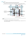
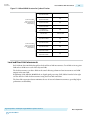

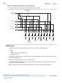
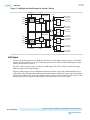
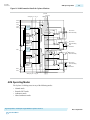
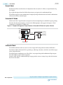
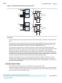


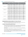
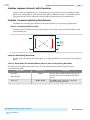
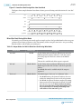
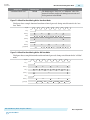
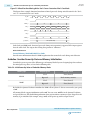
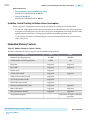

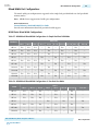
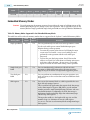
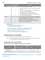
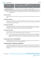


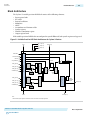

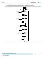
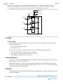
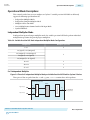
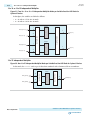
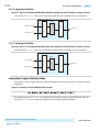


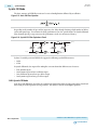
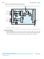
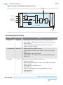


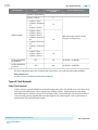
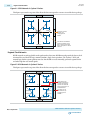
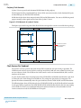
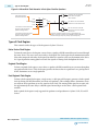


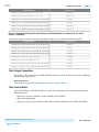
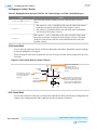
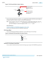
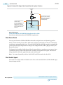
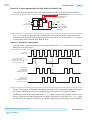

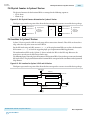
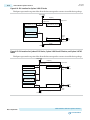
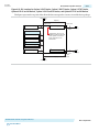
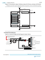
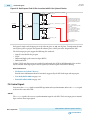


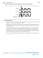


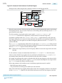
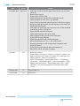


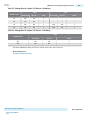
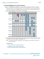
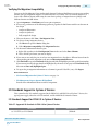


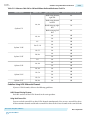
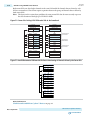


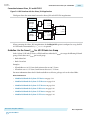


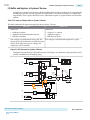

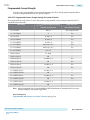
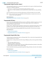
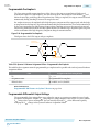
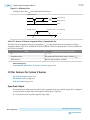
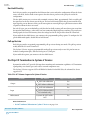

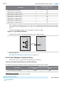
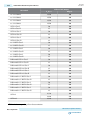


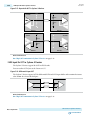
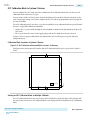
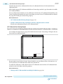
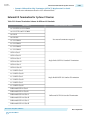
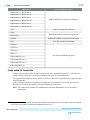
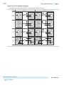
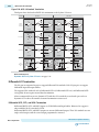

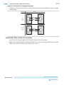
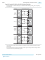
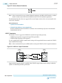

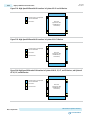

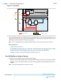
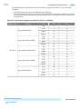
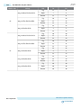

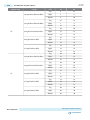


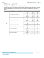
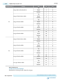
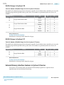
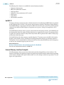
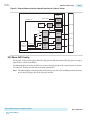
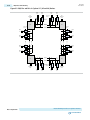
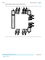
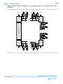
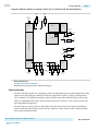
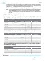
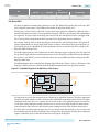
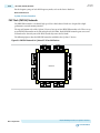

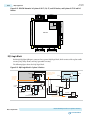
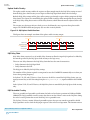


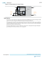

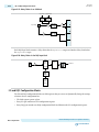

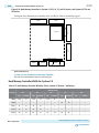


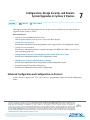
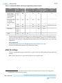
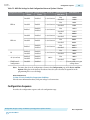

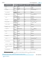

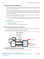
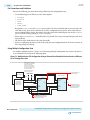
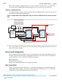
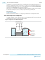
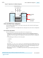
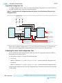

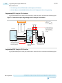

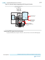

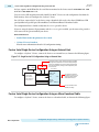


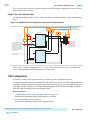


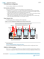
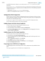
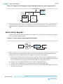
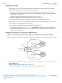


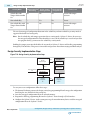
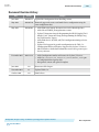


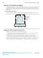


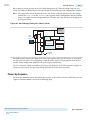
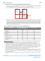
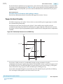
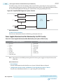
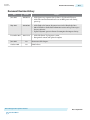


![取扱説明書 [F-01C] - Altehandys.de](http://vs1.manualzilla.com/store/data/006698700_2-1423e4aa8845601d17d5495c0fe871e1-150x150.png)