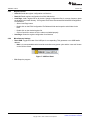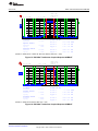
1
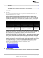
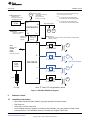
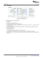
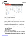
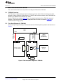
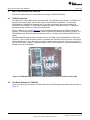
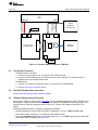
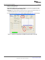
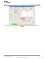
User's Guide
SLAU432 – February 2012
DAC348x EVM
1
2
3
4
5
Contents
Introduction .................................................................................................................. 2
1.1
Overview ............................................................................................................ 2
1.2
EVM Block Diagram ............................................................................................... 2
Software Control ............................................................................................................ 3
2.1
Installation Instructions ............................................................................................ 3
2.2
Software Operation ................................................................................................ 4
Basic Test Procedure with TSW1400 ................................................................................... 11
3.1
TSW1400 Overview .............................................................................................. 11
3.2
Test Block Diagram for TSW1400 .............................................................................. 11
3.3
Test Setup Connection .......................................................................................... 12
3.4
DAC348x Example Setup Procedure .......................................................................... 12
3.5
TSW1400 Example Setup Procedure .......................................................................... 13
Basic Test Procedure with TSW3100 ................................................................................... 16
4.1
TSW3100 Overview .............................................................................................. 16
4.2
Test Block Diagram for TSW3100 .............................................................................. 16
4.3
Test Set-up Connection .......................................................................................... 17
4.4
DAC348x Example Setup Procedure .......................................................................... 17
4.5
TSW3100 Example Setup Procedure .......................................................................... 17
References ................................................................................................................. 20
5.1
Related Products From Texas Instruments ................................................................... 20
5.2
Related Tools From Texas Instruments ....................................................................... 20
List of Figures
1
DAC348x EVM Block Diagram ............................................................................................ 3
2
Input Control Option ........................................................................................................ 4
3
PLL Configuration ........................................................................................................... 6
4
Digital Block Options
5
Output control Options
17
.......................................................................................................
.....................................................................................................
CDCE62005 Tab Configured for 4x Interpolation.......................................................................
USB Port Reset ............................................................................................................
Test Set-up Block Diagram for TSW1400 ..............................................................................
EVM Platform Selection ..................................................................................................
Select DAC348x Devices in the High Speed Converter Pro GUI Program ........................................
Load DAC Firmware Prompt .............................................................................................
Load File to Transfer into TSW1400 ....................................................................................
DAC348x Transformer Coupled Output at 60MHz IF ................................................................
DAC348x Transformer Coupled Output at 30MHz IF ................................................................
TSW3100 FPGA Clock 100-Ω LVDS Termination at Pins T31 and T32 of the FPGA ...........................
Test Set-up Block Diagram for TSW3100 ..............................................................................
TSW3100 CommSignalPattern (WCDMA) Programming GUI for DAC3484 ......................................
18
TSW3100 CommSignalPattern (WCDMA) Programming GUI for DAC3482, DAC34H84, and
6
7
8
9
10
11
12
13
14
15
16
SLAU432 – February 2012
Submit Documentation Feedback
DAC348x EVM
Copyright © 2012, Texas Instruments Incorporated
7
8
9
10
11
12
13
13
14
15
15
16
17
18
1
Introduction
www.ti.com
DAC34SH84................................................................................................................ 19
List of Tables
1
DAC348xEVM Jumpers: (make sure the following jumpers are at their default setting) ......................... 12
1
Introduction
1.1
Overview
This document is intended to serve as a basic user’s guide for the DAC3484/2 EVM Revision F, and
DAC34H84/SH84 EVM revision C and above.
The Texas Instruments DAC348x evaluation module (EVM) is a family of circuit boards that allows
designers to evaluate the performance of Texas Instruments' DAC348x family of digital-to-analog
converters (DAC). The 16-bit, ultra low power family of DACs has either 16-bit wide or 32-bit wide DDR
LVDS data input, integrated 2x/4x/8x/16x interpolation filters, 32-bit NCO, on-chip PLL, and exceptional
linearity at high IFs. The EVM provides a flexible environment to test the DAC348x under a variety of
clock, data input, and IF output conditions.
DAC3484
DAC3482
DAC34H84
DAC34SH84
Output Channel
4
2
4
4
EVM Part No.
DAC348x Rev. F
DAC348x Rev. F
DAC34H84 Rev. C
DAC34H84 Rev. C
Maximum DAC Rate
1.25GSPS
1.25GSPS
1.25GSPS
1.5GSPS
Digital Interface
16-bit LVDS Interface
16-bit LVDS Interface
32-bit LVDS Interface
32-bit LVDS Interface
Maximum Data Rate per Channel
312.5MSPS
625MSPS
625MSPS
750MSPS
Maximum LVDS Bus Toggle Rate
1.25GSPS
1.25GSPS
1.25GSPS
1.5GSPS
Pattern Generator Support
TSW1400/TSW3100
TSW1400/TSW3100
TSW1400/TSW3100
TSW1400/TSW3100
with limited data rate
support
For ease of use as a complete IF transmit solution, the DAC348xEVM includes the Texas Instruments
CDCE62005 clock generator/jitter cleaner for clocking the DAC348x. Besides providing a high-quality, low
jitter DAC sampling clock to the DAC348x, the CDCE62005 also provides FPGA clocks to the
TSW1400EVM (or TSW3100EVM) as FPGA reference clocks.
The EVM can be used along with Texas Instruments TSW1400 or TSW3100 with limited data rate support
(up to 1.25GSPS LVDS Bus rate) to perform a wide varieties of test and measurements. The TSW1400
generates the test patterns that are fed to the DAC348x through a maximum 1.5 GSPS LVDS Bus port.
These EVM boards are also compatible with Altera® and Xilinx® FPGA development platforms for rapid
evaluation and prototyping. The on-board HSMC connector input allows direct connection to the HSMC
compatible Altera development platforms, and the externally attached FMC-DAC-Adapter board available
from TI enables the connection of the EVM to the Xilinx development platforms with FMC headers.
For evaluation of complete RF transmit solution, see the TSW308x EVM. The EVM integrates the
DAC348x, TRF3705, and LMK04800 devices into one RF transmitter system.
See the TSW308x EVM web folders at:
http://www.ti.com/tool/tsw3085evm
http://www.ti.com/tool/tsw3084evm
http://www.ti.com/tool/tsw30h84evm
http://www.ti.com/tool/tsw30sh84evm
1.2
EVM Block Diagram
Figure 1 shows the configuration of the EVM with the TSW1400 or TSW3100 used for pattern generation.
2
DAC348x EVM
Copyright © 2012, Texas Instruments Incorporated
SLAU432 – February 2012
Submit Documentation Feedback
Software Control
www.ti.com
J9
19.2MHz Reference
·
·
LVCMOS Level
Secondary Reference for
CDCE62005 PLL Mode
Ext. CLK Input
·
·
·
·
1.3Vp Single Ended Max
1.5GHz Max
Primary Reference
(LVPECL AC coupled )
PRI
19.2MHz
TCXO
SEC
Y4
Ext. CLK Output
Clock routing is optimized for layout depending
on the clock input pin out location.
YA* =
·
Y1 for DAC3484 and DAC3482 EVMs
·
Y2 for DAC34H84 and DAC34SH84 EVMs
YB* =
·
Y2 for DAC3484 and DAC3482 EVMs
·
Y1 for DAC34H84 and DAC34SH84 EVMs
CDCE62005
·
·
J10
Y3
FPGA CLK
TSW3100 or TSW1400
LVDS AC coupled
YB*
J11
YA*
OSTR_CLK
DAC_CLK
FPGA CLK 2
(LVPECL AC
Coupled)
(LVPECL AC
Coupled)
·
·
Required for TSW1400 interface with DAC34H84 and DAC34SH84
LVDS AC coupled
+
A
DATA
DATA _CLK
FRAME
SYNC
PARITY
5th Order LPF
(LVDS DC Coupled)
5th Order LPF
Power
Supply
Circuits
_
+
B
J7
DAC348X
_
C
+
J6
DAC3482 Outputs
J3
5th Order LPF
_
J18
+
D
J2
5th Order LPF
_
6V Only
Note: 5th Order LPF is bypassed by default
Figure 1. DAC348x EVM Block Diagram
2
Software Control
2.1
Installation Instructions
•
•
•
•
Open folder named DAC348x_Installer_vxpx (xpx represents the latest version)
Run Setup.exe
Follow the on-screen instructions
Once installed, launch the program by clicking on the DAC348x_GUI_vxpx program in Start>Texas
Instruments DACs. The installation directory is located at C:\Program Files\Texas
SLAU432 – February 2012
Submit Documentation Feedback
DAC348x EVM
Copyright © 2012, Texas Instruments Incorporated
3
Software Control
•
2.2
www.ti.com
Instruments\DAC348x
When plugging in the USB cable for the first time, you will be prompted to install the USB drivers.
– When a pop-up screen opens, select “Continue Downloading”.
– Follow the on screen instructions to install the USB drivers
– If needed, you can access the drivers directly in the install directory
Software Operation
The software allows programming control of the DAC device and the CDC device. The front panel
provides a tab for full programming of each device. The GUI tabs provide more convenient and simplified
interface to the most used registers of each device.
Each device, including the DAC3484, DAC3482, and DAC34H84/SH84, has its own custom control
interface. At the top level of the GUI are five control tabs. The first four are used to configure the DAC348x
and the last for the CDCE62005.
2.2.1
Input Control Options
Figure 2. Input Control Option
•
•
•
•
•
•
•
•
4
FIFO: allows the configuration of the FIFO and FIFO synchronization (sync) sources.
LVDS delay: provides internal delay of either the LVDS DATA or LVDS DATACLK to help meet the
input setup/hold time.
Data Routing: provides flexible routing of the A, B, C, and D sample input data to the appropriate
digital path.
Note: the DAC3482 does not support this mode
SIF Control: provides control of the Serial Interface (3-wires or 4-wires) and Serial Interface Sync
(SIF Sync).
Input Format: provides control of the input data format (i.e., 2s complement or offset binary)
Parity: provides configuration of the parity input.
PLL Settings: provides configuration of the on-chip PLL circuitry.
Temperature Sensor: provides temperature monitoring of DAC3484/2 die temperature.
DAC348x EVM
Copyright © 2012, Texas Instruments Incorporated
SLAU432 – February 2012
Submit Documentation Feedback
Software Control
www.ti.com
2.2.1.1
FIFO Settings
The DAC348x has 8-samples deep FIFO to relax the timing requirement of a typical transmitter system.
The FIFO has an input pointer and an output pointer, and both pointers can accept various input sources
as reset triggers of input and output pointer position. One important application for input and output pointer
control is the ability to synchronize multiple DACs in the system. For additional information, see the
relevant DAC348x data sheet.
• FIFO Offset: The default position of FIFO output pointer after reset by the synchronization source. This
setting can be used to change the latency of the DAC348x.
• Data Formatter Sync (DAC3482 and DAC3484): Synchronization source for FIFO data formatter.
Select between LVDS FRAME or LVDS SYNC signals.
• FIFO Sync Select (DAC34H84 and DAC34SH84): Select the internal digital routing of LVDS ISTR or
LVDS SYNC to the FIFO ISTR path
• FIFO Input Sync: Synchronization source for FIFO input pointer. Select among the LVDS FRAME
(ISTR), LVDS SYNC, and/or SPI register SIF-SYNC to reset the FIFO input pointer position.
• FIFO Output Sync: Synchronization source for FIFO output pointer. Select among the LVDS FRAME
(ISTR), LVDS SYNC, SPI register SIF-SYNC, and/or OSTR signal to reset the FIFO output pointer
position.
– For single device application without the need for precise latency control, Single Sync Source Mode
may be used. The FIFO output pointer position can be reset with LVDS FRAME (ISTR), LVDS
SYNC, and/or SPI register SIF-SYNC. See the Single Sync Source Mode in the relevant DAC348x
data sheet for details.
– For multiple device synchronization, select the OSTR signal as the FIFO output synchronization
source. If the DAC is configured to accept external DAC Clock input, then the OSTR signal is the
external LVPECL signal to the OSTRP/N pins. If the DAC is configured to accept the internal
on-chip PLL clock, then the OSTR signal is the internally generated PFD frequency. See the Dual
Sync Sources Mode in the relevant DAC348x data sheet for details.
2.2.1.2
LVDS Delay Settings
Depending on the signal source implementation (i.e. TSW1400, TSW3100, or FPGA System), the
following options can be implemented to meet the minimum setup and hold time of DAC348x data
latching:
• Set the on-chip LVDS DATA or DATACLOCK delay: The DAC348x includes on-chip LVDS DATA or
DATACLK delay. The delay ranges from 0ps to 280ps with an approximate 40ps step. This LVDS
DATACLOCK delay does not account for additional PCB trace-to-trace delay variation, only the internal
DATACLK delay.
– The TSW1400 pattern generator sends out LVDS DATA and DATACLK as center aligned signal.
Additional DATACLK delay is not needed.
– The TSW3100 pattern generator sends out LVDS DATA and DATACLK as edge-aligned signal.
Typical setting of 160ps or more will help meet the timing requirement for most of the TSW3100 +
DAC348x EVM setup.
• Modify the external LVDS DATACLK PCB trace delay: Additional trace length on the bottom side of the
PCB can be added to the LVDS DATACLK PCB trace length. Set SJP9, SJP10, SJP11, and SJP12 to
2-3 position for approximately 220ps of trace delay.
SLAU432 – February 2012
Submit Documentation Feedback
DAC348x EVM
Copyright © 2012, Texas Instruments Incorporated
5
Software Control
2.2.1.3
www.ti.com
PLL Settings
Figure 3. PLL Configuration
Follow the steps below to configure the PLL.
1. Enable PLL
2. Uncheck PLL reset and PLL sleep
3. Set M and N ratio such that FDAC = (M)/(N) x Fref
4. For the DAC3482, DAC3484, and DAC34H84: Set the prescaler such that the FDAC x prescaler is within
3.3GHz and 4GHz.
5. For the DAC34SH84, Set the prescaler such that the FDAC x prescaler is within 2.7GHz and 3.3GHz.
6. Set VCO Bias Tune to “1”
7. Charge Pump setting
(a) If stability (P x M) is less than 120, then set to “Single”.
(b) If stability (P x M) is greater than 120, then set to “Double” or install external loop filter
8. Adjust the Freq. Tune (coarse tune) accordingly. For additional information, see the relevant DAC348x
data sheet.
6
DAC348x EVM
Copyright © 2012, Texas Instruments Incorporated
SLAU432 – February 2012
Submit Documentation Feedback
Software Control
www.ti.com
2.2.2
Digital Block Options
Figure 4. Digital Block Options
•
•
•
•
•
•
•
•
Interpolation: allows control of the data rate versus DAC sampling rate ratio
(i.e. data rate x interpolation = DAC sampling rate).
Digital Mixer: allows control of the coarse mixer function.
Note: If fine mixer (NCO) is used, the “ Enable Mixer” button must be checked, and the coarse
mixer must be bypassed. See the following NCO bullet for detail.
Inverse sinx/x filter: allows compensation of the sinx/x attenuation of the DAC output.
Note: If inverse sinx/x filter is used, the input data digital full-scale must be backed off
accordingly to avoid digital saturation.
Clock Receiver Sleep: allows the DAC clock receiver to be in sleep mode. The DAC has minimum
power consumption in this mode.
Clock Divider Sync: allows the synchronization of the internal divided-down clocks using either
FRAME, SYNC, or OSTR signal. Enable the divider sync as part of the initialization procedure or
resynchronization procedure.
Group Delay: allows adjustment of group delay for each I/Q channel. This is useful for wideband
sideband suppression. Note: This feature is not available for the DAC34SH84.
Offset Adjustment: allows adjustment of dc offset to minimize the LO feed-through of the modulator
output. This section requires syncing for proper operation. The synchronization options are listed
below:
– REGWR: auto-sync from SIF register write. If this option is chosen, the GUI automatically
synchronizes the offset adjustment with each value update by writing to 0x08 (offset A) or
0x0A (offset B) registers last.
– OSTR: sync from the external LVPECL OSTR signal. Clock divider sync must be enabled with
OSTR set as sync source
– SYNC: sync from the external LVDS SYNC signal.
– SIF SYNC: sync from SIF Sync. Uncheck and check the SIF Sync button for sync event.
QMC Adjustment: allows adjustment of the gain and phase of the I/Q channel to minimize sideband
power of the modulator output.
– REGWR: auto-sync from SIF register write. If this option is chosen, the GUI automatically
synchronizes the offset adjustment with each value update by writing to 0x10 (QMC phase
AB) or 0x11 (QMC phase CD) registers last.
SLAU432 – February 2012
Submit Documentation Feedback
DAC348x EVM
Copyright © 2012, Texas Instruments Incorporated
7
Software Control
•
2.2.3
www.ti.com
– OSTR: sync from the external LVPECL OSTR signal. Clock divider sync must be enabled with
OSTR set as sync source.
– SYNC: sync from the external LVDS SYNC signal.
– SIF SYNC: sync from SIF Sync. Uncheck and check the SIF Sync button for sync event.
NCO: allows fine mixing of the I/Q signal. The procedure to adjust the NCO mixing frequency are listed
below:
1. Enter the DAC sampling frequency in Fsample.
2. Enter the desired mixing frequency in both NCO freq_AB and NCO freq_CD.
3. Press Update freq
4. Sync the NCO block from the following options:
• REGWR: auto-sync from SIF register write. Writing to either Phase OffsetAB or Phase
OffsetCD can create a sync event.
• OSTR: sync from the external LVPECL OSTR signal. Clock divider sync must be enabled with
OSTR set as sync source. Refer to the datasheet for OSTR period requirement.
• SYNC: sync from the external SYNC signal
• SIF SYNC: sync from SIF Sync. Uncheck and check the SIF Sync button for sync event.
Output Control Options
Figure 5. Output control Options
•
•
•
•
8
Output Options: allows the configuration of reference, output polarity, and output delay
Data Routing: provides flexible routing of the A, B, C, and D digital path to the desired output channels.
Note: The DAC3482 does not support this mode.
DAC Gain: configures the full-scale DAC current and DAC3484/DAC3482 mode. With Rbiaj resistor set
at 1.28kΩ:
– DAC Gain = 15 for 30mA full-scale current.
– DAC Gain = 10 for 20mA full-scale current (default).
Output Shutoff On: allows outputs to shut-off when DACCLK GONE, DATACLK GONE, or FIFO
COLLISION alarm event occurs.
DAC348x EVM
Copyright © 2012, Texas Instruments Incorporated
SLAU432 – February 2012
Submit Documentation Feedback
Software Control
www.ti.com
2.2.4
CDCE62005
Figure 6. CDCE62005 Tab Configured for 4x Interpolation
Clock frequency control is determined by register values in the CDCE62005 Control tab. See the
CDCE62005 data sheet for detailed explanations of the register configuration to change the clock
frequency.
The following CDCE62005 outputs are critical to proper operation of the DAC348x:
• YA*: DAC348x DAC sampling clock. This clock is an ac coupled LVPECL. If the DAC348x is
configured for internal PLL mode, this will be the reference clock input for the PLL block.
– YA* = Y1 for DAC3484 and DAC3482 EVMs
– YA* = Y2 for DAC34H84 and DAC34SH84 EVMs
• YB*: DAC348x FIFO OSTR clock. This clock is an ac coupled LVPECL. The clock rate for this should
be at least FDAC/Interpolation/8. See the DAC348x data sheet for more details.
– The whole OSTR clock equation needs to take account of both the Y1 CDCE62005 clock divider
ratio and the additional CDCP1803 divide-by-2 clock divider.
– This OSTR signal can be a slower periodic signal or a pulse depending on the application.
– Note: The FIFO OSTR clock should be disabled when the DAC348x is configured in PLL mode.
– YB* = Y2 for DAC3484 and DAC3482 EVMs
– YB* = Y1 for DAC34H84 and DAC34SH84 EVMs
• Y3: FPGA Clock 1. This clock is an ac coupled LVDS. The clock rate for this should be
– FDAC/interpolation/2 for DAC3484
– FDAC/interpolation/4 for DAC3482, DAC34H84, and DAC34SH84
• Y4: FPGA Clock 2. This clock is an ac coupled LVDS. This clock must be enabled when using the
DAC34H84 and DAC34SH84 with the TSW1400. The clock rate for this should be FDAC/interpolation/4
for DAC34H84, and DAC34SH84
SLAU432 – February 2012
Submit Documentation Feedback
DAC348x EVM
Copyright © 2012, Texas Instruments Incorporated
9
Software Control
2.2.5
www.ti.com
Register Control
Send All: Sends the register configuration to all devices
Read All: Reads register configuration from DAC348x device
Load Regs: Load a register file for all devices. Sample configuration files for common frequency plans
are located in the install directory: C:\Programs Files\Texas Instruments\DAC348x\EVM Configuration
File Released.
– Select Load Regs button.
– Double click on the EVM Configuration File Released folder and respective sub-folders for the
EVM.
– Double click on the desired register file.
– Click on Send All to ensure all of the values are loaded properly.
• Save Regs: Saves the register configuration for all devices
•
•
•
2.2.6
Miscellaneous Settings
• Reset USB: Toggle this button if the USB port is not responding. This generates a new USB handle
address
– Note: It is recommended that the board be reset after every power cycle and the “reset usb” button
on the GUI be clicked.
Figure 7. USB Port Reset
•
10
Exit: Stops the program
DAC348x EVM
Copyright © 2012, Texas Instruments Incorporated
SLAU432 – February 2012
Submit Documentation Feedback
Basic Test Procedure with TSW1400
www.ti.com
3
Basic Test Procedure with TSW1400
This section outlines the basic test procedure for testing the EVM with the TSW1400.
3.1
TSW1400 Overview
The TSW1400 is a high speed data capture and pattern generator board. When functioning as a pattern
generator, it has a maximum LVDS bus rate of 1.5 GSPS, and this allows evaluation of the DAC348x with
maximum 750 MSPS of input data rate per channel.
See the TSW1400 user’s guide (SLWU079) for more detailed explanation of the TSW1400 setup and
operation. This document assumes that the High Speed Data Converter Pro software (SLWC107) is
installed and functioning properly.
3.2
Test Block Diagram for TSW1400
The test set-up for general testing of the DAC348x with the TSW1400 pattern generation card is shown in
Figure 8.
PC
USB
J5
USB Mini-B
Cable
USB Mini-B
Cable
USB
+5V
J12
J9
J4
Signal
Generator
(CLK Source)
J14
J13
DAC348X
IF
TSW1400
Spectrum
Analyzer
J18
+6V
Figure 8. Test Set-up Block Diagram for TSW1400
SLAU432 – February 2012
Submit Documentation Feedback
DAC348x EVM
Copyright © 2012, Texas Instruments Incorporated
11
Basic Test Procedure with TSW1400
3.3
www.ti.com
Test Setup Connection
TSW1400 Pattern Generator.
1. Connect 5 V power supply to J12, 5V_IN jack of the TSW1400 EVM.
2. Connect PC’s USB port to J5 USB port of the TSW1400 EVM. The cable should be a standard A to
mini-B connector cable.
DAC348xEVM
1. Connect J13 connector of DAC348xEVM to J4 connector of TSW1400 EVM.
2. Connect 6V to the J18, Power In jack of the DAC3484 EVM.
3. Connect PC’s USB port to J14 USB port of the DAC348x EVM. The cable should be a standard A to
mini-B connector cable.
4. Provide a 1.3Vp, 1.5GHz max clock at J9, CLKIN SMA port of DAC348x EVM.
5. Connect the IF output port of J2, J3, J6, or J7 to the spectrum analyzer.
Table 1. DAC348xEVM Jumpers: (make sure the following jumpers are at their default setting)
3.4
Reference Designator
Setting
Function
JP2
1-2
DAC348x TXENABLE.
JP3
2-3
DAC348x SLEEP.
JP4
2-3
CDCE62005 Primary Input LVPECL Bias Enable.
JP5
1-2
CDCE62005 Reference Input Select.
JP6
1-2
CDCE62005 Power Down.
JP7
short
19.2MHz TCXO Enable.
JP8, JP9, JP12, JP13
short
SPI connection break point. This allows routing of SPI
connection to external system if troubleshooting is needed.
JP10
1-2
6V Input Select. Default is 6V at J18.
JP11
open
For DAC34H84/SH84 EVM only. Allows SPI and IO logic
threshold to switch among 1.8V, 2.5V, or 3.3V.
SJP9, SJP10, SJP11, SJP12
1-2
DAC348x DATACLK delay. Default is zero trace delay.
DAC348x Example Setup Procedure
1.
2.
3.
4.
Provide the clock input 1228.8 MHz at 1.5Vrms at J9 SMA Connector of the DAC348x EVM.
Turn on power to the board and press the reset SW1 button on the EVM
Press the “Reset USB Port” button in GUI and verify USB communication.
Select the appropriate EVM platform on the software menu.
Figure 9. EVM Platform Selection
5. Click “LOAD REGS”, browse to the installation folder and load example file
“DAC3484_FDAC_1228p8MHz_4xint_NCO_30MHz_QMCon.txt”. This file contains settings for 4x
interpolation with the DAC3484 running at 1228.8MSPS. Load this file and wait a couple of seconds for
the settings to go into effect. The DAC3482, DAC34H84, and DAC34SH84 equivalent example files
are also available in the installation folder.
12
DAC348x EVM
Copyright © 2012, Texas Instruments Incorporated
SLAU432 – February 2012
Submit Documentation Feedback
Basic Test Procedure with TSW1400
www.ti.com
3.5
TSW1400 Example Setup Procedure
1. Start the High Speed Converter Pro GUI program. When the program starts, select the DAC tab and
then select the corresponding device in the “Select DAC” menu.
Figure 10. Select DAC348x Devices in the High Speed Converter Pro GUI Program
2. When prompted Load DAC Firmware?, select YES.
Figure 11. Load DAC Firmware Prompt
3. Click on the button labeled “Load File to transfer into TSW 1400”, located near the top left of the GUI.
SLAU432 – February 2012
Submit Documentation Feedback
DAC348x EVM
Copyright © 2012, Texas Instruments Incorporated
13
Basic Test Procedure with TSW1400
www.ti.com
Figure 12. Load File to Transfer into TSW1400
4. Select the file "WCDMA_TM1_complexIF30MHz_Fdata307.2MHz_1000.tsw" under C:\Program
Files\Texas Instruments\High Speed Data Converter Pro\1400 Details\Testfiles. The data rate of the
file selected will depend on the sampling rate and interpolation ratio of the DAC configuration.
5. Enter 307.2M for the "Data Rate" and 2's complement for the "DAC Option".
6. Select Hanning for "Window".
7. In the “DAC Selection” panel on the left side of the GUI, click on “Send” to load the data into memory.
8. Toggle the SIF SYNC button of the DAC348x EVM GUI to synchronize the appropriate digital
blocks, if the example file with NCO setting is used.
9. Verify the spectrum using the Spectrum Analyzer at the four IF outputs of the DAC348x EVM (J7, J6,
J3, and J2).
• For the DAC3482 EVM, the IF outputs are at the J6 and J3 SMA connector
10. The expect results are shown in Figure 13 (NCO enabled at 30MHz) and Figure 14 (NCO disabled).
14
DAC348x EVM
Copyright © 2012, Texas Instruments Incorporated
SLAU432 – February 2012
Submit Documentation Feedback
Basic Test Procedure with TSW1400
www.ti.com
Ref -15.6 dBm
-20
* Att
* RBW 30 kHz
* VBW 300 kHz
* SWT 2 s
5 dB
PO S - 15. 587 dB m
-30
B
-40
1 RM *
CLRWR
-50
-60
-70
-80
NOR
-90
-100
-110
Center
60 MHz
2.55 MHz/
Tx Cha nne l
Ban dwi dth
3. 84 MHz
Adj ace nt Cha nne l
Ban dwi dth
W-C DMA 3G PP FWD
P ow e r
- 10 .5 8
d Bm
3. 84 MHz
L ow e r
- 78 .1 6
dB
5 MHz
U pp e r
- 76 .1 4
dB
3. 84 MHz
L ow e r
- 84 .3 1
dB
10 MHz
U pp e r
- 83 .3 7
dB
Spa cin g
Alt ern ate Ch ann el
Ban dwi dth
Span 25.5 MHz
Spa cin g
(baseband = 30MHz, NCO = 30MHz with NCO Gain disabled, QMC Gain = 1446)
Figure 13. DAC348x Transformer Coupled Output at 60MHz IF
Ref -12.3 dBm
* Att
* RBW 30 kHz
* VBW 300 kHz
* SWT 2 s
10 dB
PO S - 12. 321 dB m
-20
-30
B
-40
1 RM *
CLRWR
-50
-60
-70
-80
NOR
-90
-100
-110
Center
30 MHz
2.55 MHz/
Tx Cha nne l
Ban dwi dth
3. 84 MHz
Adj ace nt Cha nne l
Ban dwi dth
Spa cin g
P ow e r
-7 .5 2
3. 84 MHz
L ow e r
- 78 .9 5
dB
5 MHz
U pp e r
- 78 .0 4
dB
L ow e r
- 84 .0 6
dB
U pp e r
- 82 .9 7
dB
Alt ern ate Ch ann el
Ban dwi dth
Spa cin g
Span 25.5 MHz
W-C DMA 3G PP FWD
3. 84 MHz
10 MHz
d Bm
(baseband = 30MHz, NCO disabled, QMC Gain = 1024)
Figure 14. DAC348x Transformer Coupled Output at 30MHz IF
SLAU432 – February 2012
Submit Documentation Feedback
DAC348x EVM
Copyright © 2012, Texas Instruments Incorporated
15
Basic Test Procedure with TSW3100
4
www.ti.com
Basic Test Procedure with TSW3100
This section outlines the basic test procedure for testing the EVM with TSW3100.
4.1
TSW3100 Overview
The TSW3100 is a high speed pattern generator board. The LVDS Bus rate is limited to 1.25GSPS, and
this limits the maximum input data rate per channel of DAC34SH84 to 625MSPS. To evaluate the
DAC34SH84 at 1.5GSPS DAC sampling rate, 4x or higher interpolation filter must be enabled. To
evaluate the DAC34SH84 at 1.5GSPS DAC sampling rate with 2x interpolation filter (i.e. 750MSPS of
input data rate per channel), the TSW1400 must be used.
See the TSW3100 user’s guide (SLLU101) for more detailed explanations of the TSW3100 setup and
operation. This document assumes that the TSW3100 software is installed and functioning properly. The
TSW30SH84 needs TSW3100 operating software version 2.5 or higher with TSW3100 board Rev D (or
higher).
The DAC348xEVM sends the FPGA reference clock to the FPGA of the TSW3100EVM in LVDS format.
Therefore, a 100-Ω LVDS termination resistor is needed at the TSW3100 FPGA clock input. All the latest
TSW3100EVMs from TI have the 100-Ω termination installed at the bottom side of the board on pins T31
and T32 of the FPGA. Contact TI Application Support if the 100-Ω termination is missing and assistance is
needed for the 100-Ω installation.
Figure 15. TSW3100 FPGA Clock 100-Ω LVDS Termination at Pins T31 and T32 of the FPGA
4.2
Test Block Diagram for TSW3100
The test set-up for general testing of the DAC348x with the TSW3100 pattern generation card is shown in
Figure 16.
16
DAC348x EVM
Copyright © 2012, Texas Instruments Incorporated
SLAU432 – February 2012
Submit Documentation Feedback
Basic Test Procedure with TSW3100
www.ti.com
PC
Ethernet
J13
USB Mini-B
Cable
Cross-over
Ethernet Cable
USB
+5V
J9
J9
J74
Signal
Generator
(CLK Source)
J14
J13
DAC348X
IF
TSW3100
Spectrum
Analyzer
J18
+6V
Figure 16. Test Set-up Block Diagram for TSW3100
4.3
Test Set-up Connection
•
•
4.4
TSW3100 Pattern Generator
1. Connect 5V power supply to J9, 5V_IN jack of the TSW3100 EVM.
2. Connect the PC’s Ethernet port to J13, Ethernet port of the TSW3100. The cable should be a
standard cross-over Cat5e Ethernet cable.
DAC348x EVM
1. Connect J13 connector of DAC348x EVM to J74 connector of TSW3100EVM.
2. See the Test Setup Connection section.
DAC348x Example Setup Procedure
See the DAC348x Example Setup Procedure section.
4.5
TSW3100 Example Setup Procedure
Reference the TSW3100 User’s Guide (SLWU079) for more detailed explanations of the TSW3100 set-up
and operation. This document assumes the TSW3100 software is installed and functioning properly. The
DAC348x needs TSW3100 operating software version 2.5 or higher with TSW3100 board Rev D (or
higher).
CommsSignalPattern Setup from Default Configuration (WCDMA)
• Change Interpolation value to DAC Clock Rate / Interpolation / 3.84 (i.e. 1228.8 / 4/ 3.84 = 80)
• Enter desired Offset Frequency (i.e. 30 MHz) for each desired carrier
• Select the 16b QDAC output button for DAC3484 (see Figure 17) or LVDS output button for DAC3482,
DAC34H84, and DAC34SH84 (see Figure 18).
SLAU432 – February 2012
Submit Documentation Feedback
DAC348x EVM
Copyright © 2012, Texas Instruments Incorporated
17
Basic Test Procedure with TSW3100
•
•
•
•
•
www.ti.com
Check the “LOAD and Run” box
Press the green“Create” button
Toggle the SIF SYNC button of the DAC348x EVM GUI to synchronize the appropriate digital
blocks, if the example file with NCO setting is used.
Verify the spectrum using the Spectrum Analyzer at the four IF outputs of the DAC348x EVM (J7, J6,
J3, and J2).
– For the DAC3482 EVM, the IF outputs are at the J6 and J3 SMA connector
The expect results are shown in Figure 13 (NCO enabled at 30MHz) and Figure 14 (NCO disabled).
Figure 17. TSW3100 CommSignalPattern (WCDMA) Programming GUI for DAC3484
18
DAC348x EVM
Copyright © 2012, Texas Instruments Incorporated
SLAU432 – February 2012
Submit Documentation Feedback
Basic Test Procedure with TSW3100
www.ti.com
Figure 18. TSW3100 CommSignalPattern (WCDMA) Programming GUI for DAC3482, DAC34H84, and
DAC34SH84
SLAU432 – February 2012
Submit Documentation Feedback
DAC348x EVM
Copyright © 2012, Texas Instruments Incorporated
19
References
www.ti.com
5
References
5.1
Related Products From Texas Instruments
Dual-Channel, 16-Bit, 1.25 GSPS Digital-To-Analog Converter (DAC), DAC3482 (SLAS748)
Quad-Channel, 16-Bit, 1.25 GSPS Digital-To-Analog Converter (DAC), DAC3484 (SLAS749)
Quad-Channel, 16-Bit, 1.25 GSPS Digital-To-Analog Converter (DAC), DAC34H84 (SLAS751)
Quad-Channel, 16-Bit, 1.5 GSPS Digital-to-Analog Converter (DAC) , DAC34SH84 (SLAS808)
Five/Ten Output Clock Generator/Jitter Cleaner With Integrated Dual VCO, CDCE62005 (SCAS862)
5.2
Related Tools From Texas Instruments
TSW1400 High Speed Data Capture/Pattern Generator Card (SLWU079)
TSW3100 High Speed Digital Pattern Generator (SLUU101)
FMC-DAC-ADAPTER Physical Design Database Rev D Board (SLOR102)
DAC34H84EVM Design Package board rev C (SLAC518)
DAC348x EVM Software (SLAC483)
High Speed Data Converter Pro software (SLWC107)
20
DAC348x EVM
Copyright © 2012, Texas Instruments Incorporated
SLAU432 – February 2012
Submit Documentation Feedback
EVALUATION BOARD/KIT/MODULE (EVM) ADDITIONAL TERMS
Texas Instruments (TI) provides the enclosed Evaluation Board/Kit/Module (EVM) under the following conditions:
The user assumes all responsibility and liability for proper and safe handling of the goods. Further, the user indemnifies TI from all
claims arising from the handling or use of the goods.
Should this evaluation board/kit not meet the specifications indicated in the User’s Guide, the board/ kit may be returned within 30
days from the date of delivery for a full refund. THE FOREGOING LIMITED WARRANTY IS THE EXCLUSIVE WARRANTY MADE
BY SELLER TO BUYER AND IS IN LIEU OF ALL OTHER WARRANTIES, EXPRESSED, IMPLIED, OR STATUTORY,
INCLUDING ANY WARRANTY OF MERCHANTABILITY OR FITNESS FOR ANY PARTICULAR PURPOSE. EXCEPT TO THE
EXTENT OF THE INDEMNITY SET FORTH ABOVE, NEITHER PARTY SHALL BE LIABLE TO THE OTHER FOR ANY
INDIRECT, SPECIAL, INCIDENTAL, OR CONSEQUENTIAL DAMAGES.
Please read the User's Guide and, specifically, the Warnings and Restrictions notice in the User's Guide prior to handling the
product. This notice contains important safety information about temperatures and voltages. For additional information on TI's
environmental and/or safety programs, please visit www.ti.com/esh or contact TI.
No license is granted under any patent right or other intellectual property right of TI covering or relating to any machine, process, or
combination in which such TI products or services might be or are used. TI currently deals with a variety of customers for products,
and therefore our arrangement with the user is not exclusive. TI assumes no liability for applications assistance, customer product
design, software performance, or infringement of patents or services described herein.
REGULATORY COMPLIANCE INFORMATION
As noted in the EVM User’s Guide and/or EVM itself, this EVM and/or accompanying hardware may or may not be subject to the
Federal Communications Commission (FCC) and Industry Canada (IC) rules.
For EVMs not subject to the above rules, this evaluation board/kit/module is intended for use for ENGINEERING DEVELOPMENT,
DEMONSTRATION OR EVALUATION PURPOSES ONLY and is not considered by TI to be a finished end product fit for general
consumer use. It generates, uses, and can radiate radio frequency energy and has not been tested for compliance with the limits of
computing devices pursuant to part 15 of FCC or ICES-003 rules, which are designed to provide reasonable protection against
radio frequency interference. Operation of the equipment may cause interference with radio communications, in which case the
user at his own expense will be required to take whatever measures may be required to correct this interference.
General Statement for EVMs including a radio
User Power/Frequency Use Obligations: This radio is intended for development/professional use only in legally allocated frequency
and power limits. Any use of radio frequencies and/or power availability of this EVM and its development application(s) must
comply with local laws governing radio spectrum allocation and power limits for this evaluation module. It is the user’s sole
responsibility to only operate this radio in legally acceptable frequency space and within legally mandated power limitations. Any
exceptions to this is strictly prohibited and unauthorized by Texas Instruments unless user has obtained appropriate
experimental/development licenses from local regulatory authorities, which is responsibility of user including its acceptable
authorization.
For EVMs annotated as FCC – FEDERAL COMMUNICATIONS COMMISSION Part 15 Compliant
Caution
This device complies with part 15 of the FCC Rules. Operation is subject to the following two conditions: (1) This device may not
cause harmful interference, and (2) this device must accept any interference received, including interference that may cause
undesired operation
Changes or modifications not expressly approved by the party responsible for compliance could void the user's authority to operate
the equipment.
FCC Interference Statement for Class A EVM devices
This equipment has been tested and found to comply with the limits for a Class A digital device, pursuant to part 15 of the FCC
Rules. These limits are designed to provide reasonable protection against harmful interference when the equipment is operated in
a commercial environment. This equipment generates, uses, and can radiate radio frequency energy and, if not installed and used
in accordance with the instruction manual, may cause harmful interference to radio communications. Operation of this equipment in
a residential area is likely to cause harmful interference in which case the user will be required to correct the interference at his
own expense.
REGULATORY COMPLIANCE INFORMATION (continued)
FCC Interference Statement for Class B EVM devices
This equipment has been tested and found to comply with the limits for a Class B digital device, pursuant to part 15 of the FCC
Rules. These limits are designed to provide reasonable protection against harmful interference in a residential installation. This
equipment generates, uses and can radiate radio frequency energy and, if not installed and used in accordance with the
instructions, may cause harmful interference to radio communications. However, there is no guarantee that interference will not
occur in a particular installation. If this equipment does cause harmful interference to radio or television reception, which can be
determined by turning the equipment off and on, the user is encouraged to try to correct the interference by one or more of the
following measures:
• Reorient or relocate the receiving antenna.
• Increase the separation between the equipment and receiver.
• Connect the equipment into an outlet on a circuit different from that to which the receiver is connected.
• Consult the dealer or an experienced radio/TV technician for help.
For EVMs annotated as IC – INDUSTRY CANADA Compliant
This Class A or B digital apparatus complies with Canadian ICES-003.
Changes or modifications not expressly approved by the party responsible for compliance could void the user’s authority to operate
the equipment.
Concerning EVMs including radio transmitters
This device complies with Industry Canada licence-exempt RSS standard(s). Operation is subject to the following two conditions:
(1) this device may not cause interference, and (2) this device must accept any interference, including interference that may cause
undesired operation of the device.
Concerning EVMs including detachable antennas
Under Industry Canada regulations, this radio transmitter may only operate using an antenna of a type and maximum (or lesser)
gain approved for the transmitter by Industry Canada. To reduce potential radio interference to other users, the antenna type and
its gain should be so chosen that the equivalent isotropically radiated power (e.i.r.p.) is not more than that necessary for successful
communication.
This radio transmitter has been approved by Industry Canada to operate with the antenna types listed in the user guide with the
maximum permissible gain and required antenna impedance for each antenna type indicated. Antenna types not included in this
list, having a gain greater than the maximum gain indicated for that type, are strictly prohibited for use with this device.
Cet appareil numérique de la classe A ou B est conforme à la norme NMB-003 du Canada.
Les changements ou les modifications pas expressément approuvés par la partie responsable de la conformité ont pu vider
l’autorité de l'utilisateur pour actionner l'équipement.
Concernant les EVMs avec appareils radio
Le présent appareil est conforme aux CNR d'Industrie Canada applicables aux appareils radio exempts de licence. L'exploitation
est autorisée aux deux conditions suivantes : (1) l'appareil ne doit pas produire de brouillage, et (2) l'utilisateur de l'appareil doit
accepter tout brouillage radioélectrique subi, même si le brouillage est susceptible d'en compromettre le fonctionnement.
Concernant les EVMs avec antennes détachables
Conformément à la réglementation d'Industrie Canada, le présent émetteur radio peut fonctionner avec une antenne d'un type et
d'un gain maximal (ou inférieur) approuvé pour l'émetteur par Industrie Canada. Dans le but de réduire les risques de brouillage
radioélectrique à l'intention des autres utilisateurs, il faut choisir le type d'antenne et son gain de sorte que la puissance isotrope
rayonnée équivalente (p.i.r.e.) ne dépasse pas l'intensité nécessaire à l'établissement d'une communication satisfaisante.
Le présent émetteur radio a été approuvé par Industrie Canada pour fonctionner avec les types d'antenne énumérés dans le
manuel d’usage et ayant un gain admissible maximal et l'impédance requise pour chaque type d'antenne. Les types d'antenne non
inclus dans cette liste, ou dont le gain est supérieur au gain maximal indiqué, sont strictement interdits pour l'exploitation de
l'émetteur.
【Important Notice for Users of this Product in Japan】
This development kit is NOT certified as Confirming to Technical Regulations of Radio Law of Japan
If you use this product in Japan, you are required by Radio Law of Japan to follow the instructions below with respect to this
product:
1.
2.
3.
Use this product in a shielded room or any other test facility as defined in the notification #173 issued by Ministry of Internal
Affairs and Communications on March 28, 2006, based on Sub-section 1.1 of Article 6 of the Ministry’s Rule for Enforcement of
Radio Law of Japan,
Use this product only after you obtained the license of Test Radio Station as provided in Radio Law of Japan with respect to
this product, or
Use of this product only after you obtained the Technical Regulations Conformity Certification as provided in Radio Law of
Japan with respect to this product. Also, please do not transfer this product, unless you give the same notice above to the
transferee. Please note that if you could not follow the instructions above, you will be subject to penalties of Radio Law of
Japan.
Texas Instruments Japan Limited
(address) 24-1, Nishi-Shinjuku 6 chome, Shinjukku-ku, Tokyo, Japan
http://www.tij.co.jp
【ご使用にあたっての注】
本開発キットは技術基準適合証明を受けておりません。
本製品のご使用に際しては、電波法遵守のため、以下のいずれかの措置を取っていただく必要がありますのでご注意ください。
1.
2.
3.
電波法施行規則第6条第1項第1号に基づく平成18年3月28日総務省告示第173号で定められた電波暗室等の試験設備でご使用い
ただく。
実験局の免許を取得後ご使用いただく。
技術基準適合証明を取得後ご使用いただく。
なお、本製品は、上記の「ご使用にあたっての注意」を譲渡先、移転先に通知しない限り、譲渡、移転できないものとします。
上記を遵守頂けない場合は、電波法の罰則が適用される可能性があることをご留意ください。
日本テキサス・インスツルメンツ株式会社
東京都新宿区西新宿6丁目24番1号
西新宿三井ビル
http://www.tij.co.jp
SPACER
SPACER
SPACER
SPACER
SPACER
SPACER
SPACER
SPACER
SPACER
SPACER
SPACER
SPACER
SPACER
SPACER
SPACER
SPACER
EVALUATION BOARD/KIT/MODULE (EVM)
WARNINGS, RESTRICTIONS AND DISCLAIMERS
For Feasibility Evaluation Only, in Laboratory/Development Environments. Unless otherwise indicated, this EVM is not a
finished electrical equipment and not intended for consumer use. It is intended solely for use for preliminary feasibility evaluation in
laboratory/development environments by technically qualified electronics experts who are familiar with the dangers and application
risks associated with handling electrical mechanical components, systems and subsystems. It should not be used as all or part of a
finished end product.
Your Sole Responsibility and Risk. You acknowledge, represent and agree that:
1.
2.
3.
4.
You have unique knowledge concerning Federal, State and local regulatory requirements (including but not limited to Food and
Drug Administration regulations, if applicable) which relate to your products and which relate to your use (and/or that of your
employees, affiliates, contractors or designees) of the EVM for evaluation, testing and other purposes.
You have full and exclusive responsibility to assure the safety and compliance of your products with all such laws and other
applicable regulatory requirements, and also to assure the safety of any activities to be conducted by you and/or your
employees, affiliates, contractors or designees, using the EVM. Further, you are responsible to assure that any interfaces
(electronic and/or mechanical) between the EVM and any human body are designed with suitable isolation and means to safely
limit accessible leakage currents to minimize the risk of electrical shock hazard.
You will employ reasonable safeguards to ensure that your use of the EVM will not result in any property damage, injury or
death, even if the EVM should fail to perform as described or expected.
You will take care of proper disposal and recycling of the EVM’s electronic components and packing materials.
Certain Instructions. It is important to operate this EVM within TI’s recommended specifications and environmental considerations
per the user guidelines. Exceeding the specified EVM ratings (including but not limited to input and output voltage, current, power,
and environmental ranges) may cause property damage, personal injury or death. If there are questions concerning these ratings
please contact a TI field representative prior to connecting interface electronics including input power and intended loads. Any
loads applied outside of the specified output range may result in unintended and/or inaccurate operation and/or possible permanent
damage to the EVM and/or interface electronics. Please consult the EVM User's Guide prior to connecting any load to the EVM
output. If there is uncertainty as to the load specification, please contact a TI field representative. During normal operation, some
circuit components may have case temperatures greater than 60°C as long as the input and output are maintained at a normal
ambient operating temperature. These components include but are not limited to linear regulators, switching transistors, pass
transistors, and current sense resistors which can be identified using the EVM schematic located in the EVM User's Guide. When
placing measurement probes near these devices during normal operation, please be aware that these devices may be very warm
to the touch. As with all electronic evaluation tools, only qualified personnel knowledgeable in electronic measurement and
diagnostics normally found in development environments should use these EVMs.
Agreement to Defend, Indemnify and Hold Harmless. You agree to defend, indemnify and hold TI, its licensors and their
representatives harmless from and against any and all claims, damages, losses, expenses, costs and liabilities (collectively,
"Claims") arising out of or in connection with any use of the EVM that is not in accordance with the terms of the agreement. This
obligation shall apply whether Claims arise under law of tort or contract or any other legal theory, and even if the EVM fails to
perform as described or expected.
Safety-Critical or Life-Critical Applications. If you intend to evaluate the components for possible use in safety critical
applications (such as life support) where a failure of the TI product would reasonably be expected to cause severe personal injury
or death, such as devices which are classified as FDA Class III or similar classification, then you must specifically notify TI of such
intent and enter into a separate Assurance and Indemnity Agreement.
Mailing Address: Texas Instruments, Post Office Box 655303, Dallas, Texas 75265
Copyright © 2012, Texas Instruments Incorporated
IMPORTANT NOTICE
Texas Instruments Incorporated and its subsidiaries (TI) reserve the right to make corrections, modifications, enhancements, improvements,
and other changes to its products and services at any time and to discontinue any product or service without notice. Customers should
obtain the latest relevant information before placing orders and should verify that such information is current and complete. All products are
sold subject to TI’s terms and conditions of sale supplied at the time of order acknowledgment.
TI warrants performance of its hardware products to the specifications applicable at the time of sale in accordance with TI’s standard
warranty. Testing and other quality control techniques are used to the extent TI deems necessary to support this warranty. Except where
mandated by government requirements, testing of all parameters of each product is not necessarily performed.
TI assumes no liability for applications assistance or customer product design. Customers are responsible for their products and
applications using TI components. To minimize the risks associated with customer products and applications, customers should provide
adequate design and operating safeguards.
TI does not warrant or represent that any license, either express or implied, is granted under any TI patent right, copyright, mask work right,
or other TI intellectual property right relating to any combination, machine, or process in which TI products or services are used. Information
published by TI regarding third-party products or services does not constitute a license from TI to use such products or services or a
warranty or endorsement thereof. Use of such information may require a license from a third party under the patents or other intellectual
property of the third party, or a license from TI under the patents or other intellectual property of TI.
Reproduction of TI information in TI data books or data sheets is permissible only if reproduction is without alteration and is accompanied
by all associated warranties, conditions, limitations, and notices. Reproduction of this information with alteration is an unfair and deceptive
business practice. TI is not responsible or liable for such altered documentation. Information of third parties may be subject to additional
restrictions.
Resale of TI products or services with statements different from or beyond the parameters stated by TI for that product or service voids all
express and any implied warranties for the associated TI product or service and is an unfair and deceptive business practice. TI is not
responsible or liable for any such statements.
TI products are not authorized for use in safety-critical applications (such as life support) where a failure of the TI product would reasonably
be expected to cause severe personal injury or death, unless officers of the parties have executed an agreement specifically governing
such use. Buyers represent that they have all necessary expertise in the safety and regulatory ramifications of their applications, and
acknowledge and agree that they are solely responsible for all legal, regulatory and safety-related requirements concerning their products
and any use of TI products in such safety-critical applications, notwithstanding any applications-related information or support that may be
provided by TI. Further, Buyers must fully indemnify TI and its representatives against any damages arising out of the use of TI products in
such safety-critical applications.
TI products are neither designed nor intended for use in military/aerospace applications or environments unless the TI products are
specifically designated by TI as military-grade or "enhanced plastic." Only products designated by TI as military-grade meet military
specifications. Buyers acknowledge and agree that any such use of TI products which TI has not designated as military-grade is solely at
the Buyer's risk, and that they are solely responsible for compliance with all legal and regulatory requirements in connection with such use.
TI products are neither designed nor intended for use in automotive applications or environments unless the specific TI products are
designated by TI as compliant with ISO/TS 16949 requirements. Buyers acknowledge and agree that, if they use any non-designated
products in automotive applications, TI will not be responsible for any failure to meet such requirements.
Following are URLs where you can obtain information on other Texas Instruments products and application solutions:
Products
Applications
Audio
www.ti.com/audio
Automotive and Transportation www.ti.com/automotive
Amplifiers
amplifier.ti.com
Communications and Telecom www.ti.com/communications
Data Converters
dataconverter.ti.com
Computers and Peripherals
www.ti.com/computers
DLP® Products
www.dlp.com
Consumer Electronics
www.ti.com/consumer-apps
DSP
dsp.ti.com
Energy and Lighting
www.ti.com/energy
Clocks and Timers
www.ti.com/clocks
Industrial
www.ti.com/industrial
Interface
interface.ti.com
Medical
www.ti.com/medical
Logic
logic.ti.com
Security
www.ti.com/security
Power Mgmt
power.ti.com
Space, Avionics and Defense
www.ti.com/space-avionics-defense
Microcontrollers
microcontroller.ti.com
Video and Imaging
www.ti.com/video
RFID
www.ti-rfid.com
OMAP Mobile Processors
www.ti.com/omap
Wireless Connectivity
www.ti.com/wirelessconnectivity
TI E2E Community Home Page
e2e.ti.com
Mailing Address: Texas Instruments, Post Office Box 655303, Dallas, Texas 75265
Copyright © 2012, Texas Instruments Incorporated