1
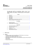
User's Guide
SBAU193A – July 2011 – Revised February 2012
ADS8568EVM-PDK
Figure 1. ADS8568EVM-PDK
This user's guide describes the characteristics, operation, and use of the ADS8568EVM by itself and as
part of the ADS8568EVM-PDK. This evaluation module (EVM) is an evaluation platform for the ADS8568,
a 16-bit, eight-channel, simultaneous sampling, bipolar input analog-to-digital converter (ADC). The
ADS8568EVM allows evaluation of all aspects of the ADS8568 device. This document includes an EVM
QuickStart, hardware and software details, bill of materials, and schematic.
ADCPro is a trademark of Texas Instruments Incorporated.
All other trademarks are the property of their respective owners.
SBAU193A – July 2011 – Revised February 2012
Submit Documentation Feedback
Copyright © 2011–2012, Texas Instruments Incorporated
ADS8568EVM-PDK
1
www.ti.com
1
2
3
4
5
6
Contents
EVM Overview ............................................................................................................... 3
QuickStart .................................................................................................................... 4
Quick Reference ............................................................................................................ 6
Using the ADS8568EVM-PDK Plug-In in ADCPro ..................................................................... 7
ADS8568EVM Hardware Details ........................................................................................ 10
Bill of Materials, Layout, and Schematic ............................................................................... 14
1
ADS8568EVM-PDK ......................................................................................................... 1
2
ADS8568EVM Default Jumper Settings
3
Operation in Hardware Mode .............................................................................................. 8
4
Operation in Software Mode ............................................................................................... 9
5
Analog Input Schematic
6
Jumpers JP16, JP18, JP21, and JP22 ................................................................................. 11
7
BVDD Voltage Selection
8
ADS8568EVM: Silkscreen (Top Layer) ................................................................................. 17
9
ADS8568EVM: Top
10
ADS8568EVM: Internal GND Layer 1 .................................................................................. 17
11
ADS8568EVM: Internal Layer 2 ......................................................................................... 17
12
ADS8568EVM: Silkscreen (Bottom Layer) ............................................................................. 17
13
ADS85x8EVM: Schematic 1 ............................................................................................. 19
14
ADS85x8EVM: Schematic 2 ............................................................................................. 20
List of Figures
.................................................................................
..................................................................................................
...................................................................................................
.......................................................................................................
4
10
13
17
List of Tables
1
Related Documents ......................................................................................................... 3
2
Default Jumper Configuration ............................................................................................. 5
3
Connector J3: Power-Supply Inputs
12
4
Analog Bipolar Input Supply Jumpers
12
5
6
7
2
....................................................................................
..................................................................................
Connector J4: Parallel Control ...........................................................................................
Connector J5: Parallel Interface Data Ouput ..........................................................................
Bill of Materials.............................................................................................................
ADS8568EVM-PDK
14
14
15
SBAU193A – July 2011 – Revised February 2012
Submit Documentation Feedback
Copyright © 2011–2012, Texas Instruments Incorporated
EVM Overview
www.ti.com
1
EVM Overview
The ADS8568EVM is an evaluation module (EVM) built to the TI Modular EVM System specification. It
can be connected to any of the modular EVM system interface cards available from Texas Instruments.
The ADS8568EVM is available as a stand-alone printed circuit board (PCB) or as part of the
ADS8568EVM-PDK, which includes an MMB1 motherboard and software. As a stand-alone PCB, the
ADS8568EVM is useful for prototyping designs and firmware.
1.1
ADS8568EVM Features
•
•
•
•
Contains all support circuitry needed for the ADS8568
Voltage reference options: internal reference, onboard REF5025, or external reference
Analog input bipolar voltage supply options: onboard ±14.5 V HV analog supplies or external supply
inputs
Compatible with the TI Modular EVM System
The ADS8568EVM-PDK includes the ADS8568EVM and an Opal Kelly XEM3010-based MMB1
motherboard that can be used with ADCPro™ to quickly evaluate the device.
This manual covers the operation of the ADS8568 device referred to as the ADS8568EVM and the
ADS8568EVM-PDK. Throughout this document, the abbreviation EVM and the term evaluation module are
synonymous with the ADS8568EVM.
1.2
Related Documentation from Texas Instruments
The related documents listed in Table 1 are available for download through the Texas Instruments web
site at www.ti.com.
Table 1. Related Documents
Device
Literature Number
ADS8568
SBAS543
OPA2211
SBOS377
TPS65131
SLVS493
REF5025
SBOS410
SN74LVC1G17D
SCES351
SBAU193A – July 2011 – Revised February 2012
Submit Documentation Feedback
Copyright © 2011–2012, Texas Instruments Incorporated
ADS8568EVM-PDK
3
QuickStart
2
www.ti.com
QuickStart
This section provides a QuickStart guide to quickly get up and running using ADCPro.
2.1
Default Jumper Settings
A silkscreen detailing the default jumper settings is shown in Figure 2. Table 2 explains the configuration
for these jumpers.
Figure 2. ADS8568EVM Default Jumper Settings
4
ADS8568EVM-PDK
SBAU193A – July 2011 – Revised February 2012
Submit Documentation Feedback
Copyright © 2011–2012, Texas Instruments Incorporated
QuickStart
www.ti.com
Table 2. Default Jumper Configuration
2.2
Pin
Number
Default Position
JP1
Short 2-3
Selects the buffered A0 input configuration
JP2
Short 2-3
Selects the buffered A1 input configuration
Switch Description
JP3
Open
JP4
Short 1-2
Sets CS low with R17
Selects +5 VD as the BVDD voltage
JP5
Short 2-3
Selects the buffered C0 input configuration
JP6
Short 2-3
Selects the buffered B0 input configuration
JP7
Short 2-3
Selects the buffered B1 input configuration
JP8
Short 2-3
Selects the buffered C1 input configuration
JP9
Short 1-2, 4-5, 7-8, and 10-11
JP10
Short 1-2
Selects +HVINT for the +VOP AMP supply
JP11
Short 1-2
Selects –HVINT for the –VOP AMP supply
JP12
Open
External reference not connected to REFIO
JP13
Short 2-3
Selects the buffered D0 input configuration
JP14
Short 2-3
Selects the buffered D1 input configuration
JP15
Open
JP16
Closed
Conversion start to J4.17 DCTOUT
Disables auto-sleep mode
Selects hardware mode
JP17
Open
JP18
Short 2-3
Disables RESET
Selects the ±4 VREF range
JP19
Short 1-2
Selects +HVINT for the +HVDD ADC supply
JP20
Short 1-2
Selects –HVINT for the –HVSS ADC supply
JP21
Open
Internal ADC reference enabled
JP22
Closed
Selects parallel interface mode
JP23
Short 1-2
±HVINT (±14 V) onboard supply on
ADS8568EVM-PDK Kit Operation
To prepare to evaluate the ADS8568 with the ADS8568EVM-PDK, complete the following steps:
1. Verify the jumpers on the ADS8568EVM are as shown in Figure 2 (note that these settings are the
factory-configured settings for the EVM).
2. Using the MMB1 Motherboard User's Guide (SLAU372), verify the MMB1 jumpers are in the default
position and install the ADCPro and ADS8568EVM plug-in software. Complete hardware connections
and driver installation as part of the MMB1 Motherboard User's Guide (SLAU372).
3. Plug the ADS8568EVM into the MMB1. The female portion of J2, J3, J4, and J5 on the EVM align with
the respective male connectors J6, J7, J13, and J14 of the MMB1.
4. Connect the included ac adapter to the MMB1.
CAUTION
Do not misalign the pins when plugging the ADS8568EVM into the MMB1.
Check the pin alignment of J2, J3, J4, and J5 carefully before applying power to
the ADS8568EVM-PDK.
SBAU193A – July 2011 – Revised February 2012
Submit Documentation Feedback
Copyright © 2011–2012, Texas Instruments Incorporated
ADS8568EVM-PDK
5
Quick Reference
www.ti.com
3
Quick Reference
3.1
Analog Input
Eight of the analog input sources (channels 0 to 7) can be applied directly to header J2 of the
ADS8568EVM (top side) or through the analog IO J3 connector on the MMB1 board. Each analog input
signal can be configured to connect to the ADS8568 through the OPA2211 inverting, unity-gain buffers
(default condition JPx jumpered pins 2 to 3) or directly to the ADS8568 device. Refer to the Analog Input
Circuit section of the ADS8568EVM Hardware Details for more information about the analog input circuit.
By default, the device is set up with the 2.5-V internal reference and the ±4x VREF range selected;
corresponding to ±10-V range.
3.2
Digital Control
There is a variety of control lines associated with the ADS8568EVM that are user-accessible through
various jumpers. The ADS8568 may output the conversion results using a serial or parallel interface. The
ADS8568EVM may be set in parallel or serial mode through jumper JP22 and may be configured in
hardware or software control mode through jumper JP16.
The operating mode of the device determines which connector pins on connectors J4 and J5 are used to
control the converter operation and timing, and which pins on the connector output the digital results.
NOTE:
3.3
The ADS8568EVM-PDK kit with ADCPro supports the parallel interface mode of operation
under hardware mode or software mode control. By factory default, the ADS8568EVM-PDK
is configured to operate with the parallel interface (JP22 shunt) under hardware control
(JP16 shunt). When using the ADS8568EVM-PDK kit, the parallel interface conversion
results are available through connector J5.
Power Supply
The analog portion of the ADS8568 requires an analog 5-V supply and a bipolar input supply. The 5-V
analog voltage supply can be generated by the ac adapter or by applying the +5 VA to the connector of
the MMB1 board. The ADS8568EVM is configured at the factory with the onboard ±14.5-V bipolar supply.
The user can also select to apply the bipolar supply to the ±VA connectors on the MMB1 board. Please
refer to the Power Supplies section of the ADS8568EVM Hardware Details for more information.
CAUTION
Do not exceed the ±18-VDC bipolar Input supply limit. Damage to the op amps
and the ADS8568 can occur if this limit is exceeded.
3.4
Voltage Reference
The ADS8568 has an internal, 2.5-V to 3-V programmable reference. Alternatively, the user can select the
onboard 2.5-V reference, REF5025 (U7). The device is set up by default in hardware mode (JP16 closed)
with the internal 2.5-V reference enabled (JP21 open). Refer to the ADS8568 Internal Reference and EVM
Onboard Reference section of the ADS8568EVM Hardware Details for more information.
CAUTION
If the REF5025 2.5-V onboard reference is required, the internal reference must
be disabled by first shorting JP21 and afterwards installing JP12. Ensure JP12
is open whenever the internal reference is enabled to avoid potential damage to
the ADS8568 device.
6
ADS8568EVM-PDK
SBAU193A – July 2011 – Revised February 2012
Submit Documentation Feedback
Copyright © 2011–2012, Texas Instruments Incorporated
Using the ADS8568EVM-PDK Plug-In in ADCPro
www.ti.com
4
Using the ADS8568EVM-PDK Plug-In in ADCPro
4.1
Using the ADS8568EVM-PDK Plug-in
The ADS8568EVM-PDK plug-in for ADCPro provides control over all settings of the ADS8568 in parallel
interface mode. The ADS8568EVM-PDK plug-in may be used in Hardware mode or Software mode. The
user can adjust the ADS8568EVM settings when not acquiring data. During acquisition, all controls are
disabled and settings may not be changed. When a setting is changed on the ADS8568EVM plug-in, the
setting immediately updates on the board.
Settings on the ADS8568EVM correspond to settings described in the ADS8568 product data sheet.
4.1.1
Operation in Hardware Mode
For proper operation in hardware mode, the user selects Hardware mode by clicking on the Mode panel.
Jumper JP16 must be shunted or closed; refer to Figure 3. The channel range is adjusted in hardware
mode by setting jumper JP18: shunt 2-3: ±4x VREF range is selected; shunt 1-2: ±2x VREF range is selected.
For proper operation, the user must also ensure that the channel range in ADCPro matches the hardware
settings.
When using the internal reference, the user must verify that jumper JP12 is open; JP21 must be open to
enable the internal reference. If the onboard REF5025 2.5-V reference is desired, JP21 must be shunted
to disable the internal reference and the user must switch to Software mode. The user may input the
desired sampling rate on the Data Rate panel. The data rate is limited by the ADS8568EVM plug-in
software to a maximum of 400 kSPS. The conversion results are available on connector J5.
SBAU193A – July 2011 – Revised February 2012
Submit Documentation Feedback
Copyright © 2011–2012, Texas Instruments Incorporated
ADS8568EVM-PDK
7
Using the ADS8568EVM-PDK Plug-In in ADCPro
www.ti.com
Figure 3. Operation in Hardware Mode
8
ADS8568EVM-PDK
SBAU193A – July 2011 – Revised February 2012
Submit Documentation Feedback
Copyright © 2011–2012, Texas Instruments Incorporated
Using the ADS8568EVM-PDK Plug-In in ADCPro
www.ti.com
4.1.2
Operation in Software Mode
For proper operation in software mode, the user selects Software mode by clicking on the Mode panel.
Jumper JP16 must be open, as shown in Figure 4.
Figure 4. Operation in Software Mode
When using the internal reference, the user must verify that jumper JP12 is open and select Internal in the
Vref Source control. The Internal Reference Buffers must be enabled by selecting the appropriate panel.
The user may choose either the 2.5 V or 3.0 V internal VREF. In addition, the user may program the VREF
DAC to adjust the voltage reference by placing the code value (as determined by Equation 1) in the Vref
DAC panel provided.
VREF = Range × (Code + 1)/1024
(1)
SBAU193A – July 2011 – Revised February 2012
Submit Documentation Feedback
Copyright © 2011–2012, Texas Instruments Incorporated
ADS8568EVM-PDK
9
ADS8568EVM Hardware Details
www.ti.com
Code is the decimal value of the DAC register content. To ensure proper performance, the DAC output
voltage should not be programmed below 0.5 V.
If the external reference is desired, the user must disable the internal reference first by selecting External.
The user may either install jumper J12 to connect the onboard 2.5-V REF5025 reference or connect an
external reference. The allowed external reference range is from 0.5 V to 3.025 V. The user must input the
reference voltage in the External Vref Source panel provided in the screen in order for ADCPro to display
the conversion results properly.
When the device is operating in software mode, the channel range is adjusted for each channel pair by
selecting either ±4x VREF or ±2x VREF in the Channel Input Range panel. Each device channel pair (except
channel pair A, which is the master channel pair and is always active) can be individually switched off
using the Powerdown panel provided. The user may input the desired sampling rate on the Data Rate
panel. The data rate is limited by the ADS8568EVM plug-in software to a maximum of 400 kSPS. The
conversion results are available on connector J5.
5
ADS8568EVM Hardware Details
The ADS8568EVM is designed to easily interface with multiple control platforms. Dual-row, header/socket
combinations at J2, J3, J4, and J5 allow connection to external circuitry for evaluation and debug.
5.1
Analog Input Circuit
The circuit at the analog input of the ADS8568EVM board consists of four independent OPA2211 dual
operational amplifiers. The OPA2211 dual op amps may be powered from an onboard ±14.5-V analog
supply or from an external supply. The amplifiers are configured as inverting, unity-gain buffers by default.
The OPA2211 buffer input circuit is shown in Figure 5. This circuit is used in all eight input channels.
Jumper JPx can be used to bypass the input buffer circuit.
Figure 5. Analog Input Schematic
10
ADS8568EVM-PDK
SBAU193A – July 2011 – Revised February 2012
Submit Documentation Feedback
Copyright © 2011–2012, Texas Instruments Incorporated
ADS8568EVM Hardware Details
www.ti.com
5.2
ADS8568 Internal Reference and EVM Onboard Reference
The ADS8568 has an internal, programmable 2.5-V or 3-V internal reference. Alternatively, the user can
select the onboard 2.5-V reference, REF5025 (U7).
• When the device is set up in hardware mode (JP16 closed), the internal fixed 2.5-V reference is
enabled through the REFEN pin (JP21 open). Refer to Figure 6 for the jumper location. The channel
range is adjusted in hardware mode by the JP18 settings:
– JP18 shunt 2-3: ±4x VREF range selected
– JP18 shunt 1-2: ±2x VREF range selected
NOTE: The device is configured at the factory in hardware mode with a 2.5-V reference and a ±4x
VREF range. The Operation in Hardware Mode section provides more detailed information
about the hardware mode of operation.
•
•
When the device is set up in software mode (JP16 open), the user can select either the internal 2.5-V
or 3.0-V programmable reference and choose either the ±4x VREF or ±2x VREF range through the
software panel on the ADS8568EVM Plug-In.
If the onboard REF5025 2.5-V reference is desired, the internal reference must first be disabled (in
hardware mode, J21 must be shunted to disable the reference). The ADS8568EVM provides an
onboard 2.5-V reference via U7. To use the REF5025 reference, a shunt jumper must be placed on
JP12. Test points TP8 and TP9 are provided to allow the user to monitor the reference voltage (either
internal or the REF5025) and may also be used to connect a user-provided reference voltage in the
range of 0.5 V to 3.025 V.
Figure 6. Jumpers JP16, JP18, JP21, and JP22
SBAU193A – July 2011 – Revised February 2012
Submit Documentation Feedback
Copyright © 2011–2012, Texas Instruments Incorporated
ADS8568EVM-PDK
11
ADS8568EVM Hardware Details
5.3
www.ti.com
Power Supplies
The ADS8568EVM-PDK is configured at the factory with an on-board bipolar analog input ±14.5 V
switching supply (±HV), a +5-V AVDD analog supply, and either a +5 BVDD or +3.3 VDD supply. For
ADS8568EVM stand-alone operation, power sources can be applied through connector J3 on the board.
Table 3 shows the various supply connections on connector J3.
Table 3. Connector J3: Power-Supply Inputs
Signal
5.3.1
Pin Number
Signal
+VA Connects to HVDD
1
2
(+VA) Connects to HVSS
(+5 VA) Connects to AVDD
3
4
Unused
DGND
5
6
AGND
Unused
7
8
Unused
+3.3 V optional BVDD
9
10
+5 V optional BVDD
Bipolar Analog Input Supplies
The board is configured from the factory with a ±14.5-V switching supply to generate the HV analog
bipolar input ±14.5-V supply. The onboard ±14.5 V is generated via the TPS65131 positive and negative
dc to dc converter. The user could also provide power to the HV supplies and onboard buffers from a
well-regulated, external linear supply that has current-limiting capabilities.
The HVDD and HVSS supplies to the ADS8568 can be selected through jumpers JP19 and JP20. The
supplies to the OPA2211 buffers can be selected through jumpers JP10 and JP11. If the user desires to
use the external linear supply; the switching power supply may be disabled by placing jumper JP23 to the
OFF position. Ensure all power is off before manipulating the power-supply jumpers. Table 4 describes the
bipolar input supply jumpers.
Table 4. Analog Bipolar Input Supply Jumpers
Pin Number
Default Position
Switch Description
JP10
Short 1-2
1-2 On-board +HVINT to OPA2211 buffers
2-3 External +HV supply to OPA2211buffers
JP11
Short 1-2
1-2 On-board -HVINT to OPA2211 buffers
2-3 External -HV supply to OPA2211buffers
JP19
Short 1-2
1-2 On-board +HVINT to HVDD supply on ADS8568
2-3 External +HV to HVDD supply on ADS8568
JP20
Short 1-2
1-2 On-board +HVINT to HVDD supply on ADS8568
2-3 External +HV to HVDD supply on ADS8568
CAUTION
Do not exceed the ±18-VDC bipolar input supply limit. Damage to the op amps
and the ADS8568 can occur if this limit is exceeded.
12
ADS8568EVM-PDK
SBAU193A – July 2011 – Revised February 2012
Submit Documentation Feedback
Copyright © 2011–2012, Texas Instruments Incorporated
ADS8568EVM Hardware Details
www.ti.com
5.3.2
Analog +5-V Supply
The ADS8568EVM board requires an independent +5-V supply to power the analog portion of the DUT,
the external reference, and the external reference buffer. This voltage is applied through J3 (pin 3) and is
denoted as AVDD. This supply can be monitored at test point TP3.
5.3.3
Digital Power: Buffer I/O Supply
The buffer I/O supply of the ADS8568EVM-PDK is provided through connector J3. Connector J3 has a
+3.3-V and +5-V digital supply defined on pins 9 and 10, respectively. Jumper JP4 on the EVM allows the
user to select the default +5.5 V or 3.3 V for the device BVDD source. This voltage is also applied to the
remaining digital circuitry on the EVM. Figure 7 shows jumper JP4 configured for the 3.3-VD buffer I/O
supply.
Figure 7. BVDD Voltage Selection
SBAU193A – July 2011 – Revised February 2012
Submit Documentation Feedback
Copyright © 2011–2012, Texas Instruments Incorporated
ADS8568EVM-PDK
13
Bill of Materials, Layout, and Schematic
5.4
www.ti.com
Digital Controls: J4 and J5
The digital inputs and outputs of the EVM are provided through connectors J4 and J5. The
ADS8568EVM-PDK plug-in supports the parallel interface of operation.
5.4.1
Parallel Control: Connector J4
Connector J4 contains parallel control signals such as write enable and read enable. Four address lines
are also provided to allow the stacking of multiple ADS8568EVMs. The signals applied to this connector
are routed through U7 when the device is set up in the parallel interface mode of operation (JP22 closed).
Table 5 describes the control lines found on J4.
Table 5. Connector J4: Parallel Control
5.4.2
Pin Number
Signal
J4.1
DC_CNTL
Description
G2A input to address decoder U3; default low by pull-down resistor R33.
J4.3
DC_AWE
Active low write enable input to ADS8568; used with CS to write to the
configuration register.
J4.5
DC_ARE
Active low read enable input to ADS8568; used with CS to read from the
parallel data bus.
J4.7
DC_A0
3-line to 8-line address decoder input A.
J4.9
DC_A2
3-line to 8-line address decoder input B.
J4.11
DC_A3
3-line to 8-line address decoder input C.
J4.13
N/C
J4.15
DC_A3
J4.17
DC_TOUT
CONVST_A/B/C/D inputs when shunt jumpers are placed in the respective
default states on JP9, as described in Table 2.
J4.19
DC_INTa
Interrupt source to host processor; connects directly to pin 18 (BUSY) of the
ADS8568.
J4.2 through J4.20
(even)
DGND
3-line to 8-line address decoder input G1; must be high to enable address line
decoder.
No connection
These pins are connected to digital ground.
Parallel Data: Connector J5
Connector J5 contains parallel interface output data lines. Table 6 lists the parallel data output found in
connector J5.
Table 6. Connector J5: Parallel Interface Data Ouput
Pin Number
Signal
J5.1 through J5.31 (odd)
DCD[15:0]
J4.3
DGND
Description
16-bit parallel data bus used when writing to or reading from the ADS8568 in
parallel mode.
These pins are connected to digital ground.
6
Bill of Materials, Layout, and Schematic
6.1
Bill of Materials
Table 7 lists the ADS8568EVM bill of materials.
14
ADS8568EVM-PDK
SBAU193A – July 2011 – Revised February 2012
Submit Documentation Feedback
Copyright © 2011–2012, Texas Instruments Incorporated
Bill of Materials, Layout, and Schematic
www.ti.com
Table 7. Bill of Materials
Item
Quantity
Designator
1
1
N/A
Description
Printed wiring board
C1, C18, C19, C25-C27, C63, C66
Capacitor, ceramic, 39 pF, 50 V, 5%, C0G,
0603
Manufacturer
Part Number
TI
6521094
Murata
GRM1885C1H390JA01D
Murata
GRM188R71H104KA93D
—
—
TDK
C2012X5R1C106M
Murata
GRM1885C1H222JA01D
Taiyo Yuden
GMK107BJ105KA-T
2
8
3
25
4
0
C4, C7, C8, C10, C17, C20, C64, C67
5
13
C5, C6, C9, C12, C14, C42-C45, C53, C57,
C58, C61
6
8
C13, C16, C28-C31, C62, C65
7
5
C21, C23, C49, C54, C85
8
1
C37
Capacitor, ceramic, 0.47 µF, X5R, 10 V, 10%,
0603
Murata
GRM188R61A474KA61D
9
2
C55, C60
Capacitor, ceramic, 22 µF, X5R, 6.3 V, 10%,
0805
Taiyo Yuden
JMK212BJ226KG-T
10
1
C68, C69
Capacitor, ceramic, 4.7 µF, 25 V, X5R, 0805
Murata
GRM21BR61E475KA12L
Murata
GRM188R71H103KA01D
C2, C3, C11, C15, C22, C24, C32-C36,
Capacitor, ceramic, 0.1 µF, X7R, 50 V, 10%,
C38-C41, C46-C48, C50-C52, C59, C81, C84,
0603
C86
Not installed
Capacitor, ceramic, 10 µF, X5R, 16 V, 20%,
0805
Capacitor, ceramic, 2200 pF, 50 V, 5%, C0G,
0603
Capacitor, ceramic, 1 µF, X5R, 35 V, 10%,
0603
11
2
C70, C72
Capacitor, ceramic, 0.01 µF, X7R, 50 V, 10%,
0603
12
2
C71, C83
Capacitor, ceramic, 150 pF, 50 V, C0G, 0603
TDK
C1608C0G1H151J
TDK
C3216X7R1E475K
TDK
C1608X7R1C224K
Lumex
SML-LX0603GW-TR
13
8
C73-C80
Capacitor, ceramic, 4.7 µF, 25 V, X7R, 10%,
1206
14
1
C82
Capacitor, ceramic, 0.22 µF, 16 V, X7R, 10%,
0603
15
2
D1, D2
LED, 565nm, green diff, 0603, SMD
16
2
D3, D4
MBRM120, Schottky, 1 A, 20 V, PowerMite
17
5
FB1-FB5
18
1
J1
Connector, SMA, jack, straight PCB
Amphenol
132134
19
1
J1
Connector, SMA, jack, straight PCB
Emerson
142-0701-201
20
2
J2, J4 (Top)
10-pin, dual row, SM header (20 posible)
Samtec
TSM-110-01-T-DV-P
21
2
J2, J4 (Bottom)
10-pin, dual row, SM header (20 posible)
Samtec
SSW-110-22-F-D-VS-K
22
1
J3 (Top)
5-pin, dual row, SM header (10 posible)
Samtec
TSM-105-01-T-DV-P
23
1
J3 (Bottom)
5-pin, dual row, SM header (10 posible)
Samtec
SSW-105-22-F-D-VS-K
24
1
J5 (Top)
16-pin, dual row, SM header (32 posible)
Samtec
TSM-116-01-T-DV-P
25
1
J5 (Bottom)
16-pin, dual row, SM header (32 posible)
Samtec
SSW-116-22-F-D-VS-K
26
15
JP1, JP2, JP4-JP8, JP10, JP11, JP13, JP14,
JP18-JP20, JP23
3-pin, 2-mm header
Samtec
TMM-103-01-T-S
27
1
JP3
3-pin, dual row, header (6 posible)
Samtec
TSW-103-07-T-D
28
1
JP9
4-pin, triple row, header (12 posible)
Samtec
TSW-104-07-T-T
29
6
JP12, JP15-JP17, JP21, JP22
2-pin, 0.1-inch header
Samtec
TSW-102-07-T-S
Ferrite chip, 600 Ω, 500 mA, 0805
SBAU193A – July 2011 – Revised February 2012
Submit Documentation Feedback
On Semi
MBRM120ET3G
TDK
MMZ2012R601A
ADS8568EVM-PDK
Copyright © 2011–2012, Texas Instruments Incorporated
15
Bill of Materials, Layout, and Schematic
www.ti.com
Table 7. Bill of Materials (continued)
16
Item
Quantity
Designator
30
2
L1, L2
Description
Manufacturer
Part Number
Sumida
CDRH5D28NP-5R3NC
31
1
Q1
32
24
R1, R4, R5, R7, R14, R17, R18, R27,
R31-R35, R40, R44, R60, R61, R64, R67,
R70, R73, R76, R79, R82
Vishay/Siliconix
SI2323DS-T1-E3
Resistor, 1 kΩ, 1/10 W, 1%, 0603, SMD
Yageo
RC0603FR-071KL
33
10
R10-R13, R15, R16, R19, R20, R41, R45
34
0
R2, R3, R6, R8, R9, R21-R23, R26, R28-R30,
R38, R39, R42, R43, R85
Resistor, 10 Ω, 1/10 W, 1%, 0603, SMD
Yageo
RC0603FR-0710RL
—
—
35
5
R36, R55-R58
36
2
R24, R25
Resistor, 10 kΩ, 1/10 W, 1%, 0603, SMD
Yageo
RC0603FR-0710KL
Resistor, 2 kΩ, 1/10 W, 1%, 0603, SMD
Yageo
37
1
RC0603FR-072KL
R37
Resistor, 1 Ω, 1/10 W, 1%, 0603, SMD
Yageo
RC0603FR-071RL
38
1
R46
Resistor, 130 kΩ, 1/10 W, 1%, 0603, SMD
Yageo
RC0603FR-07130KL
39
20
R47, R48, R54, R62, R63, R65, R66, R68,
R69, R71, R72, R74, R75, R77, R78, R80,
R81, R83, R84, R86
Resistor, 0 Ω, 1/10 W, 0603, SMD
Yageo
RC0603JR-070RL
40
1
R49
Resistor, 1 MΩ, 1/10 W, 1%, 0603, SMD
Yageo
RC0603FR-071ML
41
1
R50
Resistor, 90.9 kΩ, 1/10 W, 1%, 0603, SMD
Yageo
RC0603FR-0790K9L
42
1
R51
Resistor, 100 Ω, 1/10 W, 1%, 0603, SMD
Yageo
RC0603FR-07100RL
43
1
R52
Resistor, 1.50 MΩ, 1/10 W, 1%, 0603
Yageo
RC0603FR-071M5L
44
2
R53, R87
Resistor, 51.1 kΩ, 1/10 W, 1%, 0603, SMD
Yageo
RC0603FR-0751K1L
45
1
R59
49.9 Ω, 1/10 W, 1% 0603, SMD
Yageo
RC0603FR-0749R9L
46
6
TP1-TP3, TP6, TP8, TP11
Test point, PC, mini, 0.040"D, red
Keystone
5000
47
6
TP4, TP5, TP7, TP9, TP10, TP12
Test point, PC, mini, 0.040"D, black
Keystone
5001
48
4
U1, U5, U6, U8
IC, op amp, precision, DL, LNLP, 8-SOIC
TI
OPA2211AIDDA
49
1
U2
IC, 3-8 line, decodr/demux, 16-SOIC
TI
SN74AHC138D
TI
ADS8568SRGE
Power inductors, 5.3 µH, 1.90 A
MOSFET, P-channel, 20 V, 3.7 A, SOT23-3
Not installed
50
1
U3
ADS8568, ADS85x8, 16/14/12-Bit, 8-Channel,
Simultaneous Sampling Bipolar Input ADC
51
1
U4
IC, op amp, GP, R-R, 38 MHz, SGL, 8-MSOP
TI
OPA350EA/250
52
1
U7
IC, precision, VREF, 2.5 V, LN/LD, MSOP
TI
REF5025AIDGKT
53
1
U9
IC, converting, DC/DC, pos/neg, 24-QFN
TI
TPS65131RGER
54
6
N/A
0.100, shunt—black shunts
3M
969102-0000-DA
55
13
N/A
2-mm shunt
Samtec
2SN-BK-G
SBAU193A – July 2011 – Revised February 2012
Submit Documentation Feedback
ADS8568EVM-PDK
Copyright © 2011–2012, Texas Instruments Incorporated
Bill of Materials, Layout, and Schematic
www.ti.com
6.2
Layout
Figure 8 through Figure 12 show the PCB layout of the ADS8568EVM (not to scale).
Figure 8. ADS8568EVM: Silkscreen (Top Layer)
Figure 9. ADS8568EVM: Top
Figure 10. ADS8568EVM: Internal GND Layer 1
Figure 11. ADS8568EVM: Internal Layer 2
SBAU193A – July 2011 – Revised February 2012
Submit Documentation Feedback
Copyright © 2011–2012, Texas Instruments Incorporated
ADS8568EVM-PDK
17
Bill of Materials, Layout, and Schematic
www.ti.com
Figure 12. ADS8568EVM: Silkscreen (Bottom Layer)
6.3
Schematic
Figure 13 and Figure 14 show complete schematics for the ADS8568EVM.
18
ADS8568EVM-PDK
SBAU193A – July 2011 – Revised February 2012
Submit Documentation Feedback
Copyright © 2011–2012, Texas Instruments Incorporated
Bill of Materials, Layout, and Schematic
www.ti.com
Note:
Components marked "NI"
are NOT installed!
+VOP
Op Amp Bypass
C24
0.1uF
TP5
C22
C25 39pF
C1 39pF
1k
R61
1uF
R3
NI
C4
0.1uF
1k
R4
NI
R2
C21
0
R62
JP1
2 _ U1-A
1
3 +
R63
10.0
R13
A0
C30
2200pF
R73
C7
R74
NI
0
1k
R7
U6-A
2 _
0
R75
0
-VOP
NI
1k
NI
R6
OPA2211AID
NI
R28
JP5
R11
10.0
C28
1
3 +
C0
2200pF
OPA2211AID
+VOP
C19 39pF
Op Amp Bypass
C47
0.1uF
C48
NI
R23
C26 39pF
1k
R27
NI
R30
C23
1k
R18
-VOP
1uF
-VOP
0.1uF
R64
R26
-VOP
4
6 _
1k
R65
NI
0
5 +
8
R66
C20
NI
U1-B
JP2
10.0
R12
7
A1
R76
C29
NI
R9
2200pF
0
+VOP
J2
_1 _2
_3 _4
_5 _6
_7 _8
_9 _10
_11_12
_13_14
_15_16
_17_18
_19_20
R21
NI
R67
1k
NI
C8
R8
C18
39pF
R5
1k
U5-A
2 _
0
R68
R10
10.0
C31
7
C1
2200pF
OPA2211AID
+VOP
C63 39pF
JP6
1
1k
R40
NI
R39
10.0
R20
B0
JP13
1k
R79
C16
2200pF
3 +
R69
JP8
U6-B
5 +
8
R78
NI
0
0
R77
C10
OPA2211AID
4
6 _
1k
NI
R38
OPA2211AID
0
R80
C64
NI
R41
R81
10.0
D0
C65
2 _ U8-A
1
3 +
2200pF
OPA2211AID
NI
0
0
Analog Input
+VOP
Op Amp Bypass
0.1uF
TP4
C52
NI
R29
C51
C27
39pF
R1
1k
C66
NI
R43
39pF
1k
R44
C49
-VOP
1uF
-VOP
0.1uF
-VOP
NI
C17
R22
+VOP
4
6 _
1k
R70
0
R71
R72
5 +
8
U5-B
JP7
JP14
10.0
R19
B1
NI
R42
C67
R83
R84
NI
0
2200pF
OPA2211AID
NI
Op Amp Bypass
0
C84
0.1uF
TP12
C86
4
6 _
1k
R82
C13
7
0
5 +
8
+VOP
R45
U8-B
10.0
D1
C62
7
2200pF
OPA2211AID
+VOP
C85
1uF
0.1uF
+HVINT
+VOP
-VOP
+VIN
-VOP
+3.3VD
-VA
+5VA +VA
J3
1
3
5
7
9
TP7
+5VD
BVDD
DVDD
TP6
2
4
6
8
10
+5VD
C14
TP10
10uF
C15
0.1uF
R24
JP10
R25
FB3
2k
C12
10uF
C11
0.1uF
D2
C6
10uF
-VA
JP11
+VA
TP2
FB2
FB1
-VIN
+5VA
JP4
TP11
-HVINT
+3.3VD
+5VD
C3
TP1
TP3
FB4
2k
D1
0.1uF
AVDD
C5
10uF
C2
0.1uF
FB5
C9
10uF
C36
0.1uF
Figure 13. ADS85x8EVM: Schematic 1
SBAU193A – July 2011 – Revised February 2012
Submit Documentation Feedback
ADS8568EVM-PDK
Copyright © 2011–2012, Texas Instruments Incorporated
19
Bill of Materials, Layout, and Schematic
1k
B1
C43
JP15
10uF
C0
C1
C44
R56
10k
10uF
D0
D1
C45
10uF
HVDD
HVSS
R15
10
R16 10
C57
C58
10uF
10uF
C38
REF_A+
REF_A-
49
51
54
CH_B0
AGND
CH_B1
50
53
REF-B+
REF_B-
64
62
59
CH_C0
AGND
CH_C1
63
60
REF_C+
REF_C-
7
5
2
CH_D0
AGND
CH_D1
6
3
REF_D+
REF_D-
36
ANAP
48
HVDD
1
HVSS
56
55
0.1uF 0.1uF
BVDD
43
46
TP8
C41
AVDD
AVDD
AVDD
AVDD
AVDD
AVDD
CH_A0
AGND
CH_A1
REFIO
REF-
C46
U2
CS#
JP3
DC_AWE
R17
DC_ARE#
CS#
1k
REFEN/WR
/RD
/CS/FS
11
12
13
BUSY/INT
35
CONVST_A
CONVST_B
CONVST_C
CONVST_D
37
38
39
40
HOLD_A#
HOLD_B#
HOLD_C#
HOLD_D#
STBY#
RESET
15
14
13
12
11
10
9
7
A
B
C
DC_INTA
STBY#
/STBY
RESET
9
10
DB0/DCIN_D
DB1/DCIN_C
DB2/DCIN_B
DB3/DCIN_A
DB4
DB5/SEL_CD
DB6/SEL_B
DB7
DB8/DCEN
DB9/SDI
DB10/SCLK
DB11/REFBUFEN
DB12/SDO_A
DB13/SDO_B
DB14/SDO_C
DB15/SDO_D
33
32
31
30
29
28
27
26
23
22
21
20
19
18
17
16
RANGE/XCLK
34
Y0
Y1
Y2
Y3
Y4
Y5
Y6
Y7
BVDD
R14
R32
R33
R34
1k
1k
1k
1k
0.1uF
A
B
C
1
2
3
G1
G2A
G2B
6
4
5
DC_A0
DC_A1
DC_A2
DC_A3
DC_CNTL
R31
1k
SN74AHC138
JP17
R57
10k
J5
ADC Data Bus
DC_D0
DC_D1
DC_D2
DC_D3
DC_D4
DC_D5
DC_D6
DC_D7
DC_D8
DC_D9
DC_D10
DC_D11
DC_D12
DC_D13
DC_D14
DC_D15
1
3
5
7
9
11
13
15
17
19
21
23
25
27
29
31
J4
2
4
6
8
10
12
14
16
18
20
22
24
26
28
30
32
DC_CNTL
DC_AWE
DC_ARE#
DC_A0
DC_A1
DC_A2
DC_A3
DC_TOUT
DC_INTA
HW/SW
PAR/SER
_1 _2
_3 _4
_5 _6
_7 _8
_9 _10
_11_12
_13_14
_15_16
_17_18
_19_20
Parallel Control
JP9
DC_TOUT
BVDD
R59
58
15
65
C37
0.47uF
R35
1k
BGND
B0
BVDD
42
44
47
BVDD
R55
41
8
10k
HOLD_A#
JP18
BVDD
JP16
HOLD_D#
HOLD_C#
HOLD_B#
49.9
J1
24
10uF
25
61
57
52
45
14
4
C42
U3
AGND
AGND
PWRPAD
A1
0.1uF
JP21
BVDD
0.1uF 0.1uF 0.1uF 0.1uF 0.1uF
A0
BVDD BVDD BVDD BVDD
C39
R60
C32
16
C33
VCC
C34
C35
GND
C40
BVDD
ADC Bypass
8
AVDD
www.ti.com
HVDD
+HVINT
TP9
R58
10k
+VIN
C73
C74 C75 C76
4.7uF 4.7uF 4.7uF 4.7uF
BVDD
R87
JP22
JP19
51.1k
AVDD
N/C
7
OUT
6
4
GND
TRIM
5
C54
REF5025
U4
2
R36
R37
10k
C61
R47
MBRM120
OPA350EA
C70
0
0.01uF
10uF
+5VD
C60
C55
22uF
22uF
Si2323DS
C69
CDRH5D28NP-5R3NC
4.7uF
C81
0.1uF
R51
100
R48
U9
1
2
3
4
5
6
INP
PGND
PGND
VIN
INN
INN
0 C72 0.01uF
C82 0.22uF
CN
VREF
FBN
VNEG
OUTN
OUTN
18
17
16
15
14
13
R46
7
8
9
10
11
12
4.7uF
TPS65131RGE
C83 150pF R53
130k
51.1k
1.5M
R52
-HVINT
R54
L2
HVSS
0
JP20
D4
MBRM120
C68
JP23
R50
90.9k
L1
Q1
1
1uF
1M
JP12
6
3
R49
25
24
23
22
21
20
19
VIN
TEMP
PWPD
INP
VPOS
FBP
CP
NC
AGND
2
C71
150pF
D3
7
8
3
C53
10uF
DNC
BSW
ENP
PSP
ENN
PSN
NC
0.1uF
DNC
4
1
C50
C59 0.1uF
U7
AVDD
C77
C78
C79
C80
-VIN
4.7uF 4.7uF 4.7uF 4.7uF
CDRH5D28NP-5R3NC
R85
NI
R86
0
Figure 14. ADS85x8EVM: Schematic 2
20
SBAU193A – July 2011 – Revised February 2012
Submit Documentation Feedback
ADS8568EVM-PDK
Copyright © 2011–2012, Texas Instruments Incorporated
Revision History
www.ti.com
Revision History
Changes from Original (July 2011) to A Revision ........................................................................................................... Page
•
•
Changed document title to ADS8568EVM-PDK ...................................................................................... 1
Changed entire document ............................................................................................................... 1
NOTE: Page numbers for previous revisions may differ from page numbers in the current version.
SBAU193A – July 2011 – Revised February 2012
Submit Documentation Feedback
Copyright © 2011–2012, Texas Instruments Incorporated
Revision History
21
Evaluation Board/Kit Important Notice
Texas Instruments (TI) provides the enclosed product(s) under the following conditions:
This evaluation board/kit is intended for use for ENGINEERING DEVELOPMENT, DEMONSTRATION, OR EVALUATION
PURPOSES ONLY and is not considered by TI to be a finished end-product fit for general consumer use. Persons handling the
product(s) must have electronics training and observe good engineering practice standards. As such, the goods being provided are
not intended to be complete in terms of required design-, marketing-, and/or manufacturing-related protective considerations,
including product safety and environmental measures typically found in end products that incorporate such semiconductor
components or circuit boards. This evaluation board/kit does not fall within the scope of the European Union directives regarding
electromagnetic compatibility, restricted substances (RoHS), recycling (WEEE), FCC, CE or UL, and therefore may not meet the
technical requirements of these directives or other related directives.
Should this evaluation board/kit not meet the specifications indicated in the User’s Guide, the board/kit may be returned within 30
days from the date of delivery for a full refund. THE FOREGOING WARRANTY IS THE EXCLUSIVE WARRANTY MADE BY
SELLER TO BUYER AND IS IN LIEU OF ALL OTHER WARRANTIES, EXPRESSED, IMPLIED, OR STATUTORY, INCLUDING
ANY WARRANTY OF MERCHANTABILITY OR FITNESS FOR ANY PARTICULAR PURPOSE.
The user assumes all responsibility and liability for proper and safe handling of the goods. Further, the user indemnifies TI from all
claims arising from the handling or use of the goods. Due to the open construction of the product, it is the user’s responsibility to
take any and all appropriate precautions with regard to electrostatic discharge.
EXCEPT TO THE EXTENT OF THE INDEMNITY SET FORTH ABOVE, NEITHER PARTY SHALL BE LIABLE TO THE OTHER
FOR ANY INDIRECT, SPECIAL, INCIDENTAL, OR CONSEQUENTIAL DAMAGES.
TI currently deals with a variety of customers for products, and therefore our arrangement with the user is not exclusive.
TI assumes no liability for applications assistance, customer product design, software performance, or infringement of
patents or services described herein.
Please read the User’s Guide and, specifically, the Warnings and Restrictions notice in the User’s Guide prior to handling the
product. This notice contains important safety information about temperatures and voltages. For additional information on TI’s
environmental and/or safety programs, please contact the TI application engineer or visit www.ti.com/esh.
No license is granted under any patent right or other intellectual property right of TI covering or relating to any machine, process, or
combination in which such TI products or services might be or are used.
FCC Warning
This evaluation board/kit is intended for use for ENGINEERING DEVELOPMENT, DEMONSTRATION, OR EVALUATION
PURPOSES ONLY and is not considered by TI to be a finished end-product fit for general consumer use. It generates, uses, and
can radiate radio frequency energy and has not been tested for compliance with the limits of computing devices pursuant to part 15
of FCC rules, which are designed to provide reasonable protection against radio frequency interference. Operation of this
equipment in other environments may cause interference with radio communications, in which case the user at his own expense
will be required to take whatever measures may be required to correct this interference.
EVM Warnings and Restrictions
It is important to operate this EVM within the input voltage range of –15 V to +15 V and the output voltage range of 3.3 V to 5.5 V.
Exceeding the specified input range may cause unexpected operation and/or irreversible damage to the EVM. If there are
questions concerning the input range, please contact a TI field representative prior to connecting the input power.
Applying loads outside of the specified output range may result in unintended operation and/or possible permanent damage to the
EVM. Please consult the EVM User's Guide prior to connecting any load to the EVM output. If there is uncertainty as to the load
specification, please contact a TI field representative.
During normal operation, some circuit components may have case temperatures greater than +85°C. The EVM is designed to
operate properly with certain components above +85°C as long as the input and output ranges are maintained. These components
include but are not limited to linear regulators, switching transistors, pass transistors, and current sense resistors. These types of
devices can be identified using the EVM schematic located in the EVM User's Guide. When placing measurement probes near
these devices during operation, please be aware that these devices may be very warm to the touch.
Mailing Address: Texas Instruments, Post Office Box 655303, Dallas, Texas 75265
Copyright © 2012, Texas Instruments Incorporated
IMPORTANT NOTICE
Texas Instruments Incorporated and its subsidiaries (TI) reserve the right to make corrections, modifications, enhancements, improvements,
and other changes to its products and services at any time and to discontinue any product or service without notice. Customers should
obtain the latest relevant information before placing orders and should verify that such information is current and complete. All products are
sold subject to TI’s terms and conditions of sale supplied at the time of order acknowledgment.
TI warrants performance of its hardware products to the specifications applicable at the time of sale in accordance with TI’s standard
warranty. Testing and other quality control techniques are used to the extent TI deems necessary to support this warranty. Except where
mandated by government requirements, testing of all parameters of each product is not necessarily performed.
TI assumes no liability for applications assistance or customer product design. Customers are responsible for their products and
applications using TI components. To minimize the risks associated with customer products and applications, customers should provide
adequate design and operating safeguards.
TI does not warrant or represent that any license, either express or implied, is granted under any TI patent right, copyright, mask work right,
or other TI intellectual property right relating to any combination, machine, or process in which TI products or services are used. Information
published by TI regarding third-party products or services does not constitute a license from TI to use such products or services or a
warranty or endorsement thereof. Use of such information may require a license from a third party under the patents or other intellectual
property of the third party, or a license from TI under the patents or other intellectual property of TI.
Reproduction of TI information in TI data books or data sheets is permissible only if reproduction is without alteration and is accompanied
by all associated warranties, conditions, limitations, and notices. Reproduction of this information with alteration is an unfair and deceptive
business practice. TI is not responsible or liable for such altered documentation. Information of third parties may be subject to additional
restrictions.
Resale of TI products or services with statements different from or beyond the parameters stated by TI for that product or service voids all
express and any implied warranties for the associated TI product or service and is an unfair and deceptive business practice. TI is not
responsible or liable for any such statements.
TI products are not authorized for use in safety-critical applications (such as life support) where a failure of the TI product would reasonably
be expected to cause severe personal injury or death, unless officers of the parties have executed an agreement specifically governing
such use. Buyers represent that they have all necessary expertise in the safety and regulatory ramifications of their applications, and
acknowledge and agree that they are solely responsible for all legal, regulatory and safety-related requirements concerning their products
and any use of TI products in such safety-critical applications, notwithstanding any applications-related information or support that may be
provided by TI. Further, Buyers must fully indemnify TI and its representatives against any damages arising out of the use of TI products in
such safety-critical applications.
TI products are neither designed nor intended for use in military/aerospace applications or environments unless the TI products are
specifically designated by TI as military-grade or "enhanced plastic." Only products designated by TI as military-grade meet military
specifications. Buyers acknowledge and agree that any such use of TI products which TI has not designated as military-grade is solely at
the Buyer's risk, and that they are solely responsible for compliance with all legal and regulatory requirements in connection with such use.
TI products are neither designed nor intended for use in automotive applications or environments unless the specific TI products are
designated by TI as compliant with ISO/TS 16949 requirements. Buyers acknowledge and agree that, if they use any non-designated
products in automotive applications, TI will not be responsible for any failure to meet such requirements.
Following are URLs where you can obtain information on other Texas Instruments products and application solutions:
Products
Applications
Audio
www.ti.com/audio
Automotive and Transportation www.ti.com/automotive
Amplifiers
amplifier.ti.com
Communications and Telecom www.ti.com/communications
Data Converters
dataconverter.ti.com
Computers and Peripherals
www.ti.com/computers
DLP® Products
www.dlp.com
Consumer Electronics
www.ti.com/consumer-apps
DSP
dsp.ti.com
Energy and Lighting
www.ti.com/energy
Clocks and Timers
www.ti.com/clocks
Industrial
www.ti.com/industrial
Interface
interface.ti.com
Medical
www.ti.com/medical
Logic
logic.ti.com
Security
www.ti.com/security
Power Mgmt
power.ti.com
Space, Avionics and Defense
www.ti.com/space-avionics-defense
Microcontrollers
microcontroller.ti.com
Video and Imaging
www.ti.com/video
RFID
www.ti-rfid.com
OMAP Mobile Processors
www.ti.com/omap
Wireless Connectivity
www.ti.com/wirelessconnectivity
TI E2E Community Home Page
e2e.ti.com
Mailing Address: Texas Instruments, Post Office Box 655303, Dallas, Texas 75265
Copyright © 2012, Texas Instruments Incorporated