1
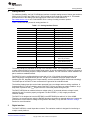
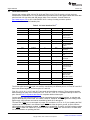
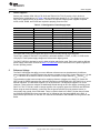
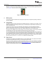
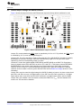
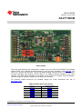
User's Guide
SBAU159 – October 2009
DAC7716EVM
DAC7716EVM
This user's guide describes the characteristics, operation, and use of the DAC7716EVM. The evaluation
module (EVM) is an evaluation board that allows for quick and easy evaluation of the DAC7716. The
DAC7716 is a quad, high-accuracy, 12-bit R-2-R digital-to-analog converter (DAC). The device features
low-power operation, good linearity, and the ability to use different reference voltages for the output
channels. This EVM allows evaluation of all aspects of the DAC7716. Complete circuit descriptions,
schematic diagrams, and bill of material are included in this document.
The following related documents are available through the Texas Instruments web site at
http://www.ti.com.
EVM-Compatible Device Data Sheets
Device
Literature Number
DAC7716
SBAS463
REF5025
SBOS410
REF5050
SBOS410
OPA211
SBOS377
TL750L08
SLVS017
All trademarks are the property of their respective owners.
SBAU159 – October 2009
Submit Documentation Feedback
DAC7716EVM
Copyright © 2009, Texas Instruments Incorporated
1
EVM Overview
1
2
3
4
5
6
7
www.ti.com
Contents
EVM Overview ...............................................................................................................
Analog Interface .............................................................................................................
Digital Interface ..............................................................................................................
Power Supplies ..............................................................................................................
Reference Voltage ..........................................................................................................
EVM Operation ..............................................................................................................
Schematics and Layout ....................................................................................................
2
3
3
5
5
6
8
List of Figures
1
Reference Test Points ...................................................................................................... 6
2
DAC7716EVM Default Jumper Locations
7
3
Default Settings for Switch S1 (LDAC Low)
8
4
...............................................................................
............................................................................
Default Settings for Switch S2 and S3 ...................................................................................
8
List of Tables
1
J1: Analog Interface Pinout ................................................................................................ 3
2
J2: Serial Interface Pins
3
4
...................................................................................................
J3 Configuration: Power-Supply Input ....................................................................................
DAC7716EVM Bill of Materials ...........................................................................................
1
EVM Overview
1.1
Features
4
5
9
DAC7716EVM:
• Contains all support circuitry needed for the DAC7716
• Voltage reference options: Either 5V or 2.5V onboard, or external
• Jumpers on output pins for gain adjustment
• Compatible with the TI Modular EVM System
This manual covers the operation of the DAC7716EVM. Throughout this document, the abbreviation EVM
and the term evaluation module are synonymous with the DAC7716EVM.
1.2
Introduction
The DAC7716 uses a high-speed SPI interface (up to 50MHz) to communicate with a DSP or a
microprocessor using a compatible serial interface. The DAC features four individual outputs whose gain
is controlled by the addition of a feedback resistor. An additional VMON pin can relay any of the four output
channels from the DAC or the signal from the AIN pin.
The DAC7716EVM is designed to run in either bipolar (default mode) or unipolar modes of operation. This
flexible design allows for a wide range of supply voltages. The operating mode can be controlled using an
onboard switch or digitally, through the digital header.
The DAC7716EVM is an evaluation module built to the TI Modular EVM System specification. It can be
connected to any modular EVM system interface card. The EVM ships in the TQFP-48 pin package
option.
Note that the DAC7716EVM has no microprocessor and cannot run software. To connect it to a computer,
some type of interface is required.
The device shown in the front-page figure is the DAC8734, the 16-bit version of the DAC7716. The
DAC7716 is installed in place of the DAC8734 on the DAC7716 evaluation module.
2
DAC7716EVM
SBAU159 – October 2009
Submit Documentation Feedback
Copyright © 2009, Texas Instruments Incorporated
Analog Interface
www.ti.com
2
Analog Interface
For maximum flexibility, the DAC7716EVM can interface to multiple analog sources. Samtec part numbers
SSW-110-22-F-D-VS-K and TSM-110-01-T-DV-P provide a 10-pin, dual-row, header at J1. This header
provides access to the analog input and output pins of the DAC. Consult Samtec at
http://www.samtec.com or call 1-800-SAMTEC-9 for a variety of mating connector options.
Table 1 summarizes the pinouts for analog interface J1.
Table 1. J1: Analog Interface Pinout
Pin Number
Signal
Description
J1.1
SGND-0
Signal GND DAC output 0
J1.2
VOUT-0
Analog output 0
J1.3
SGND-1
Signal GND DAC output 1
J1.4
VOUT-1
Analog output 1
J1.5
SGND-2
Signal GND DAC output 2
J1.6
VOUT-2
Analog output 2
J1.7
SGND-3
Signal GND DAC output 3
J1.8
VOUT-3
Analog output 3
J1.9-13 (odd)
AGND
Analog ground connections
J1.10
AIN
Auxiliary analog input
J1.14
VMON_BUF
Monitor output after buffer
J1.15
Unused
—
J1.17-19 (odd)
AGND
Analog ground connections
J1.18
RefGND
Reference ground pins on the
DAC7716 (see below)
J1.20
EXTREF+
External reference source input (+
side of reference input)
J1.12
Unused
—
J1.16
Unused
—
The analog interface is populated on the top of the evaluation model. This configuration makes it possible
to stack multiple EVMs to run them in daisy-chain mode. J4 can be installed with a 90-degree connector to
allow access to the analog outputs if multiple EVMs are stacked. The J1B connector can be installed if the
part is used as a standalone board.
The DAC7716 can be configured with an output gain of 2 or 4. By default, the analog outputs of the
DAC7716EVM are configured with a gain of 4. If a gain of 2 is desired, the proper jumper must be
installed (JP2-JP5, depending on the output channel), and the command register must be set accordingly.
The SGND pins of the DAC7716 are connected to the ground of the evaluation board.
The Auxiliary Analog Input pin can be further protected from over-voltage and over-driving conditions. A
Schottky diode (D1) can be installed to protect the DAC7716 from an input over-voltage condition. An op
amp buffer is placed on the VMON output to limit the current that passes through the pin.
The DAC7716EVM has an external reference voltage option. If an external reference voltage is used,
switches S2 and S3 must be properly configured. Use the EXTREF+ (J1.20) to apply an external
reference voltage.
The DAC7716 is designed to have the REFGND-A and REFGND-B pins within 0.3V of the AGND.
Therefore, we recommend not using the RefGND pin when connecting an external reference. Connect the
ground source of the reference voltage to the ground of the board (J1.19). See the Reference Voltage
section for more information.
3
Digital Interface
The DAC7716EVM is a serial input data converter. The evaluation module is designed for interfacing to
multiple control platforms.
SBAU159 – October 2009
Submit Documentation Feedback
DAC7716EVM
Copyright © 2009, Texas Instruments Incorporated
3
Digital Interface
3.1
www.ti.com
Serial Data Interface
Samtec part numbers SSW-110-22-F-D-VS-K and TSM-110-01-T-DV-P provide a 10-pin, dual-row,
header/socket combination at J2. This header/socket provides access to the digital control and serial data
pins from both J2A (top side) and J2B (bottom side) of the connector. Consult Samtec at
http://www.samtec.com or call 1-800-SAMTEC-9 for a variety of mating connector options.
Table 2 describes the serial interface pins.
Table 2. J2: Serial Interface Pins (1)
(1)
Pin No.
Signal Name
I/O Type
Pullup
Function
J2.1
Unused
—
—
J2.2
GPIO-0
In/Out
High
GPIO-0
J2.3 J2.5
SCLK
In
None
DAC7716 SPI
clock; pins are
shorted together
J2.4
DGND
In/Out
None
Digital ground
J2.6
GPIO-1
In/Out
High
GPIO-1
J2.7 J2.9
CS
In
None
SPI bus chip select;
pins are shorted
together
J2.8
Uni/Bip A
In
High
Output mode select
of Group A
J2.10
DGND
In/Out
None
Digital ground
J2.11
SDO/SDI
In/Out
None
DAC7716 SPI data
in/out
J2.12
Uni/Bip B
In
High
Output mode select
of Group B
J2.13
Unused
—
—
J2.14
RST
In
High
Input register reset
J2.15
LDAC
In
High
GPIO signal to
control LDAC for
DAC output latch
update
J2.16
Unused
—
—
J2.17
LDAC
In
High
Alternate GPIO
signal to control
LDAC for DAC
output latch update
J2.18
DGND
In/Out
None
Digital ground
J2.19
Unused
—
—
J2.20
Unused
—
—
Group A contains VOUT-0 and VOUT-1. Group B contains VOUT-2 and VOUT-3.
The SCLK signal and the CS signal can each be controlled by two different pins on J2. Pins J2.3 and J2.5
have been shorted together, as well as pins J2.7 and J2.9.
Pins J2.8, J2.12, J2.14, J2.15, and J2.17 have weak pull-up/pulldown resistors. These resistors provide
default settings for many of the control pins. J2.3, J2.5, J2.7, J2.9, J2.11 correspond directly to DAC7716
pins. See the DAC7716 product data sheet for complete details on these pins.
Control signals to and from the DAC7716 can be accessed through the digital interface, or switches and
jumpers found directly on the EVM. The /LDAC, Uni/Bip A, Uni/Bip B, and RST signals are initially pulled
high through 10kΩ resistors and can be controlled by switch S1 or through J2.
The load DAC (LDAC) pin is connected via jumper JP1 to either the J2.15 or J2.17 pin. Updating the DAC
registers can be completed in two different ways. LDAC can either be tied to ground, in which case the
input registers are immediately updated, or LDAC can be pulled high. Therefore, the DAC registers update
when LDAC is taken low. Switch S1.1 can be closed to hold the LDAC low. See the DAC7716 data sheet
for more information on updating the DAC.
4
DAC7716EVM
SBAU159 – October 2009
Submit Documentation Feedback
Copyright © 2009, Texas Instruments Incorporated
Power Supplies
www.ti.com
4
Power Supplies
Samtec part numbers SSW-105-22-F-D-VS-K and TSM-105-01-T-DV-P provide a 5-pin, dual-row,
header/socket combination at J3. Table 3 lists the configuration details for J3. The voltage inputs to the
DAC can be applied directly to the device. The DAC7716 requires multiple power supplies to operate.
AVDD, AVSS, DVDD, and IOVDD are required to properly power the DAC.
Table 3. J3 Configuration: Power-Supply Input
Pin No.
Pin Name
Function
Required
J3.1
+VA
+4.75V to +24V analog supply
Yes
J3.2
–VA
–18V to –4.75V analog supply
Yes
J3.3
+5VA
+5V analog supply
No
J3.4
–5VA
–5V analog supply
No
J3.5
DGND
Digital ground input
Yes
J3.6
AGND
Analog ground input
Yes
J3.7
+1.8VD
1.8V digital supply
Optional
J3.8
+3.3VD
3.3V digital supply
Optional
J3.9
VD1
Not used
No
J3.10
+5VD
+5V
Yes
The Digital and Analog ground inputs are short-circuited internally through a ground plane.
The dc logic voltage for the DAC7716 (IOVDD) is selectable between +3.3VD, +1.8VD, or +5VD via the
JP8 jumper. These power-supply voltages are referenced to digital ground.
The DAC7716EVM is designed to work in either unipolar and bipolar mode. Each mode requires different
power-supply connections. Consult the DAC7716 data sheet for the restrictions on the power supplies for
the two operating modes.
5
Reference Voltage
The DAC7716EVM has the ability to use two different reference sources simultaneously for different
output channels. REFA and REFB control the reference voltages for the DAC. Output channels VOUT-0 and
VOUT-1 use REFA as a reference. REFB is used as a reference for output channels VOUT-2 and VOUT-3.
The evaluation module has three options for supplying reference voltages to the DAC7716. Switch S3
(REFA) and S2 (REFB) can select the reference voltage from the REF5050 (U5), REF5025 (U4) or use an
external reference. The REF5050 supplies 5.0V to the reference. The REF5025 supplies 2.5V to the
reference. These reference voltages are additionally filtered through an RC filter before connecting to the
DAC7716. The TL751L08 is used to voltage regulate +VA to properly power the REF5025 and REF5050.
When using an external reference, make sure that the ground terminal (from the external source) is
connected to the ground of the EVM board. There is a built-in diode in the DAC7716 that does not allow
the RefGND-A/RefGND-B to have more than a 0.3V difference from the board AGND on the DAC. A
jumper across pins 2 and 3 on JP6 and JP7 connects the RefGND-A and RefGND-B to the ground of the
board.
SBAU159 – October 2009
Submit Documentation Feedback
DAC7716EVM
Copyright © 2009, Texas Instruments Incorporated
5
EVM Operation
www.ti.com
Note that if an external reference voltage is input to J1.20, it will be filtered through a first-order, low-pass
RC filter. To input your own reference signal without this filter, connect the reference signal directly to TP1
or TP2. Figure 1 shows the reference test points on the EVM.
Figure 1. Reference Test Points
6
EVM Operation
This section provides information on the analog input, digital control, and general operating conditions of
the DAC7716EVM.
6.1
Analog Output
The DAC7716 has four analog outputs that are available through the J1 header or the J4 header. The J4
header is designed to use 90-degree Samtec pins (not installed) when multiple EVMs are stacked to be
used in daisy-chain mode.
Jumpers J5-J8 control the gain of the individual output channels by connecting additional feedback
resistors to the internal op amp buffer. See the DAC7716 data sheet for more information on setting the
gain. Each analog output is able to swing ±16V in bipolar mode and 0 to 20V in unipolar mode.
The signal ground, SGND-N (for the output signals), are connected to header J1 and are short-circuited to
the board ground. All of the output signals are referenced to the ground of the board.
VMON is the channel monitor output. It can relay any of the four analog output signals or the AIN signal. The
VMON signal is buffered and current-limited through the OPA227 (U2). By default, the VMON pin is in 3-state
mode, causing the op amp to saturate. In order to avoid the op amp saturating to a rail, a 200kΩ resistor is
put in place. The resistor serves as a load for the op amp when the VMON pin is in 3-state mode. However,
as a result, there is an error of ~1% on the VMON_BUF signal when relaying a signal.
6.2
Digital Control
The digital control signals can be applied directly to J1 (top or bottom side). The modular DAC7716EVM
can also be connected directly to a DSP or microcontroller interface board.
No specific evaluation software is provided with this EVM; however, various code examples are available
that show how to use EVMs with a variety of digital signal processors from Texas Instruments. Check the
respective product folders or send an e-mail to [email protected] for a listing of available code
examples. The EVM Gerber files are also available on request.
6
DAC7716EVM
SBAU159 – October 2009
Submit Documentation Feedback
Copyright © 2009, Texas Instruments Incorporated
EVM Operation
www.ti.com
6.3
Default Jumper Settings and Switch Positions
Figure 2 shows the jumpers found on the EVM and the respective factory default conditions for each.
Figure 2. DAC7716EVM Default Jumper Locations
Jumper JP1 controls whether the LDAC signal is controlled by J2.15 or J2.17. By default, the LDAC signal
is controlled by J2.17 but can be changed using JP1.
Jumpers JP2, JP3, JP4, and JP5 are used to control the gain of the individual DAC channels. By default,
the jumpers are removed, resulting in each DAC channel having a gain of 4. The gain of the output
channel is 2 when the corresponding jumper is in place.
JP6 and JP7 control the signals applied to REFGND-A and REFGND-B on the DAC7716. By default, a
jumper is placed across JP6.2 and JP6.3 as well as JP7.2 and JP7.3. This jumper connects REFGND-A
and REFGND-B to the ground of the board when an onboard reference is used. When an external
reference source is used, it is recommended that this jumper stay in place and configure the external
reference source to share a common ground with the EVM. See the Reference Voltage section for more
information.
Jumper JP8 is used to control the digital voltage for IOVDD. By default, a jumper is in place to short-circuit
pins JP8.1 and JP8.2 to use a 3.3V digital supply. If pins JP8.3 and JP8.4 are connected, a 1.8V digital
supply will be used. If pins JP8.5 and JP8.6 are connected, a 5V digital supply will be used for IOVDD.
Jumper JP9 is not installed. If the user desires to disconnect RFB1 from VOUT1, the trace between JP9
must be cut. JP9 can then be installed.
SBAU159 – October 2009
Submit Documentation Feedback
DAC7716EVM
Copyright © 2009, Texas Instruments Incorporated
7
Schematics and Layout
www.ti.com
Switch S1 allows the user to pull down four control signals to ground. LDAC, Uni/Bip B, RST, and Uni/Bip
A can be pulled low using the switch. By default, switch position S1.1 is open, causing LDAC to be
connected to ground. Switches S1.2 and S1.4 are open to short-circuit Uni/Bip A and Uni/Bip B to ground.
This configuration sets the DAC7716 to bipolar mode (default). Figure 3 shows the default settings for
switch S1.
Figure 3. Default Settings for Switch S1 (LDAC Low)
Switch S2 controls the reference voltage selection for Ref B. When the switch is furthest left (position 1),
the onboard 5V reference is used from the REF5050. When the switch is in the middle position (position
2), the onboard 2.5V reference is used from the REF5025. If the switch is moved to the right (position 3),
Ref B is set up to use an external reference. Pins J1.18 (Ref–) and J1.20 (Ref+) are used to apply an
external reference voltage.
Switch S3 controls the reference voltage selection for Ref A. The switch has the same functionality as
switch S2. By default, switch S2 and switch S3 are set to use the 5V onboard reference, as Figure 4
shows.
Figure 4. Default Settings for Switch S2 and S3
7
Schematics and Layout
Schematics for the DAC7716EVM are appended to this user's guide. The bill of materials is provided in
Table 4.
7.1
Bill of Materials
NOTE: All components should be compliant with the European Union Restriction on Use of
Hazardous Substances (RoHS) Directive. Some part numbers may be either leaded or
RoHS. Verify that purchased components are RoHS-compliant. (For more information about
TI's position on RoHS compliance, see the TI web site.)
8
DAC7716EVM
SBAU159 – October 2009
Submit Documentation Feedback
Copyright © 2009, Texas Instruments Incorporated
Schematics and Layout
www.ti.com
space
Table 4. DAC7716EVM Bill of Materials (1)
(1)
(2)
Item No.
Qty
Ref Des
Description
Manufacturer
N/A
Printed wiring board
Texas Instruments
C1, C6, C10,
C11, C14, C15
Capacitor, ceramic 1.0µF 16V X5R
10% 0603
TDK
C2, C3, C4,
C5, C7, C8,
C9
Capacitor, ceramic 10µF 25V X5R
1206 10%
MuRata
C12, C13,
C16, C 17
Capacitor, ceramic 10µF 10V 0603
X5R 20%
Panasonic
Mfr Part Number
1
1
2
6
3
7
4
4
5
0
D1
Not installed
N/A
6
3
JP1, JP6, JP7
Header strip, 3-pin (1x3)
Samtec
TSW-103-07-L-S
7
5
JP2, JP3, JP4,
JP5, JP9
Header strip, 2-pin (1x2)
Samtec
TSW-102-07-L-S
8
1
JP8
Header strip, 6-pin (2x3)
Samtec
TSW-103-07-L-D
9
2
J1A, J2A
(Top Side)
10-Pin, Dual Row, SM Header (20
Pos.)
Samtec
TSM-110-01-T-DV-P
10
0
J1B
(Bottom Side)
Not installed
N/A
11
1
J2B
(Bottom Side)
10-Pin, Dual Row, SM Header (20
Pos.)
Samtec
SSW-110-22-F-D-VS-K
12
1
J3A
(Top Side)
5-Pin, Dual Row, SM Header (10 Pos.)
Samtec
TSM-105-01-T-DV-P
13
1
J3B (2)
(Bottom Side)
5-Pin, Dual Row, SM Header (10 Pos.)
Samtec
SSW-105-22-F-D-VS-K
14
0
J4
Not installed
N/A
15
5
R1, R2, R3,
R4, R5
Resistor 33 Ω 1/10W 5% 0603 SMD
Panasonic
16
6
R6, R7, R8,
R9, R10, R11
Resistor 10 kΩ 1/10W 5% 0603 SMD
Yageo
17
2
R12, R13
Resistor 1.0 kΩ 1/10W 5% 0603 SMD
Panasonic
ERJ-3GEYJ102V
18
2
R14, R15
Resistor 1.0 Ω 1/10W 5% 0603
Panasonic
ERJ-3GEYJ1R0V
19
1
R16
Resistor 200 kΩ 1/10W 1% 0603 SMD
Panasonic
ERJ-3EKF2003V
20
1
S1
Switch Dip Tape 4 pos
C&K
TDA04H0SB1R
21
2
S2, S3
SW SLIDE ULTRA MINI SP3T TOP
ACT
NKK
SS14MDP2
22
3
TP1, TP2 ,TP3
Test Point - Single .025 Pin, Red
Keystone
5000
23
2
TP4, TP5
Test Point - Single .025 Pin, Black
Keystone
5001
24
1
U1
Quad, 12-bit, High Accuracy DAC,
TQFP Package
Texas Instruments
DAC7716SPFB
25
1
U2
OPA227, Differential Operational
Amplifier
Texas Instruments
OPA227UA
26
1
U3
Single output, 8V voltage regulator
Texas Instruments
TL750L08CD
27
1
U4
Precision Voltage reference 2.5V
Texas Instruments
REF5025AID
28
1
U5
Precision Voltage reference 5.0V
Texas Instruments
REF5050AID
29
8
N/A
0.100 Shunt - Black
Samtec
6508538
C1608X5R1C105K
GRM31CR61E106KA12L
ECJ-1VB1A106M
N/A
N/A
N/A
ERJ-3GEYJ330V
RC0603JR-0710KL
SNT-100-BK-T
Manufacturer and part number for items may be substituted with electrically equivalent items.
J3B parts are not shown in the schematic diagram. J3B is installed on the bottom side of the PWB opposite to J3A.
SBAU159 – October 2009
Submit Documentation Feedback
DAC7716EVM
Copyright © 2009, Texas Instruments Incorporated
9
1
2
3
4
6
5
REVISION HISTORY
REV
IOVDD
+VA
-VA
ENGINEERING CHANGE NUMBER
APPROVED
+5VD
LDAC
SDO
C3
10uF
C1
1uF
CS
C4
10uF
C6
1uF
C2
10uF
C5
10uF
SCLK
D
Uni/Bip A
Uni/Bip B
RST
10
48
36
37
1
25
24
19
12
42
GPIO-0
8
7
6
5
GPIO-1
GPIO-1
Uni/Bip A
S1
DIPSWITCH-4
Uni/Bip B
RST
29
30
14
28
33
K1 A1
D1A
REFGND-A
NC
NC
NC
NC
NC
NC
NC
NC
200k
7
-VA
J1A
10uF
23
21
22
20
JP9
46
44
45
43
Vout-2
RFB1-2
RFB2-2
SGND-2
1
3
5
7
9
11
13
15
17
19
JP2
2
4
6
8
10
12
14
16
18
20
A0(+)
A1(+)
A2(+)
A3(+)
A4
A5
A6
A7
REFREF+
Vout-0
Vout-1
Vout-2
Vout-3
Vmon_buf
J4
8
7
6
5
4
3
2
1
Ain
ExtREFExtREF+
HEADER-8
C
JP4
J1B
1
3
5
7
9
11
13
15
17
19
JP5
32
31
8
9
11
SDI
27
TP3
A0(-)
A1(-)
A2(-)
A3(-)
AGND
AGND
AGND
VCOM
AGND
AGND
DAUGHTER-ANALOG
Analog to only be populated at top of board
JP3
38
40
39
41
Vout-3
RFB1-3
RFB2-3
SGND-3
RST
R16
4
REF-A
DVDD
AVSS
AVSS
U1
DAC7716
C8
1
Serial Header Bottom
J2B
34
15
17
16
18
Vout-1
RFB1-1
RFB2-1
SGND-1
3
7
6
Ain
Uni/Bip A
Uni/Bip B
10uF
OPA227
3
Vout-0
RFB1-0
RFB2-0
SGND-0
REF-B
GPIO-0
2
4
6
8
10
12
14
16
18
20
1
2
3
4
1
3
5
7
9
11
13
15
17
19
C
2
Vmon
GPIO-0
GPIO-1
3POS_JUMPER
CS
SCLK
SDI
SDO
LDAC
U2
REFGND-B
2
3
4
5
6
33
33
33
33
33
47
JP1
AVDD
AVDD
IOVDD
D1B
AGND
R1
R2
R3
R4
R5
CS
SCLK
SDI
SDO
LDAC
Serial Header Top
J2A
C7
+VA
K2 A2
Uni/Bip B
RST
R9 R10 R11
10k 10k 10k
DGND
R6 R7 R8
10k 10k 10k
26
35
13
GPIO-1
Uni/Bip A
2
2
4
6
8
10
12
14
16
18
20
3
1
3
5
7
9
11
13
15
17
19
D
GPIO-0
2
4
6
8
10
12
14
16
18
20
DAUGHTER ANALOG BOTTOM
-VA
CS
SCLK
JP6 and JP7 control the RefGND
JP7
3POS_JUMPER
+VA
TP1
B
3
2
1
U3
TL750L08
C9
10uF
5
Com
NC
Com
NC
Com
C
R12
1k
B
JP6
3POS_JUMPER
NKK_SS14MDP2
S2
1
2
C10
1uF
3
2
3
4
VIN
VOUT
TEMP
GND TRIM
6
TP5
5
R14
1
REF5050
6
TP4
C16
10uF
U5
ExtREF+
C14
1uF
7
4
Output
Input
Com
8
3
2C
1
C12
10uF
+3.3VD +1.8VD +5VA
+VA
-VA
-5VA
+5VD
J3
1
3
5
7
9
U4
C11
1uF
2
3
4
VIN
VOUT
TEMP
GND TRIM
6
5
TP2
R15
1
REF5025
C15
1uF
2
4
6
8
10
ti
DAUGHTER-POWER
R13
1k
C13
10uF
S3
NKK_SS14MDP2
C17
10uF
PRECISION ANALOG PRODUCTS
HIGH-PERFORMANCE ANALOG DIVISION
SEMICONDUCTOR GROUP
2
4
6
A
+VA
-VA
+5VA
-5VA
DGND AGND
+1.8VD
VD1
+3.3VD +5VD
5411 EAST WILLIAMS BOULEVARD, TUCSON, AZ 85711 USA
JP8
JPR-2X3
1
3
5
IOVDD
ENGINEER T.
Calabria
DRAWN BYT.
Calabria
TITLE
DOCUMENT CONTROL NO.6508538 SIZE B
SHEET
1
2
3
4
5
OF
DAC8734EVM
DATE
REV
FILE
6
A
A
Evaluation Board/Kit Important Notice
Texas Instruments (TI) provides the enclosed product(s) under the following conditions:
This evaluation board/kit is intended for use for ENGINEERING DEVELOPMENT, DEMONSTRATION, OR EVALUATION
PURPOSES ONLY and is not considered by TI to be a finished end-product fit for general consumer use. Persons handling the
product(s) must have electronics training and observe good engineering practice standards. As such, the goods being provided are
not intended to be complete in terms of required design-, marketing-, and/or manufacturing-related protective considerations,
including product safety and environmental measures typically found in end products that incorporate such semiconductor
components or circuit boards. This evaluation board/kit does not fall within the scope of the European Union directives regarding
electromagnetic compatibility, restricted substances (RoHS), recycling (WEEE), FCC, CE or UL, and therefore may not meet the
technical requirements of these directives or other related directives.
Should this evaluation board/kit not meet the specifications indicated in the User’s Guide, the board/kit may be returned within 30
days from the date of delivery for a full refund. THE FOREGOING WARRANTY IS THE EXCLUSIVE WARRANTY MADE BY
SELLER TO BUYER AND IS IN LIEU OF ALL OTHER WARRANTIES, EXPRESSED, IMPLIED, OR STATUTORY, INCLUDING
ANY WARRANTY OF MERCHANTABILITY OR FITNESS FOR ANY PARTICULAR PURPOSE.
The user assumes all responsibility and liability for proper and safe handling of the goods. Further, the user indemnifies TI from all
claims arising from the handling or use of the goods. Due to the open construction of the product, it is the user’s responsibility to
take any and all appropriate precautions with regard to electrostatic discharge.
EXCEPT TO THE EXTENT OF THE INDEMNITY SET FORTH ABOVE, NEITHER PARTY SHALL BE LIABLE TO THE OTHER
FOR ANY INDIRECT, SPECIAL, INCIDENTAL, OR CONSEQUENTIAL DAMAGES.
TI currently deals with a variety of customers for products, and therefore our arrangement with the user is not exclusive.
TI assumes no liability for applications assistance, customer product design, software performance, or infringement of
patents or services described herein.
Please read the User’s Guide and, specifically, the Warnings and Restrictions notice in the User’s Guide prior to handling the
product. This notice contains important safety information about temperatures and voltages. For additional information on TI’s
environmental and/or safety programs, please contact the TI application engineer or visit www.ti.com/esh.
No license is granted under any patent right or other intellectual property right of TI covering or relating to any machine, process, or
combination in which such TI products or services might be or are used.
FCC Warning
This evaluation board/kit is intended for use for ENGINEERING DEVELOPMENT, DEMONSTRATION, OR EVALUATION
PURPOSES ONLY and is not considered by TI to be a finished end-product fit for general consumer use. It generates, uses, and
can radiate radio frequency energy and has not been tested for compliance with the limits of computing devices pursuant to part 15
of FCC rules, which are designed to provide reasonable protection against radio frequency interference. Operation of this
equipment in other environments may cause interference with radio communications, in which case the user at his own expense
will be required to take whatever measures may be required to correct this interference.
EVM Warnings and Restrictions
It is important to operate this EVM within the input voltage range of –16.5V to +21V and the output voltage range of –15V to +15V.
Exceeding the specified input range may cause unexpected operation and/or irreversible damage to the EVM. If there are
questions concerning the input range, please contact a TI field representative prior to connecting the input power.
Applying loads outside of the specified output range may result in unintended operation and/or possible permanent damage to the
EVM. Please consult the EVM User's Guide prior to connecting any load to the EVM output. If there is uncertainty as to the load
specification, please contact a TI field representative.
During normal operation, some circuit components may have case temperatures greater than +30° C. The EVM is designed to
operate properly with certain components above +60° C as long as the input and output ranges are maintained. These components
include but are not limited to linear regulators, switching transistors, pass transistors, and current sense resistors. These types of
devices can be identified using the EVM schematic located in the EVM User's Guide. When placing measurement probes near
these devices during operation, please be aware that these devices may be very warm to the touch.
Mailing Address: Texas Instruments, Post Office Box 655303, Dallas, Texas 75265
Copyright © 2009, Texas Instruments Incorporated
IMPORTANT NOTICE
Texas Instruments Incorporated and its subsidiaries (TI) reserve the right to make corrections, modifications, enhancements, improvements,
and other changes to its products and services at any time and to discontinue any product or service without notice. Customers should
obtain the latest relevant information before placing orders and should verify that such information is current and complete. All products are
sold subject to TI’s terms and conditions of sale supplied at the time of order acknowledgment.
TI warrants performance of its hardware products to the specifications applicable at the time of sale in accordance with TI’s standard
warranty. Testing and other quality control techniques are used to the extent TI deems necessary to support this warranty. Except where
mandated by government requirements, testing of all parameters of each product is not necessarily performed.
TI assumes no liability for applications assistance or customer product design. Customers are responsible for their products and
applications using TI components. To minimize the risks associated with customer products and applications, customers should provide
adequate design and operating safeguards.
TI does not warrant or represent that any license, either express or implied, is granted under any TI patent right, copyright, mask work right,
or other TI intellectual property right relating to any combination, machine, or process in which TI products or services are used. Information
published by TI regarding third-party products or services does not constitute a license from TI to use such products or services or a
warranty or endorsement thereof. Use of such information may require a license from a third party under the patents or other intellectual
property of the third party, or a license from TI under the patents or other intellectual property of TI.
Reproduction of TI information in TI data books or data sheets is permissible only if reproduction is without alteration and is accompanied
by all associated warranties, conditions, limitations, and notices. Reproduction of this information with alteration is an unfair and deceptive
business practice. TI is not responsible or liable for such altered documentation. Information of third parties may be subject to additional
restrictions.
Resale of TI products or services with statements different from or beyond the parameters stated by TI for that product or service voids all
express and any implied warranties for the associated TI product or service and is an unfair and deceptive business practice. TI is not
responsible or liable for any such statements.
TI products are not authorized for use in safety-critical applications (such as life support) where a failure of the TI product would reasonably
be expected to cause severe personal injury or death, unless officers of the parties have executed an agreement specifically governing
such use. Buyers represent that they have all necessary expertise in the safety and regulatory ramifications of their applications, and
acknowledge and agree that they are solely responsible for all legal, regulatory and safety-related requirements concerning their products
and any use of TI products in such safety-critical applications, notwithstanding any applications-related information or support that may be
provided by TI. Further, Buyers must fully indemnify TI and its representatives against any damages arising out of the use of TI products in
such safety-critical applications.
TI products are neither designed nor intended for use in military/aerospace applications or environments unless the TI products are
specifically designated by TI as military-grade or "enhanced plastic." Only products designated by TI as military-grade meet military
specifications. Buyers acknowledge and agree that any such use of TI products which TI has not designated as military-grade is solely at
the Buyer's risk, and that they are solely responsible for compliance with all legal and regulatory requirements in connection with such use.
TI products are neither designed nor intended for use in automotive applications or environments unless the specific TI products are
designated by TI as compliant with ISO/TS 16949 requirements. Buyers acknowledge and agree that, if they use any non-designated
products in automotive applications, TI will not be responsible for any failure to meet such requirements.
Following are URLs where you can obtain information on other Texas Instruments products and application solutions:
Products
Amplifiers
Data Converters
DLP® Products
DSP
Clocks and Timers
Interface
Logic
Power Mgmt
Microcontrollers
RFID
RF/IF and ZigBee® Solutions
amplifier.ti.com
dataconverter.ti.com
www.dlp.com
dsp.ti.com
www.ti.com/clocks
interface.ti.com
logic.ti.com
power.ti.com
microcontroller.ti.com
www.ti-rfid.com
www.ti.com/lprf
Applications
Audio
Automotive
Broadband
Digital Control
Medical
Military
Optical Networking
Security
Telephony
Video & Imaging
Wireless
www.ti.com/audio
www.ti.com/automotive
www.ti.com/broadband
www.ti.com/digitalcontrol
www.ti.com/medical
www.ti.com/military
www.ti.com/opticalnetwork
www.ti.com/security
www.ti.com/telephony
www.ti.com/video
www.ti.com/wireless
Mailing Address: Texas Instruments, Post Office Box 655303, Dallas, Texas 75265
Copyright © 2009, Texas Instruments Incorporated