1
Hardware Description
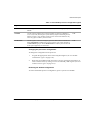
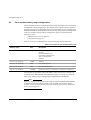
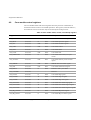
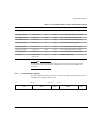
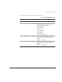
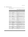
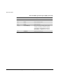
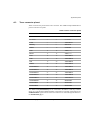
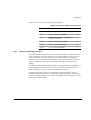
Table 3-6 JTAG signal description (continued)
Name
Description
Function
nSRST
System reset (bidirectional)
nSRST is an active LOW open-collector signal which can be
driven by the JTAG equipment to reset the target board. Some
JTAG equipment senses this line to determine when a board has
been reset by the user.
The open collector nSRST reset signal can be driven LOW by the
reset controller on the core module to cause the motherboard to
reset the whole system by driving nSYSRST LOW.
This is also used in configuration mode to control the initialization
pin (nINIT) on the FPGAs.
Though not a JTAG signal, nSRST is described because it can be
controlled by JTAG equipment.
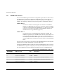
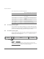
nTRST
Test reset (from JTAG
equipment)
This active LOW open-collector signal is used to reset the JTAG
port and the associated debug circuitry on the processor. It is
asserted at power-up by each module, and can be driven by the
JTAG equipment. This signal is also used in configuration mode
to control the programming pin (nPROG) on FPGAs.
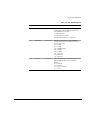
RTCK
Return TCK
(to JTAG equipment)
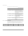
Some devices sample TCK (for example a synthesizable core with
only one clock), and this has the effect of delaying the time at
which a component actually captures data. RTCK is a mechanism
for returning the sampled clock to the JTAG equipment, so that the
clock is not advanced until the synchronizing device captured the
data. In adaptive clocking mode, Multi-ICE is required to detect an
edge on RTCK before changing TCK. In a multiple device JTAG
chain, the RTCK output from a component connects to the TCK
input of the down-stream device. The RTCK signal on the module
connectors HDRB returns TCK to the JTAG equipment. If there
are no synchronizing components in the scan chain then it is
unnecessary to use the RTCK signal and it is connected to ground
on the motherboard.
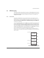
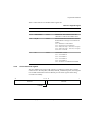
TCK
Test clock
(from JTAG equipment)
TCK synchronizes all JTAG transactions. TCK connects to all
JTAG components in the scan chain. Series termination resistors
are used to reduce reflections and maintain good signal integrity.
TCK flows down the stack of modules and connects to each JTAG
component. However, if there is a device in the scan chain that
synchronizes TCK to some other clock, then all down-stream
devices are connected to the RTCK signal on that component (see
RTCK).
3-30
Copyright © 2000 ARM Limited. All rights reserved.
ARM DUI 0138A