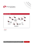
1
FEUL6636B-05 1 MSM6636/6636B User’s Manual SAE-J1850 Communication Protocol Conformed Transmission Controller for Automotive LAN Oki Electric Industry Co., Ltd. 5th EDITION ISSUE DATE: August 2001 NOTICE 1. The information contained herein can change without notice owing to product and/or technical improvements. Before using the product, please make sure that the information being referred to is up-to-date. 2. The outline of action and examples for application circuits described herein have been chosen as an explanation for the standard action and performance of the product. When planning to use the product, please ensure that the external conditions are reflected in the actual circuit, assembly, and program designs. 3. When designing your product, please use our product below the specified maximum ratings and within the specified operating ranges including, but not limited to, operating voltage, power dissipation, and operating temperature. 4. Oki assumes no responsibility or liability whatsoever for any failure or unusual or unexpected operation resulting from misuse, neglect, improper installation, repair, alteration or accident, improper handling, or unusual physical or electrical stress including, but not limited to, exposure to parameters beyond the specified maximum ratings or operation outside the specified operating range. 5. Neither indemnity against nor license of a third party’s industrial and intellectual property right, etc. is granted by us in connection with the use of the product and/or the information and drawings contained herein. No responsibility is assumed by us for any infringement of a third party’s right which may result from the use thereof. 6. The products listed in this document are intended for use in general electronics equipment for commercial applications (e.g., office automation, communication equipment, measurement equipment, consumer electronics, etc.). These products are not authorized for use in any system or application that requires special or enhanced quality and reliability characteristics nor in any system or application where the failure of such system or application may result in the loss or damage of property, or death or injury to humans. Such applications include, but are not limited to, traffic and automotive equipment, safety devices, aerospace equipment, nuclear power control, medical equipment, and life-support systems. 7. Certain products in this document may need government approval before they can be exported to particular countries. The purchaser assumes the responsibility of determining the legality of export of these products and will take appropriate and necessary steps at their own expense for these. 8. No part of the contents contained herein may be reprinted or reproduced without our prior permission. Copyright 2001 Oki Electric Industry Co., Ltd. MSM6636/6636B User’s Manual Contents Contents 1. OVERVIEW 1.1 1.2 1.3 1.4 1.5 1-1 Overview..................................................................................................................................................... 1-1 Features....................................................................................................................................................... 1-1 Pin Configuration........................................................................................................................................ 1-2 Pin Description ........................................................................................................................................... 1-3 Block Diagram............................................................................................................................................ 1-4 2. COMMUNICATION FORMATS 2.1 2.2 2-1 Frame Format.............................................................................................................................................. 2-1 PWM Bit Format ........................................................................................................................................ 2-4 3. INTERNAL REGISTER DETAILS 3.1 3.2 3.3 3.4 3.5 3.6 3.7 3.8 3.9 3.10 3.11 3.12 3.13 3.14 3-1 Transmit Register........................................................................................................................................ 3-1 Response Register....................................................................................................................................... 3-2 Transmit Status Register ............................................................................................................................. 3-2 Receive Register ......................................................................................................................................... 3-3 Receive Data Length Register..................................................................................................................... 3-5 Initialization/Read Completion Indication Register.................................................................................... 3-5 Interrupt Request Flag................................................................................................................................. 3-5 Interrupt Enable Flag (IE)........................................................................................................................... 3-7 Sleep Command Register............................................................................................................................ 3-7 Break Command Register ........................................................................................................................... 3-8 Mode Setting Register................................................................................................................................. 3-9 Physical Address Register......................................................................................................................... 3-10 Functional Address Register ..................................................................................................................... 3-10 NAK Register ........................................................................................................................................... 3-11 4. CPU INTERFACES 4-1 4.1 MSM6636 ................................................................................................................................................... 4-1 4.1.1 Clock Synchronous Serial Interface ...................................................................................................... 4-2 4.1.2 UART Interface (Start-Stop Synchronization System) ......................................................................... 4-5 4.2 MSM6636B ................................................................................................................................................ 4-8 4.2.1 Parallel Interface ................................................................................................................................... 4-8 5. FUNCTION DETAILS 5.1 5.2 5.3 5.4 5.5 5.6 5.7 5.8 5.9 5.10 5-1 Arbitration Function ................................................................................................................................... 5-1 Address Filter Function............................................................................................................................... 5-1 Automatic Retransmission Function........................................................................................................... 5-2 CPU Interrupt Function............................................................................................................................... 5-3 Receive Message Length Error Detection Function ................................................................................... 5-3 Local-Station Bus Driver Abnormal Detection Function............................................................................ 5-3 Communication Check Function between Specific Nodes ........................................................................ 5-3 Communication Check Function between Multiple Nodes ........................................................................ 5-4 Break Function............................................................................................................................................ 5-4 Fault Tolerant Function............................................................................................................................... 5-5 Contents – 1 MSM6636/6636B User’s Manual Contents 6. APPLICATION EXAMPLE 6.1 6.2 6-1 Host CPU and J1850 Line Connection Example ........................................................................................ 6-1 Initialization Routine Example .................................................................................................................. 6-3 7. ELECTRICAL CHARACTERISTICS 7-1 7.1 Absolute Maximum Ratings ....................................................................................................................... 7-1 7.2 Operation Range ......................................................................................................................................... 7-3 7.3 DC Characteristics ...................................................................................................................................... 7-3 7.4 AC Characteristics ..................................................................................................................................... 7-5 7.4.1 PWM Bit Timing................................................................................................................................... 7-5 7.4.2 CPU Interface Timing ........................................................................................................................... 7-6 7.4.3 Wakeup Input Signal........................................................................................................................... 7-11 7.4.4 Fault Tolerant Function Operation Conditions.................................................................................... 7-12 7.4.5 Reset Input Pulse Width...................................................................................................................... 7-13 8. BUS MONITOR FUNCTION 8-1 9. PACKAGE OUTLINES AND DIMENSIONS 9-1 Contents – 2 Chapter 1 OVERVIEW MSM6636/6636B User’s Manual Overview 1. OVERVIEW 1.1 Overview The MSM6636/6636B are transmission controllers for automotive LAN that conform to data communication protocol SAE-J1850. These LSI devices can realize a data bus topology bus LAN system that employs the PWM bit encoding method (41.6 kbps). In addition to a protocol control circuit, the MSM6636/6636B have an oscillation circuit, host CPU interface*, a transmit/receive buffer, and a bus receiver circuit, thereby decreasing the load on the host CPU. * MSM6636: The host CPU is accessed through clock synchronous serial/UART. MSM6636B: The host CPU is accessed through parallel interface. 1.2 Features • • • • • • • • • • • • • Conforms to SAE-J1850 CLASS B DATA COMMUNICATION NETWORK INTERFACE (issued August 12, 1991) CSMA/CD (carrier-sense multiple access with collision detection) Internal transmit buffer (1 frame) and receive buffer (2 frames) Bit encoding: PWM (pulse width modulation) Transmission speed: 41.6 kbps Multiaddress setting: 1 type of physical addressing and 15 types of functional addressing Address filter function by multiaddressing (broadcasting possible) Automatic retransmission when lost in contention or in the case of non-ACK Supports 3 types of in-frame responses 1) Single-byte response from a single recipient 2) Multibyte response from a single recipient (with CRC code) 3) Single-byte response from multiple recipients (ID response as ACK) Error detection by cyclic redundancy check (CRC) Various communication error detections Dual-wire bus abnormality detection by internal bus receiver and fault tolerant function Host CPU interface (1) MSM6636 Host CPU interface is accessed through serial interface with LSB first. Serial 4 modes supported: ① Clock synchronous serial (no parity) 1) Normal mode: 8-bit data 2) MPC mode: 8-bit data + MPC bit (address/data select bit: 1 indicates address. 0 indicates data) ② UART (parity yes/no selectable) 1) Normal mode: 1 start bit + 8-bit data + (parity) + 1 stop bit 2) MPC mode: 1 start bit + 8-bit data + MPC bit + (parity) + 1 stop bit (2) MSM6636B Host CPU interface is accessed through parallel interface. • • Sleep function Low power mode with oscillator stopped (IDS Max < 50 µA) SLEEP/WAKE-UP control from host CPU; WAKE-UP via LAN bus Package: (1) MSM6636 18-pin plastic DIP (DIP18-P-300-2.54) 18-pin plastic QFJ (QFJ18-P-R290-1.27) 24-pin plastic SOP (SOP24-P-430-1.27-K) (Product name: MSM6636RS) (Product name: MSM6636JS) (Product name: MSM6636GS-K) (2) MSM6636B 24-pin plastic SOP (SOP24-P-430-1.27-K) (Product name: MSM6636BGS-K) 30-pin plastic SSOP (SSOP30-P-56-0.65-K) (Product name: MSM6636BGS-AK) 1–1 MSM6636/6636B User’s Manual Overview 1.3 Pin Configuration (1) MSM6636 18-Pin Plastic QFJ 24-Pin Plastic SOP BO– AVDD DVDD RES 18-Pin Plastic DIP AVDD 1 18 DVDD BO– 2 17 RES BI– 3 16 INT BI– 3 16 INT BI+ 4 15 TXD BI+ 4 15 TXD BO+ 5 14 RXD BO+ 5 14 RXD 13 SCLK AGND 6 U-C 7 /PAE 12 A-D M-N 8 11 OSC0 U-C 10 OSC1 DGND 9 1 18 17 13 SCLK /PAE 7 12 A-D 8 9 10 11 M-N DGND OSC1 OSC0 AGND 6 2 AVDD 1 BO– 2 BI– 3 BI+ 4 BO+ 5 NC 6 NC 7 NC 8 AGND 9 U-C 10 M-N 11 DGND12 24 DVDD 23 RES 22 INT 21 TXD 20 RXD 19 NC 18 NC 17 NC 16 SCLK/PAE 15 A-D 14 OSC0 13 OSC1 NC: No Connection (2) MSM6636B 30-Pin Plastic SSOP 24-Pin Plastic SOP WR 1 RD 2 ALE 3 INT 4 RES 5 AVDD 6 BO– 7 BI– 8 BI+ 9 BO+ 10 AGND 11 DGND 12 DVDD AD7 22 AD6 21 AD5 20 AD4 19 AD3 18 AD2 17 AD1 16 AD0 15 CS 14 OSC0 13 OSC1 24 23 WR 1 RD 2 NC 3 ALE 4 INT 5 RES 6 AVDD 7 NC 8 BO– 9 BI– 10 BI+ 11 BO+ 12 NC 13 AGND 14 DGND 15 DVDD AD7 28 NC 27 AD6 26 AD5 25 AD4 24 AD3 23 NC 22 AD2 21 AD1 20 AD0 19 CS 18 NC 17 OSC0 16 OSC1 30 29 NC: No Connection Refer to Chapter 9 for package dimension information. 1–2 MSM6636/6636B User’s Manual Overview 1.4 Pin Description (1) MSM6636 Pin Name Pin No I/O Function DIP/QFJ SOP AVDD 1 1 — Analog power supply pin BO– 2 2 O LAN BUS output– BI– 3 3 I LAN BUS input– BI+ 4 4 I LAN BUS input+ BO+ 5 5 O LAN BUS output+ AGND 6 9 — U-C 7 10 I UART (:0)/clock synchronous serial (:1) select pin Analog ground pin M-N 8 11 I MPC mode (:0)/normal mode (:1) select pin DGND 9 12 — Digital ground pin OSC1 10 13 O Crystal (or ceramic resonator) oscillation output OSC0 11 14 I A-D 12 15 I Crystal (or ceramic resonator) oscillation input 0: data communication 1: address communication SCLK/PAE 13 16 I Serial clock input/parity select pin RXD 14 20 I Serial data input pin TXD 15 21 O Serial data output pin INT 16 22 O Interrupt output pin RES 17 23 I Reset input pin DVDD 18 24 — Digital power supply pin (2) MSM6636B Pin Name Pin No I/O Function SOP SSOP WR 1 1 I Data write enable input pin RD 2 2 I Data read enable input pin ALE 3 4 I Address Latch enable input pin INT 4 5 O Interrupt output pin RES 5 6 I AVDD 6 7 — Reset input pin Analog power supply pin BO– 7 9 O LAN BUS output– BI– 8 10 I LAN BUS input– BI+ 9 11 I LAN BUS input+ BO+ 10 12 O LAN BUS output+ AGND 11 14 — Analog ground pin DGND 12 15 — Digital ground pin OSC1 13 16 O Crystal (or ceramic resonator) oscillation output OSC0 14 I Crystal (or ceramic resonator) oscillation input CS 15 17 19 I Chip select input pin AD0-7 16-23 20 to 22, 24 to 27, 29 DVDD 24 30 I/O Address input/data output pins — Digital power supply pin 1–3 MSM6636/6636B User’s Manual Overview 1.5 Block Diagram (1) MSM6636 Buffer Register CPU Serial Interface Receive Register Receive Buffer Address Register LAN Controller S-P Converter PWM Decoder CRC Checker Receive Controller Transmission Controller Transmission Register Crystal CRC Generator P-S Converter Clock Generator Bus Receiver Address Filter Status Register Response Register Degital Filter LAN Bus Input PWM Encoder LAN Bus Output MSM6636 (2) MSM6636B Buffer Register CPU Parallel Interface Receive Register Receive Buffer Address Register LAN Controller S-P Converter PWM Decoder CRC Checker Receive Controller Transmission Controller Transmission Register Crystal Clock Generator Bus Receiver Address Filter Status Register Response Register Digital Filter LAN Bus Input CRC Generator P-S Converter MSM6636B 1–4 PWM Encoder LAN Bus Output Chapter 2 COMMUNICATION FORMATS MSM6636/6636B User’s Manual Communication Formats 2. COMMUNICATION FORMATS 2.1 Frame Format 101 bits maximum SOF (A) (B) (C) (D) 3-byte header CRC EOD (E) Data Response Number of Bytes * IFS Start Of Frame Cyclic Redundancy Check End Of Data End Of Frame Inter-Frame Separation SOF: CRC: EOD: EOF: IFS: (A) EOF 1 Contents Priority and message type (B) 1 Physical address or functional address of receiver node (C) 1 Physical address of transmitter node (D) (*) Data (E) (*) In-frame response (IFR) The total sum of byte count of (D) + (E) is 0 to 8. (A) Bit Configuration of Priority and Message Type MSB LSB 7 6 5 4 3 2 1 0 H(P3) P2 P1 P0 K Y Z1 Z0 H: 0 = 3-byte header (MSM6636/6636B) 1 = 1-byte header (not applicable) (See Note below) P2 to P0: Priority setting bits Determines priority of message. The smaller the priority value, the higher the priority. Note: P2 P1 P0 0 0 0 0 0 1 1 1 1 1 0 1 Priority High Low The 1-byte header mode is not selected even if “1” is set to “H” bit. The 3-byte header mode is always selected. In the MSM6636/6636B, the “H” bit is not used for selective control of the number of header bytes. However, since “0” has priority over “1”, the priority control depends on the bit value in the “H” bit, that is, the “H” bit can be used as “P3” priority setting bit. 2–1 MSM6636/6636B User’s Manual Communication Formats Y: Address type setting bit 0 = Functional address is specified to address field (B) of receiver node. 1 = Physical address is specified to address field (B) of receiver node. K, Z1, Z0: Sets response type The response type is set by a combination of K, Z1 and Z0 bits. Message type and response type are determined by the lower 4-bits of the header byte (A), including the Y bit. Classification is shown below. The MSM6636/6636B identify each message type and makes an automatic response. ZZ KY10 Addressing IFR Type Message Type 0 0000 Functional 2 Multiple IDs received from multiple responders 1 0001 Functional 1 Broadcast *1 2 0010 Functional 2 Multiple IDs received from multiple responders 3 0011 Functional 3 Data received from selected responders 4 0100 Physical 1 ID received from selected responders 5 0101 Physical 3 Data received from selected responders 6 0110 Physical 0 SAE reserve *2 7 0111 Physical 3 Data received from selected responders 8 1000 Functional 0 To multiple responders (command/status) 9 1001 Functional 0 To multiple responders (request) A 1010 Functional 0 B 1011 Functional 0 C 1100 Physical 0 D 1101 Physical 0 E 1110 Physical 0 F 1111 Physical 0 *1 *2 Broadcast: The same data is transmitted to multiple responders selected by functional addressing. Only the responder having an ID (physical address) with the highest priority can send an ID as IFR. (IFR is sent only once, and other responder IFRs are stopped.) SAE Reserve: The MSM6636/6636B do not respond even if IFR is requested by this header, because the response type is not defined. 2–2 MSM6636/6636B User’s Manual Communication Formats [IFR Type 0] SOF Header DATA CRC EOF Frame format when an in-frame response is not requested. [IFR Type 1] SOF Header DATA CRC EOD ID EOF Responder sends ID as an in-frame response. ID is 1 byte only. Therefore, the number of bytes for sending data is a maximum of 7 bytes. [IFR Type 2] SOF Header DATA CRC EOD ID1 … IDn EOF Multiple responders send ID sequentially as in-frame responses. IDs are sent in sequence from the responder with the highest priority ID. [IFR Type 3] SOF Header DATA CRC EOD IFR DATA CRC EOF One selected responder returns multi-byte data with CRC as IFR. (B) Physical address or functional address of receive node The Y bit at the 1st byte (A) of 3-byte header determines whether an address is physical or functional. The 2nd type (B) indicates the target address. (C) Physical address of transmit node Indicates the physical address (ID) of transmit node. (D) Data 0 to 8 bytes of arbitrary data to transmit is written. Data can be increased/decreased in byte units. The maximum number of bytes is 8, including response. (E) In-frame response (IFR) Determined by the bit configuration of message type at the 1st byte (A) of header. See the classification table of IFR types. 2–3 MSM6636/6636B User’s Manual Communication Formats 2.2 PWM Bit Format ♦ Pulse Width Modulation at 41.6 kbps (Typ.) TP1 TP2 Dominant “1” Passive TP3 Dominant “0” Passive TP4 Dominant “SOF” Passive Dominant TP5 TP1 “EOD” Passive Dominant “EOF” Passive Dominant TP1 “IFS” Passive TP6 Dominant “BRK” Passive 2–4 TP1 = 24 µs TP2 = 7 µs TP3 = 15 µs TP4 = 31 µs TP5 = 48 µs TP6 = 39 µs Chapter 3 INTERNAL REGISTER DETAILS MSM6636/6636B User’s Manual Internal Register Details 3. INTERNAL REGISTER DETAILS Internal Address R/W 00H-0AH W Contents Status at Reset Transmit register Undefined Undefined 0BH-12H W Response register 13H-14H W Transmit status register 15H-1FH R Receive register 20H R Receive data length register 21H W Initialization/read completion indication register 22H-24H R/W Interrupt request flag 25H-27H R/W Interrupt enable flag 00H 28H W Sleep command register 00H Break command register 00H Undefined 00H — 00H 29H W 2AH R/W Mode setting register Undefined 00H 2BH R/W Physical address register Undefined 2CH-3AH R/W Functional address register Undefined 3BH R/W NAK register Undefined 3.1 Transmit Register MSB 00 ♦ H LSB P2 P1 P0 K Y Z1 ♦ RA7 LSB RA6 RA5 RA4 RA3 RA2 RA1 RA0 ... Receive Address Write physical address or functional address of receive node. MSB 03 ... Communication Type Write priority and type of the message. MSB 01 Z0 D7 LSB D6 D5 D4 D3 D2 D1 D0 Transmit Data 8 bytes 0A ♦ ♦ D7 D6 D5 D4 D3 D2 D1 D0 Write arbitrary data for transmitting. Address 02H is empty, which permits the write operation. The maximum number of bytes of transmit data that can be set depends upon the IFR type. 3–1 MSM6636/6636B User’s Manual Internal Register Details 3.2 Response Register MSB 0B D7 LSB D6 D5 D4 D3 D2 D1 D0 IFR type 3 Response Data 8 bytes 12 ♦ D7 D6 D5 D4 D3 D2 D1 D0 Write arbitrary data for transmitting IFR. (Only applicable for IFR type 3 transmission) 3.3 Transmit Status Register MSB 13 ♦ — LSB — — — DL3 DL2 DL1 ♦ ... Data Length Write the total number of bytes of 3-byte header and data (excluding CRC). Data written to this register becomes the transmit start command. MSB 14 DL0 — LSB — — — RL3 RL2 RL1 RL0 ... Response Data Length Write the number of bytes of data that has been written to the response register used for IFR transmission. Data written to this register becomes the response transmit standby command. This standby state continues till the response request of IFR type 3 is received and is released after transmitting the response. 3–2 MSM6636/6636B User’s Manual Internal Register Details 3.4 Receive Register Receive register configuration BUS(+) BUS(–) Receive Circuit Receive Buffer Message normal receive (RCV) Response normal receive (RSP) Receive Register Read request Internal Bus Line One frame of messages is stored in the receive register and one frame of messages in the receive buffer. Transfer from the receive buffer to the receive register is implemented at the message/response receive time. Transfer to the receive register is not implemented if communication errors or overrun errors occur when receive operation is in progress. Note: If the bus monitor mode is set to prepare a monitor tool, a transfer to the receive register is performed even when errors described above occur. (See Section 8, “Bus Monitor Function”). 3–3 MSM6636/6636B User’s Manual Internal Register Details [When receiving header part and data part] MSB 15 ♦ H LSB P2 P1 P0 K Y Z1 ♦ RA7 LSB RA6 RA5 RA4 RA3 RA2 RA1 ♦ ... Receive Address TA7 LSB TA6 TA5 TA4 TA3 TA2 TA1 TA0 ... Transmit Address Stores physical address of transmit node. MSB 18 RA0 Stores physical address or functional address of receive node. MSB 17 ... Communication Type Stores priority and type of the receive message. MSB 16 Z0 D7 LSB D6 D5 D4 D3 D2 D1 D0 Receive Data 8 bytes 1F D7 D6 D5 D4 D3 D2 D1 D0 [When receiving response part] MSB 15 D7 LSB D6 D5 D4 D3 D2 D1 D0 Response 8 bytes 1C D7 D6 D5 D4 D3 D2 D1 3–4 D0 MSM6636/6636B User’s Manual Internal Register Details 3.5 Receive Data Length Register MSB 20 ♦ — LSB — — — RL3 RL2 RL1 RL0 ... Receive Data Length Shows the byte length of receive data stored to the receive buffer (excluding CRC). “—” indicates bits that are not provided. They will always read “0”. 3.6 Initialization/Read Completion Indication Register MSB 21 ♦ ♦ — LSB — — — — — — — ... Completion Command Shows the completion of initialization after reset by writing to register 21H. Shows by writing to register 21H that CPU has read all receive data stored to the receive register. Data to be written is not specified. 3.7 Interrupt Request Flag MSB 22 ♦ LEN LSB ABN D-P OVER CRC FORM INV Flags related to message abnormality etc. MSB 23 ♦ LSB BUSY NOACK NRSP — BRK RSP RCV * ♦ TR Flags related to message transmit/receive status etc. MSB 24 IFS PAR* LSB — WAKR WAKD BPG BPV BNG BNV In MSM6636B, this bit is “—”. Flags related to LAN bus line etc. “1” indicates that a corresponding interrupt occurred. Each bit is cleared by writing “0” to it. All bits are automatically set to “0” at reset. For details of how to clear, see Section 5.4, “CPU Interrupt Function” (page 5-3). The bits to which a flag is not allocated will always read “0”. 3–5 MSM6636/6636B User’s Manual Internal Register Details [INTERRUPT CAUSE DETAILS] LEN Exceeded 12 bytes maximum, frame length of receive message. ABN LAN bus was in dominant status for more than specified time (48 µsec at 41.6 kbps). D-P BI(+) and BI(–) both received a signal indicating passive status even though a signal indicating dominant status was output from BO(+) and BO(–) to both lines of BUS(+) and BUS(–). (Local bus drive abnormality or LAN bus abnormality detected.) If one line is normal, the communication is made by the normal line and the interrupt in D-P flag does not occur. OVER CRC Received next message before host CPU completed receive message processing. (Overrun error) Error was detected during CRC check. Received abnormal format message: FORM (1) Received “SOF” during message receive. (2) Detected “EOD” or “EOF” at location other than byte boundary. INV Received signal in undefined bit format. IFS Another node started transmission during IFS. Even when IFS flag is set, if the receive frame is normal, receive operation is executed. BUSY NOACK NRSP Lost in contention for all specified number of retransmissions. Received no response for all specified number of retransmissions. Type 3 IFR request message was received, but return data was not in response register (not in transmission standby status). BRK Received break signal. RSP Received response normally. RCV Received message normally. Message transmission ended normally. TR PAR* WAKR WAKD BPG If a response is not sent normally even though a response request was sent, the interrupt in TR flag does not occur. Receive data parity error was detected during UART communication with CPU. MSM6636: Wake-up occurred during sleep due to change of RXD terminal state. MSM6636B: Wake-up occurred during sleep due to change of CS terminal state. Wake-up occurred during sleep due to change of LAN bus status from passive to dominant. Short-circuiting to GND detected at LAN bus(+) side.** BPV Short-circuiting to VDD detected at LAN bus(+) side.** BNG Short-circuiting to GND detected at LAN bus(–) side.** BNV Short-circuiting to VDD detected at LAN bus(–) side.** * Only applies to the MSM6636. ** For details, see Section 5.10, “Fault Tolerant Functions.” 3–6 MSM6636/6636B User’s Manual Internal Register Details 3.8 Interrupt Enable Flag (IE) MSB 25 ♦ LEN LSB ABN D-P OVER CRC FORM INV Flags related to message abnormality etc. MSB 26 ♦ LSB BUSY NOACK NRSP — BRK RSP RCV * ♦ TR Flags related to message transmit/receive status etc. MSB 27 IFS PAR* LSB — WAKR WAKD BPG BPV BNG BNV In MSM6636B, this bit is “—”. Flags related to LAN bus line etc. An IE enables interrupt for each cause when set to “1”. All bits are automatically set to "0" at reset. Write is possible even for the bits to which a flag is not allocated, but no interrupt will be generated. 3.9 Sleep Command Register MSB 28 ♦ S7 LSB S6 S5 S4 S3 S2 S1 S0 ... Sleep Command The MSM6636/6636B enter sleep status by writing “AAH” to register 28H. However, if the MSM6636/6636B are processing a transfer, they will enter sleep status after completing processing and after detecting IDLE bus status. In sleep status, oscillation stops and the MSM6636/6636B will be in output passive status. After entering sleep status, the value of register 28H is automatically set to “00H”. The value is automatically set to “00H” at reset. Sleep status has a low supply current mode that stops the oscillator circuit. Do not make the device enter sleep status during message transmission. ♦ Wake-up conditions include: 1) LAN bus status changes from passive to dominant. 2) MSM6636: RXD terminal of CPU interface terminals changes. MSM6636B: Falling edge of CS terminal When detecting these conditions 1) and 2), the MSM6636/6636B enable oscillation circuit operation, and at the same time notify WAKE-UP completion to the CPU by sending an INT output (in the case of WAKE-UP interrupt enable). Even if an abnormality occurs at one LAN bus (VDD, short-circuit to GND or OPEN), the MSM6636/6636B detect the change to dominant and WAKE-UP occurs if the other bus is normal. 3–7 MSM6636/6636B User’s Manual Internal Register Details Notes: 1. In the case of wake-up using ceramic oscillator, the CPU interface cannot be used unless the specified oscillation stabilization time has elapsed. Start access to the MSM6636/6636B considering the above time in an INT processing routine. 2. When an oscillator is used and the wake-up request has been received through LAN bus, the interrupt flags except the WAKD interrupt flag may be set while the oscillation is unstable. Be sure to ignore and clear all these flags after the oscillation has reached a stable point. 3.10 Break Command Register MSB 29 ♦ B7 LSB B6 B5 B4 B3 B2 B1 B0 ... BRK Transmit Command BRK is transmitted by writing “55H” to register 29H. However, if the LAN bus is in communication, a BRK transmission starts when the end of a PWM bit format is detected in the frame during communication. A LAN bus can be set to idle status before the completing of a frame during communication by a BRK transmission. The value of register 29H is automatically set to “00H” after a BRK transmission and at reset. For details, see Section 5.9, “Break Function” (page 5-4). 3–8 MSM6636/6636B User’s Manual Internal Register Details 3.11 Mode Setting Register MSB 2A ♦ D2 LSB D1 D0 PB0 NB0 NAK N1 N0 ... Mode Setting Register Setting division ratio of source oscillation (D2 to D0) The internal selectable frequency divider will realize J1850 specified transmission speed from various source oscillation such as CPU clock out or other oscillator. Set the division ratio according to the source oscillation for use by referring to the table below. D2, D1 and D0 = 1, 1, 1 are used for bus monitor. For details, see Section 8, “Bus Monitor Function.” ♦ Source Oscillation Division Ratio D2 D1 D0 4 MHz 1/4 0 0 0 5 MHz 1/5 0 0 1 8 MHz 1/8 0 1 0 10 MHz 1/10 0 1 1 12 MHz 1/12 1 0 0 16 MHz 1/16 1 0 1 2 MHz 1/2 1 1 0 Selecting NAK return yes/no (NAK) This bit selects whether NAK register contents should be sent as a response or not when the MSM6636/6636B is not in response standby status and receives a response request in IFR type 3. 0: Do not return NAK register value ♦ 1: Return NAK register value Setting automatic retransmission function (N1, N0) (N1) Selecting the function of retransmission in the case of non-ACK 0: Retransmission twice 1: No retransmission This is a function that automatically retransmits when a response is not returned even though an IFR request was sent. (N0) Selecting the function of retransmission in the case of being lost contention. 0: Retransmission twice 1: No retransmission This is a function that automatically retransmits when lost in contention during simultaneous transmission. 3–9 MSM6636/6636B User’s Manual Internal Register Details ♦ LAN BUS output disable (PB0, NB0) When an abnormality occurs on LAN BUS, its output (external driving) can be disabled. (PB0) 0: LAN BUS(+) output is enabled. However, when an abnormality is detected on LAN BUS(+), it is automatically disabled and when it becomes bus idle status, it is automatically enabled. 1: LAN BUS(+) output is disabled regardless of the detection of LAN BUS(+) abnormality. It is recommended that this setting be made after checking that interrupt request flags BPG and BPV are set. With PB0 set to “1”, the interrupt request flag BPG is always set during message transmission. (NB0) 0: LAN BUS(–) output is enabled. However, when an abnormality is detected on LAN BUS(–), it is automatically disabled and when it becomes bus idle status, it is automatically enabled. 1: LAN BUS(–) output is disabled regardless of the detection of LAN BUS(–) abnormality. It is recommended that this setting be made after checking that interrupt request flags BNG and BNV are set. With NB0 set to “1”, the interrupt request flag BNV is always set during message transmission. 3.12 Physical Address Register MSB 2B ♦ PA7 LSB PA6 PA5 PA4 PA3 PA2 PA1 PA0 ... Physical Address Set the physical address (ID) of each node. 3.13 Functional Address Register MSB 2C FA7 LSB FA6 FA5 FA4 FA3 FA2 FA1 FA0 Functional Address 15 bytes 3A ♦ FA7 FA6 FA5 FA4 FA3 FA2 FA1 FA0 In the case of communication by functional addressing, 15 types of address values in the above register are automatically filtered in sequence. Even if 15 types are not used for functional addressing, all 15 bytes are filtered. Therefore set the functional address value in all address areas from the host CPU during initial setting. (For example, write the same functional address value in unnecessary address areas.) 3 – 10 MSM6636/6636B User’s Manual Internal Register Details 3.14 NAK Register MSB 3B ♦ NA7 LSB NA6 NA5 NA4 NA3 NA2 NA1 NA0 ... NAK Register When data with CRC is returned as IFR in IFR type 3, and when data was not set at the response register before response timing, that is, when data is not in transmission standby status because the write of response data has not been completed, data of the NAK register is returned with CRC added. If the NAK return function is used, set the 3rd bit “NAK” of the mode setting register to “1”. 3 – 11 Chapter 4 CPU INTERFACES MSM6636/6636B User’s Manual CPU Interfaces 4. CPU INTERFACES 4.1 MSM6636 Access to each internal register can be selected from 4 types of serial interfaces. Data length is fixed to 8 bits (LSB first). Clock synchronous or UART can be selected and each has 2 types of modes: normal mode, to decide whether it is address value receive or data value receive according to the A-D pin status, and MPC mode, to decide address/data by MPC bit following 8 bit data. When UART mode is selected, even parity addition yes/no can be selected by the SCLK/PAE pin. Type selection is set by the U-C pin and the M-N pin, and is determined by the sampling result of the status of both pins immediately after clearing RESET. If a communication type change is required, be certain to perform RESET processing. (1) Clock synchronous serial: Normal mode : 8-bit data MPC mode : 8-bit data + MPC bit (1: address / 0: data select bit) (2) UART (start-stop synchronization system) Normal mode : 1 start bit + 8-bit data + (parity) + 1 stop bit MPC mode : 1 start bit + 8-bit data + MPC bit + (parity) + 1 stop bit Selection of CPU interface type UART Type Pin Process MPC Mode U-C Pin M-N Pin Clock Synchronous Serial Normal Mode MPC Mode L Normal Mode H L H 4–1 L H MSM6636/6636B User’s Manual CPU Interfaces 4.1.1 Clock Synchronous Serial Interface ♦ Normal Mode [PIN CONNECTION] CPU MSM6636 SCLK SCLK/PAE Pxx A-D SOUT RXD SIN TXD U-C VDD INT M-N VDD INT A-D pin input selects whether serial bus data is address or data information. (For control purposes, connect CPU general purpose port (Pxx) output to A-D pin.) Supply serial clock for both transmit and receive to CPU. (CPU: master / MSM6636: slave communication) [WRITE PROCEDURE] Send the address of the write target register and communication type first, then send the write data. Since address values are automatically incremented, it may be quicker to write to the registers that have consecutive addresses. 1. 2. 3. 4. 5. 6. Set “1” to the A-D pin to send the write destination address and the communication type. Synchronize 8 bits of the register write code, M1, M0 = “0, 1”, and the write destination address values “A5 to A0”, to SCLK with LSB first, then send it to RXD input. The data input to RXD is sampled at the rising edge of SCLK. Set “0” to the A-D pin to send write data. Synchronize 8 bits of write data to the SCLK clock with LSB first, then send it to RXD input. Auto increment of the write destination address values occurs after each data write. (This makes continuous data writing quicker, by eliminating some address selections.) 4–2 MSM6636/6636B User’s Manual CPU Interfaces [READ PROCEDURE] Send the address of the read target register and the communication type first, then receive the read data. Since address values are automatically incremented, it is speedy to read data of the registers that have consecutive addresses. 1. 2. 3. 4. 5. Set “1” to the A-D pin to send the read destination address and the communication type. Synchronize 8 bits of the register read code, M1, M0 = “1, 0”, and the read destination address values “A5 to A0” to SCLK with LSB first, then send it to RXD input. Data input to RXD is sampled at the rising edge of SCLK. 8 bits of read data is sent from TXD output, synchronizing to SCLK with LSB first. Sample the read data at the rise of SCLK at the CPU side. (In MSM6636, data transmit and receive are simultaneous, so in the case of continuous read, set the RXD pin to “H” or “ L”.) Automatic increment of read destination address values operate every time one data reading ends. (This makes continuous data reading possible.) [COMMUNICATION TYPE AND COMMUNICATION ADDRESS] 7 6 5 4 3 2 1 0 M1 M0 A5 A4 A3 A2 A1 A0 High-order 2 bits (communication type) 01: WR Register 10: RD Register SCLK (3) RXD (2) TXD D0 D1 (2) (2) D0 D1 D2 D2 Low-order 6 bits (communication address) Write destination address Read destination address (3) D3 D3 D4 D4 D5 D5 D6 D6 D7 D7 (1) A-D Notes: (1) In the MSM6636, data is actually sampled at the A-D pin at the rise of the final SCLK of 1 frame to determine whether data is address information or data itself. Set up the A-D pin before the final SCLK input. (2) In the MSM6636, “D0” is output to the TXD pin when setting transmit data to the transmit register is completed. “D1” and later data are output synchronizing to the rise of SCLK. For details, see Section 7.4, “AC Characteristics”. (3) In the MSM6636, RXD data is sampled at the rise of SCLK. 4–3 MSM6636/6636B User’s Manual CPU Interfaces ♦ MPC Mode [PIN CONNECTION] MSM6636 CPU SCLK SCLK/PAE SOUT RXD SIN TXD VDD U-C A-D INT INT M-N In MPC mode, an MPC bit is added after the MSB bit (D7) of serial data, indicating that this 8 bit data is address information if MPC = “1”, and that it is data itself if MPC = “0”. Therefore, unlike normal mode, A-D pin control is unnecessary. (Connect the A-D pin to VDD or GND.) Except for adding an MPC bit to the serial data, everything, including timing, is the same as in the normal mode. SCLK RXD TXD D0 D0 D1 D1 D2 D2 D3 D3 D4 D4 D5 D5 D6 D6 D7 D7 MPC MPC MPC: 1 = address 0 = data 4–4 MSM6636/6636B User’s Manual CPU Interfaces 4.1.2 UART Interface (Start-Stop Synchronization System) ♦ Normal Mode [PIN CONNECTION] CPU MSM6636 Pxx A-D SOUT RXD SIN TXD VDD Parity Select SCLK/PAE U-C VDD INT INT M-N A-D pin input selects whether serial bus data is address or data information. (For control purposes, connect the A-D pin to the general purpose port (Pxx) output, etc. of the CPU.) In UART, transmit/receive is controlled by a shift clock with a 1/64 source oscillation frequency. If UART is used, set the baud rate at the CPU side. [Example] If the source oscillation is 4 MHz, the transmission speed is 4 MHz/64 = 62.5 kbps. SCLK/PAE pin = “H” selects parity yes, “L” selects parity no. This is determined by the pin status immediately after RESET. When changing a setting, be certain to reset, since setting cannot be changed during communication. (Parity is even parity.) [WRITE PROCEDURE] Send the address of the write target register and the communication type first, then send the write data. Since address values are automatically incremented, it may be quicker to write data to registers that have consecutive addresses. An example of a parity yes condition follows. 1. 2. 3. 4. 5. 6. Set “1” to the A-D pin to send the write destination address and the communication type. Send start bit “0” and 8 bits of register write code M1, M0 = “0, 1”, and write destination address values “A5 to A0” to RXD input with LSB first. When sending, add even parity (when parity yes is selected) and stop bit “1” after the MSB bit. After detecting the edge of start bit “0”, the MSM6636 generates a shift clock synchronizing data and samples data in the sequence of input to RXD. Set “0” to the A-D pin to send write data. Send the start bit, 8 bits of write data (LSB first), the parity bit and the stop bit to RXD input in this order. Auto increment of write destination address values occurs after each data write. (This makes continuous data writing quicker by eliminating some address selections.) 4–5 MSM6636/6636B User’s Manual CPU Interfaces [READ PROCEDURE] Send the address of the read target register and the read communication type set value “10”. The MSM6636 automatically sends the specified read target data after a specified time.*1 The address auto-increment function does not operate when reading in UART mode. When reading from the MSM6636, address setting is required for each data item. 1. 2. Set “1” to the A-D pin to send the read destination address and the communication type. Send start bit “0” and 8 bits of register read code M1, M0 = “1, 0”, and read destination responder address values “A5 to A0” to RXD input with LSB first. When sending, add even parity (when parity yes is selected) and stop bit “1” after the MSB bit. 3. After detecting the edge of start bit “0”, the MSM6636 generates a shift clock synchronizing data and samples data in the sequence of input to RXD. 4. Read target data is sent from TXD output in the sequence of start bit, 8 bits of read data (LSB first), parity bit and stop bit, after a specified time.*1 Receive in UART at the CPU side with the same baud rate. *1: The interval time from when the read request in UART came from the CPU to when data transmit starts takes 56 clocks of source oscillation. [COMMUNICATION TYPE AND COMMUNICATION ADDRESS] 7 6 5 4 3 2 1 0 M1 M0 A5 A4 A3 A2 A1 A0 High-order 2 bits (communication type) 01: WR Register 10: RD Register Low-order 6 bits (communication address) Write destination address Read destination address A-D RXD (TXD) D0 D1 D2 D5 START D6 D7 P STOP P: Even parity 4–6 MSM6636/6636B User’s Manual CPU Interfaces ♦ MPC Mode [PIN CONNECTION] MSM6636 CPU VDD Parity Select SCLK/PAE SOUT RXD SIN TXD U-C A-D INT INT M-N In MPC mode, an MPC bit is added between the MSB bit (D7) of serial data and the parity bit (P), indicating that this 8 bit data is address information if MPC = “1”, and that it is data itself if MPC = “0”. Therefore, unlike normal mode, A-D pin control is unnecessary. (Connect the A-D pin to GND.) Except for an MPC bit that is added to serial data, everything, including timing, is the same as in normal mode. In UART, transmit/receive is controlled by the shift clock with a 1/64 source oscillation frequency. If UART is used, set the baud rate at the CPU side. SCLK/PAE pin: “H” selects parity yes, “L” selects parity no. RXD (TXD) D0 D1 D2 D5 START D6 D7 MPC P STOP P: Even parity MPC: 1 = address 0 = data Note: If an abnormality occurs at the host CPU serial interface part (missing bit, synchronization shift, etc.), reset the MSM6636 from the CPU to initialize the interface circuit, then start communication again. Even if the MSM6636 is reset, an internal register like a physical address is not initialized, therefore resetting is unnecessary. (See Status at Reset in “Internal Register Details” (page 3-1).) Normal/abnormal of the host CPU interface part can be evaluated by sending an RD request for the physical address value and checking whether the set physical address value can be correctly read. 4–7 MSM6636/6636B User’s Manual CPU Interfaces 4.2 MSM6636B The internal registers can be accessed through parallel interface. This facilitates interfacing with a microcontroller that has an address multiplex type bus port. 4.2.1 Parallel Interface The internal registers can be accessed through parallel interface by applying a “L” level to the CS pin. After a “L” level is applied to the CS pin, be sure to make address settings before reading or writing data. Parallel interface allows the internal registers to be accessed asynchronously with the internal clock. While accessing through the parallel interface, avoid device operation where a “L” level is applied to the WR and RD pins simultaneously or the case that both of them are at a “L” level at the same time. Applying a “H” level to the CS pin disables access though parallel interface. In this case, pins WR, RD, ALE, and AD0 to AD7 will be set to high impedance input. [PIN CONNECTION] Host CPU MSM6636B AD0-AD7 AD0-AD7 8 ALE ALE RD RD WR WR Pxx CS Pxx RES INT INT J1850 Bus 4–8 MSM6636/6636B User’s Manual CPU Interfaces [WRITE PROCEDURE 1] 1. 2. 3. 4. 5. 6. 7. 8. Apply a “L” level to the CS pin to enable parallel interface. Apply a “H” level to the ALE pin. Set address values to the AD0 to AD7 pins. Apply a “L” level to the ALE pin. (Set up the addresses at the fall of ALE.) Apply a “L” level to the WR pin. Input date to the AD0 to AD7 pins. Apply a “H” level to the WR pin to write data. (Data writing ends at the rise of WR.) Apply a “H” level to the CS pin to terminate the use of parallel interface. CS AD0-7 Address Data ALE WR Figure 4.1 Write Timing [READ PROCEDURE 1] 1. 2. 3. 4. 5. 6. 7. Apply a “L” level to the CS pin to enable parallel interface. Apply a “H” level to the ALE pin. Set address values to the AD0 to AD7 pins. Apply a “L” level to the ALE pin. (Set up the addresses at the fall of ALE.) Apply a “L” level to the RD pin to read data. (Data reading starts at the fall of RD.) Apply a “H” level to the RD pin to end reading. (Data reading ends at the rise of RD.) Apply a “H” level to the CS pin to terminate the use of parallel interface. CS AD0-7 Address ALE RD Figure 4.2 Read Timing 4–9 Data MSM6636/6636B User’s Manual CPU Interfaces [WRITE PROCEDURE 2] Once address values have been set, they will be automatically incremented after each data write. It is therefore quicker to write to the registers consecutively. Apply a “L” level to the CS pin to enable parallel interface. Apply a “H” level to the ALE pin. Set address values to the AD0 to AD7 pins. Apply a “L” level to the ALE pin. (Set up the addresses at the fall of ALE.) Apply a “L” level to the WR pin. Input data though the AD0 to AD7 pins. Apply a “H” level to the WR pin to write data. (Data writing ends at the rise of WR.) To write data to the areas with consecutive addresses, repeat steps 5 to 7. Apply a “H” level to the CS pin to terminate the use of parallel interface. 1. 2. 3. 4. 5. 6. 7. 8. 9. CS AD0-7 Address Data Data ALE WR Repeat Figure 4.3 Write Timing [READ PROCEDURE 2] Once address values have been set, they will be automatically incremented after each data write. It is therefore quicker to write to the registers consecutively. 1. 2. 3. 4. 5. 6. 7. 8. Apply a “L” level to the CS pin to enable parallel interface. Apply a “H” level to the ALE pin. Set address values to the AD0 to AD7 pins. Apply a “L” level to the ALE pin. (Set up the addresses at the fall of ALE.) Apply a “L” level to the RD pin to read data. (Data reading starts at the fall of RD.) Apply a “H” level to the RD pin to end reading. (Data reading ends at the rise of RD.) To read data from the areas with consecutive addresses, repeat steps 5 to 6. Apply a “H” level to the CS pin to terminate the use of the parallel interface. CS AD0-7 Address Data Data ALE RD Repeat Figure 4.4 Read Timing 4 – 10 Chapter 5 FUNCTION DETAILS MSM6636/6636B User’s Manual Function Details 5. FUNCTION DETAILS 5.1 Arbitration Function Multiple nodes are connected to the LAN bus, so if multiple nodes start to transmit at the same time, the MSM6636/6636B perform nondestructive collision detection, and control priority using the arbitration function. Only the node transmitting a message that has the highest priority can complete a transmission. Priority is set so that the node outputting in dominant status is higher than the node outputting in passive status. The MSM6636/6636B constantly monitor the LAN bus status, even during transmission, comparing the output data of local nodes and the LAN bus status. If a local node is in passive status output, but the dominant status is detected on the LAN bus, the MSM6636/6636B judge this as a collision, and immediately stop output. This is how bus arbitration is performed. Arbitration Loss Transmit Node A Transmit Node B Arbitration Loss Transmit Node C LAN Bus SOF 0 0 0 1 0 Dominant status output Node B gains priority. 5.2 Address Filter Function The MSM6636/6636B have physical addresses that are unique to each node, and functional addresses that are set for each functional block. Based on these address values, the address filter function automatically judges whether data on the LAN bus becomes the receive target. Set the physical address value to each node and set the functional address value for each functional block (15 types can be set) from the host CPU side. The MSM6636/6636B select either a physical address or functional address by the physical address/functional address decision bit (Y) in a receive message, and execute collating with each address value of the internal register. If the same address is detected, the MSM6636/6636B judge this as a message to their own node, and enter receive operation. Otherwise the MSM6636/6636B do not receive the message in that frame. SOF (A) (B) (C) DATA …… EOF Selects address type by Y bit of 3-byte header (A) 0: functional address 1: physical address Address Filter Executes collating between listener address value of (B) and address value set to internal register. Physical Address Functional Address 5–1 MSM6636/6636B User’s Manual Function Details < Physical Address > 8-bit × 1 < Functional Address > 8-bit × 15 2BH 2CH FID #01 ↓ ↓ 3AH FID #15 PID #01 Address Setting Register 2BH to 3AH Note: The values of functional address registers (2CH to 3AH) are undefined at reset. Filtering is executed to the entire #1 to #15 area, therefore be certain to set address values to the entire area, even if not all the 15 types are used. In this case, set the same functional address values or invalid address values to areas not used. 5.3 Automatic Retransmission Function When a message cannot be transmitted because of being lost in contention (when BUSY flag is set) or communication errors (when ABN, D-P, FORM, or INV flag is set), and when a response is not normally returned even if an in-frame response request is sent (when OVER, CRC, INV, FORM, ABN, or LEN flag is set), automatic retransmission is possible. Automatic retransmission can be set for contention loss time and for non-ACK time independently by setting the “N1, N0” bits of the mode setting register. For example, if transmission was not possible when “retransmission twice” was selected, this means that the transmit operations were repeated a total of 3 times. When “no retransmission” was selected, if transmission was not possible in the first transmission attempt, it notifies the CPU that transmission was not possible. 2AH D2 D1 D0 — — NAK N1 N0 When lost in contention 0 Retransmission twice 1 No retransmission In the case of non-ACK in IFR 5–2 0 Retransmission twice 1 No retransmission MSM6636/6636B User’s Manual Function Details 5.4 CPU Interrupt Function When transmit/receive is completed, or when various errors occur, an interrupt can be requested to the host CPU by INT output (low active). Also interrupt enable/disable can be set for each interrupt cause. The host CPU can clear an interrupt request (INT output = “H”) by writing “0” to the corresponding bit of an interrupt request flag in an interrupt process routine. However, the flag is not set by writing “1” in the interrupt request flag, but the previous state is held. Therefore, other interrupts can be received during clearing operation by writing “0” to only the corresponding bits of the causes to be cleared and “1” to other bits. An interrupt request is cleared when all bits set to interrupt enable status are cleared. (See below.) INT Interrupt cause Interrupt cause Interrupt cause A generated A generated A cleared Interrupt cause Interrupt cause Interrupt cause A cleared B generated B cleared 5.5 Receive Message Length Error Detection Function When a message length exceeds 12 bytes, only the transmission and reception nodes of the message set an interrupt request flag LEN. And then a reception message or reception response is not stored in reception register. The message transmission or response transmission continues even if this flag is set. 5.6 Local-Station Bus Driver Abnormal Detection Function If a passive status is received although a dominant status was output on LAN bus, an interrupt request flag D-P is set and this function notifies that the local-station bus driver is abnormal. In addition, the message transmission or response transmission is discontinued at once. 5.7 Communication Check Function between Specific Nodes This function checks whether communication between specific nodes was normal or not by sending the response type (K, Y, Z1, Z0) = (0, 1, 0, 0) (physical address & IFR type 1) messages. The specific node that normally received the message of the abovementioned response type sends back the physical address (ID) of the local-station as an in-frame response. The node that sent the message does not store this returned response in a reception register, and an interrupt request flag TR is set only when the value of a sent remote reception address was coincident with that of a received response. At this time, an interrupt request flag RSP is not set. Therefore, whether the communication is normal or not can be judged by checking only the TR flag, which helps reduce the software load. Also, the setting of a read completion command (address 21H ) is not required, because the response received at this time is not stored in the reception register. 5–3 MSM6636/6636B User’s Manual Function Details 5.8 Communication Check Function between Multiple Nodes This function checks whether communication between multiple nodes with their respective functional addresses was normally made or not by sending messages with response type (K, Y, Z1, Z0) = (0, 0, 0, 0) or (0, 0, 1, 0) (physical address & IFR type 2). How it is done is described below. The multiple responders that normally received the message of the abovementioned response type send back ID sequentially as in-frame responses, in which case the IDs are sent back in sequence from the responder with the highest priority ID. The returned IDs are then stored in the reception register in sequence from address 15H of the register. When all the IDs have been stored, the interrupt request flags TR and RSP are set. The length of the received data is stored in the reception data length register (address 20H). Therefore, by reading the reception data of the received data length from the reception register and checking the IDs returned, the user can check whether the communication between multiple nodes was normally made. 5.9 Break Function The break function forcibly sets all nodes connected to LAN line to “receive enable state.” By this function, the break transmission node can quickly carry out the message transmission operation by a break transmission even during a bus busy state. The break transmission is executed by writing “55H” to the break command register (29H). Data on bus Node (A) BRK Node (B) EOD EOF IFS SOF Transmission stop Timing in Node (A) Break Transmission during Node (B) Transmission The following shows how the MSM6636/6636B operate when a break signal is received. State at Break Reception Operation • Stops transmission operation (judges the contention loss generated during communication). During transmission operation • The break interrupt flag is set. • Even though an auto-retransmission mode is set, the frame that stopped the transmission by the break reception is canceled. Therefore, the retransmission operation is not carried out. During transmission standby such as bus busy (in setting the autoretransmission mode) • Retransmission standby is canceled. Therefore, the retransmission operation is not carried out, after break. • The break interrupt flag is set. • Stops the reception operation. During reception operation The message on response during reception is not stored in a reception register. • The break interrupt flag is set. During transmission standby • The break interrupt flag is set. 5–4 MSM6636/6636B User’s Manual Function Details 5.10 Fault Tolerant Function The following shows a detection flow in the case that BUS(+) and BUS(–) are short-circuited to VDD and GND. BUS(–)’s short circuit to GND BUS(+) BUS(–) 48 µs INT BUS(–)’s short circuit to GND • Bus input is switched to BUS(–) only. INV, ABN, and BNG flags are set. • Bus input is switched to BUS(+) only. Clear processing of INV, ABN, and BNG flags • BNG flag is set. • Bus input is left switched to BUS(+) only. Clear processing of BNG flag BUS(–) returns to normal status. • Bus input is switched to the differential input of BUS(+) and BUS(–). At a bus idle status, when BUS(–) is short-circuited to GND, because a bus that changes its status is preferentially recognized as a normal bus, it is first judged that BUS(+) is short-circuited to GND and only BUS(–) is switched as the reception input. If the BUS(–) is short-circuited to GND for more than 48 µsec (in transmission speed 41.6 kbps setting), the dominant time error of the bus is detected and interrupt request flags ABN and INV are set. As soon as these flags are set, it is rejudged that BUS(–) is short-circuited to GND, an interrupt request flag BNG is set, and only BUS(+) input is switched as the reception input. Through the abovementioned flow, BUS(–)’s short circuit to GND is detected and LAN bus input is switched so that normal communication can be carried out. Then, three interrupt request flags (INV, ABN, and BNG) are set. When these flags are cleared, the operation after that is just to set BNG flag. Next, when BUS(–) returns to the normal status, the inputs of both BUS(+) and BUS(–) are switched as reception inputs and the reception status of a normal LAN bus is given as before. If BNG flag is then cleared, all interrupt requests on LAN bus are cleared. When the disable setting bit (NB0) of LAN BUS output is “0”, the LAN BUS(–) output is disabled when BNG flag is set and the LAN BUS(–) output is enabled when BUS(–) returns to the normal status. 5–5 MSM6636/6636B User’s Manual Function Details BUS(–)’s short circuit to VDD BUS(+) BUS(–) INT BNV flag is set. Clear processing of BNV flag Bus input is switched to BUS(+) only. BNV flag is set. BUS(–)’s short circuit to VDD At a bus idle status, when BUS(–) is short-circuited to VDD, the abnormality of LAN bus is not detected until messages are output on LAN bus (until the status of LAN bus is changed) because of no change at the status of LAN bus. When the messages are output on LAN bus, the interrupt request flag BNV is set from judging that BUS(–) is short-circuited after a fixed time. Then the BUS(+) input only is switched to the reception input. At the bus idle status, if BNV flag is cleared, the abnormality of LAN bus is not detected until messages are again output on LAN bus. When the disable setting bit (NB0) of the LAN BUS output is “0”, the output drive of the LAN BUS(–) output is disabled when BNV flag is set. After a short circuit is detected, when a frame of communication finishes, the status of LAN bus returns to the bus idle status and the BUS(–) output again returns to an output enable status. Therefore, when the status of the short circuit continues, note that the transistors mounted externally are driven during the top SOF signal dominant period per one communication frame. In addition, the abovementioned automatic return function is not operated and the output drive can be completely stopped by setting the disable setting bit (NB0) of the LAN bus output to “1”. Note: When BUS(–) (passive state) is short-circuited, the overcurrent flows in the external bus drivers only during the SOF dominant period. 5–6 MSM6636/6636B User’s Manual Function Details BUS(+)’s short circuit to GND BUS(+) BUS(–) INT BPG flag is set. BPG flag is set. Bus input is switched to BUS(–) only. BUS(+)’s short circuit to GND Bus input is switched to BUS(–) only. Clear processing of BPG flag At bus idle status, when BUS(+) is short-circuited to GND, it is also detected and processed by the same way as the case of the BUS(–)’s short circuit to VDD as stated above. BUS(+)’s short circuit to VDD BUS(+) 48 µs BUS(–) INT BUS(+)’s short circuit to VDD • Bus input is switched to BUS(+) only. INV, ABN, and BPV flags are set. • Bus input is switched to BUS(–) only. Clear processing of INV, BPV, and ABN flags • BPV flag is set. • Bus input is switched to BUS(–) only. Clear processing of BPV flag BUS(+) is normally recovered. • Bus input is switched to the differential input of BUS(+) and BUS(–). At the bus idle status, when BUS(+) is short-circuited to VDD, the input of LAN bus is switched to communicate normally by detecting the BUS(+)’s short circuit to VDD through the same flow as the case of the BUS(–)’s short circuit to GND as stated above. When BUS(+) returns to the normal status, the inputs of both BUS(+) and BUS(–) are switched as reception inputs and the reception status of a normal LAN bus is given as before. If BPV flag is then cleared, all interrupt requests on LAN bus are cleared. 5–7 Chapter 6 APPLICATION EXAMPLE MSM6636/6636B User’s Manual Application Example 6. APPLICATION EXAMPLE 6.1 Host CPU and J1850 Line Connection Example 1) Example of connection of host CPU and J1850 line with the MSM6636 is shown below. Unit A Host CPU MSM6636 DVDD AVDD SOUT SIN RXD TXD INT CLKOUT OPEN INT OSC0 C OSC1 SCLK/PAE BO(+) BI(+) (*1) BI(–) U-C M-N A-D RES RS RB RR RR ZD RB BO(–) ZD RES DGND AGND RS Unit B RP RD Bus+ Bus– The above connection example is when “UART, MPC and 'parity no' mode” is used as the host CPU interface, and when “CLKOUT output of the host CPU” is used as the clock for the MSM6636. An optimum system can be constructed by selecting an optimum host CPU (number of ports, A/D converter yes/no) for the control target and combining it with the MSM6636. *1 Insert a capacitor between the power supply and GND as a countermeasure for noise. It is recommended that a small-capacitance bypass capacitor and a large-capacitance filter capacitor be connected in parallel. Typical capacitors are as follows: 0.01 to 0.22 µF: Ceramic capacitor 10 to 100 µF: Tantalum capacitor 6–1 MSM6636/6636B User’s Manual Application Example 2) Example of connection of host CPU and LAN bus with the MSM6636B is shown below. Unit A Host CPU MSM6636B DVDD AVDD AD0-7 ALE 8 RD WR Pxx AD0-7 ALE RD WR CS INT OSC0 INT CLKOUT OPEN BO(+) C BI(+) (*1) BI(–) OSC1 BO(–) RS RB RR RR ZD RB ZD RES RES DGND AGND RS Unit B RP RD Bus+ Bus– The adove connection example is when “parallel interface” is used as the host CPU intreface, and when “CLKOUT output of the host CPU” is used as the clock for the MSM6636B. An optimum system can be constructed by selecting an optimum host CPU (number of ports, A/D converter yes/no) for the control target and combining it with the MSM6636B. *1 Insert a capacitor between the power supply and GND as a countermeasure for noise. It is recommended that a small-capacitance bypass capacitor and a large-capacitance filter capacitor be connected in parallel. Typical capacitors are as follows: 0.01 to 0.22 µF: Ceramic capacitor 10 to 100 µF: Tantalum capacitor 6–2 MSM6636/6636B User’s Manual Application Example 6.2 Initialization Routine Example POWER ON Reset MSM6636/6636B Set mode. Write to address 2AH. Set physical address. Write to address 2BH. Set functional address. Write to addresses 2CH-3AH. Set interrupt enable flag. Write to addresses 25H-27H. Set initialization completion command. Write to address 21H. Set the RES pin to a low level to reset the device. Set division ratio of source oscillation (D2 to D0). Select NAK return yes/no (NAK). Set automatic retransmission function (N1, N0). This setting is kept until the device is powered down and is not reset by the RES pin input. Set a physical address (ID). Write an inherent address on the network. This setting is not reset by the RES pin input. Set the function address register. Up to 15 types of address values can be used. Even if 15 types are not used for functional addressing, all 15 bytes are filtered. Therefore set the functional address value in all address areas from the host CPU during initial setting. (For example, write the same functional address value in unnecessary address areas.) Set an interrupt enable flag. (See Section 3.8, Interrupt Enable Flag IE.) At reset, all the flags are disabled for interrupt. After reset, be sure to set an initialization command. The message reception d response reception are enabled by writing in address 21H. The data to be written is not specified. Initialization completed 6–3 Chapter 7 ELECTRICAL CHARACTERISTICS MSM6636/6636B User’s Manual Electrical Characteristics 7. ELECTRICAL CHARACTERISTICS 7.1 Absolute Maximum Ratings DGND = AGND = 0 V Parameter Symbol Power Supply Voltage Condition Rated Value Unit DVDD, AVDD — –0.3 to +7.0 V Input Voltage VI AVDD = DVDD –0.3 to DVDD + 0.3 V Output Voltage VO Power Dissipation AVDD = DVDD –0.3 to DVDD + 0.3 V *1 D(DIP) P Ta = 25°C 850 mW PD(QFJ)*2 Ta = 25°C 940 mW *3 D(SOP) P Ta = 25°C 910 mW PD(SOP)*4 Ta = 25°C 780 mW Ta = 25°C 970 mW — –55 to +150 °C *5 D(SSOP) P Storage Temperature *1 *2 *3 *4 *5 TSTG Indicates 18-pin DIP package power dissipation for MSM6636. Indicates 18-pin QFJ package power dissipation for MSM6636. Indicates 24-pin SOP package power dissipation for MSM6636. Indicates 24-pin SOP package power dissipation for MSM6636B. Indicates 30-pin SSOP package power dissipation for MSM6636B. Power Dissipation Curve 18-pin QFJ package for MSM6636 Power dissipation PD(QFJ) [mW] Power dissipation PD(DIP) [mW] 18-pin DIP package for MSM6636 1000 850 500 –40 25 125 150 Ambient temperature Ta (°C) Power dissipation PD(SOP) [mW] 500 –40 25 125 150 Ambient temperature Ta (°C) 24-pin SOP package for MSM6636 1000 910 500 –40 25 1000 940 125 150 Ambient temperature Ta (°C) 7–1 MSM6636/6636B User’s Manual Electrical Characteristics 30-pin SSOP package for MSM6636B Power dissipation PD(SSOP) [mW] Power dissipation PD(SOP) [mW] 24-pin SOP package for MSM6636B 1000 780 500 –40 25 125 150 1000 970 500 –40 25 125 150 Ambient temperature Ta (°C) Ambient temperature Ta (°C) 7–2 MSM6636/6636B User’s Manual Electrical Characteristics 7.2 Operation Range DGND = AGND = 0 V Symbol Condition Rated Value Unit Power Supply Voltage Parameter DVDD, AVDD AVDD = DVDD 4.5 to 5.5 V Operating Frequency fOSC DVDD = AVDD = 5 V ±10% 2 to 16 MHz Operating Temperature Ta — –40 to +125 * °C * –40 to +85°C for MSM6636B 7.3 DC Characteristics 1) MSM6636 DVDD = AVDD = 5 V ±10%, DGND = AGND = 0 V, Ta = –40 to +125°C Parameter Symbol Condition Application Min. Typ. Max. Unit VIH1 — A DVDD × 0.8 — DVDD + 0.3 V L Level Input Voltage VIL1 — A DGND – 0.3 — DVDD × 0.2 V H Level Input Voltage VIH2 — F DVDD – 2.0 — DVDD + 1.0 V L Level Input Voltage VIL2 — F DGND – 1.0 — DGND + 2.0 V H Level Input Voltage Receiver Hysteresis Width VH — F 100 — 400 mV H Level Input Current IIH1 VI = VDD B — — +1 µA L Level Input Current IIL1 VI = 0 V B — — –1 µA H Level Input Current IIH2 VI = VDD C — — +1 µA L Level Input Current IIL2 VI = 0 V C — — –100 µA H Level Input Current IIH3 VI = VDD BI(+) — — +100 µA L Level Input Current IIL3 VI = 0 V BI(–) — — –100 µA VOH1 IO = –400 µA D DVDD – 0.4 — — V L Level Output Voltage VOL1 IO = +3.2 mA D — — DGND + 0.4 V H Level Output Voltage VOH2 IO = –4.0 mA E DVDD – 0.4 — — V L Level Output Voltage VOL2 IO = +4.0 mA E — — DGND + 0.4 V GND Offset Voltage VOFF — — — — ±1 V Supply Current 1 IDS During sleep — — — 50 µA Supply Current 2 IDD — — — 10 mA H Level Output Voltage f = 16 MHz, no load A: RES, SCLK/PAE, RXD, U-C, M-N, A-D, OSC0 B: SCLK/PAE, RXD, U-C, M-N, A-D C: RES D: TXD, INT E: BO–, BO+ F: BI–, BI+ 7–3 MSM6636/6636B User’s Manual Electrical Characteristics 2) MSM6636B DVDD = AVDD = 5 V ±10%, DGND = AGND = 0 V, Ta = –40 to +85°C Parameter Symbol Condition Application Min. Typ. Max. Unit VIH1 — A DVDD × 0.8 — DVDD + 0.3 V L Level Input Voltage VIL1 — A DGND – 0.3 — DVDD × 0.2 V H Level Input Voltage VIH2 — E DVDD × 0.7 — DVDD + 1.0 V L Level Input Voltage VIL2 — E DGND – 1.0 — DGND × 0.3 V H Level Input Voltage VIH3 — B 2.4 — DVDD + 0.3 V L Level Input Voltage VIL3 — B –0.3 — +0.8 V H Level Input Voltage Receiver Hysteresis Width VH — E 100 — 400 mV H Level Input Current IIH1 VI = VDD B — — +1 µA L Level Input Current IIL1 VI = 0 V B — — –1 µA H Level Input Current IIH2 VI = VDD RES — — +1 µA L Level Input Current IIL2 VI = 0 V RES — — –100 µA H Level Input Current IIH3 VI = VDD BI(+) — — +100 µA IIL3 VI = 0 V BI(–) — — –100 µA VOH1 IO = –400 µA C, AD0-7 DVDD – 0.4 — — V L Level Output Voltage VOL1 IO = +3.2 mA C, AD0-7 — — DGND + 0.4 V H Level Output Voltage VOH2 IO = –4.0 mA D DVDD – 0.4 — — V L Level Output Voltage VOL2 IO = +4.0 mA D — — DGND + 0.4 V GND Offset Voltage L Level Input Current H Level Output Voltage VOFF — — — — ±1 V Current Supply 1 IDS During sleep — — *1 50 µA Current Supply 2 IDD — — *2 10 mA f = 16 MHz, no load A: RES, CS, OSC0 B: ALE, WR, RD, AD0-7 C: INT D: BO–, BO+ E: BI–, BI+ *1 Typ. = 0.2 µA when VDD = 5 V, f = 16 MHz, Ta = 25°C *2 The variations in supply current at different frequencies at VDD = 5 V, Ta = 25°C are shown below. DYNAMIC SUPPLY CURRENT VS. FREQUENCY (Typ.) 4 Ta = 25°C VDD = 5 V 3 IDD [mA] 2 1 0 0 2 4 6 8 10 f [MHz] 7–4 12 14 16 18 MSM6636/6636B User’s Manual Electrical Characteristics 7.4 AC Characteristics 7.4.1 PWM Bit Timing DVDD = AVDD = 5 V ±10%, Ta = –40 to +125°C*, Set at 41.6 kbps Parameter Symbol Transmit Receive Unit Min. Typ. Max. Min. Max. 23.64 24.00 24.36 21.00 28.00 µs Bit Length TP1 “1” Dominant Width TP2 6.90 7.00 7.11 5.00 12.00 µs “0” Dominant Width TP3 14.87 15.00 15.23 13.00 20.00 µs “SOF” Dominant Width TP4 30.54 31.00 31.47 29.00 36.00 µs “SOF, BRK” Length TP5 47.28 48.00 48.72 45.00 52.00 µs “BRK” Dominant Width TP6 38.42 39.00 39.59 37.00 44.00 µs “EOD” + Bit Length TP7 47.28 48.00 48.72 43.00 51.00 µs “EOF” + Bit Length TP8 70.92 72.00 — 69.00 76.00 µs “EOF + IFS” + Bit Length TP9 94.56 96.00 — 86.00 — µs “0” Passive Width TP10 8.86 9.00 9.14 4.00 15.00 µs * –40 to +85°C for the MSM6636B The sending timing in the above table does not include the delay of the bus drivers. Dominant “1” Passive TP2 Dominant “0” Passive TP3 TP1 TP10 Dominant “SOF” Passive TP4 TP5 Dominant “EOD” Passive LAST BIT EOD TP7 “EOF” “IFS” Dominant Passive LAST BIT EOF TP8 TP9 Dominant “BRK” Passive TP6 TP5 7–5 IFS MSM6636/6636B User’s Manual Electrical Characteristics 7.4.2 CPU Interface Timing 1) MSM6636 Serial Interface Timing between CPUs • Clock synchronous serial DVDD = AVDD = 5 V ±10%, Ta = –40 to +125°C Parameter Symbol Min. Typ. Max. Unit tφ 62 — 500 ns Period of SCLK Low tCKLW 8tφ — — ns Period of SCLK High tCKHW 8tφ — — ns Setup Time, RXD High/Low to SCLK High tSRS 4tφ — — ns Hold Time, SCLK High to RXD High/Low tSRH 4tφ — — ns Output Delay Time, SCLK High to TXD High/Low tSTD 4tφ — 6tφ + 100 ns Setup Time, A-D High/Low to SCLK High tAS 0 — — ns Hold Time, SCLK High to A-D High/Low OSC0 (source oscillation) Pulse Cycle tAH 8tφ — — ns Time Interval between SCLK Frames *1 tINT1 8tφ — — ns Time Interval between SCLK Frames *2 tINT2 16tφ — — ns tφ OSC0 tCKLW tCKHW SCLK tSRS tSRH RXD tSTD TXD tAS tAH A-D SCLK tINT1, 2 Final SCLK Rise of 1 Frame *1 Between “Communication type (WR) and address setting” frame and “WR data” frame. Between one “WR data” frame and the next “WR data” frame during continuous WR. *2 Between “Communication type (RD) and address setting” frame and “RD data” frame. Between one “RD data” frame and the next “RD data” frame during continuous RD. 7–6 MSM6636/6636B User’s Manual Electrical Characteristics • UART DVDD = AVDD = 5 V ±10%, Ta = –40 to +125°C Symbol Min. Typ. Max. Unit Setup Time, A-D High/Low to STOP bit High Parameter tUAS 0 — — ns Hold Time, STOP bit Low to A-D High/Low tUAH 0 — — ns Output Delay Time, START bit Low toTXD High tUTD 48tφ — 50tφ + 100 ns Time Interval between Write Frames *3 tINT3 0 — — ns *4 tINT4 10tφ — — ns Time Interval between Read Frames tφ OSC0 tUAS tUAH A-D RXD STOP tINT3 tINT4 START tUTD TXD START STOP bit Termination *3 Between “Communication type (WR) and address setting” frame and “WR data” frame. Between one “WR data” frame and the next “WR data” frame during continuous WR. *4 Between “Communication type (RD) and address setting” frame and “RD data” frame. 7–7 MSM6636/6636B User’s Manual Electrical Characteristics 2) MSM6636B Parallel Interface Timing between CPUs DVDD = AVDD = 5 V ±10%, Ta = –40 to +85°C Parameter Symbol Condition Min. Max. ALE Pulse Width tAW 65 — Address Setup Time tAS 65 — Address Hold Time tAH 5 — CS Setup Time tCSS 50 — RD Setup Time tRDS 20 — Continuous Read Cycle Time tRDCY 160 — RD Output Effective Delay Time tRD — 70 RD Output Floating Delay Time tRDH — 50 RD Pulse Width tRDW 75 — RD Hold Time during Read tRCSH 0 — WR Setup Time tWRS 100 — Continuous Write Cycle Time tWRCY 160 — WR Pulse Width tWRW 75 — Data Setup Time tDS 100 — tDH 40 — tWCSH 50 — Data Hold Time CS Hold Time during Write 7–8 CL = 50 pF Unit ns MSM6636/6636B User’s Manual Electrical Characteristics • Parallel interface timing tAW ALE tRDS tAS AD0-7 CS tAH Address Data Output tRDH tRD tCSS tRDW tRCSH RD Read Timing ALE AD0-7 tWRS Address Data Input tDS CS tWRW WR Write Timing 7–9 tDH tWCSH MSM6636/6636B User’s Manual Electrical Characteristics • Timing when address auto-increment function is used ALE AD0-7 tRDS Address Data Output CS tRD tRDCY Data Output Data Output tRDH tRDW RD Read Timing ALE AD0-7 CS tWRS Address Data Input tDS tDH tWRCY tWRW WR Write Timing 7 – 10 Data Input Data Input MSM6636/6636B User’s Manual Electrical Characteristics 7.4.3 Wakeup Input Signal DVDD = AVDD = 5 V ±10%, Ta = –40 to +125°C * Parameter Symbol Min. Typ. Max. Unit LAN Bus Passive → Dominant Change Pulse Width tWD 7 — — µs RXD Terminal Input Pulse Width (for MSM6636) tWR 300 — — ns CS Terminal Input Pulse Width (for MSM6636B) tWR 400 — — ns Bus Receiver Stable Time *5 tRS 1 — — µs * –40 to +85°C for MSM6636B tWD tWD tWD BI+ BI– RXD tWR tWR CS tWR Note: The above timing waveforms show the wakeup input signals from each sleep status. *5 The stable time of the bus receiver is from just after wakeup to the restart of message transmission and reception. However, the clock oscillation source should use an external clock. (A clock is input even in the sleep status.) 7 – 11 MSM6636/6636B User’s Manual Electrical Characteristics 7.4.4 Fault Tolerant Function Operation Conditions DVDD = AVDD = 5 V ±10%, Ta = –40 to +125°C*, set at 41.6 kbps * Parameter Symbol Min. LAN Bus(+)-to-GND Short Circuit Detection Pulse Width tPG 5 — — µs LAN Bus(+)-to-VDD Short Circuit Detection Pulse Width tPV 48 — — µs LAN Bus(–)-to-GND Short Circuit Detection Pulse Width tNG 48 — — µs LAN Bus(–)-to-VDD Short Circuit Detection Pulse Width tNV 5 — — µs –40 to +85°C for MSM6636B BUS(+) BUS(–) tPG tPV tNV tNG BUS(+) BUS(–) 7 – 12 Typ. Max. Unit MSM6636/6636B User’s Manual Electrical Characteristics 7.4.5 Reset Input Pulse Width DVDD = AVDD = 5 V ±10%, Ta = –40 to +125°C* Parameter Reset Input Pulse Width * Symbol Min. Typ. Max. Unit tRES 0.1 — — µs –40 to +85°C for MSM6636B RES tRES Note: Make certain that as much time as the oscillation stable time determined by the crystal or ceramic resonator used and the parasitic capacitance generated by connection will be ensured as the tRES time above when power is turned on. The reset input pulse width given in the table above denotes the minimum pulse width when oscillation is stable in power-on state. 7 – 13 Chapter 8 BUS MONITOR FUNCTION MSM6636/6636B User’s Manual Bus Monitor Function 8. BUS MONITOR FUNCTION In ordinal operation mode of MSM6636/6636B, the message filtering function is based on physical or functional address. Therefore the MSM6636/6636B treat only the message that is addressed to it and handle the message as a communication frame. However, when the bus monitor mode is set as explained below, all the messages on LAN can be received. Using the bus monitor mode, monitor equipment to analyze the messages on J1850 network can be easily designed. (1) Bus Monitor Setting Method a) Set the frequency division select code “D2, D1, D0” bits of the Mode Setting Register (2AH) to “1, 1, 1” . MSB 2A D2 LSB D1 D0 PB0 NB0 NAK N1 N0 ♦ Frequency division ratio setting (D2 to D0) b) MSM6636: Apply 4 pulses to M-N MSM6636B: Apply 4 pulses to ALE pin (when “L” level is input to CS pin) The following figure shows the bus monitor setting timing of the MSM6636B. c) Resume the contents of “D2, D1, D0” to proper value that is depending on the applied oscillation frequency. MSM6636B bus monitor setting timing (b) (a) (c) CS AD0-7 Address Address Data Data ALE WR Set the frequency division select code to “1, 1, 1”. Reset the frequency division select code to the specified code. 8–1 MSM6636/6636B User’s Manual Bus Monitor Function (2) Bus Monitor Using Method The received messages should be retrieved by the master CPU from the MSM6636/6636B using the CPU interface. When the program uses interrupts, please use the following registers. IRQ and IE flags are mapped into the following registers. IRQ (Interrupt Request Flag) MSB 23 BUSY LSB NOACK NRSP B-MON BRK RSP RCV TR ♦ Transmit/receive status of messages IE (Interrupt Enable Flag) MSB 26 BUSY LSB NOACK NRSP B-MON BRK RSP RCV TR ♦ Transmit/receive status of messages Note: When the bus monitor is not used, the B-MON interrupt request flag is fixed at “0”, and the B-MON interrupt enable flag is merely a read/write enable flag. (3) Notes for Using Bus Monitor ♦ Bus Monitor mode operates as usual node. Only the difference is that address filtering function is disabled to receive all messages. Therefore if the message is addressed to the monitor node, the node may make response to the message. ♦ To avoid making response as described above and make the node work as monitoring only, choose the unused address and set the address to the Address Setting Register. (4) Detailed Explanation for Bus Monitor When the MSM6636/6636B enter the bus monitor mode, messages are sequentially stored in receive registers, starting with the 3-byte header of a message that begins with SOF. The difference from the normal receiving is that data is received together with CRC code. Messages are stored in receive registers in the order of data, CRC, and response. Therefore, because a message is stored by one byte too much for CRC code, the last byte is not stored in receive registers (15H to 1CH) if the message is equal to the maximum frame length. However, the last byte is stored in the 3CH address in that case. Therefore, in this case, read also the 3CH address, though the address is not used for the normal communication. In addition, the bytes including CRC are stored in receive data length registers. Therefore, during the bus monitor mode, check data referencing the above bytes, when reading the received data. 8–2 Chapter 9 PACKAGE OUTLINES AND DIMENSIONS MSM6636/6636B User’s Manual Package Outlines and Dimensions 9. PACKAGE OUTLINES AND DIMENSIONS (Unit: mm) DIP18-P-300-2.54 Package material Lead frame material Pin treatment Package weight (g) Rev. No./Last Revised 5 9–1 Epoxy resin 42 alloy Solder plating (≥5µm) 1.30 TYP. 2/Dec. 11, 1996 MSM6636/6636B User’s Manual Package Outlines and Dimensions (Unit: mm) QFJ18-P-R290-1.27 Spherical surface Package material Lead frame material Pin treatment Package weight (g) Rev. No./Last Revised 5 Epoxy resin 42 alloy Solder plating (≥5µm) 0.50 TYP. 3/Nov. 11, 1996 Notes for Mounting the Surface Mount Type Package The surface mount type packages are very susceptible to heat in reflow mounting and humidity absorbed in storage. Therefore, before you perform reflow mounting, contact Oki’s responsible sales person for the product name, package name, pin number, package code and desired mounting conditions (reflow method, temperature and times). 9–2 MSM6636/6636B User’s Manual Package Outlines and Dimensions (Unit: mm) SOP24-P-430-1.27-K Mirror finish Package material Lead frame material Pin treatment Package weight (g) Rev. No./Last Revised 5 Epoxy resin 42 alloy Solder plating (≥5µm) 0.58 TYP. 5/Oct. 13, 1998 Notes for Mounting the Surface Mount Type Package The surface mount type packages are very susceptible to heat in reflow mounting and humidity absorbed in storage. Therefore, before you perform reflow mounting, contact Oki’s responsible sales person for the product name, package name, pin number, package code and desired mounting conditions (reflow method, temperature and times). 9–3 MSM6636/6636B User’s Manual Package Outlines and Dimensions (Unit: mm) SSOP30-P-56-0.65-K Mirror finish Package material Lead frame material Pin treatment Package weight (g) Rev. No./Last Revised 5 Epoxy resin 42 alloy Solder plating (≥5µm) 0.19 TYP. 5/Dec. 5, 1996 Notes for Mounting the Surface Mount Type Package The surface mount type packages are very susceptible to heat in reflow mounting and humidity absorbed in storage. Therefore, before you perform reflow mounting, contact Oki’s responsible sales person for the product name, package name, pin number, package code and desired mounting conditions (reflow method, temperature and times). 9–4 MSM6636/6636B User’s Manual First Edition: Second Edition: Third Edition: Fourth Edition: Fifth Edition: June 1995 July 1998 February 2000 May 2000 August 2001 2001 Oki Electric Industry Co., Ltd. FEUL6636B-05