1
DALSA • 7075 Place Robert-Joncas, Suite 142 • St-Laurent, Quebec, Canada • H4M 2Z2
http://www.dalsa.com/
X64 Xcelera-AN LX1
QUAD™
User's Manual
edition 1.03
Part number OC-X1AM-LUSR0
*OC-X1AM-LUSR0*
NOTICE
© 2001-2010 DALSA Corp. All rights reserved.
This document may not be reproduced nor transmitted in any form or by any means, either electronic
or mechanical, without the express written permission of DALSA Corp. Every effort is made to ensure
the information in this manual is accurate and reliable. Use of the products described herein is
understood to be at the user's risk. DALSA Corp. assumes no liability whatsoever for the use of the
products detailed in this document and reserves the right to make changes in specifications at any time
and without notice.
Microsoft is a registered trademark; Windows XP®, Windows® Vista, and Windows® 7 are
trademarks of Microsoft® Corporation.
All other trademarks or intellectual property mentioned herein belong to their respective owners..
Released on June 8, 2010
Document Number: OC-X1AM-LUSR0
Printed in Canada
Contents
INTRODUCTION ________________________________________________________________ 1
OVERVIEW OF THE MANUAL .................................................................................................................... 1
ABOUT THE MANUAL ............................................................................................................................... 2
USING THE MANUAL................................................................................................................................. 2
X64 XCELERA-AN LX1 QUAD BOARD ____________________________________________ 3
PRODUCT PART NUMBERS ........................................................................................................................ 3
X64 XCELERA-AN LX1 QUAD OVERVIEW............................................................................................ 4
X64 XCELERA-AN LX1 QUAD FEATURES ............................................................................................. 4
X64 XCELERA-AN LX1 QUAD FUNCTIONAL BLOCK DIAGRAMS .......................................................... 5
Input Block Diagram (one shown).................................................................................................... 5
Overall Block Diagram .................................................................................................................... 6
ACU-Plus: Acquisition Control Unit................................................................................................ 6
DTE: Intelligent Data Transfer Engine............................................................................................ 7
External Event Synchronization ....................................................................................................... 7
ABOUT THE X-I/O MODULE ..................................................................................................................... 7
INSTALLING THE X64 XCELERA-AN LX1 QUAD __________________________________ 9
WARNING! (GROUNDING INSTRUCTIONS) ................................................................................................ 9
SAPERA LT LIBRARY INSTALLATION ..................................................................................................... 10
INSTALLING X64 XCELERA-AN LX1 QUAD HARDWARE AND DRIVER................................................ 10
In a Windows XP/Vista/7 System.................................................................................................... 10
X64 Xcelera-AN LX1 QUAD Firmware Loader............................................................................. 11
UPGRADING SAPERA OR ANY DALSA BOARD DRIVER .......................................................................... 13
Board Driver Upgrade Only .......................................................................................................... 13
Sapera LT and Board Driver Upgrades......................................................................................... 14
Connecting Camera and Devices ................................................................................................... 14
Sapera LT Development Software Overview.................................................................................. 15
CONFIGURING SAPERA ........................................................................................................................... 15
Viewing Installed Sapera Servers................................................................................................... 15
Increasing Contiguous Memory for Sapera Resources .................................................................. 16
Contiguous Memory for Sapera Messaging ................................................................................... 17
COM Port Assignment.................................................................................................................... 18
TROUBLESHOOTING INSTALLATION PROBLEMS ...................................................................................... 19
Recovering from a Firmware Update Error................................................................................... 19
Windows Event Viewer ................................................................................................................... 20
X64 Xcelera-AN LX1 User's Manual
Contents • i
DALSA Device Manager Program ................................................................................................. 20
PCI Configuration .......................................................................................................................... 22
Sapera and Hardware Windows Drivers........................................................................................ 23
Log Viewer...................................................................................................................................... 24
Windows Device Manager.............................................................................................................. 25
Memory Requirements with Area Scan Acquisitions ...................................................................... 26
Symptoms: CamExpert Detects no Boards ..................................................................................... 27
Symptoms: X64 Xcelera-AN LX1 QUAD Does Not Grab .............................................................. 27
Symptoms: Card grabs black.......................................................................................................... 28
THEORY OF OPERATION _______________________________________________________ 29
CAMERA CONTROL AND SYNCHRONIZATION .......................................................................................... 29
Source of Synchronization .............................................................................................................. 29
Camera Control.............................................................................................................................. 34
External Trigger and Strobe........................................................................................................... 38
Serial Port....................................................................................................................................... 41
ACQUISITION PROCESS ........................................................................................................................... 41
Anti-aliasing Filter ......................................................................................................................... 41
Contrast and Brightness Adjustment .............................................................................................. 41
A/D Converter................................................................................................................................. 43
Lookup Table .................................................................................................................................. 44
Cropper........................................................................................................................................... 45
Onboard Memory ........................................................................................................................... 46
PCI Bus DMA Controller ............................................................................................................... 46
TRIGGER TO IMAGE RELIABILITY ........................................................................................................... 47
Acquisition Events .......................................................................................................................... 47
Transfer Events............................................................................................................................... 50
TECHNICAL REFERENCE_______________________________________________________ 53
X64 XCELERA-AN LX1 QUAD BOARD SPECIFICATIONS ..................................................................... 53
Camera Compatibility .................................................................................................................... 54
HOST SYSTEM REQUIREMENTS ............................................................................................................... 55
EMI CERTIFICATIONS ............................................................................................................................. 56
X64 XCELERA-AN LX1 QUAD CONNECTOR AND JUMPER LOCATIONS ............................................... 57
Connector List ................................................................................................................................ 57
X64 Xcelera-AN LX1 QUAD Board Component View................................................................... 58
Connector Bracket End View.......................................................................................................... 59
Hirose Input Connectors ................................................................................................................ 59
J5 – Trigger Signals Connector...................................................................................................... 62
Acquisition Status LED................................................................................................................... 63
Serial Ports/Strobe Outputs Connector Bracket Assembly............................................................. 63
J17: Power Connector.................................................................................................................... 66
J15: Boot Recovery Mode............................................................................................................... 66
J16: X-I/O Interface Connector...................................................................................................... 66
J22: Reserved ................................................................................................................................. 66
ii • Contents
X64 Xcelera-AN LX1 User's Manual
SAPERA LT____________________________________________________________________ 67
SAPERA SERVER AND RESOURCES .......................................................................................................... 67
SUPPORTED SAPERA PARAMETERS ......................................................................................................... 67
Input Low Pass Filter Select........................................................................................................... 73
USING SAPERA CAMEXPERT WITH X64 XCELERA-AN LX1 QUAD...................................................... 74
Camera Interfacing Check List....................................................................................................... 75
Overview of Sapera Acquisition Parameter Files (*.ccf or *.cca/*.cvi) ........................................ 76
CAMEXPERT EXAMPLE: INTERFACING THE JAI CV-A11 ....................................................................... 77
Interfacing Outline ......................................................................................................................... 77
step 1: JAI CV-A11 in Free Run Mode........................................................................................... 78
Overview of Basic Timing Parameters ........................................................................................... 81
step 2: JAI CV-A11 in Partial Scan Mode...................................................................................... 82
step 3: JAI CV-A11 in Edge Pre-select (trigger) Mode.................................................................. 84
step 4: JAI CV-A11 in Time Integration Mode............................................................................... 88
Note on Analog Camera Timing Relationships .............................................................................. 92
Overview of Video Bandwidth and System Limitations .................................................................. 92
SAPERA GRAB DEMO EXAMPLE ............................................................................................................. 93
Overview......................................................................................................................................... 93
Using the Grab Demo..................................................................................................................... 93
APPENDIX: X-I/O MODULE OPTION_____________________________________________ 97
X-I/O MODULE OVERVIEW .................................................................................................................... 97
X-I/O Module Connector Location................................................................................................. 98
X-I/O Connector List ...................................................................................................................... 98
X-I/O MODULE INSTALLATION .............................................................................................................. 99
Board Installation........................................................................................................................... 99
X64 Xcelera-AN LX1 QUAD and X-I/O Driver Update................................................................. 99
X-I/O MODULE EXTERNAL CONNECTIONS TO THE DB37 ...................................................................... 99
DB37 Pinout Description ............................................................................................................. 100
TTL Output in NPN Mode: Electrical Details.............................................................................. 101
TTL Output in PNP Mode: Electrical Details .............................................................................. 102
Opto-coupled Input: Electrical Details ........................................................................................ 103
TTL Input Electrical Details......................................................................................................... 103
X-I/O MODULE SAPERA INTERFACE .................................................................................................... 104
Configuring User Defined Power-up I/O States........................................................................... 104
Using Sapera LT General I/O Demo............................................................................................ 106
Sapera LT General I/O Demo Code Samples............................................................................... 108
DALSA CONTACT INFORMATION _____________________________________________ 113
SALES INFORMATION ............................................................................................................................ 113
TECHNICAL SUPPORT............................................................................................................................ 114
X64 Xcelera-AN LX1 User's Manual
Contents • iii
GLOSSARY OF TERMS_________________________________________________________ 115
INDEX ________________________________________________________________________ 119
iv • Contents
X64 Xcelera-AN LX1 User's Manual
Introduction
Overview of the Manual
X64 Xcelera-AN LX1 QUAD Board
• The X64 Xcelera-AN LX1 QUAD
Description of the X64 Xcelera-AN LX1 QUAD board, package contents, and a brief summary of
its capabilities.
• Block Diagrams
Detailing X64 Xcelera-AN LX1 QUAD functional blocks.
Installing the X64 Xcelera-AN LX1 QUAD
• The X64 Xcelera-AN LX1 QUAD
Description of the X64 Xcelera-AN LX1 QUAD installation.
• Configuring Sapera
Describes Sapera servers and contiguous memory.
• Troubleshooting
Offers suggestions for resolving X64 Xcelera-AN LX1 QUAD installation or usage problems
Theory of Operation
• Camera Control and Synchronization
Overview of synchronization sources, trigger and strobe signals.
• Acquisition Process
Describes the process of video capture, from the analog input to the transfer of images into frame
buffers, plus the events generated.
• Trigger to Image Reliability
Overview of the X64 Xcelera-AN LX1 QUAD system designed for imaging confidence.
Technical Reference
• X64 Xcelera-AN LX1 QUAD specifications including connector and pinout diagrams.
X64 Xcelera-AN LX1 User's Manual
Introduction • 1
X-I/O Module Option
• Describes the X-I/O module, its configuration, cabling, and usage.
Sapera LT
• Sapera Server and Parameters
Lists the Sapera server available plus describes the Sapera parameters and values supported by
X64 Xcelera-AN LX1 QUAD board.
• Using Sapera CamExpert with X64 Xcelera-AN LX1 QUAD
Describes the Sapera CamExpert tool and how to use it with X64 Xcelera-AN LX1 QUAD.
• Sapera Software Example
Describes the Sapera Grab Demo example and how use it.
Support
• DALSA Contact Information
Phone numbers, important web site links, and email addresses.
About the Manual
This manual exists in printed, compiled HTML help, and Adobe Acrobat® (PDF) formats. The help
and PDF formats make full use of hypertext cross-references and include links to the DALSA home
page on the Internet, located at http://www.imaging.com/, accessed using any web browser.
For X64 Xcelera-AN LX1 QUAD specific information, visit the DALSA web site at
http://www.imaging.com/.
Using the Manual
File names, directories, and Internet sites will be in bold text
(for example, image2.bmp, c:\Sapera, http://www.imaging.com).
Text that must be entered using the keyboard will be in typewriter-style text
(for example, c:\temp).
Menu and dialog actions will be indicated in bold text in the order of the instructions to be executed,
with each instruction separated by bullets. For example, going to the File menu and choosing Save
would be written as File•Save.
2 • Introduction
X64 Xcelera-AN LX1 User's Manual
X64 Xcelera-AN LX1 QUAD
Board
Product Part Numbers
X64 Xcelera-AN LX1 QUAD Board and Software
Product Number
X64 Xcelera-AN LX1 QUAD with 32 MB of memory
OR-X1A0-QUAD0
Sapera LT version 6.10 or later (required but sold separately)
OC-SL00-0000000
1. Sapera LT: Provides everything you will need to build your imaging application
2. Current Sapera compliant board hardware drivers
3. Board and Sapera documentation (compiled HTML help, and Adobe Acrobat®
(PDF) formats)
Sapera Processing Imaging Development Library (optional) includes:
Contact Sales
Over 600 optimized image processing routines
X-I/O Module (optional): provides 8 input & 8 output general I/Os
(see "Appendix: X-I/O Module Option" on page 97)
OC-IO01-STD00
This manual, in printed form, is available on request
X64 Xcelera-AN LX1 QUAD Cables & Accessories
Serial Ports / Strobe Outputs Connector Bracket Assembly supplied with each
X64 Xcelera-AN LX1 QUAD (connects to J19)
Product Number
OC-64AC-0SER0
(optional) Trigger Input Cable – DB9 to four BNC
OC-VIPC-QDTRIG
(optional) Power interface cable required when supplying power to cameras
OC-COMC-PCPWR
(optional) Hirose-12 Video Input Cable - 6 ft.
OC-COMC-HIR12
X64 Xcelera-AN LX1 User's Manual
X64 Xcelera-AN LX1 QUAD Board • 3
X64 Xcelera-AN LX1 QUAD Overview
X64 Xcelera-AN LX1 QUAD is a PCI Express x1 version 1.0a compatible plug-in board that provides
image capture of up to 4 independent analog cameras. The acquisition circuitry interfaces with
standard video (RS-170 and CCIR) and non-standard video (progressive scan cameras). X64 XceleraAN LX1 QUAD interfaces with cameras easily with fully programmable standard Hirose-12
connectors.
X64 Xcelera-AN LX1 QUAD provides a very efficient PCIe interface, which is capable of bus
mastering image data directly to a memory destination within the system (that is, system memory or
another PCI target, such as VGA). Transfer rates up to 160 MB/second are sustained, depending upon
host system capabilities. Consequently, images can be transferred to host memory in a fraction of the
time acquired.
X64 Xcelera-AN LX1 QUAD supports a number of event interrupt sources such as image acquisition
and bus master transfer completion. X64 Xcelera-AN LX1 QUAD contains 32MB of onboard memory
for buffering image data between the camera and the host system. Onboard memory assures that image
information is not lost during transfer to system memory due to PCI bus latency issues. Images are
grabbed into local memory and then transferred at very high speeds to the host for processing or
display.
X64 Xcelera-AN LX1 QUAD is supported by Sapera LT 6.10 (or later). It is also fully supported by
the Sapera Image Processing library.
X64 Xcelera-AN LX1 QUAD Features
•
•
•
•
•
•
•
•
•
•
•
•
•
Half-size single slot PCIe x1 form factor
32MB onboard frame buffer memory
Four(4) analog Hirose-12 video inputs; AC coupled and 75Ω terminated
Acquires up to 4 monochrome cameras
Supports standard RS-170 or CCIR and a variety of non-standard progressive scan cameras
External Trigger input; synchronizes acquisition to external events
1 x 8-bit LUT per channel
Camera Control signals
Strobe Control signals
Resolution up to 4094 x 16,777,215 interlaced or non-interlaced
Video controls allow brightness and contrast
Driver supports Windows XP, Windows Vista, and Windows 7 (32-bit and 64-bit)
40MHz pixel clock
See “Technical Reference” on page 53 detailed information.
4 • X64 Xcelera-AN LX1 QUAD Board
X64 Xcelera-AN LX1 User's Manual
X64 Xcelera-AN LX1 QUAD Functional Block
Diagrams
Input Block Diagram (one shown)
Low Pass
Filter or Bypass
Software
Enable/
Disable
Video
Input
typical
Camera
controls
8-bits
ADC/PLL
X64 Xcelera
AN LXI
Core
Figure 1: X64 Xcelera-AN LX1 QUAD-Typical Input Block Diagram
•
•
•
•
•
•
Four video inputs with high CMRR (typically 70dB).
Input termination – 75 ohm.
Wide band or low pass filtered signal path. Single corner low pass filter selected by software
("Anti-aliasing Filter" on page 41). Filter specifications: analog 5th order Butterworth at 12.87
MHz.
Independent programmable gain and offset references to adjust brightness and contrast of the
analog image.
One ADC (analog to digital converter) for each input.
Each input has an independent clamper circuit and PLL (phase-locked loop).
X64 Xcelera-AN LX1 User's Manual
X64 Xcelera-AN LX1 QUAD Board • 5
Overall Block Diagram
Acquisition
Input 1
Acquisition
Input 2
Onboard Memory
Data
ACU-Plus
Acquisition
Input 3
DDR
DRAM
DTE
Data Transfer
Engine
Controls
Acquisition
Input 4
Data & Controls
Trigger Inputs
Strobe Outputs
Com Port
Universal
PCIe
Controler
Host PCIe Bus
Figure 2: X64 Xcelera-AN LX1 QUAD-General Block Diagram
•
Acquisition inputs are described in “Input Block Diagram (one shown)” on page 5.
ACU-Plus: Acquisition Control Unit
The X64 Xcelera-AN LX1 QUAD ACU consists of controller and functional logic as follows:
• Grab controller: includes sync control for slave cameras, trigger inputs/outputs and strobe outputs.
• Serial port controller for camera setup.
• Memory manager for acquisition data to onboard memory and from memory to host system.
• Four independent 8-bit LUT for image processing.
• Cropper to manage region of interest operations.
6 • X64 Xcelera-AN LX1 QUAD Board
X64 Xcelera-AN LX1 User's Manual
DTE: Intelligent Data Transfer Engine
The X64 Xcelera-AN LX1 QUAD intelligent Data Transfer Engine (DTE) ensures fast image data
transfers between the board and the host computer with zero CPU usage. The DTE provides a high
degree of data integrity during continuous image acquisition in a non-real time operating system like
Windows.
DTE consists of:
• Multiple independent DMA units
• Auto-loading Scatter-Gather tables.
• Horizontal and Vertical flipping of images
External Event Synchronization
To synchronize image captures with external events the X64 Xcelera-AN LX1 QUAD features
optically isolated trigger inputs and strobe output control signals for each input channel. The signals
can be programmed as active high or active low, edge or level based and can be controlled
independently.
About the X-I/O Module
The optional X-I/O module adds general purpose software controllable I/O signals to the X64 XceleraAN LX1 QUAD. The X-I/O module provides 2 opto-coupled inputs, 6 logic signal inputs (5V or
24V), and 8 TTL outputs (NPN or PNP type selectable). The module also makes available 5V or 12V
dc power from the host system.
The X-I/O module can be either purchased with the X64 Xcelera-AN LX1 QUAD board or installed
into the computer system at a later time. The module occupies one adjacent PCI slot and connects to
the X64 Xcelera-AN LX1 QUAD via a ribbon cable. X-I/O Module external connections are made via
the DB37 connector on the module bracket.
X-I/O requires X64 Xcelera-AN LX1 QUAD board driver version 1.00 or later and Sapera LT version
6.10 or later.
See "Appendix: X-I/O Module Option" on page 97.
X64 Xcelera-AN LX1 User's Manual
X64 Xcelera-AN LX1 QUAD Board • 7
8 • X64 Xcelera-AN LX1 QUAD Board
X64 Xcelera-AN LX1 User's Manual
Installing the X64 XceleraAN LX1 QUAD
Warning! (Grounding Instructions)
Static electricity can damage electronic components. Please discharge any static electrical charge by
touching a grounded surface, such as the metal computer chassis, before performing any hardware
installation.
If you do not feel comfortable performing the installation, please consult a qualified computer
technician.
Never remove or install any hardware component with the computer power on. Disconnect the power
cord to disables the computer power standby mode. This prevents the case where some computers
unexpectedly power up when a board is installed.
Before Installing
Confirm you are using Windows XP®, Windows Vista®, or Windows 7®. Other versions of
Windows or non-Microsoft operating systems are not supported.
X64 Xcelera-AN LX1 User's Manual
Installing the X64 Xcelera-AN LX1 QUAD • 9
Sapera LT Library Installation
Note: to install Sapera LT and the X64 Xcelera-AN LX1 QUAD device driver, logon to the
workstation as an administrator or with an account that has administrator privileges.
The Sapera LT Development Library (or ‘runtime library’ if application development is not being
performed) must be installed before the X64 Xcelera-AN LX1 QUAD device driver.
• Insert the DALSA Sapera CD-ROM. If AUTORUN is enabled on your computer, the DALSA
installation menu is presented.
• If AUTORUN is not enabled, use Windows Explorer and browse to the root directory of the CDROM. Execute launch.exe to start the DALSA installation menu and install the required Sapera
components.
• The installation program will prompt you to reboot the computer.
Refer to Sapera LT User’s Manual for additional details about Sapera LT.
Installing X64 Xcelera-AN LX1 QUAD Hardware
and Driver
In a Windows XP/Vista/7 System
• Turn the computer off, disconnect the power cord (disables power standby mode), and open the
computer chassis to allow access to the expansion slot area.
• Install the X64 Xcelera-AN LX1 QUAD into a free PCI Express x1 expansion slot. The X64
Xcelera-AN LX1 QUAD can also be installed in a PCI Express x4 or x8. Note that x16 slots may
only support video graphics boards.
• X64 Xcelera-AN LX1 QUAD supports the plug and play automatic configuration of the PCI
specification.
• If you are connecting more that 2 cameras to your board, connect the J17 - 12V power connector
to a floppy power cable using the optional floppy power connector (OC-COMC-PCPWR). See
“X64 Xcelera-AN LX1 QUAD Connector and Jumper Locations” on page 57 for detailed
descriptions.
• Close the computer chassis and turn the computer on. Driver installation requires administrator
rights for the current user of the computer.
• Windows will find the X64 Xcelera-AN LX1 QUAD and start its Found New Hardware
Wizard. Click on the Cancel button to close the Wizard Application.
• Insert the DALSA Sapera CD-ROM. If AUTORUN is enabled on your computer, the DALSA
installation menu is presented. Install the X64 Xcelera-AN LX1 QUAD driver.
10 • Installing the X64 Xcelera-AN LX1 QUAD
X64 Xcelera-AN LX1 User's Manual
• If AUTORUN is not enabled, use Windows Explorer and browse to the root directory of the CDROM. Execute launch.exe to start the DALSA installation menu and follow the instructions
provided to install the X64 Xcelera-AN LX1 QUAD driver.
• The driver installation program prompts you to select a Full Installation (needed for application
development), or a Run Time installation (minimal installation required for target systems).
• When using Windows XP, if a message stating that the X64 Xcelera-AN LX1 QUAD software
has not passed Windows Logo testing is displayed, click on Continue Anyway to finish the
driver installation. Reboot the computer if prompted.
• When using Windows Vista or Windows 7, a message asking to install the DALSA device
software is displayed. Click Install to continue and reboot the computer when prompted.
• After installation the X64 Xcelera-AN LX1 QUAD firmware loader application starts. This is
described in detail in the following section.
X64 Xcelera-AN LX1 QUAD Firmware Loader
Important: In the very rare case of firmware loader errors please see "Recovering from a Firmware
Update Error" on page 19.
Automatic Mode
After Windows boots, the Device Manager-Firmware Loader program automatically executes. Click
Automatic to update the X64 Xcelera-AN LX1 QUAD firmware with the default functionality as
supported by the X64 Xcelera-AN LX1 QUAD hardware. If there are multiple X64 Xcelera-AN LX1
QUAD boards in the system, all boards will be updated with new firmware.
Figure 3: X64 Xcelera-AN LX1 QUAD Firmware Loader
X64 Xcelera-AN LX1 User's Manual
Installing the X64 Xcelera-AN LX1 QUAD • 11
Manual Mode
Certain non-standard cameras may require specific X64 Xcelera-AN LX1 QUAD firmware designed
to support the enhanced specifications of those cameras. DALSA, in the future, may release such
non-standard firmware.
Select Manual mode to load firmware other then the default version. The figure below shows the
Device Manager manual firmware screen (with one X64 Xcelera-AN LX1 QUAD installed in the
system). Information on all installed X64 Xcelera-AN LX1 QUAD boards, their serial numbers, and
their firmware components are shown.
A manual firmware update is as follows:
• Select the X64 Xcelera-AN LX1 QUAD via the selection box (if there are multiple boards in the
system).
• From the Configuration field drop menu select the firmware version required.
• Click on the Start Update button.
• Observe the firmware update progress in the message output window.
• Close the Device manager program when the X64 Xcelera-AN LX1 QUAD board reset complete
message is shown.
Figure 4: X64 Xcelera-AN LX1 QUAD Firmware Loader in Manual Mode
Firmware versions currently available are:
• Standard:
Support for 4 independent monochrome cameras, with a pixel clock range of 8 MHz to 40 MHz.
12 • Installing the X64 Xcelera-AN LX1 QUAD
X64 Xcelera-AN LX1 User's Manual
Executing the Firmware Loader from the Start Menu
If required, the X64 Xcelera-AN LX1 QUAD Firmware Loader program is executed via the Windows
Start Menu shortcut Start • Programs • DALSA • X64-AN_Quad Device Driver • Update
Firmware.
Upgrading Sapera or any DALSA Board Driver
When installing a new version of Sapera or a DALSA acquisition board driver in a computer with a
previous installation, the current version must be un-installed first. Upgrade scenarios are described
below.
Board Driver Upgrade Only
Minor upgrades to acquisition board drivers are typically distributed as ZIP files available in the
DALSA web site http://www.imaging.com/downloads. Board driver revisions are also available on the
next release of the Sapera CD-ROM.
Often minor board driver upgrades do not require a new revision of Sapera. To confirm that the
current Sapera version will work with the new board driver:
• Check the new board driver ReadMe file before installing, for information on the minimum
Sapera version required.
• If the ReadMe file does not specify the Sapera version, you should contact DALSA Technical
Support (see "Technical Support" on page 114).
To upgrade the board driver only:
• Logon the computer as an administrator or with an account that has administrator privileges.
• In Windows XP, from the start menu select Start • Control Panel • Add or Remove Programs.
Select the DALSA Xcelera board driver and click Remove.
• Windows XP only:
•
When the driver un-install is complete, reboot the computer.
•
Logon the computer as an administrator again.
• In Windows Vista/7, from the start menu select Start • Control Panel • Programs and Features.
Double-click the DALSA Xcelera board driver and click Remove.
• Install the new board driver. Run Setup.exe if installing manually from a downloaded driver file.
• If the new driver is on a Sapera CD-ROM follow the installation procedure described in
"Installing X64 Xcelera-AN LX1 QUAD Hardware and Driver" on page 10.
Important: you can not install a DALSA board driver without Sapera LT installed on the computer.
X64 Xcelera-AN LX1 User's Manual
Installing the X64 Xcelera-AN LX1 QUAD • 13
Sapera LT and Board Driver Upgrades
When both Sapera LT and the DALSA acquisition board driver are upgraded, follow the procedure
described below.
• Logon the computer as an administrator or with an account that has administrator privileges.
• In Windows XP, from the start menu select Start • Control Panel • Add or Remove Programs.
Select the DALSA Xcelera board driver and click Remove. Follow by also removing the older
version of Sapera LT.
• In Windows Vista/7, from the start menu select Start • Control Panel • Programs and Features.
Double-click the DALSA Xcelera board driver and click Remove. Follow by also removing the
older version of Sapera LT.
• Reboot the computer and logon the computer as an administrator again.
• Install the new versions of Sapera and the board driver as if this was a first time installation. See
"Installing X64 Xcelera-AN LX1 QUAD Hardware and Driver" on page 10 for installation
procedures.
Connecting Camera and Devices
Connector Bracket End View
The following figure identifies the four X64 Xcelera-AN LX1 QUAD input connectors. The Hirose-12
connectors have programmable signal pins, defined by camera file parameters. See “Hirose Input
Connectors” on page 59 for pinout descriptions. The DB9 connector J5 provides for easy trigger signal
connections. See “J5 – Trigger Signals Connector” on page 62 for pinout descriptions.
J5 - I/O
Input 4
Input 3
Input 2
Input 1
Figure 5: X64 Xcelera-AN LX1 QUAD Connector Bracket
Note: An X64 Xcelera-AN LX1 QUAD board is able to provide up to 500mA of power to connected
cameras from the PCI bus (fused protected). Nonetheless, DALSA strongly recommends connecting
the floppy power connector (see “J17: Power Connector” on page 66) to ensure sufficient current is
available from the PC power supply.
Caution: Sinking more than 500mA from the X64 Xcelera-AN LX1 QUAD PCIe connector may
result in the auto-reset fuse blowing. Check your camera datasheet for the required camera current.
14 • Installing the X64 Xcelera-AN LX1 QUAD
X64 Xcelera-AN LX1 User's Manual
Sapera LT Development Software Overview
Sapera LT Library
Sapera LT is a powerful development library for image acquisition and control. Sapera LT provides a
single API across all current and future DALSA hardware. Sapera LT delivers a comprehensive
feature set including program portability, versatile camera controls, flexible display functionality and
management, plus easy to use application development wizards.
Sapera LT comes bundled with CamExpert, an easy to use camera configuration utility to create new
or modify existing camera configuration files. Information and screen shots in this manual correspond
to Sapera LT 6.0.
Sapera Processing Library
Optional Sapera Processing is a comprehensive set of C++ classes for image processing and analysis.
Sapera Processing offers highly optimized tools for image processing, blob analysis, search (pattern
matching), OCR and barcode decoding.
Configuring Sapera
Viewing Installed Sapera Servers
The Sapera Configuration program (Start • Programs • DALSA • Sapera LT • Sapera
Configuration) allows the user to see all available Sapera servers for the installed Sapera-compatible
boards.
The System entry represents the system server. It corresponds to the host machine (your computer)
and is the only server that should be present at all times. As shown in the following screen image,
server index 1 is the X64 Xcelera-AN LX1 QUAD board installed.
X64 Xcelera-AN LX1 User's Manual
Installing the X64 Xcelera-AN LX1 QUAD • 15
Figure 6: Sapera Configuration utility
Increasing Contiguous Memory for Sapera Resources
The Contiguous Memory section lets the user specify the total amount of contiguous memory (a
block of physical memory occupying consecutive addresses) reserved for the resources needed for
Sapera buffers allocation and Sapera messaging. For both items, the Requested value dialog box
shows the driver default memory setting while the Allocated value displays the amount of contiguous
memory that has been allocated successfully. The default values will generally satisfy the needs of
most applications.
The Sapera buffers value determines the total amount of contiguous memory reserved at boot time for
the allocation of dynamic resources used for host frame buffer management, such as DMA descriptor
tables as well as other kernel needs.
Note: This is not memory used for the image frame buffers, whether they be allocated as scatter-gather
or contiguous type.
16 • Installing the X64 Xcelera-AN LX1 QUAD
X64 Xcelera-AN LX1 User's Manual
Adjust the Sapera buffers value higher if your application generates any out-of-memory error while
allocating host frame buffers. You can approximate the amount of contiguous memory required as
follows:
•
Calculate the total amount of host memory used for frame buffers
( number of frame buffers • number of pixels per line • number of lines • (2 - if buffer is 10 or
12 bits) ).
•
Provide 1MB for every 256MB of host frame buffer memory required.
•
Add an additional 1MB if the frame buffers have a short line length, for example, 1k or less
(increased number of individual frame buffers requires more resources ).
Add an additional 2MB for various static and dynamic Sapera resources.
•
Test for any memory error when allocating host buffers. Simply use the “General Options” in
the “Grab Demo Main Window” (see page 94) Buffer menu of the Sapera Grab Demo
program (see “Using the Grab Demo” on page 93) to allocate the number of host buffers
required for your acquisition source. Feel free to test the maximum host buffer limit possible
on your host system – the Sapera Grab Demo will not crash when the requested number of
host frame buffers cannot be allocated.
Host Computer Frame Buffer Memory Limitations
When planning a Sapera application and its host frame buffers used, as well as other Sapera memory
resources, do not forget the Windows operating system memory needs. Window XP, as an example,
should always have a minimum of 128MB for itself.
A Sapera application using scatter-gather buffers could consume most of the remaining system
memory. Scatter-gather buffers are preferred when a large number or variable number of frame buffers
are needed. With today’s 64-bit PCI computers, scatter-gather buffer allocation does not impose any
performance loss.
When using frame buffers allocated as a single contiguous memory block, typical limitations are one
third of the total system memory with a maximum limit of approximately 100MB. See “General
Options” in the “Grab Demo Main Window” (see page 94) Buffer menu of the Sapera Grab Demo
program for information on selecting the type of host buffer memory allocation.
Contiguous Memory for Sapera Messaging
The current value for Sapera messaging determines the total amount of contiguous memory reserved
at boot time for message allocation. This memory space is used to store arguments when a Sapera
function is called. Increase this value if you are using functions with large arguments, such as arrays
and when experiencing any memory errors.
X64 Xcelera-AN LX1 User's Manual
Installing the X64 Xcelera-AN LX1 QUAD • 17
COM Port Assignment
The lower section of the Sapera Configuration program screen contains the serial port configuration
menu. Configure as follows:
• Use the Physical Port drop menu to select the Sapera board device from all available Sapera
boards with serial ports (when more then one board is in the system). Note that the X64 XceleraAN LX1 QUAD has 4 physical ports.
• Use the Maps to drop menu to assign an available COM number to the Sapera board serial port.
• Click on the Save Settings Now button and then the Close button. You are prompted to reboot
your computer to enable the serial port mapping.
• The X64 Xcelera-AN LX1 QUAD serial ports (one of them mapped to COM3 in this example) is
available to any serial port application for camera control. Note that this serial port is not listed in
the Windows • Control Panel • System Properties • Device Manager because it is a logical
serial port mapping.
Figure 7: Serial port mapping
18 • Installing the X64 Xcelera-AN LX1 QUAD
X64 Xcelera-AN LX1 User's Manual
Troubleshooting Installation Problems
The X64 Xcelera-AN LX1 QUAD (and the X64 family of products) has been tested by DALSA in a
wide variety PCIe computers. Although unlikely, installation problems may occur due to the constant
changing nature of computer equipment and operating systems. This section describes what the user
can verify to determine the problem or the checks to make before contacting DALSA Technical
Support. Note that information provided within this section will be updated with the latest information
DALSA can provide for each manual version released.
If you require help and need to contact DALSA Technical Support, make detailed notes on your
installation and/or test results for our technical support to review. See “Technical Support” on page
114 for contact information.
Recovering from a Firmware Update Error
This procedure is required if any failure occurred while updating the X64 Xcelera-AN LX1 QUAD
firmware on installation or during a manual firmware upgrade. On the rare occasion the board has
corrupted firmware, any Sapera application such as CamExpert or the grab demo program will not find
an installed board to control.
Possible reasons for firmware loading errors or corruption are:
• Computer system mains power failure or deep brown-out.
• PCIe bus or checksum errors.
• PCIe bus timeout conditions due to other devices.
• User forcing a partial firmware upload using an invalid firmware source file.
When the X64 Xcelera-AN LX1 QUAD firmware is corrupted, executing a manual firmware upload
will not work because the firmware loader can not communicate with the board. In the extreme case,
corrupted firmware may even prevent Windows from booting.
Solution: The user manually forces the board to initialize from protected firmware designed only to
allow driver firmware uploads. When the firmware upload is complete, the board is then rebooted to
initialize in its normal operational mode.
• This procedure requires removing the X64 board several times from the computer.
• Important: Referring to the board's user manual (in the connectors and jumpers reference section),
identify the configuration jumper location. The Boot Recovery Mode jumper for the X64 XceleraAN LX1 QUAD is J15 (see "J15: Boot Recovery Mode" on page 66).
• Shut down Windows and power OFF the computer.
• Move the configuration switch for boot recovery (safe mode) from its default position to the boot
recovery mode position.
• Power on the computer. Windows will boot normally.
X64 Xcelera-AN LX1 User's Manual
Installing the X64 Xcelera-AN LX1 QUAD • 19
• When Windows has started, do a manual firmware update procedure to update the firmware again
(see "Executing the Firmware Loader from the Start Menu" on page 13).
• When the update is complete, shut down Windows and power off the computer.
• Set the Boot Recovery Mode switch back to its default position and reboot the computer once
again.
• Verify that the DALSA frame grabber is functioning by running a Sapera application such as
CamExpert.
Windows Event Viewer
Windows Event Viewer (Computer Management • System Tools • Event Viewer), lists various
events that have taken place during the Operating System boot sequence. If a driver generates an error,
it will normally log an entry in the event list.
DALSA Device Manager Program
The DALSA Device Manager program provides a convenient method of collecting information about
the installed X64 Xcelera-AN LX1 QUAD. System information such as operating system, computer
CPU, system memory, PCI configuration space, plus X64 Xcelera-AN LX1 QUAD calibration and
firmware information can be displayed or written to a text file (default file name – BoardInfo.txt).
Note that this is a second function mode of the same program used to manually upload firmware to the
X64 Xcelera-AN LX1 QUAD.
Execute the program via the Windows Start Menu shortcut Start • Programs • DALSA • X64
Xcelera-AN LX1 QUAD Device Driver • DALSA Device Manager. If the DALSA Device Manager
program does not run, it will exit with a message that the board was not found. Since the X64 XceleraAN LX1 QUAD board must have been in the system to install the board driver, possible reasons for an
error are:
•
Board was removed
•
Board driver did not start or was terminated
•
PCI conflict after some other device was installed
20 • Installing the X64 Xcelera-AN LX1 QUAD
X64 Xcelera-AN LX1 User's Manual
Information Window
The following figure shows the DALSA Device Manager information screen (with one X64 XceleraAN LX1 QUAD installed in the system). Click to highlight one of the board components and the
information for that item is shown on the right hand window, as described below.
Figure 8: DALSA Device Manager Information Window
• Select EEProm to display identification and calibration information stored in the X64 XceleraAN LX1 QUAD firmware.
• Select Flash to display check sum and version numbers for the PCI interface firmware
components.
• Select one of the PCI interface components to load custom firmware when supplied by DALSA
engineering for a future new feature.
X64 Xcelera-AN LX1 User's Manual
Installing the X64 Xcelera-AN LX1 QUAD • 21
• Click on File • Save Device Info to save all information to a text file. Default location is
drive:\DALSA\X64 Xcelera-AN LX1 QUAD\Bin\BoardInfo.txt. Email this file when requested
by DALSA Technical Support.
PCI Configuration
One of the first items to check when there is a problem with any PCI board is to examine the system
PCI configuration and ensure that there are no conflicts with other PCI or system devices. The
DALSA PCI Diagnostic program (cpcidiag.exe) allows examination of the PCI configuration
registers and can save this information to a text file. Run the program via the Windows Start Menu
shortcut Start • Programs • DALSA • Sapera LT • Tools • PCI Diagnostics.
As shown in the following screen image, use the first drop menu to select the PCI device to examine.
Select the device “Xcelera-AN LX1 from DALSA”. Note the bus and slot number of the installed
board (this will be unique for each system unless systems are setup identically). Click on the
Diagnostic button to view an analysis of the system PCI configuration space.
Figure 9: Sapera LT PCI Diagnostics Main Screen
Clicking on the Diagnostic button opens a new window with the diagnostic report. From the PCI Bus
Number drop menu select the bus number that the X64 Xcelera-AN LX1 QUAD is installed in. In this
example the computer PCI expansion slots are identified as bus 1.
The window now shows the I/O and memory ranges used by each device on the selected PCI bus. The
information display box will detail any PCI conflicts. If there is a problem, click on the Save button. A
file named ‘pcidiag.txt’ is created (in the Sapera\bin directory) with a full dump of the PCI
22 • Installing the X64 Xcelera-AN LX1 QUAD
X64 Xcelera-AN LX1 User's Manual
configuration registers. Email this file when requested by the DALSA Technical Support group along
with a full description of your computer.
Figure 10: Sapera Diagnostics-Reviewing PCI Bus Conflicts
Sapera and Hardware Windows Drivers
The next step is to make certain the appropriate DALSA drivers have started successfully during the
boot sequence. Example, in Windows XP click on the Start • Programs • Accessories • System Tools
• System Information • Software Environment. Click on System Drivers. Make certain the
following drivers have started for the X64 Xcelera-AN LX1 QUAD driver.
Device
Description
corX64ANLx1
X64 Xcelera-AN LX1 QUAD driver
corLog
Sapera Log viewer
corMem
Sapera Memory manager
corPci
Sapera PCI configuration
corSerial
Sapera Serial Port manager
The Drivers dialog box should be similar to the following screenshot (this example under Windows
XP). All other drivers may differ on individual systems.
X64 Xcelera-AN LX1 User's Manual
Installing the X64 Xcelera-AN LX1 QUAD • 23
Figure 11: Reviewing System Driver Problems
DALSA Technical Support may request that you check the status of these DALSA drivers as part of
the troubleshooting process.
Log Viewer
The third step in the verification process is to save in a text file the information collected by the
DALSA Log Viewer program. Run the program via the Windows Start Menu shortcut Start •
Programs • DALSA • Sapera LT • Tools • DALSA Log Viewer.
The DALSA Log Viewer lists information about the installed DALSA drivers. Click on File • Save
and you will be prompted for a text file name to save the Log Viewer contents. Email this text file to
DALSA Technical Support when requested or as part of your initial contact email.
Although the information collected by the Log Viewer seems complicated, you can make some initial
diagnostics by checking the status of the DALSA driver. In the screen shot below, note the highlighted
line which states [ ... CORX64ANLX1.DLL ... Found 1 Xcelera-AN_LX1 board (s) ... ]. This
confirms that the driver can communicate with the X64 Xcelera-AN LX1 QUAD.
Figure 12: Sapera Log Viewer Screen
24 • Installing the X64 Xcelera-AN LX1 QUAD
X64 Xcelera-AN LX1 User's Manual
Windows Device Manager
To view the Windows Device Manager, use the Start Menu shortcut Start • Settings • Control Panel
• System • Hardware • Device Manager. As shown in the following screen images, look for X64
Xcelera-AN LX1 QUAD board under “Imaging Devices.” Double-click and look at the device status.
You should see “This device is working properly.” Go to “Resources” tab and make certain that the
device is mapped and has an interrupt assigned to it, without any conflicts.
Figure 13: Windows Device Manager Screen
X64 Xcelera-AN LX1 User's Manual
Installing the X64 Xcelera-AN LX1 QUAD • 25
Figure 14: Windows Device Manager Properties Screen
Memory Requirements with Area Scan Acquisitions
The X64 Xcelera-AN LX1 QUAD allocates two frame buffers in onboard memory, each equal in size
to the acquisition frame buffer. This double buffering memory allocation is automatic at the driver
level. The X64 Xcelera-AN LX1 QUAD driver uses two buffers to ensure that the acquired video
frame is complete and not corrupted in cases where the image transfer to host system memory may be
interrupted and delayed by other host system processes. That is, the image acquisition to one frame
buffer is not interrupted by any delays in transfer of the other frame buffer (which contains the
previously acquired video frame) to system memory.
The total size of the two internal frame buffers must be somewhat smaller than the total onboard
memory due to memory overhead required for image transfer management. When the X64 XceleraAN LX1 QUAD does not have enough onboard memory for two frame buffers, the memory error
26 • Installing the X64 Xcelera-AN LX1 QUAD
X64 Xcelera-AN LX1 User's Manual
message [Error: "CorXferConnect" <Xfer module> - No memory () ] occurs when loading a
Sapera camera file, or when the application configures a frame buffer.
Symptoms: CamExpert Detects no Boards
Troubleshooting Procedure
When CamExpert detects no installed DALSA board, there could be a hardware problem, a PnP
problem, a PCI problem, a kernel driver problem, or a software installation problem.
• Make certain that the card is properly seated in PCI slot.
• Perform all installation checks described in this section (“Troubleshooting Installation Problems”
on page 19) before contacting Technical Support.
• Try the board in a different PCI slot if it is not seen.
Symptoms: X64 Xcelera-AN LX1 QUAD Does Not Grab
You are able to start Sapera CamExpert but you do not see an image and the frame rate displayed is 0.
• If your camera is powered through a camera cable, make certain that J17 on the X64 Xcelera-AN
LX1 QUAD is connected to a floppy power cable. Otherwise, the camera must be powered using
an external power supply.
• Verify the camera and timing parameters with the camera in free run mode.
• Make certain that you provide an external trigger if the camera configuration file requires one.
Use the software trigger feature of CamExpert if you do not have a trigger source.
• Does your camera provide a WEN signal that you need to use? Adapt your configuration file and
camera cable accordingly.
• Make certain that the pinout of your camera cable matches your camera and that the camera is
properly connected to the cable.
• Make certain that the camera is configured for the proper mode of operation (Composite Video,
Separate Sync, Master Mode). This must match the camera configuration file. Refer to your
camera datasheet.
• Try using a standard video source (RS-170 or CCIR). This validates that X64 Xcelera-AN LX1
QUAD is able to grab and may point to a problem with your camera configuration file.
• Try to snap one frame instead of continuous grab.
• Perform all installation checks described in this section (“Troubleshooting Installation Problems”
on page 19) before contacting Technical Support.
X64 Xcelera-AN LX1 User's Manual
Installing the X64 Xcelera-AN LX1 QUAD • 27
Symptoms: Card grabs black
You are able to use Sapera CamExpert, the displayed frame rate is as expected, but the display stays
black.
• Set your camera to manual exposure mode and set the exposure to a longer period plus open the
lens iris.
• Try changing Contrast/Brightness settings.
• Try changing the clamping setting (DC restoration) if it is not a standard video source
configuration file and the camera file was not supplied by DALSA.
• Try using a standard video source (RS-170 or CCIR). This validates that X64 Xcelera-AN LX1
QUAD is able to grab and may point to a problem with your camera configuration file.
• Try to snap one frame instead of continuous grab.
• Make certain that the input LUT is not programmed to output all ‘0’s.
• This problem is sometimes caused by a PCI transfer issue. No PCI transfer takes place, so the
frame rate is above 0 but nevertheless no image is displayed in CamExpert.
• Make certain that BUS MASTER bit in the PCI configuration space is activated. Look in PCI
Diagnostics for BM button under “Command” group. Make certain that the BM button is
activated.
• Perform all installation checks described in this section (“Troubleshooting Installation Problems”
on page 19) before contacting Technical Support.
28 • Installing the X64 Xcelera-AN LX1 QUAD
X64 Xcelera-AN LX1 User's Manual
Theory of Operation
Camera Control and Synchronization
Source of Synchronization
The X64 Xcelera-AN LX1 QUAD can use a variety of synchronization sources allowing it to interface
with various cameras. All four inputs can make use of their own horizontal sync (HS), vertical sync
(VS), frame reset and WEN signals. The Acquisition and Control Unit (ACU) is the main controller
responsible for supervising the acquisition process. It manages all the signals coming from the cameras
and recovers the timing information to accurately digitize the video signal into pixels.
Input Video
Pixels
ADC
Sampling Clock
VS
HS
VS
Composite
Video
Sync
Extractor
ACU
Controller
ACU
HS
WEN
Camera Trigger
Pulse
Generator
Pulse
Generator
Strobe
External Trigger
4 x 1 Mux
Figure 15: Synchronization Block Diagram: 1 Input Shown
Additional details on the various synchronization modes follow.
X64 Xcelera-AN LX1 User's Manual
Theory of Operation • 29
Sync on Composite Video
Vertical Sync (VS) and horizontal sync (HS) signals are extracted from the composite video output
signal by the sync extractor. The PLL receives the stripped horizontal sync and outputs a pixel clock
which is line-locked to the incoming video. The pixel clock then drives the ADC timing to digitize
video and also generates frame timing. The PLL, which maintains a frequency stable pixel clock, is
programmed based on the timing requirements of the incoming video.
Pixels
A/D
LUT
Cropper
Valid Pixels
Analog Composite
Video
Pixel Clock
Sync
Extractor
VS
HS
PLL
Figure 16: Composite Video Synchronization Block Diagram
Synchronization on composite video is commonly used for standard RS-170 and CCIR cameras as
well as for many non-standard cameras. The following table shows the Sapera timing parameters used
by the synchronization hardware. Use the Sapera CamExpert utility to program camera timings and
create camera files for any non-standard camera usable with the X64 Xcelera-AN LX1 QUAD.
Sapera parameters for Sync on Composite Video:
CORACQ_PRM_SYNC = CORACQ_VAL_SYNC_COMP_VIDEO
CORACQ_PRM_HSYNC: Size of horizontal sync pulse
CORACQ_PRM_HBACK_PORCH: Size of horizontal back porch
CORACQ_PRM_HACTIVE: Number of valid pixels per line
CORACQ_PRM_HFRONT_PORCH: Size of horizontal front porch
CORACQ_PRM_VSYNC: Size of vertical sync pulse
CORACQ_PRM_VBACK_PORCH: Size of vertical back porch
CORACQ_PRM_VACTIVE: Number of valid line from camera
CORACQ_PRM_VFRONT_PORCH: Size of vertical front porch
30 • Theory of Operation
X64 Xcelera-AN LX1 User's Manual
Sync on Separate Sync
In this mode the VS and HS signals are each input to the X64 Xcelera-AN LX1 QUAD. The sync
extractor circuit is not used. The PLL compares the separate horizontal sync input to the internal
feedback and generates the PLL clock. The ADC uses the PLL clock to digitize the video input. The
polarity of the sync inputs can be negative or positive. The incoming signals must be referenced to
system ground.
Pixels
Cam
ADC
Analog Composite
Video
Cropper
LUT
Valid Pixels
Pixel Clock
PLL
HS
VS
Figure 17: Separate Sync Video Synchronization Block Diagram
Each camera has its own VS and HS output which are typically TTL level.
Sapera parameters for Sync on Separate Sync:
CORACQ_PRM_SYNC = CORACQ_VAL_SYNC_SEP_SYNC
CORACQ_PRM_HSYNC: Size of horizontal sync pulse
CORACQ_PRM_HSYNC_POLARITY = CORACQ_VAL_ACTIVE_LOW or
CORACQ_VAL_ACTIVE_HIGH
CORACQ_PRM_HBACK_PORCH: Size of horizontal back porch
CORACQ_PRM_HACTIVE: Number of valid pixels per line
CORACQ_PRM_HFRONT_PORCH: Size of horizontal front porch
CORACQ_PRM_VSYNC: Size of vertical sync pulse
CORACQ_PRM_VSYNC_POLARITY = CORACQ_VAL_ACTIVE_LOW or
CORACQ_VAL_ACTIVE_HIGH
CORACQ_PRM_VBACK_PORCH: Size of vertical back porch
CORACQ_PRM_VACTIVE: Number of valid line from camera
CORACQ_PRM_VFRONT_PORCH: Size of vertical front porch
X64 Xcelera-AN LX1 User's Manual
Theory of Operation • 31
Internal Sync
In Internal Sync mode, a clock generator is programmed to generate the desired pixel clock and time
base signals. The clock generator produces separate horizontal and vertical sync signals that match the
desired video format. These signals, called horizontal drive (HD) and vertical drive (VD), are then
output to the camera. The frequency synthesizer can be programmed to generate any clock frequency
up to 40MHz with less than 1ns jitter. Internal Sync mode easily supports both standard and nonstandard camera timing.
In what is referred to as Master Mode, the horizontal and vertical timing created by the clock generator
is output to the camera as HD/VD signals. It is also possible to deactivate the VD output for use with
cameras that have such a requirement.
Note that the X64 Xcelera-AN LX1 QUAD in Master Mode is independent from the selected source
of synchronization. It is therefore possible for X64 Xcelera-AN LX1 QUAD to send VD/HD to the
camera, but still synchronize to the VS/HS present in the composite video signal.
X64 Xcelera-AN LX1 QUAD allows the same VD/HD to be sent to all four cameras simultaneously.
This is useful to genlock cameras together. X64 Xcelera-AN LX1 QUAD has two master mode
controllers allowing control of up to two independent sets of cameras.
Pixels
Cam
Analog Composite
Video
A/D
Valid Pixels
Cropper
LUT
Pixel Clock
HD
Clock
Generator
VD
VS
HS
PLL
Figure 18: Internal Sync in Master Mode Block Diagram
When using Internal Sync, the horizontal reference for acquisition is HD. This is equivalent to a
horizontal front porch of 0 pixels. The horizontal signal is used as a time reference to configure the
clamping pulse delay and duration parameters.
32 • Theory of Operation
X64 Xcelera-AN LX1 User's Manual
Time Delta
HD vs HS
HD
Video
Out
Horizontal
Front Porch
Horizontal
Back Porch
Horizontal
Sync
Figure 19: Master Mode Timing - HD relation to HS
Sapera parameters for Sync on Internal Sync:
CORACQ_PRM_SYNC = CORACQ_VAL_SYNC_INT_SYNC
CORACQ_PRM_MASTER_MODE = CORACQ_VAL_MASTER_MODE_HSYNC_VSYNC
CORACQ_PRM_MASTER_MODE_HSYNC_POLARITY = {
CORACQ_VAL_ACTIVE_LOW, CORACQ_VAL_ACTIVE_HIGH}
CORACQ_PRM_MASTER_MODE_VSYNC_POLARITY = {
CORACQ_VAL_ACTIVE_LOW, CORACQ_VAL_ACTIVE_HIGH}
CORACQ_PRM_HSYNC: Size of horizontal sync pulse
CORACQ_PRM_HBACK_PORCH: Size of horizontal back porch
CORACQ_PRM_HACTIVE: Number of valid pixels per line
CORACQ_PRM_HFRONT_PORCH: Size of horizontal front porch
CORACQ_PRM_VSYNC: Size of vertical sync pulse
CORACQ_PRM_VBACK_PORCH: Size of vertical back porch
CORACQ_PRM_VACTIVE: Number of valid line from camera
CORACQ_PRM_VFRONT_PORCH: Size of vertical front porch
X64 Xcelera-AN LX1 User's Manual
Theory of Operation • 33
WEN
Some cameras indicate when valid data is output by generating a write enable signal (WEN). The
function of WEN is similar to a vertical sync pulse. When enabled, the X64 Xcelera-AN LX1 QUAD
uses WEN as the vertical timing reference instead of VS. Some cameras generate WEN, but with no
VS pulse embedded in the composite video signal.
Frame Reset
HD
WEN
Video Out
Integrated Video
Figure 20: WEN Timing
One WEN signal is available per connected camera. WEN has programmable polarity; it can be
selected to be active high or active low.
Sapera parameters for WEN :
CORACQ_PRM_WEN_ENABLE = {TRUE, FALSE}
CORACQ_PRM_WEN_POLARITY = { CORACQ_VAL_ACTIVE_LOW,
CORACQ_VAL_ACTIVE_HIGH}
CORACQ_PRM_VBACK_INVALID: Number of lines to skip for valid video after WEN pulse
Camera Control
Pulse Generator
X64 Xcelera-AN LX1 QUAD has three independent timers per input that control pulse generation for
camera controls. This allows positioning pulses precisely (to a resolution of 1μs) relative to the trigger
event. Pulse generation flexibility is required to support a wide range of camera control modes (edge
pre-select, pulse width control, E-Donpisha, and so forth).
An independent timer is available for each of the following signals:
•
Vertical Drive (VD)
•
Camera Reset
•
Strobe
34 • Theory of Operation
X64 Xcelera-AN LX1 User's Manual
VS and Frame Reset timers can be combined to generate a double-pulse on the same camera signal
control pin. This is required for some camera modes, like long time exposure.
Each timer has the following capabilities:
•
Programmable polarity (active high or active low)
•
Programmable delay from trigger event (up to 65 seconds)
•
Programmable duration (up to 65 seconds)
Timer granularity (timer step size) is 1μs when the delay and duration values are below 65ms.
Granularity reduces to 1ms for a delay or duration above 65ms. Delay and duration always have the
same granularity level. Therefore even if only one timer has the reduced granularity of 1ms, all timers
then have the same 1ms step size.
Each timer can be started by any of the following events:
•
Grab start (default, when no triggers enabled)
•
External trigger
•
Internal trigger
•
Software trigger
Camera Reset
Camera reset—also known as frame reset or camera trigger—is a signal sent by the X64 Xcelera-AN
LX1 QUAD to the camera which triggers an acquisition. One camera reset signal is available per X64
Xcelera-AN LX1 QUAD input. The pulse duration and polarity are programmable. Camera reset can
be triggered either by an external trigger signal, an internal trigger, a software trigger or a Grab Start.
After the trigger is initiated, an internal frame reset counter counts up to a maximum of 65 seconds.
This pulse is normally used to control the exposure of the camera CCD (used with camera modes such
as Edge Pre-Select or Pulse Width Control).
Two parameters control the camera reset pulse. First, the delay parameter sets the delay from trigger
before asserting frame reset. Then, the duration parameter specifies the camera reset pulse length,
which in turn, controls the exposure period on some cameras.
The following screenshot shows the CamExpert Camera Reset Method Setting Setup dialog box,
which is accessible from the Advanced Control Parameters tab.
X64 Xcelera-AN LX1 User's Manual
Theory of Operation • 35
Figure 21: Camera Reset Method Setting Setup Dialog
Sapera parameters for Camera Reset:
For information on the Sapera parameters for the Camera Reset method, refer to the Sapera Acquisition Parameters
Reference Manual.
CORACQ_CAP_CAM_RESET_METHOD: Method to use for camera reset
CORACQ_PRM_CAM_RESET_DELAY: Pulse offset from trigger event
CORACQ_PRM_CAM_RESET_DURATION: Size of pulse
CORACQ_PRM_CAM_RESET_POLARITY ={ CORACQ_VAL_ACTIVE_LOW,
CORACQ_VAL_ACTIVE_HIGH}
For all types of camera resets, following parameter also applies:
CORACQ_PRM_CAM_CONTROL_PULSE0_HD_ALIGN = Align frame reset with HD
Vertical Drive
One VD signal is output per active camera. This feature is used on some cameras to control the
exposure rate when in Master Mode. The VD can generate up to two pulses, each with a different
duration up to 65 seconds.
36 • Theory of Operation
X64 Xcelera-AN LX1 User's Manual
Two parameters control the VD pulse. First, the delay sets the offset from trigger before asserting VD.
Then, the width sets the VD pulse duration
In CamExpert, various camera control methods that employ the VD signal are available in the Time
Integration Method Setting Setup dialog box .
Figure 22: Time Integration Method Setting Setup Dialog
Sapera parameters for Time Integration:
For information on the Sapera parameters for Time Integration methods, refer to the Sapera Acquisition Parameters
Reference Manual.
CORACQ_CAP_TIME_INTEGRATE_METHOD: Method to use for time integration
CORACQ_PRM_TIME_INTEGRATE_PULSE_DELAY: Pulse offset from trigger event
CORACQ_PRM_TIME_INTEGRATE_PULSE_DURATION: Size of pulse
CORACQ_PRM_TIME_INTEGRATE_PULSE_POLARITY = { CORACQ_VAL_ACTIVE_LOW,
CORACQ_VAL_ACTIVE_HIGH}
CORACQ_PRM_CAM_CONTROL_PULSE1_HD_ALIGN: Align pulse with HD
X64 Xcelera-AN LX1 User's Manual
Theory of Operation • 37
External Trigger and Strobe
External Trigger
External Trigger allows image acquisitions to be synchronized to external events. With this mode
enabled, when the X64 Xcelera-AN LX1 QUAD receives a trigger signal, the acquisition begins with
the next valid frame.
One external trigger signal is available per input. The same external trigger signal can be used to
synchronize acquisitions from multiple inputs. The external trigger input uses an opto-coupler for
isolation and protection. The trigger source must drive at least 2mA to turn on the opto-coupler.
Minimum voltage difference is 2V to turn on and 0.8V to turn off. The external trigger can be either
rising or falling edge. Maximum input differential voltage supported by the opto-coupler is 24V.
The incoming trigger pulse is “debounced” to ensure that no voltage glitch would be detected as a
valid trigger pulse. This debounce circuit time constant can be programmed from 1μs to 255μs. Any
pulse smaller than the programmed value is blocked and therefore not seen by the acquisition circuitry.
Note: If no debouncing value is specified (value of 0μs), the minimum value of 1μs will be used.
External Trigger
Opto-Coupler
t(oc)
t(et)
Debouncer
1..255 us
t(d)
Validated Trigger
t(vt) = t(et) + t(oc) + t(d)
Figure 23: External Trigger Input
Let
t(et) = time of external trigger in μs
t(vt) = time of validated trigger in μs
t(oc) = time opto-coupler takes to change state
t(d) = debouncing duration from 1 to 255μs
trigger high
For an active high external trigger, t(oc) = 10μs:
t(vt) = t(et) + 10μs + t(d)
trigger low
For an active low external trigger, t(oc) = 50μs:
t(vt) = t(et) + 50μs + t(d)
Note: DALSA recommends using an active high external trigger to minimize the time it takes for the
opto-coupler to change state. Specifically, the opto-coupler response time is 10μs for active high
compared to 50μs for active low.
38 • Theory of Operation
X64 Xcelera-AN LX1 User's Manual
If the duration of the external trigger is > t(oc) + t(d), then a valid acquisition trigger is detected.
Therefore, the external pulse with active high polarity must be at least 11μs (if debounce time is set to
1) in order to be acknowledged. Any pulse larger than 51μs is always considered valid.
It is possible to emulate an external trigger using the software trigger which is generated by a function
call from an application.
External trigger input is available on J5, a DB9 connector (see “J5 – Trigger Signals Connector” on
page 62). The X64 Xcelera-AN LX1 QUAD external trigger interfaces to the external world through
the use of an opto-coupled device. Formed by a LED emitter combined with a photo-detector in close
proximity, an opto-coupler (or opto-isolator) connects the X64 Xcelera-AN LX1 QUAD external
trigger input and the user circuit together while using separate grounds. This “galvanic isolation”
approach prevents ground loops and protects both circuits. A serial resistor limits the current.
V+
650 ohm
Ext_Trig +
Trigger
Ext_Trig Opto-Coupler
Figure 24: Opto-coupler Detail
The surrounding circuit that converts the voltage to flow as a current into the LED is therefore crucial
to the good performance of the opto-coupler. The emitted light will not turn the transistor ON if the
current flowing through the LED is too small.
Electrical parameters
VIL max
Description
Value
Maximum voltage different to turn OFF
0.8 V
VIH min
Minimum voltage difference to turn ON
2V
II min
Minimum input current to turn ON
2 mA
II max
Maximum input current to turn ON
50 mA
tI min
Minimum input pulse width to turn ON
10 us
Vf max
Maximum forward voltage
24 V
Vr max
Maximum reverse voltage
-25 V
Note: TTL signals are approximately 0 and 5V, corresponding to logical 0 and 1, respectively. A
standard TTL output can sink 16mA and could be used as a sink to drive an opto-coupled input. That
is, +5V is connected to Ext_Trig+ and the sink trigger source is connected to Ext_Trig-.
X64 Xcelera-AN LX1 User's Manual
Theory of Operation • 39
Some logic devices will not supply enough current to reliably drive the Ext_Trig+ of an opto-coupled
input: a buffer between that logic device output and the Ext_Trig+ input is required. One possibility is
a CMOS buffer with TTL compatible inputs, such as the 74AC240 (inverting buffer) or 74AC241
(non-inverting buffer). These devices can supply up to 24mA, close to the supply voltage.
Sapera parameters for External Trigger:
For information on the Sapera parameters for external triggers, refer to the Sapera Acquisition Parameters Reference
Manual.
CORACQ_PRM_EXT_TRIGGER_ENABLE = CORACQ_VAL_EXT_TRIGGER_ON
CORACQ_PRM_EXT_TRIGGER_SOURCE = {0: Same trigger source number as video source, 1: Trigger
1, 2: Trigger source 2, 3: Trigger source 3, 4: Trigger source 4}
CORACQ_PRM_EXT_TRIGGER_DETECTION = {CORACQ_VAL_RISING_EDGE,
CORACQ_VAL_FALLING_EDGE, CORACQ_VAL_ACTIVE_LOW.
CORACQ_VAL_ACTIVE_HIGH}
CORACQ_PRM_EXT_TRIGGER_DURATION: Debouncing duration
CORACQ_PRM_EXT_TRIGGER_FRAME_COUNT: Number of frame to acquire per trigger
source
Note: CORACQ_PRM_EXT_TRIGGER_LEVEL always represents the opto-coupler trigger input independent of its
actual value (CORACQ_VAL_LEVEL_TTL or CORACQ_VAL_LEVEL_422). This means this parameter “does not
matter” for the X64 Xcelera-AN LX1 QUAD driver.
Strobe
One strobe signal is available per input. See section “J19: Strobe & Com Ports” on page 65 for pinout
information. The polarity and pulse duration are programmable (up to 65 seconds). The strobe signal is
achieved using a 74AHCT125 driver with the following electrical characteristics:
Electrical parameters
Description
Value
VOH typ
Typical high-level output voltage
3.9V
IOH max
Maximum high-level output current
-8mA (sourcing)
IOL max
Maximum low-level output current
8mA (sinking)
Sapera parameters for Strobe:
For information on the Sapera parameters for the Strobe method, refer to the Sapera Acquisition Parameters Reference
Manual.
CORACQ_PRM_STROBE_ENABLE = TRUE
CORACQ_PRM_STROBE_METHOD = {CORACQ_VAL_STROBE_METHOD_1,
CORACQ_VAL_STROBE_METHOD_2, CORACQ_VAL_STROBE_METHOD_4}
CORACQ_PRM_STROBE_POLARITY = {CORACQ_VAL_ACTIVE_LOW,
CORACQ_VAL_ACTIVE_HIGH}
CORACQ_PRM_STROBE_DELAY: Pulse offset from trigger event
CORACQ_PRM_STROBE_DELAY_2: Duration of exclusion region
CORACQ_PRM_STROBE_DURATION: Pulse duration
40 • Theory of Operation
X64 Xcelera-AN LX1 User's Manual
Serial Port
X64 Xcelera-AN LX1 QUAD hosts 4 serial ports intended for camera control only. Due to data flow
multiplexing of the 4 serial ports, only one serial port can communicate at one time. Data received
from a camera will always be sent to the last serial port that sent characters. See section “J19: Strobe &
Com Ports” on page 65 for pinout information.
The default names for the serial ports are: Xcelera-AN_LX1_X_Serial_Y, where X represents the X64
Xcelera-AN LX1 QUAD board number from 1 to 8, and Y represents the serial port number from 0 to
3.
Note: A typical configuration would use 9600 baud8-bitno parity1 stop bit (9600-8-N-1).
Ports can be used with their default names (for example: Xcelera-AN_LX1_1_Serial_0) by many
camera control applications. Additionally, the serial port can be mapped as a standard Windows
COMx port for convenience or compatibility with any communication program (such as
HyperTerminal).
Acquisition Process
The following sections describe the various acquisition stages of the X64 Xcelera-AN LX1 QUAD.
Composite analog video input from cameras or any other source can be processed in both the analog
domain before the A/D stage and in the digital domain before transfer to host system frame buffers.
Anti-aliasing Filter
Following an input buffer stage, the video passes through a low-pass filter, optimized for standard
video frequencies with a filter corner set to 12.87 MHz. When acquiring video from non-standard
sources, the low-pass filter can be enabled or bypassed using the
CORACQ_PRM_FIX_FILTER_ENABLE parameter.
The low-pass filter strips high frequency signal content from the incoming video signal, to avoid
sampling aliasing artifacts. Standard video (RS-170, CCIR) has useful frequency content up to
approximately 6MHz. Frequencies above this can be eliminated using the low-pass filter. Sampling
rates for standard video are 10MHz to 14MHz. If frequencies at or above the sampling rate are present
in the input, they represent noise rather than useful video. These frequencies can “alias” into the real
video signals causing corruption. The low-pass filter eliminates any high frequency signal content
before digitization. See "Input Block Diagram (one shown)" on page 5.
Contrast and Brightness Adjustment
Contrast and Brightness are controlled through the input gain of the ADC. The X64 Xcelera-AN LX1
QUAD is calibrated for standard video during manufacturing. The figure below shows the relationship
between input analog video (vertical axis) relative to the output digital data (horizontal axis).
X64 Xcelera-AN LX1 User's Manual
Theory of Operation • 41
Brightness controls the offset of the digitization line while contrast controls its gain (the slope of the
line). The vertical axis represents the voltage level of the incoming video signal (black level is 53mV,
white level is 714mV for RS170 video) while the horizontal axis shows the resulting pixel value. As
an example, using default brightness and contrast settings, an incoming video signal of 350mV will be
digitized to a value of 115. By increasing the brightness, the digitization line gets shifted down (with
no slope change). This creates a brighter digital image (same input voltage leads to a higher pixel
value). Likewise a decrease in brightness leads to a darker image (same input voltage leads to a lower
pixel value). Changing the brightness only affects the offset of the digitization line, not its slope.
Contrast controls the relationship between a change in input analog video to the change in digital pixel
value. Increasing contrast causes a greater difference in the digital pixel values for any constant
change in input video level. Likewise a decrease in contrast reduces the difference in the digital pixel
values for any constant change in input video level.
Default values of brightness and contrast use the full resolution of the X64 Xcelera-AN LX1 QUAD
ADC based on the Sapera acquisition parameters Video Level Min/Max.
Contrast range
(default = 100%)
Video Voltage Level (NTSC)
(White level) 714 mV
60% 100%
170%
Default Brightness/Contrast Line
350 mV
29%
Brightness range
(default = 0%)
(Black level) 53 mV
Example: 350 mV
video signal leads
to pixel value of 115
0%
-20%
Pixel Value
115
255
Figure 25: Brightness & Contrast Relationship
Sapera parameters for Contrast and Brightness :
CORACQ_PRM_CONTRAST: Contrast percentage
CORACQ_PRM_BRIGHTNESS: Brightness percentage
Note: For the X64 Xcelera-AN LX1 QUAD under Sapera, contrast percentage ranges from 60% to 170%
with 100% being the default value. Brightness percentage ranges from –20% to 29% with 0 % being the
default value.
42 • Theory of Operation
X64 Xcelera-AN LX1 User's Manual
A/D Converter
The X64 Xcelera-AN LX1 QUAD uses a high speed Analog to Digital Converter (ADC). The ADC
outputs an 8-bit unsigned binary values from 0x0 to 0xFF based on: the sampled analog input signal
level, the ADC sampling window, and by the clamping voltage level. The Pixel Clock used by the
ADC to sample the analog video comes from the PLL clock.
ADC
Analog Video
Digital Video
Pixel Clock
Figure 26: A/D Converter diagram
DC Restoration
DC Restoration uses a programmable clamp pulse. The horizontal back porch is used to establish the
reference video black level.
Two parameters are required to locate the region used as the reference. The clamp_start and
clamp_end parameters are referenced to the start of HS. The clamp_width is the time difference
between clamp_start and clamp_end. See below for diagram.
DC Restoration (Clamping)
Comp.
Video
Back Porch
Front Porch
HS
Clamp
start
Clamp
end
Figure 27: DC restoration timing
Note: With Internal Sync mode, the horizontal reference is the edge of HD. With this synchronization
scheme, clamp start and clamp end values refer to first edge of HD, not to HS coming from composite
video.
X64 Xcelera-AN LX1 User's Manual
Theory of Operation • 43
Sapera parameters for ADC Converter:
CORACQ_PRM_PIXEL_CLK_INT: Internal pixel clock frequency (in Hz)
CORACQ_PRM_PIXEL_DEPTH = 8
CORACQ_PRM_DC_REST_MODE =
{CORACQ_VAL_DC_REST_MODE_AUTO,
CORACQ_VAL_DC_REST_MODE_OFF}
CORACQ_VAL_DC_REST_MODE_ON,
CORACQ_PRM_DC_REST_START: Start of clamp pulse relative to HS or HD
CORACQ_PRM_DC_REST_WIDTH: Clamp pulse duration
Lookup Table
Each of the 4 video inputs has an independent Lookup Table (LUT). The LUT format is 8-bits in and
8-bits out. The LUT is used for operations such as gamma adjustments, invert and threshold processes,
and so forth.
LUT
0
255
1
254
Input
2
253
Output
1
3
252
254
Cropper
ADC
...
...
252
3
253
2
254
1
255
0
Invert Function
Figure 28: Lookup Table Example
Sapera parameters for Lookup Table:
CORACQ_PRM_LUT_ENABLE = {TRUE, FALSE}
Use CorAcqSetLut() to load a LUT into X64 Xcelera-AN LX1 QUAD.
44 • Theory of Operation
X64 Xcelera-AN LX1 User's Manual
Cropper
The Cropper extracts a window from the incoming image. This window is represented by a rectangle
where the upper-left corner is given by horizontal and vertical offset from the start of valid video and
the rectangle size by width and height parameters. See below for diagram. Note that image widths
must be a multiple of 16 bytes. For interlace scan video, image heights must be a multiple of two lines.
Window Generator
Complete
frame
Vertical offset
Window
Horizontal offset
Height
Width
Figure 29: Cropper window example
Partial Scan Mode
Partial Scan mode reduces the number of lines output by a camera in order to increase the frame rate.
X64 Xcelera-AN LX1 QUAD sees the output of a partial scan camera as an image with reduced height.
One simply needs to adjust the frame rate (vertical sync frequency) and image height in order to
acquire from a partial scan mode camera.
Sapera Parameters for Cropper:
CORACQ_PRM_CROP_LEFT: Horizontal offset
CORACQ_PRM_CROP_HEIGHT: Vertical height of area of interest
CORACQ_PRM_CROP_TOP: Vertical offset
CORACQ_PRM_CROP_WIDTH: Horizontal width of area of interest
X64 Xcelera-AN LX1 User's Manual
Theory of Operation • 45
Onboard Memory
The onboard memory behaves as a temporary buffer between the camera interface and the host PCIbus system. The default total onboard memory capacity is 32MB. There is a maximum frame size of
4094 x 16,777,215. Two or more frames are stored within onboard memory for double buffering.
Onboard memory allows the capture from cameras requiring a bandwidth exceeding the PCIe x1
maximum of 200MB/second.
The X64 Xcelera-AN LX1 QUAD supports the pixel format of 8-bit monochrome.
PCI Bus DMA Controller
The PCI Bus DMA controller has scatter/gather support to reduce CPU usage to a minimum. Host
system memory allocated for frame buffers is virtually contiguous but physically scattered throughout
all available memory. The buffer descriptor list is maintained in host memory.
The PCI Bus DMA controller maximum performance is specified independently from the analog
acquisition front end of the X64 Xcelera-AN LX1 QUAD. The following table defines the PCI Bus DMA
controller maximum data transfer rates
Bus
PCIe x1
46 • Theory of Operation
Sustained Transfer
200 MB/second
Max. Burst Transfer
250 MB/second
X64 Xcelera-AN LX1 User's Manual
Trigger To Image Reliability
Trigger-to-image reliability incorporates all stages of image acquisition inside an integrated controller
to increase reliability and simplify error recovery. The trigger-to-image reliability model brings
together all the requirements for image acquisition to a central management unit. These include signals
to control camera timing, onboard frame buffer memory to compensate for PCI bus latency, and
comprehensive error notification. Whenever X64 Xcelera-AN LX1 QUAD detects a problem, the user
application is immediately informed and can take appropriate action to return to normal operation.
The X64 Xcelera-AN LX1 QUAD is designed with a robust ACU (Acquisition and Control Unit), which
manages all four inputs. The ACU monitors in real-time, the acquisition state of each input plus the
DTE (Data Transfer Engine), which transfers image data from the onboard memory into the PC
memory. In general these management processes are transparent to end-user applications. With the
X64 Xcelera-AN LX1 QUAD, applications ensure trigger-to-image reliability by following the rules
defined below:
Trigger Signal Validity
External trigger signal noise or glitches are easily ignored by the ACU with its programmable
debounce control. A parameter is programmed for the minimum pulse duration considered as a valid
external trigger pulse. Refer to “External Trigger and Strobe” on page 38 for more information.
Acquisition Events
Acquisition events are related to the acquisition module. They provide feedback on the image
digitization phase. The following block diagram illustrates the acquisition process.
Trigger
Camera
Onboard
Memory
A/D
Start of
image
Host
Memory
PCI
Controller
End of image
capture
End of PCI
transfer
Figure 30: Acquisition/Transfer Interrupts
X64 Xcelera-AN LX1 User's Manual
Theory of Operation • 47
Event-Related Definitions
Interrupt
An interrupt is a signal sent by the X64 Xcelera-AN LX1 QUAD board to the computer CPU
which indicates an event on the frame grabber. The X64 Xcelera-AN LX1 QUAD driver has
excellent event reaction time since interrupts are processed inside an interrupt service routine
(ISR) at kernel level.
Event
An event is a WIN32 object that can take two states: signaled and non-signaled. It is used for
thread synchronization. In this context, an event is associated with an interrupt so that a
WIN32 thread can be unblocked when the event it is waiting for gets signaled. For example,
when an interrupt is received, the corresponding event is signaled and the thread waiting for
this event resumes execution.
External Trigger (Used/Ignored)
The External Trigger event is generated when the external trigger pin is asserted, usually indicating the
start of the acquisition process. There are 2 types of external trigger events: ‘Used’ or ‘Ignored’.
Following an external trigger, if the event generates a captured image, an External Trigger Used event
will be generated (CORACQ_VAL_EVENT_TYPE_EXTERNAL_TRIGGER).
If there is no captured image, an External Trigger Ignored event will be generated
(CORACQ_VAL_EVENT_TYPE_EXTERNAL_TRIGGER_IGNORED). An external trigger event
will be ignored if the rate at which the events are received are higher than the possible frame rate of
the camera.
On X64 Xcelera-AN LX1 QUAD, the external trigger is protected by an opto-coupler. A minimum pulse
width of 10μs is necessary to detect an active high trigger pulse while a minimum pulse width of 50μs
is required for an active low trigger pulse. The X64 Xcelera-AN LX1 QUAD is also equipped with signal
debounce input circuit that allows the user to define the minimum acceptable pulse width via Sapera
(CORACQ_PRM_EXTERNAL_TRIGGER_DURATION).
The region where an External Trigger will be ignored can be programmed using the 2 parameters
CORACQ_PRM_EXT_TRIGGER_IGNORE_DELAY and
CORACQ_PRM_CAM_CONTROL_DURING_READOUT.
Vertical Sync from Camera
The Vertical Sync event indicates a vertical sync has been detected. Note that this does not necessarily
mean the image will be captured. For instance, if you have a free-running camera at 30 fps with
external trigger enabled, you will get 30 events per second even though the X64 Xcelera-AN LX1 QUAD
waits for an external trigger to actually capture the next image. This allows the application program to
independently count frames coming from the camera. The Sapera event value is
CORACQ_VAL_EVENT_TYPE_VERTICAL_SYNC.
48 • Theory of Operation
X64 Xcelera-AN LX1 User's Manual
Horizontal Sync (Lock/Unlock)
The Horizontal Sync Lock/Unlock event indicates the state of the Analog to Digital Converter PLL
with respect to the incoming horizontal sync. In order to digitize accurately, the PLL must be
synchronized (that is, be locked) to the incoming video HS. This interrupt is available when video is
connected to the X64 Xcelera-AN LX1 QUAD, whether it is acquiring images or not. In addition, a
corresponding status flag can be read from the acquisition module. Typically the application first
verifies the HS lock condition before starting an acquisition sequence.
The Sapera event values are CORACQ_VAL_EVENT_TYPE_HSYNC_LOCK and
CORACQ_VAL_EVENT_TYPE_HSYNC_UNLOCK.
The Sapera status values are CORACQ_VAL_SIGNAL_HSYNC_LOCK and
CORACQ_VAL_SIGNAL_HSYNC_UNLOCK.
Data Overflow
The Data Overflow event indicates that there is not enough bandwidth for the acquired data to flow.
This is usually caused by limitations of the acquisition module. Since the X64 Xcelera-AN LX1 QUAD
can easily sustain onboard data transfers over 320MB, data overflow should never occur. The Sapera
event value is CORACQ_VAL_EVENT_TYPE_DATA_OVERFLOW.
Frame Lost
The Frame Lost event indicates that an acquired image could not be transferred to onboard memory.
An example of this case would be if there are no free onboard buffers available for the new image.
This will usually be the case if the image transfer from onboard buffers to host PC memory cannot be
sustained due to the PCI bus bandwidth. If multiple PCI bus master devices are active simultaneously,
it is possible that the X64 Xcelera-AN LX1 QUAD PCI controller can not transfer onboard buffers in
time for the next acquired frame. In such a situation, an X64 Xcelera-AN LX1 QUAD board with more
memory would store more onboard frames without loss. The Sapera event value is
CORACQ_VAL_EVENT_TYPE_FRAME_LOST.
Start/End of Field/Frame/Odd/Even
Acquisition events are available to indicate the start and end of field (odd or even), even field, or odd
field (interlaced acquisition), and for the start and end of frame (progressive acquisition).The
corresponding Sapera event values are:
CORACQ_VAL_EVENT_START_OF_FIELD, CORACQ_VAL_EVENT_START_OF_ODD,
CORACQ_VAL_EVENT_START_OF_EVEN, CORACQ_VAL_EVENT_START_OF_FRAME,
CORACQ_VAL_EVENT_END_OF_FIELD, CORACQ_VAL_EVENT_END_OF_ODD,
CORACQ_VAL_EVENT_END_OF_EVEN, CORACQ_VAL_EVENT_END_OF_FRAME,
X64 Xcelera-AN LX1 User's Manual
Theory of Operation • 49
Vertical Timeout
A vertical time event is generated if a vertical sync is not detected following an
external/internal/software trigger within the period specified by
CORACQ_PRM_VERTICAL_TIMEOUT_DELAY.
For analog cameras, if the WEN signal is used, the beginning of the WEN must be detected before the
programmed delay expires. If syncing to blanking signals ,the end of the blanking signal must be
detected before the programming delay expires.
The Sapera event value is CORACQ_VAL_EVENT_TYPE_VERTICAL_TIMEOUT.
Transfer Events
Transfer events are the ones related to the transfer module. Transfer events provide feedback on image
transfer from onboard memory frame buffers to PC memory frame buffers.
Start of Frame
The Start of Frame event represents the beginning of a full frame transfer from onboard memory into
PC memory. For interlaced video, there is one Start of Frame interrupt for each pair of fields. The
Sapera event value is CORACQ_VAL_EVENT_TYPE_START_OF_FRAME.
Start of Field
The Start of Field event is only available for interlaced scan cameras. There is a Start of Field event at
the beginning of each field transferred from onboard memory into PC memory (two per frame). The
Sapera event value is CORACQ_VAL_EVENT_TYPE_START_OF_FIELD.
Start of Odd Field
The Start of Odd Field event is only available for interlaced scan cameras. There is a Start of Odd
Field event at the beginning of each incoming odd field transferred from onboard memory into PC
memory. The Sapera event value is CORACQ_VAL_EVENT_TYPE_START_OF_ODD.
Start of Even Field
The Start of Even Field event is only available for interlaced scan cameras. There is a Start of Even
Field event at the beginning of each incoming even field transferred from onboard memory into PC
memory. The Sapera event value is CORACQ_VAL_EVENT_TYPE_START_OF_EVEN.
End of Frame
The End of Frame event is generated when the last image pixel is transferred from onboard memory
into PC memory. The Sapera event value is CORACQ_VAL_EVENT_TYPE_END_OF_FRAME.
50 • Theory of Operation
X64 Xcelera-AN LX1 User's Manual
End of Field
The End of Field event is only available for interlaced scan cameras. There is an End of Field event
when the last field has been transferred from onboard memory into PC memory. The Sapera event
value is CORACQ_VAL_EVENT_TYPE_END_OF_FIELD.
End of Odd Field
The End of Odd Field event is only available for interlaced scan cameras. There is an End of Odd
Field event when the odd field has been transferred from onboard into PC memory. The Sapera event
value is CORACQ_VAL_EVENT_TYPE_END_OF_ODD.
End of Even Field
The End of Even Field event is only available for interlaced scan cameras. There is an End of Even
Field event when the even field has been transferred from onboard memory into PCI memory. The
Sapera event value is CORACQ_VAL_EVENT_TYPE_END_OF_EVEN.
End of Transfer
The End of Transfer event is generated at the completion of the last image being transferred from
onboard memory into PC memory. To complete a transfer, a stop must be issued to the transfer module
(if transfers are already in progress). If a transfer of a fixed number of frames was requested, the
transfer module will stop transfers automatically. The Sapera event value is
CORACQ_VAL_EVENT_TYPE_END_OF_TRANSFER.
End of Line
The End of Line event is generated at the end of each line transferred from onboard memory into PC
memory. Note that this event should only be used with very slow line rates. Standard RS170 cameras,
with a line rate of 15kHz would generate too many events for the PC to follow. The Sapera event
value is CORACQ_VAL_EVENT_TYPE_END_OF_LINE.
End of ‘n’ Lines
The End of ‘n’ Lines event is generated at the end of a group of ‘n’ lines transferred from onboard
memory into PC memory. Note that this event should only be used with slow line rates. The Sapera
event value is CORACQ_VAL_EVENT_TYPE_END_OF_NLINES.
X64 Xcelera-AN LX1 User's Manual
Theory of Operation • 51
Supported Transfer Cycling Methods
The X64 Xcelera-AN LX1 QUAD supports the following transfer cycle modes which are either
synchronous or asynchronous. These definitions are from the Sapera Basic Reference manual.
• CORXFER_VAL_CYCLE_MODE_SYNCHRONOUS_WITH_TRASH
Before cycling to the next buffer in the list, the transfer device will check the next buffer's state. If
its state is full, the transfer will be done in the trash buffer which is defined as the last buffer in the
list; otherwise, it will occur in the next buffer. After a transfer to the trash buffer is done, the
transfer device will check again the state of the next buffer. If it is empty, it will transfer to this
buffer otherwise it will transfer again to the trash buffer.
• CORXFER_VAL_CYCLE_MODE_SYNCHRONOUS_NEXT_EMPTY_WITH_TRASH
Before cycling to the next buffer in the list, the transfer device will check the next buffer's state. If
its state is full, the next buffer will be skipped, and the transfer will be done in the trash buffer,
which is defined as the last buffer in the list; otherwise it will occur in the next buffer. After a
transfer to the trash is done, the transfer device will check the next buffer in the list, if its state is
empty, it will transfer to this buffer otherwise it will skip it, and transfer again to the trash buffer.
• CORXFER_VAL_CYCLE_MODE_ASYNCHRONOUS
The transfer device cycles through all buffers in the list without concern about the buffer state.
52 • Theory of Operation
X64 Xcelera-AN LX1 User's Manual
Technical Reference
X64 Xcelera-AN LX1 QUAD Board Specifications
Function
Description
Acquisition
Standard RS-170, RS-330, CCIR, and non-standard progressive scan providing composite video
(non-standard progressive scan can be driven with external timing: HD, VD, and Frame Reset)
Four analog video inputs, AC coupled and terminated to 75Ω
Input video levels of 400mV to 1.2V supported
8-bit A/D; Input pixel rates from 8MHz to 40MHz
Pixel jitter: less than 2 ns
Simultaneous capture from any four synchronized or asynchronous cameras
DC Restoration – programmable clamp pulse
Partial scan mode
Brightness & Contrast controls (Programmable Gain/Offset)
Low-pass filter – software selectable
Programmable time-base generator and programmable resolution,
interlaced or non-interlaced
horizontal period <= 255μsec:
if (Pixel clock < 13 MHz) 2046 horizontal by 16777215 vertical
if (Pixel clock > 13 MHz) 4094 horizontal by 16777215 vertical
Horizontal: up to 4094 pixels in multiple of 4 pixels in slave-mode, 4080 in master-mode.
Vertical: up to 16777215 lines in slave-mode and 65535 in master-mode.
Synchronization and timing control
Composite sync or Separate sync
H Sync range: 15 kHz to 100 kHz
V Sync range: 15 Hz to 120 kHz
Trigger input, opto-isolated TTL or RS-422
(optocoupler spec: 3.3 to 5 V input requiring a minimum current of 2mA)
Programmable trigger de-bounce delay from 1 to 255 microseconds
Four External Trigger inputs. Any one of them can be used to trigger acquisition from any camera.
Programmable trigger and strobe
2 Master Mode sync generators permit the genlocking of up to 2 different types of cameras
One strobe output per input
Outputs:
X64 Xcelera-AN LX1 User's Manual
Technical Reference • 53
HD, VD (TTL up to 8 mA drive)
Trigger, strobe (TTL up to 8mA drive)
Four onboard RS-232 COM ports for camera control
(mapped as host system COM ports)
Host transfers and data format
Pixel format: MONO8
Simultaneous transfer of up to four camera images into host memory
DMA engine supports typical sustained transfers up to 160MB
DMA engine supports scatter/gather
DMA engine supports de-interlacing images
External Signal Pins
Frame reset, VD, HD, WEN
TTL 3.3V (5V tolerant)
Source current 8mA, Sink current 8mA
Onboard Processing
Input lookup-tables (256 x 8-bit) – following A/D
Area of Interest transfers
Output format: four 8-bit pixels per DWORD
Camera Power Source
Camera power via Hirose connector, +12 V @ 500 mA, fused protected
Board Power Requirements
+3.3 Volts: 2.62A (standby) – 2.74A (during acquisition) typical
+5 Volts: 330mA typical
+12 Volts: 150mA typical
-12 Volts: 120mA typical
-5 Volts: not used
Camera Compatibility
Go to the DALSA Camera Database web page for the latest camera information at
http://www.imaging.com/camsearch.
54 • Technical Reference
X64 Xcelera-AN LX1 User's Manual
Host System Requirements
The X64 Xcelera-AN LX1 QUAD requires at minimum an Intel Pentium IV or compatible computer
system with a free PCIe x1 bus slot.
Operating System Support
Windows XP, Windows Vista, and Windows 7 (32-bit and 64-bit).
X64 Xcelera-AN LX1 QUAD Physical Dimensions
Conforms to PCI half length PCB; approximately 7.25" W×4.125" H (18.125 cm W×10.5 cm H)
Environment
Ambient Temperature:
0° to 55° C (operation)
-40° to 125° C (storage)
Relative Humidity:
5% to 95% non-condensing (operating)
0% to 95% (storage)
X64 Xcelera-AN LX1 User's Manual
Technical Reference • 55
EMI Certifications
Class A, both FCC and EC.
56 • Technical Reference
X64 Xcelera-AN LX1 User's Manual
X64 Xcelera-AN LX1 QUAD Connector and
Jumper Locations
Connector List
Descriptions for connectors and status LEDs follow the X64 Xcelera-AN LX1 QUAD component
layout drawings.
Connector
J5
Description
Connector
Description
DB9 – External Signal & Trigger
inputs (see “J5 – Trigger Signals
Connector” on page 62).
J17
PC power to camera interface
(see “J17: Power Connector” on page
66)
J6, J7
Connectors for Hirose input module
assembly
J15
Normal Operation (jumper on)
Safe Start Mode (jumper off)
(see “J15: Boot Recovery Mode” on
page 66)
J19
Strobe outputs and Serial Ports
(see “J19: Strobe & Com Ports” on
page 65)
J16
X-I/O Interface using cable XRM720-16000
Input Status LEDS
(see “Acquisition Status LED” on page
63)
J22
Reserved
D5, D8, D6, D9
X64 Xcelera-AN LX1 User's Manual
Technical Reference • 57
X64 Xcelera-AN LX1 QUAD Board Component View
D5 D8
D6
D9
J19
J7
J15
J6
J17
J22
X64 Xcelera-AN LXI
J16
rev. A2
J5
Figure 31: X64 Xcelera-AN LX1 QUAD Board Component View revision A2
D5 D8
D6
D9
J19
J7
J6
J17
J22
X64 Xcelera-AN LXI
J16
rev. A1
J5
J15
Figure 32: X64 Xcelera-AN LX1 QUAD Board Component View revision A1
58 • Technical Reference
X64 Xcelera-AN LX1 User's Manual
Connector Bracket End View
Input 1
Input 2
Input 3
Input 4
J5 - I/O
Figure 33: Connector Bracket
Hirose Input Connectors
The following drawing shows the female Hirose connector mounted on the X64 Xcelera-AN LX1
QUAD as seen when looking at the board mounted in a computer. Pin descriptions follow.
9 1
8 10 2
7 12 11 3
6 5 4
Figure 34: Hirose Pin Numbering
Hirose Pin Description
The X64 Xcelera-AN LX1 QUAD features industrially secure Hirose connectors permitting a single
cable connection to popular analog cameras (such as from Sony, Hitachi, and Pulnix). Signal pins are
software configurable to easily support cameras as they become available. HD, VD, WEN, trigger, and
their corresponding ground connections are configured for the pin-out required by the camera. Also
available on the connector is a 12 volt fused power source for the camera.
If you are connecting more than 2 cameras, DALSA recommends connecting the computer power
supply to J17 to ensure that adequate power is available (requires a floppy-disk power connector or
adapter assembly cable OC-COMC-POW03 and an unused computer disk drive power connector).
X64 Xcelera-AN LX1 User's Manual
Technical Reference • 59
Pin
Number
X64 Xcelera-AN
LX1 QUAD
JAI
Sony, Hitachi
Pulnix
1
GND
GND
GND
GND
2
12V
12V
12V
12V
3
GND (video)
GND (video)
GND (video)
GND (video)
4
Video input
Video input
Video input
Video input
5
GND
GND
GND (HD I/O)
GND (Trigger)
6
camera control I/O
HD, Frame Trigger, WEN
Programmable
HD in
HD I/O
Trigger
7
camera control I/O
VD, Frame Trigger, WEN
Programmable
VD in
VD I/O
VD I/O
8
GND
GND
GND (Trigger output)
GND (HD I/O)
9
camera control I/O
HD,VD, Frame Trigger,
WEN
Programmable
NC/PCLK
Trigger output
HD I/O
10
camera control I/O
Frame Trigger, WEN
Programmable
NC/WEN out
GND
GND
11
camera control I/O
Frame Trigger, WEN
Programmable
NC/Ext Trig in
12v
12
GND
GND
GND (VD I/O)
GND (VD I/O)
Note: X64 Xcelera-AN LX1 QUAD programmable camera control I/O pins are typically defined by
Sapera camera files. Camera files, as distributed by DALSA or defined by X64 Xcelera-AN LX1
QUAD users, are configured with the Sapera CamExpert tool.
60 • Technical Reference
X64 Xcelera-AN LX1 User's Manual
Using CamExpert to Configure the Hirose Connector
CamExpert provides an easy to use dialog for configuring the programmable camera control I/O pins.
To open the dialog, in CamExpert, open the Advance Control Parameters tab and click on the Hirose
12-pins Connector field value "Setting".
Use the drop-down menus to select the required signal from the available choices for each
configurable pin.
X64 Xcelera-AN LX1 User's Manual
Technical Reference • 61
J5 – Trigger Signals Connector
The following figure is the DB9 male connector view when looking at the X64 Xcelera-AN LX1
QUAD connector bracket. The four X64 Xcelera-AN LX1 QUAD trigger inputs use opto-coupler
isolation circuits. A 650 ohm resistor is in series with the anode. Trigger input cable (number OCVIPC-QDTRIG, "DB9 to four BNC") is available to simplify connecting to trigger signal sources.
See section “External Trigger” on page 38 for details on using the trigger inputs.
1
2
6
4
3
7
8
5
9
Figure 35: Trigger Inputs – DB9 Male Connector
The following figure is a simplified drawing of one opto-coupler trigger input. Trigger signals
requirements are defined below.
650 ohm 1W
Anode +
Cathode -
Figure 36: Trigger Input Optocoupler
Description
J5
1
2
3
4
5
6
7
8
9
Shell
Input 1 Trigger Input (anode: Ext_Trig+)
Input 2 Trigger Input (anode: Ext_Trig+)
Input 3 Trigger Input (anode: Ext_Trig+)
Input 4 Trigger Input (anode: Ext_Trig+)
Ground
Input 1’s Trigger Input (cathode: Ext_Trig-)
Input 2’s Trigger Input (cathode: Ext_Trig-)
Input 3’s Trigger Input (cathode: Ext_Trig-)
Input 4’s Trigger Input (cathode: Ext_Trig-)
Ground
3.3V
62 • Technical Reference
X64 Xcelera-AN LX1 User's Manual
Electrical parameters
Description
Value
VIL max
Maximum voltage difference to turn OFF
0.8 V
VIH min
Minimum voltage difference to turn ON
2V
II min
Minimum input current to turn ON
2 mA
II max
Maximum input current to turn ON
50 mA
tI min
Minimum input pulse width to turn ON
10 us
Vf max
Maximum forward voltage
24 V
Vr max
Maximum reverse voltage
-25 V
Note: TTL signals are approximately 0 and 5V, corresponding to logical 0 and 1, respectively. A
standard TTL output can sink 16mA and could be used as a sink to drive an opto-coupled input. That
is, +5V is connected to Ext_Trig+ and the sink trigger source is connected to Ext_Trig-.
Acquisition Status LED
The four status LEDs (one per input) provide visual feedback on the acquisition status. The LEDs are
located on the top edge of the X64 Xcelera-AN LX1 QUAD and therefore require an open host system
case to be visible (typical when doing system setup and verification).
D5 (input 1), D8 (input 2), D6(input 3), D9 (input 4) have the following visual modes.
•
LED off: X64 Xcelera-AN LX1 QUAD firmware is not loaded
•
Solid RED: Can not synchronize to input, (that is, no video or unstable HS)
•
Solid Green: HS present and stable
•
Slow Flashing Green: HS and VS present and stable
•
Fast Flashing Green: Acquisition in progress
Serial Ports/Strobe Outputs Connector Bracket Assembly
The X64 Xcelera-AN LX1 QUAD is equipped with a connector bracket assembly to allow easy
interfacing to camera serial ports and strobe lights. Connect the 26-pin header connector to J19 on the
X64 Xcelera-AN LX1 QUAD. Mount the bracket to the computer case in a free slot position near the
X64 Xcelera-AN LX1 QUAD.
X64 Xcelera-AN LX1 User's Manual
Technical Reference • 63
Pin 1
DB25 Female
connector with
bracket
Pin 2
Header 26-Pin
Female
Connect to
J19
OC-64AC-0SER0
Pin 25
Pin 26
Flat cable 16"
Figure 37: OC-64AC-0SER0 serial port/strobe cable assembly
2
12
13
25
1
14
Figure 38: DB25 Female Connector End View
DB25 Pinout Description
Description
Odd Pins
Even Pins
Description
CAM1 serial RX
Ground
1
14
CAM1 serial RS-232 TX
2
15
Ground
Strobe CAM1
3
16
reserved output
CAM2 serial RS-232 RX
Ground
4
17
CAM2 serial RS-232 TX
5
18
Ground
Strobe CAM2
6
19
reserved output
CAM3 serial RS-232 RX
Ground
7
20
CAM3 serial RS-232 TX
8
21
Ground
Strobe CAM3
9
22
reserved output
CAM4 serial RS-232 RX
Ground
10
23
CAM4 serial RS-232 TX
11
24
Ground
Strobe CAM4
12
25
reserved output
Ground
13
64 • Technical Reference
X64 Xcelera-AN LX1 User's Manual
J19: Strobe & Com Ports
The X64 Xcelera-AN LX1 QUAD has one strobe output signal available per input. The polarity and
pulse duration are programmable (up to 65 seconds). The following table defines the strobe pinout on
J19. See section “Strobe” on page 40 for more information.
The X64 Xcelera-AN LX1 QUAD has four serial ports for camera control. Each port can be mapped
to a PC com port if required. See section “Serial Port” on page 41 for more information. The following
table defines the serial port pinout on J19. Each port is made up of one transmit (TX)/receive (RX)
pair plus ground.
2
1
4
3
...
...
26
25
24
23
Figure 39: J19 Pin Numbering
Description
Odd Pins
Even Pins
Description
Ground
1
2
CAM1 serial RS-232 RX
CAM1 serial RS-232 TX
3
4
Ground
Strobe CAM1
5
6
reserved output
Ground
7
8
CAM2 serial RS-232 RX
CAM2 serial RS-232 TX
9
10
Ground
Strobe CAM2
11
12
reserved output
Ground
13
14
CAM3 serial RS-232 RX
CAM3 serial RS-232 TX
15
16
Ground
Strobe CAM3
17
18
reserved output
Ground
19
20
CAM4 serial RS-232 RX
CAM4 serial RS-232 TX
21
22
Ground
Strobe CAM4
23
24
reserved output
Ground
25
26
NC
X64 Xcelera-AN LX1 User's Manual
Technical Reference • 65
J17: Power Connector
A computer floppy disk power cable connects to J17 to provide 12V to cameras via the Hirose-12
input connectors. Camera power is fused (power-off reset). Use cable OC-COMC-POW03 to connect
to an unused computer hard disk power supply cable.
J15: Boot Recovery Mode
•
•
Default Mode: Shunt jumper is installed. The X64 Xcelera-AN LX1 QUAD boots normally on
system power up and is ready to execute image capture applications.
Boot Recovery Mode: Shunt jumper is removed if any problems occurred while updating the X64
firmware. With the jumper off, reboot the computer and update the firmware again. When the
update is complete, install the jumper and reboot the computer once again. (See "Recovering from
a Firmware Update Error" on page 19).
J16: X-I/O Interface Connector
Use cable XR-M720-16000. See "Appendix: X-I/O Module Option" on page 97.
J22: Reserved
This connector is for internal use or future product development. Signal descriptions are not publicly
documented. No connections should be made due to the high risk of permanent damage to the X64
Xcelera-AN LX1 QUAD.
66 • Technical Reference
X64 Xcelera-AN LX1 User's Manual
Sapera LT
Sapera Server and Resources
The following table lists the Sapera Server available for X64 Xcelera-AN LX1 QUAD.
Note that a single server supports up to four cameras.
Servers
Resources
Name
Type
Xcelera-AN_ LX1_x
Acquisition
Name
Inde
x
Description
Analog Monochrome #1
0
Monochrome video Input #1
Analog Monochrome #2
1
Monochrome video Input #2
Analog Monochrome #3
2
Monochrome video Input #3
Analog Monochrome #4
3
Monochrome video Input #4
Supported Sapera Parameters
The following table describes the Sapera parameters and values supported by X64 Xcelera-AN LX1
QUAD. Refer to Sapera Acquisition Parameters Reference manual for a thorough description of each
parameter.
CAMERA PARAMETERS
Values
CORACQ_PRM_CAM_CONTROL_DURING_READOUT
TRUE
FALSE
CORACQ_PRM_CAM_NAME
String representing the camera name
CORACQ_PRM_CAM_RESET_DURATION
Min: 1 µs
Max: 65535000 µs
Step: 1 µs
CORACQ_PRM_CAM_RESET_METHOD
CORACQ_VAL_CAM_RESET_METHOD_1
CORACQ_PRM_CAM_RESET_POLARITY
CORACQ_VAL_ACTIVE_LOW
CORACQ_VAL_ACTIVE_HIGH
CORACQ_PRM_CAM_TIME_INTEGRATE_DURATION_MAX
4294967295 µs
CORACQ_PRM_CAM_TIME_INTEGRATE_DURATION_MIN
0 µs
X64 Xcelera-AN LX1 User's Manual
Sapera LT • 67
CORACQ_PRM_CAM_TRIGGER_DURATION
Min: 1 µs
Max: 65535000 µs
Step: 1 µs
CORACQ_PRM_CAM_TRIGGER_METHOD
CORACQ_VAL_CAM_TRIGGER_METHOD_1
CORACQ_VAL_CAM_TRIGGER_METHOD_2
CORACQ_PRM_CAM_TRIGGER_POLARITY
CORACQ_VAL_ACTIVE_LOW
CORACQ_VAL_ACTIVE_HIGH
CORACQ_PRM_CHANNEL
CORACQ_VAL_CHANNEL_SINGLE
CORACQ_PRM_CHANNELS_ORDER
CORACQ_VAL_CHANNELS_ORDER_NORMAL
CORACQ_PRM_COUPLING
CORACQ_VAL_COUPLING_AC
CORACQ_PRM_FIELD_ORDER
CORACQ_VAL_FIELD_ORDER_NEXT_FIELD
CORACQ_VAL_FIELD_ORDER_EVEN_ODD
CORACQ_VAL_FIELD_ORDER_ODD_EVEN
CORACQ_PRM_FRAME
CORACQ_VAL_FRAME_INTERLACED
CORACQ_VAL_FRAME_PROGRESSIVE
CORACQ_PRM_HACTIVE
Min: 1 pixel
Max: 4095 pixel
Step: 1 pixel
CORACQ_PRM_HBACK_PORCH
Min: 1 pixel
Max: 4095 pixel
Step: 1 pixel
CORACQ_PRM_HFRONT_PORCH
Min: 1 pixel
Max: 4095 pixel
Step: 1 pixel
CORACQ_PRM_HSYNC
Min: 1 pixel
Max: 510 pixel
Step: 1 pixel
CORACQ_PRM_HSYNC_POLARITY
CORACQ_VAL_ACTIVE_LOW
CORACQ_VAL_ACTIVE_HIGH
CORACQ_PRM_INTERFACE
CORACQ_VAL_INTERFACE_ANALOG
CORACQ_PRM_PIXEL_CLK_11
Min: 1 Hz
Max: (2 ** 32) – 1 Hz
Step: 1 Hz
CORACQ_PRM_PIXEL_CLK_DETECTION
CORACQ_VAL_RISING_EDGE
CORACQ_PRM_PIXEL_CLK_INT
non-standard, requires CMI applied
Min: 8 000 000 Hz
Max: 40 000 000 Hz
Step: 1 Hz
CORACQ_PRM_PIXEL_CLK_SRC
CORACQ_VAL_PIXEL_CLK_SRC_INT
non-standard, requires CMI
CORACQ_PRM_PIXEL_DEPTH
8
CORACQ_PRM_SCAN
CORACQ_VAL_SCAN_AREA
CORACQ_PRM_SIGNAL
CORACQ_VAL_SIGNAL_SINGLE_ENDED
CORACQ_PRM_SYNC
CORACQ_VAL_SYNC_COMP_VIDEO
CORACQ_VAL_SYNC_SEP_SYNC
CORACQ_VAL_SYNC_INT_SYNC
CORACQ_PRM_TAP_1_DIRECTION
CORACQ_VAL_TAP_DIRECTION_FROM_TOP
CORACQ_VAL_TAP_DIRECTION_UD
CORACQ_VAL_TAP_DIRECTION_LR
CORACQ_PRM_TAP_OUTPUT
CORACQ_VAL_TAP_OUTPUT_SEGMENTED
CORACQ_PRM_TAPS
1
68 • Sapera LT
X64 Xcelera-AN LX1 User's Manual
CORACQ_PRM_TIME_INTEGRATE_METHOD
CORACQ_VAL_TIME_INTEGRATE_METHOD_1
CORACQ_VAL_TIME_INTEGRATE_METHOD_2
CORACQ_VAL_TIME_INTEGRATE_METHOD_3
CORACQ_VAL_TIME_INTEGRATE_METHOD_4
CORACQ_VAL_TIME_INTEGRATE_METHOD_5
CORACQ_VAL_TIME_INTEGRATE_METHOD_6
CORACQ_VAL_TIME_INTEGRATE_METHOD_7
CORACQ_PRM_TIME_INTEGRATE_PULSE0_DELAY
Min: 0
Max: 65535000 µs
Step: 1
CORACQ_PRM_TIME_INTEGRATE_PULSE0_DURATION
Min: 1 µs
Max: 65535000 µs
Step: 1 µs
CORACQ_PRM_TIME_INTEGRATE_PULSE0_POLARITY
CORACQ_VAL_ACTIVE_LOW
CORACQ_VAL_ACTIVE_HIGH
CORACQ_PRM_TIME_INTEGRATE_PULSE1_DELAY
Min: 0µs
Max: 65535000 µs
Step: 1 µs
CORACQ_PRM_TIME_INTEGRATE_PULSE1_DURATION
Min: 1 µs
Max: 65535000 µs
Step: 1 µs
CORACQ_PRM_TIME_INTEGRATE_PULSE1_POLARITY
CORACQ_VAL_ACTIVE_LOW
CORACQ_VAL_ACTIVE_HIGH
CORACQ_PRM_VACTIVE
Min: 1 line
Max: 16777215 line
Step: 1 line
CORACQ_PRM_VBACK_INVALID
Min: 0 line
Max: 16777215 line
Step 1 line
CORACQ_PRM_VBACK_PORCH
Min: 0 line
Max 65535 line
Step: 1 line
CORACQ_PRM_VFRONT_PORCH
Min: 0 line
Max: 65535 line
Step: 1 line
CORACQ_PRM_VIDEO
CORACQ_VAL_VIDEO_MONO
CORACQ_PRM_VIDEO_LEVEL_MAX
>= CORACQ_PRM_VIDEO_LEVEL_MIN
CORACQ_PRM_VIDEO_LEVEL_MIN
<= CORACQ_PRM_VIDEO_LEVEL_MAX
CORACQ_PRM_VIDEO_STD
CORACQ_VAL_VIDEO_STD_NON_STD
CORACQ_VAL_VIDEO_STD_RS170_NTSC
CORACQ_VAL_VIDEO_STD_CCIR_PAL
CORACQ_VAL_VIDEO_STD_SECAM
CORACQ_PRM_VSYNC
Min: 1 line
Max: 255 line
Step: 1 line
CORACQ_PRM_VSYNC_POLARITY
CORACQ_VAL_ACTIVE_LOW
CORACQ_VAL_ACTIVE_HIGH
CORACQ_PRM_WEN_POLARITY
CORACQ_VAL_ACTIVE_LOW
CORACQ_VAL_ACTIVE_HIGH
X64 Xcelera-AN LX1 User's Manual
Sapera LT • 69
VIC PARAMETERS
Values
CORACQ_PRM_BIT_ORDERING
CORACQ_VAL_BIT_ORDERING_STD
CORACQ_PRM_BRIGHTNESS
Min: -20000 (-20%)
Max: 29000 (29%)
Step: 196 (0.196%)
CORACQ_PRM_CAM_CONTROL_PULSE0_HD_ALIGN
TRUE
FALSE
CORACQ_PRM_CAM_CONTROL_PULSE1_HD_ALIGN
TRUE
FALSE
CORACQ_PRM_CAM_RESET_DELAY
Min: 0 µs
Max: 65535000 µs
Step: 1 µs
CORACQ_PRM_CAM_RESET_ENABLE
TRUE
FALSE
CORACQ_PRM_CAM_TRIGGER_DELAY
Min: 0 µs
Max: 65535000 µs
Step: 1 µs
CORACQ_PRM_CAM_TRIGGER_ENABLE
TRUE
FALSE
CORACQ_PRM_CAMSEL
0
CORACQ_PRM_CONTRAST
Min: 60000 (60%)
Max: 170000 (170%)
Step: 1000 (1%)
CORACQ_PRM_CROP_HEIGHT
Min: 1
Max: 16777215
Step: 1 line
CORACQ_PRM_CROP_LEFT
Min: 0
Max: 16777215
Step: 8 pixel
CORACQ_PRM_CROP_TOP
Min: 0
Max: 16777215
Step: 1 line
CORACQ_PRM_CROP_WIDTH
Min: 8
Max: 16777215
Step: 8 pixel
CORACQ_PRM_DC_REST_MODE
CORACQ_VAL_DC_REST_MODE_AUTO
CORACQ_VAL_DC_REST_MODE_ON
CORACQ_VAL_DC_REST_MODE_OFF
CORACQ_PRM_DC_REST_START
Min: 0 pixel
Max: 2047 pixel
Step: 1 pixel
CORACQ_PRM_DC_REST_WIDTH
Min: 0 pixel
Max: 2047 pixel
Step: 1 pixel
CORACQ_PRM_DECIMATE_METHOD
CORACQ_VAL_DECIMATE_DISABLE
CORACQ_VAL_DECIMATE_ODD
CORACQ_VAL_DECIMATE_EVEN
CORACQ_PRM_EXT_TRIGGER_DETECTION
CORACQ_VAL_RISING_EDGE
CORACQ_VAL_FALLING_EDGE
CORACQ_VAL_ACTIVE_LOW
CORACQ_VAL_ACTIVE_HIGH
70 • Sapera LT
X64 Xcelera-AN LX1 User's Manual
CORACQ_PRM_EXT_TRIGGER_DURATION
Min: 0 µs
Max: 65535 µs
Step: 1 µs
CORACQ_PRM_EXT_TRIGGER_ENABLE
CORACQ_VAL_EXT_TRIGGER_OFF
CORACQ_VAL_EXT_TRIGGER_ON
CORACQ_PRM_EXT_TRIGGER_FRAME_COUNT
Min: 1 frame
Max: (2 ** 32) – 1 frame
Step: 1 frame
CORACQ_PRM_EXT_TRIGGER_IGNORE_DELAY
Min: 0 µs
Max: 655355000 µs
Step: 1 µs
CORACQ_PRM_EXT_TRIGGER_LEVEL
CORACQ_VAL_LEVEL_TTL
CORACQ_PRM_EXT_TRIGGER_SOURCE
0: automatic selection. Use same trigger number as
the acquisition module index.
1: Trigger Input #1
2: Trigger Input #2
3: Trigger Input #3
4: Trigger Input #4
CORACQ_PRM_FIX_FILTER_ENABLE
TRUE
FALSE
CORACQ_PRM_FIX_FILTER_SELECTOR_STR
12.87 MHz, Butterworth 5th order low pass
CORACQ_PRM_FLIP
CORACQ_VAL_FLIP_HORZ
CORACQ_PRM_INT_FRAME_TRIGGER_ENABLE
TRUE
FALSE
CORACQ_PRM_INT_FRAME_TRIGGER_FREQ
Min: 1 milli Hz
Max: 1073741823 milli Hz
Step: 1 milli Hz
CORACQ_PRM_LUT_ENABLE
TRUE
FALSE
CORACQ_PRM_LUT_FORMAT
CORACQ_VAL_OUTPUT__FORMAT_MONO8
(default)
CORACQ_PRM_LUT_MAX
1
CORACQ_PRM_LUT_NENTRIES
256 entries
CORACQ_PRM_LUT_NUMBER
0
CORACQ_PRM_MASTER_MODE
CORACQ_VAL_MASTER_MODE_HSYNC_VSYN
C
CORACQ_VAL_MASTER_MODE_HSYNC
CORACQ_PRM_MASTER_MODE_HSYNC_POLARITY
CORACQ_VAL_ACTIVE_LOW
CORACQ_VAL_ACTIVE_HIGH
CORACQ_PRM_MASTER_MODE_VSYNC_POLARITY
CORACQ_VAL_ACTIVE_LOW
CORACQ_VAL_ACTIVE_HIGH
CORACQ_PRM_OUTPUT_FORMAT
CORACQ_VAL_OUTPUT_FORMAT_MONO8
CORACQ_PRM_SNAP_COUNT
Min: 1 frame
Max: (2 ** 32 ) – 1 frame
Step: 1 frame
CORACQ_PRM_STROBE_DELAY
Min: 0 µs
Max: 65535000 µs
Step: 1 µs
X64 Xcelera-AN LX1 User's Manual
Sapera LT • 71
CORACQ_PRM_STROBE_DELAY_2
Min: 0 µs
Max: 65535000 µs
Step: 1 µs
CORACQ_PRM_STROBE_DURATION
Min: 1 µs
Max: 65535000 µs
Step: 1 µs
CORACQ_PRM_STROBE_ENABLE
TRUE
FALSE
CORACQ_PRM_STROBE_METHOD
CORACQ_VAL_STROBE_METHOD_1
CORACQ_VAL_STROBE_METHOD_2
CORACQ_VAL_STROBE_METHOD_4
CORACQ_PRM_STROBE_LEVEL
CORACQ_VAL_LEVEL_TTL
CORACQ_PRM_STROBE_POLARITY
CORACQ_VAL_ACTIVE_LOW
CORACQ_VAL_ACTIVE_HIGH
CORACQ_PRM_TIME_INTEGRATE_DELAY
Min: 0 µs
Max: 65535000 µs
Step: 1 µs
CORACQ_PRM_TIME_INTEGRATE_DURATION
Min: 0 µs
Max: 65535000 µs
Step: 1 µs
CORACQ_PRM_TIME_INTEGRATE_ENABLE
TRUE
FALSE
CORACQ_PRM_VERTICAL_TIMEOUT_DELAY
Min: 0
Max: 16383000
Step: 1
CORACQ_PRM_HSYNC_REF
CORACQ_VAL_SYNC_REF_BEGIN
CORACQ_VAL_SYNC_REF_HV_DEPENDENT
CORACQ_PRM_VSYNC_REF
CORACQ_VAL_SYNC_REF_BEGIN
CORACQ_VAL_SYNC_REF_HV_DEPENDENT
CORACQ_PRM_WEN_ENABLE
TRUE
FALSE
ACQUISITION PARAMETERS
CORACQ_PRM_LABEL
CORACQ_PRM_EVENT_TYPE
72 • Sapera LT
Values
String representing the acquisition device
CORACQ_VAL_EVENT_TYPE_VERTICAL_TIMEOUT
CORACQ_VAL_EVENT_TYPE_HSYNC_LOCK
CORACQ_VAL_EVENT_TYPE_HSYNC_UNLOCK
CORACQ_VAL_EVENT_TYPE_EXTERNAL_TRIGGER_IGNORED
CORACQ_VAL_EVENT_TYPE_DATA_OVERFLOW
CORACQ_VAL_EVENT_TYPE_FRAME_LOST
CORACQ_VAL_EVENT_TYPE_START_OF_FIELD
CORACQ_VAL_EVENT_TYPE_START_OF_ODD
CORACQ_VAL_EVENT_TYPE_START_OF_EVEN
CORACQ_VAL_EVENT_TYPE_START_OF_FRAME
CORACQ_VAL_EVENT_TYPE_END_OF_FIELD
CORACQ_VAL_EVENT_TYPE_END_OF_ODD
CORACQ_VAL_EVENT_TYPE_END_OF_EVEN
CORACQ_VAL_EVENT_TYPE_END_OF_FRAME
CORACQ_VAL_EVENT_TYPE_EXTERNAL_TRIGGER
CORACQ_VAL_EVENT_TYPE_VERTICAL_SYNC
X64 Xcelera-AN LX1 User's Manual
CORACQ_PRM_SIGNAL_STATUS
TRANSFER PARAMETERS
CORXFER_PRM_EVENT_TYPE
CORACQ_VAL_SIGNAL_HSYNC_PRESENT
CORACQ_VAL_SIGNAL_VSYNC_PRESENT
CORACQ_VAL_SIGNAL_HSYNC_LOCK
CORACQ_VAL_SIGNAL_POWER_PRESENT
Values
CORXFER_VAL_EVENT_TYPE_START_OF_FIELD
CORXFER_VAL_EVENT_TYPE_START_OF_ODD
CORXFER_VAL_EVENT_TYPE_START_OF_EVEN
CORXFER_VAL_EVENT_TYPE_START_OF_FRAME
CORXFER_VAL_EVENT_TYPE_END_OF_FIELD
CORXFER_VAL_EVENT_TYPE_END_OF_ODD
CORXFER_VAL_EVENT_TYPE_END_OF_EVEN
CORXFER_VAL_EVENT_TYPE_END_OF_FRAME
CORXFER_VAL_EVENT_TYPE_END_OF_LINE
CORXFER_VAL_EVENT_TYPE_END_OF_NLINES
CORXFER_VAL_EVENT_TYPE_END_OF_TRANSFER
Input Low Pass Filter Select
Use the CORACQ_PRM_FIX_FILTER_ENABLE parameter to enable or disable the option of
applying an input low pass filter to each input.
X64 Xcelera-AN LX1 User's Manual
Sapera LT • 73
Using Sapera CamExpert with X64 Xcelera-AN
LX1 QUAD
CamExpert is the camera interfacing tool for frame grabber boards supported by the Sapera library.
CamExpert generates the Sapera camera configuration file ( yourcamera.ccf ) based on timing and
control parameters entered. For backward compatibility with previous versions of Sapera, CamExpert
also reads and writes the *.cca and *.cvi camera parameter files.
An important component of CamExpert is its live acquisition display window which allows immediate
verification of timing or control parameters without the need to run a separate acquisition program.
For context sensitive help, click on the
button then click on a camera configuration parameter. A
short description of the configuration parameter will be shown in a popup. Click on the
open the help file for more descriptive information on CamExpert.
button to
Figure 40: CamExpert Tool
74 • Sapera LT
X64 Xcelera-AN LX1 User's Manual
The central section of CamExpert provides access to the various X64 Xcelera-AN LX1 QUAD Sapera
parameters. It is divided into four or five tabs (dependent on the board capabilities).
Basic Timing Parameters
Basic parameters used to define the timing of the camera. This includes
the vertical, horizontal, and pixel clock frequency. This tab is sufficient to
configure a free-running camera.
Advanced Control Parameters
Advanced parameters used to configure camera control mode and strobe
output. Also provides analog signal conditioning (brightness, contrast, DC
restoration, and so forth)
External Trigger Parameters
Parameters to configure the external trigger characteristics.
Image Buffer and ROI Parameters
Control of the host buffer dimension and format.
Multi-Camera Control Parameters
Provides camera selection in multi-camera modes when applicable.
Camera Interfacing Check List
Before undertaking the task of interfacing a camera from scratch with CamExpert:
• Confirm that DALSA has not already published an application note with camera files
[http://www.imaging.com/camsearch].
• Confirm that Sapera does not already have a .cca file for your camera installed on your hard disk.
If there is a .cca file supplied with Sapera, then use CamExpert to automatically generate the .ccf
file with default parameter values matching the frame grabber capabilities.
• Check if the Sapera installation has a similar type of camera file. A similar .cca file can be loaded
into CamExpert where it is modified to match timing and operating parameters for your camera,
and lastly save them as Camera Configuration file (.ccf).
• Finally, if your camera type has never been interfaced, run CamExpert after installing Sapera and
the acquisition board driver, select the board acquisition server, and manually enter all camera
parameters.
Camera Files Distributed with Sapera
The Sapera distribution CDROM includes camera files for a selection of supported analog cameras.
Using the Sapera CamExpert program, you may use the camera files (CCA) provided to generate a
camera configuration file (CCF) that describes the desired camera and frame grabber configuration.
Sapera Camera Application Library
DALSA continually updates a camera application library composed of application information and
prepared camera files. Refer to the camera search utility on the DALSA web site
[http://www.imaging.com/camsearch] for application notes. For camera files ready to download visit
the DALSA FTP site [ftp://ftp.coreco.com/public/Sapera/CamFile_Updates]. Camera files are ASCII
text and can be read with Notepad.
X64 Xcelera-AN LX1 User's Manual
Sapera LT • 75
Overview of Sapera Acquisition Parameter Files (*.ccf or
*.cca/*.cvi)
Concepts and Differences between the Camera Parameter Files
There are two components to the legacy Sapera acquisition parameter file set: CCA files (also called
cam files) and CVI files (also called VIC files, that is, video input conditioning). The files store videosignal parameters (CCA) and video conditioning parameters (CVI), which in turn simplifies
programming the frame grabber acquisition hardware for the camera in use. Sapera LT 5.0 introduces
a new camera configuration file (CCF) that combines the CCA and CVI files into one file.
Typically, a camera application will use a CCF file per camera operating mode (or one CCA file in
conjunction with several CVI files, where each CVI file defines a specific camera operating mode). An
application can also have multiple CCF files so as to support different image format modes supported
by the camera or sensor (such as image binning or variable ROI).
CCF File Details
Files using the “.CCF” extension (Camera Configuration file) are essentially the camera (CCA) and
frame grabber (CVI) parameters grouped into one file for easier configuration file management. This
is the default Camera Configuration file used with Sapera LT 5.0 and the CamExpert utility.
CCA File Details
DALSA distributes camera files using the “.CCA” extension that contains all parameters describing
the camera video signal characteristics and operation modes (that is, what the camera outputs). The
Sapera parameter groups located within the file are:
• Video format and pixel definitions.
• Video resolution (pixel rate, pixels per line, and lines per frame).
• Synchronization source and timings.
• Channels/Taps configuration.
• Supported camera modes and related parameters.
• External hardware signal assignment.
CVI File Details
Legacy files using the “.CVI” extension contain all operating parameters related to the frame grabber
board, that is, what the frame grabber can actually do with camera controls or incoming video. The
Sapera parameter groups located within the file:
• Activates and sets any supported camera control mode or control variable.
• Defines the integration mode and duration.
• Defines the strobe output control.
• Allocates the frame grabber transfer ROI, the host video buffer size and buffer type (RGB888,
RGB101010, MONO8, MONO16).
• Configuration of line/frame trigger parameters such as source (internal via the frame grabber
/external via some outside event), electrical format (TTL, LVDS, OPTO-isolated), and signal
active edge or level characterization.
76 • Sapera LT
X64 Xcelera-AN LX1 User's Manual
CamExpert Example: Interfacing the JAI CV-A11
The CamExpert utility is presented by using the example of interfacing the JAI CV-A11 progressive
scan camera to the X64 Xcelera-AN LX1 QUAD. The major steps covered are:
•
Camera interfacing check list
•
CamExpert interfacing outline
•
JAI CV-A11 in free run exposure mode
•
JAI CV-A11 in Partial Scan mode
•
JAI CV-A11 in Edge Pre-select (trigger) mode
•
JAI CV-A11 in Time Integration mode
Download the user's manual directly from the JAI web site [ http://www.jai.com/ ].
Interfacing Outline
•
•
•
•
•
Sapera and the X64 Xcelera-AN LX1 QUAD device driver are installed.
Check for an existing CCA file, distributed with Sapera, that will provide camera timing
parameters. For the JAI CV-A11 the supplied file is "J_CV-A11.cca ".
Check the DALSA web site for a published application note with camera files
[http://www.imaging.com/camsearch].
Connect the interface cables for video and serial port control to the camera. The X64 Xcelera-AN
LX1 QUAD provides power to the camera via the video cable.
Run the JAI CV-A11 camera control tool to set the camera in free run mode. This will simplify
testing the camera file timing parameters. The following screen image shows the control tool
version used within this document.
•
•
•
Figure 41: JAI CV-A11 Control Tool Info
Run CamExpert, load or set camera timing parameters and capabilities, and then test a live grab.
Save the camera file for the default free run mode.
X64 Xcelera-AN LX1 User's Manual
Sapera LT • 77
•
•
Use the JAI CV-A11 camera control tool to set the camera in alternative control modes such as
time integration or reduced vertical size-higher frame rate modes.
Configure CamExpert for the mode setup via the camera control tool. Test variations of these
other modes. Save new camera files for these modes when satisfied.
step 1: JAI CV-A11 in Free Run Mode
This section illustrates interfacing the JAI CV-A11 in free run mode.
• Run the JAI camera control application. The factory defaults typically place the camera in free run
mode as shown in the following screen image. Note that this example used a camera with an
adjustable iris, thus the camera gain was set to manual. The JAI CV-A11 camera control tool can
remain running.
Figure 42: JAI CV-A11 Camera Control Tool
78 • Sapera LT
X64 Xcelera-AN LX1 User's Manual
Run Sapera CamExpert
•
•
•
From the Windows start menu run the Sapera CamExpert program.
Start • Programs • DALSA • Sapera LT • CamExpert
The CamExpert Board window shows the available Sapera acquisition devices where the X64
Xcelera-AN LX1 QUAD monochrome input #1 is selected by default.
Load the Sapera supplied camera file for the JAI CV-A11. CamExpert is now configured for JAI
CV-A11 in free run mode. The following screen shot shows the CamExpert camera file selection
menu with the JAI CV-A11 selected.
Figure 43: CamExpert: Selecting a camera file
•
Assuming that the camera is connected to the X64 Xcelera-AN LX1 QUAD on channel one, click
the CamExpert grab button. Adjust the camera iris and focus. The following screen image shows
CamExpert in grab mode (with the mouse pointer ready to stop the capture). During live grab
CamExpert displays the video frame rate and resolution.
X64 Xcelera-AN LX1 User's Manual
Sapera LT • 79
Figure 44: CamExpert: Live acquisition window
•
•
If you have multiple cameras connected to the X64 Xcelera-AN LX1 QUAD, select each board
server in turn to verify live grab from each camera.
Use the File-Save dialog to save this camera configuration file (*.ccf) with user entered
information. CamExpert provides information for each field based on the file originally loaded.
Modify the fields such as camera mode and board configuration, to describe the parameter setup.
Modify the file name and click Save. The ccf file is located in the default Sapera user folder. The
screen image below is an example.
80 • Sapera LT
X64 Xcelera-AN LX1 User's Manual
Figure 45: CamExpert: file save dialog
Overview of Basic Timing Parameters
CamExpert only shows parameters applicable to the acquisition board and camera type. When
configuring parameters for a new camera start by selecting or entering the basic horizontal timing
parameters and pixel clock frequency as defined by the camera manufacturer.
The following screen image shows the Basic Timing Parameters required for the JAI CV-A11 as set
by the supplied Sapera camera file.
X64 Xcelera-AN LX1 User's Manual
Sapera LT • 81
Figure 46: CamExpert: Basic Timing Parameters
Following is a brief overview of the basic timing parameters required for interfacing any camera.
• Video Standard: An analog camera is either RS170/NTSC or CCIR/PAL or Non Standard. The
group of Non Standard cameras covers all cameras that are not one of the basic TV standards.
Video capture of such cameras is only limited by the capabilities of the frame grabber hardware
used.
• Image Sensor readout: The JAI CV-A11 output is full frame progressive scan video. Basic TV
standard video is interlaced.
• Horizontal and Vertical Active: Defines the frame resolution of the camera. These parameters
along with the front porch/back porch/sync values define the camera timing parameters. When a
new camera is interface to a Sapera frame grabber, these values are entered based on the camera
specifications.
• Pixel Clock Frequency: Set the sampling clock frequency the frame grabber board will use to
digitize the analog video. The camera specifications will define the pixel clock required. Typically
this will produce square pixels.
• Video Sync Source: Defines if H/V sync is embedded with the video or is on separate signals.
step 2: JAI CV-A11 in Partial Scan Mode
The JAI CV-A11 partial scan mode increases the camera frame rate by decreasing the number of video
lines output to the frame grabber (refer to the camera manual for information). CamExpert is easily
configured to support each JAI CV-A11 partial scan mode, independently of whether the camera is in
free run or trigger mode.
82 • Sapera LT
X64 Xcelera-AN LX1 User's Manual
JAI CV-A11 Control Setting
Using partial scan mode requires only two setup changes. One to the camera control tool and the
second to a CamExpert parameter. The following screen image shows the JAI CV-A11 tool setting the
scan parameter to ½ Partial (240 video lines).
Figure 47: Setting the JAI CV-A11 to Partial Scan Mode
CamExpert Setting
The following screen image shows the CamExpert basic timing parameter for Vertical Active set to
240 lines, matching the JAI CV-A11 video output. The test image grab in the display window shows
the capture of the JAI CV-A11 partial scan output from the center portion of its CCD (refer to the
camera manual for more information on all partial scan modes).
CamExpert can be configure to capture whatever number of video lines output by the camera.
Modified CamExpert settings should be saved as new camera configuration files with an appropriate
description and unique file name.
X64 Xcelera-AN LX1 User's Manual
Sapera LT • 83
Figure 48: CamExpert: Partial Scan Live Grab
step 3: JAI CV-A11 in Edge Pre-select (trigger) Mode
The JAI CV-A11 supports a number of trigger modes. This example describes the setup for Edge Preselect. As described in the camera user manual, the leading edge of the trigger pulse initiates the
exposure. The trigger pulse to the camera is sent and controlled by the frame grabber to ensure correct
timing with the camera sync. In this mode, the CCD exposure time is simply controlled by the camera
setup.
The frame grabber receives an external signal connected to its external trigger input. This is typically
some asynchronous event used to signal the frame grabber to initiate and acquire 1 to n video frames
from the camera. The type of external trigger signal is dependent on the capabilities of the frame
grabber hardware.
For setup and testing purposes CamExpert provides a control button to simulate the asynchronous
event trigger. This software trigger control simplifies the camera configuration and testing procedure
before the vision system is placed into its final location.
84 • Sapera LT
X64 Xcelera-AN LX1 User's Manual
JAI CV-A11 Control Setting
The following screen image shows the camera setup for Edge Pre-select trigger which is selected from
the Trigger Mode drop menu. The shutter mode can either be normal or programmed exposure. The
scan mode can be full or partial as required.
Figure 49: Setting the JAI CV-A11 to a Trigger Mode
CamExpert Settings
CamExpert parameters are in two groups—those which select the control method and those which
enable one of the possible control methods.
• First select a Sapera camera trigger method that matches the trigger timing required by the camera.
In this example with the JAI CV-A11, Sapera camera trigger method 1 is selected.
X64 Xcelera-AN LX1 User's Manual
Sapera LT • 85
Figure 50: CamExpert: Setting Trigger Mode
•
Next step is to program the trigger method parameters such as polarity, delay and duration.
CamExpert provides a graphical menu to enter those variables which must be defined as required
by the camera specifications. In this example with the JAI CV-A11, the trigger duration is set to
600μs to meet the camera specifications defined in its user manual.
86 • Sapera LT
X64 Xcelera-AN LX1 User's Manual
Figure 51: CamExpert: Camera Trigger Method 1 Timing
•
The required Sapera control method now must be enabled. This parameter is required because a
frame grabber board and camera may support different acquisition or exposure methods. When
multiple methods are supported and setup, only one can be the controlling method at any one time.
In this example, with two control methods having been defined, the Camera Control method
selected drop menu selects which control method to activate.
Figure 52: CamExpert: Advanced Control Parameters
•
With the camera control method defined and enabled, the last configuration item is to define the
external trigger signal to the frame grabber. The CamExpert External Trigger Parameters tab, has
external trigger enabled, with detection set to falling edge, the External Trigger Source set to
Trigger Input 1and a trigger minimum duration as 0μs (edge detection—not level detection). The
Frame Count per External Trigger parameter defines the number of sequential video frames
captured on a single external trigger event. The External Trigger Ignore Delay parameter specifies
the time delay, in µsec, where if another external trigger occurs, it will be ignored. The start of the
delay (time '0') is the end of the next vertical sync for analog cameras.
X64 Xcelera-AN LX1 User's Manual
Sapera LT • 87
Figure 53: CamExpert: External Trigger Parameters
Testing the Setup
CamExpert provides a control button to emulate an asynchronous event trigger which simplifies
testing the camera configuration before the vision system is placed into its final location. When all
camera and CamExpert parameters are set, click on the Trigger button to initiate video acquisition.
With the setup example described a sequence of 15 frames are captured and displayed in the
CamExpert display window.
Figure 54: CamExpert: Software Trigger Button
Modified and tested CamExpert settings, from this example or any custom configuration, should be
saved as a new camera configuration file with an appropriate description and unique file name.
Loading the saved camera file, either in CamExpert again or from your custom vision application, is
the simplest method to configure Sapera for the camera used.
step 4: JAI CV-A11 in Time Integration Mode
The JAI CV-A11 trigger mode Pulse Width Control is a single pulse time integration mode. The
leading edge of the trigger initiates the video capture while the trigger pulse width determines the
exposure time.
JAI CV-A11 Control Setting
The following screen image shows the camera setup for Pulse Width Control trigger which is selected
from the Trigger Mode drop menu. Camera shutter speed is not applicable in this mode.
88 • Sapera LT
X64 Xcelera-AN LX1 User's Manual
Figure 55: CamExpert: Pulse Width Trigger Setup
CamExpert Settings
CamExpert parameters are in two groups similar to the previous example. Those which select the
control method and those which enable one of the possible control methods.
• First select a Sapera time integration method that matches the timing and control required by the
camera. In this example with the JAI CV-A11, time integration method 1 is selected.
X64 Xcelera-AN LX1 User's Manual
Sapera LT • 89
Figure 56: CamExpert: Time Integration Method Selection
• Next step is to program the integration method parameters such as polarity, delay and exposure
time. CamExpert provides a graphical menu to enter those variables which must be defined as
required by the camera specifications and exposure desired. In this example with the JAI CV-A11,
the exposure duration was set to 30000μs simply to have a proper exposure at the test bench.
90 • Sapera LT
X64 Xcelera-AN LX1 User's Manual
Figure 57: CamExpert: Time Integration Method Timing
•
The desired Sapera control method now must be enabled. This parameter is required because a
frame grabber board and camera may support different acquisition or exposure methods. When
multiple methods are supported and setup, only one can be the controlling method at any one time.
In this example, with two control methods having been defined, the Camera Control method
selected drop menu selects which control method to activate.
Figure 58: CamExpert: Enable Time Integration
Testing the Setup
With the time integration setup click on the CamExpert Grab button to have a live acquisition in the
display window. Time integration can work either in free run or external trigger mode.
Modified and tested CamExpert settings, from this example or any custom configuration, should be
saved as a new camera configuration file with an appropriate description and unique file name.
Loading the saved camera file, either in CamExpert again or from your custom vision application, is
the simplest method to configure Sapera for the camera used.
X64 Xcelera-AN LX1 User's Manual
Sapera LT • 91
Note on Analog Camera Timing Relationships
For analog cameras, the following formulas show the relationship between the PCLK parameter and
the Horizontal and Vertical total. These values must be accurate if the acquisition board drives the
synchronization signals to the camera (board is in Master Mode).
The HS and VS signal frequencies are:
1
1
=
* H total
HSfreq PCLK freq
1
1
=
* Vtotal
VSfreq HSfreq
Overview of Video Bandwidth and System Limitations
Some high resolution/high frame rate cameras can output more data than can be transferred through
the host computer’s PCI bus. A successful imaging application must account for the camera data
bandwidth and possibly control frame rate or image resolution to bring the bandwidth requirements to
within the system’s limitations.
Bandwidth is defined in two different ways. Peak bandwidth is the highest data rate occurring at any
time during the data transfer. The average bandwidth is the amount of data per unit of time being
transferred.
Each is calculated as follows:
• Peak Bandwidth (MBps) = Pixel Clock Frequency *Bpp *nb channels
• Average Bandwidth (MBps) = Frame Width *Frame Height *Frame Rate *Bpp
• where:
• MBps = Mega-Bytes per second
• Bpp = Bytes per pixel
• nb = number of …
When the bandwidth required by the frame grabber exceeds the capacity of the PCIe bit bus, the
following techniques can reduce and optimize the average bandwidth.
Bandwidth Reduction Techniques
• A linear relationship exists between the average bandwidth required and the acquisition image
height. For example, if four cameras of 1K x 1K, at some frame rate, need to transfer 300MB
per/second of data, those four cameras at a 512 x 1K resolution will only need a bandwidth of
150MB per/second, which is now within the capability of the PCIe x1 bus.
Bandwidth Optimization Techniques
The following techniques are suggestions for applications that require all possible optimizations from
the host system. Implementing these suggestions require a thorough understanding of your computer
system setup and its BIOS controls.
92 • Sapera LT
X64 Xcelera-AN LX1 User's Manual
•
•
•
Allocate a separate IRQ for the frame grabber. BIOS settings can be used to manually assign the
IRQ number to a particular PCI slot. As an alternative, the Window Device Manager can be used
to force a specific IRQ to a specific PCIe slot.
Minimize the PCI latency timer in the BIOS setting; the value is given in CLK cycles.
Avoid any hard drive write/read operations and network access through PCI LAN interfaces
during intensive image transfers by the frame grabber.
Important: Some computer systems do not provide the BIOS controls described. Review your system
manual.
Sapera Grab Demo Example
Overview
Program
Start • Programs • DALSA • Sapera LT • Demos • Grab Demo
Program file
\DALSA\Sapera\Demos\Classes\vc\GrabDemo\Release\GrabDemo.exe
Workspace
\DALSA\Sapera\Demos\Classes\vc\SapDemos.dsw
Description
This program demonstrates the basic acquisition functions included in the Sapera
library. The program allows you to acquire images, either in continuous or in oneshot mode, while adjusting acquisition parameters. The program code can be
extracted for use within your own application.
Remarks
Grab Demo was built using Visual C++ 6.0 by means of the MFC library and is
based on the Sapera standard API and Sapera C++ classes. See the Sapera User’s
and Reference manuals for further information.
Using the Grab Demo
Server Selection
Run Grab Demo from: Start • Programs • DALSA • Sapera LT • Demos • Grab Demo.
When activated, Grab Demo first displays the “Acquisition Configuration” window. The first drop
down menu allows you to select any installed Sapera acquisition server (that is, installed DALSA
acquisition hardware using Sapera drivers). The second drop down menu allows you to select the
available input devices present on the selected server.
CCF File Selection
The “Acquisition Configuration” window is also used to select the camera configuration file required
for the connected camera. Sapera camera files contain timing parameters and video conditioning
parameters. The default folder used for camera configuration files is also used by the CamExpert
utility to save user generated or modified camera files.
X64 Xcelera-AN LX1 User's Manual
Sapera LT • 93
Use Sapera CamExpert to generate the camera configuration file based on the timing and control
parameters entered (see "Using Sapera CamExpert with X64 Xcelera-AN LX1 QUAD" on page 74 for
examples). The CamExpert live acquisition window allows immediate verification of the parameters.
CamExpert reads both Sapera *.cca and *.cvi files for backwards compatibility with the original
Sapera legacy camera files.
Figure 59: Camera File Selection Menu
Grab Demo Main Window
The main window provides control buttons and a central region where the grabbed image is displayed.
Developers can use the source code supplied with the demo as a foundation to quickly create and test
the desired imaging application.
94 • Sapera LT
X64 Xcelera-AN LX1 User's Manual
Figure 60: Sapera Grab Demo Program
The various functions are described below:
File Control
Three controls are provided for image file transfers
• New: Clears the current image frame buffer.
• Load: Retrieves images in BMP, TIF, CRC, JPG, and RAW formats.
• Save: Prompts for a file name, file save location, and image format.
Acquisition Options
Note that unsupported functions are grayed out and not selectable. Function support is dependent on
the frame grabber hardware in use.
•
•
•
•
•
General – Acquisition Settings: Allows for X64 Xcelera-AN LX1 QUAD external trigger mode
enabling.
Area Scan – Camera Control: Provides trigger, reset, and integrate controls when supported by
the current hardware and driver. Also offers master HS and VS output.
Line Scan – Camera Control: This dialog is not applicable to the area scan frame grabber.
Composite - Conditioning: Offers Brightness and Contrast controls.
Load Config: Opens the dialog window Acquisition Configuration allowing the user to load a
new set of camera files. This is the same window displayed when the Sapera Grab Demo is first
started.
X64 Xcelera-AN LX1 User's Manual
Sapera LT • 95
Acquisition Control
• Grab: Displays live digitized video from your video source. If your source is a camera, focus and
adjust the lens aperture for the best exposure. Use a video generator as a video source to acquire
reference images.
• Freeze: Stops live grab mode.
The grabbed image can be saved to disk via the File Control • Save control.
• Snap: A single video frame is grabbed.
• Abort Exits the current grab process immediately. If any video signal problem prevents the freeze
function from ending the grab, click Abort.
General Options
Note: functions grayed out are not supported by acquisition hardware.
•
Buffer: Select from supported frame buffer counts, size, and types.
Figure 61: Grab Demo Buffer Menu
•
•
•
•
•
•
Count and Size: Select the number of frame buffers and the image size here.
Type – Contiguous: Frame buffers are allocated in contiguous system memory (single memory
block - no segmentation).
Type – Scatter-Gather: (Preferred) Frame buffers are allocated throughout system memory in
noncontiguous memory (paged pool). Pages are locked in physical memory so a scatter-gather list
can be constructed. This type allows for the allocation of very large size buffers or large buffer
counts.
Type – Off-screen Video: The buffer is allocated in off-screen video memory and uses the
display adapter hardware to perform a fast copy from video memory to video memory.
Type – Overlay: The frame buffer is allocated in video memory where the display adapter overlay
hardware uses color-keying to view the overlay buffer.
Format: Shows frame buffer pixel formats as supported by the hardware and camera files used
96 • Sapera LT
X64 Xcelera-AN LX1 User's Manual
Appendix: X-I/O Module
Option
X-I/O Module Overview
•
•
•
•
•
•
•
•
The X-I/O module requires X64 Xcelera-AN LX1 QUAD board driver version 1.00 (or later) and
Sapera LT version 6.10 (or later).
Occupies an adjacent slot to the X64 Xcelera-AN LX1 QUAD. Slot can be either PCI-32 or PCI64—no PCI signals or power are used.
Connects to the X64 Xcelera-AN LX1 QUAD via a 16 pin flat ribbon cable. J23 on X-I/O to J16
on X64 Xcelera-AN LX1 QUAD.
X-I/O provides 8 TTL outputs software selectable as NPN (current sink) or PNP (source driver)
type drivers. See "TTL Output in NPN Mode: Electrical Details" on page 101 and "TTL Output in
PNP Mode: Electrical Details" on page 102.
X-I/O provides 2 opto-coupled inputs. See "Opto-coupled Input: Electrical Details" on page 103.
X-I/O provides 6 TTL level inputs with software selectable transition point. See "TTL Input
Electrical Details" on page 103.
X-I/O provides both +5 volt and +12 volt power output pins on the DB37, where power comes
directly from the host system power supply.
Onboard flash memory to store user defined power up I/O states.
X64 Xcelera-AN LX1 User's Manual
Appendix: X-I/O Module Option • 97
X-I/O Module Connector Location
J21
J26
J23
DB37 female
J22
J24
J20
J28
X-I/O revision A2
X-I/O Connector List
J20
DB37 female I/O signals connector.
J23
16 pin miniature header connector
(connect to X64 Xcelera-AN LX1 QUAD J16 via supplied ribbon cable XR-M72016000).
J21, J22, J24, J28
Reserved.
J26
Connect PC power via floppy drive power cable.
98 • Appendix: X-I/O Module Option
X64 Xcelera-AN LX1 User's Manual
X-I/O Module Installation
Grounding Instructions: Static electricity can damage electronic components. Please discharge any
static electrical charge by touching a grounded surface, such as the metal computer chassis, before
performing any hardware installation. If you do not feel comfortable performing the installation,
please consult a qualified computer technician. Never remove or install any hardware component with
the computer power on.
Board Installation
Installing an X-I/O Module to an existing X64 Xcelera-AN LX1 QUAD installation takes only a few
minutes. Install the X-I/O board into the host system as follows:
• Power off the computer system that has the installed X64 Xcelera-AN LX1 QUAD board.
• Insert the X-I/O module into any free PCI slot (no PCI electrical connections are used), securing
the bracket.
• Connect the X-I/O module 16 pin ribbon cable from J23 to the X64 Xcelera-AN LX1 QUAD
board J16.
• Power on the computer again.
• For new X64 Xcelera-AN LX1 QUAD and X-I/O module installations, simply follow the
procedure to install Sapera and the X64 Xcelera-AN LX1 QUAD driver.
X64 Xcelera-AN LX1 QUAD and X-I/O Driver Update
•
•
If both Sapera 6.10 and X64 Xcelera-AN LX1 QUAD driver 1.00 need to be installed, follow the
procedure "Upgrading Sapera or any DALSA Board Driver" on page 13. This procedure steps
through the upgrade of both Sapera and the board driver—typically required when installing the
X-I/O module in the field.
If the X64 Xcelera-AN LX1 QUAD installation already has the required Sapera and board driver
version, install the X-I/O module and perform a firmware update.
X-I/O Module External Connections to the DB37
Users can assemble their interface cable, using some or all of the signals available on the X-I/O
module DB37. Use a male DB37 with thumb screws for a secure fit. Wiring type should meet the
needs of the imaging environment.
X64 Xcelera-AN LX1 User's Manual
Appendix: X-I/O Module Option • 99
DB37 Pinout Description
Pin #
Signal
1
IN_OPTO_1+
20
IN_OPTO_1-
Description
Input #1 ( Opto-coupled )
2
IN_OPTO_2+
21
IN_OPTO_2-
3, 23, 24
Gnd
22
OUT_TTL_1
TTL output #1
4
OUT_TTL_2
TTL output #2
5
USER_PWR
Power for the TTL Outputs in PNP mode
Input #2 ( Opto-coupled )
6, 7, 8, 9,
10, 11
Reserved
25, 26,
27, 28
Reserved
16, 29, 30
Gnd
12
Power
31
Power
PC +12V (1A max)
13
IN_TTL_3
Input 3 ( TTL )
32
IN_TTL_4
Input 4 ( TTL )
14
IN_TTL_5
Input 5 ( TTL )
33
IN_TTL_6
Input 6 ( TTL )
15
IN_TTL_7
Input 7 ( TTL )
34
IN_TTL_8
Input 8 ( TTL )
35
OUT_TTL_3
TTL output 3
17
OUT_TTL_4
TTL output 4
36
OUT_TTL_5
TTL output 5
18
OUT_TTL_6
TTL output 6
37
OUT_TTL_7
TTL output 7
19
OUT_TTL_8
TTL output 8
100 • Appendix: X-I/O Module Option
PC +5V (1A max)
X64 Xcelera-AN LX1 User's Manual
TTL Output in NPN Mode: Electrical Details
When the TTL outputs are configured for NPN mode (open collector - sink mode) the user is required
to provide an external input pull-up resistor on the signal being controlled by the X-I/O output. A
simplified schematic and important output specifications follow:
NPN Open Collector Output Mode
5V or 24V typical
External Pull-up Resistor
DB37
Connector
( 220 ohm @ 5V typical )
Output 1
Simplified
Output Driver
22
typical 8 places
3, 23, 24
GND
16, 29, 30
GND
Device Input
Device Input GND
Output 2
4
35
17
36
Output 3
Output 4
Output 5
Output 6
18
37
19
Output 7
Output 8
X-I/O Module
•
•
Each output can sink 700 mA.
Over-current thermal protection will automatically shut down the output device.
X64 Xcelera-AN LX1 User's Manual
Appendix: X-I/O Module Option • 101
TTL Output in PNP Mode: Electrical Details
When the TTL outputs are configured for PNP mode (source driver) the user is required to provide the
output supply voltage (USR_PWR). A simplified schematic and important output specifications
follow:
PNP Source Driver Output Mode
DB37
Connector
Simplified
Output Buffer
Driver
Buffer Vcc
5
22
typical 8 places
USER_PWR
Device Power Supply
Output 1
3, 23, 24
GND
16, 29, 30
GND
4
35
17
36
Device Input
Device Input GND
Output 2
Output 3
Output 4
Output 5
Output 6
18
37
X-I/O Module
•
•
•
19
Output 7
Output 8
User provides the output power supply voltage ( 7 volts to 35 volts ).
Maximum source driver output current is 350 mA.
Source driver with over-current protection (all outputs will shut down simultaneously). The overcurrent fault circuit will protect the device from short-circuits to ground with supply voltages of
up to 35V.
102 • Appendix: X-I/O Module Option
X64 Xcelera-AN LX1 User's Manual
Opto-coupled Input: Electrical Details
The two opto-coupled inputs can be used either with TTL or RS422 sources. A simplified input
schematic and important electrical specifications are listed below.
Opto-Coupled Input
DB37
Connector
In_Opto_1+
1
X-I/O Input
In_Opto_120
In_Opto_2+
2
In_Opto_221
Simplified
Opto-coupled
Input
GND
typical 2 places
X-I/O Module
Input reverse breakdown voltage
5 volts minimum
Maximum average forward input current
25 mA
Maximum input frequency
200 kHz
Maximum Sapera call-back rate
System processing dependent
TTL Input Electrical Details
The six TTL inputs are software configurable (see "Configuring User Defined Power-up I/O States"
on page 104) for standard TTL logic levels or industrial logic systems (typically 24 volts). The design
switch points are as follows:
• TTL level mode: trip point at 2V +/- 5%
• Industrial level mode: trip point at 16V +/- 5%
X64 Xcelera-AN LX1 User's Manual
Appendix: X-I/O Module Option • 103
X-I/O Module Sapera Interface
Sapera version 6.10 (or later) provides support for the X-I/O module via an I/O class and
demonstration program. Users can use the demonstration program as is, or use the demo program
source code to implement X-I/O controls within the custom imaging application.
This section describes configuring the X-I/O module power up state, using the X-I/O demo program,
and describes the Sapera Class to program and read the X-I/O module along with sample code.
Configuring User Defined Power-up I/O States
The X-I/O module power up state is stored onboard in flash memory. User configuration of this initial
state is performed by the DALSA Device Manager program. Run the program via the windows start
menu: (Start • Programs • DALSA • X64 Xcelera-AN LX1 QUAD Device Driver • DALSA
Device Manager).
The DALSA Device Manager provides information on the installed X64 Xcelera-AN LX1 QUAD
board and its firmware. With an X-I/O module installed, click on XIO Board – Information, as
shown in the following figure.
104 • Appendix: X-I/O Module Option
X64 Xcelera-AN LX1 User's Manual
The XIO information screen shows the current status of Device 0—the output device, and Device 1—
the input device. A few items are user configurable for X-I/O board power up state. Click on the item
to display a drop list of available capabilities, as described below.
• Device 0 – Default Output Type
choose Tristate mode (that is, output disconnected), or PNP mode, or NPN mode.
• Device 0 – Default Output Pin State
A window is displayed to select a logic low or high state for each output pin. Click on each pin
that should be logic high by default.
• Device 1 – Default Input Level
Select the input logic level as TTL 5 Volts or TTL 24 Volts, dependent on the signal type being
input to the X-I/O module.
• Device 1 – Default Connector
DB37 is the supported output connector, as described in this section.
X64 Xcelera-AN LX1 User's Manual
Appendix: X-I/O Module Option • 105
Programming the User Configuration
After changing any user configurable X-I/O mode from the factory default state, click on the Program
button (located on the upper left), to write the new default state to flash memory. The DALSA Device
Manager message output window will display "Successfully updated EEProm". The program can now
be closed.
Using Sapera LT General I/O Demo
The Sapera General I/O demo program controls the I/O capabilities of the X-I/O module on the Sapera
board product. The demo will present to the user only the controls pertaining to the selected hardware
(in the case of multiple installed boards).
Run the demo via the windows start menu: (Start • Programs • DALSA • Sapera LT • Demos •
General I/O Demo). The first menu presents a drop list of all installed Sapera Acquisition Devices
with I/O capabilities. In the following figure the X64 Xcelera-AN LX1 QUAD board is selected. Click
OK to continue.
106 • Appendix: X-I/O Module Option
X64 Xcelera-AN LX1 User's Manual
General I/O Module Control Panel
The I/O module control demo presents the I/O capabilities of the installed hardware. The following
figure shows the X-I/O module connected to the X64 Xcelera-AN LX1 QUAD board.
Output Pins: The first column displays the current state of the eight output pins (I/O Device #0).
• The startup default state is user configured using the DALSA Device Manager program.
• The state of each output can be changed by clicking on its status button.
• Use the Signal Output drop menu to select the output mode (Tristate, PNP, NPN).
Input Pins: The second section provides input pin status (I/O device #1). Note that this program is a
demo, therefore no action takes place on an input event.
• The first column reads the logic level present on each input. The Input Level drop menu changes
the logic level from 5V TTL to 24V logic. Use the DALSA Device Manager program to select the
default logic level type.
• The second column demonstrates activating interrupts on individual inputs. In this demo program,
use the Enable box to activate the interrupt on an input. The Count box will tally detected input
events. Use the Signal Event drop menu to select which input signal edge to detect. The Reset
button clears all event counts.
X64 Xcelera-AN LX1 User's Manual
Appendix: X-I/O Module Option • 107
Sapera LT General I/O Demo Code Samples
The following source code was extracted from the General I/O demo program. The comments
highlight the areas that an application developer needs for embedding X-I/O module controls within
the imaging application.
Main I/O Demo code
BOOL CGioMainDlg::OnInitDialog()
{
[ . . . ]
// some declarations
UINT32 m_gioCount;
int m_ServerIndex;
int m_ResourceIndex;
// Show the Server Dialog to select the acquisition device
CGioServer dlg(this);
if (dlg.DoModal() == IDOK)
{
m_ServerIndex = dlg.GetServerIndex();
m_ServerName = dlg.GetServerName();
if ( m_ServerIndex != -1)
{
// Get the number of resources from SapManager for ResourceGio type by using
// - the server index chosen in the dialog box
// - the resource type to enquire for Gio
m_gioCount=SapManager::GetResourceCount(m_ServerIndex,SapManager::ResourceGio);
// Create all objects [see the function following]
if (!CreateObjects()) { EndDialog(TRUE); return FALSE; }
[ . . . ]
//Loop for all resources
for (UINT32 iDevice = 0; (iDevice < MAX_GIO_DEVICE) && (iDevice < m_gioCount);
iDevice++)
{
[ . . . ]
// direct read access to low-level Sapera C library capability to check
// I/O Output module
if (m_pGio[iDevice]->IsCapabilityValid(CORGIO_CAP_DIR_OUTPUT))
status = m_pGio[iDevice]->GetCapability(CORGIO_CAP_DIR_OUTPUT,&capOutput);
// direct read access to low-level Sapera C library capability to
// check I/O Input module
if (m_pGio[iDevice]->IsCapabilityValid(CORGIO_CAP_DIR_INPUT))
status = m_pGio[iDevice]->GetCapability(CORGIO_CAP_DIR_INPUT,&capInput);
[ . . . ]
108 • Appendix: X-I/O Module Option
X64 Xcelera-AN LX1 User's Manual
// Constructor used for I/O Output module dialog.
if (capOutput)
{
m_pDlgOutput[iDevice] = new CGioOutputDlg(this, iDevice, m_pGio[iDevice]);
}
[ . . . ]
}
// Constructor used for I/O Input module dialog.
if (capInput)
{
m_pDlgInput[iDevice] = new CGioInputDlg(this, iDevice, m_pGio[iDevice]);
}
}
//end for
// end if
[ . . . ]
}
Function CreateObjects()
BOOL CreateObjects()
{
CWaitCursor wait;
// Loop for all I/O resources
for (UINT32 iDevice = 0; (iDevice < MAX_GIO_DEVICE) && (iDevice < m_gioCount);
iDevice++)
{
// The SapLocation object specifying the server where the I/O resource is located
SapLocation location(m_ServerIndex, iDevice);
// The SapGio constructor is called for each resource found.
m_pGio[iDevice] = new SapGio(location);
// Creates all the low-level Sapera resources needed by the I/O object
if (m_pGio[iDevice] && !*m_pGio[iDevice] && !m_pGio[iDevice]->Create())
{
DestroyObjects();
return FALSE;
}
}
return TRUE;
}
X64 Xcelera-AN LX1 User's Manual
Appendix: X-I/O Module Option • 109
Output Dialog: CGioOutputDlg class (see Sapera Gui class)
void CGioOutputDlg::UpdateIO()
{
UINT32 output=0;
UINT32 state=0;
BOOL status;
[ . . . ]
// We loop to get all I/O pins.
for (UINT32 iIO=0; iIO < (UINT32)m_pGio->GetNumPins(); iIO++)
{
[ . . . ]
// We set the current state of the current I/O pin by using
// - the pin number on the current I/O resource
// - the pointer to pin state
// ( SapGio ::PinLow if low and SapGio ::PinHigh if high)
status = m_pGio->SetPinState(iIO, (SapGio::PinState)state);
}
}
Input Dialog: CGioInputDlg class. (see Sapera Gui class)
BOOL CGioInputDlg::Update()
{
SapGio::PinState state = SapGio::PinState::PinLow;
BOOL status = true;
UINT32 iIO;
UINT32 jIO;
if (m_pGio == NULL)
return FALSE;
// We loop to get all I/O pins.
for (iIO=0; iIO < (UINT32)m_pGio->GetNumPins(); iIO++)
{
m_pGio->SetDisplayStatusMode(SapManager::StatusLog, NULL);
// We get the current state of the current I/O pin by using
// the pin number on the current I/O resource
// the pointer to pin state
// ( SapGio ::PinLow if low and SapGio ::PinHigh if high)
status = m_pGio->GetPinState(iIO, &state);
m_pGio->SetDisplayStatusMode(SapManager::StatusNotify, NULL);
[ . . . ]
}
[ . . . ]
}
110 • Appendix: X-I/O Module Option
X64 Xcelera-AN LX1 User's Manual
I/O Event Handling
void CGioInputDlg::GioCallbackInfo(SapGioCallbackInfo *pInfo)
{
CGioInputDlg* pInputDlg;
CString strEventCount;
// We get the application context associated with I/O events
pInputDlg = (CGioInputDlg*)pInfo->GetContext();
// We get the current count of I/O events
strEventCount.Format("%d", pInfo->GetEventCount());
// We get the I/O pin number that generated an I/O event and apply the changes.
pInputDlg->m_GioEventCount[pInfo->GetPinNumber()]++;
}
X64 Xcelera-AN LX1 User's Manual
Appendix: X-I/O Module Option • 111
112 • Appendix: X-I/O Module Option
X64 Xcelera-AN LX1 User's Manual
DALSA Contact Information
Sales Information
Visit our web site:
http://www.dalsa.com/
Email:
mailto:[email protected]
Canada/International Office
DALSA
7075 Place Robert-Joncas
Suite #142
St. Laurent, Quebec, Canada
H4M 2Z2
Tel:
Fax:
(514) 333-1301
(514) 333-1388
US Sales Office
DALSA
700 Technology Park Drive
Billerica, Ma. 01821
Tel:
Fax:
(978) 670-2000
(978) 670-2010
Asia Sales Office
DALSA Asia Pacific
Ikebukuro East 13F
3-4-3 Higashi Ikebukuro,
Toshima-ku, Tokyo
Japan
Tel:
Fax:
+81 3 5960 6353
+81 3 5960 6354
X64 Xcelera-AN LX1 User's Manual
DALSA Contact Information • 113
Technical Support
Any support question or request can be submitted via our web site:
Technical support form via our web page:
Support requests for imaging product installations,
Support requests for imaging applications
http://www.imaging.com/support
Camera support information
http://www.imaging.com/camsearch
Product literature and driver updates
http://www.imaging.com/download
114 • DALSA Contact Information
X64 Xcelera-AN LX1 User's Manual
Glossary of Terms
ADC
Analog-to-Digital conversion is an electronic process in which a continuously variable (analog) signal
is changed, without altering its essential content, into digital data.
Bandwidth
Describes the measure of data transfer capacity. A computer system’s PCI expansion bus is rated for a
maximum peak data bandwidth of 132 MB/s. PCI devices must share the maximum PCI bus
bandwidth when transferring data to and from system memory or other devices.
Bus
A common pathway, or channel, between multiple devices. Besides the computer's internal bus to
memory and system components, peripheral buses such as PCI and AGP, allow adding or changing
devices that make up the computer system.
Clamper Circuit
A circuit that establishes a fixed level for the video signal at the beginning of each scanning line.
CMRR
Common-Mode Rejection Ratio: The ratio of the common-mode noise or interference voltage at the
input of a circuit, to the corresponding noise or interference voltage at the output.
Composite Video
A video signal that is composed of the luminance and color information plus the synchronization
signals together. Common composite video formats are NTSC and PAL.
Contiguous Memory
A block of physical memory occupying consecutive addresses.
Driver
Also called a device driver, a program routine that links a peripheral device to the operating system.
Specific to the Bandit-II, its VGA driver is required for its display adapter functionality and a device
driver is required for its frame grabber capabilities.
Frame
One complete image data set or its equivalent storage space.
X64 Xcelera-AN LX1 User's Manual
Glossary of Terms • 115
Frame buffer
An area of memory used to hold a frame of image data. A frame buffer may exist on the acquisition
hardware or be allocated by the acquisition hardware device driver in host system memory.
Genlock
When two cameras are genlocked, their internal sync circuits are driven by a common external source.
These cameras output video frames synchronous to each other.
Grab
Acquiring an image frame by means of a frame grabber.
Grayscale
In image processing, the range of available brightness levels, displayed in shades of gray. In an 8-bit
system, the gray scale contains values from 0 to 255.
Host
Refers to the computer system that supports the installed frame grabber.
Interlaced
Describing the standard television method of raster scanning in which the image is the product of two
fields, each of which is made up of the image's alternate lines (that is, one field is comprised of lines 1,
3, 5, and so forth, and the other is comprised of lines 2, 4, 6, and so forth)
Low Pass Filter
A filter that blocks high frequencies and allows lower frequencies to pass through. Used to limit
undesirable analog information (such as high frequency video noise) before converting to digital data.
NTSC
National Television Systems Committee. Color TV standard used in North America and other
countries. The interlaced video signal is composed of a total of 525 video lines at a frame rate of 30
Hz.
PAL
Phase Alteration by Line. Color TV standard used in most of Europe and other countries. The
interlaced video signal is composed of a total of 625 video lines at a frame rate of 25 Hz.
PCI
Peripheral Component Interconnect. The PCI local bus is a 32-bit high performance expansion bus
intended for interconnecting add-in boards, controllers, and processor/memory systems.
116 • Glossary of Terms
X64 Xcelera-AN LX1 User's Manual
Pixel
A contraction of "picture element". The number of pixels describes the number of digital samples
taken of the analog video signal. The number of pixels per video line by the number of active video
lines describes the acquisition image resolution. The binary size of each pixel (for example, 8-bits, 15bits, 24-bits) defines the number of gray levels or colors possible for each pixel.
PLL
Short for phase-locked loop. A PLL ensures that a signal is locked on a specific frequency.
Progressive Scan Camera
The progressive scan format outputs data from the camera (the signal) in sequential order as it is
scanned. The scan format produces a full frame of video in a continuous stream, rather than half the
image per output sequence in standard interlaced cameras.
Scatter Gather
Host system memory allocated for frame buffers is virtually contiguous but physically scattered
throughout all available memory.
Trigger
A mechanism that initiates an action when an event occurs such as synchronizing an image acquisition
to an external event. A trigger generally causes a program routine to be executed such as the resetting
of camera exposure and/or the firing of a strobe light.
UART
A UART (Universal Asynchronous Receiver/Transmitter) is the microchip with programming that
controls an interface to its attached serial devices.
WEN
Write ENable: Output by some video cameras to indicate valid video. Also indicates frame timing
when the camera does not use VS.
X64 Xcelera-AN LX1 User's Manual
Glossary of Terms • 117
118 • Glossary of Terms
X64 Xcelera-AN LX1 User's Manual
Index
DALSA Imaging drivers, 23
DALSA Imaging web site, 2, 75
Data Overflow event, 49
DC Restoration, 28, 43
debounce circuit time constant, 38
DMA controller performance, 46
double buffering memory, 26
dual-channel analog cameras, 4
A
Acquisition and Control Unit, 29, 47
Acquisition Configuration, 93
Acquisition events, 47
acquisition module, 47
acquisition parameters, 67
acquisition process, 29, 41, 47
ADC sampling window, 43
B
Block Diagram, 6, 47
Board driver, 13, 75
BoardInfo.txt, 20
boot recovery mode, 19
buffer descriptor list, 46
C
calibration information, 21
camera configuration utility, 15
camera control modes, 34
Camera file, 14, 27, 91
camera interfacing tool, 74
camera search utility, 75
CamExpert utility, 30
clamper circuit, 5
clock generator, 32
communication program, 41
configuration switch, 19
connector location, 98
contiguous memory, 16, 17
control pulse generation, 34
D
DALSA Device Manager, 20, 104
X64 Xcelera-AN LX1 User's Manual
E
End of ‘n’ Lines event, 51
End of Even Field event, 51
End of Field event, 51
End of Frame event, 50
End of Line event, 51
End of Odd Field event, 51
End of Transfer event, 51
event interrupt sources, 4
event reaction time, 48
external events, 4, 38
F
failure - firmware upgrade, 19
Found New Hardware Wizard, 10
Frame Lost event, 49
frame reset pulse, 35
frequency synthesizer, 32
G
gamma adjustments, 44
genlocking, 53
H
Hirose-12 connectors, 4, 14
Horizontal Sync Lock/Unlock event, 49
host buffer memory allocation, 17
HTML help, 2, 3
I
I/O Device 0, 105
I/O Device 1, 105
Index • 119
I/O flash memory, 104
I/O input event, 107
I/O input trip points, 103
I/O interface cable, 99
I/O interrupts, 107
I/O NPN output mode, 105
I/O output modes, 97
I/O PNP output mode, 105
I/O power up state, 104
I/O sample code, 104
I/O source code, 108
I/O Tristate output mode, 105
image processing, 3
image reliability, 1
increase the frame rate, 45
independent timers, 34
input logic level, 105
interfacing a camera, 75
Internet, 2
L
Log Viewer program, 24
low-pass filter, 41
LUT format, 44
M
master mode controllers, 32
maximum frame size, 46
memory capacity, 46
Minor upgrades, 13
N
non-standard video, 4
O
OC-COMC-POW03, 59, 66
opto-coupled input specs, 103
output sink current, 101
output source current, 102
120 • Index
P
partial scan camera, 45
PCI bus latency, 4, 47
PCI Bus Number, 22
PCI configuration space, 20, 22, 28
PCI conflict, 20
PCI-64, 46
PDF, 2, 3
pinout diagrams, 1
pixel clock range, 12
programming I/O flash, 106
S
Sapera Acquisition Devices, 106
Sapera acquisition server, 93
Sapera buffers allocation, 16
Sapera CamExpert, 27, 30
Sapera memory resources, 17
Sapera messaging, 16
Sapera parameters, 2
Sapera servers, 1
scatter/gather support, 46
Scatter-Gather, 7
scatter-gather buffers, 17
serial ports, 18, 41, 65
server list, 15
software trigger, 27, 35, 39, 84
Start of Even Field event, 50
Start of Field event, 50
Start of Frame event, 50
Start of Odd Field event, 50
Static electricity, 9, 99
strobe output, 65
strobe signal, 40
sync extractor, 30
synchronization sources, 29
T
technical support, 24, 27
temporary buffer, 46
threshold processes, 44
Timer granularity, 35
Total bandwidth, 46
X64 Xcelera-AN LX1 User's Manual
transfer module, 50
U
user defined I/O state, 97
V
Vertical Sync event, 48
Vertical Timeout, 50
video black level, 43
video buffers, 76
viewer program, 24
visual input feedback, 63
W
Windows Logo testing, 11
X
X64-AN LX1_X_Serial_Y, 41
X-I/O field installation, 99
X-I/O module driver update, 99
X-I/O module overview, 97
X64 Xcelera-AN LX1 User's Manual
Index • 121


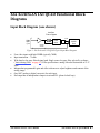
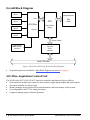


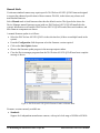


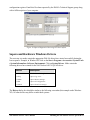
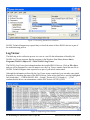
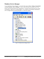
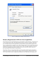
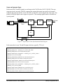


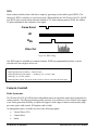


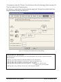

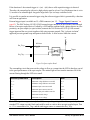
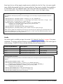


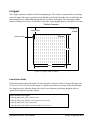
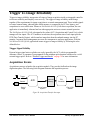
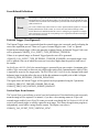


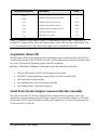


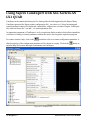


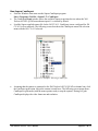

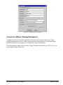


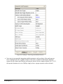
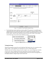

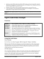


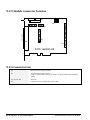
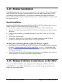
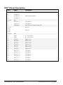


![[Insert the picture here]](http://vs1.manualzilla.com/store/data/005750886_1-61b7896b0a61bec1f004b64a994fc9d3-150x150.png)