1
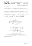
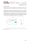
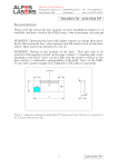
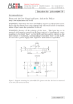
Quantum Cascade Solutions
Passage Max.-Meuron 1-3 CH-2000 Neuchˆatel
Case Postale 1766
Switzerland
Tel: +41 32 729 95 10
Fax: +41 32 721 36 19
Datasheet for #sb554 DN
Recommendations:
Please read the starter kit user manual (at least installation chapter 5), if
available, and have a look at the FAQ at http://www.alpeslasers.ch/alfaq.pdf
WARNING: Operating the laser with longer pulses, shorter period, or
higher voltage or current than specified in this document may cause damage
and will result in loss of warranty, unless agreed upon with Alpes Lasers!
WARNING: Beware of the polarity of the laser. This laser has to be powered with negative bias on the laser contact (= bonding pad, corresponding
to the label ”laser” on the LLH) and the positive bias on the base contact
(= submount, corresponding to the label ”base” on the LLH).
Emission
DN
UP
Figure 1: Support mounting for #sb554 DN (please note that the laser is connected to
the DN pad drawned in blue)
1
#sb554 DN
#sb554 DN
4
-30C
-15C
0C
15C
30C
3.5
3
P [mW]
2.5
2
1.5
1
0.5
0
-0.5
1711
1712
1713
1714
1715 1716 1717
Frequency [cm-1]
1718
1719
1720
Figure 2: Output power as a function of the singlemode emission frequencies and temperatures
#sb554 DN
10.5
-30C
-15C
0C
15C
30C
10
9.5
Uldd [V]
9
8.5
8
7.5
7
6.5
1711
1712
1713
1714 1715 1716 1717
Frequency [cm-1]
1718
1719
1720
Figure 3: DC voltage fed to LDD (Uldd) as a function of the singlemode emission frequencies and temperatures
2
#sb554 DN
λ[nm] ν[cm−1 ]
5814.8 1719.7
5815.3 1719.6
5815.8 1719.4
5816.3 1719.3
5823.1 1717.3
5823.4 1717.2
5823.7 1717.1
5828.4 1715.7
5828.8 1715.6
5829.1 1715.5
5829.2 1715.5
5834.9 1713.8
5835.4 1713.7
5836
1713.5
5836.7 1713.3
5841.4 1711.9
5841.9 1711.8
5842.5 1711.6
5843.2 1711.4
P[mW]
0
0.7
2.4
3.8
1.7
2.5
3.3
0
0.5
1.8
2.4
0.1
0.4
1.7
2.8
0
0.2
1.3
2.2
Temp[◦ C] ULDD [V]
-30
7
-30
8
-30
9
-30
10
-15
9
-15
9.5
-15
10
0
7
0
8
0
9
0
9.5
15
7
15
8
15
9
15
10
30
7
30
8
30
9
30
10
Ipulse [A]
0.19
0.34
0.52
0.68
0.54
0.61
0.7
0.22
0.38
0.57
0.64
0.27
0.42
0.58
0.74
0.26
0.41
0.57
0.71
Table 1 : singlemode optical output power as function of operating parameters
#sb554 DN
power (-30C )
voltage (-30C )
power (-15C )
voltage (-15C )
power (0C )
voltage (0C )
power (15C )
voltage (15C )
power (30C )
voltage (30C )
Max single mode power
7
Peak Voltage [V]
6
5
3.5
3
2.5
2
4
1.5
3
1
2
0.5
1
0
0
0
0.1
0.2
0.3
0.4
0.5
Peak Current [A]
0.6
0.7
Light [mW] avg on power meter
8
-0.5
0.8
Figure 4: peak voltage and average power vs peak current at 2% dc (the solid squares
indicate the maximum singlemode emitted power)
3
#sb554 DN
#sb554 DN
7
6
Peak Voltage [V]
4
power (-30C )
voltage (-30C )
power (-15C )
voltage (-15C )
power (0C )
voltage (0C )
power (15C )
voltage (15C )
power (30C )
voltage (30C )
Max single mode power
5
3.5
3
2.5
2
4
1.5
3
1
2
0.5
1
0
Light [mW] avg on power meter
8
0
0
0.1
0.2
0.3
0.4
0.5
Peak Current [A]
0.6
0.7
-0.5
0.8
Figure 5: peak voltage and average power vs peak current at 2% dc (including the multimode region)
Note: data taken with 50ns pulses, 2.5µs period.
#sb554 DN
power (-30C )
current (-30C )
power (-15C )
current (-15C )
power (0C )
current (0C )
power (15C )
current (15C )
power (30C )
current (30C )
Max single mode power
0.7
Peak Current [A]
0.6
0.5
3.5
3
2.5
2
0.4
1.5
0.3
1
0.2
0.5
0.1
0
0
0
2
4
6
DC Voltage fed to LDD [V]
8
Light [mW] avg on power meter
0.8
-0.5
10
Figure 6: peak current and average power vs LDD voltage at 2% dc (the solid squares
indicate the maximum singlemode emitted power)
4
#sb554 DN
#sb554 DN
0.7
0.6
Peak Current [A]
4
power (-30C )
current (-30C )
power (-15C )
current (-15C )
power (0C )
current (0C )
power (15C )
current (15C )
power (30C )
current (30C )
Max single mode power
0.5
3.5
3
2.5
2
0.4
1.5
0.3
1
0.2
0.5
0.1
0
Light [mW] avg on power meter
0.8
0
0
2
4
6
DC Voltage fed to LDD [V]
-0.5
10
8
Figure 7: peak current and average power vs LDD voltage at 2% dc (including the multimode region)
Spectral density (normalized to 1)
30C 7.0V
30C 8.0V
30C 9.0V
30C 10.0V
15C 7.0V
15C 8.0V
15C 9.0V
15C 10.0V
0C 10.0V
0C 7.0V
0C 9.0V
8.0V
0C
0C
9.5V
-15C 9.5V
9.0V
-15C
-15C 10.0V
1.2
-30C 7.0V
-30C 8.0V
-30C 9.0V
-30C 10.0V
#sb554 DN
1
0.8
0.6
0.4
0.2
0
-0.2
5810
5815
5820
5825
5830 5835 5840
Wavelength [nm]
5845
5850
5855
Figure 8: spectra at -30C, -15C, 0C, 15C and 30C at 2% dc for various LDD voltages
5
#sb554 DN
Spectral density (normalized to 1)
-30C 10.0V
-30C 9.0V
-30C 7.0V
1.2
-30C 8.0V
#sb554 DN
1
0.8
0.6
0.4
0.2
0
-0.2
5813
5814
5815
5816
5817
Wavelength [nm]
5818
5819
Figure 9: spectra at -30C for various LDD voltages
Spectral density (normalized to 1)
-15C 10.0V
-15C 9.0V
1.2
-15C 9.5V
#sb554 DN
1
0.8
0.6
0.4
0.2
0
-0.2
5821
5822
5823
5824
Wavelength [nm]
5825
5826
Figure 10: spectra at -15C for various LDD voltages
6
#sb554 DN
Spectral density (normalized to 1)
0C 10.0V
0C 9.5V
0C 9.0V
0C 7.0V
1.2
0C 8.0V
#sb554 DN
1
0.8
0.6
0.4
0.2
0
-0.2
5827
5828
5829
5830
5831
Wavelength [nm]
5832
5833
Figure 11: spectra at 0C for various LDD voltages (hole in spectrum at 10V due to
absorption in the air)
Spectral density (normalized to 1)
15C 10.0V
15C 9.0V
15C 7.0V
1.2
15C 8.0V
#sb554 DN
1
0.8
0.6
0.4
0.2
0
-0.2
5833
5834
5835
5836
5837
Wavelength [nm]
5838
5839
5840
Figure 12: spectra at 15C for various LDD voltages
7
#sb554 DN
Spectral density (normalized to 1)
30C 10.0V
30C 9.0V
30C 7.0V
1.2
30C 8.0V
#sb554 DN
1
0.8
0.6
0.4
0.2
0
-0.2
5840
5841
5842
5843
5844
Wavelength [nm]
5845
5846
Figure 13: spectra at 30C for various LDD voltages
8
#sb554 DN