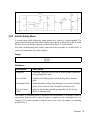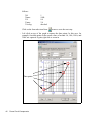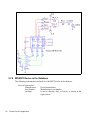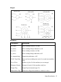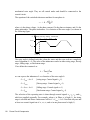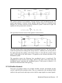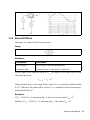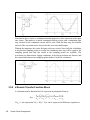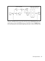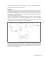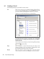
1
PSIM
User’s Guide
Powersim Inc.
-9
PSIM User’s Guide
Version 7.0
Release 4
June 2006
Copyright © 2001-2006 Powersim Inc.
All rights reserved. No part of this manual may be photocopied or reproduced in any form or by any
means without the written permission of Powersim Inc.
Disclaimer
Powersim Inc. (“Powersim”) makes no representation or warranty with respect to the adequacy or
accuracy of this documentation or the software which it describes. In no event will Powersim or its
direct or indirect suppliers be liable for any damages whatsoever including, but not limited to, direct,
indirect, incidental, or consequential damages of any character including, without limitation, loss of
business profits, data, business information, or any and all other commercial damages or losses, or for
any damages in excess of the list price for the licence to the software and documentation.
Powersim Inc.
email: [email protected]
http://www.powersimtech.com
-8
Contents
1
2
General Information
1.1
Introduction 1
1.2
Circuit Structure 2
1.3
Software/Hardware Requirement 3
1.4
Installing the Program 3
1.5
Simulating a Circuit 4
1.6
Component Parameter Specification and Format 4
Power Circuit Components
2.1
Resistor-Inductor-Capacitor Branches 7
2.1.1 Resistors, Inductors, and Capacitors 7
2.1.2 Rheostat 8
2.1.3 Saturable Inductor 9
2.1.4 Nonlinear Elements 10
2.2
Switches 11
2.2.1 Diode, DIAC, and Zener Diode 12
2.2.2 Thyristor and TRIAC 13
2.2.3 GTO, Transistors, and Bi-Directional Switch 15
2.2.4 Linear Switches 17
2.2.5 Switch Gating Block 19
2.2.6 Single-Phase Switch Modules 21
2.2.7 Three-Phase Switch Modules 22
2.3
Coupled Inductors 24
2.4
Transformers 26
2.4.1 Ideal Transformer 26
i -7
2.4.2 Single-Phase Transformers 26
2.4.3 Three-Phase Transformers 29
2.5
Magnetic Elements 30
2.5.1 Winding 30
2.5.2 Leakage Flux Path 31
2.5.3 Air Gap 32
2.5.4 Linear Core 34
2.5.5 Saturable Core 34
2.6
Other Elements 36
2.6.1 Operational Amplifier 36
2.6.2 dv/dt Block 37
2.6.3 Power Modeling Block 38
2.7
2.8
-6
ii
Thermal Module 39
2.7.1
Device Database Editor 39
2.7.2
Diode Device in the Database 48
2.7.3
Diode Loss Calculation 49
2.7.4
IGBT Device in the Database 51
2.7.5
IGBT Loss Calculation 53
2.7.6
MOSFET Device in the Database 56
2.7.7
MOSFET Loss Calculation 58
Motor Drive Module 61
2.8.1
Reference Direction of Mechanical Systems 61
2.8.2
DC Machine 64
2.8.3
Induction Machine 66
2.8.4
Induction Machine with Saturation 70
2.8.5
Brushless DC Machine 72
2.8.6
Synchronous Machine with External Excitation 77
2.8.7
Permanent Magnet Synchronous Machine 80
2.8.8
Permanent Magnet Synchronous Machine with Saturation 83
2.8.9
Switched Reluctance Machine 87
2.9
MagCoupler Module 90
2.10
MagCoupler-RT Module 95
2.11
Mechanical Elements and Sensors 98
2.11.1 Mechanical Elements and Sensors 98
2.11.1.1 Constant-Torque Load 98
2.11.1.2 Constant-Power Load 99
2.11.1.3 Constant-Speed Load 100
2.11.1.4 General-Type Load 100
2.11.1.5 Externally-Controlled Load 101
2.11.2 Gear Box 101
2.11.3 Mechanical Coupling Block 102
2.11.4 Mechanical-Electrical Interface Block 102
2.11.5 Speed/Torque Sensors 105
2.11.6 Position Sensors 107
2.11.6.1 Absolute Encoder 108
2.11.6.2 Incremental Encoder 108
2.11.6.3 Resolver 109
2.11.6.4 Hall-Effect Sensor 110
3
Control Circuit Components
3.1
Transfer Function Blocks 111
3.1.1 Proportional Controller 112
3.1.2 Integrator 113
3.1.3 Differentiator 115
3.1.4 Proportional-Integral Controller 115
3.1.5 Built-in Filter Blocks 116
3.2
Computational Function Blocks 117
3.2.1 Summer 117
3.2.2 Multiplier and Divider 118
3.2.3 Square-Root Block 118
3.2.4 Exponential/Power/Logarithmic Function Blocks 119
3.2.5 Root-Mean-Square Block 119
3.2.6 Absolute and Sign Function Blocks 120
3.2.7 Trigonometric Functions 120
iii-5
3.2.8 Fast Fourier Transform Block 121
3.3
Other Function Blocks 122
3.3.1 Comparator 122
3.3.2 Limiter 122
3.3.3 Gradient (dv/dt) Limiter 123
3.3.4 Trapezoidal and Square Blocks 123
3.3.5 Sampling/Hold Block 124
3.3.6 Round-Off Block 125
3.3.7 Time Delay Block 126
3.3.8 Multiplexer 127
3.3.9 THD Block 128
3.4
Logic Components 129
3.4.1 Logic Gates 129
3.4.2 Set-Reset Flip-Flop 130
3.4.3 J-K Flip-Flop 131
3.4.4 D Flip-Flop 131
3.4.5 Monostable Multivibrator 132
3.4.6 Pulse Width Counter 132
3.4.7 Up/Down Counter 133
3.4.8 A/D and D/A Converters 134
3.5
Digital Control Module 135
3.5.1 Zero-Order Hold 135
3.5.2 z-Domain Transfer Function Block 136
3.5.2.1 Integrator 138
3.5.2.2 Differentiator 139
3.5.2.3 Digital Filters 140
3.5.3 Unit Delay 143
3.5.4 Quantization Block 143
3.5.5 Circular Buffer 144
3.5.6 Convolution Block 145
3.5.7 Memory Read Block 146
3.5.8 Data Array 146
3.5.9 Stack 148
-4
iv
3.5.10 Multi-Rate Sampling System 148
3.6
SimCoupler Module 150
3.6.1 Set-up in PSIM and Simulink 150
3.6.2 Solver Type and Time Step Selection in Simulink 153
4
Other Components
4.1
Parameter File 157
4.2
Sources 158
4.2.1 Time 158
4.2.2 DC Source 158
4.2.3 Sinusoidal Source 159
4.2.4 Square-Wave Source 160
4.2.5 Triangular Source 161
4.2.6 Step Sources 162
4.2.7 Piecewise Linear Source 163
4.2.8 Random Source 165
4.2.9 Math Function Source 165
4.2.10 Voltage/Current-Controlled Sources 166
4.2.11 Nonlinear Voltage-Controlled Sources 168
4.3
Voltage/Current Sensors 169
4.4
Probes and Meters 169
4.5
Voltage/Current Scopes 172
4.6
Switch Controllers 174
4.6.1 On-Off Switch Controller 174
4.6.2 Alpha Controller 175
4.6.3 PWM Lookup Table Controller 176
4.7
Function Blocks 179
4.7.1 Control-Power Interface Block 179
4.7.2 ABC-DQO Transformation Block 180
4.7.3 Math Function Blocks 181
v -3
4.7.4 Lookup Tables 182
4.7.5 C Script Block 185
4.7.6 External DLL Blocks 186
4.7.7 Embedded Software Block 191
5
6
Analysis Specification
5.1
Transient Analysis 193
5.2
AC Analysis 194
5.3
Parameter Sweep 198
Circuit Schematic Design
6.1
Creating a Circuit 202
6.2
Editing a Circuit 203
6.3
Saving a File 206
6.4
Subcircuit 207
6.4.1 Creating Subcircuit - In the Main Circuit 208
6.4.2 Creating Subcircuit - Inside the Subcircuit 208
6.4.3 Connecting Subcircuit - In the Main Circuit 210
6.4.4 Other Features of the Subcircuit 210
6.4.4.1 Passing Variables from the Main Circuit to Subcircuit 211
6.4.4.2 Customizing the Subcircuit Image 212
6.4.4.3 Including Subcircuits in the PSIM Element List 213
6.5
Running the Simulation 214
6.6
Managing the PSIM Library 218
6.7
Other Options 223
6.7.1 Generate and View the Netlist File 223
6.7.2 Set Path 223
6.7.3 Settings 224
6.7.4 Printing the Circuit Schematic 224
-2
vi
7
8
Waveform Processing
7.1
File Menu 226
7.2
Edit Menu 226
7.3
Axis Menu 227
7.4
Screen Menu 228
7.5
View Menu 230
7.6
Option Menu 231
7.7
Label Menu 231
7.8
Exporting Data 231
Error/Warning Messages and Other Simulation Issues
8.1
Simulation Issues 233
8.1.1 Time Step Selection 233
8.1.2 Propagation Delays in Logic Circuits 233
8.1.3 Interface Between Power and Control Circuits 234
8.1.4 FFT Analysis 234
8.2
Error/Warning Messages 235
8.3
Debugging 236
vii-1
0viii
1
General Information
1.1
Introduction
PSIM is a simulation software specifically designed for power electronics and motor
drives. With fast simulation and friendly user interface, PSIM provides a powerful
simulation environment for power electronics, analog and digital control, magnetics,
and motor drive system studies.
This manual covers both PSIM1 and the following add-on Modules:
Motor Drive Module
Digital Control Module
SimCoupler Module
Thermal Module
MagCoupler Module
MagCoupler-RT Module
The Motor Drive Module has built-in machine models and mechanical load models for
motor drive system studies.
The Digital Control Module provides discrete elements such as zero-order hold, zdomain transfer function blocks, quantization blocks, digital filters, for digital control
system analysis.
The SimCoupler Module provides interface between PSIM and Matlab/Simulink2 for
co-simulation.
The Thermal Module provides the capability to calculate semiconductor devices losses.
The MagCoupler Module provides interface between PSIM and the electromagnetic
field analysis software JMAG3 for co-simulation.
The MagCoupler-RT Module links PSIM with JMAG-RT3 data files.
In addition, PSIM supports links to third-party software through custom DLL blocks.
The overall PSIM environment is shown below.
1. PSIM and SIMVIEW are copyright by Powersim Inc., 2001-2006
2. Matlab and Simulink are registered trademarks of the MathWorks, Inc.
3. JMAG and JMAG-RT are copyright by the Japan Research Institute, Ltd., 1997-2006
Introduction
1
Third-party
Software
Matlab/Simulink
- Control systems
PSIM
- Power electronics
- Analog/digital control
- Motor drives
JMAG /
JMAG-RT
- Finite element analysis
- Electric machines, and
other magnetic devices
The PSIM simulation environment consists of the circuit schematic program PSIM, the
simulator engine, and the waveform processing program SIMVIEW1. The simulation
process is illustrated as follows.
PSIM Schematic
Circuit Schematic Editor (input: *.sch)
PSIM Simulator
PSIM Simulator (output: *.smv or *.txt)
SIMVIEW
Waveform Processor (input: *.smv or *.txt)
Chapter 1 of this manual describes the circuit structure, software/hardware requirement,
and parameter specification format. Chapter 2 through 4 describe the power and control
circuit components. Chapter 5 describes the specifications of the transient analysis and
ac analysis. The use of the PSIM schematic program and SIMVIEW is discussed in
Chapter 6 and 7. Finally, error/warning messages are discussed in Chapter 8.
1.2
Circuit Structure
A circuit is represented in PSIM in four blocks: power circuit, control circuit, sensors,
and switch controllers. The figure below shows the relationship between these blocks.
2
General Information
Power Circuit
Switch
Controllers
Sensors
Control Circuit
The power circuit consists of switching devices, RLC branches, transformers, and
coupled inductors. The control circuit is represented in block diagram. Components in s
domain and z domain, logic components (such as logic gates and flip flops), and
nonlinear components (such as multipliers and dividers) are used in the control circuit.
Sensors are used to measure power circuit quantities and pass them to the control
circuit. Gating signals are then generated from the control circuit and sent back to the
power circuit through switch controllers to control switches.
1.3
Software/Hardware Requirement
PSIM runs in Microsoft Windows environment 2000/XP on personal computers. The
minimum RAM memory requirement is 128 MB.
1.4
Installing the Program
A quick installation guide is provided in the flier “PSIM - Quick Guide” and on the CDROM.
Some of the files in the PSIM directory are shown in the table below.
Files
Description
PSIM.exe
PSIM circuit schematic editor
SIMVIEW.exe
Waveform display program SIMVIEW
PcdEditor.exe
Device database editor
s2z_converter.exe
s-domain to z-domain converter
Software/Hardware Requirement
3
SetSimPath.exe
Program to set up the SimCoupler
Module
psim.lib, psimimage.lib
PSIM library files
File extensions used in PSIM are:
1.5
*.sch
PSIM schematic file
*.txt
PSIM simulation output file (text)
*.fra
PSIM ac analysis output file (text)
*.dev
Device database file
*.smv
SIMVIEW data file
Simulating a Circuit
To simulate the sample one-quadrant chopper circuit “chop.sch”:
- Start PSIM. From the File menu, choose Open to load the file “chop.sch”.
- From the Simulate menu, choose Run PSIM to start the simulation.
Simulation results will be saved to File “chop.txt”.
- If the option Auto-run SIMVIEW is not selected in the Options menu, from
the Simulate menu, choose Run SIMVIEW to start SIMVIEW. If the option
is selected, SIMVIEW will be launched automatically. In SIMVIEW, select
curves for display.
1.6
Component Parameter Specification and Format
The parameter dialog window of each component in PSIM has three tabs: Parameters,
Other Info, and Color, as shown below.
The parameters in the Parameters tab are used in the simulation. The information in the
4
General Information
Other Info tab, on the other hand, is not used in the simulation. It is for reporting
purposes only and will appear in the parts list in View -> Element List in PSIM.
Information such as device rating, manufacturer, and part number can be stored under
the Other Info tab.
The component color can be set in the Color tab.
Parameters under the Parameters tab can be a numerical value or a mathematical
expression. A resistance, for example, can be specified in one of the following ways:
12.5
12.5k
12.5Ohm
12.5kOhm
25./2.Ohm
R1+R2
R1*0.5+(Vo+0.7)/Io
where R1, R2, Vo, and Io are symbols defined either in a parameter file (see Section
4.1), or in a main circuit if this resistor is in a subcircuit (see Section 6.3.4.1).
Power-of-ten suffix letters are allowed in PSIM. The following suffix letters are
supported:
G
M
k or K
m
u
n
p
109
106
103
10-3
10-6
10-9
10-12
A mathematical expression can contain brackets and is not case sensitive. The following
mathematical functions are allowed:
+
*
/
^
SQRT
SIN
COS
addition
subtraction
multiplication
division
to the power of [Example: 2^3 = 2*2*2]
square-root function
sine function
cosine function
Component Parameter Specification and Format
5
6
ASIN
ACOS
TAN
ATAN
ATAN2
SINH
COSH
sine inverse function
cosine inverse function
tangent function
inverse tangent function
inverse tangent function [-π <= atan2(y,x) <= π]
hyperbolic sine function
hyperbolic cosine function
EXP
LOG
LOG10
ABS
SIGN
exponential (base e) [Example: EXP(x) = ex]
logarithmic function (base e) [Example: LOG(x) = ln (x)]
logarithmic function (base 10)
absolute function
sign function [Example: SIGN(1.2) = 1; SIGN(-1.2)=-1]
General Information
2
Power Circuit Components
2.1
Resistor-Inductor-Capacitor Branches
2.1.1 Resistors, Inductors, and Capacitors
Both individual resistor, inductor, capacitor, and lumped RLC branches are provided in
PSIM. Initial conditions of inductor currents and capacitor voltages can be defined.
To facilitate the setup of three-phase circuits, symmetrical three-phase RLC branches,
“R3”, “RL3”, “RC3”, “RLC3”, are provided. Initial inductor currents and capacitor
voltages of the three-phase branches are all zero.
Images:
R
L
C
R3
RC
RL
RL3
RC3
LC
RLC3
RLC
For three-phase branches, the phase with a dot is Phase A.
Attributes:
Parameters
Description
Resistance
Resistance, in Ohm
Inductance
Inductance, in H
Capacitance
Capacitance, in F
Initial Current
Initial inductor current, in A
Initial Cap. Voltage
Initial capacitor voltage, in V
Resistor-Inductor-Capacitor Branches
7
Current Flag
Flag for branch current output.
If the flag is zero, there is no current output. If the flag is
1, the current will be available for display in the runtime
graphs (under Simulate -> Runtime Graphs). It will also
be saved to the output file for display in SIMVIEW.
The current is positive when it flows into the dotted
terminal of the branch.
Current Flag_A;
Current Flag_B;
Current Flag_C
Current flags for Phase A, B, and C of three-phase
branches, respectively.
The resistance, inductance, or capacitance of a branch can not be all zero. At least one of
the parameters has to be a non-zero value.
2.1.2 Rheostat
A rheostat is a resistor with a tap.
Image:
t
k
m
Attributes:
8
Parameters
Description
Total Resistance
Total resistance of the rheostat R (between Node k and m),
in Ohm
Tap Position (0 to 1)
The tap position Tap. The resistance between Node k and t
is: R*Tap.
Current Flag
Flag for the current that flows into Node k.
Power Circuit Components
2.1.3 Saturable Inductor
A saturable inductor takes into account the saturation effect of the magnetic core.
Image:
Attributes:
Parameters
Description
Current v.s. Inductance
Characteristics of the current versus the inductance (i1,
L1), (i2, L2), etc.
Current Flag
Flag for the current display
The nonlinear B-H curve is represented by piecewise linear approximation. Since the
flux density B is proportional to the flux linkage λ and the magnetizing force H is
proportional to the current i, the B-H curve can be represented by the λ-i curve instead,
as shown below.
λ3
λ2
λ1
λ (B)
Inductance L = λ / i
i1
i2
i3
i (H)
The inductance is defined as: L = λ / i, the ratio of λ v.s. i at each point. The saturation
characteristics are defined by a series of data points as: (i1, L1), (i2, L2), (i3, L3), etc.
Note that the defined saturation characteristics must be such that the flux linkage λ is
monotonically increasing. That is, L1*i1 < L2*i2 < L3*i3, etc.
Also, similar to the saturation characteristics in the real world, the slope of each linear
segment must be monotonically decreasing as the current increases.
In certain situations, circuits that contain saturable inductors may fail to converge.
Connecting a very small capacitor across the saturable inductor may help the
convergence.
Resistor-Inductor-Capacitor Branches
9
2.1.4 Nonlinear Elements
The following elements with nonlinear voltage-current relationship are provided:
- Resistance-type [v = f(i)]
- Resistance-type with additional input x [v = f(i,x)]
- Conductance-type [i = f(v)]
- Conductance-type with additional input x [i = f(v,x)]
The additional input x must be a voltage signal.
Images:
Nonlinear element
Nonlinear element (with additional input)
Input x
Attributes:
For resistance-type elements:
Parameters
Description
Expression f(i) or f(i,x)
Expression of v in terms of i and x [v = f(i) or v = f(i,x)]
Expression df/di
The derivative of the voltage v versus current i, i.e. df(i)/di
Initial Value io
The initial value of the current i
Lower Limit of i
The lower limit of the current i
Upper Limit of i
The upper limit of the current i
For conductance-type elements:
10
Parameters
Description
Expression f(v) or f(v,x)
Expression of i in terms of v and x [i = f(v) or i = f(v,x)]
Expression df/dv
Derivative of the current i versus voltage v, i.e. df(v)/dv
Initial Value vo
The initial value of the voltage v
Lower Limit of v
The lower limit of the voltage v
Upper Limit of v
The upper limit of the voltage v
Power Circuit Components
A good initial value and lower/upper limits will help the convergence of the solution.
Example: Nonlinear Diode
The nonlinear element (NONI) in the circuit above models a nonlinear diode. The diode
current is expressed as a function of the voltage as: i = 10-14 * (e 40*v-1). In PSIM, the
specifications of the nonlinear element will be:
2.2
Expression f(v)
1e-14*(EXP(40*v)-1)
Expression df/dv
40e-14*EXP(40*v)
Initial Value vo
0
Lower Limit of v
-1e3
Upper Limit of v
1
Switches
There are two basic types of switches in PSIM. One is the switchmode type. It operates
either in the cut-off region (off state) or saturation region (on state). The other is the
linear type. It can operates in either cut-off, linear, or saturation region.
Switches in switchmode include the following:
- Diode and DIAC
- Thyristor and TRIAC
- Self-commutated switches, specifically:
- Gate-Turn-Off switch
- npn bipolar junction transistor
- pnp bipolar junction transistor
- Insulated-Gate Bipolar Transistor (IGBT)
- n-channel Metal-Oxide-Semiconductor Field-Effect Transistor
(MOSFET) and p-channel MOSFET
- Bi-directional switch
Switches
11
Switch models are ideal. That is, both turn-on and turn-off transients are neglected. A
switch has an on-resistance of 10μΩ and an off-resistance of 10MΩ. Snubber circuits
are not required for switches.
Linear switches include the following:
- npn bipolar junction transistor
- pnp bipolar junction transistor
2.2.1 Diode, DIAC, and Zener Diode
The conduction of a diode is determined by circuit operating conditions. A diode is
turned on when it is positively biased, and is turned off when the current drops to zero.
Image:
Attributes:
Parameters
Description
Diode Voltage Drop
Diode conduction voltage drop, in V
Initial Position
Flag for the initial diode position. If the flag is 0, the diode
is off. If it is 1, the diode is on.
Current Flag
Current flag of the diode.
A DIAC is a bi-directional diode. A DIAC does not conduct until the breakover voltage
is reached. After that, the DIAC goes into avalanche conduction, and the conduction
voltage drop is the breakback voltage.
Image:
Attributes:
12
Parameters
Description
Breakover Voltage
Voltage at which breakover occurs and the DIAC begins to
conduct, in V
Power Circuit Components
Breakback Voltage
Conduction voltage drop, in V
Current Flag
Current flag
A zener diode is modelled by a circuit as shown below.
Images:
K
Zener
Circuit Model
K
VB
A
A
Attributes:
Parameters
Description
Breakdown Voltage
Breakdown voltage VB of the zener diode, in V
Forward Voltage Drop
Voltage drop of the forward conduction (diode voltage
drop from anode to cathode), in V
Current Flag
Flag for zener current output (from anode to cathode)
When the zener diode is positively biased, it behaviors as a regular diode. When it is
reverse biased, it will block the conduction as long as the cathode-anode voltage VKA is
less than the breakdown voltage VB. When VKA exceeds VB, the voltage VKA will be
clamped to VB. [Note: when the zener is clamped, since the diode is modelled with an
on-resistance of 10μΩ, the cathode-anode voltage will in fact be equal to: VKA = VB +
10μΩ * IKA. Therefore, depending on the value of IKA, VKA will be slightly higher than
VB. If IKA is very large, VKA can be substantially higher than VB].
2.2.2 Thyristor and TRIAC
A thyristor is controlled at turn-on. The turn-off is determined by circuit conditions.
A TRIAC is a device that can conduct current in both directions. It behaviors in the
same way as two opposite thyristors connected in parallel.
Switches
13
Images:
Thyristor
A
TRIAC
K
Gate
Gate
Attributes:
Parameters
Description
Voltage Drop
Thyristor conduction voltage drop, in V
Holding Current
Minimum conduction current below which the device stops
conducting and returns to the OFF state (for thyristor only)
Latching Current
Minimum ON state current required to keep the device in the
ON state after the triggering pulse is removed (for thyristor
only)
Initial Position
Flag for the initial switch position (for thyristor only)
Current Flag
Flag for switch current output
Note that for the TRIAC device, the holding current and latching current are set to zero.
There are two ways to control a thyristor or TRIAC. One is to use a gating block, and
the other is to use a switch controller. The gate node of a thyristor or TRIAC must be
connected to either a gating block or a switch controller.
The following examples illustrate the control of a thyristor switch.
Examples: Control of a Thyristor Switch
Gating Block
Alpha
Controller
14
Power Circuit Components
This circuit on the left uses a switching gating block. The switching gating pattern and
the frequency are pre-defined, and remain unchanged throughout the simulation. The
circuit on the right uses an alpha switch controller. The delay angle alpha, in deg., is
specified through the dc source in the circuit.
2.2.3 GTO, Transistors, and Bi-Directional Switch
Self-commutated switches in the switchmode, except pnp bipolar junction transistor
(BJT) and p-channel MOSFET, are turned on when the gating signal is high (when a
voltage of 1V or higher is applied to the gate node) and the switch is positively biased
(collector-emitter or drain-source voltage is positive). It is turned off whenever the
gating signal is low or the current drops to zero.
For pnp BJT and p-channel MOSFET, switches are turned on when the gating signal is
low and switches are negatively biased (collector-emitter or drain-source voltage is
negative).
A GTO switch is a symmetrical device with both forward-blocking and reverse-blocking
capabilities. An IGBT or MOSFET switch consist of an active switch with an antiparallel diode.
A bi-directional switch conducts currents in both directions. It is on when the gating
signal is high and is off when the gating signal is low, regardless of the voltage bias
conditions.
Note that a limitation of the BJT switch model in PSIM, in contrary to the device
behavior in the real life, is that a BJT switch in PSIM will block reverse voltage (in this
sense, it behaviors like a GTO). Also, it is controlled by a voltage signal at the gate node,
not a current.
Images:
GTO
BJT(
(npn)
BJT
(pnp)
MOSFET
(n-channel)
MOSFET
(p-channel)
IGBT
Bi-directional
switch
Switches
15
Attributes:
Parameters
Description
Initial Position
Initial switch position flag. For MOSFET and IGBT, this
flag is for the active switch, not for the anti-parallel diode.
Current Flag
Switch current flag. For MOSFET and IGBT, the current
through the whole module (the active switch plus the diode)
will be displayed.
A switch can be controlled by either a gating block or a switch controller. They must be
connected to the gate (base) node of the switch. The following examples illustrate the
control of a MOSFET switch.
Examples: Control of a MOSFET Switch
On-off Controller
The circuit on the left uses a gating block, and the one on the right uses an on-off switch
controller. The gating signal is determined by the comparator output.
Example: Control of a npn Bipolar Junction Transistor
The circuit on the left uses a gating block, and the one on the right uses an on-off switch
controller.
16
Power Circuit Components
The following shows another example of controlling the BJT switch. The circuit on the
left shows how a BJT switch is controlled in the real life. In this case, the gating voltage
VB is applied to the transistor base drive circuit through a transformer, and the base
current determines the conduction state of the transistor.
This circuit can be modelled and implemented in PSIM as shown on the right. A diode,
Dbe, with a conduction voltage drop of 0.7V, is used to model the pn junction between
the base and the emitter. When the base current exceeds 0 (or a certain threshold value,
in which case the base current will be compared to a dc source), the comparator output
will be 1, applying the turn-on pulse to the transistor through the on-off switch
controller.
2.2.4 Linear Switches
Linear switches include npn bipolar junction transistor and pnp bipolar junction
transistor. They can operate in either cut-off, linear, or saturation region.
Images:
BJT (npn)
BJT (pnp)
Switches
17
Attributes:
Parameters
Description
Current Gain beta
Transistor current gain β, defined as: β=Ic/Ib
Bias Voltage Vr
Forward bias voltage, in V, between base and emitter for
the npn transistor, or between emitter and base for the pnp
transistor.
Vce,sat [or Vec,sat for
pnp]
Saturation voltage, in V, between collector and emitter for
the npn transistor, and between emitter and collector for
the pnp transistor.
A linear BJT switch is controlled by the base current Ib. It can operate in one of the three
regions: cut-off (off state), linear, and saturation region (on state). The properties of
these regions for the npn transistor are:
Ic = 0
- Cut-off region: Vbe < Vr; Ib = 0;
- Linear region:
Vbe = Vr; Ic = β∗Ib; Vce > Vce,sat
- Saturation region: Vbe = Vr; Ic < β∗Ib; Vce = Vce,sat
where Vbe is the base-emitter voltage, Vce is the collector-emitter voltage, and Ic is the
collector current.
Note that for both the npn and pnp transistors, the gate node (base node) is a power
node, and must be connected to a power circuit component (such as a resistor or a
source). It can not be connected to a gating block or a switch controller.
WARNING: It has been found that the linear model for npn and pnp
transistors works well in simple circuits, but may not work when
circuits are complex. Please use this model with caution.
Examples: Circuits Using the Linear BJT Switch
Examples below illustrate the use of linear switches. The circuit on the left is a linear
voltage regulator circuit, and the transistor operates in the linear mode. The circuit on
the right is a simple test circuit.
18
Power Circuit Components
NPN_1
NPN_1
2.2.5 Switch Gating Block
A switch gating block defines the gating pattern of a switch or a switch module. The
gating pattern can be specified either directly (the element is called Gating Block in the
library) or in a text file (the element is called Gating Block (1) in the library).
Note that a switch gating block can be connected to the gate node of a switch ONLY. It
can not be connected to any other elements.
Image:
Attributes:
Parameters
Description
Frequency
Operating frequency of the switch or switch module connected
to the gating block, in Hz
No. of Points
Number of switching points (for the Gating Block element
only)
Switching Points
Switching points, in deg. If the frequency is zero, the switching
points is in second. (for the Gating Block element only)
File for Gating
Table
Name of the file that stores the gating table (for the Gating
Block (1) element only)
The number of switching points is defined as the total number of switching actions in
one period. Each turn-on or turn-off action is counted as one switching point. For
example, if a switch is turned on and off once in one cycle, the number of switching
points will be 2.
Switches
19
For the Gating Block (1) element, the file for the gating table must be in the same
directory as the schematic file. The gating table file has the following format:
n
G1
G2
... ...
Gn
where G1, G2, ..., Gn are the switching points.
Example:
Assume that a switch operates at 2000 Hz and has the following gating pattern in one
period:
35
92
0
175
187
180
345
357
360
(deg.)
The specification of the Gating Block element for this switch will be:
Frequency
2000.
No. of Points
6
Switching Points
35. 92. 175. 187. 345. 357.
The gating pattern has 6 switching points (3 pulses). The corresponding switching
angles are 35o, 92o, 175o, 187o, 345o, and 357o, respectively.
If the Gating Block (1) element is used instead, the specification will be:
Frequency
2000.
File for Gating Table
test.tbl
The file “test.tbl” will contain the following:
6
35.
92.
175.
187.
20
Power Circuit Components
345.
357.
2.2.6 Single-Phase Switch Modules
Built-in single-phase diode bridge module and thyristor bridge module are provided.
The images and internal connections of the modules are shown below.
Images:
Diode bridge
A+
Thyristor bridge
DC+
1
3
DC+
DC+
A+
A+
A-
A-
DC-
4
DC-
Ct
3
DC+
A-
A-
2
1
A+
DC-
4
2
Ct
DC-
Attributes:
Parameters
Description
Diode Voltage Drop or
Voltage Drop
Forward voltage drop of each diode or thyristor, in V
Init. Position_i
Initial position for Switch i
Current Flag_i
Current flag for Switch i
Node Ct at the bottom of the thyristor module is the gating control node for Switch 1.
For the thyristor module, only the gating signal for Switch 1 needs to be specified. The
gating signals for other switches will be derived internally in the program.
Similar to the single thyristor switch, a thyristor bridge can also be controlled by either a
gating block or an alpha controller, as shown in the following examples.
Examples: Control of a Thyristor Bridge
The gating signal for the circuit on the left is specified through a gating block, and the
gating signal for the circuit on the right is provided through an alpha controller. A major
advantage of the alpha controller is that the delay angle alpha of the thyristor bridge, in
deg., can be directly controlled.
Switches
21
2.2.7 Three-Phase Switch Modules
The following figure shows three-phase switch modules and the internal circuit
connections. A three-phase voltage source inverter module VSI3 consists of either
MOSFET-type or IGBT-type switches. A current source inverter module CSI3 consists
of GTO-type switches, or equivalently IGBT in series with diodes.
Images:
Diode full-wave
Thyristor full-wave
DC+
A
1
3
5
DC+
A
B
C
B
C
C
2
6
4
DC-
DC-
Thyristor half-wave (3-phase)
A
N
B
B
C
C
Ct
1
2
Power Circuit Components
5
4
6
2
DC-
A1
1
Ct
2
N
N
N
3
6
A6
Ct
22
3
Ct
Thyristor half-wave
Ct
1
A
B
C
B
DC-
A
DC+
A
DC+
Ct
VSI3
VSI3 (MOSFET switches)
DC+
DC+
1
A
5
3
Ct
B
DC-
C
2
6
4
A
B
C
Ct
DC-
CSI3
CSI3
DC+
DC+
A
B
DC-
1
3
5
Ct
C
A
B
C
4
6
2
DC-
Ct
Attributes:
Parameters
Description
On-Resistance
On resistance of the MOSFET switch during the on state,
in Ohm (for MOSFET-type switches only)
Saturation Voltage
Conduction voltage drop of the IGBT switch, in V (for
IGBT-type switches only)
Voltage Drop
Conduction voltage drop of the switch, in V (for CSI3
only)
Diode Voltage Drop
Conduction voltage drop of the anti-parallel diode, in V
(for VSI3 only)
Init. Position_i
Initial position for Switch i
Current Flag_i
Current flag for Switch i
Similar to single-phase modules, only the gating signal for Switch 1 need to be specified
for three-phase modules. Gating signals for other switches will be automatically
derived. For the 3-phase half-wave thyristor bridge, the phase shift between two
consecutive switches is 120o. For all other bridges, the phase shift is 60o.
Thyristor bridges can be controlled by an alpha controller. Similarly, voltage/current
Switches
23
source inverters can be controlled by a PWM lookup table controller.
The following examples illustrate the control of three-phase thyristor and voltage source
inverter modules.
Example: Control of Three-Phase Thyristor and VSI Modules
Vac
PWM Controller
The thyristor circuit on the left uses an alpha controller. For a three-phase circuit, the
zero-crossing of the voltage Vac corresponds to the moment when the delay angle alpha
is equal to zero. This signal is used to provide synchronization to the controller.
The circuit on the right uses a PWM lookup table controller. The PWM patterns are
stored in a lookup table in a text file. The gating pattern is selected based on the
modulation index. Other inputs of the PWM lookup table controller include the delay
angle, the synchronization, and the enable/disable signal. A detailed description of the
PWM lookup table controller is given in the Switch Controllers section.
2.3
Coupled Inductors
Coupled inductors with two, three, and four branches are provided.
Images:
2-branch
24
Power Circuit Components
3-branch
4-branch
Attributes:
Parameters
Description
Lii (self)
Self inductance of the inductor i, in H
Lij (mutual)
Mutual inductance between Inductor i and j, in H
ii_initial
Initial current in Inductor i
Iflag_i
Flag for the current printout in Inductor i
In the images, the circle, square, triangle, and plus marks refer to Inductor 1, 2, 3, and 4,
respectively.
The following shows a coupled inductor with two branches.
i1 +
v1
-
i2
v2
-
+
Let L11 and L22 be the self-inductances of Branch 1 and 2, and L12 and L21 the mutual
inductances, the branch voltages and currents have the following relationship:
v1
v2
=
L 11 L 12
L 21 L 22
d i
⋅ ----- 1
dt i
2
The mutual inductances between two windings are assumed to be always equal, i.e., L12
= L21.
Example:
Two mutually coupled inductors have the self inductances and mutual inductance as:
L11 = 1 mH, L22 = 1.1 mH, and L12 = L21 = 0.9 mH. The specification of this element
will be:
L11 (self)
1m
L12 (mutual)
0.9m
L22 (self)
1.1m
Coupled Inductors
25
2.4
Transformers
2.4.1 Ideal Transformer
An ideal transformer has no losses and no leakage flux.
Images:
Np
Ns
Np
Ns
The winding with the larger dot is the primary, and the other winding is the secondary.
Attributes:
Parameters
Description
Np (primary)
No. of turns of the primary winding
Ns (secondary)
No. of turns of the secondary winding
Since the turns ratio is equal to the ratio of the rated voltages, the number of turns can be
replaced by the rated voltage at each side.
2.4.2 Single-Phase Transformers
The following single-phase transformer modules are provided:
- Transformer with 1 primary and 1 secondary windings
- Transformer with 1 primary and 2 secondary windings
- Transformer with 2 primary and 2 secondary windings
- Transformer with 1 primary and 4 secondary windings
- Transformer with 2 primary and 4 secondary windings
- Transformer with 1 primary and 6 secondary windings
- Transformer with 2 primary and 6 secondary windings
26
Power Circuit Components
Images:
2-winding
p
s
3-winding
5-winding
s_1
s
p
t
6-winding
s_1
s_1
s_2
p_1
p
8-winding
7-winding
s_1
s_2
p_1
p_2
s_4 p
s_4
p_2
2-windinge
5-winding
4-winding
s_1
p
s
p_1
p_2
p_1
s_1
p_2
s_2
s_6
s_6
s_3
In the images, p refers to primary, s refers to secondary, and t refers to tertiary.
The winding with the largest dot is the primary winding or first primary winding. For
the multiple winding transformers, the sequence of the windings is from the top to the
bottom.
For the transformers with 2 or 3 windings, the attributes are as follows.
Attributes:
Parameters
Description
Rp (primary);
Rs (secondary);
Rt (tertiary)
Resistance of the primary/secondary/tertiary winding, in
Ohm
Lp (pri. leakage);
Ls (sec. leakage);
Lt (ter. leakage)
Leakage inductance of the primary/secondary/tertiary
winding, in H (seen from the primary)
Lm (magnetizing)
Magnetizing inductance, in H
Np (primary);
Ns (secondary);
Nt (tertiary)
No. of turns of the primary/secondary/tertiary winding
Transformers
27
All the resistances and inductances are referred to the primary winding side. If there are
multiple primary windings, they are referred to the first primary winding side.
For the transformers with more than 1 primary winding or more than 3 secondary
windings, the attributes are as follows.
Attributes:
Parameters
Description
Rp_i (primary i);
Rs_i (secondary i)
Resistance of the ith primary/secondary/tertiary winding,
in Ohm
Lp_i (pri. i leakage);
Ls_i (sec. i leakage)
Leakage inductance of the ith primary/secondary/tertiary
winding, in H (referred to the first primary winding)
Lm (magnetizing)
Magnetizing inductance, in H (seen from the first primary
winding)
Np_i (primary i);
Ns_i (secondary i)
No. of turns of the ith primary/secondary/tertiary winding
All the resistances and inductances are referred to the first primary winding side.
Modeling of a Transformer:
A transformer is modeled as coupled inductors. For example, a single-phase twowinding transformer is modeled as two coupled inductors. The equivalent circuit can be
shown as:
Rp
Primary
Lp
Rs Ls
Np : Ns
Secondary
Lm
Ideal
In the circuit, Rp and Rs are the primary and secondary winding resistances; Lp and Ls are
the primary and secondary winding leakage inductances; and Lm is the magnetizing
inductance. All the values are referred to the primary side.
Example:
A single-phase two-winding transformer has a winding resistance of 0.002 Ohm and
leakage inductance of 1 mH at both the primary and the secondary side (all the values
are referred to the primary). The magnetizing inductance is 100 mH, and the turns ratio
28
Power Circuit Components
is Np:Ns = 220:440. The transformer will be specified as:
Rp (primary)
2m
Rs (secondary)
2m
Lp (primary)
1m
Ls (secondary)
1m
Lm (magnetizing)
100m
Np (primary)
220
Ns (secondary)
440
2.4.3 Three-Phase Transformers
Two-winding and three-winding transformer modules are provided, as shown below.
They all have 3-leg cores.
- 3-phase transformer (windings unconnected)
- 3-phase Y/Y and Y/Δ connected transformer
- 3-phase 3-winding transformer (windings unconnected)
- 3-phase 3-winding Y/Y/Δ and Y/Δ/Δ connected transformer
- 3-phase 4-winding transformer (windings unconnected)
Images:
Y/Y
D/D
Y/D
2-winding (unconnected)
A
a
A
a
A
a
B
b
B
b
B
b
C
c
C
c
C
c
n
N
N
Y/Y/D
Y/D/D
n
A
B
C
N
A+
AB+
BC+
C-
a
b
c
A
aa
bb
cc
C
3-winding (unconnected)
a A+
b Ac B+
Baa C+
bb Ccc
B
N
a+
ab+
bc+
caa+ bb+ cc+
aa- bb- cc-
a+
ab+
bc+
c-
4-winding (unconnected)
A+
AB+
BC+
CAA+
AABB+
BBCC+
CC-
a+
ab+
bc+
caa+
aabb+
bbcc+
cc-
Transformers
29
Attributes:
Parameters
Description
Rp (primary);
Rs (secondary);
Rt (tertiary)
Resistance of the primary/secondary/tertiary winding, in
Ohm
Lp (pri. leakage);
Ls (sec. leakage);
Lt (ter. leakage)
Leakage inductance of the primary/secondary/tertiary
winding, in H
Lm (magnetizing)
Magnetizing inductance, in H (seen from the primary side)
Np (primary);
Ns (secondary);
Nt (tertiary)
No. of turns of the primary/secondary/tertiary winding
In the images, P refers to primary, S refers to secondary, and T refers to tertiary. All
resistances and inductances are referred to the primary or the first primary winding side.
Three-phase transformers are modeled in the same way as single-phase transformers.
2.5
Magnetic Elements
A set of magnetic elements, including winding, leakage flux path, air gap, linear core,
and saturable core, is provided to model magnetic devices. These elements are the basic
building blocks of magnetic equivalent circuits, and they provide a very powerful and
convenient way of modeling any types of magnetic devices.
2.5.1 Winding
A winding element provides the interface between the electric circuit and the magnetic
equivalent circuit.
Image:
E1
E2
30
Power Circuit Components
M1
M2
Attributes:
Parameters
Description
Number of Turns
No. of turns of the winding
Winding Resistance
Winding resistance, in Ohm
This element represents a winding on a magnetic core. The two electric nodes (E1 and
E2) are connected to an electric circuit, while the two magnetic nodes (M1 and M2) are
connected to other magnetic elements (such as leakage flux path, air gap, and magnetic
core).
2.5.2 Leakage Flux Path
This element models the flow path of the leakage flux.
Image:
M1
M2
Attributes:
Parameters
Description
Inductance Factor AL
Inductance factor AL, defined as the inductance per turn
squared
Resistance for Losses
Resistance R, in Ohm, that represents the losses due to the
leakage flux.
Current Flag
Display flag of the current that flows through the resistor R
The resistance R represents the losses due to the leakage flux.
Assuming that the mmf (magnetomotive force) applied across the leakage flux path is F,
the electric equivalent circuit of the leakage flux path is as follows:
Magnetic Elements
31
+
i
AL
F
R
-
The mmf, in the form of a voltage source, applies across the capacitor (the capacitance
is AL) and the resistor R. Let the current flowing through this branch be i, and the rms
value be Irms, the relationship between the losses due to the leakage flux and the
resistance R is:
2
P loss = I rms ⋅ R
2.5.3 Air Gap
The image and attributes of an air gap element are as follows.
Image:
M1
M2
The input parameters of the air gap can be defined in two ways. One is to define the air
gap length and the cross section area, and the other is to define the inductance factor AL.
They are as follows.
Attributes:
For the element Air Gap:
32
Parameters
Description
Air Gap Length
The length of the air gap, lg, in m
Cross Section Area
Cross section of the air gap, Ac, in m2
Resistance for Losses
Resistance R, in ohm, that represents the losses due to the
air gap fringing effect
Current Flag
Display flag of the current that flows through the resistor R
Power Circuit Components
For the element Air Gap (1):
Parameters
Description
Inductance Factor AL
Inductance factor AL, defined as the inductance per turn
squared
Resistance for Losses
Resistance R, in ohm, that represents the losses due to the
air gap fringing effect
Current Flag
Display flag of the current that flows through the resistor R
The resistance R represents the losses due to the air gap fringing effect. Assuming that
the mmf (magnetomotive force) applied across the air gap is F, the electric equivalent
circuit of the air gap is as follows:
+
i
AL
F
R
-
The mmf, in the form of a voltage source, applies across the capacitor (the capacitance
has the value of the inductance factor AL) and the resistor R. For the element Air Gap,
the inductance factor can be calculated from the air gap length and the cross section area
as:
μo ⋅ Ac
A L = --------------lg
where μo= 4π∗10−7.
The losses on the resistor represents the losses due to the fringing effect, which can be
expressed as:
2
P loss = I rms ⋅ R
where Irms is the rms value of the current i flowing through the resistor.
Magnetic Elements
33
2.5.4 Linear Core
This element represents a linear lossless core.
Image:
M2
M1
Attributes:
Parameters
Description
Inductance Factor AL
Inductance factor AL of the core, defined as the inductance
per turn squared
If the length of the core is Llength and the cross section area is Ac, the inductance factor
AL is expressed as:
μo ⋅ μr ⋅ Ac
A L = ------------------------L length
where μr is the relative permeability of the core material.
2.5.5 Saturable Core
This element models a magnetic core with saturation and hysteresis.
Image:
C1
M1
34
Power Circuit Components
M2
Attributes:
Parameters
Description
Inductance Factor AL
Inductance factor AL of the core, defined as the inductance
per turn squared
Resistance for Losses
Resistance R, in Ohm, that represents the core losses
Coefficient phi_sat
Coefficient Φsat for the core B-H curve, in Weber
Coefficient K1
Coefficient K1 for the core B-H curve
Coefficient Kexp1
Coefficient Kexp1 for the core B-H curve
Coefficient K2
Coefficient K2 for the core B-H curve
Coefficient Kexp2
Coefficient Kexp2 for the core B-H curve
Current Flag
Display flag of the electric current that flows through the
resistor R. If the rms value of the current is Irms, the core
losses can be calculated as: Pcore_loss = Irms2 * R.
In the element image, the nodes M1 and M2 are the two nodes that connect the core to
other magnetic elements (such as winding, flux leakage path, air gap, etc.). The node
marked with a dot is Node M2. Node C1 is a control output node, which shows the flux
(in Weber) flowing through the core, from Node M2 to M1.
A differential voltage probe connected between Node M2 to M1 will measure the mmf
(in ampere*turn) applied to the core.
The coefficients Φsat, K1, Kexp1, K2, and Kexp2 are used to fit the B-H curve of an actual
magnetic material. A good initial guess of Φsat is the maximum flux of the B-H curve in
deep saturation. To calculate this flux, multiply the corresponding flux density B by the
cross section area of the core. Coefficient K1 usually varies between 0.7 and 1,
depending on the core material. Coefficient Kexp1 mainly affects the rate of the core
saturation, and is in the range between 10 and 200 (10 for low permeability ferrite, and
200 for metglas).
The coefficients K2 and Kexp2 are used in very rare occasions, such as for ferroresonant
regulators. They are normally set as follows to keep them from affecting the B-H curve:
K2 > 2
Kexp2 > 20
Magnetic Elements
35
2.6
Other Elements
2.6.1 Operational Amplifier
Three op. amp. elements are provided in the PSIM Library: Op. Amp., Op. Amp. (1), and
Op. Amp. (2).
An ideal operational amplifier (op. amp.) is modelled using power circuit elements, as
shown below.
Images:
Op. Amp.
Op. Amp. (1)
V-
V-
Vo
V+
Vo
V+
Op. Amp. (2)
V+
Vo
Vgnd
gnd
Circuit Model of the Op. Amp.
Vo
V+
Ro
V-
A*(V+ - V-)
Vs-
Vs+
gnd
where
V+; V-
- noninverting and inverting input voltages
Vo
- output voltage
A
- op. amp. gain (A is set to 100,000.)
Ro
- output resistance (Ro is set to 80 Ohms)
Attributes:
36
Parameters
Description
Voltage Vs+
Upper voltage source level of the op. amp.
Voltage Vs-
Lower voltage source levels of the op. amp.
Power Circuit Components
The difference between the element Op. Amp. and Op. Amp. (1) or Op. Amp. (2) is that,
for the Op. Amp. element, the reference ground of the op. amp. model is connected to
the power ground, whereas for Op. Amp. (1) or Op. Amp. (2), the reference ground node
of the model is accessible and can be floating.
Note that the image of an op. amp. is similar to that of a comparator. For the op. amp.,
the inverting input is at the upper left and the noninverting input is at the lower left. For
the comparator, it is the opposite.
Example: A Boost Power Factor Correction Circuit
The figure below shows a boost power factor correction circuit. The PI regulators of
both the inner current loop and the outer voltage loop are implemented using op. amp.
Comparator
2.6.2 dv/dt Block
A dv/dt block has the same function as the differentiator in the control circuit, except
that it is for the power circuit.
Image:
The output of the dv/dt block is equal to the derivative of the input voltage versus time.
It is calculated as:
V in ( t ) – V in ( t – Δt )
V o = --------------------------------------------Δt
Other Elements
37
where Vin(t) and Vin(t-Δt) are the input values at the current and previous time step, and
Δt is the simulation time step.
2.6.3 Power Modeling Block
The Power Modeling Block is a type of external DLL block that allows users to define
algebraic and differential equations for a device, and to build a model in the power
circuit. Unlike conventional DLL blocks that have signal inputs and signal outputs with
no consideration of the power conservation (no input and output power balance), the
Power Modeling Block allows electric currents to flow in and out of the terminals, and
maintains the power balance.
The Power Modeling Block provides a very powerful way of modeling power devices.
It can have power terminals, control input/output terminals, and mechanical shaft
terminals, and equations can be either algebraic or differential, linear or nonlinear. A
significant feature of the Power Modeling Block is that these equations are assembled
and solved simultaneously with the other equations from the rest of the PSIM circuit,
resulting a very robust, stable, and efficient solution.
For more information on how to use the Power Modeling Block, refer to the document
"Help Power Modeling Block.pdf".
38
Power Circuit Components
2.7
Thermal Module
The Thermal Module is an add-on module to the basic PSIM program. It provides a
quick way of estimating the losses of semiconductor devices (diodes, IGBT, and
MOSFET).
The core of the Thermal Module is the device database. A device database editor is
provided to allow users to add new devices to the database and to manage the database
easily. The devices in the database can then be used in the simulation for the loss
calculation.
The following illustrates the process of how a device in the database is used in the
simulation and how the losses are calculated:
- The behavior model of the device is used in the simulation. The behavior model
takes into account the static characteristics of the device (such as conduction
voltage drop, on-state resistance, etc.), but not the dynamic characteristics (such as
turn-on and turn-off transients).
- Based on the voltage and current values from the simulation, PSIM accesses the
device database and calculates the conduction losses or switching losses. The static
characteristics of the device are updated for the next simulation.
Please note that the loss calculation is only approximation and the accuracy of the
results depends on the accuracy of the device data, as well as proper scaling of the
results from the device test condition to the actual circuit operating conditions. Users
should always verify the results with the measurement from the hardware setup.
The following sections describe how a device is added to the database, and how it is
used in the simulation.
2.7.1 Device Database Editor
The device database editor, PcdEditor.exe, provides an easy and convenient way of
adding, editing, and managing devices. An image of the database editor is shown below.
On the left are the device database files that are loaded into the database editor, and the
list of the devices. The devices can be displayed based on either Device Type or
Manufacturer. Also, the device list can be sorted by Part Number, Voltage rating, or
Current rating, by clicking on the title bars of the list.
On the right is the information of each device. In general, the following information is
defined for the device:
- Manufacturer and Part Number
- Package type
- Absolute maximum ratings
Thermal Module
39
- Electrical characteristics
- Thermal characteristics
- Dimension and weight
Device
database
files
Device
information
Device
list
To create a new device file, choose File -> New Device File. To load a device files into
the editor, choose File -> Open Device File. To unload a device file from the editor,
choose File -> Close Device File.
Three types of devices can be added to a device files: diode, IGBT, and MOSFET.
However, since dual IGBT-diode modules have a different set of parameters as
compared to the regular IGBT devices, they are treated as a separate type (referred to as
the IGBT-DIODE type). The sections that follow describe in more details each type of
devices.
To create a new device, go to the Device menu, and choose either New Diode, New
IGBT, New IGBT-Diode, or New MOSFET.
To make a copy of an existing device in the same database file, highlight the device in
the list, and choose Device -> Save Device As. To make a copy of an existing device
and save it in a different database file, first highlight the device in the list, then highlight
the file name in the File Name list, and choose Device -> Save Device As.
40
Power Circuit Components
Adding a Device to the Database:
To illustrate how to add a device to a database file, below is the step-by-step procedure
to add the Powerex discrete diode CS240650 (600V, 50A) into the device database file
"diode_new.dev".
- Launch PcdEditor.exe. Go to File -> New Device File, and create a file called
"diode_new.dev". This file will be placed in the device sub-folder under the
PSIM program folder by default.
- With the file name "diode_new" highlighted in the "File Name" list, Choose
Device -> New Diode. A diode will be added to the database file with
Manufacturer as "New" and Part Number as "New".
- Obtain the datasheet of Powerex diode CS240650 from the web site
www.pwrx.com. Show the PDF file of the datasheet on the screen.
- By referring to the information from the datasheet, in the database editor, enter
the following information for this device:
Manufacturer:
Part Number:
Package:
Powerex
CS240650
Discrete
and under Absolute Maximum Ratings:
Vrrm,max (V):
IF,max (A):
Tj,max (oC):
600
50
150
- Define the forward voltage characteristics Vd v.s. IF under Electrical
Characteristics by clicking on the Edit button on top of the Vd v.s. IF graph area.
The following dialog window will appear. The dialog window has two pages:
Graph and Conditions.
The Graph page contains thee x and y axis settings as well as the data points and
the graph. In this case, the y axis is the conduction voltage drop Vd, and the x axis
is the forward current IF. The x and y axis can have multiplying factors (such as
m for 10-3, u for 10-6, etc.).
The Conditions page contains the conditions under which the graph is obtained.
Thermal Module
41
Graph
wizard icons
Help area
X and Y
axis settings
Data area
X/Y axis
multiplying
factor
Graph area
There are two ways to define the graph. One is to enter the graph data points
manually. Another is to use the Graph Wizard to capture the graph directly from
the datasheet image. Defining the graph manually is preferred if there is only one
data point or there are just a few data points. However, if the graph image is
available, it is easier with the Graph Wizard.
To Define the Graph Manually:
- Refer to the "Maximum On-State Characteristics" graph of the datasheet, and
enter the values for the x/y axis settings as follows:
42
Power Circuit Components
X0:
Xmax:
Y0:
Ymax:
X in log:
1
1000
0.6
2.6
checked
- Visually inspect the graph, and select a few data points. Enter the data points
in the data area as follows:
(1,0.7) (10,1.05) (100,1.8) (200,2.2) (300,2.4)
Then click on the Refresh button to display the graph.
- Click on the Conditions tab and enter the Junction Temperature as 25 oC.
Alternatively, the graph can be defined in this case using the Graph Wizard.
To Define the Graph Using the Graph Wizard:
- Click on the forward wizard icon
to start the Graph Wizard.
- Display the graph of the datasheet on the screen as follows:
Then press the Print Screen key (the key is labeled as "Prt Scr" on the
keyboard) to copy the screen image to the clipboard.
Thermal Module
43
- Click on the forward wizard icon
to paste the screen image into the graph
window in the database editor. Position the graph image properly in the graph
window by dragging the left mouse so that the complete graph is displayed
within the window.
If the graph image is either too large or too small, go back to the previous step
by clicking on the backward wizard icon
. Then resize the image of the
graph in the Adobe Acrobat, and copy the screen image to the clipboard again.
The graph dialog window should look something like follows.
Click on the forward wizard icon
44
Power Circuit Components
to move on to the next step.
- In this step, the border of the graph area is defined by first left clicking at the
origin of the graph (usually the lower left corner), then left clicking again at
the opposite corner of the origin (usually the upper right corner). Note that the
graph origin does not have to be the lower left corner, and it can be any one of
the four corners.
To locate the origin of the corner more accurately, right mouse click to zoom
in, and press the Esc (escape) key to exit the zoom.
After this, a blue rectangle will appear around the border of the graph, and the
dialog window will appear as follows.
Opposite
end of the
origin
Origin of
the graph
Then click on the forward wizard icon
to move on to the next step.
- In this step, the x and y axis settings will be defined. Enter the settings as
Thermal Module
45
follows:
X0:
Xmax:
Y0:
Ymax:
X in log:
1
1000
0.6
2.6
checked
Click on the forward wizard icon
to move on to the next step.
- Left click on top of the graph to capture the data points. In this case, for
example, four data points at the current values of around 1A, 10A, 100A, and
300A are captured. Again, right click to zoom in.
Data points
46
Power Circuit Components
As data points are captured, red lines will appear that will connect the data
points.
Then click on the forward wizard icon
to complete the data capture
process. The final graph dialog window should appear as follows.
To see the x and y axis values of a particular data point on the graph, place the
cursor inside the graph area. The cursor image will change to a cross image,
and the x and y coordinates of the cursor will be displayed at the upper right
corner of the dialog window. Place the cursor on top of the curve to read the x
and y axis readings.
- With the same process, define the reverse recovery characteristics trr v.s. IF, Irr
Thermal Module
47
v.s. IF, and Qrr v.s. IF.
- Enter the Thermal Characteristics as:
Rth(j-c):
Rth(c-s):
0.6
0.4
- Enter the Dimension and Weight as:
Length (mm):
Width (mm):
Height (mm):
53
36
29
Choose Device -> Save Device to save the device information. This completes the
process of adding the diode into the database.
2.7.2 Diode Device in the Database
The following information is defined for a diode device in the database:
General Information:
Manufacturer:
Part Number:
Package:
Discrete
Device manufacture
Manufacturer’s part number
It can be discrete or dual packages, as shown in the
figure below:
Dual (Type I)
Dual (Type II)
Dual (Type (III)
Psw
Pcond
In the images, beside the diode anode and cathode
terminals, there are two extra nodes. The node with a
dot is for the diode conduction losses Pcond, and the
node with no dot is for the diode switching losses Psw.
Absolute Maximum Ratings:
Peak reverse blocking voltage
Vrrm,max (V):
IF,max (A):
Maximum dc current
48
Power Circuit Components
Tj,max (oC):
Maximum junction temperature
Electrical Characteristics:
Vd v.s. IF:
trr v.s. IF:
Irr v.s. IF:
Qrr v.s. IF:
Thermal Characteristics:
Rth(j-c):
Forward conduction voltage drop Vd v.s. forward
current IF
Reverse recovery time trr v.s. current IF
Peak reverse recovery current Irr v.s. current IF
Reverse recovery charge Qrr v.s. current IF
Junction-to-case thermal resistance, in oC/W
Case-to-sink thermal resistance, in oC/W
Rth(c-s):
Dimensions and Weight:
Length (mm):
Width (mm):
Height (mm):
Weight (g):
Length of the device, in mm
Width of the device, in mm
Height of the device, in mm
Weight of the device, in g
The losses Pcond and Psw, in watts, are represented in the form of currents which flow
out of these nodes. Therefore, to measure and display the losses, an ammeter should be
connected between the Pcond or Psw node and the ground. When they are not used, these
two nodes cannot be floating, and must be connected to ground.
2.7.3 Diode Loss Calculation
A diode device in the database can be selected and used in the simulation for loss
calculation. A diode in the Thermal Module library has the following parameters:
Attributes:
Parameters
Description
Device
The specific device selected from the device database
Frequency
Frequency, in Hz, under which the losses are calculated
Pcond Calibration
Factor
The calibration factor Kcond of the conduction losses Pcond
Psw Calibration Factor
The calibration factor Ksw of the switching losses Psw
The parameter Frequency refers to the frequency under which the losses are calculated.
For example, if the device operates at the switching frequency of 10 kHz, and the
Thermal Module
49
parameter Frequency is also set to 10 kHz, the losses will be the values for one
switching period. However, if the parameter Frequency is set to 60 Hz, then the losses
will be the value for a period of 60 Hz.
The parameter Pcond Calibration Factor is the correction factor for the conduction
losses. For the example, if the calculated conduction losses before the correction is
Pcond_cal, then
Pcond = Kcond * Pcond_cal
Similarly, the parameter Psw Calibration Factor is the correction factor for the
switching losses. For the example, if the calculated switching losses before the
correction is Psw_cal, then
Psw = Ksw * Psw_cal
Conduction Losses:
The diode conduction losses is calculated as:
Conduction Losses = Vd * IF
where Vd is the diode voltage drop, and IF is the diode forward current.
Switching Losses:
In calculating the switching losses, the diode turn-on losses are neglected and are not
considered. The diode turn-off losses due to the reverse recovery is calculated as:
Turn-off Losses = 1/4 * Qrr * VR * f
where Qrr is the reverse recovery charge, VR is the reverse blocking voltage, and f is the
frequency as defined in the input parameter Frequency. The reverse recovery charge Qrr
is defined as:
Qrr = 1/2 * trr * Irr
Whenever Qrr is given in the device database, the losses will be calculated based on Qrr.
If Qrr is not given, the losses will be calculated based on trr and Irr. If both are not given,
the losses will be treated as 0.
Example: Diode Loss Calculation
The circuit below shows a sample circuit that uses the Powerex’s discrete diode
CS240650 (600V, 50A). The conduction losses and the switching losses are measured
through two ammeters.
50
Power Circuit Components
Once the information of the losses is available, by building the thermal equivalent
circuit, the device junction temperature can be calculated. The circuit shows a thermal
circuit without considering the thermal transient.
Speed
Sensor
2.7.4 IGBT Device in the Database
An IGBT device has three types of packages: discrete, dual, or 6-pack.
For the dual package, both the top and the bottom switches can be IGBT’s (full-bridge
configuration), or one of the switches is IGBT and the other is a free-wheeling diode
(half-bridge configuration). For the half-bridge dual IGBT device, since the freewheeling diode parameters can be different from these of the anti-parallel diode, this
type of device is referred to as the IGBT-Diode device, and is treated as a different type
in the simulation. But for the convenience of discussion, both devices are referred to as
the IGBT devices here.
The following information is defined for an IGBT device in the database:
General Information:
Manufacturer:
Part Number:
Package:
Device manufacture
Manufacturer’s part number
It can be discrete, dual, or 6-pack, as shown in the
figure below:
Thermal Module
51
6-Pack
Dual
Discrete
Pcond_Q
Psw_Q
Pcond_D
Psw_D
Q1
Q4
Q1 Q4
Dual (Type I)
Dual (Type II)
In the images, beside the IGBT and diode terminal
nodes, there are four extra nodes from the top to the
bottom (or from the left to the right on the top for the
6-pack package). They are the nodes for transistor
conductor losses Pcond_Q (the node with a circle), for
transistor switching losses Psw_Q, for diode conductor
losses Pcond_D (the node with a square), and for diode
switching losses Psw_D, respectively.
Absolute Maximum Ratings:
Maximum collector-emitter voltage
Vce,max (V):
Ic,max (A):
Maximum collector current
Tj,max (oC):
Maximum junction temperature
Electrical Characteristics - Transistor:
Collector-emitter saturation voltage Vce(sat) v.s.
Vce(sat) v.s. Ic:
collector current Ic
52
Power Circuit Components
Eon v.s. Ic:
Eoff v.s. Ic:
Turn-on energy losses Eon v.s. collector current Ic
Turn-off energy losses Eoff v.s. collector current Ic
Electrical Characteristics - Diode (or Anti-Parallel Diode):
Forward conduction voltage drop v.s. forward current
Vd v.s. IF:
IF
trr v.s. IF:
Reverse recovery time trr v.s. current IF
Irr v.s. IF:
Peak reverse recovery current Irr v.s. current IF
Qrr v.s. IF:
Reverse recovery charge Qrr v.s. current IF
Electrical Characteristics - Free-Wheeling Diode (for IGBT-Diode device only):
Forward conduction voltage drop v.s. forward current
Vd v.s. IF:
IF
trr v.s. IF:
Reverse recovery time trr v.s. current IF
Irr v.s. IF:
Peak reverse recovery current Irr v.s. current IF
Qrr v.s. IF:
Reverse recovery charge Qrr v.s. current IF
Thermal Characteristics:
Rth(j-c) (transistor): Transistor junction-to-case thermal resistance, in oC/
W
Rth(j-c) (diode):
Diode junction-to-case thermal resistance, in oC/W
Rth(c-s):
Dimensions and Weight:
Length (mm):
Width (mm):
Height (mm):
Weight (g):
Case-to-sink thermal resistance, in oC/W
Length of the device, in mm
Width of the device, in mm
Height of the device, in mm
Weight of the device, in g
The losses Pcond_Q, Psw_Q, Pcond_D, and Psw_D, in watts, are represented in the form of
currents which flow out of these nodes. Therefore, to measure and display the losses, an
ammeter should be connected between the nodes and the ground. When they are not
used, these nodes cannot be floating and must be connected to ground.
2.7.5 IGBT Loss Calculation
An IGBT device in the database can be selected and used in the simulation for loss
calculation. An IGBT device in the Thermal Module library has the following
parameters:
Thermal Module
53
Attributes:
Parameters
Description
Device
The specific device selected from the device database
Frequency
Frequency, in Hz, under which the losses are calculated
Pcond_Q Calibration
Factor
The calibration factor Kcond_Q of the transistor conduction
losses Pcond_Q
Psw_Q Calibration
Factor
The calibration factor Ksw_Q of the transistor switching
losses Psw_Q
Pcond_D Calibration
Factor
The calibration factor Kcond_D of the diode conduction
losses Pcond_D
Psw_D Calibration
Factor
The calibration factor Ksw_D of the diode switching losses
Psw_D
The parameter Frequency refers to the frequency under which the losses are calculated.
For example, if the device operates at the switching frequency of 10 kHz, and the
parameter Frequency is also set to 10 kHz, the losses will be the values for one
switching period. However, if the parameter Frequency is set to 60 Hz, then the losses
will be the value for a period of 60 Hz.
The parameter Pcond_Q Calibration Factor is the correction factor for the transistor
conduction losses. For the example, if the calculated conduction losses before the
correction is Pcond_Q_cal, then
Pcond_Q = Kcond_Q * Pcond_Q_cal
Similarly, the parameter Psw_Q Calibration Factor is the correction factor for the
transistor switching losses. For the example, if the calculated switching losses before the
correction is Psw_Q_cal, then
Psw_Q = Ksw_Q * Psw_Q_cal
Parameters Pcond_D Calibration Factor and Psw_D Calibration Factor work in the same
way, except that they are for the diode losses.
Conduction Losses:
The transistor conduction losses is calculated as:
Transistor Conduction Losses = Vce(sat) * Ic
54
Power Circuit Components
where Vce(sat) is the transistor collector-emitter saturation voltage, and Ic is the collect
current.
Switching Losses:
The transistor turn-on losses is calculated as:
Transistor Turn-on Losses = Eon * f
where Eon is the transistor turn-on energy losses, and f is the frequency as defined in the
input parameter Frequency.
The transistor turn-off losses is calculated as:
Transistor Turn-off Losses = Eoff * f
where Eoff is the transistor turn-off energy losses.
The loss calculation for the anti-parallel diode or free-wheeling diode is the same as
described in the section for the diode device.
Example: IGBT Loss Calculation
The circuit below shows a sample circuit that uses Powerex’s 6-pack IGBT module
CM100TU-12H (600V, 100A). The conduction losses and the switching losses of the
transistors and the diodes are added separately, and a thermal equivalent circuit is
provided to calculate the temperature raise.
With the Thermal Module, users can quickly check the thermal performance of a device
under different operating conditions, and compare the devices of different manufactures.
Thermal Module
55
2.7.6 MOSFET Device in the Database
The following information is defined for a MOSFET device in the database:
General Information:
Manufacturer:
Part Number:
Package:
56
Power Circuit Components
Device manufacture
Manufacturer’s part number
It can be discrete, dual, or 6-pack, as shown in the
figure below:
Discrete
(n-channel)
Pcond_Q
Psw_Q
Pcond_D
Psw_D
(p-channel)
6-Pack
Dual
Q1
Q4
Q1 Q4
In the images, beside the MOSFET and diode
terminal nodes, there are four extra nodes from the
top to the bottom (or from the left to the right on the
top for the 6-pack package). They are the node for
transistor conductor losses Pcond_Q (the node with a
circle), for transistor switching losses Psw_Q, for
diode conductor losses Pcond_D (the node with a
square), and for diode switching losses Psw_D,
respectively.
Absolute Maximum Ratings:
VDS,max (V):
Maximum drain-to-source voltage
ID,max (A):
Maximum continuous drain current
Tj,max (oC):
Maximum junction temperature
Electrical Characteristics - Transistor:
Static drain-to-source on-resistance (test conditions:
RDS(on) (ohm):
gate-to-source voltage VGS, in V, and drain current ID,
in A)
VGS(th) (V):
Gate threshold voltage VGS(th) (test condition: drain
current ID, in A)
gfs (S):
Forward transconductance gfs (test conditions: drainto-source voltage VDS, in V, and drain current ID, in
A)
tr (ns) and tf (ns): Rise time tr and fall time tf (test conditions: drain-tosource voltage VDS, in V; drain current ID, in A; and
Thermal Module
57
gate resistance Rg, in ohm)
Total gate charge Qg, gate-to-source charge Qgs, and
gate-to-drain ("Miller") charge Qgd, respectively, all
in nC (test conditions: drain-to-source voltage VDS, in
V; gate-to-source voltage VDS, in V; and drain current
ID, in A)
Ciss, Coss, and Crss: Input capacitance Ciss, output capacitance Coss, and
reverse transfer capacitance Crss, respectively, all in
pF (test conditions: drain-to-source voltage VDS, in V;
gate-to-source voltage VDS, in V; and test frequency,
in MHz)
Qg, Qgs, and Qgd:
Electrical Characteristics - Diode:
Vd v.s. IF:
Forward conduction voltage drop Vd v.s. forward
current IF
trr and Qrr:
Reverse recovery time trr, in ns, and reverse recovery
charge Qrr, in uC (test conditions: forward current IF,
in A; rate of change of the current di/dt, in A/us, and
junction temperature Tj, in oC)
Thermal Characteristics:
Rth(j-c):
Rth(c-s):
Dimensions and Weight:
Length (mm):
Width (mm):
Height (mm):
Weight (g):
Junction-to-case thermal resistance, in oC/W
Case-to-sink thermal resistance, in oC/W
Length of the device, in mm
Width of the device, in mm
Height of the device, in mm
Weight of the device, in g
The losses Pcond_Q, Psw_Q, Pcond_D, and Psw_D, in watts, are represented in the form of
currents which flow out of these nodes. Therefore, to measure and display the losses, an
ammeter should be connected between the nodes and the ground. When they are not
used, these nodes cannot be floating and must be connected to ground.
2.7.7 MOSFET Loss Calculation
A MOSFET device in the database can be selected and used in the simulation for loss
calculation. A MOSFET in the Thermal Module library has the following parameters:
58
Power Circuit Components
Attributes:
Parameters
Description
Device
The specific device selected from the device database
Frequency
Frequency, in Hz, under which the losses are calculated
VGG+ (upper level)
Upper level of the gate source voltage, in V
VGG- (lower level)
Lower level of the gate source voltage, in V
Rg_on (turn-on)
Gate resistance during turn-on
Rg_off (turn-off)
Gate resistance during turn-off. In most cases, the turn-on
gate resistance Rg_on and the turn-off gate resistance Rg_off
are identical.
RDS(on) Calibration
Factor
The calibration factor of the on-state resistance RDS(on)
gfs Calibration Factor
The calibration factor of the forward transconductance gfs
Pcond_Q Calibration
Factor
The calibration factor Kcond_Q of the transistor conduction
losses Pcond_Q
Psw_Q Calibration
Factor
The calibration factor Ksw_Q of the transistor switching
losses Psw_Q
Pcond_D Calibration
Factor
The calibration factor Kcond_D of the diode conduction
losses Pcond_D
Psw_D Calibration
Factor
The calibration factor Ksw_D of the diode switching losses
Psw_D
The parameter Frequency refers to the frequency under which the losses are calculated.
For example, if the device operates at the switching frequency of 10 kHz, and the
parameter Frequency is also set to 10 kHz, the losses will be the values for one
switching period. However, if the parameter Frequency is set to 60 Hz, then the losses
will be the value for a period of 60 Hz.
The parameter Pcond_Q Calibration Factor is the correction factor for the transistor
conduction losses. For the example, if the calculated conduction losses before the
correction is Pcond_Q_cal, then
Pcond_Q = Kcond_Q * Pcond_Q_cal
Thermal Module
59
Similarly, the parameter Psw_Q Calibration Factor is the correction factor for the
transistor switching losses. For the example, if the calculated switching losses before the
correction is Psw_Q_cal, then
Psw_Q = Ksw_Q * Psw_Q_cal
Parameters Pcond_D Calibration Factor and Psw_D Calibration Factor work in the same
way. except that they are for the diode losses.
Conduction Losses:
The transistor conduction losses is calculated as:
Conduction Losses = ID2 * RDS(on)
where ID is the drain current, and RDS(on) is the static on-resistance.
Switching Losses:
The transistor turn-on losses is calculated as:
Transistor Turn-on Losses = Eon * f
where Eon is the transistor turn-on energy losses, and f is the frequency as defined in the
input parameter Frequency.
The transistor turn-off losses is calculated as:
Transistor Turn-off Losses = Eoff * f
where Eoff is the transistor turn-off energy losses. The energy losses Eon and Eoff are
calculated based on the information of the gate current, input/output/reverse transfer
capacitances, and gate charges of the MOSFET devices.
The loss calculation for the anti-parallel diode or free-wheeling diode is the same as
described in the diode device section.
60
Power Circuit Components
2.8
Motor Drive Module
The Motor Drive Module is an add-on module to the basic PSIM program. It provides
machine models and mechanical load models for motor drive system studies.
The Motor Drive Module includes electric machines as described in this section, and
mechanical elements and speed/torque/position sensors as described in Section 2.11.
2.8.1 Reference Direction of Mechanical Systems
In a motor drive system, in order to formulate equations for the mechanical system, a
position notation needs to be defined. Take the following motor drive system as an
example:
The system consists of two induction machines, IM1 and IM2, connected back-to-back.
One operates as a motor, and the other as a generator. From the point of view of the first
machine IM1, the mechanical equation can be written as:
dω
( J 1 + J 2 ) ⋅ ---------m- = T em1 – T em2
dt
where J1 and J2 are the moment of inertia, and Tem1 and Tem2 are the developed torques
of the machine IM1 and IM2, respectively.
From the point of view of the second machine IM2, however, the mechanical equation
can be written as:
dω
( J 1 + J 2 ) ⋅ ---------m- = T em2 – T em1
dt
These two equations are equally valid, but will produce opposite mechanical speed.
In order to avoid this ambiguity, in PSIM, the concept "reference direction" is used in
the mechanical system so that the mechanical equation can be uniquely defined.
In a mechanical system, one element is designated as the master unit (this element is
considered to operate in the master mode), and the rest of the elements are in the slave
Motor Drive Module
61
mode. Elements that can be master units are: Electric machines, mechanical-toelectrical interface blocks, gear boxes, and devices modeled by Power Modeling
Blocks.
The master unit defines the reference direction of the mechanical system. The direction
is define as the direction from the shaft node of the master unit, along the shaft, to the
rest of the mechanical system.
Once the reference direction of the mechanical system is defined, the speed and torque
reference of the mechanical system can be defined. For example, if we use the righthand method, with the thumb pointing in the reference direction of the mechanical
system, by rotating the right hand, the fingers will point to the positive direction of the
speed and the torque.
Moreover, each mechanical element has its own reference direction. The following
diagram shows the reference direction of each mechanical element, as indicated by the
arrow:
Machines:
Speed Sensor:
Mechanical Loads:
Torque Sensor:
Gear Box:
Encoders:
Mechanical-Electrical
Interface Block:
The reference direction of each element and the reference direction of the overall
mechanical system determine how the element interacts with the mechanical system.
For example, if the reference direction of a machine is along the same direction as the
reference direction of the mechanical system, the developed torque of the machine will
contribute to the shaft rotation in the positive direction. However, if the reference
direction of the machine is opposite to that of the mechanical system, the developed
torque will contribute to the shaft rotation in the negative direction.
In the two-machine example above, using the notation of the "reference direction", if we
define the machine IM1 as the master unit, the reference direction of the overall
mechanical system will be from left to right, as shown below. Based on this direction,
the machine IM1 will be along the reference direction, and the machine IM2 will be
62
Power Circuit Components
opposite to the reference direction. This leads to the equivalent circuit of the mechanical
system as shown on the right.
Master Unit
Equivalent Circuit
Reference direction
(J1+J2)*dWm/dt = Tem1 - Tem2
Similarly, if we define the machine IM2 as the master unit, the reference direction of the
overall mechanical system will be from right to left, as shown below. Based on this
direction, the machine IM1 will be opposite to the reference direction, and the machine
IM2 will be along the reference direction. This leads to the equivalent circuit of the
mechanical system as shown on the right.
Master Unit
Reference direction
Equivalent Circuit
(J1+J2)*dWm/dt = Tem2 - Tem1
The following shows another mechanical system with sensors and loads connected in
different ways.
Master
Unit
Reference direction of the mechanical system
Load 1
TL1
Speed
Sensor 1
Torque
Sensor 1
Load 2
TL2
Speed
Sensor 2
Torque
Sensor 2
Motor Drive Module
63
In this mechanical system, the machine on the left is the master unit. The reference
direction of the mechanical system is from left to the right along the mechanical shaft.
Comparing this direction with the reference direction of each element, Load 1, Speed
Sensor 1, and Torque Sensor 1, will be along the reference direction, and Load 2, Speed
Sensor 2, and Torque Sensor 2 will be opposite to the reference direction of the
mechanical system.
Therefore, if the speed of the machine is positive, Speed Sensor 1 reading will be
positive, and Speed Sensor 2 reading will be negative.
Similarly, the two constant-torque mechanical loads, with the amplitudes of TL1 and
TL2, interact with the machine in different ways. Load 1 is along the reference direction,
and the loading torque of Load 1 to the master machine will be TL1. On the other hand,
Load 2 is opposite to the reference direction, and the loading torque of Load 2 to the
machine will be -TL2.
2.8.2 DC Machine
The image and parameters of a dc machine are as follows:
Image:
+
Armature
Shaft Node
Winding
+
Field
Winding
-
Attributes:
64
Parameters
Description
Ra (armature)
Armature winding resistance, in Ohm
La (armature)
Armature winding inductance, in H
Rf (field)
Field winding resistance, in Ohm
Lf (field)
Field winding inductance, in H
Power Circuit Components
Moment of Inertia
Moment of inertia of the machine, in kg*m2
Vt (rated)
Rated armature terminal voltage, in V
Ia (rated)
Rated armature current, in A
n (rated)
Rated mechanical speed, in rpm
If (rated)
Rated field current, in A
Torque Flag
Output flag for internal torque Tem
Master/Slave Flag
The master/slave flag of the machine (1: master; 0: slave)
When the torque flag is set to 1, the internal torque generated by the machine will be
saved to the output file for display.
For more details on the definition and use of the master/slave flag, refer to Section 2.8.1.
The operation of a dc machine is described by the following equations:
di
v t = E a + i a ⋅ R a + L a ------adt
di
v f = i f ⋅ R f + L f ------f
dt
Ea = k ⋅ φ ⋅ ωm
T em = k ⋅ φ ⋅ i a
dω
J ⋅ ---------m- = T em – T L
dt
where vt, vf, ia, and if are the armature and field winding voltage and current,
respectively; Ea is the back emf, ωm is the mechanical speed in rad./sec., Tem is the
internal developed torque, and TL is the load torque. The back emf and the internal
torque can also be expressed as:
E a = L af ⋅ i f ⋅ ω m
T em = L af ⋅ i f ⋅ i a
where Laf is the mutual inductance between the armature and the field windings. It can
Motor Drive Module
65
be calculated based on the rated operating conditions as:
( Vt – Ia ⋅ Ra )
L af = ----------------------------If ⋅ ωm
Note that the dc machine model assumes magnetic linearity. Saturation is not
considered.
Example: A DC Motor with a Constant-Torque Load
The circuit below shows a shunt-excited dc motor with a constant-torque load TL. Since
the load is along the reference direction of the mechanical system, the loading torque to
the machine is TL. Also, the speed sensor is along the reference direction. It will give a
positive output for a positive speed.
The simulation waveforms of the armature current and the speed are shown on the right.
Speed
Sensor
Armature current
ConstantTorque
Load
Speed (in rpm)
2.8.3 Induction Machine
Linear and nonlinear models are provided for squirrel-cage and wound-rotor induction
machines. The linear model is further divided into general type and symmetrical type.
This section describes the linear models.
Four linear models are provided:
- Symmetrical 3-phase squirrel-cage induction machine
- General 3-phase squirrel-cage induction machine
- Symmetrical 3-phase wound-rotor induction machine
- General 3-phase wound-rotor induction machine
The images and parameters are shown as follows.
66
Power Circuit Components
Images:
Squirrel-cage
(unconnected)
Squirrel-cage
(with neutral)
Squirrel-cage
as
as
bs
bs
cs
cs
ns
as+
asbs+
bscs+
csWound-rotor
(unconnected)
Wound-rotor
as+
asbs+
bscs+
cs-
as
bs
cs
ns
ar
br
cr nr
ar+
ar- br- crbr+ cr+
Attributes:
Parameters
Description
Rs (stator)
Stator winding resistance, in Ohm
Ls (stator)
Stator winding leakage inductance, in H
Rr (rotor)
Rotor winding resistance, in Ohm
Lr (rotor)
Rotor winding leakage inductance, in H
Lm (magnetizing)
Magnetizing inductance, in H
Ns/Nr Turns Ratio
Stator and rotor winding turns ratio (for wound-rotor machine
only)
No. of Poles
Number of poles P of the machine (an even integer)
Moment of Inertia
Moment of inertia J of the machine, in kg*m2
Torque Flag
Output flag for internal torque Tem
Master/Slave Flag
Master/slave flag of the machine (1: master; 0: slave)
Motor Drive Module
67
All the parameters are referred to the stator side.
For more details on the definition and use of the master/slave flag, refer to Section 2.8.1.
The models of the squirrel-cage induction machine with and without the neutral are the
same internally.
The operation of a 3-phase induction machine is described by the following equations:
d
d
v abc, s = R s ⋅ i abc, s + L s ⋅ ----- i abc, s + M sr ⋅ ----- i abc, r
dt
dt
d
v abc, r = R r ⋅ i abc, r + L r ⋅ ----- i abc, r + M sr
dt
T
d
⋅ ----- i abc, s
dt
where
v a, s
v a, r
i a, s
i a, r
v abc, s = v b, s
v abc, r = v b, r
i abc, s = i b, s
i abc, r = i b, r
v c, s
v c, r
i c, s
i c, r
For squirrel-cage machines, va,r = vb,r = vc,r= 0. The parameter matrices are defined as:
Rs 0 0
Rs
=
Rr 0 0
0 Rs 0
Rr
=
0 0 Rs
L s + M sr
Ls =
M sr
– -------2
M sr
– -------2
M sr
– -------2
L s + M sr
M sr
– -------2
M sr
– -------2
M sr
– -------2
L s + M sr
cos θ
2π
M sr = M sr ⋅ cos ⎛ θ – ------⎞
⎝
3⎠
0 Rr 0
0 0 Rr
Lr =
Power Circuit Components
L r + M sr
M sr
– -------2
M sr
– -------2
M sr
– -------2
M sr
– -------2
M sr
– -------2
L r + M sr
2π
2π
cos ⎛⎝ θ + ------⎞⎠ cos ⎛⎝ θ – ------⎞⎠
3
3
cos θ
2π
2π
cos ⎛ θ + ------⎞ cos ⎛ θ – ------⎞
⎝
⎝
3⎠
3⎠
68
M sr
– -------2
L r + M sr
2π
cos ⎛ θ + ------⎞
⎝
3⎠
cos θ
where Msr is the mutual inductance between the stator and rotor windings, and θ is the
mechanical angle. The mutual inductance is related to the magnetizing inductance as:
3
L m = --- M sr
2
The mechanical equation is expressed as:
dω
J ⋅ ---------m- = T em – T L
dt
where the developed torque Tem is defined as:
T em = P ⋅ i abc, s
T
d
⋅ ------ M sr ⋅ i abc, r
dθ
For a symmetrical squirrel-cage induction machine, the steady state equivalent circuit is
shown below. In the figure, s is the slip.
Rs
Ls
Rr
Lm
Lr
Rr(1-s)/s
Example: A VSI Induction Motor Drive System
The figure below shows an open-loop induction motor drive system. The motor has 6
poles and is fed by a voltage source inverter with sinusoidal PWM. The dc bus is fed
through a diode bridge.
The simulation waveforms of the mechanical speed (in rpm), developed torque Tem and
load torque Tload, and 3-phase input currents show the start-up transient.
Motor Drive Module
69
VSI
Induction
Motor
Diode
Bridge
Speed Torque
Sensor Sensor
Speed
Tem
SPWM
Tload
3-phase currents
2.8.4 Induction Machine with Saturation
Two models of induction machines with saturation are provided:
- 3-phase squirrel-cage induction machine
- 3-phase wound-rotor induction machine
Images:
Wound-rotor (nonlinear)
Squirrel-cage (nonlinear)
as+
asbs+
bscs+
cs-
as+
asbs+
bscs+
csar+
70
Power Circuit Components
ar- br- crbr+ cr+
Attributes:
Parameters
Description
Rs (stator)
Stator winding resistance, in Ohm
Ls (stator)
Stator winding leakage inductance, in H
Rr (rotor)
Rotor winding resistance, in Ohm
Lr (rotor)
Rotor winding leakage inductance, in H
Ns/Nr Turns Ratio
Stator and rotor winding turns ratio (for wound-rotor
machine only)
No. of Poles
Number of poles P of the machine (an even integer)
Moment of Inertia
Moment of inertia J of the machine, in kg*m2
Torque Flag
Output flag for internal torque Tem
Master/Slave Flag
Master/slave flag of the machine (1: master; 0: slave)
Im v.s. Lm (Im1,Lm1) ...
Characteristics of the magnetizing current Im versus the
magnetizing inductance [(Im1,Lm1) (Im2,Lm2) ...]
All the parameters are referred to the stator side.
For more details on the definition and use of the master/slave flag, refer to Section 2.8.1.
The operation of a 3-phase induction machine with saturation is described by the
following equations:
d
d
v abc, s = R s ⋅ i abc, s + L s ⋅ ----- i abc, s + ----- λ abc, s
dt
dt
d
d
v abc, r = R r ⋅ i abc, r + L r ⋅ ----- i abc, r + ----- λ abc, r
dt
dt
where
λ abc, s
1
1 – --2
= M sr ⋅ – 1--- 1
2
1 1
– --- – --2 2
2π
2π
1
cos θ
cos ⎛ θ + ------⎞ cos ⎛ θ – ------⎞
– --⎝
⎠
⎝
3
3⎠
2
1
2π
2π
– --- ⋅ i abc, s + M sr ⋅ cos ⎛ θ – ------⎞
cos θ
cos ⎛ θ + ------⎞ i abc, r
⎝
⎝
2
3⎠
3⎠
1
2π
2π
cos ⎛ θ + ------⎞ cos ⎛ θ – ------⎞
⎝
⎝
3⎠
3⎠
cos θ
Motor Drive Module
71
2π
2π
cos ⎛ θ – ------⎞ cos ⎛ θ + ------⎞
⎝
⎝
3⎠
3⎠
cos θ
2π
λ abc, s = M sr ⋅ cos ⎛ θ + ------⎞
⎝
3⎠
cos θ
2π
cos ⎛ θ – ------⎞ ⋅ i abc, s
⎝
3⎠
2π
2π
cos ⎛ θ – ------⎞ cos ⎛ θ + ------⎞
⎝
⎝
3⎠
3⎠
cos θ
1
1 – --2
1
+ M sr ⋅ – --- 1
2
1 1
– --- – --2 2
1
– --2
1
– --- i abc, r
2
1
In this case, the inductance Msr is no longer constant, but a function of the magnetizing
current Im.
2.8.5 Brushless DC Machine
A 3-phase brushless dc machine is a type of permanent magnet synchronous machine
with trapezoidal waveform back emf. It has 3-phase windings on the stator, and
permanent magnet on the rotor.
The image and parameters of the 3-phase brushless dc machine are shown as follows.
Image:
a
b
Shaft Node
c
n
sa sb sc
6-pulse Hall Effect Position Sensor
Attributes:
72
Parameters
Description
R (stator resistance)
Stator phase resistance R, in Ohm
L (stator self ind.)
Stator phase self inductance L, in H
Power Circuit Components
M (stator mutual ind.)
Stator mutual inductance M, in H
The mutual inductance M is a negative value. Depending on
the winding structure, the ratio between M and the stator
self inductance L is normally between -1/3 and -1/2. If M is
unknown, a reasonable value of M equal to -0.4*L can be
used as the default value.
Vpk / krpm
Peak line-to-line back emf constant, in V/krpm (mechanical
speed)
Vrms / krpm
RMS line-to-line back emf constant, in V/krpm (mechanical
speed).
The values of Vpk/krpm and Vrms/krpm should be
available from the machine data sheet. If these values are
not available, they can be obtained through experiments by
operating the machine as a generator at 1000 rpm and
measuring the peak and rms values of the line-to-line
voltage.
No. of Poles P
Number of poles P
Moment of Inertia
Moment of inertia J of the machine, in kg*m2
Mech. Time Constant
Mechanical time constant τmech
theta_0 (deg.)
Initial rotor angle θr, in electrical deg.
The initial rotor angle is the rotor angle at t=0. The zero
rotor angle position is defined as the position where Phase
A back emf crosses zero (from negative to positive) under a
positive rotation speed.
theta_advance (deg.)
Position sensor advance angle θadvance, in electrical deg.
The advance angle is defined as such that, for a brushless dc
machine with a 120o trapezoidal back emf waveform, if the
advance angle is 0, the leading edge of the Phase A hall
effect sensor signal will align with the intersection of the
rising ramp and the flat-top of the back emf trapezoidal
waveform.
Motor Drive Module
73
Conduction Pulse
Width
Position sensor conduction pulse width, in electrical deg.
Torque Flag
Output flag for internal developed torque Tem
Master/Slave Flag
Master/slave flag of the machine (1: master; 0: slave)
Positive conduction pulse can turn on the upper switch and
negative pulse can turn on the lower switch in a full bridge
inverter. The conduction pulse width is 120 electrical deg.
for 120o conduction mode.
The node assignments of the image are: Nodes a, b, and c are the stator winding
terminals for Phase A, B, and C, respectively. The stator windings are Y connected, and
Node n is the neutral point. The shaft node is the connecting terminal for the mechanical
shaft. They are all power nodes and should be connected to the power circuit.
Node sa, sb, and sc are the outputs of the built-in 6-pulse hall effect position sensors for
Phase A, B, and C, respectively. The sensor output is a bipolar commutation pulse (1, 0,
and -1). The sensor output nodes are all control nodes and should be connected to the
control circuit.
For more details on the definition and use of the master/slave flag, refer to Section 2.8.1.
The equations of the 3-phase brushless dc machine are:
di
v a = R ⋅ i a + ( L – M ) ⋅ ------a- + E a
dt
di
v b = R ⋅ i b + ( L – M ) ⋅ ------b- + E b
dt
di
v c = R ⋅ i c + ( L – M ) ⋅ -------c + E c
dt
where va, vb, and vc are the phase voltages, ia, ib, and ic are the phase currents, R, L, and
M are the stator phase resistance, self inductance, and mutual inductance, and Ea, Eb,
and Ec are the back emf of Phase A, B, and C, respectively.
The back emf voltages are a function of the rotor mechanical speed ωm and the rotor
electrical angle θr, that is:
E a = k e_a ⋅ ω m
E b = k e_b ⋅ ω m
74
Power Circuit Components
E c = k e_c ⋅ ω m
The coefficients ke_a, ke_b, and ke_c are dependent on the rotor angle θr. In this model, an
ideal trapezoidal waveform profile is assumed, as shown below for Phase A. Also shown
is the Phase A hall effect sensor signal Sa.
ke_a
Sa
Kpk
180
o
360
-Kpk
o
θr
α
where Kpk is the peak trapezoidal value, in V/(rad./sec.), which is defined as:
V pk ⁄ krpm
1
- ⋅ --------------------------------- . Given the values of Vpk/krpm and Vrms/krpm, the
K pk = -----------------------2
1000 ⋅ 2π ⁄ 60
angle α is determined automatically in PSIM.
The developed torque of the machine is:
T em = ( E a ⋅ i a + E b ⋅ i b + E c ⋅ i c ) ⁄ ω m
The mechanical equations are:
dω
J ⋅ ---------m- = T em – B ⋅ ω m – T load
dt
dθ
P
--------r = --- ⋅ ω m
dt
2
where B is a coefficient, Tload is the load torque, and P is the no. of poles. The
coefficient B is calculated from the moment of inertia J and the mechanical time
constant τmech as below:
J
B = -----------τ mech
More Explanation on the Hall Effect Sensor:
A hall effect position sensor consists of a set of hall switches and a set of trigger
magnets.
Motor Drive Module
75
The hall switch is a semiconductor switch (e.g. MOSFET or BJT) that opens or closes
when the magnetic field is higher or lower than a certain threshold value. It is based on
the hall effect, which generates an emf proportional to the flux-density when the switch
is carrying a current supplied by an external source. It is common to detect the emf
using a signal conditioning circuit integrated with the hall switch or mounted very
closely to it. This provides a TTL-compatible pulse with sharp edges and high noise
immunity for connection to the controller via a screened cable. For a three-phase
brushless dc motor, three hall switches are spaced 120 electrical deg. apart and are
mounted on the stator frame.
The set of trigger magnets can be a separate set of magnets, or it can use the rotor
magnets of the brushless motor. If the trigger magnets are separate, they should have the
matched pole spacing (with respect to the rotor magnets), and should be mounted on the
shaft in close proximity to the hall switches. If the trigger magnets use the rotor magnets
of the machine, the hall switches must be mounted close enough to the rotor magnets,
where they can be energized by the leakage flux at the appropriate rotor positions.
Example: Start-Up of an Open-Loop Brushless DC Motor
The figure below shows an open-loop brushless dc motor drive system. The motor is fed
by a 3-phase voltage source inverter. The outputs of the motor hall effect position
sensors are used as the gatings signals for the inverter, resulting a 6-pulse operation.
The simulation waveforms show the start-up transient of the mechanical speed (in rpm),
developed torque Tem, and 3-phase input currents.
Brushless DC Motor
Speed
Tem
3-phase currents
76
Power Circuit Components
Example: Brushless DC Motor with Speed Feedback
The figure below shows a brushless dc motor drive system with speed feedback. The
speed control is achieved by modulating sensor commutation pulses (Vgs for Phase A in
this case) with another high-frequency pulses (Vgfb for Phase A). The high-frequency
pulse is generated from a dc current feedback loop.
The simulation waveforms show the reference and actual mechanical speed (in rpm),
Phase A current, and signals Vgs and Vgfb. Note that Vgfb is divided by half for display
purpose.
Brushless DC Motor
Speed
Phase A current
Vgfb/2
Vgs
2.8.6 Synchronous Machine with External Excitation
The structure of a conventional synchronous machine consists of three stator windings,
one field winding on either a salient or cylindrical rotor, and an optional damping
winding on the rotor.
Depending on the way the internal model interfaces with the external stator circuitry,
there are two types of interface: one is the voltage-type interface, and the other is the
current-type interface. The model for the voltage-type interface consists of controlled
voltage sources on the stator side, and this model is suitable in situations where the
machine operates as a generator and/or the stator external circuit is in series with
inductive branches. On the other hand, The model for the current-type interface consists
of controlled current sources on the stator side, and this model is suitable in situations
where the machine operates as a motor and/or the stator external circuit is in parallel
with capacitive branches.
Motor Drive Module
77
The image and parameters of the machine are shown as follows.
Image:
a
b
Shaft Node
c
n
field+
field-
Attributes:
78
Parameters
Description
Rs (stator)
Stator winding resistance, in Ohm
Ls (stator)
Stator leakage inductance, in H
Ldm (d-axis mag. ind.)
d-axis magnetizing inductance, in H
Lqm (q-axis mag. ind.)
q-axis magnetizing inductance, in H.
Rf (field)
Field winding resistance, in Ohm
Lfl (field leakage ind.)
Field winding leakage inductance, in H
Rdr (damping cage)
Rotor damping cage d-axis resistance, in Ohm
Ldrl (damping cage)
Rotor damping cage d-axis leakage inductance, in H
Rqr (damping cage)
Rotor damping cage q-axis resistance, in Ohm
Lqrl (damping cage)
Rotor damping cage q-axis leakage inductance, in H
Ns/Nf (effective)
Stator-field winding effective turns ratio
Number of Poles P
Number of Poles P
Moment of Inertia
Moment of inertia J of the machine, in kg*m2
Torque Flag
Output flag for internal developed torque Tem
Master/slave Flag
Master/slave flag of the machine (1: master; 0: slave)
Power Circuit Components
All the parameters are referred to the stator side.
For more details on the definition and use of the master/slave flag, refer to Section 2.8.1.
The equations of the synchronous machine can be expressed as follows:
d
V = R ⋅ I + ---dt λ
where
V = va vb vc vf 0 0
T
I = i a i b i c i f i dr i qr
R = diag R s R s R s R f R dr R qr
λ = λ a λ b λ c λ f λ dr λ qr
T
T
and [λ] = [L]*[I]. The inductance matrix is defined as follows:
L 12
L 11
L =
L 12
T
L 22
and
L s + L o + L 2 cos ( 2θ r )
L
2π
– ----o- + L 2 cos ⎛ 2θ r – ------⎞
⎝
3⎠
2
L
2π
2π
L 11 = – ----o- + L 2 cos ⎛ 2θ r – ------⎞ L s + L o + L 2 cos ⎛ 2θ r + ------⎞
⎝
⎝
3⎠
3⎠
2
L
– ----o- + L 2 cos ( 2θ r )
2
L
2π
– ----o- + L 2 cos ⎛ 2θ r + ------⎞
⎝
3⎠
2
L sf cos ( 2θ r )
L sd cos ( 2θ r )
L
2π
– ----o- + L 2 cos ⎛ 2θ r + ------⎞
⎝
3⎠
2
L
– ----o- + L 2 cos ( 2θ r )
2
2π
L s + L o + L 2 cos ⎛ 2θ r – ------⎞
⎝
3⎠
– L sq sin ( 2θ r )
2π
2π
2π
L sf cos ⎛ 2θ r – ------⎞ L sd cos ⎛ 2θ r – ------⎞ – L sq sin ⎛ 2θ r – ------⎞
⎝
⎝
⎝
L 12 =
3⎠
3⎠
3⎠
2π
2π
2π
L sf cos ⎛ 2θ r + ------⎞ L sd cos ⎛ 2θ r + ------⎞ – L sq sin ⎛ 2θ r + ------⎞
⎝
⎝
⎝
3⎠
3⎠
3⎠
L f L fdr 0
L 22 = L fdr L dr 0
0
0 L qr
Motor Drive Module
79
where θr is the rotor angle.
The developed torque can be expressed as:
d
P
T = --- ⋅ I ⋅ -------- L ⋅ I
dθ r
2
The mechanical equations are:
dω m
J ⋅ ---------- = T em – T load
dt
dθ r
P
-------- = --- ⋅ ω m
dt
2
2.8.7 Permanent Magnet Synchronous Machine
A 3-phase permanent magnet synchronous machine has 3-phase windings on the stator,
and permanent magnet on the rotor. The difference between this machine and the
brushless dc machine is that the machine back emf is sinusoidal.
The image and parameters of the machine are shown as follows.
Image:
a
b
Shaft Node
c
n
Attributes:
80
Parameters
Description
Rs (stator resistance)
Stator winding resistance, in Ohm
Ld (d-axis ind.)
Stator d-axis inductance, in H
Power Circuit Components
Lq (q-axis ind.)
Stator q-axis inductance, in H.
The d-q coordinate is defined such that the d-axis passes
through the center of the magnet, and the q-axis is in the
middle between two magnets. The q-axis is leading the daxis.
Vpk / krpm
Peak line-to-line back emf constant, in V/krpm (mechanical
speed).
The value of Vpk/krpm should be available from the
machine data sheet. If this data is not available, it can be
obtained through an experiment by operating the machine as
a generator at 1000 rpm and measuring the peak line-to-line
voltage.
No. of Poles P
Number of poles P
Moment of Inertia
Moment of inertia J of the machine, in kg*m2
Mech. Time Constant
Mechanical time constant τmech
Torque Flag
Output flag for internal developed torque Tem
Master/slave Flag
Master/slave flag of the machine (1: master; 0: slave)
The node assignments of the image are: Nodes a, b, and c are the stator winding
terminals for Phase a, b, and c, respectively. The stator windings are Y connected, and
Node n is the neutral point. The shaft node is the connecting terminal for the mechanical
shaft. They are all power nodes and should be connected to the power circuit.
For more details on the definition and use of the master/slave flag, refer to Section 2.8.1.
The equations of the permanent-magnet synchronous machine are:
va
vb =
vc
λa
d
0 R s 0 ⋅ i b + ----- λ b
dt
ic
λc
0 0 Rs
Rs 0 0
ia
where va, vb, vc, and ia, ib, and ic, and λa, λb, λc are the stator phase voltages, currents,
and flux linkages, respectively, and Rs is the stator phase resistance. The flux linkages
are further defined as:
Motor Drive Module
81
λa
λb
λc
cos ( θ r )
L aa L ab L ac
ia
2π⎞
⎛
-----= L ba L bb L bc ⋅ i b + λ pm ⋅ cos ⎝ θ r – 3 ⎠
L ca L cb L cc
ic
2π
cos ⎛ θ r + ------⎞
⎝
3⎠
where θr is the rotor electrical angle, and λpm is a coefficient which is defined as:
60 ⋅ V pk ⁄ krpm
λ pm = -------------------------------------3 ⋅ π ⋅ P ⋅ 1000
where P is the number of poles.
The stator self and mutual inductances are rotor position dependent, and are defined as:
L aa = L s + L o + L 2 ⋅ cos ( 2θ r )
2π
L bb = L s + L o + L 2 ⋅ cos ⎛ 2θ r + ------⎞
⎝
3⎠
2π
L cc = L s + L o + L 2 ⋅ cos ⎛ 2θ r – ------⎞
⎝
3⎠
Lo
2π
L ab = L ba = – ----- + L 2 ⋅ cos ⎛ 2θ r – ------⎞
⎝
3⎠
2
Lo
2π
L ac = L ca = – ----- + L 2 ⋅ cos ⎛ 2θ r + ------⎞
⎝
3⎠
2
Lo
L bc = L cb = – ----- + L 2 ⋅ cos ( 2θ r )
2
where Ls is the stator leakage inductance. The d-axis and q-axis inductances are
associated with the above inductances as follows:
3
3
L d = L s + --- L o + --- L 2
2
2
3
3
L q = L s + --- L o – --- L 2
2
2
The developed torque can be expressed as:
82
Power Circuit Components
sin ( 2θ r )
T em
2π
2π
sin ⎛ 2θ r – ------⎞ sin ⎛ 2θ r + ------⎞
⎝
⎝
3⎠
3⎠
P
2π
= --- ⋅ L 2 ⋅ i a i b i c ⋅ sin ⎛ 2θ r – 2π
------⎞ sin ⎛ 2θ r + ------⎞
2
⎝
⎝
3⎠
3⎠
2π
sin ⎛ 2θ r + ------⎞
⎝
3⎠
sin ( 2θ r )
sin ( 2θ r )
2π
sin ⎛ 2θ r – ------⎞
⎝
3⎠
ia
⋅ ib –
ic
sin ( θ r )
2π⎞
⎛
P
-----= --- ⋅ λ pm ⋅ i a i b i c ⋅ sin ⎝ θ r – 3 ⎠
2
2π
sin ⎛ θ r + ------⎞
⎝
3⎠
The mechanical equations are:
dω
J ⋅ ---------m- = T em – B ⋅ ω m – T load
dt
dθ r
P
-------- = --- ⋅ ω m
dt
2
where B is a coefficient, Tload is the load torque, and P is the no. of poles. The
coefficient B is calculated from the moment of inertia J and the mechanical time
constant τmech as below:
J
B = -----------τ mech
2.8.8 Permanent Magnet Synchronous Machine with Saturation
A 3-phase PMSM machine with saturation differs from that of a linear 3-phase PMSM
machine in that the d-axis and q-axis magnetizing inductances Ldm and Lqm can be
expressed as a nonlinear function of the d-axis and q-axis currents in the lookup table
form.
The image and parameters of the machine are shown as follows.
Image:
Motor Drive Module
83
a
b
Shaft Node
c
n
Attributes:
Parameters
Description
Rs (stator resistance)
Stator winding resistance, in Ohm
Ls (stator leakage ind.)
Stator d-axis inductance, in H
Vpk / krpm
Peak line-to-line back emf constant, in V/krpm
(mechanical speed).
The value of Vpk/krpm should be available from the
machine data sheet. If this data is not available, it can be
obtained through an experiment by operating the machine
as a generator at 1000 rpm and measuring the peak line-toline voltage.
84
No. of Poles P
Number of poles P
Moment of Inertia
Moment of inertia J of the machine, in kg*m2
Mech. Time Constant
Mechanical time constant τmech, in sec. It is associated with
the friction coefficient B as: B = J / τmech.
Ld Lookup Table File
File name of the lookup table for Ldm
Lq Lookup Table File
File name of the lookup table for Lqm
dq Flag
Flag for the lookup table. When the flag is 0, Ldm and Lqm
are function of Id and Iq. When the flag is 1, Ldm and Lqm
are function of the current magnitude Im and the angle.
Transformation Flag
Flag for the transformation convention (see details below)
Torque Flag
Output flag for internal developed torque Tem
Master/Slave Flag
Master/slave flag of the machine (1: master; 0: slave)
Power Circuit Components
For more details on the definition and use of the master/slave flag, refer to Section 2.8.1.
The relationship between the d-axis/q-axis inductances Ld/Lq and the magnetizing
inductances Ldm/Lqm is as follows:
L d = L s + L dm
L q = L s + L qm
where Ls is the stator leakage inductance. Since Ls is normally very small, Ld can be
considered equivalent to Ldm, and Lq can be considered equivalent to Lqm.
The Transformation Flag defines the transformation convention between the abc frame
and the dq frame. When the Transformation Flag is 0:
Id
Iq
2
= --- ⋅
3
2π
2π
cos ( θ r ) cos ⎛ θ r – ------⎞ cos ⎛ θ r + ------⎞
⎝
⎝
3⎠
3⎠
2π
2π
– sin ( θ r ) – sin ⎛ θ r – ------⎞ – sin ⎛ θ r + ------⎞
⎝
⎝
3⎠
3⎠
Im =
2
ia
⋅ ib
ic
2
Id + Iq
θ m = atan 2 ( I q, I d )
The current vector angle is in deg., and is from -180o to 180o.
When the Transformation Flag is 1:
Id
Iq
=
2
--- ⋅
3
2π
2π
cos ( θ r ) cos ⎛⎝ θ r – ------⎞⎠ cos ⎛⎝ θ r + ------⎞⎠
3
3
2π
2π
– sin ( θ r ) – sin ⎛ θ r – ------⎞ – sin ⎛ θ r + ------⎞
⎝
⎝
3⎠
3⎠
Im =
ia
⋅ ib
ic
2--- ⋅ I 2 + I 2
d
q
3
θ m = atan 2 ( – I d, I q )
The current vector angle is in deg., and is from 0o to 360o.
Motor Drive Module
85
The Ldm and Lqm lookup tables have the following format:
m, n
Vr,1, Vr,2, ..., Vr,m
Vc,1, Vc,2, ..., Vc,n
L1,1, L1,2, ..., L1,n
L2,1, L2,2, ..., L2,n
... ... ...
Lm,1, Lm,2, ..., Lm,n
where m is the number of rows and n is the number of columns; Vr is the row vector and
Vc is the column vector; and Li,j is the Ldm or Lqm inductance value, in H, at Row i and
Column j. Note that Vectors Vr and Vc must be monotonically increasing.
If the input is between two points, interpolation is used to calculate the value. If the
input is less than the minimum or greater than the maximum value, the input will be set
to be the same as the minimum or maximum value.
This PMSM model with saturation can also be used as the linear PMSM model if the
lookup tables are defined such that Ldm and Lqm are linear function of Id and Iq.
The following shows an example of the lookup table:
4,15
-5.7155 -4.8990 -4.0825 -3.2660
-5.7155 -4.8990 -4.0825 -3.2660 -2.4495 -1.6330 -0.8165 0 0.8165 1.6330 2.4495 3.2660 4.0825 4.8990 5.7155
0.0109 0.0109 0.0107 0.0104 0.0102 0.0100 0.0098 0.0098 0.0098 0.0100 0.0102 0.0104 0.0107 0.0109 0.0109
0.0109 0.0109 0.0109 0.0106 0.0109 0.0106 0.0105 0.0105 0.0105 0.0106 0.0109 0.0106 0.0109 0.0109 0.0109
0.0109 0.0109 0.0109 0.0109 0.0111 0.0108 0.0106 0.0106 0.0106 0.0108 0.0111 0.0109 0.0109 0.0109 0.0109
0.0110 0.0110 0.0111 0.0110 0.0110 0.0109 0.0108 0.0107 0.0108 0.0109 0.0110 0.0110 0.0111 0.0110 0.0110
86
Power Circuit Components
2.8.9 Switched Reluctance Machine
The model of a 3-phase switched reluctance machine with 6 stator teeth and 4 rotor teeth
is provided. The images and parameters are shown as follows.
Image:
a+
ab+
b-
Shaft Node
c+
c-
c1 c2 c3 c4 c1
Phase a
c4 c1
Phase b
c4 θ
Phase c
Attributes:
Parameters
Description
Resistance
Stator phase resistance R, in Ohm
Inductance Lmin
Minimum phase inductance, in H
Inductance Lmax
Maximum phase inductance, in H
θr
Duration of the interval where the inductance increases, in
deg.
Moment of Inertia
Moment of inertia J of the machine, in kg*m2
Torque Flag
Output flag for internal torque Tem
Master/Slave Flag
Master/slave flag of the machine (1: master; 0: slave)
For more details on the definition and use of the master/slave flag, refer to Section 2.8.1.
The node assignments are: Nodes a+, a-, b+, b-, and c+, c- are the stator winding
terminals for Phase a, b, and c, respectively. The shaft node is the connecting terminal
for the mechanical shaft. They are all power nodes and should be connected to the
power circuit.
Node c1, c2, c3, and c4 are the control signals for Phase a, b, and c, respectively. The
control signal value is a logic value of either 1 (high) or 0 (low). Node θ is the
Motor Drive Module
87
mechanical rotor angle. They are all control nodes and should be connected to the
control circuit.
The equation of the switched reluctance machine for one phase is:
d(L ⋅ i)
v = i ⋅ R + ----------------dt
where v is the phase voltage, i is the phase current, R is the phase resistance, and L is the
phase inductance. The phase inductance L is a function of the rotor angle θ, as shown in
the following figure.
L
Rising Flat-Top Falling Flat-Bottom
Lmax
Lmin
θ
θr
The rotor angle is defined such that, when the stator and the rotor teeth are completely
out of alignment, θ = 0. The value of the inductance can be in either rising stage, flat-top
stage, falling stage, or flat-bottom stage.
If we define the constant k as:
L max – L min
k = -------------------------θ
we can express the inductance L as a function of the rotor angle θ:
L = Lmin + k ∗ θ
[rising stage. Control signal c1=1)
L = Lmax
[flat-top stage. Control signal c2=1)
L = Lmax - k ∗ θ
[falling stage. Control signal c3=1)
L = Lmin
[flat-bottom stage. Control signal c4=1)
The selection of the operating state is done through control signals c1, c2, c3, and c4
which are applied externally. For example, when c1 in Phase a is high (1), the rising
stage is selected and Phase a inductance will be: L = Lmin + k ∗ θ. Note that only one and
at least one control signal out of c1, c2, c3, and c4 in one phase must be high (1).
88
Power Circuit Components
The developed torque of the machine per phase is:
1 2 dL
T em = --- ⋅ i ⋅ -----2
dθ
Based on the inductance expression, we have the developed torque in each stage as:
Tem = i2*k / 2
[rising stage]
Tem = 0
[flat-top stage]
Tem = - i2*k / 2
[falling stage]
Tem = 0
[flat-bottom stage]
Note that saturation is not considered in this model.
Motor Drive Module
89
2.9
MagCoupler Module
The MagCoupler Module provides interface for co-simulation between PSIM and the
software JMAG. JMAG is an electromagnetic field analysis software for the
development and design of electric machines, actuators, and other electrical and
electronic devices and components. With the MagCoupler Module, one can perform
power electronics and control analysis and simulation, as well as the electromagnetic
field analysis, all in one integral environment.
The MagCoupler Module includes the MagCoupler interface block as described in this
section, and mechanical elements and speed/torque/position sensors as described in
Section 2.11.
To run the MagCoupler Module, the path of the JMAG directory must be included in
PSIM so that PSIM can load JMAG DLL files. To set the JMAG directory path in
PSIM, go to Options -> Set Path, and click on Add Folder to include the JMAG
directory.
Also, the MagCoupler Module requires Microsoft Internet Explorer Version 6 or higher.
It will not work with Internet Explorer Version 5.
Image:
Block with 4 inputs and 4 outputs
Attributes:
90
Parameter
Description
Link Table File
The XML file that defines the interface between PSIM and
JMAG. It has the .xml extension.
JMAG Input File
The JCF input data file for JMAG. It has the .jcf extension.
Note that the .xml file and the .jcf file must be in the same
directory.
JMAG Case Text
Comments for the JMAG circuit
IN Nodes
Nodes that pass the values from PSIM to JMAG
Power Circuit Components
OUT Nodes
Nodes that pass the values from JMAG to PSIM
The number of input and output nodes may vary, depending on the actual number of
input/output nodes in a particular circuit.
The MagCoupler block accepts voltages, currents, and positions as inputs, and it
provides voltages, currents, positions, torques, and force as the outputs. In PSIM, the
MagCoupler block is a power circuit element. The way it interfaces with the rest of the
circuit is that both the inputs and outputs are voltage signals (no electric current flows
into the input node). To convert a branch current into a voltage signal, or vice versa, one
can use a current-controlled voltage source, or voltage-controlled current source.
The Link Table File, in XML format, defines the input/output interface and corresponding functions in JMAG. This file is generated automatically by JMAG. To locate this
file, click on the browse button
at the right of the edit field.
The JMAG Input File is the JCF input data file that is read by the JMAG solver. The
name is defined in the Link Table File.
Note that JCF input file .jcf must be in the same directory as the input link table file
.xml. If any material database is used in JMAG, it should also be placed in the directory
of the .xml file. Also, the .xml file does not have to be in the same directory as the
schematic file. However, if a .xml file with the same name is present in the schematic
directory, PSIM will read the one in the schematic directory first.
The JMAG Case Text is a text identifying the specific JMAG circuit. It can be any text
describing the JMAG circuit.
The IN Nodes are the nodes through which PSIM passes the values to JMAG. In the
MagCoupler block image, the order of the input nodes is from the top to the bottom. The
order can be changed by highlighting the node and click on the upper or down arrow.
The OUT Nodes are the nodes through which JMAG passes the values back to PSIM. In
the MagCoupler block image, the order of the output nodes is from the top to the
bottom. The order can be changed by highlighting the node and click on the upper or
down arrow.
By clicking on the Edit Image button, one can edit and customize the image of the
MagCoupler block. Clicking on the Display File button will display the Link Table File
in the Microsoft Internet Explorer environment, and clicking on the Read File button
will read or re-load the Link Table File.
Set-up in JMAG and PSIM:
Using the MagCoupler block, it is easy to set up the link between JMAG and PSIM for
co-simulation. It involves two main steps: setting up the circuit in JMAG and generating
MagCoupler Module
91
the link table file, and loading the link table file into PSIM.
An inductor example below is used to illustrate this process.
In the PSIM circuit of this example, the circuit on the left uses the built-in inductor
element from the PSIM library, and the circuit on the right has the inductor implemented
in JMAG. In this case, the inductor is modelled as a controlled current source in PSIM.
The voltage across the inductor is first converted to a node-to-ground voltage through a
voltage-controlled voltage source, and the value is passed to the input node VL of the
MagCoupler block. At each time step, PSIM calls JMAG functions which calculate the
inductor current based on the voltage input. This current is then sent back to PSIM in the
voltage form, and is used to control the current source that represents the inductor.
In the JMAG circuit of this example, the voltage function (on the left side) receives the
voltage from PSIM, and through the current probe in series with the FEM coil, the
current is calculated and sent back to PSIM. The inductor structure in the JMAG
environment is shown on the lower right.
Circuit in PSIM (file: inductor_jmag.sch)
Circuit and Structure in JMAG (file: inductor.jsp)
92
Power Circuit Components
The setup process of calling JMAG in PSIM through the MagCoupler block is as
follows.
In JMAG:
- In the JMAG circuit, connect a voltage function to the right of the FEM coil.
Under Electrical Potential in the property window, choose Constant Value,
and set Constant Value[V] to 0.
- Connect a current probe to the left of the FEM coil.
- Connect another voltage function to the left of the current probe (the circuit
will look like what is shown above). In the property window, choose
Cooperates with an external circuit simulator.
- Highlight the inductor structure window. Go to the menu Conditions ->
Create Conditions. From the Conditions List, highlight Coupled External
Circuit Simulator, and click Modify.
- On the Coupled External Circuit Simulator dialog window, there are two
lists. The list on the right, called JMAG, contains all the functions that can be
used to interface with PSIM. The list on the left, called External Circuit
Simulator, contains the functions that are selected to interface with PSIM. In
this case, there are two items in the JMAG list, one is the Voltage Function,
and the other is the Current Probe.
- Highlight the Voltage Function, and click on the <- button to move the item
from the list on the right to the list on the left. Repeat the same step to the
Current Probe. Now both items should appear in the list on the left.
- Highlight the Voltage Function, and change the terminal name to VL. Also,
change the Current Probe terminal name to iL. Close the dialog window.
- Go to the menu File -> Export and select JCF.... With the JCF file name
defined as "inductor", the JCF file "inductor.jcf" and the link table file
"inductor_csl.xml" will be generated.
- Copy the JCF file "inductor.jcf" and the link table file "inductor_csl.xml" to the
folder containing the PSIM schematic file "inductor_jmag.sch". Rename the
link table file to "inductor_jmag.xml". Note that the XML file does not have to
be renamed, and both the JCF and XML files do not have to be moved to the
folder of the schematic file. They are done here for the simplicity of file
management
In PSIM:
- After the rest of the power circuit is created, go to Elements -> Power ->
MagCoupler Module
93
MagCoupler Module, and select MagCoupler Block. Place the block on the
schematic.
- Double click on the MagCoupler block to bring out the property window. click
on the browser button
next to the Link Table File edit field to locate and
select the file "inductor_jmag.xml". After the file is read, the property window
will display the IN node VL and the OUT node iL.
- Connect the MagCouple block to the rest of the circuit in the schematic.
The setup is now complete and the simulation is ready to run.
94
Power Circuit Components
2.10 MagCoupler-RT Module
The MagCoupler-RT Module provides interface between PSIM and JMAG-RT data
files. JMAG-RT is another way of modeling electromagnetic devices. The JMAG-RT
data files are obtained by running the JMAG simulation in advance, and are stored in a
lookup table form. During the PSIM simulation, JMAG is no longer needed, and PSIM
interfaces directly with the JMAG-RT data.
The biggest advantage of JMAG-RT is that, since the JMAG-RT data files are obtained
from the JMAG dynamic simulation, the accuracy of the JMAG-RT model is
comparable to that of a JMAG dynamic model. However, since JMAG is not involved
in the PSIM simulation, the PSIM simulation is significantly faster.
The MagCoupler Module includes the MagCoupler-RT blocks as described in this
section, and mechanical elements and speed/torque/position sensors as described in
Section 2.11.
Images:
MagCoupler-RT PMSM Block
A
B
M-
MagCoupler-RT Block
C
A+ A- B+
B- C+ C-
M+
M-
M+
Attributes:
Parameter
Description
Netlist XML File
The XML file that defines the interface between PSIM and
JMAG-RT. It has the .xml extension.
JMAG-RT Input File
The JMAG-RT data file. It has the .rtt extension. Note that
the .xml file and the .rtt file must be in the same directory.
JMAG Case Text
Comments for the JMAG-RT circuit
Terminal Names
Terminal names of the block
MagCoupler-RT Module
95
In the MagCoupler-RT block images, the electric nodes (such as A, B, C, A+, A-, B+, B, C+, and C-, as shown above) are placed at the top of the block, arranged from the left
to the right. The rotor shaft nodes are placed on the left and right of the block, with the
first shaft node (such as M+ as shown above) on the right, and the second shaft node
(such as M-) on the left.
The electric nodes and rotor shaft nodes, as well as the rest of the interface between
PSIM and the JMAG-RT data files, are defined in the JMAG-RT Input File. This file is
in XML format, and is generated by the JMAG-RT Manager. To specify this file, click
on the browse button at the right of the edit field.
The JMAG-RT Input File is the JMAG-RT data file for the device modeled. The file has
the .rtt extension and is defined in the JMAG-RT Input File. Note that the .rtt file and the
.xml file must be in the same directory.
The JMAG Case Text is a text identifying the specific JMAG-RT study case. It can be
any text.
The Terminal Names are the names of the interface nodes. The nodes on the top of the
block are the power circuit nodes, and the nodes on the left and right of the blocks are
the mechanical shaft nodes.
Example: A PMSM motor drive system with PMSM modeled in JMAG-RT
The figure below shows a permanent-magnet synchronous motor (PMSM) drive
system, with the PMSM modeled in JMAG-RT.
The figure below shows the property window of the MagCoupler-RT PMSM block. The
.xml file in this example defines three electric nodes (Nodes U, V, and W), and two rotor
shaft nodes (Nodes shaft+ and shaft-). The shaft nodes can be connected directly to
96
Power Circuit Components
other mechanical elements in the PSIM library, as shown in this case.
Besides the information of the .rtt file and the terminal names, the property window also
shows a set of parameters that allow users to modify the values of selected variables in
the JMAG-RT data file. The last five parameters are the flags that, when set to 1, will
display the currents, back emf, as well as the rotor angle, speed, and the developed
torque of the machine. For definitions and the usage of these parameters, please consult
the relevant JMAG-RT document.
MagCoupler-RT Module
97
2.11 Mechanical Elements and Sensors
This section describes elements that are shared by Motor Drive Module, MagCoupler
Module, and MagCoupler-RT Module. The elements include mechanical loads, gear
boxes, mechanical coupling blocks, mechanical-electrical interface blocks, and various
speed/torque/position sensors.
2.11.1 Mechanical Loads
Several mechanical load models are provided: constant-torque, constant-power,
constant-speed, general-type, and externally controlled loads.
2.11.1.1 Constant-Torque Load
The image of a constant-torque load is:
Image:
Attributes:
Parameters
Description
Constant Torque
Torque constant Tconst, in N*m
Moment of Inertia
Moment of inertia of the load, in kg*m2
If the reference direction of a mechanical system enters the dotted terminal, the load is
along the reference direction, and the loading torque to the master machine is Tconst.
Otherwise the loading torque will be -Tconst. See Section 2.6.1 for more detailed
explanation on the reference direction.
A constant-torque load is expressed as:
T L = T const
The torque does not depend on the speed direction.
98
Power Circuit Components
2.11.1.2 Constant-Power Load
The image of a constant-power load is:
Image:
Attributes:
Parameters
Description
Maximum Torque
Maximum torque Tmax of the load, in N*m
Base Speed
Base speed nbase of the load, in rpm
Moment of Inertia
Moment of inertia of the load, in kg*m2
The torque-speed curve of a constant-power load is shown below:
Tmax
Torque
(N*m)
0
nbase
Speed (rpm)
When the mechanical speed is less than the base speed nbase, the load torque is:
T L = T max
When the mechanical speed is above the base speed, the load torque is:
P
T L = ---------ωm
where P = Tmax*ωbase and ωbase = 2π∗nbase/60. The mechanical speed ωm is in rad./sec.
Mechanical Elements and Sensors
99
2.11.1.3 Constant-Speed Load
The image of a constant-torque load is:
Image:
Attributes:
Parameters
Description
Constant Speed (rpm)
Speed constant, in rpm
Moment of Inertia
Moment of inertia of the load, in kg*m2
A constant-speed mechanical load defines the speed of a mechanical system, and the
speed will remain constant, as defined by the speed constant.
2.11.1.4 General-Type Load
The image of a general-type mechanical load is as follows.
Image:
Attributes:
Parameters
Description
Tc
Constant torque term
k1 (coefficient)
Coefficient for the linear term
k2 (coefficient)
Coefficient for the quadratic term
k3 (coefficient)
Coefficient for the cubic term
Moment of Inertia
Moment of inertia of the load, in kg*m2
A general-type load is expressed as:
100
Power Circuit Components
2
3
T L = sign ( ω m ) ⋅ ( T c + k 1 ⋅ ω m + k 2 ⋅ ω m + k 3 ⋅ ω m )
where ωm is the mechanical speed in rad./sec.
Note that the torque of the general-type load is dependent on the speed direction.
2.11.1.5 Externally-Controlled Load
An externally-controlled mechanical load is used to define a load of an arbitrary load
profile.
Image:
Attributes:
Parameters
Description
Speed Flag
Flag for speed dependency
(Flag = 0: The load is frictional and is always against the
rotational direction;
Flag = 1: The load is independent of the rotational
direction.)
Moment of Inertia
Moment of inertia of the load, in kg*m2
The value of the mechanical load is defined by the voltage value at the control node (1V
corresponds to 1 N*m). This node is a control circuit node.
2.11.2 Gear Box
The image is a gear box is shown below.
Image:
Shaft 1
Shaft 2
Mechanical Elements and Sensors
101
Attribute:
Parameter
Description
Gear Ratio
The gear ratio a
Shaft 1 Master/Slave Flag
Master/slave flag for Shaft 1
Shaft 2 Master/Slave Flag
Master/slave flag for Shaft 2
The shaft with the bigger dot is Shaft 1.
If the numbers of teeth of the first gear and the second gear are n1 and n2, respectively,
the gear ratio a is defined as: a = n1 / n2. Let the radius, torque, and speed of these two
gears be: r1, r2, T1, T2, ω1, and ω2, we have: T1 / T2 = r1 / r2 = ω2 / ω1= a.
The two shafts of the gear box can be in either master mode or slave mode. For more
information on the definition and use of the master/slave flag, refer to Section 2.8.1.
2.11.3 Mechanical Coupling Block
The mechanical coupler block is used to couple two mechanical systems.
Image:
Mechanical System #1
Mechanical System #2
This block is used in situations where both mechanical systems have a device in the
master mode, and they must be connected together to form one system. Based on the
connection convention in PSIM, a mechanical system can have only one master device.
In this case, the mechanical coupling block can be inserted in between, and the
mechanical system on each side of the coupling block can have its own device in the
master mode.
2.11.4 Mechanical-Electrical Interface Block
This block allows users to access the internal equivalent circuit of the mechanical
system of a machine.
Image:
Mechanical Side
102
Power Circuit Components
Electrical Side
Attribute:
Parameter
Description
Master/Slave Flag
Flag for the master/slave mode (1: master, 0: slave)
Similar to electric machines, the mechanical-electrical interface block can be used to
define the reference direction of a mechanical system through the master/slave flag.
When the interface block is set to the master mode, the reference direction is along the
mechanical shaft, away from the mechanical node, and towards the rest of the
mechanical elements.
Let’s assume that a drive system consists of a motor (with a developed torque of Tem and
a moment of inertia of J1) and a mechanical load (with a load torque of Tload and a
moment of inertia of J2). The equation that describes the mechanical system is:
dω m
( J 1 + J 2 ) ⋅ ---------- = T em – T load
dt
where ωm is the shaft mechanical speed. In PSIM, this equation is modelled by an
equivalent circuit as shown below.
ωm
Tem
J1
speed node
J2
Tload
In this circuit, the two current sources have the values of Tem and Tload, and the
capacitors have the values of J1 and J2. The node-to-ground voltage (speed node
voltage) represents the mechanical speed ωm. This is analogous to C*dV/dt = i for a
capacitor where C = J1+J2, V = ωm, and i = Tem-Tload.
In PSIM, mechanical equivalent circuits for motors and mechanical loads all use the
capacitor-based circuit model. The mechanical-electrical interface block provides the
access to the internal mechanical equivalent circuit. If the mechanical side of an
interface block (with the letters “M”) is connected to a mechanical shaft, the electrical
side (with the letters “E”) will be the speed node of the mechanical equivalent circuit.
One can thus connect any electrical circuits to this node.
With this element, users can connect built-in motors or mechanical loads with userdefined load or motor models.
Mechanical Elements and Sensors
103
Example: An induction machine with a custom mechanical load model
The figure below shows an induction machine connected to a user defined mechanical
load model through the mechanical-electrical interface block. As explained above, the
voltage at the electrical side represents the shaft mechanical speed. A current source
flowing out of this node represents a mechanical load, and a capacitor connected to this
node represents the load moment of inertia.
Mechanical load model
Example: A custom machine model with a constant-torque load
Similarly, one can build a custom machine model and connect it to the mechanical load
in PSIM. The figure below shows such a circuit. The custom machine model must use
the capacitor analogy to model the mechanical equation. The node representing the
mechanical speed is then made available and is connected to the electrical side of the
mechanical-electrical interface block.
Custom machine model (in subcircuit form)
Wm
Mechanical
speed
104
Power Circuit Components
2.11.5 Speed/Torque Sensors
A speed sensor or torque sensor is used to measure the mechanical speed or torque.
Images:
Speed Sensor
Torque Sensor
Attribute:
Parameter
Description
Gain
Gain of the sensor
The output of the speed sensor is in rpm.
The output of the speed/torque sensor depends on how the sensor is connected in a
mechanical system.
For the speed sensor, if the sensor is along the reference direction of the mechanical
system (refer to Section 2.8.1 for more details on the definition and use of the reference
direction), a positive mechanical speed would give a positive sensor output. Otherwise,
if the sensor is opposite to the reference direction of the mechanical system, a positive
mechanical speed would give a negative sensor output.
For example, in the mechanical system below, Speed Sensor 1 is along the reference
direction, and Speed Sensor 2 is opposite to the reference direction of the mechanical
system. If the actual mechanical speed is positive, the output of Speed Sensor 1 will be
positive, and the output of Speed Sensor 2 will be negative.
Reference direction of the mechanical system
Speed Sensor 1
Speed Sensor 2
The torque sensor measures the torque difference between the dotted side of the sensor
and the undotted side. To understand the physical meaning of the torque sensor
measurement, we use the diagram below as an illustration.
Mechanical Elements and Sensors
105
The figure on the left shows a torque sensor connected with a 10-N*m mechanical load,
and the reference direction of the mechanical system is from left to right. Based on the
reference direction, if we use the right-hand method, by pointing the thumb in the
reference direction and rotating the right hand, the direction of the fingers will show the
direction of the positive speed and torque. The physical interpretation of the system is
shown on the right.
Reference direction of the mechanical system
Physical interpretation
*
10
Load
10
Wm
Torque sensor
In this case, the direction of the positive speed and torque is in the clockwise direction.
The dotted side of the sensor is on the left, and the load is in such a way that it tries to
slow down the shaft (the load torque is in the counter-clockwise direction).
The physical meaning of the torque sensor is that, if the dotted side of the sensor is
fixed, the sensor will measure the torque tension on the undotted side of the sensor, and
a positive sensor output would mean that the torque is opposite to the direction of the
speed reference. Therefore, for the example above, the positive speed reference is in the
clockwise direction, and the load torque is in the counter-clockwise direction. This will
give a torque sensor reading of 10 N*m.
Similarly, if the undotted side of the sensor is fixed, the sensor will measure the torque
tension on the dotted side of the sensor, in the positive direction of the speed reference.
For example, in the system below, the torque sensor is flipped with the dotted side on
the right. If the undotted side is fixed, the load torque is applied to the dotted side of the
sensor, in the opposite direction of the speed reference. The torque sensor output will be
-10 N*m instead.
Reference direction of the mechanical system
Physical interpretation
*
10
Wm
Torque sensor
Load
10
To understand how the torque sensor is modeled in the equivalent circuit of the
mechanical system, we use the following system as an example.
106
Power Circuit Components
Load 1
Load 2
Sensor 2
Sensor 1
Tem
J
TL1
JL1
TL2
JL2
The system consists of one machine, 2 torque sensors, and 2 mechanical loads. The
torques and moment of inertia for the machine and the loads are as labelled in the
diagram. The reference direction of this mechanical system is from left to right. The
equation for this system can be written as:
dω
( J + J L1 + J L2 ) ⋅ ---------m- = T em – T L1 – T L2
dt
The equivalent electrical circuit of the equation is shown below:
ωm
Tem
Sensor 2
Sensor 1
J
Machine
-TL1
JL1
Load 1
JL2
-TL2
Load 2
The node voltage in the circuit represents the mechanical speed ωm. The current probe
on the left represents the reading of the Torque Sensor 1. Similarly, the current probe on
the right represents the reading of the Torque Sensor 2. Note that the second current
probe is from right to left since Sensor 2 is opposite to the reference direction of the
mechanical system.
The equivalent circuit also illustrates how mechanical power is transferred. The
multiplication of the current to the voltage, which is the same as the torque times the
mechanical speed, represents the mechanical power. If the power is positive, it is
transferred in the direction of the speed ωm.
2.11.6 Position Sensors
Four types of position sensors are provided: absolute encoder, incremental encoder,
resolver, and hall-effect position sensor. They are connected to the mechanical shaft,
similar to the speed sensor and torque sensor, and the output signals are control signals.
Mechanical Elements and Sensors
107
2.11.6.1 Absolute Encoder
An absolute encoder is a position sensor that provides the shaft position within a 360o
range (mechanical degree).
Image:
Attribute:
Parameter
Description
Initial Position (deg.)
Initial shaft position, in deg.
No. of Bits of Resolution
Number of Bits of resolution N
The encoder output resolution is determined by the number of bits N. The encoder has
two outputs: one is the number of counts (the range is from 0 to 2N-1), and the other is
the position, in mechanical deg. (the range is from 0 to 360o).
An example of a PMSM drive system using the absolute encoder is given in the sample
file "Absolute Encoder PMSM Drive.sch".
2.11.6.2 Incremental Encoder
An incremental encoder is a position sensor that produces quadrature outputs which
indicate the speed, angle, and direction of the shaft.
Image:
108
Power Circuit Components
Attribute:
Parameter
Description
Initial Position (deg.)
Initial shaft position, in deg.
No. of Lines
Number of lines that are in the code pattern of the code
disk of the encoder
The two quadrature outputs are A and A (A is the inverse of A), and B and B. They are
offset by 90o. In addition, the encoder provides separate index signal output Z and Z that
provide one count per revolution.
An example of an induction motor drive system using the incremental encoder is given
in the sample file "Incremental Encoder INDM Drive.sch".
2.11.6.3 Resolver
A resolver is essentially a rotary transformer with one rotor winding and two stator
windings. These two stator windings, referring to as the COS winding and SIN winding,
are located 90o apart.
As the shaft rotates, the output voltages of the COS and SIN windings vary as the cosine
and sine functions of the shaft angle.
sin+
sin-
cos+
cos-
Image:
Attribute:
Parameter
Description
Initial Position (deg.)
Initial shaft position, in deg.
No. of Poles
Number of poles of the resolver
The resolver has four outputs: cos+, cos- (the inverse of cos+), sin+, and sin- (the
inverse of sin+). The peak amplitude of all the outputs is 1.
Mechanical Elements and Sensors
109
An example of a PMSM drive system using the resolver is given in the sample file
"Resolver PMSM Drive.sch".
2.11.6.4 Hall-Effect Sensor
A hall-effect sensor is a type of position sensors that provides three pulses depending on
the shaft position. The sensor consists of a set of semiconductor switches and trigger
magnets. The switches open or close when the magnetic field is higher or lower than a
certain threshold value.
Image:
Attribute:
Parameter
Description
Initial Position (deg.)
Initial shaft position, in deg.
No. of Poles
Number of poles of the sensor
The hall-effect sensor provides three logic signal outputs A, B, and C, which are spaced
120 electrical deg. apart.
The hall-effect sensor is the same as the built-in hall-effect sensor in the brushless dc
machine.
An example of a BDCM motor drive system using the hall-effect sensor is given in the
sample file "Hall-Effect Sensor BDCM_Drive.sch".
110
Power Circuit Components
3
Control Circuit Components
3.1
Transfer Function Blocks
A transfer function block is expressed in polynomial form as:
n
2
B n ⋅ s + ... + B 2 ⋅ s + B 1 ⋅ s + B 0
G ( s ) = k ⋅ -----------------------------------------------------------------------------n
2
A n ⋅ s + ... + A 2 ⋅ s + A 1 ⋅ s + A 0
Two types of transfer function blocks are provided: one with zero initial values (the
element is called s-domain Transfer Function in the PSIM library) and the other with
initial values as input parameters (called s-domain Transfer Function (1) in the PSIM
library).
Images:
Attributes:
Parameters
Description
Order n
Order n of the transfer function
Gain
Gain k of the transfer function
Coeff. Bn...Bo
Coefficients of the numerator (from Bn to Bo)
Coeff. An...Ao
Coefficients of the denominator (from An to Ao)
Initial Values xn..x1
Initial values of the state variables xn to x1 (for the element
s-domain Transfer Function (1) only)
Let Y(s) = G(s)*U(s) where Y(s) is the output and U(s) is the input, we can convert the sdomain expression into the differential equation form as follows:
Transfer Function Blocks
111
x1
0 0 0 ... 0
x2
1 0
d
----- x = 0 1
dt 3
...
... ...
xn
0 0
–A0 ⁄ An
B0 – A0 ⋅ Bn ⁄ An
x1
x2
B1 – A1 ⋅ Bn ⁄ An
k
----⋅
+
⋅
⋅u
x3 A
0 ... 0 – A 2 ⁄ A n
B2 – A2 ⋅ Bn ⁄ An
n
...
... ... ...
...
...
xn
0 ... 1 – A n – 1 ⁄ A n
Bn – 1 – An – 1 ⋅ Bn ⁄ An
0 ... 0
–A1 ⁄ An
The output equation in the time domain can be expressed as:
Bn
y = x n + k ⋅ ----- ⋅ u
An
The initial values of the state variables xn to x1 can be specified as the inputs in the
element s-domain Transfer Function (1).
Example:
The following is a second-order transfer function:
3
400.e
G ( s ) = 1.5 ⋅ --------------------------------------------------2
3
s + 1200 ⋅ s + 400.e
In PSIM, the specification will be:
Order n
2
Gain
1.5
Coeff. Bn...Bo
0. 0.
Coeff. An...Ao
1. 1200. 400.e3
400.e3
3.1.1 Proportional Controller
The output of a proportional (P) controller is equal to the input multiplied by a gain.
Image:
112
Control Circuit Components
Attribute:
Parameter
Description
Gain
Gain k of the transfer function
3.1.2 Integrator
The transfer function of an integrator is:
1
G ( s ) = -----sT
There are three types of integrators. regular integrator, external resettable integrator, and
internal resettable integrator.
Images:
Regular Integrator
External Resettable Integrator Internal Resettable Integrator
Attributes:
For Regular Integrator:
Parameters
Description
Time Constant
Time constant T of the integrator, in sec.
Initial Output Value
Initial value of the output
For External Resettable Integrator:
Parameters
Description
Time Constant
Time constant T of the integrator, in sec.
Initial Output Value
Initial value of the output
Reset Flag
Reset flag (0: edge reset; 1: level reset)
Transfer Function Blocks
113
For Internal Resettable Integrator:
Parameters
Description
Time Constant
Time constant T of the integrator, in sec.
Initial Output Value
Initial value of the output
Lower Output Limit
Lower limit of the output
Upper Output Limit
Upper limit of the output
The output of the external resettable integrator can be reset by an external control signal
(at the bottom of the block). For the edge reset (reset flag = 0), the integrator output is
reset to zero at the rising edge of the control signal. For the level reset (reset flag = 1),
the integrator output is reset to zero as long as the control signal is high (1).
The output of the internal resettable integrator is reset to 0 when the output reaches
either the lower limit or the upper limit. It works in the same way as the external
resettable integrator with the edge reset, except that in this case users do not need to set
up the external reset circuit.
To avoid over saturation, a limiter should be placed at the integrator output.
Example:
The following circuit illustrates the use of the resettable integrator. The input of the
integrator is a dc quantity. The control input of the integrator is a pulse waveform which
resets the integrator output at the end of each cycle. The reset flag is set to 0.
Vd
vo
vctrl
114
Control Circuit Components
3.1.3 Differentiator
The transfer function of a differentiator is:
G ( s ) = sT
A differentiator is calculated as follows:
v in ( t ) – v in ( t – Δt )
v o ( t ) = T ⋅ -------------------------------------------Δt
where Δt is the simulation time step, vin(t) and vin(t-Δt) are the input values at the
present and the previous time step.
Image:
Attribute:
Parameter
Description
Time Constant
Time constant T of the differentiator, in sec.
Since sudden changes of the input will generate spikes at the output, it is recommended
that a low-pass filter be placed at the input of the differentiator.
3.1.4 Proportional-Integral Controller
The transfer function of a proportional-integral (PI) controller is defined as:
1 + sT
G ( s ) = k ⋅ --------------sT
Image:
Transfer Function Blocks
115
Attributes:
Parameters
Description
Gain
Gain k of the PI controller
Time Constant
Time constant T of the PI controller
To avoid over saturation, a limiter should be placed at the PI output.
3.1.5 Built-in Filter Blocks
Four second-order filters are provided as built-in modules in PSIM.
Images:
Low-pass Filter
High-pass Filter
Band-pass Filter
Band-stop Filter
Attributes:
Parameters
Description
Gain
Gain k
Damping Ratio
Damping ratio ξ
Cut-off Frequency
Cut-off frequency fc ( f c = -----c- ) for low-pass and high-
ω
2π
pass filters, in Hz
Center Frequency
ω
2π
Center frequency fo ( f o = -----o- ) for band-pass and bandstop filter, in Hz
Passing Band;
Stopping Band
B
Frequency width fb ( f b = ------ ) of the passing/stopping
2π
band for band-pass/band-stop filters, in Hz
The transfer function of these filters are listed below.
For a second-order low-pass filter:
2
ωc
G ( s ) = k ⋅ -------------------------------------2
2
s + 2ξω c s + ω c
116
Control Circuit Components
For a second-order high-pass filter:
2
s
G ( s ) = k ⋅ -------------------------------------2
2
s + 2ξω c s + ω c
For a second-order band-pass filter:
B⋅s
G ( s ) = k ⋅ --------------------------------2
2
s + B ⋅ s + ωo
For a second-order band-stop filter:
2
2
s + ωo
G ( s ) = k ⋅ --------------------------------2
2
s + B ⋅ s + ωo
3.2
Computational Function Blocks
3.2.1 Summer
The input of a one-input summer or two-input summer can be either a scalar or a vector.
The input of a three-input summer can only be a scalar.
Images:
1-input
3-input
2-input
2-input
Input 1
Input 1
Input 1
Input 2
Input 2
Input 2
Input 3
Attribute:
Parameter
Description
Gain_i
Gain ki for the ith input
For the three-input summer, the input with a dot is the first input.
If the inputs are scalar, the output of a summer with n inputs is defined as:
V o = k 1 V 1 + k 2 V 2 + ... + k n V n
If the input is a vector, the output of a two-input summer will also be a vector, which is
defined as:
Computational Function Blocks
117
V1 = [a1 a2 ... an]
V2 = [b1 b2 ... bn]
Vo = V1 + V2 = [a1+b1 a2+b2 ... an+bn]
The output of a one-input summer, however, will still be a scalar which is equal to the
summation of the input vector elements, that is, Vo = a1 + a2 + ... an.
3.2.2 Multiplier and Divider
The output of a multipliers or divider is equal to the multiplication or division of two
inputs.
Images:
Divider
Multiplier
Numerator
Denominator
For the divider, the dotted node is for the numerator input.
The input of a multiplier can be either a vector or a scalar. If the two inputs are vectors,
their dimensions must be equal. Let the two inputs be:
V1 = [a1 a2 ... an]
V2 = [b1 b2 ... bn]
The output, which is a scalar, will be:
Vo = V1 * V2T = a1*b1 + a2*b2 + an*bn
3.2.3 Square-Root Block
A square-root function block calculates the square root of the input.
Image:
118
Control Circuit Components
3.2.4 Exponential/Power/Logarithmic Function Blocks
The images and attributes of these function blocks are shown below.
Images:
Exponential
LOG
Power
LOG10
Attributes (for exponential and power blocks):
Parameters
Description
Coefficient k1
Coefficient k1
Coefficient k2
Coefficient k2
The output of an exponential function block is defined as:
V o = k 1 ⋅ k 2V in
For example, if k1 = 1, k2 = 2.718281828, and Vin = 2.5, then Vo = e2.5 where e is the
base of the natural logarithm.
The output of a power function block is defined as:
k2
V o = k 1 ⋅ V in
The function block LOG gives the natural logarithm (base e) of the input, and the block
LOG10 gives the common logarithm (base 10) of the input.
3.2.5 Root-Mean-Square Block
A root-mean-square function block calculates the RMS value of the input over a period
specified by the base frequency fb. The output is defined as:
V rms =
1
--T
T 2
∫0 vin ( t )dt
where T = 1/fb. The output is only updated at the beginning of each period.
Image:
Computational Function Blocks
119
Attribute:
Parameter
Description
Base frequency
Base frequency fb, in Hz
3.2.6 Absolute and Sign Function Blocks
An absolute value function block gives the absolute value of the input. A sign function
block (SIGN) gives the sign of the input, i.e., the output is 1 if the input is positive, and
the output is -1 if the input is negative.
Images:
Absolute
Sign
3.2.7 Trigonometric Functions
Six trigonometric functions are provided: sine (sin), arc sine (sin-1), cosine (cos), arc
cosine (cos-1), tangent (tan), and arc tangent (tg-1). The output is equal to the
corresponding trigonometric function of the input. For the sin, cos, and tan blocks, the
input is in deg., and for the sin-1, cos-1, and tg-1 blocks, the output is in deg.
Images:
Imaginary
Real
The dotted note of the arc tangent block is for the real input and the other node is for the
imaginary input. The output is the arc tangent of the ratio between the imaginary and the
V
imaginary⎞
- .
real input, i.e. θ = tg ⎛⎝ ---------------------V real ⎠
–1
120
Control Circuit Components
3.2.8 Fast Fourier Transform Block
A Fast Fourier Transform block calculates the fundamental component of the input
signal. The FFT algorithm is based on the radix-2/decimation-in-frequency method. The
number of sampling points within one fundamental period should be 2N (where N is an
integer). The maximum number of sampling points allowed is 1024.
The output gives the amplitude (peak) and the phase angle of the input fundamental
component. The output voltage (in complex form) is defined as:
N
n = ---- – 1
2
2
v o = ---- ⋅
N
∑
n=0
2πn
– j ----------⎞
⎛
N
N
⎜ v in ( n ) – v in ⎛⎝ n + ----⎞⎠ ⋅ e
⎟
2
⎝
⎠
Image:
Amplitude
Phase Angle
Attributes:
Parameters
Description
No. of Sampling Points
No. of sampling points N
Fundamental Frequency
Fundamental frequency fb, in Hz.
The dotted node of the block refers to the output of the amplitude. Note that the phase
angle output has been internally adjusted such that a sine function Vm*sin(ωt) will give
a phase angle output of 0.
Example:
In the circuit below, the voltage vin contains a fundamental component v1 (100 V at 60
Hz), a 5th harmonic voltage v5 (25 V at 300 Hz), and a 7th harmonic v7 (25 V at 420
Hz). After one cycle, the FFT block output reaches the steady state with the amplitude
of 100 V and the phase angle of 0o.
Computational Function Blocks
121
v1
vin
v5
v1
vin
vamp
Angle
v7
vamp
Angle
3.3
Other Function Blocks
3.3.1 Comparator
The output of a comparator is high when the positive input is higher than the negative
input. When the positive input is lower, the output is zero. If the two input are equal, the
output is undefined and it will keep the previous value.
Image:
Note that the comparator image is similar to that of the op. amp. For the comparator, the
noninverting input is at the upper left and the inverting input is at the lower left. For the
op. amp., however, it is the opposite.
3.3.2 Limiter
The output of a limiter is clamped to the upper or lower limit whenever the input
exceeds the limiter range. If the input is within the limit, the output is equal to the input.
Image:
122
Control Circuit Components
Attributes:
Parameters
Description
Lower Limit
Lower limit of the limiter
Upper Limit
Upper limit of the limiter
3.3.3 Gradient (dv/dt) Limiter
A gradient (dv/dt) limiter limits the rate of change of the input. If the rate of change is
within the limit, the output is equal to the input.
Image:
Attribute:
Parameter
Description
dv/dt Limit
Limit of the rate of change (dv/dt) of the input
3.3.4 Trapezoidal and Square Blocks
Trapezoidal waveform blocks and square waveform blocks are specific types of lookup
tables: the output and the input relationship is either a trapezoidal or a square waveform.
Images:
Trapezoidal Waveform
Square Waveform
For the trapezoidal waveform block:
Attributes:
Parameters
Description
Rising Angle theta
Rising angle θ, in deg.
Peak Value
Peak value Vpk of the waveform
Other Function Blocks
123
For the square waveform block:
Attribute:
Parameter
Description
Pulse Width (deg.)
Pulse width θ in half cycle, in deg.
The waveforms of these two blocks are shown below. Note that the input vin is in deg.,
and can be in the range of -360o to 360o. Both waveforms are half-wave and quarterwave symmetrical.
vo
vo
Trapezoidal Waveform
Square Waveform
1
Vpk
180
0
vin
o
o
360
-Vpk
0
vin
θ
o
180
o
360
-1
θ
3.3.5 Sampling/Hold Block
A sampling/hold block samples the input when the control signal changes from low to
high (from 0 to 1), and holds this value until the next point is sampled.
Image:
Input
Control
The difference between this block and the zero-order hold block (ZOH) in Digital
Control Module is that this block is treated as a continuous element and sampling
moments can be controlled externally; whereas the zero-order hold block is a discrete
element and the sampling moments are fixed and of equal distance.
For a discrete system, the zero-order hold block should be used.
Example:
In this example, a sinusoidal input is sampled. The control signal is a square wave
voltage source with an amplitude of 1.
124
Control Circuit Components
vin
vo
vctrl
3.3.6 Round-Off Block
The image of a round-off block is shown below:
Image:
Attributes:
Parameters
Description
No. of Digits
No. of digits N after the decimal point
Truncation Flag
Truncation flag (1: truncation; 0: round-off)
Let the input of the round-off block be Vin. The input is first scaled based on the
following expression:
V in, new = V in ⋅ 10
N
If the truncation flag is 1, the output will be equal to Vin,new truncated, and then divided
by 10N. Otherwise, the output will be equal to Vin,new rounded off to the nearest integer,
and then divided by 10N.
Examples:
If Vin = 34.5678; N = 0, truncation flag = 0, then we have the output Vout = 35.
Similarly, if Vin = 34.5678; N = 0, truncation flag = 1, the output Vout = 34.
Other Function Blocks
125
If Vin = 34.5678; N = 1, truncation flag = 1, the output Vout = 34.5.
If Vin = 34.5678; N = -1, truncation flag = 1, the output Vout = 30.
3.3.7 Time Delay Block
A time delay block delays the input waveform by a specified amount of time interval. It,
for example. can be used to model the propagation delay of a logic element.
Image:
Attribute:
Parameter
Description
Time Delay
Time delay, in sec.
Note that the difference between this block and the unit delay block (UDELAY) in
Digital Control Module is that this block is a continuous element and the delay time can
be arbitrarily set; whereas the unit delay block is a discrete element and the delay time is
equal to the sampling period.
For a discrete system, the unit delay block should be used.
Example:
In this circuit, the first time delay block has a delay time of 1 ms, and the second block
has a delay time of 4 ms. This example illustrates that the input of the time delay block
can be either an analog or a digital signal.
1 ms
vin1
vo1
vin2
vo2
4 ms
vin2
126
Control Circuit Components
vo2
3.3.8 Multiplexer
The output of a multiplexer is equal to a selected input depending on the control signal.
Three multiplexers are provided: multiplexers with 2 inputs; 4 inputs; and 8 inputs.
Images:
2-input
d0
d0
d0
d1
Y
d1
8-input
4-input
Y
d2
d3
Y
d7
s0
s1 s0
s2 s1 s0
In the images, d0..d7 are the data inputs; and s0..s2 are the control signals. The truth
tables of the multiplexers are as follows.
2-Input MUX
s0
Y
0
d0
1
d1
s1
0
0
1
1
4-Input MUX
s0
Y
0
d0
1
d1
0
d2
1
d3
s2
0
0
0
0
1
1
1
1
8-Input MUX
s1
s0
0
0
0
1
1
0
1
1
0
0
0
1
1
0
1
1
Y
d0
d1
d2
d3
d4
d5
d6
d7
Note that the data input could be either an analog or digital signal.
Example:
The following circuit selects the maximum value out of two inputs. When Va is greater
than Vb, the comparator output will be 1, and Vo = Va. Otherwise Vo = Vb.
Other Function Blocks
127
3.3.9 THD Block
The total harmonic distortion (THD) of an ac waveform that contains both the
fundamental and harmonic components is defined as:
2
V rms
– V 12
V
THD = -----h = -------------------------V1
V1
where V1 is the fundamental component (rms), Vh is the harmonic rms value, and Vrms is
the overall rms value of the waveform. The THD block is modelled as shown below.
Image:
Circuit Model of the THD Block
THD
vin(t)
THD
v1(t)
vin(t)
Vrms
Vh
THD
V1
v1(t)
A second-order band-pass filter is used to extract the fundamental component. The
center frequency and the passing band of the band-pass filter need to be specified.
128
Control Circuit Components
Attributes:
Parameters
Description
Fundamental Frequency
Fundamental frequency of the input, in Hz
Passing Band
Passing band of the band-pass filter, in Hz
Example:
In the single-phase thyristor circuit below, a THD block is used to measure the THD of
the input current. The delay angle of the thyristor bridge is chosen as 30o. For the THD
block, the fundamental frequency is set at 60 Hz and the passing band of the filter is set
at 20 Hz. The simulation results are shown on the right.
vs
alpha=30 deg.
is
THD
is1
One of the THD block output is the input current fundamental component is1. By
comparing the phase difference between the input voltage vs and the current is1, one can
calculate the input displacement power factor. This, together with the THD value, can
be used to calculate the input power factor.
3.4
Logic Components
3.4.1 Logic Gates
Basic logic gates are AND, OR, XORGATE (exclusive-OR), NOT, NAND, and NOR
gates.
Logic Components
129
Images:
AND
3-input AND
OR
NOT
XOR
3-input OR
NAND
NOR
3.4.2 Set-Reset Flip-Flop
There are two types of set-reset flip-flops. One is edge-triggered and the other is leveltriggered.
Image:
Attribute:
Parameter
Description
Trigger Flag
Trigger flag (0: edge-triggered; 1: level-triggered)
An edge-triggered flip-flop only changes the states at the rising edge of the set/reset
input. The truth table of an edge-triggered flip-flop is:
S
0
0
R
0
Q
↑
↑
0
0
1
↑
↑
Qn
no change
1
0
not used
A level-triggered flip-flop, on the other hand, changes the states based on the input
level. The truth table of a level-triggered set-reset flip-flop is:
130
Control Circuit Components
S
0
0
1
1
R
0
1
0
1
Q
0
1
Qn
no change
1
0
not used
3.4.3 J-K Flip-Flop
A J-K flip-flop is positive edge-triggered.
Image:
The truth table is:
J
0
0
1
1
K
0
1
0
1
D
Q
↑
↑
↑
↑
0
1
Qn
no change
1
0
Toggle
3.4.4 D Flip-Flop
A D flip-flop is positive edge-triggered.
Image:
Logic Components
131
The truth table is:
D
0
1
Clock
↑
↑
Q
0
1
Qn
1
0
3.4.5 Monostable Multivibrator
In a monostable multivibrator, the positive (or negative) edge of the input signal triggers
the monostable. A pulse, with the specified pulse width, will be generated at the output.
The output pulse width can be either fixed or adjusted through another input variable.
The latter type of monostables is referred to as controlled monostables. Its on-time pulse
width, in second, is determined by the control input.
Images:
Monostable
Controlled Monostable
Attribute:
Parameter
Description
Pulse Width
On-time pulse width, in sec.
The input node at the bottom of the controlled monostable block is for the pulse width
input.
3.4.6 Pulse Width Counter
A pulse width counter measures the width of a pulse. The rising edge of the input
activates the counter. At the falling edge of the input, the output gives the width of the
pulse (in sec.). During the interval of two falling pulse edges, the pulse width counter
output remains unchanged.
132
Control Circuit Components
Image:
3.4.7 Up/Down Counter
An up/down counter increments or decrements by 1 at each rising edge of the clock.
Image:
Preset Enable
Preset Value
Output
Clock
Up/Down
Reset
Attribute:
Parameter
Description
No. of Bits
Number of bits N
When the Up/Down input is 0, the counter decrements, and when the Up/Down input is
1, the counter increments.
The Reset input resets the counter to 0 when it is high (1).
The Preset Enable input sets the counter to the preset value when it is high.
The truth table of the counter is:
Up/Down
x
Preset Enable
0
Reset
0
Clock
x
1
0
x
0
0
1
0
0
0
↑
x
x
1
x
↑
x
Action
No count
Count up
Count down
Preset
Reset
x: Do not care
Logic Components
133
3.4.8 A/D and D/A Converters
A/D and D/A converters perform analog-to-digital and digital-to-analog conversion.
Both 8-bit and 10-bit converters are provided.
Images:
ADC (8-bit)
ADC (10-bit)
DAC (8-bit)
Vin
DAC (10-bit)
Vref
Vref
Vin
Vo
Vo
Clock
Let N be the number of bits. The output of the A/D converter is calculated as:
N
2
V o = --------- ⋅ V in
V ref
For example, if Vref = 5 V, Vin = 3.2 V, N = 8 bits, then
Vo = 256/5*3.2 = 163.84 = 10100011 (binary)
The output of the D/A converter is calculated as:
V ref
- ⋅ V in
V o = -------N
2
For example, if Vref = 5 V, Vin = 10100011 (binary) = 163, N = 8 bits, then
Vo = 163/256*5 = 3.1836
134
Control Circuit Components
3.5
Digital Control Module
The Digital Control Module is an add-on module to the basic PSIM program. It provides
discrete elements, such as zero-order hold, z-domain transfer function blocks, digital
filters, etc., for digital control system simulation.
In contrary to a s-domain circuit which is continuous, a z-domain circuit is discrete, and
the calculation is only performed at the discrete sampling points. There is no calculation
between two sampling points.
3.5.1 Zero-Order Hold
A zero-order hold samples the input at the point of sampling. The output remains
unchanged between two sampling points.
Image:
Attribute:
Parameter
Description
Sampling Frequency
Sampling frequency of the zero-order hold, in Hz
Like all other discrete elements, the zero-order hold has a free-running timer which
determines the moment of sampling. The sampling moment is synchronized with the
origin of the simulation time. For example, if the zero-order hold has a sampling
frequency of 1000 Hz, the input will be sampled at 0, 1 msec., 2 msec., 3 msec., and so
on.
Example:
In the following circuit, the zero-order hold sampling frequency is 1000 Hz. The input
and output waveforms are shown on the left.
Digital Control Module
135
Note that in above circuit, a continuous-domain integrator is also connected to the input
sine source. This makes it a mixed continuous-discrete circuit, and a simulation time
step selected for the continuous circuit will be used. With this time step, the familiar
staircase-like waveform can be observed at the zero-order hold output.
Without the integrator, the circuit becomes a discrete circuit. Since only the calculation
at the discrete sampling points is needed, the simulation time step will be equal to the
sampling period, and only the results at the sampling points are available. The
waveforms, as shown below, appear continuous. In fact the waveforms are discrete, and
the connection between two sampling points makes it look like continuous.
3.5.2 z-Domain Transfer Function Block
A z-domain transfer function block is expressed in polynomial form as:
N
N–1
+ ... + b N – 1 ⋅ z + b N
b0 ⋅ z + b1 ⋅ z
H ( z ) = ------------------------------------------------------------------------------------------N
N–1
+ ... + a N – 1 ⋅ z + a N
a0 ⋅ z + a1 ⋅ z
If a0 = 1, the expression Y(z) = H(z) * U(z) can be expressed in difference equation as:
136
Control Circuit Components
y ( n ) = b 0 ⋅ u ( n ) + b 1 ⋅ u ( n – 1 ) + ... + b N ⋅ u ( n – N ) –
[ a 1 ⋅ y ( n – 1 ) + a 2 ⋅ y ( n – 2 ) + ... + a N ⋅ y ( n – N ) ]
Image:
Attributes:
Parameters
Description
Order N
Order N of the transfer function
Coeff. b0...bN
Coefficients of the numerator (from b0 to bN)
Coeff. a0...aN
Coefficients of the denominator (from a0 to aN)
Sampling Frequency
Sampling frequency, in Hz
Example:
The following is a second-order transfer function:
3
400.e
H ( z ) = --------------------------------------------------2
3
z + 1200 ⋅ z + 400.e
Assuming a sampling frequency of 3 kHz, the specification will be:
Order N
2
Coeff. b0...bN
0. 0.
Coeff. a0...aN
1. 1200. 400.e3
Sampling Frequency
3000.
400.e3
Digital Control Module
137
3.5.2.1 Integrator
There are three types of integrators: regular integrator, external resettable integrator, and
internal resettable integrator.
Images:
Regular Integrator
External Resettable Integrator
Internal Resettable Integrator
Attribute:
Parameters
Description
Algorithm Flag
Flag for integration algorithm
0: trapezoidal rule
1: backward Euler
2: forward Euler
Initial Output Value
Initial output value
Reset Flag
Reset flag (0: edge reset; 1: level reset) (for external
resettable integrator only)
Lower Output Limit
Lower limit of the output (for internal resettable
integrator only)
Upper Output Limit
Upper limit of the output (for internal resettable integrator
only)
Sampling Frequency
Sampling frequency, in Hz
The output of an external resettable integrator can be reset by an external control signal
(at the bottom of the block). With the edge reset (reset flag = 0), the integrator output is
reset to zero at the rising edge of the control signal. With the level reset (reset flag = 1),
the integrator output is reset to zero as long as the control signal is high (1).
The output of an internal resettable integrator is reset to 0 whenever the output reaches
either the lower limit or the upper limit. The integrator works in the same way as the
external resettable integrator with the edge reset, except that users do not need to set up
the external reset circuit in this case.
If we define u(t) as the input, y(t) as the output, T as the sampling period, and H(z) as the
discrete transfer function, the input-output relationship of an integrator can be expressed
138
Control Circuit Components
under different integration algorithms as follows.
With trapezoidal rule:
T z+1
H ( z ) = --- ⋅ ----------2 z–1
T
y ( n ) = y ( n – 1 ) + --- ⋅ ( u ( n ) + u ( n – 1 ) )
2
With backward Euler:
z
H ( z ) = T ⋅ ----------z–1
y(n) = y( n – 1) + T ⋅ u(n)
With forward Euler:
1
H ( z ) = T ⋅ ----------z–1
y(n) = y(n – 1) + T ⋅ u(n – 1)
3.5.2.2 Differentiator
The transfer function of a discrete differentiator is:
1 z–1
H ( z ) = --- ⋅ ----------T
z
where T is the sampling period. The input-output relationship can be expressed in
difference equation as:
1
y ( n ) = --- ⋅ ( u ( n ) – u ( n – 1 ) )
T
Image:
Digital Control Module
139
Attribute:
Parameter
Description
Sampling Frequency
Sampling frequency, in Hz
3.5.2.3 Digital Filters
Two types of digital filters are provided: general digital filter and finite impulse
response (FIR) filter. For both types, the filter coefficients can either be entered directly
through the element property window, or be specified through a text file.
Images:
General Digital Filter
FIR Filter
Attributes:
For elements that read the coefficients directly:
Parameters
Description
Order N
Order N of the transfer function
Coeff. b0...bN
Coefficients of the numerator (from b0 to bN)
Coeff. a0...aN
Coefficients of the denominator (from a0 to aN)
Sampling Frequency
Sampling frequency, in Hz
For elements that read the coefficients from a text file:
Parameters
Description
File for Coefficients
Name of the file storing the filter coefficients
Sampling Frequency
Sampling frequency, in Hz
The transfer function of the general digital filter is expressed in polynomial form as:
–1
–( N – 1 )
–N
+ bN ⋅ z
b 0 + b 1 ⋅ z + ... + b N – 1 ⋅ z
H ( z ) = ------------------------------------------------------------------------------------------------------–1
–( N – 1 )
–N
+ aN ⋅ z
a 0 + a 1 ⋅ z + ... + a N – 1 ⋅ z
140
Control Circuit Components
If a0 = 1, the output y and input u can be expressed in difference equation form as:
y ( n ) = b 0 ⋅ u ( n ) + b 1 ⋅ u ( n – 1 ) + ... + b N ⋅ u ( n – N ) –
[ a 1 ⋅ y ( n – 1 ) + a 2 ⋅ y ( n – 2 ) + ... + a N ⋅ y ( n – N ) ]
If the denominator coefficients a0..aN are not zero, this type of filter is called infinite
impulse response (IIR) filter.
The transfer function of the FIR filter is expressed in polynomial form as:
H ( z ) = b0 + b1 ⋅ z
–1
+ ... + b N – 1 ⋅ z
–( N – 1 )
+ bN ⋅ z
–N
If a0 = 1, the output y and input u can be expressed in difference equation form as:
y ( n ) = b 0 ⋅ u ( n ) + b 1 ⋅ u ( n – 1 ) + ... + b N ⋅ u ( n – N )
The coefficient file for block FILTER_D1 and FILTER_FIR1 has the following format:
For Filter_FIR1:
N
b0
b1
... ... ...
bN
For Filter_D1, the format can be either one of the following:
N
b0
or
N
b0, a0
b1
b1, a1
... ... ...
bN
... ... ...
bN, aN
a0
a1
... ... ...
aN
Digital Control Module
141
Example:
To design a 2nd-order low-pass Butterworth digital filter with the cut-off frequency fc =
1 kHz, assuming the sampling frequency fs = 10 kHz, using MATLAB, we have:
Nyquist frequency fn = fs / 2 = 5 kHz
Normalized cut-off frequency fc* = fc/fn = 1/5 = 0.2
[B,A] = butter (2, fc*)
which will give:
B = [0.0201 0.0402 0.0201 ] = [b0 b1 b2]
A=[
1 -1.561 0.6414 ] = [a0 a1 a2]
The transfer function is:
–1
–2
0.0201 + 0.0402 ⋅ z + 0.0201 ⋅ z
H ( z ) = -----------------------------------------------------------------------------------–1
–2
1 – 1.561 ⋅ z + 0.6414 ⋅ z
The input-output difference equation is:
y ( n ) = 0.0201 ⋅ u ( n ) + 0.0402 ⋅ u ( n – 1 ) + 1.561 ⋅ y ( n – 1 ) – 0.6414 ⋅ y ( n – 2 )
The parameter specification of the filter in PSIM will be:
Order N
2
Coeff. b0...bN
0.0201
0.0402
0.0201
Coeff. a0...aN
1.
-1.561
0.6414
Sampling Frequency
10000.
If the coefficients are stored in a file, the file content will be:
2
0.0201
0.0402
0.0201
1.
-1.561
0.6414
Or the file can also have the content as follows:
142
Control Circuit Components
2
0.0201, 1
0.0402, -1.561
0.0201, 0.6414
3.5.3 Unit Delay
A unit delay block provides one sampling period delay to the input.
Image:
Attribute:
Parameter
Description
Sampling Frequency
Sampling frequency, in Hz
The difference between a unit delay block and a time delay block (TDELAY) is that the
unit delay block is a discrete element and it delays the sampled points by one sampling
period, whereas TDELAY is a continuous element and it delays the whole waveform by
the delay time specified.
3.5.4 Quantization Block
A quantization block simulates the quantization error during an A/D conversion.
Image:
Attributes:
Parameters
Description
No. of Bits
Number of bits N
Vin_min
Lower limit of the input value Vin,min
Vin_max
Upper limit of the input value Vin,max
Digital Control Module
143
Vo_min
Lower limit of the output value Vo,min
Vo_max
Upper limit of the output value Vo,max
Sampling Frequency
Sampling frequency, in Hz
A quantization block performs two functions: scaling and quantization.
The input value Vin, sampled at the given sampling frequency, is first scaled based on
the following:
V in – V in, min
V ox = V in, min + --------------------------------------- ( V o, max – V o, min )
V in, max – V in, min
The number of bits determines the output resolution ΔV which is defined as:
V o, max – V o, min
ΔV = ----------------------------------N
2 –1
The output Vo will be equal to the truncated value of Vox based on the resolution ΔV.
Example:
If N = 4, Vin,min = 0, Vin,max = 10, Vo,min = -5, Vo,min = 5, and Vin = 3.2, then:
Vox = -5 + (3.2 - 0) * (5 - (05)) / (10 - 0) = -1.8
ΔV = (5 - (-5)) / (24 - 1) = 0.66667
The value -1.8 is between -2.33332 and -1.66665. Therefore, the lower value is selected,
that is, Vo = -1.66665.
3.5.5 Circular Buffer
A circular buffer is a memory location that can store an array of data.
Image:
144
Control Circuit Components
Attributes:
Parameters
Description
Buffer Length
The length of the buffer
Sampling Frequency
Sampling frequency, in Hz
A circular buffer stores data in a buffer. When the pointer reaches the end of the buffer,
it will start again from the beginning.
The output of the circular buffer is a vector. To access to each memory location, use the
memory read block MEMREAD.
Example:
If a circular buffer has a buffer length of 4 and a sampling frequency of 10 Hz, we have
the buffer storage at different time as follows:
Value at Memory Location
Time
Input
1
2
3
4
0
0.11
0.11
0
0
0
0.1
0.22
0.11
0.22
0
0
0.2
0.33
0.11
0.22
0.33
0
0.3
0.44
0.11
0.22
0.33
0.44
0.4
0.55
0.55
0.22
0.33
0.44
... ... ...
3.5.6 Convolution Block
A convolution block performs the convolution of two input vectors. The output is also a
vector.
Image:
Let the two input vectors be:
A = [ am am-1 am-2 ... a1]
Digital Control Module
145
B = [ bn bn-1 bn-2 ... b1]
We have the convolution of A and B as:
C = A⊗B
= [cm+n-1 cm+n-2 ... c1]
where
ci = Σ [ ak+1 * bj-k], k=0, ..., m+n-1; j=0, ..., m+n-1; i=1, ..., m+n-1
Example:
If A = [1 2 3] and B = [4 5], we have m = 3; n = 2; and the convolution of A and B is:
C = [4 13 22 15].
3.5.7 Memory Read Block
A memory read block is used to read the value of a memory location of a vector.
Image:
Attribute:
Parameter
Description
Memory Index Offset
Offset from the starting memory location
A memory read block allows one to access the memory location of elements such as
convolution block, vector array, and circular buffer. The index offset defines the offset
from the starting memory location.
Example:
Let a vector be A = [2 4 6 8]. If index offset is 0, the memory read block output will be
2. If the index offset is 2, the output will be 6.
3.5.8 Data Array
This is a one-dimensional array. The output is a vector. The data are either entered
directly (the element is called Array in the PSIM library) or specified in a file (the
element is called Array (1) in the PSIM library).
146
Control Circuit Components
Image:
Attributes:
Parameters
Description
Array Length
The length of the data array N (for the element Array only)
Values
Values of the array (for the element Array only)
File for Coefficients
Name of the file storing the array (for the element Array
(1) only)
If the array is read from a file, the file will have the following format:
N
a1
... ... ...
aN
where N is the length of the array, and a1..aN are the array values.
Example:
To define an array A = [2 4 6 8], we will have: Array Length = 4; Values = 2 4 6 8. If the
array is to be read from a file, the file will be:
4
2.
4.
6.
8.
Digital Control Module
147
3.5.9 Stack
A stack is a first-in-last-out register.
Image:
Vin
push
pop
Vo
Attribute:
Parameter
Description
Stack Depth
The stack depth
The rising edge triggers the push or pop action. When a pop action is performed and the
stack is empty, the output remains unchanged. When a push action is performed and the
stack is already full, the data at the bottom of the stack will be pushed out and will be
lost.
3.5.10 Multi-Rate Sampling System
A discrete system can have more than one sampling rate. The following system is used
to illustrate this.
The system below has 3 sections. The first section has a sampling rate of 10 Hz. The
output, Vo, fed back to the system and is sampled at 4 Hz in the second section. In the
third section, the output is displayed at a sampling rate of 2 Hz.
It should be noted that a zero-order hold must be used between two elements with
different sampling rates.
148
Control Circuit Components
Vo
Digital Control Module
149
3.6
SimCoupler Module
The SimCoupler Module is an add-on module to the basic PSIM software. It provides
interface between PSIM and Matlab/Simulink for co-simulation. With the SimCoupler
Module, part of a system can be implemented and simulated in PSIM, and the rest of the
system in Simulink. One can therefore make full use of PSIM’s capability in power
simulation and Matlab/Simulink’s capability in control simulation in a complementary
way.
The SimCoupler interface consists of two parts: the link nodes in PSIM, and the
SimCoupler model block in Simulink. The images are shown below.
Images:
In SimuLink
In PSIM
SLINK_IN
SLINK_OUT
SimCoupler Model Block
In PSIM, the SLINK_IN nodes receive values from Simulink, and the SLINK_OUT
nodes send the values to Simulink. They are all control elements and can be used in the
control circuit only. In Simulink, the SimCoupler model block is connected to the rest of
the system through input/output ports.
3.6.1 Set-up in PSIM and Simulink
The use of the SimCoupler Module is easy and straightforward. As an example, the
following shows a permanent-magnet synchronous motor (PMSM) drive system with
the power stage implemented in PSIM, and the control in Simulink.
150
Control Circuit Components
Power
in PSIM
File: pmsm_psim.sch
Control
in SimuLink
File: pmsm_simulink.mdl
The following are the steps to set up SimCoupler for PSIM-Matlab/Simulink cosimulation for the example above.
Adding the SimCoupler Block to the Simulink Library:
Run the program "SetSimPath.exe" to add the SimCoupler block to the
Simulink library and set up the SimCoupler Module for co-simulation of PSIM
and Matlab/Simulink. After the execution, the SimCoupler block will appear as
"S-function SimCoupler" in the Simulink Library Browser.
Note that this step is necessary, otherwise Simulink will not be able to find
PSIM. With this, it is also not necessary to manually add the PSIM folder to the
Matlab path.
Also, this program needs to be run only once. It needs to be run again only if
the PSIM folder or Matlab folder has changed.
SimCoupler Module
151
In PSIM:
- After the rest of the power circuit is created, connect three SLINK_OUT nodes
to the low-pass filters of Phase A, B, and C currents, and rename them as “Ia”,
“Ib”, and “Ic”; and connect one SLINK_OUT node to the speed sensor output
and rename it as “Wrpm”.
- Connect three SLINK_IN nodes to the positive inputs of the comparators, and
rename them as “Va”, “Vb”, and “Vc”.
- Go to the Simulate menu, and select Arrange SLINK Nodes. A dialog
window will appear. Arrange the order of the SLINK_IN nodes and
SLINK_OUT nodes to be the same as how the input/output ports would appear
in the SimCoupler model block in Simulink (the order of the ports is from the
top to the bottom). In this example, the order will be “Va”, “Vb”, and “Vc” for
the SLINK_IN nodes, and “Ia”, “Ib”, “Ic”, and “Wrpm” for the SLINK_OUT
nodes.
- Save the schematic file. In this example, we assume that the file is saved to
“C:\PSIM\pmsm_psim.sch”.
In Simulink:
- Start Matlab.
- Launch Simulink. Open an existing file or create a new file. After the rest of
the system is created, go to the menu "S-function SimCoupler" in the Simulink
Library Browser, select the SimCoupler block, and place it on the schematic.
- In the PMSM example file, double click on the SimCoupler block, and click on
the Browser button to locate and select the PSIM schematic file
“C:\PSIM\pmsm_psim.sch”. Then click on Apply. The number of input and
output ports of the SimCoupler model block will automatically match those
defined in the PSIM netlist. In this case, there will be 3 input ports and 4 output
ports.
- Go to the Simulation menu and select Simulation Parameters. Under Solver
Options, set the Type to “Fixed-step”. Set Fixed step size to be the same as or
close to PSIM’s time step. In this case, the time step is set to 0.1ms. More
discussion on the selection of the solver option and the time step is given in the
next section.
- The setup is now complete. Go to Simulink and start the simulation.
The SimCoupler Module supports Matlab/Simulink Release 13 and 14.
Please also note that when the SimCoupler model block is used in a feedback system in
Simulink, the SimCoupler model block may be part of an algebraic loop (please refer to
152
Control Circuit Components
Matlab Help for more information on algebraic loops). Some versions of Matlab/
Simulink can not solve a system containing algebraic loops, and other can solve the
system but with degraded performance. To break an algebraic loop, place a memory
block at each output of the SimCoupler model block. The memory block introduces one
integration time step delay.
3.6.2 Solver Type and Time Step Selection in Simulink
There are certain restrictions on the selection of the solver type and the time step in
Simulink when performing the co-simulation. To illustrate this, we use the following
one-quadrant chopper circuit with average current mode control as an example.
The circuit on the left is all implemented and simulated in PSIM. The circuit on the right
has the power stage implemented in PSIM, and the control implemented in Simulink. In
both circuits, the PSIM simulation time step is 2 us.
Complete circuit in PSIM
Power circuit in PSIM
Time step: 2us
There are different ways of setting up Simulink to perform co-simulation. The
recommend approach is to set the Solve Type to Fixed-step and define the Fixed step
size to be the same or close to PSIM’s time step. The figure below shows this option.
SimCoupler Module
153
Control in Simulink
Solver Type: Fixed-step
Time step: 20 us
It is recommended that Simulink use the same time step as PSIM, although we have
found that, even if the Simulink time step is slightly larger than PSIM time step,
satisfactory results are obtained. In this case, for example, the time step is set to 20 us,
10 times larger than the PSIM time step.
If the Simulink Solver type is instead set to Variable-step, the simulation results will
not be correct. The figure below shows this option.
Control in Simulink
Solver Type: Variable-step
When the Simulink Solver type is set to Variable-step, in order to obtain correct results,
a zero-order-hold must be placed at the input of the SimCoupler model block. Moreover,
the zero-order-hold sample time must be the same or close to PSIM time step. The
figure below shows the configuration.
154
Control Circuit Components
Control in Simulink
Solver Type: Variable-step
ZOH Sample Time: 2 us
Therefore, Simulink must be set up to have the Solver Type as Fixed-step with the time
step the same or close to the PSIM time step, or if the Solver Type is Variable-step, a
zero-order-hold must be used with the sample time the same or close to PSIM time step
SimCoupler Module
155
156
Control Circuit Components
4
Other Components
4.1
Parameter File
The parameter file element .FILE defines the name of the file that stores the component
parameters and limit settings. For example, the resistance of a resistor can be specified
as R1, and the value of R1 is defined in the parameter file.
Image:
The parameter file is a text file created by the user. The format is shown below:
<name> = <value>
<name> <value>
LIMIT <name> <lower limit> <upper limit>
% A comment line
The field <value> can be either a numerical number (e.g. “R1 = 12.3”) or a
mathematical expression (e.g. “R3 = R1 + R2/2.”). The name and the value can be
separated by either an equation sign (e.g. “R1 = 12.3”) or a space (e.g. “R1 12.3”). Text
from the character “%” to the end of the line is treated as comments (e.g. “% R3 is the
load resistance”).
For example, a parameter file may look like the following:
R1=12.3
[R1 is defined as 12.3]
R2 23.4Ohm
[Equation sign can be replaced by space]
% R3 is the load resistance
[This line is comments]
R3=R1+R2/2.
[Math expression is allowed]
L1=3m
[power-of-ten suffix is allowed. L1=0.003]
C1=100uF
Parameter File
157
LIMIT R3 5. 25.
4.2
[R3 is limited between 5. and 25.]
Sources
Several types of independent voltage/current sources are available in PSIM. The
notation of a current source direction is: the current flows out of the higher-potential
node, through the external circuit, and back into the lower-potential node of the source.
Note that current sources can be used in the power circuit only.
4.2.1 Time
The Time element is a special case of the piecewise linear voltage source. It is treated as
a grounded voltage source, and the value is equal to the simulation time, in sec.
Image:
4.2.2 DC Source
A dc source has a constant amplitude. The reference of the grounded dc voltage sources
is the ground.
Images:
DC
DC (battery)
Grounded DC
Attribute:
158
Parameter
Description
Amplitude
Amplitude of the source
Other Components
Grounded DC (1)
Current
4.2.3 Sinusoidal Source
A sinusoidal source is defined as:
v o = V m ⋅ sin ( 2π ⋅ f ⋅ t + θ ) + V offset
The specifications can be illustrated as follows.
Vm
θ
Voffset
t
1/f
Images:
Voltage
Current
Attributes:
Parameters
Description
Peak Amplitude
Peak amplitude Vm
Frequency
Frequency f, in Hz
Phase Angle
Initial phase angle θ, in deg.
DC Offset
DC offset Voffset
Tstart
Starting time, in sec. Before this time, the source is 0.
To facilitate the setup of three-phase circuits, a symmetrical three-phase Y-connected
sinusoidal voltage module is provided. The dotted phase of the module refers to Phase
A.
Sources
159
Image:
3-phase Voltage
a
b
c
Attributes:
Parameters
Description
V (line-line-rms)
Line-to-line rms voltage amplitude
Frequency
Frequency f, in Hz
Init. Angle (phase A)
Initial angle for Phase A
4.2.4 Square-Wave Source
A square-wave voltage source or current source is defined by peak-to-peak amplitude,
frequency, duty-cycle, and DC offset. The duty cycle is defined as the ratio between the
high-potential interval versus the period.
Images:
Voltage
160
Other Components
Current
Attributes:
Parameters
Description
Vpeak-peak
Peak-to-peak amplitude Vpp
Frequency
Frequency, in Hz
Duty Cycle
Duty cycle D of the high-potential interval
DC Offset
DC offset Voffset
Phase Delay
Phase delay θ of the waveform, in deg.
The specifications of a square wave source are illustrated as follows.
Vpp
Voffset
D*T
0
θ
T
t
(T=1/f)
When the phase delay θ is positive, the waveform is shifted to the right along the time
axis.
4.2.5 Triangular Source
A triangular-wave voltage source (VTRI) or current source (ITRI) is defined by peakto-peak amplitude, frequency, duty-cycle, and DC offset. The duty cycle is defined as
the ratio between the rising-slope interval versus the period.
Images:
Voltage
Current
Sources
161
Attributes:
Parameters
Description
Vpeak-peak
Peak-to-peak amplitude Vpp
Frequency
Frequency, in Hz
Duty Cycle
Duty cycle D of the rising slope interval
DC Offset
DC offset Voffset
Phase Delay
Phase delay θ of the waveform, in deg.
The specifications of a triangular wave source are illustrated as:
D*T
Vpp
0
θ
T
Voffset
t
(T=1/f)
When the phase delay θ is positive, the waveform is shifted to the right along the time
axis.
4.2.6 Step Sources
A step voltage/current source changes from one level to another at a given time. Two
types of step sources are provided: one that changes from 0 to a certain level (refer to as
Step in the library), and the other that changes from one level to another level (referred
to as Step (1) in the library).
Images:
Voltage
162
Other Components
Current
Attributes:
For the Step type source:
Parameters
Description
Vstep
Value Vstep after the step change
Tstep
Time Tstep at which the step change occurs
For the Step (1) type source:
Parameters
Description
Vstep1
Value Vstep1 before the step change
Vstep2
Value Vstep2 after the step change
Tstep
Time Tstep at which the step change occurs
T_transition
Transition time Ttransition from Vstep1 to Vstep2
The specifications of the voltage step sources are illustrated as follows:
Step (1) Type
Step Type
Vstep
Vstep2
Vstep1
0
t
Tstep
0
Ttransition
t
Tstep
4.2.7 Piecewise Linear Source
The waveform of a piecewise linear source consists of piecewise linear segments. It is
defined by the number of points, the values and the corresponding time (in sec.). The
values and times can be entered either separately, or in pair.
Images:
Voltage
Current
Sources
163
Attributes:
For the sources that define the values and times separately:
Parameters
Description
Frequency
Frequency of the waveform, in Hz
No. of Points n
No. of points
Values V1...Vn
Values at each point
Time T1...Tn
Time at each point, in sec.
For the sources that define the values and times in pair:
Parameters
Description
Frequency
Frequency of the waveform, in Hz
Times, Values (t1,v1) ...
Time and value at each point
The time and value pair must be enclosed by left and right brackets. The time and value
can be separated by either a comma, such as (1.2m,5.5), or a space, such as (1.2m 5.5),
or both, such as (1.2m, 5.5).
Example:
The following is a non-periodic piecewise linear source. It has 3 segments which can be
defined by four points (marked in the figure).
3
2
1
0
0.1
0.2
Time (sec.)
0.3
The specification for the piecewise linear voltage source will be:
164
Frequency
0.
No. of Points n
4
Values V1...Vn
1. 1.
Times T1...Tn
0. 0.1 0.2 0.3
Other Components
3. 3.
The specification for the piecewise linear (1) voltage source will be:
Frequency
0.
Times, Values (t1,v1)...
(0., 1) (0.1, 1) (0.2, 3) (0.3, 3)
4.2.8 Random Source
The amplitude of a random voltage source (VRAND) or current source (IRAND) is
determined randomly at each simulation time step. A random source is defined as:
v o = V m ⋅ n + V offset
where Vm is the peak-to-peak amplitude of the source, n is a random number in the
range of 0 to 1, and Voffset is the dc offset.
Images:
Current
Voltage
Attributes:
Parameters
Description
Peak-Peak Amplitude
Peak-to-peak amplitude of the source
DC Offset
DC offset
4.2.9 Math Function Source
A math function source allows one to define the source in a mathematical expression.
Image:
Sources
165
Attributes:
Parameters
Description
Expression
The mathematical expression of the source
Tstart
Start time of the source
In the expression, “T” or “t” represents time. For example, to implement a sinusoidal
source, the expression will be: sin(2*3.14159*60*t+2.09).
4.2.10 Voltage/Current-Controlled Sources
The following types of controlled sources are available:
- Voltage controlled voltage source
- Current controlled voltage source
- Voltage controlled current source
- Current controlled current source
- Variable-gain voltage controlled voltage source
- Variable-gain voltage controlled current source
The controlling current of a current controlled source must come from a RLC branch.
Also, for a controlled current source, the controlling voltage or current can not be an
independent source.
Note that controlled sources can be used in the power circuit only.
Images:
Voltage-controlled
Current-controlled
Current-controlled (1)
Variable-gain
voltage-controlled
vin1
Voltage-controlled
Current-controlled
Current-controlled (1)
Variable-gain
voltage-controlled
vin1
166
Other Components
vin2
vin2
Attribute:
Parameter
Description
Gain
Gain of the source
For voltage-controlled sources, the controlling voltage is from the positive node (+) to
the negative node (-).
For current-controlled sources (with an arrow pointing from one node to another), the
control nodes are connected across a RLC branch, and the direction of the controlling
current is indicated by the arrow.
For current-controlled sources (with a wire connecting the two nodes), the controlling
current flows from one control node to another, as indicated by the arrow. A 10-uOhm
resistor is used to sense the controlling current.
The output of a controlled source, except variable-gain controlled sources, is equal to
the gain multiplied by the controlling voltage or current. For the variable-gain
controlled sources, the output is equal to the following:
v o = ( k ⋅ v in2 ) ⋅ v in1
i o = ( k ⋅ v in2 ) ⋅ v in1
Input 1 is on the side with the multiplication sign, and Input 2 is on the side with the
letter k.
The difference between a variable-gain controlled source and a nonlinear source with
multiplication is that, for the nonlinear source with multiplication, values of both vin1
and vin2 at the current time step are used to calculate the output and are updated in each
iteration. But for the variable-gain controlled source, it is assumed that the change of
vin2 is small from one time step to the next, and the value of vin2 at the previous time
step is used at the current time step. This assumption is valid as long as vin2 changes at a
much slower rate as compared to vin1 and the time step is small as compared to the
change of vin2. Variable-gain controlled sources can be used in circuits which may
otherwise have convergence problem with nonlinear sources with multiplication.
Example:
The circuits below illustrates the use of current controlled voltage sources.
In the circuit on the left, the voltage source is controlled by the inductor current is. With
a gain of 1, the waveform of the voltage vis is equal to that of is. In this way, a current
quantity can be converted to a voltage quantity.
Sources
167
The circuit on the right is equivalent to that on the left, except that a different current
controlled source is used instead.
Vis
Vis
is
is
4.2.11 Nonlinear Voltage-Controlled Sources
The output of a nonlinear voltage-controlled source is either the multiplication, division,
or square-root of the inputs. They are defined as:
Nonlinear (multiplication):
Output v o = k ⋅ v in1 ⋅ v in2 or i o = k ⋅ v in1 ⋅ v in2
Nonlinear (division):
in1
in1
Output v o = k ⋅ -------or i o = k ⋅ --------
Nonlinear (square-root):
Output v o = k ⋅ v in1 or i o = k ⋅ v in1
Nonlinear (power):
Output v o = sign ( v in ) ⋅ k ⋅ ( k 1 ⋅ v in )
v
v in2
v
v in2
k2
In the nonlinear power source, the term sign(vin) is 1 if vin is positive, and it is -1 if vin is
negative.
Note that these nonlinear sources can be used in the power circuit only.
Images:
Multiplication
168
Other Components
Division
Square-root
vin1
vin2
vin1
vin2
Power
Attributes:
For all the sources except the nonlinear power source:
Parameter
Description
Gain
Gain k of the source
For the nonlinear power source:
Parameters
Description
Gain
Gain k of the source
Coefficient k1
Coefficient k1
Coefficient k2
Coefficient k2
For the nonlinear (division) source, Input 1 is on the side of the division sign.
4.3
Voltage/Current Sensors
Voltage/current sensors measure the voltages/currents of the power circuit and send
them to the control circuit. The current sensor has an internal resistance of 1 μΩ.
Images:
VSEN
ISEN
Attribute:
4.4
Parameter
Description
Gain
Gain of the sensor
Probes and Meters
Probes and meters are used to measure voltages, currents, power, or other quantities. A
voltage probe (VP) measures a node voltage with respect to ground. A two-terminal
voltage probe (VP2) measures the voltage between two nodes. A current probe (IP)
measures the current through the probe. Note that all the probes and meters, except the
node-to-ground probe VP, are allowed in the power circuit only.
Voltage/Current Sensors
169
While probes measure a voltage or current quantity in its true form, meters can be used
to measure the dc or ac voltage/current, or the real power and reactive power. These
meters function in the same way as the actual meters.
A small resistor of 1 μΩ is used in the current probe internally to measure the current.
Images:
Voltage Probe
Current Probe
Wattmeter
DC Voltmeter AC Voltmeter DC Ammeter AC Ammeter
VAR Meter
VA-Power Factor Meter
3-phase Wattmeter
3-phase VAR Meter
3-phase VA-Power Factor Meter
Attributes:
Parameters
Description
Operating Frequency
Operating frequency or fundamental frequency of the ac
meter, in Hz
Cut-off Frequency
Cut-off frequency of the low-pass/high-pass filter, in Hz
VA Display Flag
Display flag for apparent power (0: no display; 1: display)
PF Display Flag
Display flag for power factor (0: no display; 1: display)
DPF Display Flag
Display flag for displacement power factor (0: no display;
1: display)
A low-pass filter is used in the dc meter and wattmeter models to filter out highfrequency components, whereas a high-pass filter is used in the ac meter and VAR meter
170
Other Components
models to filter out the dc component. The cut-off frequency determines the transient
response of the filter.
Except the voltage and current probes, the readings of all the meters are meaningful
only when the readings reach the steady state.
For the single-phase VA-Power Factor meter, the apparent power (S), total power factor
(PF), and the displacement power factor (DPF) are defined as follows.
Assume both the voltage and current contains harmonics, i.e.
v(t) =
2V 1 sin ( ω 1 t + φ 1 ) + 2V 2 sin ( ω 2 t + φ 2 ) + ...
i(t) =
2I 1 sin ( ω 1 t + θ 1 ) + 2I 2 sin ( ω 2 t + θ 2 ) + ...
where ω1 is the fundamental frequency and all others are harmonic frequencies. We
have the rms values of the voltage and current as:
2
2
V rms =
V 1 + V 2 + ...
I rms =
I 1 + I 2 + ...
2
2
The apparent power is defined as:
S = V rms ⋅ I rms
The real power (or average power) is defined as:
1
P = --T
T
∫0 ( v ( t ) ⋅ i ( t ) ) dt
where T is the fundamental period. The total power factor PF and the displacement
power factor DPF are then defined as follow:
P
PF = --S
DPF = cos ( φ 1 – θ 1 )
For the three-phase circuit, the definitions are similar. Note that the meter VA_PF3 is for
the 3-phase 3-wire circuit, and the summation of the three phase voltages or currents
must be equal to zero, that is:
Probes and Meters
171
va + vb + vc = 0
ia + ib + ic = 0
4.5
Voltage/Current Scopes
While voltage/current probes and meters save the simulation results for post waveform
processing, voltage/current scopes allow users to view simulation waveforms at runtime
in the middle of the simulation.
Three scopes are provided: 1-channel voltage scope, 2-channel voltage scope, and
current scope.
Below are the images of the voltage and current scopes and their expanded view.
2-channel voltage scope
1-channel voltage scope
Current scope
The 1-channel voltage scope and the current scope have the same interface.
The scope is designed to operate in a similar way as the actual oscilloscope in the lab. It
has 3 main sections: Timebase section, Channel section, and Trigger section.
In the Timebase section, the scale of time (x axis) is defined.
In the Channel section, the scale of the Y axis, as well as the offset and the color of the
172
Other Components
waveform, are defined.
In the Trigger section, the trigger conditions are defined. The trigger can be set to either
ON or OFF. When the trigger is off, the waveform is free-running, and the display of the
waveform in the scope may vary from one frame to another. If the trigger is on, the
waveform display will only start when the trigger conditions are met. This will lead to a
steady waveform display.
There are three trigger modes: rising-edge triggering, falling-edge triggering, and oneshot triggering (if the once checkbox is checked, the one-shot triggering is selected).
The one-shot triggering will trigger only once, and it is useful, for example, in situations
where a transient needs to be captured.
The trigger level sets the level at which the triggering occurs. For example, if Channel A
is selected with the rising-edge triggering and the trigger level of 0V, whenever the
Channel A input crosses over 0 from negative to positive, triggering will occur and the
waveform display will start from that instant.
Note that voltage scopes have connecting terminals which can be connected to either
power circuit nodes or control circuit nodes. The scopes will display the node-to-ground
voltages at these nodes.
The current scope, on the other hand, has no connecting terminals. It is associated with
any element that has the parameter of the current flag, and it is enabled by right clicking
on top of the element, and selecting the branch current under the Current Scopes, as
shown below. After the branch current is selected, a check mark will appear in front of
the branch current name.
Voltage/Current Scopes
173
If the element has multiple current flags, under the Current Scopes menu, there will be
multiply branch currents, one corresponding to each current flag.
For example, for a 3-phase resistor R1, under the Current Scopes menu, there will be
three branch currents:
I(R1) A
I(R1) B
I(R1) C
The letter "A", "B", and "C" refer to Channel A, B, and C, respectively. For example, if
"I(R1) A", "I(R1) B", and "I(R1) C) are all selected, in the current scope, one can go to
the Channel pull-down menu in the Channel section, and select one of the channels for
display. If Channel A is selected, the scope will show the Phase A branch current I(R1).
4.6
Switch Controllers
A switch controller has the same function as a switch gate/base drive circuit in an actual
circuit. It receives the input from the control circuit, and controls switches in the power
circuit. One switch controller can control multiple switches simultaneously.
4.6.1 On-Off Switch Controller
On-off switch controllers are used as the interface between control gating signals and
power switches. The input, which is a logic signal (either 0 or 1) from the control
circuit, is passed to the power circuit as the gating signal.
Image:
Example:
The circuit below implements the step change of a load. In the circuit, the on-off switch
controller is used to control the bi-directional switch. The step voltage source, which is
connected to the controller input, changes from 0 to 1 at the time of 12 ms. The closure
of the switch results in the short-circuit of the resistor across the switch and the increase
of the current.
174
Other Components
On-off
Controller
4.6.2 Alpha Controller
An alpha controller is used for delay angle control of thyristor switches or bridges.
There are three input for the controller: the alpha value, the synchronization signal, and
the gating enable/disable signal. The transition of the synchronization signal from low
to high (from 0 to 1) provides the synchronization and this corresponds to the moment
when the delay angle alpha equals zero. A gating with a delay of alpha degrees is
generated and sent to the thyristors. The alpha value is updated instantaneously.
Image:
Enable/Disable
Sync. alpha
Signal
Attributes:
Parameters
Description
Frequency
Operating frequency of the controlled switch/switch
module, in Hz
Pulse Width
On-time pulse width of the switch gating, in deg.
The input for the delay angle alpha is in deg.
Switch Controllers
175
Example:
The figure below shows a thyristor circuit using delay angle control. In the circuit, the
zero-crossing of vs, which corresponds to the moment that the thyristor would start
conducting naturally, is used to provide the synchronization. The delay angle is set at
30o. The gating signal is delayed from the rising edge of the synchronization signal by
30o.
vs
iRL1
vsync
4.6.3 PWM Lookup Table Controller
There are four input signals in a PWM lookup table controller: the modulation index,
the delay angle, the synchronization signal, and the gating enable/disable signal. The
gating pattern is selected based on the modulation index. The synchronization signal
provides the synchronization to the gating pattern. The gating pattern is updated when
the synchronization signal changes from low to high. The delay angle defines the
relative angle between the gating pattern and the synchronization signal. For example, if
the delay angle is 10 deg., the gating pattern will be leading the synchronization signal
by 10 deg.
Image:
Enable/Disable
Delay Mod. Sync.
Angle Index Signal
176
Other Components
Attributes:
Parameters
Description
Frequency
Switching frequency, in Hz
Update Angle
Update angle, in deg., based on which the gatings are
internally updated. If the angle is 360o, the gatings are
updated at every cycle. If it is 60o, the gatings are updated
at every 60o.
File Name
Name of the file storing the PWM gating pattern
A lookup table, which is stored in a file, contains the gating patterns. It has the
following format:
n, m1, m2, ..., mn
k1
G1,1, G1,2, ..., G1,k1
... ... ...
kn
Gn,1, Gn,2, ..., Gn,kn
where n is the number of gating patterns; mi is the modulation index correspondent to
Pattern i; and ki is the number of switching points in Pattern i. The modulation index
array m1 to mn should be monotonically increasing. The output will select the ith pattern
if the input is smaller than or equal to mi. If the input exceeds mn, the last pattern will be
selected.
The following table shows an example of a PWM pattern file with five modulation
index levels and 14 switching points.
5, 0.901, 0.910253, 0.920214, 1.199442, 1.21
14
7.736627 72.10303 80.79825 99.20176 107.8970
187.7366 252.1030 260.7982 279.2018 287.8970
14
7.821098 72.27710 80.72750 99.27251 107.7229
187.8211 252.2771 260.7275 279.2725 287.7229
14
7.902047 72.44823 80.66083 99.33917 107.5518
172.2634 180.
352.2634 360.
172.1789 180.
352.1789 360.
172.0979 180.
Switch Controllers
177
187.9021 252.4482 260.6608 279.3392 287.5518 352.0980 360.
14
10.186691 87.24225 88.75861 91.24139 92.75775 169.8133 180.
190.1867 267.2422 268.7586 271.2414 272.7578 349.8133 360.
14
10.189426 87.47009 88.97936 91.02065 92.52991 169.8106 180.
190.1894 267.4701 268.9793 271.0207 272.5299 349.8106 360.
In this example, if the modulation index input is 0.8, the controller will select the first
gating pattern. If the modulation index is 0.915, the controller will select the third
pattern.
Example:
This example shows a three-phase voltage source inverter (file: “vsi3pwm.sch”). The
PWM for the converter uses the selected harmonic elimination. The gating patterns are
described above and are pre-stored in File “vsi3pwm.tbl”. The gating pattern is selected
based on the modulation index. The waveforms of the line-to-line voltage and the threephase load currents are shown below.
178
Other Components
4.7
Function Blocks
4.7.1 Control-Power Interface Block
A control-power interface block passes a control circuit value to the power circuit. It is
used as a buffer between the control and power circuit. The output of the interface block
is treated as a constant voltage source when the power circuit is solved. With this block,
some of the functions that can only be generated in the control circuit can be passed to
the power circuit.
Image:
Example: A Constant-Power Load Model
In a constant-power dc load, the voltage V, current I, and power P have the relationship
as P=V*I. Given the voltage and the power, the current can be calculated as I=P/V. This
can be implemented using the circuit as shown below.
The load voltage is measured through a voltage sensor and is fed to a divider. The output
of the divider gives the current value I. Since the voltage could be zero or a low value at
the initial stage, a limiter is used to limit the current amplitude. This value is converted
into the load current quantity through a voltage-controlled current source.
LOAD
k=1
I
V
P
Example:
The following circuit illustrates how a control circuit signal can be passed to the power
circuit. As seen from the power circuit, the CTOP block behaviors as a grounded
voltage source.
Function Blocks
179
Control Circuit
Power Circuit
4.7.2 ABC-DQO Transformation Block
The ABC-DQO function blocks perform the abc-dqo transformation. They convert
three voltage quantities from one coordinate to another. These blocks can be used in
either the power circuit or the control circuit.
Images:
DQO to ABC
ABC to DQO
θ
θ
It should be noted that, in the power circuit, currents must first be converted into voltage
quantities (using current-controlled voltage sources) before they can be transformed.
Also, if an input terminal is not used (such as in the DQO-to-ABC transformation block
where only Phase D and Q are not used, and Phase O is not used), it must be connected
to ground.
The transformation equations from abc to dqo are:
vd
vq
vo
2π
2π
cos θ cos ⎛ θ – ------⎞ cos ⎛ θ + ------⎞
⎝
⎝
3⎠
3⎠
va
2--2π
2π
= ⋅ sin θ sin ⎛ θ – ------⎞ sin ⎛ θ + ------⎞ ⋅ v b
3
⎝
⎝
3⎠
3⎠
vc
1
1
1
------2
2
2
The transformation equations from dqo to abc are:
180
Other Components
cos θ
va
vb
vc
=
sin θ
1
vd
2π
2π
cos ⎛ θ – ------⎞ sin ⎛ θ – ------⎞ 1
⎝
⎠
⎝
⎠
⋅
3
3
vq
2π
2π
cos ⎛ θ + ------⎞ sin ⎛ θ + ------⎞ 1
⎝
⎝
3⎠
3⎠
vo
Example:
In this example, three symmetrical ac waveforms are transformed into dqo quantities.
The angle θ is defined as θ = ωt where ω = 2π*60. Since the angle θ changes linearly
with time, a piecewise linear voltage which has a ramp waveform is used to represent θ.
The simulation waveforms show the three-phase ac (top), the angle θ (middle), and the
dqo output. In this example, the “q” component is constant, and both the “d” and the “o”
components are zero.
4.7.3 Math Function Blocks
The output of a math function block is expressed as the mathematical function of the
inputs. With this block, one can implement complex and nonlinear relationship easily.
Blocks with 1, 2, 3, 5, and 10 inputs are provided.
Images:
Function Blocks
181
1-input
2-input
3-input
5-input
10-input
Attributes:
Parameters
Description
Expression
f(x1,x2,...,xn)
Expression of the output versus inputs where n is the
number of inputs
Expression df/dxi
Expression of the derivative of the function f versus the ith
input
The derivative df/dxi can be set to zero.
The variables that are allowed in the expression are: T or t for time, and xi (i from 1 to n)
which represents the ith input. For example, for the 3-input math function block, the
allowed variables are: T, t, x1, x2, and x3. For the 1-input math function block, the
variable x, which refers to the only input, is also allowed.
4.7.4 Lookup Tables
There are three types of lookup tables: one-dimensional lookup table, 2-dimensional
lookup table with integer inputs, and 2-dimensional lookup table with floating-point
inputs.
All three types of lookup tables can be used in both power circuit and control circuit.
Images:
2-dimensional
1-dimensional
Index j
Index i
182
Other Components
Attribute:
Parameter
Description
File Name
Name of the file storing the lookup table
For the 2-dimensional lookup table block, the node at the left is for the row index input,
and the node at the top is for the column index input.
The one-dimensional lookup table has one input and one output. Two data arrays,
corresponding to the input and the output, are stored in the lookup table in a file. The
format of the table is as follows.
Vin(1), Vo(1)
Vin(2), Vo(2)
...
Vin(n), Vo(n)
The input array Vin must be monotonically increasing. Between two points, linear
interpolation is used to obtain the output. When the value of the input is less than Vin(1)
or greater than Vin(n), the output will be clamped to Vo(1) or Vo(n).
The 2-dimensional lookup table with integer input has two inputs. The output data is
stored in a 2-dimensional matrix. The two input correspond to the row and column
indices of the matrix. For example, if the row index is 3 and the column index is 4, the
output will be A(3,4) where A is the data matrix. The data for the lookup table are stored
in a file and have the following format:
m, n
A(1,1), A(1,2), ..., A(1,n)
A(2,1), A(2,2), ..., A(2,n)
... ... ...
A(m,1), A(m,2), ..., A(m,n)
where m and n are the number of rows and columns, respectively. Since the row or the
column index must be an integer, the input value is automatically converted to an
integer. If either the row or the column index is out of the range (for example, the row
index is less than 1 or greater than m), the output will be zero.
The 2-dimensional lookup table with floating-point inputs is similar to the 2dimensional lookup table with integer inputs. The difference is that in this case, inputs
are floating-point values, and interpolation is used to calculate the output.
The data for the lookup table are stored in a file and have the following format:
Function Blocks
183
m, n
Vr,1 Vr,2 ... Vr,m
Vc,1 Vc,2 ... Vc,n
A(1,1), A(1,2), ..., A(1,n)
A(2,1), A(2,2), ..., A(2,n)
... ... ...
A(m,1), A(m,2), ..., A(m,n)
where m is the number of rows and n is the number of columns; Vr is the row vector and
Vc is the column vector; and A(i,j) is the output value at Row i and Column j. Note that
Vectors Vr and Vc must be monotonically increasing.
If the input falls between two points, interpolation is used to calculate the value. If the
input is less than the minimum or greater than the maximum value, the input will be set
to be the same as the minimum or maximum value.
Examples:
The following shows a one-dimensional lookup table:
1., 10.
2., 30.
3., 20.
4., 60.
5., 50.
If the input is 0.99, the output will be 10. If the input is 1.5, the output will be
( 1.5 – 1 ) ⋅ ( 30 – 10 )
10 + ------------------------------------------------ =20.
2–1
The following shows a 2-dimensional lookup table with integer inputs:
3, 4
1., -2., 4., 1.
2., 3., 5., 8.
3., 8., -2., 9.
If the row index is 2 and the column index is 4, the output will be 8. If the row index is
5, regardless of the column index, the output will be 0.
The following shows a 2-dimensional lookup table with floating-point inputs:
3, 4
1.1 2.2 3.3
184
Other Components
1.2 2.3 3.4 4.5
1., -2., 4., 1.
2., 3., 5., 8.
3., 8., -2., 9.
If the row input is 2 and the column input is 3, the following table shows the four points
that enclose the input point, and the output value of 3.826 through interpolation:
Column
2.3
1.1
-2
2
2.091
2.2
3
Row
3
3.4
4
3.826
4.818
5
4.7.5 C Script Block
The C script block allows users to enter C code directly without compiling the code,
unlike in the case of external DLL blocks where users need to compile the code into a
DLL using a compiler. The code of the C script block will be interpreted and executed at
runtime by a built-in C interpreter in PSIM.
This block makes it very easy to support custom C codes, and to define and modify the
functionality of the block.
The interface of the C script block dialog window is shown below.
In the Number of Input/Output Ports section, the number of input and output ports of the
ports is defined. After the number of ports is changed, the image of the block in the
schematic will change accordingly.
In the Function Type section, there are four choices:
Variable/Function Definitions: For includes statements and global variable
definition.
OpenSimUser Fcn:
The function that is called only once at the
beginning of the simulation for initialization.
RunSimUser Fcn:
The function that is called at each simulation step.
CloseSimUser Fcn:
The function that is called only once at the end of
the simulation for termination.
When one of the choices is selected, the area underneath shows the corresponding code.
The complete code consists the combined code of all the four parts.
Function Blocks
185
Input/output
ports
Function
selection
Area for
custom code
Click on the Check Code button to check if the code has any compiling errors. Click on
the Edit Image button to customize the image of the C script block.
The difference between the C script block and the external DLL block is that, even
though the C script block is easier to use, it does have the disadvantage that the custom
code in the C script block can not be debugged, while in the external DLL block it is
possible to set break points and trace/step through the code for debugging.
4.7.6 External DLL Blocks
An external DLL (dynamic link library) block allows users to write code in C/C++,
compile it into DLL using Microsoft Visual C/C++, and link it with PSIM. These blocks
can be used in either the power circuit or the control circuit.
A DLL block receives values from PSIM as inputs, performs the calculation, and sends
the results back to PSIM. PSIM calls the DLL routine at each simulation time step.
However, when the inputs of the DLL block are connected to one of these discrete
elements (zero-order hold, unit delay, discrete integrators and differentiators, z-domain
186
Other Components
transfer function blocks, and digital filters), the DLL block is called only at the discrete
sampling times.
Two types of DLL blocks are provided: Simple DLL Block and General DLL Block.
The simple DLL block has a fixed number of inputs and outputs, and the DLL file name
is the only parameter that needs to be defined. On the other hand, the general DLL block
allows users to define arbitrary number of inputs/outputs and additional parameters.
Users can also customize the DLL block image.
In general, the simple DLL block is easier to program and easier to use.
The images and parameters of the simple DLL blocks are shown below.
Images:
1-input
3-input
6-input
1
1
2
2
3
3
input
1
1
6
6
output
Attribute:
Parameter
Description
File Name
Name of the DLL file
The node with a dot is for the first input (in[0]). The sequence of the input/output nodes
is from the top to the bottom.
The images and parameters of the simple DLL blocks are shown below.
Image (for a block with 2 inputs and 3 outputs):
1
1
2
2
input
3
output
Function Blocks
187
Attribute:
Parameter
Description
DLL File
Name of the DLL file
Input Data File
Name of the input data file that the DLL routine reads
(optional)
Number of Input
Nodes
Number of input nodes (optional)
Number of Output
Nodes
Number of output nodes (optional)
IN Nodes
List of input nodes (optional)
OUT Nodes
List of output nodes (optional)
Parameter 1
Parameter to be passed from PSIM into the DLL routine
(optional)
Parameter 2
Parameter to be passed from PSIM into the DLL routine
(optional)
Edit Image (button)
Click this button to edit and customize the image of the
DLL block.
Display File (button)
Click this button to display the content of the Input Data
File (optional).
Read File (button)
If the Input Data File is modified, click this button to
reload the data file (optional).
The node with a dot is for the first input (in[0]). The sequence of the input/output nodes
is from the top to the bottom.
By default, users define the number of inputs and outputs. But the number of inputs and
outputs, the node names, as well as the number of parameters and the parameter names
can all be defined inside the DLL routine. For more details on defining and
programming for the general DLL block, please refer to the help file "Help General
DLL Block.pdf" and related examples.
The name of the DLL file can be arbitrary. The DLL file can be placed in one of the
three places, in the order of precedence: in the PSIM directory, in the same directory as
the schematic file that uses the DLL file, or in the directory as defined in the Options ->
Set Path function in PSIM.
Sample DLL files are provided in PSIM, and users can use these files as the templates to
188
Other Components
write their own. Procedures on how to compile the DLL routine and link with PSIM are
provided in these files and in the on-line help.
Example:
The following shows a power factor correction circuit with the inductor current and the
load voltage feedback. The input voltage is used to generate the current reference. The
control scheme is implemented in a digital environment, with a sampling rate of 30 kHz.
The control scheme is implemented in an external C code and is interfaced to the power
circuit through a simple DLL block.
The input of the DLL block are the sampled input voltage, inductor current, and output
voltage. One of the DLL block outputs is the modulation wave Vm, which is compared
with the carrier wave to generate the PWM gating signal for the switch. The other
output is the inductor current reference for monitoring purpose.
Part of the source code, which is in the file “pfc_vi_dll.c”, is shown below. Both the
inner current loop and the outer voltage loop use a PI controller. Trapezoidal rule is used
to discretize the controllers. Discretization using Backward Euler is also implemented
but the codes are commented out.
Function Blocks
189
// This sample program implement the control of the circuit "pfc-vi-dll.sch" in a C routine.
// Input: in[0]=Vin; in[1]=iL; in[2]=Vo
// Output: Vm=out[0]; iref=out[1]
// You may change the variable names (say from "t" to "Time").
// But DO NOT change the function name, number of variables, variable type, and sequence.
// Variables:
//
t: Time, passed from PSIM by value
// delt: Time step, passed from PSIM by value
// in: input array, passed from PSIM by reference
// out: output array, sent back to PSIM (Note: the values of out[*] can be modified in PSIM)
// The maximum length of the input and output array "in" and "out" is 20.
// Warning: Global variables above the function simuser (t,delt,in,out) are not allowed!!!
#include <math.h>
__declspec(dllexport) void simuser (t, delt, in, out)
// Note that all the variables must be defined as "double"
double t, delt;
double *in, *out;
{
// Place your code here............begin
double Voref=10.5, Va, iref, iL, Vo, Vm, errv, erri, Ts=33.33e-6;
static double yv=0., yi=0., uv=0., ui=0.;
// Input
Va=fabs(in[0]);
iL=in[1];
Vo=in[2];
// Outer Loop
errv=Voref-Vo;
// Trapezoidal Rule
yv=yv+(33.33*errv+uv)*Ts/2.;
iref=(errv+yv)*Va;
// Inner Loop
erri=iref-iL;
// Trapezoidal Rule
yi=yi+(4761.9*erri+ui)*Ts/2.;
Vm=yi+0.4*erri;
// Store old values
uv=33.33*errv;
ui=4761.9*erri;
// Output
out[0]=Vm;
out[1]=iref;
// Place your code here............end
}
190
Other Components
4.7.7 Embedded Software Block
The Embedded Software Block is a special type of the external DLL blocks. It is
intended for modeling embedded software devices such as microcontrollers and DSP.
Attribute:
Parameter
Description
DLL File
Name of the DLL file that defines the functionality and the
interface of the block
Number of Nodes
Total number of input and output nodes
The Embedded Software Block has similar functionality as the general external DLL
block. However, unlike the general DLL block whose connection nodes are predefined
as either inputs or outputs, the Embedded Software Block allows the node types to be
programmed as needed.
Also, additional information, such as the exact instant at which the state of a variable
changes, can be calculated and passed to and from PSIM.
The Embedded Software Block is a control circuit element, and can be used in the
control circuit only.
For more information on how to use the Embedded Software Block, please refer to the
document "Help Embedded Software Block.pdf".
Function Blocks
191
192
Other Components
5
Analysis Specification
5.1
Transient Analysis
The transient analysis is set up by selecting Simulation Control in the Simulate menu
in PSIM, and defining the parameters as follows.
Time Step
Simulation time step, in sec.
Total Time
Total simulation time, in sec.
Free Run
checkbox
When the Free Run checkbox is not checked, the simulation will
run up to the Total Time and then stop. But when it is checked,
the simulation will run in the free-run mode and it will keep on
running until manually stopped.
In the free-run mode, voltage/current scopes can be used to
monitor and display voltages and currents in the middle of the
simulation.
Print Time
Time from which simulation results are saved to the output file.
No output is saved before this time.
Print Step
Print step. If the print step is set to 1, every data point will be
saved to the output file. If it is 10, for example, only one out of
10 data points will be saved. This helps to reduce the output file
size.
Load Flag
Flag for the LOAD function. If the flag is 1, the previous
simulation values will be loaded from a file (with the “.ssf”
extension) as the initial conditions.
Save Flag
Flag for the SAVE function. If the flag is 1, values at the end of
the current simulation will be saved to a file with the “.ssf”
extension.
With the SAVE and LOAD functions, the circuit voltages, currents and other quantities
can be saved at the end of a simulation session, and loaded back as the initial conditions
for the next simulation session. This provides the flexibility of running a long
simulation in several shorter stages with different time steps and parameters.
Components values and parameters of the circuit can be changed from one simulation
session to the other. The circuit topology, however, must remain the same.
Transient Analysis
193
In PSIM, the simulation time step is fixed throughout the simulation. In order to ensure
accurate simulation results, the time step must be chosen properly. The factors that limit
the time step in a circuit include the switching period, widths of pulses or waveforms,
and intervals of transients. It is recommended that the time step should be at least one
magnitude smaller than the smallest of the above.
In PSIM, an interpolation technique is implemented which will calculate the exact
switching instants. With this technique, the error due to the misalignment of switching
instants and discrete simulation points is significantly reduced. It is possible to simulate
with a large time step while still maintaining accurate results.
The allowable maximum time step is automatically calculated in PSIM. It is compared
with the time step set by the user, and the smaller value of the two will be used in the
simulation. If the selected time step is different from the one set by the user, it will be
saved to the file “message.txt”.
5.2
AC Analysis
The frequency response of a circuit or a control loop can be obtained with the ac
analysis. A key feature of the ac analysis in PSIM is that, a circuit can be in its original
switchmode form, and no average model is required. Nevertheless, with the average
model, the time it takes to perform the ac analysis will be shorter.
The following are the steps to set up the ac analysis:
- Identify a sinusoidal voltage source as the excitation source for the ac sweep.
- Place ac sweep probes at the desired output location. To measure the loop
response of a closed control loop, use the node-to-node probe.
- Place the .ACSWEEP element on the schematic, and define the parameters of
the ac sweep.
- Run the simulation.
Below are the images of the ac sweep probes and the .ACSWEEP sweep element.
Images:
AC Sweep Probe
194
Analysis Specification
AC Sweep Probe (loop)
.ACSWEEP
Attributes:
Parameters
Description
Start Frequency
Start frequency of the ac sweep, in Hz
End Frequency
End frequency of the ac sweep, in Hz
No. of Points
Number of data points
Flag for Points
Flag to define how the data points is generated.
Flag = 0: Points are distributed linearly in LOG10 scale
Flag = 1: Points are distributed linearly in linear scale
Source Name
Name of the excitation source
Start Amplitude
Excitation source amplitude at the start frequency
End Amplitude
Excitation source amplitude at the end frequency
Freq. for extra Points
Frequencies of additional data points. If the frequencydomain characteristics change rapidly at a certain
frequency range, one can add extra points in this region to
obtain better data resolution.
The principle of the ac analysis is that a small ac excitation signal is injected into the
system as the perturbation, and the signal at the same frequency is extracted at the
output. To obtain accurate ac analysis results, the excitation source amplitude must be
set properly. The amplitude must be small enough so that the perturbation stays in the
linear region. On the other hand, the excitation source amplitude must be large enough
so that the output signal is not affected by numerical errors.
In general, a physical system has low attenuation in the low frequency range and high
attenuation in the high frequency range. A good selection of the excitation source
amplitude would be to have a relatively small amplitude at the low frequency, and a
relatively large amplitude at the high frequency.
Sometimes, after ac analysis is complete, a warning message is displayed as follows:
Warning: The program did not reach the steady state after 60 cycles.
See File “message.txt” for more details.
This message occurs when the software fails to detect the steady state at the ac sweep
output after 60 cycles. To address this problem, one may increase damping in the circuit
(by including parasitic resistances, for example), or adjust the excitation source
amplitude, or reduce simulation time step. The file “message.txt” gives the information
on the frequency at which this occurs and the relative error. The relative error will
indicate how far the data point is from reaching the steady state.
AC Analysis
195
Example: Impedance of Shunt Filters
The circuit below consists of two shunt filters tuned at the 5th and 7th harmonics (the
fundamental frequency is 60 Hz). By injecting the excitation source as the current and
measuring the voltage, we obtain the impedance characteristics of the filters. The ac
analysis waveform on the right clearly shows two troughs at 300 Hz and 420 Hz.
Example: Open-Loop Response of a Buck Converter
The circuit on the left is an one-quadrant buck converter. An excitation source is
injected to the modulation signal, and the output voltage is measured. The result of the
ac analysis, on the right, shows the open-loop response of the output voltage versus the
modulation signal.
196
Analysis Specification
Example: Loop Transfer Function of a Closed-Loop Circuit
The ac analysis can be used to find out the loop response of a closed-loop system. The
circuit below shows a buck converter with average current mode control. By injecting
the excitation signal into the current feedback path, and using the node-to-node ac
sweep probe, we can obtain the loop transfer function directly. With the loop transfer
function, one can determine the bandwidth of the control loop and the phase margin.
Please note that the ac sweep probe should be connected such that the dotted side is
connected to the node after the excitation source injection.
Example: Loop Transfer Function of a Switchmode Power Supply
The loop transfer function of a switchmode power supply controlled by a PWM IC can
also be determined in a similar way. The figure below shows a buck converter
controlled by TI UC3842. The excitation source can be inserted in the feedback path,
before the op. amp. output.
AC Analysis
197
5.3
Parameter Sweep
Parameter sweep can be performed for the following parameters:
- Resistance, inductance, and capacitance of RLC branches
- Gain of proportional blocks
- Time constant of integrators
- Gain and time constant of proportional-integral controllers
- Gain, cut-off frequency, and damping ratio of 2nd-order low-pass and highpass filters
- Gain, center frequency, and passing and stopping band of 2nd-order band-pass
and band-stop filters
The image and parameters of the parameter sweep element are shown below.
198
Analysis Specification
Image:
Attributes:
Parameters
Description
Start Value
Starting value of the parameter
End Value
End value of the parameter
Increment Step
Increment step
Parameter to be Swept
Parameter to be swept
For example, let the resistance of a resistor be “Ro”. To sweep the resistance from 2
Ohm to 10 Ohm, with a step of 2 Ohm, the specification will be:
Start Value
2
End Value
10
Increment Step
2
Parameter to be Swept
Ro
Parameter Sweep
199
200
Analysis Specification
6
Circuit Schematic Design
PSIM’s schematic program provides interactive and user-friendly interface for circuit
schematic entry and editing. The following figure shows a boost power factor correction
circuit in the PSIM environment.
In PSIM, all the elements are stored under the Elements menu. The elements are
divided into four groups: Power (for power circuit element), Control (for control
elements), Other (for switch controllers, sensors, probes, interface elements, and
elements that are common to both power and control), and Sources (for voltage and
current sources).
Parameter Sweep
201
6.1
Creating a Circuit
The following functions are provided for circuit creation.
Get
There are two ways to get an element from the element library.
One is to use the pull-down menu. Go to the Elements menu, and
go into the submenu and highlight the element to be selected.
Another is to use the Library Browser, as shown below.
The Library Browser provides a convenient way of navigating
through the library. To display the Library Browser, go to View ->
Library Browser.
Also, the most recent elements are listed in the pull-down button
on the toolbar.
202
Place
Once an element is selected from the menu, the image of the
element will appear on the screen and move with the mouse. Click
the left button of the mouse to place the element.
Rotate
Before the element is placed, right click to rotate the element.
After an element is selected, select Rotate to rotate the element.
Circuit Schematic Design
Wire
To connect a wire between two nodes, select Wire. The image of a
pen will appear on the screen. To draw a wire, keep the left button
of the mouse pressed and drag the mouse. A wire always starts
from and end at a grid intersection.
For easy inspection, a floating node is displayed as a circle, and a
junction node is displayed as a solid dot.
Label
If two or more nodes are connected to the same label, they are
connected. It is equivalent as though they were connected by wire.
Using labels will reduce the cross-wiring and improve the
schematic layout.
The text of a label can be moved. To select the text, left click on
the label, then press the Tab key.
Assign
6.2
To assign the parameters of an element, double click on the
element. A dialog box will appear. Specify the values and hit the
<Return> key or click on OK.
Editing a Circuit
Double left click or single right click on top of an element will bring up the property
dialog window. Also, to move the whole schematic, right click and drag the mouse.
The following functions are provided in the Edit menu for circuit editing:
Select
To select an element, click on the element. A rectangle will appear
around the element.
To select a block of a circuit, keep the left button of a mouse
pressed and drag the mouse until the rectangle covers the selected
area.
Copy
To copy an element or a block of the circuit, select the element or
the region, and choose Copy. Then choose Paste place the
element or circuit.
Delete
To delete an element, a block of a circuit, or a wire, select the
item, and choose Cut, or hit the <Delete> key. Note that if Cut is
used, the last deleted item can be pasted back. This is equivalent
to un-do.
Move
To move an element or a circuit block, select the element/circuit
block and drag the mouse while keeping the left button pressed.
Text
To place text on the screen, choose Text. Enter the text in the
Editing a Circuit
203
dialog box, and click the left button of the mouse to place it.
Disable
To disable an element or part of a circuit. When the element or the
circuit is disabled, it will be grayed out and will be treated as nonexistent as far as the simulation is concerned. This function is
useful if an element or circuit needs to be excluded but not deleted
from the circuit.
Enable
To enable a previously disabled element or circuit.
Escape
Quit from any of the above editing modes by choosing Escape.
Copy to Clipboard To copy the schematic image to the clipboard which can then be
pasted back in another software. One can choose either the Color
option or the Black & White option. The Black & White option
will result in a smaller image file size.
Drawing
To draw images on the schematic for display purposes. The
following images are provided: line, ellipse, rectangle, and halfcircle.
Add/Remove
Current Scope
To add or remove the current scope for elements that have current
flags. After this is selected, a scope image will appear with the
mouse. Then click on top of an element with the current flag, and
select the branch current name. Select the branch current again to
remove the current scope.
Show/Hide
To show or hide the parameters of elements that can be changed
Runtime Variables at runtime in the middle of the simulation. After this is selected,
the text of the parameter will appear. Click on the text, and a small
dialog window
will appear. Enter the new
value directly in the data field, and click Apply. Or alternatively,
click on the up/down arrow keys on the keyboard to increase/
decrease the value.
In addition, the following functions are provided in the View menu:
204
Zoom
Select Zoom In to zoom in the circuit, or Zoom In Selected to
zoom in to a selected region. Choose Zoom Out to zoom out, or
Fit to Page to zoom out to fit the entire circuit to the screen.
Element List
To generate the parts list of the circuit.
Element Count
To count the number of elements. Voltage/current probes and
meters are not included in the element count.
Circuit Schematic Design
Custom Toolbars
To create customized toolbars.
Custom Keyboard To customize keyboard. Functions can be assigned to the
keyboard for easier circuit editing.
The procedures for create customized toolbars and to customize keyboards are
described below.
Customizing Toolbars:
To create a toolbar called "new" and add the AND gate to the toolbar, for example, do
the following:
- Choose View -> Custom Toolbars. The Custom Toolbars dialog window will
appear. Choose New Toolbar, and the following window will appear.
Toolbar
icon area
Predefined
icon images
Icon
editing area
- Specify the Toolbar Name as "new".
- Draw the AND gate icon in the icon editing area. Or if the icon is already
available in the predefined icon images, select the icon and copy it to the icon
editing area.
- Under the Edit Command section, with the option Elements selected,
highlight "AND Gate". Then click on the Add Button. The icon will appear in
the toolbar icon area. Click on OK to close the window, and go back to the
Editing a Circuit
205
Custom Toolbars window.
- Check "new" in the Custom Toolbars dialog window, and the new toolbar will
appear. Uncheck the box will hide the toolbar.
Customizing Keyboard:
To define the key "r" for getting a resistor from the library, for example, do the
following:
- Choose View -> Custom Keyboard. The Custom Toolbars dialog window will
appear. Choose New Toolbar, and the following window will appear.
- In the section Add Shortcut Key, select the option Elements. Then find and
highlight the element "Resistor".
- Move the cursor into the input field of Press new shortcut key, and press the
key "r" on the keyboard. Then click on Assign.
- The key "r" will be assigned to the resistor, and the definition will appear in the
Current Shortcut Key list.
6.3
Saving a File
After a schematic is created, it can be saved to a binary file by choosing the Save or
Save As function in the File menu.
By choosing File -> Save with Password, one can protect a file with a password. When
a file is password protected, it can still be used in the simulation, but one needs to enter
the correct password in order to see the schematic. The password protection is used in
206
Circuit Schematic Design
situations where the person who created the file needs to share it with someone else, but
does not wish to reveal the details of the schematic.
The function Save in Package File in the File menu allows users to save all the files
that are associated with a simulation to one single file. This is especially useful if the
main circuit calls multiple subcircuits, and one needs to send the files to someone else.
Rather than finding and collecting all the subcircuit files, one can just create the package
file and send the single file out.
The function Save as Version 6.2 in the File menu saves a file in the Version 6.2 format.
Note that if the file uses elements that are unique in Version 7.0, these elements will be
omitted. Also, Version 6.2 file format is very close to Version 6.1 format, and a file in
Version 6.2 format can be opened by PSIM Version 6.1.
6.4
Subcircuit
The following functions are provided for subcircuit editing and manipulation.
New Subcircuit
To create a new subcircuit
Load Subcircuit
To load an existing subcircuit. The subcircuit will appear on the
screen as a block.
Edit Subcircuit
To edit the size and file name of the subcircuit
Set Size
To set the size of the subcircuit
Place Port
To place the connection port between the main circuit and the
subcircuit
Display Port
To display the connection port of the subcircuit
Edit Default
Variable List
To edit the default variable list of the subcircuit
Edit Image
To edit the subcircuit image
Display Subcircuit To display the subcircuit name
Name
Show Subcircuit
Ports
To display the port names of the subcircuit in the main circuit
Hide Subcircuit
Ports
To hide the port names of the subcircuit in the main circuit
Subcircuit List
To list the file names of the main circuit and the subcircuits
One Page up
To go back to the main circuit. The subcircuit is automatically
Subcircuit
207
saved.
Top Page
To jump from a lower-level subcircuit to the top-level main
circuit. This is useful for circuits with multiple layers of
subcircuits.
The one-quadrant chopper circuit below illustrates the use of the subcircuit.
Subcircuit
File: chop.sch
Inside the subcircuit:
File: chop_sub.sch
6.4.1 Creating Subcircuit - In the Main Circuit
The following are the steps to create the subcircuit “chop_sub.sch” in the main circuit
“chop.sch”.
- Open or create the main circuit “chop.sch”.
- If the file “chop_sub.sch” does not exist, go to the Subcircuit menu, and select
New Subcircuit. If the file exists, select Load Subcircuit instead.
- A subcircuit block (rectangle) will appear on the screen. Place the subcircuit.
6.4.2 Creating Subcircuit - Inside the Subcircuit
To enter the subcircuit, double click on the subcircuit block.
- Create/edit the content of the subcircuit circuit exactly the same way as in the
main circuit.
- To specify the subcircuit size, select Set Size in the Subcircuit menu. In this
example, the size is set to 4x7 (width of 4 divisions and height of 7 divisions).
Note that the size of the subcircuit should be chosen such that it gives the
proper appearance and allows easy wire connection in the main circuit.
- Once the subcircuit is complete, define ports to connect the subcircuit nodes
with the corresponding nodes in the main circuit. Choosing Place Port in the
Subcircuit menu, and a port image will appear. After the port is placed in the
208
Circuit Schematic Design
circuit, a pop-up window (shown on the left below) will appear.
Subcircuit port assignments
The diamonds on the four sides represent the connection nodes and the
positions of the subcircuit. They correspond to the connection nodes of the
subcircuit block on the right. There are no diamonds at the four corners since
connections to the corners are not permitted.
When a diamond is selected, it is colored red. By default, the left diamond at
the top is selected and marked with red color. Click on the desired diamond to
select and to specify the port name.
In this example, in the main circuit “chop.sch”, there are four linking nodes,
two on the left side and two on the right side of the subcircuit block. The
relative position of the nodes are that the upper two nodes are 1 division below
the top and the lower two nodes are 1 division above the bottom.
To specify the upper left linking node, click on the top diamond of the left side,
and type “in+”. The text “in+” will be within that diamond box and a port
labelled with “in+” will appear on the screen. Connect the port to the upper left
node. The same procedure is repeated for the linking nodes “in-”, “out+”, and
“out-”.
- After the four nodes are placed, the node assignment and the subcircuit appear
in PSIM as shown below.
Subcircuit
209
The creation of the subcircuit is now complete. Save the subcircuit, and go back to the
main circuit.
6.4.3 Connecting Subcircuit - In the Main Circuit
Once the subcircuit is created and connection ports are defined, complete the connection
to the subcircuit block in the main circuit.
- In the main circuit, the connection points on the borders of the subcircuit block
appear as hollow circles.
- Select the subcircuit block, and select Show Subcircuit Ports in the Subcircuit
menu to display the port names as defined inside the subcircuit.
- Connect the wires to the connection points accordingly.
6.4.4 Other Features of the Subcircuit
This section describes other features of the subcircuit through the example shown
below.
210
Circuit Schematic Design
File: main.sch
Inside the subcircuit:
File: sub.sch
6.4.4.1 Passing Variables from the Main Circuit to Subcircuit
In this example, the main circuit “main.sch” uses a subcircuit “sub.sch”. In the
subcircuit, the inductance value is defined as “L” and the capacitance is defined as “C”.
The default values of L and C can be set by selecting Subcircuit | Set Default Variable
List. In this case, L is set to 5mH and C is set to 100uF.
When the subcircuit is loaded into the main circuit the first time, this default variable list
will appear in the tab “Subcircuit Variables” in Subcircuit | Edit Subcircuit from the
main circuit “main.sch”. New variables can be added here and variable values can be
changed. In this case, L is changed to 2mH, and C is kept the same as the default value.
Note that the variables and the values are saved to the netlist file and used in simulation.
The default variable list inside the subcircuit is not saved to the netlist and is not used
for simulation.
This feature allows the parameters of a subcircuit to be defined at the main circuit level.
Subcircuit
211
In the case where the same subcircuit is used several times in one main circuit, different
parameters can be assigned to the same variable. For example, if the subcircuit
“sub.sch” is used two times in above example, in one subcircuit L can be defined as
3mH, and in another subcircuit L can be defined as 1mH.
Note that this example also illustrates the feature that parameters can be defined as a
variable (for example “Vin” for the input dc voltage source) or a mathematical
expression (for example “R1+R2” for the load resistance). The variables “Vin”, “R1”,
and “R2”, are defined in the parameter file “para-main.txt”. See Section 4.1 for more
details.
6.4.4.2 Customizing the Subcircuit Image
The following are the procedures to customize the subcircuit image of “sub.sch”:
- In the subcircuit, select Edit Image in the Subcircuit menu. A window will
pop-up, as shown below.
In the window, the diamonds marked red are the connection nodes of the
subcircuit block, in exactly the same positions as appearing in the main circuit.
- Use the drawing tool to create/edit the image for the subcircuit block. If the
drawing tool is not already displayed, go to the View menu and check Drawing
Tools. Click on Zoom In and Zoom Out icons on the toolbar to adjust the size
of the image working area.
After the image is created, the pop-out window will appear as follows.
212
Circuit Schematic Design
- Go back to the subcircuit window (“sub.sch” in this case), and save the
subcircuit. The new subcircuit block image should appear in the main circuit.
6.4.4.3 Including Subcircuits in the PSIM Element List
If you create a directory called “User Defined” under the PSIM directory, and place
subcircuits inside this directory. subcircuits will appear as items in the Elements menu,
under Elements | User Defined, just like any other PSIM elements. You can also create
subdirectories under the directory User Defined, and place subcircuits inside the
subdirectories. For example, the Elements menu may look like this:
- Power
- Control
- Other
- Sources
- Symbols
- User Defined
- Subcircuit 1
- Project A
- Subcircuit 2
Subcircuit
213
- Subcircuit 3
- Project B
- Subcircuit 4
In this way, common-used custom-built subcircuits can be grouped together and easily
managed and accessed.
6.5
Running the Simulation
To run the simulation, choose Run PSIM from the Simulate menu. This will start the
PSIM simulation.
To view the simulation results, choose Run SIMVIEW from the Simulate menu.
To view the simulation results in the middle of the simulation, one can either go to
Simulate -> Runtime Graphs to select the waveforms, or use the voltage/current
scopes (under Elements -> Other -> Probes) to view the waveforms.
The difference between the runtime graphs and the voltage/current scopes is that only
waveforms that are saved for display in SIMVIEW (such as voltage probes, current
probes, current flags, etc.) are available for the runtime graphs. In addition, a runtime
graph display the waveform in its entirety, from the beginning to the final study time.
Because of this, the runtime graphs are disabled in the free-run mode as the final study
time is undetermined.
On the other hand, voltage/current scopes can be used in either the one-time simulation
mode or in the free-run mode. Voltage scopes can be connected to any nodes, and will
display the node-to-ground voltage waveforms. On the other hand, current scopes are
available to elements that have current flags (such as R-L-C branches and switches).
Moreover, in the free-run mode, the majority of the element parameters can be changed
during runtime in the middle of the simulation. This makes it possible to tune a circuit
while inspecting key waveforms using voltage/current scopes, until desired
performance is achieved.
Running Simulation in the Free-Run Mode:
To illustrate how to run a simulation in the free-run mode, a buck converter circuit
shown below is used as an example. The circuit on the left was originally set up for the
one-time simulation, with the total simulation time set to a specific value.
214
Circuit Schematic Design
One-time simulation
Simulation in the free-run mode
To set up the simulation in the free-run mode:
- In Simulation Control, check the Free Run checkbox.
- Go to Elements -> Other -> Scopes, and select the 2-channel voltage scope.
Connect the scope as shown above on the right.
- Double click on the scope, and the scope image will appear. Start the
simulation, and the waveforms will appear and will be updated continuously in
the scope. Change the scope settings as desired.
- Elements parameters can now be adjusted in the middle of the simulation. To
adjust the gain of the PI controller, for example, right click on top of the PI
block, and choose Runtime Variables -> Gain. The text of the gain "0.6" will
be displayed if it has not been displayed already.
- Click on the text "0.6", and a small dialog window will appear. The screen
should look as follows.
Running the Simulation
215
Gain of the PI controller
- Place the cursor inside the input field of the dialog window for the gain, and
change the gain either by pressing on the upper/down arrow keys on the
keyboard, or by entering a new value and then clicking on Apply. Watch how
the waveforms change as the gain is changed.
Other parameters, such as current reference, dc input voltage, inductance,
capacitance, and load resistance, can be changed in the similar way.
- Branch currents can also be displayed in the free-run mode. To display the
inductor current, for example, right click on top of the inductor, and a menu
will appear. Choose Current Scopes and the branch current name.
- An image of the current scope (similar to the voltage scope image, but without
connection terminals) will appear. Double click on the scope to expand and
view the inductor waveform.
Below is how the window would look like with both the voltage scope and the
current scope.
Other branch currents, such as capacitor current, load current, diode current, or
MOSFET switch current, can be displayed in the similar way.
216
Circuit Schematic Design
Current scope
Voltage scope
Running Simulation with the Command-Line Option:
Simulation can also be launched with the command line option by running the program
PsimCmd.exe. For example, to simulate the circuit "chop.sch" which is stored in the
folder "c:\psim\examples", go to the PSIM folder, and run the following command:
PsimCmd -i "c:\psim\examples\chop.sch" -o "c:\psim\examples\chop.smv"
The format of the command line is as follows:
PsimCmd -i "[input file]" -o "[output file]" -v "VarName1=VarValue1"
-v "VarName2=VarValue2" -t "TotalTime" -s "TimeStep" -g
Note that the quotes around the parameter values must be present. The command-line
parameters are:
-i:
-o:
-v:
Input schematic file name
Output file name (in either .txt or .smv extension)
Variable name and value. This parameter can be used multiple
times. For example, to define the resistance R1 as 1.5 and the
inductance L1 as 0.001, we have:
-v "R1=1.5" -v "L1=0.001"
Running the Simulation
217
-t:
-s:
-g
Total time of the simulation
Time step of the simulation
Run SIMVIEW after the simulation is complete
With the command-line option, one can run several circuits automatically in a batch run.
6.6
Managing the PSIM Library
The PSIM library consists of two parts: one is the image library (psimimage.lib) and the
other is the netlist library (psim.lib). The netlist library can not be modified. But users
can modify the image library, or create their own image library.
To create or modify the image library, go to Edit -> Edit Library -> Edit Library
Files, and follow the instructions on the screen. Any image libraries in the PSIM
directory will be automatically loaded into PSIM.
There are two ways to add a custom model to the PSIM library list. One is to have the
model in the form of a subcircuit, and then place the schematic file in a folder called
user defined in the PSIM directory, or in one of the sub-folders of the user defined
folder. Any schematic files and sub-folders under the user defined folder will appear in
the PSIM library list.
Another way is to add the custom model directly to an image library. The advantage of
this approach is that the custom element will have the same look-and-feel as the
standard PSIM elements, giving it a better interface. It is also possible to associate a
help file to the custom model.
Below are the procedures to add the custom models to the PSIM library.
6.6.1 Adding a New Subcircuit Element into the Library
There are three main steps to add a new element, modeled in a subcircuit, into the PSIM
library:
- Create the subcircuit model of the new element.
- Add this element to the PSIM library.
- Create an on-line help file for this new element.
To illustrate this process, a LC-filter element is used as an example.
Creating the Subcircuit:
The first step is to create the subcircuit of the new element in the same way as if the
subcircuit is to be called by another circuit. For example, the subcircuit of the 2nd-order
LC filter, called "LC_filter.sch", and its image are shown below:
218
Circuit Schematic Design
In this case, the inductance and capacitance values will be defined through the interface,
and need to appear in the property window of the new LC filter element. Therefore, the
parameter value for the inductance needs to be defined as a variable, in this case, L, and
the value for the capacitance as C.
Then from Subcircuit -> Edit Default Variable List, add the variables L and C as the
default variables. This step is necessary as the new element obtains the parameter
information from the default variable list. The default variable list window should
appears as follows.
Here Variable Label is the text that describes the parameter, Variable Name is the
variable that is used as the parameter value in the subcircuit, and Variable Value is the
Managing the PSIM Library
219
default value of the parameter. For example, for the inductance L, the Variable Label is
Inductance, the Variable Name is L, and the Variable Value is 1m.
Adding the New Element to the PSIM Library:
To add the subcircuit element into the PSIM library, follow these steps:
- Go to Edit -> Edit Library -> Edit Library Files, and choose the library for
the new element. Click on New Library to create a new image library, or select
an existing library and click on Edit Selected Library.
- In the Library Editor, click on the button New Subcircuit. Enter the
information to the dialog window as shown below:
The explanation of each field is as follows:
Name:
Name of the new element as it appears in the PSIM library
Description: Description of the new element
File Path:
The location of the subcircuit schematic file
"LC_filter.sch". The subcircuit file must be placed in the
\lib sub-folder in the PSIM directory.
Hide (menu): Leave this box unchecked. If this box is checked, this
element will not appear in the library.
Help File:
On-line help file associated with this element.
Help ID:
The ID used in the help map file to link the designated
help page.
- Click on the buttons Save Image Library and Update Menu. The new
element will appear in the library and will be ready to use.
220
Circuit Schematic Design
Creating the On-Line Help File for the New Element:
An on-line help file can be created for this new element, so that when the Help button is
clicked in the property dialog window, the corresponding help page will come up. The
following is the procedure to create the help file using Microsoft Help Workshop.
- Prepare the help content in the .rtf file "LC_Filter.rtf" using Microsoft Word.
Note that the footnote of the file should look as follows:
#LC_FILTER
$LC_FILTER
kLC_FILTER;
LC filter
Here the # label is used to link the help page with the LC filter element in
PSIM. The k label will appear in the Index in the Help file, and the $ label is
not used.
- Prepare the help map file "HelpMap.txt". It is a text file, and has the following
content:
LC_FILTER=1001
Here the text "LC_FILTER" must be the same as the # label in the
"LC_Filter.rtf" file, and the number "1001" must be the same as the Help ID
defined for the LC filter element when it was created.
- In the Help Workshop project file "LC_Filter.hpj", have the following settings:
- Click on the Files button, and add the file "LC_Filter.rtf".
- Click on the Options button, and in the Files tab, set Help File as
LC_Filter.hlp.
- Click on the Map button, and then click on Include to include the map
file HelpMap.txt.
- Click on Save and Compile to create the help file "LC_Filter.hlp". Place this
file in the PSIM directory.
6.6.2 Adding a New DLL Element into the Library
Similar to that of a subcircuit element, there are three main steps to add a new element,
modeled in a DLL, into the PSIM library:
- Create the model in the DLL file.
- Add this element to the PSIM library.
- Create an on-line help file for this new element.
Managing the PSIM Library
221
To illustrate this process, an inductor is used as an example.
Creating the DLL:
The first step is to create the inductance model in DLL. Please refer to the relevant
section on how to create a custom DLL.
Here we assume that the DLL file, "inductor_model.dll", has already been created using
the Power Modeling Block. It has one parameter called "Inductance", and two
connecting nodes.
Adding the New Element to the PSIM Library:
To add the DLL element into the PSIM library, follow these steps:
- Go to Edit -> Edit Library -> Edit Library Files, and choose the library for
the new element. Click on New Library to create a new image library, or select
an existing library and click on Edit Selected Library.
- In the Library Editor, click on the button New DLL File. Enter the information
to the dialog window as shown below:
The explanation of each field is as follows:
Name:
Name of the new inductor element as it appears in the
PSIM library
Description: Description of the new inductor element
File Path:
The location of the DLL file "inductor_model.dll" that
models the new inductor element. The DLL file must be
placed in the lib sub-folder in the PSIM directory.
Input Nodes: Number of input terminals of the new element. For the
222
Circuit Schematic Design
Power Modeling Block, this value is the number of total
terminals and is read from the DLL file automatically.
Output Nodes:Number of output terminals of the new element. For the
Power Modeling Block, this value is 0.
Hide (menu): Leave this box unchecked. If this box is checked, this
element will not appear in the library.
Help File:
On-line help file associated with this element.
Help ID:
The ID used in the help map file to link the designated
help page.
- In the next dialog window, set the new element size as: Width = 5, and Height
= 2. Then create an image for this element, or accept the default image.
- Click on the buttons Save Image Library and Update Menu. The new
element will appear in the library and will be ready to use.
The information regarding the number of parameters and the parameter description for
the new inductor element is obtained from the DLL file automatically. In this case, the
new element will have one parameter as "Inductance".
The process of creating the on-line help file is the same as described in the previous
section.
6.7
Other Options
6.7.1 Generate and View the Netlist File
To generate the netlist, choose Simulate -> Generate Netlist File. This will create the
netlist file with the “.cct” extension. The netlist file will be saved to the same directory
as the schematic file.
To view the netlist file, choose Simulate -> View Netlist File.
6.7.2 Set Path
The Set Path function in the Options menu allows users to define additional search
paths when loading an external DLL file. For example, if a schematic file uses a DLL
file, and this DLL file is placed in a directory other than the schematic directory or the
PSIM directory, this directory can be included in PSIM by using the Set Path function.
PSIM searches the DLL files in the following order:
- PSIM directory
- Schematic file directory
Other Options
223
- Directories as defined in the Set Path function.
The first time that the DLL file is encountered, it will be loaded.
For example, assume that the PSIM program files are in C:\PSIM, the schematic file is
in C:\TEMP; and the directory as defined in the Set Path function is C:\TEMPDLL.
The DLL file can be in one of the three places:
- C:\PSIM
- C:\TEMP
- C:\TEMPDLL
6.7.3 Settings
Grid display, rubber band feature, text fonts, simulation warning, and colors can be set
in the Settings... in the Option menu.
Before a circuit is printed, its position on the paper can be viewed by selecting Print
Page Border in the Settings... option. If a circuit is split into two pages, it can be moved
into one single page. If the circuit is too big to fit in one page, one can zoom out and
reduce the circuit size by clicking the Zoom Out button.
Print page legend, such as company name, circuit title, designer’s name, date, etc., can
be specified by choosing Print Page Setup in the File menu. It can be disabled in the
Settings... option.
Also in the Settings... option, if Disable simulation warning messages is checked,
warning messages generated during the simulation will be suppressed. Otherwise,
warning messages will be shown before waveforms are displayed in SIMVIEW.
6.7.4 Printing the Circuit Schematic
The circuit schematic can be printed from a printer by choosing Print in the File menu.
It is also possible to print the selected region of a circuit by choosing Print Selected.
The schematic can also be saved to the clipboard which can be imported into a word
processor (such as Microsoft Word). By default, the schematic image is saved in
monochrome in order to save memory space. One can save the image in color by
selecting Edit/Copy to Clipboard/Color.
224
Circuit Schematic Design
7
Waveform Processing
SIMVIEW is PSIM’s waveform display and post-processing program. The following
shows simulation waveforms in the SIMVIEW environment.
SIMVIEW reads data in either ASCII text format or SIMVIEW binary format. The
following shows a sample text data file:
Time
Isa
5.000000000E-006
1.000000000E-005
1.500000000E-005
2.000000000E-005
2.500000000E-005
... ... ... ...
Isc
Isb
Tem_IM
0.000000000E+000 0.000000000E+000 0.000000000E+000 7.145888260E-048
0.000000000E+000 0.000000000E+000 0.000000000E+000 1.082981714E-046
0.000000000E+000 0.000000000E+000 0.000000000E+000 5.408644357E-046
1.139566166E-001 -2.279132474E-001 1.139566166E-001 1.613605209E-017
5.072914178E-001 -1.014582858E+000 5.072914178E-001 3.598226665E-015
Functions in each menu are explained in the following sections.
Other Options
225
7.1
File Menu
The File Menu has the following functions:
Open
Load a data file in ASCII text format (with .txt extension) or
SIMVIEW binary format (with .smv extension)
Merge
Merge another data file with the existing data file for display
Re-Load Data
Re-load data from the same text file
Save As
Save the waveforms to either binary data format or text format.
When saving to the binary format, the current settings are also
saved.
In the FFT display, this will save the FFT results to a text file
specified by the user.
Print
Print the waveforms
Print Setup
Set up the printer
Print Page Setup
Set up the hardcopy printout size
Print Preview
Preview the printout
Exit
Quit SIMVIEW
When the data of a file are currently being displayed, if new data is available, by
selecting Re-Load Data, new data will be loaded and waveforms will be re-drawn.
By using the Merge function, data from multiple files can be merged together for
display. For example, if one file contains the curves “I1” and “I2”, and another file
contains the curves “V1” and “V2”, all four curves can be merged and displayed on one
screen. If the second file also contains a curve with the same name “I1”, it will be
modified to “I1_1” automatically.
7.2
Edit Menu
The Edit Menu has the following functions:
Undo
Go back to the previous X and Y axis settings
Copy to Clipboard Copy the waveforms to the clipboard
Note that the Copy to Clipboard function will copy the displayed waveforms on the
screen to the clipboard. To save the memory and have the waveform image in black &
white, first go to Option and de-select Color to have a black & white display, then copy
the waveform to the clipboard.
226
Waveform Processing
7.3
Axis Menu
The Axis Menu has the following functions:
X Axis
Change the settings of the X axis
Y Axis
Change the settings of the Y axis
Choose X-Axis Variable By default, the first column of the data is selected as the X
axis. However, other columns can also be selected as the X axis
through this function.
The dialog box of the X/Y axis settings are shown below.
If the Auto-Scale and Auto-Grid boxes are checked, the maximum data range will be
selected and the number of axis divisions will be automatically determined. Both the
data range and grid division, however, can be manually set.
By default, the first column of the data, which is usually Time, is used as the X axis.
However, any other column of the data can be used as the X axis. For example, the
following figure shows a sine waveform as the X axis versus a cosine waveform in the
Y axis.
Axis Menu
227
7.4
Screen Menu
The Screen Menu has the following functions:
Add/Delete Curves Add or delete curves from the selected screen
Add Screen
Add a new screen
Delete Screen
Delete the selected screen
A screen is selected by clicking the left mouse on top of the screen.
The property dialog window of curves is shown below.
Edit Box
All the data variables available for display are in the Variables Available box, and the
variables currently being displayed are in the Variables for Display box. After a variable
is highlighted in the Variables Available box, it can be added to the Variables for
Display box by clicking on “Add ->”. Similarly, a variable can be removed from display
by highlighting the variable and clicking on “<- Remove”.
In the Edit Box, an mathematical expression can be specified.
A mathematical expression can contain brackets and is not case sensitive. The following
math functions are allowed:
+
*
/
^
228
Waveform Processing
addition
subtraction
multiplication
division
to the power of [Example: 2^3 = 2*2*2]
SQRT
SIN
COS
TAN
ATAN
square-root function
sine function
cosine function
tangent function
inverse tangent function
EXP
LOG
LOG10
ABS
SIGN
AVG
INT
exponential (base e) [Example: EXP(x) = ex]
logarithmic function (base e) [Example: LOG(x) = ln (x)]
logarithmic function (base 10)
absolute function
sign function [Example: SIGN(1.2) = 1; SIGN(-1.2)=-1]
average function
integration function
Type this expression in the Edit Box, and click on Add ->. Highlight the expression on
the right, click on <- Remove, and the expression will be moved into the Edit Box for
further editing.
Also in the property dialog window, in the Curves tab, the curve properties, such as
color, line thickness, and marker symbol, can be defined.
In the Screen tab, the screen properties, such as foreground/background colors, grid
color, and font size/type, can be defined.
7.5
Measure Menu
The Measure Menu has the following functions:
Measure
Enter the measure mode.
Max
Find the global maximum of a selected curve
Min
Find the global minimum of a selected curve
Next Max
Find the next local maximum of a selected curve
Next Min
Find the next local minimum of a selected curve
Avg
Calculate the average of a selected curve within the selected time
Avg(|x|)
Calculate the average of the absolute value of a selected curve
within the selected time
rms
Calculate the rms value of a selected curve within the selected
time
Measure Menu
229
A region is selected by pressing the left button of the mouse and, at the same time, drag
the mouse.
The Measure function allows the measurement of waveforms. After Measure is
selected, the measurement dialog box will appear. By clicking the left mouse, a line will
appear and the values of the waveforms will be displayed. By clicking the right mouse,
another line will appear and the different between the current position and the previous
position, which is marked by the left mouse, will be measured. A SIMVIEW window
with the measurement boxes in these two modes are shown below.
Left mouse click
Right mouse click
Once Measure is selected, an individual curve can be selected by clicking on the pulldown menu
on the Measure toolbar. The functions, Max, Min, Next
Max, Next Min, Avg, and rms, can be used to evaluate the curve. Note that these
functions are only enabled in the Measure mode.
7.6
View Menu
The View Menu has the following functions:
230
Zoom
To zoom into a selected region
Re-Draw
To re-draw the waveform using the auto-scale
Escape
To escape from the Zoom or Measure mode
Waveform Processing
7.7
Standard Toolbar
To enable/disable standard toolbar
Measure Toolbar
To enable/disable measure toolbar
Status Bar
To enable/disable status bar
Option Menu
The Option Menu has the following functions:
FFT
Perform the Fast Fourier Transform analysis
Time
Switch from the frequency spectrum display to time domain
display
Grid
Enable or disable the grid display
Color
Set the curves to be either Color (default) or Black and White
By selecting FFT, the harmonic amplitudes of time domain waveforms can be
calculated and displayed. Note that, in order to obtain correct FFT results, the
simulation should reach the steady state, and the simulation data should be restricted
(using the manual range setting in the X Axis function) to have the integer number of
the fundamental period.
7.8
Label Menu
The Label Menu has the following functions:
Text
Place text on the screen
Line
Draw a line
Dotted Line
Draw a dotted line
Arrow
Draw a line with arrow
To draw a line, first select Line from the Label menu. Then click the left mouse at the
position where the line begins, and drag the mouse while keeping the left button
pressed. Dotted lines and lines with arrows are drawn in the same way.
If one is in the Zoom or Measure mode, and wishes to edit a text or a label, one should
first escape from the Zoom/Measure mode by selecting “Escape” in the “View” menu.
7.9
Exporting Data
FFT results can be saved to a text file. Both simulation results (*.txt) and FFT results
(*.fft) are in text format and can be edited using a text editor (such as Microsoft
Option Menu
231
NotePad), or exported to other software (such as Microsoft Excel).
For example, to load a simulate result file “chop-1q.txt” in Microsoft Excel, follow
these steps:
- In Microsoft Excel, select Open from the File menu. Open the file “chop1q.txt”.
- In the dialog window “Text Import Wizard - Step 1 of 3”, under Original
data type, choose Delimited. Click on Next.
- In the dialog window “Text Import Wizard - Step 2 of 3”, under Delimiters,
choose Space. Click on Next.
- In the dialog window “Text Import Wizard - Step 3 of 3”, under Column
data format, choose General. Click on Finish.
232
Waveform Processing
8
Error/Warning Messages and
Other Simulation Issues
8.1
Simulation Issues
8.1.1 Time Step Selection
PSIM uses the fixed time step in the simulation. In order to assure accurate results, the
simulation time step should be properly chosen. The factors that limit the time step in a
circuit include the switching period, widths of pulses or square waveforms, and intervals
of fast transients. It is recommended that the time step should be at least one magnitude
smaller than the smallest of the above.
8.1.2 Propagation Delays in Logic Circuits
The logic elements in PSIM are ideal, i.e. there is no propagation delay. If a logic circuit
uses the propagation delays for its operation, a function block in PSIM, called the Time
Delay block, needs to be added to represent the effect of the propagation delay.
To illustrate this, take a two-bit counter circuit as an example.
Q0
Q0
Q1
Q1
clock
clock
1V
1V
In the circuit on the left, the initial values of both Q0 and Q1 are assumed to be zero. At
the clock rising edge, Q0 will change to 1. Without delay, the position of Q1, which
should remain at 0, will toggle to 1 at the same time.
To prevent this, a time delay element with the delay period of one time step needs to be
Simulation Issues
233
inserted between Q0 and the input (J) of the second flip-flop.
8.1.3 Interface Between Power and Control Circuits
In PSIM, power circuits are represented in the discrete circuit form, and control circuits
are represented in function block diagram. Power circuit components, such as RLC
branches, switches, transformers, mutual inductors, current sources, floating voltage
sources, and all types of controlled sources are not allowed in the control circuit.
Similarly, control circuit components, such as logic gates, PI controllers, lookup tables,
and other function blocks, are not allowed in the power circuit.
If there is a direct connection between the power circuit and the input of a control circuit
element, a voltage sensor will be automatically inserted by the program. Similarly, if
there is a direct connection between the output of a control circuit element and the
power circuit, a control-power interface block will be automatically inserted. This is
illustrated in the examples below.
Comparator
Comparator
Transfer Function
Transfer Function
op. amp.
op. amp.
It should be noted that, in PSIM, the power circuit and the control circuit are solved
separately. There is one time step delay between the power and the control circuit
solutions.
8.1.4 FFT Analysis
When using FFT for the harmonic analysis, one should make sure that the following
requirements are satisfied:
- The waveforms have reached the steady state;
234
Error/Warning Messages and Other Simulation Issues
- The length of the data selected for FFT should be the multiple integer of the
fundamental period.
For a 60-Hz waveform, for example, the data length should be restricted to 16.67 msec.
(or multiples of 16.67 msec.). Otherwise, the FFT results will be incorrect. The data is
selected by clicking on X Axis in SIMVIEW, de-selecting Auto-scale in Range, and
specifying the starting time and the final time. The FFT analysis is only performed on
the data that are displayed on the screen.
Note that the FFT results are discrete. The FFT results are determined by the time
interval between two consecutive data points, Δt, and the data length Tlength. The data
point interval Δt is equal to the simulation time step multiplied by the print step. In the
FFT results, the frequency incremental step will be 1/Tlength, and the maximum
frequency will be 1/(2*Δt).
For example, if you take the FFT of a 1-kHz square waveform with a data length of 1 ms
and a data point interval of 10 us, that is, Tlength = 1 ms, and Δt = 10 us, the frequency
incremental step will be: Δf = 1/Tlength = 1 kHz. The maximum frequency will be: fmax
= 1/(2*Δt) = 50 kHz.
8.2
Error/Warning Messages
The error and warning messages are listed in the following.
E-1
Input format errors occurred in the simulation.
It may be caused by one of the following:
- Incorrect/Incomplete specifications
- Wrong input for integers and character strings
Make sure that the PSIM library is not modified, and the PSIM simulator is upto-date.
In the circuit file, character strings should be included between two apostrophes
(like ‘test’). Also, make sure an integer is specified for an integer variable. The
specification of a real number (like 3. instead of 3) for an integer will trigger the
error message.
E-2
Error message: The node of an element is floating.
This can also be caused by a poor connection in PSIM. When drawing a wire
between two nodes, make sure that the wire is connected to the terminal of the
element.
Error/Warning Messages
235
W-1
Warning!!! The program failed to converge after 10 iterations when determining switch positions. The computation continues with the following switch
positions: ... ...
This warning occurs when the program fails to converge when determining
switching positions. Since the computation continues based on the switch
positions at the end of the 10th iteration, results could be inaccurate. One should
be cautious when analyzing the results.
There are many factors that cause this problem. The following measures can be
taken to isolate and solve the problem:
- Check the circuit and make sure the circuit is correct.
- Check the switch gating signals.
- Connect small resistors/inductors in series with switches and voltage
sources.
W-2
Warning!!! The program did not reach the steady state after 60 cycles when
performing the ac sweep.
This warning occurs when the program fails to reach the steady state after 60
cycles when performing the ac sweep. The cause of the problem could be that
the system is poorly damped at that particular frequency or the signal amplitude
is too small.
You may try the following to isolate and solve the problem:
- Run the time-domain simulation with the excitation source at that frequency and see if time-domain waveforms are oscillatory.
- Increase the excitation voltage amplitude for larger signal level, or
- Reduce the time step for better accuracy and resolution.
8.3
Debugging
Some of the approaches in debugging a circuit is discussed in the following.
Symptom:
Simulation results show sudden changes (discontinuity) of inductor currents and
capacitor voltages.
Solution:
This may be caused by the interruption of inductor current path and short-circuit
236
Error/Warning Messages and Other Simulation Issues
of capacitor (or capacitor-voltage source) loops. Check the switch gating signals.
If necessary, include overlap or dead time pulses to avoid open-circuit or
shooting-through.
If an initial current is assigned to an inductor, initial switch positions should be
set such that a path is provided for the current flow. Otherwise, the inductor
current will be forced to start from zero.
Symptom:
Simulation waveforms look incorrect or inaccurate, or the waveform resolution
is poor.
Solution:
This may be caused by two reasons. One is the time step. Since PSIM uses the
fixed time step during the entire simulation, one should make sure that the time
step is sufficiently small. As a rule of thumb, the time step should be several tens
times smaller than the switching period.
Another reason is the problem of waveform display. One should make sure that
the print step is not too big. To display all the data points, set the print step to 1.
Debugging
237
238
Error/Warning Messages and Other Simulation Issues