1
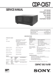
CDP-CX400/CX450
SERVICE MANUAL
US Model
Canadian Model
CDP-CX400/CX450
Ver 1.1 2001. 10
AEP Model
UK Model
E Model
Australian Model
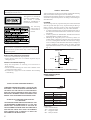
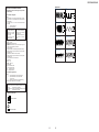
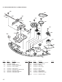
CDP-CX450
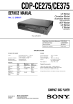
Photo; CDP-CX400
Model Name Using Similar Mechanism
NEW
CD Mechanism Type
CDM62-K1BD35A
Base Unit Type
BU-K1BD35A
Optical Pick-up Type
KSM-213BFN
SPECIFICATIONS
USA, Canadian
Europian
230 V AC, 50/60 Hz
COMPACT DISC PLAYER
9-929-232-12
Sony Corporation
2001J1600-1
© 2001.10
Home Audio Company
Published by Sony Engineering Corporation
Laser component in this product is capable of emitting radiation
exceeding the limit for Class 1.
This appliance is classified as
a CLASS 1 LASER product.
The CLASS 1 LASER
PRODUCT MARKING is
located on the rear exterior.
The following
caution label is
located inside of
the unit.
CAUTION
Use of controls or adjustments or performance of procedures
other than those specified herein may result in hazardous
radiation exposure.
Notes on chip component replacement
• Never reuse a disconnected chip component.
• Notice that the minus side of a tantalum capacitor may be
damaged by heat.
Flexible Circuit Board Repairing
• Keep the temperature of soldering iron around 270˚C
during repairing.
• Do not touch the soldering iron on the same conductor of the
circuit board (within 3 times).
• Be careful not to apply force on the conductor when soldering
or unsoldering.
SAFETY CHECK-OUT
After correcting the original service problem, perform the following
safety checks before releasing the set to the customer:
Check the antenna terminals, metal trim, “metallized” knobs, screws,
and all other exposed metal parts for AC leakage. Check leakage as
described below.
LEAKAGE
The AC leakage from any exposed metal part to earth Ground and
from all exposed metal parts to any exposed metal part having a
return to chassis, must not exceed 0.5 mA (500 microampers).
Leakage current can be measured by any one of three methods.
1. A commercial leakage tester, such as the Simpson 229 or RCA
WT-540A. Follow the manufacturers’ instructions to use these
instruments.
2. A battery-operated AC milliammeter. The Data Precision 245
digital multimeter is suitable for this job.
3. Measuring the voltage drop across a resistor by means of a
VOM or battery-operated AC voltmeter. The “limit” indication
is 0.75 V, so analog meters must have an accurate low-voltage
scale. The Simpson 250 and Sanwa SH-63Trd are examples of
a passive VOM that is suitable. Nearly all battery operated
digital multimeters that have a 2V AC range are suitable. (See
Fig. A)
To Exposed Metal
Parts on Set
0.15µF
1.5kΩ
Earth Ground
Fig. A. Using an AC voltmeter to check AC leakage.
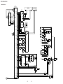
MODEL IDENTIFICATION
— BACK PANEL —
SAFETY-RELATED COMPONENT WARNING !!
COMPONENTS IDENTIFIED BY MARK ! OR DOTTED LINE
WITH MARK ! ON THE SCHEMATIC DIAGRAMS AND IN
THE PARTS LIST ARE CRITICAL TO SAFE OPERATION.
REPLACE THESE COMPONENTS WITH SONY PARTS
WHOSE PART NUMBERS APPEAR AS SHOWN IN THIS
MANUAL OR IN SUPPLEMENTS PUBLISHED BY SONY.
ATTENTION AU COMPOSANT AYANT RAPPORT
À LA SÉCURITÉ!!
LES COMPOSANTS IDENTIFIÉS PAR UNE MARQUE ! SUR
LES DIAGRAMMES SCHÉMATIQUES ET LA LISTE DES
PIÈCES SONT CRITIQUES POUR LA SÉCURITÉ DE
FONCTIONNEMENT. NE REMPLACER CES COMPOSANTS
QUE PAR DES PIÈCES SONY DONT LES NUMÉROS
SONT DONNÉS DANS CE MANUEL OU DANS LES
SUPPLÉMENTS PUBLIÉS PAR SONY.
2
AC
voltmeter
(0.75V)
PART NO.
PARTS No.
4-226-838-0π
4-226-838-1π
4-226-838-2π
4-226-838-3π
4-226-838-4π
4-226-838-5π
4-226-838-6π
MODEL
CX400 : US
CX400 : CND
CX450 : US
CX450 : CND
CX450 : AEP, UK
CX450 : AUS
CX450 : SP, MY
• Abbreviation
CND : Canadian model
AUS : Australian model
SP : Singapore model.
MY : Malaysia model.
SECTION 1
SERVICE NOTE
TABLE OF CONTENTS
1. SERVICING NOTE .......................................................... 3
2. GENERAL .......................................................................... 6
3. DISASSEMBLY
3-1.
3-2.
3-3.
3-4.
3-5.
3-6.
3-7.
3-8.
Upper Case Assembly ··················································· 7
Main Board Assembly ··················································· 7
Front Panel Assembly ···················································· 8
Table (400) Assembly ···················································· 8
Base (Door, Driving) Assembly ···································· 9
Pop-up Assembly ··························································· 9
Back Panel Assembly ·················································· 10
CDM Assembly ·························································· 10
4. SERVICE MODE ............................................................. 11
5. TEST MODE ..................................................................... 15
5-1. ADJ Mode ··································································· 15
5-2. Key and Display Check Mode ····································· 15
6. ADJUSTMENTS
6-1. Mechanical Adjustments ············································· 16
6-2. Electrical Adjustment ·················································· 18
NOTES ON HANDLING THE OPTICAL PICK-UP BLOCK
OR BASE UNIT
The laser diode in the optical pick-up block may suffer electrostatic
break-down because of the potential difference generated by the
charged electrostatic load, etc. on clothing and the human body.
During repair, pay attention to electrostatic break-down and also
use the procedure in the printed matter which is included in the
repain parts.
The flexible board is easily damaged and should be handled with
care.
NOTES ON LASER DIODE EMISSION CHECK
The laser beam on this model is concentrated so as to be focused on
the disc reflective surface by the objective lens in the optical pickup block. Therefore, when checking the laser diode emission,
observe from more than 30 cm away from the objective lens.
The emission check enables continuous checking of the S curve.
LASER DIODE AND FOCUS SEARCH OPERATION
CHECK
Carry out the “S curve check” in “CD section adjustment” and check
that the S curve waveform is output three times.
7. DIAGRAMS
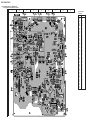
7-1. Circuit Boards Location ·············································· 20
7-2. Block Diagrams
• BD Section ································································ 21
• Main Section ····························································· 22
7-3. Schematic Diagram – BD Section – ···························· 24
7-4. Printed Wiring Board – BD Section – ························· 25
7-5. Printed Wiring Board – Main Section – ······················ 26
7-6. Schematic Diagram – Main (1/2) Section – ················ 27
7-7. Schematic Diagram – Main (2/2) Section – ················ 28
7-8. Printed Wiring Board – T. Sens Section – ··················· 29
7-9. Schematic Diagram – Sensor Section – ······················ 29
7-10. Schematic Diagram – Display Section – ···················· 30
7-11. Printed Wiring Board – Display Section – ·················· 31
7-12. Schematic Diagram – Jog Section – ··························· 32
7-13. Printed Wiring Board – Jog Section – ························ 33
7-14. Schematic Diagram – Power Section – ······················· 34
7-15. Printed Wiring Board – Power Section – ···················· 35
7-16. IC Block Diagrams ····················································· 36
7-17. IC Pin Functions ························································· 37
8. EXPLODED VIEWS
8-1.
8-2.
8-3.
8-4.
8-5.
8-6.
8-7.
Case Section ································································ 42
Chassis Section ···························································· 43
Front Panel Section ····················································· 44
Mechanism Section 1 (CDM54-K1BD35E) ··············· 45
Mechanism Section 2 (CDM54-K1BD35E) ··············· 46
Mechanism Section 3 (CDM54-K1BD35E) ··············· 47
Opeical Pick-up Section (KSM-213BFN/M-NP) ········ 48
9. ELECTRICAL PARTS LIST ........................................ 49
3
CD-TEXT TEST DISC
This unit is able to display the TEXT data (character information) written in the CD on its fluorescent indicator tube.
The CD-TEXT TEST DISC (TGCS-313:J-2501-126-A) is used for checking the display.
To check, perform the following procedure.
Checking Method:
1. Turn ON the power, set the disc on the disc table with the side labeled as “test disc” as the right side, close the front cover, and chuck the
disc.
2. The following will be displayed on the fluorescent indicator tube. (The display switches each time the TIME/TEXT button is pressed.)
Display : CD TEXT TEST DISC (Album Title)
3. Press the · button and play back the disc.
4. The following will be displayed on the fluorescent indicator tube. (If nothing is displayed, press the TIME/TEXT button.)
Display : 1kHz/0 dB/ L&R
5. Rotate ≠ and ± knob to switch the track. The text data of each track will be displayed.
For details of the displayed contents for each track, refer to “Table 1 : CD-TEXT TEST DISC Text Data Contents” and “Table 2 : CDTEXT TEST DISC Recorded Contents and Display”.
Restrictions in CD-TEXT Display
In this unit, some special characters will not be displayed properly. These will be displayed as a space or a character resembling it. For details,
refer to “Table 2 : CD-TEXT DISC Recorded Contents and Display”.
Table 1 : CD-TEXT TEST DISC Text Data Contents (TRACKS No. 1 to 41:Normal Characters)
TRACK
No.
Displayed Contents
TRACK
No.
Displayed Contents
1
1kHz/0dB/L&R
22
1kHz/-90dB/L&R
2
20Hz/0dB/L&R
23
Infinity Zero w/o emphasis//L&R
3
40Hz/0dB/L&R
24
Infinity Zero with emphasis//L&R
4
100Hz/0dB/L&R
25
400Hz+7kHz(4:1)/0dB/L&R
5
200Hz/0dB/L&R
26
400Hz+7kHz(4:1)/-10dB/L&R
6
500Hz/0dB/L&R
27
19kHz+20kHz(1:1)/0dB/L&R
7
1kHz/0dB/L&R
28
19kHz+20kHz(1:1)/-10dB/L&R
8
5kHz/0dB/L&R
29
100Hz/0dB/L*
9
7kHz/0dB/L&R
30
1kHz/0dB/L*
10
10kHz/0dB/L&R
31
10kHz/0dB/L*
11
16kHz/0dB/L&R
32
20kHz/0dB/L*
12
18kHz/0dB/L&R
33
100Hz/0dB/R*
13
20kHz/0dB/L&R
34
1kHz/0dB/R*
14
1kHz/0dB/L&R
35
10kHz/0dB/R*
15
1kHz/-1dB/L&R
36
20kHz/0dB/R*
16
1kHz/-3dB/L&R
37
100Hz Squer Wave//L&R
17
1kHz/-6dB/L&R
38
1kHz Squer Wave//L&R
18
1kHz/-10dB/L&R
39
1kHz w/emphasis/-0.37dB/L&R
19
1kHz/-20dB/L&R
40
5kHz w/emphasis/-4.53dB/L&R
20
1kHz/-60dB/L&R
41
16kHz w/emphasis/-9.04dB/L&R
21
1kHz/-80dB/L&R
NOTE : The contents of Track No. 1 to 41 are the same as those of the current TEST DISC-their titles are displayed.
4
Table 2: CD-TEXT TEST DISC Recorded Contents and Display
(In this unit, some special characters cannot be displayed. This is no a fault.)
TRACK
No.
Recorded contents
Display
42
! ” # $ %& ´
(21h to 27h)1kHz 0dB L&R
N All the same
43
( )
*+ , – . /
(28h to 2Fh)
N All the same
44
012345 67
(30h to 37h)
N All the same
45
89 : ; <=>?
(38h to 3Fh)
N All the same
46
@A B C D E F G
(40h to 47h)
N All the same
47
H I J K L MNO
(48h to 4Fh)
N All the same
48
P Q R S T U V W (50h to 57h)
N All the same
49
XYZ [ ¥ ] ^ _
(58h to 5Fh)
X Y Z [ \ ] ^ _ (58····
50
′
ab c de f g
(60h to 57h)
N All the same
51
h i j k l mn o
(68h to 6Fh)
N All the same
52
pq r s t u vw
(70h to 77h)
N All the same
53
x y z { I } ~
(78h to 7Fh)
x y z { I } ~
(78····
54
i ¢£¤¥ §
≥ C ª ¬ PR –
(A0h to A7h) 8859-1
i ¢£¤¥
(A0····
(A8h to AFh)
≥
55
′
µ¶ •
1
4
1
2
′
§
µ
is not displayed
(A8···· C ª ¬ PR– are not displayed
•
±
57
†
1
¿
(B8h to BFh)
†
58
À Á Â Ã Ä Å ÆÇ
(C0h to C7h)
N All the same
59
ÈÉÊË Ì Í Î Ï
(C8h to CFh)
N All the same
60
(D0h to D7h)
61
D ÑÒÓÔÕÖ
Ø Ù Ú Û Ü Y˙ ß
(D8h to DFh)
N All the same
˙ ß (D8····
ΦÙÚÛÜY
62
à á â ã ä åæç
(E0h to E7h)
N All the same
63
èéêë ì í î ï
(E8h to FFh)
N All the same
64
∂ ñòóôõ ö÷
(F0h to F7h)
o ñ ò ó ô õ ö ÷ (F0····
65
ø ù ú û ü y´
(F8h to FFh)
N All the same
66
No.66
N All the same
67
No.67
N All the same
56
to
99
2
º
to
No.99
3
3
4
ÿ
(B0h to B7h)
• (B0····
•
¿ (B8····
1
±
º
2
3
1
4
¶ are not displayed
1
2
3
4
are not displayed
to
N All the same
5
SECTION 2
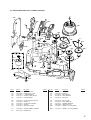
GENERAL
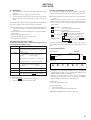
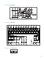
Front Panel
q;qaqs qd qf qg
9
45 6 7 8
qh
3
qj qk ql w;
2
1
r;
wa ws wd wf
wg
el
ekejehegef
ed es eae; wl
wk wjwh
Photo: CDP-CX400
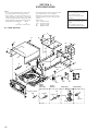
LOCATION OF PARTS AND CONTROLS
1
2
3
4
5
6
7
8
9
q;
qa
qs
qd
qf
qg
qh
qj
qk
ql
w;
6
1/u (power) button
STANDBY indicator
Display window
CONTINUE button
SHUFFLE button
PROGRAM button
REPEAT button
SCROLL button
Front cover
OPEN/CLOSE button
DISC EJECT button
EASY PLAY button and indicator
MENU/NO button
+100 button
YES button
DISC/CHARACTER/PUSH ENTER knob and button
CHECK button
CLEAR button
NAME SEARCH button
ARTIST MODE button and indicator
wa
ws
wd
wf
wg
wh
wj
wk
wl
e;
ea
es
ed
ef
eg
eh
ej
ek
el
r;
FADER button
X-FADE button
NO DELAY button
MEGA CONTROL button and indicator
≠ AMS ±/PUSH ENTER knob and button
p (stop) button
· (play) button and indicator
P (pause) button and indicator
HIT LIST button and indicator
GROUP 4 button and indicator
GROUP 3 button and indicator
GROUP 2 button and indicator
GROUP 1 button and indicator
GROUP FILE button
GROUP 8 button and indicator
GROUP 7 button and indicator
GROUP 6 button and indicator
GROUP 5 button and indicator
KEYBOARD jack
TIMER OFF/PLAY switch
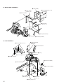
SECTION 3
DISASSEMBLY
Note : Follow the disassembly procedure in the numerical order given.
3-1. UPPER CASE
1 Three screws
(case 3 screw)
2 Two screws
@(case 3 screw)
3 Two screws
@(case 3 screw)
5 Upper Case
4 Two screws
@(case 3 screw)
3-2. MAIN BOARD
qa MAIN board
0 Four screws
(BVTP 3 × 8)
7 Flat type wire
(CN502)(15 core)
qs Flat type wire
(CN501)(23 core)
3 Connector (CN901)
1 Two screws (BVTP 3 × 8)
8 Two connectors
(CN505, CN506)
2 Bracket (R)
9 Three screws
(BVTP 3 × 8)
qd Two screws
(BVTP 3 × 8)
4 Three connectors
(CN503, CN801, CN903)
qf Blacket (L)
5 Connector (CNP902)
6 Connector (CNP504)
7
3-3. FRONT PANEL ASSEMBLY
1 Connector (CNP503)
2 Screw (BVTP 3 × 8)
5 Remove the claw
3 Two screws
(BVTP 3 × 8)
6 Remove the claw
7 Front panel assembly
4 Three screws
(BVTP 3 × 8)
3-4. TABLE (400) ASSEMBLY
3 Table (400) assembly
1 Screw (BVTP 3 × 16)
2 Guide (door)
4 Washer
8
3-5. BASE (DOOR DRI VING) ASSEMBLY
1 Two screws
(BVTP 3 × 8)
5 Cover (table)
4 Three screws (BVTP 3 × 8)
2 Cover (PT)
9 Base (door driveing)
assembly
6 Door assembly
3 Connector (CN602)
7 Two screws (BVTP 3 × 8)
8 Eight screws (BVTP 3 × 8)
3-6. POP-UP ASSEMBLY
2 Step screw
3 Pop-up assembly
1 Screw (PTPWH 3 × 6)
9
3-7. BACK PANEL ASSEMBLY
2 Cover (CDM)
1 Nine screws (BVTP 3 × 8)
3 Three screws
(BVTP 3 × 8)
4 Bracket (CDM)
6 Four screws
(BVTP 3 × 8)
7 Back panel assembly
5 Connector (CN991)
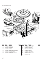
3-8. CDM ASSEMBLY
5 Magnet assembly
6 Washer
3 Six screws (BVTP 3 × 8)
8 CD mechanism
7 Spring
9 Washer
4 Bracket (top 400)
1 Connector (CN603)
qd CDM assembly
2 Connector (CN601)
0 Four screws
(BVTP 3 × 8)
qs Seven screws
(BVTP 3 × 8)
qa Screw (PSW 3 × 8)
10
SECTION 4
SERVICE MODE
SPECIAL FUNCTION
This unit is provided with several service modes.
Details are shown in the following table.
Turn on the power and press GROUP FILE , MEGA CONTROL and 1/u buttons.
Rotate the DISC/CHARACTER dial to enter any of the following modes.
Display
Mech Adjust
Table Roatation
All Lit Mode
Ship Mode
Normal Aging
Table Aging
Door Popup Aging
Color Bar (OSD)
Test Disp (OSD)
Memo Copy Mode
Model Name
Show Mcom Ver.
Demo
BUS Check
M kentou
Mechanism adjustment mode
Mode in which table keeps rotating
All lights ON mode
Default mode
Normal aging mode
Table aging mode
Door/popup aging mode
Color bar on OSD
TEST DISPLAY for OSD
Memo copy mode
Model name display
Software version display
400-memo writing mode
Bus check
Loading aging
To exit the mode, press 1/u button to enter the standby state.
(When selecting the Ship mode, the standby mode is automatically entered.)
AGING MODE
• Mode which repeatedly changes and plays back discs automatically in the unit.
• It will repeat aging as long as no errors occur.
• If an error occurs during aging, it will stop all servos, motors, etc.
instantaneously, display the error number, and stop operations.
However, the stopping conditions differ according to whether the
unit is equipped with the “self-protection function during errors”
described later.
The function serves to maintain the state of the unit when errors
occur.
Sequence of Aging Mode
1.
2.
3.
4.
5.
Order of Disc Change
(1 cycle takes 3 minutes)
$
Disc change
$
Load in
$
TOC read
$
Access of last track
$
3 second playback
6.
$
Access of first track
7.
$
3 second playback
8.
$
Load out
1.
$
No. 80
2.
$
No. 320
3.
$
No. 240
4.
$
No. 400
5.
$
No. 160
$
$
11
Special Aging Mode Functions
The aging mode is provided with the following convenient functions
• Disc setting mode (*1)
• Selection of presence of protection function during error (*2)
• Count function of aging cycle (*3)
*1 Disc setting mode:
5 discs are set before setting the aging mode. This mode makes
the setting of these discs more easy.
*2 Self protection function during errors:
Function which voluntarily corrects errors which occur during
normal operations by retries.
If this function is not provided, all operations will be stopped
without retiring. It is suitable for checking errors with low
reproducibility.
If this function is provided, and errors can be corrected by
retries, aging will be continued without stopping.
*3 Aging cycle count function:
Functions which displays the number of agings carried out on
the Fluorescent indicator tube in numbers. One aging cycle
consists of five discs.
Aging Procedure
1. Turn on the power and press the GROUP FILE , MEGA
CONTROL and 1/u buttons.
2. Rotate DISC/CHARACTER dial, select “Normal Aging” and
press the dial to start the aging mode.
3. When the disc set mode is set, the · and P LEDs blink.
4. Rotate the DISC/CHARACTER dial. The slits (No. 80, 160,
400, 240, 320) for setting the discs will come forward. Insert
the discs into these slits. Do not set the discs in other slits.
5. Set whether the self-protection function during errors is
equipped with the unit. Press the REPEAT button. If
“REPEAT” is displayed on the Fluorescent indicator tube, it
means the function is provided. If “REPEAT” is not displayed,
it means the function is not provided.
6. Press the · button.
7. The · LED blinks, the aging mode is set, and aging is started.
8. The aging cycle lasts 3 minutes. If errors occur during aging,
the error number will be displayed on the Fluorescent indicator
tube. (Refer to the following table for the details of the errors.)
9. Aging will be repeated as long as no errors occur.
10. After each aging cycle, the number displayed on the Fluorescent
indicator tube will increase.
11. To end aging, to end aging, press the 1/u button to enter the
standby mode.
Error code
Code number
Name
Contents
#Err 01
DISC sensor check 1
No disc in the specified slit
#Err 02
DISC sensor check 2
Disc in other slits
#Err 03
Table operation check 1
Table motor current over
#Err 04
Table operation check 2
No table sensor input
#Err 05
Loading operation check 1
Load in timeover
#Err 06
Loading operation check 2
Load out timeover
#Err 08
Table is not stopped within the specified time.
#Err 09
Stopped while both T.SENS 1 and 2 are “LOW”.
#Err *1
BU related check 1
Access timeover
#Err *2
BU related check 2
During high speed playback, COUNT timeout
#Err *3
BU related check 3
Q data read error
#Err *4
BU related check 4
]BU operation (from focus search to until signal can be read) timeover
#Err *5
BU related check 5
GFS monitor error
#Err *6
BU related check 6
Focus cannot be imposed by focus search
The * numbers mean the following according to the state of the unit during aging
2 : From chucking to end of TOC read
3 : From end of TOC read to end of last track playback
4 : From end of last track playback to end of first track playback
# : DISC No.
12
TABLE AGING MODE
• This mode is used for rotating the table randomly.
• Aging will be performed continuously unless an error occurs.
• When an error occurs, the error code will be displayed on the
fluorescent indicator tube.
Procedure:
1. Turn on the power and press the GROUP FILE , MEGA
CONTROL and 1/u buttons.
Rotate the DISC/CHARACTER dial, select “Table Aging”
and press the dial.
Rotate the DISC/CHARACTER dial and set the disk in the
slit whose number is being displayed (150, 149, 300, 1, 2)
2. When the mode is set, both the · and P indicators will
start to blink.
3. When the · button is pressed, only the · indicator will
blink and aging starts.
4. To end the mode, press the 1/u button or disconnect the
power cord from the outlet.
During aging, operations will be carried out sequentially in the order
of No. 1, No. 2, No. 150, No. 149, and No. 300 slits.
The error codes displayed during operations and when errors occur
are the same as the “AGING MODE” described earlier.
DOOR POP UP AGING MODE
• This mode is used for performing aging of the CD pop up part
and door open/close.
It is used for checking if operations are performed normally.
Method:
1. Turn on the power and press the GROUP FILE , MEGA
CONTROL and 1/u buttons.
Rotate the DISC/CHARACTER dial, select “Door Popup
Aging” and press the dial.
2. Aging starts, and door open/close and up/down operations of
the pop up part are performed continuously.
3. To end the mode, press the 1/u button.
TABLE ROTATION MODE
• This mode is used for electrical adjustments. Refer to the section
on Electrical Adjustments.
$
COMMAND MODE: CD3
$
The error codes displayed during operations and when errors occur
are the same as the “AGING MODE” described earlier.
This unit
(Copy source)
$
Procedure:
1. Set a disc in the DISC 1 slit.
2. Turn on the power and press the GROUP FILE , MEGA
CONTROL and 1/u buttons.
Rotate the DISC/CHARACTER dial, select “Table Roatation”
and press the dial.
3. When the mode is set, both the · and P indicators will
start to blink.
4. When the · button is pressed, only the · indicator will
blink and aging starts.
5. To end the mode, press the 1/u button or disconnect the
power cord from the outlet.
TITLE MEMO SHIFT MODE
• This mode is used for writing title memo information recorded in
this unit in a different unit.
Use it for transferring disc memo contents written by the customer to the new units when replacing the unit, etc.
Connection:
Flow of data
$
LOADING AGING MODE
• This mode is used for repeating loading operations continuously.
• Aging will be performed continuously unless an error occurs.
• When an error occurs, the error code will be displayed on the
fluorescent indicator tube.
Another unit
(Copy destination)
COMMAND MODE: CD1
CONTROL A1 II connection cord provided
CONTROL A1 II
Procedure:
1. Connect two units using the CONTROL A1 II connection
cord shown in the figure.
2. Set the COMMAND MODE switch of the copy source unit to
CD3 and the COMMAND MODE switch of the copy
destination unit to CD1 .
3. With the power on, while pressing the GROUP 7 button and
§ OPEN/CLOSE button of the copy destination unit, press
the +100 button.
4. When the data has been transferred, the fluorescent indicator
tube displays “complete” for about 1 second.
MODEL NAME DISPLAY
•
Model names can be displayed on the fluorescent indicator tube
for checking the microprocessor model setting, etc.
Procedure:
With the power ON, while pressing the GROUP FILE and MEGA
CONTROL buttons, press the 1/u button.
Rotate the DISC/CHARACTER dial, select “Model Name”
and press the dial.
The model name is displayed on the fluorescent indicator tube.
Let the model name be displayed for three seconds and exit the
mode.
MICROPROCESSOR VERSION DISPLAY
•
The microprocessor version can be displayed on the fluorescent
indicator tube.
Procedure:
With the power ON, while pressing the GROUP FILE and MEGA
CONTROL buttons, press the 1/u button.
Rotate the DISC/CHARACTER dial, select “Show Mcom Ver.”
and press the dial.
The microprocessor version is displayed on the fluorescent indicator
tube.
Let the model name be displayed for three seconds and exit the
mode.
ALL LIT MODE
•
This mode is used for lighting the whole fluorescent indicator
tubes and LEDs.
Procedure:
With the power ON, while pressing the GROUP FILE and MEGA
CONTROL buttons, press the 1/u button.
Rotate the DISC/CHARACTER dial, select “All Lit Mode” and
press the dial.
Both the fluorescent indicator tubes and LEDs will light up
completely.
To end this mode, press the 1/u mode.
13
MECHANISM ADJUSTMENT MODE
•
This mode is used for mechanism adjustments. Refer to the
section on Mechanism Adjustments.
SHIPMENT MODE
•
This mode is used for setting the unit to the shipment state.
Do not execute it without a proper reason as it erases the
memory of the title memo recorded by the customer.
Procedure:
Set the TIMER switch to OFF . Next, with the power ON, while
pressing the GROUP FILE button and MEGA CONTROL button,
press the 1/u button. If the switch state is normal, the model name
will be displayed on the fluorescent indicator tube and the unit will
set into the shipment mode.
If the various switches are not set to their designated positions, error
will be displayed on the fluorescent indicator tube.
TITLE MEMO RECORDING CHECK MODE
This mode is not required for servicing. Do not execute without a
proper reason.
If executed, the memory of the title memo recorded by the customer
will be erased.
14
SECTION 5
TEST MODE
5-1. ADJ Mode
5-2. Key and Display Check Mode
1.
To set this mode, connect the test point (AFADJ) on the MAIN
board to Ground, and connect the power supply plug to the outlet.
2.
3.
Turn ON the power of the unit, set disc to disc table, and perform
chucking.
Disconnect the power supply plug from the outlet.
To set ADJ mode, connect the test point (ADJ) of the MAIN
board to Ground, and connect the power supply plug to the
outlet.
In this mode, table rotation and loading operations are not performed
because it is taken that the disc has already been chucked.
Note: The same operations are also performed in the following when
the test point (ADJ) is connected to Ground after turning on
the power.
• Direct search (movement of sledding motor) is not performed during accessing
• Ignored even when GFS becomes L
• Ignored even when the Q data cannot be read
• Focus gain does not decrease
ADJ Mode Special Functions Table
(The buttons shown with ( ) function by using the supplied remote commander only)
Button
Function
CONTINUE
Servo average display
Displays VC, FE, RF, TE and traverse in hexadecimal
numbers
SHUFFLE
PROGRAM
Focus bias display
Each time this is pressed, the focus bias is
switched
between 1 and 2
(1)
Bias actually set Optimum bias Minimum jitter
(2)
+:Upper aliasing bias -:Lower aliasing bias
Auto gain display
Displays focus, tracking, sledding in
hexadecimal
numbers
GROUP 3 (3)
Turns off the tracking and sledding servo
GROUP 8 (8)
Turns on the tracking and sledding servo
CHECK
S-JI mode.
(Exits this mode when the 1/u button is pressed.)
To end the ADJ mode
1. Press the 1/u button and disconnect the plug.
2. Remove the wire between ADJ and GND.
Note: When this mode is executed, all title memos recorded will be
erased.
• When this button is pressed, “line # No. #” will be displayed.
However, these will not be displayed for the following special
buttons. However, these will not be displayed for the following
special buttons.
p (stop) button: FL segment check
(Refer to FL Tube Check Patterns)
P (pause) button: FL grid check
(Refer to FL Tube Check Patterns)
The P LED also lights up simultaneously.
· (play) button: All FL segment and grid will light up.
· LED also lights up simultaneously.
TIMER switch:
When the switch position is PLAY , the
STANDBY LED lights up. It goes OFF
when set to OFF .
Each time this button is pressed, the value of the “Got ## keys”
increases. Buttons pressed once will not be counted when pressed
again.
FL Tube Check Patterns
Magnified
Segment check
Grid check
A
B
C
D
E
F
G
• When the jog dial and AMS is rotated to the right, the GROUP
LEDs light up in the order of 1n2..8nHIT LISTnEASY PLAY
ARTIST MODE nMEGA CONTROLn1.
• When the jog dial and AMS is rotated to the left, the GROUP
LEDs light up in the order of 8n7..1 nMEGA CONTROL
ARTIST MODE nEASY PLAYnHIT LISTn8.
• Abbreviation
FL: Fluorescent Indicator Tube
To end the ADJ mode
1. Disconnect the plug.
2. Remove the wire between AFADJ and GND.
Adjustment Location: MIAN board (See page 26)
15
SECTION 6
ADJUSTMENTS
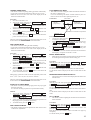
6-1. MechaniCAL Adjustments
Pop Up Mechanism Adjustment
1. Turn on the power and set the dick to number 24.
2. With the power ON, while pressing the GROUP FILE and
MEGA CONTROL buttons, press the 1/u button to enter
the Adjastment mode.
3. Rotate the JOG dial and select the mechanism adjustment mode.
(“Mech Adjust” is displayed.)
Press the JOG dial.
4. Keep pressing the GROUP 1 button to operate the loading
mechanism, and continue pressing until the disc table locks.
(Fig-1)
5. Keep pressing the GROUP 2 button to raise the pop up part.
6. Loosen the adjusting screw, move the screwdriver left and right
until the lever (POP UP) does not touch the slit wall, and secure
the screw. (Fig-2)
At this position,this
part will be locked.
FIg-1
The following buttons have special functions in this mode.
GROUP 1
GROUP 5
GROUP 2
GROUP 6
button: Loading mechanism IN operation
button: Loading mechanism OUT operation
button: Pop up part UP operation
button: Pop up part DOWN operation
Cover (chassis 400)
Lever (POP-UP 400)
Fix to the center so that the
lever (POP-UP 400) does
not touch the slit.
FIg-2
16
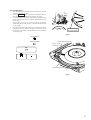
Sensor Adjustment
1. Enter the adjustment mode and select “Mech Adjust” with the
JOG dial, and press the dial.
2. Press the GROUP 1 button to operate the loading mechanism,
and continue pressing until the disc table locks. (Fig-3)
3. Loosen the fixing screw and move the holder so that both PLAY
button LED (green) and the ARTIST MODE button LED
(green) light.
If the holder is not in the correct position, the MEGA
CONTROL button LED (orange) or the PAUSE button LED
(orange) lights.
4. Moving the disc table right and left with a hand after the screw
is fixed, the table will move by the play of a disc table. If the
LEDs light up alternately, the adjustment will be performed
correctly. (Fig-4)
At this position,this
part will be locked.
FIg-3
ARTIST MODE
MEGA CONTROL
Holder (table sensor 400)
S tight, screw
(PTTWH 3 × 6)
Table (400) assembly
Swing
FIg-4
17
6-2. ELECTRICAL ADJUSTMENT
Note: A clear RF signal waveform means that the shape “◊” can be
clearly distinguished at the center of the waveform.
Note:
1. CD Block is basically designed to operate without adjustment.
Therefore, check each item in order given.
2. Use YEDS-18 disc (3-702-101-01) unless otherwise indicated.
3. Use an oscilloscope with more than 10MΩ impedance.
4. Clean the object lens by an applicator with neutral detergent
when the signal level is low than specified value with the
following checks.
S-Curve Check
RF signal waveform
VOLT/DIV : 200mV
TIME/DIV : 500ns
+0.25
level : 1.2 –0.20
Vp-p
Adjustment Location: BD board (See page 19)
Oscilloscope
E-F Balance Check
BD board
Oscilloscope
TP (FE1)
TP (VC)
BD board
Procedure :
1. Chuck the disc (YEDS-18) beforehand, and disconnect the
power cord from the outlet.
2. Connect oscilloscope to test point TP (FE1) on BD board.
3. Connect test point (ADJ) on MAIN board to ground with lead
wire.
4. The ADJ mode is set when the power cord is inserted into the
outlet and power is supplied.
5. The fifth track is played automatically.
6. Press the CHECK button.
7. Check the oscilloscope waveform (S-curve) is symmetrical
between A and B. And confirm peak to peak level within 3±1
Vp-p.
S-curve waveform
Symmetry
A
TP (TE)
TP (VC)
Procedure :
1. Chuck the disc (YEDS-18) beforehand, and disconnect the
power cord from the outlet.
2. Connect oscilloscpe to test point TP (TE) on BD board.
3. Connect test point (ADJ) on MAIN board to ground with lead
wire.
4. The ADJ mode is set when the power cord is inserted into the
outlet and power is supplied.
5. The fifth track is played automatically.
6. Press the GROUP 3 button. (The tracking servo and the
sledding servo are turned OFF.)
7. Check the level B of the oscilliscope's waveform and the A
(DC voltage) of the center of the Traverse waveform.
Confirm the following :
A/B x 100 = less than ± 22%
Within 3 ± 1 Vp-p
Traverse waveform
B
Center of the waveform
Pressing the 1/u button stops the output of the waveform (s
curve).
9. After check, remove the lead wire connected in step 3.
Note : • Try to measure several times to make sure than the ratio of
A : B or B : A is more than 10 : 7.
• Take sweep time as long as possible and light up the
brightness to obtain best waveform.
B
8.
A (DC voltage)
0V
Level : 1.3 ± 0.6 Vp-p
8.
Adjustment Location: BD board (See page 19)
Press the GROUP 8 button. (The tracking servo and sledding
servo are turned ON.) Confirm the C (DC voltage) is almost
equal to the A (DC voltage) is step 7.
RF Level Check
Traverse waveform
Oscilloscope
BD board
TP (RF)
TP (VC)
Procedure :
1. Connect oscilloscope to test point TP (RF) on BD board.
2. Turn Power switch on.
3. Put disc (YEDS-18) in to play the number five track.
4. Confirm that oscilloscope waveform is clear and check RF
signal level is correct or not.
C (DC
voltage)
0V
Tracking servo
Sledding servo
OFF
9.
Tracking servo
Sledding servo
ON
Disconnect the lead wire of TP1 (ADJ) connected in step 2.
Adjustment Location: BD board (See page 19)
18
Disc Sensor Adjustment
Be sure to perform this adjustment after sensor adjustment in
MECHANICAL ADJUSTMENT.
5.
Connection:
MAIN board
TP1
D.S
GND
T.P
Oscilloscope
6.
D.S: Pin 1
T.P: Pin 3
Rotate the DISC/CHARACTER knob in the counterclockwise
direction and the disc table starts to rotate in the same direction.
Check that the waveform at this time is the same as that in step
4. If larger by a considerable extent, rotate the DISC/
CHARACTER knob in the clockwise direction and the disc
table starts to rotate in the same direction. Repeat from step 4.
Rotate RV501 of the MAIN board and adjust so that the H and
L portions of the D.S waveform become the same.
CH1
CH2
Waveform:
CH1
D.S
D.S
CH1
Adjust so that these widths
become the same.
Adjustment Location
CH2
1.
2.
3.
4.
T.P
Connect the oscilloscope to Pins 1, 2, and 3 of TP1 of the
MAIN board.
Check that no discs are loaded in the unit.
With the power ON, while pressing the GROUP FILE and
MEGA CONTROL buttons, press the 1/u button. Rotate
the DISC/CHARACTER dial, select “Table Rotation” and
press the dial.
The disc table starts to rotate in the clockwise direction.
Loosen the fixing screw, move the mounting board (SENSOR),
and secure the mounting board (SENSOR) at the point the H
portion of the T.P waveform comes the center of the H portion
of the D.S waveform.
[ BD BOARD ] – Side B –
TP
(FE1)
IC102
TP
TP (RF)
(TE)
IC103
D. sens (out) board
TP
(VC)
S tight, screw
(PTTWH 3 × 6)
CH1
D.S
CH2
T.P
Should be at the center
19
SECTION 7
DIAGRAMS
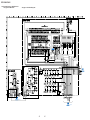
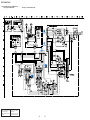
7-1. CIRCUIT BOARDS LOCATION
LED board
MAIN board
D. SENS (IN) board
DISPLAY board
TRANS board
D. SENS
(OUT) board
KEY board
T. SENS board
D. MOTOR board
DOOR SW board
JOG board
BD board
LOADING SW board
L. T. MOTOR board
LOCK SW board
20
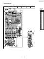
CDP-CX400/CX450
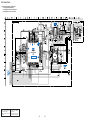
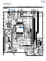
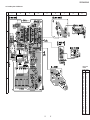
7-2. BLOCK DIAGRAMS
– BD SECTION –
OPTICAL PICK-UP
BLOCK
(KSM-213BFN)
IC101
DIGITAL SERVO
DIGITAL SIGNAL PROC.
D/A CONV.
IC103
RF AMP
VC
+5V
A
B
C
5 A
RFO 16
51 RFAC
6 B
RFI 17
43 RFDC
E
F
8 D
FE 14
39 FE
11 E
TE 13
41 TE
10 F
LD
DRIVE
2ND
CD IN
7
R OUT 75
IC401
AMP
8
2
IC302
LPF
1
6
IC302
AMP
MUTE
Q324
7
LINE
OUT
MUTE
Q322,323
R-CH
DOWN S612
UP DOOR
40 SE
Q101
LD
DIGITAL
OUT
OPTICAL
L OUT 72
7 C
D
J903
IC901
DIGITAL
OUT
D OUT 60
12 VC
LMUTE 80
LD ON 22
3 LD
MUTE CONT
Q325,327-329
14 XLON
OPEN S611
CLOSE POP UP
GND
IC501(1/2)
SYSTEM CONTROL
HOLD SW 21
PD
F+
17 CH1RO
F-
16 CH1FO
CH1RI 19
CH1FI 20
4
DATA 5
IC102
MOTOR/COIL DRIVE
FOCUS
COIL
S621
LOADING
29 SMUTE
4 PD
VR
32 FFDR
33 FRDR
IC507
DOOR SW 89
1
31 DATA
IC507
10
13
CLOK 7
S622
LOCK
33 CLK
XLAT 6
27 XLT
SQCK 2
37 SQCK
LD SW 92
SCLK 9
T+
TRACKING
COIL
1 CH2RO
T-
30 TFDR
2 CH2FO
CH2FI 5
31 TRDR
13 CH3RO
CH3RI 10
29 SRDR
12 CH3FO
CH3FI 9
28 SFDR
27 CH4RO
CH4INS 24
26 MDP
16
M102
SLED
MOTOR
CH2RI 4
SCOR 20
20 SCOR
SQSO 1
36 SUBQ
SENS 8
38 SENS
LOAD IN 7
S101
LIMIT
IN SW
SSTP 27
MOTOR
8
6
LOAD OUT 6
7
DOOR OUT 11
3
DOOR in 10
4
XTAI 66
26 CH4FO
2
+5V
X101
16.9344MHz
MUTE 15
M LOADING
MOTOR
DRIVE
M
M101
SPINDLE M
MOTOR
M602
IC961
XTAO 67
M603
DOOR
MOTOR
M
M601
TABLE
MOTOR
Q552
TBLL 26
IC941
MOTOR
SWITCH
Q941,942
+5V
XRST 3
M
2
4
MOTOR
DRIVE
Q562
TBLR 28
MOTOR
SWITCH
Q951,952
25 LPH
30 IC RESET
• RCH is omitted
• Signal Path
8
6
IC81-84
TSENS1 77
: CD
TABLE
SENSOR
TSENS2 74
: DIGITAL OUT
Q81,D81
DISC
SENSOR
DSENS 91
RV501
IC802
SDC
DSDLT 48
TRE 41
26 CS
R OUT 19
23 TRE
25 SIN
G OUT 18
24 SCLK
5 RESET
IC804
SYNC GEN
X801
14.3118MHz
US CND MODEL
14.1875MHz
AEP,AUS,MY
SP,UK MODEL
6 CLKI
HDO 29
B OUT 20
11 HSYNC
I OUT 17
8
IC805
12
6
14
13
7
11
9
4
16
2
18
IC803
VIDEO AMP
2 R IN
J801
VIDEO
OUT
CV 20
3 G IN
4 B IN
8 DOCKI
7 CLKO
X861
22 FSCI
17.734475MHz
AEP,AUS,MY
SP,UK MODEL
23 FSCO
Q861
17 COMP
13 VSYNC
10 SYNC
BLKO 32
14 DISP
6 SC
FLD 8
11 EVEN
VDO 30
SYNC 31
SC 24
X450 MODEL
RESET
21
21
A
CDP-CX400/CX450
– MAIN SECTION –
IC501(2/2)
SYSTEM CONTROL
FL701
FLUORESCENT
INDICATOR TUBE
86
88
. D0
85 D7
81
IC504
SRAM
10
11
13
. D0
15 D7
19
67
3.
25
65
.
63
.
61
.
26
.
1
IC701
FL DRIVER
FL DATA 1
63 DA
FL CLK 2
62 SCK
71
49 CE
WE 27
46 WE
OE 22
44 OE
50
60 RESET
F1
F2
Q701
DIG16 55
SEG01 5
SEG35 39
AD1(36) 4
Q521
CE 20
F2
DIG1 49
.
DIG15 54
61 CS
FL T1 97
F1
40
68
. A0
58
. A14
60
. 72
.
56
. 59
57
A0 23
.
A14 21
.
2.
FL702
FLUORESCENT
INDICATOR TUBE
IC702
FL DRIVER
D701-712,715
S714(1/2),S721(1/2)
4 DATA
LED 11
7 RST DRIVER 24
8 CLK
6 LT
LED LATCH 80
T911
F1
+5V
FL701
Q576
STBY LED 93
IC704
FL DRIVER
13 OSC1
X501
10MHz
15 OSC2
13 SIN
SEG0 43
15 CLK
SEG14 29
D913
FL702
F2
VFL
D JOG1 43
D JOG2 50
S701-706
DISC/
CHARACTER
KEY
MATRIX
IC910
DVDD
S711-715
T JOG1 40
T JOG2 39
KEY 94
-20V REG
Q941
11 AD0
KEY
MATRIX
S721-726
AMS
KEY
MATRIX
3
S741-745
KEY
MATRIX
IC920
3
+5V
3
S751-755
6 AD5
IC502
KEY CONTROL
8 SIRCS IN SIRCS OUT 33
5 CE
CE 54
Q850
CARRIER OUT 2
12
RECT
+5V
REG
1
10
11
9
4
14 RESET
5
2
RST 53
1
3
+5V
REG
1
CX450 MODEL
+5V
13
D931-934
1
IC980
CX450
+5V
SIRCS 52
+7V
REG
IC921
7 AD4
KEY
MATRIX
RECT
AU VEE
+7V
KEY
MATRIX
D921-924
1
AU VCC
9 AD2
S761-768
+5V
REG
aVDD
10 AD1
RE702
8
Q591-593
LED
DRIVE
M +B
D591-594
D596,597
M -B
T901
6
IC930
MUTE
+5V
3
3
+5V
REG
2
IC503
2WAY DRIVE
D901-904
L991
RECT
LINE
FILTER
D905,906
RECT
Q581
15 X IN
X580
7.28MHz
RECT
F1
14 SOUT
RE701
D911
-30V REG
Q911
VFL
5 RESET
DATA IN 100
F2
CA1 OUT 11
16 XOUT
CA1 IN 12
CX450 MODEL
BUS IN 5
J901
BUS OUT 4
Q950
CONTROL 1
J902
IC931
2
RESET 12
A
4
Q901
AC IN 18
16
RESET
RELAY
DRIVE
RELAY 24
RESET
22
22
RY991
AC
IN
CDP-CX400/CX450
Waveforms
THIS NOTE IS COMMON FOR PRINTED WIRING
BOARDS AND SCHEMATIC DIAGRAMS.
(In addition to this, the necessary note is printed
in each block.)
5 IC101 wh MDP
1 IC101 yj XTAI
Note:
• All capacitors are in µF unless otherwise noted. pF: µµF
50 WV or less are not indicated except for electrolytics
and tantalums.
• All resistors are in Ω and 1/4 W or less unless otherwise
specified.
¢
•
: internal component.
• C : panel designation.
Note:
The components identified by mark ! or dotted
line with mark ! are critical for safety.
Replace only with part
number specified.
•
•
•
•
•
•
•
•
•
6 IC502 qh XOUT
2 IC101 ta RF AC
1.2Vp-p
Note:
Les composants identifiés par
une marque ! sont critiques
pour la sécurité.
Ne les remplacer que par une
piéce por tant le numéro
spécifié.
7.28MHz
4.6Vp-p
(PLAY)
3 IC101 ra TE
7 IC501 qg OSC2
2.5V
10MHz
APPROX 500mVp-p (PLAY)
4 IC101 el FE
4.2Vp-p
8 IC804 7 CLKO
2.5V
APPROX 200m Vp-p (PLAY)
For printed wiring boards.
Note:
• X : parts extracted from the component side.
• Y : parts extracted from the conductor side.
®
•
: Through hole.
• b : Pattern from the side which enables seeing.
(The other layers' patterns are not indicated.)
Parts on the pattern face side seen from the
pattern face are indicated.
Parts on the parts face side seen from the
parts face are indicated.
• Indication of transistor
C
Q
7.5µsec
16.9MHz
U : B+ Line.
V : B– Line.
H : adjustment for repair.
Voltages and waveforms are dc with respect to ground
under no-signal (detuned) conditions.
no mark : STOP
Voltages are taken with a VOM (Input impedance 10 MΩ).
Voltage variations may be noted due to normal production tolerances.
Waveforms are taken with a oscilloscope.
Voltage variations may be noted due to normal production tolerances.
Circled numbers refer to waveforms.
Signal path.
J : CD
c : digital out
Abbreviation
CND : Canadian model
AUS : Australian model
SP : Singapore model.
MY : Malaysia model.
Caution:
Pattern face side:
(Side B)
Parts face side:
(Side A)
2.4Vp-p
3.1Vp-p
For schematic diagrams.
These are omitted
B E
BC E
These are omitted
23
23
14MHz
4.2Vp-p
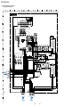
CDP-CX400/CX450
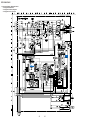
7-3. Schematic Diagram – BD Section –
• See page 23 for Waveforms.
• See page 36 for IC Block Diagrams.
• See page 38 for IC Pin Functions.
KSM-213BFN
PIN FUNCTION
TO
MAIN BOARD
(Page 27)
16
The components identified by
mark 0 or dotted line with mark
0 are critical for safety.
Replace only with part number
specified.
Les composants identifiés par
une marque 0 sont critiques
pour la sécurité.
Ne les remplacer que par une
pièce portant le numéro spécifié.
24
24
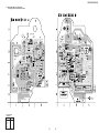
CDP-CX400/CX450
7-4. Printed Wiring Board – BD Section –
• See page 20 for Circuit Boards Location.
KSM-213BFN
16
16
• Semiconductor
Location
Ref. No.
Location
IC101
IC102
IC103
C-5
B-2
C-4
Q101
C-3
25
25
TO
MAIN BOARD
(Page 26)
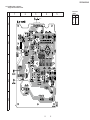
CDP-CX400/CX450
7-5. Printed Wiring Board – MAIN Section –
• See page 20 for Circuit Boards Location.
1
2
3
4
5
6
7
8
9
• Semiconductor
(Page 35)
(Page 35)
(Page 35)
(Page 29)
Location
(Page 31)
Ref. No.
A
B
C
(Page 33)
D
(Page 31)
TP
(ADJ)
TP
(AFADJ)
E
(Page 33)
F
(Page 25)
G
H
(Page 29)
26
26
Location
D327
D329
D501
D521
D580
D941
D942
D-4
D-3
D-7
G-7
H-7
C-8
C-8
IC302
IC401
IC402
IC501
IC501
IC502
IC503
IC504
IC507
IC802
IC803
IC804
IC805
IC901
IC910
IC920
IC921
IC930
IC931
IC980
E-3
F-3
E-3
F-6
F-6
H-6
H-7
G-8
G-5
C-4
C-2
C-5
C-3
E-1
G-3
E-2
B-3
A-4
D-6
A-2
Q322
Q323
Q324
Q325
Q327
Q328
Q329
Q422
Q423
Q424
Q425
Q521
Q552
Q562
Q570
Q571
Q572
Q576
Q580
Q581
Q861
Q941
Q950
E-2
E-2
D-2
D-4
D-3
D-3
D-3
D-2
D-2
D-2
D-3
G-8
E-6
E-6
B-7
B-7
H-8
E-7
G-6
G-7
C-5
B-8
B-1
CDP-CX400/CX450
Ver 1.1 2001.10
7-6. Schematic Diagram – MAIN (1/2) Section –
• See page 23 for Waveforms.
• See page 36, 37 for IC Block Diagrams.
(Page 30)
(Page 29)
(Page 32)
(Page 30)
(Page 24)
(Page 29)
PIN FUNCTION
CX400 : M30620MC-407FP
CX450 : M30622MGA-309FP
7
6
(Page 34)
(Page 34)
(Page 32)
(Page 34)
27
27
CDP-CX400/CX450
7-7. Schematic Diagram – MAIN (2/2) Section –
• See page 23 for Waveforms.
• See page 36 for IC Block Diagrams.
• See page 40 for IC Pin Functions.
8
28
28
CDP-CX400/CX450
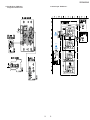
7-8. Printed Wiring Board – SENSOR Section –
• See page 20 for Circuit Boards Location.
7-9. Schematic Diagram – SENSOR Section –
TO
MAIN BOARD
(Page 26)
(Page 27)
(Page 27)
(Page 26)
29
29
CDP-CX400/CX450
7-10. Schematic Diagram – DISPLAY Section –
• See page 23 for Waveforms.
• See page 37 for IC Block Diagrams.
(Page 32)
(Page 27)
(Page 27)
30
30
CDP-CX400/CX450
7-11. Printed Wiring Board – DISPLAY Section –
• See page 20 for Circuit Boards Location.
1
2
3
(Page 33)
(Page 26)
4
5
6
7
• Semiconductor
Location
Ref. No.
A
B
C
CX450 : AEP,UK,SP
MY,AUS
(Page 26)
D
E
31
31
Location
D591
D592
D593
D594
D595
D596
D597
D598
D701
D702
D703
D704
D705
D706
D707
D708
D709
D710
E-1
E-3
E-1
E-2
E-2
E-1
E-2
E-3
D-3
D-2
D-2
D-1
D-1
D-3
D-2
D-2
D-1
C-4
IC701
IC702
IC703
B-2
C-1
A-1
Q591
Q592
Q593
Q701
E-1
E-2
E-3
C-2
CDP-CX400/CX450
7-12. Schematic Diagram – JOG Section –
• See page 23 for Waveforms.
(Page 30)
(Page 27)
(Page 27)
32
32
CDP-CX400/CX450
7-13. Printed Wiring Board – JOG Section –
• See page 20 for Circuit Boards Location.
• Semiconductor
1
2
3
4
5
(Page 31)
A
CX450 : AEP,UK,SP,
MY,AUS
B
C
(Page 26)
D
(Page 26)
E
33
33
Location
Ref. No.
Location
D711
D712
D715
D-4
E-5
A-4
IC704
B-4
CDP-CX400/CX450
7-14. Schematic Diagram – POWER Section –
• See page 23 for Waveforms.
• See page 37 for IC Block Diagrams.
(Page 27)
(Page 27)
(Page 27)
The components identified by
mark 0 or dotted line with mark
0 are critical for safety.
Replace only with part number
specified.
Les composants identifiés par
une marque 0 sont critiques
pour la sécurité.
Ne les remplacer que par une
pièce portant le numéro spécifié.
34
34
CDP-CX400/CX450
7-15. Printed Wiring Board – POWER Section –
1
2
3
4
5
6
7
8
9
(Page 26)
A
B
(Page 26)
C
(Page 26)
• Semiconductor
Location
D
Ref. No.
E
35
35
Location
D901
D902
D903
D904
D905
D906
D907
D911
D912
D913
D921
D922
D923
D924
D931
D932
D933
D934
D935
D991
B-2
B-2
B-2
B-2
B-2
B-2
B-2
E-3
E-4
D-4
D-3
D-3
E-3
E-3
D-3
D-3
D-4
D-4
C-3
C-3
IC941
IC961
B-2
B-3
Q901
Q911
Q931
Q941
Q942
Q951
Q952
B-3
E-4
C-3
A-4
A-4
A-4
A-4
CDP-CX400/CX450
IC103 CXA2568M-T6 (BD BOARD)
7-16. IC BLOCK DIAGRAMS
IC931 BA3993F (MAIN BOARD)
RFAC
BIAS
ASYI
ASYO
AVDD0
IGEN
AVSS0
ADIO
RFDC
CE
TE
52
51 50 49 48
47
46 45
44
43 42 41
23 LC/PD
22 LD_ON
VEE
HOLD 1
VEE
OPERATIONAL
AMPLIFIER
ANALOG SWITCH
PD
TRACKING
SERVO
TRACKING
PWM GENERATOR
SLED
SERVO
SLED PWM
GENERATOR
33
32
31
30
29
28
FRDR
FFDR
TRDR
TFDR
SRDR
SFDR
DIGITAL
CLV
26 MDP
25 LOCK
MIRR, DFCT,
FOK
DETECTOR
24 FOK
23 DFCT
22 MIRR
5
B
6
C
7
D
8
VEE
9
VEE
RF SUMMING AMP
VC
15 RFE
SERIAL IN
INTERFACE
ERROR AMP
FOCUS
VC
VEE
14 FE
VC
F 10
E 11
13 TE
VC
VC 12
TRACKING
ERROR AMP
VC
VCC
VC
VEE
VC
24
23
22
21
20
19
18
17
IC804 CXD1159Q (MAIN BOARD)
CPU
INTERFACE
9 10 11 12 13 14 15 16 17 18 19 20
DATA
XLAT
CLOK
SENS
SCLK
VDD
ATSK
WNDE 25
C2PO
SCOR
5 6 7 8
WFCK
XUGF
XPCK
GFS
4
SPOA
SPOB
XLON
3
XRST
21 COUT
SYSM
SQSO
SQCK
1 2
1
VC
VC BUFFER
SERVO AUTO
SEQUENCER
4
18 RFTC
17 RF_1
16 RFO
RF_EQ_AMP
VC
COMP
RMUT 79
LMUT 80
FOCUS PWM
GENERATOR
SERVO
INTERFACE
OVER SAMPLING
DIGITAL FILTER
AIN2 76
FOCUS
SERVO
27 SSTP
3rd ORDER
NOISE SHAPER
AOUT2 77
AVDD2 78
PWM GENERATOR
37 XTSL
36 TES1
35 TEST
34 VSS
A
VC
VDD2
LOUT2 75
SUBCODE
PROCESSOR
PWM
3
TSD
19 RF_BOT
AIN
PWM
4
AOUT
LOUT1 72
2
21 HOLD_SW
20 AGCCONT
(50%/30%
OFF)
VCC
GND
CLOCK
GENERATOR
SERVO DSP
AVSS1 73
AVSS2 74
3
VSS2
TIMING
LOGIC
5
FSC1
XVDD 65
66
67
68
69
70
71
6
Band Gap
EMPH 64
XTAI
XTAO
XVSS
AVDD1
AOUT1
AIN1
LD
A/D
CONVERTER
BCK 63
7
APC LD AMP
VC
EFM
DEMODULATOR
8
VREF
FSC0
PCMD 62
D/A
INTERFACE
ASYMMETRY
CORRECTION
DIGITAL
PLL
16K
RAM
AGCVTH 2
SC
LRCK 61
INTERNAL BUS
DIGITAL
OUT
ERROR
CORRECTOR
40 SE
39 FE
38 VC
GND
AVSS3
56 55 54 53
CT
PCO
FILI
FILO
CLTV
59 58 57
VCC
GND
VDD
VSS
AVDD3
60
24 VCC
VCC
APC PD AMP
POFF
DOUT
IC101 CXD2587Q (BD BOARD)
1/4
WND 26
16 PSEL
IC102 BA6392FP-E2 (BD BOARD)
PHASE
COMPARATOR
1/227
1/5
TEST 27
15 VINT
28 GND
F
BUFF
BUFF
CAPA IN 1 3
14 MODE
27 CH4 OUT F
LEVEL
SHIFT
R
VDD1 28
26 CH4 OUT R
1/4
BUFF
CH1 R IN 4
CH1 F IN 5
R
F
SLB-CARRIER
CONTROL
CH1 OUT R 2
BUFF
25 VB IN
INTERFACE
HD0 29
24 VS IN
1/6 or 7
1/65
1/525 or 625
H-DECODER
V-DECODER
12 VSS1
BUFF
23 VB IN
VREF OUT 7
GND 8
CH2 F IN 9
CH2 R IN 10
21 VCC
F
R
CAPA IN 2 11
CH2 OUT R 12
CH2 OUT F 13
VD0 30
22 VCC
F
INTERFACE
INTERFACE
R
BUFF
F
V-CONTROL
20 CH3 F IN
SYNC 31
OUTPUT CONTROL
19 CH3 R IN
18 CAPA IN 3
F
BUFF
BUFF
R
R
BUFF
11 LALT
TEST
GENERATOR
VREF IN 6
13 SCOF
RESET
GENERATOR
CH1 OUT F 1
10 NC
9 NC
BLKO 32
17 CH3 OUT R
16 CH3 OUT F
MUTE
36
36
1
2
3
4
5
6
7
8
HR
VR
LR
EXT
CLK1
CLK0
FLD
15 MUTE
BFO
GND 14
GND2
ROUT
GOUT
BOUT
CVOUT
VCC2
NC
YTRAP
YOUT
COUT
NC
NC
IC803 CXA2075M (MAIN BOARD)
24
23
22
21
20
19
18
17
16
15
14
13
VIDEO
OUT
SYNC
ADO
MATRIX
R-Y
Modulator
LPF
B-Y
Modulator
REGULATOR
9
10
11
12
VCC1
8
BFOUT
SCIN
NC
BIN
7
PULBE
GEN
NC
6
5
NPIN
4
GIN
RIN
GND1
PHASE
SHIFTER
SIN-PULBE
3
BPF
LPF
CLAMP
2
75
DRIVER
INTERNAL
TRAP
DELAY
1
75
DRIVER
SYNCIN
B-OUT
Y/C MIX
NC
G-OUT
R-OUT
TRAP
SWITCH
QC
QD
QE
QF
QG
QH
QI
QJ
QK
QL
QM
QN
IC702 M66310FP (DISP BOARD)
24
23
22
21
20
19
18
17
16
15
14
13
0
D
1
D
CK
CK
0
R
D
R
D
R
D
1
CK
CK
0
R
D
R
D
1
CK
CK
0
R
D
R
D
1
CK
CK
0
R
D
R
D
1
CK
CK
0
R
D
R
D
1
CK
CK
0
R
D
R
D
1
CK
CK
0
R
D
R
D
1
CK
CK
0
R
D
R
D
1
CK
CK
0
R
D
R
D
1
CK
CK
0
R
D
R
D
1
D
D
R
D
0
4
5
6
7
8
9
10
11
12
QP
3
CK
QO
0
1
SQP
2
R
D
GND
1
CK
R
1
CLK
0
CK
D
RST
D
1
R
LT
R
QB
CK
QA
0
R
D
OE
D
1
CK
CK
0
R
DATA
1
CK
VCC
D
CK
CK
CK
CK
CK
R
R
R
R
IC941, IC961 LA6510 (TRANS BOARD)
–
–
+
+
VSENCE2
VCC
+VIN1
VEE
+VIN2
–VIN2
VOUT2
VSENCE1
VOUT1
–VIN1
1 2 3 4 5 6 7 8 9 10
37
7-17. IC PIN FUNCTIONS
• IC101 DIGITAL SIGNAL PROCESSOR (CXD2587Q) (BD board)
Pin No.
1
SQSO
Pin Name
I/O
O
2
SQCK
I
Clock input for SQSO read-out
3
XRST
I
System reset “L” : reset
4
SYSM
I
Muting input “H” : mute
5
DATA
I
Serial data input, supplied from CPU
6
XLAT
I
Latch input, supplied from CPU
7
CLOK
I
Serial data transfer clock input, supplied from CPU
8
SENS
O
SENS signal output to CPU
9
SCLK
I
SENS serial data read-out clock input
10
VDD
—
Digital power supply
11
ATSK
I/O
Input pin for anti-shock (Connected to ground)
12
SPOA
I
Microcomputer escape interface input A
13
SPOB
I
Microcomputer escape interface input B
14
XLON
O
Microcomputer escape interface output
15
WFCK
O
WFCK output (Not used)
16
XUGF
O
Not used
17
XPCK
O
Not used
18
GFS
O
Not used
19
C2PO
O
Not used
20
SCOR
O
Sub-code sync output
21
COUT
I/O
Numbers of track counted signal input/output (Not used)
22
MIRR
I/O
Mirror signal input/output (Not used)
23
DFCT
I/O
Defect signal input/output (Not used)
24
FOK
I/O
Focus OK input/output (Not used)
25
LOCK
I/O
GFS is sampled by 460 Hz. H when GFS is H (Not used)
26
MDP
O
Output to control spindle motor servo
27
SSTP
I
Input signal to detect disc inner most track
28
SFDR
O
Sled drive output
29
SRDR
O
Sled drive output
30
TFDR
O
Tracking drive output
31
TRDR
O
Tracking drive output
32
FFDR
O
Focus drive output
33
FRDR
O
Focus drive output
34
VSS
—
Digital ground
35
TEST
I
TEST pin connected normally to ground
36
TES1
I
TEST pin connected normally to ground
37
XTSL
I
X'tal selection input (Connected to ground)
38
VC
I
Center voltage input pin
39
FE
I
Focus error signal input
40
SE
I
Sled error signal input
• Abbreviation
GFS : Guarded Frame Sync
38
Function
Sub-Q 80-bit and PCM peak level data output (CD text data output)
Pin No.
41
TE
I/O
I
Tracking error signal input
42
CE
I
Center servo analog input
43
RFDC
I
RF signal input
44
ADIO
O
Test pin (Not used)
45
AVSS0
—
Analog ground
46
IGEN
Pin Name
I
Function
Stabilized current input for operational amplifiers
AVDD0
—
Analog power supply
ASYO
O
EFM full swing output
49
ASYI
I
Asymmetry comparate voltage input
50
BIAS
I
Asymmetry circuit constant current input
51
RFAC
I
EFM signal input
52
AVSS3
—
53
CLTV
I
Control voltage input for master VCO1
54
FILO
O
Filter output for master PLL
55
FILI
I
Filter input for master PLL
56
PCO
O
Charge-pump output for master PLL
57
47
48
Analog ground
AVDD3
—
Analog power supply
58
VSS
—
Digital ground
59
VDD
—
Digital power supply
60
DOUT
O
Digital-out output pin
61
LRCK
O
D/A interface LR clock output (ƒ = Fs) (Not used)
62
PCMD
O
D/A interface serial data output (Not used)
63
BCK
O
D/A interface bit clock output (Not used)
64
EMPH
O
Playback disc output in emphasis mode (Not used)
65
XVDD
—
Power supply for master clock
66
XTAI
I
X'tal oscillator circuit input (16.9344MHz)
67
XTAO
O
X'tal oscillator circuit output (16.9344MHz)
68
XVSS
—
Ground for master clock
69
AVDD1
—
Analog power supply
70
AOUT1
O
L-ch analog output
71
AIN1
I
L-ch operational amplifiers input
72
LOUT1
O
L-ch line output
73
AVSS1
—
74
AVSS2
—
75
LOUT2
O
R-ch line output
76
AIN2
I
R-ch operational amplifiers input
77
Analog ground
AOUT2
O
R-ch analog output
78
AVDD2
—
Analog power supply
79
RMUT
O
R-ch “0” detection flag output
80
LMUT
O
L-ch “0” detection flag output
• Abbreviation
EFM : Eight to Fourteen Modulation
PLL : Phase Locked Loop
39
Ver 1.1 2001.10
• IC501 SYSTEM CONTROL (M30620MC-407FP) (CX400) (MAIN board)
• IC501 SYSTEM CONTROL (M30622MGA-309FP) (CX450) (MAIN board)
Pin No.
1
40
Pin Name
FLDATA
I/O
O
Function
Data output to fluorescent indicator driver
2
FLCLK
O
Clock output to fluorescent indicator driver
3
RM_IN
I
SIRCS input
4
BUSOUT
O
Ctrl-A1 output
5
BUSIN
I
Ctrl-A1 input
6
LODOUT
O
Loading motor OUT direction signal
7
LODIN
O
Loading motor IN direction signal
8
GND
—
Data bus width selection input
9
GND
—
Chip operation mode selection
10
P_DOOR_OUT
O
Door motor "open" direction
11
P_DOOR_IN
O
Door motor "close" direction
12
RESET
I
Reset input
13
10MHz
I
Oscillator output
14
GND
15
10MHz
—
I
—
Power supply input
External oscillator is connected to this input.
16
Vcc
17
PULL-UP
I
Power supply input
Non-maskable interrupt port. Pulled-up.
18
ACIN
I
AC input
19
KBCIN
I
Keyboard clock input
20
SCOR
I
CXD2587 synchronous signal input
21
KBDOUT
O
Keyboard data output
22
KBDIN
I
Keyboard data input
23
KBCOUT
O
Keyboard clock output
24
ICSW
O
Terminal to supply power to peripheral ICs
25
LPH
O
CXD2587 LPH output
26
TBLR
O
Table motor clockwise direction
27
XLT
O
CXD2587 XLY output
28
TBLL
O
Table motor counterclockwise direction
29
SMUTE
O
2nd audio input, mute output
30
ICRESET
O
Peripheral IC reset output
31
DATA
O
CXD2587/OSD/DF data output
32
OPEN
—
Use is prohibited.Not used
33
CLK
O
CXD2587/OSD/DF clock output
34
AMUTE
O
CXD2587 mute output
35
OPEN
—
Not used.
36
SUBQ
I
Q data input port
37
SQCK
O
Q data read clock output
38
SENS
I
Sense input from CXD2587
39
TJOGB
I
AMS JOG input
40
TJOGA
I
AMS JOG input
41
TRE
I
OSD busy input (CX450)
42
SEL_ES
I
HiFi/ES select input
43
JOGA
I
Disc JOG input
44
OE
O
SRAM output enable
45
OPEN
—
Not used.
46
WE
O
SRAM write enable
47
PRGLT
O
Not used.
48
OSDLT
O
OSD latch output (CX450)
49
CS
O
SRAM CS output
Pin No.
50
JOGB
I/O
O
51
LED
O
Interal illumination LED output
52
TOSHIBA_SIRCS
O
Bidirectional microprocessor 455 kHz output enable output (CX450)
53
TOSHIBA_RST
O
Bidirectional microprocessor reset output (C450)
54
TOSHIBA/CE
O
Bidirectional microprocessor bidirectional function ON/OFF(CX450)
55
OPEN
—
Not used.
56
A14
O
57
A13
O
58
A12
O
59
A11
O
60
A10
O
61
A9
O
62
Vcc
—
63
A8
O
64
Vcc
—
65
A7
O
66
A6
O
67
A5
O
68
A4
O
69
A3
O
70
A2
O
71
A1
O
72
A0
O
73
NTSC
I
74
TSENS4
I
75
TSENS2
I
76
TSENS3
I
77
TSENS1
I
78
DSOUT
I
Disc sensor read result output
79
HHOUT
O
OR output of TSENS1/2
80
LEDLT
O
LED driver latch output
81
D7
I
82
D6
I
83
D5
I
84
D4
I
85
D3
I
86
D2
I
87
D1
I
88
D0
I
89
DOORSW
I
Door switch input (A/D)
90
SELECT
I
Selector (ADJ/AFADJ)
91
DSENS
I
Disc sensor input (A/D)
92
LOADINGSW
I
Loading switch input (A/D)
93
STNBY_L
O
Standby LED output
94
KEY
I
Key input (A/D)
95
FLT2
O
Fluorescent indicator driver (M35500) latch output
96
Avss
—
Analog power supply input
97
FLT
O
Fluorescent indicator driver (MSM9202) latch output
98
Vref
I
Standard voltage input
99
Avss
I
Analog power supply input
100
FLDATA_I
Pin Name
—
Function
Disc JOG input
SRAM address output
Power supply terminal
SRAM address output
OSD NTSC output (CX450)
Table sensor input
SRAM data
Data input from fluorescent indicator driver (M35500)
41
SECTION 8
EXPLODED VIEWS
NOTE:
• -XX, -X mean standardized parts, so they may
have some difference from the original one.
• Items marked “*” are not stocked since they are
seldom required for routine service. Some delay
should be anticipated when ordering these items.
• Color Indication of Appearance Parts Example:
KNOB, BALANCE (WHITE) . . . . (RED)
Â
Â
Parts color Cabinets color
The components identified by
mark 0 or dotted line with mark
0 are critical for safety.
Replace only with part number
specified.
• The mechanical parts with no reference number
in the exploded views are not supplied.
• Hardware (# mark) list and accessories and
packing materials are given in the last of this
parts list.
• Abbreviation
CND : Canadian model
AUS : Australian model
SP
: Singapore model.
MY : Malaysia model.
Les composants identifiés par une
marque 0 sont critiques pour la
sécurité.
Ne les remplacer que par une
piéce portant le numéro spécifié.
8-1. CASE SECTION
7
#1
#1
5
3
3
#1
8
#1
6
3
#1
#1
#1
2
#1
#1
#1
10
1
4
not supplied
#1
#1
3
#1
not supplied
not supplied
14
#1
13
#1
CX450
9
T901
T911
CX400
CX450
(US, CND)
CX450
(SP, MY)
CX450 (UK)
CX450 (AUS)
11
FRONT PANEL
12
11
CNP901
CNP901
CNP901
#1
CNP901
11
42
Ref. No.
1
2
3
4
5
6
6
6
7
8
9
9
9
10
10
10
Part No.
Description
Remark
4-226-841-01
4-226-855-11
4-210-291-01
1-500-386-11
COVER(PT)
UPPER CASE
SCREW(CASE 3 TP2)
FILTER, CLAMP (FERRITE CORE)
(CX450:US,CND)
1-792-466-11 WIRE(FLAT TYPE) (23 CORE)
A-4725-033-A MAIN BOARD, COMPLETE (CX450:US,CND)
A-4725-038-A MAIN BOARD, COMPLETE
(CX450:AEP,UK,SP,MY,AUS)
A-4725-053-A MAIN BOARD, COMPLETE (CX400)
4-985-553-11 CUSHION
4-226-876-01 COVER(CDM)
A-4725-034-A TRANS BOARD, COMPLETE (CX450:AUS)
A-4725-039-A TRANS BOARD, COMPLETE
(CX450:AEP,UK,SP,MY)
A-4725-051-A TRANS BOARD, COMPLETE (CX400/
CX450:US,CND)
4-226-838-01 PANEL, BACK (CX400:US)
4-226-838-11 PANEL, BACK (CX400:CND)
4-226-838-21 PANEL, BACK (CX450:US)
Ref. No.
10
10
10
10
11
11
* 12
14
0 CNP901
Part No.
Description
Remark
4-226-838-31
4-226-838-41
4-226-838-51
4-226-838-61
PANEL, BACK (CX450:CND)
PANEL, BACK (CX450:AEP,UK)
PANEL, BACK (CX450:AUS)
PANEL, BACK (CX450:SP,MY)
1-569-008-21
1-770-019-11
3-703-244-00
3-703-249-01
1-696-845-11
ADAPTOR, CONVERSION (CX450:SP,MY)
ADAPTOR, CONVERSION PLUG 3P (CX450:UK)
BUSHING (2104), CORD
SCREW, S TIGHT, +PTTWH 3X6
CORD, POWER (CX450:AUS)
0 CNP901 1-777-071-31 CORD, POWER (CX450:AEP,UK,SP,MY)
0 CNP901 1-783-531-41 CORD, POWER (CX400/CX450:US,CND)
0 T901
1-433-666-11 TRANSFORMER, POWER (CX400/
CX450:US,CND)
0 T901
1-433-668-11 TRANSFORMER, POWER
(CX450:AEP,UK,SP,MY)
0 T901
1-433-877-11 TRANSFORMER, POWER (CX450:AUS)
0 T911
0 T911
1-435-327-11 TRANSFORMER, POWER (CX400/
CX450:US,CND)
1-435-328-11 TRANSFORMER, POWER
(CX450:AEP,UK,SP,MY,AUS)
43
8-2. CHASSIS SECTION
#1
55
56
65
#2
54
#1
#4
not supplied
#1
#1
57
66
59 60
57
57
not supplied
#1
#7
53
61
#7
#5
64
67
63
62
#5
#5
68
58
not supplied
not supplied
CDM62-K1BD35A
SECTION-2
69
CDM62-K1BD35A
SECTION-1
CDM62-K1BD35A
SECTION-3
52
69
#4
#1
#1
51
#1
70
#7
#1
71
Ref. No.
Part No.
Description
51
52
53
54
55
X-4952-641-1
3-356-601-11
4-226-834-01
4-226-833-01
1-676-840-11
DOOR ASSY
SCREW, STEP
COVER (TABLE)
GUIDE (DOOR)
LED BOARD
56
57
58
59
60
4-215-968-01
3-703-249-01
1-676-834-11
1-676-828-11
4-225-873-01
WINDOW (INTERNAL ILLUMINATION)
SCREW, S TIGHT, +PTTWH 3X6
D.SENS (OUT) BOARD
T.SENS BOARD
HOLDER (TABLE SENSOR 400)
Remark
Ref. No.
Part No.
Description
61
62
63
64
65
1-676-833-11
4-216-096-01
4-216-089-01
3-701-447-21
X-4952-500-1
D.SENS (IN) BOARD
SCREW (T1), STEP
SHAFT (CENTER)
WASHER, 10
TABLE (400) ASSY
66
67
68
* 69
70
4-216-088-02
4-216-093-01
4-216-092-02
3-378-400-01
4-965-822-12
GUIDE (DISC)
ROLLER
HOLDER (ROLLER)
CUSHION, SARANET
FOOT
71
44
4-931-169-01 FOOT
Remark
8-3. FRONT PANEL SECTION
110
109
115
FL701
110
107
CX450
108
114
110
110
106
111
112
110
110
106
FL702
105
110
110
113
102
CX450
(AEP, UK,
SP, MY, AUS)
not
supplied
101
104
103
Ref. No.
101
101
101
Part No.
Description
Remark
103
X-4952-636-1 PANEL ASSY, FRONT (CX400)
X-4952-637-1 PANEL ASSY, FRONT (CX450:US,CND)
X-4952-638-1 PANEL ASSY, FRONT
(CX450:AEP,UK,SP,MY,AUS)
4-219-323-01 RING (DIA. 50-CX300)
(CX450:AEP,UK,SP,MY,AUS)
4-226-847-01 KNOB (AMS)
104
105
106
107
108
4-226-846-01
X-4952-642-1
4-985-553-21
3-917-216-21
1-792-465-11
109
A-4725-031-A DISP BOARD, COMPLETE (CX450:US,CND)
102
Ref. No.
109
109
110
111
112
112
KNOB (DISC)
BRACKET (CASE) ASSY
CUSHION
KNOB (TIMER)
WIRE (FLAT TYPE) (15 CORE)
112
114
* 115
FL701
FL702
Part No.
Description
Remark
A-4725-036-A DISP BOARD, COMPLETE
(CX450:AEP,UK,SP,MY,AUS)
A-4725-049-A DISP BOARD, COMPLETE (CX400)
4-951-620-01 SCREW (2.6X8), +BVTP
1-676-832-11 KEY BOARD
A-4725-030-A JOG BOARD, COMPLETE (CX450:US,CND)
A-4725-035-A JOG BOARD, COMPLETE
(CX450:AEP,UK,SP,MY,AUS)
A-4725-048-A JOG BOARD, COMPLETE (CX400)
4-215-969-01 HOLDER (LED.RM) (CX450)
4-929-709-31 GUIDE (FL TUBE)
1-517-959-11 INDICATOR TUBE, FLUORESCENT
1-517-960-11 INDICATOR TUBE, FLUORESCENT
45
8-4. MECHANISM SECTION 1 (CDM62-K1BD35A)
158
162
#6
157
159
161
163
154
154
163
157
164
165
#6
160
156
154
170
154
166
153
152
168
155
167
M603
152
169
154
151
Ref. No.
Part No.
Description
Part No.
Description
151
152
153
154
155
4-226-827-01
4-216-093-01
4-216-100-01
4-933-134-11
4-226-832-01
BASE (DOOR DRIVING)
ROLLER
HOLDER (POP-UP)
SCREW (+PTPWH M2.6X8)
LEVER (PU JOINT)
161
162
163
164
165
4-216-104-01
4-219-326-01
3-701-441-21
4-226-828-01
4-226-829-01
SPRING (POP-UP), TENSION
BELT (DIA. 42X1.2)
WASHER
GEAR (CAM)
GEAR (PULLEY)
156
157
158
159
160
4-216-099-01
4-216-103-01
4-998-716-01
4-216-102-01
4-228-352-01
SLIDER (POP-UP)
SPRING (POP-UP), COMPRESSION
SCREW, BU FITTING
SHAFT (POP-UP FULCRUM)
LEVER (POP-UP 400)
166
167
168
169
170
4-226-831-01
4-226-830-01
1-676-838-11
1-676-839-11
4-951-620-01
GEAR (B)
GEAR (A)
DOOR SW BOARD
D.MOTOR BOARD
SCREW (2.6X8), +BVTP
M603
1-541-632-11 MOTOR, DC (DOOR)
46
Remark
Ref. No.
Remark
8-5. MECHANISM SECTION 2 (CDM62-K1BD35A)
#7
211
213
221
#1
214
215
210
209
#3
207
217
#3
217
208
216
218
212
215
202
218
not supplied
220
219
202
M601,
M602
206
205
206
201
203
Ref. No.
not supplied
204
Part No.
Description
201
202
203
204
205
A-4672-895-A
4-951-620-01
1-676-837-11
4-933-134-11
1-676-835-11
MOTOR (400) ASSY
SCREW (2.6X8), +BVTP
L.T.MOTOR BOARD
SCREW (+PTPWH M2.6X8)
LOCK SW BOARD
206
207
208
209
210
X-4952-503-1
3-701-446-21
4-216-081-01
3-701-441-21
4-998-716-01
211
212
Remark
Ref. No.
Part No.
Description
213
214
215
216
217
4-225-865-01
A-4672-676-B
4-216-058-01
4-216-057-01
4-225-876-01
SLIDER (400)
CAMASSY
GEAR (CENTER)
GEAR (CENTER 2)
BELT (400)
LEVER (FULCRUM 400) ASSY
WASHER, 8
SPRING (MG), TORSION
WASHER
SCREW, BU FITTING
218
219
220
221
M601
4-225-870-01
4-225-869-01
1-676-836-11
X-4950-901-5
1-541-309-11
PULLEY (400)
GEAR (TABLE 400)
LOADING SW BOARD
HOLDER ASSY, BU
MOTOR, L (RF-370C)(TABLE)
4-216-082-01 HOLDER (MAGNET), TORSION
A-4672-768-A MAGNET ASSY
M602
1-541-309-11 MOTOR, L (RF-370C)(LOADING)
Remark
47
8-6. MECHANISM SECTION 3 (CDM62-K1BD35A)
267
265
270
266
269
270
271
270
268
263
#6
259
270
272
260
269
262
261
258
251
257
264
256
260
259
255
#6
252
254
251
253
Ref. No.
Part No.
Description
251
252
253
254
255
3-325-697-21
4-216-078-01
4-216-079-02
4-216-080-01
X-4950-900-1
WASHER
LEVER (LOADING)
LIMITTER (LEVER)
SPRING (LIMITTER), TORSION
BRACKET (LEVER) ASSY
256
257
258
259
260
4-225-871-01
4-216-077-01
4-216-076-01
4-216-067-01
3-701-441-21
HOLDER (F400)
SPRING (HOLDER FR), TORSION
HOLDER (R)
SPRING (CLAMP), COMPRESSION
WASHER
261
4-225-868-01 SHAFT (CLAMP 400)
Remark
Ref. No.
Part No.
Description
262
263
264
265
266
X-4952-502-1
X-4952-501-1
X-4952-499-1
X-4950-901-5
4-216-085-01
HOLDER (DISC R400) ASSY
HOLDER (DISC L400) ASSY
LEVER (LOCK 400) ASSY
HOLDER ASSY, BU
SPRING (F-1), TENSION
267
0 268
269
* 270
271
4-216-086-01
8-820-026-03
4-957-577-01
4-992-054-01
1-769-069-11
SPRING (F-2), TENSION
OPTICAL PICK-UP BLOCK KSM-213BFN
SCREW PTP WH (2.6X8) (DIA. 10)
RUBBER, VIBRATION PROOF
WIRE (FLAT TYPE) (16 CORE)
* 272
A-4724-761-A BD BOARD, COMPLETE
The components identified by
mark 0 or dotted line with mark
0 are critical for safety.
Replace only with part number
specified.
48
Remark
Les composants identifiés par
une marque 0 sont critiques
pour la sécurité.
Ne les remplacer que par une
pièce portant le numéro spécifié.
SECTION 9
ELECTRICAL PARTS LIST
BD
Note:
The components identified by
mark ! or dotted line with mark
! are critical for safety.
Replace only with part number
specified.
Les composants identifiés par une
marque ! sont critiques pour la
sécurité.
Ne les remplacer que par une
piéce portant le numéro spécifié.
When indicating parts by reference
number, please include the board
name.
• Due to standardization, replacements in the parts
list may be different from the parts specified in the
diagrams or the components used on the set.
• -XX, -X mean standardized parts, so they may
have some difference from the original one.
• Items marked “*” are not stocked since they are
seldom required for routine service. Some delay
should be anticipated when ordering these items.
• RESISTORS
All resistors are in ohms
METAL: Metal-film resistor
METAL OXIDE: Metal Oxide-film resistor
F : nonflammable
Ref. No.
Part No.
Description
Remark
*
A-4724-761-A BD BOARD, COMPLETE
*******************
<CAPACITOR>
Ref. No.
• SEMICONDUCTORS
In each case, u: µ , for example:
uA...: µ A..., uPA...: µ PA..., uPB...: µ PB...,
uPC...: µ PC..., uPD...: µ PD...
• CAPACITORS
uF : µ F
• COILS
uH : µ H
• Abbreviation
CND : Canadian model
AUS : Australian model
SP
: Singapore model.
MY : Malaysia model.
Part No.
Description
Remark
C159
C161
C162
C163
C164
1-163-019-00
1-126-205-11
1-126-205-11
1-126-205-11
1-163-038-91
CERAMIC CHIP
ELECT CHIP
ELECT CHIP
ELECT CHIP
CERAMIC CHIP
0.0068uF
47uF
47uF
47uF
0.1uF
10%
20%
20%
20%
50V
6.3V
6.3V
6.3V
25V
C101
C102
C103
C104
C106
1-163-005-11
1-163-038-91
1-163-005-11
1-163-021-91
1-164-346-11
CERAMIC CHIP
CERAMIC CHIP
CERAMIC CHIP
CERAMIC CHIP
CERAMIC CHIP
470PF
0.1uF
470PF
0.01uF
1uF
10%
50V
25V
10%
50V
10.00% 50V
16V
C165
C166
C167
C168
C171
1-163-038-91
1-163-038-91
1-163-235-11
1-163-237-11
1-163-137-00
CERAMIC CHIP
CERAMIC CHIP
CERAMIC CHIP
CERAMIC CHIP
CERAMIC CHIP
0.1uF
0.1uF
22PF
27PF
680PF
25V
25V
5.00% 50V
5.00% 50V
5%
50V
C107
C108
C109
C110
C111
1-164-346-11
1-163-035-00
1-163-145-00
1-163-017-00
1-163-251-11
CERAMIC CHIP
CERAMIC CHIP
CERAMIC CHIP
CERAMIC CHIP
CERAMIC CHIP
1uF
0.047uF
0.0015uF
0.0047uF
100PF
16V
50V
5%
50V
5%
50V
5.00% 50V
C172
C181
C182
1-163-251-11 CERAMIC CHIP
1-163-137-00 CERAMIC CHIP
1-163-251-11 CERAMIC CHIP
100PF
680PF
100PF
5.00% 50V
5%
50V
5.00% 50V
C112
C113
C114
C115
C116
1-163-038-91
1-163-038-91
1-163-038-91
1-126-607-11
1-126-607-11
CERAMIC CHIP
CERAMIC CHIP
CERAMIC CHIP
ELECT CHIP
ELECT CHIP
0.1uF
0.1uF
0.1uF
47uF
47uF
20%
20%
C117
C118
C119
C120
C121
1-126-209-11
1-163-275-11
1-163-231-11
1-163-038-91
1-163-038-91
ELECT CHIP
CERAMIC CHIP
CERAMIC CHIP
CERAMIC CHIP
CERAMIC CHIP
100uF
0.001uF
15PF
0.1uF
0.1uF
20.00% 4V
5.00% 50V
5.00% 50V
25V
25V
C122
C123
C124
C125
C126
1-135-214-21
1-163-021-91
1-164-005-11
1-163-038-91
1-163-038-91
TANTAL. CHIP
CERAMIC CHIP
CERAMIC CHIP
CERAMIC CHIP
CERAMIC CHIP
4.7uF
0.01uF
0.47uF
0.1uF
0.1uF
20.00% 10V
10.00% 50V
25V
25V
25V
C127
C130
C131
C140
C141
1-109-982-11
1-164-004-11
1-135-216-11
1-163-038-91
1-163-038-91
CERAMIC CHIP
CERAMIC CHIP
TANTALUM CHIP
CERAMIC CHIP
CERAMIC CHIP
1uF
0.1uF
10uF
0.1uF
0.1uF
10.00% 10V
10%
25V
20%
10V
25V
25V
C151
C153
C154
C156
C157
1-163-237-11
1-163-038-91
1-164-336-11
1-163-237-11
1-163-145-00
CERAMIC CHIP
CERAMIC CHIP
CERAMIC CHIP
CERAMIC CHIP
CERAMIC CHIP
27PF
5.00% 50V
0.1uF
25V
0.33uF
25V
27PF
5.00% 50V
0.0015uF 5%
50V
25V
25V
25V
4V
4V
<CONNECTOR>
CN101
CN102
1-770-072-11 CONNECTOR,(LIF(NON-ZIF))FFC23P
1-777-937-11 CONNECTOR, FFC/FPC 16P
<IC>
IC101
IC102
IC103
8-752-386-85 IC CXD2587Q
8-759-455-91 IC BA6392FP-E2
8-752-085-51 IC CXA2568M-T6
<COIL>
L101
L102
1-414-234-22 INDUCTOR CHIP 0uH
1-414-234-22 INDUCTOR CHIP 0uH
<TRANSISTOR>
Q101
8-729-010-08 TRANSISTOR
MSB710-RT1
<RESISTOR>
R101
R102
R103
R104
R105
1-216-077-91
1-216-097-91
1-216-077-91
1-216-085-00
1-216-097-91
RES-CHIP
RES-CHIP
RES-CHIP
METAL CHIP
RES-CHIP
15K
100K
15K
33K
100K
5%
5%
5%
5%
5%
1/10W
1/10W
1/10W
1/10W
1/10W
R106
R107
R108
R109
R110
1-216-061-00
1-216-061-00
1-216-073-00
1-216-121-91
1-216-025-91
METAL CHIP
METAL CHIP
METAL CHIP
RES-CHIP
RES-CHIP
3.3K
3.3K
10K
1M
100
5%
5%
5%
5%
5%
1/10W
1/10W
1/10W
1/10W
1/10W
49
BD
Ref. No.
DISP
Part No.
Description
R111
R113
R116
R117
R119
1-216-121-91
1-216-121-91
1-216-025-91
1-216-049-91
1-216-043-91
RES-CHIP
RES-CHIP
RES-CHIP
RES-CHIP
RES-CHIP
1M
1M
100
1K
560
5%
5%
5%
5%
5%
Remarks
1/10W
1/10W
1/10W
1/10W
1/10W
R123
R124
R131
R135
R136
1-216-073-00
1-216-097-91
1-216-037-00
1-216-295-91
1-216-295-91
METAL CHIP
RES-CHIP
METAL CHIP
SHORT
SHORT
10K
100K
330
0
0
5%
5%
5%
1/10W
1/10W
1/10W
R137
R138
R143
R144
R147
1-216-295-91
1-216-295-91
1-216-103-00
1-216-103-00
1-216-081-00
SHORT
SHORT
METAL CHIP
METAL CHIP
METAL CHIP
0
0
180K
180K
22K
5%
5%
5%
1/10W
1/10W
1/10W
R148
R149
R158
R159
R161
1-216-001-00
1-216-003-11
1-216-111-00
1-216-101-00
1-216-308-00
METAL CHIP
RES-CHIP
METAL CHIP
METAL CHIP
METAL CHIP
10
12
390K
150K
4.7
5%
5%
5%
5%
5%
1/10W
1/10W
1/10W
1/10W
1/10W
R162
R171
R172
R173
R181
1-216-101-00
1-216-077-91
1-216-077-91
1-216-077-91
1-216-077-91
METAL CHIP
RES-CHIP
RES-CHIP
RES-CHIP
RES-CHIP
150K
15K
15K
15K
15K
5%
5%
5%
5%
5%
1/10W
1/10W
1/10W
1/10W
1/10W
R182
R183
R618
1-216-077-91 RES-CHIP
1-216-077-91 RES-CHIP
1-216-049-91 RES-CHIP
15K
15K
1K
5%
5%
5%
1/10W
1/10W
1/10W
Ref. No.
Part No.
Description
Remarks
C596
1-162-306-11 CERAMIC
0.01uF
C781
C782
C784
C785
1-104-665-11
1-104-665-11
1-162-282-31
1-162-282-31
ELECT
ELECT
CERAMIC
CERAMIC
100uF
100uF
100PF
100PF
20.00% 16V
(CX450)
20.00% 10V
20.00% 10V
10%
50V
10%
50V
C786
C787
C788
C789
C791
1-162-282-31
1-162-306-11
1-162-215-31
1-164-159-11
1-162-288-31
CERAMIC
CERAMIC
CERAMIC
CERAMIC
CERAMIC
100PF
0.01uF
47PF
0.1uF
330PF
10%
50V
20.00% 16V
5%
50V
50V
10%
50V
C792
C793
1-162-294-31 CERAMIC
1-164-159-11 CERAMIC
0.001uF 10%
50V
0.1uF
50V
(CX450:AEP,UK,SP,MY,AUS)
< CONNECTOR >
CNP502 1-784-776-11 CONNECTOR, FFC 15P
< DIODE >
D591
D592
D593
D594
D595
8-719-059-14
8-719-059-14
8-719-911-19
8-719-059-14
8-719-911-19
DIODE
DIODE
DIODE
DIODE
DIODE
SID313BP-TP19
SID313BP-TP19
1SS133T-72
SID313BP-TP19
1SS133T-72
(CX450)
(CX450)
(CX450)
(CX450)
(CX450)
D596
D597
D598
D701
D702
8-719-059-14
8-719-059-14
8-719-911-19
8-719-046-39
8-719-046-39
DIODE
DIODE
DIODE
DIODE
DIODE
SID313BP-TP19
SID313BP-TP19
1SS133T-72
SEL5821A-TP15
SEL5821A-TP15
(CX450)
(CX450)
(CX450)
D703
D704
D705
D706
D707
8-719-046-39
8-719-046-39
8-719-046-39
8-719-046-39
8-719-046-39
DIODE
DIODE
DIODE
DIODE
DIODE
SEL5821A-TP15
SEL5821A-TP15
SEL5821A-TP15
SEL5821A-TP15
SEL5821A-TP15
D708
D709
D710
8-719-046-39 DIODE SEL5821A-TP15
8-719-046-39 DIODE SEL5821A-TP15
8-719-046-44 DIODE SEL5221S-TP15
<SWITCH>
S101
1-572-085-11 SWITCH, LEAF (LIMIT IN SW)
<VIBRATOR>
X101
1-767-408-21 VIBRATOR, CRYSTAL 16.9344MHz
************************************************************
A-4725-049-A DISP BOARD, COMPLETE (CX400)
********************
A-4725-031-A DISP BOARD, COMPLETE (CX450:US,CND)
********************
A-4725-036-A DISP BOARD, COMPLETE
********************
(CX450:AEP,UK,SP,MY,AUS)
4-982-811-21 HOLDER(FL)
FL701
C591
1-126-924-11 ELECT
330uF
C592
1-162-306-11 CERAMIC
0.01uF
C593
1-126-924-11 ELECT
330uF
C594
1-162-306-11 CERAMIC
0.01uF
C595
1-126-924-11 ELECT
330uF
20.00% 6.3V
(CX450)
20.00% 16V
(CX450)
20.00% 6.3V
(CX450)
20.00% 16V
(CX450)
20.00% 6.3V
(CX450)
1-517-959-11 INDICATOR TUBE, FLUORESCENT
< IC >
IC701
IC702
IC703
< CAPACITOR >
50
< FILTER >
8-759-498-92 IC MSM9202-03GS-K
8-759-183-47 IC M66310FP
8-759-459-86 IC NJL64H400A
< TRANSISTOR >
Q591
Q592
Q593
Q701
8-729-801-93
8-729-801-93
8-729-801-93
8-729-900-80
TRANSISTOR
TRANSISTOR
TRANSISTOR
TRANSISTOR
2SD1387-34-TP (CX450)
2SD1387-34-TP (CX450)
2SD1387-34-TP (CX450)
BA1A4M-TP
DISP
D.SENS(IN)
Ref. No.
Part No.
Description
Remarks
< RESISTOR >
R591
1-249-383-11 CARBON
1.5
5%
1/6W F
(CX450)
1/6W F
(CX450)
1/4W
(CX450)
1/4W
(CX450)
1/6W F
(CX450)
R592
1-249-383-11 CARBON
1.5
5%
R593
1-247-772-00 CARBON
3.6
5%
R594
1-247-772-00 CARBON
3.6
5%
R595
1-249-383-11 CARBON
1.5
5%
R596
1-249-383-11 CARBON
1.5
5%
R742
R743
R744
R745
1-249-415-11
1-249-417-11
1-249-419-11
1-249-421-11
CARBON
CARBON
CARBON
CARBON
680
1K
1.5K
2.2K
5%
5%
5%
5%
1/6W F
(CX450)
1/4W F
1/4W F
1/4W F
1/4W F
R752
R753
R754
R755
R762
1-249-415-11
1-249-417-11
1-249-419-11
1-249-421-11
1-249-415-11
CARBON
CARBON
CARBON
CARBON
CARBON
680
1K
1.5K
2.2K
680
5%
5%
5%
5%
5%
1/4W
1/4W
1/4W
1/4W
1/4W
F
F
F
F
F
R763
R764
R765
R766
R767
1-249-417-11
1-249-419-11
1-249-421-11
1-247-843-11
1-249-427-11
CARBON
CARBON
CARBON
CARBON
CARBON
1K
1.5K
2.2K
3.3K
6.8K
5%
5%
5%
5%
5%
1/4W
1/4W
1/4W
1/4W
1/4W
F
F
F
R768
R781
R782
R783
R784
1-249-431-11
1-247-807-31
1-247-807-31
1-247-807-31
1-247-807-31
CARBON
CARBON
CARBON
CARBON
CARBON
15K
100
100
100
100
5%
5%
5%
5%
5%
1/4W
1/4W
1/4W
1/4W
1/4W
R785
R786
R787
R788
R789
1-247-807-31
1-247-843-11
1-249-441-11
1-247-807-31
1-247-807-31
CARBON
CARBON
CARBON
CARBON
CARBON
100
3.3K
100K
100
100
5%
5%
5%
5%
5%
1/4W
1/4W
1/4W
1/4W
1/4W
R790
R791
R792
R793
1-249-409-11
1-249-409-11
1-249-409-11
1-249-413-11
CARBON
CARBON
CARBON
CARBON
220
220
220
470
5%
5%
5%
5%
1/4W
1/4W
1/4W
1/4W
Ref. No.
Part No.
DOOR SW
D.MOTOR
D.SENS(OUT)
Description
JOG
Remarks
S766
1-771-349-21 SWITCH, KEYBOARD (STANDBY)
S768
1-570-157-51 SWITCH, SLIDE (TIMER)
************************************************************
1-676-838-11 DOOR SW BOARD
**************
< RESISTOR >
R612
R613
R614
1-249-415-11 CARBON
1-249-417-11 CARBON
1-249-419-11 CARBON
680
1K
1.5K
5%
5%
5%
1/4W F
1/4W F
1/4W F
< SWITCH >
S611
1-571-300-21 SWITCH, ROTARY (DOOR)
S612
1-571-300-21 SWITCH, ROTARY (POP UP)
************************************************************
1-676-839-11 D.MOTOR BOARD
**************
< MOTOR >
M603
1-541-632-11 MOTOR, DC (DOOR)
************************************************************
1-676-833-11 D.SENS(IN) BOARD
****************
F
4-985-300-01 HOLDER (P-T)
*
< TRANSISTOR >
Q81
8-729-926-31 PHOTO TRANISTOR PT483F1
************************************************************
1-676-834-11 D.SENS(OUT) BOARD
*****************
< DIODE >
F
F
F
F
D81
8-719-055-84 DIODE GL528VS1
************************************************************
A-4725-048-A JOG BOARD, COMPLETE (CX400)
********************
A-4725-030-A JOG BOARD, COMPLETE (CX450:US,CND)
********************
A-4725-035-A JOG BOARD, COMPLETE
********************
(CX450:AEP,UK,SP,MY,AUS)
< SWITCH >
S741
S742
S743
S744
S745
1-771-349-21
1-771-349-21
1-771-349-21
1-771-349-21
1-771-349-21
SWITCH, KEYBOARD (GROUP 1)
SWITCH, KEYBOARD (GROUP 2)
SWITCH, KEYBOARD (GROUP 3)
SWITCH, KEYBOARD (GROUP 4)
SWITCH, KEYBOARD (HIT LIST)
S751
S752
S753
S754
S755
1-771-349-21
1-771-349-21
1-771-349-21
1-771-349-21
1-771-349-21
SWITCH, KEYBOARD (GROUP 5)
SWITCH, KEYBOARD (GROUP 6)
SWITCH, KEYBOARD (GROUP 7)
SWITCH, KEYBOARD (GROUP 8)
SWITCH, KEYBOARD (GROUP FILE)
S761
S762
S763
S764
S765
1-771-349-21
1-771-349-21
1-771-349-21
1-771-349-21
1-771-349-21
SWITCH, KEYBOARD (SCROL)
SWITCH, KEYBOARD (REPEAT)
SWITCH, KEYBOARD (PROGRAM)
SWITCH, KEYBOARD (SHUFFLE)
SWITCH, KEYBOARD (CONTINUE)
4-929-709-31 GUIDE(FL TUBE)
*
< CAPACITOR >
C701
C711
C721
C731
C741
1-161-494-00
1-161-494-00
1-161-494-00
1-161-494-00
1-161-494-00
CERAMIC
CERAMIC
CERAMIC
CERAMIC
CERAMIC
0.022uF
0.022uF
0.022uF
0.022uF
0.022uF
25V
25V
25V
25V
25V
51
JOG
Ref. No.
KEY
Part No.
Description
C751
C773
C774
C775
C776
1-161-494-00
1-164-159-11
1-124-584-00
1-162-207-31
1-164-159-11
CERAMIC
CERAMIC
ELECT
CERAMIC
CERAMIC
C777
C778
C779
1-162-282-31 CERAMIC
1-164-159-11 CERAMIC
1-164-159-11 CERAMIC
Remarks
0.022uF
0.1uF
100uF
22PF
0.1uF
20%
5%
50V
10V
50V
50V
100PF
10%
50V
0.1uF
50V
0.1uF
50V
(CX450:AEP,UK,SP,MY,AUS)
8-719-046-41 DIODE SEL5521C-TP15
8-719-046-39 DIODE SEL5821A-TP15
8-719-046-41 DIODE SEL5521C-TP15
1-517-960-11 INDICATOR TUBE, FLUORESCENT
< IC >
IC704
SWITCH, KEYBOARD (OPEN/CLOSE)
SWITCH, KEYBOARD (EJECT)
SWITCH, KEYBOARD (EASY PLAY)
SWITCH, KEYBOARD (MENU/NO)
SWITCH, KEYBOARD (+100)
S706
S711
S712
S713
S714
1-771-349-21
1-771-349-21
1-771-349-21
1-771-349-21
1-692-537-21
SWITCH, KEYBOARD (YES)
SWITCH, KEYBOARD (CHECK)
SWITCH, KEYBOARD (CLEAR)
SWITCH, KEYBOARD (NAME)
SWITCH, TACTILE (WITH LIGHT)(ARTIST MODE)
S721
1-692-537-11 SWITCH, TACTILE (WITH LIGHT)(MEGA
CONTROL)
1-771-349-21 SWITCH, KEYBOARD (NO DELAY)
1-771-349-21 SWITCH, KEYBOARD (X-FADE)
1-771-349-21 SWITCH, KEYBOARD (FADER)
1-771-349-21 SWITCH, KEYBOARD (PAUSE)
S726
1-771-349-21 SWITCH, KEYBOARD (STOP)
S767
1-771-349-21 SWITCH, KEYBOARD (PLAY)
************************************************************
8-759-547-59 IC M35500BGP
1-676-832-11 KEY BOARD
*********
R701
R702
R703
R704
R705
1-249-427-11
1-249-415-11
1-249-417-11
1-249-419-11
1-249-421-11
CARBON
CARBON
CARBON
CARBON
CARBON
6.8K
680
1K
1.5K
2.2K
5%
5%
5%
5%
5%
1/4W
1/4W
1/4W
1/4W
1/4W
F
F
F
F
F
R706
R707
R711
R712
R713
1-247-843-11
1-249-427-11
1-249-427-11
1-249-415-11
1-249-417-11
CARBON
CARBON
CARBON
CARBON
CARBON
3.3K
6.8K
6.8K
680
1K
5%
5%
5%
5%
5%
1/4W
1/4W
1/4W
1/4W
1/4W
F
F
F
F
R714
R721
R722
R723
R724
1-249-419-11
1-249-427-11
1-249-415-11
1-249-417-11
1-249-419-11
CARBON
CARBON
CARBON
CARBON
CARBON
1.5K
6.8K
680
1K
1.5K
5%
5%
5%
5%
5%
1/4W
1/4W
1/4W
1/4W
1/4W
F
F
F
F
F
R725
R726
R727
R731
R741
1-249-421-11
1-247-843-11
1-249-427-11
1-249-427-11
1-249-427-11
CARBON
CARBON
CARBON
CARBON
CARBON
2.2K
3.3K
6.8K
6.8K
6.8K
5%
5%
5%
5%
5%
1/4W
1/4W
1/4W
1/4W
1/4W
F
R751
R771
R772
R773
R774
1-249-427-11
1-247-807-31
1-249-407-11
1-249-407-11
1-247-807-31
CARBON
CARBON
CARBON
CARBON
CARBON
6.8K
100
150
150
100
5%
5%
5%
5%
5%
1/4W F
1/4W
1/4W F
1/4W F
1/4W
R775
R794
1-247-807-31 CARBON
1-247-807-31 CARBON
100
100
5%
5%
1/4W
1/4W
< ENCODER >
52
Remarks
1-771-349-21
1-771-349-21
1-771-349-21
1-771-349-21
1-771-349-21
< RESISTOR >
RE701
RE702
Description
S701
S702
S703
S704
S705
S722
S723
S724
S725
< FILTER >
FL702
Part No.
< SWITCH >
< DIODE >
D711
D712
D715
Ref. No.
25V
1-475-543-11 ENCODER, ROTARY (DISC/CHARACTER)
1-475-543-11 ENCODER, ROTARY (AMS)
F
F
F
< CAPACITOR >
C821
C822
C823
1-164-159-11 CERAMIC
1-164-159-11 CERAMIC
1-126-925-11 ELECT
0.1uF
0.1uF
470uF
50V
50V
20.00% 10V
< CONNECTOR >
* CNP503 1-568-947-11 PIN, CONNECTOR 9P (CX450)
* CNP503 1-568-944-11 PIN, CONNECTOR 6P (CX400)
* CNP703 1-568-954-11 PIN, CONNECTOR 5P (CX450)
< DIODE >
D821
D822
D823
8-719-109-85 DIODE RD5.1ES-T2B2
8-719-109-85 DIODE RD5.1ES-T2B2
8-719-109-85 DIODE RD5.1ES-T2B2
< JACK >
J821
1-785-945-11 CONNECTOR, DIN (KEYBOARD)
< COIL >
L821
L822
L823
L824
1-424-122-11
1-424-122-11
1-424-122-11
1-424-122-11
FILTER, NOISE
FILTER, NOISE
FILTER, NOISE
FILTER, NOISE
< RESISTOR >
R1
1-249-429-11 CARBON
10K
5%
1/4W
(CX400)
************************************************************
LED
LOADING SW
LOCK SW
L.T.MOTOR
Ref. No.
Part No.
Description
Remarks
1-676-840-11 LED BOARD
*********
4-976-473-01 HOLDER (LED-S)
*
Ref. No.
MAIN
Part No.
Description
C321
C327
C328
C329
C401
1-126-963-11
1-124-282-00
1-162-290-31
1-126-962-11
1-126-965-11
ELECT
ELECT
CERAMIC
ELECT
ELECT
4.7uF
22uF
470PF
3.3uF
22uF
20.00% 50V
20.00% 25V
10%
50V
20.00% 50V
20.00% 50V
Remarks
C404
C405
C407
C410
C427
1-126-965-11
1-104-664-11
1-126-960-11
1-164-159-11
1-124-282-00
ELECT
ELECT
ELECT
CERAMIC
ELECT
22uF
47uF
1uF
0.1uF
22uF
20.00% 50V
20.00% 10V
20.00% 50V
50V
20.00% 25V
C428
C503
C504
C505
C509
1-162-290-31
1-161-494-00
1-104-665-11
1-161-494-00
1-161-494-00
CERAMIC
CERAMIC
ELECT
CERAMIC
CERAMIC
470PF
0.022uF
100uF
0.022uF
0.022uF
10%
50V
25V
20.00% 10V
25V
25V
C512
C513
C514
C516
C517
1-161-494-00
1-161-494-00
1-164-159-11
1-164-159-11
1-164-159-11
CERAMIC
CERAMIC
CERAMIC
CERAMIC
CERAMIC
0.022uF
0.022uF
0.1uF
0.1uF
0.1uF
25V
25V
C518
C519
C520
C521
C533
1-164-159-11
1-104-665-11
1-110-489-11
1-164-159-11
1-164-159-11
CERAMIC
ELECT
CAPACITOR
CERAMIC
CERAMIC
0.1uF
100uF
1F
0.1uF
0.1uF
50V
20.00% 10V
5.5V
50V
50V
C535
C572
C581
1-104-665-11 ELECT
1-104-665-11 ELECT
1-164-159-11 CERAMIC
100uF
100uF
0.1uF
C582
1-104-665-11 ELECT
100uF
C591
1-126-382-11 ELECT
100uF
20.00% 10V
20.00% 10V
50V
(CX450)
20.00% 10V
(CX450)
20.00% 10V
C592
C594
C801
1-104-665-11 ELECT
1-126-382-11 ELECT
1-131-341-00 TANTALUM
100uF
100uF
0.1uF
C802
1-131-341-00 TANTALUM
0.1uF
C803
1-131-341-00 TANTALUM
0.1uF
C804
1-102-942-00 CERAMIC
5.0PF
C805
1-164-159-11 CERAMIC
0.1uF
C806
1-104-665-11 ELECT
100uF
C807
1-162-215-31 CERAMIC
47PF
C811
1-104-665-11 ELECT
100uF
C812
1-164-159-11 CERAMIC
0.1uF
C814
1-162-205-31 CERAMIC
C814
1-162-209-31 CERAMIC
C815
1-164-159-11 CERAMIC
C817
1-126-926-11 ELECT
< CAPACITOR >
C801
1-164-159-11 CERAMIC
0.1uF
50V
< CONNECTOR >
CNP504 1-506-481-11 PIN, CONNECTOR 2P
< DIODE >
D801
8-719-072-81 DIODE SELU5E23C-STP15
< RESISTOR >
R801
1-249-401-11 CARBON
47
5%
1/4W F
************************************************************
1-676-836-11 LOADING SW BOARD
*****************
R622
R623
1-249-415-11 CARBON
1-249-417-11 CARBON
680
1K
5%
5%
1/4W F
1/4W F
< SWITCH >
S621
1-571-300-21 SWITCH, ROTARY (LOADING)
************************************************************
1-676-835-11 LOCK SW BOARD
**************
S622
1-771-604-11 SWITCH, DETECTION (LOCK)
************************************************************
1-676-837-11 L.T.MOTOR BOARD
***************
< MOTOR >
M601
A-4672-895-A MOTOR (400) ASSY (TABLE)
M602
A-4672-895-A MOTOR (400) ASSY (LOADING)
************************************************************
A-4725-053-A MAIN BOARD, COMPLETE (CX400)
********************
A-4725-033-A MAIN BOARD, COMPLETE (CX450:US,CND)
********************
A-4725-038-A MAIN BOARD, COMPLETE
********************
(CX450:AEP,UK,SP,MY,AUS)
4-363-146-21 HEATSINK, V.OUT (CX450)
7-685-871-01 SCREW+BVTT
3X6 (S)
*
< CAPACITOR >
C301
C304
C305
C307
C310
1-126-965-11
1-126-965-11
1-104-664-11
1-126-960-11
1-164-159-11
ELECT
ELECT
ELECT
ELECT
CERAMIC
22uF
22uF
47uF
1uF
0.1uF
20.00% 50V
20.00% 50V
20.00% 10V
20.00% 50V
50V
50V
50V
50V
20.00% 10V
20.00% 10V
10%
35V
(CX450)
10%
35V
(CX450)
10%
35V
(CX450)
+-0.5PF 50V
(CX450)
50V
(CX450)
20.00% 10V
(CX450)
5%
50V
(CX450)
20.00% 10V
(CX450)
50V
(CX450)
18PF
5%
50V
(CX450:AEP,UK,SP,MY,AUS)
27PF
5.00% 50V
(CX450:US,CND)
0.1uF
50V
(CX450)
1000uF
20.00% 10V
(CX450)
53
Ver 1.1 2001.10
MAIN
Ref. No.
Part No.
Description
C818
1-104-665-11 ELECT
100uF
C819
1-164-159-11 CERAMIC
0.1uF
C820
1-164-159-11 CERAMIC
0.1uF
C822
1-162-294-31 CERAMIC
0.001uF
C823
1-164-159-11 CERAMIC
0.1uF
C824
1-104-665-11 ELECT
C825
1-164-159-11 CERAMIC
C827
1-136-177-00 MYLAR
C828
1-102-959-91 CERAMIC
C828
1-102-965-00 CERAMIC
C829
1-141-318-11 CAP, TRIMMER
C830
1-102-947-00 CERAMIC
C830
1-102-961-00 CERAMIC
C831
1-104-665-11 ELECT
C832
1-164-159-11 CERAMIC
Remarks
Ref. No.
20.00% 10V
(CX450)
50V
(CX450)
50V
(CX450)
10%
50V
(CX450)
50V
(CX450)
C951
C952
C953
C954
C980
100uF
20.00% 10V
(CX450)
0.1uF
50V
(CX450)
1uF
5.00% 50V
(CX450)
22PF
5.00% 50V
(CX450:AEP,UK,SP,MY,AUS)
39PF
5%
50V
(CX450:US,CND)
20PF
(CX450:US,CND)
10PF
5%
50V
(CX450:AEP,UK,SP,MY,AUS)
27PF
5%
50V
(CX450:US,CND)
100uF
20.00% 10V
(CX450)
0.1uF
50V
(CX450)
C833
1-104-665-11 ELECT
C861
1-102-942-00 CERAMIC
C862
1-141-354-21 CAP, TRIMMER
C863
1-162-294-31 CERAMIC
C864
1-164-159-11 CERAMIC
C865
1-131-348-00 TANTALUM
C866
1-102-958-00 CERAMIC
C913
C914
C915
1-126-767-11 ELECT
1-126-767-11 ELECT
1-126-933-11 ELECT
1.5uF
10%
35V
(CX450:AEP,UK,SP,MY,AUS)
20PF
5.00% 50V
(CX450:AEP,UK,SP,MY,AUS)
1000uF
20.00% 16V
1000uF
20.00% 16V
100uF
20.00% 16V
C917
C923
C925
C927
C928
1-126-925-11
1-126-767-11
1-126-933-11
1-126-925-11
1-126-925-11
ELECT
ELECT
ELECT
ELECT
ELECT
470uF
1000uF
100uF
470uF
470uF
20.00% 10V
20.00% 16V
20.00% 16V
20.00% 10V
20.00% 10V
C933
C934
C935
C936
C938
1-126-933-11
1-126-933-11
1-104-665-11
1-126-962-11
1-126-925-11
ELECT
ELECT
ELECT
ELECT
ELECT
100uF
100uF
100uF
3.3uF
470uF
20.00% 16V
20.00% 16V
20.00% 10V
20.00% 50V
20.00% 10V
C941
C942
C943
C944
C945
1-126-935-11
1-126-935-11
1-126-948-11
1-126-948-11
1-104-665-11
ELECT
ELECT
ELECT
ELECT
ELECT
470uF
470uF
100uF
100uF
100uF
20.00% 16V
20.00% 16V
20.00% 35V
20.00% 35V
20.00% 10V
54
100uF
20.00% 10V
(CX450)
5.0PF
+-0.5PF 50V
(CX450:AEP,UK,SP,MY,AUS)
10PF
(CX450:AEP,UK,SP,MY,AUS)
0.001uF 10%
50V
(CX450:AEP,UK,SP,MY,AUS)
0.1uF
50V
(CX450:AEP,UK,SP,MY,AUS)
Part No.
Description
1-164-159-11
1-164-159-11
1-104-664-11
1-164-159-11
1-126-925-11
CERAMIC
CERAMIC
ELECT
CERAMIC
ELECT
Remarks
0.1uF
0.1uF
47uF
0.1uF
470uF
50V
50V
20.00% 16V
50V
20.00% 10V
(CX450)
< CONNECTOR >
* CN501
CN502
* CN503
CN503
* CN505
1-568-839-11
1-784-737-11
1-568-944-11
1-568-947-41
1-568-947-11
SOCKET, CONNECTOR 23P
CONNECTOR, FFC 15P
PIN, CONNECTOR 6P (CX400)
PIN, CONNECTOR 9P (CX450)
PIN, CONNECTOR 9P
CN506
CN801
CN901
CN903
1-568-943-11
1-506-486-11
1-564-524-11
1-568-947-11
PIN, CONNECTOR 5P
PIN, CONNECTOR 7P
PLUG, CONNECTOR 9P
PIN, CONNECTOR 9P
*
*
*
*
< DIODE >
D327
D329
D501
D521
D580
8-719-911-19
8-719-911-19
8-719-911-19
8-719-911-19
8-719-911-19
DIODE
DIODE
DIODE
DIODE
DIODE
1SS133T-72
1SS133T-72
1SS133T-72
1SS133T-72
1SS133T-72 (CX450)
D941
D942
8-719-109-93 DIODE RD6.2ES-T2B2
8-719-110-53 DIODE RD20ES-T2B2
< FILTER >
FL801
1-236-164-11 ENCAPSULATED COMPONENT (CX450)
< IC >
IC302
IC401
IC402
IC501
IC501
8-749-015-59
8-749-015-59
8-749-015-59
8-759-655-10
8-759-688-16
IC
IC
IC
IC
IC
BA4558-HT
BA4558-HT
BA4558-HT
M30620MC-407FP (CX400)
M30622MGA-309FP (CX450)
IC502
IC503
IC504
IC507
IC802
8-759-666-99
8-759-267-86
8-759-641-01
8-759-925-74
8-759-665-94
IC
IC
IC
IC
IC
TMP87C447U-1B23 (CX450)
SN74HC00ANS (CX450)
LC35256DM-70
SN74HC04ANS
MB90096PF-G-203-BND (CX450)
IC803
IC804
IC805
IC901
IC910
8-752-080-00
8-752-326-08
8-759-933-65
8-749-921-12
8-759-039-69
IC
IC
IC
IC
IC
CXA2075M (CX450)
CXD1159Q (CX450)
SN74LS244NS (CX450)
GP1F32T
uPC7805AHF
IC920
IC921
IC930
IC931
IC980
8-759-605-00
8-759-039-69
8-759-173-39
8-759-658-02
8-759-039-69
IC
IC
IC
IC
IC
TA7807S(LBSONY)
uPC7805AHF
NJU7201L50-T3
BA3993F
uPC7805AHF (CX450)
< JACK >
J801
* J901
* J902
J903
1-774-227-11 JACK, PIN 1P (VIDEO)(CX450)
1-764-188-11 JACK (SMALL TYPE) (DIA. 3.5) (CONTOROL
A1ll)
1-764-188-11 JACK (SMALL TYPE) (DIA. 3.5)
1-794-012-11 JACK, PIN 4P (2ND CD/ANALOG)
MAIN
Ref. No.
Part No.
Description
Remarks
< COIL >
L501
L801
L804
L807
L813
1-410-396-41
1-408-613-31
1-410-396-41
1-410-396-41
1-410-503-11
INDUCTOR
INDUCTOR
INDUCTOR
INDUCTOR
INDUCTOR
L921
L950
1-410-396-41 INDUCTOR
1-410-503-11 INDUCTOR
0.45uH
68uH (CX450)
0.45uH (CX450)
0.45uH (CX450)
3.3uH (CX450)
0.45uH
3.3uH
Ref. No.
Part No.
Description
R327
R328
R329
R339
R340
1-249-441-11
1-249-441-11
1-249-441-11
1-215-485-00
1-215-405-00
CARBON
CARBON
CARBON
METAL
METAL
100K
100K
100K
470K
220
5%
5%
5%
1%
1%
1/4W
1/4W
1/4W
1/4W
1/4W
Remarks
R401
R402
R403
R404
R405
1-215-453-00
1-215-425-00
1-215-425-00
1-215-445-00
1-215-443-00
METAL
METAL
METAL
METAL
METAL
22K
1.5K
1.5K
10K
8.2K
1%
1%
1%
1%
1%
1/4W
1/4W
1/4W
1/4W
1/4W
R406
R407
R409
R410
R411
1-215-485-00
1-215-445-00
1-215-417-00
1-215-445-00
1-215-445-00
METAL
METAL
METAL
METAL
METAL
470K
10K
680
10K
10K
1%
1%
1%
1%
1%
1/4W
1/4W
1/4W
1/4W
1/4W
R412
R413
R414
R415
R417
1-215-445-00
1-215-477-00
1-215-405-00
1-215-405-00
1-215-443-00
METAL
METAL
METAL
METAL
METAL
10K
220K
220
220
8.2K
1%
1%
1%
1%
1%
1/4W
1/4W
1/4W
1/4W
1/4W
R422
R423
R424
R425
R426
1-249-421-11
1-249-421-11
1-249-421-11
1-249-441-11
1-247-807-31
CARBON
CARBON
CARBON
CARBON
CARBON
2.2K
2.2K
2.2K
100K
100
5%
5%
5%
5%
5%
1/4W F
1/4W F
1/4W F
1/4W
1/4W
R439
R440
R503
R504
R508
1-215-485-00
1-215-405-00
1-249-441-11
1-249-429-11
1-249-427-11
METAL
METAL
CARBON
CARBON
CARBON
470K
220
100K
10K
6.8K
1%
1%
5%
5%
5%
1/4W
1/4W
1/4W
1/4W
1/4W F
R509
R510
R511
R512
R513
1-249-427-11
1-247-807-31
1-249-427-11
1-249-429-11
1-249-429-11
CARBON
CARBON
CARBON
CARBON
CARBON
6.8K
100
6.8K
10K
10K
5%
5%
5%
5%
5%
1/4W F
1/4W
1/4W F
1/4W
1/4W
R514
R515
R517
R518
R519
1-249-427-11
1-249-415-11
1-249-427-11
1-249-437-11
1-249-427-11
CARBON
CARBON
CARBON
CARBON
CARBON
6.8K
680
6.8K
47K
6.8K
5%
5%
5%
5%
5%
1/4W
1/4W
1/4W
1/4W
1/4W
R520
R521
R522
R523
R524
1-249-429-11
1-249-429-11
1-249-403-11
1-249-403-11
1-249-429-11
CARBON
CARBON
CARBON
CARBON
CARBON
10K
10K
68
68
10K
5%
5%
5%
5%
5%
1/4W
1/4W
1/4W F
1/4W F
1/4W
R525
R526
R527
R528
R529
1-249-429-11
1-249-429-11
1-249-429-11
1-249-429-11
1-249-429-11
CARBON
CARBON
CARBON
CARBON
CARBON
10K
10K
10K
10K
10K
5%
5%
5%
5%
5%
1/4W
1/4W
1/4W
1/4W
1/4W
R530
R531
R532
R533
R534
1-249-429-11
1-249-429-11
1-249-417-11
1-249-417-11
1-249-429-11
CARBON
CARBON
CARBON
CARBON
CARBON
10K
10K
1K
1K
10K
5%
5%
5%
5%
5%
1/4W
1/4W
1/4W F
1/4W F
1/4W
< TRANSISTOR >
Q322
Q323
Q324
Q325
Q327
8-729-141-26
8-729-141-26
8-729-141-26
8-729-900-65
8-729-900-65
TRANSISTOR
TRANSISTOR
TRANSISTOR
TRANSISTOR
TRANSISTOR
2SC3622ATP-LK
2SC3622ATP-LK
2SC3622ATP-LK
BN1L4M-TP
BN1L4M-TP
Q328
Q329
Q422
Q423
Q424
8-729-900-65
8-729-900-65
8-729-141-26
8-729-141-26
8-729-141-26
TRANSISTOR
TRANSISTOR
TRANSISTOR
TRANSISTOR
TRANSISTOR
BN1L4M-TP
BN1L4M-TP
2SC3622ATP-LK
2SC3622ATP-LK
2SC3622ATP-LK
Q425
Q521
Q552
Q562
Q570
8-729-900-65
8-729-030-08
8-729-900-65
8-729-900-65
8-729-900-80
TRANSISTOR
TRANSISTOR
TRANSISTOR
TRANSISTOR
TRANSISTOR
BN1L4M-TP
DTC144VSA-TP
BN1L4M-TP
BN1L4M-TP
BA1A4M-TP
Q571
Q572
Q576
Q580
Q581
8-729-900-80
8-729-900-80
8-729-422-57
8-729-900-80
8-729-620-05
TRANSISTOR
TRANSISTOR
TRANSISTOR
TRANSISTOR
TRANSISTOR
BA1A4M-TP
BA1A4M-TP
BN1A4M-TP
BA1A4M-TP (CX450)
2SC2603TP-EF (CX450)
Q861
8-729-194-57 TRANSISTOR
Q941
Q950
8-729-140-97 TRANSISTOR
8-729-620-05 TRANSISTOR
2SC945TP-QP
(CX450:AEP,UK,SP,MY,AUS)
2SB734-T-34
2SC2603TP-EF
< RESISTOR >
R301
R302
R303
R304
R305
1-215-453-00
1-215-425-00
1-215-425-00
1-215-445-00
1-215-443-00
METAL
METAL
METAL
METAL
METAL
22K
1.5K
1.5K
10K
8.2K
1%
1%
1%
1%
1%
1/4W
1/4W
1/4W
1/4W
1/4W
R306
R307
R309
R310
R311
1-215-485-00
1-215-445-00
1-215-417-00
1-215-445-00
1-215-445-00
METAL
METAL
METAL
METAL
METAL
470K
10K
680
10K
10K
1%
1%
1%
1%
1%
1/4W
1/4W
1/4W
1/4W
1/4W
R312
R313
R314
R315
R317
1-215-445-00
1-215-477-00
1-215-405-00
1-215-405-00
1-215-443-00
METAL
METAL
METAL
METAL
METAL
10K
220K
220
220
8.2K
1%
1%
1%
1%
1%
1/4W
1/4W
1/4W
1/4W
1/4W
R322
R323
R324
R325
R326
1-249-421-11
1-249-421-11
1-249-421-11
1-249-441-11
1-247-807-31
CARBON
CARBON
CARBON
CARBON
CARBON
2.2K
2.2K
2.2K
100K
100
5%
5%
5%
5%
5%
1/4W F
1/4W F
1/4W F
1/4W
1/4W
F
F
F
F
55
MAIN
Ref. No.
TRANS
Part No.
Description
R535
R570
R571
R580
1-249-429-11
1-249-425-11
1-249-425-11
1-249-429-11
CARBON
CARBON
CARBON
CARBON
10K
4.7K
4.7K
10K
5%
5%
5%
5%
R582
1-249-429-11 CARBON
10K
5%
R583
1-249-425-11 CARBON
4.7K
5%
R584
1-249-437-11 CARBON
47K
5%
R585
1-249-429-11 CARBON
10K
5%
R591
R592
1-249-425-11 CARBON
1-247-807-31 CARBON
4.7K
100
5%
5%
R593
R595
R801
1-247-807-31 CARBON
1-247-807-31 CARBON
1-215-433-00 METAL
100
100
3.3K
5%
5%
1%
R802
1-215-431-00 METAL
2.7K
1%
R803
1-215-433-00 METAL
3.3K
1%
R804
1-215-431-00 METAL
2.7K
1%
R805
1-215-433-00 METAL
3.3K
1%
R806
1-215-431-00 METAL
2.7K
1%
R807
1-215-414-00 METAL
510
1%
R808
1-215-414-00 METAL
510
1%
R809
1-215-414-00 METAL
510
1%
R810
1-215-429-00 METAL
2.2K
1%
R811
1-215-429-00 METAL
2.2K
1%
R812
1-215-445-00 METAL
10K
1%
R813
1-215-401-11 METAL
150
1%
R815
1-215-394-00 METAL
75
1%
R816
1-215-445-00 METAL
10K
1%
R817
1-215-397-00 METAL
100
1%
R818
1-215-397-00 METAL
100
1%
R819
1-215-397-00 METAL
100
1%
R821
1-215-445-00 METAL
10K
1%
R823
1-247-903-00 CARBON
1M
5%
R824
1-215-403-00 METAL
180
1%
R825
1-215-398-81 METAL
110
1%
R826
1-215-411-00 METAL
390
1%
56
Remarks
Ref. No.
1/4W
1/4W F
1/4W F
1/4W
(CX450)
1/4W
(CX450)
R831
1-215-421-00 METAL
R861
1-215-445-00 METAL
R862
1-215-469-00 METAL
R863
1-215-445-00 METAL
1/4W F
(CX450)
1/4W
(CX450)
1/4W
(CX450)
1/4W F
1/4W
R864
1-215-437-00 METAL
R865
1-215-477-00 METAL
R866
1-247-903-00 CARBON
R867
1-215-409-00 METAL
1/4W
1/4W
1/4W
(CX450)
1/4W
(CX450)
1/4W
(CX450)
R931
R941
1-247-887-00 CARBON
1-249-389-11 CARBON
220K
1%
1/4W
(CX450:AEP,UK,SP,MY,AUS)
1M
5%
1/4W
(CX450:AEP,UK,SP,MY,AUS)
330
1%
1/4W
(CX450:AEP,UK,SP,MY,AUS)
220K
5%
1/4W
4.7
5%
1/4W F
R942
R943
R944
R950
R951
1-249-387-11
1-249-421-11
1-249-419-11
1-249-425-11
1-249-429-11
CARBON
CARBON
CARBON
CARBON
CARBON
3.3
2.2K
1.5K
4.7K
10K
5%
5%
5%
5%
5%
1/4W
1/4W
1/4W
1/4W
1/4W
1/4W
(CX450)
1/4W
(CX450)
1/4W
(CX450)
1/4W
(CX450)
1/4W
(CX450)
R952
R991
1-249-393-11 CARBON
1-249-429-11 CARBON
10
10K
5%
5%
1/4W F
1/4W
1/4W
(CX450)
1/4W
(CX450)
1/4W
(CX450)
1/4W
(CX450)
1/4W
(CX450)
1/4W
(CX450)
1/4W
(CX450)
1/4W
(CX450)
1/4W
(CX450)
1/4W
(CX450)
1/4W
(CX450)
1/4W
(CX450)
1/4W
(CX450)
1/4W
(CX450)
1/4W
(CX450)
Part No.
Description
Remarks
1K
1%
1/4W
(CX450)
10K
1%
1/4W
(CX450:AEP,UK,SP,MY,AUS)
100K
1%
1/4W
(CX450:AEP,UK,SP,MY,AUS)
10K
1%
1/4W
(CX450:AEP,UK,SP,MY,AUS)
4.7K
1%
1/4W
(CX450:AEP,UK,SP,MY,AUS)
F
F
F
F
< VARIABLE RESISTOR >
RV501
1-241-765-11 RES, ADJ, CARBON 22K
< TEST PIN >
* TP1
* TP2
* TP3
1-568-449-11 HOUSING, CONNECTOR(PC BOARD)3P
1-566-968-11 HOUSING, CONNECTOR(PC BOARD)6P
1-568-450-11 HOUSING, CONNECTOR(PC BOARD)4P
< VIBRATOR >
X501
X580
X801
1-579-175-11 VIBRATOR, CERAMIC 10MHz
1-767-938-21 VIBRATOR, CERAMIC 7.28MHz
(CX450)
1-577-663-11 VIBRATOR, CRYSTAL 14.1875MHz
(CX450:AEP,UK,SP,MY,AUS)
X801
1-567-878-11 OSCILLATOR, CRYSTAL 14.31818MHz
(CX450:US,CND)
X861
1-760-500-21 VIBRATOR, CRYSTAL 17.734MHz
(CX450:AEP,UK,SP,MY,AUS)
************************************************************
A-4725-051-A TRANS BOARD, COMPLETE
**********************
(CX400/CX450:US,CND)
A-4725-039-A TRANS BOARD, COMPLETE
**********************
(CX450:AEP,UK,SP,MY)
A-4725-034-A TRANS BOARD, COMPLETE (CX450:AUS)
**********************
7-685-871-01 SCREW+BVTT
3X6 (S)
< CAPACITOR >
C901
C902
C911
C912
C920
1-126-936-11
1-126-960-11
1-128-576-11
1-126-948-11
1-161-494-00
ELECT
ELECT
ELECT
ELECT
CERAMIC
3300uF
1uF
100uF
100uF
0.022uF
20.00% 16V
20.00% 50V
20.00% 63V
20.00% 35V
25V
TRANS
Ref. No.
Part No.
Description
C921
C922
C930
C931
C932
1-126-768-11
1-126-768-11
1-161-494-00
1-126-768-11
1-126-768-11
ELECT
ELECT
CERAMIC
ELECT
ELECT
2200uF
2200uF
0.022uF
2200uF
2200uF
20.00% 16V
20.00% 16V
25V
20.00% 16V
20.00% 16V
Remarks
0 L991
C933
C940
C941
C942
C943
1-126-967-11
1-136-173-00
1-136-173-00
1-109-953-11
1-164-159-11
ELECT
MYLAR
MYLAR
ELECT
CERAMIC
47uF
0.47uF
0.47uF
2.2uF
0.1uF
20.00% 50V
5.00% 50V
5.00% 50V
20.00% 50V
50V
Q901
Q911
Q931
Q941
Q942
8-729-620-05
8-729-140-97
8-729-620-05
8-729-900-65
8-729-900-89
C951
C961
C962
C963
C971
1-136-173-00
1-136-165-00
1-164-159-11
1-164-159-11
1-136-165-00
MYLAR
MYLAR
CERAMIC
CERAMIC
MYLAR
0.47uF
0.1uF
0.1uF
0.1uF
0.1uF
5.00% 50V
5.00% 50V
50V
50V
5.00% 50V
Q951
Q952
8-729-900-65 TRANSISTOR
8-729-900-89 TRANSISTOR
C972
C973
0 C991
0 C992
1-164-159-11
1-164-159-11
1-113-925-11
1-113-924-11
CERAMIC
CERAMIC
CERAMIC
CERAMIC
0 C993
1-113-924-11 CERAMIC
0.1uF
50V
0.1uF
50V
0.01uF
20.00% 250V
0.0047uF 20.00% 250V
(CX400/CX450:US,CND)
0.0047uF 20.00% 250V
(CX400/CX450:US,CND)
< CONNECTOR >
CN601
* CN602
* CN603
* CN991
1-506-469-11
1-506-469-11
1-568-951-11
1-580-230-11
PIN, CONNECTOR 4P
PIN, CONNECTOR 4P
PIN, CONNECTOR 2P
PIN, CONNECTOR (PC BOARD) 2P
< CONNECTOR >
CNP902 1-691-767-11 PLUG (MICRO CONNECTOR) 5P
< DIODE >
D901
D902
D903
D904
D905
8-719-210-21
8-719-210-21
8-719-210-21
8-719-210-21
8-719-911-19
DIODE
DIODE
DIODE
DIODE
DIODE
11EQS04-TA2B
11EQS04-TA2B
11EQS04-TA2B
11EQS04-TA2B
1SS133T-72
D906
D907
D911
D912
D913
8-719-911-19
8-719-911-19
8-719-024-99
8-719-150-92
8-719-109-93
DIODE
DIODE
DIODE
DIODE
DIODE
1SS133T-72
1SS133T-72
11ES2-NTA2B
RD33ES-T2B1
RD6.2ES-T2B2
D921
D922
D923
D924
D931
8-719-024-99
8-719-024-99
8-719-024-99
8-719-024-99
8-719-200-77
DIODE
DIODE
DIODE
DIODE
DIODE
11ES2-NTA2B
11ES2-NTA2B
11ES2-NTA2B
11ES2-NTA2B
10E2N-TA2B
D932
D933
D934
D935
0 D991
8-719-200-77
8-719-200-77
8-719-200-77
8-719-110-41
8-719-911-19
DIODE
DIODE
DIODE
DIODE
DIODE
10E2N-TA2B
10E2N-TA2B
10E2N-TA2B
RD15ES-T2B2
1SS133T-72
< IC >
IC941
IC961
8-759-822-38 IC LA6510
8-759-822-38 IC LA6510
The components identified by
mark 0 or dotted line with mark
0 are critical for safety.
Replace only with part number
specified.
Les composants identifiés par
une marque 0 sont critiques
pour la sécurité.
Ne les remplacer que par une
pièce portant le numéro spécifié.
Ref. No.
Part No.
Description
Remarks
< COIL >
1-424-485-11 FILTER, LINE
< TRANSISTOR >
TRANSISTOR
TRANSISTOR
TRANSISTOR
TRANSISTOR
TRANSISTOR
2SC2603TP-EF
2SB734-T-34
2SC2603TP-EF
BN1L4M-TP
BA1L4M-TP
BN1L4M-T
BA1L4M-TP
< RESISTOR >
R901
R902
R903
R904
R911
1-249-417-11
1-249-429-11
1-249-421-11
1-249-429-11
1-247-843-11
CARBON
CARBON
CARBON
CARBON
CARBON
1K
10K
2.2K
10K
3.3K
5%
5%
5%
5%
5%
1/4W F
1/4W
1/4W F
1/4W
1/4W
R912
R913
R914
R931
R932
1-249-421-11
1-249-425-11
1-247-807-31
1-249-419-11
1-249-419-11
CARBON
CARBON
CARBON
CARBON
CARBON
2.2K
4.7K
100
1.5K
1.5K
5%
5%
5%
5%
5%
1/4W
1/4W
1/4W
1/4W
1/4W
R940
R941
R942
R943
R944
1-247-807-31
1-247-807-31
1-249-421-11
1-249-441-11
1-249-417-11
CARBON
CARBON
CARBON
CARBON
CARBON
100
100
2.2K
100K
1K
5%
5%
5%
5%
5%
1/4W
1/4W
1/4W F
1/4W
1/4W F
R945
R946
R947
R948
R949
1-249-441-11
1-247-883-00
1-249-425-11
1-249-382-11
1-249-382-11
CARBON
CARBON
CARBON
CARBON
CARBON
100K
150K
4.7K
1.2
1.2
5%
5%
5%
5%
5%
1/4W
1/4W
1/4W F
1/6W F
1/6W F
R951
R952
R953
R954
R955
1-247-807-31
1-249-421-11
1-249-441-11
1-249-417-11
1-249-441-11
CARBON
CARBON
CARBON
CARBON
CARBON
100
2.2K
100K
1K
100K
5%
5%
5%
5%
5%
1/4W
1/4W F
1/4W
1/4W F
1/4W
R956
R957
R958
R959
R961
1-247-883-00
1-249-425-11
1-249-382-11
1-249-382-11
1-247-883-00
CARBON
CARBON
CARBON
CARBON
CARBON
150K
4.7K
1.2
1.2
150K
5%
5%
5%
5%
5%
1/4W
1/4W F
1/6W F
1/6W F
1/4W
R962
R963
R964
R965
R966
1-247-860-11
1-247-883-00
1-247-883-00
1-249-431-11
1-249-382-11
CARBON
CARBON
CARBON
CARBON
CARBON
16K
150K
150K
15K
1.2
5%
5%
5%
5%
5%
1/4W
1/4W
1/4W
1/4W
1/6W F
R967
R968
R971
R972
R973
1-249-382-11
1-249-393-11
1-247-883-00
1-247-860-11
1-247-885-00
CARBON
CARBON
CARBON
CARBON
CARBON
1.2
10
150K
16K
180K
5%
5%
5%
5%
5%
1/6W F
1/4W F
1/4W
1/4W
1/4W
R974
R975
R976
R977
R978
1-247-885-00
1-249-431-11
1-249-382-11
1-249-382-11
1-249-393-11
CARBON
CARBON
CARBON
CARBON
CARBON
180K
15K
1.2
1.2
10
5%
5%
5%
5%
5%
1/4W
1/4W
1/6W F
1/6W F
1/4W F
F
F
F
F
57
CDP-CX400/CX450
TRANS
Ref. No.
T.SENS
Part No.
Description
Remarks
< RELAY >
0 RY991
1-755-299-11 RELAY
< TRANSFORMER >
Ref. No.
Part No.
Description
Remarks
0 T901
0 T911
1-433-877-11 TRANSFORMER, POWER (CX450:AUS)
1-435-327-11 TRANSFORMER, POWER (CX400/
CX450:US,CND)
0 T911
1-435-328-11 TRANSFORMER, POWER
(CX450:AEP,UK,SP,MY,AUS)
************************************************************
0 T901
1-433-666-11 TRANSFORMER, POWER (CX400/
CX450:US,CND)
0 T901
1-433-668-11 TRANSFORMER, POWER
(CX450:AEP,UK,SP,MY)
0 T901
1-433-877-11 TRANSFORMER, POWER (CX450:AUS)
0 T911
1-435-327-11 TRANSFORMER, POWER (CX400/
CX450:US,CND)
0 T911
1-435-328-11 TRANSFORMER, POWER
(CX450:AEP,UK,SP,MY,AUS)
************************************************************
1-676-828-11 T.SENS BOARD
************
**************
HARDWARE LIST
**************
#1
#2
#3
#4
#5
7-685-646-79
7-685-650-79
7-685-648-79
7-685-903-11
7-685-645-79
#6
7-624-106-04 STOPRING 3.0, TYPE -E
#7
7-682-948-01 SCREW +PSW 3X8
************************************************************
< CONNECTOR >
* CN81
CN82
CN83
1-506-486-11 PIN, CONNECTOR 7P
1-506-481-11 PIN, CONNECTOR 2P
1-506-481-11 PIN, CONNECTOR 2P
< IC >
IC81
IC82
IC83
IC84
8-749-924-18
8-749-924-18
8-749-924-18
8-749-924-18
PHOTO INTERRUPTER RPI-1391
PHOTO INTERRUPTER RPI-1391
PHOTO INTERRUPTER RPI-1391
PHOTO INTERRUPTER RPI-1391
< RESISTOR >
R81
1-249-416-11 CARBON
820
5%
1/4W F
R82
1-249-416-11 CARBON
820
5%
1/4W F
R83
1-249-416-11 CARBON
820
5%
1/4W F
R84
1-249-416-11 CARBON
820
5%
1/4W F
R85
1-249-415-11 CARBON
680
5%
1/4W F
************************************************************
MISCELLANEOUS
**************
4
5
11
11
108
1-500-386-11 FILTER, CLAMP (FERRITE CORE) (CX400/
CX450:US,CND)
1-792-466-11 WIRE(FLAT TYPE) (23 CORE)
1-569-008-21 ADAPTOR, CONVERSION (CX450:SP,MY)
1-770-019-11 ADAPTOR, CONVERSION PLUG 3P (CX450:UK)
1-792-465-11 WIRE (FLAT TYPE) (15 CORE)
0 268
271
0 CNP901
0 CNP901
0 CNP901
8-820-026-03
1-769-069-11
1-696-845-11
1-777-071-31
1-783-531-41
M601
M602
M603
0 T901
1-541-309-11
1-541-309-11
1-541-632-11
1-433-666-11
0 T901
58
OPTICAL PICK-UP BLOCK KSM-213BFN
WIRE (FLAT TYPE) (16 CORE)
CORD, POWER (CX450:AUS)
CORD, POWER (CX450:AEP,UK,SP,MY)
CORD, POWER (CX400/CX450:US,CND)
MOTOR, L (RF-370C)(TABLE)
MOTOR, L (RF-370C)(LOADING)
MOTOR, DC (DOOR)
TRANSFORMER, POWER (CX400/
CX450:US,CND)
1-433-668-11 TRANSFORMER, POWER
(CX450:AEP,UK,SP,MY)
SCREW +BVTP 3X8 TYPE2 N-S
SCREW +BVTP 3X16 TYPE2 N-S
SCREW, TAPPING
SCREW +PTPWH 3X6 (TYPE2)
SCREW +BVTP 3X6 TYPE2 N-S
ACCESSORIES
************
1-418-828-11
1-418-829-11
1-551-734-11
1-558-271-11
1-751-619-11
REMOTECOMMANDER (RM-DX400) (CX400)
REMOTECOMMANDER (RM-DX450) (CX450)
CORD,CONNECTION (RK-74A)
CORD,CONNECTION (RK-601)
CORD,CONNECTION (VIDEO)(CX450)
1-776-263-11 CORD,CONNECTION (AUDIO)
1-777-172-11 CORD,CONNECTION (CONTOROL A1)
(CX400:CND/CX450:CND)
3-866-363-23 MANUAL, INSTRUCTION (ENGILISH/FRENCH)
(CX450:AEP)
3-866-670-11 MANUAL,COMMONNESS INSTRUCTION
(CONTROL A1ll)(ENGLISH)
(CX400:US/CX450:US,UK,AUS)
3-866-670-21 MANUAL,COMMONNESS INSTRUCTION
(CONTROL A1ll)(ENGILSH/FRENCH/GERMAN/
SPANISH/DUTCH/PORTUGUESE/SWEDISH/
ITALIAN/CHINESE)(CX400:CND/
CX450:CND,AEP,SP,MY)
4-210-990-01 LID(RM-LJ301), BATTERY CASE
(FOR RM-DX450)(CX450)
4-229-365-11 MANUAL, INSTRUCTION (ENGKISH)(CX400)
4-229-365-21 MANUAL, INSTRUCTION (FRENCH)
(CX400:CND)
4-229-367-11 MANUAL, INSTRUCTION (ENGLISH)
(CX450:US,AUS)
4-229-367-21 MANUAL, INSTRUCTION (ENGLISH/FRENCH)
(CX450:CND,AEP,UK,SP,MY)
4-229-367-31 MANUAL, INSTRUCTION
(SPANISH/GERMAN/DUTCH)(CX450:AEP)
4-229-367-41 MANUAL, INSTRUCTION
(SWEDISH/ITALIAN/PORTUGUESE)(CX450:AEP)
4-229-367-51 MANUAL, INSTRUCTION
(SPANISH/CHINESE)(CX450:SP,MY)
4-981-643-01 COVER,BATTERY (FOR RM-DX400)(CX400)
The components identified by
mark 0 or dotted line with mark
0 are critical for safety.
Replace only with part number
specified.
Les composants identifiés par
une marque 0 sont critiques
pour la sécurité.
Ne les remplacer que par une
pièce portant le numéro spécifié.
CDP-CX400/CX450
MEMO
59
CDP-CX400/CX450
REVISION HISTORY
Clicking the version allows you to jump to the revised page.
Also, clicking the version at the upper right on the revised page allows you to jump to the next revised
page.
Ver.
Date
Description of Revision
1.1
2001.10
Correction of Part No. for IC 501
1.0
2000.04
New
(RPC-01002)