1
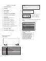
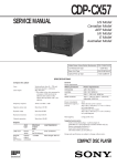
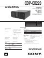
CDP-CX220
SERVICE MANUAL
US Model
Canadian Model
AEP Model
UK Model
E Model
Australian Model
Model Name Using Similar Mechanism
CDP-CX250
CD Mechanism Type
CDM-40B
Base Unit Type
KSM-213BKN/M-N
Optical Pick-up Type
KSS-213B/S-N
SPECIFICATIONS
General
Power requirements
Compact disc player
Laser
Semiconductor laser (λ = 780 nm)
Emission duration: continuous
Max 44.6 µW*
* This output is the value measured at
a distance of 200 mm from the
objective lens surface on the
Optical Pick-up block with 7 mm
aperture.
Laser output
Where purchased
Power requirements
USA/Canada
120 V AC, 60 Hz
Australia
240 V AC, 50/60 Hz
Europe
220 V – 230 V AC, 50/60 Hz
Other countries
110 V – 120 V or 220 V – 240 V AC,
adjustable, 50/60 Hz
Power consumption
Dimensions (approx.)
(w/h/d)
12 W
When the front cover is closed
430 × 200 × 480 mm (17 × 7 7/8 × 19 in.)
incl. projecting parts
More than 98 dB
Mass (approx.)
9.5 kg (21 lbs)
Harmonic distortion
Less than 0.0045%
Channel separation
More than 97 dB
Supplied accessories
Audio cord (2 phono plugs – 2 phono plugs) (1)
Remote commander (remote) (1)
Sony SUM-3 (NS) batteries (2)
CD booklet holders (2) and label (1)
Frequency response
20 Hz to 20 kHz ± 0.5 dB
Signal-to-noise ratio
More than 105 dB
Dynamic range
Outputs
Jack
type
Maximum
output
level
Load impedance
LINE OUT
Phono
Jacks
2V
(at 50 kilohms)
Over 10 kilohms
DIGITAL
OUT
(OPTICAL)
Optical
output
connector
–18 dBm
Wave length: 660 nm
MICROFILM
Design and specifications are subject to change without notice.
COMPACT DISC PLAYER
TABLE OF CONTENTS
CAUTION
1.
SERVICING NOTES ............................................... 3
2.
GENERAL ................................................................... 6
3.
DISASSEMBLY ......................................................... 7
4.
TEST MODE .............................................................. 10
5.
MECHANICAL ADJUSTMENTS ....................... 13
6.
ELECTRICAL ADJUSTMENTS ......................... 19
7. DIAGRAMS .................................................................
7-1. Note for Printed Wiring Boards and
Schematic Diagrams .......................................................
7-2. Printed Wiring Board – BD Section – ...........................
7-3. Schematic Diagram – BD Section – ...............................
7-4. Printed Wiring Board – Main Section – ........................
7-5. Schematic Diagram – Main Section – ...........................
7-6. Printed Wiring Boards – Jack Section – ........................
7-7. Schematic Diagram – Jack Section – ............................
7-8. Printed Wiring Boards – Panel Section – ......................
7-9. Schematic Diagram – Panel Section – ..........................
7-10. Printed Wiring Board – Sensor/Motor Section – ..........
7-11. Schematic Diagram – Sensor/Motor Section – .............
7-12. IC Pin Function Description ...........................................
Use of controls or adjustments or performance of procedures
other than those specified herein may result in hazardous
radiation exposure.
The laser component in this product
is capable of emitting radiation
exceeding the limit for Class 1.
This appliance is classified as
a CLASS 1 LASER product.
The CLASS 1 LASER
PRODUCT MARKING is
located on the rear exterior.
22
23
25
27
29
31
33
35
37
39
41
43
47
(Except for the customers in the United States and
Canada)
The following caution label is located inside the unit.
CAUTION
: INVISIBLE LASER RADIATION WHEN
INTERLOCKS DEFEATED. AVOID EXPOSURE TO BEAM.
OPEN
AND
ADVARSEL :
USYNLIG LASERSTRÅLING VED ÅBNING NÅR
SIKKERHEDSAFBRYDERE ER UDE AF FUNKTION. UNDGÅ UDSAETTELSE
FOR STRÅLING.
VORSICHT :
UNSICHTBARE LASERSTRAHLUNG, WENN
ABDECKUNG GEÖFFNET UND SICHEREITSVERRIEGELUNG
ÜBERBRÜCKT. NICHT DEM STRAHL AUSSETZEN.
VARO !
: AVATTAESSA JA SUOJALUKITUS OHITETTAESSA OLET ALTTIINA NÄKYMÄTTÖMÄLLE LASERSÄTEILYLLE. ÄLÄ KATSO SÄTEESEEN.
VARNING
: OSYNLING LASERSTRÅLING NÄR DENNA DEL ÄR ÖPPNAD
OCH SPÄRREN ÄR URKOPPLAD. BETRAKTA EJ STRÅLEN.
ADVERSEL :
8.
EXPLODED VIEWS ................................................ 49
9.
ELECTRICAL PARTS LIST ............................... 56
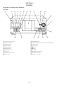
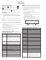
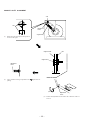
MODEL IDENTIFICATION
— BACK PANEL —
PART No.
PART No.
MODEL
4-998-525-0
US model
4-998-525-1
Canadian model
4-998-525-2
AEP, AED UK model
4-998-525-4
Singapore model
4-998-525-5
E model
4-998-525-6
Australian model
• Abbreviation
AED: North European
–2–
USYNLIG LASERSTRÅLING NÅR DEKSEL ÅPNES OG
SIKKERHEDSLÅS BRYTES. UNNGÅ EKSPONERING FOR STRÅLEN.
VIGYAZAT ! :
A BURKOLAT NYITÁSAKOR LÁTHATATLAN LÉZERSUGÁRVESZÉLY! KERÜLJE A BESUGÁRZÁST!
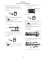
SECTION 1
SERVICING NOTES
SAFETY CHECK-OUT
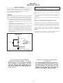
After correcting the original service problem, perform the following safety check before releasing the set to the customer:
Check the antenna terminals, metal trim, “metallized” knobs,
screws, and all other exposed metal parts for AC leakage.
Check leakage as described below.
LEAKAGE
The AC leakage from any exposed metal part to earth ground and
from all exposed metal parts to any exposed metal part having a
return to chassis, must not exceed 0.5 mA (500 microampers.).
Leakage current can be measured by any one of three methods.
1. A commercial leakage tester, such as the Simpson 229 or RCA
WT-540A. Follow the manufacturers’ instructions to use these
instruments.
2. A battery-operated AC milliammeter. The Data Precision 245
digital multimeter is suitable for this job.
3. Measuring the voltage drop across a resistor by means of a
VOM or battery-operated AC voltmeter. The “limit” indication is 0.75 V, so analog meters must have an accurate lowvoltage scale. The Simpson 250 and Sanwa SH-63Trd are examples of a passive VOM that is suitable. Nearly all battery
operated digital multimeters that have a 2 V AC range are suitable. (See Fig. A)
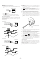
NOTES ON HANDLING THE OPTICAL PICK-UP
BLOCK OR BASE UNIT
The laser diode in the optical pick-up block may suffer electrostatic break-down because of the potential difference generated
by the charged electrostatic load, etc. on clothing and the human
body.
During repair, pay attention to electrostatic break-down and also
use the procedure in the printed matter which is included in the
repair parts.
The flexible board is easily damaged and should be handled with
care.
NOTES ON LASER DIODE EMISSION CHECK
The laser beam on this model is concentrated so as to be focused
on the disc reflective surface by the objective lens in the optical
pick-up block. Therefore, when checking the laser diode emission, observe from more than 30 cm away from the objective lens.
LASER DIODE AND FOCUS SEARCH OPERATION
CHECK
Carry out the “S curve check” in ”CD section adjustment” and
check that the S curve waveform is output repeatedly.
To Exposed Metal
Parts on Set
0.15 µF
1.5 k Ω
AC
voltmeter
(0.75 V)
Earth Ground
Fig. A. Using an AC voltmeter to check AC leakage.
SAFETY-RELATED COMPONENT WARNING!!
ATTENTION AU COMPOSANT AYANT RAPPORT
À LA SÉCURITÉ!
COMPONENTS IDENTIFIED BY MARK ! OR DOTTED
LINE WITH MARK ! ON THE SCHEMATIC DIAGRAMS
AND IN THE PARTS LIST ARE CRITICAL TO SAFE
OPERATION. REPLACE THESE COMPONENTS WITH
SONY PARTS WHOSE PART NUMBERS APPEAR AS
SHOWN IN THIS MANUAL OR IN SUPPLEMENTS PUBLISHED BY SONY.
LES COMPOSANTS IDENTIFIÉS PAR UNE MARQUE !
SUR LES DIAGRAMMES SCHÉMATIQUES ET LA LISTE
DES PIÈCES SONT CRITIQUES POUR LA SÉCURITÉ
DE FONCTIONNEMENT. NE REMPLACER CES COMPOSANTS QUE PAR DES PIÈCES SONY DONT LES
NUMÉROS SONT DONNÉS DANS CE MANUEL OU
DANS LES SUPPLÉMENTS PUBLIÉS PAR SONY.
–3–
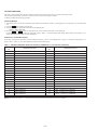
CD-TEXT TEST DISC
This unit is able to display the test data (character information) written in the CD on its fluorescent indicator tube.
The CD-TEXT TEST DISC (TGCS-313:4-989-366-01) is used for checking the display.
To check, perform the following procedure.
Checking Method:
1. Turn ON the power, set the disc on the disc table with the side labeled as “test disc” as the right side, close the front cover, and chuck the
disc.
2. Press the · button and play back the disc.
3. The following will be displayed on the fluorescent indicator tube.
Display : 1kHz/0 dB/ L&R
4. Press the ≠ and ± buttons to switch the track. The text data of each track will be displayed.
For details of the displayed contents for each track, refer to “Table 1 : CD-TEXT TEST DISC TEXT Data Contents” and “Table 2 : CDTEXT TEST DISC Recorded Contents and Display”.
Restrictions in CD-TEXT Display
In this unit, some special characters will not be displayed properly. These will be displayed as a space or a character resembling it. For
details, refer to “Table 2 : CD-TEXT DISC Recorded Contents and Display”.
Table 1 : CD-TEXT TEST DISC TEXT Data Contents (TRACKS No. 1 to 41:Normal Characters)
TRACK
No.
Displayed Contents
TRACK
Displayed Contents
No.
1
1kHz/0dB/L&R
22
1kHz/-90dB/L&R
2
20Hz/0dB/L&R
23
Infinity Zero w/o emphasis//L&R
3
40Hz/0dB/L&R
24
Infinity Zero with emphasis//L&R
4
100Hz/0dB/L&R
25
400Hz+7kHz(4:1)/0dB/L&R
5
200Hz/0dB/L&R
26
400Hz+7kHz(4:1)/-10dB/L&R
6
500Hz/0dB/L&R
27
19kHz+20kHz(1:1)/0dB/L&R
7
1kHz/0dB/L&R
28
19kHz+20kHz(1:1)/-10dB/L&R
8
5kHz/0dB/L&R
29
100Hz/0dB/L*
9
7kHz/0dB/L&R
30
1kHz/0dB/L*
10
10kHz/0dB/L&R
31
10kHz/0dB/L*
11
16kHz/0dB/L&R
32
20kHz/0dB/L*
12
18kHz/0dB/L&R
33
100Hz/0dB/R*
13
20kHz/0dB/L&R
34
1kHz/0dB/R*
14
1kHz/0dB/L&R
35
10kHz/0dB/R*
15
1kHz/-1dB/L&R
36
20kHz/0dB/R*
16
1kHz/-3dB/L&R
37
100Hz Squer Wave//L&R
17
1kHz/-6dB/L&R
38
1kHz Squer Wave//L&R
18
1kHz/-10dB/L&R
39
1kHz w/emphasis/-0.37dB/L&R
19
1kHz/-20dB/L&R
40
5kHz w/emphasis/-4.53dB/L&R
20
1kHz/-60dB/L&R
41
16kHz w/emphasis/-9.04dB/L&R
21
1kHz/-80dB/L&R
NOTE: The contents of Track No. 1 to 41 are the same as those of the current TEST DISC-their titles are displayed.
–4–
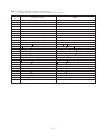
Table 2: CD-TEXT TEST DISC Recorded Contents and Display
(In this unit, some special characters cannot be displayed. This is no a fault.)
TRACK
Recorded Contents
No.
42
! ” # $%& ´
Display
(21h to 27h)1kHz 0dB L&R
N All the same
43
( )* + , – . /
(28h to 2Fh)
N All the same
44
01234567
(30h to 37Fh)
N All the same
45
89 : ; <=>?
(38h to 3Fh)
N All the same
46
@A B C D E F G
(40h to 47Fh)
N All the same
47
H I J K L MNO
(48h to 4Fh)
N All the same
48
P Q R S T U VW
(50h to 57Fh)
PQ R S T U V W (50h to 57h)
49
XYZ [ ¥ ] ^ _
(58h to 5Fh)
XY Z [ \ ] ^ _ (58····
50
′
(60h to 67Fh)
′
51
h i j k l mn o
(68h to 6Fh)
N All the same
52
pq r s t u vw
(70h to 77Fh)
p q r s t u v w (70h to 77h)
53
x y z { I } ~
(78h to 7Fh)
xy z {
i ¢£¤¥ §
¬ PR –
54
55
56
ab c de f g
≥C ª
•
57
†
58
±
1
2
º
3
′
1
4
µ¶ •
1
2
3
4
} ~
i ¢£¤¥
(78····
§ (A0····
is not displayed
(A8···· C ª ¬ P R – are not displayed
≥
(A8h to AFh)
′
(B0h to B7h)
µ
• (B0···· • ±
1
¶ are not displayed
1
4
†
À Á Â Ã Ä Å ÆÇ
(C0h to C7Fh)
ÀÁ Â Ã Ä Å ÆÇ (C0h to C7h)
59
ÈÉÊË Ì Í Î Ï
(C8h to CFh)
N All the same
60
D ÑÒÓÔÕÖ
(D0h to D7Fh)
D ÑÒÓ Ô Õ Ö
61
62
˙ ß
ØÙÚÛÜY
à á â ã ä åæç
(D8h to DFh)
(E0h to E7h)
´ ß (D8····
ÙÚÛÜY
à á â ã ä å æ ç (E0h to E7h)
63
èéêë ì í î ï
(E8h to EFh)
N All the same
64
∂ ñòóôõö÷
(F0h to F7Fh)
65
ø ù ú û ü y´
(F8h to FFFh)
66
No.66
N All the same
67
No.67
N All the same
to
to
No.99
ÿ
¿ (B8···· º
2 3
(B8h to BFh)
99
¿
(A0h to A7h) 8859-1
a b c d e f g (60h to 67h)
(D0h to D7h)
ñ ò ó ô õ ö ÷ (F0h to F7h)
ø ù ú û ü y´
ÿ (F8h to FFh)
to
N All the same
–5–
1
2
3
4
are not displayed
SECTION 2
GENERAL
LOCATION OF PARTS AND CONTROLS
Front Panel
1
2
3
4
5
6
7
8
9
!¡
!º
!™
STANDBY
1/u
!£
DISC/CHARACTER
INPUT
MEMO SEARCH
PUSH ENTER
CONTINUE SHUFFLE PROGRAM
REPEAT
TIME/TEXT
AMS
±
GROUP 1
GROUP 2
GROUP 3
GROUP 4
GROUP 5
GROUP 6
GROUP 7
GROUP 8
±
CHECK
CLEAR
P
p
OPEN/CLOSE
ª
§
GROUP FILE
!¢
@º
!ª
!•
!¶
!§
!∞
1 I/u (power switch) button
!¡ ≠/± buttons
2 CONTINUE button
!™ JOG dial (DISC/CHARACTER/PUSH ENTER knob)
3 SHUFFLE button
!£ CHECK button
4 Display window
!¢ CLEAR button
5 PROGRAM button
!∞ p button
6 REPEAT button
!§ P button
7 TIME/TEXT button
!¶ · button
8 Front cover
!• § (OPEN/CLOSE) button
9 MEMO SEARCH button
!ª GROUP FILE button
!º INPUT button
@º GROUP 1 – 8 buttons
–6–
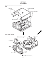
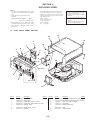
SECTION 3
DISASSEMBLY
Note: Follow the disassembly procedure in the numerical order given.
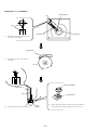
CASE
1 four screws
(case 3 TP2)
3 Remove the case to
direction of arrow A.
1 five screws
(case 3 TP2)
A
2 Open the case.
FRONT PANEL SECTION
6 Remove the door (CD) ass’y
to direction of arrow A.
2 four screws
(BVTP3 × 8)
A
4 claw
4 claw
5 front panel section
3 five screws (BVTT3 × 6)
–7–
1 flat wire (CN501)
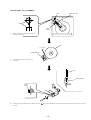
GUIDE ASS’Y
3 three screws
(BVTT3 × 6)
4 boss
5 guide ass’y
3 three screws
(BVTT3 × 6)
2 screw
(PSW3 × 6)
1 connector
(CN503)
REAR PANEL SECTION
3 three connectors
(CN504, 506, 507)
1 connector
(CN505)
2 flat wire
(CN502)
6 rear panel section
4 five screws
(BVTT3 × 6)
1 connector
(CN904)
3 four screws
(PTTWH3 × 6)
5 PC board
holder
7 four screws
(BVTT3 × 6)
–8–
8 bracket
MECHANISM DECK
2 mechanism deck
1 three screws
(BVTT3 × 8)
1 six screws
(BVTT3 × 8)
BASE UNIT
1 screw (BVTT3 × 8)
2 fulcrum plate
(BU upper) ass’y
3 base unit
–9–
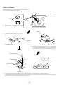
SECTION 4
TEST MODE
DISPLAY CHECK MODE
With the power turned off (standby state), press the I/u button
while pressing the P (pause) button.
All FL segments and grids light up together with the · (play),
P (pause), and standby LEDs.
At the same time, the GROUP LEDs are scanned one by one.
KEY AND FLUORESCENT DISPLAY TUBE CHECK
MODE
1. Connect the test point (TP:AFADJ) of the MAIN board to the
Ground, and insert the power plug to the outlet to set this mode.
First, the external SRAM is checked, and if abnormal, “SRAM
NG” is displayed.
If OK, the following steps are performed.
Note: To exit this mode, press the p (stop) button.
* Fluorescent Display Tube Check Mode
The whole fluorescent display tube lights up when the connection in step 1 is made.
* Key Check Mode
This mode is set when a button is pressed after the whole
fluorescent display tube lights.
All buttons have a button number.
When a button is pressed, the counter display is counted up,
and the number of that button is displayed.
However, the counter display will only count up to 26, but
the number of buttons pressed will always be displayed.
ADJ MODE
1. Turn ON the power of the unit, set disc to disc table, and perform chucking.
2. Disconnect the power supply plug from the outlet.
3. To set ADJ mode, connect the test point (TP: ADJ) of the MAIN
board to Ground, and connect the power supply plug to the
outlet.
The power will turn on automatically, and the first track will be
played.
In this mode, table rotation and loading operations are not performed because it is taken that the disc has already been chucked.
O
Note: The same operations are also performed in the following when the
test point (TP: ADJ) is connected to Ground after turning on the
power.
• Direct search (movement of sledding motor) is not performed
during accessing
• Ignored even when GFS becomes L
• Ignored even when the Q data cannot be read
• Focus gain does not decrease
• Spindle gain does not decrease
• Servo related settings can be set manually and checked (Refer
to ADJ Mode Special Functions Table)
**
Counter display
CONTINUE
SHUFFLE
PROGRAM
Button Number or Display
Servo average display
Displays VC, FE, RF, TE and traverse in hexadecimal
numbers
Button number display
Buttons and Corresponding Button Numbers
Button
CLEAR
ADJ Mode Special Functions Table
(The buttons shown with ( ) function by using the supplied remote commander only)
Button
**
Button Number or Display
3
CHECK
4
± (AMS)
5
≠ (AMS)
6
PUSH ENTER
7
§ (OPEN/CLOSE)
9
INPUT
10
MEMO SEARCH
11
Focus bias display
Each time this is pressed, the focus bias is switched
between 1 and 2
1
Bias actually set Optimum bias Minimum jitter
2
U:Upper aliasing bias L:Lower aliasing bias
I/u
18
TIME/TEXT
19
GROUP FILE
20
GROUP 8
21
GROUP 7
22
GROUP 6
23
GROUP 5
24
REPEAT
27
Auto gain display
Displays focus, tracking, sledding in hexadecimal
numbers
PROGRAM
28
GROUP 1 (1)
Increases the focus bias in 8 steps.
SHUFFLE
29
GROUP 2 (2)
Sets the focus bias in the middle of aliasing.
CONTINUE
30
GROUP 3 (3)
Turns off the tracking and sledding servo
GROUP 4
31
GROUP 4 (4)
Returns the auto gain to the initial value (30)
GROUP 3
32
GROUP 5 (5)
Turns off the focus servo
GROUP 2
33
GROUP 6 (6)
Decreases the focus bias in 8 steps.
GROUP 1
34
GROUP 7 (7)
Re-adjusts the focus bias
·
All lit (LED lit)
GROUP 8 (8)
Turns on the tracking and sledding servo
P
Partial lighting 1 (LED lit)
Switches the focus servo gain between normal and down
FG. norm: normal, FG. down: down
p
Partial lighting 2
(9)
(10/0)
Sets the focus bias to 0 (no bias)
Next, displays the jitter measured at the focus bias set
CHECK
S-curve observation mode
CLEAR
Automatic eccentric measurement
The results of measurement is displayed in mm directly.
– 10 –
DISC/
CHARACTER
Partial lighting 3
• When the jog dial is rotated to the right, the
GROUP LEDs light up in the order of 1 → 2..8
→ 2nd → 1.
• When the jog dial is rotated to the left, the
GROUP LEDs light up in the order of 8 → 7..1
→ 2nd → 8.
Partial lighting 1
AGING MODE
O
A B C D E F G
Partial lighting 2
O
• Mode which repeatedly changes and plays back discs automatically in the unit.
• It will repeat aging as long as no errors occur.
• If an error occurs during aging, it will stop all servos, motors,
etc. instantaneously, display the error number, and stop operations. However, the stopping conditions differ according to
whether the unit is equipped with the “self-protection function
during errors” described later.
The function serves to maintain the state of the unit when errors
occur.
Sequence of Aging Mode
Order of Disc Change
(1 cycle takes 3 minutes)
$
1. Disc change
$
1. No. 40
Partial lighting 3
$
2. Load in
O
$
2. No. 120
2nd
$
3. TOC read
**
*: Counter displayed
$
3. No. 80
$
4. Access of last track
$
4. No. 200
Test Points Location:
$
5. 3 second playback
[MAIN BOARD] – Component Side –
$
6. Access of first track
IC502
TP
(AFADJ)
TP
(ADJ)
IC501
$
5. No. 160
$
$
7. 3 second playback
IC506
$
8. Load out
$
CN509
CN508
Special Functions in Aging Mode
1. Disc setting mode:
5 discs are set before setting the aging mode. This mode makes
the setting of these discs more easy.
2. Self protection function during errors:
Function which voluntarily corrects errors which occur during normal operations by retries.
If this function is not provided, all operations will be stopped
without retiring. It is suitable for checking errors with low reproducibility.
If this function is provided, and errors can be corrected by
retries, aging will be continued without stopping.
3. Aging cycle count function:
Functions which displays the number of agings carried out on
the Fluorescent indicator tube in numbers. One aging cycle
consists of five discs.
number of agings
1DISC
CD1
DISC
*DISC-40*
– 11 –
2
Aging Method
1. Change the [COMMAND MODE] switch (S901) on set to
[CD1].
2. Turn ON the power of the unit. Open the front cover.
3. Press the [AGING START] button of the remote commander
for aging mode (J-2501-123-A).
4. When the disc set mode is set, the · and P LEDs blink.
5. Rotate the JOG dial. The slits (No. 40, 80, 120, 160, 200) for
setting the discs will come forward. Insert the discs into these
slits. Do not set the discs in other slits.
6. Set whether the self-protection function during errors is
equipped with the unit. Press the [REPEAT] button. If “REPEAT” is displayed on the Fluorescent indicator tube, it means
the function is provided. If “REPEAT” is not displayed, it
means the function is not provided.
7. Press the · button.
8. The · LED blinks, the aging mode is set, and aging is
started.
9. The aging cycle lasts 3 minutes. If errors occur during aging,
the error number will be displayed on the Fluorescent indicator tube. (Refer to the following table for the details of the
errors.)
10. Aging will be repeated as long as no errors occur.
11. After each aging cycle, the number displayed on the Fluorescent indicator tube will increase.
12. To end aging, press the I/u button
Error Display
Err01
120
Disc number
Error code
Error code
Code number
Name
Contents
Err 01
DISC sensor check 1
No disc in the specified slit
Err 02
DISC sensor check 2
Disc in other slits
Err 03
Table operation check 1
Table motor current over
Err 04
Table operation check 2
No table sensor input
Err 05
Loading operation check 1
Load in timeover
Err 06
Loading operation check 2
Load out timeover
Err *1
BU related check 1
Access timeover
Err *2
BU related check 2
High speed search NG
Err *3
BU related check 3
Q data read error
Err *4
BU related check 4
BU operation (from focus search to until signal can be read) timeover
Err *5
BU related check 5
GFS monitor error
Err *6
BU related check 6
Focus cannot be imposed by focus search
Err *7
BU related check 7
Auto focus bias adjustment cannot be performed
The * numbers mean the following according to the state of the unit during aging
2 : From checking to end of TOC read
3 : From end of TOC read to end of last track playback
4 : From end of last track playback to end of first track playback
– 12 –
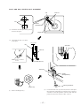
SECTION 5
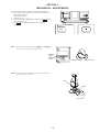
MECHANICAL ADJUSTMENTS
Perform the following steps before carrying out adjustments.
1. Turn ON the power of the unit, set disc to disc table No. 92,
and perform chucking.
2. Turn OFF the power.
3. Remove the case.
4. While pressing the [STOP] button, turn ON the I/u button.
The test mode is set.
5. The I/u button LED (STANDBY) starts blinking.
(Test mode)
LED (STANDBY)
1/u
p
1/u button
STOP button
Note 1: The cam will start rotating when the [GROUP 1] or [GROUP 5]
button is pressed continuously in the test mode.
GROUP 1
button
GROUP 5
button
GROUP 1 button
GROUP 5 button
Note 2: If the power cannot be supplied, the cam can be rotated by rotating the pulley with your finger.
cam
pulley
– 13 –
GUIDE (DISC T) ALIGNMENT
holder (guide T)
cam
cam
fixed screw
guide (disc T)
(1)
Rotate the cam and adjust to the position shown in the figure.
guide (disc T)
(2)
Check that the state is as shown in
the figure.
disc
A
B
tapering screwdriver
guide (disc T)
disc
holder (guide T)
(3)
Loosen the fixed screw by about 60 °.
(4)
holder
(guide T)
– 14 –
Move the holder (guide T) with a tapering screwdriver,
and set the position of the guide (disc T) to A:B=1:1.
HOLDER (DISC A2) ALIGNMENT
cam
holder (disc A2)
cam
thrust
screw
(1)
Rotate the cam and adjust to the position
shown in the figure.
disc
0 – 1 mm
holder (disc A2)
(2)
Check that the state is as shown in
the figure.
disc
holder (disc A2)
thrust
screw
(3)
123
After applying suitable locking compound to the 123 part, rotate the thrust screw until the holder (Disc A2) comes to the center of
the disc.
– 15 –
SENSOR ALIGNMENT
Perform this adjustment after the “holder (disc A2) adjustment”.
If the disc table swings to the left and right just before the disc is
chucked, perform the following adjustment.
cam
lever (stopper) ass’y
cam
(1)
Rotate the cam and adjust to the position
shown in the figure.
bracket (sensor)
table ass’y
(2)
Check that the lever (stopper) ass’y secures
the disc table as shown in the figure.
disc table
swing
lever (stopper) ass’y
(4)
Moving the disc table right and left with a hand after the
screw is fixed, the table will move by the play of a disc table.
If the LEDs light up alternately, the adjustment will be performed correctly.
tapering screwdriver
LUMINOUS board
PLAY button
PAUSE button
bracket (sensor)
fixed screw
(3)
Loosen the fixed screw by 60° to 90°, and use a tapering screwdriver to adjust the screw as shown in the figure.
Move the bracket (sensor) with the tapering screwdriver little by little, and fix the fixed screw at where the play button's LED (green)
is switched to the pause button's LED (orange) (or its reverse).
– 16 –
PULLY AND DISC CENTER HOLE ALIGNMENT
cam
base unit
cam
bracket
(BU adjustment)
(1)
(2)
Rotate the cam and adjust to the position
shown in the figure.
magnet ass’y
Check that the state is as shown
in the figure.
0.5 – 2 mm
disc
disc pulley
disc hole
base unit
Note: The disc should not
be fixed.
holder (disc A2)
fixed screw
bracket
(BU adjustment)
tapering screwdriver
magnet ass’y
(3)
Remove the Magnet ass’y.
(4)
– 17 –
Loosen the fixed screw by 60° to 90°, and move and adjust
the bracket (BU adjustment) up and down using a tapering
screwdriver so that the positions of the disc hole and disc
pulley become A=B or between A:B=2:1 and 1:2.
MAGNET ASS’Y ALIGNMENT
cam
cam
adjustment
screw
magnet ass’y
(1)
Rotate the cam and adjust to the position
shown in the figure.
disc
magnet holder
magnet ass’y
adjustment
screw
A
(3)
B
1234
1234
Apply suitable locking compaund to the1234 part after adjusting.
adjustment
screw
(2)
– 18 –
Rotate the adjustment screw until A=B or between A:B=2:1
and 1:2
SECTION 6
ELECTRICAL ADJUSTMENTS
Note:
1. CD Block is basically designed to operate without adjustment. Therefore, check each item in order given.
2. Use YEDS-18 disc (3-702-101-01) unless otherwise indicated.
3. Use an oscilloscope with more than 10MΩ impedance.
4. Clean the object lens by an applicator with neutral detergent when the
signal level is low than specified value with the following checks.
Note: A clear RF signal waveform means that the shape “◊” can be clearly
distinguished at the center of the waveform.
RF signal waveform
VOLT/DIV: 200 mV
TIME/DIV: 500 ns
S-Curve Check
level: 1.2
oscilloscope
+0.25
–0.20 Vp-p
BD board
TP (FE1)
TP (VC)
+
–
E-F Balance Check
Procedure :
1. Connect oscilloscope to test point TP (FE1) on BD board.
2. Connect test point TP (ADJ) on MAIN board to ground with
lead wire.
3. Turn I/u button on to set the ADJ mode.
4. Put disc (YEDS-18) in and playback.
Press the [CHECK] button.
5. Check the oscilloscope waveform (S-curve) is symmetrical between A and B. And confirm peak to peak level within 3 ± 1
Vp-p.
S-curve waveform
symmetry
A
within 3 ± 1 Vp-p
oscilloscope
BD board
TP (TE)
TP (VC)
+
–
Procedure :
1. Connect oscilloscpe to test point TP (TE) on BD board.
2. Connect the test point TP (ADJ) on MAIN board to the ground
with a lead wire.
3. Turn the I/u button on to set the ADJ mode.
4. Put disc (YEDS-18) in to play the number five track.
5. Press the [GROUP 3] button. (The tracking servo and the sledding servo are turned OFF.)
6. Check the level B of the oscilliscope's waveform and the A
(DC voltage) of the center of the Traverse waveform.
Confirm the following :
A/B x 100 = less than ± 22%
B
Traverse waveform
Center of the waveform
6. After check, remove the lead wire connected in step 2.
Note: • Try to measure several times to make sure than the ratio of A : B
or B : A is more than 10 : 7.
• Take sweep time as long as possible and light up the brightness
to obtain best waveform.
B
A (DC voltage)
0V
RF Level Check
level: 1.3 ± 0.6 Vp-p
oscilloscope
(AC range)
7. Press the [GROUP 8] button. (The tracking servo and sledding servo are turned ON.) Confirm the C (DC voltage) is
almost equal to the A (DC voltage) is step 6.
BD board
TP (RFO)
TP (VC)
+
–
Traverse waveform
Procedure :
1. Connect oscilloscope to test point TP (RFO) on BD board.
2. Turn I/u button on.
3. Put disc (YEDS-18) in to play the number five track.
4. Confirm that oscilloscope waveform is clear and check RF signal level is correct or not.
C (DC
voltage)
0V
Tracking servo
Sled servo
OFF
Tracking servo
Sled servo
ON
8. Disconnect the lead wire of TP (ADJ) connected in step 1.
– 19 –
RF PLL Free-run Frequency Check
Procedure :
1. Connect frequency counter to test point TP (XPCK) with lead
wire.
frequency counter
BD board
TP (XPCK)
+
–
2. Turn I/u button on.
3. Put the disc (YEDS-18) in to play the number five track.
Confirm that reading on frequency counter is 4.3218MHz.
Procedure:
1. Connect the oscilloscope to Pins 1, 2, and 4 of CN506 of
the MAIN board. Also connect a 1 kΩ resistor to Pin 4 at the
same time. (Connection 1)
2. Check that no discs are loaded in the unit, and press the
I/u button while pressing the [INPUT] button.
3. The rotary table will continue rotating in the clockwise direction.
4. Observe the waveform at that time on the oscilloscope.
5. Loosen the screw securing the LUMINOUS board slightly.
6. Slide the LUMINOUS board to the left and right so that the
peak of the D0 waveform is at the center between the descending point of the T1 waveform and ascending point of the T2
waveform. (Waveform 1) After adjusting, apply locking compound.
Disc Sensor Adjustment
Perform this adjustment after completing all adjustments of the
mechanism section.
If not performed accurately, the presence of the disc may not be
detected properly.
Connection 1:
CN506 of MAIN board
T1: Pin 1 (T. SENS 1)
T2: Pin 2 (T. SENS 2)
D0: Pin 4 (D. SENS)
oscilloscope
1 kΩ
+
–
LUMINOUS board
Waveform 1:
A B
T1
T2
D0
7. Disconnect the resistor connected to Pin 4 of CN506 of the
MAIN board. (Connection 2)
8. Observe the waveform on the oscilloscope. (Waveform 2)
9. Adjust RV501 of the MAIN board so that the waveform on the
oscilloscope satisfies the following adjustment value.
10. After the adjustment, load a disc only in slit 1, close the front
cover, and press the I/u button to turn off the power.
11. Press the I/u button while pressing the [PUSH ENTER] button
to turn on the power.
12. If the rotary table makes round, and “YES” is displayed on the
fluorescent indicator tube after it stops, it means that the adjustment has been performed properly.
Connection 2:
CN506 of MAIN board
T1: Pin 1 (T. SENS 1)
T2: Pin 2 (T. SENS 2)
D0: Pin 4 (D. SENS)
oscilloscope
+
–
Adjustment value:
At the shoulder part of waveform D1, T1 becomes H and T2 becomes L, and at the same time, the Y width must not be smaller
than 1/4 of the Z width.
In order to satisfy this value more easily, adjust so that X=Y approximately and observe the deviation of the waveform.
Waveform 2
Z
X Y
T1
T2
D1
– 20 –
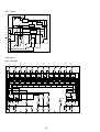
Adjustment Location:
[BD BOARD] – Side B –
TP
(XPCK)
IC101
TP
(FE)
TP (RFO)
TP
(VC)
TP (TE)
TP
(FE1)
TP
(FE2)
IC103
[MAIN BOARD] – Component Side –
CN501
CN506
6
1
RV501
IC502
TP
(ADJ)
TP
(AFADJ)
IC501
CN509
CN508
– 21 –
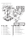
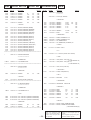
SECTION 7
DIAGRAMS
• Circuit Boards Location
ILLUMINATION board
D. SENS (RAY CATCHER) board
MAIN board
D. SENS (LUMINOUS) board
DISP board
JACK board
T. SENS board
T. MOTOR board
DOOR SN board
DOOR MOTOR board
JOG board
BD board
L. SW board
L. MOTOR board
– 22 –
7-1.
NOTE FOR PRINTED WIRING BOARDS AND SCHEMATIC DIAGRAMS
THIS NOTE IS COMMON FOR PRINTED WIRING BOARDS AND SCHEMATIC DIAGRAMS.
(In addition to this, the necessary note is printed in each block.)
Note on Schematic Diagram:
• All capacitors are in µF unless otherwise noted. pF: µµF
50 WV or less are not indicated except for electrolytics
and tantalums.
• All resistors are in Ω and 1/4 W or less unless otherwise
specified.
¢
•
: internal component.
• C : panel designation.
Note on Printed Wiring Boards:
• X : parts extracted from the component side.
• Y : parts extracted from the conductor side.
¢
•
: internal component.
12345678
• b
: Pattern from the side which enables seeing.
12345678
• 12345678
12345678: Solder bridge.
• Indication of transistor.
C
Note:
The components identified by mark ! or dotted
line with mark ! are critical for safety.
Replace only with part
number specified.
•
•
•
•
•
•
•
•
•
Note:
Les composants identifiés par
une marque ! sont critiques
pour la sécurité.
Ne les remplacer que par une
piéce por tant le numéro
spécifié.
U : B+ Line.
V : B– Line.
H : adjustment for repair.
Voltages and waveforms are dc with respect to ground
under no-signal conditions.
no mark: PLAY
Voltages are taken with a VOM (Input impedance 10 MΩ).
Voltage variations may be noted due to normal production tolerances.
Waveforms are taken with a oscilloscope.
Voltage variations may be noted due to normal production tolerances.
Circled numbers refer to waveforms.
Signal path.
J : CD
c : digital out
Abbreviation
AED : North European
AUS : Australian model.
CND : Canadian model.
E2
: 120 V AC Area in E model.
E3
: 240 V AC Area in E model.
SP
: Singapore model.
Q
These are omitted.
B E
Q
B
C
E
These are omitted.
Q
B
C
E
These are omitted.
– 23 –
• Waveforms
– BD Section –
– PANEL Section –
1 IC101 ^§ (XTAI)
1 IC701 %• (OSC0)
3.6 Vp-p
2.5 Vp-p
16.9344 MHz
480 ns
2 IC101 %¡ (RFAC)
500 mV/DIV, 1 µs/DIV
1.2 +0.25
–0.20 Vp-p
3 IC101 $¡ (TE)
200 mV/DIV, 1 µs/DIV
Approx.
500 mVp-p
4 IC101 #ª (FE)
200 mV/DIV, 10 µs/DIV
Approx.
600 mVp-p
– MAIN Section –
1 IC501 #¡ (EXTAL)
3.6 Vp-p
10 MHz
– 24 –
7-2. PRINTED WIRING BOARD – BD Section –
• See page 22 for Circuit Boards Location.
– 25 –
(Page 30)
– 26 –
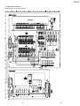
CDP-CX220
7-3. SCHEMATIC DIAGRAM – BD Section –
• See page 24 for Waveforms. • See page 44 for IC Block Diagrams.
(Page 32)
• no mark: PLAY
• Signal path.
J : CD
c : digital out
Note:
The components identified by mark ! or dotted
line with mark ! are critical for safety.
Replace only with part
number specified.
Note:
Les composants identifiés par
une marque ! sont critiques
pour la sécurité.
Ne les remplacer que par une
piéce por tant le numéro
spécifié.
– 27 –
– 28 –
CDP-CX220
7-4. PRINTED WIRING BOARD – MAIN Section –
• See page 22 for Circuit Boards Location.
(Page 37)
(Page 42)
(Page 41)
• Semiconductor
Location
Ref. No.
Location
D327
D501
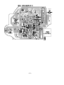
D502
D503
D504
D505
D506
D507
D508
D509
D521
E-5
E-4
E-4
E-4
E-4
E-3
E-1
E-1
E-5
E-5
B-3
IC401
IC501
IC502
IC503
IC504
IC505
IC506
C-8
C-3
B-4
C-1
D-5
D-3
C-5
Q322
Q323
Q325
Q327
Q422
Q423
Q425
Q501
Q503
Q521
E-7
E-7
E-6
E-5
E-8
E-8
E-6
E-2
C-5
A-3
(Page 41)
(Page 26)
(Page 41)
(Page 41)
(Page 33)
– 29 –
(Page 34)
– 30 –
CDP-CX220
7-5. SCHEMATIC DIAGRAM – MAIN Section –
• See page 24 for Waveforms. • See page 45 for IC Block Diagrams.
(Page 27)
(Page 43)
(Page 43)
(Page 36)
(Page 43)
(Page 43)
(Page 43)
(Page 40)
(Page 35)
• no mark: PLAY
• Signal path.
J : CD
c : digital out
– 31 –
– 32 –
CDP-CX220
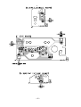
7-6. PRINTED WIRING BOARDS – JACK Section –
• See page 22 for Circuit Boards Location.
(Page 29)
(Page 30)
– 33 –
– 34 –
CDP-CX220
7-7. SCHEMATIC DIAGRAM – JACK Section –
(Page 32)
• no mark: PLAY
• Signal path.
J : CD
c : digital out
Note:
The components identified by mark ! or dotted
line with mark ! are critical for safety.
Replace only with part
number specified.
(Page 32)
Note:
Les composants identifiés par
une marque ! sont critiques
pour la sécurité.
Ne les remplacer que par une
piéce por tant le numéro
spécifié.
– 35 –
– 36 –
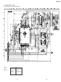
7-8. PRINTED WIRING BOARDS – PANEL Section –
• See page 22 for Circuit Boards Location.
(Page 38)
(Page 29)
– 37 –
(Page 38)
(Page 37)
(Page 37)
• Semiconductor
Location
(DISP Board)
Ref. No.
Location
D701
D702
D703
D704
D705
D706
D707
D708
D709
F-4
F-3
F-3
F-2
F-4
F-3
F-3
F-2
A-5
IC601
IC701
IC702
B-2
C-2
D-1
Q701
D-3
– 38 –
CDP-CX220
7-9. SCHEMATIC DIAGRAM – PANEL Section –
• See page 24 for Waveforms. • See page 46 for IC Block Diagrams.
(Page 31)
– 39 –
– 40 –
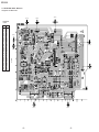
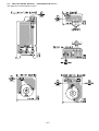
7-10. PRINTED WIRING BOARDS – SENSOR/MOTOR Section –
• See page 22 for Circuit Boards Location.
(Page 30)
(Page 30)
(Page 29)
(Page 29)
– 41 –
(Page 29)
– 42 –
CDP-CX220
7-11.
SCHEMATIC DIAGRAM – SENSOR/MOTOR Section –
(Page 31)
(Page 31)
(Page 31)
(Page 31)
(Page 31)
– 43 –
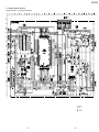
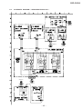
• IC Block Diagrams
– BD Board –
PCO
FILI
FILO
CLTV
AVSS3
RFAC
BIAS
ASYI
ASYO
AVDD0
IGEN
AVSS0
ADIO
RFDC
CE
TE
60
59 58 57
56 55 54 53
52
51 50 49 48
47
46 45
44
43 42 41
DIGITAL
OUT
LRCK 61
PCMD 62
D/A
INTERFACE
INTERNAL BUS
VDD
VSS
AVDD3
CXD2587Q
DOUT
IC101
ERROR
CORRECTOR
DIGITAL
PLL
16K
RAM
40 SE
39 FE
38 VC
ASYMMETRY
CORRECTION
OPERATIONAL
AMPLIFIER
ANALOG SWITCH
EFM
DEMODULATOR
A/D
CONVERTER
BCK 63
EMPH 64
XVDD 65
66
67
68
69
70
71
TIMING
LOGIC
CLOCK
GENERATOR
SERVO DSP
LOUT1 72
PWM
AVSS1 73
AVSS2 74
LOUT2 75
PWM
3rd ORDER
NOISE SHAPER
OVER SAMPLING
DIGITAL FILTER
AIN2 76
AOUT2 77
AVDD2 78
RMUT 79
LMUT 80
SUBCODE
PROCESSOR
PWM GENERATOR
FOCUS
SERVO
FOCUS PWM
GENERATOR
TRACKING
SERVO
TRACKING
PWM GENERATOR
SLED
SERVO
SLED PWM
GENERATOR
37 XTSL
36 TES1
35 TEST
34 VSS
33
32
31
30
29
28
FRDR
FFDR
TRDR
TFDR
SRDR
SFDR
27 SSTP
SERVO
INTERFACE
SERVO AUTO
SEQUENCER
SERIAL IN
INTERFACE
CPU
INTERFACE
DIGITAL
CLV
26 MDP
25 LOCK
MIRR, DFCT,
FOK
DETECTOR
24 FOK
23 DFCT
22 MIRR
4
5 6 7 8
9 10 11 12 13 14 15 16 17 18 19 20
XRST
SYSM
DATA
XLAT
CLOK
SENS
SCLK
VDD
ATSK
– 44 –
C2PO
SCOR
3
WFCK
XUGF
XPCK
GFS
1 2
SQSO
SQCK
21 COUT
SPOA
SPOB
XLON
XTAI
XTAO
XVSS
AVDD1
AOUT1
AIN1
IC103
CXA2568M-T6
VCC
HOLD 1
VCC
APC PD AMP
+
–
24 VCC
23 LC/PD
APC LD AMP
VEE
22 LD ON
+
–
+
–
+
–
21 HOLD SW
20 AGC CONT
VEE
AGC VTH 2
50µA
LD 3
VCC
+
–
PD 4
19 RF BOT
VC
+
–
+
–
+
–
VC
A 5
+
–
B 6
VEE
18 RFTC
RF SUMMING AMP
C 7
+
–
VC
RF EQ AMP
VC
+
–
D 8
17 RF I
16 RF O
15 RFE
VC
FOCUS ERROR AMP
VEE
VEE 9
+
–
14 FE
VC
VC
+
–
F 10
–
+
–
+
E 11
VC
VC
VC BUFFER
VC 12
13 TE
TRACKING
ERROR AMP
VC
VEE
+
–
VCC
VC
– MAIN Board –
+VIN1
6
–VIN1
7
OUT1
OUT2
8
VEE
–VIN2
CXA1291P
+VIN2
IC503
3
2
1
AMP1
AMP2
THERMAL SHUT
DOWN AND
CURRENT LIMITER
OUT3
15
16
VCC
–VIN3
14
NC
11
NC
10
VEE
9
+VIN3
AMP3
– 45 –
IC506
VIN1
LA5616
1
ON/OFF
CURRENT
LIMITER
OVERHEAT
PROTECT
ON/OFF
VO1
2
CN
3
EN1
4
GND
5
RES
6
CD
7
EN2
8
VO2
9
VREF
RESET
GENERATOR
ERROR
AMP
ERROR
AMP
VIN2 10
– DISP Board –
QD
QE
QF
QG
QH
QI
QJ
QK
QL
QM
QN
M66310FP
QC
IC702
24
23
22
21
20
19
18
17
16
15
14
13
0
D
1
D
CK
CK
0
R
D
R
D
R
D
1
CK
CK
0
R
D
R
D
1
CK
CK
0
R
D
R
D
1
CK
CK
0
R
D
R
D
1
CK
CK
0
R
D
R
D
1
CK
CK
0
R
D
R
D
1
CK
CK
0
R
D
R
D
1
CK
CK
0
R
D
R
D
1
CK
CK
0
R
D
R
D
1
CK
CK
0
R
D
R
D
1
D
D
1
D
D
R
D
1
D
1
2
3
4
5
6
7
8
9
10
11
12
GND
SQP
QO
QP
0
CLK
R
RST
CK
D
LT
0
R
1
OE
CK
CK
D
DATA
0
1
R
VCC
R
R
D
QB
CK
1
CK
CK
0
R
QA
0
CK
CK
– 46 –
CK
CK
CK
CK
R
R
R
R
7-12.
IC PIN FUNCTION DESCRIPTION
• MAINN BOARD IC501 CXP84340-075Q (SYSTEM CONTROLLER)
Pin No.
Pin Name
I/O
1 to 5
A3 to A7
O
6
A12
O
Function
7
A14
O
8 to 11
A11 to A8
O
12
A13
O
13
WE
O
Data write enable signal output to the static RAM (IC502)
14
CE
O
Chip enable signal output to the static RAM (IC502)
15
KBCOUT
O
Serial data transfer clock signal output terminal
16
KBDOUT
O
Serial data output terminal
Address signal output to the static RAM (IC502)
“L” active
“H” active
Not used (open)
Not used (open)
17
KBDIN
I
Serial data input terminal
18
FLDATA
O
Serial data output to the FL driver (IC701) and LED driver (IC702)
19
FLCLK
O
Serial data transfer clock signal output to the FL driver (IC701) and LED driver (IC702)
20
LEDLT
O
Serial data latch pulse output to the LED driver (IC702)
21
TBLL
O
Table motor drive signal (counterclockwise) output to the CXA1291P (IC503)
22
TBLR
O
Table motor drive signal (clockwise) output to the CXA1291P (IC503)
“H” active
23
DRIN
O
Door motor drive signal (door close) output to the CXA1291P (IC503)
“H” active
24
DROUT
O
Door motor drive signal (door open) output to the CXA1291P (IC503)
“H” active
25
ADJ
I
Setting terminal for the test mode
26
LDIN
O
Loading motor drive signal (load-in direction) output to the CXA1291P (IC503)
27
LDOUT
O
Loading motor drive signal (load-out direction) output to the CXA1291P (IC503)
28
BUSOUT
O
Sircs remote control signal output for the S-LINK CONTROL A1
29
SMUTE
O
Muting on/off control signal output terminal
30
RESET
I
System reset signal input from the reset signal generator (IC505) “L”: reset
For several hundreds msec. after the power supply rises, “L” is input, then it changes to “H”
31
EXTAL
I
Main system clock input terminal (10 MHz)
32
XTAL
O
Main system clock output terminal (10 MHz)
33
VSS
—
Ground terminal
34
TX
O
Sub system clock output terminal
Sub system clock input terminal
Not used (open)
“L” active
“H” active
“L”: ADJ mode, Normally: fixed at “H”
“H” active
“H” active
“H” active
“H” active
Not used (pull up)
Not used (open)
35
TEX
I
36
AVSS
—
37
AVREF
I
Reference voltage (+5V) input terminal (for A/D converter)
38
D.SENS
I
Inputs the disc sensor (Q801) detection signal (A/D input)
39
DOORSW
I
Door open/close detect switch (S810) input (A/D input)
40
CD1/2/3
I
COMMAND MODE switch (S901) input terminal (A/D input)
“L”: CD1, “H”: CD3 (CD2: center voltage input)
41
SW
I
Destination setting terminal (A/D input)
42
KEY3
I
Key input terminal (A/D input) p, P, ·, CLEAR, CHECK, ± AMS, ≠ AMS, PUSH
ENTER keys input and rotary encoder jog dial pulse input (S611 to 617 and RE601)
43
KEY2
I
Key input terminal (A/D input) § OPEN/CLOSE, INPUT, MEMO SEARCH keys input and
rotary encoder jog dial pulse input (S621 to 623 and RE601)
44
KEY1
I
Key input terminal (A/D input)
I/u, TIME/TEXT, GROUP FILE, GROUP 8/7/6/5 keys input (S731 to 737)
45
KEY0
I
Key input terminal (A/D input)
REPEAT, PROGRAM, SHUFFLE, CONTINUE, GROUP 4/3/2/1 keys input (S721 to 728)
46
BUSIN
I
Sircs remote control signal input for the S-LINK CONTROL A1
47
AMUTE
O
Muting on/off control signal output to the CXD2587Q (IC101)
Not used (fixed at “L”)
Ground terminal (for A/D converter)
– 47 –
“L”: open
Fixed at “L” in this set
“L” active
“H”: muting on
Pin No.
Pin Name
I/O
48
CLK
O
Command serial data transfer clock signal output to the CXD2587Q (IC101)
Function
49
XLT
O
Command latch pulse output to the CXD2587Q (IC101) “L” active
50
DATA
O
Command serial data output to the CXD2587Q (IC101)
51
SQCLK
O
SENS serial data reading clock and subcode Q data reading clock signal output to the CXD2587Q
(IC101)
52
SUBQ
I
Subcode Q data input from the CXD2587Q (IC101)
53
NC
O
Not used (open)
54
SENS
I
Internal status monitor input from the CXD2587Q (IC101) “H” active
55
OUTSW
I
Inputs the loading in/out detect switch (S801) detection signal “L” active
56
RMIN
I
Remote control signal input from the remote control receiver (IC601) “L” active
57
AFADJ
I
Setting terminal for the test mode “L”: AFADJ mode, Normally: fixed at “H”
58
FLLT
O
Serial data latch pulse output to the FL driver (IC701) “L” active
59
NC
O
Not used (open)
60
KBCIN
O
Serial data transfer clock signal output terminal Not used (open)
61
SCOR
I
Subcode sync (S0+S1) detection signal input from the CXD2587Q (IC101) “H” active
62
T.SENS1
I
Disc table flag detect sensor (IC802) input terminal
63
T.SENS2
I
Disc table flag detect sensor (IC803) input terminal
64
T.SENS3
I
Disc table home position detect sensor (IC801) input terminal
65
ICSW
O
Enable signal output to the LA5616 (IC506) Used for the BD section reset “H” active
66
RFSW
O
RF AGC hold control signal output to the CXA2568M (IC103) “H” active
67
INSW
I
Inputs the loading in/out detect switch (S801) detection signal “L” active
68 to 71
D3 to D6
I/O
Two-way data bus with the static RAM (IC502)
72
VDD
—
Power supply terminal (+5V)
73
NC (VDD)
—
Not used (connected to power supply (+5V) line)
74
D7
I/O
Two-way data bus with the static RAM (IC502)
75 to 77
D2 to D0
I/O
Two-way data bus with the static RAM (IC502)
78 to 80
A0 to A2
O
Address signal output to the static RAM (IC502)
– 48 –
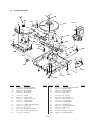
SECTION 8
EXPLODED VIEWS
NOTE:
• -XX and -X mean standardized parts, so they
may have some difference from the original
one.
• Color Indication of Appearance Parts
Example:
KNOB, BALANCE (WHITE) . . . (RED)
↑
↑
Parts Color Cabinet's Color
• Items marked “*” are not stocked since they
are seldom required for routine service. Some
delay should be anticipated when ordering
these items.
(1)
• The mechanical parts with no reference number in the exploded views are not supplied.
• Hardware (# mark) list and accessories and
packing materials are given in the last of the
electrical parts list.
• Abbreviation
AED : North European
AUS : Australian
CND : Canadian
SP : Singapore
The components identified by
mark ! or dotted line with mark
! are critical for safety.
Replace only with part number
specified.
Les composants identifiés par une
marque ! sont critiquens pour la
sécurité.
Ne les remplacer que par une pièce
portant le numéro spécifié.
CASE, FRONT PANEL SECTION
11
10
10
5
10
7
6
5
5
8
#1
5
#1
9
10
5
5
A
4
not supplied
3
#2
2
12
1
Ref. No.
Part No.
Description
Remark
1
2
3
3
4
X-4949-616-1
4-998-523-01
X-4949-618-1
X-4949-619-1
4-996-698-01
DOOR (CD) ASSY
KNOB (JOG)
PANEL ASSY, FRONT (US, CND)
PANEL ASSY, FRONT (EXCEPT US, CND)
EMBLEM, SONY
5
6
4-951-620-01 SCREW (2.6X8), +BVTP
4-985-553-21 CUSHION
Ref. No.
Part No.
Description
* 7
* 7
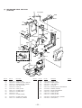
8
* 9
10
A-4724-027-A
A-4724-033-A
1-783-364-11
1-669-161-11
3-363-099-01
DISP BOARD, COMPLETE (US, CND)
DISP BOARD, COMPLETE (EXCEPT US, CND)
WIRE (FLAT TYPE) (15 CORE)
JOG BOARD
SCREW (CASE 3 TP2)
* 11
12
4-982-946-11 CASE
4-977-358-11 CUSHION (FOOT)
– 49 –
Remark
(2)
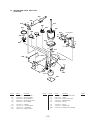
GUIDE ASSY, REAR PANEL SECTION
not supplied
58
59
56
not supplied
#2
55
#2
#2
#3
60
59
57
B
59
59
AUS
#2
#1
AUS
AEP, UK, AED,
SP
71
62
#4 #1
54
#2
#2
#2
59
not
supplied
#1
62
not
supplied
B
63
US, CND
61
#2
#5
53
62
E
#1
62
#4
not
supplied
70 #2
64
66
51
not
supplied
52
#2
67
#2
68
T901
65
69
not
supplied
#2
The components identified by
mark ! or dotted line with
mark ! are critical for safety.
Replace only with part number specified.
Part No.
Description
65
65
65
65
65
4-998-525-01
4-998-525-11
4-998-525-21
4-998-525-41
4-998-525-51
PANEL, BACK (US)
PANEL, BACK (CND)
PANEL, BACK (AEP, UK, AED)
PANEL, BACK (SP)
PANEL, BACK (E)
SHAFT (GUIDE FULCRUM)
SCREW, STEP
GUIDE (DISC T)
CUSHION
CUSHION, SARANET
* 65
* 66
* 66
67
68
4-998-525-61
A-4724-022-A
A-4724-031-A
4-886-821-11
4-053-543-01
PANEL, BACK (AUS)
MAIN BOARD, COMPLETE (US, CND)
MAIN BOARD, COMPLETE (EXCEPT US, CND)
SCREW, S TIGHT, +PTTWH 3X6
RIVET, NYLON
COVER (FFC)
CORD, POWER (US, CND)
CORD, POWER (AEP, UK, AED, SP)
CORD, POWER (E)
CORD, POWER (AUS)
* 69
70
71
! T901
! T901
1-669-164-11
1-773-183-11
4-956-370-12
1-431-759-11
1-431-760-11
JACK BOARD
WIRE (FLAT TYPE) (23 CORE)
BAND, PLUG FIXED (AUS)
TRANSFORMER, POWER (US, CND)
TRANSFORMER, POWER
(AEP, UK, AED, SP, AUS)
! T901
1-431-761-11 TRANSFORMER, POWER (E)
Remark
Ref. No.
Les composants identifiés par une
marque ! sont critiques pour la
sécurité.
Ne les remplacer que par une pièce
portant le numéro spécifié.
Ref. No.
Part No.
Description
* 51
* 52
53
54
* 55
4-982-802-01
4-982-803-01
4-998-506-01
4-999-182-01
1-669-166-11
RING (A)
RING (B)
GUIDE (DOOR. T)
ILLUMINATOR
ILLUMINATION BOARD
*
*
*
*
*
56
57
58
59
* 60
4-982-870-01
3-356-601-11
4-982-862-01
4-985-553-11
3-378-434-01
* 61
! 62
! 62
! 62
! 62
4-982-807-01
1-575-042-21
1-575-651-21
1-696-027-11
1-696-845-11
! 63
* 64
64
1-569-007-11 ADAPTOR, CONVERSION 2P (E)
3-703-244-00 BUSHING (2104), CORD (EXCEPT E)
3-703-571-11 BUSHING (S) (4516), CORD (E)
– 50 –
Remark
(3)
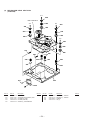
CHASSIS SECTION
#10
#9
118
108
109
#2
110
#2
111
#2
106
117
112
120
#2
107
CDM-40B
119
106
122
#2
112
113
#2
#2
116
103
105 104
#8
#2
121
not
supplied
114
115
124
123
#2
#2
#8
M801
#2
125
102
127
128
#2
#7
126
M810
#2
101
not
supplied
#7
not
supplied
#2
129
130
#5
Ref. No.
Part No.
Description
Ref. No.
Part No.
Description
* 101
* 102
103
104
105
1-669-167-11
X-4949-615-1
4-998-510-01
4-998-509-01
4-998-508-01
DOOR MOTOR BOARD
BRACKET (GEAR) ASSY
GEAR (PULLEY)
GEAR (CENTER)
GEAR (DOOR)
* 117
118
119
120
121
1-661-469-11
4-976-471-01
X-4947-231-1
4-982-892-01
4-982-891-01
D. SENS (RAY CATCHER) BOARD
BEARING (TABLE)
TABLE (200) ASSY
SHAFT (CENTER)
GEAR (TABLE)
106
107
108
* 109
* 110
3-325-697-21
4-998-507-01
4-951-620-01
1-669-168-11
1-661-470-11
WASHER
GUIDE (DOOR.B)
SCREW (2.6X8), +BVTP
DOOR SW BOARD
T. SENS BOARD
122
123
124
* 125
126
4-962-822-01
4-982-893-01
X-4947-607-1
1-661-466-11
3-703-397-01
BELT (TIMING)
GEAR (CENTER 2)
GEAR (PULLEY) ASSY
T. MOTOR BOARD
STOPPER, WIRING
* 111
112
113
114
115
1-661-468-11
3-356-601-11
4-210-030-01
X-4947-230-2
X-4947-606-1
D. SENS (LUMINOUS) BOARD
SCREW, STEP
BELT (42X1)
BRACKET (TABLE) ASSY
HOLDER (ROLLER 2) ASSY
127
128
129
130
M801
4-985-574-01
X-4947-229-1
4-983-279-01
4-931-169-01
A-4604-847-A
SPACER (ROLLER)
HOLDER (ROLLER) ASSY
CUSHION (RF)
FOOT
MOTOR ASSY (TABLE)
M810
X-4950-062-1 DOOR MOTOR ASSY
116
3-701-446-21 WASHER, 8
Remark
– 51 –
Remark
(4)
MECHANISM DECK SECTION-1
(CDM-40B)
#2
not supplied
174
#11
#2
169
#2
161
#2
171
168
173
167
#4
170
162
not supplied
172
160
#1
153 154
not supplied
#4
#13
151
#4
159
152
155
not supplied
166
165
158
#12
156
157
164
163
Ref. No.
Part No.
Description
151
152
153
154
155
X-4947-241-1
4-982-882-01
4-982-881-01
X-4947-239-1
4-982-853-01
LEVER (C) ASSY
SPRING (LIMITTER), TORSION
SPRING (HOLDER), TORSION
LIMITTER (A) ASSY
LEVER (B)
156
157
158
159
160
X-4947-240-1
4-988-143-01
4-982-855-01
4-982-856-01
4-976-458-01
LEVER (A) ASSY
HOLDER (DISC A2)
HOLDER (DISC B)
PAD
HOLDER (MAGNET)
161
162
X-4946-326-1 HOLDER (CLAMP) ASSY
4-983-777-01 SPRING (MG), TENSION
Remark
Ref. No.
Part No.
Description
163
164
165
166
167
A-4672-092-A
3-366-559-02
4-960-633-01
4-960-632-11
4-983-319-01
MAGNET ASSY
MAGNET (CHUCK)
YOKE (MAGNET)
PULLEY (B)
SPRING (THRUST), COMPRESSION
* 168
169
170
171
172
4-976-456-01
3-938-588-01
X-4947-242-1
X-4947-238-1
X-4947-237-1
WASHER (STOPPER)
SPRING, COMPRESSION
SLIDER (C) ASSY
SLIDER (B) ASSY
SLIDER (A) ASSY
173
* 174
4-982-880-01 SPRING (SLIDER A), TENSION
4-982-863-01 GUIDE (DISC P)
– 52 –
Remark
(5)
MECHANISM DECK SECTION-2
(CDM-40B)
212
206
#4
210
213
206
205
201
214
206
206
216
202
203
#2
not supplied
#2
215
204
#2
not supplied
#10
211
209
not supplied
#14
#8
208
M802
207
Part No.
Description
Part No.
Description
201
202
203
204
205
4-976-465-01
4-976-466-01
4-982-893-01
X-4947-607-1
4-982-867-01
GEAR (LOADING 1)
GEAR (LOADING 2)
GEAR (CENTER 2)
GEAR (PULLEY) ASSY
BELT (TIMING)
210
211
212
213
214
X-4947-227-1
4-951-291-01
X-4947-234-1
4-982-857-01
4-982-860-01
LEVER (STOPPER) ASSY
SCREW
SLIDER (LOCK) ASSY
BEARING (CAM)
CAM (A)
206
* 207
* 208
209
3-325-697-21
1-661-465-11
1-661-467-11
3-489-073-00
WASHER
L. MOTOR BOARD
L. SW BOARD
SCREW, THRUST
215
216
M802
4-982-861-01 CAM (B)
3-356-601-11 SCREW, STEP
A-4604-847-A MOTOR ASSY (LOADING)
Ref. No.
Remark
Ref. No.
– 53 –
Remark
(6)
MECHANISM DECK SECTION-3
(CDM-40B)
#15
259
KSM-213BKN/M-N
255
#15
#15
259
259
258
255
255
258
258
#15
259
255
257
255
258
255
256
254
255
254
254
254
253
251
252
#2
Ref. No.
251
252
253
254
255
Part No.
Description
3-356-601-11
X-4947-244-1
X-4947-243-1
4-982-859-01
4-982-878-01
SCREW, STEP
SLIDER (BU ADJUSTMENT) ASSY
HOLDER (BU) ASSY
HOLDER (DAMPER)
SPRING (F), COMPRESSION
Remark
Ref. No.
256
257
258
259
– 54 –
Part No.
Description
4-982-872-01
4-982-871-01
4-982-858-01
4-960-617-01
SPRING (F-2), TENSION
SPRING (F-1), TENSION
DAMPER
CAP (F)
Remark
(7)
OPTICAL PICK-UP SECTION
(KSM-213BKN/M-N)
not supplied
305
306
303
#16
302
M101
304
M102
301
#15
The components identified by
mark ! or dotted line with
mark ! are critical for safety.
Replace only with part number specified.
Ref. No.
Part No.
Description
* 301
302
303
304
A-4724-029-A
2-626-907-01
2-627-003-02
1-769-069-11
BD BOARD, COMPLETE
GEAR (A)
GEAR (B) (RP)
WIRE (FLAT TYPE) (16 CORE)
Remark
Les composants identifiés par une
marque ! sont critiques pour la
sécurité.
Ne les remplacer que par une pièce
portant le numéro spécifié.
Ref. No.
Part No.
Description
305
! 306
M101
M102
2-626-908-01
8-848-379-31
X-2626-234-1
X-2625-769-1
SHAFT, SLED
OPTICAL PICK-UP KSM-213BKN/M-N
T. T CHASSIS ASSY (MG) (K) (SPINDLE)
MOTOR GEAR ASSY (MB) (PP) (SLED)
– 55 –
Remark
SECTION 9
ELECTRICAL PARTS LIST
BD
NOTE:
• Due to standardization, replacements in the
parts list may be different from the parts specified in the diagrams or the components used
on the set.
• -XX and -X mean standardized parts, so they
may have some difference from the original
one.
• RESISTORS
All resistors are in ohms.
METAL: Metal-film resistor.
METAL OXIDE: Metal oxide-film resistor.
F: nonflammable
• Items marked “*” are not stocked since they
are seldom required for routine service.
Some delay should be anticipated when ordering these items.
Ref. No.
Part No.
*
A-4724-029-A BD BOARD, COMPLETE
******************
• SEMICONDUCTORS
In each case, u: µ, for example:
uA. . : µA. .
uPA. . : µPA. .
uPB. . : µPB. .
uPC. . : µPC. .
uPD. . : µPD. .
• CAPACITORS
uF: µF
• COILS
uH: µH
• Abbreviation
AED : North European
AUS : Australian
CND : Canadian
SP : Singapore
Description
Remark
< CAPACITOR >
C101
C102
C103
C104
C106
1-163-005-11
1-163-038-00
1-163-005-11
1-164-232-11
1-164-346-11
CERAMIC CHIP
CERAMIC CHIP
CERAMIC CHIP
CERAMIC CHIP
CERAMIC CHIP
470PF
0.1uF
470PF
0.01uF
1uF
10%
C107
C108
C109
C110
C111
1-164-346-11
1-163-035-00
1-163-145-00
1-163-017-00
1-163-251-11
CERAMIC CHIP
CERAMIC CHIP
CERAMIC CHIP
CERAMIC CHIP
CERAMIC CHIP
1uF
0.047uF
0.0015uF 5%
0.0047uF 5%
100PF
5%
16V
50V
50V
50V
50V
C112
C113
C114
C115
C116
1-163-038-00
1-163-038-00
1-163-038-00
1-126-607-11
1-126-607-11
CERAMIC CHIP
CERAMIC CHIP
CERAMIC CHIP
ELECT CHIP
ELECT CHIP
0.1uF
0.1uF
0.1uF
47uF
47uF
25V
25V
25V
4V
4V
C117
C118
C119
C120
C121
1-126-209-11
1-163-275-11
1-163-231-11
1-163-038-00
1-163-038-00
ELECT CHIP
CERAMIC CHIP
CERAMIC CHIP
CERAMIC CHIP
CERAMIC CHIP
100uF
0.001uF
15PF
0.1uF
0.1uF
20%
5%
5%
C122
C123
C124
C125
C126
1-135-155-21
1-164-232-11
1-164-005-11
1-163-038-00
1-163-038-00
TANTALUM CHIP
CERAMIC CHIP
CERAMIC CHIP
CERAMIC CHIP
CERAMIC CHIP
4.7uF
0.01uF
0.47uF
0.1uF
0.1uF
10%
C127
C130
C131
C140
C141
1-109-982-11
1-164-004-11
1-135-216-11
1-163-038-00
1-163-038-00
CERAMIC CHIP
CERAMIC CHIP
TANTALUM CHIP
CERAMIC CHIP
CERAMIC CHIP
1uF
0.1uF
10uF
0.1uF
0.1uF
10%
10%
20%
C151
C153
C154
C156
C157
1-163-237-11
1-163-038-00
1-164-336-11
1-163-237-11
1-163-145-00
CERAMIC CHIP
CERAMIC CHIP
CERAMIC CHIP
CERAMIC CHIP
CERAMIC CHIP
C159
C161
C162
1-163-019-00 CERAMIC CHIP
1-126-205-11 ELECT CHIP
1-126-205-11 ELECT CHIP
10%
20%
20%
50V
25V
50V
50V
16V
4V
50V
50V
25V
25V
Ref. No.
Part No.
The components identified by
mark ! or dotted line with mark
! are critical for safety.
Replace only with part number
specified.
Les composants identifiés par une
marque ! sont critiquens pour la
sécurité.
Ne les remplacer que par une pièce
portant le numéro spécifié.
When indicating parts by reference
number, please include the board.
Description
Remark
C163
C164
1-126-205-11 ELECT CHIP
1-163-038-00 CERAMIC CHIP
47uF
0.1uF
20%
6.3V
25V
C165
C166
C167
C168
C171
1-163-038-00
1-163-038-00
1-163-235-11
1-163-237-11
1-163-137-00
CERAMIC CHIP
CERAMIC CHIP
CERAMIC CHIP
CERAMIC CHIP
CERAMIC CHIP
0.1uF
0.1uF
22PF
27PF
680PF
5%
5%
5%
25V
25V
50V
50V
50V
C172
C181
C182
1-163-251-11 CERAMIC CHIP
1-163-137-00 CERAMIC CHIP
1-163-251-11 CERAMIC CHIP
100PF
680PF
100PF
5%
5%
5%
50V
50V
50V
< CONNECTOR >
CN101
CN102
1-770-072-11 CONNECTOR, (LIF (NON-ZIF)) FFC23P
1-777-937-11 CONNECTOR, FFC/FPC 16P
< IC >
IC101
IC102
IC103
8-752-386-85 IC CXD2587Q
8-759-455-91 IC BA6392FP-E2
8-752-085-51 IC CXA2568M-T6
< COIL >
L101
L102
1-414-234-11 INDUCTOR CHIP 0uH
1-414-234-11 INDUCTOR CHIP 0uH
< TRANSISTOR >
16V
50V
25V
25V
25V
Q101
10V
25V
10V
25V
25V
R101
R102
R103
R104
R105
1-216-077-00
1-216-097-00
1-216-077-00
1-216-085-00
1-216-097-00
METAL CHIP
RES, CHIP
METAL CHIP
METAL CHIP
RES, CHIP
15K
100K
15K
33K
100K
5%
5%
5%
5%
5%
1/10W
1/10W
1/10W
1/10W
1/10W
27PF
5%
0.1uF
0.33uF
27PF
5%
0.0015uF 5%
50V
25V
25V
50V
50V
R106
R107
R108
R109
R110
1-216-061-00
1-216-061-00
1-216-073-00
1-216-121-00
1-216-025-00
METAL CHIP
METAL CHIP
METAL CHIP
RES, CHIP
RES, CHIP
3.3K
3.3K
10K
1M
100
5%
5%
5%
5%
5%
1/10W
1/10W
1/10W
1/10W
1/10W
0.0068uF 10%
47uF
20%
47uF
20%
50V
6.3V
6.3V
R111
R113
R116
1-216-121-00 RES, CHIP
1-216-121-00 RES, CHIP
1-216-025-00 RES, CHIP
1M
1M
100
5%
5%
5%
1/10W
1/10W
1/10W
8-729-010-08 TRANSISTOR MSB710-R
< RESISTOR >
– 56 –
BD
Ref. No.
Part No.
D. SENS (LUMINOUS)
Description
Remark
R117
R119
1-216-049-11 RES, CHIP
1-216-043-00 RES, CHIP
1K
560
5%
5%
1/10W
1/10W
R123
R124
R131
R135
R136
1-216-073-00
1-216-097-00
1-216-037-00
1-216-295-00
1-216-295-00
METAL CHIP
RES, CHIP
METAL CHIP
SHORT
SHORT
10K
100K
330
0
0
5%
5%
5%
1/10W
1/10W
1/10W
R137
R138
R143
R144
R147
1-216-295-00
1-216-295-00
1-216-103-00
1-216-103-00
1-216-081-00
SHORT
SHORT
METAL CHIP
METAL CHIP
METAL CHIP
0
0
180K
180K
22K
5%
5%
5%
1/10W
1/10W
1/10W
R148
R149
R158
R159
R161
1-216-001-00
1-216-003-11
1-216-111-00
1-216-101-00
1-216-308-00
METAL CHIP
RES, CHIP
METAL CHIP
METAL CHIP
METAL CHIP
10
12
390K
150K
4.7
5%
5%
5%
5%
5%
1/10W
1/10W
1/10W
1/10W
1/10W
R162
R171
R172
R173
R181
1-216-101-00
1-216-077-00
1-216-077-00
1-216-077-00
1-216-077-00
METAL CHIP
METAL CHIP
METAL CHIP
METAL CHIP
METAL CHIP
150K
15K
15K
15K
15K
5%
5%
5%
5%
5%
1/10W
1/10W
1/10W
1/10W
1/10W
R182
R183
1-216-077-00 METAL CHIP
1-216-077-00 METAL CHIP
15K
15K
5%
5%
1/10W
1/10W
Ref. No.
D. SENS (RAY CATCHER)
Part No.
0.01uF
0.1uF
100uF
20%
20%
16V
50V
10V
C706
C707
C708
C709
C710
1-162-282-31
1-162-282-31
1-162-282-31
1-162-288-31
1-124-584-00
100PF
100PF
100PF
330PF
100uF
10%
10%
10%
10%
20%
50V
50V
50V
50V
10V
C711
C712
1-164-159-11 CERAMIC
1-164-159-11 CERAMIC
< LED >
D701
D702
D703
D704
D705
8-719-046-39
8-719-046-39
8-719-046-39
8-719-046-39
8-719-046-39
LED
LED
LED
LED
LED
SEL5821A-TH15 (GROUP 1)
SEL5821A-TH15 (GROUP 2)
SEL5821A-TH15 (GROUP 3)
SEL5821A-TH15 (GROUP 4)
SEL5821A-TH15 (GROUP 5)
D706
D707
D708
D709
8-719-046-39
8-719-046-39
8-719-046-39
8-719-046-44
LED
LED
LED
LED
SEL5821A-TH15 (GROUP 6)
SEL5821A-TH15 (GROUP 7)
SEL5821A-TH15 (GROUP 8)
SEL5221S (STANDBY)
1-517-756-11 INDICATOR TUBE, FLUORESCENT
< IC >
IC601
IC701
IC702
8-749-014-66 IC NJL56H400
8-759-498-92 IC MSM9202-03GS-K
8-759-183-47 IC M66310FP
< TRANSISTOR >
Q701
8-729-900-80 TRANSISTOR DTC114ES
< DIODE >
< RESISTOR >
D801
8-719-055-84 DIODE GL-528VS1
************************************************************
*
1-661-469-11 D.SENS (RAY CATCHER) BOARD
**************************
4-985-300-01 HOLDER (P-T)
< PHOTO TRANSISTOR >
Q801
8-729-926-31 PHOTO TRANSISTOR PT483F1S
************************************************************
*
*
A-4724-027-A DISP BOARD, COMPLETE (US, CND)
A-4724-033-A DISP BOARD, COMPLETE (EXCEPT US, CND)
********************
*
4-982-811-01 HOLDER (FL)
< CAPACITOR >
1-162-294-31 CERAMIC
1-162-215-31 CERAMIC
50V
50V
* CLP701 1-690-880-31 LEAD (WITH CONNECTOR)
FL701
1-572-085-11 SWITCH, LEAF (LIMIT)
4-976-473-01 HOLDER (LED-S)
C701
C702
0.1uF
0.1uF
< LEAD PIN >
1-661-468-11 D.SENS (LUMINOUS) BOARD
***********************
*
CERAMIC
CERAMIC
CERAMIC
CERAMIC
ELECT
< FLUORESCENT INDICATOR TUBE >
X101
1-767-408-41 VIBRATOR, CRYSTAL (16.9344MHz)
************************************************************
*
Remark
1-162-306-11 CERAMIC
1-164-159-11 CERAMIC
1-124-584-00 ELECT
< VIBRATOR >
*
Description
C703
C704
C705
< SWITCH >
S101
DISP
0.001uF
47PF
10%
5%
50V
50V
R701
R702
R703
R704
R705
1-249-441-11
1-247-807-31
1-247-807-31
1-247-807-31
1-247-807-31
CARBON
CARBON
CARBON
CARBON
CARBON
100K
100
100
100
100
5%
5%
5%
5%
5%
1/4W
1/4W
1/4W
1/4W
1/4W
R706
R707
R708
R709
R711
1-247-843-11
1-247-807-31
1-247-807-31
1-247-807-31
1-249-411-11
CARBON
CARBON
CARBON
CARBON
CARBON
3.3K
100
100
100
330
5%
5%
5%
5%
5%
1/4W
1/4W
1/4W
1/4W
1/4W
R712
R713
R722
R723
R724
1-249-411-11
1-249-413-11
1-249-415-11
1-249-417-11
1-249-419-11
CARBON
CARBON
CARBON
CARBON
CARBON
330
470
680
1K
1.5K
5%
5%
5%
5%
5%
1/4W
1/4W
1/4W
1/4W
1/4W
R725
R726
R727
R728
R732
1-249-421-11
1-247-843-11
1-249-427-11
1-249-431-11
1-249-415-11
CARBON
CARBON
CARBON
CARBON
CARBON
2.2K
3.3K
6.8K
15K
680
5%
5%
5%
5%
5%
1/4W
1/4W
1/4W
1/4W
1/4W
– 57 –
DISP
Ref. No.
DOOR MOTOR
Part No.
DOOR SW
Description
ILLUMINATION
Remark
R733
R734
R735
R736
R737
1-249-417-11
1-249-419-11
1-249-421-11
1-247-843-11
1-249-427-11
CARBON
CARBON
CARBON
CARBON
CARBON
1K
1.5K
2.2K
3.3K
6.8K
5%
5%
5%
5%
5%
1/4W
1/4W
1/4W
1/4W
1/4W
R751
1-249-429-11 CARBON
10K
5%
1/4W
1-572-184-11
1-572-184-11
1-572-184-11
1-572-184-11
1-572-184-11
SWITCH, KEYBOARD (REPEAT)
SWITCH, KEYBOARD (PROGRAM)
SWITCH, KEYBOARD (SHUFFLE)
SWITCH, KEYBOARD (CONTINUE)
SWITCH, KEYBOARD (GROUP 4)
S726
S727
S728
S731
S732
1-572-184-11
1-572-184-11
1-572-184-11
1-572-184-11
1-572-184-11
SWITCH, KEYBOARD (GROUP 3)
SWITCH, KEYBOARD (GROUP 2)
SWITCH, KEYBOARD (GROUP 1)
SWITCH, KEYBOARD (I/u)
SWITCH, KEYBOARD (TIME/TEXT)
Ref. No.
Part No.
*
1-669-164-11 JACK BOARD
**********
Description
Remark
*
4-962-200-11 PLATE (TR), GROUND
< CAPACITOR >
< SWITCH >
S721
S722
S723
S724
S725
JACK
C351
C451
C901
C904
C907
1-162-290-31
1-162-290-31
1-161-494-00
1-164-159-11
1-164-159-11
CERAMIC
CERAMIC
CERAMIC
CERAMIC
CERAMIC
470PF
470PF
0.022uF
0.1uF
0.1uF
C911
C912
1-161-494-00 CERAMIC
1-126-052-11 ELECT
0.022uF
100uF
10%
10%
20%
50V
50V
25V
50V
50V
25V
10V
< CONNECTOR >
CN902
* CN903
* CN904
CN906
S733
1-572-184-11 SWITCH, KEYBOARD (GROUP FILE)
S734
1-572-184-11 SWITCH, KEYBOARD (GROUP 8)
S735
1-572-184-11 SWITCH, KEYBOARD (GROUP 7)
S736
1-572-184-11 SWITCH, KEYBOARD (GROUP 6)
S737
1-572-184-11 SWITCH, KEYBOARD (GROUP 5)
************************************************************
1-569-497-11
1-569-496-11
1-568-951-11
1-580-230-11
< DIODE >
D901
8-719-911-19 DIODE 1SS119
< IC >
IC901
8-749-921-12 IC GP1F32T (DIGITAL OUT OPTICAL)
1-669-167-11 DOOR MOTOR BOARD
******************
*
< JACK >
< CONNECTOR >
* J901
* CN812 1-568-951-11 PIN, CONNECTOR 2P
************************************************************
1-669-168-11 DOOR SW BOARD
**************
*
SOCKET, CONNECTOR 11P
SOCKET, CONNECTOR 10P
PIN, CONNECTOR 2P
PIN, CONNECTOR (PC BOARD) 2P
* J902
J904
1-764-188-11 JACK (SMALL TYPE) (DIA. 3.5)
(S-LINK CONTROL A1)
1-764-188-11 JACK (SMALL TYPE) (DIA. 3.5)
(S-LINK CONTROL A1)
1-770-719-11 JACK, PIN 2P (LINE OUT)
< LINE FILTER >
< RESISTOR >
! L901
R807
1-249-429-11 CARBON
10K
5%
1-421-915-11 FILTER, LINE (EXCEPT E)
1/4W
< COIL >
< SWITCH >
L902
1-410-503-11 INDUCTOR
S810
1-571-300-21 SWITCH, ROTARY (DOOR SW)
************************************************************
1-669-166-11 ILLUMINATION BOARD
******************
*
3.3uH
< TRANSISTOR >
Q901
8-729-620-05 TRANSISTOR 2SC2603-EF
< RESISTOR >
< CONNECTOR >
CN813
1-506-481-11 PIN, CONNECTOR 2P
< LED >
D802
D803
D804
8-719-059-65 LED HLMF-KL05 (INSIDE ILLUMINATION)
8-719-059-65 LED HLMF-KL05 (INSIDE ILLUMINATION)
8-719-059-65 LED HLMF-KL05 (INSIDE ILLUMINATION)
R351
R451
R901
R902
R903
1-215-405-00
1-215-405-00
1-249-393-11
1-249-425-11
1-249-429-11
METAL
METAL
CARBON
CARBON
CARBON
220
220
10
4.7K
10K
1%
1%
5%
5%
5%
1/4W
1/4W
1/4W
1/4W
1/4W
R921
1-249-429-11 CARBON
10K
5%
1/4W
< SWITCH >
< RESISTOR >
R805
1-249-407-11 CARBON
150
5%
1/4W
R806
1-249-401-11 CARBON
47
5%
1/4W
************************************************************
S901
! S902
– 58 –
1-762-910-11 SWITCH, SLIDE (COMMAND MODE)
1-572-675-11 SWITCH, POWER VOLTAGE CHANGE
(VOLTAGE SELECTOR) (E)
The components identified by
mark ! or dotted line with
mark ! are critical for safety.
Replace only with part number specified.
Les composants identifiés par une
marque ! sont critiques pour la
sécurité.
Ne les remplacer que par une pièce
portant le numéro spécifié.
JACK
Ref. No.
Part No.
Description
Remark
< TRANSFORMER >
1-431-759-11 TRANSFORMER, POWER (US, CND)
1-431-760-11 TRANSFORMER, POWER
(AEP, AED, UK, SP, AUS)
! T901
1-431-761-11 TRANSFORMER, POWER (E)
************************************************************
JOG
L.MOTOR
Ref. No.
Part No.
*
1-661-467-11 L.SW BOARD
**********
! T901
! T901
1-669-161-11 JOG BOARD
**********
*
L.SW
Description
MAIN
Remark
< SWITCH >
S801
1-571-300-21 SWITCH, ROTARY (LOADING DET)
************************************************************
A-4724-022-A MAIN BOARD, COMPLETE (US, CND)
A-4724-031-A MAIN BOARD, COMPLETE (EXCEPT US, CND)
*********************
*
*
< CONNECTOR >
7-685-871-01 SCREW +BVTT 3X6 (S)
* CN601
1-569-306-11 SOCKET, CONNECTOR (L TYRE) 15P
< CAPACITOR >
< LED >
D601
D602
8-719-046-40 LED SEL5521C-TH8F (·)
8-719-046-38 LED SEL5821A-TH8F (P)
< RESISTOR >
1-126-233-11
1-126-052-11
1-126-163-11
1-126-233-11
1-126-052-11
ELECT
ELECT
ELECT
ELECT
ELECT
22uF
100uF
4.7uF
22uF
100uF
20%
20%
20%
20%
20%
20%
20%
50V
10V
50V
50V
10V
R601
R602
R612
R613
R614
1-249-407-11
1-249-409-11
1-249-415-11
1-249-417-11
1-249-419-11
CARBON
CARBON
CARBON
CARBON
CARBON
150
220
680
1K
1.5K
5%
5%
5%
5%
5%
1/4W
1/4W
1/4W
1/4W
1/4W
C501
C502
1-128-489-11 ELECT
1-124-360-00 ELECT
3300uF
1000uF
C502
1-126-027-11 ELECT
1000uF
R615
R616
R617
R618
R619
1-249-421-11
1-247-843-11
1-249-427-11
1-249-431-11
1-249-437-11
CARBON
CARBON
CARBON
CARBON
CARBON
2.2K
3.3K
6.8K
15K
47K
5%
5%
5%
5%
5%
1/4W
1/4W
1/4W
1/4W
1/4W
C503
C504
C505
C506
C507
1-124-122-11
1-126-021-11
1-126-052-11
1-126-101-11
1-126-044-11
ELECT
ELECT
ELECT
ELECT
ELECT
100uF
33uF
100uF
100uF
1uF
20%
20%
20%
20%
20%
50V
35V
16V
16V
50V
R622
R623
R624
R651
R652
1-249-415-11
1-249-417-11
1-249-419-11
1-249-429-11
1-249-429-11
CARBON
CARBON
CARBON
CARBON
CARBON
680
1K
1.5K
10K
10K
5%
5%
5%
5%
5%
1/4W
1/4W
1/4W
1/4W
1/4W
C508
C509
C510
C511
C512
1-126-101-11
1-124-997-11
1-126-163-11
1-126-163-11
1-161-494-00
ELECT
ELECT
ELECT
ELECT
CERAMIC
100uF
470uF
4.7uF
4.7uF
0.022uF
20%
20%
20%
20%
16V
10V
50V
50V
25V
C513
C514
C516
C518
1-126-052-11
1-126-023-11
1-164-159-11
1-164-159-11
ELECT
ELECT
CERAMIC
CERAMIC
100uF
100uF
0.1uF
0.1uF
20%
20%
16V
25V
50V
50V
C519
C521
C522
C531
C532
1-164-159-11
1-164-159-11
1-110-489-11
1-161-494-00
1-126-052-11
CERAMIC
CERAMIC
CAPACITOR
CERAMIC
ELECT
0.1uF
0.1uF
1F
0.022uF
100uF
C533
C551
C552
C561
C562
1-161-494-00
1-136-165-00
1-164-159-11
1-136-165-00
1-164-159-11
CERAMIC
FILM
CERAMIC
FILM
CERAMIC
0.022uF
0.1uF
0.1uF
0.1uF
0.1uF
C571
C572
C610
C620
C720
1-136-165-00
1-164-159-11
1-161-494-00
1-161-494-00
1-161-494-00
FILM
CERAMIC
CERAMIC
CERAMIC
CERAMIC
0.1uF
0.1uF
0.022uF
0.022uF
0.022uF
C730
1-161-494-00 CERAMIC
0.022uF
< ROTARY ENCODER >
RE601
1-475-543-11 ENCODER, ROTARY
(DISC/CHARACTER PUSH ENTER)
< SWITCH >
S611
S612
S613
S614
S615
1-572-184-11
1-572-184-11
1-572-184-11
1-572-184-11
1-572-184-11
SWITCH, KEYBOARD (p)
SWITCH, KEYBOARD (P)
SWITCH, KEYBOARD (·)
SWITCH, KEYBOARD (CLEAR)
SWITCH, KEYBOARD (CHECK)
S616
1-572-184-11 SWITCH, KEYBOARD (±, AMS)
S617
1-572-184-11 SWITCH, KEYBOARD (≠, AMS)
S621
1-572-184-11 SWITCH, KEYBOARD (§, OPEN/CLOSE)
S622
1-572-184-11 SWITCH, KEYBOARD (INPUT)
S623
1-572-184-11 SWITCH, KEYBOARD (MEMO SEARCH)
************************************************************
*
C301
C305
C327
C401
C405
1-661-465-11 L.MOTOR BOARD
**************
************************************************************
16V
16V
(US, CND)
20%
25V
(EXCEPT US, CND)
20%
5%
5%
5%
50V
50V
5.5V
25V
10V
25V
50V
50V
50V
50V
50V
50V
25V
25V
25V
25V
< CONNECTOR >
CN501
CN502
– 59 –
1-569-321-11 SOCKET, CONNECTOR 15P
1-568-742-11 SOCKET, CONNECTOR 23P
The components identified by
mark ! or dotted line with
mark ! are critical for safety.
Replace only with part number specified.
Les composants identifiés par une
marque ! sont critiques pour la
sécurité.
Ne les remplacer que par une pièce
portant le numéro spécifié.
MAIN
Ref. No.
Part No.
* CN503
CN504
CN505
1-568-951-11 PIN, CONNECTOR 2P
1-506-469-11 PIN, CONNECTOR 4P
1-506-468-11 PIN, CONNECTOR 3P
*
*
*
*
CN506
CN507
CN508
CN509
1-568-955-11
1-568-951-11
1-569-505-11
1-569-506-11
Description
Remark
PIN, CONNECTOR 6P
PIN, CONNECTOR 2P
PIN, CONNECTOR 10P
PIN, CONNECTOR 11P
< DIODE >
D327
D501
D502
D503
D504
8-719-911-19
8-719-024-99
8-719-024-99
8-719-024-99
8-719-024-99
DIODE
DIODE
DIODE
DIODE
DIODE
1SS119
11ES2-NTA2B
11ES2-NTA2B
11ES2-NTA2B
11ES2-NTA2B
D505
D506
D507
D508
D509
8-719-024-99
8-719-110-72
8-719-109-93
8-719-109-85
8-719-911-19
DIODE
DIODE
DIODE
DIODE
DIODE
11ES2-NTA2B
RD30ESB2
RD6.2ESB2
RD5.1ES-B2
1SS119
D521
8-719-911-19 DIODE 1SS119
< IC >
IC401
IC501
IC502
IC503
IC504
8-759-145-58
8-752-892-41
8-759-463-99
8-759-821-32
8-759-094-53
IC
IC
IC
IC
IC
uPC4558C
CXP84340-075Q
M5M5256DFP-70XL
CXA1291P
TA7805S
IC505
IC506
8-759-256-72 IC PST994D
8-759-330-29 IC LA5616
< COIL >
L501
L502
1-412-473-21 INDUCTOR
1-412-473-21 INDUCTOR
0uH
0uH
Ref. No.
Part No.
Description
R323
R325
R327
R401
R402
1-249-421-11
1-249-441-11
1-249-441-11
1-215-453-00
1-215-425-00
CARBON
CARBON
CARBON
METAL
METAL
2.2K
100K
100K
22K
1.5K
5%
5%
5%
1%
1%
1/4W
1/4W
1/4W
1/4W
1/4W
Remark
R403
R404
R405
R413
R414
1-215-425-00
1-215-445-00
1-215-443-00
1-215-469-00
1-215-405-00
METAL
METAL
METAL
METAL
METAL
1.5K
10K
8.2K
100K
220
1%
1%
1%
1%
1%
1/4W
1/4W
1/4W
1/4W
1/4W
R415
R416
R422
R423
R425
1-215-405-00
1-249-393-11
1-249-421-11
1-249-421-11
1-249-441-11
METAL
CARBON
CARBON
CARBON
CARBON
220
10
2.2K
2.2K
100K
1%
5%
5%
5%
5%
1/4W
1/4W
1/4W
1/4W
1/4W
R501
R502
R505
R506
R507
1-249-435-11
1-249-425-11
1-249-413-11
1-249-429-11
1-249-425-11
CARBON
CARBON
CARBON
CARBON
CARBON
33K
4.7K
470
10K
4.7K
5%
5%
5%
5%
5%
1/4W
1/4W
1/4W
1/4W
1/4W
R508
R511
R512
R521
R522
1-249-413-11
1-249-425-11
1-249-425-11
1-249-429-11
1-249-403-11
CARBON
CARBON
CARBON
CARBON
CARBON
470
4.7K
4.7K
10K
68
5%
5%
5%
5%
5%
1/4W
1/4W
1/4W
1/4W
1/4W
R523
R524
R531
R532
R533
1-249-403-11
1-249-429-11
1-249-429-11
1-249-429-11
1-249-429-11
CARBON
CARBON
CARBON
CARBON
CARBON
68
10K
10K
10K
10K
5%
5%
5%
5%
5%
1/4W
1/4W
1/4W
1/4W
1/4W
R534
R535
R536
R537
R538
1-249-421-11
1-247-843-11
1-249-425-11
1-249-429-11
1-249-429-11
CARBON
CARBON
CARBON
CARBON
CARBON
2.2K
3.3K
4.7K
10K
10K
5%
5%
5%
5%
5%
1/4W
1/4W
1/4W
1/4W
1/4W
R539
R540
R541
R542
R543
1-249-429-11
1-249-429-11
1-249-429-11
1-249-429-11
1-249-429-11
CARBON
CARBON
CARBON
CARBON
CARBON
10K
10K
10K
10K
10K
5%
5%
5%
5%
5%
1/4W
1/4W
1/4W
1/4W
1/4W
R544
R551
R552
R553
R554
1-249-429-11
1-247-887-00
1-247-887-00
1-247-860-11
1-249-431-11
CARBON
CARBON
CARBON
CARBON
CARBON
10K
220K
220K
16K
15K
5%
5%
5%
5%
5%
1/4W
1/4W
1/4W
1/4W
1/4W
R555
R556
R557
R558
R561
1-249-382-11
1-249-382-11
1-247-883-00
1-249-393-11
1-249-441-11
CARBON
CARBON
CARBON
CARBON
CARBON
1.2
1.2
150K
10
100K
5%
5%
5%
5%
5%
1/6W
1/6W
1/4W
1/4W
1/4W
R562
R563
R564
R565
R566
1-249-441-11
1-247-860-11
1-249-431-11
1-249-382-11
1-249-382-11
CARBON
CARBON
CARBON
CARBON
CARBON
100K
16K
15K
1.2
1.2
5%
5%
5%
5%
5%
1/4W
1/4W
1/4W
1/6W
1/6W
R567
R568
R571
1-247-883-00 CARBON
1-249-393-11 CARBON
1-247-885-00 CARBON
150K
10
180K
5%
5%
5%
1/4W
1/4W
1/4W
< TRANSISTOR >
Q322
Q323
Q325
Q327
Q422
8-729-141-26
8-729-141-26
8-729-900-65
8-729-900-65
8-729-141-26
TRANSISTOR
TRANSISTOR
TRANSISTOR
TRANSISTOR
TRANSISTOR
2SC3622A-LK
2SC3622A-LK
DTA144ES
DTA144ES
2SC3622A-LK
Q423
Q425
Q501
Q503
Q521
8-729-141-26
8-729-900-65
8-729-140-97
8-729-119-76
8-729-030-08
TRANSISTOR
TRANSISTOR
TRANSISTOR
TRANSISTOR
TRANSISTOR
2SC3622A-LK
DTA144ES
2SB734-34
2SA1175-HFE
DTC144VSA-TP
< RESISTOR >
R301
R302
R303
R304
R305
1-215-453-00
1-215-425-00
1-215-425-00
1-215-445-00
1-215-443-00
METAL
METAL
METAL
METAL
METAL
22K
1.5K
1.5K
10K
8.2K
1%
1%
1%
1%
1%
1/4W
1/4W
1/4W
1/4W
1/4W
R313
R314
R315
R316
R322
1-215-469-00
1-215-405-00
1-215-405-00
1-249-393-11
1-249-421-11
METAL
METAL
METAL
CARBON
CARBON
100K
220
220
10
2.2K
1%
1%
1%
5%
5%
1/4W
1/4W
1/4W
1/4W
1/4W
– 60 –
MAIN
T.MOTOR
T.SENS
Remark
Ref. No.
Part No.
R572
R573
1-247-885-00 CARBON
1-247-860-11 CARBON
180K
16K
5%
5%
1/4W
1/4W
M810
! T901
X-4950-062-1 DOOR MOTOR ASSY
1-431-759-11 TRANSFORMER, POWER (US, CND)
R574
R575
R576
R577
R578
1-249-431-11
1-249-382-11
1-249-382-11
1-247-883-00
1-249-393-11
CARBON
CARBON
CARBON
CARBON
CARBON
15K
1.2
1.2
150K
10
5%
5%
5%
5%
5%
1/4W
1/6W
1/6W
1/4W
1/4W
! T901
R581
R610
R620
R720
R730
1-249-429-11
1-249-427-11
1-249-427-11
1-249-427-11
1-249-427-11
CARBON
CARBON
CARBON
CARBON
CARBON
10K
6.8K
6.8K
6.8K
6.8K
5%
5%
5%
5%
5%
1/4W
1/4W
1/4W
1/4W
1/4W
Ref. No.
Part No.
Description
**************
HARDWARE LIST
**************
X501
1-579-175-11 VIBRATOR, CERAMIC (10MHz)
************************************************************
1-661-466-11 T.MOTOR BOARD
*************
************************************************************
1-661-470-11 T.SENS BOARD
************
*
#1
#2
#3
#4
#5
7-685-646-79
7-685-871-01
7-685-134-19
7-624-106-04
7-682-947-01
SCREW +BVTP 3X8 TYPE2 N-S
SCREW +BVTT 3X6 (S)
SCREW +PTPWH 2.6X8 (TYPE2)
STOP RING 3.0, TYPE -E
SCREW +PSW 3X6
#6
#7
#8
#9
#10
7-682-547-04
7-685-872-09
7-621-775-00
7-685-647-79
7-624-111-04
SCREW +BV 3X6, S TIGHT
SCREW +BVTT 3X8 (S)
SCREW +B 2.6X3
SCREW +BVTP 3X10 TYPE2 N-S
STOP RING 7.0, TYPE -E
#11
#12
#13
#14
#15
7-682-552-09
7-621-772-20
7-624-109-04
7-621-775-20
7-621-772-30
SCREW +B 3X16
SCREW +B 2X5
STOP RING 5.0, TYPE -E
SCREW +B 2.6X5
SCREW +B 2X6
1-241-787-11 RES, ADJ, CARBON 47K
< VIBRATOR >
*
Remark
1-431-760-11 TRANSFORMER, POWER
(AEP, UK, AED, SP, AUS)
! T901
1-431-761-11 TRANSFORMER, POWER (E)
************************************************************
< VARIABLE RESISTOR >
RV501
Description
#16
7-621-255-15 SCREW +P 2X3
************************************************************
< CONNECTOR >
CN802
CN803
ACCESSORIES & PACKING MATERIALS
*******************************
1-506-481-11 PIN, CONNECTOR 2P
1-506-481-11 PIN, CONNECTOR 2P
1-475-654-11 REMOTE COMMANDER (RM-DX220)
1-558-271-11 CORD, CONNECTION (AUDIO) 1.5m
1-777-172-11 CORD, CONNECTION (CONTROL A1) 1m
< PHOTO INTERRUPTER >
IC801
IC802
IC803
8-749-924-18 PHOTO INTERRUPTER RPI-1391
8-749-924-18 PHOTO INTERRUPTER RPI-1391
8-749-924-18 PHOTO INTERRUPTER RPI-1391
< RESISTOR >
R801
1-249-416-11 CARBON
820
5%
1/4W
R802
1-249-416-11 CARBON
820
5%
1/4W
R803
1-249-416-11 CARBON
820
5%
1/4W
R804
1-249-415-11 CARBON
680
5%
1/4W
************************************************************
MISCELLANEOUS
**************
8
! 62
! 62
! 62
! 62
1-783-364-11
1-575-042-21
1-575-651-21
1-696-027-11
1-696-845-11
WIRE (FLAT TYPE) (15 CORE)
CORD, POWER (US, CND)
CORD, POWER (AEP, UK, AED, SP)
CORD, POWER (E)
CORD, POWER (AUS)
! 63
70
304
! 306
M101
1-569-007-11
1-773-183-11
1-769-069-11
8-848-379-31
X-2626-234-1
ADAPTOR, CONVERSION 2P (E)
WIRE (FLAT TYPE) (23 CORE)
WIRE (FLAT TYPE) (16 CORE)
OPTICAL PICK-UP KSM-213BKN/M-N
T. T CHASSIS ASSY (MG) (K) (SPINDLE)
M102
M801
M802
(CND)
3-810-765-11 MANUAL, COMMONNESS INSTRUCTION
(ENGLISH) (US, AUS)
3-810-765-21 MANUAL, COMMONNESS INSTRUCTION
(ENGLISH, FRENCH, GERMAN, SPANISH,
DUTCH, SWEDISH, ITALIAN, PORTUGUESE,
CHINESE) (CND, AEP, UK, AED, E, SP)
3-862-563-11 MANUAL, INSTRUCTION (ENGLISH) (US, AUS)
3-862-563-21 MANUAL, INSTRUCTION (ENGLISH, FRENCH,
SPANISH) (CND, AEP, UK, E, SP)
3-862-563-31 MANUAL, INSTRUCTION (GERMAN, DUTCH,
ITALIAN, PORTUGUESE) (AEP, UK)
3-862-563-41 MANUAL, INSTRUCTION
(SWEDISH, DANISH, FINNISH) (AED)
3-862-563-51 MANUAL, INSTRUCTION (CHINESE) (E, SP)
4-981-643-01 COVER, BATTERY (for RM-DX220)
4-984-086-01 BOOKLET (100)
X-2625-769-1 MOTOR GEAR ASSY (MB) (PP) (SLED)
A-4604-847-A MOTOR ASSY (TABLE)
A-4604-847-A MOTOR ASSY (LOADING)
– 61 –
The components identified by
mark ! or dotted line with
mark ! are critical for safety.
Replace only with part number specified.
Les composants identifiés par une
marque ! sont critiques pour la
sécurité.
Ne les remplacer que par une pièce
portant le numéro spécifié.
CDP-CX220
Sony Corporation
9-922-819-11
Home A&V Products Company
– 62 –
98D0589-1
Printed in Japan © 1998. 4
Published by Quality Assurance Dept.
(Shibaura)