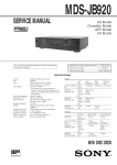
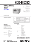
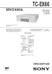
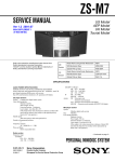
1
MDS-EX77 SERVICE MANUAL AEP Model UK Model E Model MDS-EX77 is the mini disc deck section in DHC-MD77/EX77MD. U.S and foreign patents licensed from Dolby Laboratories Licensing Corporation. Model Name Using Similar Mechanism MDS-S37 MD Mechanism Type MDM-3A Optical Pick-up Name KMS-260A/J1N SPECIFICATIONS MINI DISC DECK MICROFILM TABLE OF CONTENTS 1. NOTES ON HANDLING THE OPTICAL PICK-UP BLOCK OR BASE UNIT SERVICING NOTES 2. GENERAL .................................................................. 7 3. DISASSEMBLY ........................................................ 19 The laser diode in the optical pick-up block may suffer electrostatic break-down because of the potential difference generated by the charged electrostatic load, etc. on clothing and the human body. During repair, pay attention to electrostatic break-down and also use the procedure in the printed matter which is included in the repair parts. The flexible board is easily damaged and should be handled with care. 4. TEST MODE NOTES ON LASER DIODE EMISSION CHECK 4-1. 4-2. 4-3. 4-4. 4-5. 4-6. 4-7. 4-8. 4-9. 4-10. 4-11. Precautions for Use of Test Mode .................................. Setting the Test Mode ..................................................... Releasing the Test Mode ................................................ Basic Operations of the Test Mode ................................ Selecting the Test Mode ................................................. Operating the Continuous Playback Mode ..................... Operating the Continuous Recording Mode ................... EEP Mode ....................................................................... Functions of Other Buttons ............................................ Test Mode Displays ........................................................ Meanings of Other Displays ........................................... 5. ELECTRICAL ADJUSTMENTS 5-1. 5-2. 5-3. 5-4. 5-5. 5-6. 5-7. 5-8. 5-9. 5-10. 5-11. Precautions for Checking Laser Diode Emission ........... Precautions for Use of Optical Pick-up (KMS-260A) ... Precautions for Adjustments ........................................... Creating MO Continuously Recorded Disc .................... Temperature Compensation Offset Adjustment ............. Laser Power Adjustment ................................................. Traverse (E-F Balance) Adjustment ............................... Focus Bias Adjustment ................................................... Error Rate Check ............................................................ Focus Bias Check ........................................................... Adjusting Points and Connecting Points ........................ 6. DIAGRAMS 1-1. Power Supply During Servicing ..................................... 1-2. Flourescent Indicator Tube/Buttons/ Jog and LEDs Check Mode ............................................ 1-3. Selection of Input Signal ................................................ 1-4. Retry Cause Display Mode at Record ............................ 6-1. Block Diagram (1/2) ....................................................... 6-2. Block Diagram (2/2) ....................................................... 6-3. Printed Wiring Boards – MD MECHANISM DECK Section – ......................... 6-4. Schematic Diagram – MD MECHANISM DECK Section – ......................... 6-5. Schematic Diagram – MAIN/DISPLAY Section – ......................................... 6-6. Printed Wiring Boards – MAIN/DISPLAY Section – ......................................... 6-7. IC Pin Function Description ........................................... 4 4 4 5 24 24 24 24 24 25 25 26 26 26 26 27 27 27 27 28 28 29 30 30 30 31 The laser beam on this model is concentrated so as to be focused on the disc reflective surface by the objective lens in the optical pick-up block. Therefore, when checking the laser diode emission, observe from more than 30 cm away from the objective lens. Notes on chip component replacement • Never reuse a disconnected chip component. • Notice that the minus side of a tantalum capacitor may be damaged by heat. Flexible Circuit Board Repairing • Keep the temperature of the soldering iron around 270 ˚C during repairing. • Do not touch the soldering iron on the same conductor of the circuit board (within 3 times). • Be careful not to apply force on the conductor when soldering or unsoldering. CAUTION Use of controls or adjustments or performance of procedures other than those specified herein may result in hazardous radiation exposure. 33 35 38 41 This appliance is classified as a CLASS 1 LASER product. The CLASS 1 LASER PRODUCT MARKING is located on the rear exterior. 46 51 59 7. EXPLODED VIEWS ................................................ 68 8. ELECTRICAL PARTS LIST ................................. 71 Laser component in this product is capable of emitting radiation exceeding the limit for Class 1. The following caution label is located inside the unit. SAFETY-RELATED COMPONENT WARNING!! COMPONENTS IDENTIFIED BY MARK ! OR DOTTED LINE WITH MARK ! ON THE SCHEMATIC DIAGRAMS AND IN THE PARTS LIST ARE CRITICAL TO SAFE OPERATION. REPLACE THESE COMPONENTS WITH SONY PARTS WHOSE PART NUMBERS APPEAR AS SHOWN IN THIS MANUAL OR IN SUPPLEMENTS PUBLISHED BY SONY. –2– CAUTION Danger of explosion if battery is incorrectly replaced. Replace only with the same or equivalent type recommended by the manufacturer. Discard used batteries according to the manufacturer’s instructions. ADVARSEL! Lithiumbatteri-Eksplosionsfare ved fejlagtig håndtering. Udskiftning må kun ske med batteri af samme fabrikat og type. Levér det brugte batteri tilbage til leverandøren. ADVARSEL Eksplosjonsfare ved feilaktig skifte av batteri. Benytt samme batteritype eller en tilsvarende type anbefalt av apparatfabrikanten. Brukte batterier kasseres i henhold til fabrikantens instruksjoner. VARNING Explosionsfara vid felaktigt batteribyte. Använd samma batterityp eller en likvärdig typ som rekommenderas av apparattillverkaren. Kassera använt batteri enligt gällande föreskrifter. VAROITUS Paristo voi räjähtää, jos se on virheellisesti asennettu. Vaihda paristo ainoastaan laitevalmistajan suosittelemaan tyyppiin. Hävitä käytetty paristo valmistajan ohjeiden mukaisesti. –3– SECTION 1 SERVICING NOTES 1-1. POWER SUPPLY DURING SERVICING This set has no power supply in it, and it does not operate individually. Therefore, connect to the pre/main amplifier system (TAEX77) for the DHC-MD77 or DHC-EX77MD in servicing. If TA-EX77 is not available, use the power feed jig (PFJ-1) and jig (J-2501-078-A). Using the jig, press the power switch (S408) on the MAIN board in this set to turn on the power. Connection: Power feed jig (PFJ-1) P707,909 CDP/TC CN501 (7P) SYSTEM CONTROL connector jig (J-2501-078-A) set CN904 (17P) CN902 (7P) connector cable (7P) (attached to the set) connector cable (17P) (attached to the PFJ-1) 1-2. FLUORESCENT INDICATOR TUBE/BUTTONS/ JOG&LEDs CHECK MODE 1. While pressing the CD SYNC + CONTINUE buttons simultaneously, insert the power cord of TA-EX77 (pre/main amplifier) into the power outlet, then release the buttons. (Thus, the check mode is activated.) 2. When buttons are released, “Key Check” is displayed for a moment, then fluorescent indicator tubes are all turned on. (LED for ANALOG IN indication is also turned on.) 3. As the buttons other than CD SYNC are pressed, fluorescent indicator tubes, one block each, are turned off, and all tubes are off when operation of all buttons (except CD SYNC button) is finished. (ANALOG IN LED is turned off when p button is pressed.) 4. Press the CD SYNC button with fluorescent indicator tube in all off status, “Key TEST OK!” is displayed for a moment, then “JOG&LEDCheck” is displayed. (At this time, if REPEAT button is pressed, “STANDBY” is displayed and blinking, implying that normal operation is ready.) 5. With “JOG&LEDCheck” displayed, turning the SELECTOR konb, and all LEDs simultaneously turn on and off repeatedly. (If REPEAT button is pressed, normal operation is ready.) 6. With “JOG&LEDCheck” displayed, press the CD SYNC button, and “SegmentCheck” is displayed for a moment, then segment display is made. (If REPEAT button is pressed, normal operation is ready.) 7. Press the CD SYNC button, and “end” is displayed. Then, press the REPEAT button to finish the check mode. 1-3. SELECTION OF INPUT SIGNAL Parts Location: MAIN board (Component Side) With the power turned on, turning the SELECTOR konb while pressing the p button to select either of the following: Analog in Digital 1 in Digital 2 in (S408) Power switch –4– 1-4. RETRY CAUSE DISPLAY MODE AT RECORD Outline: • In this mode, a cause of retry at recording can be displayed. Thus, it will help find out a faulty location of the set. • The contents displayed are data quantity stored in D-RAM, retry count, and retry cause. There are displayed with hexadecimal numbers. • From the data quantity in D-RAM, whether data writing, reading, storing, and ejection are executed smoothly can be confirmed. If data writing failed, data quantity will be extremely small. Operating Method: 1. With the power turned on, load a disc (use a disc for recording of which contents may be erased). 2. Press the EDIT/NO button, and “ALL Erase?” is displayed. 3. Press the ENTER/YES button, and a message changes to “ALL Erase??” and numbers in music calendar blink. 4. Press the ENTER/YES button, and “Complete” is displayed. 5. When “Complete” appears, immediately keep pressing the p button for about 10 seconds. 6. When “TOC” on display disappears, release the p button. 7. Press the r REC button to start recording. 8. Press the DISPLAY/CHARACTER button, and the display will changes as follows: SC Rt Data quantity in D-RAM is displayed at all times. Retry cause is displayed. Retry count is displayed. A numerical returns to 0 if retry error occurred. Note: These three kinds of displays are all made with hexadecimal numbers. 9. Though Rt value increments each time retry is made, if an error occurred, “Retry Error” is displayed and retry count returns to 0. 10. To exit from this mode, turn off the TA-EX77 (pre/main amplifier) and after “TOC” display disappeared, disconnect the power cord of TA-EX77 from the power outlet. Using the jig, press the power switch (S408) on the MAIN board in this set to turn off the power. –5– Table 1-1. Description of Retry Cause Display Hexadecimal Bit Decimal Lower Bit Upper Bit Hexadecimal Name of Retry Cause 0 00 spindle slow 1 01 shock *1 8 4 2 1 8 4 2 1 b7 b6 b5 b4 b3 b2 b1 b0 0 0 0 0 0 0 0 0 0 0 0 0 0 0 Description When spindle speed slow was detected When shock over 3.5 was detected When ADER was counted more than 5 times successively ADIP addresses are not serial 0 0 0 0 0 0 1 0 02 ader 5 0 0 0 0 0 1 0 0 04 address error 0 0 0 0 1 0 0 0 08 (Not used) 0 0 0 1 0 0 0 0 10 focus Focusing failed 0 0 1 0 0 0 0 0 20 IV-R ABCD signal level exceeded the specified range 0 1 0 0 0 0 0 0 40 CLV unlock 1 0 0 0 0 0 0 0 80 cannot access Not used CLV is unlocked (CLV is out of range) Access failed *1 Some may not be used depending on the microcomputer version. How to Use Table 1-1.: Use table 1-1. by converting hexadecimal number of each digit into decimal number (see table 1-2). If an error occurred by two or more causes, respective numbers are added. Table 1-2. Hexadecimal number - Decimal number Conversion Hexadecimal Decimal Hexadecimal Decimal 0 0000 8 1000 1 2 0001 9 1001 0010 A 1010 3 0011 B 1011 4 0100 C 1100 5 0101 D 1101 6 0110 E 1110 7 0111 F 1111 Example 1: If “42” is displayed Higher bit: 4=0100 → b6 Lower bit: 2=0010 → b1 This case shows that retry was made due to combined causes of “CLV unlock” and “ADIP error ”. Example 2: If “A2” is displayed Higher bit: A=1010 → b7 + b5 Lower bit: 2=0010 → b1 This case shows that retry was made due to combined causes of “cannot access”, “IV-R”, and “ADIP error ”. –6– SECTION 2 GENERAL –7– This section is extracted from instruction manual. –8– –9– – 10 – – 11 – – 12 – – 13 – – 14 – – 15 – – 16 – – 17 – – 18 – SECTION 3 DISASSEMBLY • This set can be disassembled in the order shown below. CASE, FRONT PANEL SECTION (Page 19) MECHANISM DECK (Page 20) BRACKET (T), (L), (R) (Page 20) BD BOARD (Page 21) SUB CHASSIS (Page 21) OVER WRITE HEAD (Page 22) SHUTTER ASS'Y (Page 22) SLIDER COMPLETE ASS'Y (Page 23) NOTE FOR INSTALLATION • SLIDER COMPLETE ASS'Y (Page 23) Note: Follow the disassembly procedure in the numerical order given. CASE, FRONT PANEL SECTION 2 case 1 two screws (case 3 TP2) 1 two screws (case 3 TP2) 9 lead (with connector) 8 claw 6 flat wire (5 Core) (CN800) !º front panel section 7 flat wire (19 Core) (CN700) 4 two legs (F) 3 two screws (BV3 × 10) 8 claw 5 three screws (BV3 × 10) – 19 – 8 claw MECHANISM DECK 3 four screws (BVTT3 × 6) 4 mechanism deck 1 flat wire (29 core) (CN402) 2 flat wire (19 core) (CN401) BRACKET (T), (L), (R) 1 four screws (BVTT2 × 3) 3 screw (BVTT2 × 3) 2 bracket (T) 4 bracket (joint) 5 two screws (BVTT2 × 3) 3 screw (BVTT2 × 3) 6 bracket (L) 8 bracket (R) – 20 – 7 two screws (BVTT2 × 3) BD BOARD 2 flat cable (15 core) (CN106) 4 OP relay flexible board (CN101) 1 flexible board (over write head) 5 BD board 3 screws (BVTT2 × 4) SUB CHASSIS 1 two step screws 1 two step screws 2 two insulators 2 two insulators part A NG part A 3 sub chassis part A OK Take care so that the part A may be right position when installing. – 21 – SHUTTER ASS’Y 1 stopper washer 2 shaft (shutter) A shutter ass’y shaft (shutter) B 3 shutter ass’y shaft (shutter) A hole B hole A When installing, install the shaft (shutter) A into the hole as show in the figune before installing the shaft (shutter) B into the hole B. OVER WRITE HEAD 1 screw (P1.7 × 6) 2 over write head – 22 – SLIDER COMPLETE ASS’Y claw 3 Set the shaft of gear (LB) to be at the position in the figure. claw 45° 4 Remove the slider complete ass’y in the direction of arrow with putting out of two claws. 1 special screw (M1.7 × 1.4) 2 retainer (gear) NOTE FOR INSTALLATION • SLIDER COMPLETE ASS’Y slider ass’y Install the part A of lever (head up) to pass over the slider complete ass’y. OK part A NG Take care not to damage the detective switch. – 23 – SECTION 4 TEST MODE 4-1. PRECAUTIONS FOR USE OF TEST MODE 4-5. 1. As loading related operations will be performed regardless of the test mode operations being performed, be sure to check that the disc is stopped before setting and removing it. Even if the § EJECT button is pressed while the disc is rotating during continuous playback, continuous recording, etc., the disc will not stop rotating. Therefore, it will be ejected while rotating. Be sure to press the § EJECT button after pressing the EDIT/NO button and the rotation of disc is stopped. 2. The erasing-protection tab is not detected in the test mode. Therefore, operating in the recording laser emission mode and pressing the r REC button, the recorded contents will be erased regardless of the position of the tab. When using a disc that is not to be erased in the test mode, be careful not to enter the continuous recording mode and traverse adjustment mode. Table 4-2. Display TEMP ADJUST LDPWR ADJUST 4-1-1. 1. 2. 3. 4. 5. Recording Laser Emission Mode and Operating Button Continuous recording mode (CREC MODE) Traverse adjustment mode (EFBAL ADJUST) Laser power adjustment mode (LDPWR ADJUST) Laser power check mode (LDPWR CHECK) When pressing the r REC button. 4-2. SETTING THE TEST MODE SELECTING THE TEST MODE Thirteen test modes are selected by turning the SELECTOR knob. Contents Temperature compensation offset adjustment Laser power adjustment LDPWR CHECK Laser power check EFBAL ADJUST Traverse (E-F balance) adjustment FBIAS ADJUST Focus bias adjustment FBIAS CHECK Focus bias check CPLAY MODE Continuous playback mode CREC MODE Continuous recording mode DETRK CHECK Detrack check Scurve CHECK S curve check (*1) EEP MODE Non-volatile memory mode (*1) MANUAL CMD Manual command transfer mode (*1) SVDATA READ Data reading out mode (*1) With the power supply to the set in OFF (standby) status, while pressing the CD SYNC button simultaneously, insert the power cord of TA-EX77 (pre/main amplifier system) or power feed jig (PFJ-1) into the power outlet, then release the button. • For detailed description of each adjustment mode, refer to the “5. ELECTRICAL ADJUSTMENTS”. • If a different adjustment mode has been selected by mistake, press the EDIT/NO button to exit from it. 4-3. *1: The EEP MODE, Scurve CHECK, MANUAL CMD and SVDATA READ are not used in servicing. If set accidentally, press the EDIT/NO button immediately to exit it. RELEASING THE TEST MODE Press the REPEAT button, and the power is turned OFF (standby status), and the set becomes ready for normal operation. 4-4. BASIC OPERATIONS OF THE TEST MODE All operations are performed using the SELECTOR knob, EDIT/NO button, and ENTER/YES button. The functions of these buttons and knob are as follows. Table 4-1. Button & Knob Function SELECTOR knob Changes parameters and modes. ENTER/YES button Proceeds onto the next step. Finalizes input. EDIT/NO button Returns to previous step. Stops operations – 24 – 4-6. OPERATING THE CONTINUOUS PLAYBACK MODE 4-7. OPERATING THE CONTINUOUS RECORDING MODE 4-6-1. Entering the Continuous Playback Mode 1. Set the disc in the unit. (Whichever recordable discs or discs for playback only are available.) 2. Turning the SELECTOR knob and display “CPLAY MODE”. 3. Press the ENTER/YES button to change the display to “CPLAY MID”. 4. When access completes, the display changes to “C1= AD= ”. Note: The numbers “ ” displayed show you error rates and ADER. 4-7-1. Entering the Continuous Recording Mode 1. Set the MO disc in the unit. (Refer to note 3.) 2. Turning the SELECTOR knob and display “CREC MODE”. 3. Press the ENTER/YES button to change the display to “CREC MID”. 4. When access completes, the display changes to “CREC ( )” and REC lights up. Note: The numbers “ ” displayed shows you the recording position address. 4-6-2. Changing the Parts to be Played-back 1. Press the ENTER/YES button during continuous playback to change the display as below. 4-7-2. Changing the Parts to be Recorded 1. When the ENTER/YES button is pressed during continuous recording, the display changes as below. ( REC indication turns off during change-over of display.) CPLAY MID CPLAY OUT CPLAY IN CREC MID 2. When access completes, the display changes to “C1= AD= ”. Note: The numbers “ ” displayed show you error rates and ADER. 4-6-3. Ending the Continuous Playback Mode 1. Press the EDIT/NO button. The display will change to “CPLAY MODE”. 2. Press the § EJECT button and remove the disc. Notes: 1. The playback start address for IN, MID, and OUT are as follows. IN : 40h cluster MID : 300h cluster OUT : 700h cluster In case you want to display the address of the playback position on the display, press the DISPLAY/CHARACTER button and display “CPLAY ( )”. 2. The EDIT/NO button can be used to stop playing anytime. CREC OUT CREC IN 2. When access completes, the display changes to “CREC ( )” and REC lights up. Note: The numbers “ ” displayed shows you the recording position address. 4-7-3. Ending the Continuous Recording Mode 1. Press the EDIT/NO button. The display will change to “CREC MODE” and REC goes off. 2. Press the § EJECT button and remove the disc. Notes: 1. The recording start address for IN, MID, and OUT are as follows. IN : 40h cluster MID : 300h cluster OUT : 700h cluster 2. The EDIT/NO button can be used to stop recording anytime. 3. During the test mode, the erasing-protection tab will not be detected. Therefore be careful not to set the continuous recording mode when a disc not to be erased is set in the unit. 4. Do not perform continuous recording for long periods of time above 5 minutes. 5. During continuous recording, be careful not to apply vibration. – 25 – 4-8. EEP MODE This mode reads and writes the contents of the non-volatile memory. It is not used in servicing. If set accidentally, press the EDIT/NO button immediately to exit it. 4-9. FUNCTIONS OF OTHER BUTTONS 1. MODE display Displays “TEMP ADJUST”, “CPLAY MODE”, etc.. 2. Error rate display Error rates are displayed as follows. C1= AD= C1= : Indicates C1 error AD= : Indicates ADER Table 4-3. Button Contents fl Sets continuous playback when pressed in the STOP state. (servo all on) When pressed during continuous playback, the tracking and sled servo turns on/off. 3. Address display Address are displayed as follows. h= a= (MO groove) With this display, if SCROLL button is pressed, the following will be displayed. h= s= (MO pit and CD) h=: Header address s=: SUB Q address a=: ADIP address Note: “—” is displayed when the address cannot be read. p Stop continuous playback and continuous recording. (servo all off) ) The sled moves to the outer circumference only when this is pressed. 0 The sled moves to the inner circumference only when this is pressed. r REC Turns recording on/off when pressed during continuous playback. 4. Auto gain display Auto gain are displayed as follows. AG F= T= F= Focus auto gain collection value T= Tracking auto gain collection value SCROLL Switches between the pit and groove modes when pressed. 4-11. Switches between the CLV-S (pull-in mode) PROGRAM and CLV-A (playing servo) modes when pressed. (Switches the spindle servo mode.) DISPLAY/ Switches the display when pressed. CHARACReturns to previous step. Stop operations. TER § EJECT Disc eject Table 4-4. Display Note: The erasing-protection tab in not detected during the test mode. Recording will start regardless of the position of the erasing-protection tab when the r REC button is pressed. 4-10. TEST MODE DISPLAYS Each time the DISPLAY/CHARACTER button pressed, the display changes in the following order. Mode display MEANINGS OF OTHER DISPLAYS Error rate display SUB Q address display Ñ P Tracking and sled servo off Tracking and sled servo on Ñ REC REC Recording mode on Recording mode off Ñ CLOCK CLV lock state CLV unlock state Ñ TRACK Pit mode Groove mode Ñ DISC High reflection rate disc Low reflection rate disc Ñ DATE Spindle servo CLV-S (pull-in mode) Spindle servo CLV-A (playing mode) Ñ ABCD adjustment completed Not adjustment Ñ AÐB Note: Auto gain display and IVR display are not used in servicing. – 26 – Blinking Stop state (servo all off) A.SPACE IVR display Off During continuous playback (servo all on) Change over the display with the SCROLL button. Auto gain display Light ( Address display ADIP address display Contents Focus auto gain and tracking auto gain successful Ñ Focus auto gain successful, tracking auto gain failed SECTION 5 ELECTRICAL ADJUSTMENTS 5-1. PRECAUTIONS FOR CHECKING LASER DIODE EMISSION To check the emission of the laser diode during adjustments, never view directly from the top as this may lose your eyesight. 5-3. PRECAUTIONS FOR ADJUSTMENTS 1) When replacing the following parts, perform the adjustments and checks with ® in the order shown in the following table. Table 5-1. 5-2. PRECAUTIONS FOR USE OF OPTICAL PICK-UP (KMS-260A) As the laser diode in the optical pick-up is easily damaged by static electricity, solder the laser tap of the flexible board when using it. Before disconnecting the connector, desolder first. Before connecting the connector, be careful not to remove the solder. Also tale adequate measures to prevent damage by static electricity. Handle the flexible board with care as it breaks easily. Pick-up Flexible board Laser tap Optical pick-up flexible board BD board Optical Pick-up IC171 D101 IC101, IC121, IC192 1. Temperature compensation offset adjustment × ® ® ® 2. Laser power adjustment ® ® × ® 3. Traverse adjustment ® ® × ® 4. Focus bias adjustment ® ® × ® 5. Error rate check ® ® × ® 2) Set the test mode when performing adjustments. After completing the adjustments, exit the test mode. 3) Perform the adjustments in the order shown. 4) Use the following tools and measuring devices. • Check Disc (MD) TDYS-1 (Parts No. 4-963-646-01) • Laser power meter LPM-8001 (Parts No. J-2501-046-A) • Oscilloscope (Measure after preforming CAL of prove.) • Digital voltmeter • Thermometer 5) When observing several signals on the oscilloscope, etc., make sure that VC and ground do not connect inside the oscilloscope. (VC and ground will become short-circuited) 5-4. CREATING MO CONTINUOUSLY RECORDED DISC * This disc is used in focus bias adjustment and error rate check. The following describes how to create a MO continuous recording disc. 1. Set the test mode. 2. Insert a MO disc (blank disc) commercially available. 3. Turning the SELECTOR knob and display “CREC MODE”. 4. Press the ENTER/YES button and display “CREC MID”. “CREC (0300)” is displayed for a moment and recording starts. 5. Complete recording within 5 minutes. 6. Press the EDIT/NO button and stop recording. 7. Press the § EJECT button and remove the MO disc. The above has been how to create a continuous recording data for the focus bias adjustment and error rate check. Note: Be careful not to apply vibration during continuous recording. – 27 – 5-5. TEMPERATURE COMPENSATION OFFSET ADJUSTMENT Save the temperature data at that time in the non-volatile memory as 25 °C reference data. Notes: 1. Usually, do not perform this adjustment. 2. Perform this adjustment in an ambient temperature of 22 °C to 28 °C. Perform it immediately after the power is turned on when the internal temperature of the unit is the same as the ambient temperature of 22 °C to 28 °C. 3. When D101 has been replaced, perform this adjustment after the temperature of this part has become the ambient temperature. Adjusting Method: 1. Turning the SELECTOR knob and display “TEMP ADJUST”. 2. Press the ENTER/YES button and select the “TEMP ADJUST” mode. 3. “TEMP = ” and the current temperature a data will be displayed. 4. To save the data, press the ENTER/YES button. When not saving the data, press the EDIT/NO button. 5. When the ENTER/YES button is pressed, “TEMP= SAVE” will be displayed for some time, followed by “TEMP ADJUST”. When the EDIT/NO button is pressed, “TEMP ADJUST” will be displayed immediately. Specifications: The temperature should be within “E0-EF”, “F0-FF”, “00-0F”, “10-1F” and “20-2F”. 5-6. LASER POWER ADJUSTMENT Connection: laser power meter Optical pick-up objective lens digital voltmeter BD board CN110 pin 5 (I+3 V) CN110 pin 4 (IOP) + – Adjusting Method: 1. Set the laser power meter on the objective lens of the optical pick-up. (When it cannot be set properly, press the 0 button or ) button and move the optical pick-up.) Connect the digital voltmeter to CN110 pin 5 (I+3 V) and CN110 pin 4 (IOP) of the BD board. 2. Turning the SELECTOR knob and display “LDPWR ADJUST”. (Laser power: for adjustment) 3. Press the ENTER/YES button and display “LD 0.9 mW $ ”. 4. Turning the SELECTOR knob so that the reading of the laser power meter becomes 0.82 to 0.91 mW. Set the range control on the laser power meter to 10 mW, then press the ENTER/YES button to save the adjustment result in the non- volatile memory. (“LD SAVE $ ” will be displayed for a moment.) 5. Then “LD 7.0 mW $ ”will be displayed. 6. Turning the SELECTOR knob so that the reading of the laser power meter becomes 6.9 to 7.1 mW, press the ENTER/YES button and save the adjustment result in the nonvolatile memory. (“LD SAVE $ ” will be displayed for a moment.) Note: Do not perform the emission with 7.0 mW more than 15 seconds continuously. 7. Turning the SELECTOR knob and display “LDPWR CHECK”. 8. Press the ENTER/YES button and display “LD 0.9 mW $ ”. Check that the reading of the laser power meter becomes 0.80 to 0.96 mW. 9. Press the ENTER/YES button and display “LD 7.0 mW $ ”. Check that the reading of the laser power meter and digital voltmeter satisfy the specified value. Specification: Laser power meter reading : 7.0 ± 0.2 mW Digital voltmeter reading : Optical pick-up displayed value ±10% (Optical pick-up label) KMS260A 27X40 B0825 lOP=82.5 mA in this case lOP (mA) = Digital voltmeter reading (mV)/1 (Ω) 10. Press the EDIT/NO button and display “LDPWR CHECK”, and stop the laser emission. (The EDIT/NO button is effective at all times to stop the laser emission.) – 28 – 5-7. TRAVERSE (E-F BALANCE) ADJUSTMENT Note 1: Data will be erased during MO reading if a recorded disc is used in this adjustment. Note 2: If the traverse waveform is not clear, connect the oscilloscope as shown in the following figure so that it can be seen more clearly. oscilloscope (DC range) BD board CN110 pin 3 (TEO) 330 k Ω CN110 pin 2 (VC) 8. Turning the SELECTOR knob so that the waveforms of the oscilloscope becomes the specified value. (When the SELECTOR knob is turned, the “ ” of “EFB= MO-W” changes and the waveform changes.) In this adjustment, waveform varies at intervals of approx. 2%. Adjust the waveform so that the specified value is satisfied as much as possible. (MO write power traverse adjustment) (Traverse Waveform) + – A 10 pF VC B oscilloscope (DC range) Connection: specification: A=B BD board CN110 pin 3 (TEO) CN110 pin 2 (VC) + – V: 0.1 V/div H: 10 ms/div Adjusting Method: 1. Connect an oscilloscope to CN110 pin 3 (TEO) and CN110 pin 2 (VC) of the BD board. 2. Load a MO disc (any available on the market). (Refer to note 1.) 3. Press the 0 button or ) button and move the optical pick-up outside the pit. 4. Turning the SELECTOR knob and display “EFBAL ADJUST”. 5. Press the ENTER/YES button and display “EFB= MO-R”. (Laser power READ power/focus servo ON/tracking servo OFF/spindle (S) servo ON) 6. Turning the SELECTOR knob so that the waveforms of the oscilloscope becomes the specified value. (When the SELECTOR knob is turned, the “ ” of “EFB= MOR” changes and the waveform changes.) In this adjustment, waveform varies at intervals of approx. 2%. Adjust the waveform so that the specified value is satisfied as much as possible. (MO read power traverse adjustment) (Traverse Waveform) A VC B specification: A=B 7. Press the ENTER/YES button, and save the result of adjustment to the non-volatile memory. (“EFB= SAVE” will be displayed for a moment. Then “EFB= MO-W” will be displayed.) 9. Press the ENTER/YES button, and save the result of adjustment to the non-volatile memory. (“EFB= SAVE” will be displayed for a moment. Then “EFB= MO-P” will be displayed.) 10. The optical pick-up moves to the pit area automatically and servo is imposed. 11. Turning the SELECTOR knob until the waveforms of the oscilloscope moves closer to the specified value. In this adjustment, waveform varies at intervals of approx. 2%. Adjust the waveform so that the specified value is satisfied as much as possible. (Traverse Waveform) A VC B specification: A=B 12. Press the ENTER/YES button, and save the result of adjustment to the non-volatile memory. (“EFB= SAVE” will be displayed for a moment. Then “EFBAL CD” will be displayed.) The disc stops rotating automatically. 13. Press the § EJECT button and remove the MO disc. 14. Load the test disc TDYS-1. 15. Press the ENTER/YES button and display “EFB= CD”. Servo is imposed automatically. 16. Turning the SELECTOR knob until the waveforms of the oscilloscope moves closer to the specified value. In this adjustment, waveform varies at intervals of approx. 2%. Adjust the waveform so that the specified value is satisfied as much as possible. (Traverse Waveform) A VC B specification: A=B 17. Press the ENTER/YES button, and save the result of adjustment to the non-volatile memory. (“EFB= SAVE” will be displayed for a moment. Then “EFBAL ADJUST” will be displayed.) 18. Press the § EJECT button and remove the test disc TDYS-1. – 29 – 5-8. FOCUS BIAS ADJUSTMENT 5-9. Adjusting Method: 1. Load a continuously recorded disc (Refer to “5-4. Creating MO Continuously Recorded Disc”.). 2. Turning the SELECTOR knob and display “CPLAY MODE”. 3. Press the ENTER/YES button and display “CPLAY MID”. 4. Press the EDIT/NO button when “C1= AD= ” is displayed. 5. Turning the SELECTOR knob and display “FBIAS ADJUST”. 6. Press the ENTER/YES button and display “ / a= ”. The first four digits indicate the C1 error rate, the two digits after [/] indicate ADER, and the 2 digits after [a=] indicate the focus bias value. 7. Turning the SELECTOR knob in the clockwise direction and find the focus bias value at which the C1 error rate becomes 220. (Refer to note 2.) 8. Press the ENTER/YES button and display “ / b= ”. 9. Turning the SELECTOR knob in the counterclockwise derection and find the focus bias value at which the C1 error rate becomes 220. (Refer to note 2.) 10. Press the ENTER/YES button and display “ / c= ”. 11. Check that the C1 error rate is below 50 and ADER is 00. Then press the ENTER/YES button. 12. If the “( )” in “ - - ( )” is above 20, press the ENTER/YES button. If below 20, press the EDIT/NO button and repeat the adjustment from step 2 again. 13. Press the EDIT/NO button and press the § EJECT button to remove the continuously recorded disc. Note 1: The relation between the C1 error and focus bias is as shown in the following figure. Find points a and b in the following figure using the above adjustment. The focal point position c is automatically calculated from points a and b. Note 2: As the C1 error rate changes, perform the adjustment using the average vale. 5-9-1. CD Error Rate Check Checking Method: 1. Load a test disc TDYS-1. 2. Turning the SELECTOR knob and display “CPLAY MODE”. 3. Press the ENTER/YES button and display “CPLAY MID”. 4. “C1= AD= ” is displayed. 5. Check that the C1 error is below 20. 6. Press the EDIT/NO button, stop playback, press the § EJECT button, and remove the test disc. C1 error 220 b c a Focus bias value (F. BIAS) ERROR RATE CHECK 5-9-2. MO Error Rate Check Checking Method: 1. Load a continuously recorded disc (Refer to “5-4. Creating MO Continuously Recorded Disc”.). 2. Turning the SELECTOR knob and display “CPLAY MODE”. 3. Press the ENTER/YES button and display “CPLAY MID”. 4. “C1= AD= ” is displayed. 5. If the C1 error is below 50, check that ADER is 00. 6. Press the EDIT/NO button, stop playback, press the § EJECT button, and remove the continuously recorded disc. 5-10. FOCUS BIAS CHECK Change the focus bias and check the focus tolerance amount. Checking Method: 1. Load a continuously recorded disc (Refer to “5-4. Creating MO Continuously Recorded Disc”.). 2. Turning the SELECTOR knob and display “CPLAY MODE”. 3. Press the ENTER/YES button and display “CPLAY MID”. 4. Press the EDIT/NO button when “C1= AD= ” is displayed. 5. Turning the SELECTOR knob and display “FBIAS CHECK”. 6. Press the ENTER/YES button and display “ / c= ”. The first four digits indicate the C1 error rate, the two digits after [/] indicate ADER, and the 2 digits after [c=] indicate the focus bias value. Check that the C1 error is below 50 and ADER is 00. 7. Press the ENTER/YES button and display “ / b= ”. Check that the C1 error is not below 220 and ADER is not above 00 every time. 8. Press the ENTER/YES button and display “ / a= ”. Check that the C1 error is not below 220 and ADER is not above 00 every time. 9. Press the EDIT/NO button, next press the § EJECT button, and remove the continuously recorded disc. Note 1: If the C1 error and ADER are above 00 at points a or b, the focus bias adjustment may not have been carried out properly. Adjust perform the beginning again. – 30 – SECTION 6 DIAGRAMS 5-11. • Circuit Boards Location ADJUSTING POINTS AND CONNECTING POINTS [BD BOARD] (COMPONENT SIDE) 1 RF VC 5 TEO CN110 BD board I+3V IOP SW board CN101 D101 PANEL board MAIN board IC192 REC VOL board [BD BOARD] (CONDUCTOR SIDE) IC171 IC101 IC121 – 31 – – 32 – MDS-EX77 6-1. BLOCK DIAGRAM (1/2) ADDT HR901 OVER WRITE HEAD A B DADT 15 TX 1 2 J 51 RFO I J 46 RF AMP 40 AGCI RF AGC EQ RF 38 PEAK PEAK & BOTTOM D101 F I 14 B C B D A AUX TEMPR TEMPI ASYI RFI 37 62 36 63 33 66 AUX1 A 4 5 6 7 C D E F 8 9 A B C D ABCD ABCD AMP I-V AMP E F MONITOR CONTROL 3T TEMP AMP FE FOCUS ERROR AMP TE SE TRACKING ERROR AMP I-V AMP 35 64 34 65 26 28 74 73 SENS SRDT SWDT CPU INTERFACE SCLK XLAT ABCD AT AMP TE SE XBCK LRCK LASER ON SWITCH Q101 WBL 3T EQ 10 ADIN ADFG 78 PD COMMAND V-I CONVERTER SERIAL/ PARALLEL CONVERTER, DECODER F0CNT 20 SWDT SCLK XLAT 79 16 17 18 82 81 80 XBUSY SLOCK 26 BCK 25 LRCK 17 16 512FS BUFFER IC123 77 33 41 42 FOK SHOCK MNT2 MNT3 32 69 68 67 90 SENS SRDT SWDT SCLK XLATCH AUTO SEQUENCER 83 M901 (SPINDLE) M902 (SLED) 2-AXIS DEVICE (TRACKING) 6 M 8 27 M 25 FCS+ 21 FCS– (FOCUS) 23 TRK+ 12 TRK– 10 OUT4F OUT4R OUT2F OUT2R OUT1F OUT1R OUT3F OUT3R SPINDLE MOTOR DRIVE SLED MOTOR DRIVE FOCUS COIL DRIVE TRACKING COIL DRIVE IN4F IN4R IN2F IN2R IN1F IN1R IN3F IN3R PSB HF MODULE MOD HF MODULE SWITCH IC103, Q102-104 3 1 4 2 29 3 30 4 19 5 18 6 14 7 15 8 D 512FS E S687 (PB POSITION) AUTOMATIC POWER CONTROL 94 93 92 91 88 89 86 85 1 2 3 4 5 6 7 8 • SIGNAL PATH : PLAY : REC : PLAY (DIGITAL OUT) : REC (DIGITAL IN) S688 (REC POSITION) REC-P 37 S685 (CHACKING IN) CHACK-IN 6 13 PACK-IN 7 XRST 10 BUFFER IC122 SLED/SPINDLE MOTOR DRIVE, FOCUS/TRACKING COIL DRIVE IC152 C LRCK, BCK PB-P 38 PWM GENERATOR APCREF 12 SERVO DIGITAL SIGNAL PROCESS SWDT, SCLK, LATCH SYSTEM CONTROLLER (MECHANISM CONTROL) IC401(1/2) A/D CONVERTER F0CNT DTRF CKRF XLRF MD DIGITAL OPTICAL DIGITAL IN VIDEO 2 15 SQSY 16 DQSY LD/PD AMP LD PD 32 SPINDLE SERVO RECP APC 30 ADIP DEMODULATOR/ DECODER SFDR SRDR FFDR FRDR TFDR TRDR 11 APCREF PD AUTOMATIC POWER CONTROL Q162, 163 29 OSCI ADFG OPTICAL INPUT IC302 12 XINT 9 8 5 6 7 FE SPFD SPRD ILCC BAND-PASS FILTER ADFM LASER DIODE MD DIGITAL OPTICAL DIGITAL IN CD PLAYER 24 MNT0 1 MNT1 2 MNT2 3 MNT3 4 OSCO WBL 22 XINT 14 SQSY 11 SUBCODE DQSY PROCESSOR 12 DIGITAL SERVO SIGNAL PROCESSOR, DIGITAL SIGNAL PROCESSOR, EFM/ACIRC ENCODER/DECODER, SHOCK PROOF MEMORY CONTROLLER, ATRAC ENCODER/DECODER IC121 WAVE SHAPER IC303 OPTICAL INPUT IC301 35 CD/VIDEO 89 SCTX DADT COMPARATOR BOTM DIGITAL INPUT SELECTOR IC304 21 SAMPLING RATE CONVERTER PEAK J E DOUT ANALOG MUX 15 BOTM BAND-PASS FILTER DETECTOR ASYO EQ WBL VCC 52 55 DIN DIGITAL AUDIO INTERFACE 23 SWDT SCLK LATCH I 47 MORFI MORFO 48 PLL CLOCK GENERATOR OPTICAL PICK-UP BLOCK (KMS-260A/J1N) 58 59 60 61 PCO FILI FILO CLTV ATRAC ENCODER/DECODER RF AMP, FOCUS/TRACKING ERROR AMP IC101 ADDT EFMO SHOCK PROOF MEMORY CONTROLLER Q180 FILTER 100 EFM/ACIRC ENCODER/DECODER OVER WRITE HEAD DRIVE IC181 OVER WRITE HEAD DRIVE Q181, 182 S686 (PACK OUT) PACK-OUT 8 LOADING MOTOR DRIVE IC311 REV OUT (R) LOADING IN 10 6 MOTOR M 2 5 FWD OUT DRIVE IN (F) M903 CLAMP (LOADING) 4 +5V S682 (REFLECT) REFLECT 98 94 LDOUT 95 LDIN S683 (PROTECT) PROTECT 97 S681 (LIMIT IN) LIMIT-IN 96 REFERENCE VOLTAGE SWITCH Q311, 312 39 LD LOW EEPROM IC171 SDA 52 5 SDA SCL 53 6 SCL 81 DIG-RST 16 WRPWR 80 WRPWR MOD 86 MOD 75 LDON MDS-EX77 05 – 33 – – 34 – MDX-EX77 6-2. BLOCK DIAGRAM (2/2) LINE AMP IC101(1/2) 12 ADDT LRCK, BCK 23 26 +AD2 INV2 22 25 • SIGNAL PATH : PLAY : REC L 19 MD ANALOG IN R-CH 1 2 LINE2 RV801 REC LEVEL LINE/MIC 5 R-CH R L MD ANALOG OUT 22 R-CH CN501 R SYSTEM CONTROL L1 L2 D/A CONVERTER CIRCUIT 36 +DA2 17 –DA2 16 41 39 R1 R2 MIXING AMP DAO2 15 14 LPIN2 LOW-PASS FILTER LINEO2 R-CH 30 32 XOUT I/O CIRCUIT 25 1 CPU INTERFACE TO FL701 RES DPD SWDT SCLK AUDIO BUS BUFFER Q351 XIN-T XOUT-T FLDATA FLCLK FLCS PDOWN KEY0 ı KEY2 TIMER JOG0 JOG1 SYS-RST STBY BACK AUBK XOUT MUTE ADARES XIN 59 AIN 46 FS32 FS44 FS48 SYSTEM CONTROLLER IC401(2/2) 93 BUS-OUT LATCH 83 54 55 56 61 28 27 25 24 72 71 73 13 3–5 9 51 50 20 36 23 X402 12MHz X401 32.768kHz LED DRIVE Q461 ROTARY ENCODER DAT CLK CS 63 62 61 IC701 FLUORESCENT INDICATOR TUBE DRIVER OSCI 1 2 58 59 S1 – S36 5 – 39, 4 +3.3V REGULATOR IC192 1 +3.3V (SYSTEM) 5 S701 – S706, S711 – S714, S722 – S726 S408 (POWER) +5V (ANALOG) 4 D1 – D15 40 – 54 6 D735 44.1kHz D736 48kHz OSCO D733 ANALOG IN P1 P2 D734 32kHz D731, 732 D731 SELECTOR D732 ENTER/YES AC 4 AC B+ SWITCH Q703 +3.3V +6V REGULATOR IC541 RECT D017, 018 –6V (IC101) –6V REGULATOR IC551 RECT D003, 004 –29V (IC701) –29V REGULATOR Q521, 522 RECT D008, 009 PH5V +5V REGULATOR SYS3.3 +3.3V REGULATOR ANA5 +5V REGULATOR VCC D024 3 RECT D001, 002 BACK 7 RECT D005, 006 BACK-UP BA501 LITHIUM BATTERY OSC LED DRIVE Q701, 702 +6V (IC101) S741 SELECTOR RST 60 D734-736 2 REGULATOR IC501 +5V DIGITAL, MOTOR, HEAD +3.3V (MDM) LED DRIVE Q454-456 ACF1 ACF2 +12V LOADING MOTOR DRIVER 18 16 FLUORESCENT INDICATOR TUBE FL701 ACF1 ACF2 STBY 2 12 SRESET 05 9 AC DETECT PWR DOWN DELAY CIRCUIT X201 22MHz 19 20 21 C AU BUS MUTE 512FS SWDT, SCLK, LATCH 6 4 35 MODE SHIFT LATCH E SWI2 MIXING AMP, LOW-PASS FILTER IC101(2/2) 256CK LRCK2 BCK2 DADT XIN 27 –AD2 A/D, D/A CONVERTER IC201 512FS DADT INRP INRM 24 21 15 LRCK 28 26 B 56 55 MCKI 10 11 BCK D INLP INLM A/D CONVERTER CIRCUIT I/O CIRCUIT LRCK1 BCK1 A ADDT J101 MIC2 SWO2 AC CDI 8 POWER DETECT SWITCH Q501, 502 +3.3V MDS-EX77 – 35 – – 36 – – 37 – – 38 – – 39 – – 40 – – 41 – – 42 – – 43 – – 44 – – 45 – – 46 – – 47 – – 48 – – 49 – – 50 – 6-6. PRINTED WIRING BOARDS – MAIN/DISPLAY Section – • See page 32 for Circuit Boards Location. – 51 – – 52 – • Waveforms – MD MECHANISM DECK Section – – MAIN/DISPLAY Section – !¡ IC121 @¶ (FS256) 6 IC151 #¡ (CAPA+) (Play Mode) 1 IC101 1, 2 (I, J) (Play Mode) Approx. 500 mVp-p 4.6 Vp-p 3.4 Vp-p Approx. 200 mVp-p 8 IC121 !§ (OSCI) Approx. 150 mVp-p 1.2 ± 0.2 Vp-p 1.5 µsec 1.5 Vp-p 3.4 Vp-p 22.5792 MHz 9 IC201 #∞ (XOUT) 1.8 Vp-p 2.5 Vp-p 22.5792 MHz 32.768 kHz 5 IC201 0, @• (LRCK1, LRCK2) 3.4 Vp-p 3.5 Vp-p – 53 – 8 IC201 @∞ (512FS) 4 IC401 @¢ (XOUT-T) 0 IC121 @§ (XBCK) 2.8224 MHz 11.2896 MHz Approx. 2.29 MHz 3.4 Vp-p 4.6 Vp-p 5.2 Vp-p 3.4 Vp-p 12 MHz 44.1 kHz 5 IC152 #™ (CAPA–) (Play Mode) 7 IC201 !∞, @™ (MCK1, 256CK) 2 IC701 %ª (OSC1) 3.1 Vp-p 9 IC121 @∞ (LRCK) 4 IC101 #• (RF) (Play Mode) 2.8224 MHz 3 IC401 @¶ (XOUT) 22.5792 MHz 3.5 Vp-p 1.6 Vp-p 3 Vp-p 11.2896 MHz 5.7 µsec 6 IC201 !¡, @§ (BCK1, BCK2) Approx. 1.92 MHz !™ IC123 1 7 IC121 (º (FS4) 3 IC101 8, 9 (E, F) (Play Mode) 3.4 Vp-p 11.2896 MHz 1.5 µsec 2 IC101 4 (A) (Play Mode) 1 IC701 %• (OSC0) 44.1 kHz – 54 – • IC Block Diagrams – MD MECHANISM DECK Section – – + RF AGC RF PEAK 44 43 42 41 40 39 38 37 USROP RF AGC + – EQ USRC DET + – RFA1 AGCI 45 COMPO 46 COMPP OPN 47 ADDC RFO 48 OPO MORFI CXA2523R MORFO IC101 EQ BPF3T RFA2 I 1 J 2 –1 – – –2 HLPT –1 –2 CFST CVB A 3 IVR WBL TEMP PEAK –2 BOTTOM GRVA 36 BOTM PBH –1 GRV + – 4 3T PTGR – 1 – –2 – + VC PEAK3T P-P 3T WBL 34 FE + + + + AA 35 ABCD 33 AUX BPFC ABCDA 32 ADFG B + – 5 IVR C 31 ADAGC BB + – 6 IVR + + – – 30 ADIN FEA CC DET BPF22 D – – + + + – 7 IVR ADIP AGC WBL ATA DD WBL E + – 8 IVR 29 ADFM EE + – EE' –1 PTGR – + – + –2 –1 TESW –2 + – 9 IVR FF + – TG 3T 25 WBLADJ VI CONV EQ AUXSW PD 10 BGR + – COMMAND + – VREF SCRI - PARA DECODE APC 11 26 TE TEA WBL FF' FBAL GSW IV 28 SE 27 CSLED EFB F TG SEA 14 15 16 17 18 19 20 21 22 23 24 TEMPI TEMPR SWDT SCLK XLAT XSTBY F0CNT VREF EQADJ VCC – 55 – 3TADJ 13 GND APCREF 12 MNT1 2 MONITOR CONTROL MNT2 3 DCHG APC ADFG F0CNT XLRF CKRF DTRF APCREF LDDR TRDR TFDR DVDD FFDR 92 91 90 89 88 87 86 85 84 83 82 81 80 79 78 77 76 PWM GENERATOR SPINDLE SERVO MNT0 1 KRDR FS4 SRDR SFDR SPRD 94 93 AUTO SEQUENCER 100 99 98 97 96 95 SPFD TEST0 TEST1 TEST2 TEST3 DVSS CXD2650R EFMO IC121 EACH BLOCK 75 AUX2 74 TE 73 SE 72 AVSS MNT3 4 71 ADRB ADIP DEMODULATOR/ DECODER SWDT 5 70 ADRT 69 AVDD 68 ADIO SCLK 6 EACH BLOCK CPU I/F XLAT 7 SRDT 8 67 VC SERVO DSP SENS 9 A/D CONVERTER 66 AUX1 65 FE ANALOG MUX XRST 10 64 ABCD APC SQSY 11 63 BOTM SUBCODE PROCESSOR DQSY 12 62 PEAK 61 CLTV RECP 13 PLL 60 FILO EFM/ACIRC ENCODER/ DECODER SHOCK RESISTANT MEMORY CONTROLLER XINT 14 59 FILI 58 PCO 57 PDO TX 15 56 AVSS OSCI 16 CLOCK GENERATOR OSCO 17 XTSL 18 EACH BLOCK DIGITAL AUDIO I/F RVDD 19 RVSS 20 55 RFI COMP SAMPLING RATE CONVERTER 54 BIAS 53 AVDD DIN 21 52 ASYI DOUT 22 51 ASYO ADDT 23 ATRAC ENCODER/DECODER DADT 24 DRAM LRCK 25 ADDRESS/DATA BUS A00 - A11, D0 - D3 CAPA+ IN2R IN2F VM2 OUT2F PGND2 OUT2R VM12 OUT1R PGND1 OUT1F VM1 IN1F IN1R VDD BH6511FS-E2 32 31 30 29 28 27 26 25 24 23 22 21 20 19 18 17 AMP AMP INTERFACE PREDRIVE PREDRIVE PREDRIVE PREDRIVE 3 4 5 6 7 8 9 10 11 12 IN4R IN4F VM4 OUT4F PGND4 OUT4R VM34 OUT3R PGND3 OUT3F PSB 13 14 15 16 PSB 2 INTERFACE IN3R 1 VG AMP GND AMP IN3F AMP AMP INTERFACE VDD VM3 CHARGE PUMP. OSC AMP AMP INTERFACE – 56 – 50 MVCI D3 D2 D0 D1 XWE XRAS A09 XCAS XOE DVSS A11 A08 A07 A06 A05 A04 A10 A01 A00 A02 A03 DVDD 29 30 31 32 33 34 35 36 37 38 39 40 41 42 43 44 45 46 47 48 49 CAPA– IC152 FS256 XBCK 26 27 28 – MAIN/DISPLAY Section – IC101 CXA8065S LINE02 1 VEE PMUTE 2 LINE01 3 – + MUTE 4 LINE/MIC 5 – + VDD 6 – + +D/A1 7 +D/A1 8 – + 2.35k +D/AO1 9 LP1N1 10 – + + – 13.2k LPOUT1 11 GND1 12 + – LPOUT2 13 13.2k + – LPIN2 14 2.35k + – D/AO2 15 +D/A2 17 + – VCC 18 VCC –D/A2 16 IC201 – + 36 LINE1 35 VEE 34 MIC1 33 SW01 32 SWI1 31 –A/D1 30 INV1 29 +A/D1 28 A/DREF 27 VREF 26 +A/D2 25 INV2 24 –A/D2 23 SWI2 22 SWO2 21 MIC2 20 GND2 19 LINE2 CXD8607N INRP 1 + INRM 2 – MODULATOR MODULATOR + 56 INLP – 55 INLM REFI 3 54 REFO AVDD 4 53 LVSS AVSS 5 DECIMATION FILTER APD 6 DECIMATION FILTER NU 7 NU 8 LOW CUT FILTER TEST1 9 52 LVDD VOLTAGE REFERENCE 51 AVSS(LF) 50 NU 49 NU LOW CUT FILTER 48 VSS1(LF) LRCK1 10 47 TEST3 BCK1 11 46 TEST2 ADDT 12 45 VSS1 I/O V35A 13 44 VDD1 VSS1 (LF) 14 43 VDD1 MCKI 15 42 VDD2 DPD 16 OVER SAMP FILTER ATT VSS2(LF) 17 MOIZE SHAPER PLM 40 AVDDL INIT 18 39 L2 MODE 19 SHIFT 20 41 L1 38 AVSSL CPU INTERFACE 37 XVSS LATCH 21 36 XIN I/O 256CK 22 35 XOUT V35D 23 34 XVDD VSS2 24 33 AVSSR 512CK 25 32 R2 BCK2 26 DADT 27 LRCK2 28 ATT OVER SAMP FILTER NOIZE SHAPER 31 AVDDR PLM 30 R1 29 VDD2 – 57 – IC311 LB1641 T.S.D O.C.P MOTOR DRIVE MOTOR DRIVE 5 6 MOTOR DRIVE NOISE FILTER CLAMP FWD.IN REV.IN IC501 PH5 8 9 10 LA5620 1 STBY 2 VCC 3 ANA5 4 SYS3.3 5 BACK 6 AC 7 CD1 8 – + – + – + – + 3.3V DELAY CIRCUIT P. DOWN 7 MOTOR DRIVE 4 NOISE FILTER 3 VCC 2 2 VCC 1 1 GND FWD/REV/STOP CONTROL LOGIC – + 9 GND 10 CD2 11 DELAY CIRCUIT S. RESET 12 – + VREF – 58 – 6-7. IC PIN FUNCTION DESCRIPTION BD BOARD IC101 Pin No. Pin Name CXA2523R (RF AMPLIFIER) I/O Function 1 I I I-V converted RF signal I input from the optical pick-up block detector 2 J I I-V converted RF signal J input from the optical pick-up block detector 3 VC O Middle point voltage (+1.65V) generation output terminal 4 to 9 A to F I Signal input from the optical pick-up detector 10 PD I Light amount monitor input terminal 11 APC O Laser amplifier output terminal to the automatic power control circuit 12 APCREF I Reference voltage input terminal for setting laser power 13 GND — Ground terminal 14 TEMPI I Connected to the temperature sensor 15 16 TEMPR O Output terminal for a temperature sensor reference voltage SWDT I Writing serial data input from the CXD2650R (IC121) 17 SCLK I Serial clock signal input from the CXD2650R (IC121) 18 XLAT I Serial latch signal input from the CXD2650R (IC121) 19 XSTBY I Standby signal input terminal 20 F0CNT I Center frequency control voltage input terminal of internal circuit (BPF22, BPF3T, EQ) input from the CXD2650R (IC121) 21 VREF O Reference voltage output terminal “L”: standby (fixed at “H” in this set) Not used (open) 22 EQADJ I Center frequency setting terminal for the internal circuit (EQ) 23 3TADJ I Center frequency setting terminal for the internal circuit (BPF3T) 24 VCC — 25 WBLADJ I Center frequency setting terminal for the internal circuit (BPF22) 26 TE O Tracking error signal output to the CXD2650R (IC121) 27 CSLED I Connected to the external capacitor for low-pass filter of the sled error signal 28 SE O Sled error signal output to the CXD2650R (IC121) 29 ADFM O FM signal output of the ADIP 30 ADIN I Receives a ADIP FM signal in AC coupling 31 ADAGC I Connected to the external capacitor for ADIP AGC 32 ADFG O ADIP duplex signal (22.05 kHz ± 1 kHz) output to the CXD2650R (IC121) 33 AUX O Auxiliary signal (I3 signal/temperature signal) output to the CXD2650R (IC121) 34 FE O Focus error signal output to the CXD2650R (IC121) 35 ABCD O Light amount signal (ABCD) output to the CXD2650R (IC121) 36 BOTM O Light amount signal (RF/ABCD) bottom hold output to the CXD2650R (IC121) 37 PEAK O Light amount signal (RF/ABCD) peak hold output to the CXD2650R (IC121) 38 RF O Playback EFM RF signal output to the CXD2650R (IC121) 39 RFAGC I Connected to the external capacitor for RF auto gain control circuit 40 AGCI I Receives a RF signal in AC coupling 41 COMPO O User comparator output terminal 42 COMPP I User comparator input terminal 43 ADDC I Connected to the external capacitor for cutting the low band of the ADIP amplifier 44 OPO O User operational amplifier output terminal 45 OPN I User operational amplifier inversion input terminal 46 RFO O RF signal output terminal 47 MORFI I Receives a MO RF signal in AC coupling 48 MORFO O MO RF signal output terminal Power supply terminal (+3.3V) Not used (open) Not used (fixed at “L”) – 59 – Not used (open) Not used (fixed at “L”) BD BOARD IC121 CXD2650R (DIGITAL SIGNAL PROCESSOR, DIGITAL SERVO PROCESSOR, EFM/ACIRC ENCODER/DECODER, SHOCK PROOF MEMORY CONTROLLER, ATRAC ENCODER/DECODER, 2M BIT D-RAM) Pin No. Pin Name I/O Function 1 FOK O Focus OK signal output to the system controller (IC401) 2 SHCK O Track jump detection signal output to the system controller (IC401) “H” is output when focus is on 3 XBUSY O Monitor 2 signal output to the system controller (IC401) 4 SLOC O Monitor 3 signal output to the system controller (IC401) 5 SWDT I Writing data signal input from the system controller (IC401) 6 SCLK I Serial clock signal input from the system controller (IC401) 7 XLAT I Serial latch signal input from the system controller (IC401) 8 SRDT O (3) Reading data signal output to the system controller (IC401) Internal status (SENSE) output to the system controller (IC401) 9 SENS O (3) 10 XRST I Reset signal input from the system controller (IC401) 11 SQSY O Subcode Q sync (SCOR) output to the system controller (IC401) “L” is output every 13.3 msec Almost all, “H” is output 12 DQSY O Digital In U-bit CD format subcode Q sync (SCOR) output to the system controller (IC401) “L” is output every 13.3 msec Almost all, “H” is output 13 RECP I Laser power selection signal input from the system controller (IC401) “H”: recording mode, “L”: playback mode 14 XINT O Interrupt status output to the system controller (IC401) 15 TX I Recording data output enable signal input from the system controller (IC401) Writing data transmission timing input (Also serves as the magnetic head on/off output) 16 OSCI I System clock signal (512Fs=22.5792 MHz) input from the A/D, D/A converter (IC201) 17 OSCO O System clock signal (512Fs=22.5792 MHz) output terminal 18 XTSL I Input terminal for the system clock frequency setting “L”: 45.1584 MHz, “H”: 22.5792 MHz (fixed at “H” in this set) 19 RVDD — Power supply terminal (+3.3V) (digital system) 20 RVSS — Ground terminal (digital system) “L”: reset Not used (open) 21 DIN I Digital audio signal input terminal when recording mode (for optical in) 22 DOUT O Digital audio signal output terminal when playback mode (for optical out) 23 ADDT I Recording data input from the A/D, D/A converter (IC201) 24 DADT O Playback data output to the A/D, D/A converter (IC201) 25 LRCK O L/R sampling clock signal (44.1 kHz) output to the A/D, D/A converter (IC201) 26 XBCK O Bit clock signal (2.8224 MHz) output to the A/D, D/A converter (IC201) 27 FS256 O Clock signal (11.2896 MHz) output terminal 28 DVDD — Power supply terminal (+3.3V) (digital system) 29 A03 O 30 A02 O 31 A01 O 32 A00 O 33 A10 O 34 A04 O 35 A05 O 36 A06 O 37 A07 O 38 A08 O 39 A11 O Address signal output to the external D-RAM – 60 – Not used (open) Not used (open) Not used Pin No. Pin Name I/O Function 40 DVSS — Ground terminal (digital system) 41 XOE O Output enable signal output to the external D-RAM 42 XCAS O Column address strobe signal output to the external D-RAM 43 A09 O Address signal output to the external D-RAM 44 XRAS O Row address strobe signal output to the external D-RAM 45 XWE O Write enable signal output to the external D-RAM 46 D1 I/O 47 D0 I/O 48 D2 I/O 49 D3 I/O 50 MVCI I Digital in PLL oscillation input from the external VCO 51 ASYO O Playback EFM full-swing output 52 ASYI I (A) 53 AVDD — 54 BIAS I (A) Playback EFM asymmetry circuit constant current input 55 RFI I (A) Playback EFM RF signal input from the CXA2523R (IC101) 56 AVSS — 57 PDO O (3) 58 PCO O (3) Phase comparison output for master clock of the recording/playback EFM master PLL 59 FILI I (A) Filter input for master clock of the recording/playback master PLL 60 FILO O (A) Filter output for master clock of the recording/playback master PLL 61 CLTV I (A) Internal VCO control voltage input of the recording/playback master PLL 62 PEAK I (A) Light amount signal (RF/ABCD) peak hold input from the CXA2523R (IC101) 63 BOTM I (A) Light amount signal (RF/ABCD) bottom hold input from the CXA2523R (IC101) 64 ABCD I (A) Light amount signal (ABCD) input from the CXA2523R (IC101) 65 FE I (A) Focus error signal input from the CXA2523R (IC101) 66 AUX1 I (A) Auxiliary signal (I 3 signal/temperature signal) input from the CXA2523R (IC101) 67 VC I (A) Middle point voltage (+1.65V) input from the CXA2523R (IC101) 68 ADIO O (A) Monitor output of the A/D converter input signal 69 AVDD — Power supply terminal (+3.3V) (analog system) 70 ADRT I (A) A/D converter operational range upper limit voltage input terminal (fixed at “H” in this set) 71 ADRB I (A) A/D converter operational range lower limit voltage input terminal (fixed at “L” in this set) 72 AVSS — 73 SE I (A) 74 TE I (A) Tracking error signal input from the CXA2523R (IC101) 75 AUX2 I (A) Auxiliary signal input terminal 76 DCHG I (A) Connected to the +3.3V power supply 77 APC I (A) Error signal input for the laser automatic power control Two-way data bus for the external D-RAM Not used (open) Not used (open) Not used (open) Not used (open) Not used (open) Not used (open) Not used (fixed at “L”) Playback EFM asymmetry comparator voltage input Power supply terminal (+3.3V) (analog system) Ground terminal (analog system) Phase comparison output for clock playback analog PLL of the playback EFM Not used (open) Not used (open) Ground terminal (analog system) Sled error signal input from the CXA2523R (IC101) Not used (fixed at “L”) Not used (fixed at “L”) 78 ADFG I ADIP duplex FM signal (22.05 kHz ± 1 kHz) input from the CXA2523R (IC101) 79 F0CNT O Filter f0 control signal output to the CXA2523R (IC101) 80 XLRF O Serial latch signal output to the CXA2523R (IC101) 81 CKRF O Serial clock signal output to the CXA2523R (IC101) 82 DTRF O Writing data output to the CXA2523R (IC101) 83 APCREF O Control signal output to the reference voltage generator circuit for the laser automatic power control 84 LDDR O PWM signal output for the laser automatic power control – 61 – Not used (open) Pin No. Pin Name I/O Function 85 TRDR O Tracking servo drive PWM signal (–) output to the BH6511FS (IC152) 86 TFDR O Tracking servo drive PWM signal (+) output to the BH6511FS (IC152) 87 DVDD — Power supply terminal (+3.3V) (digital system) 88 FFDR O Focus servo drive PWM signal (+) output to the BH6511FS (IC152) 89 FRDR O Focus servo drive PWM signal (–) output to the BH6511FS (IC152) 90 FS4 O Clock signal (176.4 kHz) output terminal (X’tal system) 91 SRDR O Sled servo drive PWM signal (–) output to the BH6511FS (IC152) 92 SFDR O Sled servo drive PWM signal (+) output to the BH6511FS (IC152) 93 SPRD O Spindle servo drive PWM signal (–) output to the BH6511FS (IC152) 94 SPFD O Spindle servo drive PWM signal (+) output to the BH6511FS (IC152) 95 TEST0 I 96 TEST1 I 97 TEST2 I 98 TEST3 I 99 DVSS — Ground terminal (digital system) 100 EFMO O EFM signal output terminal when recording mode Not used (open) Input terminal for the test (fixed at “L”) * I (A) for analog input, O (3) for 3-state output, and O (A) for analog output in the column I/O. – 62 – MAIN BOARD Pin No. Pin Name IC201 CXD8607N (A/D, D/A CONVERTER) I/O Function 1 INRP I R-ch analog signal (+) input terminal 2 INRM I R-ch analog signal (–) input terminal Reference voltage (+3.3V) input terminal (for A/D converter section) 3 REFI I 4 AVDD — 5 AVSS — 6 APD I 7 NU — Not used (open) 8 NU — Not used (open) 9 TEST1 I Input terminal for the test (fixed at “L”) 10 LRCK1 I L/R sampling clock signal (44.1 kHz) input from the CXD2650R (IC121) (for A/D converter section) 11 BCK1 I Bit clock signal (2.8224 MHz) input from the CXD2650R (IC121) (for A/D converter section) 12 ADDT O Recording data output terminal 13 V35A — Power supply terminal (+3.3V) (for analog system) 14 VSS1 — Ground terminal (for A/D converter section, digital system) 15 MCKI I Master clock (256Fs=11.2896 MHz) input of the A/D converter section 16 DPD I Reset signal input from the system controller (IC401) power down to A/D converter section (digital section) 17 VSS2 — Power supply terminal (+5V) (for A/D converter section, analog system) Ground terminal (for A/D converter section, analog system) Power down detection input of the A/D converter section (for analog section) “L”: power down Reset signal is used as a detection signal of “L”: reset (power down) Ground terminal (for D/A converter section, digital system) 18 RES I Reset signal input from the system controller (IC401) Reset signal is used as a initialize signal to D/A converter section 19 MODE I Writing data input from the system controller (IC401) 20 SHIFT I Serial clock signal input from the system controller (IC401) 21 XLATCH I Serial latch signal input from the system controller (IC401) 22 256CK O 256Fs (11.2896 MHz) clock signal output terminal 23 V35D — Power supply terminal (+3.3V) (for digital system) 24 VSS2 — Ground terminal (for D/A converter section, digital system) 25 512FS O 512Fs (22.5792 MHz) clock signal output to the CXD2650R (IC121) 26 BCK2 I Bit clock signal (2.8224 MHz) input from the CXD2650R (IC121) (for D/A converter section) 27 DADT I Playback data input terminal 28 LRCK2 I L/R sampling clock signal (44.1 kHz) input from the CXD2650R (IC121) (for D/A converter section) 29 VDD2 — Power supply terminal (+5V) (for D/A converter section, digital system) 30 R1 O R-ch PLM signal 1 output terminal 31 AVDDR — Power supply terminal (+5V) (for R-ch side D/A converter section, analog system) 32 R2 O R-ch PLM signal 2 output terminal 33 AVSSR — Ground terminal (for R-ch side D/A converter section, analog system) 34 XVDD — Power supply terminal (+5V) (for X’tal system) 35 XOUT O System clock output terminal (22 MHz) 36 XIN I System clock input terminal (22 MHz) 37 XVSS — Ground terminal (for X’tal system) 38 AVSSL — Ground terminal (for L-ch side D/A converter section, analog system) “L”: reset (initialize) 39 L2 O L-ch PLM signal 2 output terminal 40 AVDDL — Power supply terminal (+5V) (for L-ch side D/A converter section, analog system) 41 L1 O L-ch PLM signal 1 output terminal 42 VDD2 — Power supply terminal (+5V) (for L-ch side D/A converter section, digital system) – 63 – Pin No. Pin Name I/O Function 42 VDD2 — Power supply terminal (+5V) (for L-ch side D/A converter section, digital system) 43 VDD1 — Power supply terminal (+5V) (for A/D converter section, digital system) 44 VDD1 — Power supply terminal (+5V) (for A/D converter section, digital system) 45 VSS1 — Ground terminal (for A/D converter section, digital system) 46 TEST2 I Input terminal for the test (fixed at “L”) 47 TEST3 I Input terminal for the test (fixed at “L”) 48 VSS1 — Ground terminal (for A/D converter section, digital system) 49 NU — Not used (open) 50 NU — Not used (open) 51 AVSS — Ground terminal (for A/D converter section, analog system) 52 LVDD — Power supply terminal (+5V) (for A/D converter section, buffer system) 53 LVSS — Ground terminal (for A/D converter section, buffer system) 54 REFO O Reference voltage (+3.3V) output terminal (for A/D converter section) 55 INLM I L-ch analog signal (–) input terminal 56 INLP I L-ch analog signal (+) input terminal – 64 – MAIN BOARD Pin No. Pin Name IC401 RU8X12MF-0010 (SYSTEM CONTROLLER) I/O Function 1 DAOUT0 O Output terminal for the test C1 is output when test mode 2 DAOUT1 O Output terminal for the test ADER is output when test mode 3 KEY0 I Key input terminal (A/D input) fl, ), 0, p, ENTER/YES, EDIT/NO keys input (S701 to S706) 4 KEY1 I Key input terminal (A/D input) § EJECT, PROGRAM, SHUFFLE, CONTINUE keys input (S711 to S714) 5 KEY2 I Key input terminal (A/D input) SCROLL, DISPLAY/CHARACTER, REPEAT, CD SYNC, r REC keys input (S722 to S726) 6 CHACK-IN I Detection input from the disc chucking-in detect switch (S685) 7 PACK-IN I Detection input from the disc detect switch 8 PACK-OUT I Detection input from the loading-out detect switch (S686) 9 TIMER I Power switch (S408) input 10 I Not used (fixed at “L”) 11 NC AVSS — 12 XINT I Interrupt status input from the CXD2650R (IC121) 13 PDOWN I Power down detection signal input from the regulated power supply IC (IC501) “L”: power down, normally: “H” 14 NC — 15 SQSY I Subcode Q sync (SCOR) input from the CXD2650R (IC121) “L” is input every 13.3 msec Almost all, “H” is input 16 DQSY I Digital In U-bit CD format subcode Q sync (SCOR) input from the CXD2650R (IC121) “L” is input every 13.3 msec Almost all, “H” is input 17 NC — 18 NC — 19 NC — 20 SYS-RST I System reset signal input from the regulated power supply IC (IC501) “L”: reset For several hundreds msec. after the power supply rises, “L” is input, then it changes to “H” 21 TEST I Input terminal for the test 22 +3.3V — 23 BACK I 24 XOUT-T O Sub system clock output terminal (32.768 kHz) 25 XIN-T I Sub system clock input terminal (32.768 kHz) 26 GND — Ground terminal 27 XOUT O Main system clock output terminal (12 MHz) 28 XIN I Main system clock input terminal (12 MHz) 29 GND 30 S1 — O System clock output terminal 31 O Not used (open) 32 DOSEL SENS SHOCK I I Internal status (SENSE) input from the CXD2650R (IC121) 33 “L”: chucking Not used (fixed at “H”) “L” at a load-out position, others: “H” (for service) Ground terminal Not used (connected to AUBK (pin %ª) in this set) Not used (open) Fixed at “L” in this set Power supply terminal (+3.3V) Power supply terminal for the backup (for internal RAM) Ground terminal Not used (open) Track jump detection signal input from the CXD2650R (IC121) 34 NC 35 CD/VIDEO — O 36 STB O Strobe signal output to the regulated power supply IC (IC501) “H”: power on, “L”: standby mode 37 REC-P I Detection input from the recording position detect switch (S688) “L” active 38 PB-P I Detection input from the playback position detect switch (S687) “L” active Not used (open) Selection signal output terminal for the optical-in signal (CD/VIDEO) – 65 – “L”: CD, “H”: VIDEO Pin No. Pin Name I/O Function 39 LD LOW O Loading motor voltage control signal output to the loading motor driver (IC311) 40 NC MNT2 — I Not used (open) 41 42 MNT3 I Monitor 3 signal input from the CXD2650R (IC121) 43 LED0 O LED drive signal output terminal 44 NC — Not used (open) 45 — Not used (open) 46 NC BUS-OUT O Audio bus signal output terminal 47 GND — Ground terminal 48 +3.3V — Power supply terminal (+3.3V) 49 50 NC JOG1 — I Not used (open) 51 JOG0 JOG dial pulse input of the rotary encoder (S741) 52 SDA I I/O 53 SCL O Clock signal output to the EEPROM (IC171) 54 FS32 O LED drive signal output terminal of the 32 kHz indication LED (D734) 55 FS44 O LED drive signal output terminal of the 44.1 kHz indication LED (D735) 56 FS48 O LED drive signal output terminal of the 48 kHz indication LED (D736) 57 NC — Not used (open) 58 NC — Not used (open) 59 I Check signal input of the audio bus connection 60 AUBK SA/SW O Selection signal output terminal of the audio bus and remote controller 61 AIN O LED drive signal output terminal of the ANALOG IN indication LED (D733) 62 NC CLKSET0 — I Not used (open) 63 64 CLKSET1 I 65 GND — Ground terminal 66 +3.3V 67 SCLK — O Serial clock signal output to the CXD2650R (IC121) and A/D, D/A converter (IC201) 68 SWDT O Writing data output to the CXD2650R (IC121) and A/D, D/A converter (IC201) 69 SRDT I Reading data input from the CXD2650R (IC121) 70 NC 71 FLCLK — O 72 FLDATA O Serial data output to the fluorescent indicator tube driver (IC701) 73 FLCS O Chip select signal output to the fluorescent indicator tube driver (IC701) 74 NC 75 LDON — O Laser diode on/off control signal output to the automatic power control circuit 76 PIT/GRV O Pit/groove detection signal output terminal “H” is output for the playback only disc or TOC area 77 I Focus OK signal input from the CXD2650R (IC121) 78 FOK NC 79 LOCK — O 80 WRPWR O Laser power select signal output to the CXD2650R (IC121) “H”: recording mode, “L”: playback mode 81 DIG-RST O Reset signal output to the CXD2650R (IC121) and BH6511FS (IC152) Monitor 2 signal input from the CXD2650R (IC121) Not used (open) JOG dial pulse input of the rotary encoder (S741) Two-way data bus for the EEPROM (IC171) “L”: LED on “L”: LED on “L”: LED on Not used (open) “L”: LED on Clock destination selected terminal (fixed at “H” in this set) Clock destination selected terminal (fixed at “L” in this set) Power supply terminal (+3.3V) Not used (open) Serial data transfer clock signal output to the fluorescent indicator tube driver (IC701) Not used (open) “H”: laser on Not used (open) “H” is input when focus is on Not used (open) Lock signal output terminal Not used (open) – 66 – “L”: reset Pin No. Pin Name 82 I/O 83 BEEP ADARES O O 84 SWL-A 85 SEL-B O O 86 MOD O Function Beep sound drive signal output terminal Not used (open) Reset signal output to the A/D, D/A converter (IC201) “L”: reset Not used (open) Not used (open) Laser modulation select signal output Playback power: “L”, Stop: “H”, Recording power: 0.5 sec 2 sec 87 REC/PB O 88 NC — Not used (open) O Recording data output enable signal output to the CXD2650R (IC121) Writing data transmission timing output (Also serves as the magnetic head on/off output) Not used (open) 89 SCTX 90 XLATCH O Serial latch signal output to the CXD2650R (IC121) and A/D, D/A converter (IC201) 91 NC — Not used (open) 92 NC 93 MUTE — O Line mute control signal output to the CXA8065S (IC101) 94 LDOUT *1 LDIN O O Motor control signal output to the loading motor driver (IC311) 95 Motor control signal output to the loading motor driver (IC311) *1 96 LIMIT-IN I Detection input from the sled limit-in detect switch (S681) The optical pick-up is inner position when “L” 97 PROTECT I Rec-proof claw detect input from the protect detect switch (S683) 98 REFLECT I Detection input from the disc reflection rate detect switch (S682) “L”: high reflection rate disc, “H”: low reflection rate disc 99 GND — Ground terminal 100 +3.3V — Power supply terminal (+3.3V) Not used (open) *1 Loading Motor Control Operation IN OUT BRAKE RUN IDLE LDIN (pin (∞) “H” “L” “H” “L” LDOUT (pin (¢) “L” “H” “H” “L” Terminal – 67 – “H”: write protect SECTION 7 EXPLODED VIEWS NOTE: • -XX and -X mean standardized parts, so they may have some difference from the original one. • Color Indication of Appearance Parts Example: KNOB, BALANCE (WHITE) . . . (RED) ↑ ↑ Parts Color Cabinet’s Color The components identified by mark ! or dotted line with mark ! are critical for safety. Replace only with part number specified. • Items marked “∗” are not stocked since they are seldom required for routine service. Some delay should be anticipated when ordering these items. • The mechanical parts with no reference number in the exploded views are not supplied. • Hardware (# mark) list is given in the last of the electrical parts list. (1) CHASSIS SECTION 15 14 14 #6 #6 13 MDM-3A not supplied #1 1 16 4 12 11 3 17 10 6 9 5 18 21 not supplied 19 not supplied 21 21 2 20 #1 23 22 not supplied 7 8 #1 25 24 Ref. No. Ref. No. Part No. Description PANEL ASSY, FRONT EMBLEM (4-A), SONY BUTTON (REC) (CD SYNC, r REC) BUTTON (MODE) BUTTON (EJECT) (§ EJECT) 14 * 15 * 16 * 17 18 3-363-099-01 4-985-899-11 4-985-898-12 3-350-847-21 4-965-822-01 SCREW (CASE 3 TP2) CASE PANEL (MDS), BACK HOLDER, PCB FOOT BUTTON (EDIT) BUTTON (F/R) ASSY (0, )) BUTTON (PLAY) (fl, p) PANEL BOARD, COMPLETE WIRE (FLAT TYPE) (19 CORE) 19 20 21 * 22 23 4-977-699-11 1-777-473-11 4-951-620-01 1-663-192-11 4-985-896-01 LEG (F) WIRE (FLAT TYPE) (5 CORE) SCREW (2.6X8), +BVTP REC VOL BOARD KNOB (REC) Part No. Description 1 2 3 4 5 X-4947-652-1 4-962-708-01 4-985-889-01 4-985-890-01 4-985-891-01 6 7 8 * 9 10 4-985-894-01 X-4947-763-1 4-985-892-01 A-4699-657-A 1-777-654-11 11 12 * 13 1-777-558-11 WIRE (FLAT TYPE) (19 CORE) 1-777-559-11 WIRE (FLAT TYPE) (29 CORE) A-4699-656-A MAIN BOARD, COMPLETE Remark 24 25 – 68 – 4-985-925-01 KNOB (JOG) 4-988-161-01 SPRING, RING Remark (2) MECHANISM DECK SECTION-1 (MDM-3A) #2 not supplied not supplied #2 #2 51 51 52 52 not supplied #2 not supplied 53 54 59 55 #2 58 56 not supplied 57 #5 Ref. No. 51 52 53 54 55 Part No. Description 4-628-167-01 4-987-327-01 4-986-959-01 4-987-736-01 X-4947-825-1 SCREW, STEP INSULATOR WASHER, STOPPER SHAFT (SHUTTER) SHUTTER ASSY Remark Ref. No. Part No. Description 56 * 57 58 59 1-660-966-11 A-4699-092-A 1-777-517-11 4-987-910-01 OP RELAY FLEXIBLE BOARD BD BOARD, COMPLETE WIRE (FLAT TYPE) (15 CORE) SPRING (O/C), TENSION – 69 – Remark (3) MECHANISM DECK SECTION-2 (MDM-3A) 105 #2 102 106 103 107 104 not supplied #2 108 110 109 101 105 #3 not supplied #3 111 not supplied 105 112 M902 M903 114 M901 113 116 105 115 119 HR901 118 The components identified by mark ! or dotted line with mark ! are critical for safety. Replace only with part number specified. 117 Ref. No. Part No. Description 101 * 102 103 * 104 105 A-4672-138-A 4-983-439-01 3-953-235-01 4-983-437-01 3-342-375-11 SLIDER COMPLETE ASSY BRACKET (DAMPER) DAMPER, OIL SLIDER (CAM) SCREW (M1.7X1.4), SPECIAL 106 107 108 109 110 4-979-890-11 4-979-898-01 4-979-899-01 4-979-897-01 4-979-885-01 RETAINER (GEAR) GEAR (LB) GEAR (LC) GEAR (LA) LEVER (HEAD UP) 111 112 4-979-906-11 SPRING (LEAD SCREW) 4-984-556-01 SHAFT (MAIN SHAFT) 120 #4 Remark Ref. No. Part No. Description * 113 114 115 116 ¡ 117 1-661-774-11 A-3304-200-A 4-963-914-02 3-366-890-11 8-583-028-02 SW BOARD SCREW ASSY, LEAD RACK (INSERTER) SCREW (M1.4) OPTICAL PICK-UP KMS-260A/J1N 118 119 120 HR901 M901 4-987-061-01 4-988-560-01 4-955-841-11 1-500-396-11 A-4672-135-A SPACER (RACK) SCREW (+P 1.7X6) SCREW HEAD, OVER WRITE MOTOR ASSY, SPINDLE M902 M903 A-4672-133-A MOTOR ASSY, SLED A-4672-134-A MOTOR ASSY, LOADING – 70 – Remark SECTION 8 ELECTRICAL PARTS LIST NOTE: • Due to standardization, replacements in the parts list may be different from the parts specified in the diagrams or the components used on the set. • -XX and -X mean standardized parts, so they may have some difference from the original one. • RESISTORS All resistors are in ohms. METAL: Metal-film resistor. METAL OXIDE: Metal oxide-film resistor. F: nonflammable Ref. No. Part No. * A-4699-092-A BD BOARD, COMPLETE ******************* BD • Items marked “*” are not stocked since they are seldom required for routine service. Some delay should be anticipated when ordering these items. • SEMICONDUCTORS In each case, u: µ, for example: uA. . : µA. . uPA. . : µPA. . uPB. . : µPB. . uPC. . : µPC. . uPD. . : µPD. . • CAPACITORS uF: µF • COILS uH: µH Description Remark < CAPACITOR > C101 C102 C103 C104 C105 1-104-851-11 1-163-038-00 1-104-851-11 1-104-851-11 1-164-232-11 TANTAL. CHIP CERAMIC CHIP TANTAL. CHIP TANTAL. CHIP CERAMIC CHIP 10uF 0.1uF 10uF 10uF 0.01uF 20% 10V 25V 20% 10V 20% 10V 50V C106 C107 C108 C109 C110 1-163-275-11 1-163-038-00 1-163-038-00 1-163-037-11 1-163-038-00 CERAMIC CHIP CERAMIC CHIP CERAMIC CHIP CERAMIC CHIP CERAMIC CHIP 0.001uF 0.1uF 0.1uF 0.022uF 0.1uF 5% C111 C112 C113 C115 C116 1-164-344-11 1-163-017-00 1-107-682-11 1-164-489-11 1-163-037-11 CERAMIC CHIP CERAMIC CHIP CERAMIC CHIP CERAMIC CHIP CERAMIC CHIP 0.068uF 0.0047uF 1uF 0.22uF 0.022uF 10% 5% 10% 10% 10% C117 C119 C121 C122 C123 1-164-004-11 1-104-851-11 1-126-206-11 1-164-232-11 1-163-038-00 CERAMIC CHIP TANTAL. CHIP ELECT CHIP CERAMIC CHIP CERAMIC CHIP 0.1uF 10uF 100uF 0.01uF 0.1uF 10% 25V 20% 10V 20% 6.3V 50V 25V C124 C127 C128 C129 C130 1-163-038-00 1-163-038-00 1-164-232-11 1-107-823-11 1-163-251-11 CERAMIC CHIP CERAMIC CHIP CERAMIC CHIP CERAMIC CHIP CERAMIC CHIP 0.1uF 0.1uF 0.01uF 0.47uF 100PF 25V 25V 50V 10% 16V 5% 50V C131 C132 C133 C134 C135 1-163-023-00 1-107-823-11 1-163-017-00 1-163-038-00 1-163-038-00 CERAMIC CHIP CERAMIC CHIP CERAMIC CHIP CERAMIC CHIP CERAMIC CHIP 0.015uF 5% 0.47uF 10% 0.0047uF 5% 0.1uF 0.1uF C136 C141 C142 C143 C144 1-126-206-11 1-163-038-00 1-163-251-11 1-163-251-11 1-163-251-11 ELECT CHIP CERAMIC CHIP CERAMIC CHIP CERAMIC CHIP CERAMIC CHIP 100uF 0.1uF 100PF 100PF 100PF 20% 6.3V 25V 5% 50V 5% 50V 5% 50V C146 C151 C152 C153 C156 1-163-038-00 1-126-206-11 1-163-038-00 1-164-232-11 1-163-038-00 CERAMIC CHIP ELECT CHIP CERAMIC CHIP CERAMIC CHIP CERAMIC CHIP 0.1uF 100uF 0.1uF 0.01uF 0.1uF 25V 20% 6.3V 25V 50V 25V 50V 25V 25V 10% 25V 25V 25V 50V 16V 16V 25V 50V 16V 50V 25V 25V Ref. No. The components identified by mark ! or dotted line with mark ! are critical for safety. Replace only with part number specified. When indicating parts by reference number, please include the board. Part No. Description Remark C158 C160 C161 C163 C164 1-163-019-00 1-104-601-11 1-104-601-11 1-164-232-11 1-164-232-11 CERAMIC CHIP ELECT CHIP ELECT CHIP CERAMIC CHIP CERAMIC CHIP 0.0068uF 10% 50V 10uF 20% 10V 10uF 20% 10V 0.01uF 50V 0.01uF 50V C167 C168 C169 C171 C181 1-163-038-00 1-163-038-00 1-104-851-11 1-163-038-00 1-126-206-11 CERAMIC CHIP CERAMIC CHIP TANTAL. CHIP CERAMIC CHIP ELECT CHIP 0.1uF 0.1uF 10uF 0.1uF 100uF 25V 25V 20% 10V 25V 20% 6.3V C182 C183 C184 C185 C187 1-163-038-00 1-163-038-00 1-107-836-11 1-164-611-11 1-126-206-11 CERAMIC CHIP CERAMIC CHIP ELECT CHIP CERAMIC CHIP ELECT CHIP 0.1uF 0.1uF 22uF 0.001uF 100uF 25V 25V 20% 8V 10% 500V 20% 6.3V C188 C189 C190 C191 C195 1-164-232-11 1-163-989-11 1-126-206-11 1-163-038-00 1-164-346-11 CERAMIC CHIP CERAMIC CHIP ELECT CHIP CERAMIC CHIP CERAMIC CHIP 0.01uF 0.033uF 100uF 0.1uF 1uF 50V 10% 25V 20% 6.3V 25V 16V C196 C197 1-163-038-00 CERAMIC CHIP 1-163-038-00 CERAMIC CHIP 0.1uF 0.1uF 25V 25V < CONNECTOR > CN101 CN102 CN103 CN104 CN106 1-766-508-11 1-778-461-11 1-778-460-11 1-766-898-21 1-770-698-11 CONNECTOR, FFC/FPC (ZIF) 22P CONNECTOR, FFC/FPC 29P CONNECTOR, FFC/FPC 19P HOUSING, CONNECTOR (PC BOARD) 4P CONNECTOR, FFC/FPC 15P CN110 1-774-731-21 PIN, CONNECTOR (PC BOARD) 5P < DIODE > D101 D181 D183 8-719-988-62 DIODE 1SS355 8-719-046-86 DIODE F1J6TP 8-719-046-86 DIODE F1J6TP < IC/TRANSISTOR > IC101 IC103 IC121 IC122 IC123 8-752-074-77 8-729-903-10 8-752-378-54 8-759-234-20 8-759-242-70 IC152 8-759-430-25 IC BH6511FS-E2 – 71 – IC CXA2523R TRANSISTOR FMW1 IC CXD2650R IC TC7S08F IC TC7WU04F BD Ref. No. IC171 IC181 IC192 MAIN Part No. Description Remark Ref. No. 8-759-428-58 IC XL24C01AF-E2 8-759-095-65 IC TC74ACT540FS 8-759-426-95 IC L88MS33T-TL < COIL/FERRITE BEAD > L101 L102 L103 L105 L106 1-414-235-11 1-414-235-11 1-414-235-11 1-414-235-11 1-414-235-11 INDUCTOR, FERRITE BEAD INDUCTOR, FERRITE BEAD INDUCTOR, FERRITE BEAD INDUCTOR, FERRITE BEAD INDUCTOR, FERRITE BEAD L121 L122 L151 L152 L153 1-414-235-11 1-414-235-11 1-412-622-51 1-412-622-51 1-412-039-51 INDUCTOR, FERRITE BEAD INDUCTOR, FERRITE BEAD INDUCTOR CHIP 10uH INDUCTOR CHIP 10uH INDUCTOR CHIP 100uH L154 L161 L162 1-412-039-51 INDUCTOR CHIP 100uH 1-414-235-11 INDUCTOR, FERRITE BEAD 1-414-235-11 INDUCTOR, FERRITE BEAD < TRANSISTOR > Q101 Q102 Q103 Q104 Q162 8-729-403-35 8-729-026-53 8-729-014-04 8-729-014-04 8-729-101-07 TRANSISTOR TRANSISTOR TRANSISTOR TRANSISTOR TRANSISTOR UN5113 2SA1576A-T106-QR RN1307-TE85L RN1307-TE85L 2SB798-DL Q163 Q180 Q181 Q182 8-729-403-35 8-729-907-00 8-729-018-75 8-729-017-65 TRANSISTOR TRANSISTOR FET FET UN5113 DTC114EU 2SJ278MY 2SK1764KY < RESISTOR/CHIP CONDUCTOR > R101 R103 R104 R105 R106 1-216-295-00 1-216-049-00 1-216-073-00 1-216-065-00 1-216-133-00 CONDUCTOR, CHIP (2012) METAL CHIP 1K METAL CHIP 10K METAL CHIP 4.7K METAL CHIP 3.3M R107 R109 R110 R111 R112 1-216-113-00 1-216-295-00 1-216-073-00 1-216-295-00 1-216-089-00 R113 R115 R117 R120 R121 5% 5% 5% 5% 1/10W 1/10W 1/10W 1/10W METAL CHIP 470K CONDUCTOR, CHIP (2012) METAL CHIP 10K CONDUCTOR, CHIP (2012) METAL CHIP 47K 5% 1/10W 5% 1/10W 5% 1/10W 1-216-049-00 1-216-049-00 1-216-113-00 1-216-025-00 1-216-097-00 METAL CHIP METAL CHIP METAL CHIP METAL CHIP METAL CHIP 1K 1K 470K 100 100K 5% 5% 5% 5% 5% 1/10W 1/10W 1/10W 1/10W 1/10W R123 R124 R125 R127 R131 1-216-033-00 1-216-025-00 1-216-025-00 1-216-025-00 1-216-073-00 METAL CHIP METAL CHIP METAL CHIP METAL CHIP METAL CHIP 220 100 100 100 10K 5% 5% 5% 5% 5% 1/10W 1/10W 1/10W 1/10W 1/10W R132 R133 R134 R135 R136 1-216-097-00 1-216-117-00 1-216-049-00 1-216-061-00 1-216-049-00 METAL CHIP METAL CHIP METAL CHIP METAL CHIP METAL CHIP 100K 680K 1K 3.3K 1K 5% 5% 5% 5% 5% 1/10W 1/10W 1/10W 1/10W 1/10W R137 R140 R141 1-216-025-00 METAL CHIP 100 1-216-029-00 METAL CHIP 150 1-216-295-00 CONDUCTOR, CHIP (2012) 5% 5% 1/10W 1/10W Part No. Description R142 R143 1-216-073-00 METAL CHIP 1-216-073-00 METAL CHIP R144 R146 R147 R148 R150 1-216-025-00 1-216-037-00 1-216-025-00 1-216-045-00 1-216-295-00 R158 R159 R161 R162 R163 Remark 10K 10K 5% 5% 1/10W 1/10W METAL CHIP 100 METAL CHIP 330 METAL CHIP 100 METAL CHIP 680 CONDUCTOR, CHIP (2012) 5% 5% 5% 5% 1/10W 1/10W 1/10W 1/10W 1-216-097-00 1-216-097-00 1-216-057-00 1-216-057-00 1-216-057-00 METAL CHIP METAL CHIP METAL CHIP METAL CHIP METAL CHIP 100K 100K 2.2K 2.2K 2.2K 5% 5% 5% 5% 5% 1/10W 1/10W 1/10W 1/10W 1/10W R164 R165 R166 R167 R169 1-216-045-00 1-216-097-00 1-220-149-11 1-216-065-00 1-219-724-11 METAL CHIP METAL CHIP METAL CHIP METAL CHIP METAL CHIP 680 100K 2.2 4.7K 1 5% 5% 10% 5% 1% 1/10W 1/10W 1/2W 1/10W 1/4W R170 R171 R172 R173 R175 1-216-073-00 1-216-073-00 1-216-295-00 1-216-121-00 1-216-061-00 METAL CHIP 10K METAL CHIP 10K CONDUCTOR, CHIP (2012) METAL CHIP 1M METAL CHIP 3.3K 5% 5% 1/10W 1/10W 5% 5% 1/10W 1/10W R176 R177 R178 R179 R180 1-216-295-00 1-216-061-00 1-216-295-00 1-216-089-00 1-216-073-00 CONDUCTOR, CHIP (2012) METAL CHIP 3.3K CONDUCTOR, CHIP (2012) METAL CHIP 47K METAL CHIP 10K 5% 1/10W 5% 5% 1/10W 1/10W R181 R182 R183 R183 R184 1-216-073-00 1-216-089-00 1-216-089-00 1-216-089-00 1-216-073-00 METAL CHIP METAL CHIP METAL CHIP METAL CHIP METAL CHIP 5% 5% 5% 5% 5% 1/10W 1/10W 1/10W 1/10W 1/10W R185 R186 R187 R188 R189 1-216-073-00 1-216-296-00 1-216-296-00 1-216-073-00 1-216-073-00 METAL CHIP 10K CONDUCTOR, CHIP (3216) CONDUCTOR, CHIP (3216) METAL CHIP 10K METAL CHIP 10K 5% 1/10W 5% 5% 1/10W 1/10W R190 R195 R196 R198 R199 1-216-073-00 1-216-295-00 1-216-295-00 1-216-295-00 1-216-295-00 METAL CHIP 10K CONDUCTOR, CHIP (2012) CONDUCTOR, CHIP (2012) CONDUCTOR, CHIP (2012) CONDUCTOR, CHIP (2012) 5% 1/10W 10K 47K 47K 47K 10K R200 1-216-295-00 CONDUCTOR, CHIP (2012) R201 1-216-295-00 CONDUCTOR, CHIP (2012) R202 1-216-295-00 CONDUCTOR, CHIP (2012) R502 1-216-295-00 CONDUCTOR, CHIP (2012) R504 1-216-295-00 CONDUCTOR, CHIP (2012) ************************************************************ A-4699-656-A MAIN BOARD, COMPLETE ********************* * < LITHIUM BATTERY > BA501 1-528-739-11 BATTERY, LITHIUM (VL2020 3V) < CAPACITOR > C001 C002 C003 – 72 – 1-115-364-11 ELECT 1-126-941-11 ELECT 1-126-968-11 ELECT 22000uF 470uF 100uF 20% 16V 20% 25V 20% 50V MAIN Part No. Description C372 C391 C392 C393 C396 1-164-159-11 1-164-159-11 1-164-159-11 1-164-159-11 1-126-916-11 CERAMIC CERAMIC CERAMIC CERAMIC ELECT 0.1uF 0.1uF 0.1uF 0.1uF 1000uF 50V 50V 50V 50V 20% 6.3V 50V 50V 20% 16V 10% 50V 20% 50V C397 C400 C413 C420 C422 1-126-935-11 1-126-935-11 1-162-306-11 1-162-294-31 1-164-159-11 ELECT ELECT CERAMIC CERAMIC CERAMIC 470uF 470uF 0.01uF 0.001uF 0.1uF 20% 20% 20% 10% 6.3V 6.3V 16V 50V 50V 10uF 0.1uF 33PF 33PF 100uF 20% 50V 50V 5% 50V 5% 50V 20% 10V C424 C425 C432 C433 C448 1-162-203-31 1-162-203-31 1-162-282-31 1-162-282-31 1-164-159-11 CERAMIC CERAMIC CERAMIC CERAMIC CERAMIC 15PF 15PF 100PF 100PF 0.1uF 5% 5% 10% 10% 50V 50V 50V 50V 50V CERAMIC CERAMIC CERAMIC CERAMIC ELECT 0.001uF 0.0047uF 0.0047uF 0.001uF 100uF 10% 30% 30% 10% 20% 50V 16V 16V 50V 10V C459 C467 C468 C490 C500 1-162-290-31 1-162-282-31 1-162-282-31 1-162-282-31 1-164-159-11 CERAMIC CERAMIC CERAMIC CERAMIC CERAMIC 470PF 100PF 100PF 100PF 0.1uF 10% 10% 10% 10% 50V 50V 50V 50V 50V 1-162-211-31 1-162-211-31 1-162-306-11 1-126-964-11 1-126-964-11 CERAMIC CERAMIC CERAMIC ELECT ELECT 33PF 33PF 0.01uF 10uF 10uF 5% 5% 20% 20% 20% 50V 50V 16V 50V 50V C501 C503 C504 C505 C506 1-126-935-11 1-126-964-11 1-126-923-11 1-126-935-11 1-164-159-11 ELECT ELECT ELECT ELECT CERAMIC 470uF 10uF 220uF 470uF 0.1uF 20% 20% 20% 20% 6.3V 50V 10V 6.3V 50V C128 C130 C134 C141 C142 1-126-933-11 1-126-964-11 1-126-964-11 1-162-219-31 1-162-219-31 ELECT ELECT ELECT CERAMIC CERAMIC 100uF 10uF 10uF 68PF 68PF 20% 20% 20% 5% 5% 10V 50V 50V 50V 50V C508 C510 C511 C513 C514 1-126-963-11 1-126-959-11 1-131-349-00 1-126-964-11 1-164-159-11 ELECT ELECT TANTALUM ELECT CERAMIC 4.7uF 0.47uF 2.2uF 10uF 0.1uF 20% 20% 10% 20% 50V 50V 35V 50V 50V C200 C201 C202 C203 C205 1-126-012-11 1-162-600-11 1-162-600-11 1-162-306-11 1-162-306-11 ELECT CERAMIC CERAMIC CERAMIC CERAMIC 470uF 0.0047uF 0.0047uF 0.01uF 0.01uF 20% 30% 30% 20% 20% 16V 16V 16V 16V 16V C521 C522 C541 C542 C551 1-126-948-11 1-126-947-11 1-126-923-11 1-164-159-11 1-126-923-11 ELECT ELECT ELECT CERAMIC ELECT 100uF 47uF 220uF 0.1uF 220uF 20% 35V 20% 35V 20% 10V 50V 20% 10V C223 C231 C234 C235 C236 1-162-306-11 1-162-306-11 1-126-933-11 1-162-207-31 1-162-203-31 CERAMIC CERAMIC ELECT CERAMIC CERAMIC 0.01uF 0.01uF 100uF 22PF 15PF 20% 20% 20% 5% 5% 16V 16V 10V 50V 50V C552 C5011 C5012 C5014 C5017 1-164-159-11 1-164-159-11 1-164-159-11 1-164-159-11 1-164-159-11 CERAMIC CERAMIC CERAMIC CERAMIC CERAMIC 0.1uF 0.1uF 0.1uF 0.1uF 0.1uF 50V 50V 50V 50V 50V C243 C254 C255 C256 C300 1-164-159-11 1-126-923-11 1-162-600-11 1-162-600-11 1-126-933-11 CERAMIC ELECT CERAMIC CERAMIC ELECT 0.1uF 220uF 0.0047uF 0.0047uF 100uF 20% 30% 30% 20% 50V 10V 16V 16V 10V C5037 C5103 C5107 1-164-159-11 CERAMIC 1-164-159-11 CERAMIC 1-164-159-11 CERAMIC 0.1uF 0.1uF 0.1uF 50V 50V 50V C301 C302 C303 C304 C305 1-162-306-11 1-162-306-11 1-162-306-11 1-162-306-11 1-162-306-11 CERAMIC CERAMIC CERAMIC CERAMIC CERAMIC 0.01uF 0.01uF 0.01uF 0.01uF 0.01uF 20% 20% 20% 20% 20% 16V 16V 16V 16V 16V CN401 CN402 CN501 C306 C307 C308 C309 C310 1-162-306-11 1-162-282-31 1-162-282-31 1-164-159-11 1-164-159-11 CERAMIC CERAMIC CERAMIC CERAMIC CERAMIC 0.01uF 100PF 100PF 0.1uF 0.1uF 20% 16V 10% 50V 10% 50V 50V 50V C311 C312 C314 C315 1-162-306-11 1-162-306-11 1-164-159-11 1-164-159-11 CERAMIC CERAMIC CERAMIC CERAMIC 0.01uF 0.01uF 0.1uF 0.1uF 20% 16V 20% 16V 50V 50V Ref. No. Part No. Description Remark C004 C005 C006 C007 C009 1-126-968-11 1-126-968-11 1-126-941-11 1-128-576-11 1-128-576-11 ELECT ELECT ELECT ELECT ELECT 100uF 100uF 470uF 100uF 100uF 20% 20% 20% 20% 20% 50V 50V 25V 63V 63V C012 C019 C98 C99 C101 1-164-159-11 1-164-159-11 1-162-306-11 1-162-195-31 1-126-059-11 CERAMIC CERAMIC CERAMIC CERAMIC ELECT 0.1uF 0.1uF 0.01uF 4.7PF 10uF C103 C106 C107 C108 C109 1-126-059-11 1-164-159-11 1-162-211-31 1-162-211-31 1-126-933-11 ELECT CERAMIC CERAMIC CERAMIC ELECT C110 C111 C113 C114 C115 1-162-294-31 1-162-600-11 1-162-600-11 1-162-294-31 1-126-933-11 C116 C117 C118 C121 C125 Ref. No. Remark < CONNECTOR > CN700 * CN800 1-770-167-11 CONNECTOR, FFC/FPC 19P 1-770-657-11 CONNECTOR, FFC/FPC 29P 1-770-158-21 HOUSING, CONNECTOR 7P (SYSTEM CONTROL) 1-770-167-11 CONNECTOR, FFC/FPC 19P 1-568-824-11 SOCKET, CONNECTOR 5P < DIODE > D001 D002 D003 D004 D005 8-719-200-82 8-719-200-82 8-719-200-82 8-719-200-82 8-719-200-82 D006 8-719-200-82 DIODE 11ES2 – 73 – DIODE DIODE DIODE DIODE DIODE 11ES2 11ES2 11ES2 11ES2 11ES2 MAIN Ref. No. Part No. Description Remark D008 D009 D011 D012 D013 8-719-200-82 8-719-200-82 8-719-200-82 8-719-200-82 8-719-200-82 DIODE DIODE DIODE DIODE DIODE 11ES2 11ES2 11ES2 11ES2 11ES2 D014 D017 D018 D024 D311 8-719-200-82 8-719-200-82 8-719-200-82 8-719-200-82 8-719-987-63 DIODE DIODE DIODE DIODE DIODE 11ES2 11ES2 11ES2 11ES2 1N4148M D351 D521 D531 8-719-987-63 DIODE 1N4148M 8-719-002-60 DIODE UZL-33L 8-719-014-66 DIODE UZP-5.6B Part No. Description Remark Q456 Q461 Q501 Q502 Q521 8-729-422-57 8-729-422-57 8-729-900-80 8-729-422-57 8-729-119-76 TRANSISTOR TRANSISTOR TRANSISTOR TRANSISTOR TRANSISTOR Q522 8-729-118-01 TRANSISTOR 2SB1116 UN4111 UN4111 DTC114ES UN4111 2SA1175-HFE < RESISTOR > < GROUND TERMINAL > EP301 EP302 Ref. No. 1-537-771-21 TERMINAL BOARD, GROUND 1-537-771-21 TERMINAL BOARD, GROUND R107 R108 R109 R110 R111 1-249-439-11 1-249-439-11 1-249-429-11 1-249-421-11 1-249-417-11 CARBON CARBON CARBON CARBON CARBON 68K 68K 10K 2.2K 1K 5% 5% 5% 5% 5% 1/4W 1/4W 1/4W 1/4W 1/4W R113 R114 R115 R116 R117 1-249-417-11 1-249-421-11 1-249-429-11 1-249-439-11 1-249-439-11 CARBON CARBON CARBON CARBON CARBON 1K 2.2K 10K 68K 68K 5% 5% 5% 5% 5% 1/4W 1/4W 1/4W 1/4W 1/4W R121 R123 R124 R125 R126 1-249-441-11 1-249-429-11 1-249-429-11 1-249-433-11 1-249-438-11 CARBON CARBON CARBON CARBON CARBON 100K 10K 10K 22K 56K 5% 5% 5% 5% 5% 1/4W 1/4W 1/4W 1/4W 1/4W R127 R128 R129 R130 R131 1-249-429-11 1-249-429-11 1-249-438-11 1-249-433-11 1-249-429-11 CARBON CARBON CARBON CARBON CARBON 10K 10K 56K 22K 10K 5% 5% 5% 5% 5% 1/4W 1/4W 1/4W 1/4W 1/4W R132 R134 R141 R142 R143 1-249-429-11 1-249-441-11 1-249-433-11 1-249-433-11 1-249-435-11 CARBON CARBON CARBON CARBON CARBON 10K 100K 22K 22K 33K 5% 5% 5% 5% 5% 1/4W 1/4W 1/4W 1/4W 1/4W R144 R145 R146 R147 R148 1-249-435-11 1-249-433-11 1-249-433-11 1-249-435-11 1-249-435-11 CARBON CARBON CARBON CARBON CARBON 33K 22K 22K 33K 33K 5% 5% 5% 5% 5% 1/4W 1/4W 1/4W 1/4W 1/4W R150 R151 R152 R153 R160 1-249-429-11 1-249-437-11 1-249-413-11 1-249-441-11 1-249-429-11 CARBON CARBON CARBON CARBON CARBON 10K 47K 470 100K 10K 5% 5% 5% 5% 5% 1/4W 1/4W 1/4W 1/4W 1/4W R161 R162 R163 R201 R202 1-249-437-11 1-249-413-11 1-249-441-11 1-249-401-11 1-249-401-11 CARBON CARBON CARBON CARBON CARBON 47K 470 100K 47 47 5% 5% 5% 5% 5% 1/4W 1/4W 1/4W 1/4W 1/4W R206 R215 R225 R235 R236 1-249-401-11 1-249-401-11 1-249-413-11 1-249-411-11 1-247-903-00 CARBON CARBON CARBON CARBON CARBON 47 47 470 330 1M 5% 5% 5% 5% 5% 1/4W 1/4W 1/4W 1/4W 1/4W R252 R253 R255 R256 R301 1-249-401-11 1-249-401-11 1-249-401-11 1-249-401-11 1-247-895-00 CARBON CARBON CARBON CARBON CARBON 47 47 47 47 470K 5% 5% 5% 5% 5% 1/4W 1/4W 1/4W 1/4W 1/4W < FERRITE BEAD > FB4 FB501 FB502 FB503 FB504 1-410-396-41 1-410-396-41 1-410-396-41 1-410-396-41 1-410-396-41 INDUCTOR, FERRITE BEAD INDUCTOR, FERRITE BEAD INDUCTOR, FERRITE BEAD INDUCTOR, FERRITE BEAD INDUCTOR, FERRITE BEAD FB507 1-410-396-41 INDUCTOR, FERRITE BEAD < IC > IC101 IC201 IC301 IC303 8-759-434-43 IC CXA8065S 8-759-426-99 IC CXD8607N 8-749-012-70 IC GP1F38R (MD DIGITAL OPTICAL DIGITAL IN CD PLAYER) 8-749-012-70 IC GP1F38R (MD DIGITAL OPTICAL DIGITAL IN VIDEO 2) 8-759-917-18 IC SN74HCU04AN IC304 IC311 IC401 IC501 IC541 8-759-916-12 8-759-822-09 8-759-456-21 8-759-426-96 8-759-708-06 IC551 8-759-700-69 IC NJM79L12A IC302 IC IC IC IC IC SN74HC00AN LB1641 RU8X12MF-0010 LA5620 NJM78L06A < PIN JACK > J101 1-770-720-11 JACK, PIN 4P (MD ANALOG IN/OUT) < COIL > L1 L2 L3 L5 L391 1-414-142-11 1-414-142-11 1-410-509-11 1-410-324-11 1-408-117-00 INDUCTOR INDUCTOR INDUCTOR INDUCTOR INDUCTOR 1uH 1uH 10uH 4.7uH 10uH L392 1-408-117-00 INDUCTOR 10uH < TRANSISTOR > Q311 Q312 Q351 Q454 Q455 8-729-119-76 8-729-900-80 8-729-620-05 8-729-422-57 8-729-422-57 TRANSISTOR TRANSISTOR TRANSISTOR TRANSISTOR TRANSISTOR 2SA1175-HFE DTC114ES 2SC2603-EF UN4111 UN4111 – 74 – MAIN Ref. No. Remark Ref. No. Part No. Description R302 R303 R304 R311 R312 1-247-895-00 1-249-437-11 1-249-437-11 1-249-429-11 1-249-429-11 CARBON CARBON CARBON CARBON CARBON 470K 47K 47K 10K 10K 5% 5% 5% 5% 5% 1/4W 1/4W 1/4W 1/4W 1/4W ¡ ¡ ¡ ¡ ¡ R313 R316 R318 R347 R351 1-249-429-11 1-249-403-11 1-249-429-11 1-249-441-11 1-249-429-11 CARBON CARBON CARBON CARBON CARBON 10K 68 10K 100K 10K 5% 5% 5% 5% 5% 1/4W 1/4W 1/4W 1/4W 1/4W ¡ ¡ ¡ ¡ R352 R353 R354 R355 R403 1-249-425-11 1-249-429-11 1-249-393-11 1-247-807-31 1-249-429-11 CARBON CARBON CARBON CARBON CARBON 4.7K 10K 10 100 10K 5% 5% 5% 5% 5% 1/4W 1/4W 1/4W 1/4W 1/4W R404 R405 R406 R407 R408 1-249-429-11 1-249-429-11 1-249-429-11 1-249-429-11 1-249-429-11 CARBON CARBON CARBON CARBON CARBON 10K 10K 10K 10K 10K 5% 5% 5% 5% 5% 1/4W 1/4W 1/4W 1/4W 1/4W R409 R427 R435 R436 R437 1-249-429-11 1-247-903-00 1-249-441-11 1-249-429-11 1-249-441-11 CARBON CARBON CARBON CARBON CARBON 10K 1M 100K 10K 100K 5% 5% 5% 5% 5% 1/4W 1/4W 1/4W 1/4W 1/4W R438 R441 R442 R450 R451 1-249-441-11 1-249-441-11 1-249-441-11 1-249-429-11 1-249-429-11 CARBON CARBON CARBON CARBON CARBON 100K 100K 100K 10K 10K 5% 5% 5% 5% 5% 1/4W 1/4W 1/4W 1/4W 1/4W R459 R462 R463 R467 R468 1-249-417-11 1-249-441-11 1-249-441-11 1-249-429-11 1-249-429-11 CARBON CARBON CARBON CARBON CARBON 1K 100K 100K 10K 10K 5% 5% 5% 5% 5% 1/4W 1/4W 1/4W 1/4W 1/4W R469 R481 R483 R490 R494 1-249-429-11 1-249-437-11 1-249-437-11 1-249-429-11 1-249-441-11 CARBON CARBON CARBON CARBON CARBON 10K 47K 47K 10K 100K 5% 5% 5% 5% 5% 1/4W 1/4W 1/4W 1/4W 1/4W R496 R497 R498 R509 R513 1-249-429-11 1-249-429-11 1-249-429-11 1-249-429-11 1-249-429-11 CARBON CARBON CARBON CARBON CARBON 10K 10K 10K 10K 10K 5% 5% 5% 5% 5% 1/4W 1/4W 1/4W 1/4W 1/4W R514 R515 R516 R521 R522 1-249-429-11 1-249-417-11 1-247-807-31 1-249-393-11 1-249-425-11 CARBON CARBON CARBON CARBON CARBON 10K 1K 100 10 4.7K 5% 5% 5% 5% 5% 1/4W 1/4W 1/4W 1/4W 1/4W R523 R531 R532 R533 ¡ R540 1-249-429-11 1-249-413-11 1-249-413-11 1-249-441-11 1-247-702-11 CARBON CARBON CARBON CARBON CARBON 10K 470 470 100K 150 5% 5% 5% 5% 5% 1/4W 1/4W 1/4W 1/4W 1/4W PANEL Part No. Description Remark R541 R542 R543 R544 R545 1-247-702-11 1-247-702-11 1-247-702-11 1-247-702-11 1-247-702-11 CARBON CARBON CARBON CARBON CARBON 150 150 150 150 150 5% 5% 5% 5% 5% 1/4W 1/4W 1/4W 1/4W 1/4W F F F F F R546 R547 R548 R549 1-247-702-11 1-247-702-11 1-247-702-11 1-247-702-11 CARBON CARBON CARBON CARBON 150 150 150 150 5% 5% 5% 5% 1/4W 1/4W 1/4W 1/4W F F F F < SWITCH > S408 1-554-303-21 SWITCH, TACTILE (POWER) < VIBRATOR > X201 1-579-314-11 VIBRATOR, CRYSTAL (22MHz) X401 1-567-098-61 VIBRATOR, CRYSTAL (32.768kHz) X402 1-767-157-21 VIBRATOR, CERAMIC (12MHz) ************************************************************ A-4699-657-A PANEL BOARD, COMPLETE ********************** * 1-690-880-51 2-389-320-01 4-956-134-01 7-685-872-09 * LEAD (WITH CONNECTOR) CUSHION HOLDER (FL TUBE) SCREW +BVTT 3X8 (S) < CAPACITOR > F C97 C701 C702 C703 C705 C706 1-164-159-11 1-164-159-11 1-164-159-11 1-126-791-11 1-162-282-31 1-162-282-31 CERAMIC CERAMIC CERAMIC ELECT CERAMIC CERAMIC 0.1uF 0.1uF 0.1uF 10uF 100PF 100PF 50V 50V 50V 20% 35V 10% 50V 10% 50V C707 C708 C709 C710 C711 1-162-282-31 1-162-282-31 1-162-282-31 1-162-282-31 1-162-282-31 CERAMIC CERAMIC CERAMIC CERAMIC CERAMIC 100PF 100PF 100PF 100PF 100PF 10% 10% 10% 10% 10% 50V 50V 50V 50V 50V C712 C713 C714 C715 C716 1-162-282-31 1-162-282-31 1-162-282-31 1-162-282-31 1-162-282-31 CERAMIC CERAMIC CERAMIC CERAMIC CERAMIC 100PF 100PF 100PF 100PF 100PF 10% 10% 10% 10% 10% 50V 50V 50V 50V 50V C717 C718 C719 C720 C721 1-162-282-31 1-162-282-31 1-162-282-31 1-162-282-31 1-162-282-31 CERAMIC CERAMIC CERAMIC CERAMIC CERAMIC 100PF 100PF 100PF 100PF 100PF 10% 10% 10% 10% 10% 50V 50V 50V 50V 50V C722 C723 C724 C725 C726 1-162-282-31 1-162-282-31 1-162-282-31 1-162-282-31 1-162-282-31 CERAMIC CERAMIC CERAMIC CERAMIC CERAMIC 100PF 100PF 100PF 100PF 100PF 10% 10% 10% 10% 10% 50V 50V 50V 50V 50V C741 C742 1-162-282-31 CERAMIC 1-162-282-31 CERAMIC 100PF 100PF 10% 50V 10% 50V The components identified by mark ! or dotted line with mark ! are critical for safety. Replace only with part number specified. – 75 – PANEL Ref. No. REC VOL SW Part No. Description Remark C756 C758 C760 C761 C762 1-164-159-11 1-162-215-31 1-162-294-31 1-162-294-31 1-162-294-31 CERAMIC CERAMIC CERAMIC CERAMIC CERAMIC 0.1uF 47PF 0.001uF 0.001uF 0.001uF 5% 10% 10% 10% C763 C764 1-162-294-31 CERAMIC 1-164-159-11 CERAMIC 0.001uF 0.1uF 10% 50V 50V Ref. No. 50V 50V 50V 50V 50V Part No. Description Remark R761 1-247-807-31 CARBON 100 5% 1/4W R762 R763 1-247-807-31 CARBON 1-247-807-31 CARBON 100 100 5% 5% 1/4W 1/4W < SWITCH > < CONNECTOR > CN701 1-778-449-11 CONNECTOR, FFC/FPC 19P < LED > LED LED LED LED LED LNJ801LPDJA (= SELECTOR +) LNJ801LPDJA (ENTER/YES) LNG401NPYJA (ANALOG IN) LNG401NPYJA (32kHz) LNG401NPYJA (44.1kHz) D731 D732 D733 D734 D735 8-719-057-09 8-719-057-09 8-719-058-17 8-719-058-17 8-719-058-17 D736 8-719-058-17 LED LNG401NPYJA (48kHz) < FERRITE BEAD > FB1 S701 S702 S703 S704 S705 1-554-303-21 1-554-303-21 1-554-303-21 1-554-303-21 1-554-303-21 SWITCH, TACTILE (fl) SWITCH, TACTILE ()) SWITCH, TACTILE (0) SWITCH, TACTILE (p) SWITCH, TACTILE (ENTER/YES) S706 S711 S712 S713 S714 1-554-303-21 1-554-303-21 1-554-303-21 1-554-303-21 1-554-303-21 SWITCH, TACTILE (EDIT/NO) SWITCH, TACTILE (§ EJECT) SWITCH, TACTILE (PROGRAM) SWITCH, TACTILE (SHUFFLE) SWITCH, TACTILE (CONTINUE) S722 S723 S724 S725 S726 1-554-303-21 1-554-303-21 1-554-303-21 1-554-303-21 1-554-303-21 SWITCH, TACTILE (SCROLL) SWITCH, TACTILE (DISPLAY/CHARACTER) SWITCH, TACTILE (REPEAT) SWITCH, TACTILE (CD SYNC) SWITCH, TACTILE (r REC) S741 1-467-938-11 ENCODER, ROTARY (= SELECTOR +) ************************************************************ 1-410-396-41 INDUCTOR, FERRITE BEAD < FLUORESCENT INDICATOR TUBE > 1-663-192-11 REC VOL BOARD ************** * FL701 1-517-575-11 INDICATOR TUBE, FLUORESCENT < CONNECTOR > < IC > IC701 * CN801 8-759-426-98 IC MSM9202-02GS-K 1-568-848-11 SOCKET, CONNECTOR 5P < VARIABLE RESISTOR > < TRANSISTOR > Q701 Q702 Q703 RV801 1-225-417-11 RES, VAR, CARBON 20k×2 (REC LEVEL) ************************************************************ 8-729-422-57 TRANSISTOR UN4111 8-729-422-57 TRANSISTOR UN4111 8-729-620-05 TRANSISTOR 2SC2603-EF 1-661-774-11 SW BOARD ********* * < RESISTOR > R702 R703 R704 R705 R706 1-249-421-11 1-247-843-11 1-249-425-11 1-249-429-11 1-249-435-11 CARBON CARBON CARBON CARBON CARBON 2.2K 3.3K 4.7K 10K 33K 5% 5% 5% 5% 5% 1/4W 1/4W 1/4W 1/4W 1/4W R712 R713 R714 R722 R723 1-249-421-11 1-247-843-11 1-249-431-11 1-249-421-11 1-247-843-11 CARBON CARBON CARBON CARBON CARBON 2.2K 3.3K 15K 2.2K 3.3K 5% 5% 5% 5% 5% 1/4W 1/4W 1/4W 1/4W 1/4W R724 R725 R726 R731 R732 1-249-425-11 1-249-429-11 1-249-435-11 1-249-397-11 1-249-397-11 CARBON CARBON CARBON CARBON CARBON 4.7K 10K 33K 22 22 5% 5% 5% 5% 5% 1/4W 1/4W 1/4W 1/4W 1/4W R733 R735 R758 R760 1-249-401-11 1-249-401-11 1-247-842-11 1-247-807-31 CARBON CARBON CARBON CARBON 47 47 3K 100 5% 5% 5% 5% 1/4W 1/4W 1/4W 1/4W < CONNECTOR > CN601 CN602 CN603 1-770-698-11 CONNECTOR, FFC/FPC 15P 1-778-638-21 PIN, CONNECTOR (PC BOARD) 2P 1-778-638-21 PIN, CONNECTOR (PC BOARD) 2P < SWITCH > S681 S682 S683 S685 S686 1-572-467-61 1-692-377-31 1-692-847-21 1-572-467-61 1-762-621-21 SWITCH, PUSH (1 KEY) (LIMIT IN) SWITCH, PUSH (1 KEY) (REFLECT) SWITCH, PUSH (1 KEY) (PROTECT) SWITCH, PUSH (1 KEY) (CHUCKING IN) SWITCH, PUSH (1 KEY) (PACK OUT) S687 1-572-688-11 SWITCH, PUSH (1 KEY) (PB POSITION) S688 1-762-621-21 SWITCH, PUSH (1 KEY) (REC POSITION) ************************************************************ MISCELLANEOUS ************** 10 – 76 – 1-777-654-11 WIRE (FLAT TYPE) (19 CORE) Ref. No. Part No. Description 11 12 20 56 1-777-558-11 1-777-559-11 1-777-473-11 1-660-966-11 WIRE (FLAT TYPE) (19 CORE) WIRE (FLAT TYPE) (29 CORE) WIRE (FLAT TYPE) (5 CORE) OP RELAY FLEXIBLE BOARD 58 1-777-517-11 8-583-028-02 1-500-396-11 A-4672-135-A A-4672-133-A WIRE (FLAT TYPE) (15 CORE) OPTICAL PICK-UP KMS-260A/J1N HEAD, OVER WRITE MOTOR ASSY, SPINDLE MOTOR ASSY, SLED ¡ 117 HR901 M901 M902 Remark M903 A-4672-134-A MOTOR ASSY, LOADING ************************************************************ ************** HARDWARE LIST ************** #1 #2 #3 #4 #5 7-685-647-79 7-685-850-04 7-627-553-17 7-627-552-27 7-685-851-04 SCREW +BVTP 3X10 TYPE2 N-S SCREW +BVTT 2X3 (S) PRECISION SCREW +P 2X2 TYPE 3 SCREW, PRECISION +P 1.7X2 SCREW +BVTT 2X4 (S) #6 #7 7-685-871-01 SCREW +BVTT 3X6 (S) 7-627-852-28 +P 1.7X3 The components identified by mark ! or dotted line with mark ! are critical for safety. Replace only with part number specified. – 77 – MDS-EX77 Sony Corporation 9-960-938-11 Home A&V Products Company – 78 – 97D0573-1 Printed in Japan © 1997. 4 Published by General Engineering Dept. (Shibaura)