1
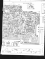
AEP Model
UK Model
rwl
IQUARTZI
tM$TtnE0/Fn||-A]r{
TlJ
N,[fi
SPECIFICATIONS
Frequencyresponse 40Hz- 12.5kH'z+0.2dB
87.5 MHz - 108 MHz
30 Hz- 15kHz 1oà2
dB
300 ohms, balanced
Selectivity
80dB at 300kHz
75 ohms, unbalanced
Captureratio
1.0dB
Intermediatef requency
AM suppression
ratio
1 0 . 7M H z
60dB
Sensitivityat 46 dB quieting (40 kHz deviation)
lmageresponseratio
4 sV (mono)
80dB
43gV (30pV)i (stereo)
lF responseratio
10OdB
1.4FV (S/N= 26 dB, 40 kHz deviation)
Usable sensitivity
Spuriousresponseratio
1 . 8s V , 1 0 . 3d B f ( l H F )
1 0 0d B
'l
FM tuner section
Tuning range
Antenna terminals
Limiting threshold
sV
Signal-to-noiseratio (40 kHz deviation)
80 dB (mono), 75 dB (stereo)
Harmonic distortion (40 kHz deviation)
'100
Hz
0.08% (mono),0.12o/o(stereo)at
0.08% (mono),0.12o/o(stereo)at 1 kHz
0.1% (mono),0.2% (stereo)at 10 kHz
lM clistortion(40 kHz deviation)
Seoaration
0.08% (monol, O.12% (stereo)
45 dB at 100 Hz
50dB (17d8)* at 1 kHz
40 dB at 10 kHz
- Continued on page 2 -
ATTENTION AU COMPOSANT AYANT RAPPORT
À u sÉcunrrÉr
LES COMPOSANTS IDENTIFIES PAR UNE TRAME ÊT
urue ruenoue I
suR LEs DTAGRAMMEs
scxÉMATrouEs,LEs vuEs ÉclerÉes ET LA Ltsrg DEs
prÉcessoNT cRrrrouEs pouR le sÉcuntrÉ oe
FONCTIONNEMENT.
NE
REMPLACER CES COMPO-
sANTs ouE pAR oes prÈces soNy DoNT LEs NUnnÉnossorur ooruruÉsDANs cE MANUELou DANS
les suppt-ÉueNrspuelrÉs pARsoNy.
SAFETY.RELATED COMPONÊNT WARNING!!
C O M P O N E N T SI D E N T I F I E D B Y S H A D I N G A N D M A R K
oN THE scHEMATrc
DTAGRAMS, EXpLoDED
A
V I E W S A N D I N T H E P A R T S L I S T A R E C R I T T C A LT O
SAFE OPERATION. REPLACE THESE COMPONENTS
WITH SONY PARTS WHOSE PART NUMBERS APPEAR
AS SHOWN IN THIS MANUAL OR IN SUPPLEMENTS
PUBLISHED BY SONY.
SONY
MANUA
SERVICE
sT-JX4L
RF intermodulation74dB (lHF),88dB (2.4MHz)
productratio
Sub-carrier
5 5d B
Mutingthreshold Approx.25.2dBl, 10yY
(75kHzdeviation)
Outputlevel/impedance
750mV, 4.7k ohms
tone level
Calibrating
'
50% modulation(37.5kHz deviation),
400Hz
( )* measuredwith the SENSswitchengaged
MW/LWtunersection
Ferrite rod antenna
Externalantennaterminal
46 (42)* dB/m
(at 999 kHz)
54 (50)' dB/m
(at 230 kHz)
40 (30)*rV
(at 999kHz)
50 (40)t sV
(at 230 kHz)
45dB (9kHz)
45 dB (at 999 kHz)
(
75 dB (at 230 kHz)
)r measurèd with the SENS switch engagod
General
System
digitalsynthesizer
PLLquartz-locked
system
PowerrequirementsU K m o d e f : 2 4 O V a c - l o r 2 2 O Y a c - a d j u s t a b l e b y a u t h o r i z e d S o n y p e r s o n n e l ) ,5 0 / 6 0 H z
AEP modef : 22OY ac - lor 24OY ac - adlusta b l e b y a u t h o r i z e d S o n y p e r s o n n e l ) ,5 0 / 6 0 H z
Powerconsumption1 2 W
Approx.430x 55 x 330mm (w/h/d)
Dimensions
(17x 2rltx 13 inches)
includingprojectingpartsand controls
Approx.3.6kg (7 lbs 15 oz)net
Weight
Approx.4.1kg (9 lbs 1 oz)in shipping
carfon
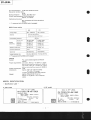
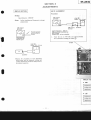
M O D E Ll D E N T I F I C A T I O N
- Specification Label O U K model
A E P model
M O DN
EO
L S. T . J X 4 L
M O DN
EO
L S. T - J X 4 L
TUNER
FMSTEREO/FM.AM
FMSTEREO/FM-AM
TUNER
RANGE'
FREQUINCY
F M 8 7 5 - l 0 8 M H zM W 5 2 2 - 1 6 0 2 k H z
LW l 5 53- 4 4 k H z
: F Ml 0 . 7 M HA
zM450kHz
lF
tzW
50/60H2
AC:22QV
F T Z - P R Ù F N U M MUE1R
85
SERIAN
L O.
4-875-305-OI
M A D EI N J A P A N
F R E Q U E NRCAYN G E :
F M 8 7 . 5l-0 8 M H zM W 5 2 2 - l 6 0 2 k H z
- 3 4 4k H z
L W1 5 5
: F Ml 0 . 7 M HA
zM450kHz
AC:240V50/60H2
tzW
S E R I AN
L O,
IN JAPAN
MADE
4-875-306-0I
2-
ST.JX4L
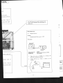
S E R V I C I N GN O T E S
.
THE CERAMIC CAPACITORS
This set uses tube-type ceramic capacitors whose
shape is identical with the carbon resistors. Be careful
not to use resistors instead of capacitors in repairing'
Disc-type ceramic capacitors can be used for
multiplier
temperature
characteilstic
't
st digit
tolerance
replacing those originally used in the set.
Two kinds of drilled holes are provided in some
patterns for mounting the tube-type and disc-type
ceramic capacitors. Use appropriate holes where
2nd digit
Example:
applicable.
Silvering on inside
of tube forming
second electrode.
yellow
wh.ite
;
ceramtc
4
Silvering deposited on outside
of tube forming one electrode.
COLOR CODE (in PFI
Color
lst or 2nd
Digit
brown
I
red
2
l0'
1o'?
orange
J
103
yellow
4
5
gleen
blue
violel
Elay
white
6
7
8
9
0
Multipliet
Tolerance
Y
D
RH
10"
UJ
x30Vo
100
t207o
eold
l0-t
t5%
silver
t0-?
xlÙVo
black
Temperatur€
characteristac
x
SL
CH
V
B
3-
7
l0'15%
SL )
47OpF +5% SL
ST-JX4L
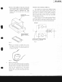
o HandlingPrecautions
for MOS lCs
Generally, the insulation resistanceof the oxide
layer in MOS IC structures is very high, and the oxide
layer is very thin. Becauseof this, it is possible that
3.
the static voltages usually present on clothes and the
human body will be enough to generate a potential
difference across the insulator, high enough to cause
a breakdown of the insulating layer.
The following precautions should be taken while
handling these ICs.
(Particular care should be taken under conditions
of low humidity.)
E q u a l i z e a n y p o t e n t i a l d i f f e r e n c e b e t w e e nt h e
c l o t h e s ,t h e t o o l s i n u s e , t h e w o r k b e n c h ,t h e
s e t b e i n g w o r k e d o n , a n d t h e p a c k a g e dI C b y
o
touching them all in successionwith the hancis
o r a c o n d u c t i v ew i r e o r t o o l .
The following are effective methods for handling ICs that remove the potential difference
a c r o s st h e o x i d e l a y e r .
. Use a paper clip nrodified by soldering in a
wire braid insert.
wire braid
Precautions in Replacing MOS lCs
Store new ICs by inserting them into a urethanepolyester cushion (which is somewhat conductlve), or wrapping it in aluminum foil, so that
all the pins are at the same potential.
(The ICs should be stored in that manner until
mounted on the circuit board.)
soldered
Fig. D
soldered
Make sure that there is
no solder on the inside
clip
Fis. A
Fis. B
2
o
partially conductive
unrethane-polyeste r
cushion
aluminum
foil
Check the solderingiron for possiblepower-line
leakage current. Make sure that there is no
l e a k a g ep a t h b y c o n 4 e c t i n ga n o h m m e t e r t o t h e
partially conductive
u rethane-polyeste r
cushion or aluminum
foil
Fis. E
t i p o f t h e s o l d e r i n gi r o n a n d t h e p l u g a s s h o w n
in Fig. C. If there is a leakage path, use some
o t h e r s o l d e r i n si r o n .
wire braid
VOM
(dl x IO,OOO range)
_
f tg. f
Fis.
4-
Make sure that all the oins are in
contact with the wire braid latt
the pins will then be at the same
potentiat.).
I
I
I
O
Take a short length of fine bare wire and
wind it around the IC so that it shorts all the
pins of the IC, while it is still in the urethanepolyester cushion or aluminum foil. This
ensures that all the pins are at the same
potential.
Precaution while Checking C-MOS lCs
The C-MOS ICs (Complementary MOS) are MOS
ICs that have their output sections made up of
N-channel and P-channel push-pull stagesto increase
their speed of operation. If the output terminal of
these ICs comes into contact with B+ or B- voltage,
then the FET which is ON at that time will either
become shorted or open.
This is valid for all the output sections that are
connected together by the interconnections. Even
the circuits that are physically separated(and not on
fine bare wire
(stripped solid hookup
wtre, etc.J
the same board) can be destroyed simultaneously.
Example:
I
partially conductive
u rethane-polyester
cushion or aluminum
foil
lf this line is grounded, or touches
B+ or B- bus. . . , the output stage
of this lC will be destroyed.
Fis. I
Fis. G
o When it is necessaryto handle the IC with
the fingers, do not touch any pin, and hold
the IC at the ends of its plastic-packagecase
as shown in Fig. H-
Fis. H
Method of Mounting
Insert the IC while holding it with the modified
clip, and solder all the pins with the clip still
shorting the pins. (Similarly, solder all the pins
while the bare shorting wire is still wound
around them.). Remove the clip or the bare
shorting wire only after all the pins have been
soldered.
5-
S E C T I O N1
OUTLINE
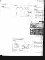
llO (lnput/Output) PORT'S FUNCTION
1-1. CONTROLLER 1C503 (1rPD553C-1371:
Port
Pin No. of lC
Function
PA2
J)
FM Muting ON/OFF Signal.
PA3
36
Memory IC Data Input
PBO-3
37-40
PCo-3
2- 5
PDO-3
8-11
PFO-3
t6-19
PGO-l
22-23
PG2
24
FM/AM Control Output (FM:
PG3
25
MWLW Control Output (MW: I, LW: 0)
PEO
t2
Clock Output for PLL/MEMORY
PEI
t3
$ee next page.
PE2
14
PLL Latch Output
PE3
15
Data Output for PLL MEMORY IC
Level is always H at AM mode.
Seenext page.
I, AM: 0)
IC
PHO-3
26-29
Address Output for Memory IC
Pto-2
30-32
Mode Control Output for Memory IC
6-
5T-JX4L
O S W I T C HA N D D I S P L A Y M A T R I X
LW changeover
OFF Lw, (153-342 kHz)
ON LW, (155-344 kHz)
10.7MHz I 50k Hz
When identitication color
of ceramic filter is blôck or
white, this diode is used.
Switch ing
Matrix
k H z ( = 1 9 . 6 tt t . ,
When identiTication colol
ol ceramic filter is black
this diode is used
CAL TONE CONTROL
SENS CONTROL
'MUTING CONTROL
ENFORCEDCONTROL
7-
ST.JX4L
=
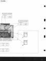
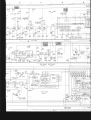
1 - 2 . B L O C KD I A G R A M
v
IJ . I
à l,'l
F]
g
g
Ëtr
aÈ
Èt
t:i
frf,
* ==r
.l
I
t_
t*
I
I
LEIEr E FI
L-El---l
oF<
E
L!
8-
1.3. TUNING WITH THE STATION PRESET
BUTTONS
With this tuner, owing to an electronic tuning
system using a PLL (Phase Locked Loop) synthesizer
and a memory circuit, the reception of a station is
much simplified. Once you commit the frequencies to
memory, pushing a button is all you need do to select
a desired station. There is no need to search for the
station with the TUNING button each time you wish
TO MEMORIZE THE STATION FREOUENCIES
Preparation: A total of eight station preset buttons can be preset for either FM, MW or LW in any
desired sequence. Arrange the order of stations for
each station preset button and note the band and the
frequency of each in advance.
to tune in a station.
Follow the numbered seguence.
@
Note that the setting of
the f^lôi,Î,Zt
and SENS
switches for reception
of this station is memorized.
llluminates for a few seconds,
Repeat these steps for each station preset button.
Replace the station labels to conform to the
selectedprememorized stations.
WOit" the MEMORy indicator is iiluminated,
press the desired station preset button.
The indicator will go out, and the band,
frequency and setting of the rlaLj!,È^,z,
and
SENS switches will be memorized.
TO CHECK THE PRESET FREOUENCY
After the memory procedure is completed, confirm the prememorized frequency. Pressthe TUNING
button and change the frequency display indication.
Press the station preset button to be checked. The
frequency which had been pre-memorized should
Notes:
o The MEMORY indicator will go off automatically
after a few seconds. When the indicator is out, the
memory circuit does not operate to memorize the
station.
a The previous memory will be erased when a new
frequency is committed to the memory of the same
button. An erasure cannot be made without a new
input.
then be indicated in the band/frequency-display window.
TO RECEIVE A PRE{VIEMORIZED STATION
Turn the POWER switch on and simply press the
desiredstation preset button.
To memorize a weak station
Memory of the last received station
To memorize MW and LW stations whose signals
are weak or whose strength is variable, tune with the
SENS switch engaged. To memorize weak FM stations, tune with the SENS switch engaged and the
This tuner includes a memory circuit to remember the station which had been received for
more than one second just before the power was
turned off. This station will be automaticallv
tuned in when the power is turned on again.
This memory system enables you to make a
timer-activated recording from the tuner.
ff|f,'r$l switch disengaged. This will ensure the
onetouch memory reception of those stations.
9-
ST.JX4L
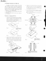
S E C T I O N2
DISASSEM
BL Y
y r o c e d u r ei n t h e n u m e r i c a lo r d e r g i v e n .
Note: Follow the disassemblp
Top Coverand Front PanelRemoval
O e vT T 3 x 6
o O, O: top cover
o O-@:
frontpanel
p
BVTT 3 x 6
,P
EVTT3 x 6
,P
y'front panel
l-..o.XU'y'j
@ avrrsxo
@ avrrsxo
Bottom Plate Removal
(l):
Loosen the eight screws
(BVTT 3 x 6).
(2): Remove in the
direction of
arrow.
'og
o
1s
not loose these screws.
10 -
I
ST.JX4L
sEcTloN3
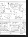
ADJUSTMENTS
AM IF ALIGNMENT
MWLW SECTION
Procedure:
Setting:
AM rt signal
Band Selector: MW/LW
Setup:
generator
before tracking and frequency coverage
adjustments
AM antenna
terminal
AM rf signal
generator
Put the lead-wire
antenna close to
the set.
Carrier frequency:
999 kHz
30% amplitttde modulation by
4OO Hz signal
Output level: as low as possible
.
30% amplitude
modulation by
400 Hz signal
OUTPUT
Tune the set to 999 kHz and adjust IFT3OI
for a maximum readingon VOM @.
voM @
m
(range: 0.5-5Vac)
OUTPUT
. Repeat the procedures in each adjustment
severaltimes, and the frequency coverageand
tracking adjustmentsshould be finally done by
tlle trimmer capacitors.
1-
I
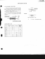
MWLW FR
I
o tvtw
|
| FrequencVI
I
l-
I l-t.lt"s" ". r
I l-Adj'"."*
tor_w
1
Il T - I F"qr"*yI
|
| Voltage at T
lr|
| edjustment
t-
ST-JX4L
VOM (dc range)
VOM {dc range)
ry
ry
t,602kHz
522kHz
22V
1 . 5V
cr304
T302
344kHz
155kHz
1 8 . 5V
2.3V
CT3O2
T301
-
t2 -
sT-JX4[
FM SECTION
Setting:
STEREO/MUTTNG
swtch:
Band Selector: FM
l.
2.
Tune the set in the st
Adjust the black core
for 0 V readingon VOIri.
Note: When replacing the
ceramic
form this alignment.
Repeat the secondary_sidb
ments several times.
I
tFTtol
(primary side: black
core)
FM Discriminator Alignment
z
Setting:
Procedure:
STEREO/MUTING switch:
OFF
Adjust the white core (
IFT102 for minimum distortion.
FM rf signal
generator
Note: When replacing the ceramic
form this alignment.
Repeat the secondary_side
mentsseveraltimes.
FM antenna
terminal
Carrier frequency:
uutput tevel:
Modulation:
-
13 -
OUTqU
OUTPUT
gg MHz
I mV (60 dB)
4O0 Hz,40 k'Hz deviation (lOO%t
ation-signal.
-side) of IFTl0l
(CF101- 104), PerprimarY-sideadjust-
the
The FM front'end is carefully adiusted at
for
factory and is supptied as one whole blæk
replacement.
'F
cs
:d.
VCO Adjustment
A)
RegularMethod
rse
Setting:
STEREO/MUTINGswitch: OFF
)M
Procedure:
FM rf signal
generator
'r#i,':i'"
white core)
98 MHz
4oo H2,40 kHz deviation ('oo%)
I mV (6OdB)
-'
Carrier freguencY:
i,,";;;;"';tt;;-Ouput tevel:
Tune the set to 98 MHz by pressing the
MANUAL TUNING switches'
the
Adjust RV20l for lgkHz 1 l00Hz on
counter.
i:ii::::,iii;!tii
:iiii:
TP5
frequencycounter
(CF101- 104), Per-
mark iii
with l"
R206
e€+
primary-side adjust-
;::iii:,:,ii,li::ii
,,,:.:,::,:,:l
: :::,:j,
:t:,1::l:.::,:::,:
!t une ,,
Ne les ,,
"rméro i:
-
14 -
FM SECTION
Setting:
Band Selector: FM
FM StereoSeparationAdjustment
Setting:
STEREO/MUTINGswitch: ON
Procedures:
FM rf stereo
signal
generator
FM antenna
terminal
OUTPUT
Carrier freguency:
98 MHz
Output level:
1mV (60dBl
Modulation:
Audio (400 Hz):
16.25kHz deviation (40%)
Pilot (19 kHz):
7.i kHz deviation (tg%)
Sub-channel:
16.25 kHz deviation (40%)
FM stereo
signal generator
output channel
VTVM
connection
L{H
VTVM
reading(dBl
L{H
@
a)
R{H
Adjust
RV202 for
minimum
reading.
L{H
R{H
R{H
@
@
Adjust
L{H
R{H
RV202 for
minimum
reading.
L-CH Stereo separation:
R-CH Stereo separation:
The separations of
equal.
Setting:
CAL TONE switch: ON
Procedure:
VTVM
lml
@-@
@-@
both
CAL TONE Level Adjustment
channels should be
E+-J
OUTPUT
Adjust RV203 for 0.39 V (-6 dB) reading on
VTVM.
*
15
-JX4L
r'|:rill
,.:ll:i:
''.11.1
.l::ll'llii
..,uutl:
'rrl:li:
:r];1
rlii*{i
FM Muting LevelAdiustment
%
Setting:
STEREO/MUTINGswitch: ON
Procedure:
FM rf signal
generittor
VTVM
FM antenna OUTPUT
terminal
Carrier frequencY:
'
Ii;e;i";it;'
Output levet:
98 MHz
4o0 Hz,4o kHz deviation (t0o%)
10 PV (20 dB)
Tune the set to 98 MHz by
MANUAL TUNING switches.
pressing the
Adjust RV 101 for a 0 V reading on the VTVM'
-
16 -
S E C T I O N4
DIAGRAMS
4-1. MOUNTING DIAGRAM
- Conductor Side SemiconductorLead Layouts
25D880
2SC181s
2SC1364
2SC1362
2SC1890A
2SA1015
rh
W
ililil
n
ilil|
,/l\
'cB
hil'
l\
2SK30A
2SC710
r)
mil
ilflll
/f(
eci
KV1226-D
lelter srde
m
N,
ÊYl
cx76tA
cx778
LA1235
LA1245
L43390
rrPD552C-O65
pPD4Ol1C
,fi,
slrl or
1S1555
1082
EOA0l-OsR
EOA0l-06R
HZ6B2L
HZ16-2L
HZ3G3L
cat hode
(Top vrew)
L-sNG1O
L-5PR5
L
/
ti
â
tl
VP
ll- ànooe
CLOCK
GENERÂTOR
BIÏS DATAREGISTER
n
STATION
:MORYÂRmr
( t4 w0RDS
x r 6E r T s )
ffi
to.o-Jl sno'r
l[-llt.
/
anode
cathode
! PD553C-073
FM Ceramic Filter Adjustment
Identification color of FM
ceramic filters (CFl 0l-l 04)
O: to be connected, X: to be removed
Notes:
.
.
.
C o l o r c o d e o f s l e e v i n go v e r t h e e n d o f t h e j a c k e t .
i-F
: i n d i c a t e ss i d e i d e n t i f i e d w i t h p a r t n u m b e r .
: B+pattern
o -f-:
. rrr>:
. -.rrr.r}:
s i g n a lp a t h
L - C H s i g n a lp a t h
R _ C H s i g n a lp a t h
-
t7 -
ITUNERBOARDI
$tW=ry.;m
.-
c4r3o.r/5ov
I
die{
r
'sË:i
L
llffidi.'tËm,
f'Ë$r#i
'S\t'æar
\i
r F . o u r)
-_<-/
|
...F.OU.T
r-Q
*5*
'4
ï'iis'"
l;tltËlffi#J
{
;î,
,9i-.,,
Ë1*-,$E#I *Ë',Y.
,,!r,,',;;.t'''
i{*.
#;*''1
;tT;r
=iJ
Ti+ifi+:r
Eli
"+i
ffi##y
ô vcc
,
c305 l0os/
i'
;%,
i*o'
io0?2
Tal
cFro4qft,tol
oto>,
cno:g*,F
4 2 v5
4.lv
Rl15: u*
.î
jËur'î,u,/
-?!1
3 lë 1 ,
tiâ;.*
'ftJ*$*,-t=/
ffiÆ
o+
qç'"
-- '',fi'u
.3y
I
o99
ffiï
6t
'
glc#
8aJvu.
., -t-i
x4ql
'1_
:+
'.F
xTsT
I
3À3ô 'eé ',r
À
(PRESET
BOARDI
s803
E]
s806
L9J
s807
I
r0l toz
404403
406
r03 104502
501
rô5
302-2
30r- 2
501
1ô
303
106
503
308
tc502
1c503
302-l
3 0 1 -I
302
30r
t cl 0 l
(OUTPUT
BOARD)
n#a'#ËnJ-ffi.Ë
;t HHcfËil$:F}iRâ
#trffiffil Llr;u"
ffi,,*-wffiffffi
.*ï,,
t:";'{
ff;-riry:
t*
ffLffrqÆ#'fÏ',ruï
rH
Ime;nz.
*i':,çLL
l,,
qfiffiffid#{,l
i':ffi
=*'.ffiJï'',
ffiæ1F#ffi
Iu11ffdË+:iiu;æ
ËiïË"
p ,,-fi{;ff,f
d]il
giih
Ë-T
i-r.
o.| I
?
, ;rP.5...;
,/ ,
R206:fl2L
R ô E 1; 9 ;
"
r& .,.1.1,'#ff*
#fu**
.t^.r
:-
TÊ#*lJe,:-{
f]IÀlI Eî;f.".ffi'#geef,,.,
^5' lo,-l
hhru4ffi
f*lïfii''jjfl
Iw,f
iffi J;
ffil"HïJllffi:Y,ffi=
1lI I sTul
; ; a 1 â ââ
lltffii
I
I
lztYt!l2J:
It t It llËlFrrr;l:
llll
-**
R55B22t
I
sTclslsT
_+g*Ë
.!-'v.
Ë
ÈiJÈJÈJÈI
l È i $ li s l i il l l
J
I
*-fl--
^y
D6t3
|
{ oouÔ4"''..'''.."
so+
" ï'"''','','''*
lls J
rl1r o
"r
l o n 'i"
I
1l
T
I
I
a
1
cl
rlhllllrr'J
rJr
rlll
ôl
I
ll
TliTlTTli
tltlttill
6ô
ô
ô6ô
(CHANGE
SWBOARDI
504 505
tc20l
tou
'0 r,,u,,u?Pt'3îrurl9
206
205 203204
20t 202 207
tc505
zoa
610 -^
609
608
gg5
fff
.ro.
C#
tc504
6117
ôÀ(\
!P040r3c
B+
!PD40l3c
E1
Note on Schematic Diagram
pF: ppF
are in pF unless otherwise noted'
.- Àtt
""p""ltors
except for electrolytics
not
indicated
are
less
or
50WV
and tantalums.
r/" W unless otherwise noted'
. All resistors are in ohms,
k
a
:
1
0
0
O
M
o
ko : IOOOO,
nonflammableresistor'
. @['
.
A : internalcomponent'
r [--_l : adjustmentf or rePair'
B+ bus.
. é..
B- bus.
. ---:
g r o u n d u n l e s so t h e r w l s e
. Voltages are dc with respect to
noteo.
with a VOM
r R e a d i n g sa r e t a k e n u n d e r d e t u n e d c o n d i t i o n s
(20ka/v).
no mark: FM
<>:AM
ON position
<< >>: FM ...STEREO/MUTING:
s
i
g
n
a
l
s
t
e
r
e
o
i
n
F
M
:
T
u
n
e
d
II
tt
due to normal producVoltage variations may be noted
o
(UP)
M A N U A LT U N I N G
s701
M A N U A L T U N I N G( D O W N )
s702
AUTO TUNTNG(DOWN)
s703
A U T O T U N I N G( U P )
s704
STEREO/MUTING
s705
CAL TONE
s706
MEMORY
s707
FM/MW/LW
s708
_8)
s 7 0 9 - 7 1 6 P R E S E T( 1
s801
I
r$
: signal Path
::i:li::]l::::i1i::::il:i].i::iii:i:.:i::::!ii|
andt11!! il
iiir,Note:The componen; 'J"itirita bv shadins
with :lli
only
ileplace
,{'-ai"-"titi""t-ioi satety'
ir
spocified.
ii
frti;;b;t
iiiiii..iiiiÏ::lii::lïi:liiii::i.,i.::iii:::|ii:.lii::::iiii:iiii:::iiiÏii:iiiii:iiii::iï:ii.,iiiiÏiili,iiiil::i;...,I
Les compasdrrl' ruE"r!"v'
Ju, r" sc"utitc. Ne les i.,:
,,,
marque I sont
"titigl-"t-lr-^ ^^,râhr rc numéro
iïli,,i#;i:'pi;';i;;iè*
sPécifié.
-20-
ri
pôruntrenuméro
A
Ttc
(TUNER
BOABPI
FEIOI FM FRONTEND
AI
FM RF AMP
Q2 FM MIX
fl rryld
r
L
T
l=oonl
L
03 BUFFER
@
04 osc
-1
E
Rl40
220r
R19
I
I
'ï
I
I
I
I
I
l_
*n[û'r.rr,t,
T
ROOAiII
ll'
Lf,
Itu
tl
tl
tl
tl
tl
ll
tl
tl
tl
tl
tl
tl
tl
ll
ll
tl
u
30.6V rc402 )_
o.o22T
R409
2.2k
R42C
2.2k
lc40t cx778
PLL
0405 i
cLi
2 . q\
c404
560
tcl0t
LAl235
IF ÂMP
0 l0l -
106 ZSCZIO
F MI F
,'d'8ifi.W
"&r7+
tù,
Rr06
330
Ril|
330
*l'i*
ce3
0.022.
- 31,'
5.4V
0306,307
25Cr8t5
ÂMB+
D S T A I T]
CN 5V
tOFF 0.6VJ
0304 2SCr8r5 Q305 2SCl815
Atv F|LTÊR
D50trsl555
0502 2scl8l5
srvrlot
050 I
050r2scr815
CLOCKCONTROT
SWITCH
0306
!.i,
12.2\jj
lc20l
Q207 2SCt890
CAL TONE
R232
561
e2l
0.0068
zSCl8l5
oso3
i
,r*
,r,olu-lr,
?1
11
,r-,0 ,-r,, G,.--l 1l-.lr
1ryryryryEFryry1
il+1
11
1?
1?
ee
ee I
FDsOI(FLUORESCENT
DI
1r'reNonv-l
i--l i-
i Ffl'qiii
t------ -l -l '-
t--*--11
L=
PP P GP P PP G P
dAM
o M H z r a -,
I
MEMl(HzuV7MWFM b
I
_l
0203 zSCt8t5
Q2042SAr0r5
0 2 0 r , 2 0 22 S C r 8 r 5
s wI l c H
sf,'lTcH
TOUTPIJT
BOA
I r srrrrl
, cN 4.8!
I i O FF j . 8 v l
*{ô
tv
R227rk
tf-l
Iro""tI
l--@l
OV
R2l9 rr
îEl
_l__
0607 2SCr890
POWERIVUTE
D612tSr555
)t8t5
UFFER
{t"ii'J T{f
R238
Q602 2SCl8l5
ERROR
DETECT
rcso+,sos
I
zl0l3C
!PD
LATCH
-
TUBE)
J
L
hiri)'l
- -i i| |i- i i---- lcÂfror're
]
iii lltZti!- rx' jjorsranr;
iittii-4!J-rr.-iirLTtrGi
PGGPGPPPGPPG
cr
e 4 3 br 2 o,o' caLz o6 MUTI
e,
6ltl
F F
HZ30 0605
TNVERTER
I
t
|
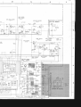
S E C T I O N5
E X P L O D E DV I E W S & PARTS LIST
B
c
"ffi
5T.JX4L
ST.JX4L
ST-JX4L
A C C E S S O8RPYA C K I NIG
,IATERIAL
G E N E R ASLE C T I O N
No.
1
2
3
4
5
6
7
B
9
10
Part No.
D e s c rpi t i o n
No.
Part No.
D e s c r pi t j o n
3 - 7 0 1 - 0 3 0 - 0 0L A B E L S
, E R I A LN U M B E R
3 - 7 0 1 - 6 9 0 - 0 0L A B T L( I 4 A D IEN J A P A N )
3 - 7 0 1 - 7 4 8 - 0 0CLA14P
3 - 7 0 1 - 9 9 3 - 0 0S P A C E R
Ï I,R I 4 I N A L
3 - 7 0 3 - 0 4 3 -I2 L A B T L C
, AUTION
I 4,A I N
51
52
53
54
55
1 - 5 0 1 - 1 6 1 - O OA N T E N N A , F E E D T R
1 - 5 5 1 - 7 3 4 - 1 1C O R DC, O N N E C T(TR0KN- 7 4 A )
3 - 7 0 1 - 6 3 0 - O OB A G ,P O L Y E T H Y L E N E
3 . 7 8 3 - 5 3 1 - 1 1M A N U A ILN, S T R U C T I O N
( Dr ^Ui T
3 - 7 9 5 - 1 8 6 - 1 1( A t p ) . . . M A N U A L , t N S T R U C T T 0&N S
EC
DH
ISH)
3-703-244-00 B U S H I N G
C ,O R D
3 - 7 0 3 - 3 2 8 - 0 0 ( A E P ) . . . . 1 A 8 [ 1A, P P R O V4A C
L OUNTRIES
3 - 7 0 6 - 1 6 5 - 0 0SCREI^J
3-831-441-XX
CUSIlION
SP
, TAKER
4 - B t r - 3 2 2 - 0 1 C A P ,P O W EKRN O B
56
51
58
59
60
61
4 - 8 7 5 - 0 4 0 - 0 0 S H E E Tp. R O T E C T I 0 N
4-815-042-00 CUSHI0N,
LOl,lER
4 - 8 7 5 - 0 4 3 . O OC U S H I O N
U,P P E R
4-875-313-OO
L A B E L( E P ) , I N D I C A T O R
4 - 8 7 5 - 3 5 5 - O OI N D I V I D U ACLA R T O N
9-910-999-47 LABEL.SEAL
4 - 8 7 1- 3 2 3 - 0 0 B A S E ,P O l i E K
I1
RN O B
1 2 . ; 4 - 8 7 5 - 0 0 4 - 3 1P L A T EJ, A C K
(L), SIDE
1 3 . ; 4 - 8 7 5 - 0 1 7 - 0 0P L A T E
1 4 4 - 8 7 5 - 3 0 5 - 0 0 ( A E P ) . . . . L A B E rL,,r 0 D ENLU T 4 B E R
UK)
1 5 4 - 8 7 5 - 3 0 6 - 0 0L A B E L r, 4 0 D ENLU M B T( R
(3), PROGRAM
16 4-875-319-2r K N O B
(6), PROGRAM
1 1 4 - 8 7 5 - 3 1 9 - 5 1K N O B
1B 4-875-319-tr K N 0 B( B ) , P R 0 G R A [ 4
l 9 ô ; 4 - 8 7 5 - 3 2 5 - 0 0B R A C K EC
T ,H A S S I S
I ,)], D I G I T A L
(C
2 0 4 - B 7 s - 3 2 6 - 0 1I , 1 I N D O
2 1 . ; 4 - 8 7 5 - 3 2 7 - 0 7H E A T
SINK
2 2 t ; 4 - 8 7 5 - 3 2 9 - 0 0 B A S E ,T R A N S F O R [ 1 E R
2 3 4 - 8 7 5 - 3 3 0 - 0 0l r 0 L D E(R8 1 ) , S C A L ED, I A L
24 .;4-87 5-332-00 H O U S IS, I G N A L
2 5 . ; 4 - 8 7 5 - 3 3 3 - 0 0R E T A I N T ÏRU, B E ,I N D I C A T I O N
2 6 4 - 8 7 5 - 3 3 5 - 0 0L A B E L( D ) , I N D I C A T O R
27 .;4-875-336-02 CHASSIS
C,E N T E R
2 8 . ; 4 - 8 7 5 - 3 3 7 - 0 0 P L A T EB
, OTTOM
2 9 . ; 4 - 8 7 5 - 3 4 0 - 0 0C H A S S I S
S ,U B
3 0 4 - 8 7 5 - 3 4 1 - 0 0CAST
31
32
33
34
35
4 - 8 7 5 - 3 4 3 - 0 0L A B T L ,L I / S T L E C Ï I O N
4 - 8 7 5 - 3 5 4 - 0 0I N S U L A T O R
7-685-1
3 2 - 11 S C R E+WP 2 . 6 X 5 T Y P T N
2 ON-SLIT
7 - 6 8 5 - 6 4 6 -11 S C R E+t ,Bl V T P 3 X B T Y P E 2N - S
+BVTT 3X6 (S)
7 - 6 8 5 - 8 7 1 - 0 1SCREl,r
36
37
3B
39
40
7 - 6 8 5 - 8 7 1 - 0 9S C R E+WB V T T 3 X 6 ( S)
7 - 6 8 5 - 8 8 0 - 0 1S C R E+WB V T T 4 X 6 ( S)
9-911-845-XX
CUSHION
9 - 9 11 - 8 4 6 - X XC U SIH
ON
( TRR A N S F O R M E R )
9 - 9 11 - 8 6 3 - X X I N S U L A T O
4 1 9 - 9 11 - 8 6 3 - X X C O V E RE, D G E
42 A-4322-339-A P A N EALS S YF,B O N T
43 r ; A - 4 35 1- 2 5 0 - A M O U N T P
EC
D B ,T U N T R
-O64-A KNOB
44
A-4447
ASSY,POl^jER
0
4 5 x - 37 01 6 9 - 0 F O O T
A S S Y ,1 4 . F
46 x - 4 8 75- 30 1- 0 K N O B
A S S Y ,P R T S E T
N O T I:
' I t e m s v { i t h n o p a r t n u m b e ra n d n o d e s c r i p t j o n a r e n o t s t o c k e d b e c a u s et h e y
are seldomrequired for routine service.
' I t e m s m a r k e d" ô " a r e n o t s t o c k e d s i n c e
they are seldomrequired for routjne
s e r v i c e . S o m ed e l a y s h o u l d b e a n t i c i pated whenordering these items.
' D u e t o s t a n d a r d i z a t j o n ,p a r t s w i t h p a r t
n u m b e r s ( a - A A A - a A A - x xo r A - A A ^ A - a A A - X )
maybe different from those used jn the
set.
C A P AICT O R :S
' All capacitors are in
u F . C o m n o nc a pacitors are omjtted. Refer to the
following lists for thejr part numbers.
M F u: F , P F : U U F .
R T SI S T O R S
' All resistors are in ohms. Common
1 / 4 W , 1 / 8 Wa n d 1 / l 6 W c a r b o n r e s i s t o r s
a
' Ir e o m i t t e d . R e f e r t o t h e f o l l o w i n g
ists for their part numbers.
' F : nonflammable
COILS
'MMH:mH,UH:uH
-27-
T h e c o m p o n e n t si d e n t i f i e d
by shading and markf\are
c r i t i c a l f o r s a f e t' vp .aor t
Replace only with
n u m b e rs p e c i f i e d .
L e s c o m p o s a n t si d e n t j f i é . s P a r
une trame et une marque/Àsont
crit'ioues oour la séciïité.
N e I e s r e m p la c e r q u e p a r
une pièce portant le numéro
s p é ci f i é .
-!l
ST-JX4L
E L E C TIRC A L P A R T S
Ref.No.
Part No.
ELTCTRICALPARTS
D e s c ri p t . i o n
Ref.No.
5 0 6 r ; 1 - 5 3 5 _ 1 2 0 _ oT
oERMINAT
5 0 7 r ; 1 - 5 3 5 - 1 2 1 _ o oT E R M I N A L
5 0 8 r ; 1 - 5 3 5 _ 1 4 0 _ 0B
0 ASE
POST
MI I C H )3 p
1 9 M t(41 O M p
s09
t - 5 3 6 _ 6 6 3 _ 0 0r r R r 4 r N AeLO n n oi À N i l N r i À i
"^'
510 A.t-str-bs4-o0tuit....cono,"pôiËR'
Pôrt No.
Dpscrinfiôn
D30B
D309
D401
D402
D403
8 - 7 1 9 - 8 1 5 _ 5 5D I O D E
1S1555
B - 7 1 9 - 8 1 5 _ 5D
5 IODE
1S1555
8 - 7 1 9 - 9 1 2 _ 0 0DI ODEI.4V-1
2N
B-719_912_00
DIODE
MV-12N
8 - 7 1 9 - 8 1 5 _ 5 5D I 0 D r1 S 1 5 5 5
D404
D405
D501
0502
0503
8 - 7 19 - 8 15 _ 5 5 D I O D Ê
1S1555
B - 7 1 9 - 851_ 5 s D I O D E
1S1555
B - 7 1 9 - 8 1 5 _ 5D
5 IODE
1S1555
8 - 7 1 9 _ 8 1 5 _ 5D
5IODE
1S1555
B - 7 1 9 - 851_ 5 5 D I O D E
1S1555
,iiâ,,,,_.i
!!â.ïii:!ô
iijjil;
iiil5qti3o?],0,_,uou,
5i3 &1-553-3rB-00
pusn
inc-poue;i
i:fif
YIll;
?
1 4 r - 5 5 3 - 7 4 2 s- 0r g0 l' r gnHu, a s ri ri li - i i b i l _ r o r o l
515
r ; 1 - 5 6 0 - 5 9 5 - 0T0E R [ , t r N
l wArLr Ha n s r i - - - -
5 1 6 r ; 1 - 5 6 1 - 4 7 1 - 0 0S O C K E C
T ,O N N E C T
OR
6p
517
5 1 8 r ; 1 - 6 0 5 - 0 3 5 - 0 0 P CB O A R DR, U B B TSRH E T T
Kty Sr^1
519
1 - 6 0 5 - 4 7 2 - 0 0P C B O A R DT,U N E R
520
1 - 6 0 5 - 4 7 3 - O OP C B O A R DP, R E S T T
521
1 - 6 0 5 - 4 7 4 - O O P C B O A R D ,L E D
522
523
524
pc gonno,pot^ltR
1-605-475_00
s|^]
1 - 6 0 5 _ 4 7 7 _ 0p0c e o R n oC
, HANS
GlE^ t
l - 6 0 5 _ 4 7 8 _ 0p0c s o n a o ,o u r p u i
ç?q?
c304
c326
ç111
c414
1 - 1 6_13 8 0 _ 0 0c r R A M r c
0 . 0 05
1M F n %
1 - 1 0 8 - 3 5 2 _ 0M0y L A R
o .ô o r à r , r r n %
1 - 1 6 1 _ 3 1 8 _ 0c 0
ERAt4tc :sopFrc%
0 - 5 9 3 _ 5 6 5 _c A P ,E L E C T0 . 6 B M F
0 - 5 9 3 - 5 6 5 _ c A P ,E L E C TO . o e M r
D504
D505
D506
D507
D508
8 - 7 1 9 - 8 1 5 - 5 5D r 0 D E1 S 1 5 5 5
8 - 7 i 9 - 8 15 - 5 5 D I O D t1 S 1 5 5 5
B - 7 1 9 - 8 1 5 - 5 5D I O D E
1S1555
B - 7 1 9 - 8 1 5 - 5 5D r 0 D E1 S 1 5 5 5
B - 7 1 9 - 8 1 5 - 5 5D r 0 D E1 S 1 5 5 5
D509
D510
D51
I
D512
D513
8-719-85
1 _ 5 5 D r O D E1 S 1 5 5 5
8-719-815_55
DrODE
1S1555
8 - 7 1 9 - 851_ 5 5 D I O D E
1S1555
B - 7 1 9 - 8 1 5 _ 5D
5 IODE
1S1555
B - 7 1 9 - 851- 5 5 D r O D E
1s1555
D514
0515
D516
D51
7
D5l8
8 - 7 1 9 - 8 1 5 _ 5 5D I O D E
1S1555
8-719-815_55
DIODE
1S1555
8 - 7 1 9 - 8 1 5 _ 5 5D I O D E
1S1555
8 - 7 1 9 - 851- 5 5 D I O D E
1S1555
8 - 7 1 9 - 851_ 5 5 D I O D E
1S1555
50\/
50tl
50v
D 5 1 9 B - 7 1 9 - 851_ 5 5 D I O D E
1S1555
D 5 2 0 8 - 7 1 9 - 8 1 5 _ 5 5D I O D E
1S1555
D 5 2 1 B - 7 1 9 - 851_ 5 5 D I O D E
1S1555
D 5 2 2 B - 7 1 9 - 851_ 5 5 D I O D E
1S1555
l:rrl9?]'r's{$0:::rr:]cE}a}{t'c,::r,::::r.,r']rl#]Ëàsmlrrr!:l:{l!:!:rirl:ï:l?s0vrl
,rr:ç,e0!|&t
D 5 ? 6 8 - 7 1 9 _ 8 1 5 _ 5D
5 I O D t1 S 1 5 5 5
c F 1 0 1 1 - 5 2 7 _ 8 3 6 _ 0F0] L T E R , C E R A M I C
cFt02 1-527-836_00
F I L T E R ,C E R A M I C
c F l 0 3 1 - 5 2 7 _ 8 3 6 _ 0F0I L T E R , C E R A M I C
cF104 1-527-836_00
FILTER, CERAI4IC
c F 3 0 i I - 5 2 1 - 8 ? 6 _ 0 0F I L T T R , C E R A I 4 I C
cF302 1-527-817_OOF I L Ï E R , C E R A T 1 I C
cT301
cT302
cT303
cT304
1 - 1 4 1 _ 1 7 1 _ 0C0A P , T R ] I 4 M E R
1 - l 4 i _ 1 7 1 _ 0 0C A P , T R I M M E R
1-141-180_0C
0 AP, TRIMI4ER
i - 1 4 1 - 17 1 _ 0 0 C A P , T R ] I 4 M I R
D207
D20?
D203
D301
D302
8 - 7 1 9 _ 851_ 5 5 D r O D t1 s 1 5 5 5
8-719-815_55
DIODE
1S1555
8 - 7 19 - 8 15 _ 5 5 D I O D E
1S1555
B-719-912_27D I O D T
KV1226
8-719-912_27 D I O D E
KV1226
D303
D304
D305
D306
D307
B - 7 12 - 6 0 0 _ 0 0 D ] O D E
1T26
B - 7 12 _ 6 0 0 _ 0 0D I O D t1 T 2 6
B - 7 1 9 - B5l_ 5 5 D I O D ti s 1 5 5 5
8 - 7 i 9 - 8 15 _ 5 5 D I O D E
1SI555
8-719-815_55
DIODE
1S1555
NOTE:
' Items.wjth
n o p a r t n u m b e ra n d n o d e s _
c r r p t t o n a r e n o t s t o c k e d b e c a u s et h e y
a r e s e l d o mr e q u i r e d f o r r o u t i n e s e r u l c e .
' Items
m a r k e d" ô , ' a r e n o t s t o c k e d s i n c e
they are seldomrequired for routine
s e r v i c e . S o m ed e l a y s h o u l d b e a n t i c i _
p a t e d w h e no r d e r i n g t h e s e r r e m s .
' Due,
to standardization, parts w.ith part
n u m b e r s( A - A A A - A A A - XoXr A - A A ^ A _ A A A _ X )
maybe different from those used in the
set.
llMtô]l$lisiii9{*d&ôâ,li
ot.oD[,.
ffi64,,
-
:r'8€8*riu.8i{i${*g#*
BiSBF
iÉ!!''
i]::r,:,ir:,,r.,:rl::r']r::r,l
i..i.'r:r.i,r,'.:,.,i
.x8$$rw8!rl,l&iffi86;:,BiS#
i#i': .",,;,.,r,,:r,,,i:,rr,
D611
D612
D613
D701
D702
8 - 7 1 9 - 9 1 3 _ 0 2D ] O D EH Z 3 O - 2 1
B - 7 1 9 - 851_ 5 5 D I O D t1 S 1 5 5 5
8 - 7 1 9 - 9 3 6 _ 0 6D r 0 D Er Q A 0 1 - 0 6 R
B - 7 1 9 _ 9 5 1 _ 0D0 I O D T
GL-5NG1O
B - 7 1 9 - 9 0 0 _ 5 6D I O D E
GL-5PR5
F E 1 0 1 1 - 4 6 3 - 3 6 9 _ 0 0F R O NE
TN D
F 1 5 0 1 t 5 I 9 - 2 2 9 _ 0 0 INDICATORTUBE, FLUORTSCENT
CAPAC
I TORS
:
' All.capacitors
a r e i n u F . C o m m ocna _
pacrtors are omitted. Refer
to the
following I jsts for their part numbers.
M F : p F ,P F : u u F .
R I S] S T O R S
' All resistors
are in ohms. Common
1 / 4 W , 1 / 8 Wa n d l / l 6 W c a r b o n r e s j s t o r s
are-omitted.
efer to the fo)lowing
l l s t s t o r t h e .i R
r part numbers
C OL
IS
. MMH
: ufl
-28-
T h e c o m p o n e n t sj d e n t i f j e d
by shading and markAare
critical for safety.o
R e p l a c eo n l y w i t h p a r t
n u m b e rs p e c i f i e d .
L e s c o m p o s a n t si d e n t i f i é s p a r
une trame et une marquef\sont
critiques pour'la séffiité.
Ne I
r e m p la c e r q u e p a r
u n e p"i:e c e p o r t a n t l e n u m é r o
j
spéc fi é.
ST-JX4L
E L E C T R I CP
AA
LR T S
E L E C T R l C APLA R T S
Ref.No.
Part No.
IC101
IC201
I C301
IC401
IC501
-.-:J'
Ref.No. Part No.
DescriPtion
8 - 7 5 9 - 8 1 2 - 3 5I C 1 A 1 2 3 5
8 - 7 5 9 - 8 3 3 - 9 0I C L A 3 3 9 O
8 - 75 9 - 8 12 - 45 I C 1 A 1 2 4 5
-78 I C C X - 7 7 8
B-759-601
8 - 7 5 9 - 1 4 0 - 1 1I C U P D 4 O 1 1 C
I C s 0 2 8 - 7 5 7 - 6 1 1 - 0 0I C C X - 7 6 1 4
qÛ3^4-7â9:l' 31- 37 I C U P D 5 5 3 C _ 1 3 7
I C 5 0 4 8 - 75 9 - 14 0 - 13 I C U P D 4 0 1 3 C
I C 5 0 5 B - 7 5 9 - 1 4 0 - 1 3I C U P D 4 O 1 3 C
RC
, RIMINATOR
I F T 1 0 11 - 4 0 4 - 3 3 9 - 0 0T R A N S F O R MDEI S
(FM)
I F T 1 0 21 - 4 0 4 - 3 3 8 - 0 0r n n r ' r S r O n U rDnI,S C R I t 4 I N A T O R
TR,
I F T 3 0 11 - 4 0 4 - 3 2 6 - 0 0T R A N S F O R MI F
1301
L3O2
1303
1401
22
INDUCTO
RO U H
MICRO
1-407-173-XX
39
INDUCTO
RO U H
MICRO
1-407-176-XX
i BRO U H
INDUCTO
r-407-I12-XX M I C R O
1O
INDUCTO
R OUI1
MICRO
1-407-169-XX
i,.f
I
zS
OC
R7 1 0
8 - 7 2 9 - 6 1 1 - I 4T R A N S I S T
2o
s cR7 1 0
B - t z s - 6 7 1 - r 4T R A N S I S T
B - t z s - 6 7 r - r 4T R A N S I S T o R 2 s c 7 l 0
710
s - t ? s - 6 t r - r 4 T R A N S I S zTsOcR
2o
s cR7 1 0
B-tzs-6Ir-r4 TRANSIST
0106
0107
Q108
Q201
Q2O2
OSRC 7 1 O
B-129-611-14 T R A N S I S T Z
8-729-663-41 T R A N S I S T zOSRC 1 3 6 4
OSRC 1 3 6 4
8-729-663-47 T R A N S I S T 2
B-729-663-41 T R A N S I S T 2O5RC 1 3 6 4
OSRC 1 3 6 4
8-129-663-41 T R A N S I S T 2
Q203
Q204
Q205
Q206
Q2O7
B-7?9-663-41 T R A N S I S T 2OSRC 1 3 6 4
B - 7 2 9 - 2 0 r - 5 2T R A N S I S T 2OSRA 1 O 1 5
O5RC 1 B 9 O
B - 7 2 9 - 3 8 9 - 0 9T R A N S I S T 2
B - 7 2 9 - 3 8 9 - 0 9T R A N S I S T 2O5RC i 8 9 O
OSRC 1 8 9 O
B - 7 2 9 - 3 8 9 - 0 9T R A N S I S T 2
Q208
0301
Q302
Q303
Q304
8-729-663-41 T R A N S I S T 2OSRC 1 3 6 4
B-729-663-41 T R A N S I S T 2OSRC 1 3 6 4
8-729-201.-5?T R A N S I S T 2OSRA 1 O 1 5
8 - 7 ? 9 - 6 6 3 - 4 7T R A N S I S T 2OSRC 1 3 6 4
8-129-663-41 T R A N S I S T 2OSRC 1 3 6 4
8-129-20r-52
8-129-663-41
B-729-663-47
8-129-663-47
8-729-663-41
B-729-663-41
T R A N S I S T2OSRA 1 O 1 5
2 SFC 1 3 6 4
TFANSISTO
T R A N S I S T2OSRC 1 3 6 4
T R A N S I S T 2OSRC 1 3 6 4
T R A N S I S T2OSRC 1 3 6 4
T R A N S I S T 2OSRC 1 3 6 4
Q505
Q506
Q601
Q602
Q603
8-129-663-41
B-l 29-663-41
8-1 29-288-02
B-t 29-663-41
B-l 29-288-02
T R A N S I S T 2OSRC 1 3 6 4
T R A N S I S T2OSRC 1 3 6 4
T R A N S I S TzOSRD B 8 O
T R A N S I S T 2OSRC 1 3 6 4
T R A N S I S T 2OSRD 8 B O
Q604
Q605
Q606
Q607
Q608
8 - 12 9 - r 1 3 - 3 2 T R A N S I S T 2OSR8 7 3 3
8 - 12 9 - r 71 - 4 3 T R A N S I S T2OSRD 7 7 4
8-129-r03-43 T R A N S I S T 2OSR8 7 3 4
8 - 72 9 - 3 8 9 - 0 9 T R A N S I S T 2OSRC 1 8 9 0
8-729-663-41 T R A N S I S T 2OSRC 1 3 6 4
8 - 72 9 - ? 0 r - 5 2 T R A N S I S T2OSRA 1 0 1 5
Q 6 1 0 B-t 29-663-41 T R A N S I S T 2OSRC 1 3 6 4
RT101
RT201
RÏ202
RT203
Q305 B-729-663-47 T R A N S I S T 2OSRC 1 3 6 4
Q306 8-l?9-663-47 T R A N S I S T 2OSRC 1 3 6 4
Q307 B-129-663-41 T R A N S I S T 2OSRC 1 3 6 4
Q30B B-729-663-41 T R A N S I S T 2OSRC 1 3 6 4
Q309 B-7?9-663-41 T R A N S I S T 2O5RC i 3 6 4
Q3 1 0
Q401
Q402
Q403
Q404
Q405
0406
Q501
Q502
Q503
Q504
nÂnq
B .TE .r )
EM
D P 0 N E( N
L P F 1 0 1 - 2 3 5 - 0 4 6 - 0 0E N C A P S U L ACTO
(
tN' T
P .F )
C
O
M
P
O
N
E
E
N
C
A
P
S
U
L
A
T
E
D
L P F 2 0 11 - 2 3 5 - 0 4 5 - 0 0
n10l
ôiô,
ôiô:
Àiô4
ôiôs
DescriPtjon
r-226-236-00
r-226-236-00
1-226-240-00
r-226-239-00
RES, ADJ,
RES, ADJ,
RES, ADJ,
RES, ADJ,
C A R B O lNO K
CARBO1
NO K
CARBO2
NO O K
C A R B O iNO O K
T 3 0 1 I - 4 0 5 - 9 14 - 0 0
r302 l - 4 0 5- 9 27- 0 0
C O I L , L I , ]O S C
C O I L , M t , lO S C
x401 1 - 5 ? 7- 7 3 1 - 0 0
x401 1 - 5 ? 7- l 3 r - 0 0
O S C I L L A T O RC, R Y S T A L
O S C I L L A T O RC, R Y S T A L
B-729-663-47 T R A N S I S T 2OSRC 1 3 6 4
8-7?9-203-04 T R A N S I S T 2O5RK 3 O A
2R
SCI362
8-129-665-41 I R A N S I S T O
8-129-203-05 T R A N S I S T 2O5RK 3 O A
8-129-665-41 T R A N S I S T 2OSRC 1 3 6 2
:
NOTE
' l t e m s w j t h n o p a r t n u m b e ra n d n o d e s c r i p t i o n a r e n o t s t o c k e d b e c a u s et h e y
a r e s e l d o mr e q u i r e d f o r r o u t i n e s e r v l c e '
' I t e m s m a r k e d" Ô " a r e n o t s t o c k e d s i n c e
they are seldomrequired for routine
S o m ed e l a y s h o u l d b e a n t i c i i".ïi.".
pated whenordering these jterns,
' Dueto standardization, parts with part
n u m b e r s( A - a A A - A A A - XoXr A - A A A A - A A A - X )
may be different fro,'t those used in the
set.
CAPACITORS:
' A l l c a p a c i t o r s a r e i n p F , C o m m ocna pacitors are omitted. Refer to the
îollovring lists for their part numbers'
M F u: F , P F : u u F .
RES
ISTORS
' All resistors are in ohms. Common
l/4}l,1/8t,/ and l/l6l'l carbon resistors
are omitted. Refer to the following
ljsts for thejr Part numbers,
' F : nonflatnmable
COILS
: mH,UH I
29
T h e c o m p o n e n t si d e n t i f i e d
b y s h a d i n g a n d m a r kf i a r e
critical for safetY.R e p l a c eo n l Y w i t h P a r t
n u m b e rs p e c if i e d .
L e s c o m p o s a n t si d e n t i f i é , s P a r
une trame et une marque^\sont
critiques Pour 1a sécïiité.
N e I e s r e m P la c e r q u e P a r
une pièce Portant le numéro
s p é ci f i e .
ST-JX4L I
I
9-950-652-1
I