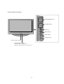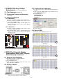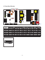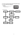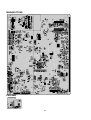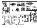
1
website:http://biz.LGservice.com
e-mail:http://www.LGEservice.com/techsup.html
PLASMA TV
SERVICE MANUAL
CHASSIS : PP62A
MODEL : 42PC3R
42PC3R-ZH
CAUTION
BEFORE SERVICING THE CHASSIS,
READ THE SAFETY PRECAUTIONS IN THIS MANUAL.
CONTENTS
SAFETY PRECAUTIONS ....................................................................................3
DESCRIPTION OF CONTROLS ..........................................................................4
SPECIFICATIONS ..............................................................................................10
ADJUSTMENT INSTRUCTIONS .......................................................................12
TROUBLE SHOOTING GUIDE ..........................................................................17
PRINTED CIRCUIT DIAGRAM ..........................................................................25
BLOCK DIAGRAM .............................................................................................27
EXPLODED VIEW ..............................................................................................28
EXPLODED VIEW PARTS LIST ........................................................................29
REPLACEMENT PARTS LIST...........................................................................30
SCHEMATIC DIAGRAM.........................................................................................
- 2 -
SAFETY PRECAUTIONS
IMPORTANT SAFETY NOTICE
Many electrical and mechanical parts in this chassis have special safety-related characteristics. These parts are identified by
in
the Schematic Diagram and Replacement Parts List.
It is essential that these special safety parts should be replaced with the same components as recommended in this manual to
prevent X-RADIATION, Shock, Fire, or other Hazards.
Do not modify the original design without permission of manufacturer.
Leakage Current Hot Check (See below Figure)
General Guidance
An isolation Transformer should always be used during
the servicing of a receiver whose chassis is not isolated from
the AC power line. Use a transformer of adequate power rating
as this protects the technician from accidents resulting in
personal injury from electrical shocks.
It will also protect the receiver and it's components from being
damaged by accidental shorts of the circuitry that may be
inadvertently introduced during the service operation.
If any fuse (or Fusible Resistor) in this monitor is blown, replace
it with the specified.
Plug the AC cord directly into the AC outlet.
Do not use a line Isolation Transformer during this check.
Connect 1.5K/10watt resistor in parallel with a 0.15uF capacitor
between a known good earth ground (Water Pipe, Conduit, etc.)
and the exposed metallic parts.
Measure the AC voltage across the resistor using AC
voltmeter with 1000 ohms/volt or more sensitivity.
Reverse plug the AC cord into the AC outlet and repeat AC
voltage measurements for each exposed metallic part. Any
voltage measured must not exceed 0.75 volt RMS which is
corresponds to 0.5mA.
In case any measurement is out of the limits specified, there is
possibility of shock hazard and the set must be checked and
repaired before it is returned to the customer.
When replacing a high wattage resistor (Oxide Metal Film
Resistor, over 1W), keep the resistor 10mm away from PCB.
Leakage Current Hot Check circuit
Keep wires away from high voltage or high temperature parts.
AC Volt-meter
Due to high vacuum and large surface area of picture tube,
extreme care should be used in handling the Picture Tube.
Do not lift the Picture tube by it's Neck.
Leakage Current Cold Check(Antenna Cold Check)
With the instrument AC plug removed from AC source,
connect an electrical jumper across the two AC plug prongs.
Place the AC switch in the on position, connect one lead of
ohm-meter to the AC plug prongs tied together and touch other
ohm-meter lead in turn to each exposed metallic parts such as
antenna terminals, phone jacks, etc.
If the exposed metallic part has a return path to the chassis, the
measured resistance should be between 1MΩ and 5.2MΩ.
When the exposed metal has no return path to the chassis the
reading must be infinite.
An other abnormality exists that must be corrected before the
receiver is returned to the customer.
- 3 -
To Instrument's
exposed
METALLIC PARTS
Good Earth Ground
such as WATER PIPE,
CONDUIT etc.
0.15uF
1.5 Kohm/10W
DESCRIPTION OF CONTROLS
POWER Switches the set on from standby or off to standby.
@@@@@@@@e?
@@@@@@@@e?@@@@@@@@e?@@@@@@@@?e@@@@@@@@e?@@@@@@@@?e@@@@@@@@e?@@@@@@@@?e@@@@@@@@e?@@@@@@@@?e@@@@@@@@e?@@@@@@@@?e@@@@@@@@e?@@@@@@@@?e@@@@@@@@e?@@@@@@@@?e@@@@@@@@e?@@@@@@@@?e@@@@@@@@e?@@@@@@@@?e@@@@@@@@e?@@@@@@@@?e@@@@@@@@e?@@@@@@@@?e@@@@@@@@e?@@@@@@@@?e@@@@@@@@e?@@@@@@@@?e
@@@@@@@@e?@@@@@@@@?e@@@@@@@@e?@@@@@@@@?e@@@@@@@@e?@@@@@@@@?e@@@@@@@@e?@@@@@@@@?e@@@@@@@@e?@@@@@@@@?e@@@@@@@@e?@@@@@@@@?e@@@@@@@@e?@@@@@@@@?e@@@@@@@@e?@@@@@@@@?e@@@@@@@@e?@@@@@@@@?e@@@@@@@@e?@@@@@@@@?e@@@@@@@@e?@@@@@@@@?e@@@@@@@@e?@@@@@@@@?e@@@@@@@@e?@@@@@@@@?e@@@@@@@@
@@@@@@@@
@@h?
@@
@@h?
@@
@@h?
@@
@@h?
@@
@@h?
@@
@@h?
@@
@@
@@
@@
@@
@@
@@
@@
@@
@@
@@
@@
@@
@@
@@
@@
@@
@@
@@
@@
@@
@@
@@
@@
@@
@@
@@
@@
@@
@@
@@
@@
@@
@@
@@
@@
@@
@@
@@
@@
@@
@@
@@
@@
@@
@@
@@
@@
@@
@@
@@
@@
@@
@@
@@
@@
@@
TV INPUT Returns from AV1, AV2, S-Video2, AV3, AV4(except
42PC3RV*), Component, RGB, HDMI1/DVI or
HDMI 2 to the TV mode. Switches the set on from
@@
@@
@@
@@
@@
@@
@@
@@
INPUT
TV
@@
@@
@@
@@
@@
@@
@@
@@
@@
@@
@@
@@
@@
@@
@@
@@
@@
@@
@@
@@
@@
@@
@@
@@
POWER
@@
@@
@@
@@
@@
@@
@@
@@
@@
@@
@@
@@
@@
@@
@@
@@
@@
@@
@@
@@
@@
@@
@@
@@
@@
@@
@@
@@
@@
@@
@@
@@
@@
@@
@@
@@
@@
@@
@@
@@
@@
@@
@@
@@
@@
@@
@@
@@
@@
@@
@@
@@
@@
@@
@@
@@
@@
@@
@@
@@
@@
@@
@@
@@
@@
@@
@@
@@
@@
@@
@@
@@
@@
@@
@@
@@
@@
@@
@@
@@
@@
@@
@@
@@
@@
@@
@@
@@
@@
@@
@@
@@
@@
@@
@@
@@
TV
@@
@@
@@
@@
@@
@@
@@
@@
@@
@@
@@
@@
@@
@@
@@
@@
@@
@@
@@
@@
@@
@@
@@
@@
INPUT
DVD
@@
@@
@@
@@
@@
@@
@@
@@
@@
@@
@@
@@
@@
@@
@@
@@
@@
@@
@@
@@
@@
@@
@@
@@
@@
@@
@@
@@
@@
@@
@@
@@
@@g
@@g
@@g
@@g
@@g
@@g
@@@@@@@@
@@@@@@@@ ?@@@@@@@@?e@@@@@@@@e?@@@@@@@@?e@@@@@@@@e?@@@@@@@@?e@@@@@@@@e?@@@@@@@@?e@@@@@@@@e?@@@@@@@@?e@@@@@@@@e?@@@@@@@@?e@@@@@@@@e?@@@@@@@@?e@@@@@@@@e?@@@@@@@@?e@@@@@@@@e?@@@@@@@@?e@@@@@@@@e?@@@@@@@@?e@@@@@@@@e?@@@@@@@@?e@@@@@@@@e?@@@@@@@@?e@@@@@@@@e?@@@@@@@@?e@@@@@@@@
?@@@@@@@@?e@@@@@@@@e?@@@@@@@@?e@@@@@@@@e?@@@@@@@@?e@@@@@@@@e?@@@@@@@@?e@@@@@@@@e?@@@@@@@@?e@@@@@@@@e?@@@@@@@@?e@@@@@@@@e?@@@@@@@@?e@@@@@@@@e?@@@@@@@@?e@@@@@@@@e?@@@@@@@@?e@@@@@@@@e?@@@@@@@@?e@@@@@@@@e?@@@@@@@@?e@@@@@@@@e?@@@@@@@@?e@@@@@@@@e?@@@@@@@@?e@@@@@@@@
?@@
?@@
?@@
?@@
?@@
?@@
?@@@@@@@@
?@@@@@@@@
@@@@@@@@e?
@@@@@@@@e?@@@@@@@@?e@@@@@@@@e?@@@@@@@@?e@@@@@@@@e?@@@@@@@@?e@@@@@@@@e?@@@@@@@@?e@@@@@@@@e?@@@@@@@@?e@@@@@@@@e?@@@@@@@@?e@@@@@@@@e?@@@@@@@@?e@@@@@@@@e?@@@@@@@@?e@@@@@@@@e?@@@@@@@@?e@@@@@@@@e?@@@@@@@@?e@@@@@@@@e?@@@@@@@@?e@@@@@@@@e?@@@@@@@@?e@@@@@@@@e?@@@@@@@@?e@@@@@@@@e?
@@@@@@@@e?
@@@@@@@@e?@@@@@@@@?e@@@@@@@@e?@@@@@@@@?e@@@@@@@@e?@@@@@@@@?e@@@@@@@@e?@@@@@@@@?e@@@@@@@@e?@@@@@@@@?e@@@@@@@@e?@@@@@@@@?e@@@@@@@@e?@@@@@@@@?e@@@@@@@@e?@@@@@@@@?e@@@@@@@@e?@@@@@@@@?e@@@@@@@@e?@@@@@@@@?e@@@@@@@@e?@@@@@@@@?e@@@@@@@@e?@@@@@@@@?e@@@@@@@@e?@@@@@@@@?e@@@@@@@@e?@@@@@@@@
@@@@@@@@
@@h?
@@
@@h?
@@
@@h?
@@
@@h?
@@
@@h?
@@
@@h?
@@
@@
@@
@@
@@
@@
@@
@@
@@
@@
@@
@@
@@
@@
@@
@@
@@
@@
@@
@@
@@
@@
@@
@@
@@
@@
@@
@@
@@
@@
@@
@@
@@
@@
@@
@@
@@
@@
@@
@@
@@
@@
@@
@@
@@
@@
@@
@@
@@
@@g
@@g
@@g
@@g
@@g
@@g
@@@@@@@@
@@@@@@@@
@@
@@
@@
@@
@@
@@
@@
@@
ARC
@@
@@
@@
@@
@@
@@
@@
@@
@@
@@
@@
@@
@@
@@
@@
@@
@@
@@
@@
@@
@@
@@
@@
@@
?@@@@@@@@?e@@@@@@@@e?@@@@@@@@?e@@@@@@@@e?@@@@@@@@?e@@@@@@@@e?@@@@@@@@?e@@@@@@@@e?@@@@@@@@?e@@@@@@@@e?@@@@@@@@?e@@@@@@@@e?@@@@@@@@?e@@@@@@@@e?@@@@@@@@?e@@@@@@@@e?@@@@@@@@?e@@@@@@@@e?@@@@@@@@?e@@@@@@@@e?@@@@@@@@?e@@@@@@@@e?@@@@@@@@?e@@@@@@@@e?@@@@@@@@?e@@@@@@@@e?@@@@@@@@
?@@@@@@@@?e@@@@@@@@e?@@@@@@@@?e@@@@@@@@e?@@@@@@@@?e@@@@@@@@e?@@@@@@@@?e@@@@@@@@e?@@@@@@@@?e@@@@@@@@e?@@@@@@@@?e@@@@@@@@e?@@@@@@@@?e@@@@@@@@e?@@@@@@@@?e@@@@@@@@e?@@@@@@@@?e@@@@@@@@e?@@@@@@@@?e@@@@@@@@e?@@@@@@@@?e@@@@@@@@e?@@@@@@@@?e@@@@@@@@e?@@@@@@@@?e@@@@@@@@e?@@@@@@@@
VCR
?@@
?@@
?@@
?@@
?@@
?@@
?@@@@@@@@
?@@@@@@@@
standby.
TEXT
INPUT If you press the button once, the input source OSD will
appear on screen as shown. Press the D / E button
and then OK button to select the desired input source
(TV, AV1, AV2, S-Video2, AV3, AV4(except 42PC3R*),
Component, RGB, HDMI1/DVI or HDMI 2).
PIP PR-
ARC Selects your desired picture format.
Brightness Adjusts screen brightness.
adjustment It returns to the default settings brightness by
changing mode source.
PIP
SIZE
POSTION
PIP PR+
SWAP
PIP INPUT
LIST
MENU
EXIT
I/II
SLEEP
OK
Coloured These buttons are used for teletext (only TELETEXT
buttons models) or Programme edit.
PIP Switches the sub picture PIP, DW, POP or off mode.
Q.VIEW
VOL
SIZE Adjusts the sub picture size.
PR
MUTE
POSITION Moves the sub picture.
PIP PR - /+ Selects a programme for the sub picture.
1
2
3
4
5
6
PIP INPUT Selects the input source for the sub picture in
PIP/Twin picture mode.
7
8
9
VCR/DVD Controls some video cassette recorders or DVD
when you have already selected DVD or
control buttons players
VCR mode button.
*
10
FAV
TIME
REVEAL
SWAP Exchanges the main/sub images in PIP/Twin picture
mode.
EXIT Clears all on-screen displays and returns to TV
viewing from any menu.
LIST Displays the programme table.
MENU Selects a menu.
I/II Selects the sound output.
SLEEP Sets the sleep timer.
- 4 -
?
INDEX
MODE Selects the remote operating modes.
INPUT
TV
@@@@@@@@e?
@@@@@@@@e?@@@@@@@@?e@@@@@@@@e?@@@@@@@@?e@@@@@@@@e?@@@@@@@@?e@@@@@@@@e?@@@@@@@@?e@@@@@@@@e?@@@@@@@@?e@@@@@@@@e?
@@@@@@@@e?
@@@@@@@@e?@@@@@@@@?e@@@@@@@@e?@@@@@@@@?e@@@@@@@@e?@@@@@@@@?e@@@@@@@@e?@@@@@@@@?e@@@@@@@@e?@@@@@@@@?e@@@@@@@@e?@@@@@@@@
@@@@@@@@
@@h?
@@
@@h?
@@
@@h?
@@
@@h?
@@
@@h?
@@
@@h?
@@
@@
@@
@@
@@
@@
@@
@@
@@
@@
@@
@@
@@
@@
@@
@@
@@
@@
@@
@@
@@
@@
@@
@@
@@
POWER
@@
@@
@@
@@
@@
@@
@@
@@
TV
@@
@@
@@
@@
@@
@@
@@
@@
@@
@@
@@
@@
@@
@@
@@
@@
@@
@@
@@
@@
@@
@@
@@
@@
@@
@@
@@
@@
@@
@@
@@
@@
@@
@@
@@
@@
@@
@@
@@
@@
@@
@@
@@
@@
@@
@@
@@
@@
@@
@@
@@
@@
@@
@@
@@
@@
@@
@@
@@
@@
@@
@@
@@
@@
@@
@@
@@
@@
@@
@@
@@
@@
@@
@@
@@
@@
@@
@@
@@
@@
@@
@@
@@
@@
@@
@@
@@
@@
@@
@@
@@
@@
@@
@@
@@
@@
1
@@
@@
@@
@@
@@
@@
@@
@@
@@
@@
@@
@@
@@
@@
@@
@@
TELETEXT These buttons are used for teletext.
BUTTONS For further details, see the ‘Teletext’ section.
@@
@@
@@
@@
@@
@@
@@
@@
INPUT
@@
@@
@@
@@
@@
@@
@@
@@
DVD
@@
@@
@@
@@
@@
@@
@@
@@
@@
@@
@@
@@
@@
@@
@@
@@
@@
@@
@@
@@
@@
@@
@@
@@
@@
@@
@@
@@
@@
@@
@@
@@
@@
@@
@@
@@
@@
@@
@@
@@
@@
@@
@@
@@
@@
@@
@@
@@
@@
@@
@@
@@
@@
@@
@@
@@
@@
@@
@@
@@
@@
@@
@@
@@
@@
@@
@@
@@
@@
@@
@@
@@
@@
@@
@@
@@
@@
@@
@@
@@
@@
@@
@@
@@
@@
@@
@@
@@
@@
@@
@@
@@
@@
@@
@@
@@
@@
@@
@@
@@
@@
@@
@@
@@
ARC
@@
@@
@@
@@
@@
@@
@@
@@
@@
@@
@@
@@
@@
@@
@@
@@
@@
@@
@@
@@
@@
@@
@@
@@
@@
@@
@@
@@
@@
@@
@@
@@
VCR
@@
@@
@@
@@
@@
@@
@@
@@
@@
@@
@@
@@
@@
@@
@@
@@
@@
@@
@@
@@
@@
@@
@@
@@
@@g
@@g
@@g
@@g
@@g
@@g
@@@@@@@@
@@@@@@@@ ?@@@@@@@@?e@@@@@@@@e?@@@@@@@@?e@@@@@@@@e?@@@@@@@@?e@@@@@@@@e?@@@@@@@@?e@@@@@@@@e?@@@@@@@@?e@@@@@@@@e?@@@@@@@@
?@@@@@@@@?e@@@@@@@@e?@@@@@@@@?e@@@@@@@@e?@@@@@@@@?e@@@@@@@@e?@@@@@@@@?e@@@@@@@@e?@@@@@@@@?e@@@@@@@@e?@@@@@@@@
?@@
?@@
?@@
?@@
?@@
?@@
?@@@@@@@@
?@@@@@@@@
@@@@@@@@e?
@@@@@@@@e?@@@@@@@@?e@@@@@@@@e?@@@@@@@@?e@@@@@@@@e?@@@@@@@@?e@@@@@@@@e?@@@@@@@@?e@@@@@@@@e?@@@@@@@@?e@@@@@@@@e?@@@@@@@@?e@@@@@@@@e?@@@@@@@@?e@@@@@@@@e?@@@@@@@@?e@@@@@@@@e?@@@@@@@@?e@@@@@@@@e?@@@@@@@@?e@@@@@@@@e?@@@@@@@@?e@@@@@@@@e?@@@@@@@@?e@@@@@@@@e?@@@@@@@@?e@@@@@@@@e?@@@@@@@@?e@@@@@@@@e?@@@@@@@@?e@@@@@@@@e?@@@@@@@@?e@@@@@@@@e?@@@@@@@@?e@@@@@@@@e?@@@@@@@@?e@@@@@@@@e?@@@@@@@@?e@@@@@@@@e?@@@@@@@@
@@@@@@@@e?
@@h?@@@@@@@@e?@@@@@@@@?e@@@@@@@@e?@@@@@@@@?e@@@@@@@@e?@@@@@@@@?e@@@@@@@@e?@@@@@@@@?e@@@@@@@@e?@@@@@@@@?e@@@@@@@@e?@@@@@@@@?e@@@@@@@@e?@@@@@@@@?e@@@@@@@@e?@@@@@@@@?e@@@@@@@@e?@@@@@@@@?e@@@@@@@@e?@@@@@@@@?e@@@@@@@@e?@@@@@@@@?e@@@@@@@@e?@@@@@@@@?e@@@@@@@@e?@@@@@@@@?e@@@@@@@@e?@@@@@@@@?e@@@@@@@@e?@@@@@@@@?e@@@@@@@@e?@@@@@@@@?e@@@@@@@@e?@@@@@@@@?e@@@@@@@@e?@@@@@@@@?e@@@@@@@@e?@@@@@@@@?e@@@@@@@@e?@@@@@@@@
@@
@@h?
@@
@@h?
@@
@@h?
@@
@@h?
@@
@@h?
@@
@@
@@
@@
@@
@@
@@
@@
@@
@@
@@
@@
@@
@@
@@
@@
@@
@@
@@
@@
@@
@@
@@
@@
@@
@@
@@
@@
@@
@@
@@
@@
@@
@@
@@
@@
@@
@@
@@
@@
@@
TEXT
@@
@@
@@
@@
@@
@@
@@
@@
@@
@@
@@
@@
@@
@@
@@
@@
@@
@@
@@
@@
@@
@@
@@
@@
@@
@@
@@
@@
@@
@@
@@
@@
PIP
SIZE
POSTION
PIP PR+
SWAP
PIP INPUT
@@
@@
@@
@@
@@
@@
@@
@@
@@
@@
@@
@@
@@
@@
@@
@@
@@
@@
@@
@@
@@
@@
@@
@@
@@
@@
@@
@@
@@
@@
@@
@@
1
@@
@@
@@
@@
@@
@@
@@
@@
@@
@@
@@
@@
@@
@@
@@
@@
@@
@@
@@
@@
@@
@@
@@
@@
@@
@@
@@
@@
@@
@@
@@
@@
PIP PR-
@@
@@
@@
@@
@@
@@
@@
@@
THUMBSTICK Allows you to navigate the on-screen menus and
(Up/Down/Left adjust the system settings to your preference.
Right/ENTER)
@@
@@
@@
@@
@@
@@
@@
@@
@@
@@
@@
@@
@@
@@
@@
@@
@@
@@
@@
@@
@@
@@
@@
@@
@@
@@
@@
@@
@@
@@
@@
@@
@@
@@
@@
@@
@@
@@
@@
@@
@@
@@
@@
@@
@@
@@
@@
@@
@@
@@
@@
@@
@@
@@
@@
@@
@@
@@
@@
@@
@@
@@
@@
@@
@@
@@
@@
@@
@@
@@
@@
@@
@@
@@
@@
@@
@@
@@
@@
@@
@@
@@
@@
@@
@@
@@
@@
@@
@@
@@
@@
@@
@@
@@
@@
@@
@@
@@
@@
@@
@@
@@
@@
@@
@@
@@
@@
@@
@@
@@
@@
@@
@@g
@@g
@@g
@@g
@@g
@@g
@@@@@@@@
@@@@@@@@
?@@@@@@@@?e@@@@@@@@e?@@@@@@@@?e@@@@@@@@e?@@@@@@@@?e@@@@@@@@e?@@@@@@@@?e@@@@@@@@e?@@@@@@@@?e@@@@@@@@e?@@@@@@@@?e@@@@@@@@e?@@@@@@@@?e@@@@@@@@e?@@@@@@@@?e@@@@@@@@e?@@@@@@@@?e@@@@@@@@e?@@@@@@@@?e@@@@@@@@e?@@@@@@@@?e@@@@@@@@e?@@@@@@@@?e@@@@@@@@e?@@@@@@@@?e@@@@@@@@e?@@@@@@@@?e@@@@@@@@e?@@@@@@@@?e@@@@@@@@e?@@@@@@@@?e@@@@@@@@e?@@@@@@@@?e@@@@@@@@e?@@@@@@@@?e@@@@@@@@e?@@@@@@@@?e@@@@@@@@e?@@@@@@@@
?@@@@@@@@?e@@@@@@@@e?@@@@@@@@?e@@@@@@@@e?@@@@@@@@?e@@@@@@@@e?@@@@@@@@?e@@@@@@@@e?@@@@@@@@?e@@@@@@@@e?@@@@@@@@?e@@@@@@@@e?@@@@@@@@?e@@@@@@@@e?@@@@@@@@?e@@@@@@@@e?@@@@@@@@?e@@@@@@@@e?@@@@@@@@?e@@@@@@@@e?@@@@@@@@?e@@@@@@@@e?@@@@@@@@?e@@@@@@@@e?@@@@@@@@?e@@@@@@@@e?@@@@@@@@?e@@@@@@@@e?@@@@@@@@?e@@@@@@@@e?@@@@@@@@?e@@@@@@@@e?@@@@@@@@?e@@@@@@@@e?@@@@@@@@?e@@@@@@@@e?@@@@@@@@?e@@@@@@@@e?@@@@@@@@
?@@
?@@
?@@
?@@
?@@
?@@
?@@@@@@@@
?@@@@@@@@
OK Accepts your selection or displays the current mode.
VOLUME UP Adjusts the volume.
/DOWN
LIST
MENU
EXIT
I/II
SLEEP
Q.VIEW Returns to the previously viewed programme.
MUTE Switches the sound on or off.
OK
Programme Selects available programmes.
UP/DOWN
0~9 number Selects a programme.
button
Selects numbered items in a menu.
@@@@@@@@e?
@@@@@@@@e?@@@@@@@@?e@@@@@@@@e?@@@@@@@@?e@@@@@@@@e?@@@@@@@@?e@@@@@@@@e?@@@@@@@@?e@@@@@@@@e?@@@@@@@@?e@@@@@@@@e?@@@@@@@@?e@@@@@@@@e?@@@@@@@@?e@@@@@@@@e?@@@@@@@@?e@@@@@@@@e?@@@@@@@@?e@@@@@@@@e?@@@@@@@@?e@@@@@@@@e?@@@@@@@@?e@@@@@@@@e?@@@@@@@@?e@@@@@@@@e?@@@@@@@@?e@@@@@@@@e?@@@@@@@@?e@@@@@@@@e?@@@@@@@@?e@@@@@@@@e?@@@@@@@@?e@@@@@@@@e?@@@@@@@@?e@@@@@@@@e?@@@@@@@@?e@@@@@@@@e?@@@@@@@@?e@@@@@@@@e?
@@@@@@@@e?
@@@@@@@@e?@@@@@@@@?e@@@@@@@@e?@@@@@@@@?e@@@@@@@@e?@@@@@@@@?e@@@@@@@@e?@@@@@@@@?e@@@@@@@@e?@@@@@@@@?e@@@@@@@@e?@@@@@@@@?e@@@@@@@@e?@@@@@@@@?e@@@@@@@@e?@@@@@@@@?e@@@@@@@@e?@@@@@@@@?e@@@@@@@@e?@@@@@@@@?e@@@@@@@@e?@@@@@@@@?e@@@@@@@@e?@@@@@@@@?e@@@@@@@@e?@@@@@@@@?e@@@@@@@@e?@@@@@@@@?e@@@@@@@@e?@@@@@@@@?e@@@@@@@@e?@@@@@@@@?e@@@@@@@@e?@@@@@@@@?e@@@@@@@@e?@@@@@@@@?e@@@@@@@@e?@@@@@@@@?e@@@@@@@@e?@@@@@@@@
@@@@@@@@
@@h?
@@
@@h?
@@
@@h?
@@
@@h?
@@
@@h?
@@
@@h?
@@
@@
@@
@@
@@
@@
@@
@@
@@
@@
@@
@@
@@
@@
@@
@@
@@
@@
@@
@@
@@
@@
@@
@@
@@
@@
@@
@@
@@
@@
@@
@@
@@
@@
@@
@@
@@
@@
@@
@@
@@
@@
@@
@@
@@
@@
@@
@@
@@
@@
@@
@@
@@
@@
@@
@@
@@
@@
@@
@@
@@
@@
@@
@@
@@
@@
@@
@@
@@
@@
@@
@@
@@
@@
@@
@@
@@
@@
@@
@@
@@
@@
@@
@@
@@
@@
@@
@@
@@
@@
@@
@@
@@
@@
@@
@@
@@
@@
@@
@@
@@
@@
@@
@@
@@
@@
@@
@@
@@
@@
@@
@@
@@
@@
@@
@@
@@
@@
@@
@@
@@
VOL
@@
@@
@@
@@
@@
@@
@@
@@
@@
@@
@@
@@
@@
@@
@@
@@
FAV Displays the selected favourite programme.
PR
@@
@@
@@
@@
@@
@@
@@
@@
@@
@@
@@
@@
@@
@@
@@
@@
@@
@@
@@
@@
@@
@@
@@
@@
@@
@@
@@
@@
@@
@@
@@
@@
@@
@@
@@
@@
@@
@@
@@
@@
@@
@@
@@
@@
@@
@@
@@
@@
@@
@@
@@
@@
@@
@@
@@
@@
@@
@@
@@
@@
@@
@@
@@
@@
@@
@@
@@
@@
@@
@@
@@
@@
MUTE
@@
@@
@@
@@
@@
@@
@@
@@
No function
@@
@@
@@
@@
@@
@@
@@
@@
@@
@@
@@
@@
@@
@@
@@
@@
@@
@@
@@
@@
@@
@@
@@
@@
@@
@@
@@
@@
@@
@@
@@
@@
*
@@
@@
@@
@@
@@
@@
@@
@@
Q.VIEW
@@
@@
@@
@@
@@
@@
@@
@@
@@
@@
@@
@@
@@
@@
@@
@@
@@
@@
@@
@@
@@
@@
@@
@@
@@
@@
@@
@@
@@
@@
@@
@@
@@
@@
@@
@@
@@
@@
@@
@@
@@
@@
@@
@@
@@
@@
@@
@@
@@
@@
@@
@@
@@
@@
@@
@@
@@
@@
@@
@@
@@
@@
@@
@@
@@
@@
@@
@@
@@
@@
@@
@@
@@
@@
@@
@@
@@
@@
@@
@@
@@
@@
@@
@@
@@
@@
@@
@@
@@
@@
@@
@@
@@
@@
@@
@@
@@
@@
@@
@@
@@
@@
@@
@@
@@
@@
@@
@@
@@
@@
@@
@@
@@
@@
@@
@@
@@
@@
@@
@@
@@
@@
@@
@@
@@
@@
@@
@@
@@
@@
@@
@@
@@
@@
@@
@@
@@
@@
@@
@@
@@
@@
@@
@@
@@
@@
@@
@@
@@
@@
@@
@@
1
@@
@@
@@
@@
@@
@@
@@
@@
@@
@@
@@
@@
@@
@@
@@
@@
@@
@@
@@
@@
@@
@@
@@
@@
2
3
@@
@@
@@
@@
@@
@@
@@
@@
@@
@@
@@
@@
@@
@@
@@
@@
@@
@@
@@
@@
@@
@@
@@
@@
@@
@@
@@
@@
@@
@@
@@
@@
@@
@@
@@
@@
@@
@@
@@
@@
@@
@@
@@
@@
@@
@@
@@
@@
@@
@@
@@
@@
@@
@@
@@
@@
@@
@@
@@
@@
@@
@@
@@
@@
@@
@@
@@
@@
@@
@@
@@
@@
@@
@@
@@
@@
@@
@@
@@
@@
@@
@@
@@
@@
@@
@@
@@
@@
@@
@@
@@
@@
@@
@@
@@
@@
@@
@@
@@
@@
@@
@@
@@
@@
@@
@@
@@
@@
@@
@@
@@
@@
@@
@@
@@
@@
@@
@@
@@
@@
4
@@
@@
@@
@@
@@
@@
@@
@@
@@
@@
@@
@@
@@
@@
@@
@@
@@
@@
@@
@@
@@
@@
@@
@@
5
6
@@
@@
@@
@@
@@
@@
@@
@@
@@
@@
@@
@@
@@
@@
@@
@@
@@
@@
@@
@@
@@
@@
@@
@@
@@
@@
@@
@@
@@
@@
@@
@@
@@
@@
@@
@@
@@
@@
@@
@@
@@
@@
@@
@@
@@
@@
@@
@@
@@
@@
@@
@@
@@
@@
@@
@@
@@
@@
@@
@@
@@
@@
@@
@@
@@
@@
@@
@@
@@
@@
@@
@@
@@
@@
@@
@@
@@
@@
@@
@@
@@
@@
@@
@@
@@
@@
@@
@@
@@
@@
@@
@@
@@
@@
@@
@@
@@
@@
@@
@@
@@
@@
@@
@@
@@
@@
@@
@@
@@
@@
@@
@@
@@
@@
@@
@@
@@
@@
@@
@@
7
@@
@@
@@
@@
@@
@@
@@
@@
@@
@@
@@
@@
@@
@@
@@
@@
@@
@@
@@
@@
@@
@@
@@
@@
8
9
@@
@@
@@
@@
@@
@@
@@
@@
@@
@@
@@
@@
@@
@@
@@
@@
@@
@@
@@
@@
@@
@@
@@
@@
@@
@@
@@
@@
@@
@@
@@
@@
@@
@@
@@
@@
@@
@@
@@
@@
@@
@@
@@
@@
@@
@@
@@
@@
@@
@@
@@
@@
@@
@@
@@
@@
@@
@@
@@
@@
@@
@@
@@
@@
@@
@@
@@
@@
@@
@@
@@
@@
@@
@@
@@
@@
@@
@@
@@
@@
@@
@@
@@
@@
@@
@@
@@
@@
@@
@@
@@
@@
@@
@@
@@
@@
@@
@@
@@
@@
@@
@@
@@
@@
@@
@@
@@
@@
@@
@@
@@
@@
@@
@@
@@
@@
@@
@@
@@
@@
*
@@
@@
@@
@@
@@
@@
@@
@@
@@
@@
@@
@@
@@
@@
@@
@@
@@
@@
@@
@@
@@
@@
@@
@@
@@
@@
@@
@@
@@
@@
@@
@@
@@
@@
@@
@@
@@
@@
@@
@@
@@g
@@g
@@g
@@g
@@g
@@g
@@@@@@@@
@@@@@@@@
10
FAV
@@
@@
@@
@@
@@
@@
@@
@@
@@
@@
@@
@@
@@
@@
@@
@@
@@
@@
@@
@@
@@
@@
@@
@@
@@
@@
@@
@@
@@
@@
@@
@@
@@
@@
@@
@@
@@
@@
@@
@@
@@
@@
@@
@@
@@
@@
@@
@@
?@@@@@@@@?e@@@@@@@@e?@@@@@@@@?e@@@@@@@@e?@@@@@@@@?e@@@@@@@@e?@@@@@@@@?e@@@@@@@@e?@@@@@@@@?e@@@@@@@@e?@@@@@@@@?e@@@@@@@@e?@@@@@@@@?e@@@@@@@@e?@@@@@@@@?e@@@@@@@@e?@@@@@@@@?e@@@@@@@@e?@@@@@@@@?e@@@@@@@@e?@@@@@@@@?e@@@@@@@@e?@@@@@@@@?e@@@@@@@@e?@@@@@@@@?e@@@@@@@@e?@@@@@@@@?e@@@@@@@@e?@@@@@@@@?e@@@@@@@@e?@@@@@@@@?e@@@@@@@@e?@@@@@@@@?e@@@@@@@@e?@@@@@@@@?e@@@@@@@@e?@@@@@@@@?e@@@@@@@@e?@@@@@@@@
?@@@@@@@@?e@@@@@@@@e?@@@@@@@@?e@@@@@@@@e?@@@@@@@@?e@@@@@@@@e?@@@@@@@@?e@@@@@@@@e?@@@@@@@@?e@@@@@@@@e?@@@@@@@@?e@@@@@@@@e?@@@@@@@@?e@@@@@@@@e?@@@@@@@@?e@@@@@@@@e?@@@@@@@@?e@@@@@@@@e?@@@@@@@@?e@@@@@@@@e?@@@@@@@@?e@@@@@@@@e?@@@@@@@@?e@@@@@@@@e?@@@@@@@@?e@@@@@@@@e?@@@@@@@@?e@@@@@@@@e?@@@@@@@@?e@@@@@@@@e?@@@@@@@@?e@@@@@@@@e?@@@@@@@@?e@@@@@@@@e?@@@@@@@@?e@@@@@@@@e?@@@@@@@@?e@@@@@@@@e?@@@@@@@@
?@@
?@@
?@@
?@@
?@@
?@@
?@@@@@@@@
?@@@@@@@@
@@@@@@@@e?
@@@@@@@@e?@@@@@@@@?e@@@@@@@@e?@@@@@@@@?e@@@@@@@@e?@@@@@@@@?e@@@@@@@@e?@@@@@@@@?e@@@@@@@@e?@@@@@@@@?e@@@@@@@@e?@@@@@@@@?e@@@@@@@@e?@@@@@@@@?e@@@@@@@@e?@@@@@@@@?e@@@@@@@@e?@@@@@@@@?e@@@@@@@@e?@@@@@@@@?e@@@@@@@@e?@@@@@@@@?e@@@@@@@@e?@@@@@@@@?e@@@@@@@@e?@@@@@@@@?e@@@@@@@@e?@@@@@@@@?e@@@@@@@@e?@@@@@@@@?e@@@@@@@@e?@@@@@@@@?e@@@@@@@@e?@@@@@@@@?e@@@@@@@@e?@@@@@@@@?e@@@@@@@@e?@@@@@@@@?e@@@@@@@@e?
@@@@@@@@e?
@@@@@@@@e?@@@@@@@@?e@@@@@@@@e?@@@@@@@@?e@@@@@@@@e?@@@@@@@@?e@@@@@@@@e?@@@@@@@@?e@@@@@@@@e?@@@@@@@@?e@@@@@@@@e?@@@@@@@@?e@@@@@@@@e?@@@@@@@@?e@@@@@@@@e?@@@@@@@@?e@@@@@@@@e?@@@@@@@@?e@@@@@@@@e?@@@@@@@@?e@@@@@@@@e?@@@@@@@@?e@@@@@@@@e?@@@@@@@@?e@@@@@@@@e?@@@@@@@@?e@@@@@@@@e?@@@@@@@@?e@@@@@@@@e?@@@@@@@@?e@@@@@@@@e?@@@@@@@@?e@@@@@@@@e?@@@@@@@@?e@@@@@@@@e?@@@@@@@@?e@@@@@@@@e?@@@@@@@@?e@@@@@@@@e?@@@@@@@@
@@@@@@@@
@@h?
@@
@@h?
@@
@@h?
@@
@@h?
@@
@@h?
@@
@@h?
@@
@@
@@
@@
@@
@@
@@
@@
@@
1
@@
@@
@@
@@
@@
@@
@@
@@
?
@@
@@
@@
@@
@@
@@
@@
@@
@@
@@
@@
@@
@@
@@
@@
@@
@@
@@
@@
@@
@@
@@
@@
@@
@@
@@
@@
@@
@@
@@
@@
@@
@@
@@
@@
@@
@@
@@
@@
@@
@@
@@
@@
@@
@@
@@
@@
@@
@@
@@
@@
@@
@@
@@
@@
@@
TIME
REVEAL
INDEX
@@
@@
@@
@@
@@
@@
@@
@@
@@
@@
@@
@@
@@
@@
@@
@@
@@
@@
@@
@@
@@
@@
@@
@@
- 5 -
@@
@@
@@
@@
@@
@@
@@
@@
@@
@@
@@
@@
@@
@@
@@
@@
@@
@@
@@
@@
@@
@@
@@
@@
@@g
@@g
@@g
@@g
@@g
@@g
@@@@@@@@
@@@@@@@@
@@
@@
@@
@@
@@
@@
@@
@@
@@
@@
@@
@@
@@
@@
@@
@@
@@
@@
@@
@@
@@
@@
@@
@@
?@@@@@@@@?e@@@@@@@@e?@@@@@@@@?e@@@@@@@@e?@@@@@@@@?e@@@@@@@@e?@@@@@@@@?e@@@@@@@@e?@@@@@@@@?e@@@@@@@@e?@@@@@@@@?e@@@@@@@@e?@@@@@@@@?e@@@@@@@@e?@@@@@@@@?e@@@@@@@@e?@@@@@@@@?e@@@@@@@@e?@@@@@@@@?e@@@@@@@@e?@@@@@@@@?e@@@@@@@@e?@@@@@@@@?e@@@@@@@@e?@@@@@@@@?e@@@@@@@@e?@@@@@@@@?e@@@@@@@@e?@@@@@@@@?e@@@@@@@@e?@@@@@@@@?e@@@@@@@@e?@@@@@@@@?e@@@@@@@@e?@@@@@@@@?e@@@@@@@@e?@@@@@@@@?e@@@@@@@@e?@@@@@@@@
?@@@@@@@@?e@@@@@@@@e?@@@@@@@@?e@@@@@@@@e?@@@@@@@@?e@@@@@@@@e?@@@@@@@@?e@@@@@@@@e?@@@@@@@@?e@@@@@@@@e?@@@@@@@@?e@@@@@@@@e?@@@@@@@@?e@@@@@@@@e?@@@@@@@@?e@@@@@@@@e?@@@@@@@@?e@@@@@@@@e?@@@@@@@@?e@@@@@@@@e?@@@@@@@@?e@@@@@@@@e?@@@@@@@@?e@@@@@@@@e?@@@@@@@@?e@@@@@@@@e?@@@@@@@@?e@@@@@@@@e?@@@@@@@@?e@@@@@@@@e?@@@@@@@@?e@@@@@@@@e?@@@@@@@@?e@@@@@@@@e?@@@@@@@@?e@@@@@@@@e?@@@@@@@@?e@@@@@@@@e?@@@@@@@@
?@@
?@@
?@@
?@@
?@@
?@@
?@@@@@@@@
?@@@@@@@@
Front Panel Controls
PROGRAMME Buttons
PR
VOLUME Buttons
VOL
OK
OK Button
MENU
MENU Button
INPUT
INPUT Button
ON/OFF Button
Remote Control Sensor
Power/Standby Indicator
• illuminates red in standby mode.
• illuminates white when the set is switched on.
- 6 -
Back Connection Panel
AUDIO Input
Connections are available for listening stereo sound from an external
device.
AV IN 4
R
AUDIO
L/MONO
VIDEO Input
Connects the video signal from a
video device.
(except 42PC3RV*)
VIDEO
1
2
3
AV 1
4
AV 2
AC IN
VARIABLE
AUDIO OUT
RGB IN
RGB IN
(PC/DTV)
HDMI IN
AUDIO
(RGB/DVI)
2
COMPONENT IN
AV IN 3
1 (DVI)
RS-232C IN
(CONTROL & SERVICE)
REMOTE
CONTROL IN
ANTENNA
IN
(MONO)
S-VIDEO
5
6
7
8
VIDEO
VIDEO
AUDIO
9
AUDIO
10
11
6
Variable Audio Output
Connect an external amplifier or add a subwoofer to your surround sound system.
HDMI Input
Connect a HDMI signal to HDMI IN.
Connect DVI(VIDEO) signal to HDMI/DVI
port with DVI to HDMI cable.
7
3
Euro Scart Socket (AV1/AV2)
Connect scart socket input or output from
an external device to these jacks.
RS-232C Input(CONTROL&SERVICE)Port
Connect the serial port of the control
devices to the RS-232C jack.
8
4
Power Cord Socket
This TV operates on an AC power. The
voltage is indicated on the Specifications
page. Never attempt to operate the TV on
DC power.
S-Video Input
Connect S-Video out from an S-VIDEO
device.
9
Audio/Video Input
Connect audio/video output from an external device to these jacks.
1
RGB/Audio Input
Connect the monitor output from a PC/DTV
to the appropriate input port.
2
5
10
Component Input
Connect a component video/audio device
to these jacks.
Remote Control Port
11
- 7 -
Antenna Input
ACCESSORIES
INPUT
TV
TV
POWER
INPUT
DVD
ARC
VCR
TEXT
PIP PR-
PIP
SIZE
POSTION
PIP PR+
SWAP
PIP INPUT
LIST
MENU
EXIT
I/II
SLEEP
OK
Owner’s Manual
Q.VIEW
VOL
PR
MUTE
1
2
4
5
3
6
7
8
9
*
10
FAV
?
TIME
Owner’s Manual
Batteries
REVEAL
INDEX
Remote Control
Power Cord
Polishing Cloth
Polish the screen with the cloth
(Option)
For 42PC1R*, 42PC3R*, 50PC1R*
2-Wall brackets
2-bolts for stand assembly
2-eye-bolts
- 8 -
STAND INSTALLATION(OPTION)
1
2
A
3
4
B
C
O Place
the set with the screen facing down on a cushion or soft cloth as shown in Figures 1.
Before unfolding the stand, please make sure two locks (A) on the bottom of the stand push outward.
O Pull the stand out as shown above in Figures 2 ~ 3.
After unfolding the stand, please insert and tighten the screws in the holes (B) on the bottom of the
stand.
O When connecting cables to the set, Do not disengage the lock (C).
This may cause the set to fall, causing serious bodily injury and serious damage to the set.
* NOTE
Figures shown here may be slightly different from your set.
When closing the stand for storage
First remove the screws in the holes (B) on the bottom
of the stand. And then pull two Hooks (D) of the stand
bottom
and fold the stand into the back of the set.
After folding, push two Locks (A) of the stand bottom
outward.
- 9 -
D
A
B
SPECIFICATIONS
NOTE : Specifications and others are subject to change without notice for improvement.
V
Application Range
This spec is applied to the 42” PLASMA TV used PP62A Chassis.
V
Chassis
Model Name
Market
Brand
PP62A
42PC3R-ZH
EU
LG
Remark
Specification
Each part is tested as below without special appointment.
1) Temperature : 25±5°C (77±9°F), CST : 40±5
2) Relative Humidity: 65±10%.
3) Power Voltage: Standard Input voltage (100-240V~, 50/60Hz).
* Standard Voltage of each product is marked by models.
4) Specification and performance of each parts are followed each drawing and specification by part number in accordance with BOM.
5) The receiver must be operated for about 20 minutes prior to the adjustment.
V
Test Method
1) Performance : LGE TV test method followed.
2) Demanded other specification .
Safety : CE, IEC specification
EMC : CE, IEC
V
Model
Market
42PC3R-ZH
EU
Appliance
Remark
Safety : IEC/EN60065, EMI : EN55013, EMS : EN55020
TEST
General Specification
1. Module Specification
1-1. 42”XGA MODULE
No
Item
Specification
1
Display Screen Device
42” Wide Color Display Module
2
Aspect Ratio
16:9
3
PDP Module
PDP42X3,
Remark
Plasma Display Panel
Clear Filter
RGB Closed Type
4
Operating Environment
1)Temp.
: 0~40deg
LGE SPEC.
2)Humidity : 0~85%
5
Storage Environment
3)Temp.
: -20~60deg
4)Humidity : 0~85%
6
Input Voltage
100-240V~, 50/60Hz
- 10 -
Maker : LG
1-2. 42”WVGA MODULE
No
Item
Specification
1
Display Screen Device
42” Wide Color Display Module
2
Aspect Ratio
16:9
3
PDP Module
PDP42V8,
Remark
Plasma Display Panel
Clear Filter
RGB Closed Type
4
Operating Environment
1)Temp.
LGE SPEC.
: 0~40deg
2)Humidity : 0~85%
5
Storage Environment
3)Temp.
: -20~60deg
4)Humidity : 0~85%
6
Input Voltage
100-240V~, 50/60Hz
Maker : Sanken
2. Model General Specification
No
Item
Specification
1
Market
EU
2
Broadcasting system
PAL-BG/I/DK, SECAM
BAND
3
Available Channel
PAL
VHF
E2~E12
UHF
E21~E69
CATV
S1~S20
HYPER
S21~S47
Remark
SECAM
4
Receiving system
Upper Heterodyne
5
Scart Jack (2EA)
PAL, SECAM, NTSC,NTSC4.43
4 System : PAL, SECAM, NTSC, PAL60
6
Video Input (1EA)
PAL, SECAM, NTSC,NTSC4.43
4 System : PAL, SECAM, NTSC, PAL60
7
S-Video Input (2EA)
PAL, SECAM, NTSC,NTSC4.43
4 System : PAL, SECAM, NTSC, PAL60
8
Component Input (1EA)
Y/Cb/Cr, Y/Pb/Pr
9
RGB Input (1EA)
RGB-PC,
RGB-DTV
10
HDMI Input (2EA)
HDMI-PC
HDMI-DTV
11
Audio Input (3EA)
12
Wired Control (1EA)
13
Audio variable out (1EA)
PC Audio, Component(1EA), AV (1EA)
- 11 -
L/R Input
ADJUSTMENT INSTRUCTIONS
3-2. Channel memory Method
1. Application Object
These instructions is applied all of the 42” PLASMA TV,
PP62A Chassis.
2. Notes
(1) Because this is not a hot chassis, it is not necessary to use
an isolation transformer. However, the use of isolation
transformer will help protect test instrument.
(2) Adjustment must be done in the correct order.
(3) The adjustment must be performed in the circumstance of
25±5°C of temperature and 65±10% of relative humidity if
there is no specific designation.
(4) The input voltage of the receiver must keep 100-220V~,
50/60Hz.
(5) The receiver must be operated for about 15 minutes prior
to the adjustment.
1) Select “PDP” and “Hurricane” on Model dialog. And check
your connection in Communication dialog. (If your
connection is ‘NG’, then set your PORT(COM1,2,3,...)
correctly.)
2) Connect RS-232C cable and turn on the power.
(If your connection has completed, you can see “Ready”.)
[ If your set is not an end products but only a board, you
have to make your board to Stand-by state (LED_R). And
you have to Download in Stand_by power state.
(1)
After RGB Full white HEAT-RUN Mode, the receiver must
be operated prior to adjustment.
O Enter into HEAT-RUN MODE.
1) Press the POWER ON KEY on R/C for adjustment.
2) OSD display and screen display PATTERN MODE.
O
(2)
[ Set is activated HEAT-RUN without signal generator in
this mode.
[ Single color pattern(RED/BLUE/GREEN) of HEAT-RUN
mode uses to check PANEL.
(Fig. 2)
Caution) If you turn on a still screen more than 20 minutes,
(Especially digital pattern, cross hatch pattern) after
image may be occur in the black level part of the screen.
3. Channel memory
3-1. Setting up the LGIDS
1) Install the LGIDS. (idsinst.exe)
2) After installation, restart your PC.
3) Extract [files.zip] to folder [c:\LGIDS\files].
4) Start LGIDS.
3) Select proper CH_memory file(*.nvm) for each model at
[NVRAM Download] $ [Write Batch]
Next, select proper binary file(*.bin) including the CH
information for each model at [NVRAM File].
File name
ZH Model : H3_CH_Memory_ZH.nvm
4) Click the [Download] button.
It means the completion of the CH memory download if all
items show ‘OK’ and Status is changed by ‘PASS’ at the
lower right corner of the window.
5) If you want to check whether the CH information is
memorized correctly or not, click the [Verify] button.
And then compare NVRAM File(*.bin) with the CH
information downloaded.
(3)
(4)
(Fig. 3)
(Fig. 1)
- 12 -
5-3. Method of Auto RGB Color Balance
4. Auto AV(CVBS) Color Balance
1) Input the Component 720p 100% Color Bar signal into
Component1 or Component2.
2) Set the PSM to Dynamic mode in Picture menu.
3) Press INSTART key on R/C for adjustment.
4) Press the G (Vol.+) key operate To set , then it becomes
automatically.
5) Auto-RGB OK means completed adjustment.
4-1. Requirement
O
It is very import to use correct adjustment pattern like (Fig.4).
A Within the pattern, color sequence should be aligned :
W-Y-C-G-M-R-BLUE-BLACK.
(If color sequence is reversed (Black ->...-> White),
reverse the pattern with REV key, when using Master
pattern generator like MSPG-925)
A If Minimum Black Level and/or Maximum White Level is
not correct, Do select 100% Color Bar Pattern.
4-2. Required Test Equipment
1) Remote controller for adjustment.
2) AV Pattern Generator : 802F Pattern Generator,
Master(MSPG-925FA), etc.
(Which has PAL Composite Video format output with
standard(1.0 Vpp) Vertical 100% Color Bar Pattern as Fig. 4.)
4-3. Method of Auto RGB Color Balance
(Fig. 5) Auto Component Color Balance Test Pattern
1) Input the PAL Composite Video (Fig.4. 100% Color Bar
Pattern) into video input.
2) If Assy has Scart jack ,Use AV3
Else use AV1.
3) Press INSTART key on R/C for adjustment.
4) Press the G (Vol.+) key operate to set , then it becomes
automatically.
5) Auto-RGB OK means completed adjustment.
6. Auto RGB Color Balance
6-1. Requirement
O
It is very import to use correct adjustment pattern like (Fig.6).
A Within the pattern, color sequence should be aligned :
W-Y-C-G-M-R-BLUE-BLACK.
(If color sequence is reversed (Black ->...-> White),
reverse the pattern with REV key, when using Master
pattern generator like MSPG-925)
A If Minimum Black Level and/or Maximum White Level is
not correct, Do select 100% Color Bar Pattern.
6-2. Required Test Equipment
1) Remote controller for adjustment.
2) 802F Pattern Generator, Master (MSPG-925FA), etc.
( Which has XGA 60Hz PC Format output with
standard(0.7Vpp) 100 % Color Bar Pattern as Fig. 6 )
(Fig. 4) Auto AV(CVBS) Color Balance Test Pattern
6-3. Method of Auto RGB Color Balance
5. Auto Component Color Balance
5-1. Requirement
O
It is very import to use correct adjustment pattern like (Fig.5).
A Within the pattern, color sequence should be aligned :
W-Y-C-G-M-R-BLUE-BLACK.
(If color sequence is reversed (Black ->...-> White),
reverse the pattern with REV key, when using Master
pattern generator like MSPG-925)
A If Minimum Black Level and/or Maximum White Level is
not correct, Do select 100% Color Bar Pattern.
1) Input the PC 1024x768 @ 60Hz 100 % Color Bar Pattern
into RGB.
2) Set the PSM to Dynamic mode in Picture menu.
3) Press INSTART key on R/C for adjustment.
4) Press the G (Vol.+) key operate To set , then it becomes
automatically.
5) Auto-RGB OK means completed adjustment.
5-2. Required Test Equipment
1) Remote controller for adjustment.
2) 802F Pattern Generator.
( Which has 720p YpbPr output with Standard(0.7Vpp)Vertical
100% Color Bar Pattern as Fig. 5 )
(Fig. 6) Auto RGB Color Balance Test Pattern
- 13 -
8-3. Preparation for Adjustment
7. POWER PCB Assy Voltage
Adjustments (Va, Vs Voltage adjustments)
1) As above Fig. 8, Connect the Set, EDID Download Jig, PC
& Cable.
2) Turn on the PC & EDID Download Jig. And Execute the
S/W : EDID TESTER Ver,2.5.
3) Set up S/W option.
Repeat Number : 5
Device Address : A0
PageByte : 8
7-1. Test Equipment : D.M.M. 1EA
7-2. Connection Diagram for Measuring
: refer to Fig.7
7-3. Adjustment Method
(1) Va Adjustment
1) After receiving 100% Full White Pattern, HEAT RUN.
2) Connect + terminal of D.M.M to Va pin of P812, connect
- terminal to GND pin of P812.
3) After turning VR0901, voltage of D.M.M adjustment as
same as Va voltage which on label of panel right/top.
(Deviation; ±0.5V)
(2) Vs Adjustment
1) Connect + terminal of D.M.M to Vs pin of P812, connect
– terminal to GND pin of P812.
2) After turning VR951, voltage of D.M.M adjustment as
same as Va voltage which on label of panel right/top.
(Deviation; ±0.5V)
4) Power on the Set.
8-4. Data of EDID
1) DDC data of Analog-RGB.(Check Sum : CE)
[Block 0]
2) DDC data of Digital-HDMI.(Check Sum : 0B2B)
(Fig. 7) Connection Diagram of power adjustment for measuring.
8. EDID (The Extended Display
Identification Data)/ DDC (Display
Data Channel) download
[Block 0]
8-1. Required Test Equipment
1) Adjusting PC with S/W for writing EDID Data.
(S/W : EDID TESTER Ver.2.5)
2) A Jig for EDID Download.
3) Cable : Serial(9Pin or USB) to D-sub 15Pin cable, D-sub
15Pin cable, DVI to HDMI cable.
8-2. Setting of device
[Block 1]
(Fig. 8) Connection Diagram of DDC download
- 14 -
If Assy has Scart jack ,Use AV3
Else use AV1.
3) Enter the White Balance adjustment mode by pressing the
INSTART key twice(White Balance) on R/C.
4) Stick sensor to center of the screen and select each items
(Red/Green/Blue Gain and Offset) using D / E(CH +/-) key
on R/C.
5) Adjust Only High Light with R Gain / B Gain using F / G
(VOL+/-) key on R/C.
6) Adjust it until color coordination becomes as below.
Initially, R/G/B gain and R/G/B offset values are fixed as below
8-5. Sequence of Adjustment
1) Init the data.
2) Load the EDID data.( Open File : Analog ,Digital)
3) Push the “Write Data & Verify” button. And confirm “Yes”.
4) If the writing is finished, you will see the “OK’ message.
5) It is important that PP62A/C has two HDMI so digital DDC
downloading must be performed two times.(HDMI 1 , HDMI 2)
Red Gain : 82, Green Gain : 80, Blue Gain : 86
Red Offset : 80, Green Offset : 80, Blue Offset : 8C (XGA)
Red Offset : 80, Green Offset : 80, Blue Offset : 89 (VGA)
V Desired result
Brightness :
High Light : 80 ± 20cd/m2
Color-Coordinate : High Light : X : 0.283 ± 0.002
Y : 0.298 ± 0.002
Color Temperature : 9,300°K ± 500°K
216 Level (85 IRE)
9. Adjustment of White Balance
(Fig. 10) Pattern for Adjustment of White Balance
7) When adjustment is completed, Exit adjustment mode using
EXIT key on R/C.
9-1. Required Equipment
1) Remote controller for adjustment.
2) Color Analyzer (CA-100 or same product).
3) Auto W/B adjustment instrument.(only for Auto adjustment)
4) AV Pattern Generator.
10. Input the Shipping Option Data
1) Push the IN-START key in a Adjust Remocon.
2) Input the Option Number that was specified in the BOM, into
the Shipping area.
3) The work is finished, Push V Key.
9-2. Connecting diagram of equipment for
measuring (For Auto Adjustment)
216 Level (85 IRE)
COLOR ANALYZER
TYPE ; CA-100
CVBS
signal
input
11. Default value in adjustment mode
11-1. Auto Color Balance (Component/RGB)
Pattern Generator
M STG- 5 2 0 0
/ M SPG- 925
RS-232C Serial Communication
(Fig. 9) Connection Diagram of Auto W/B Adjustment
9-3. Adjustment of White Balance
(For Manual adjustment)
O
Operate the zero-calibration of the CA-100, then stick
sensor to PDP module surface when you adjust.
O For manual adjustment, it is also possible by the following
sequence.
1) Select white pattern of heat-run mode by pressing power on
key on remote control for adjustment then operate heat run
more than 15 minutes.
2) As below Fig.10, Supply 216Level (85 IRE) full screen pattern
to Video input.
- 15 -
(Fig. 11) Default Value on OSD
11-2. White Balance
(89)
(Fig. 12) Default Value on OSD
12. Power-off History
1) This function indicated Power off history.
2) You can go into this mode by ADJ key in ADJ remocon.
(Fig. 13) Power-off History
- 16 -
TROUBLE SHOOTING GUIDE
1. Power Board
1-1. The whole flowchart which it follows in voltage output state
Start check
Doesn't the
screen whole come
out?
Yes
Is it identical
with Power Off
condition?
No
Is the Interface
signal operated?
Yes
Yes
No
Doesn't the
low pressure output
come out?
1. Check the Power Off
condition.
Yes
Doesn't the
St-by 5V signal
come out?
2. Check the Interface
signal condition.
Doesn't the
5V Monitor signal
come out?
No
Yes
Yes
No
Doesn't the
VSC signal RL-ON
come out?
No
3. Check the St-by 5V
signal circuit.
Yes
4. Check the 5V Monitor
signal circuit.
5. Check the VSC RL-ON
signal.
No
Doesn't the
high tension output
come out?
Yes
Doesn't the
VSC signal Vs-ON
come out?
Yes
Does
high tension
output voltage Drop
occur?
Yes
7. Check the VSC Vs-ON
signal
No
Yes
When the
Y, Z B/D Module
input connector is remove,
does Power Board hightension
output voltage Drop
occur?
Doesn't the
VSC low pressure
output come out?
Doesn't the
Vs, Va voltage output
come out?
No
Yes
8. Check the Vs, Va
voltage output circuit.
No
When the
Y B/D Module
input connector is
removed, does output
voltage drop
occur?
6. Check the VSC low
pressure output
No
When the
Z B/D Module
input connector is
removed, does output
voltage Drop
occurs?
No
Yes
Manufacture enterprise
meaning of a passage
Yes
10. Check the Z B/D
Module output circuit
9. Check the Power
Board Output high
tension circuit
- 17 -
Yes
11. Check the Y B/D
Module output circuit
1-2. Power Board Structure
- 18 -
2. No Power
(1) Symptom
1) Doesn’t minute discharge at module.
2) Non does not come in into the front LED.
(2) Check following
No
Is plug in power cord?
Plug in power cord.
Yes
Is the Line Filter and Power
Board Cable connected?
No
Connect the Cable.
Yes
Is the Fuse(F101) on
Power Board normal?
No
Replace the Fuse.
Yes
Is the Power Board and 13P of
VSC Board Cable connected?
No
Connect the Cable.
Yes
After the cable connect is removed
to Power Board(except the CN101
connection cable), the AC voltage
marking is authorized on manual.
When ST-BY 5V is not operated,
replace Power Board.
- 19 -
3. Protect Mode
(1) Symptom
1) After once shining, it does not discharge minutely
from module.
2) The Rely falls.(The sound is audible “click”)
3) It is converted with the color where the front LED
is red from green.
(2) Check following
Is the Power Board
normal ?
No
Is output the normality Low/High
voltage except Stand-by 5V?
No
Replace Power
Board.
Yes
Is the each connector
normal?
No
After connecting well each connector,
the normality it operates?
No
Replace the
connector.
Yes
Is the Y-Board
normal?
No
Is the Fuse(FS2) on Y-B/D normal?
(In case of open is replace)
Yes
Is the output voltage
normal after remove
P5, P6 connector of
Y-B/D?
Yes
Replace
Y-Board.
Yes
Replace
Z-Board.
Yes
Is the Z-Board
normal?
No
Is the Fuse (FS1, FS2) on Z-B/D
normal? (In case of open is replace)
Yes
Is the output voltage
normal after remove
P1 connector of ZB/D?
Yes
Is the X- Board
normal?
No
Is the output voltage normal after
remove P1, 2, 3, 4, 5 connector of
X-B/D?
Yes
No
Is the output voltage normal after
remove P1, 2, 4, 9, 10 connector of
Ctrl-B/D?
Yes
After remove P1, P2, P3 output voltage
normality: Replace Right X-B/D
After remove P4, P5 output voltage
normality: Replace Left X-B/D
Yes
Is the Ctrl Board
normal?
Replace
X-Board.
Yes
Is the
VSC Board normal?
No
Is the output voltage normal after
remove P1001, P1100?
Yes
After remove P1001, 1100 normal
operation: Replace VSC Board
Yes
Is the COF of X, Y, Z
normal ?
No
After crisis COF of each board, check the normality operates.
If in case normality operates, correspondence COF Fail is
replace the module.
- 20 -
4. No Raster
(1) Symptom
1) Doesn’t minute discharge at module.
2) It maintains the condition where the front LED is green.
(2) Check following
Is the Power Board
normal?
No
Is output the normality Low/High
voltage except Stand-by 5V?
No
Replace the
Power Board.
Yes
Is the each connector
normal?
No
After connecting well each connector,
the normality it operates?
No
Replace the
connector.
Yes
Is the Y-Board
normal?
No
Is the Fuse(FS2) normal on Y-B/D?
(In case of open is replace)
Yes
Is the output voltage
normal after remove
P5, P6 connector of
Y-B/D?
Yes
Replace
Y-Board.
Yes
Replace
Z-Board.
Yes
Is the
Z- Board normal?
No
Is the Fuse(FS1, FS2) normal on
Z-B/D? (In case of open is replace)
Yes
Is normal the output
voltage after remove
P1 connector of
Z-B/D?
Yes
Is the
X- Board normal?
No
Is the output voltage normal after
remove P1, 2, 3, 4, 5 connector of
X-B/D?
Yes
No
Is the output voltage normal after
remove P1, 2, 4, 9, 10 connector of
Ctrl-B/D?
Yes
After remove P1, P2, P3 output voltage
normality: Replace Right X-B/D
After remove P4, P5 output voltage
normality: Replace the Left X-B/D
Yes
Is the
Ctrl Board normal?
Replace
X-Board.
Yes
Is the
VSC Board normal?
No
Is the output voltage normal after
remove P1001, P1100?
Yes
After remove P1001, P1100 normal
operation: Replace the VSC Board
Yes
Is the COF of X, Y, Z
normal?
No
After crisis COF of each board, check the normality operates.
If in case normality operates, correspondence COF Fail is
replace the module.
- 21 -
5. In case of occurring strange screen into specific mode
5-1. In case the OSD does not displayed
(1) Symptom
1) LED is green.
2) The minute discharged continuously becomes
accomplished from module.
(2) Check following
Is the LVDS cable
normal ?
No
Yes
Is the LVDS cable
connected well?
Replace the cable.
No
Cable inserts well.
Yes
Is the VSC Board
normal?
No
Does the FIL8662 IC
(IC800) Operates ?
Yes
No
Replace FIL8662
IC(IC800).
Yes
Is the Ctrl Board of
Module normal?
No
Replace Ctrl B/D.
- 22 -
Replace VSC B/D
5-2. In case of does’t display the screen into specific mode
(1) Symptom
1) The screen does not become the display from specific input mode.
(RF, AV, Component, RGB, DVI)
(2) Check following
1) Check the all input mode should become normality display.
2) Check the Video(Main)/Data(Sub), Video(Main)/Video(Sub) should become
normality display from the PIP mode or DW mode. (Re-Check it Swap)
(3) In case of becomes unusual display from RF mode
No
Is the Tuner normal?
Yes
Is the Tuner Cable
connected well?
Is the Input voltage, IIC Communication
and CVBS output normal?
No
Yes
Is the CXA2069Q
normal?
No
Cable inserts well.
No
Replace the Tuner
Is the Input voltage, IIC
Communication and HV sync
normal?
No
Is normal the Input voltage, IIC
Communication and HV sync?
No
Replace the IC
Yes
Is the FIL8662
normal?
No
Replace the IC
(4) In the case of becomes unusual display from RF, AV mode
Is the CXA2069Q
normal?
No
Is the Input voltage, IIC
Communication and HV sync
normal?
No
Is the Input voltage, IIC
Communication and HV sync
normal?
No
Replace the IC
Yes
Is the FIL8662
normal?
No
Replace the IC
(5) In the case of becomes unusual display from Component, RGB mode
Is the FIL8668
normal?
No
Is the Input voltage, IIC
Communication and HV sync
normal?
No
Replace the IC
(6) In the case of becomes unusual display from HDMI mode
Is the ANX9021
normal?
No
Is the Input voltage, IIC
Communication and HV sync
normal?
No
Is the Input voltage, IIC
Communication and HV sync
normal?
No
Replace the IC
Yes
Is the FIL8662
normal?
No
- 23 -
Replace the IC
6. In case of no sound
(1) Symptom
1) LED is green.
2) Screen display but sound is not output.
(2) Check following
Is the SPK cable
normal?
No
Is the SPK cable
connected well?
Yes
Replace SPK cable
No
Yes
Is the RF/ AV/
Component/ RGB/
HDMI sound normal?
Cable inserts well.
No
Does IC400
Operates ?
Yes
No
Does IC401
Operates ?
No
Replace IC400
Replace IC401
Yes
Does IC402
Operates ?
No
Replace IC402
Replace
VSC B/D
- 24 -
PRINTED CIRCUIT BOARD
MAIN(TOP)
CONTROL
- 25 -
MAIN(BOTTOM)
PRE-AMP
- 26 -
BLOCK DIAGRAM
- 27 -
EXPLODED VIEW
300
121
560
570
301
304
120
200
303
302
580
205
206
201
501
250
204
202
203
240
400
520
502
430
- 28 -
EXPLODED VIEW PARTS LIST
The components identified by mark
critical for safety.
Replace only with part number specified.
No.
Part No.
120
6400WMCX03A
Speaker, Woofer ND35 15W 8OHM 82DB 100HZ 193X57mM LUG
121
6400DTTX02B
SPEAKER, TWEETER EN15D-6659 TOPTONE TWEETER(DOME) 8OHM 15/20W 78DB OTHERS PC1 MODEL
200
6348Q-E128J
PDP, Module-XGA PDP42X30201.ADLGB XGA 42INCH 1024X768 16/9
201
6871QCH077A
PCB Assembly, Display CTRL ASSY HAND INSERT 42HD 42X3 CTRL ASSY HAND
202
6871QDH117A
PCB Assembly, Display YDRV ASSY HAND INSERT 42HD 42X3 YDRV HAND INSERT
203
6871QLH059A
PCB Assembly, Display XRLT ASSY HAND INSERT 42HD 42X3 XRLT ASSY HAND
204
6871QRH068A
PCB Assembly, Display XRRT ASSY HAND INSERT 42HD 42X3 XRRT ASSY
205
6871QYH053B
PCB Assembly, Display YSUS ASSY HAND INSERT 42HD 42X3 VER.B
206
6871QZH056B
PCB Assembly, Display ZSUS ASSY HAND INSERT 42HD 42X3 VER.B
240
4980900109C
Supporter, ASSY AL 42PC1R-TA, VERTICAL RIGHT, C/SKD
250
4980900109D
Supporter, ASSY AL 42PC1R-TA, VERTICAL LEFT, C/SKD
300
30919E0025M
Cover Assembly, 42PC3R-ZH BRAND 30909E0002A LG,C/SKD
301
4980900113B
Supporter, ASSY AL FILTER TOP 42PC1R-TA C/SKD
302
4980900114B
Supporter, ASSY AL FILTER BOTTOM 42PC1R-TA C/SKD
303
4980900115B
Supporter, ASSY AL FILTER RIGHT 42PC1R-TA, C/SKD
304
4980900116B
Supporter, ASSY AL FILTER LEFT 42PC1-TA, C/SKD
400
3809900103T
Cover Assembly, 42PC3 LGEMA (NO HANDLE,PHANTOM ASSY)
430
3501900014C
Base Assembly, AP-42DC11 MF056A D/T SPK STAND FOLDING STAND LGERS C/SKD
501
3301900095B
Plate Assembly, AV 42PC CORTEZ-A
3301900095P
Plate Assembly, AV H3 C/SKD
3301900094A
Plate Assembly, ASSY PDP PC SERIES COMMON
3301900094F
Plate Assembly, ASSY PDP PC SERIES CORTEZ-A, EU, C/SKD
502
520
560
570
580
Descriptions
68719MMU02A
PCB Assembly, Main M.I PP62A MAIN1 42PC1R . H3-CORTEZ
68719MMX35A
PCB Assembly, Main M.I PP62A MAIN1 42PC1R-ZH KETLLMP CKD MANUAL INSERT FOR CKD
68719SMM58A
PCB Assembly, Sub M.I PP62A SUB 42PC3R-ZH SETLLJP LOCALKEY MANUAL SKD
68719SMM83A
PCB Assembly, Sub M.I PP62A SUB 42PC3R ZH LOCALKEY CTRL MANUAL CKD FOR LGEMA
68719SML93A
PCB Assembly,Sub M.I PP62A SUB 42PC1R-ZH SETLLJP DMS SKD PREAMP
68719SMM71A
PCB Assembly, Sub M.I PP62A SUB 42PC1R ZH PREAMP MANUAL CKD FOR LGEMA
6709900019A
Power Supply Assembly, LGIT PDP UNIFICATION PSU PA61B 400W 42PB2D 42INCH
- 29 -
is
REPLACEMENT PARTS LIST
LOCA. NO
PART NO
DESCRIPTION
LOCA. NO
PART NO
Q202
0TR150400BA
KTA1504S PNP -5V -50V -50V -0.15A
IC
DESCRIPTION
Q203
0TR387500AA
2SC3875S NPN 5V 60V 50V 150MA 100NA
IC1000
0IPRPML001A
MIC39100-2.5WS MICREL 3P SOT223
Q204
0TR150400BA
KTA1504S PNP -5V -50V -50V -0.15A
IC1001
0IPMGRH001G
BA33BC0FP 4.3TO16V 3.3V 1200MW
Q205
0TR387500AA
2SC3875S NPN 5V 60V 50V 150MA 100NA
IC1002
0IMCRFA010A
KA7809R 11.5TO24V 9V 150W DPAK
Q206
0TR150400BA
KTA1504S PNP -5V -50V -50V -0.15A
IC1003
0IPMG00027A
SC156515M-1.8TR 2.2TO5.5V 1.8V
Q207
0TR150400BA
KTA1504S PNP -5V -50V -50V -0.15A
IC1004
0IPMGRH001G
BA33BC0FP 4.3TO16V 3.3V 1200MW
Q211
0TR387500AA
2SC3875S NPN 5V 60V 50V 150MA 100NA
IC1005
0IPMGRH001G
BA33BC0FP 4.3TO16V 3.3V 1200MW
Q212
0TR387500AA
2SC3875S NPN 5V 60V 50V 150MA 100NA
IC1100
0IPMGKE030A
KIA78R05F 6TO12V 5V 8W DPAK
Q300
0TR387500AA
2SC3875S NPN 5V 60V 50V 150MA 100NA
IC1101
0IPRPML001A
MIC39100-2.5WS MICREL 3P SOT223
Q301
0TR387500AA
2SC3875S NPN 5V 60V 50V 150MA 100NA
IC1102
0IPMG00027A
SC156515M-1.8TR 2.2TO5.5V 1.8V
Q302
0TR387500AA
2SC3875S NPN 5V 60V 50V 150MA 100NA
IC1200
0IPRP00735A
ANX9021 3.3V - 17MHZ TQFP TR 144P
Q303
0TR387500AA
2SC3875S NPN 5V 60V 50V 150MA 100NA
IC1201
0IMMRAL014B
AT24C02N-10SI-2.7 2KBIT 256X8BIT
Q304
0TR387500AA
2SC3875S NPN 5V 60V 50V 150MA 100NA
IC1202
0IMMRAL014B
AT24C02N-10SI-2.7 2KBIT 256X8BIT
Q305
0TR150400BA
KTA1504S PNP -5V -50V -50V -0.15A
IC300
0ISO206900A
CXA2069Q 8.5TO9.5V - - 1300MW
Q400
0TR387500AA
2SC3875S NPN 5V 60V 50V 150MA 100NA
IC301
0ISA721700C
LA7217M 4.5TO5.5 16.1KHZ 150MW
Q401
0TR387500AA
2SC3875S NPN 5V 60V 50V 150MA 100NA
IC400
0IMCRMN028C
MSP4450K-QA-D6 7.6TO8.7V_4.75
Q402
0TR387500AA
2SC3875S NPN 5V 60V 50V 150MA 100NA
IC401
0IPRP00718A
NTP-2000 2.0TO5.0V - LQFP TR 48P
Q403
0TR387500AA
2SC3875S NPN 5V 60V 50V 150MA 100NA
IC402
0IMCRTI028C
TAS5122DCAR 3TO3.6V_16TO25.5V_0
Q404
0TR387500AA
2SC3875S NPN 5V 60V 50V 150MA 100NA
IC403
0IPH741400E
74HC14D 2TO6V 0.002mA
Q405
0TR102008AA
KRA102S PNP -30V - -50V -0.1A
IC500
0IMMRAL014B
AT24C02N-10SI-2.7 2KBIT 256X8BIT
Q407
0TR387500AA
2SC3875S NPN 5V 60V 50V 150MA 100NA
IC501
0IPH741400E
74HC14D 2TO6V 0.002mA
Q408
0TR102008AA
KRA102S PNP -30V - -50V -0.1A
IC600
0IPRP00009A
ICL3232CBNZ 3VTO5500MV
Q409
0TR387500AA
2SC3875S NPN 5V 60V 50V 150MA 100NA
IC800
0IPRP00692B
FLI8662-LF-AB-XD - - - PBGA TR 416P
Q410
0TR387500AA
2SC3875S NPN 5V 60V 50V 150MA 100NA
IC802
0IMP242560A
24LC256-I/SM 256KBIT 32KX8BIT
Q411
0TR387500AA
2SC3875S NPN 5V 60V 50V 150MA 100NA
IC901
0IMMR00002A
K4D261638F-LC50 128MBIT 8MX16BIT
Q600
0TR387500AA
2SC3875S NPN 5V 60V 50V 150MA 100NA
IC902
0IMMR00002A
K4D261638F-LC50 128MBIT 8MX16BIT
Q800
0TR102009AJ
KRC102S NPN 30V - 50V 100MA 500NA 50
Q801
0TR150400BA
KTA1504S PNP -5V -50V -50V -0.15A
TRANSISTOR & FET
DIODE
IC1203
0TR830009BA
FET, BSS83 N-CHANNEL MOSFET 10V - 50MA
IC1204
0TR830009BA
FET, BSS83 N-CHANNEL MOSFET 10V - 50MA
D100
0DS226009AA
KDS226 1200MV 85V 300MA 2A 4NSEC
IC1205
0TR830009BA
FET, BSS83 N-CHANNEL MOSFET 10V - 50MA
D1000
0DS226009AA
KDS226 1200MV 85V 300MA 2A 4NSEC
IC1206
0TR830009BA
FET, BSS83 N-CHANNEL MOSFET 10V - 50MA
D1001
0DS226009AA
KDS226 1200MV 85V 300MA 2A 4NSEC
Q100
0TR387500AA
2SC3875S NPN 5V 60V 50V 150MA 100NA
D1002
0DS226009AA
KDS226 1200MV 85V 300MA 2A 4NSEC
Q1000
0TR387500AA
2SC3875S NPN 5V 60V 50V 150MA 100NA
D1004
0DS226009AA
KDS226 1200MV 85V 300MA 2A 4NSEC
Q1001
0TR387500AA
2SC3875S NPN 5V 60V 50V 150MA 100NA
D1005
0DS226009AA
KDS226 1200MV 85V 300MA 2A 4NSEC
Q1004
0TR387500AA
2SC3875S NPN 5V 60V 50V 150MA 100NA
D1006
0DS226009AA
KDS226 1200MV 85V 300MA 2A 4NSEC
Q1005
0TR387500AA
2SC3875S NPN 5V 60V 50V 150MA 100NA
D1007
0DD200009AF
RU2M 400V 1200MV 10UA 20A 400NSEC
Q1006
0TR387500AA
2SC3875S NPN 5V 60V 50V 150MA 100NA
D1008
0DD200009AF
RU2M 400V 1200MV 10UA 20A 400NSEC
Q101
0TR387500AA
2SC3875S NPN 5V 60V 50V 150MA 100NA
D101
0DS226009AA
KDS226 1200MV 85V 300MA 2A 4NSEC
Q101
0TR387500AA
2SC3875S NPN 5V 60V 50V 150MA 100NA
D102
0DS226009AA
KDS226 1200MV 85V 300MA 2A 4NSEC
Q102
0TR387500AA
2SC3875S NPN 5V 60V 50V 150MA 100NA
D103
0DS226009AA
KDS226 1200MV 85V 300MA 2A 4NSEC
Q102
0TR387500AA
2SC3875S NPN 5V 60V 50V 150MA 100NA
D104
0DS226009AA
KDS226 1200MV 85V 300MA 2A 4NSEC
Q103
0TR387500AA
2SC3875S NPN 5V 60V 50V 150MA 100NA
D1100
0DS226009AA
KDS226 1200MV 85V 300MA 2A 4NSEC
Q103
0TR387500AA
2SC3875S NPN 5V 60V 50V 150MA 100NA
D1101
0DS226009AA
KDS226 1200MV 85V 300MA 2A 4NSEC
Q104
0TR102008AA
KRA102S PNP -30V - -50V -0.1A
D1102
0DS226009AA
KDS226 1200MV 85V 300MA 2A 4NSEC
Q105
0TR387500AA
2SC3875S NPN 5V 60V 50V 150MA 100NA
D114
0DS226009AA
KDS226 1200MV 85V 300MA 2A 4NSEC
Q106
0TR387500AA
2SC3875S NPN 5V 60V 50V 150MA 100NA
D115
0DS226009AA
KDS226 1200MV 85V 300MA 2A 4NSEC
Q107
0TR102008AA
KRA102S PNP -30V - -50V -0.1A
D1200
0DD184009AA
KDS184 1200MV 85V 300MA 2A 4NSEC
Q1200
0TR387500AA
2SC3875S NPN 5V 60V 50V 150MA 100NA
D1201
0DD184009AA
KDS184 1200MV 85V 300MA 2A 4NSEC
Q1201
0TR387500AA
2SC3875S NPN 5V 60V 50V 150MA 100NA
D1202
0DRSE00048A
RCLAMP0504M 1200MV 6V 25V 12A 300W
Q200
0TR150400BA
KTA1504S PNP -5V -50V -50V -0.15A
D1203
0DRSE00048A
RCLAMP0504M 1200MV 6V 25V 12A 300W
Q201
0TR387500AA
2SC3875S NPN 5V 60V 50V 150MA 100NA
D1204
0DRSE00048A
RCLAMP0504M 1200MV 6V 25V 12A 300W
- 30 -
For Capacitor & Resistors,
the charactors at 2nd and 3rd
digit in the P/No. means as
follows;
LOCA. NO
PART NO
D1205
0DRSE00048A
D300
0DS226009AA
D500
DESCRIPTION
CC, CX, CK, CN : Ceramic
CQ : Polyestor
CE : Electrolytic
RD : Carbon Film
RS : Metal Oxide Film
RN : Metal Film
RF : Fusible
LOCA. NO
PART NO
RCLAMP0504M 1200MV 6V 25V 12A 300W
C1032
0CK104CK56A
0603B104K500CT 100n 10% 50V X7R
KDS226 1200MV 85V 300MA 2A 4NSEC
C1033
0CK104CK56A
0603B104K500CT 100n 10% 50V X7R
0DS226009AA
KDS226 1200MV 85V 300MA 2A 4NSEC
C1034
0CK103CK56A
0603B103K500CT 10n 10% 50V X7R
D501
0DS226009AA
KDS226 1200MV 85V 300MA 2A 4NSEC
C1035
0CK103CK56A
0603B103K500CT 10n 10% 50V X7R
D502
0DS226009AA
KDS226 1200MV 85V 300MA 2A 4NSEC
C1036
0CK104CK56A
0603B104K500CT 100n 10% 50V X7R
D504
0DS226009AA
KDS226 1200MV 85V 300MA 2A 4NSEC
C1037
0CK104CK56A
0603B104K500CT 100n 10% 50V X7R
ZD100
0DR050008AA
SD05 - 6V 14.5V 24A 350W SOD323
C1039
0CK103CK56A
0603B103K500CT 10n 10% 50V X7R
ZD101
0DR050008AA
SD05 - 6V 14.5V 24A 350W SOD323
C104
0CE4763F618
ESF476M016T1A5E05G 47u 20% 16V 60MA
ZD102
0DR050008AA
SD05 - 6V 14.5V 24A 350W SOD323
C1040
0CK103CK56A
0603B103K500CT 10n 10% 50V X7R
ZD103
0DR050008AA
SD05 - 6V 14.5V 24A 350W SOD323
C1041
0CK103CK56A
0603B103K500CT 10n 10% 50V X7R
ZD104
0DR050008AA
SD05 - 6V 14.5V 24A 350W SOD323
C1042
0CK103CK56A
0603B103K500CT 10n 10% 50V X7R
ZD400
0DZRM00248A
RLZ8.2B 8200MV 7.78TO8.19V 8OHM
C1044
0CK104CK56A
0603B104K500CT 100n 10% 50V X7R
ZD500
0DR050008AA
SD05 - 6V 14.5V 24A 350W SOD323
C1045
0CK104CK56A
0603B104K500CT 100n 10% 50V X7R
ZD501
0DR050008AA
SD05 - 6V 14.5V 24A 350W SOD323
C1046
0CK104CK56A
0603B104K500CT 100n 10% 50V X7R
ZD502
0DR050008AA
SD05 - 6V 14.5V 24A 350W SOD323
C1047
0CK104CK56A
0603B104K500CT 100n 10% 50V X7R
ZD503
0DR050008AA
SD05 - 6V 14.5V 24A 350W SOD323
C1048
0CE107WF6DC
MVK6.3TP16VC100M 100u 20% 16V 110MA
ZD600
0DR050008AA
SD05 - 6V 14.5V 24A 350W SOD323
C1049
0CE107WF6DC
MVK6.3TP16VC100M 100u 20% 16V 110MA
C105
0CE4763F618
ESF476M016T1A5E05G 47u 20% 16V 60MA
C1050
0CE107WF6DC
MVK6.3TP16VC100M 100u 20% 16V 110MA
CAPACITOR
DESCRIPTION
C1000
0CK474CH94A
0603F474Z250CT 470n -20TO+80% 25V
C1051
0CE107WF6DC
MVK6.3TP16VC100M 100u 20% 16V 110MA
C1001
0CE477WF6DC
MVK10TP16VC470M 470u 20% 16V 450MA
C1053
0CE476WF6DC
MVK6.3TP16VC47M 47u 20% 16V 48MA
C1002
0CK104CK56A
0603B104K500CT 100n 10% 50V X7R
C1054
0CE476WF6DC
MVK6.3TP16VC47M 47u 20% 16V 48MA
C1003
0CK474CH94A
0603F474Z250CT 470n -20TO+80% 25V
C1058
0CK103CK56A
0603B103K500CT 10n 10% 50V X7R
C1004
0CK103CK56A
0603B103K500CT 10n 10% 50V X7R
C1059
0CK103CK56A
0603B103K500CT 10n 10% 50V X7R
C1005
0CE477WF6DC
MVK10TP16VC470M 470u 20% 16V 450MA
C1060
0CK103CK56A
0603B103K500CT 10n 10% 50V X7R
C1006
0CK104CK56A
0603B104K500CT 100n 10% 50V X7R
C1061
0CK103CK56A
0603B103K500CT 10n 10% 50V X7R
C1007
0CE476WF6DC
MVK6.3TP16VC47M 47u 20% 16V 48MA
C1062
0CE476WF6DC
MVK6.3TP16VC47M 47u 20% 16V 48MA
C1008
0CK104CK56A
0603B104K500CT 100n 10% 50V X7R
C1063
0CE476WF6DC
MVK6.3TP16VC47M 47u 20% 16V 48MA
C1009
0CE477WF6DC
MVK10TP16VC470M 470u 20% 16V 450MA
C1064
0CE476WF6DC
MVK6.3TP16VC47M 47u 20% 16V 48MA
C1010
0CK104CK56A
0603B104K500CT 100n 10% 50V X7R
C1065
0CE476WF6DC
MVK6.3TP16VC47M 47u 20% 16V 48MA
C1011
0CK103CK56A
0603B103K500CT 10n 10% 50V X7R
C1066
0CK104CK56A
0603B104K500CT 100n 10% 50V X7R
C1012
0CE476WF6DC
MVK6.3TP16VC47M 47u 20% 16V 48MA
C1067
0CE477WF6DC
MVK10TP16VC470M 470u 20% 16V 450MA
C1013
0CK104CK56A
0603B104K500CT 100n 10% 50V X7R
C1068
0CK104CK56A
0603B104K500CT 100n 10% 50V X7R
C1014
0CE477WF6DC
MVK10TP16VC470M 470u 20% 16V 450MA
C1069
0CE477WF6DC
MVK10TP16VC470M 470u 20% 16V 450MA
C1015
0CK104CK56A
0603B104K500CT 100n 10% 50V X7R
C1070
0CE107WF6DC
MVK6.3TP16VC100M 100u 20% 16V 110MA
C1016
0CE107WF6DC
MVK6.3TP16VC100M 100u 20% 16V 110MA
C1071
0CK104CK56A
0603B104K500CT 100n 10% 50V X7R
C1017
0CK104CK56A
0603B104K500CT 100n 10% 50V X7R
C1072
0CE476WF6DC
MVK6.3TP16VC47M 47u 20% 16V 48MA
C1018
0CK104CK56A
0603B104K500CT 100n 10% 50V X7R
C1073
0CK104CK56A
0603B104K500CT 100n 10% 50V X7R
C1019
0CE477WF6DC
MVK10TP16VC470M 470u 20% 16V 450MA
C1074
0CK104CK56A
0603B104K500CT 100n 10% 50V X7R
C1020
0CE107WF6DC
MVK6.3TP16VC100M 100u 20% 16V 110MA
C1075
0CK104CK56A
0603B104K500CT 100n 10% 50V X7R
C1021
0CK104CK56A
0603B104K500CT 100n 10% 50V X7R
C1076
0CK104CK56A
0603B104K500CT 100n 10% 50V X7R
C1022
0CE107WF6DC
MVK6.3TP16VC100M 100u 20% 16V 110MA
C1077
0CK104CK56A
0603B104K500CT 100n 10% 50V X7R
C1023
0CE477WF6DC
MVK10TP16VC470M 470u 20% 16V 450MA
C1078
0CK103CK56A
0603B103K500CT 10n 10% 50V X7R
C1024
0CK104CK56A
0603B104K500CT 100n 10% 50V X7R
C1079
0CK103CK56A
0603B103K500CT 10n 10% 50V X7R
C1025
0CK104CK56A
0603B104K500CT 100n 10% 50V X7R
C108
0CC221CK41A
C1608C0G1H221JT 220p 5% 50V C0G
C1026
0CK104CK56A
0603B104K500CT 100n 10% 50V X7R
C1080
0CK103CK56A
0603B103K500CT 10n 10% 50V X7R
C1027
0CK104CK56A
0603B104K500CT 100n 10% 50V X7R
C1081
0CK103CK56A
0603B103K500CT 10n 10% 50V X7R
C1028
0CK104CK56A
0603B104K500CT 100n 10% 50V X7R
C1082
0CK103CK56A
0603B103K500CT 10n 10% 50V X7R
C1029
0CK104CK56A
0603B104K500CT 100n 10% 50V X7R
C1083
0CK104CK56A
0603B104K500CT 100n 10% 50V X7R
C103
0CE4763F618
ESF476M016T1A5E05G 47u 20% 16V 60MA
C1084
0CE476WF6DC
MVK6.3TP16VC47M 47u 20% 16V 48MA
C1030
0CK104CK56A
0603B104K500CT 100n 10% 50V X7R
C1085
0CE476WF6DC
MVK6.3TP16VC47M 47u 20% 16V 48MA
C1031
0CE476SK6D8
MVG8.0TP50VC47M 47u 20% 50V 140MA
C1086
0CE476WF6DC
MVK6.3TP16VC47M 47u 20% 16V 48MA
- 31 -
For Capacitor & Resistors,
the charactors at 2nd and 3rd
digit in the P/No. means as
follows;
CC, CX, CK, CN : Ceramic
CQ : Polyestor
CE : Electrolytic
LOCA. NO
PART NO
C1087
0CE476WF6DC
C1088
0CE476WF6DC
C1089
RD : Carbon Film
RS : Metal Oxide Film
RN : Metal Film
RF : Fusible
DESCRIPTION
LOCA. NO
PART NO
MVK6.3TP16VC47M 47u 20% 16V 48MA
C1140
0CK104CK56A
0603B104K500CT 100n 10% 50V X7R
MVK6.3TP16VC47M 47u 20% 16V 48MA
C1141
0CK104CK56A
0603B104K500CT 100n 10% 50V X7R
0CE476WF6DC
MVK6.3TP16VC47M 47u 20% 16V 48MA
C1142
0CK104CK56A
0603B104K500CT 100n 10% 50V X7R
C109
0CC221CK41A
C1608C0G1H221JT 220p 5% 50V C0G
C1143
0CK103CK56A
0603B103K500CT 10n 10% 50V X7R
C1090
0CK104CK56A
0603B104K500CT 100n 10% 50V X7R
C1144
0CK103CK56A
0603B103K500CT 10n 10% 50V X7R
C1091
0CK103CK56A
0603B103K500CT 10n 10% 50V X7R
C1145
0CK103CK56A
0603B103K500CT 10n 10% 50V X7R
C1092
0CE476WF6DC
MVK6.3TP16VC47M 47u 20% 16V 48MA
C1146
0CE476WF6DC
MVK6.3TP16VC47M 47u 20% 16V 48MA
C110
0CC221CK41A
C1608C0G1H221JT 220p 5% 50V C0G
C1147
0CE107WF6DC
MVK6.3TP16VC100M 100u 20% 16V 110MA
C1100
0CK104CK56A
0603B104K500CT 100n 10% 50V X7R
C1148
0CE107WF6DC
MVK6.3TP16VC100M 100u 20% 16V 110MA
C1101
0CE477WF6DC
MVK10TP16VC470M 470u 20% 16V 450MA
C1149
0CE107WF6DC
MVK6.3TP16VC100M 100u 20% 16V 110MA
C1102
0CK104CK56A
0603B104K500CT 100n 10% 50V X7R
C115
0CK103CK56A
0603B103K500CT 10n 10% 50V X7R
C1103
0CK104CK56A
0603B104K500CT 100n 10% 50V X7R
C1150
0CK104CK56A
0603B104K500CT 100n 10% 50V X7R
C1104
0CK104CK56A
0603B104K500CT 100n 10% 50V X7R
C1151
0CE107WF6DC
MVK6.3TP16VC100M 100u 20% 16V 110MA
C1105
0CK104CK56A
0603B104K500CT 100n 10% 50V X7R
C1152
0CE107WF6DC
MVK6.3TP16VC100M 100u 20% 16V 110MA
C1106
0CK104CK56A
0603B104K500CT 100n 10% 50V X7R
C1153
0CK104CK56A
0603B104K500CT 100n 10% 50V X7R
C1107
0CE477WF6DC
MVK10TP16VC470M 470u 20% 16V 450MA
C1154
0CK104CK56A
0603B104K500CT 100n 10% 50V X7R
C1108
0CE477DJ618
EGR477M035T1G1H20G 470u 20% 35V 760MA
C1155
0CK103CK56A
0603B103K500CT 10n 10% 50V X7R
C1109
0CE477WF6DC
MVK10TP16VC470M 470u 20% 16V 450MA
C1156
0CK103CK56A
0603B103K500CT 10n 10% 50V X7R
C111
0CK103CK56A
0603B103K500CT 10n 10% 50V X7R
C1157
0CE476WF6DC
MVK6.3TP16VC47M 47u 20% 16V 48MA
C1110
0CE227WF6DC
MVK8.0TP16VC220M 220u 20% 16V 275MA
C1158
0CE476WF6DC
MVK6.3TP16VC47M 47u 20% 16V 48MA
C1111
0CE477WF6DC
MVK10TP16VC470M 470u 20% 16V 450MA
C116
0CK102CK56A
0603B102K500CT 1n 10% 50V X7R
C1112
0CE477DJ618
EGR477M035T1G1H20G 470u 20% 35V 760MA
C117
0CK103CK56A
0603B103K500CT 10n 10% 50V X7R
C1113
0CE227WF6DC
MVK8.0TP16VC220M 220u 20% 16V 275MA
C118
0CE227SF6DC
MVG6.3TP16VC220M 220u 20% 16V 130MA
C1114
0CK104CK56A
0603B104K500CT 100n 10% 50V X7R
C119
0CE227SF6DC
MVG6.3TP16VC220M 220u 20% 16V 130MA
C1115
0CK104CK56A
0603B104K500CT 100n 10% 50V X7R
C120
0CK102CK56A
0603B102K500CT 1n 10% 50V X7R
C1116
0CK104CK56A
0603B104K500CT 100n 10% 50V X7R
C1200
0CK104CK56A
0603B104K500CT 100n 10% 50V X7R
C1117
0CK104CK56A
0603B104K500CT 100n 10% 50V X7R
C1201
0CE476SF6DC
VMV476M016S0ANC010 47u 20% 16V
C1118
0CK104CK56A
0603B104K500CT 100n 10% 50V X7R
C1205
0CK104CK56A
0603B104K500CT 100n 10% 50V X7R
C1119
0CK104CK56A
0603B104K500CT 100n 10% 50V X7R
C1207
0CE476SF6DC
VMV476M016S0ANC010 47u 20% 16V
C112
0CK102CK56A
0603B102K500CT 1n 10% 50V X7R
C121
0CC331CK41A
C1608C0G1H331JT 330p 5% 50V C0G
C1120
0CK104CK56A
0603B104K500CT 100n 10% 50V X7R
C1212
0CK104CK56A
0603B104K500CT 100n 10% 50V X7R
C1121
0CK104CK56A
0603B104K500CT 100n 10% 50V X7R
C1213
0CK104CK56A
0603B104K500CT 100n 10% 50V X7R
C1122
0CK104CK56A
0603B104K500CT 100n 10% 50V X7R
C1214
0CK104CK56A
0603B104K500CT 100n 10% 50V X7R
C1123
0CK103CK56A
0603B103K500CT 10n 10% 50V X7R
C1215
0CK104CK56A
0603B104K500CT 100n 10% 50V X7R
C1124
0CK103CK56A
0603B103K500CT 10n 10% 50V X7R
C1216
0CK102CK56A
0603B102K500CT 1n 10% 50V X7R
C1125
0CK103CK56A
0603B103K500CT 10n 10% 50V X7R
C1217
0CK102CK56A
0603B102K500CT 1n 10% 50V X7R
C1126
0CK103CK56A
0603B103K500CT 10n 10% 50V X7R
C1218
0CK102CK56A
0603B102K500CT 1n 10% 50V X7R
C1127
0CK103CK56A
0603B103K500CT 10n 10% 50V X7R
C1219
0CK102CK56A
0603B102K500CT 1n 10% 50V X7R
C1128
0CE477WF6DC
MVK10TP16VC470M 470u 20% 16V 450MA
C122
0CC331CK41A
C1608C0G1H331JT 330p 5% 50V C0G
C1129
0CE107WF6DC
MVK6.3TP16VC100M 100u 20% 16V 110MA
C1220
0CK102CK56A
0603B102K500CT 1n 10% 50V X7R
C113
0CK103CK56A
0603B103K500CT 10n 10% 50V X7R
C1221
0CK102CK56A
0603B102K500CT 1n 10% 50V X7R
C1130
0CE107WF6DC
MVK6.3TP16VC100M 100u 20% 16V 110MA
C1222
0CE106SH6DC
VMV106M025S0ANB010 10u 20% 25V
C1131
0CE107WF6DC
MVK6.3TP16VC100M 100u 20% 16V 110MA
C1223
0CC180CK41A
C1608C0G1H180JT 18p 5% 50V C0G
C1132
0CE107WF6DC
MVK6.3TP16VC100M 100u 20% 16V 110MA
C1224
0CK103CK56A
0603B103K500CT 10n 10% 50V X7R
C1133
0CE107WF6DC
MVK6.3TP16VC100M 100u 20% 16V 110MA
C1225
0CC180CK41A
C1608C0G1H180JT 18p 5% 50V C0G
C1134
0CK104CK56A
0603B104K500CT 100n 10% 50V X7R
C1226
0CE106SH6DC
VMV106M025S0ANB010 10u 20% 25V
C1135
0CE476WF6DC
MVK6.3TP16VC47M 47u 20% 16V 48MA
C1227
0CK104CK56A
0603B104K500CT 100n 10% 50V X7R
C1136
0CK104CK56A
0603B104K500CT 100n 10% 50V X7R
C1228
0CK103CK51A
0603B103K500CT 10n 10% 50V Y5P
C1137
0CE476WF6DC
MVK6.3TP16VC47M 47u 20% 16V 48MA
C1229
0CK104CK56A
0603B104K500CT 100n 10% 50V X7R
C1138
0CK104CK56A
0603B104K500CT 100n 10% 50V X7R
C123
0CC331CK41A
C1608C0G1H331JT 330p 5% 50V C0G
C1139
0CK103CK56A
0603B103K500CT 10n 10% 50V X7R
C1230
0CK104CK56A
0603B104K500CT 100n 10% 50V X7R
C114
0CK102CK56A
0603B102K500CT 1n 10% 50V X7R
C1231
0CK104CK56A
0603B104K500CT 100n 10% 50V X7R
- 32 -
DESCRIPTION
For Capacitor & Resistors,
the charactors at 2nd and 3rd
digit in the P/No. means as
follows;
LOCA. NO
PART NO
C1235
0CK102CK56A
C1236
0CK102CK56A
C1237
DESCRIPTION
CC, CX, CK, CN : Ceramic
CQ : Polyestor
CE : Electrolytic
RD : Carbon Film
RS : Metal Oxide Film
RN : Metal Film
RF : Fusible
LOCA. NO
PART NO
0603B102K500CT 1n 10% 50V X7R
C1447
0CK103CK56A
0603B103K500CT 10n 10% 50V X7R
0603B102K500CT 1n 10% 50V X7R
C1448
0CK103CK56A
0603B103K500CT 10n 10% 50V X7R
0CK102CK56A
0603B102K500CT 1n 10% 50V X7R
C1449
0CK103CK56A
0603B103K500CT 10n 10% 50V X7R
C1238
0CK102CK56A
0603B102K500CT 1n 10% 50V X7R
C1450
0CK103CK56A
0603B103K500CT 10n 10% 50V X7R
C1239
0CK102CK56A
0603B102K500CT 1n 10% 50V X7R
C1455
0CK104CK56A
0603B104K500CT 100n 10% 50V X7R
C124
0CE227SF6DC
MVG6.3TP16VC220M 220u 20% 16V 130MA
C1456
0CK104CK56A
0603B104K500CT 100n 10% 50V X7R
C1240
0CK102CK56A
0603B102K500CT 1n 10% 50V X7R
C1457
0CK105DF64A
0805F105Z160CT 1u -20TO+80% 16V
C1241
0CK102CK56A
0603B102K500CT 1n 10% 50V X7R
C1458
0CK105DF64A
0805F105Z160CT 1u -20TO+80% 16V
C1242
0CK102CK56A
0603B102K500CT 1n 10% 50V X7R
C1459
0CK102CK56A
0603B102K500CT 1n 10% 50V X7R
C1243
0CK102CK56A
0603B102K500CT 1n 10% 50V X7R
C1460
0CE106SH6DC
VMV106M025S0ANB010 10u 20% 25V
C1244
0CE106SH6DC
VMV106M025S0ANB010 10u 20% 25V
C1461
0CK104CK56A
0603B104K500CT 100n 10% 50V X7R
C1245
0CK104CK56A
0603B104K500CT 100n 10% 50V X7R
C1466
0CK104CK56A
0603B104K500CT 100n 10% 50V X7R
C1246
0CK104CK56A
0603B104K500CT 100n 10% 50V X7R
C1467
0CC101CK41A
C1608C0G1H101JT 100p 5% 50V C0G
C1247
0CK104CK56A
0603B104K500CT 100n 10% 50V X7R
C1468
0CE106SH6DC
VMV106M025S0ANB010 10u 20% 25V
C1248
0CK104CK56A
0603B104K500CT 100n 10% 50V X7R
C1469
0CK104CK56A
0603B104K500CT 100n 10% 50V X7R
C125
0CE227SF6DC
MVG6.3TP16VC220M 220u 20% 16V 130MA
C147
0CK102CK56A
0603B102K500CT 1n 10% 50V X7R
C126
0CE106SH6DC
VMV106M025S0ANB010 10u 20% 25V
C1470
0CC102CK41A
C1608C0G1H102JT 1n 5% 50V C0G
C127
0CE106SH6DC
VMV106M025S0ANB010 10u 20% 25V
C1473
0CK104CK56A
0603B104K500CT 100n 10% 50V X7R
C130
0CK103CK56A
0603B103K500CT 10n 10% 50V X7R
C1474
0CC102CK41A
C1608C0G1H102JT 1n 5% 50V C0G
C1313
0CK104CK56A
0603B104K500CT 100n 10% 50V X7R
C1475
0CK104CK56A
0603B104K500CT 100n 10% 50V X7R
C132
0CE476SF6DC
VMV476M016S0ANC010 47u 20% 16V
C1476
0CK104CK56A
0603B104K500CT 100n 10% 50V X7R
C135
0CE106SH6DC
VMV106M025S0ANB010 10u 20% 25V
C148
0CE227SF6DC
MVG6.3TP16VC220M 220u 20% 16V 130MA
C136
0CE106SH6DC
VMV106M025S0ANB010 10u 20% 25V
C149
0CE227SF6DC
MVG6.3TP16VC220M 220u 20% 16V 130MA
C137
0CK104CK56A
0603B104K500CT 100n 10% 50V X7R
C150
0CK102CK56A
0603B102K500CT 1n 10% 50V X7R
C138
0CK104CK56A
0603B104K500CT 100n 10% 50V X7R
C151
0CK103CK56A
0603B103K500CT 10n 10% 50V X7R
C139
0CK104CK56A
0603B104K500CT 100n 10% 50V X7R
C152
0CK103CK56A
0603B103K500CT 10n 10% 50V X7R
C1401
0CK104CK56A
0603B104K500CT 100n 10% 50V X7R
C174
0CE106SH6DC
VMV106M025S0ANB010 10u 20% 25V
C1403
0CE106SK6DC
VMV106M050S0ANC010 10u 20% 50V
C175
0CE106SH6DC
VMV106M025S0ANB010 10u 20% 25V
C1405
0CK104CK56A
0603B104K500CT 100n 10% 50V X7R
C178
0CK104CK56A
0603B104K500CT 100n 10% 50V X7R
C1406
0CK104CK56A
0603B104K500CT 100n 10% 50V X7R
C1800
0CK104CK56A
0603B104K500CT 100n 10% 50V X7R
C141
0CK104CK56A
0603B104K500CT 100n 10% 50V X7R
C1801
0CK104CK56A
0603B104K500CT 100n 10% 50V X7R
C1410
0CK104CK56A
0603B104K500CT 100n 10% 50V X7R
C1802
0CK104CK56A
0603B104K500CT 100n 10% 50V X7R
C1411
0CK104CK56A
0603B104K500CT 100n 10% 50V X7R
C1803
0CK103CK56A
0603B103K500CT 10n 10% 50V X7R
C1412
0CK104CK56A
0603B104K500CT 100n 10% 50V X7R
C1804
0CK104CK56A
0603B104K500CT 100n 10% 50V X7R
C1413
0CK104CK56A
0603B104K500CT 100n 10% 50V X7R
C1805
0CK104CK56A
0603B104K500CT 100n 10% 50V X7R
C1418
0CK103CK56A
0603B103K500CT 10n 10% 50V X7R
C1806
0CK104CK56A
0603B104K500CT 100n 10% 50V X7R
C1419
0CK333CK56A
C1608X7R1H333KT 33n 10% 50V X7R
C1807
0CK104CK56A
0603B104K500CT 100n 10% 50V X7R
C142
0CE476SF6DC
VMV476M016S0ANC010 47u 20% 16V
C1808
0CK104CK56A
0603B104K500CT 100n 10% 50V X7R
C1420
0CK333CK56A
C1608X7R1H333KT 33n 10% 50V X7R
C1809
0CK104CK56A
0603B104K500CT 100n 10% 50V X7R
C1421
0CK333CK56A
C1608X7R1H333KT 33n 10% 50V X7R
C1810
0CK104CK56A
0603B104K500CT 100n 10% 50V X7R
C1422
0CK333CK56A
C1608X7R1H333KT 33n 10% 50V X7R
C1811
0CK104CK56A
0603B104K500CT 100n 10% 50V X7R
C1423
0CK104CK56A
0603B104K500CT 100n 10% 50V X7R
C1812
0CK104CK56A
0603B104K500CT 100n 10% 50V X7R
C1426
0CF4741L438
PCMT 365 76474 470n 5% 63V MPE
C1813
0CE226SF6DC
VMV226M016S0ANB010 22u 20% 16V
C1427
0CF4741L438
PCMT 365 76474 470n 5% 63V MPE
C1814
0CE226SF6DC
VMV226M016S0ANB010 22u 20% 16V
C1428
0CE477DJ618
EGR477M035T1G1H20G 470u 20% 35V 760MA
C1851
0CK104CK56A
0603B104K500CT 100n 10% 50V X7R
C1435
0CK104CK56A
0603B104K500CT 100n 10% 50V X7R
C1852
0CK104CK56A
0603B104K500CT 100n 10% 50V X7R
C1436
0CK104CK56A
0603B104K500CT 100n 10% 50V X7R
C200
0CC331CK41A
C1608C0G1H331JT 330p 5% 50V C0G
C1437
0CK104CK56A
0603B104K500CT 100n 10% 50V X7R
C201
0CK103CK56A
0603B103K500CT 10n 10% 50V X7R
C1438
0CK104CK56A
0603B104K500CT 100n 10% 50V X7R
C206
0CK103CK56A
0603B103K500CT 10n 10% 50V X7R
C1439
0CK103CK56A
0603B103K500CT 10n 10% 50V X7R
C207
0CC270CK41A
C1608C0G1H270JT 27p 5% 50V C0G
C1441
0CK104CK56A
0603B104K500CT 100n 10% 50V X7R
C208
0CC270CK41A
C1608C0G1H270JT 27p 5% 50V C0G
C1446
0CE477DJ618
EGR477M035T1G1H20G 470u 20% 35V 760MA
C211
0CE477SF6DC
VMV477M016S0ANG030 470u 20% 16V
- 33 -
DESCRIPTION
For Capacitor & Resistors,
the charactors at 2nd and 3rd
digit in the P/No. means as
follows;
LOCA. NO
CC, CX, CK, CN : Ceramic
CQ : Polyestor
CE : Electrolytic
PART NO
RD : Carbon Film
RS : Metal Oxide Film
RN : Metal Film
RF : Fusible
DESCRIPTION
LOCA. NO
PART NO
DESCRIPTION
C213
0CE477SF6DC
VMV477M016S0ANG030 470u 20% 16V
C348
0CK104CK56A
0603B104K500CT 100n 10% 50V X7R
C215
0CE106SH6DC
VMV106M025S0ANB010 10u 20% 25V
C349
0CE476SF6DC
VMV476M016S0ANC010 47u 20% 16V
C218
0CK103CK56A
0603B103K500CT 10n 10% 50V X7R
C350
0CC102CK41A
C1608C0G1H102JT 1n 5% 50V C0G
C219
0CC270CK41A
C1608C0G1H270JT 27p 5% 50V C0G
C351
0CE105SK6DC
VMV105M050S0ANB010 1u 20% 50V
C220
0CC270CK41A
C1608C0G1H270JT 27p 5% 50V C0G
C352
0CK563CK56A
C1608X7R1H563KT 56n 10% 50V X7R
C221
0CK103CK56A
0603B103K500CT 10n 10% 50V X7R
C353
0CK223CK56A
UMK107JB223KA-T 22n 10% 50V X7R
C222
0CK103CK56A
0603B103K500CT 10n 10% 50V X7R
C354
0CE105SK6DC
VMV105M050S0ANB010 1u 20% 50V
C223
0CC101CK41A
C1608C0G1H101JT 100p 5% 50V C0G
C355
0CK821CK56A
C1608X7R1H821KT 820p 10% 50V X7R
C224
0CE477SF6DC
VMV477M016S0ANG030 470u 20% 16V
C356
0CK104CK56A
0603B104K500CT 100n 10% 50V X7R
C225
0CK273CK56A
0603B273K500CT 27n 10% 50V X7R
C357
0CK103CK56A
0603B103K500CT 10n 10% 50V X7R
C226
0CK103CK56A
0603B103K500CT 10n 10% 50V X7R
C401
0CE476SF6DC
VMV476M016S0ANC010 47u 20% 16V
C228
0CC271CK41A
C1608C0G1H271JT 270p 5% 50V C0G
C402
0CK103CK56A
0603B103K500CT 10n 10% 50V X7R
C229
0CK104CK56A
0603B104K500CT 100n 10% 50V X7R
C403
0CK104CK56A
0603B104K500CT 100n 10% 50V X7R
C231
0CK273CK56A
0603B273K500CT 27n 10% 50V X7R
C405
0CE107SF6DC
VMV107M016S0ANE010 100u 20% 16V
C233
0CC271CK41A
C1608C0G1H271JT 270p 5% 50V C0G
C406
0CK104CK56A
0603B104K500CT 100n 10% 50V X7R
C234
0CC271CK41A
C1608C0G1H271JT 270p 5% 50V C0G
C409
0CE226SF6DC
VMV226M016S0ANB010 22u 20% 16V
C236
0CK104CK56A
0603B104K500CT 100n 10% 50V X7R
C411
0CK104CK56A
0603B104K500CT 100n 10% 50V X7R
C237
0CE227SF6DC
MVG6.3TP16VC220M 220u 20% 16V 130MA
C412
0CE335VK6DC
VGV335M050S0ANB010 3.3u 20% 50V
C238
0CE227SF6DC
MVG6.3TP16VC220M 220u 20% 16V 130MA
C414
0CC560CK41A
C1608C0G1H560JT 56p 5% 50V C0G
C312
0CK103CK56A
0603B103K500CT 10n 10% 50V X7R
C415
0CC560CK41A
C1608C0G1H560JT 56p 5% 50V C0G
C313
0CK103CK56A
0603B103K500CT 10n 10% 50V X7R
C416
0CK103CK56A
0603B103K500CT 10n 10% 50V X7R
C314
0CE107SF6DC
VMV107M016S0ANE010 100u 20% 16V
C428
0CK474CH94A
0603F474Z250CT 470n -20TO+80% 25V
C315
0CK103CK56A
0603B103K500CT 10n 10% 50V X7R
C429
0CK474CH94A
0603F474Z250CT 470n -20TO+80% 25V
C316
0CE226SF6DC
VMV226M016S0ANB010 22u 20% 16V
C430
0CK474CH94A
0603F474Z250CT 470n -20TO+80% 25V
C317
0CE107SF6DC
VMV107M016S0ANE010 100u 20% 16V
C431
0CK474CH94A
0603F474Z250CT 470n -20TO+80% 25V
C318
0CE476SF6DC
VMV476M016S0ANC010 47u 20% 16V
C432
0CE226SF6DC
VMV226M016S0ANB010 22u 20% 16V
C319
0CK104CK56A
0603B104K500CT 100n 10% 50V X7R
C433
0CK474CH94A
0603F474Z250CT 470n -20TO+80% 25V
C320
0CK103CK56A
0603B103K500CT 10n 10% 50V X7R
C434
0CK104CK56A
0603B104K500CT 100n 10% 50V X7R
C321
0CK104CK56A
0603B104K500CT 100n 10% 50V X7R
C435
0CK474CH94A
0603F474Z250CT 470n -20TO+80% 25V
C322
0CK104CK56A
0603B104K500CT 100n 10% 50V X7R
C436
0CK103CK56A
0603B103K500CT 10n 10% 50V X7R
C326
0CK225DFK4A
C2012Y5V1C225MT 2.2u 20% 16V
C437
0CC101CK41A
C1608C0G1H101JT 100p 5% 50V C0G
C327
0CK474CH94A
0603F474Z250CT 470n -20TO+80% 25V
C438
0CK474CH94A
0603F474Z250CT 470n -20TO+80% 25V
C328
0CK474CH94A
0603F474Z250CT 470n -20TO+80% 25V
C439
0CK474CH94A
0603F474Z250CT 470n -20TO+80% 25V
C329
0CK225DFK4A
C2012Y5V1C225MT 2.2u 20% 16V
C441
0CK474CH94A
0603F474Z250CT 470n -20TO+80% 25V
C330
0CK474CH94A
0603F474Z250CT 470n -20TO+80% 25V
C442
0CK474CH94A
0603F474Z250CT 470n -20TO+80% 25V
C331
0CK225DFK4A
C2012Y5V1C225MT 2.2u 20% 16V
C444
0CK103CK56A
0603B103K500CT 10n 10% 50V X7R
C332
0CK474CH94A
0603F474Z250CT 470n -20TO+80% 25V
C445
0CK471CK56A
C1608X7R1H471KT 470p 10% 50V X7R
C333
0CK474CH94A
0603F474Z250CT 470n -20TO+80% 25V
C446
0CE335VK6DC
VGV335M050S0ANB010 3.3u 20% 50V
C334
0CK225DFK4A
C2012Y5V1C225MT 2.2u 20% 16V
C451
0CE106SH6DC
VMV106M025S0ANB010 10u 20% 25V
C335
0CK474CH94A
0603F474Z250CT 470n -20TO+80% 25V
C452
0CE106SH6DC
VMV106M025S0ANB010 10u 20% 25V
C336
0CK225DFK4A
C2012Y5V1C225MT 2.2u 20% 16V
C457
0CK682CK51A
C1608Y5P1H682KT 6.8n 10% 50V Y5P
C337
0CK474CH94A
0603F474Z250CT 470n -20TO+80% 25V
C458
0CK682CK51A
C1608Y5P1H682KT 6.8n 10% 50V Y5P
C338
0CK474CH94A
0603F474Z250CT 470n -20TO+80% 25V
C459
0CK682CK51A
C1608Y5P1H682KT 6.8n 10% 50V Y5P
C339
0CK225DFK4A
C2012Y5V1C225MT 2.2u 20% 16V
C462
0CK682CK51A
C1608Y5P1H682KT 6.8n 10% 50V Y5P
C340
0CK474CH94A
0603F474Z250CT 470n -20TO+80% 25V
C463
0CE475SK6DC
VMV475M050S0ANB010 4.7u 20% 50V
C341
0CK474CH94A
0603F474Z250CT 470n -20TO+80% 25V
C464
0CE475SK6DC
VMV475M050S0ANB010 4.7u 20% 50V
C342
0CK225DFK4A
C2012Y5V1C225MT 2.2u 20% 16V
C466
0CE475SK6DC
VMV475M050S0ANB010 4.7u 20% 50V
C343
0CK474CH94A
0603F474Z250CT 470n -20TO+80% 25V
C467
0CE475SK6DC
VMV475M050S0ANB010 4.7u 20% 50V
C344
0CK474CH94A
0603F474Z250CT 470n -20TO+80% 25V
C469
0CK104CK56A
0603B104K500CT 100n 10% 50V X7R
C345
0CK225DFK4A
C2012Y5V1C225MT 2.2u 20% 16V
C479
0CK471CK56A
C1608X7R1H471KT 470p 10% 50V X7R
C346
0CK474CH94A
0603F474Z250CT 470n -20TO+80% 25V
C483
0CK471CK56A
C1608X7R1H471KT 470p 10% 50V X7R
C347
0CK225DFK4A
C2012Y5V1C225MT 2.2u 20% 16V
C493
0CK102CK56A
0603B102K500CT 1n 10% 50V X7R
- 34 -
For Capacitor & Resistors,
the charactors at 2nd and 3rd
digit in the P/No. means as
follows;
DESCRIPTION
LOCA. NO
RD : Carbon Film
RS : Metal Oxide Film
RN : Metal Film
RF : Fusible
LOCA. NO
PART NO
C494
0CK104CK56A
0603B104K500CT 100n 10% 50V X7R
C833
0CK104CK56A
0603B104K500CT 100n 10% 50V X7R
C495
0CK102CK56A
0603B102K500CT 1n 10% 50V X7R
C834
0CE226SF6DC
VMV226M016S0ANB010 22u 20% 16V
C500
0CK103CK56A
0603B103K500CT 10n 10% 50V X7R
C835
0CE226SF6DC
VMV226M016S0ANB010 22u 20% 16V
C501
0CK103CK56A
0603B103K500CT 10n 10% 50V X7R
C836
0CE226SF6DC
VMV226M016S0ANB010 22u 20% 16V
C506
0CC120CK41A
C1608C0G1H120JT 12p 5% 50V C0G
C837
0CE226SF6DC
VMV226M016S0ANB010 22u 20% 16V
C511
0CK104CK56A
0603B104K500CT 100n 10% 50V X7R
C838
0CE226SF6DC
VMV226M016S0ANB010 22u 20% 16V
C512
0CE476SF6DC
VMV476M016S0ANC010 47u 20% 16V
C839
0CE226SF6DC
VMV226M016S0ANB010 22u 20% 16V
C514
0CK104CK56A
0603B104K500CT 100n 10% 50V X7R
C840
0CE226SF6DC
VMV226M016S0ANB010 22u 20% 16V
C605
0CK104CK56A
0603B104K500CT 100n 10% 50V X7R
C841
0CE226SF6DC
VMV226M016S0ANB010 22u 20% 16V
C606
0CK104CK56A
0603B104K500CT 100n 10% 50V X7R
C842
0CE226SF6DC
VMV226M016S0ANB010 22u 20% 16V
C607
0CK104CK56A
0603B104K500CT 100n 10% 50V X7R
C843
0CK104CK56A
0603B104K500CT 100n 10% 50V X7R
C608
0CK104CK56A
0603B104K500CT 100n 10% 50V X7R
C844
0CK104CK56A
0603B104K500CT 100n 10% 50V X7R
C609
0CC470CK41A
C1608C0G1H470JT 47p 5% 50V C0G
C845
0CK104CK56A
0603B104K500CT 100n 10% 50V X7R
C610
0CK104CK56A
0603B104K500CT 100n 10% 50V X7R
C846
0CK104CK56A
0603B104K500CT 100n 10% 50V X7R
C611
0CE107SF6DC
VMV107M016S0ANE010 100u 20% 16V
C847
0CK103CK56A
0603B103K500CT 10n 10% 50V X7R
C612
0CK104CK56A
0603B104K500CT 100n 10% 50V X7R
C848
0CK104CK56A
0603B104K500CT 100n 10% 50V X7R
C613
0CK104CK56A
0603B104K500CT 100n 10% 50V X7R
C849
0CK104CK56A
0603B104K500CT 100n 10% 50V X7R
C614
0CE476SF6DC
VMV476M016S0ANC010 47u 20% 16V
C850
0CK104CK56A
0603B104K500CT 100n 10% 50V X7R
C615
0CE476SF6DC
VMV476M016S0ANC010 47u 20% 16V
C851
0CK103CK56A
0603B103K500CT 10n 10% 50V X7R
C618
0CK104CK56A
0603B104K500CT 100n 10% 50V X7R
C852
0CK104CK56A
0603B104K500CT 100n 10% 50V X7R
C619
0CK104CK56A
0603B104K500CT 100n 10% 50V X7R
C853
0CE226SF6DC
VMV226M016S0ANB010 22u 20% 16V
C620
0CE476SF6DC
VMV476M016S0ANC010 47u 20% 16V
C854
0CK104CK56A
0603B104K500CT 100n 10% 50V X7R
C621
0CE476SF6DC
VMV476M016S0ANC010 47u 20% 16V
C855
0CE226SF6DC
VMV226M016S0ANB010 22u 20% 16V
C622
0CE476SF6DC
VMV476M016S0ANC010 47u 20% 16V
C856
0CK104CK56A
0603B104K500CT 100n 10% 50V X7R
C623
0CK104CK56A
0603B104K500CT 100n 10% 50V X7R
C857
0CK104CK56A
0603B104K500CT 100n 10% 50V X7R
C624
0CK104CK56A
0603B104K500CT 100n 10% 50V X7R
C858
0CK104CK56A
0603B104K500CT 100n 10% 50V X7R
C800
0CK104CK56A
0603B104K500CT 100n 10% 50V X7R
C859
0CK104CK56A
0603B104K500CT 100n 10% 50V X7R
C803
0CK104CK56A
0603B104K500CT 100n 10% 50V X7R
C860
0CK104CK56A
0603B104K500CT 100n 10% 50V X7R
C806
0CK104CK56A
0603B104K500CT 100n 10% 50V X7R
C861
0CK104CK56A
0603B104K500CT 100n 10% 50V X7R
C809
0CK104CK56A
0603B104K500CT 100n 10% 50V X7R
C862
0CK103CK56A
0603B103K500CT 10n 10% 50V X7R
C810
0CK104CK56A
0603B104K500CT 100n 10% 50V X7R
C863
0CK104CK56A
0603B104K500CT 100n 10% 50V X7R
C812
0CC300CK41A
C1608C0G1H300JT 30p 5% 50V C0G
C864
0CK104CK56A
0603B104K500CT 100n 10% 50V X7R
C813
0CC300CK41A
C1608C0G1H300JT 30p 5% 50V C0G
C865
0CK104CK56A
0603B104K500CT 100n 10% 50V X7R
C814
0CK104CK56A
0603B104K500CT 100n 10% 50V X7R
C866
0CK104CK56A
0603B104K500CT 100n 10% 50V X7R
C815
0CK104CK56A
0603B104K500CT 100n 10% 50V X7R
C867
0CK104CK56A
0603B104K500CT 100n 10% 50V X7R
C816
0CK104CK56A
0603B104K500CT 100n 10% 50V X7R
C868
0CK104CK56A
0603B104K500CT 100n 10% 50V X7R
C817
0CK104CK56A
0603B104K500CT 100n 10% 50V X7R
C869
0CK104CK56A
0603B104K500CT 100n 10% 50V X7R
C818
0CK104CK56A
0603B104K500CT 100n 10% 50V X7R
C870
0CK103CK56A
0603B103K500CT 10n 10% 50V X7R
C819
0CK104CK56A
0603B104K500CT 100n 10% 50V X7R
C871
0CK104CK56A
0603B104K500CT 100n 10% 50V X7R
C820
0CK104CK56A
0603B104K500CT 100n 10% 50V X7R
C872
0CK104CK56A
0603B104K500CT 100n 10% 50V X7R
C821
0CK104CK56A
0603B104K500CT 100n 10% 50V X7R
C873
0CK104CK56A
0603B104K500CT 100n 10% 50V X7R
C822
0CK104CK56A
0603B104K500CT 100n 10% 50V X7R
C874
0CK103CK56A
0603B103K500CT 10n 10% 50V X7R
C823
0CK104CK56A
0603B104K500CT 100n 10% 50V X7R
C875
0CK104CK56A
0603B104K500CT 100n 10% 50V X7R
C824
0CK104CK56A
0603B104K500CT 100n 10% 50V X7R
C876
0CK103CK56A
0603B103K500CT 10n 10% 50V X7R
C825
0CK104CK56A
0603B104K500CT 100n 10% 50V X7R
C877
0CK104CK56A
0603B104K500CT 100n 10% 50V X7R
C826
0CK104CK56A
0603B104K500CT 100n 10% 50V X7R
C878
0CK104CK56A
0603B104K500CT 100n 10% 50V X7R
C827
0CK104CK56A
0603B104K500CT 100n 10% 50V X7R
C879
0CK104CK56A
0603B104K500CT 100n 10% 50V X7R
C828
0CK104CK56A
0603B104K500CT 100n 10% 50V X7R
C880
0CK104CK56A
0603B104K500CT 100n 10% 50V X7R
C829
0CK104CK56A
0603B104K500CT 100n 10% 50V X7R
C881
0CK104CK56A
0603B104K500CT 100n 10% 50V X7R
C830
0CK104CK56A
0603B104K500CT 100n 10% 50V X7R
C882
0CK104CK56A
0603B104K500CT 100n 10% 50V X7R
C831
0CK104CK56A
0603B104K500CT 100n 10% 50V X7R
C883
0CK104CK56A
0603B104K500CT 100n 10% 50V X7R
C832
0CK104CK56A
0603B104K500CT 100n 10% 50V X7R
C884
0CK103CK56A
0603B103K500CT 10n 10% 50V X7R
- 35 -
PART NO
CC, CX, CK, CN : Ceramic
CQ : Polyestor
CE : Electrolytic
DESCRIPTION
For Capacitor & Resistors,
the charactors at 2nd and 3rd
digit in the P/No. means as
follows;
LOCA. NO
CC, CX, CK, CN : Ceramic
CQ : Polyestor
CE : Electrolytic
PART NO
RD : Carbon Film
RS : Metal Oxide Film
RN : Metal Film
RF : Fusible
DESCRIPTION
LOCA. NO
PART NO
DESCRIPTION
C885
0CK104CK56A
0603B104K500CT 100n 10% 50V X7R
C938
0CK103CK56A
0603B103K500CT 10n 10% 50V X7R
C886
0CE226SF6DC
VMV226M016S0ANB010 22u 20% 16V
C939
0CK104CK56A
0603B104K500CT 100n 10% 50V X7R
C887
0CK104CK56A
0603B104K500CT 100n 10% 50V X7R
C940
0CK103CK56A
0603B103K500CT 10n 10% 50V X7R
C888
0CK104CK56A
0603B104K500CT 100n 10% 50V X7R
C941
0CK104CK56A
0603B104K500CT 100n 10% 50V X7R
C889
0CK104CK56A
0603B104K500CT 100n 10% 50V X7R
C942
0CK103CK56A
0603B103K500CT 10n 10% 50V X7R
C890
0CK104CK56A
0603B104K500CT 100n 10% 50V X7R
C943
0CE226SF6DC
VMV226M016S0ANB010 22u 20% 16V
C891
0CK104CK56A
0603B104K500CT 100n 10% 50V X7R
C944
0CK104CK56A
0603B104K500CT 100n 10% 50V X7R
C892
0CK103CK56A
0603B103K500CT 10n 10% 50V X7R
C945
0CK104CK56A
0603B104K500CT 100n 10% 50V X7R
C893
0CK104CK56A
0603B104K500CT 100n 10% 50V X7R
C946
0CE226SF6DC
VMV226M016S0ANB010 22u 20% 16V
C894
0CK104CK56A
0603B104K500CT 100n 10% 50V X7R
C947
0CE226SF6DC
VMV226M016S0ANB010 22u 20% 16V
C895
0CK104CK56A
0603B104K500CT 100n 10% 50V X7R
C948
0CK104CK56A
0603B104K500CT 100n 10% 50V X7R
C896
0CK104CK56A
0603B104K500CT 100n 10% 50V X7R
C949
0CK103CK56A
0603B103K500CT 10n 10% 50V X7R
C897
0CK104CK56A
0603B104K500CT 100n 10% 50V X7R
C950
0CE226SF6DC
VMV226M016S0ANB010 22u 20% 16V
C898
0CE226SF6DC
VMV226M016S0ANB010 22u 20% 16V
C951
0CK104CK56A
0603B104K500CT 100n 10% 50V X7R
C899
0CK104CK56A
0603B104K500CT 100n 10% 50V X7R
R156
0CC470CK41A
C1608C0G1H470JT 47p 5% 50V C0G
C901
0CE226SF6DC
VMV226M016S0ANB010 22u 20% 16V
C902
0CK104CK56A
0603B104K500CT 100n 10% 50V X7R
C903
0CK103CK56A
0603B103K500CT 10n 10% 50V X7R
L1000
6140VB0004B
Coil,ChokeLN-15A1 26uH - 12X9MM LEAD
C904
0CE226SF6DC
VMV226M016S0ANB010 22u 20% 16V
L1101
6140VB0004B
Coil,ChokeLN-15A1 26uH - 12X9MM LEAD
C905
0CE226SF6DC
VMV226M016S0ANB010 22u 20% 16V
L1105
6140VB0004B
Coil,ChokeLN-15A1 26uH - 12X9MM LEAD
C906
0CK104CK56A
0603B104K500CT 100n 10% 50V X7R
L1106
6140VB0004B
Coil,ChokeLN-15A1 26uH - 12X9MM LEAD
C907
0CK103CK56A
0603B103K500CT 10n 10% 50V X7R
L1107
6140VB0004B
Coil,ChokeLN-15A1 26uH - 12X9MM LEAD
C908
0CK104CK56A
0603B104K500CT 100n 10% 50V X7R
L1110
6140VB0004B
Coil,ChokeLN-15A1 26uH - 12X9MM LEAD
C909
0CK103CK56A
0603B103K500CT 10n 10% 50V X7R
L1404
6140VB0032A
COIL,CHOKEDBF-1015A DONGBANG DIGITECH
C910
0CK104CK56A
0603B104K500CT 100n 10% 50V X7R
L1405
6140VB0032A
COIL,CHOKEDBF-1015A DONGBANG DIGITECH
C911
0CK103CK56A
0603B103K500CT 10n 10% 50V X7R
L1406
6140VB0032A
COIL,CHOKEDBF-1015A DONGBANG DIGITECH
C912
0CK104CK56A
0603B104K500CT 100n 10% 50V X7R
L1407
6140VB0032A
COIL,CHOKEDBF-1015A DONGBANG DIGITECH
C913
0CK103CK56A
0603B103K500CT 10n 10% 50V X7R
L101
0LC1032101A
Inductor, FI-C3216-103KJT 10UH 10%
C914
0CK104CK56A
0603B104K500CT 100n 10% 50V X7R
L102
0LCML00020G
Inductor, MLI-201209-3R3K 3.3UH 10%
C915
0CK103CK56A
0603B103K500CT 10n 10% 50V X7R
L103
0LCML00020G
Inductor, MLI-201209-3R3K 3.3UH 10%
C916
0CK104CK56A
0603B104K500CT 100n 10% 50V X7R
L104
0LCML00020G
Inductor, MLI-201209-3R3K 3.3UH 10%
C917
0CK103CK56A
0603B103K500CT 10n 10% 50V X7R
L105
0LCML00020G
Inductor, MLI-201209-3R3K 3.3UH 10%
C918
0CK104CK56A
0603B104K500CT 100n 10% 50V X7R
L106
0LCML00020G
Inductor, MLI-201209-3R3K 3.3UH 10%
C919
0CK103CK56A
0603B103K500CT 10n 10% 50V X7R
L107
0LCML00020G
Inductor, MLI-201209-3R3K 3.3UH 10%
C920
0CK104CK56A
0603B104K500CT 100n 10% 50V X7R
L108
0LCML00020G
Inductor, MLI-201209-3R3K 3.3UH 10%
C921
0CK103CK56A
0603B103K500CT 10n 10% 50V X7R
L109
0LCML00020G
Inductor, MLI-201209-3R3K 3.3UH 10%
C922
0CK104CK56A
0603B104K500CT 100n 10% 50V X7R
L110
0LCML00020G
Inductor, MLI-201209-3R3K 3.3UH 10%
C923
0CK103CK56A
0603B103K500CT 10n 10% 50V X7R
L111
0LCML00020G
Inductor, MLI-201209-3R3K 3.3UH 10%
C924
0CK104CK56A
0603B104K500CT 100n 10% 50V X7R
L112
0LCML00020G
Inductor, MLI-201209-3R3K 3.3UH 10%
C925
0CK103CK56A
0603B103K500CT 10n 10% 50V X7R
L120
0LCML00020G
Inductor, MLI-201209-3R3K 3.3UH 10%
C926
0CK104CK56A
0603B104K500CT 100n 10% 50V X7R
L121
0LCML00020G
Inductor, MLI-201209-3R3K 3.3UH 10%
C927
0CK103CK56A
0603B103K500CT 10n 10% 50V X7R
L122
0LCML00020G
Inductor, MLI-201209-3R3K 3.3UH 10%
C928
0CK104CK56A
0603B104K500CT 100n 10% 50V X7R
L123
0LCML00020G
Inductor, MLI-201209-3R3K 3.3UH 10%
C929
0CK103CK56A
0603B103K500CT 10n 10% 50V X7R
L204
0LCML00020G
Inductor, MLI-201209-3R3K 3.3UH 10%
C930
0CE226SF6DC
VMV226M016S0ANB010 22u 20% 16V
L206
0LCML00020G
Inductor, MLI-201209-3R3K 3.3UH 10%
C931
0CK104CK56A
0603B104K500CT 100n 10% 50V X7R
L311
0LCML00020C
Inductor, MLI-201212-100K 10UH 10%
C932
0CK103CK56A
0603B103K500CT 10n 10% 50V X7R
L407
0LCML00020C
Inductor, MLI-201212-100K 10UH 10%
C933
0CK104CK56A
0603B104K500CT 100n 10% 50V X7R
L408
0LCML00020C
Inductor, MLI-201212-100K 10UH 10%
C934
0CK103CK56A
0603B103K500CT 10n 10% 50V X7R
C935
0CK104CK56A
0603B104K500CT 100n 10% 50V X7R
C936
0CK103CK56A
0603B103K500CT 10n 10% 50V X7R
C1
6631900012C
Harness,SingleSMH250 SMH250 200mM 2.50MM
C937
0CK104CK56A
0603B104K500CT 100n 10% 50V X7R
C2
6631900048D
Harness,SingleSMH200 SMH200 700mM 2.00MM
COIL & INDUCTOR
CONNECTOR & HARNESS
- 36 -
LOCA. NO
PART NO
DESCRIPTION
LOCA. NO
PART NO
DESCRIPTION
C3
6631900050D
Harness,SingleSMH200 SMH200 1000mM 2.00MM
L1014
6200J000013
MLB-321611-0500P-N2 500OHM
C4
6631900097G
Harness,SingleSMH250 35097/35098 950_700mM
L1015
6200J000013
MLB-321611-0500P-N2 500OHM
C5
6631900098G
Harness,SingleSMH250 35097/35098 1050_700mM
L1016
6200J000013
MLB-321611-0500P-N2 500OHM
C6
6631T25020L
Harness,SingleSMH250 SMH250 250mM 2.50MM 13P
L1017
6200J000013
MLB-321611-0500P-N2 500OHM
C7
6631T39004D
Harness,Single 1-1123722-9 1-1123722-9 220mM
L1018
6200J000013
MLB-321611-0500P-N2 500OHM
C7
6631V39013N
Harness,Single1-1123722-8 1-1123722-8 900mM
L1019
6200J000013
MLB-321611-0500P-N2 500OHM
JK500
6630G70016A
Conector,DSUBA03-7071-094 D-SUB 15P 2.29MM
L1020
6200J000013
MLB-321611-0500P-N2 500OHM
JK600
6630G70017A
Conector,DSUBA02-0915-101 D-SUB 9P 2.54MM
L1021
6200J000013
MLB-321611-0500P-N2 500OHM
L1022
6200J000013
MLB-321611-0500P-N2 500OHM
L1102
6200J000013
MLB-321611-0500P-N2 500OHM
RESISTOR
AR800
0RJ0332C687
RCA86TRJ33R0 33OHM 5% 1/16W
L1103
6200J000013
MLB-321611-0500P-N2 500OHM
AR801
0RJ0332C687
RCA86TRJ33R0 33OHM 5% 1/16W
L1104
6200J000013
MLB-321611-0500P-N2 500OHM
AR802
0RJ0332C687
RCA86TRJ33R0 33OHM 5% 1/16W
L1108
6200J000013
MLB-321611-0500P-N2 500OHM
AR803
0RJ0332C687
RCA86TRJ33R0 33OHM 5% 1/16W
L1109
6200J000013
MLB-321611-0500P-N2 500OHM
AR804
0RJ0332C687
RCA86TRJ33R0 33OHM 5% 1/16W
L1111
6200J000013
MLB-321611-0500P-N2 500OHM
AR805
0RJ0332C687
RCA86TRJ33R0 33OHM 5% 1/16W
L1112
6200J000013
MLB-321611-0500P-N2 500OHM
AR806
0RJ0332C687
RCA86TRJ33R0 33OHM 5% 1/16W
L1113
6200J000013
MLB-321611-0500P-N2 500OHM
AR807
0RJ0332C687
RCA86TRJ33R0 33OHM 5% 1/16W
L1114
6200J000013
MLB-321611-0500P-N2 500OHM
L1115
6200J000013
MLB-321611-0500P-N2 500OHM
L1116
6200J000013
MLB-321611-0500P-N2 500OHM
LED
D1003
0DL233309AC
SAM2333 RED/Y-GREEN 2.7V 2.8V
L113
6200J000013
MLB-321611-0500P-N2 500OHM
D1103
0DL233309AC
SAM2333 RED/Y-GREEN 2.7V 2.8V
L114
6200J000013
MLB-321611-0500P-N2 500OHM
LD101
0DLAU0410AA
SAW5670 ROUND 5mM AMBER/WHITE
L115
6200JB8010L
MLB-201209-1000L-N2 1000OHM
L116
6200JB8010L
MLB-201209-1000L-N2 1000OHM
L117
6200JB8010L
MLB-201209-1000L-N2 1000OHM
SWITCH
SW101
140-313B
Tact, KPT-1115AM 1C1P 12VDC 0.05A
L118
6200JB8010L
MLB-201209-1000L-N2 1000OHM
SW102
140-313B
Tact, KPT-1115AM 1C1P 12VDC 0.05A
L119
6200JB8010L
MLB-201209-1000L-N2 1000OHM
SW103
140-313B
Tact, KPT-1115AM 1C1P 12VDC 0.05A
L1200
6200J000013
MLB-321611-0500P-N2 500OHM
SW104
140-313B
Tact, KPT-1115AM 1C1P 12VDC 0.05A
L1201
6200J000013
MLB-321611-0500P-N2 500OHM
SW105
140-313B
Tact, KPT-1115AM 1C1P 12VDC 0.05A
L1202
6200J000013
MLB-321611-0500P-N2 500OHM
SW106
140-313B
Tact, KPT-1115AM 1C1P 12VDC 0.05A
L1203
6200J000013
MLB-321611-0500P-N2 500OHM
SW107
140-313B
Tact, KPT-1115AM 1C1P 12VDC 0.05A
L124
6200JB8010L
MLB-201209-1000L-N2 1000OHM
SW108
140-313B
Tact, KPT-1115AM 1C1P 12VDC 0.05A
L125
6200JB8010L
MLB-201209-1000L-N2 1000OHM
SW800
6600VR1004A
Tact, SKHMPWE010 1C1P 12VDC 0.05A
L1819
6210TCE0013
HB-1M1608-121JT 120OHM
SW900
6600VR1004A
Tact, SKHMPWE010 1C1P 12VDC 0.05A
L1820
6210TCE0013
HB-1M1608-121JT 120OHM
L1821
6210TCE0013
HB-1M1608-121JT 120OHM
L1822
6210TCE0013
HB-1M1608-121JT 120OHM
FILTER & CRYSTAL
AR1200
6210TCE002B
HB-4M3216-121JT 120OHM
L1823
6210TCE0013
HB-1M1608-121JT 120OHM
AR1201
6210TCE002B
HB-4M3216-121JT 120OHM
L1852
6210TCE0013
HB-1M1608-121JT 120OHM
AR1202
6210TCE002B
HB-4M3216-121JT 120OHM
L1853
6210TCE0013
HB-1M1608-121JT 120OHM
AR1203
6210TCE002B
HB-4M3216-121JT 120OHM
L1854
6210TCE0013
HB-1M1608-121JT 120OHM
AR1204
6210TCE002B
HB-4M3216-121JT 120OHM
L1855
6210TCE0013
HB-1M1608-121JT 120OHM
AR1205
6210TCE002B
HB-4M3216-121JT 120OHM
L1856
6210TCE0013
HB-1M1608-121JT 120OHM
L1001
6200J000013
MLB-321611-0500P-N2 500OHM
L1857
6210TCE0013
HB-1M1608-121JT 120OHM
L1002
6200J000013
MLB-321611-0500P-N2 500OHM
L1858
6200J000013
MLB-321611-0500P-N2 500OHM
L1004
6200J000013
MLB-321611-0500P-N2 500OHM
L1859
6200J000013
MLB-321611-0500P-N2 500OHM
L1005
6200J000013
MLB-321611-0500P-N2 500OHM
L203
6200J000013
MLB-321611-0500P-N2 500OHM
L1006
6200J000013
MLB-321611-0500P-N2 500OHM
L205
6200J000013
MLB-321611-0500P-N2 500OHM
L1008
6200J000013
MLB-321611-0500P-N2 500OHM
L308
6200J000013
MLB-321611-0500P-N2 500OHM
L1011
6200J000013
MLB-321611-0500P-N2 500OHM
L309
6200J000013
MLB-321611-0500P-N2 500OHM
L1012
6200J000013
MLB-321611-0500P-N2 500OHM
L310
6200JB8010L
MLB-201209-1000L-N2 1000OHM
L1013
6200J000013
MLB-321611-0500P-N2 500OHM
L400
6200J000013
MLB-321611-0500P-N2 500OHM
- 37 -
The components identified by mark
critical for safety.
Replace only with part number specified.
is
LOCA. NO
PART NO
DESCRIPTION
L401
6200J000013
MLB-321611-0500P-N2 500OHM
L403
6200J000013
MLB-321611-0500P-N2 500OHM
L500
6200JB8010L
MLB-201209-1000L-N2 1000OHM
L501
6200JB8010L
MLB-201209-1000L-N2 1000OHM
L502
6200J000013
MLB-321611-0500P-N2 500OHM
L503
6200J000013
L600
LOCA. NO
PART NO
DESCRIPTION
ACCESSORIES
38289U0025B
Manual, WESTERN EU USER LP61A 8LANS
38289U0025Z
Manual, RS-232C USER LP61A ALL EU LANS
A2
6710900010A
Remote Controller, H3-H COMMON PP62A 62KEY
MLB-321611-0500P-N2 500OHM
A3
64109EP003A
Power Cord, SP-023 IS-14 1.87M
6200J000013
MLB-321611-0500P-N2 500OHM
A4
4972V00178B
Supporter, WALL FOLDING STAND ONLY
L601
6200J000013
MLB-321611-0500P-N2 500OHM
L801
6200J000013
MLB-321611-0500P-N2 500OHM
L901
6200J000013
MLB-321611-0500P-N2 500OHM
L902
6200J000013
MLB-321611-0500P-N2 500OHM
L903
6200J000013
MLB-321611-0500P-N2 500OHM
T1300
6200JB8008S
SCR470R500 EMI - 47p - SMD TP
X1200
6202TST001H
Crystal, SX-1 27MHZ 30PPM 27MHZ 30PPM
X300
166-E02F
Ceramic, CSBLA500KECZF09-B0 500KHZ
X400
156-A02M
Crystal, HC-49/U 18.432MHZ 30PPM
X800
6212AB2844A
Crystal, ABLS-19.6608MHZ-22-B-4Y-T
A1
JACK
JK100
6612J00043C
Scart, UPJ-R1-031 21P 21P/1C 3.81MM
JK101
6612J00043C
Scart, UPJ-R1-031 21P 21P/1C 3.81MM
JK102
6612J10031A
RCA, PPJ209-02 14.0MM 1RX5C
JK105
6612J10003W
RCA, KCN-BT-0-0048 14.0MM 1RX1C
JK106
6612F00024C
DIN, PSJ014-01 SOCKET 4P ANGLE
JK107
6612J10025A
Complex, KCN-BT-0-0055 4P PAL/RCA
JK1200
6612B00015B
DIN, DC1R019WDH SOCKET 21P
JK1201
6612B00015B
DIN, DC1R019WDH SOCKET 21P
JK400
6612J10043A
RCA, RCA-1302A-54G YUQIU 15MM
JK502
6612F00099A
Phone, PEJ024-01 1P 4P STRAIGHT
JK601
6612F00099A
Phone, PEJ024-01 1P 4P STRAIGHT
WAFER
Conector,Wafer53014-1210 12P 2.00MM
CW1
366-036B
P1
6602T20009C
Conector,WaferSMAW200-04P 4P 2.00MM
P100
6602T20009J
Conector,WaferSMAW200-10P 10P 2.00MM
P1000
6602T25008M
Conector,WaferSMW250-13P 13P 2.50MM
P101
6602T20009C
Conector,WaferSMAW200-04P 4P 2.00MM
P1100
6602T25008J
Conector,WaferSMW250-10P 10P 2.50MM
P300
6602T20008L
Conector,WaferSMW200-12P 12P 2.00MM
P400
6602T25008C
Conector,WaferSMW250-04P 4P 2.50MM
P401
6602T25008B
Conector,WaferSMW250-03P 3P 2.50MM
P800
6602T20008J
Conector,WaferSMW200-10P 10P 2.00MM
P803
6602T12007D
Conector,WaferGT121-31P-TD 31P 1.25MM
MISCELLANEOUS
CA1
68509A0004J
CABLE,COAXIAL RCA R/A TO RCA R/A 150MM
CA2
6850J00005C
Cable,Assembly GT121 HOUSING GT121
IC900
692791145AC
S/W,Firmware V3.00 563 EUROPE FLASH
PA101
6712000011B
Receiver Module, KSM-2013TE2A 4.5TO5.5V
TU201
6700MF0017C
Tuner,Unclassified TAFV-W303P LGIT MULTI FS
- 38 -
CORTEZ
HDMI
/
DDR MEMORY
POWER
RS232C
P/NO : 38289S0024B
Apr., 2006
Printed in Korea