1
STD 7000
7503/7506
Optoisolated Input Card
USER'S MANUAL
o
o
o
7503/7506
Optoisolated Input Card
USER'S MANUAL
o
o
9/81
o
o
o
o
750lS0LATED INPUT CARD USER'S MANUAL
TAB L E
SE
CON T E N T S
Product Overview
7503
7506
CSl8
CBl8
SE
oF
Data
Data
Data
Data
Sheet
Sheet
Sheet
Sheet
Functional Description
General Purpose Insterface
SE
Mapping and Address Decoder Operation
Changing the 7503/7506 Port
Addr~ss
SE
7503/7506 Env i rOl"\GH!'nta 1 ,Spec if i cat ions
SE
Electrical Specifications
SE
Mechanical
SE
7503/7506 Operating Subroutine Modules
SE
Maintenance
()
==;:#=W"
; ;;;;Ui
Q ..
I
#¥iP4T#4¥lfA44144ATTM¥I\# .4JP2¥
4
4W4#
G¥
Y#41 444 ,.¢#qq
*
4
-
-------"-----
-,--------, ----,-,--,-------------,--- -- , ' - , -
--,----- -
-----
-,-,
-,-,-
,-,-,
- -,------,----------- ---------------- --------- -------------- ----------------,---------------------------,-'----,------,----. ----- ,--,--,----------"---'.,-,-----------------"".. ,,---,,---,------'''-_.. ,.
~@@
7503
@u[Q)[IDruJ@~~~OPTOISOLATED
INPUT CARD
(4.5-80VAC/VDC)
o
The 7503 provides eight independent AC/DC inputs
for the Series 7000 STD BUS. An optical coupling
circuit isolates each circuit from the STD BUS
system and from each other. The 7503 offers a
choice of two input ranges. Range selection is
independent for each input and is selected through
the installation of wire jumpers. The low range
responds to input voltages between 4.5 VRMS and
22 VRMS for 5V, 6V, and 12V applications. The high
range responds to input voltages of between 20
VRMS and 80 VRMS and is useful for systems using
24V, 28V, and 48V. An LED provides a visual
indication of the state of each input.
FEATURES
• 500V Minimum Isolation Between Inputs, and
Between Each Input and System Ground
• Independent Range Selection for Each Input
• Low Input Voltage Range from 4.5 VRMS
to 22 VRMS
• High Input Voltage Range from 20 VRMS
to 80 VRMS
• 10.0mA RMS Maximum Input Loading
• Typical Turn On Time of 11msec.
• Typical Turn Off Time of 36msec.
• LED Indicator for Each Input Circuit
• DC Voltages may be Applied with Either Polarity
• User-selectable Input Port Address
• Keyed Interface Connector
• Clear Plastic Safety Shield
• Single +5V Operation
• Socketed ICs
o
r---------------------,
I
TTL
I--..::r-----..~'--'--~>--__I
INPUT
SIGNAL
CONYERSION
I
CONDITIONING
~ REC~:~I~!~ION
I
CONYERSION I--_~
IOEXp·
A7-A1
o
CIRCUITS ."
OPTOISOlATED INPUT CARD (4_5-80YACNDC)
7503
·INDICATES ACTIYE lOW lOGIC
o
~@@
7506
PRELIMINARY
@IY[Q) [ID(l)J@~~~OPTOISOLATED INPUT CARD
(70-280VA,C/VDC)
The 7506 prov"ides eight independent AC/DC inputs
for the Series 7000 STD BUS. An optical coupling
circuit isolates each circuit from the STD BUS
system and from each other. The 7506 offers a
choice of two input ranges. Range selection is
independent for each input and is selected through
the installation of wire jumpers. The low range
responds to input voltages of between 70 VRMS and
150 VRMS for 120V applications. The high range
responds to input voltages between 140 VRMS and
280 VRMS and is useful for systems using 240V. An
LED provides a visual indication of the state of each
input.
FEATURES
• 500V Minimum Isolation Between Inputs, and
Between Each Input and System Ground
• Independent Range Selection for Each Input
• Low Input Voltage Range from 70 VRMS to
150 VRMS
• High Input Voltage Range from 140 VRMS to
280 VRMS
• 2.0mA RMS Maximum Input Loading
• Typical Turn On Time of 11 msec.
• Typical Turn Off Time of 35msec.
• LED Indicator for Each Input Circuit
• DC Voltages may be Applied with Either Polarity
• User-selectable Input Port Address
• Keyed Interface Connector
• Clear Plastic Safety Shield
• Single +5V Operation
• Socketed ICs
r---------------------
I
I
TTL
SIGNAL
CONVERSION
I----=!--~.---;f..-...!---+---<~___i
INPUT
~ REC~:~I~~~ION
&
&
CONDITIONING
CONVERSION
1---_-.---'
16
I
I
~
_
_
_
_
_
_
_
_
_
C;~C~T~ (~P~A~
_______
j
IOEXP'
A7-Al
o
CIRCUITS ;-6
IOREa'
RD'
A;
OPTOISOLATED INPUT CARD (70-280VACNDC)
7506
"INDICATES ACTIVE LOW LOGIC
•
~@@
@If[Q)[ID(UJ@~~~~~I/O
CS18
EDGE CONNECTOR
o
SOLDER TAIL CONNECTOR
The CS18 card edge connector is used on industrial
interface cards requiring more than 50VDC and/or
0.5A per contact.
FEATURES
•
•
•
•
•
•
SA Maximum Per Contact
Multiple Sourced
Accepts PCBs of .062" Thickness
Pierced Solder Talis Accept 3 #22 A WG Wires
Includes Mating Hood, Hardware, and Keys
UL Listed
ELECTRICAL
Material UL rated 94V-0 or '94V-1 (flame rating)
Contact spacing 0.156" centers
Contact rating: SA
,
Maxim~m. voltage drop: 30mV at SA
Operating voltage: 350V at sea level
Operating t~mperat~re: -55 0 C to +105 0 C at sea
level
• PCB thickness: .054 to .071 inches
• Insertion/withdrawal forces:' 2 oz. to 8 oz. per
contact pair
•
•
•
•
•
•
o
1 _ - - - - - , 3 . l 1 2 t . 0 3 2 (UI t . • CM)_ _ _ _ _+
+-_ _ _ 3.403 !.G03 (..... :t.G07 CM)
•
_ - - - 3 . 1 5 2 t;OIO (1.01 t.15 CM) _ _ _+I
0.121 OIAMETaR 2 PLACES
(.325CM)
I•
2.852 :t.G05
,_--CI.7.
:t.01 CM)I--_ _+'
2150 t·015 (7••8
t·o. CM} _ _ _ I
~-!
.031
(.07ICM)
1
-+-
i
.251 t.032
(.131 t.OI CM)
--..1 _
i
t
.30
INSERTION
C.7I2 CM) DEPTH
ACCEPTS 3 122
AWQWIRES
.1510',
(._CM)
(0
I~HHHHI » IRHBH! I0 )
Solder Tail Connector
•
o
o
CS18 SOLDER TAIL CONNECTOR
ORDERING INFORMATION
.11 :.020
(1.51 :.01
Pro-Log CS18 includes connector, hood, hardware,
and key. Part numbers given for other manufacturers are for connectors and hoods only.
Connector
Viking
Sullins
TRW Cinch
Hood
Viking
Kel-Am
AMP
2VH18/1A85
EMM18 SREH
250-18-30-220
I
CS18
I
t'lGa ell,
1
I
I
QUANTITY PRICING INFORMATION
10 - 24
$13.50
[
25 - 99
$12.50
100 - 249
$11.50
. .,
-(:::.:a~
CII,
I-
TO'!
1.40 t."
(3."
:;;
1m~.312
I_.------,(I..t.71CII'-11
036-0097-002
CH-18-6H-3.406
530088-3
1 - 9.
$15.00
--l
·
I
II
Typical Hood with Cable Clamp
·..........................
..-.....
-
..-.-.... ........................--.
o
•
o
o
o
~@@
®u[Q)[IDQJJ®~~~~~I/O
CB18
EDGE CONNECTOR
BARRIER STRIP CONNECTOR
The CB18 card edge connector is used on industrial
interface cards requiring more than SOVDC and/or
O.SA per contact.
FEATURES
•
•
•
•
10A Maximum Per Contact
Single Sourced
Accepts PCasof .062" Thickness
Tubular Contact Plate Accepts #12 to #22
AWG Wires
• I ncludes Key.
• UL Listed
ELECTRICAL
•
•
•
•
•
o
Material UL rated 94V-0 (flame rating)
Contact spacing: 0.1S6" centers
Contact rating: 10A/circuit continuous
Breakdown voltage: 2S00V
Operating temperature: -S5°C to +10SoC at
sea level
• PCB thickness: .054 to .071 inches
• Not recommend~d for more than 20 insertion/
withdrawals
CONNECTOR ORDERING INFORMATION
1+r~---_2.l72
(7.55 CM) _ _ _ _ _.-..I
.158 (.40 CM) TYP
lhe part number of various connector manufacturers is given below.
Pro-Log
Buchanan
CB18*'
PCB2B Connector
PC17 Keying plug
*Includes two keying plugs
INTER·CONTACT KEYING SLOT (TYP)
1....._ _ _ _ _ _ _ 3.151 (1.21 CM)
•
+-_ _ _ _ _ _ _ _ _ _3.401 (L" CM)
-+\
\
1!
~
1.-.071 (.20 CM) TYP
.344
(.174 CM)
+-MAnNG BOARO
DEPTH
•
1+-.158 (.40 CM) TYP
~
T
.350
1.11
====
-=== ~
-I
.970
12"[ CUI
~~~~~
(.7tCM)
Barrier Strip Connector
IiidiWilWWM WliMAAMiaw;. 4
:
au a
it
AT, (Ai;; ;; i 4 . 4
44# 4
MM_ x_a:••,,,,'.;;.,
...
FUNCTIONAL DESCRIPTION
o
The 7503 and the 7605 Opto i so 1ated I nput Cards convert an AC/DC input vo 1tage
into a TTL-level signal that is read by an on-card STO BUS input port. The
functional operation of the two cards is identical; only component values
are changed to permit operation over the wide range of voltages.
The conversion from high voltage to TTL takes place in three steps. A typical
input circuit is shown below. The first step uses the input range resistors to
obtain a current proportional to the input voltage. The resistor value may be
altered for input voltage range selection with the insertion of a jumper wire
(jumper in ~ low range, jumper out ~ high range). The 7503 is shipped with the
jumper out which selects the 20-80 VRMS range. To select the 4.5-22 VRMS range
insert the jumper for each circuit desired. The 7506 is also shipped with the
jumper out, selecting tRe 140-280 VRMS range instead of the optional 70-150 VRHS
range.
The second step of the conversion process involves full wave rectification
of the input current by using a diode bridge. This step allows AC voltages
as well as DC voltages of either polarity to be detected.
The third step takes the direct current from the bridge and produces an
optically-coupled TTL signal which is read by the input port. The optical
coupling provides electrical isolation between the AC circuits and logic
circuits of the STO system.
4[)
The optoisolated system is free of problems caused by ground loops a~d varying
ground potentials. Analog pulse stretching is provided to assure a constant
output signal when a 50Hz or higher frequency AC input signal is applied. This
signal is monitored by an LED indicator and the STO BUS input port.
-
~
INPUT I
VOLTA(..,c:
CIB
-0
RIO
""1-
0
~
I
I
1. C.1
.......
C1®
I
•
r
TYPICAL INPUT CIRCUIT
o
o
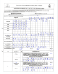
ADDRESS DECODER OPERATION
Refer to the schematics, documents #105119 (7503j·or #105298 (7506)
The 7503 and 7506 use three cascaded 74lS42 decoders (U3, U4 and US) to
decode address lines AO-A7. These decoders are enabled only when 10RQ*,
RD* and 10EXP* are active. The output of the decoder circuit, select
signal SZ*, is active only when the card is addressed to read. This signal
is used to enable the input port, U2.
CHANGING THE PORT ADDRESS OF THE 7503 AND 7506
Refer to the assembly diagrams, documents #105120 (7503) or #105299 (7506)
locate decoders U3, U4 and US (74LS42) adjacent to the STO BUS edge connector.
Each decoder device has a dual row of pads of which form decoder output
select matrices. Make one (and only one) connection to each of the matrices
adjacent to U3, U4, and U5.
The decoder jumper pad numbering figure shows the numbering of the pads
adjacent to the decoder chips on the 7503 and 7506. Also shown are the
jumpers (at X2, YO, and ZO) which produce the hexadeci.mal port address.40,
the selection made when the card is shipped.
()
I
sx
u3
0
•0 , l •s
0
0
0
"
0
0
•
0
•f
0
0
0
0
•
7
U4
Sy
%
0
sz
0
0
,
I
0
0
0
0
"
a
o
0
a aa
0
0
US
X~ o
It
o
I
~
~
o
•
J
. ..
0
0
The I/O address mapping and jumper selection table for one address per card
shows where to place jumper straps to obtain any port address in the hexadecimal range OO-FF. Using the lower of the 2-digit hexadecimal addresses
desired, find the most significant hexadecimal address digit along the
vertical axis, and the least significant hex digit on the horizontal axis.
For example, port address 40 is obtained by connecting jumpers at X2, YO
and ZOo
The I/O Address Mapping and Jumper Selection Table for one address per card
shows where to place jumper stra"ps to obtain any port address in the hexadecimal range OO-FF. Using the lower of the 2-digit hexade~imal addresses
desired, find the most significant hexadecimal address digit along the
vertical axis, and the least significant hex digit on the horizontal axis~
For example, port .address 40 is obtained by connecting jumpers at X2, YO
and ZOo
o
The pad matrices adjacent to U3, u4 and US are on 0.10 inch (0.25cm) centers.
The jumper wires may be conveniently replaced by w·irewrap post if frequent
address selection changes are anticipated.
o
o
CAitO 5.UCT OICOOIIt
0
57
IOU"· 35
7-'~2
A7
51
55
13
15
5'
••
17
l' •
52
.5
l'
"
SO
A
53
51
SX"
()
I/O Address Decoder And Schematic For 1 Address Per Card
MOST
SIGNltrlCANT
HEX ADDRESS
0
• I
ZO
9
I
A
y.
I a 1 C i DIE 1 ,
_z
I Zl I Z2 I Z3 I Z.& I ZS I Z6 I Z7
xo v'
"
1
xo
'1'2
XO
'1'3
2
Xl
'1'0
Xl
'(1
3
Xl
'1'2
Xl
'1'3
4
X2
'1'0
X2
'1'1
5
x2
Y2
x2
'(3
X3
yo
x3
VI
X
X3
'1'2
x3
AND
Y
•
•
7
o
JUMP!R
SELECTION
x.
Z
LEAST SIGNIFICANT HEX ADORISS
0/1/2/3/415/.1'
ZO T Zl r Z2 I z31 z. r zsl Z6 I Zi
xo va
u
yo
X4
Y3
'(1
t
U
X4
'(3
A
"<5
'1'2
yo
X5
VI
•
"(s
'1'2
x6
va
xs
)(6
'(3
C
0
)(6
'(2
x6
'1'3
I
-..7
yo
X7
Y1
F
X7
'(2
-..:
'1'3
VI
/
•
I/O Address Mapping And Jumper Selection Table For 1 Address Per Card
o
7503 AND 7506 ENVIRONMENTAL SPECIFICATIONS
RECOMMENDED OPERATING LIMITS
PARAMETER
Free Air
Humidity
CD
Temp~rature
CD
ABSOLUTE NON-OPERATING LIMITS
MIN
TYP
MAX
MIN
MAX
UNITS
0
25
55
-40
75
°c
95
a
95
%RH
S
Non-condens i n9 re 1at i ve humi d i ty
o
o
ELECTRICAL SPECIFICATIONS FOR THE 7503
()
7503 Optolsolated Input Card Electrical Specifications
RECOMMENDED
OPERATING LIMITS
PARAMETER
MNEM.
ABSOLUTE
NON-OPERATING LIMITS
MIN.
TYP.
MAX.
MIN.
MAX.
UNIT
Vee
Supply voltage
4.75
5.00
5.25
0.0
7.00
Volt
TA
Free air temp.
0
25
55
-40
75
°e
User Electrical Charactertstlcs over Recommended Operating Limits
MNEM.
()
LOW RANGE
PARAMETER
TYP.
MIN.
HIGH RANGE
MAX.
MIN.
TYP.
MAX.
UNIT
V1H
High level user input voltage
4.5
22.0
20.0
130.0
VRMS
VIL
Low level user input voltage
0
3.0
0
3.4
VRMS
IIH
High level user current
0
10.0
.5
2.5
mA
IlL
Low level user input leakage
current
14.0
/lamp
R,O
Isolation resistance
1010
1010
n
VIO
Isolation voltage
500
500
voe
14.0
STD BUS Electrical Charactertstlcs over Recommended Operating Limits
LOW RANGE
MIN.
Icc
HIGH RANGE
PARAMETER
MNEM.
TYP.
MAX.
150
250
STO BUS supply current
MIN.
TYP.
MAX
UNIT
150
250
mA
STO BUS input load
See STD 7503 Edge Connector Pin List
STD BUS output drive
See STD 7503 Edge Connector Pin List
Switching Charactertstlcs over Recommended Operating Limits
MNEM
,
PARAMETER
FROM
BOTH RANGES
TO
TYP.
MIN
o
TpHL
Active-Inactive
TpLH
Inactive-Active
"
TSTAB
Stabilize
"
&
User Interface STDData Bus
__
e_ae
tbaZh
II p, I,
; ,
COMMENTS
MAX.
36msec. 200msec.
See Timing diagram
"
11msec. 50msec.
See Timin~ Diagram
"
50msec. 250m sec. See Timing diagram
447
¥
$ q
1
41 ;
aUA
";;;14."."*_;;*,1
o
ELECTRICAL SPECIFICATIONS FOR THE 7506
7508 Optolsolated Input Card Electrical Specifications
MNEM
RECOMMENDED
OPERATING LIMITS
PARAMETER
ABSOLUTE
NON-OPERATING LIMITS
MIN.
TYP.
MAX.
MIN.
MAX.
UNIT
Vee
Supply"voltage
4.75
5.00
5.25
0.0
7.00
Volt
TA
Free air temp.
0
25
55
-40
75
°e
User Electrical Characteristics oyer Recommended Operating Lim.ts
MNEM
HIGH RANGE
LOW RANGE
PARAMETER
MIN.
TYP.
MAX.
MIN.
150
140
TYP.
MAX.
UNIT
280
VRMS
7.0
VRMS
1.0
mA
14.0
~amp
V 1H
High level user input voltage
VIL
Low level user input voltage
IIH
High level user input current
IlL
Low level user input leakage
current
RIO
Isolation resistance
10'0
10'0
n
Via
Isolation voltage
1500
1500
VDe
70
4.0
2.0
.50
.50
14.0
o
STD BUS Electrical Characteristics oyer Recommended Operating Limits·
HIGH RANGE
LOW RANGE
MNEM
PARAMETER
Icc
STD BUS supply current
MIN.
TYP.
MAX.
150
250
MIN.
TYP.
MAX.
UNIT
150
250
mA
STD BUS input load
See STD 7506 Edge Connector Pin List
STD BUS output drive
See STD 7506 Edge Connector Pin List
Switching Characteristics over Recommended Operating Limits
MNEM
PARAMETER
FROM
TpHL
Active-Inactive
TpLH
Inactive-Active
"
TSTAB
Stabilize
"
,-
TO
User Interface STDDataBus
BOTH RANGES
MIN
TYP.
COMMENTS
MAX.
36msec. 200msec.
See Timing diagram
"
11msec. 60msec.
See Timing Diagram
"
50msec. 250msec. See Timing diagram
o
o
USER INPUT VOLTAGE
I
v-
I
I
I
~~
I
_I
I
_I
--~:--~i
STD OUTPUT STATE
I
I
I
I TpLH I
I
TpHL
I
I
I
I
I
I
y-
_I
I
I
I
TpLH
-
I
I
I
I
~
TpHL
I
SUPPLY VOLTAGE
STD OUTPUT STATE
5Y~_ _ _ _...-f:1
Oy
__.....,.__~I
~~I__~_______________Y_A_U_D_O_~
_____
ST_A_Tl
_____________________________
I~
I
TSTAa
INPUT ClRCUlT TIMING DIAGRAM
o
o
&CllUMWU£44?iAUgMWM UAiQ:CM.
an
o
INPUT LEOS
.
....!...
ptH II"
----+
ADD.....
r
I
I
2.t3O·
I
If
SV
~=
(
7503 COMPONENT PLACEMENT DIAGRAM
o
INPUT LEOS
....!.
.!..
PIN 1/A _____
ADDRESS
INPUT CONNECTOR
If
Sl
-- .
~
-
- ... -o
KEY BETWEEN
PINS 2/8 AND 31C
0
If
SY
If
7506 COMPONENT PLACEMENT DIAGRAM
o
INTlA'ACE CONNECTOR
PIN UST
PIN NUMBIR
SIGNAL
1IA
AC INPUT 7A
2/B
78
lIC
AC INPUT6A
410
68
SJI
IIF
11M
AC INPUT SA
58
AC INPUT 4A
IIJ
48
tlK
AC INPUT 3A
lOlL
38
111M
AC INPUT 2A
l2/N
28
131P
ACINPUT1A
l~
18
15/S
AC INPUT OA
OB
lIlT
11/U
SPARE
111V
SPARE
7503/7506 InterfKe Connector Pin List
eoal CO.....CTOR ..... US'T
IItNNU......
OUTPUT (LSTTL D..IW)
INPUT (LSTTL LOADS)
.....MONIC
·5 VOLTS
GROUND
-5V
07
08
05
0'""" (LSTTL D..lva)
INPUT (UTTI. LOADS)
MNIMONIC
vce
,
2
GNO
t'f.5
s.>;
.IiS
5.-;
A15
A14
A13
A12
All
A10
20
22
2'
28
23
25
8
10
12
,.
US
18
A'
A.
RO°
MEMRO·
MEMEX· .
MCSVNCO
1
3
5
28
27
30
29
31
32
34
31
31
STATUS 0°
auSAQo
vce ·5 VOLTS
1
GND GROUND
-5V
1 .5:'$
03
02
9 .:;"'i
11 ~
01
13 ~.;
00
15
1
A1
17
1
A8
1
19
A5
A4
21
1
5
a.
1
1
1
1
1
1
33
35
REFAESH"
.. .,.,
STATUS 1°
8USAKo
INTAKo
31
'2
43
.es
48
50
PCI
IN
AUXGND
AUX-V
A3
A2
A1
AO
WRlORa·
IOEXpo
31
40
INTAO°
NMIAO"
PBAESET"
CNTAL·
o
PlNNU......
52
54
45
"51
OUT
53
51 55
-0 ......... ActIIe '-- LReI LotIC
WAITAO°
SVSAEserCLOCK"
PCO
AUXGNO
AUX "V
7503/7506 Edge Connector Pin List
mUM;G.4@,i4i4A ;,
tli;:"
;
(,
;
ij
4#4#$
p
$.
ijMif.NI4AJ; I I .
_".4. ;: '" "
1# Qih4iii,,\i
"' -
, ,'(1;( AMi_4¥' ..
MECHAN I CALI
Refer to the Component Placement Diagram for component placement information.
o
The 7503/7506 meets all sro BUS general mechanical specifications. The
7503/7506 requires clearances of 0.150" on the circuit side and 0.600" on
the component side of the printed circuit board when placed in a Series 7000
card rack.
Clear plastic shields are provided on both sides of the assembly for protection
from high voltage. Both adjacent slots must be vacant for clearance of the
shields and the input connector.
The user can connect the 7503/7506 by using a PC board edge connector with
solder tail connections. The recommended card edge connector is supplied
with Pro-Log assembly ,s18. Also included are a protective hood, all hardware, and keys. The keys must be installed in the position shown in the
component placement diagram.
o
o
--------------
4t)
7503 AND '7506 OPERATING SUBROUTINE MODULE
This section provides a flow' diagram and subroutine to operate your 7503/7506
card. It may be used intact, or used as a model to construct sub.routines
for a specific application. The subroutine is written in BOBO-family assembly
code and will execute on BOBO, BOBS, and ZSO processors. The memory addresses
selected are compatible with Pro-Log's 7S01 (SOB5A) and 7803 (ZSO) processor
cards. The 7503/7506 port addresses used are the address jumper selections
made when the 7503/7506 is shipped.
To use the subroutine in systems other than those described above, the
memory and/or I/O port addresses may require change for compatibility,
The flow diagram presented can be easily translated into the assembly code
used by any microprocessor since they show the steps required to acheive
7503/7506 operation without reference to particular mfcroprocessor.
The following subroutine will compare the present port status with the port
status from the last time that the port was read. To use the routine the HL
pointer must point to a place in memory where port status is stored. Also,
the port must be read into the accumulator before calling the routine. Upon
return from the routine the location that the HL pointer was previously set
will contain new port status. Plus the next four locations will contain
change status.
c
Uses Registers A,
M
M+
M+
M+
M+
1
2
3
4
C, Hand L
XX New Data
XX Old Data
XX Changes
XX Bits to Zero
XX Bits to One
~ Location
HL was set to
Memory after Return
o
==-=-,e._A'.'. "*
. MAl.
"4#7
$#
Q ••W;
$. #.
Mk4JMWiMiWMiMM:WCi4iMMK"iQ44i&WijM,;iA ,.
,,"I
""'¥FA
o
SAV~
B &C
LOAD B WITH
OLD DATA
EXCLUS IVE '''OR''
OLD DATA WITH
NEW DATE
STORE BITS
jTHAT CHANGED
!
o
llANO" OLD DATA
WITH CHANGES
.~
STORE BITS THAT
TO ZERO
~ENT
~
llANO" OLD DATA*
WITH CHANGES
!
STORE BITS THAT
WEHT TO ONE
~.
RESTORE 8 & C
J,
RETURN
o
......
.t....
HEXADECIMAL
G
PA'6
~~~ INSTR.
i
MNEMONIC
LABEL
-
INSTR.
lDPr
lit
-
XX
2
-
)(~
3
I'PA
4
5
-
6
7
8
'''(~Q''~)
psp
4b
77
23
10
A
AS
8
23
C 77
D 4F
E
18
FA'
o '2."3
8
_.>...
•.fAt., ..... J-e·
ti1l)
"::'.S+Dr~ Ol.D n~~" IA ~lC.! Lot.~..\-~o...
sr8N
(<<l)
.,
2~
'c P
•
77
1
GI
cc}
tJ~vl D--~4
°
.-
~TA..1
PLP
RT.S
B
_ _...L....-......;F~ __ ._..._____
_
C
HL
(tU•.)
_
•.._--
I NEW
0.0. "OlD C HAN<::.E,S _
-0 I 0 I
.01.2
t>L 0
_
C HA~6[S
11&61
lOLl) [}ATA
J
+0
-0·····
_
010
00001010 Ba-, ~~
..
'
~ OLD.CJtAtJGES: t;f~
Ot-JE..
"'C.L-. B,~.s. ~ o»~ ; ~ llt.ct Locod-,f) ~
rn Q ,
0,0'
0000' ,.,
•
B · ; ' i:GhIIDr ....
C.
HL
<i)
+- OLD. CHA~l.t>~S: 8;~s ~Q ~ero _
~ Stofe R;ts .f.o ~,.rft .. ~ lJtl(t ~"";4t.n
1
oc. D
Onn" 1 U J
of- OL()
. .0_.
esc.
.. w're
C.,.4,,.c,
UN
+e,~~~",
.t;.OMU'f'ftU.\\"_
'"ELD
III, 00£'0
• (Jlo' I Cd D
I
_
(') .0' '0 QCI 0
c. t\ At-1GE S
a-ts -10 Q~E I
-
D.f i'~ a~~,-
!
lJ SE~ 2e~*
~AM MEMOUV'
AfrEl< ~e.~UT ~
l(useS 5 1-..J.:"k"\
...
~
E
-
B
I c.. p
5
o
Be
'
..~~u",."~,,
+- S-loff'
4
c
XX
(l-\l)
(MI\
A~A
A
B
. ;'Tnp~ y~w ~""'Q.
f+) tJtW ~ CH~tJGES
,( P
HL
":,54cJte (H·"v-·~ '''' ...)(-4-- lftt_a4'611\
C; "'A~ ( I l l ) .
LO C A ·
.- Pv4 CWt.,~. i", C
Lo A
8
... ~t- O&-.() ~T" UJ A
77
8
"~~rl1>t)ik-\-\~r
STAN
'IF
AI
•
DATE
+- Pvf OLD ~~CIIr ;If\
X RA
_
,COMMENTS
M l~l)
76
3
'15D'3/'15oio
l.DB
ANA
\( P
~rA~
LI)A
1
2
TITLE
MODifiER
o
1
CS
-
..~
A
9.: "'.I.....
HL
- -..
')()( ~eWM"A I M
XX
DLD DI\TA
~
Ct\A~6£S
.
"-)(_i~ts
X~
,.f+ I
. M-t2.
+b .~em
M+l
S;tS"h!DU£ M+'-I.
'"
o
o
o
SIGNAL
CONVEeSION
.;-n-A>I~U<
CIRCiJIT5
+E>V
CR9-1
'LD-4b4
ID7l1i
£:ARO SELECT DECODERS
r---@
INPUT PORT
107*
bt
U2
D7
'4LC,,40 ~--@ 06
Li:.
7
(j2)
f)')
ACiOC
INTERFACE
CONNECTOR
A4 (21~
141
A:1 (?:>~
I~
IA
Li:.
I
A? (?5~
I~
AI. (27~
141
A() (?~~
I~I
Li:.
~SZ"
I-'CO~,
PC.I~
-5V
I!.\
®----<>
-5V@---o
+~V~
+5V
GND
~2
:>,
GND 4
1ll[l~!1;,!?!,
I I·
DPTOISOLATOR CIRCUIT 0
Iv
NOTFS UNl ESC ()1H[HWI',[ ',PEW 1m.
T5V
CJ: o,13
+IT'~I'F
SOV
50V
f---+----4.----.
~)X "lflt(,TC\ I OFr'I ~{Or.K(),·J,:II'OI<r~i PI:.H P,I()r:K.
Sy ~'IFL[LT'>1 I()F4 kIOCK~),eH)j{f', I'LR R!()!~K..
c.,7 ,',flEeT", 10F B I'Dln Af)/)I~f:',',f',-
PRO-LOG CORPORATION
N/C
@Z!)f------~SPAR[
~~
ASSEMBLY
105120
PARTS LIST 105121
8
5
6
7
4
3
2
.'VIIIONI
_,,,",,,,
A
B
REVI,)E!'i PER PCN 0')',2
R[VI~ED PER PC~ ,14C
~
DI
ID
~
~REF
f'"
,--{37) 2 REDD
~!>if O£TAIL B
,--{ 5)
,,34) 8 REaD
,--{48)
(3~
~
IOO!:iJ
~
6
ImQJ
c::::::
CI
IC4 II~
U2
m
0
R12
"111·1~61~~
6
~
6
Bl!l~
II \I
III
IC
~6
6
IOOlQI
m
,
6
RI6
.
6
lOOil
IOOEiI
~''''"
~6
6
~
~
6
6
,
W~D
BI
~~
,6HI"
~
2
IRI
~
,
~
,
@~
1122
0
1124
,
~.
0
4 R(GJl)
&@-/
35)
IB
IIII
4f(£QD
B R£QD
&
&
1{(iN !)X F;1().1:.I4,lb 18 20,22,'-4
L23 2.21\ CF
'/~
IIJ
-.1.
R~,II,I' .1~.IJ.19,21.C'
47()i\ N[[!f.M(t
21 IOKeF 114VV, 5,),.
r~~~<'f
17 MDA92t»'-7
5RI-<',
RI-8
lib
15
14
13
12
IN4148
CRI·
LD464
CR9,IO
II
10uF ~'''V
I"F 50V
(4
.I,..F 50V
.01", 50v
CI,3,IO,I'
(14 2'
10
7. REF D£~IGNATION,) ARE FOR LOCATING PURR:)SES ONLY
AND MAY NOT APPEAR ON ACTUAL PART.
AI
[24- :?'3~~CCF
In
~
,;:r'lll
9
S
IDE.NTlfY rvlTH ASSY REV LETTE.R USING RUBBER STAMP.
7
INOICArE.5 CATHODE PIN OF LED (TYp)
ITEM DESCRIPTION
REF. DESIGNATION
PRO-LOG CORPORATION
&MAPPED TO PORT 40.
&APPLY LOCKTITE. TO SCREWS.
Lt
SCHEMATIC
PARTS LIST
DE.NOTES PIN I £ND OF ICO,I. BOARD TO WNFORM WITH AS~E.MBLY STANDARD ASIOO4.
NOT[5: UNLESS OTHERWISE SPE.Clf 1[0.
1!JI:l~~
o
8
7
6
5
4
o
3
105119
10!)121
10
2
o
JA
,
•
•
-
aUII.O ••
S',c~~.
~OUllfXSIO·'
!::"':lJ,T5
+SY
t5V
•
:~
6 ~i'; 6
I..OL
11.7
h COOi
..
fA
CI
r.R4-
g~0A~7_ _ _ _
.r
A4
I - - - - - - • !IV
,---,
tf
tt!»' t
~8J
~
~-I
lo,.f I
." 25V
I
~----.~
,
t
,~
~
+'!iV
~
Rl5~2
.,OA
"
~
17
8
on-A
lO·A~
WDC
""(RfAC[
toNNttTOR
L
A3 (23~
~a
L-~~
.. (,7
14LS20t4
I ,,I>1tl39
'
... 1."~M-7
0PT0ISdA100 CIRCUIT ..
1l __ ~_
~ 05
11>-:
@04
0
®
(lYPl
16
II
9
03
02
"
I
IA
A2
AI
IA
';'1
/ItO (29)
REFERENCE ONL'
5Z-
IICO@)---,
pt.'(§}---J
-5Y
l'i'\
SK'5HEeTS • or 8 et.OC"'~" 32 f'(}qT5 pm Blnc.....
5Y.~EL[CT& lor. Bl.OCI'.!>.8 ronr:-. P['~ RlOCI<..
SZ.S[l[CT5 lor 8 POIlT AOORf.sc;r5.
NOTES: UNl[5S OTH£RWIS[ 5f'EC'fI[O.
<D--
-!IV@--
.!»y~
UY 2
::~
r-r·
+ .~~
p
OPTOI~ATOR
5V
1q.~.1O.13
I~~rJ~r
CIRwn 0
PRO-lOG CORPORATION
CPIO·4
LD'4f·.,s
"'6/
HIe
'00«
~SPAR[
_==---;;:;;;-;:-..;:;;;:-r----.-_..- ..- . -
A5SEMBlY
10" z~,
rlllHS LIST 10 S
~~
J(It!
~:~~:!t~~
,-",..
"_IC
•
•
o
u..
o
o
~
23
o
o
o
8
7
6
5
4
3
2
-
1
.........
A.
KI VhL Ll peR POI," Jo'BI·'·"·I"'_
~
DI
ID
~
r-C)<i'
~."
~
SEE Cl TAli..... £3
DETAIL A
CI
~"J~
~
6
~
&U!:il
I~m
r
®-~
"-
111 V
//r-B
Iii
Ie
1111
IB
0
~6
o
~"5
~
~
~"6~
~
~
~
BI
1#1
~~
~
,IIIIDf
2 ...
~
o
R:fi!:iI
@~
6
I
HII.H
l,oLI--I
'~~~~REo.l.l
~
•
0
124
.
r24
'~:J'fTT/2w---5% 'R1O.12.14.16.18.20.22.24
23 KJJ~ CFI/2W !}')'. R~.II.I.~.I!}J1.~.21.23
22 470Jl NCT/lJOl:k R2!}'i'6
21 IOKCF 1/4W !}% RI-8
~
0
17 M0A92Q!\-7
SRI C !>~72
I~
@-/
(A@---J
81?E6J.
AI
& ICltNTlFV WI1 H A"~EMI:.LI R[V.
LEITER USING RUBBER STAMP.
I£::. INDICATES CATHODE PIN OF LED
15
14
13
12
II
RI:.Cl
10
8
7
IOuF ~"W
I"F 50V
(2.5-911.12
C4
.I.. F sov
.OI..F 50v
CI.3.10.13
04-21
~+5b.:U
Cklt)
REF. DESIGNATION
PRO- LOG CORPORATION
&
INDICATE!> PIN NO. I OF SOCKETS <TYPl.
I. fOR ASSV PROCEDURES SEE ASIOO4.
NOTES: UNLE.55 OTHERWISE SPECIfiED.
I
CR~
ITEM DESCRIPTION
&APPLY LOCJ<TITE. TO SCREWS.
8
CR."
L04b4
9
(TIP)
&MAPPED TO PORT 40.
-1