1
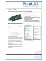
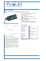
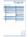
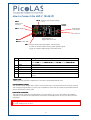
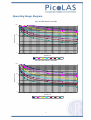
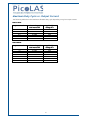
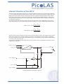
User Manual Rev. 1109 1109 LDP-V 10-70 LDP-V 40-70 Before powering on your unit, read this manual thoroughly and make sure your understood it fully. Please pay attention to all safety warnings. If you have any doubt or suggestion, please do not hesitate hesitate to contact us! Schulz-Electronic GmbH Dr.-Rudolf-Eberle-Straße 2 D-76534 Baden-Baden Fon +49.7223.9636.30 Fax +49.7223. 9636.90 [email protected] www.schulz-electronic.de Table of Contents LDP-V 10-70 Data Sheet ............................................................................................................. 3 LDP- V 40-70 Data Sheet ............................................................................................................ 4 How to Get Started .................................................................................................................... 5 How to connect the LDP-V 10/40-70 .......................................................................................... 6 Operating Range Diagram .......................................................................................................... 7 Maximum Duty Cycle vs. Output Current.................................................................................... 8 Internal Structure of the LDP-V ................................................................................................... 9 How to Use the Internal HV-DC-Supply..................................................................................... 10 Pulse Output............................................................................................................................. 10 Trigger Input............................................................................................................................. 11 Absolute Maximum Ratings ...................................................................................................... 11 2 LDP-V 10-70 Rev. 09.01 valid from April 2009 LDP-V 10-70 Ultra-compact Driver Module for Pulsed Lasers Ultra-compact OEM-module: 32x15mm 2.5 to 13 A output current < 4 ns rise time Pulse width control via trigger input (15 ns to 1 µs) Rep. rates from single shot to 100 kHz Single +15 V supply Current monitor Applications: LIDAR, Measurements, Ignition, Rangefinding, Biochemistry, ... Technical Data:* Output current Max. output voltage - int. High voltage: Rise time Trigger delay Min. pulse duration Max. pulse duration Trigger range Max. Duty factor Trigger input Current monitor Supply voltage Max. Power Dissipation Dimensions Weight Operating temperature Figure: Current monitor output, scale: -2 A/Div Product Description: The LDP-V 10-70 is the smallest availiable source for nanosecond pulses. The device is optimized for size and functionallity, integrating a HV-DC source and the pulsing stage into only 4.8 cm². Its typical application is driving pulsed laser diodes. Those can be mounted directly onto the LDP-V, eliminating the need for strip lines. The diode must be electrically isolated from earth (chassis) ground. Despite its small size, the LDP-V is designed for ease of use. It eliminates the need for multiple peripheral supply units. A single 15 V DC-supply and a triggering signal are all which is required for operation. 2.5 .. 13 A 70 V 15 .. 70 V, 0.1 A, 3 W typ. 3 ns, max. 4 ns typ. 36 ns, max. 40 ns 10 ns 1 µs single-shot to 100 kHz** (refer to diagram with operating limits) 0.1 % 5 V into 50 Ω via SMC-jack 2 A / V into 50 Ω + 15 V 0.2 A 2W 32 x 15 x 8 mm 4g -20 to + 55 ° C * Measured into a short instead of laser diode. Technical data is subject to change without further notice. ** See manual for detailed information. 3 LDP- V 40-70 Rev. 09.01 valid from April 2009 LDP-V 40-70 Ultra-compact Driver Module for Pulsed Lasers Ultra-compact OEM-module: 32x15mm 8 to 40 A output current < 7 ns rise time Pulse width control via trigger input (15 ns to 1 µs) Rep. rates from single shot to 100 kHz Single +15 V supply Current monitor Applications: LIDAR, Measurements, Ignition, Rangefinding, Biochemistry, ... Technical Data:* Output current Max. output voltage - int. High voltage: Rise time Trigger delay Min. pulse duration Max. pulse duration Trigger range Current monitor output, scale: -10 A/Div Product Description: The LDP-V 40-70 is the smallest availiable source for nanosecond pulses. The device is optimized for size and functionallity, integrating a HV-DC source and the pulsing stage into only 4.8 cm². Its typical application is driving pulsed laser diodes. Those can be mounted directly onto the LDP-V, eliminating the need for strip lines. The diode must be electrically isolated from earth (chassis) ground. Despite its small size, the LDP-V is designed for ease of use. It eliminates the need for multiple peripheral supply units. A single 15 V DC-supply and a triggering signal are all which is required for operation. Max. Duty factor Trigger input Current monitor Supply voltage Max. Power Dissipation Dimensions Weight Operating temperature 8 .. 40 A 70 V 15 .. 70 V, 0.1 A, 3 W typ. 6 ns, max. 7 ns typ. 36 ns, max. 40 ns 15 ns 1 µs single-shot to 100 kHz** (refer to diagram with operating limits) 0.1 % 5 V into 50 Ω via SMC-jack 20 A / V into 50 Ω + 15 V 0.2 A 2W 32 x 15 x 8 mm 4g -20 to + 55 ° C * Measured into a short instead of laser diode. Technical data is subject to change without further notice. ** See manual for detailed information. 4 How to get started Step # What to do Check 1 Unpack your Device 2 Make a short at the output 3 Turn the High voltage to the lowest value (turn potentiometer fully counterclockwise) 4 Connect a Pulse source with the desired pulsewidth to the triggering Input 5 Connect your oscilloscope to the current monitor output. Pin 1 for signal and Pin 2 for ground. Select 50 Ohm termination, trigger on negative falling edge, scale 200 mV/div. 6 Apply the supply voltage Security Advice Advice: Do not touch any leads of the output or the output capacitors as they are connected to a high voltage of up to 70 V. Connect a 15 V DC power supply to the pin-header. See page 5 for details. Note: Note Some power supplies show a voltage overshoot during turn on/turn off. This may damage the driver. Please Clamp input to output or sold a wire. e.g. 100 ns, 100 Hz repetition rate. make sure that your supply does not have any voltage surges when powered on or off. 7 Adjust the value of the desired pulse current. Turn the potentiometer clockwise until the current reaches the desired level. 8 Disconnect the supply, remove the short at the output and connect the laser diode 9 Reconnect the supply and check the optical output of your laser diode. 5 Pay attention to correct polarity. Anode (+1): top, Cathode (-): bottom Note: The actual current is always some percent lower than the value adjusted in step 7. Fine-adjust the current now by means of turning the potentiometer. How to Connect the LDP-V 10/40-70 Pin 5: 5 connect input supply voltage + 15 V Pin 6: 6: External HV setpoint Output + 15 V Pin 3: 3 Trigger in Laser-DiodeConnection Anode (+) Potentiometer to adjust value of HV-DC Pin 2: 2: Pin 4: Ground GND Pin 1: connect oscilloscope (impedance: 50 Ohm) here In order to monitor diode current, yields negative signal trigger on negative falling edge, scale 200 mV/div Pin Name Description 1 I_mon 2 GND Current monitor output into oscilloscope 50 Ohm; negative signal Scale: 2 A/V for the LDPLDP-V 1010-70 and 20 A/V for the LDPLDP-V 4040-70 Ground return 3 Trigger_In Trigger Input: 5 V into 50 Ohm 4 GND Ground return 5 +15V Supply Voltage, connect to a power supply: + 15 V DV 6 U_HV_Ctrl External HV setpoint input; allows control over the internal HV-DC source. Trigger Input: The trigger input requires a signal level of 5 V and is terminated with 50 Ohm. Current Monitor Output: The current monitor output has a scale of 2 A/V for the LDP-V 10-70 and 20 A/V for the LDP-V 40-70 with a negative signal output. It has a source impedance of 50 Ohm and must be terminated with 50 Ohm to achieve the correct scale. Laser Diode Connection: The Laser Diode connection is designed for a 3-pin housing (e.g. TO-52). The Pad for the cathode connection is located on the bottom side of the driver; the anode pad is on top. The third pad is not connected. Security Advic Advice: Do not touch any leads of the output or the output capacitors as they are connected to a high voltage of up to 75 V. 6 Operating Range Diagram LDP-V 10-70: Max. Reprate vs. Pulsewidth Repetition rate in kHz 100,0 10,0 1,0 0,1 0 100 200 300 400 500 600 700 800 900 1000 800 900 1000 Pulsewidth in ns 2,5 A 3A 4A 6A 8A 10 A 13 A LDP-V 40-70: Max. Reprate vs. Pulsewidth Repetition rate in kHz 100,0 10,0 1,0 0,1 0 100 200 300 400 500 600 700 Pulsewidth in ns 8A 10 A 15 A 20 A 7 25 A 30 A 40 A Maximum Duty Cycle vs. Output Current The following tables show the maximum allowable duty cycle depending on a given output current. LDPLDP-V 1010-70: 70: Output current in A 2.5 3.0 4,0 6.0 8.0 10.0 Maximum Maximum duty cycle with internal internal HV 0.0320 0.0222 0.0125 0.0056 0.0031 0.0020 Typical High Voltage in V 18.5 21.5 27.5 39.6 51.6 63.6 Maximum Maximum duty cycle with internal internal HV 0.0098 0.0063 0.0028 0.0016 0.0010 0.0007 0.0004 Typical High Voltage in V 17.2 20.6 29.2 37.7 46-3 54.8 71.9 LDPLDP-V 4040-70: 70: Output current in A 8 10 15 20 25 30 40 8 Internal Structure of the LDP-V The LDP-V series generates the pulses by a simple but efficient principle. First, the storage capacitors (CS) are charged through the internal HV-DC-supply. When a pulse is applied at the trigger input, the high speed mosfet opens and the current flows from the capacitor through the laser diode, mosfet and current sense resistors. At the end of the pulse, the mosfet closes again and the current stops. The generated current depends on the applied high voltage, the laser diode compliance voltage and its differential resistance. The following formulas give a good estimation of the laser diode current depending on the driver’s high voltage supply UHV, the laser diode compliance voltage Ucomp and its differential resistance Rdiff: LDP-V 10-70: I LD ≈ LDP-V 40-70: I LD ≈ U HV − Ucomp 6 + Rdiff U HV − Ucomp 1.7 + Rdiff The laser diode current is measured with current sensing resistors (I_Mon). The trigger-input provides full control of the driver’s pulsing capability to the user. The required DC high-voltage is generated with the integrated HV-DC-supply. The internal supply is controlled by the HV setpoint potentiometer or via the U_HV_Ctrl (Pin 6) pin. The Diode DRP prevents the laser diode from reverse currents. An over temperature protection is NOT integrated on the driver. Pin 6: U_HV_Ctrl 15 V ++++ Pin 5: +15 V 18 .. 70 V LD DRP ---CS Pin 3: Trigger_In Driver 50 R 50 R Pin 1: I_Mon RCS Pin 2, 4: GND Internal Structure of the LDP-V 10/40-70 9 RCL How to Use the Internal HV-DC-Supply The LDP-V series provides an internal high voltage supply (up to 2.5 W / 0.1 A / 70 V). To adjust the laser diode current to the desired value follow the steps below: 1. Turn the potentiometer fully counterclockwise 2. Apply the 15 V supply voltage 3. Start pulses 4. Measure the diode current 5. Adjust the level of the high voltage supply (hence the level of the current) by turning the potentiometer clockwise The HV-DC-Supply can also be controlled through an external setpoint signal on pin 6 of the pinheader (U_HV_Ctrl): A Signal level of 0 V equals the high voltage which is currently adjusted by the internal potentiometer, a signal level of 10 V equals the minimum high voltage. Security Advice Advice: Do not touch any leads of the output or the output capacitors as they are connected to a high voltage of up to 75 V. Pulse Output The LDP-V series provides ultra rapid pulse rise- and fall-times in the region of several nanoseconds. However, pulse rise and fall depend on the parasitic stray inductance of the cabling towards the laser diode. Direct connection without any kind of wires to the module is absolutely necessary for best results. For detailed information about the effect of the laser diode connection on the pulse shape please refer to PicoLAS Application Notes #2 and #3. Typical Pulse Rise and Fall Times (scale: 10 A/Div) 10 Trigger Input The trigger input on the pin header (Pin 3) is terminated with 50 Ohm to ground. The trigger source has to be able to provide a signal level of 5 V with a 50 Ohm load. The delay between the triggering signal and the load-current is very low around 36 ns and very constant. The pulse-to-pulse jitter is very stable below 1 ns if supply voltage and temperature are kept constant. Typical trigger delay of LDP-V 10/40-70 Absolute Maximum Ratings Supply voltage range: 12 .. 18 V Max. voltage at HV Pin: 75 V Input voltage range U_HV_Ctrl: 0 .. 10 V Input voltage range trigger input: 0 .. 10 V Security Advice Advice: Do not touch any leads of the output or the output capacitors as they are connected to a high voltage of up to 75 V. 11