1
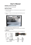
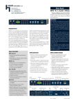
User Manual Rev. 14.04 LDP-V 03-100 UF3 PicoLAS GmbH Company for Innovative Power Electronics and Laser Technology Kaiserstrasse 100 52134 Herzogenrath Distribution: Table of Contents LDP-V 03-100 UF3..............................................................................................................................3 How to connect the LDP-V 03-100 UF3...............................................................................................5 Operating Range Diagram ................................................................................................................. 7 Maximum Duty Cycle vs. Output Current ...........................................................................................9 Current Droop vs. Pulse Duration .......................................................................................................9 Internal Structure of the LDP-V........................................................................................................ 10 How to use the Internal HV-DC-Supply ............................................................................................ 11 Pulse Output.................................................................................................................................... 11 Trigger Input .................................................................................................................................... 12 Trigger-Output-Monitor .................................................................................................................. 13 Absolute Maximum Ratings ............................................................................................................. 13 Mechanical Details of the Base-Plate ............................................................................................... 14 2 LDP-V 03-100 UF3 Rev.12.12 LDP-V 03-100 UF3 Driver Module for Pulsed Lasers Compact OEM-module 0.3 to 3A diode current < 1.2 ns rise time Pulse width control via SMC trigger input (1 ns to >10 µs) Rep. rates from single shot to 35 Mhz Single +15 V supply Current monitor and isolated monitor Applications: LIDAR, Measurements, Ignition, Rangefinding, Biochemistry, ... Technical Data:* Output current Max. output voltage - int. high voltage: Rise time Trigger delay Min. pulse duration Max. pulse duration Trigger range Trigger input Trigger output Figure: Current monitor output, scale: -0.4 A/Div Product Description: The LDP-V 03-100 UF3 is a small and inexpensive source for nanosecond pulses. The device is optimized for pulse-repetition from single-shot up to MHz-repetition with duty-cycles up to 100% * * . Its typical application is driving pulsed laser diodes. Those can be mounted directly onto the LDP-V, eliminating the need for strip lines. The diode must be electrically isolated from earth (chassis) ground. Compatible packages: TO-18, TO-5, TO-52, 5.6 mm, 9 mm and similar. Despite its small size, the LDP-V is designed for ease of use. It eliminates the need for multiple peripheral supply units. A single 15 V DC-supply and a triggering signal are all what is required for operation. Additionally, the LDP-V can be extended with the PLCS-21 controller to enable USB2.0-communication with a PC or the operating unit PLB-21. Current monitor Supply voltage Max. pow er dissipation Dimensions Weight Operating temperature 0.3 .. 3 A (max 3.5 A)* * 100 V 0 .. 100 V, 1 A, 15 W typ. 800 ps, max. 1.2 ns typ. 2.5 ns, max. 4 ns 1 ns > 10 µs* * single-shot to 35 M hz* * (refer to diagram with operating limits) 5 V into 50 Ω via SMC-jack galvanically isolated Rogowski-coil 2.0 A / V into 50 Ω 12 .. 15 V DC, 2.2 A optional: 0 .. 100 V, 15 W (external high voltage) 15 W 75 x 44 x 20 mm 76 g -20 to + 55 ° C * M easured into a short instead of laser diode. Technical data is subject to change w ithout further notice. * * See manual for detailed information. PicoLAS strongly recommends the use of the PLCS-21 to achieve best results. Optional Accessories: PLCS-21 PLB-21 LDP-V-BOB LDP-V-KIT 3 How to get started Step # What to do Check 1 Unpack your Device 2 Make a short at the output 3 Turn the High voltage to the lowest value (turn poti fully counterclockwise) 4 Connect a Pulse source with the desired pulsewidth to the selected triggering Input 5 Connect your Scope Select 50 Ohm termination, trig on neg. falling edge, 200 mV/div. 6 Apply the supply voltage Connect a 15 V DC power supply to the pinheader. See page 5 for details. Security Advise: Do not touch any leads of the output or the output capacitors as they are connected to a high voltage of up to 100 V. 7 Adjust the value of the desired pulse current. (turn the poti clockwise until the current reaches the desired level.) 8 Disconnect the supply, remove the short at the output and assemble the Laser Diode (Polarity!) 9 Reconnect the Supply and check the optical output of your Laser Diode. e.g. 100 ns, 100 Hz reprate. Note: Some supplies have a voltage overshoot during turn on/turn off. This may damage the device. Note: The actual current is always some percent lower than the value of step 7. Adjust the current with help of the poti. 4 How to connect the LDP-V 03-100 UF3 Rogowski-Coil Solder-junction to activate the internal HV-supply Poti to adjust value of HV-DC Laser-DiodeConnection Pin 10 Pinheader Pin 2 Trigger-Input SMC Current-monitor-output into 50 Ohm Connections via Pinheader: Pin Name Description 1 GND Ground return 2 HV+ External high-voltage supply Input (0 .. 100 V) for connecting an alternative HV-DC supply. See page 9 for details. 3 GND Ground return 4 +15 V Supply Voltage, connect to a power supply. 5* Disable_Poti Disables the internal HV-setpoint poti when set high. 6 Pulse_In Trigger Input into 50 Ohm 7 Disable Not connected. 8* U-Monitor High-volage monitor output (scale: 40 mV/V) for supervising the actual high voltage. 9 NTC Internal 10 kOhm NTC versus GND for temperature monitoring. (B-value: 3620) 10* Ext_HV_Setpoint External HV setpoint input (scale: 25 V/V) allows control over the internal HV-DC source. *These pins had to be left unconnected in older versions then V3 Trigger Input: The trigger input requires a signal level of 5 V and is terminated with 50 Ohm. Current Monitor Output: The current monitor output has a scale of 2 A/V with a negative signal output. It has a source impedance of 50 Ohm and must be terminated with 50 Ohm to achieve the correct scale. Laser Diode Connection: The Laser Diode can either be connected via the mounting holes on the top side of the pulser (inner hole: Anode, outer hole: Cathode) or at the rectangular pads on top (Anode) and bottom (Cathode) of the pulser. Security Advise: 5 Do not touch any leads of the output or the output capacitors as they are connected to a high voltage of up to 100 V. 6 Operating Range Diagram LDP-V 03-100 UF3: Max. Reprate vs. Pulsewidth (internal HV, with cooling) 10.000 Repetition rate in kHz 1.000 100 10 1 0 100 200 300 400 500 600 700 800 900 1000 900 1000 Pulsewidth in ns 0,5 A 1,0 A 1,5 A 2,0 A 2,5 A 3,0 A 3,5 A LDP-V 03-100 UF3: Max. Reprate vs. Pulsewidth (internal HV, without cooling) 10.000 Repetition rate in kHz 1.000 100 10 1 0 100 200 300 400 500 600 700 800 Pulsewidth in ns 0,5 A 1,0 A 1,5 A 2,0 A 7 2,5 A 3,0 A 3,5 A LDP-V 03-100 UF3: Max. Reprate vs. Pulsewidth (external HV, with cooling) 10.000 Repetition rate in kHz 1.000 100 10 1 0 100 200 300 400 500 600 700 800 900 1000 900 1000 Pulsewidth in ns 0,5 A 1,0 A 1,5 A 2,0 A 2,5 A 3,0 A 3,5 A LDP-V 03-100 UF3: Max. Reprate vs. Pulsewidth (external HV, without cooling) 10.000 Repetition rate in kHz 1.000 100 10 1 0 100 200 300 400 500 600 700 800 Pulsewidth in ns 0,5 A 1,0 A 1,5 A 2,0 A 8 2,5 A 3,0 A 3,5 A Maximum Duty Cycle vs. Output Current The following tables show the maximum allowable duty cycle depending on a given output current. With active cooling of the baseplate: Output current in Max duty cycle A with ext. HV 0,5 1,00 1,0 0,40 1,5 0,18 2,0 0,10 2,5 0,06 3,0 0,04 3,5 0,03 Typical High Voltage in V 14,3 27,0 39,7 52,4 65,1 77,8 90,5 Max duty cycle with int. HV 1,59 0,40 0,18 0,10 0,06 0,04 0,03 Without cooling of the baseplate: Output current in A Max duty cycle with ext. HV 0,5 0,71 1,0 0,18 1,5 0,08 2,0 0,04 2,5 0,03 3,0 0,02 3,5 0,01 Typical High Voltage in V 14,3 27,0 39,7 52,4 65,1 77,8 90,5 Max duty cycle with int. HV 0,71 0,18 0,08 0,04 0,03 0,02 0,01 Current Droop vs. Pulse Duration The following table shows the absolute output current droop (in A) versus pulse length. Pulse durations shorter than one microsecond are not considered as the droop is typically lower than 1%. Pulse Duration in µs Current in A 1 5 10 0,3 <1% <1% <1% 1,0 <1% <1% 0,012 A 2,0 <1% 0,024 A 0,056 A 3,0 0,024 A 0,054 A 0,088 A Typical performance of the LDP-V The following table shows the typically achieved pulse performance using different pulse sources Signal source Typ. Output risetime ( 0 … 2 A) Typ. Output risetime ( 2 … 3 A) Rectangular Pulse signal ( < 100ps rise time) 900 ps 1,1 ns PLCS-21 with SMC-SMC Trigger cable 900 ps 1,8 ns PLCS-21 on Top of the driver 920 ps 2,7 ns Low performance Signal generators > 5 ns > 5 ns 9 Internal Structure of the LDP-V The LDP-V series generates the pulses by a simple but efficient principle. First, the storage capacitors (CS) are charged, whether through the internal HV-DC-supply or an external high voltage source. When a pulse is applied at the trigger input, the high speed mosfet opens and the current flows from the capacitor through the laser diode, mosfet and current sense resistors. At the end of the pulse, the mosfet closes again and the current stops. The generated current depends on the applied high voltage, the laser diode compliance voltage and its differential resistance. The following formulas give a good estimation of the laser diode current depending on the pulser’s high voltage supply UHV, the laser diode compliance voltage Ucomp and its differential resistance Rdiff: I LD ≈ U HV − U comp 23.6 + Rdiff The laser diode current is measured with current sensing resistors (current monitor output) and with the galvanically isolated rogowski coil. Trigger-input provides full control of the driver’s pulsing capability to the user. The required DC high-voltage can either be applied through an external voltage source or it can be generated with the integrated HV-DC-supply. The internal supply is controlled by the HV setpoint poti or, when the Disable_Poti (Pin 5) pin is set high, via the Ext_HV_setpoint (Pin 10) pin. A voltage monitor (Pin 8) provides feedback of the high dc voltage. The Diode DRP prevents the laser diode from reverse currents; a 10kR NTC provides the possibility to monitor the pulser temperature. An over temperature protection is NOT integrated on the driver. Pin 2: + HV Pin 8: U-Monitor +HV-Adjust-Poti 15 V ++++ Pin 4: +15 V 18 .. 90 V LD Pin 5: Disable Poti DRP ---- Pin 10: Ext. HV setpoint CS Pin 7: Disable Rogowski-Coil Pin 1,3: GND Pin 6: Trigger Trigger SMC Pin 9: NTC RCL Driver 50 R 10K 50 R Current-Monitor RCS Rogowski-Coil 10 How to use the Internal HV-DC-Supply The LDP-V series provides a high power (up to 15 W / 1 A / 100 V) internal high voltage supply. To adjust the laser diode current to the desired value follow the steps below. Notice: Make sure that the solder junction is done to activate the HV-DC-Supply. 1. Turn the poti fully counterclockwise 2. Apply the 15 V supply voltage 3. Start Pulses 4. Measure the diode current 5. Adjust the level of the high voltage supply (hence the level of the current) by turning the poti clockwise Since Version 3 of the LDP-V series, the HV-DC-Supply can also be controlled through an external setpoint signal on pin 10 of the pinheader (Ext_HV_Setpoint); the scale is 25V/V. To enable the external setpoint pin and disable the internal poti, pin 5 (Disable_Poti) of the pinheader has to be set to “high”. Otherwise the internal poti will override the external signal. The high DC voltage can be monitored at pin 8 (UMonitor) with a scale of 40 mV/V. Note: Older versions are not capable of these features and the above mentioned pins have to be left unconnected! Security Advise: Do not touch any leads of the output or the output capacitors as they are connected to a high voltage of up to 100 V. Pulse Output The LDP-V series provides ultra rapid pulse rise- and fall-times in the region of several nanoseconds. However, pulse rise and fall depend on the parasitic stray inductance of the cabling to the laser diode. Direct connection without any kind of wires to the module is absolutely necessary for best results. For detailed information about the effect of the laser diode connection on the pulse shape please refer to PicoLAS Application Notes #2 and #3. Typical Pulse Rise and Fall Times of LDP-V 03-100 UF3 (scale: 1 A/Div) 11 Trigger Input The trigger input, both on the pin header and the SMC-jacket, is terminated with 50 Ohm to ground. The trigger source has to be able to provide a signal level of 5 V with a 50 Ohm load. Tpuls 1 ns .. 10 µs Voltage B C A 4,5 .. 5,2 V 0 .. 0,2 V Time Τr Τj < 200 ps Trigger signal demands Notes: A: Exceeding 0.2 V during pulse pause will cause a non proper turning off and thermal damage. B: If the Trigger-altitude is below 4.5 V the device will not turn on properly and can not carry the full current. Exceeding 5.2 V can damage the power stage and will yield in µs-trailing after turn off. C: To achieve best rise times the rise time of the trigger must be as short as possible. Shortest pulse durations are guaranteed with rise times below 200 ps. There is no “Schmitt-Trigger” inside the LDP-V 03-100 UF3. 12 Trigger-Output-Monitor The Trigger Output signal is generated with an integrated, isolated Rogowski-Coil and provides an ultra fast galvanically isolated signal. The signal shape is proportional to the derivative of the load current. It can be used for a current-response triggering signal and has no delay to the load current. Combined with an integrator it is possible to use this signal for a galvanically isolated current monitor. The isolation barrier is suitable for voltages up to 100 V and prevents unwanted ground loops. Signal of the Rogowski-Coil: "True" load current Positive edge at pulse begin Negative edge at pulse end Absolute Maximum Ratings Supply voltage range: 10 .. 18 V Max. voltage at HV Pin: 100 V Max. output current U-monitor, NTC: 1 mA Input voltage range Disable_Poti, Ext_HV_Setpoint: 0 .. 5 V Input voltage range trigger input, Disable: 0 .. 15 V Security Advise: Do not touch any leads of the output or the output capacitors as they are connected to a high voltage of up to 100 V. 13 Mechanical Details of the Base-Plate All dimensions in millimetres. 14