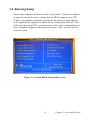
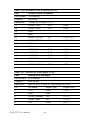
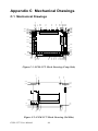
1
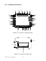
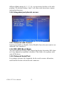
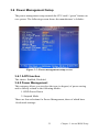
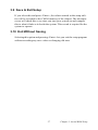
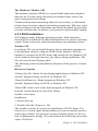
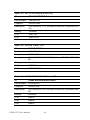
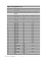
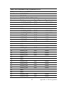
PCM-3372
PC/104+ SBC w/VIA Eden +
CX700, VGA, LCD, LAN, USB2.0
and CF
User Manual
Copyright
This document is copyrighted, © 2006. All rights are reserved. The original manufacturer reserves the right to make improvements to the products
described in this manual at any time without notice.
No part of this manual may be reproduced, copied, translated or transmitted in any form or by any means without the prior written permission of
the original manufacturer. Information provided in this manual is
intended to be accurate and reliable. However, the original manufacturer
assumes no responsibility for its use, nor for any infringements upon the
rights of third parties that may result from such use.
Acknowledgements
Award is a trademark of Award Software International, Inc.
VIA is a trademark of VIA Technologies, Inc.
IBM, PC/AT, PS/2 and VGA are trademarks of International Business
Machines Corporation.
Microsoft Windows® is a registered trademark of Microsoft Corp.
RTL is a trademark of Realtek Semi-Conductor Co., Ltd.
ESS is a trademark of ESS Technology, Inc.
UMC is a trademark of United Microelectronics Corporation.
SMI is a trademark of Silicon Motion, Inc.
Creative is a trademark of Creative Technology LTD.
All other product names or trademarks are properties of their respective
owners.
For more information on this and other Advantech products, please visit
our websites at:
http://www.advantech.com
http://www.advantech.com/eplatform
For technical support and service, please visit our support website at:
http://www.advantech.com/support
This manual is for the PCM-3372.
Part No. 2006337210
1st Edition
Printed in Taiwan
PCM-3372 User Manual
Jun. 2007
ii
Packing List
Before you begin installing your card, please make sure that the following
materials have been shipped:
• 1 x PCM-3372 SBC
• 1 x USB cable w/ 6 ports, 16cm (p/n:1700000897)
• 1 x VGA cable, 15cm (p/n:700000898)
• 1 x PS/2 KB & Mouse cable, 20cm(p/n:1700060202)
• 1 x Serial ATA cable, 100cm (p/n:1700071000)
• 1 x LPT cable, 25cm (p/n:1700260250)
• 1 x Ethernet RJ-45 Conn. conversion cable (p/n:1701100202)
• 1 x COM 1,2 cable, 22cm (p/n:1701200220)
• 1 x IDE cable (p/n:1701440350)
• 1 x RS-422/485 cable, 15cm (p/n:1703040157)
• 1 x MINI-DIN cable, 6cm (p/n: 1703060053)
• 1 x AT power cable (p/n:1703080104)
• 1 x Audio cable (p/n:1703100152)
• 1 x ATX power cable (p/n:1703200380)
• 1 x Startup manual
• 1 x CD-ROM (Manual, Driver, Utility)
If any of these items are missing or damaged, contact your distributor or
sales representative immediately.
Model No. List Description
PCM-3372F-J0A1E
PC/104+ SBC w/VIA Eden 400MHz + CX700,
VGA, LVDS, LAN, Audio, CF, Fanless
PCM-3372F-M0A1E PC/104+ SBC w/VIA Eden 600MHz + CX700,
VGA, LVDS, LAN, Audio, CF, Fanless
PCM-3372F-S0A1E PC/104+ SBC w/VIA Eden ULV 1.0GHz +
CX700, VGA, LVDS, LAN, Audio, CF, Fanless
iii
Additional Information and Assistance
1. Visit the Advantech web site at www.advantech.com where you can
find the latest information about the product.
2. Contact your distributor, sales representative, or Advantech's customer
service center for technical support if you need additional assistance.
Please have the following information ready before you call:
• Product name and serial number
• Description of your peripheral attachments
• Description of your software (operating system, version, application
software, etc.)
• A complete description of the problem
• The exact wording of any error messages
PCM-3372 User Manual
iv
This device complies with the requirements in part
15 of the FCC rules: Operation is subject to the following two conditions:
1.This device may not cause harmful interference,
and
2.This device must accept any interference
received, including interference that may cause
undesired operation
This equipment has been tested and found to comply with the limits for a Class A digital device, pursuant to Part 15 of the FCC Rules. These limits are
designed to provide reasonable protection against
harmful interference when the equipment is operated in a commercial environment. This equipment
generates, uses, and can radiate radio frequency
energy and, if not installed and used in accordance
with the instruction manual, may cause harmful
interference to radio communications. Operation of
this device in a residential area is likely to cause
harmful interference in which case the user will be
required to correct the interference at his/her own
expense. The user is advised that any equipment
changes or modifications not expressly approved
by the party responsible for compliance would void
the compliance to FCC regulations and therefore,
the user's authority to operate the equipment.
Caution!
Achtung!
There is a danger of a new battery exploding if it is
incorrectly installed. Do not attempt to recharge,
force open, or heat the battery. Replace the battery
only with the same or equivalent type recommended by the manufacturer. Discard used batteries according to the manufacturer’s instructions
v
PCM-3372 User Manual
vi
Contents
Chapter
1 Introduction ......................................................2
1.1
1.2
1.3
Introduction ....................................................................... 2
Features ............................................................................. 2
Specifications .................................................................... 3
1.3.1
1.3.2
1.3.3
1.3.4
1.3.5
1.3.6
1.4
Standard PC/104 Biscuit SBC Functions........................ 3
VGA/LVDS Interface ..................................................... 3
Ethernet Interface............................................................ 4
Audio Function ............................................................... 4
OS support ...................................................................... 4
Mechanical and Environmental ...................................... 4
Board Layout: dimensions ................................................ 5
Figure 1.2:Board layout: Dimensions (Solder Side)....... 6
Chapter
2 Installation ........................................................8
2.1
Jumpers.............................................................................. 8
2.2
Connectors......................................................................... 9
2.3
Locating Connectors ....................................................... 10
Table 2.1:Jumper/Switch Setting.................................... 8
Table 2.2:Connector Table ............................................. 9
Figure 2.1:Connectors (component side)...................... 10
Figure 2.2:Connectors (solder side).............................. 10
2.4
2.5
2.6
Setting Jumpers ............................................................... 11
Installing SO-DIMMs ..................................................... 12
IDE, CDROM Hard Drive Connector (CN3).................. 12
2.6.1
Connecting the hard drive............................................. 12
2.7
Solid State Disk............................................................... 13
2.8
2.9
Keyboard and PS/2 Mouse Connector (CN12) ............... 13
Power Connectors (CN20) .............................................. 13
2.7.1
2.9.1
2.9.2
2.10
Compact Flash (CN24) ................................................. 13
Main power connector, +5 V, +12 V (CN38)............... 13
Power Reset button ....................................................... 13
Audio Interfaces (CN25)................................................. 13
2.10.1 Audio connector Audio-out(CN35), Audio-in(CN34) . 13
2.11
COM Port Connector (CN15) ......................................... 14
2.11.1 Serial Port RS-422/485 (CN16).................................... 14
Table 2.3:Serial Port RS-422/485 (J7).......................... 14
2.12
VGA/LCD Interface Connections................................... 14
2.12.1 CRT display connector (CN10) .................................... 14
2.12.2 External LVDS Connector (CN5)................................. 14
2.12.3 External LVDS Connector (CN7)................................. 14
2.13
Ethernet Configuration.................................................... 15
vii
2.13.1 100Base-T connector (CN9)......................................... 15
2.14
2.15
2.16
2.17
Chapter
Watchdog Timer Configuration ...................................... 15
USB Connectors (CN11)................................................. 15
GPIO (General Purpose Input Output) (CN2/CN23)...... 15
SATA Connector (SA1, SA2)......................................... 15
3 Award BIOS Setup.........................................18
3.1
Introduction ..................................................................... 18
3.1.1
CMOS RAM Auto-backup and Restore ....................... 18
3.2
Entering Setup ................................................................. 19
3.3
3.4
Standard CMOS Setup .................................................... 20
Advanced BIOS Features ................................................ 20
Figure 3.1:Award BIOS Setup initial screen ................ 19
3.4.1
3.4.2
3.4.3
3.4.4
3.4.5
3.4.6
3.4.7
3.5
Integrated Peripherals...................................................... 21
3.5.1
3.5.2
3.5.3
3.5.4
3.5.5
3.6
IDE Master/Slave PIO/UDMA Mode,.......................... 21
Integrated peripherals screen ........................................ 22
Onboard LAN Control .................................................. 22
IDE HDD Block Mode ................................................. 22
Onboard Serial Port ...................................................... 22
Power Management Setup............................................... 23
3.6.1
3.6.2
3.6.3
3.6.4
3.6.5
3.6.6
3.6.7
3.6.8
3.6.9
3.6.10
3.7
Figure 3.2:Advanced BIOS features screen.................. 20
Virus Warning............................................................... 20
First/Second/Third/Other Boot Device......................... 21
Boot Up NumLock Status............................................. 21
Typematic Rate Setting................................................. 21
Typematic Rate (Chars/Sec) ......................................... 21
Typematic Delay (msec)............................................... 21
Security Option ............................................................. 21
Figure 3.3:Power management setup screen................. 23
ACPI function ............................................................... 23
Power Management ...................................................... 23
Video Off In Suspend ................................................... 24
Modem Use IRQ........................................................... 24
HDD Power Down........................................................ 24
PowerOn By Modem .................................................... 24
PowerOn By Alarm ...................................................... 24
Primary IDE 0 (1) and Secondary IDE 0 (1) ................ 24
FDD, COM, LPT PORT ............................................... 24
PCI PIRQ [A-D]# ......................................................... 24
PnP/PCI Configurations .................................................. 25
3.7.1
3.7.2
3.7.3
3.7.4
PCM-3372 User Manual
PnP OS Installed ........................................................... 25
Figure 3.4:PnP/PCI configurations screen.................... 25
Reset Configuration Data.............................................. 25
Resources controlled by:............................................... 25
PCI/VGA Palette Snoop ............................................... 25
viii
3.8
3.9
3.10
Chapter
Password Setting ............................................................. 26
Save & Exit Setup ........................................................... 27
Exit Without Saving ........................................................ 27
4 S/W Installation..............................................30
4.1
4.2
4.3
S/W Introduction ............................................................. 30
Driver Installation .......................................................... 30
SUSI Application Library ............................................... 31
4.3.1
4.3.2
4.3.3
4.3.4
4.4
SUSI Introduction ......................................................... 31
SUSI Functions ............................................................. 32
SUSI Installation........................................................... 33
SUSI Sample Programs ................................................ 35
Further Information ......................................................... 36
Appendix A
Pin Assignments ............................................38
A.1
Pin Assignments.............................................................. 38
Table A.1:Jumper Setting ............................................. 38
Appendix B
System Assignments ......................................62
B.1
System I/O Ports.............................................................. 62
B.2
1st MB memory map....................................................... 63
B.3
DMA channel assignments.............................................. 63
B.4
Interrupt assignments ...................................................... 64
Table B.1:System I/O ports .......................................... 62
Table B.2:1st MB memory map ................................... 63
Table B.3:DMA channel assignments .......................... 63
Table B.4:Interrupt assignments ................................... 64
Appendix C Mechanical Drawings.....................................66
C.1
Mechanical Drawings...................................................... 66
Figure C.1:PCM-3372 Mech Drawing (Comp Side).... 66
Figure C.2:PCM-3372 Mech Drawing (Sol Side) ........ 66
ix
PCM-3372 User Manual
x
CHAPTER
1
General Information
This chapter gives background information on the PCM-3372.
Sections include:
• Introduction
• Features
• Specifications
• Board layout and dimensions
Chapter 1 Introduction
1.1 Introduction
The PCM-3372 is a fanless, best-cost, performance PC/104+ SBC (Single
Board Computer) geared to satisfy the needs for various industrial computing equipment. PCM-3372 is ideal for communication, industrial and
digital signage that require flat panel support using digital dual indenpdent displays with CRT and LVDS interfaces and single Ethernet ports.
PCM-3372 uses an VIA Eden processor, support up to ULV1.0GHz with
Fanless solution, in conjunction with DDR2 533 memory.
PCM-3372 offers convenient connector layout, easy assembly, multiple I/
O, and includes single 10/100Mbps Ethernet, Six USB (Universal Serial
Bus) 2.0 and two serial ports for easy system expansibility.
Dual independent dispaly and the SATA function are the key features for
PCM-3372 series product.
1.2 Features
• VIA Eden (V4) processor, supports 400/600 MHz and ULV 1.0GHz
with fanless solution VIA C7 2.0GHz processor, with FAN solution
• Supports DDR2 533/400 SDRAM
• Supports 1 x Dual-Channel/2 x 18/24 single-channel LVDS panel
• Supports CRT + LVDS, LVDS + LVDS dual independent display
• Supports 1 x 100Base-T Fast Ethernet
• Supports Six USB2.0 ports and two COM ports
• Supports two SATA
• PC/104+ expansion interface
PCM-3372 User Manual
2
1.3 Specifications
1.3.1 Standard PC/104 Biscuit SBC Functions
• CPU: VIA Eden processor, up to ULV1.0GHz
• System Memory: Supports Double Data Rate2 (DDR2) SDRAM,
supports up to DDR533 SDRAM
• 2nd Cache Memory: 128 KB on the processor
• System Chipset: VIA CX700
• BIOS: AWARD 4Mbit Flash BIOS
• Watchdog timer: 255 levels timer interval
• Expansion Interface: PC/104+
• Battery: Lithium 3V/196 mAH
• Power management: ACPI supported
• Enhanced IDE interface: One channel supports up to
two EIDE devices. BIOS auto-detect, PIO Mode 3 or
Mode 4, supports UDMA 33/66 mode
• Serial ports: Two serial RS-232 ports in one 20 pin connector (CN15:
COM1&2). RS-422 and RS-485 in 4pin connector (CN16) with RS422/485 cable (p/n:1703040157).
• Parallel port: One parallel port, supports SPP/EPP/ECP mode
• Keyboard/mouse connector: Supports one standard PC/AT keyboard
and a PS/2 mouse
• Audio: Supports HD Audio stereo sound
• USB: Six USB 2.0 ports compliant universal serial bus ports
• CF: Solid State Disk (SSD) supports one 50-pin socket for CFC type I
1.3.2 VGA/LVDS Interface
• Chipset: VIA CX700
• Memory Size: Optimized Shared Memory Architecture, supports 64 MB frame
buffer using system memory
• Resolution: CRT resolution: up to 1600 x 1200 x 16 bpp at 100 Hz and
up to 1024 x 768 x 32 bpp at 60 Hz for TFT LCD
• LCD Interface: Supports 1 x Dual-Channel/2 x 18/24 single-channel
LVDS panel
• Dual Simultaneous Display: CRT + LVDS, LVDS + LVDS (optional by the
BIOS)
3
Chapter 1 General Information
1.3.3 Ethernet Interface
• Chipset supports: 1 x 10/100 Mbps - Intel 82551ER
• Interface: 1 x internal box header
• Standard IEEE 802.3u (100 BASE-T) protocol compatible
1.3.4 Audio Function
• Audio controller: Realtek ALC888 chipset, supports HD 3D Audio
stereo sound
• Audio interface: Microphone in, Line in, Line out
1.3.5 OS support
• This board supports Win XP, Win CE and Win XPe.
• For further information about OS support in your PCM-3372, visit the
following web resource Advantech: website: www.advantech.com or
please contact technical support center
1.3.6 Mechanical and Environmental
• Dimensions: 96 x 115 mm (3.77"x 4.05")
Mechanical Drawing (dxf file) is available.
• Power Supply Type: AT, ATX
• Power Requirement: +5 V ± 5%, +12 V ± 5% (Optional), (5V only,
12V optional for PC104 add on card and LCD inverter)
• Power Consumption:
(VIA Eden 400Mhz, 512 MB DDR2 533)
Max: +5 V@ 1.69A, +12 V@ 0.2 A
Typical: +5 V@ 1.62 A, +12 V@ 0.19 A
• Operating temperature: 0 ~ 60°C
(32 ~ 140°F)
• Operating Humidity: 0% ~ 90% relative humidity, non-condensing
• Weight: 0.85 kg (reference weight of total package)
PCM-3372 User Manual
4
˝ˊ
92.41
96.01
82.68
87.12
71.76
55.75
36.32
16.64
18.92
101.09
101.30
94.74
94.62
94.23
93.60
90.81
87.63
85.47
˖ˡ˅ˆ
˝ˋ
95.89 94.87
93.09
87.63 90.81
84.79
82.93
79.50
˖ˡ˅
0.06
1.78
9.02
0.00
90.17
1.4 Board Layout: dimensions
˝ˆ
˖ˡ˄ˉ
˖ˡˉ
˖ˡˇ
˖ˡ˄ˇ
ˇ
˄
˄
˄
˄
˄
ˈ
ˈ
˄
˅
˄
˅
71.18
66.51
˖ˡˆ
˖ˡˌ
˄
˅
˖ˡ˅ˈ
54.91
47.94
˅
˄
37.42
˄˃
˖ˡ˄ˈ
ˌ
30.84
˅
˄
˖˅˄ˉ
27.81
˖ˡˋ
˖ˡ˄˄
˖ˡ˄ˋ
˄
˄
˕˄
10.16
6.86
5.08
ˇˇ
˄ˌ
˅˃
˖ˡ˄ˆ
˄
ˋ
ˠ˄˃ˇ
˄
˖ˡ˄ˌ
˖ˡ˅˃
70.10
˄
63.63
46.10
55.63
5.21
6.48
12.70
2.12
0.00
12.70
10.88
˖ˡ˅˅
˖ˡ˅˄
80.14
˝ˇ
85.22
90.17
93.47
93.55
99.44
102.87
˄
˄
˗ˉ
˖ˡ˄˅
ˉ
0.00
10.49
8.25
6.73
5.08
2.03
1.91
1.78
Figure 1.1: Board layout: Dimensions (Component Side)
5
Chapter 1 General Information
97.79
9.02
82.68
0.00
95.89
90.81
87.63
90.81
˃˄ˡ˖
87.63
ˇ˅ˡ˖
73.30
23.91
21.40
˄
˄
˃˃˅
˄ˠˠ˜˗
8.25
8.25
5.08
5.08
102.87
85.22
90.17
13.94
5.21
6.10
0.00
12.70
0.00
Figure 1.2: Board layout: Dimensions (Solder Side)
PCM-3372 User Manual
6
CHAPTER
2
Installation
This chapter explains the setup procedures of the PCM-3372 hardware,
including instructions on setting jumpers and connecting peripherals,
switches and indicators. Be sure to read
all safety precautions before you begin
the installation procedure.
Chapter 2 Installation
2.1 Jumpers
The PCM-3372 has a number of jumpers that allow you to configure your
system to suit your application. The table below lists the functions of the
various jumpers.
Table 2.1: Jumper/Switch Setting
J3
J4
J7
J8
PCM-3372 User Manual
PCIVIO power select
Clear CMOS
COM2 RS-232/422/485 Setting
LVDS panel power select
8
2.2 Connectors
Onboard connectors link the PCM-3372 to external devices such as hard
disk drives, a keyboard, or floppy drives. The table below lists the function of each of the board’s connectors.
Table 2.2: Connector Table
CN2
CN3
CN4
CN5
CN6
CN7
CN8
CN9
CN10
CN11
CN12
CN13
CN14
CN15
CN16
CN18
CN19
CN20
CN21
CN22
CN23
CN24
CN25
SA1
SA2
Digital Input commector
IDE connector
External LCD Backlight
External LVDS connector
Internal LCD Backlight
Internal LVDS connector
PC104+ connector
LAN commector
CRT connector
USB connector
KB/MS connector
CPU FAN connector
BATTERY connector
COM1/2 connector
RS422/458 connector
POWER connector
RESET connector
Power Switch
ATX Power connector
-12 V/-5 V Power commector
Digital Output connector
Compack Flash commector
AUDIO connector
SATA1 connector
SATA2 connector
9
Chapter 2 Installation
J8
CN14
˝ˋ
˖ˡ˅ˆ
˖ˡ˅
˝ˊ
J3
J7
CN2
CN23
2.3 Locating Connectors
˝ˆ
˄
˖ˡ˄ˉ
˖ˡˉ
˖ˡˇ
˖ˡ˄ˇ
CN16
SA2
SA1
ˇ
˄
˄
CN4
CN6
˄
˄
ˈ
ˈ
˄
˅
˄
˅
CN9
CN5
˖ˡˆ
˖ˡˌ
˄
˅
˖ˡ˅ˈ
CN7
˅
˄
CN25
˄˃
ˌ
˖ˡ˄ˈ
CN3
˅
˄
˖ˡ˄ˋ
˖ˡ˄˄
˄
˖ˡˋ
CN8
CN11
CN18
˄
˕˄
ˇˇ
˄ˌ
˅˃
˖ˡ˄ˆ
˄
ˋ
ˠ˄˃ˇ
˄
˖ˡ˅˄
˄
CN19
CN22
M104
J4
CN12
˖ˡ˅˃
CN13
˖ˡ˄ˌ
˖ˡ˅˅
CN21
˝ˇ
CN20
˄
˄
˗ˉ
˖ˡ˄˅
ˉ
˃˄ˡ˖
Figure 2.1: Connectors (component side)
CN10
ˇ˅ˡ˖
CN24
˄
˄
˃˃˅
DIMM1
˄ˠˠ˜˗
Figure 2.2: Connectors (solder side)
PCM-3372 User Manual
10
2.4 Setting Jumpers
You may configure your card to match the needs of your application by
setting jumpers. A jumper is a metal bridge used to close an electric circuit. It consists of two metal pins and a small metal clip (often protected
by a plastic cover) that slides over the pins to connect them. To “close” a
jumper, you connect the pins with the clip. To “open” a jumper, you
remove the clip. Sometimes a jumper will have three pins, labeled 1, 2
and 3. In this case you would connect either pins 1 and 2, or 2 and 3.
open
closed
closed 2-3
The jumper settings are schematically depicted in this manual as follows:.
open
closed
closed 2-3
A pair of needle-nose pliers may be helpful when working with jumpers.
If you have any doubts about the best hardware configuration for your
application, contact your local distributor or sales representative before
you make any changes. Generally, you simply need a standard cable to
make most connections.
11
Chapter 2 Installation
2.5 Installing SO-DIMMs
The procedures for installing SODIMMs are described below. Please follow these steps carefully. You can install SDRAM memory modules
using 200-pin SODIMMs (Small Outline Dual In-line Memory Modules).
1. Ensure that all power supplies to the system are switched off.
2. Tilt the SODIMM card just above the board and slide it into the housing card slot.
3. Push the module into the socket until the module gently snaps in. There
should only be a slight insertion force to engage the module into the contacts. Make sure that the module and the housing are aligned and locked
in place.
2.6 IDE, CDROM Hard Drive Connector (CN3)
The board provides 1 IDE channel which you can attach up to two
Enhanced Integrated Drive Electronics hard disk drives or CDROM to
the board’s internal controller. Its IDE controller uses a PCI interface.
This advanced IDE controller supports faster data transfer, PIO mode 3,
mode 4 and up to UDMA 33/66.
2.6.1 Connecting the hard drive
Connecting drives is done in a daisy-chain fashion. This package includes
One 44 PIN IDE cable that can connect to 1.8" and 2.5" drives.
1.
Connect one end of the cable to Hard Drive connector. Make sure
that the red (or blue) wire corresponds to pin 1 on the connector,
which is labeled on the board (on the right side).
2.
Plug the other end of the cable into the Enhanced IDE hard drive,
with pin 1 on the cable corresponding to pin 1 on the hard drive.
(See your hard drive’s documentation for the location of the connector.)
If desired, connect a second drive as described above.
Unlike floppy drives, IDE hard drives can connect to either end of the
cable. If you install two drives, you will need to set one as the master and
one as the slave by using jumpers on the drives. If you install only one
drive, set it as the master.
PCM-3372 User Manual
12
2.7 Solid State Disk
The board provides a CompactFlash card type I socket.
2.7.1 Compact Flash (CN24)
The CompactFlash card shares a secondary IDE channel which can be
enabled/disabled via the BIOS settings.
2.8 Keyboard and PS/2 Mouse Connector (CN12)
The board provides a keyboard connector that supports both a keyboard
and a PS/2 style mouse. In most cases, especially in embedded applications, a keyboard is not used. If the keyboard is not present, the standard
PC/AT BIOS will report an error or fail during power-on self-test (POST)
after a reset. The PCM 3372’s BIOS standard setup menu allows you to
select “All, But Keyboard” under the “Halt On” selection. This allows
no-keyboard operation in embedded system applications, without the system halting under POST.
2.9 Power Connectors (CN20)
2.9.1 Main power connector, +5 V, +12 V (CN38)
Supplies main power +5V to the PCM-3372, and to devices that require
+12 V.
2.9.2 Power Reset button
Momentarily pressing the reset button will activate a reset. The switch
should be rated for 10 mA, 5 V.
2.10 Audio Interfaces (CN25)
2.10.1 Audio connector Audio-out(CN35), Audioin(CN34)
The board provides all major audio signals on a 10-pin cable connector,
These audio signals include Microphone in (mono), Line in (stereo) and
Line out (stereo).
13
Chapter 2 Installation
2.11 COM Port Connector (CN15)
The board provides four serial ports: Two serial RS-232 ports in one
Hirose 20 pin connector (CN15: COM1&2). It provides connections for
serial devices or a communication network. You can find the pin assignments for the COM port connector in Appendix C.
2.11.1 Serial Port RS-422/485 (CN16)
Serial port can be configured to operate in RS-422 and RS-485 mode. RS422 and RS-485 in one pinheader (CN16) with RS-422/485 cable (p/
n:1703040157). RS-422.485 function can be configured via J7.
Table 2.3: Serial Port RS-422/485 (J7)
Setting
Function
1-2
RS-232
3-4
RS-485
5-6
RS-422
2.12 VGA/LCD Interface Connections
The board’s PCI SVGA interface can drive conventional CRT displays
and is capable of driving a wide range of flat panel displays.
2.12.1 CRT display connector (CN10)
The CRT display connector is a 12-pin D-SUB connector used for conventional CRT displays.
2.12.2 External LVDS Connector (CN5)
For PCM-3372 series, CN5 consists of a 40-pin connector which can support up to 48-bit LCD panel.
2.12.3 External LVDS Connector (CN7)
Four PCM-3372 series, the board supports 2 channel 36/48 bit LVDS
LCD panel displays. as the dual LVDS display, need to use another BIOS
(p/n:1420005293).
Note:
The default is CRT + LVDS.
PCM-3372 User Manual
14
2.13 Ethernet Configuration
The board is equipped with one high performance 32-bit PCI-bus Ethernet interface which are fully compliant with IEEE 802.3U 10/100Mbps
standards. They are supported by all major network operating systems.
2.13.1 100Base-T connector (CN9)
100Base-T connections are made via one internal 10-pin box header.
2.14 Watchdog Timer Configuration
An onboard watchdog timer reduces the chance of disruptions which
EMP (electro-magnetic pulse) interference can cause. This is an invaluable protective device for standalone or unmanned applications. Setup
involves one jumper and running the control software (refer to Appendix
A).
2.15 USB Connectors (CN11)
The board provides up to six USB (Universal Serial Bus) ports using Plug
and Play. The USB interfaces comply with High Speed USB specification
Rev. 2.0 which supports 480 Mbps transfer rate, and are fuse protected.
The USB interface is accessed through one 12 x 2-pin flat-cable connectors. You will need an adapter cable if you use a standard USB connector.
The adapter cable has a 12 x 2-pin connector on one end and a USB connector on the other.
The USB interfaces can be disabled in the system BIOS setup.
2.16 GPIO (General Purpose Input Output) (CN2/CN23)
The board supports 8-bit GPIO through GPIO connector. The 8 digital
inputs and outputs can be programmed to read or control devices, with
each input or output defined. The default setting is 4 bits input and 4 bits
out.
2.17 SATA Connector (SA1, SA2)
PCM-3372 supports Serial ATA via two connectors (SA1, SA2). Data
transfer rates up to 150 MB/s are possible, enabling very fast data and file
transfer, and independent DMA operation on two ports.
15
Chapter 2 Installation
PCM-3372 User Manual
16
CHAPTER
3
Award BIOS Setup
17
Chapter 3 Award BIOS Setup
Chapter 3 Award BIOS Setup
3.1 Introduction
Award’s BIOS ROM has a built-in setup program that allows users to
modify the basic system configuration. This type of information is stored
in battery-backed memory (CMOS RAM) so that it retains the setup
information when the power is turned off.
3.1.1 CMOS RAM Auto-backup and Restore
The CMOS RAM is powered by an onboard button cell battery. When
you finish BIOS setup, the data in CMOS RAM will be automatically
backed up to Flash ROM. If operation in harsh industrial environments
causes a software error, the BIOS will recheck the data in CMOS RAM
and automatically restore the original data in Flash ROM to CMOS RAM
for booting.
Note:
If you intend to change the CMOS setting without restoring the previous backup, you have to
click on "DEL" within two seconds of the
"CMOS checksum error..." display screen message appearing. Then enter the "Setup" screen
to modify the data. If the "CMOS checksum
error..." message appears again and again,
please check to see if you need to replace the
battery in your system.
PCM-3372 User Manual
18
3.2 Entering Setup
Turn on the computer and check for the “patch code”. If there is a number
assigned to the patch code, it means that the BIOS supports your CPU.
If there is no number assigned to the patch code, please contact Advantech’s applications engineer to obtain an up-to-date patch code file. This
will ensure that your CPU’s system status is valid. After ensuring that you
have a number assigned to the patch code, press <Del> to allow you to
enter the setup.
Figure 3.1: Award BIOS Setup initial screen
19
Chapter 3 Award BIOS Setup
3.3 Standard CMOS Setup
Choose the “Standard CMOS Features” option from the “Initial Setup
Screen” menu, and the screen below will be displayed. This menu allows
users to configure system components such as date, time, hard disk drive,
Video, Halt On, display, and memory.
3.4 Advanced BIOS Features
The “Advanced BIOS Features” screen appears when choosing the
“Advanced BIOS Features” item from the “Initial Setup Screen” menu. It
allows the user to configure the board according to his particular requirements. Below are some major items that are provided in the Advanced
BIOS Features screen. A quick booting function is provided for your convenience. Simply enable the Quick Booting item to save yourself valuable time.
Figure 3.2: Advanced BIOS features screen
3.4.1 Virus Warning
If enabled, a warning message and alarm beep activates if someone
attempts to write here. The commands are “Enabled” or “Disabled.”
PCM-3372 User Manual
20
3.4.2 First/Second/Third/Other Boot Device
The BIOS tries to load the OS with the devices in the sequence selected.
Choices are: HDD, CDROM, LAN, Disabled.
3.4.3 Boot Up NumLock Status
This feature selects the “power on” state for NumLock. The commands
are “Enabled” or “Disabled.”
3.4.4 Typematic Rate Setting
The typematic rate is the rate key strokes repeat as determined by the keyboard controller. The commands are “Enabled” or “Disabled.” Enabling
allows the typematic rate and delay to be selected.
3.4.5 Typematic Rate (Chars/Sec)
BIOS accepts the following input values (characters/second) for typematic rate: 6, 8, 10, 12, 15, 20, 24, 30.
3.4.6 Typematic Delay (msec)
Typematic delay is the time interval between the appearance of two consecutive characters, when holding down a key. The input values for this
category are: 250, 500, 750, 1000 (msec).
3.4.7 Security Option
This setting determines whether the system will boot up if the password is
denied. Access to Setup is always limited.
System
The system will not boot, and access to Setup will be denied
if the correct password is not entered at the prompt.
Setup
The system will boot, but access to Setup will be denied if
the correct password is not entered at the prompt.
Note:
To disable security, select “PASSWORD SETTING” in the main menu. At this point, you will
be asked to enter a password. Simply press
<Enter> to disable security. When security is
disabled, the system will boot, and you can
enter Setup freely.
3.5 Integrated Peripherals
3.5.1 IDE Master/Slave PIO/UDMA Mode,
IDE Master/Slave PIO/UDMA Mode (Auto) has a master and a slave,
making two IDE devices possible. Because each IDE device may have a
21
Chapter 3 Award BIOS Setup
different Mode timing (0, 1, 2, 3, 4), it is necessary for these to be independent. The default setting “Auto” will allow auto detection to ensure
optimal performance.
3.5.2 Integrated peripherals screen
3.5.3 Onboard LAN Control
Options are Enable or Disable. Select Disable if user does not want to use
onboard LAN controller1
3.5.4 IDE HDD Block Mode
You can enable the Primary IDE channel and/or the Secondary IDE channel. Any channel not enabled is disabled. This field is for systems with
only SCSI drives.
3.5.5 Onboard Serial Port
For settings reference the Appendix for the serial resource allocation,
and Disabled for the on-board serial connector
PCM-3372 User Manual
22
3.6 Power Management Setup
The power management setup controls the CPU card’s “green” features to
save power. The following screen shows the manufacturer’s defaults:
Figure 3.3: Power management setup screen
3.6.1 ACPI function
The choice: Enabled, Disabled.
3.6.2 Power Management
This category allows you to select the type (or degree) of power saving
and is directly related to the following modes:
1. HDD Power Down
2. Suspend Mode
There are four selections for Power Management, three of which have
fixed mode settings:
23
Chapter 3 Award BIOS Setup
Min. Power Saving
Minimum power management., Suspend Mode = 1 hr.,
and HDD Power Down = 15 min.
Max. Power Saving
Maximum power management., Suspend Mode = 1 min.,
and HDD Power Down = 1 min.
User Defined
(Default)
Allows you to set each mode individually. When not disabled, each of the ranges are from 1 min. to 1 hr. except
for HDD Power Down which ranges from 1 min. to 15 min.
and disable.
3.6.3 Video Off In Suspend
When system is in suspend, video will turn off.
3.6.4 Modem Use IRQ
This determines the IRQ which the MODEM can use. The choices: 3, 4,
5, 7, 9, 10, 11, NA.
3.6.5 HDD Power Down
You can choose to turn the HDD off after one of the time intervals listed,
or when the system is in “suspend” mode. If the HDD is in a power saving mode, any access to it will wake it up.
3.6.6 PowerOn By Modem
When Enabled, an input signal on the serial Ring Indicator (RI) line (in
other words, an incoming call on the modem) awakens the system from a
soft off state. The choices: Enabled, Disabled.
3.6.7 PowerOn By Alarm
When Enabled, your can set the date and time at which the RTC (realtime clock) alarm awakens the system from Suspend mode. The choices:
Enabled, Disabled.
3.6.8 Primary IDE 0 (1) and Secondary IDE 0 (1)
When Enabled, the system will resume from suspend mode if Primary
IDE 0 (1) or Secondary IDE 0 (1) is active. The choices are: Enabled,
Disabled.
3.6.9 FDD, COM, LPT PORT
When Enabled, the system will resume from suspend mode if FDD, COM
port, or LPT port is active. The choice: Enabled, Disabled.
3.6.10 PCI PIRQ [A-D]#
When Enabled, the system will resume from suspend mode if an interrupt
occurs. The choices are: Enabled, Disabled.
PCM-3372 User Manual
24
3.7 PnP/PCI Configurations
3.7.1 PnP OS Installed
Select Yes if you are using a plug and play capable operating system.
Select No if you need the BIOS to configure non-boot device
Figure 3.4: PnP/PCI configurations screen
3.7.2 Reset Configuration Data
Default is Disable. Select Enable to reset Extended System Configuration
Data (ESCD) if you have installed a new add-on and system configuration has caused such a conflict that OS cannot boot.
3.7.3 Resources controlled by:
The commands here are “Auto” or “Manual.” Choosing “manual”
requires you to choose resources from each following sub-menu. “Auto”
automatically configures all of the boot and Plug and Play devices but
you must be using Windows 95 or above.
3.7.4 PCI/VGA Palette Snoop
This is left at “Disabled.”
25
Chapter 3 Award BIOS Setup
3.8 Password Setting
To change the password:
1.
Choose the “Set Password” option from the “Initial Setup Screen”
menu and press <Enter>.
The screen will display the following message
Please Enter Your Password
Press <Enter>.
2.
If the CMOS is good or if this option has been used to change the
default password, the user is asked for the password stored in the CMOS.
The screen will display the following message:
Please Confirm Your Password
Enter the current password and press <Enter>.
3.
After pressing <Enter> (ROM password) or the current password
(user-defined), you can change the password stored in the CMOS. The
password must be no longer than eight (8) characters.
Remember, to enable the password setting feature, you must first select
either “Setup” or “System” from the “Advanced BIOS Features” menu.
PCM-3372 User Manual
26
3.9 Save & Exit Setup
If you select this and press <Enter>, the values entered in the setup utilities will be recorded in the CMOS memory of the chipset. The microprocessor will check this every time you turn your system on and compare
this to what it finds as it checks the system. This record is required for the
system to operate.
3.10 Exit Without Saving
Selecting this option and pressing <Enter> lets you exit the setup program
without recording any new values or changing old ones.
27
Chapter 3 Award BIOS Setup
PCM-3372 User Manual
28
CHAPTER
4
S/W Installation
This chapter gives details of software
installation.
Chapter 4 S/W Installation
4.1 S/W Introduction
The mission of Advantech Embedded Software Services is to enhance
quality of life with Advantech platforms and Microsoft Windows®
embedded technology. We enable Windows® Embedded software products on Advantech platforms to more effectively support the embedded
computing community. Customers are freed from the hassle of dealing
with multiple vendors (Hardware suppliers, System integrators, Embedded OS distributor) for projects. Our goal is to make Windows® Embedded Software solutions easily and widely available to the embedded.
4.2 Driver Installation
To install the drivers, insert the CD into CD-Rom, select the drivers that
you want to install, then run the .exe (set up) file under each chipset
folder. Follow the on-screen instructions to complete the installation.
PCM-3372 User Manual
30
4.3 SUSI Application Library
4.3.1 SUSI Introduction
To make hardware easier and more convenient to access for programmers, Advantech has released a suite of APIs (Application Programming
Interface) in the form of a program library. The program library is called
the Secured and Unified Smart Interface (SUSI) library.
In modern operating systems, user space applications cannot access hardware directly. Drivers are required to access hardware. User space applications access hardware through drivers. Different operating systems usually define different interfaces for drivers. This means that user space
applications call different functions for hardware access in different operating systems. To provide a uniform interface for accessing hardware, an
abstraction layer is built on top of the drivers and SUSI is such an abstraction layer. SUSI provides a uniform API for application programmers to
access the hardware functions in different operating systems and on different Advantech hardware platforms.
Application programmers should invoke the functions exported by SUSI
instead of calling the drivers directly. The benefit of using SUSI is portability. The same APIs can be used for different Advantech hardware platforms. Besides, the same set of APIs is implemented in different operating systems including Windows XP and Windows CE. This user manual
describes some sample programs and the API in SUSI. The hard-ware
functions currently supported by SUSI can be grouped into a few categories including Watchdog, I2C, SMBus, GPIO, and VGA control.
Each category of the API in SUSI is briefly described below.
31
Chapter 4 S/W Installation
4.3.2 SUSI Functions
The GPIO API
General Purpose Input/Output (GPIO) is a flexible parallel interface that
allows a variety of custom connections. You can control cash drawers
with GPIO.
The I2C API
I2C is a bidirectional two wire bus that was developed by Phillips for use
in their televisions in the 1980s. It is used in various types of embedded
systems nowadays. The strict timing requirements defined in the I2C protocol has been taken care of by SUSI. Instead of asking application programmers to figure out the strict timing requirements in the I2C protocol,
the I2C API in SUSI can be used to control I2C devices just like invoking
other function calls. Therefore, the development process of your products
can be accelerated by using SUSI. Besides, SUSI provides a consistent
programming interface for different Advantech boards. This means programs using SUSI are portable across different Advantech boards as long
as the boards and SUSI provide the required functionalities.
The SMBus API
The System Management Bus (SMBus) is a two-wire interface defined
by IntelR Corporation in 1995. It is based on the same principles of operation as I2C and is used in personal computers and servers for low-speed
system management communications. It can be seen in many types of
embedded systems. As with other APIs in SUSI, the SMBus API is available on many platforms including Windows XP and Windows CE.
The VGA Control API
There are two kinds of VGA control API in SUSI: backlight on/off control and brightness control. Backlight on/off control can allow a developer to turn on or turn off the backlight. Our API allows a developer to
turn on/off the backlight and to control brightness smoothly.
The Watchdog API
A watchdog timer (WDT) is a hardware device which triggers an action,
e.g. rebooting the system, if the system does not reset the timer within a
specific period of time. The WDT API in the SUSI provides developers
with functions such as starting the timer, reset the timer, and set the timeout value if the hardware supports customized a time-out value.
PCM-3372 User Manual
32
The Hardware Monitor API
The hardware monitor (HWM) is a system health supervision function
that uses an I/O chip along with sensors to monitor items such as fan
speed, temperature and voltage.
Commercial hardware monitoring chips are not accurate, so Advantech
has developed a unique scheme for hardware monitoring. This uses a dedicated microprocessor and algorithms specifically designed for providing
accurate real-time data, to protect your system in a more reliable manner.
4.3.3 SUSI Installation
SUSI supports many different operating systems. Each subsection
describes how to install SUSI and related software on a specific operating
system. Please refer to the subsection matching your operating system.
Windows XP
In windows XP, you can install libraries, drivers and demo programs on
to the platform easily by using the SUSI Library Installer. After the
installer is executed, the SUSI Library and related files for Windows XP
can be found in the target directory you choose during installation. The
files are listed in the following table.
The following section of [Installation] illustrates all the process of installation.
Directory Contents
\Library Susi.lib: Library for developing applications on Windows XP.
Susi.dll: Dynamic library for SUSI on Windows XP.
\Demo SusiDemo.exe: Demo program on Windows XP.
Susi.dll: Dynamic library for SUSI on Windows XP.
\Demo\SRC Source code of the demo program on Windows XP.
Note the version shown on each SUSI Library
Installer screen may.
Installation:
1. Extract Susi.zip.
2. Double-click the "Setup.exe" file.
The installer searches for a previous installation of SUSI Library. If it
locates one, a screen opens asking whether you want to modify, repair or
remove the software. If a previous version is located, please see the section of [Maintenance Setup]. If it is not located, the following screen shot
opens. Click Next.
33
Chapter 4 S/W Installation
Windows CE
In windows CE, there are three ways to install SUSI Library. You can
install it manually, use Advantech CE-Builder to install the library or just
copy the programs and the library into a CompactFlash card.
Express Installation:
To use Advantech CE-Builder to help you include the library in the
image:
1.
Click the My Component tab.
2.
Click the Add New Category button to add a new category, e.g.
SUSI Library.
3.
Add a new file in this category and upload the SUSI.dll for this category.
After doing these steps, you can just select the SUSI Library category you
created for every project.
Manual Installation:
To add the SUSI Library to the image by editing a bib file:
1.
Open project.bib in the platform builder.
2.
Add this line to the MODULES section of project.bib Susi.dll
$(_FLATRELEASEDIR)\Susi.dll NK SH
3.
If you want to run the window-based demo, add following line:
SusiTest.exe $(_FLATRELEASEDIR)\SusiTest.exe
4.
If you want to run the console-based demo, add following
lines:Watchdog.exe $(_FLATRELEASEDIR)\Watchdog.exe NK S
GPIO.exe $(_FLATRELEASEDIR)\GPIO.exe NK S
SMBUS.exe $(_FLATRELEASEDIR)\SMBUS.exe NK S
5.
Place the three files into any files directory.
6.
Build your new Windows CE operating system.
PCM-3372 User Manual
34
4.3.4 SUSI Sample Programs
Sample Programs
The sample programs demonstrate how to incorporate SUSI into your
program. There are sample programs for Windows XP and Windows CE.
The sample programs run in graphics mode in Windows XP and Windows CE. The sample programs are described in the subsections below.
Windows Graphics Mode
There are sample programs in Windows graphics mode for Windows CE
and Windows XP. Each demo application release package contains an
executable file SusiDemo.exe, a shared library Susi.dll and source code.
The Windows CE and Windows XP files are not compatible with each
other. SusiDemo.exe is an executable file that requires the shared library,
Susi.dll, to demonstrate SUSI functions. The Windows CE source code of
SusiDemo.exe must be compiled with Microsoft Embedded Visual C++
4.0 on Windows CE and the Windows XP version must be compiled with
Microsoft Visual C++ 6.0 on Windows XP. Developers must add the
header file Susi.h and library Susi.lib to their own projects when they
want to develop something with SUSI.
35
Chapter 4 S/W Installation
4.4 Further Information
For further information about the AGP/VGA installation of your PCM3372, including driver updates, troubleshooting guides and FAQ lists,
visit the following web resources:
Advantech websites: www.advantech.com
www.advantech.com.tw
PCM-3372 User Manual
36
Appendix
A
Pin Assignments
This appendix contains information
of a detailed or specialized nature. It
includes:
Appendix A Pin Assignments
A.1 Pin Assignments
Table A.1: Jumper Setting
J3
PCIVIO POWER Select
J4
CLEAR CMOS
J7
COM2 RS232/422/485 Select
J8
LVDS PANEL POWER Select
PCM-3372 User Manual
38
Table A.2: Connector Table
CN2
Digital Input commector
CN3
IDE connector
CN4
External LCD Backlight
CN5
External LVDS connector
CN6
Internal LCD Backlight
CN7
Internal LVDS connector
CN8
PC104+ connector
CN9
LAN commector
CN10
CRT connector
CN11
USB connector
CN12
KB/MS connector
CN13
CPU FAN connector
CN14
BATTERY connector
CN15
COM1/2 connector
CN16
RS422/458 connector
CN18..... POWER connector
CN19
RESET connector
CN20
Power Switch
CN21
ATX Power connector
CN22
-12V/-5V Power commector
CN23
Digital Output connector
CN24
Compack Flash commector
CN25
AUDIO connector
SA1.....
SATA1 connector
SA2
SATA2 connector
39
Appendix A Pin Assignments
Table A.3: PCI VI/O POWER Select (J3)
J3
PCI VI/O POWER Select
Part Number
1653003101
Footprint
JH3X1V-2M
Description
PIN HEADER 3*1P 180D(M) 2.0mm DIP SQUARE W/O
Pb
Setting
Function
(1-2)
With +5V
(2-3)
With +3.3V
Table A.4: CLEAR CMOS (J4)
J4
CLEAR CMOS
Part Number
1653003101
Footprint
JH3X1V-2M
Description
PIN HEADER 3*1P 180D(M) 2.0mm DIP SQUARE W/O
Pb
Setting
Function
(1-2)
NORMAL
(2-3)
CLEAR CMOS
Table A.5: COM2 RS232/422/485 Select (J7)
J7
COM2 RS232/422/485 Select
Part Number
1653003201
Footprint
JH3X2V-2M
Description
PIN HEADER 3*2P 180D(M) 2.0mm DIP SQUARE WO/
Pb
Setting
Function
(1-2)
RS232
(3-4)
RS485
(5-6)
RS422
PCM-3372 User Manual
40
Table A.6: LVDS PANEL POWER Select (J8)
J8
LVDS PANEL POWER Select
Part Number
1653003201
Footprint
JH3X2V-2M
Description
PIN HEADER 3*2P 180D(M) 2.0mm DIP SQUARE WO/
Pb
Setting
Function
(1-3)
5 V for Internal LVDS POWER Select
(3-5)
3.3 V for Internal LVDS POWER Select
(2-4)
5 V for External LVDS POWER Select
(4-6)
3.3 V for External LVDS POWER Select
Table A.7: Digital Input Connector (CN2)
CN2
Digital Input Connector
Part Number
1653005100
Footprint
JH5X1V
Description
PIN HEADER 5*1P 180D(M) 2.54mm DIP WO/Pb
Pin
Pin Name
Signal Type
Signal Level
1
+5 V
PWR
+5 V
2
DIOIN0
Input
+5 V
3
DIOIN1
Input
+5 V
4
DIOIN2
Input
+5 V
5
DIOIN3
Input
+5 V
41
Appendix A Pin Assignments
Table A.8: IDE connector (CN3)
CN3
IDE connector
Part Number
1653222262
Footprint
BH22X2SV
Description
BOX HEADER SMD 22*2P 180D(M) 2.0mm IDIOTPROOF
Pin
Pin Name
Signal Type
Signal Level
1
IDE0_RSE#
Out
+5 V
2
GND
GND
3
IDE0_D7
I/O
+5 V
4
IDE0_D8
I/O
+3.3 V
5
IDE0_D6
I/O
+5 V
6
IDE0_D9
I/O
+5 V
7
IDE0_D5
I/O
+5 V
8
IDE0_D10
I/O
+5 V
9
IDE0_D4
I/O
+5 V
10
IDE0_D11
I/O
+5 V
11
IDE0_D3
I/O
+5 V
12
IDE0_D12
I/O
+5 V
13
IDE0_D2
I/O
+5 V
14
IDE0_D13
I/O
+5 V
15
IDE0_D1
I/O
+5 V
16
IDE0_D14
I/O
+5 V
17
IDE0_D0
I/O
+5 V
18
IDE0_D15
I/O
+5 V
19
GND
GND
21
IDE0_DREQ
Out
22
GND
GND
23
IDE0_IOW#
Out
24
GND
GND
25
IDE0_IOR#
Out
26
GND
GND
PCM-3372 User Manual
42
+5 V
+5 V
+5 V
Table A.8: IDE connector (CN3)
CN3
IDE connector
Part Number
1653222262
Footprint
BH22X2SV
Description
BOX HEADER SMD 22*2P 180D(M) 2.0mm IDIOTPROOF
27
IDE0_IORDY
Out
+5 V
28
IDE0_CSEL
Out
+5 V
29
IDE0_DACK#
Out
+5 V
30
GND
GND
31
IDE0_IRQ15
In
32
NC
+5 V
+5 V
33
IDE0_A1
In
+5 V
34
IDE0_D66DET#
In
+5 V
35
IDE0_A0
In
+5 V
36
IDE0_A2
In
+5 V
37
IDE0_CS#1
Out
+5 V
38
IDE0_CS#3
Out
+5 V
39
IDE0_ASP#
Out
+5 V
40
GND
GND
41
+5 V
PWR
+5 V
42
+5 V
PWR
+5 V
43
GND
GND
44
NC
43
Appendix A Pin Assignments
Table A.9: External LCD Backlight (CN4)
CN4
External LCD Backlight
Part Number
1655305020
Footprint
WHL5V-2M
Description
WAFER BOX 2.0mm 5P 180D MALE W/LOCK
Pin
Pin Name
Signal Type
Signal Level
1
+12 V
PWR
+12 V
2
GND
GND
3
LVDS2_ENABKL
OUT
+3.3 V
4
LVDS2_VBR
OD
+3.3 V
5
+5 V
PWR
+5 V
PCM-3372 User Manual
44
Table A.10: External LVDS Connector (CN5)
CN5
External LVDS Connector
Part Number
1653920200
Footprint
SPH20X2
Description
*CONN. DF13-40DP-1.25V
Pin
Pin Name
Signal Type
Signal Level
1
+VLVDS2_PANEL
PWR
+5 V/+3.3 V
2
+VLVDS2_PANEL
PWR
+5 V/+3.3 V
3
GND
4
GND
5
+VLVDS2_PANEL
PWR
+5 V/+3.3 V
6
+VLVDS2_PANEL
PWR
+5 V/+3.3 V
7
LVDS2_D0-
OUT
LVDS
8
LVDS3_D0-
OUT
LVDS
9
LVDS2_D0+
OUT
LVDS
10
LVDS3_D0+
OUT
LVDS
11
GND
12
GND
13
LVDS2_D1-
OUT
LVDS
14
LVDS3_D1-
OUT
LVDS
15
LVDS2_D+-
OUT
LVDS
16
LVDS3_D1+
OUT
LVDS
17
GND
18
GND
19
LVDS2_D2-
OUT
LVDS
20
LVDS3_D2-
OUT
LVDS
21
LVDS2_D2+
OUT
LVDS
22
LVDS3_D2+
OUT
LVDS
23
GND
24
GND
25
LVDS2_CLK
OUT
LVDS
26
LVDS3_CLK-
OUT
LVDS
+
45
Appendix A Pin Assignments
Table A.10: External LVDS Connector (CN5)
CN5
External LVDS Connector
Part Number
1653920200
Footprint
SPH20X2
Description
*CONN. DF13-40DP-1.25V
27
LVDS2_CLK+
OUT
LVDS
28
LVDS3_CLK+
OUT
LVDS
29
GND
30
GND
31
LVDS2_SPCLK
I/O
+5 V/+3.3 V
32
LVDS2_SPDAT
I/O
+5 V/+3.3 V
33
GND
34
GND
35
LVDS2_D3-
OUT
LVDS
36
LVDS3_D3-
OUT
LVDS
37
LVDS2_D3+
OUT
LVDS
38
LVDS3_D3+
OUT
LVDS
39
NC
40
LVDS2_VCON
OUT
LVDS
Table A.11: Internal LCD Backlight (CN6)
CN6
Internal LCD Backlight
Part Number
1655305020
Footprint
WHL5V-2M
Description
WAFER BOX 2.0mm 5P 180D MALE W/LOCK
Pin
Pin Name
Signal Type
Signal Level
1
+12 V
PWR
+12 V
2
GND
GND
3
LVDS0_ENABKL
OUT
+3.3 V
4
LVDS0_VBR
OD
+3.3 V
5
+5 V
PWR
+5 V
PCM-3372 User Manual
46
Table A.12: Internal LVDS Connector (CN7)
CN7
Internal LVDS Connector
Part Number
1653920200
Footprint
SPH20X2
Footprint
SPH20X2
Description
*CONN. DF1340DP-1.25V
Description
*CONN. DF1340DP-1.25V
Pin
Pin Name
Signal Type
Signal Level
1
+VLVDS_PANEL
PWR
+5 V/+3.3 V
2
+VLVDS_PANEL
PWR
+5 V/+3.3 V
3
GND
4
GND
5
+VLVDS_PANEL
6
+VLVDS_PANEL
PWR
+5 V/+3.3 V
7
LVDS0_D0-
OUT
LVDS
8
LVDS1_D0-
OUT
LVDS
9
LVDS0_D0+
OUT
LVDS
10
LVDS1_D0+
OUT
LVDS
11
GND
12
GND
13
LVDS0_D1-
OUT
LVDS
14
LVDS1_D1-
OUT
LVDS
15
LVDS0_D+-
OUT
LVDS
16
LVDS1_D1+
OUT
LVDS
17
GND
+
PWR
+5 V/+3.3 V
18
GND
19
LVDS0_D2-
OUT
LVDS
20
LVDS1_D2-
OUT
LVDS
21
LVDS0_D2+
OUT
LVDS
22
LVDS1_D2+
OUT
LVDS
23
GND
24
GND
25
LVDS0_CLK
OUT
LVDS
47
Appendix A Pin Assignments
Table A.12: Internal LVDS Connector (CN7)
CN7
Internal LVDS Connector
Part Number
1653920200
Footprint
SPH20X2
Footprint
SPH20X2
Description
*CONN. DF1340DP-1.25V
Description
*CONN. DF1340DP-1.25V
Pin
Pin Name
Signal Type
Signal Level
26
LVDS1_CLK-
OUT
LVDS
27
LVDS0_CLK+
OUT
LVDS
28
LVDS1_CLK+
OUT
LVDS
29
GND
30
GND
31
LVDS0_SPCLK
I/O
+5 V/+3.3 V
32
LVDS0_SPDAT
I/O
+5 V/+3.3 V
33
GND
34
GND
35
LVDS0_D3-
OUT
LVDS
36
LVDS1_D3-
OUT
LVDS
37
LVDS0_D3+
OUT
LVDS
38
LVDS1_D3+
OUT
LVDS
39
NC
40
LVDS0_VCON
OUT
LVDS
Table A.13: PC104+ Connector (CN8)
CN8
PC104+ Connector
Part Number
1653130421,1654000041,165312022B,165313222B
Footprint
PC104-PLUS
Description
Pin
Pin Name
PCM-3372 User Manual
Signal Type
48
Signal Level
Table A.14: LAN CONNECTOR (CN9)
CN9
LAN CONNECTOR
Part Number
1653205260
Footprint
BH5X2SV
Description
BOX HEADER SMD 5*2 180D (M) 2.0mm
Pin
Pin Name
Signal Type
Signal Level
1
+3.3_LAN0
PWR
+3.3 V
2
LAN0_ACTLED
OUT
Analog
3
RX+1
I/O
Analog
4
RX-1
I/O
Analog
5
LAN0_LILED
OUT
Analog
6
CCGND1
GND
7
NC
8
CCGND2
GND
9
TX+1
I/O
Analog
10
TX-1
I/O
Analog
49
Appendix A Pin Assignments
Table A.15: CRT connector (CN10)
CN10
CRT connector
Part Number
1655912120
Footprint
SP-12SMH
Description
Wafer Box 1.25mm 12P 90D(M) SMD 85204-1200
Pin
Pin Name
1
GND
GND
2
VGA_R
OUT
Analog
3
VGA_G
OUT
Analog
4
VGA_B
OUT
Analog
5
LAN0_LILED
GND
6
+5V_VGA
PWR
+5 V
7
VGA_DDAT
OUT
Analog
8
VGA_DCLK
OUT
+2.5 V
9
GND
GND
10
VGA_HS
OUT
+2.5 V
11
VGA_VS
OUT
+2.5 V
12
GND
GND
PCM-3372 User Manual
Signal Type
50
Signal Level
Table A.16: USB connector (CN11)
CN11
USB connector
Part Number
1653000350
Footprint
JH12X2S-2M
Description
PIN HEADER 12*2P 180D(M)2.0mm SMD
Pin
Pin Name
Signal Type
Signal Level
1
+5V_USB0
PWR
+5 V
2
+5V_USB0
PWR
+5 V
3
USB0_P-
I/O
USB
4
USB1_P-
I/O
USB
5
USB0_P+
I/O
USB
6
USB1_P+
I/O
USB
7
VGA_DDAT
GND
8
VGA_DCLK
GND
9
+5V_USB1
PWR
+5 V
10
+5V_USB1
PWR
+5 V
11
USB2_P-
I/O
USB
12
USB3_P-
I/O
USB
13
USB2_P-
I/O
USB
14
USB3_P-
I/O
USB
15
GND
GND
16
GND
GND
17
+5V_USB2
PWR
+5 V
18
+5V_USB2
PWR
+5 V
19
USB4_P-
I/O
USB
20
USB5_P-
I/O
USB
21
USB4_P-
I/O
USB
22
USB5_P-
I/O
USB
23
GND
GND
24
GND
GND
51
Appendix A Pin Assignments
Table A.17: CPU FAN connector (CN13)
CN13
CPU FAN connector
Part Number
1655303020
Footprint
VHL3V-2M
Description
WAFER BOX 2.0mm 3P 180D w/LOCK
Pin
Pin Name
Signal Type
1
GND
GND
2
+5 V
PWR
3
FAN0_IO
OUT
Signal Level
+5 V
Table A.18: BATTERY connector (CN14)
CN14
BATTERY connector
Part Number
1655902032
Footprint
WHL2V-125
Description
WAFER 2P 180D(M) 1.25mm 53047-0210
Pin
Pin Name
Signal Type
Signal Level
1
+VBAT
PWR
+3.3 V
2
GND
GND
PCM-3372 User Manual
52
Table A.19: COM1/2 connector (CN15)
CN15
COM1/2 connector
Part Number
1653210260
Footprint
BH10X2SV
Description
BOX HEADER SMD10*2P 180D(M) 2.0mm
Pin
Pin Name
Signal Type
Signal Level
1
COM0_DCD#
IN
+5 V
2
COM0_DSR#
IN
+5 V
3
COM0_RXD
IN
+5 V
4
COM0_RTS#
I/O
+5 V
5
COM0_TXD
OUT
+5 V
6
COM0_CTS
IN
+5 V
7
COM0_DTR#
I/O
+5 V
8
COM0_RI#
IN
+5 V
9
GND
GND
10
GND
GND
11
COM1_DCD#
IN
+5 V
12
COM1_DSR#
IN
+5 V
13
COM1_RXD
IN
+5 V
14
COM1_RTS#
I/O
+5 V
15
COM1_TXD
OUT
+5 V
16
COM1_CTS
IN
+5 V
17
COM1_DTR#
I/O
+5 V
18
COM1_RI#
IN
+5 V
19
GND
GND
20
GND
GND
53
Appendix A Pin Assignments
Table A.20: RS422/485 connector (CN16)
CN16
RS422/485 connector
Part Number
1655902032
Footprint
WHL2V-125
Description
WAFER BOX 2.0mm 4P 180D MALE W/LOCK 2001WS-4
Pin
Pin Name
Signal Type
Signal Level
1
422_RXD-
I/O
+5 V
2
422_RXD+
I/O
+5 V
3
485-422_TXD+
I/O
USB
4
485-422_TXD-
I/O
USB
Table A.21: POWER Connector (CN18)
CN18
POWER Connector
Part Number
1657254008
Footprint
PWR-KPV
Description
WAFER BOX 2.54mm 8P 180D(M) 2542-WS-8
Pin
Pin Name
Signal Type
Signal Level
1
+5 V
PWR
+5 V
2
+5 V
PWR
+5 V
3
+5 V
PWR
+5 V
4
GND
GND
5
GND
GND
6
GND
GND
7
GND
GND
8
+12 V
PWR
PCM-3372 User Manual
54
+12 V
Table A.22: RESET connector (CN19)
CN19
RESET connector
Part Number
1653002101
Footprint
JH2X1V-2M
Description
PIN HEADER 2*1P 180D(M)SQUARE 2.0mm DIP W/O
Pb
Pin
Pin Name
Signal Type
Signal Level
1
V2.5_LAN1
INPUT
+5 V
2
GND
GND
Table A.23: Power Switch (CN20)
CN20
Power Switch
Part Number
1653002101
Footprint
JH2X1V-2M
Description
PIN HEADER 2*1P 180D(M)SQUARE 2.0mm DIP W/O
Pb
Pin
Pin Name
Signal Type
Signal Level
1
+5 VSB
PWR
+5 V
2
FP_PSIN
OUT
0V
Table A.24: ATX Power connector (CN21)
CN21
ATX Power connector
Part Number
1655303020
Footprint
WHL3V-2M
Description
WAFER BOX 2.0mm 3P 180D w/LOCK
Pin
Pin Name
Signal Type
Signal Level
1
+5 VSB
PWR
+5 V
2
GND
GND
3
SIO_PSON#
OUT
55
+5 V
Appendix A Pin Assignments
Table A.25: -12 V/-5 V Power connector (CN22)
CN22
-12 V/-5 V Power connector
Part Number
1655303020
Footprint
WHL3V-2M
Description
WAFER BOX 2.0mm 3P 180D w/LOCK
Pin
Pin Name
Signal Type
Signal Level
1
-5 V
PWR
-5 V
2
GND
GND
3
-12 V
PWR
-12 V
Table A.26: Digital Output connector (CN23)
CN23
Digital Output connector
Part Number
1653005100
Footprint
JH5X1V
Description
PIN HEADER 5*1P 180D(M) 2.54mm DIP WO/Pb
Pin
Pin Name
Signal Type
Signal Level
1
DIOOUT0
OUTPUT
+5 V
2
DIOOUT1
OUTPUT
+5 V
3
DIOOUT2
OUTPUT
+5 V
4
DIOOUT3
OUTPUT
+5 V
5
GND
GND
PCM-3372 User Manual
56
Table A.27: Digital Output connector (CN23)
CN23
Digital Output connector
Part Number
1653005100
Footprint
JH5X1V
Description
PIN HEADER 5*1P 180D(M) 2.54mm DIP WO/Pb
Pin
Pin Name
Signal Type
1
GND
GND
2
IDE0_D3
I/O
+5 V
3
IDE0_D4
I/O
+5 V
4
IDE0_D5
I/O
+5 V
5
IDE0_D6
I/O
+5 V
6
IDE0_D7
I/O
+5 V
7
IDE0_CS#1
OUT
+5 V
8
GND
GND
9
GND
GND
10
GND
GND
11
GND
GND
12
GND
GND
13
+5 V
PWR
14
GND
GND
15
GND
GND
16
GND
GND
17
GND
GND
18
IDE0_A2
IN
+5 V
19
IDE0_A1
IN
+5 V
20
IDE0_A0
IN
+5 V
21
IDE0_D0
I/O
+5 V
22
IDE0_D1
I/O
+5 V
23
IDE0_D2
I/O
+5 V
24
NC
25
CF_CD#2
GND
26
CF_CD#1
GND
57
Signal Level
+5 V
Appendix A Pin Assignments
Table A.27: Digital Output connector (CN23)
CN23
Digital Output connector
Part Number
1653005100
Footprint
JH5X1V
Description
PIN HEADER 5*1P 180D(M) 2.54mm DIP WO/Pb
27
IDE0_D11
I/O
+5 V
28
IDE0_D12
I/O
+5 V
29
IDE0_D13
I/O
+5 V
30
IDE0_D14
I/O
+5 V
31
IDE0_D15
I/O
+5 V
32
IDE0_CS#3
OUT
+5 V
33
NC
34
IDE0_IOR#
OUT
+5 V
35
IDE0_IOW#
OUT
+5 V
36
IDE0_WE#
OUT
+5 V
37
IDE0_IRQ15
IN
+5 V
38
+5 V
PWR
+5 V
39
CF_CSEL#
OUT
+5 V
40
NC
41
IDE0_RST#
OUT
+5 V
42
IDE0_IORDY
OUT
+5 V
43
IDE0_DREQ
OUT
+5 V
44
IDE0_DACK#
OUT
+5 V
45
CF_ASP#
I/O
+5 V
46
CF_S66DET#
IN
+5 V
47
IDE0_D8
I/O
+5 V
48
IDE0_D9
I/O
+5 V
49
IDE0_D10
I/O
+5 V
50
PCM-3372 User Manual
58
Table A.28: AUDIO connector (CN24)
CN24
AUDIO connector
Part Number
1653205260
Footprint
BH5X2SV
Description
BOX HEADER SMD 5*2 180D (M) 2.0mm
Pin
Pin Name
Signal Type
Signal Level
1
LINEOUT_R
OUT
Analog
2
LINEINR
IN
Analog
3
GND_AUD
GND
4
GND_AUD
GND
5
LINEOUT_L
OUT
Analog
6
LINEINL
IN
Analog
7
GND_AUD
GND
8
GND_AUD
GND
9
MIC1_R
IN
Analog
10
MIC1_L
IN
Analog
Table A.29: SATA1 connector (SA1)
SA1
SATA1 connector
Part Number
1654907000
Footprint
SATA
Description
CONN Serial ATA DIP 7P 180D(M) 1.27mm
Pin
Pin Name
Signal Type
1
GND
GND
2
SATA0_TX+
I/O
Analog
3
SATA0_TX-
I/O
Analog
4
GND
GND
5
SATA0_RX-
I/O
Analog
6
SATA0_RX+
I/O
Analog
7
GND
GND
59
Signal Level
Appendix A Pin Assignments
Table A.30: SATA2 connector (SA2)
SA2
SATA2 connector
Part Number
1654907000
Footprint
SATA
Description
CONN Serial ATA DIP 7P 180D(M) 1.27mm
Pin
Pin Name
Signal Type
1
GND
GND
2
SATA1_TX+
I/O
Analog
3
SATA1_TX-
I/O
Analog
4
GND
GND
5
SATA1_RX-
I/O
Analog
6
SATA1_RX+
I/O
Analog
7
GND
GND
PCM-3372 User Manual
60
Signal Level
Appendix
B
System Assignments
This appendix contains information of a detailed
nature. It includes:
• System I/O ports
• 1st MB memory map
• DMA channel assignments
• Interrupt assignments
Appendix B System Assignments
B.1 System I/O Ports
Table B.1: System I/O ports
Addr. range (Hex)
Device
000-01F
020-021
040-05F
060-06F
070-07F
DMA controller
Interrupt controller 1, master
8254 timer
8042 (keyboard controller)
Real-time clock, non-maskable interrupt (NMI)
mask
080-09F
DMA page register
0A0-0BF
Interrupt controller 2
0C0-0DF
DMA controller
0F0
Clear math co-processor
0F1
Reset math co-processor
0F8-0FF
Math co-processor
1F0-1F8
Fixed disk
200-207
Reserved (Game I/O)
278-27F
Reserved (Parallel port 2,LTP3)
2E8-2EF
Reserved (Series port 4)
2F8-2FF
Serial port 2
300-31F
Prototype card
360-36F
Reserved
378-37F
Parallel printer port 1 (LPT 2)
380-38F
SDLC, bisynchronous 2
3A0-3AF
Bisynchronous 1
3B0-3BF
Monochrome display and printer adapter (LPT1)
3C0-3CF
Reserved
3D0-3DF
Color/graphics monitor adapter
3E8-3EF
Reserved (Series port 3)
3F0-3F7
Diskette controller
3F8-3FF
Serial port 1
* PNP audio I/O map range from 220 ~ 250H (16 bytes)
MPU-401 select from 300 ~ 330H (2 bytes)
PCM-3372 User Manual
62
B.2 1st MB memory map
Table B.2: 1st MB memory map
Addr. range (Hex)
Device
F0000h - FFFFFh
*CC000h - EFFFFh
C0000h - CBFFFh
B8000h - BFFFFh
B0000h - B7FFFh
A0000h - AFFFFh
00000h - 9FFFFh
System ROM
Unused
Expansion ROM (for VGA BIOS)
CGA/EGA/VGA text
Unused
EGA/VGA graphics
Base memory
* If Ethernet boot ROM is disabled (Ethernet ROM occupies about 16 KB)
* E0000 - EFFFF is reserved for BIOS POST
B.3 DMA channel assignments
Table B.3: DMA channel assignments
Channel
Function
0
1
2
3
4
5
6
7
Available
Available (audio)
Floppy disk (8-bit transfer)
Available (parallel port)
Cascade for DMA controller 1
Available
Available
Available
* Audio DMA select 1, 3, or 5
** Parallel port DMA select 1 (LPT2) or 3 (LPT1)
63
Chapter B System Assignments
B.4 Interrupt assignments
Table B.4: Interrupt assignments
Interrupt#
Interrupt source
IRQ 0
IRQ 1
IRQ 2
IRQ 3
IRQ 4
IRQ 5
IRQ 6
IRQ 7
IRQ 8
IRQ 9
IRQ 10
IRQ 11
IRQ 12
IRQ 13
IRQ 14
IRQ 15
Interval timer
Keyboard
Interrupt from controller 2 (cascade)
COM2
COM1
Reserved
Reserved
Reserved
RTC
Reserved
Reserved
Reserved for watchdog timer
PS/2 mouse
INT from co-processor
Primary IDE
Secondary IDE for CFC
* Ethernet interface IRQ select: 9, 11, 15
* PNP audio IRQ select: 9, 11, 15
* PNP USB IRQ select: 9, 11, 15
* PNP ACPI IRQ select: 9, 11, 15
PCM-3372 User Manual
64
Appendix
C
Mechanical Drawings
Appendix C Mechanical Drawings
82.68
87.12
92.41
96.01
71.76
101.09
101.30
94.74
94.62
94.23
93.60
90.81
87.63
85.47
˝ˋ
˖ˡ˅ˆ
˖ˡ˅
˝ˊ
55.75
16.64
18.92
9.02
0.06
1.78
95.89 94.87
93.09
87.63 90.81
84.79
82.93
79.50
36.32
0.00
90.17
C.1 Mechanical Drawings
˝ˆ
˖ˡ˄ˉ
ˇ
˄
˖ˡˉ
˖ˡˇ
˖ˡ˄ˇ
˄
˄
˄
˄
ˈ
ˈ
˄
˅
˄
˅
71.18
66.51
˖ˡˆ
˖ˡˌ
˄
˅
˖ˡ˅ˈ
54.91
47.94
˅
˄
37.42
˄˃
˖ˡ˄ˈ
ˌ
30.84
˅
˄
˖˅˄ˉ
27.81
˖ˡˋ
˖ˡ˄˄
˖ˡ˄ˋ
˄
10.49
8.25
6.73
5.08
2.03
1.91
1.78
˄
˕˄
10.16
6.86
5.08
ˇˇ
˄ˌ
˅˃
˖ˡ˄ˆ
˄
ˋ
ˠ˄˃ˇ
˄
˖ˡ˄ˌ
˖ˡ˅˃
˖ˡ˅˄
70.10
˄
63.63
55.63
46.10
5.21
6.48
12.70
2.12
0.00
12.70
10.88
˖ˡ˅˅
85.22
90.17
93.47
93.55
99.44
102.87
˝ˇ
80.14
˄
˄
˗ˉ
˖ˡ˄˅
ˉ
0.00
97.79
9.02
82.68
0.00
Figure C.1: PCM-3372 Mech Drawing (Comp Side)
95.89
90.81
87.63
90.81
˃˄ˡ˖
87.63
ˇ˅ˡ˖
73.30
23.91
21.40
˄
˄
˃˃˅
˄ˠˠ˜˗
8.25
8.25
5.08
5.08
102.87
85.22
90.17
13.94
5.21
6.10
0.00
12.70
0.00
Figure C.2: PCM-3372 Mech Drawing (Sol Side)
PCM-3372 User Manual
66