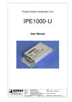
1
User Manual
IPE16000-USB
Version: 1.1
Date: 06.12.2013
GEMAC - Gesellschaft für
Mikroelektronikanwendung Chemnitz mbH
Zwickauer Straße 227
09116 Chemnitz
Germany
Phone:
Fax:
E-Mail:
Web:
+49 371 3377 - 0
+49 371 3377 - 272
[email protected]
www.gemac-chemnitz.de
Revision Overview
Revision Overview
Date
Revision
Change(s)
01.02.2013
1.0
First version
06.12.2013
1.1
Modification Overview features
© Copyright 2013 GEMAC – Gesellschaft für Mikroelektronikanwendung Chemnitz mbH
Subject to change without prior notice.
Our policy is one of continuous improvement, and consequently the equipment may vary slightly from the
description and specifications in this publication. The specifications, illustrations and descriptions provided in
this documentation are not binding in detail.
No part of this publication may be reproduced in any form, or by any means, without the prior written permission of GEMAC – Gesellschaft für Mikroelektronikanwendung Chemnitz mbH.
All rights according to copyright law expressly reserved to GEMAC – Gesellschaft für Mikroelektronikanwendung Chemnitz mbH.
Document: PR-44120-00_01_HB_E_IPE16000-USB
1
Table of Content
Table of Content
1 Overview.................................................................................................................................................6
2 Features ................................................................................................................................................7
2.1 Ordering Information .......................................................................................................................7
3 Input Signals ..........................................................................................................................................8
3.1 Input Signals ...................................................................................................................................8
3.2 Input Amplifier .................................................................................................................................8
3.3 Signal Correction ............................................................................................................................9
3.4 Reference Signal ............................................................................................................................9
4 Output Signals ......................................................................................................................................10
4.1 RS422 ..........................................................................................................................................10
4.2 Error Signals .................................................................................................................................11
5 Interpolation Rate .................................................................................................................................11
5.1 Analog Interpolation ......................................................................................................................11
5.2 Interpolation Rate GC-IP2000........................................................................................................11
5.3 Edge Interval Setting .....................................................................................................................12
5.4 Glitch Filter ...................................................................................................................................12
6 Specifications .......................................................................................................................................13
7 Configuration of the Connectors ............................................................................................................14
7.1 Signal Input X1, Female ................................................................................................................14
7.2 Signal Output X2, Male..................................................................................................................14
7.3 Signal Output X2, Male with Ordered SPI-Option ...........................................................................15
7.4 USB Interface X3 ..........................................................................................................................15
7.5 Analog Output Header X4, Analog Test Signal Sine/Cosine ............................................................15
7.6 LED...............................................................................................................................................16
8 Configuration of the GC-IP2000 ............................................................................................................16
8.1 Configuration Process ...................................................................................................................16
8.2 Configuration with Software IPE16k-Monitor ..................................................................................17
9 Component Mounting Diagram .............................................................................................................17
9.1 Component plan and Solder Side plan of AIP-Module ....................................................................17
9.2 Component Side IPE-Circuit Board ...............................................................................................18
9.3 Dimensions ..................................................................................................................................18
10 Notes .................................................................................................................................................19
Document: PR-44120-00_01_HB_E_IPE16000-USB
2
List of Tables
List of Tables
Table 1: Overview features ........................................................................................................................7
Table 2: Ordering information .....................................................................................................................7
Table 3: Reference signal intern ...............................................................................................................10
Table 4: Configuration of the reference point ............................................................................................10
Table 5: Configuration of the interpolation rate ..........................................................................................12
Table 6: Minimum edge interval ...............................................................................................................12
Table 7: Configuration of the hysteresis ....................................................................................................13
Table 8: Specifications .............................................................................................................................13
Table 9: Signal input SUB–D 15-pin; female .............................................................................................14
Table 10: Signal output SUB–D 15-pin; male ............................................................................................14
Table 11: Signal output X2 with SPI ..........................................................................................................15
Table 12: USB interface X3.......................................................................................................................15
Table 13: Analog output header X4, analog test signal sine/cosine ............................................................15
Table 14: LED .........................................................................................................................................16
Document: PR-44120-00_01_HB_E_IPE16000-USB
3
List of Figures
List of Figures
Figure 1: Block diagram .............................................................................................................................6
Figure 2: Input signals single-ended ...........................................................................................................8
Figure 3: Differential input signals ..............................................................................................................8
Figure 4: Input signals ...............................................................................................................................8
Figure 5: Signal correction .........................................................................................................................9
Figure 6: Reference signal .........................................................................................................................9
Figure 7: Interpolation output signals ........................................................................................................10
Figure 8: Analog interpolation ...................................................................................................................11
Figure 9: Interpolation rate GC-IP2000 .....................................................................................................11
Figure 10: IPE16k-monitor .......................................................................................................................16
Figure 11: Component plan and solder side plan AIP-Module ...................................................................17
Figure 12: Component side IPE-circuit board ...........................................................................................18
Figure 13: Dimensions .............................................................................................................................18
Document: PR-44120-00_01_HB_E_IPE16000-USB
4
Definitions and Abbreviations
Definitions and Abbreviations
AIP
–
Analog Interpolator Module
AVSS
–
ground analog (GND)
AN
–
square-wave signal A negative
AP
–
square-wave signal A positive
BN
–
square-wave signal B negative
BP
–
square-wave signal B positive
COS
–
cosine signal (P = positive; N = negative)
DVDD
–
supply voltage digital (+5V)
DVSS
–
ground digital (GND)
EN
–
error signal negative
EP
–
error signal positive
REF
–
reference signal (P = positive; N = negative)
RS422
–
EIA-422 (conduction-bound differential serial data transmission)
SENSVDD
–
supply voltage analog (+5V)
Sin
–
sinusoidal signal (P = positive; N = negative)
SPI
–
serial peripheral interface
V0
–
mean voltage
Vpp
–
peak-to-peak voltage
ZN
–
square-wave signal Z negative
ZP
–
square-wave signal Z positive
Document: PR-44120-00_01_HB_E_IPE16000-USB
5
1 Overview
1 Overview
The interpolation unit IPE16000-USB was designed to increase the resolution for incremental position and
angular measuring systems with sinusoidal output signals offset by 90°. The IC inside divides the signal
period up to 16384 times. Incremental encoders with voltage interface can be connected directly. The interpolation unit may operate with both differential and single – ended input signals. The configuration of the
board is possible either via EEPROM, or via USB.
The internal AIP-Module performs a permanent correction of the input signals during operating time and allow a multiplication of the signals to the factor 32. The input signals are subjected to GEMAC's patented internal gain and offset control. The phase displacement of the input signals can be corrected as well. The
quality of the signals issued by the sensors is monitored in the internal interpolation circuit GC-IP2000.
The unit can be connected via the RS422 (TTL) output interface to a standard counter or control. The internal power supply voltage is 5VDC.
In addition, several build in functions of the interpolation circuit GC-IP2000 e.g. switchable analog filter or a
digital hysteresis make the unit an ideal choice for use in control systems.
Block diagram
Figure 1: Block diagram
The IPE16000-USB processes the input signals in two steps. In the first step the analog signals are corrected (0.1Vpp … 4Vpp) and multiplied (up to 32 times). In the second step the signals are transmitted to the
GC-IP2000 circuit. The GC-IP2000 divides the signal period up to 2048 times.
Note:
A detailed description of all functions available can be found in the data sheet of GC-IP2000.
Document: PR-44120-00_01_HB_E_IPE16000-USB
6
2 Features
2 Features
Analog part
Analog input
- Sine / cosine / reference (index) signals; differential or single ended
- Input frequency max. 15kHz
- Automatically adjusted gain (0.1Vpp – 4Vpp)
Digital part
Interpolation rate
(100 / 128 / 200 / 256 / 400 / 500 / 512 / 800 / 1000 / 1024 / 1600 / 2000 / 2048)*(1...8)
Output signals
- 30-bit counter value via USB, serial interface (SPI) optional
- Frequency of edge change (A/B/Z) → maximum 24MHz
- 90° square-wave sequences (A/B/Z)
- Error signal
- Auxiliary signals for sensor adjustment
- RS422 interface
- 5V
Signal correction
- Freely definable supporting point correction (up to 1024 supporting points)
- Patented digital controller for the offset, control range ±10% of standard amplitude
- Patented digital controller for the amplitude and offset
- Digital potentiometer with 40 steps for phase correction; selectable range ±5° or ±10°
- LED control signal
Possibilities of configuration
Either: via USB, EEPROM or if the option is ordered via serial interface (SPI)
Optional SPI (internal interface)
- Compatible to the standard SPI: 16-bit, MSB first
- SPI clock up to 25MHz
- For configuration and measuring value output; not required for trivial systems
- 5V interface
Miscellaneous
Suppression of disturbances
- Selectable analog noise filter
- Digital hysteresis for suppression of the edge noise at the output
Adaptation of IC to subsequent
devices
- Adjustable minimum edge interval at the output
- Behaviour of IC in case of sensor error can be programmed
- Adjustable width zero signal Z of ¼ or 1 period A/B
Table 1: Overview features
2.1 Ordering Information
Product type
Description
IPE16000-USB
Interpolation Unit with AIP-Module and GC-IP2000 (standard configuration)
Article number
PR-44120-00
Table 2: Ordering information
Document: PR-44120-00_01_HB_E_IPE16000-USB
7
3 Input Signals
3 Input Signals
The input signals of the IPE16000-USB are analog voltages (sine / cosine), which have a sine-shaped dependency on the measured value (position or angle). The phase shift between those two analog voltages is
90°, related to one period of the scale. A third input signal serves as the reference point signal which determines the zero point of the scale. All three input signals are processed as differential or single-ended signals.
Figure 2: Input signals single-ended
Figure 3: Differential input signals
3.1 Input Signals
Figure 4: Input signals
3.2 Input Amplifier
The IPE16000-USB has a fully differential input stage which performs a correction of the input signals over a
large voltage range (0.1Vpp to 4Vpp) during operating time. In addition, a multiplication of the input signal can
be configured with a factor from 1 to 32. The synthetic Sine / Cosine signals which are generated on the input stage are fed to the interpolation circuit GC-IP2000. The conditioned and multiplied analog signals in
combination with the interpolation circuit GC-IP2000 reach an interpolation rate of up to 16384.
Document: PR-44120-00_01_HB_E_IPE16000-USB
8
3 Input Signals
3.3 Signal Correction
The input signals are subjected to GEMAC's patented internal gain and offset control. The amplitudes are
controlled in the range between 0.1Vpp and 4Vpp of the standard amplitude. The control range for the offset
of the two signals is ±10% of the nominal amplitude. The phase shift of the input signals can be adjusted
statically by the internal potentiometer in a range of ±5° or ±10°.
Figure 5: Signal correction
3.4 Reference Signal
The reference signal of measuring systems is typically called REF, index point or zero point signal. The reference signal is detected if the voltage on input pin REFP is bigger than voltage on input pin REFN.
Figure 6: Reference signal
Note:
The reference point processing in the IPE16000-USB can be deactivated in the internal configuration if no
detection of the reference signal is needed.
Document: PR-44120-00_01_HB_E_IPE16000-USB
9
3 Input Signals
Register value CFG1 / DISZ
Meaning
0
Reference signal at the output active
1
Reference signal at the output inactive
Table 3: Reference signal intern
Note:
The shape of the Z signal on the output of IPE16000-USB can be adapted for different applications in the
configuration of the interpolation circuit. If one increment is selected for the width of the Z signal, the
Z impulse on the output corresponds exactly to one quarter of the period duration of the signals A and B.
The Z impulse extends over a whole period if four increments are selected.
Register value CFG1 / Z4
Meaning
0
1 increment = ¼ period
1
4 increments = 1 period
Table 4: Configuration of the reference point
4 Output Signals
4.1 RS422
The output signals are phase shifted square wave sequences (as common for incremental measuring transducers) which are counted in single or quadruple evaluation mode. A synchronous Z impulse will be generated when the angle of 45° (also refer to Figure 4) is passed through and when the analog differential input
voltage between REFP and REFN exceeds the positive comparator hysteresis level. If the differential input
voltage is permanently above this level, the reference pulse will be generated once during every signal period. The output signals are differential AP – AN, BP – BN, ZP – ZN.
Figure 7: Interpolation output signals
Note:
The signals A, B and Z are offset in time by 1 increment if the digital hysteresis is activated.
Document: PR-44120-00_01_HB_E_IPE16000-USB
10
4 Output Signals
4.2 Error Signals
An error signal will be generated if the input signals are no longer plausible. The error signal will also be
generated if the input frequency is so high that the square-wave signals are unable to follow, and/or when
the maximum input frequency is exceeded. It is recommended to use the error signal for data processing.
Note:
If the error signal was detected, the current measuring results and the following results should be discarded.
Following elimination of the cause of the error and a reset of the error bit, the reference point has to be
passed for absolute value measurements once again!
5 Interpolation Rate
5.1 Analog Interpolation
As a result of the signal noise ratio a maximum multiplication up to factor 8 is useful. The interpolation rate
of the IPE16000-USB is a result from multiplication of the interpolation rate of the GC-IP2000 and of the
multiplication factor of the input stage.
Figure 8: Analog interpolation
5.2 Interpolation Rate GC-IP2000
Possible interpolation rates (IRATE) which can be selected are 2048, 2000, 1600, 1024, 1000, 800, 512,
500, 400, 256, 200, 128 or 100. The term 'interpolation rate' is here understood as the number of increments into which the sinusoidal/cosinusoidal period of the input signals is divided.
Figure 9: Interpolation rate GC-IP2000
Document: PR-44120-00_01_HB_E_IPE16000-USB
11
5 Interpolation Rate
Interpolation rate
CFG1 – IR(3:0)
2000
0000 (0)
1600
0001 (1)
1000
0010 (2)
800
0011 (3)
500
0100 (4)
400
0101 (5)
200
0110 (6)
100
0111 (7)
2048
1000 (8)
1024
1001 (9)
512
1010 (10)
256
1011 (11)
128
1100 (12)
1000
1101 (13)
1000
1110 (14)
1000
1111 (15)
Table 5: Configuration of the interpolation rate
5.3 Edge Interval Setting
The minimum time interval tpp at which the output signals A,B and Z may switch can be adjusted in binary
steps between 1/fOSZ and 128/f OSZ. This function can be used to restrict the bandwidth of the
IPE16000-USB for slow RS422-counters.
Min. edge interval tpp
Register CFG1 – TPP(2:0)
Pin CFGTPP
1/f OSZ
000 (0)
VSS
2/f OSZ
001 (1)
VDD
4/f OSZ
010 (2)
V0
8/f OSZ
011 (3)
open
16/fOSZ
100 (4)
32/fOSZ
101 (5)
64/fOSZ
110 (6)
128/f OSZ
111 (7)
Table 6: Minimum edge interval
5.4 Glitch Filter
To suppress the edge noise of the output signals at low input frequencies and standstill, a digital hysteresis
can be activated for the signals A, B and Z. This prevents switching of the outputs with static input signals.
In this case all output signals are delayed by one increment.
Document: PR-44120-00_01_HB_E_IPE16000-USB
12
5 Interpolation Rate
Pin CFGFILT
CFG1 – DHE
CFG1 – Bit 11
Digital hysteresis
VSS
0
1
Don't use this configuration
VDD
1
1
Don't use this configuration
V0
0
0
deactivated
open
1
0
activated
Table 7: Configuration of the hysteresis
6 Specifications
Characteristic values
Recommended operating conditions
Power supply
Min.
4.75 (4.5)
Nom.
Max.
5.0
5.5
1)
Supply current
Internal interface voltage
Mid-voltage V 0BUF
mA
3.3 / 5.0
V
2.25
Output current on V0BUF
- 20
Analog Input Specifications
Min.
Nom.
Input frequency
Phase offset between SIN and COS
Peak to Peak input voltage SINN Û SINP / COSN Û COSP
Phase deviation
Interpolation rates
Minimum interval time A/B signals
Other characteristics
mA
+80
°C
Max.
Unit
15
kHz
°
4
V pp
4.5 / 9
5 / 10
9 / 11
°
25
Min.
MHz
Nom.
Max.
Unit
(100 / 128 / 200 / 256 / 400 / 500 / 512 / 800 / 1000 / 1024 / 1600
/ 2000 / 2048)*(1...8)
1 / fOSZ
128 / fOSZ
ns
187 / fOSZ
ns
± 0.7
155 / fOSZ
Extruded aluminium housing
IP20
Connector
1) The
30
90
Degree of protection
Dimensions
V
1.0
Interpolation accuracy
Propagation delay square-wave outputs (A / B / Z)
2.4
0.1
Oscillator frequency
Interpolation
V
240
2.1
Operating temperature
Unit
SUB–D, 15-pin
55mm x 80mm x 20mm
control ranges and the interpolation accuracy are limited between 4.5V and 4.75V.
Table 8: Specifications
Document: PR-44120-00_01_HB_E_IPE16000-USB
13
7 Configuration of the Connectors
7 Configuration of the Connectors
7.1 Signal Input X1, Female
Pin
Name
Direction
Meaning
1
SINP
Input
2
AVSS
Output
Encoder signal sine positive
3
COSP
Input
4
SENSVDD
Output
5
–
–
–
6
–
–
–
7
REFN
Input
8
–
–
9
SINN
Input
10
AVSS
Output
11
COSN
Input
12
SENSVDD
Output
13
–
–
14
REFP
Input
15
–
–
Encoder ground
Encoder signal cosine positive
Encoder power supply 5V
Encoder signal reference negative
–
Encoder signal sine negative
Encoder ground
Encoder signal cosine negative
Encoder power supply 5V
–
Encoder signal reference positive
–
Table 9: Signal input SUB–D 15-pin; female
7.2 Signal Output X2, Male
Pin
Name
Direction
1
AP
Output
2
DVSS
Input
3
BP
Output
4
DVDD
Input
5
EN
Output
Meaning
Square wave output A positive
Unit power supply ground
Square wave output B positive
Unit power supply 5V
Error output E negative
6
–
–
7
ZN
Output
–
8
nTRGIN
Input with pullup
9
AN
Output
10
DVSS
Input
11
BN
Output
12
DVDD
Input
13
–
–
14
ZP
Output
Square wave output Z positive
15
EP
Output
Error output E positive
Square wave output Z negative
Trigger signal input; falling edge active
Square wave output A negative
Unit power supply ground
Square wave output B negative
Unit power supply 5V
–
Table 10: Signal output SUB–D 15-pin; male
Document: PR-44120-00_01_HB_E_IPE16000-USB
14
7 Configuration of the Connectors
7.3 Signal Output X2, Male with Ordered SPI-Option
Pin
Name
Direction
Meaning
1
MISO
Output
SPI MISO
2
DVSS
Input
3
SEN
Output
Unit power supply ground
SPI SEN
4
DVDD
Input
5
EN
Output
Unit power supply 5V
6
–
–
7
ZN
Output
8
nTRGIN
Input with pullup
9
MOSI
Input
SPI MOSI
10
DVSS
Input
Unit power supply ground
11
BN
Output
12
DVDD
Input
Error Output E negative not used
–
Square wave output Z negative not used
Trigger signal input; falling edge active
SPI SCK
Unit power supply 5V
13
–
–
14
ZP
Output
–
Square wave output Z positive not used
15
EP
Output
Error output E positive not used
Table 11: Signal output X2 with SPI
7.4 USB Interface X3
Pin
Name
Meaning
1
+ USB
+5V
2
USBD -
Data -
3
USBD +
Data +
4
ID
5
- USB
–
GND
Table 12: USB interface X3
7.5 Analog Output Header X4, Analog Test Signal Sine/Cosine
Pin
Name
Direction
Meaning
1
SMON
Output
Analog test signal sine
2
CMON
Output
Analog test signal cosine
3
GND
Input
Analog ground for measuring
Table 13: Analog output header X4, analog test signal sine/cosine
Document: PR-44120-00_01_HB_E_IPE16000-USB
15
7 Configuration of the Connectors
7.6 LED
LED
Value
Meaning
Sensor monitor
LD1
LD2
red (LD2 off)
Sensor adjustment necessary / Sensor not connected
green (LD1 off)
Sensor signals valid
Off
IPE16000-USB not working
green
IPE16000-USB working
Power LED
LD3
Table 14: LED
8 Configuration of the GC-IP2000
8.1 Configuration Process
After the reset of the IC GC-IP2000, all registers are initialised with their default values. If an
IPE16000-USB unit with SPI-option is used, it should be noted that during the whole RESET sequence the
Pin MISO/nWAIT is maintained at Low level. Subsequently, the configuration register can be modified via
USB or if the SPI-option was ordered via the serial interface SPI. Therefore, the program “IPE16k-Monitor”
has to be used with the IPE16000-USB unit. After installation according to the manual of the program the
IPE16000-USB must be connected to the PC. (refer also to Figure 10)
Figure 10: IPE16k-monitor
Document: PR-44120-00_01_HB_E_IPE16000-USB
16
8 Configuration of the GC-IP2000
8.2 Configuration with Software IPE16k-Monitor
The following functions differ from the description in the program manual:
The checkbox for LEDMODE should always be empty because the LED Control Mode is not supported by the IPE16000-USB.
9 Component Mounting Diagram
9.1 Component plan and Solder Side plan of AIP-Module
Figure 11: Component plan and solder side plan AIP-Module
Document: PR-44120-00_01_HB_E_IPE16000-USB
17
9 Component Mounting Diagram
9.2 Component Side IPE-Circuit Board
Figure 12: Component side IPE-circuit board
9.3 Dimensions
Figure 13: Dimensions
Document: PR-44120-00_01_HB_E_IPE16000-USB
18
10 Notes
10 Notes
Document: PR-44120-00_01_HB_E_IPE16000-USB
19