1
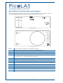
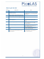
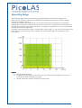
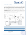
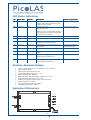
User Manual LDP-C 200-20 Rev. 09.01 valid from June 2009 2009 Table of Contents LDP-C 200-20 ............................................................................................................................. 3 Description of Connections and Jumpers..................................................................................... 4 How to get started ...................................................................................................................... 5 Dos and Don’ts (LDP-C 200-20)................................................................................................... 6 Product Specification................................................................................................................... 7 Operating Range ......................................................................................................................... 8 Functional Description ................................................................................................................. 9 Interface Specification ............................................................................................................... 10 Current Rise Time Adjustment................................................................................................... 11 Effect of Laser Diode Connection on the Pulse Shape................................................................ 11 Test Load .................................................................................................................................. 11 LED Status Indications ............................................................................................................... 12 Absolute Maximum Ratings....................................................................................................... 12 Mechanical Dimensions ............................................................................................................. 12 2 LDP-C 200-20 LDP-C 200-20 Driver for High Power Laser Diodes Output current: 10 .. 200 A Output current between pulses: 0 A Compliance Voltage: 2 .. 20 V Coverage of both cw and qcw range Several protective features Adjustable current rise time Max. Output Power: 4000 W Technical Data:* Output current Max. compliance voltage Typ. pulse rise time (@100 A) Typ. pulse trigger delay Min. pulse duration (@100 A) Max. pulse duration Max. repetition rate (@100 A) Current ripple Current overshoot Current settling time (full-scale) Pulse trigger input Current setting input Figure: Current monitor output, scale: 50A/Div Product Description: The LDP-C 200-20 OEM is a compact high-power current supply to drive almost any kind of Laser Diode. The pulsing capability ranges from single pulses over hundred kilohertz repetition frequency up to continuous operation. Pulses are generated by shorting the output, thus the current between two pulses equals zero. Several analog Inputs and monitor outputs provide an easy way to control the LPD-C. In combination with the PLB-21, the LDP-C 200-20 is capable of generating pulses on its own. No external Pulse generator is required and all parameters can be comfortably adjusted. The innovative current regulation concept of the LDP-C 200-20 produces, compared to the commonly used linear regulation concept, considerably less losses. Current monitor Voltage monitor Supply voltage Dimensions in mm Operating temperature Weight 10 .. 200 A 20 V 0.8 .. 5 µs ** 2 .. 6 µs ** < 5 µs ** cw > 100 kHz ** < 2,5 A, > 20 kHz <5% < 100 ms ** 5 V TTL into 500 Ω PLB-20 0 .. 2 V external (100 A/V) Internal poti PLB-20 100 A/V 0.1 V/V + 24 V DC 145 x 107 x 90 0 to + 55 °C 1582 g * Specifications measured with a fast recovery diode instead of a laser diode. Technical data is subject to change without further notice. ** See User Manual for Details. Designed to shield your laser diode from damage, the LDP-C 200-20 features a number of powerful protective safeguards: Innovative current regulation concept actively prevents laser diode from overshoots and over-current Protection against transients through regulated current rise time Over-temperature shutdown Enable/Disable input Shunt MOSFETs short the output clamps in case of an error Protection of the laser diode against reverse currents 3 Description of Connections and Jumpers The following drawing shows all connections, potis and jumpers which are available to the user. The upper drawing shows the controller, the lower shows the power board. 1 1 RS232 BOB J2 Iset tri se J 1 LED1 LED2 controller board LD+ +24V LD- LD+ LDGND Fan power board RS232 RS232 connector. See page 10 for detailed information. BOB Break-out-board connector. See page 10 for detailed information. Iset Poti for current setpoint (only active when PLB-20 disabled and J1 in position 1-2). Trise Poti for current rise time adjustment. J1 Selects current setpoint input (only active when PLB-20 disabled): 1-2: internal poti; 2-3: external input (BOB connector) J2 PLB-20 communication: 1-2: enable 2-3: disable LED1 Green status LED. See page 12 for detailed information. LED2 Red status LED. See page 12 for detailed information. +24V Supply voltage GND Supply ground LD+ Positive laser diode output (anode). LD- Negative laser diode output (cathode). Do not connect to ground! Fan+ Positive temperature regulated fan output (12 V / 0.4 A) Fan- Negative fan output. Do not connect to ground! 4 How to get started Step # What to do Note 1 Unpack your Device 2 Apply a dummy load at the output (e.g. a Fast-Recovery-Diode) 3 Turn the output-current setpoint poti to the lowest value (turn Poti fully counterclockwise) 4 Connect a Pulse source to the triggering Input e.g. 100 µs, 5 V TTL, 100 Hz. 5 Connect your Scope to the diode current monitor output IDiode. Select high impedance termination, trigger on positive rising edge, 500 mV/div. 6 Apply the supply voltage (24 V DC). Make sure that the supply voltage can deliver enough energy to be stable during the pulses. 7 Set enable pin “high” To protect your Laser-Diode the Driver will stay disabled, if the enable Pin is “high” during power-up. 8 Adjust the pulse current value to the desired value. 9 Disconnect the supply, remove the dummy load at the output and assemble the Laser Diode (Polarity!) Turn poti clockwise and observe the current on the oscilloscope. To protect your Laser-Diode the Driver will keep disabled, if the enable Pin is “high” during power-up. Dummy load must be a valid equivalent to a laser diode (e.g. concerning parasitic capacitance) 5 Dos and Don’ts (LDP-C 200-20) Never ground any lead of the output. This will immediately destroy the driver! Never use any grounded probes at the output. This will immediately destroy the driver and the probe! Never make a short at the output. This will not do any harm to the laser driver but will yield in an incorrect current measurement. Always use all four terminals at the driver’s output. This will reduce the stray impedance of the connection and yields better performance of the internal current monitor. Using only two terminals will result in excessive heat production at the terminal itself and may damage driver and cable. Keep connection between power supply and the driver as well as the connection between driver and laser diode as short as possible. Mount the driver on an appropriate heat sink. Attach a fan to the temperature regulated fan output. The fan should cool the heat sink and the driver itself. 6 Product Specification Output current 10 ... 200 A* Current between Pulses 0A Parasitic voltage between poles measured across the terminals < 150 mV Simmer-current Not availiable Current droop during Pulse < 1% Current Ripple during Pulse Typ 2,6 A (50…200A, @10V) Max. compliance voltage 20 V * typ. Pulse rise time < 1 µs ... 5 µs adjustable typ. Pulse trigger delay typ. 2 µs min. Pulse duration typ. 5 µs max. Pulse duration cw Current settling time (full-scale) < 100 ms Pulse trigger input 5 V TTL into 500 S Current setting input Internal (Poti) 0 .. 2 V external (100 A / V) PLB-20 Current monitor 100 A / V Voltage monitor 0.1 V / V Supply voltage + 18 … 26 V DC Fan output voltage 12 V Fan output current 400 mA RS232 Yes Compatible to PLB-20 Yes Dimensions in mm 145 x 107 x 90 Operating temperature 0 to + 55 ° C * See page 8 for information about the useful operating range. 7 Operating Range The following diagram shows the operating range regarding pulse-current and -voltage of the LDP-C 200-20. The best performance is achieved with currents above 40 A and compliance voltage between 2 V and 20 V (area a) ). Compliance voltages in the range from 4 V to 20 V will result in the best performance. Compliance voltages below 4 V yield in longer tail currents, above 20 V result in a current droop at the beginning of the pulse. Both will not do any harm to the driver. A compliance voltage below 1 V is not recommended and may do harm to the laser diode. An output current below 40 A results in a relative high current ripple ( c) ). This won’t do any harm to the driver but is for some applications not acceptable. For currents below 40A we recommend e.g. the LDP-C 40-05. Legend: Legend a) Area of best performance. b) Compliance-voltages below 4 V and above 20 V will cause a longer tailing of the current or a current droop at the beginning of the pulse. c) Currents below 40 A result in relative high current ripple. 8 Functional Description The LDP-C 200-20 operates by the following principle: A buck converter (S1, S2, D1, D2, LH) generates a current in its inductor LH. This current is shorted to ground through the shunt MOSFET S3. During a pulse, S3 is open and the current flows through the laser diode LD. The inductor current through LH is measured with RS1, this allows the control circuit to regulate the current to a constant value under all circumstances. The laser diode current is measured with RS2. Blocking capacitors decouple the driver from the power supply. C2 filters the high frequency ripple of the buck converter, C1 provides the pulse energy. Inductor current, laser diode current and compliance voltage are preprocessed and then lead to an external connector. A trigger input for generating pulses as well as an enable-input is available. An RS232 interface allows communication with a PLB-20 or a PC. The integrated microcontroller is capable of generating pulses with a configurable repetition rate and duration on its own, but also allows throughput of the external trigger input. Several security features protect the laser diode and driver from damage. The microcontroller supervises driver temperature, inductor current, input and output voltage and disconnects the driver from the power supply in case of an error by opening the security switch S0. D3 protects the laser diode from reverse currents; bypass diode D4 protects the driver in case of a load failure. Element Function S0 Security Switch C2, S1, S2, D1, D2 Buck Converter S3 D3, D4 Shunt Mosfets Short Output LD-Protection RS1 Current sensor for Regulation (Control) RS2 LD-current monitor θ µC Temperature-sensor RS232-communication Temperature-supervision Current-control 9 Interface Specification The following figure shows the input and output stages of the external analog connector. The monitoring outputs are filtered and buffered to improve signal quality. Digital inputs (enable and pulse-trigger) are filtered to reduce spikes and then evaluated by Schmitttriggers to ensure proper evaluation. The external current setpoint input is filtered and then sampled by the microcontroller. All inputs are protected by clamping diodes against over voltage. An auxiliary high impedance 5 V supply voltage is provided to power e.g. the LDP-C BOB. Isetpoint 2.2kΩ 5V1 1nF 100kΩ Idiode 470Ω Iinductor 470Ω 470Ω 220pF 10kΩ 100pF enable 470Ω 5V1 10 9 8 7 6 5 1.2nF 22kΩ pulse Control & 470Ω 5V1 1.2nF 22kΩ 4 3 2 1 GND n.c. 5V 33Ω 470Ω UD iode 220pF The RS232 interface is mainly designed to communicate with the PLB-20. Thus it contains two additional supply voltages to power the PLB-20. 10 Current Rise Time Adjustment The LDP-C 200-20 provides current rise time adjustment of the positive edge of a pulse. When the shunt switch S3 closes, the inductor current through LH commutates from S3 to the output. There it has to magnetize the parasitic inductance Lcable of the cabling between pulser and laser diode. During this process, the current through the laser diodes rises. The time during which the laser diode current rises depends on the voltage difference between the output of the pulser and the laser diode compliance voltage, the current through LH and the parasitic inductance itself. Obviously higher parasitic inductance result in slower current rise and thus higher rise time. Equally a higher current results in a higher rise time. With a higher compliance voltage, the voltage difference between pulser output and laser diode decreases and though the rise time increases. With the poti trise on the controller board, the user can influence the voltage rise of the output voltage of the pulser and thus the rise time of the laser diode current. However, as the rise time depends mainly on the cabling as well as on the chosen current and compliance voltage of the load, no absolute relation for the current rise time can be given. Effect of Laser Diode Connection on the Pulse Shape Parasitic elements in pulser and connection line to the laser diode have an important influence on pulse shape and rise time. The parasitic output capacitance of the pulse Cpar, the cabling inductance Lcable and the parasitic capacitance of the diode Cdiode form a resonant circuit. Applying a step function (which is done at the beginning of a pulse) on a resonant circuit results in oscillations and current overshoot. As these oscillations are inacceptable for most laser applications, the parasitic capacitances and inductances have to be minimized. Laser diodes usually have a very low parasitic capacitance in the order of some 10 pF. Together with a short and low inductive connection between laser diode and driver no oscillations or overshoot should occur. In addition, the adjustable current rise time helps to avoid overshoot and oscillations. A very short rise time and thus a very high current rise results in a strong excitation of the resonant circuit. With a longer rise time and softer current rise the resonant circuit is considerably less excited and though oscillations and overshoot will not appear. As already mentioned above, Lcable influences the current rise time at the beginning of the pulse. Because Lcable has to be magnetized up to the inductor current which flows through LH, a higher Lcable yields in a longer rise time. At the end of a pulse S3 closes and shorts the output. Then Lcable has to be demagnetized. At this time, only a very low voltage is available at the output. The time required to demagnetize Lcable depends only on its value. Higher Lcable results in a longer current fall time. Test Load A common method to test the driver is to connect a regular silicon rectifier diode to the driver output. Here has to be paid attention to the junction capacitance of the diode. Only fast recovery diodes (or similar) have a low parasitic capacitance as laser diodes have. To achieve reasonable test results, the parasitic elements of the test diode and the connection must be very similar to a laser diode approach. Regular silicon rectifier diodes have a junction capacitance of several microfarads and are not a suitable test load! The use of these diodes will yield in incorrect current measurement at the pulse edges! 11 LED Status Indications Nr. Green LED Red LED Description Solution (if applicable) 01 Cont. On Off Ready for operation, a pulse at the Trigger input will be followed by the reaction at the output 02 Flashes 2x Off System power up Running self-test If device is not continuously on after a few seconds, the power supply might be too low or too high. 03 Flashes 3x off Enable not connected 10 Cont. On Cont. On Temperature above chosen Maximum Let device cool down 11 Cont. On flashes 1x Device is cooling after switching off because of over-temperature Let device cool down 12 Cont. On flashes 2x Temperature approaching switch-offtemperature Potentially: additional cooling with a fan 13 Don´t care flashes 3x Internal Fault, DAC not addressable Repair needed 14 Don´t care flashes 4x Internal Fault, Temperature-sensor failed Repair needed 15 flashes 2x flashes 5x Minimum Voltage Fault Power supply is below 18 V Adjust power supply 16 flashes 2x flashes 6x Overvoltage Fault Power supply exceeds 27 V Adjust power supply Absolute Maximum Ratings Supply voltage range (Vcc): +18 (UVLO) to +27 V (OVLO) Input current: 200 A Laser diode output current: 210 A Laser diode output voltage: Vcc – 2 V Pulse repetition rate: 200 kHz BOB-connector input and output voltages: 0 V to 5 V BOB-connector output currents: 1 mA Auxiliary 5 V supply voltage output current: 30 mA RS232-connector: +/- 30 V Fan output current: 500 mA (fused) Operating temperature: 0-55 °C Mechanical Dimensions 12 Check power supply