1
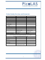
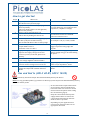
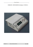
User Manual
LDP-C 18-05
LDP-C 40-05
Rev. 1404
LDP-CW 18-05
LDP-CW 40-05
This manual is for all of the above pulsed C and continuous current CW laser diode
drivers. The CW version is identical to the C version but with a fixed pulse width of
infinity.
Before powering on your unit, read this manual thoroughly and make sure your
understood it fully.
If you have any doubt or suggestion, please do not hesitate to contact us!
PicoLAS GmbH
Company for Innovative Power Electronics and Laser Technology
Kaiserstrasse 100
52134 Herzogenrath
Table of Contents
Table of Contents .................................................................................................................................................................. 2
Product family Overview and Parameters................................................................................................................. 3
LDP-C Capacitor bank:........................................................................................................................................................ 4
Description of Connections and Jumpers................................................................................................................... 5
How to get started ................................................................................................................................................................ 6
Dos and Don’ts (LPD-C 40-05, LDP-C 18-05) ........................................................................................................... 6
Functional Description ....................................................................................................................................................... 7
Interface Specification ........................................................................................................................................................ 8
Active Current Limit ............................................................................................................................................................ 8
Active Current Limit ............................................................................................................................................................ 9
Current Rise Time Adjustment (applies to LDP-C Series only)........................................................................ 9
Effect of Laser Diode Connection on the Pulse Shape (applies to LDP-C Series only) .........................10
Test Load ................................................................................................................................................................................10
Analog Modulation .............................................................................................................................................................10
Power Supply........................................................................................................................................................................11
Soft Start .................................................................................................................................................................................11
Cooling .....................................................................................................................................................................................11
Over Temperature Shutdown .......................................................................................................................................12
Absolute Maximum Ratings ...........................................................................................................................................12
Mechanical Dimensions ...................................................................................................................................................12
Please pay attention to all safety warnings!
Symbols used in this Manual:
Risk of electrical hazard
Please pay special attention
Do not
Valuable information, remark
2
LDP-C 18-05
Product family Overview and Parameters
Technical Data
Output Current Range
Compliance Voltage
Maximum Output Power
Power Dissipation
Current Ripple
Ripple Frequency
Current Overshoot
Analog Modulation
(5 A peak-peak)
Current Settling Time
(0 ... 100%)
Current Set-point (external)
Current sensing monitor
LD-Voltage sensing monitor
Supply Voltage
Size
Weight
Operating Temperature
LDP-CW 18-05
1 … 18 A
5V
90 W
12 W absolute maximum
< 200 mA
> 400 kHz
< 1%
< 16 kHz
LDP-CW 40-05
1 ... 40 A
5V
200 W
30 W absolute maximum
< 400 mA
> 200 kHz
< 1%
< 16 kHz
< 150 µs
< 60 µs
0 … 0.72 V (25 A/V)
25 A/V
0.1 V/V
4 … 6 V DC min 1 V above
compliance voltage
60.9 x 57.8 x 26.3
Half-brick size
154 g
0 ... +55 °C
0 ... 1.6 V (25 A/V)
25 A/V
0.1 V/V
4 … 6 V DC min 1 V above
compliance voltage
60.9 x 57.8 x 26.3
Half-brick size
154 g
0 +55 °C
The table below shows the parameters of the LDP-C series that differ
from the corresponding LDP-CW series units
LDP-C 18-05
LDP-C 40-05
Pulse Current Rise-time
400 ns ... 1 µs adjustable
400 ns ... 1 µs adjustable
Pulse Trigger Delay
200 ns
200 ns
(typical)
Min/Max Pulse Duration
< 1 µs to CW
< 1 µs to CW
Pulse Repetition Rate
single shot to 500 kHz
single shot up to 50 kHz
(Frequency)
Pulse Trigger Input
5 V TTL into 500 Ω
5 V TTL into 500 Ω
Size
60.9 x 57.8 x 54.0
60.9 x 57.8 x 54-0
(including capacitor bank)
(including capacitor bank)
3
LDP-C 40-05
LDP-C Capacitor bank:
For some pulsed applications your power supply might be too weak. Therefore we add to each LDP-C
diode driver an additional capacitor bank that buffers the power of the supply voltage.
If not needed you can dismount it and save space.
LDP-CW driver
LDP-C driver with capacitor bank
4
Description of Connections and Jumpers
The following drawing shows all connections and potentiometers that are available to the user.
LDP-C BOB
Connector for Break Out Board. See page 8 for detailed information.
Trise
Potentiometer for current rise time adjustment.
+5V
Supply voltage
GND
Supply ground
LD+
Positive laser diode output (anode).
LD-
Negative laser diode output (cathode). Do not connect to ground!
Ilimit
Potentiometer for active current limit
For a more
convenient
use of the
diode driver
(e.g. for
laboratory
use) we
recommend
the optional
available
product LDPC-BOB. Please
see LDP-CBOB manual
for further details.
5
How to get started
Step #
What to do
Note
1
Unpack your device; place it in front of you
like shown on the previous page.
2
Apply a dummy load at the output (e.g. a FastRecovery-Diode).
The Laser Diode output is on the right side,
please note polarity.
Dummy load must be a valid equivalent
to a laser diode (e.g. concerning parasitic
capacitance, compliance voltage)
3
Set the current setpoint input to 0.
This is done by feeding 0 V into Pin 10
Connect a voltage source or a
potentiometer to Pin 10 of the BOB
connector and set it to 0 V.
4
Connect a pulse source to the triggering input
on Pin 6 (only for the LDP-C Series).
For the LDP-CW-drivers Pin 6 is always high.
For example: 100 µs, 5 V TTL, 100 Hz.
5
Connect a scope to the diode current monitor
output IDiode on Pin 9.
Ground is on Pin 3 or Pin 5.
Select high impedance termination,
trigger on positive rising edge, 200
mV/div.
6
Apply the supply voltage. (+5 V DC)
Input for the supply voltage are the two
contacts (screws) on the left, please note
polarity.
Make sure that the supply voltage can
deliver enough energy to be stable during
the pulses.
7
Set enable Pin 7 to “high”.
+ 5 V voltage might be taken from Pin 2
Apply +5 V to Pin 7 of the BOB connector.
8
Adjust the setpoint value to the desired pulse
current. Connect voltage source to Pin 10.
9
Disconnect the supply, remove the dummy
load at the output and assemble the Laser
Diode.
Apply a appropriate voltage to Pin 10.
Scale: 25 A/V. Impedance: 10 kΩ .
Pay attention to the polarity of the laser
diode!
Dos and Don’ts (LPD-C 40-05, LDP-C 18-05)
Never ground any lead of the output. This will immediately destroy the driver!
Never use any grounded probes (e.g. from the oscilloscope) at the output. This will immediately destroy
the driver and the probe!
Do not shorten the output. This will not
do any harm to the laser diode driver
but it will result in an incorrect current
measurement. Exception: when setting
the current limit (page 9).
Keep the connection between power
supply and the driver as well as the
connection between driver and laser
diode as short as possible.
Depending on your application and
power levels, mount the driver on an
appropriate heat sink.
6
Functional Description
The pulsed driver LDP-C 40-05/18-05 and the CW drivers LDP-CW 40-05/18-05 operate by the
following principle: A buck converter (S1, S2, D1, D2, LH) generates a current in its inductor LH. This
current is shorted to ground through the shunt MOSFET S3. During a pulse, S3 is open and the current
flows through the laser diode LD. The inductor current through LH is measured with RS1, this allows
the control circuit to regulate the current to a constant value under all circumstances. The laser diode
current is measured with RS2. Blocking capacitors decouple the driver from the power supply. C1
filters the high frequency ripple of the buck converter.
Inductor current, laser diode current and compliance voltage are pre-processed and then lead to the
external BOB-connector. A trigger input for generating pulses and an enable-input as well as s status
output are available.
Several security features protect the laser diode and driver from damage. D3 protects the laser diode
from reverse currents; bypass diode D4 protects the driver in case of a load failure. To protect the
laser diode during start-up of the driver, S0 remains opened until the supply voltage has reached a
stable level. In case of an over temperature condition, the control logic disables the driver. A soft-start
mechanism slowly rises the current after an over temperature shutdown or at startup.
Pow er
Supply
C0
C1
Laser
Diode
BOB
Connector
Cont r ol
Operation Principle of LDP-C / LDP-CW diode driver
Element
Function
S0
Security Switch
C1, S1, S2, D1,
D2
Buck Converter
C0
Input Buffer Capacitor
S3
Shunt Mosfets Short Output
D3, D4
LD-Protection
RS1
Current sensor for Regulation (Control)
RS2
LD-current monitor
θ
Temperature-sensor
7
Interface Specification
The following figure shows the input and output stages of the external analog BOB connector.
The monitoring outputs (Pin 8 and Pin 9) are filtered and buffered to improve signal quality.
Digital inputs (enable and pulse-trigger, Pin 7 and Pin 6) are filtered to reduce spikes and then
evaluated by Schmitt-triggers to ensure proper evaluation. Similarly, the external current
setpoint input is filtered. All inputs are protected by clamPing diodes against over-voltage.
The pulser_ok output (Pin1) is high during normal operation and pulled low in case of an over
temperature alert. The word “pulser” here stands for “diode driver”,
An auxiliary stabilized high impedance +5 V supply voltage is provided (Pin2) to power external
devices (e.g. the LDP-C BOB ) or to provide the logic level “high”.
8
Active Current Limit
The LDP-C 40-05/18-05 and LDP-CW 40-05/18-05 provide an active laser diode current limit feature.
With the help of the current limit potentiometer (see pictures on page 5), the user can adjust the
maximum current that can flow through the laser diode. It is an additional safety feature for protecting
your diode from over-current.
To adjust the current limit to the desired value, follow the steps below:
1.
2.
3.
4.
5.
6.
7.
Disconnect any load from the output.
For LDP-C Series only: Disconnect any trigger connected to the trigger input (Pin 6)
Make a short cut across the output screw terminals where you normally connect the
diode (bridge them with a cable or a piece of metal).
Apply
1.6 V = 40 A (for LDP-C(W) 40-05)
0.72 V = 18 A (for LDP-C(W) 18-05 )
to the current setpoint input (Pin 10).
Apply the + 5 V supply voltage (input connectors on the left).
Monitor the inductor current output signal (Pin 8, see drawing on previous page) and
adjust the current limit to the desired value by turning the potentiometer counter
clockwise (left potentiometer in pictures on page 5).
Disconnect power supply and mount a test load (diode) to the driver.
Apply the power supply (and eventually the trigger source (Pin 6) for the LDP-C Series).
Vary the current set-point input and verify the current limit by monitoring the laser diode
current (Pin 9 or Pin 8).
The current limit function is all set and ready for use.
Note: Although the active current limit function is very robust against disturbances, it only works
reliable if the driver is fully functional. Any damage caused e.g. through over voltage at the setpoint
input may harm the current limit function.
Current Rise Time Adjustment (applies to LDP-C Series only)
The LDP-C 40-05/18-05 provides current rise time adjustment of the positive edge of a pulse. When
the shunt switch S3 closes, the inductor current through LH commutates from S3 to the output. There
it has to magnetize the parasitic inductance Lcable due to cables between diode driver and laser diode.
During this process, the current through the laser diode rises. The rise time depends on the voltage
difference between the output of the diode driver and the laser diode compliance voltage, the current
through LH and the parasitic inductance itself. Obviously higher parasitic inductances result in slower
current rise time and thus higher rise times. Equally a higher current results in a higher rise time. With
a higher compliance voltage, the voltage difference between diode driver output and laser diode
decreases and thus the rise time increases.
With the potentiometer trise on the controller board, the user can influence the voltage rise of the
output voltage of the diode driver and thus the rise time of the laser diode current. However, as the
rise time depends mainly on the cabling as well as on the chosen current and compliance voltage of
the load, no absolute relation for the current rise time can be given.
LCable
CC able
Pulser
Cabl e
9
Laser Diod e
Connection between Diode Driver and Laser Diode
Effect of Laser Diode Connection on the Pulse Shape
(applies to LDP-C Series only)
Parasitic elements in diode driver and connection line to the laser diode have an important influence
on pulse shape and rise time. The parasitic output capacitance of the pulse Cpar, the cabling
inductance Lcable and the parasitic capacitance of the diode Cdiode form a resonant circuit. Applying a
step function (which is done at the beginning of a pulse) on a resonant circuit results in oscillations
and current overshoot. As these oscillations are inacceptable for most laser applications, the parasitic
capacitances and inductances have to be minimized.
Laser diodes usually have a very low parasitic capacitance in the order of some 10 pF. Together with
a short and low inductive connection between laser diode and driver no oscillations or overshoot
should occur. In addition, the adjustable current rise time helps to avoid overshoot and oscillations.
A very short rise time and thus a very high current rise results in a strong excitation of the resonant
circuit. With a longer rise time and softer current rise the resonant circuit is considerably less excited
and though oscillations and overshoot will not appear.
As already mentioned above, Lcable influences the current rise time at the beginning of the pulse.
Because Lcable has to be magnetized up to the inductor current which flows through LH, a higher Lcable
yields in a longer rise time. At the end of a pulse S3 closes and shorts the output. Then Lcable has to be
demagnetized. At this time, only a very low voltage is available at the output. The time required to
demagnetize Lcable depends only on its value. Higher Lcable results in a longer current fall time.
Test Load
A common method to test the driver is to connect a regular silicon rectifier diode to the driver
output. Do not connect to a resistive load, output voltages are too high!
For the LDP-C Series attention has to be paid to the junction capacitance of the diode. Only fast
recovery diodes (or equivalents) have as low a parasitic capacitance as laser diodes have. To
achieve reasonable test results, the parasitic elements of the test diode and the connection must be
very similar to the laser diode approach. Regular silicon rectifier diodes have a junction capacitance
of several microfarads and are not a suitable test load! The use of these diodes will yield in incorrect
current measurement at the pulse edges!
Analog Modulation
The LDP-CW 40-05, LDP-CW 18-05 and the LDP-C 40-05, LDP-C 18-05 are all capable of modulating
the output current controlled via the current set-point input (Pin 10).
The maximum modulation frequency depends on the modulation amplitude of the current. With
higher modulation amplitudes lower frequencies will be achieved and vice versa. Best modulation
results are achieved when the laser diode compliance voltage equals half the supply voltage.
Analog modulation for LDP-CW series
Analog modulation for LDP-C series
10
70
30
60
25
Modulation Frequency
Modulation Frequency
Analog Modulation capability of LDP-C(W) 40-05 (left) and LDP-C(W) 18-05 (right)
50
40
30
20
20
15
10
5
10
0
0
2
5
10
20
2
40
5
10
15
18
Am plitude Modulated Current
Am plitude Modulated Current
The above graphs show the modulation requency in dependence of the setpoint modulation
amplitude. The frequency values where determined at the point where the output current amplitude
dropped to 90% of the setpoint modulation amplitude.
Power Supply
To obtain a good pulsing performance with the LDP-C 40-05/18-05 and the LDP-CW-40-05/18-05, the
drivers require an appropriate power supply unit (PSU). The PSU has to supply the power that is
delivered to the laser diode and also to make up for the losses in the driver itself. It has to be taken
into account that the laser diode power varies strongly when the diode is pulsed or the output current
is modulated. Although the drivers are usually equipped with a large input capacitance of 23.5 mF to
buffer these power peaks, the power supply has to deliver the required power fast enough to avoid
input voltage drops. For excessive pulsing or modulation of the output current, the PSU output
impedance as well as the line impedance between PSU und diode driver has to be as low as possible.
When the input voltage drops below 2.5 V the driver shuts down automatically. This in turn results in
a rise of the input voltage and the driver starts working again. This will cause the input voltage to drop
again if the PSU is too weak to deliver the required power. The result is an unwanted oscillation of the
input voltage and thus a malfunction of the driver. A further protection against these oscillations is the
soft start mechanism at power-up.
Soft Start
The LDP-C 40-05/18-05, LDP-CW 40-05/18-05 drivers apply a soft start mechanism that is activated
upon power-up and after an over temperature alert. This mechanism ramps up the active current limit
from 0 A (at the beginning) to the configured current limit value with a speed of approx. 2 A/ms. This
protects the power supply from excessive current peaks, if the diode driver is already enabled and a
pulse is applied at the trigger input during power up.
Cooling
The LDP-C 18-05 and the LDP-CW-18-05 produce up to 12 W of losses. Thus the base plate has to be
mounted on a heat sink to ensure proper operation and prevent an over temperature shutdown.
In case of the LDP-C 40-05 and LDP-CW-40-05 some more attention has to be paid to the cooling. The
maximum power dissipation here is up to 30 W. With currents above 30 A not only the base plate has
to be cooled properly, but also the power inductor on the board. This can be achieved easily by placing
the driver with its heat sink into the air current of a fan.
Safety Warning: Please be aware that in rare cases the driver could heat up. Please be
cautious not to touch high temperature surfaces!
11
Over Temperature Shutdown
To protect the laser diode and the driver, the unit automatically disables itself if the temperature rises
above 80 °C. This condition is not latched and the diode driver will start working as soon as the
temperature falls below 75 °C. During the over temperature shutdown, the “pulser_ok” output (Pin 1
on the BOB-Connector) is pulled low.
Absolute Maximum Ratings
Supply voltage range: +2.5 V .. +7,6 V
Maximum input current: 40 A (40-05); 18 A (18-05)
Maximum laser diode output current: 40 A (40-05); 18 A (18-05)
Maximum laser diode compliance voltage: 5 V
Maximum pulse repetition rate: 500 kHz (applies to the LDP-C series only)
BOB-connector input and output voltages: 0 V to 5 V
BOB-connector output currents: 1 mA
Auxiliary 5 V supply voltage output current: 30 mA
Operating temperature: 0 - 55 °C
Mechanical Dimensions
Mount holes diameter: 3,2 mm
Over all height (without C-Bank): 27,0 mm
Over all height incl. C-Bank: 54,0 mm
All dimensions in mm
12