1
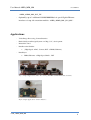
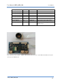
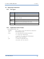
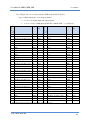
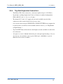
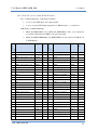
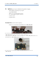
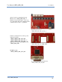
v2.1 020414a
User Manual AHED_MFB_MB
User Manual
AHED_MFB_MB
www.ah-ed.com
[email protected]
Revision: 2.1
Date: 02.04.2014
HW-Revision: v1_1
Fig.1. Top side view of AHED_MFB_MB
Overview
“AHED_MFB_MB” is a board designed around a Xilinx Spartan-6 LXT device in FGG484 package.
It features one Gbit/s Ethernet PHY, two 100 Mbit/s Ethernet PHYs, two independent 16-bit wide
DDR3 SDRAMs and a 32 Mbyte Quad-SPI Flash. In principle, all densities of the Spartan-6 LXT
FPGA, beginning with the LXT25 up to the LXT150 can be assembled on the board.
Expansion connectors are provided at bottom and top side. The top side expansion connectors include
up to 4 lanes of the Multi Gigabit Transceivers MGTs ( for serial connectivity up to 3.2 Gbit/s ) with
3 of the dedicated differential clock inputs made available, as well.
There is an additional FFC connector for attaching an optional Megapixel CMOS image sensor board
“AHED_CAM_ADAPT_EV76C560_CS”.
Up on request reference designs ( FPGA netlist + C-code ) for the on-board components can be made
available by AHED.
AUM_AHED_MFB_MB
1
User Manual AHED_MFB_MB
v2.1 020414a
Fig.2: Top side view next to bottom side view of “AHED_MFB_MB”
Key Features
-
Spartan-6 LXT FPGA ( XC6SLX25T, XC6SLX45T, XC6SLX75T,
XC6SLX100T or XC6SLX150T )
-
Two (XC6SLX25T ) or four ( XC6SLX45T to XC6SLX150T ) MGT lanes are
made available via the top side expansion connectors allowing for serial highspeed connectivity like PCI express, SATA, DisplayPort or High-Speed
ADCs/DACs with JESD204 interface
-
1x 10/100/1000 Mbit/s tri-speed Gigabit Ethernet PHY ( Marvell 88E1111 ),
magnetics and RJ45 Jack onboard
-
2x 10/100 Mbit/s Ethernet PHY ( SMSC LAN8720A ), magnetics and RJ45 Jacks
onboard
-
2x 16-bit wide 1Gbit ( 128 Mbyte ) DDR3 SDRAM
-
1x Quad SPI NOR Flash 256Mbit ( 32 Mbyte )
-
JTAG connector ( with included adapter compatible to standard Xilinx JTAG
cable )
-
For XC6SLX75T, XC6SLX100T or XC6SLX150T bitstream encryption
( AES256 ) with onboard battery for volatile key in SRAM
-
Each Spartan-6 FPGA includes a unique 56-bit “Device-DNA” for unambiguously
identifying a board. Apart from that the Spansion SPI flash features a One Time
Programmable ( OTP ) array of 1024 bytes
-
Bottom side expansion connectors ( 2x FX8C-60P-SV6 )
•
Hirose FX8-Series, up to 3.125 Gbit/s, in principle stacking heights from 5
mm to 16 mm ( in standard configuration 11 mm or 16 mm )
AUM_AHED_MFB_MB
2
User Manual AHED_MFB_MB
•
v2.1 020414a
Power can be supplied to the board via this connectors ( 5 V +- 5%, abs
max 5.5 V )
•
The internal 3.3 V and 1.5 V supply rails are made available to any
external HW
•
-
Up to 31 differential pairs or up to 62 single ended signals
Top side expansion connectors ( 2x FX8C-80S-SV5 )
•
The pinning of both connectors is almost identical to allow them to be used
for two separate extensions or jointly
•
Hirose FX8-Series, up to 3.125 Gbit/s, in principle stacking heights from 5
mm to 16 mm ( in standard configuration 10, 11, 12, 14, or 16 mm )
•
The internal 2.5 V and 3.3 V supply rails are made available on each of the
connectors to the external circuit
•
Up to two MGT lanes with reference clock input are made available on
each of the two connectors
•
-
Up to 30 differential pairs or up to 60 single ended general purpose signals
Clocking
•
The board features a low jitter 125 MHz PCI express clock generator, a 25
MHz low jitter oscillator and a low-power 100 MHz MEMS oscillator all
accessible by the FPGA.
-
Dedicated camera connector
•
The board includes a 34-pin FFC connector for attaching AHED camera
modules
•
-
(optional ) µSD socket
-
Required Power Supply:
•
5V +- 5 %, abs max 5.5 V
•
Power consumption: ~ 2 – 15 W ( depending on the specific configuration/ FPGA
design )
-
Optional DVI input ( up to 1920 x1200 @ 60 Hz ) via top side extension module
“AHED_AHMD_DRL_DVI_RX”
-
Optional DVI output ( up to 1920 x1200 @ 60 Hz ) via top side extension module
AUM_AHED_MFB_MB
3
User Manual AHED_MFB_MB
v2.1 020414a
“AHED_AHMD_DRL_DVI_TX”
-
Optionally, up to 2 additional 10/100/1000 Mbit/s tri-speed Gigabit Ethernet
interfaces via top side extension modules “AHED_AHMD_DRL_E1G_MIC”
Applications
-
Video/Image-Processing, Camera Interface
-
Embedded System Design/ System-on-Chip ( SoC ) development
-
Industrial Control
-
Data Recorder/Grabber
•
-
( High-Speed- ADCs, Camera, DVI -> DDR3, Ethernet )
Data Player
•
DDR3, Ethernet -> High-Speed DACs, DVI
Fig. 3: Sample Application: Video Processing ( DVI-RX and DVI-TX module attached )
Fig.4: Sample Application: Camera Interface
AUM_AHED_MFB_MB
4
User Manual AHED_MFB_MB
v2.1 020414a
Table of Contents
Overview .................................................................................................................................... 1
Key Features ............................................................................................................................... 2
Applications ............................................................................................................................... 4
1. Dimensions/Mechanics ....................................................................................................... 6
2. On-board Power Rails ......................................................................................................... 8
3. Components ........................................................................................................................ 9
3.1. DDR3 SDRAM Memory ................................................................................................ 9
3.2. Flash Memory ................................................................................................................. 9
3.3. Ethernet Interfaces ......................................................................................................... 10
4. Clocking ............................................................................................................................ 13
5. JTAG ................................................................................................................................. 13
6. Camera Interface ............................................................................................................... 14
7. µSD Connector.................................................................................................................. 16
8. Status LEDs ...................................................................................................................... 16
9. FPGA Bank Overview ...................................................................................................... 17
10.
Expansion Connectors ................................................................................................... 18
10.1.
Pin Types ................................................................................................................... 18
10.2.
Explanation of Net Names ......................................................................................... 18
10.3.
Bottom Side Expansion Connectors .......................................................................... 19
10.4.
Top Side Expansion Connectors................................................................................ 22
11.
Constraint File ............................................................................................................... 27
12.
Thermal Behavior .......................................................................................................... 27
13.
Environmental Conditions............................................................................................. 27
14.
Errata ............................................................................................................................. 28
15.
Important Information ................................................................................................... 28
16.
Installation ..................................................................................................................... 28
17.
Default Configurations .................................................................................................. 28
18.
Options .......................................................................................................................... 29
Accessories ( must be ordered separately ) .............................................................................. 29
19.
Legal Notices ................................................................................................................. 32
AUM_AHED_MFB_MB
5
User Manual AHED_MFB_MB
v2.1 020414a
1. Dimensions/Mechanics
-
The actual board has a size of 100 x 60 mm
-
The RJ45 Jacks protrude ~ 3 mm beyond the actual PCB edge
-
With stacking heights of up to 16 mm the Hirose FX8 connectors allow for placing
connectors like ( RJ45, D-Sub, BNC ( low profile ), DVI… ) below this board and allow
placing a top side expansion board directly above this PCB
-
The board has 4 mounting holes with a nominal diameter of 3.2 mm
-
Apart from the expansion connectors and RJ45 Jacks the highest component on the top
side is ~6 mm and ~3 mm on the bottom side.
-
The nominal board thickness of “AHED_MFB_MB” is 1.6 mm
Fig.5: Top side drawing of “AHED_MFB_MB”
AUM_AHED_MFB_MB
6
v2.1 020414a
User Manual AHED_MFB_MB
Fig.6: Bottom side drawing of “AHED_MFB_MB”
Receptacle
FX8C-**>S-SV
FX8C-**>S-SV5
FX8C-**>P-SV
5 mm
10 mm
FX8C-**>P-SV1
6 mm
11 mm
FX8C-**>P-SV2
7 mm
12 mm
FX8C-**>P-SV4
9 mm
14 mm
FX8C-**>P-SV6
11 mm
16 mm
Header
Tab.1: Expansion connector stacking height matrix
AUM_AHED_MFB_MB
7
User Manual AHED_MFB_MB
v2.1 020414a
2. On-board Power Rails1
-
5V
•
external power supply rail
•
+-5 %, abs max 5.5 V, exceeding this ( even if only for short transients ) can
destroy the SMPS ICs (!!!)
•
Needs external bulk capacitance ( e.g. Aluminium 470 µF, >= 10 V, close to the
board )
•
Can either be provided via the right bottom side expansion connector or via
soldering a cable to two pads on the top side
-
3.3 V
•
Internally generated via SMPS from 5V
•
3A
•
Supplies FPGA bank 0 ( routed primarily to expansion connectors top ) and bank
2 and FPGA Vccaux
-
-
-
-
2.5 V
•
Internally generated via SMPS from 5V
•
3A
1.5 V
•
Internally generated via SMPS from 5V
•
3A
•
Supplies FPGA bank 1 and 3 ( DDR3 interface )
1.2 V
•
Internally generated via SMPS from 5V
•
5A
•
Supplies FPGA core and Ethernet PHY cores
1.2 V ( MGT )
•
Internally generated via SMPS from 5V with passive post-filter
•
3A
1
The given current is the rated current of the individual SMPS circuit. The allowed combined power supplied by
all SMPS together might be significantly lower due to thermal limitations
AUM_AHED_MFB_MB
8
v2.1 020414a
User Manual AHED_MFB_MB
3. Components
3.1.
DDR3 SDRAM Memory
-
The board features two 16-bit wide 1Gbit ( 128 Mbyte ) DDR3 SDRAM memory chips.
-
These chips are connected to the dedicated Memory Controller Blocks ( MCBs ) within
the FPGA accessible via bank 1and 3.
-
For detailed pinning information please refer to the constraint file (*.ucf)
3.2.
-
Flash Memory
This board is equipped with a 256 Mbit ( 32 Mbyte ) Quad SPI flash, typically a
S25FL256S device by Spansion
-
In Quad Read DDR mode data transfer rates of up to 66 Mbyte/s can be achieved.
-
Up on request a sample bitstream and Windows application can be provided for writing
bitstream and or processor code into the SPI flash via a UDP connection from a Windows
PC
Net
FPGA
Signal Standard
Description
Pin
SPI_CONFIG_CS
AA3
LVCMOS33
Chip select signal, active low
SPI_CONFIG_CLK
Y20
LVCMOS33
Clock signal from FPGA to SPI Flash
SPI_CONFIG_MISO
AA20
LVCMOS33
DQ1, in 1x mode from SPI Flash to
FPGA
SPI_CONFIG_MISO2
R13
LVCMOS33
WPn/VPP/DQ2, required for 4x
interface
SPI_CONFIG_MISO3
T14
LVCMOS33
HOLDn/DQ3, required for 4x interface
SPI_CONFIG_MOSI
AB20
LVCMOS33
DQ0, in 1x mode from FPGA to SPI
flash
Tab.2: SPI Flash signal connection
AUM_AHED_MFB_MB
9
v2.1 020414a
User Manual AHED_MFB_MB
3.3.
Ethernet Interfaces
3.3.1.
1000 Mbit/s
-
Implemented via a Marvell Alaska Ethernet PHY chip ( 88E1111 )
-
Attached in RGMII mode
-
PHY MII address: 0b10000
-
Magnetics and RJ45 Jack on board -> ready to use, accessible via left RJ45 Jack
-
Up on request a reference design ( netlist + C-code ) attaching the PHY to a MAC and via
DMA to a MicroBlaze soft-core processor can be provided
Net
FPGA Pin
Signal Standard
Description
ETHER_Reset_out
M7
LVCMOS15 with
HW reset for Gigabit Ethernet
external pull up to 3.3V
PHY, active low
LVCMOS33
MII interface ( shared for all 3
MDC
AB19
on-board PHYs )
MDIO
D3
LVCMOS33
MII interface ( shared for all 3
on-board PHYs )
EtherA_INTin
K7
LVCMOS33
Interrupt from Gigabit Ethernet
PHY
EtherA_Data_out[0]
T7
LVCMOS33
EtherA_Data_out[1]
U6
LVCMOS33
EtherA_Data_out[2]
W9
LVCMOS33
EtherA_Data_out[3]
Y8
LVCMOS33
EtherA_Data_EN
Y12
LVCMOS33
EtherA_CLK_out
W12
LVCMOS33
EtherA_Data_in[0]
D2
LVCMOS33
EtherA_Data_in[1]
D1
LVCMOS33
EtherA_Data_in[2]
F3
LVCMOS33
EtherA_Data_in[3]
E4
LVCMOS33
EtherA_DV
C1
LVCMOS33
EtherA_CLK_in
Y13
LVCMOS33
RGMII TX clock
RGMII RX clock
Tab.3: Gigabit/s Ethernet signal connection
AUM_AHED_MFB_MB
10
v2.1 020414a
User Manual AHED_MFB_MB
3.3.2. 100 Mbit/s
-
Two interfaces ( A ) and ( B )
-
Implemented via a SMSC Ethernet PHY chip ( LAN8720A )
-
Attached in RMII mode
-
PHY MII address: 0b00000 ( A ), 0b00001 ( B )
-
Magnetics and RJ45 Jacks on-board -> ready to use, accessible via right RJ45 Jack (A)
and middle RJ45 Jack (B)
-
Up on request a reference design ( netlist + C-code ) attaching the PHYs to MACs and via
DMA to a MicroBlaze soft-core processor can be provided
Net
FPGA
Signal Standard
Description
LVCMOS33
Shared tnterrupt from both100 Mbit
Pin
E100_INT_n
D21
PHYs
E100_RST_n
Y3
LVCMOS15 with
HW reset for both 100 Mbit/s PHYs,
external pull up to
active low
3.3V
E100_A_RX_CRS_DV
N16
LVCMOS33
E100_A_RX_ER
P16
LVCMOS33
E100_A_RX_Din[0]
T20
LVCMOS33
E100_A_RX_Din[1]
U19
LVCMOS33
E100_A_Clkout
V17
LVCMOS33
50 MHz RMII clock generated by
FPGA
E100_A_TX_EN
W18
LVCMOS33
E100_A_TX_Dout[0]
Y17
LVCMOS33
E100_A_TX_Dout[1]
U19
LVCMOS33
E100_B_RX_CRS_DV
J16
LVCMOS33
E100_B_RX_ER
J17
LVCMOS33
E100_B_RX_Din[0]
M18
LVCMOS33
E100_B_RX_Din[1]
M17
LVCMOS33
E100_B_Clkout
U13
LVCMOS33
50 MHz RMII clock generated by
FPGA
E100_B_TX_EN
AUM_AHED_MFB_MB
U14
LVCMOS33
11
v2.1 020414a
User Manual AHED_MFB_MB
E100_B_TX_Dout[0]
AA18
LVCMOS33
E100_B_TX_Dout[1]
AB18
LVCMOS33
Tab.4: 100Mbit/s Ethernet signal connection
3.3.3. Extension
-
Modules
Up to 2 additional 1000 Mbit/s Ethernet interfaces can be added via the top side expansion
connectors ( see Gbit/s Ethernet module “AHED_AHMD_DRL_E1G_MIC” )
AUM_AHED_MFB_MB
12
v2.1 020414a
User Manual AHED_MFB_MB
4. Clocking
-
The main clock source of this board is a low jitter PCI express clock generator, providing
125 MHz differentially to the FPGA2
-
This clock signal is the basis for designs using the DDR3 SDRAM or the MGTs and can
be used to derive clocks for internal processing by means of the PLLs within the Spartan-6
FPGA, as well
-
There is a separate low jitter 25 MHz clock oscillator on-board that provides a 25 MHz
reference clock to the Gigabit Ethernet PHY, the FPGA and the Camera FFC header
-
A further low power MEMS 100 MHz oscillator is present on the board, as well
Net
FPGA
Signal Standard
Description
Pin
clk125_p
T12
LVDS_33
clk125_n
U12
LVDS_33
clk100
AB12
LVCMOS33
CLK_25FPGA
AA12
LVCMOS33
Tab.5: FPGA clocking signal connection
5. JTAG
-
Due to space constraints the boards itself does only have a proprietary 6 pin JTAG
header that connects to the JTAG interface of the Spartan-6 FPGA. However, a
small adapter PCB is provided with this board ( as can be seen e.g. on Fig.7 ) that
makes the JTAG interface mechanically compatible with the standard 14-pin
Xilinx download cable.
-
A soon as top side extension modules are installed the JTAG header might not be
directly accessible anymore. Up on request AHED can provide simple adapter
PCBs that keep the JTAG interface accessible with top side extension modules
installed.
-
2
The 88E1111 is not included in the JTAG chain on this board
By changing two resistors on the board this frequency could be changed to 25 MHz, 100 MHz or 200 MHz
AUM_AHED_MFB_MB
13
v2.1 020414a
User Manual AHED_MFB_MB
6. Camera Interface
-
This board provides a dedicated interface for attaching camera modules by AHED. This
interface can be found at the right side of the board ( as seen from the RJ45 Jacks ) in form
of a 34-pin FFC connector.
-
Most of the pins of this interface are shared with the right bottom side expansion
connector. So these are no longer available for general purpose use as soon as the camera
interface is used
-
By means of the FFC cable the actual camera module/CMOS imager can be separated
from the FPGA board by dozens of centimeters, as can be seen in Fig.7
-
Up on request a reference design ( netlist + C-code ) attaching AHED’s camera module
(“AHED_CAM_ADAPT_EV76C560_CS”) featuring an E2V 1.3 Megasample image
sensor via DMA to a MicroBlaze soft-core processor working on the DDR3 memory can
be provided.
Net
FPGA Pin
Signal Standard3
Camera_Data_clk_A
AB13
LVCMOS33
Camera_CSN_A
C11
LVCMOS33
Description
Chip select for the SPI configuration
interface of the CMOS imager, active
low
Camera_reset_n
AF24
LVCMOS15 with
HW reset to the camera chip, active
external pull up
low
to 1.8 V
Camera_MOSI
B8
LVCMOS33
Part of the SPI configuration interface
of the CMOS imager
Camera_SCK
A8
LVCMOS33
Part of the SPI configuration interface
of the CMOS imager
Camera_MISO
B23
LVCMOS18
Part of the SPI configuration interface
of the CMOS imager
Camera_TRIG_A
A11
LVCMOS33
Camera_Data_A[0]
R19
LVCMOS18
Camera_Data_A[1]
R20
LVCMOS18
Camera_Data_A[2]
T18
LVCMOS18
Camera_Data_A[3]
T19
LVCMOS18
Camera_Data_A[4]
U19
LVCMOS18
Trigger input for image acquisition
3
Those signals with LVCMOS33 go through a lefte shifter before being routed to the FFC connector to match
the 1.8 V requirement of the image sensor
AUM_AHED_MFB_MB
14
v2.1 020414a
User Manual AHED_MFB_MB
Camera_Data_A[5]
V20
LVCMOS18
Camera_Data_A[6]
T20
LVCMOS18
Camera_Data_A[7]
U20
LVCMOS18
Camera_Data_A[8]
U21
LVCMOS18
Camera_Data_A[9]
U22
LVCMOS18
Camera_FEN_A
T22
LVCMOS18
Data interface: Field enable signal
Camera_LEN_A
U23
LVCMOS18
Data interface: Line enable signal
Camera_FLO_A
U17
LVCMOS18
Illumination control output from the
CMOS imager
Tab.6: Camera connector signal connection
Fig.7: Showing camera module “AHED_CAM_ADAPT_EV76C560_CS” with C Mount /CS Mount lens holder
attached to the FPGA board
AUM_AHED_MFB_MB
15
v2.1 020414a
User Manual AHED_MFB_MB
7. µSD Connector
-
There is an optional µSD socket on the bottom side of this board. The connector is
optional in the sense that it shares IOs with the left bottom side expansion connector and is
deactivated ( by means of missing 0-Ohm resistors by default in favor of the bottom side
expansion option )
-
By adding eight 0402 0-Ohm resistors ( can be performed by AHED up on request ) the
µSD socket can be made active
-
The µSD socket cannot be used for the XC6SLX75T device since the required IOs are
not available on this device
Net
FPGA Pin
Signal Standard
Description
SD_CLK
W6
LVCMOS33
SD_DAT0
W8
LVCMOS33
SD_DAT1
V7
LVCMOS33
SD_DAT2
U8
LVCMOS33
SD_DAT3
T8
LVCMOS33
SD_CMD
Y6
LVCMOS33
10k pull up to 3.3 V
SD_SW_A
V9
LVCMOS33
µSD-Connector switch A, 10k pull down
SD_SW_B
U9
LVCMOS33
µSD-Connector switch B, 10k pull up to
3.3 V
Tab.7: µSD socket signal connection
8. Status LEDs
-
Each RJ45 Jack has 2 LEDs for indicating the status of the respective Ethernet interface.
The specific behaviour depends on the configuration of the specific PHY
-
All further LED outputs of the Marvell 88E1111 Gigabit/s Ethernet PHY are connected to
red SMD LEDs on the board
-
There are 3 LEDs indicating the status of the FPGA
•
“INIT_B”: Illuminates red while the FPGA is not configured
•
“DONE”: Illuminates green when the FPGA is configured
•
“AWAKE”:
AUM_AHED_MFB_MB
16
User Manual AHED_MFB_MB
v2.1 020414a
9. FPGA Bank Overview
-
-
-
-
Bank 0:
•
“top” bank
•
Vccio: 3.3 V
•
True LVDS output capable
•
LVCMOS 3.3 V output capable
Bank 1:
•
“right” bank
•
Vccio: 1.5 V
•
LVCMOS output only at 1.5 V
•
LVCMOS input up to 3.3 V
Bank 2:
•
“bottom” bank
•
Vccio: 3.3 V
•
True LVDS output capable
•
LVCMOS 3.3 V output capable
Bank 3:
•
“left” bank
•
Vccio: 1.5 V
•
LVCMOS output only at 1.5 V
•
LVCMOS input up to 3.3 V
AUM_AHED_MFB_MB
17
User Manual AHED_MFB_MB
v2.1 020414a
10. Expansion Connectors
10.1.
Pin Types
Type
Description
GND
Ground pin
PWR
Power supply pin
RFU
Reserved for future use. No assumption must be made on the
connection of this pin
IO
General purpose input/output pin
HSDIO
High Speed Differential IO: Routed as differential pair, closely length
matched, can be used as general purpose IO, as well
GCLK
Global Clock input, can be used as IO or possibly HSDIO, as well
Tab.8: Extension connector pin types
10.2.
Explanation of Net Names
E.g. IC_BB_R_IO_L72N_1_n25
“IC_BB_R”
Type of expansion connector: Here InterConnect to Base Board
“_IO”
Pin is Input/Output capable
“_L72N”
“L72” signal label taken from Xilinx documentation,
“N” -> negative pin of differential pair
( as opposed to “P“ -> positive pin of differential pair )
“_1”
Signal belonging to FPGA Bank 1
“_n25”
not available on LX25T FPGA device
( also possible “_n75” and “_n25_n75” )
AUM_AHED_MFB_MB
18
User Manual AHED_MFB_MB
10.3.
v2.1 020414a
Bottom Side Expansion Connectors
-
Two Hirose FX8-Series connectors ( connector capable of up to 3.125 Gbit/s )
-
In principle, stacking heights from 5 mm to 16 mm ( in standard configuration,
FX8C-60P-SV6, 11 mm or 16 mm )
-
Power can be supplied to the board via this connectors ( 5 V +- 5%, abs max 5.5
V)
-
The internal 3.3 V and 1.5 V supply rails are made available to any external HW,
0.4 A max per contact
-
Care should be taken when the XC6SLX25T or XC6SLX75T FPGAs are supposed to
be used because numerous IOs are not available on these devices ( see
“Explanation of Signal Names” )
AUM_AHED_MFB_MB
19
v2.1 020414a
User Manual AHED_MFB_MB
10.3.1. Left side ( as seen through the PCB from the RJ 45 Jacks )
Up to 17 differential pairs -> 34 single ended IOs
•
7 out of 14 LVDS input and output capable
•
7 out of 14 only LVDS input capable due to FPGA bank ( 1,3 ) restrictions
Type
Connector
Pin
Net
FPGA
Pin
Net
Type
Connector
Pin
-
FPGA
Pin
1
GND
GND
60
1.5 V
PWR
2
3.3 V
PWR
59
1.5 V
PWR
3
3.3 V
PWR
58
GND
GND
4
GND
GND
57
IC_BB_R_IO_L22N_2_n25_n75
IO
T11
5
3.3 V
PWR
56
IC_BB_R_IO_L22P_2_n25_n75
IO
R11
6
3.3 V
PWR
55
GND
GND
7
GND
GND
54
IC_BB_R_IO_L23N_2_n25_n75
IO
U15
8
IC_BB_R_IO_L72N_1_n25
IO
T17
53
IC_BB_R_IO_L23P_2_n25_n75
IO
T15
9
IC_BB_R_IO_L72P_1_n25
IO
R17
52
GND
GND
10
GND
GND
51
IC_BB_R_IO_L4N_2_n25
IO
V15
11
IC_BB_R_IO_L70N_1_n25
IO
R16
50
IC_BB_R_IO_L4P_2_n25
IO
U16
12
IC_BB_R_IO_L70P_1_n25
IO
R15
49
GND
GND
13
GND
GND
48
IC_BB_R_IO_L57N_2_n75
IO
U8
14
IC_BB_R_IO_L25N_3_n25
IO
P7
47
IC_BB_R_IO_L57P_2_n75
IO
T8
15
IC_BB_R_IO_L25P_3_n25
IO
P6
46
GND
GND
16
GND
GND
45
IC_BB_R_IO_L60N_2_n75
IO
Y6
17
IC_BB_R_IO_L7N_3_n25
IO
T5
44
IC_BB_R_IO_L60P_2_n75
IO
W6
18
IC_BB_R_IO_L7P_3_n25
IO
T6
43
GND
GND
19
GND
GND
42
IC_BB_R_IO_L58N_2_n75
IO
W8
20
IC_BB_R_IO_L8N_3_n25
IO
V3
41
IC_BB_R_IO_L58P_2_n75
IO
V7
21
IC_BB_R_IO_L8P_3_n25
IO
V5
40
GND
GND
22
GND
GND
39
IC_BB_R_IO_L50N_2_n75
IO
V9
23
IC_BB_R_IO_L24N_3_n25
IO
T4
38
IC_BB_R_IO_L50P_2_n75
IO
U9
24
IC_BB_R_IO_L24P_3_n25
IO
U4
37
GND
GND
25
GND
GND
36
IC_BB_R_IO_L10N_3
IO
AA1
26
IC_BB_R_IO_L26N_3_n25
IO
R4
35
IC_BB_R_IO_L10P_3
IO
AA2
27
IC_BB_R_IO_L26P_3_n25
IO
T3
34
GND
GND
28
GND
GND
33
IC_BB_R_IO_L9N_3
IO
P4
29
IC_BB_R_IO_L23N_3_n25
IO
N7
32
IC_BB_R_IO_L9P_3
IO
P5
30
IC_BB_R_IO_L23P_3_n25
IO
N6
31
GND
GND
Tab.9: Bottom side expansion connector ( left ) signal connection
AUM_AHED_MFB_MB
20
v2.1 020414a
User Manual AHED_MFB_MB
10.3.2. Right side ( as seen through the PCB from the RJ 45 Jacks )
Up to 14 differential pairs -> 28 single ended IOs
•
11 out of 14 LVDS input and output capable
•
3 out of 14 only LVDS input capable due to FPGA bank ( 1 ) restrictions
Type
Connector
Pin
Net
FPGA
Pin
1
GND
GND
2
IC_BB_L_IO_L20N_2_n75
IO
3
IC_BB_L_IO_L20P_2_n75
IO
4
GND
GND
5
IC_BB_L_IO_L6N_2
IO
6
IC_BB_L_IO_L6P_2
IO
7
GND
GND
8
IC_BB_L_IO_L21N_2
IO
9
IC_BB_L_IO_L21P_2
IO
10
GND
GND
11
IC_BB_L_IO_L19N_2
IO
12
IC_BB_L_IO_L19P_2
IO
13
GND
GND
14
IC_BB_L_IO_L44N_2_n75
IO
15
IC_BB_L_IO_L44P_2_n75
IO
16
GND
GND
17
IC_BB_L_IO_L42N_2_n75
IO
18
IC_BB_L_IO_L42P_2_n75
IO
19
GND
GND
20
IC_BB_L_IO_L46N_2_n75
IO
21
IC_BB_L_IO_L46P_2_n75
IO
22
GND
GND
23
IC_BB_L_IO_L59N_2_n75
IO
24
IC_BB_L_IO_L59P_2_n75
IO
25
GND
GND
26
IC_BB_L_IO_L17N_2_n75
IO
27
IC_BB_L_IO_L17P_2_n75
IO
28
GND
GND
29
IC_BB_L_IO_L18N_2_n75
IO
30
IC_BB_L_IO_L18P_2_n75
IO
Net
Type
Connector
Pin
-
FPGA
Pin
60
5V
PWR
Y14
59
5V
PWR
W14
58
GND
GND
57
5V
PWR
AB14
56
5V
PWR
AA14
55
GND
GND
54
5V
PWR
AB15
53
5V
PWR
Y15
52
GND
GND
51
5V
PWR
AB16
50
5V
PWR
AA16
49
GND
GND
48
-
RFU
Y10
47
-
RFU
W10
46
GND
GND
45
-
RFU
W11
44
-
RFU
V11
43
GND
GND
42
IC_BB_L_IO_L5N_2_n75
IO
Y18
U10
41
IC_BB_L_IO_L5P_2_n75
IO
W17
T10
40
GND
GND
39
IC_BB_L_IO_L71N_1_n25
IO
P18
R8
38
IC_BB_L_IO_L71P_1_n25
IO
P17
R9
37
GND
GND
36
IC_BB_L_IO_L73N_1_n25
IO
T18
W15
35
IC_BB_L_IO_L73P_1_n25
IO
T19
Y16
34
GND
GND
33
IC_BB_L_IO_L58N_1_n25
IO
N15
W13
32
IC_BB_L_IO_L58P_1_n25
IO
M16
V13
31
GND
GND
Tab.10: Bottom side expansion connector ( right ) signal connection
AUM_AHED_MFB_MB
21
User Manual AHED_MFB_MB
10.4.
v2.1 020414a
Top Side Expansion Connectors
-
Two Hirose FX8-Series connectors ( connector capable of up to 3.125 Gbit/s )
-
In principle, stacking heights from 5 mm to 16 mm ( in standard configuration,
FX8C-80S-SV5, 10, 11, 12, 14, or 16 mm )
-
The internal 2.5 V and 3.3 V supply rails are made available on each of the
connectors to the external circuit, 0.4 A max per contact
-
Care should be taken when the XC6SLX25T or XC6SLX75T FPGAs are supposed to
be used because several IOs are not available on these devices ( see “Explanation
of Signal Names” )
-
Up to two MGT lanes with reference clock input are made available on each of the
two connectors
-
All signals are routed as 100 Ohm differential pairs with tight length matching to allow for
data rates up to the maximum of the respective FPGA pins ( 1080 Mbit/s for general
FPGA IOs and 3.2 Gbit/s for MGTs )
AUM_AHED_MFB_MB
22
v2.1 020414a
User Manual AHED_MFB_MB
10.4.1. Left side ( as seen from the RJ 45 Jacks )
-
-
Up to 15 differential pairs -> 30 single ended IOs
•
11 out of 15 LVDS input and output capable
•
4 out of 15 only LVDS input capable due to FPGA bank ( 3 ) restrictions
2 MGT lanes of FPGA Bank 101
•
MGT_TL_REFCLK1P ( C11 )/ MGT_TL_REFCLK1N ( D11 ) are connected to
a low jitter differential 125 MHz on-board clock signal
•
MGT_TL_REFCLK0P/ MGT_TL_REFCLK0N are AC coupled via 100 nF, 16
V X7R MLCCs
FPGA
Pin
1
GND
GND
2
BEXT_L_IO_L58P_3_n25
HSDIO
3
BEXT_L_IO_L58N_3_n25
HSDIO
4
GND
GND
5
BEXT_L_IO_L82P_3_n25
HSDIO
6
BEXT_L_IO_L82N_3_n25
HSDIO
7
GND
GND
8
BEXT_L_IO_L80P_3_n25
HSDIO
9
BEXT_L_IO_L80N_3_n25
HSDIO
10
GND
GND
11
BEXT_L_IO_L81P_3_n25
HSDIO
12
BEXT_L_IO_L81N_3_n25
HSDIO
13
GND
GND
14
BEXT_L_IO_L35P_0
GCLK
15
BEXT_L_IO_L35N_0
GCLK
16
GND
GND
17
BEXT_L_IO_L33P_0
HSDIO
18
BEXT_L_IO_L33N_0
HSDIO
19
GND
20
Net
Type
Connector
Pin
Type
Connector
Pin
Net
FPGA
Pin
80
BEXT_L_IO_L4P_0
HSDIO
E5
H4
79
BEXT_L_IO_L4N_0
HSDIO
E6
G4
78
GND
GND
77
BEXT_L_IO_L2P_0
HSDIO
D4
F5
76
BEXT_L_IO_L2N_0
HSDIO
D5
G6
75
GND
GND
74
BEXT_L_IO_L7P_0
HSDIO
F7
H6
73
BEXT_L_IO_L7N_0
HSDIO
F8
G7
72
GND
GND
71
BEXT_L_IO_L32P_0
HSDIO
G8
J7
70
BEXT_L_IO_L32N_0
HSDIO
F9
H8
69
GND
GND
68
BEXT_L_IO_L34P_0
GCLK
G9
H12
67
BEXT_L_IO_L34N_0
GCLK
F10
G11
66
GND
GND
65
BEXT_L_IO_L3P_0
HSDIO
B2
H10
64
BEXT_L_IO_L3N_0
HSDIO
A2
H11
63
GND
GND
GND
62
BEXT_L_IO_L5P_0
HSDIO
B3
2.5 V
PWR
61
BEXT_L_IO_L5N_0
HSDIO
A3
21
2.5 V
PWR
60
GND
GND
22
GND
GND
59
BEXT_L_IO_L6P_0
HSDIO
C4
23
2.5 V
PWR
58
BEXT_L_IO_L6N_0
HSDIO
A4
24
2.5 V
PWR
57
GND
GND
25
GND
GND
56
BEXT_L_IO_L8P_0
HSDIO
C5
26
3.3 V
PWR
55
BEXT_L_IO_L8N_0
HSDIO
A5
27
3.3 V
PWR
54
GND
GND
AUM_AHED_MFB_MB
23
v2.1 020414a
User Manual AHED_MFB_MB
28
GND
GND
53
-
RFU
29
3.3 V
PWR
52
-
RFU
30
3.3 V
PWR
51
GND
GND
31
GND
GND
50
MGT_TL_TX0P
MGT
B6
32
MGT_TL_RX0P
MGT
D7
49
MGT_TL_TX0N
MGT
A6
33
MGT_TL_RX0N
MGT
C7
48
GND
GND
34
GND
GND
47
MGT_TL_TX1P
MGT
B8
35
MGT_TL_RX1P
MGT
D9
46
MGT_TL_TX1N
MGT
A8
36
MGT_TL_RX1N
MGT
C9
45
GND
GND
37
GND
GND
44
MGT_TL_REFCLK0N
MGT
B10
38
-
RFU
43
MGT_TL_REFCLK0P
MGT
A10
39
-
RFU
42
GND
GND
40
GND
GND
41
-
RFU
Tab.11: Top side expansion connector ( left ) signal connection
AUM_AHED_MFB_MB
24
v2.1 020414a
User Manual AHED_MFB_MB
10.4.2. Right side ( as seen from the RJ 45 Jacks )
-
-
Up to 15 differential pairs -> 30 single ended IOs
•
11 out of 15 LVDS input and output capable
•
4 out of 15 only LVDS input capable due to FPGA bank ( 1 ) restrictions
Up to 2 MGT lanes of FPGA Bank 123
•
MGTs not available for XC6SLX25T
•
MGT_TR_REFCLK0P/ MGT_TR_REFCLK0N are AC coupled via 100 nF, 16 V
X7R MLCCs
FPGA
Pin
1
GND
GND
2
BEXT_R_IO_L21N_1_n25
HSDIO
3
BEXT_R_IO_L21P_1_n25
HSDIO
4
GND
GND
5
BEXT_R_IO_L9N_1_n25
HSDIO
6
BEXT_R_IO_L9P_1_n25
HSDIO
7
GND
GND
8
BEXT_R_IO_L10N_1_n25
HSDIO
9
BEXT_R_IO_L10P_1_n25
HSDIO
10
GND
GND
11
BEXT_R_IO_L20N_1
HSDIO
12
BEXT_R_IO_L20P_1
HSDIO
13
GND
GND
14
BEXT_L_IO_L36N_0
GCLK
15
BEXT_L_IO_L36P_0
GCLK
16
GND
GND
17
BEXT_L_IO_L38N_0
HSDIO
18
BEXT_L_IO_L38P_0
HSDIO
19
GND
20
Net
Type
Connector
Pin
Type
Connector
Pin
Net
FPGA
Pin
80
BEXT_L_IO_L50N_0
HSDIO
A17
K16
79
BEXT_L_IO_L50P_0
HSDIO
C17
L15
78
GND
GND
77
BEXT_L_IO_L63N_0
HSDIO
A18
H17
76
BEXT_L_IO_L63P_0
HSDIO
B18
H16
75
GND
GND
74
BEXT_L_IO_L64N_0
HSDIO
A19
B22
73
BEXT_L_IO_L64P_0
HSDIO
C19
B21
72
GND
GND
71
BEXT_L_IO_L65N_0
HSDIO
A20
C22
70
BEXT_L_IO_L65P_0
HSDIO
B20
C20
69
GND
GND
68
BEXT_L_IO_L37N_0
GCLK
F16
F15
67
BEXT_L_IO_L37P_0
GCLK
E16
F14
66
GND
GND
65
BEXT_L_IO_L49N_0
HSDIO
G15
G13
64
BEXT_L_IO_L49P_0
HSDIO
H14
H13
63
GND
GND
GND
62
BEXT_L_IO_L66N_0
HSDIO
C18
2.5 V
PWR
61
BEXT_L_IO_L66P_0
HSDIO
D17
21
2.5 V
PWR
60
GND
GND
22
GND
GND
59
BEXT_L_IO_L62N_0
HSDIO
D19
23
2.5 V
PWR
58
BEXT_L_IO_L62P_0
HSDIO
D18
24
2.5 V
PWR
57
GND
GND
25
GND
GND
56
BEXT_L_IO_L51N_0
HSDIO
F17
26
3.3 V
PWR
55
BEXT_L_IO_L51P_0
HSDIO
G16
27
3.3 V
PWR
54
GND
GND
AUM_AHED_MFB_MB
25
v2.1 020414a
User Manual AHED_MFB_MB
28
GND
GND
53
-
RFU
29
3.3 V
PWR
52
-
RFU
30
3.3 V
PWR
51
GND
GND
31
GND
GND
50
MGT_TR_TX1P
MGT
B16
32
MGT_TR_RX1P
MGT
D15
49
MGT_TR_TX1N
MGT
A16
33
MGT_TR_RX1N
MGT
C15
48
GND
GND
34
GND
GND
47
MGT_TR_TX0P
MGT
B14
35
MGT_TR_RX0P
MGT
D13
46
MGT_TR_TX0N
MGT
A14
36
MGT_TR_RX0N
MGT
C13
45
GND
GND
37
GND
GND
44
MGT_TR_REFCLK0N
MGT
A12
38
MGT_TR_REFCLK1N
MGT
F12
43
MGT_TR_REFCLK0P
MGT
B12
39
MGT_TR_REFCLK1P
MGT
E12
42
GND
GND
40
GND
GND
41
-
RFU
Tab.12: Top side expansion connector ( right ) signal connection
AUM_AHED_MFB_MB
26
User Manual AHED_MFB_MB
v2.1 020414a
11. Constraint File
-
A constraint file “AHED_MFB_MB.ucf” summarizing the pinning information in this
document is available
12.
Thermal Behavior
-
The thermal behaviour of this board does strongly vary depending on
•
which FPGA is used
•
which components on the board are actually used
•
the specific FPGA design
-
The power consumption can be as low as ~ 2W and could go up to ~ 15 W
-
At ~ 5 – 7 W power consumption the board can be used at an ambient temperature of
25°C without special cooling measures. At higher power levels or higher ambient
temperature cooling measures like forced convection and/or a heat sink on the FPGA are
required. This must especially be considrd with respect to a top side expansion board ( see
e.g. documentation for “AHED_MFB_MB_CB_AHMD_DRL” )
13. Environmental Conditions
-
The junction temperature of no component on the module must exceed 85 °C
-
Usually C-type FPGAs ( commercial grade ) are assembled, however up on request I-type
( industrial grade ) can be used , as well
AUM_AHED_MFB_MB
27
User Manual AHED_MFB_MB
v2.1 020414a
14. Errata
-
None
15. Important Information
16. Installation
17. Default Configurations
-
-
AHED_MFB_MB_STD_LX45-2C
•
Spartan-6 XC6SLX45T, speed grade 2, commercial grade
•
2x 128 Myte DDR3 SDRAM
•
32 Mbyte SPI NOR flash
•
On-board Gigabit Ethernet Interface
•
RJ 45 Jacks assembled
•
Bottom side expansion connectors: 2x FX8C-60P-SV6
•
Top side expansion connectors: 2x FX8C-80S-SV5
•
FFC camera connector assembled
•
µSD socket assembled but not activated
AHED_MFB_MB_STD_LX100-3C
•
Spartan-6 XC6SLX100T, speed grade 3, commercial grade
•
2x 128 Myte DDR3 SDRAM
•
32 Mbyte SPI NOR flash
•
On-board Gigabit Ethernet Interface
•
RJ 45 Jacks assembled
•
Bottom side expansion connectors: 2x FX8C-60P-SV6
•
Top side expansion connectors: 2x FX8C-80S-SV5
•
FFC camera connector assembled
•
µSD socket assembled but not activated
AUM_AHED_MFB_MB
28
User Manual AHED_MFB_MB
v2.1 020414a
18. Options (up on request, minimum order quantities do apply)
-
Different FPGA, industrial grade, speed grade
-
Larger DDR3 SDRAM
-
Without on-board Gigabit Ethernet interface
-
No or other height for expansion connectors
-
No FFC connector
-
No µSD connector
Accessories ( must be ordered separately )
-
Examples of systems build around the FPGA board “AHED_MFB_MB”
Fig.8: Front side view of FPGA board “AHED_MFB_MB” installed on baseboard
“AHED_MFB_BB_LED_SIO32X_A” with top side expansion carrier board
“AHED_MFB_MB_CB_AHMD_DRL” and attached DVI RX module “AHED_AHMD_DRL_DVI_RX” ( left )
and DVI TX module “AHED_AHMD_DRL_DVI_TX” ( right )
Fig.9: Top side view of camera module “AHED_CAM_ADAPT_EV76C560_CS” connected to
“AHED_MFB_MB”
AUM_AHED_MFB_MB
29
v2.1 020414a
User Manual AHED_MFB_MB
A base board is recommended for the
FPGA board “AHED_MFB_MB”. It
features a robust wide range ( 12 V to 24
V ) power input and can be equipped with a
communication module ( e.g. RS232 )
Fig.10. Top side view of
“AHED_MFB_BB_LED_SIO32X_A”
Carrier board needed in case the top side
expansion modules
“AHED_AHMD_DRL_DVI_RX”,
“AHED_AHMD_DRL_DVI_TX” or
“AHED_AHMD_DRL_E1G_MIC” are
supposed to be used on the FPGA board
“AHED_MFB_MB”
Fig.11: Top side view of carrier board
“AHED_MFB_MB_CB_AHMD_DRL”
DVI RX module
“AHED_AHMD_DRL_DVI_RX”
Fig.12: Top side view of DVI RX module
“AHED_AHMD_DRL_DVI_RX”
AUM_AHED_MFB_MB
30
v2.1 020414a
User Manual AHED_MFB_MB
DVI TX module
“AHED_AHMD_DRL_DVI_TX”
Fig.13: Top side view of DVI TX module
“AHED_AHMD_DRL_DVI_TX”
Gigabit/s Ethernet module
“AHED_AHMD_DRL_E1G_MIC”
Fig.14: Top side view of 1Gbit/s Ethernet module
“AHED_AHMD_DRL_E1G_MIC”
Camera headboard for the camera
connector on the FPGA board
“AHED_MFB_MB”
Fig.15. Top side view of camera module
“AHED_CAM_ADAPT_EV76C560_CS”
AUM_AHED_MFB_MB
31
User Manual AHED_MFB_MB
v2.1 020414a
19. Legal Notices
19.1.
No Warranties
The material contained in this document is provided “as is” and is subject to change at any
time without notice.
AHED does not warrant the accuracy and completeness of the materials in this document.
To the maximum extent permitted by applicable law, AHED disclaims any express or implied
warranty of any kind with respect to this document and any information contained herein,
including but not limited to warranties of merchantability, noninfringement of intellectual
property or fitness for any particular purpose.
19.2.
Limitation of Liability
Some states or countries do not allow the exclusion or limitation of implied warranties or the
limitation of special, incidental, or consequential damages, so these limitations and exclusions
may be limited in their application to you. The following limitations apply to the extent
permitted by local law.
In no event will AHED be liable for any damages whatsoever ( including, without
limitation, damages for loss of profits, business interruption or loss of data ) arising out of
the use of or inability to use, or the results of use of this document, any documents linked to
this document, or the materials or information contained at any or all such documents.
AHED shall not be liable for errors or for any special, incidental or consequential damages
arising out of or in connection with the furnishing, use or performance of this document or of
any information contained herein.
If your use of the materials or information contained in this document results in the need for
servicing, repair or correction of equipment or data, you assume all costs thereof.
19.3.
Copyright Notice
AHED explicitly retains all property and intellectual property rights on this document.
Without our explicit consent, the document or any part of it may not be reproduced in any
form or by any means ( including electronic storage and retrieval or translation into a foreign
language )
AUM_AHED_MFB_MB
32
User Manual AHED_MFB_MB
19.4.
v2.1 020414a
Technology Licenses
Hardware, firmware and software described or emntioned in this document is furnished
under a license and may only be used, modified and copied in accordance with the
terms of such a license.
AUM_AHED_MFB_MB
33