1
No. CP-SP-1066E
DIGITRONIK
CPL Communications
DCP31/32
User's Manual
Thank you for the choice of the DIGITRONIK
Digital Program Controller DCP31/32.
This instruction manual not only outlines the
communication functions of the DCP31/32,
but also describes its wiring methods, communication procedure, communication data
table, trouble-shooting, and communication
specifications.
The items required for the DCP 31/32 communication functions to be properly used
are given in this manual.
Persons in charge of design or maintenance
of operation panels or equipment using the
DCP31/32 communication functions should
read this manual without fail.
RESTRICTIONS ON USE
This product has been designed, developed and manufactured for general-purpose
application in machinery and equipment.
Accordingly, when used in applications outlined below, special care should be taken to
implement a fail-safe and/or redundant design concept as well as a periodic
maintenance program.
• Safety devices for plant worker protection
• Start/stop control devices for transportation and material handling machines
• Aeronautical/aerospace machines
• Control devices for nuclear reactors
Never use this product in applications where human safety may be put at risk.
REQUEST
Ensure that this User's Manual is handed over to the user before the
product is used.
Copying or duplicating this User's Manual in part or in whole is forbidden. The information and specifications in this User's Manual are subject to change without notice.
Considerable effort has been made to ensure that this User's Manual is
free from inaccuracies and omissions.
If you should find any inaccuracies or omissions, please contact
Yamatake Corporation.
In no event is Yamatake Corporation liable to anyone for any indirect,
special or consequential damages as a result of using this product.
©1999 Yamatake Corporation ALL RIGHTS RESERVED
The DIGITRONIK® is a registered trademark of Yamatake Corporation.
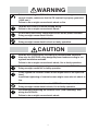
SAFETY PRECAUTIONS
■ About Icons
Safety precautions are for ensuring safe and correct use of this product, and for
preventing injury to the operator and other people or damage to property. You
must observe these safety precautions. The safety precautions described in this
manual are indicated by various icons.
As the following describes the icons and their meanings, be sure to read and
understand the descriptions before reading this manual:
WARNING
CAUTION
Warnings are indicated when mishandling this product might
result in death or serious injury to the user.
Cautions are indicated when mishandling this product might
result in minor injury to the user, or only physical damage to
this product.
■ Examples
Triangles warn the user of a possible danger that may be caused by
wrongful operation or misuse of this product.
These icons graphically represent the actual danger. (The example on
the left warns the user of the danger of electrical shock.)
White circles with a diagonal bar notify the user that specific actions are
prohibited to prevent possible danger.
These icons graphically represent the actual prohibited action. (The
example on the left notifies the user that disassembly is prohibited.)
Black filled-in circles instruct the user to carry out a specific obligatory
action to prevent possible danger.
These icons graphically represent the actual action to be carried out.
(The example on the left instructs the user to remove the plug from the
outlet.)
i
WARNING
Before connecting the DCP31/32 to the measurement target or external
control circuits, make sure that the FG terminal is properly grounded
(100Ω max.).
Failure to do so might cause electric shock or fire.
Turn the DCP31/32 OFF before starting wiring.
Failure to do so might cause electric shock.
Do not touch electrically charged parts such as the power terminals.
Doing so might cause electric shock.
Do not disassemble the DCP31/32.
Doing so might cause electric shock or faulty operation.
CAUTION
Wire the DCP31/32 properly according to predetermined standards.
Also wire the DCP31/32 using designed power leads according to recognized installation methods.
Failure to do so might cause electric shock, fire or faulty operation.
Do not allow lead clippings, chips or water to enter the DCP31/32 case.
Doing so might cause fire or faulty operation.
Firmly tighten the terminal screws at the torque listed in the specifications.
Insufficient tightening of terminal screws might cause electric shock or
fire.
Do not use unused terminals on the DCP31/32 as relay terminals.
Doing so might cause electric shock, fire or faulty operation.
We recommend attaching the terminal cover (sold separately) after
wiring the DCP31/32.
Failure to do so might cause electric shock.
ii
The Role of This Manual
In all, three manuals have been prepared for the DCP31/32. Read the manual according to your specific
requirements. The following lists all the manuals that accompany the DCP31/32 and gives a brief outline of the
manual. If you do not have the required manual, contact Yamatake Corporation or your dealer.
DIGITRONIK Digital Program Controller DCP31 User's Manual
No.CP-UM-1757E
This manual is provided with the DCP31 (single-loop model).
It is required reading for those in charge of designing, producing and
maintaining control systems incorporating the DCP31, and for those using
the DCP31 in other applications.
It describes mounting onto control panels, wiring, parameter setup,
program setup, operation methods, maintenance and inspection,
troubleshooting and specifications.
DIGITRONIK Digital Program Controller DCP32 User's Manual
No.CP-SP-1042E
This manual is provided with the DCP32 (dual-loop model).
It is required reading for those in charge of designing, producing and
maintaining control systems incorporating the DCP32, and for those using
the DCP32 in other applications.
It describes mounting onto control panels, wiring, parameter setup,
program setup, operation methods, maintenance and inspection,
troubleshooting and specifications.
DIGITRONIK CPL Communications DCP31/32 User's Manual
No.CP-SP-1066E
This manual.
This manual is required reading for those using the CPL communications
functions of the DCP31/32.
This manual describes an outline of CPL communications, wiring,
communications procedures and DCP31/32 communications data, how to
remedy trouble, and communications specifications.
iii
Organization of This Manual
This manual is organized as follows.
Chapter 1. COMMUNICATION FUNCTIONS
Communication functions and model numbers of the DIGITRONIK
instruments.
Chapter 2. WIRING
RS-232C and RS-485 wiring methods to make communication between
the DIGITRONIK instuments and other equipment.
Chapter 3. SETTING
Setting for communication of DIGITRONIK instruments.
Chapter 4. COMMUNICATION PROCEDURE
Communication procedure, message configuration, data read/write and
signal timing.
Chapter 5. COMMUNICATION DATA TABLE
Table of various data addresses used for communication of DIGITRONIK
instruments.
Chapter 6. TROUBLESHOOTING
Check points required if the DIGITRONIK instrument communication
should not operate normally.
Chapter 7. SPECIFICATIONS
Communication specifications for the DIGITRONIK instruments.
Appendix
Code table and network configuration using the RS-232C/RS-485
converter CMC10L.
iv
Contents
SAFETY PRECAUTIONS
The Role of This Manual
Organization of This Manual
Contents
Conventions Used in This Manual
Chapter 1.
COMMUNICATION FUNCTIONS
Chapter 2.
WIRING
2-1 RS-485 Connection • • • • • • • • • • • • • • • • • • • • • • • • • • • • • • • • • • • • • • • • • • • • • • • • • • • • • • • • 2-1
■ 5-wire system • • • • • • • • • • • • • • • • • • • • • • • • • • • • • • • • • • • • • • • • • • • • • • • • • • • • • • • • • • 2-1
■ 3-wire system • • • • • • • • • • • • • • • • • • • • • • • • • • • • • • • • • • • • • • • • • • • • • • • • • • • • • • • • • • 2-2
2-2 Terminal Array of DCP31/32 • • • • • • • • • • • • • • • • • • • • • • • • • • • • • • • • • • • • • • • • • • • • • • • 2-3
2-3 Loader Jack• • • • • • • • • • • • • • • • • • • • • • • • • • • • • • • • • • • • • • • • • • • • • • • • • • • • • • • • • • • • • • • • 2-4
Chapter 3.
SETTING
3-1 SETUP Items of DCP31/32 • • • • • • • • • • • • • • • • • • • • • • • • • • • • • • • • • • • • • • • • • • • • • • • • • 3-1
3-2 Initialize • • • • • • • • • • • • • • • • • • • • • • • • • • • • • • • • • • • • • • • • • • • • • • • • • • • • • • • • • • • • • • • • • • • • 3-2
■ Station address • • • • • • • • • • • • • • • • • • • • • • • • • • • • • • • • • • • • • • • • • • • • • • • • • • • • • • • • 3-2
■ Transmission rate / Character format • • • • • • • • • • • • • • • • • • • • • • • • • • • • • • • • • • 3-2
Chapter 4.
COMMUNICATION PROCEDURE
4-1 Outline of Communication Procedure and Messages • • • • • • • • • • • • • • • • • • • • • • 4-1
■ Communication procedure • • • • • • • • • • • • • • • • • • • • • • • • • • • • • • • • • • • • • • • • • • • • • 4-1
■ Configuration of message • • • • • • • • • • • • • • • • • • • • • • • • • • • • • • • • • • • • • • • • • • • • • 4-1
■ Definite examples • • • • • • • • • • • • • • • • • • • • • • • • • • • • • • • • • • • • • • • • • • • • • • • • • • • • • • 4-2
■ Concept of data address • • • • • • • • • • • • • • • • • • • • • • • • • • • • • • • • • • • • • • • • • • • • • • • 4-2
4-2 Data Link Layer • • • • • • • • • • • • • • • • • • • • • • • • • • • • • • • • • • • • • • • • • • • • • • • • • • • • • • • • • • • • 4-3
■ Description of data link layer • • • • • • • • • • • • • • • • • • • • • • • • • • • • • • • • • • • • • • • • • • 4-3
4-3 Application Layer • • • • • • • • • • • • • • • • • • • • • • • • • • • • • • • • • • • • • • • • • • • • • • • • • • • • • • • • • • 4-6
■ Outline of application layer • • • • • • • • • • • • • • • • • • • • • • • • • • • • • • • • • • • • • • • • • • • • 4-6
4-4 Data Read • • • • • • • • • • • • • • • • • • • • • • • • • • • • • • • • • • • • • • • • • • • • • • • • • • • • • • • • • • • • • • • • • • 4-7
■ Description of read request • • • • • • • • • • • • • • • • • • • • • • • • • • • • • • • • • • • • • • • • • • • • 4-7
■ Read response • • • • • • • • • • • • • • • • • • • • • • • • • • • • • • • • • • • • • • • • • • • • • • • • • • • • • • • • • 4-8
■ Expression of decimal numeric (numeric data) • • • • • • • • • • • • • • • • • • • • • • • 4-9
4-5 Data Write • • • • • • • • • • • • • • • • • • • • • • • • • • • • • • • • • • • • • • • • • • • • • • • • • • • • • • • • • • • • • • • • 4-10
■ Description of write request • • • • • • • • • • • • • • • • • • • • • • • • • • • • • • • • • • • • • • • • • • 4-10
■ Write response • • • • • • • • • • • • • • • • • • • • • • • • • • • • • • • • • • • • • • • • • • • • • • • • • • • • • • • 4-11
4-6 File READ/WRITE (program pattern) • • • • • • • • • • • • • • • • • • • • • • • • • • • • • • • • • • • • • 4-13
■ File OPEN • • • • • • • • • • • • • • • • • • • • • • • • • • • • • • • • • • • • • • • • • • • • • • • • • • • • • • • • • • • • • 4-14
v
■ File CLOSE • • • • • • • • • • • • • • • • • • • • • • • • • • • • • • • • • • • • • • • • • • • • • • • • • • • • • • • • • • • 4-15
■ File block READ • • • • • • • • • • • • • • • • • • • • • • • • • • • • • • • • • • • • • • • • • • • • • • • • • • • • • • 4-16
■ File block WRITE• • • • • • • • • • • • • • • • • • • • • • • • • • • • • • • • • • • • • • • • • • • • • • • • • • • • • • 4-17
■ File DELETE (deletion) • • • • • • • • • • • • • • • • • • • • • • • • • • • • • • • • • • • • • • • • • • • • • • • 4-18
4-7 Run Operation • • • • • • • • • • • • • • • • • • • • • • • • • • • • • • • • • • • • • • • • • • • • • • • • • • • • • • • • • • • • 4-19
■ Run operation bit definition (command) • • • • • • • • • • • • • • • • • • • • • • • • • • • • • 4-21
4-8 Status Code Table • • • • • • • • • • • • • • • • • • • • • • • • • • • • • • • • • • • • • • • • • • • • • • • • • • • • • • • • 4-23
■ Normal and error ends • • • • • • • • • • • • • • • • • • • • • • • • • • • • • • • • • • • • • • • • • • • • • • • • 4-23
4-9 Timing Specifications • • • • • • • • • • • • • • • • • • • • • • • • • • • • • • • • • • • • • • • • • • • • • • • • • • • • 4-24
■ Timing specifications for request message and
response message • • • • • • • • • • • • • • • • • • • • • • • • • • • • • • • • • • • • • • • • • • • • • • • • • • • • 4-24
■ RS-485 driver control timing specification • • • • • • • • • • • • • • • • • • • • • • • • • • • • 4-25
Chapter 5.
COMMUNICATION DATA TABLE
5-1 Preliminary Knowledge of Communication Data Handling• • • • • • • • • • • • • • • • • 5-1
■ Types and formats of communication data • • • • • • • • • • • • • • • • • • • • • • • • • • • • 5-1
■ Data address • • • • • • • • • • • • • • • • • • • • • • • • • • • • • • • • • • • • • • • • • • • • • • • • • • • • • • • • • • • 5-1
■ Data read/write count • • • • • • • • • • • • • • • • • • • • • • • • • • • • • • • • • • • • • • • • • • • • • • • • • • 5-2
■ Data unit and decimal point position • • • • • • • • • • • • • • • • • • • • • • • • • • • • • • • • • • • 5-2
■ Notes• • • • • • • • • • • • • • • • • • • • • • • • • • • • • • • • • • • • • • • • • • • • • • • • • • • • • • • • • • • • • • • • • • • 5-3
5-2 Communication Data Table • • • • • • • • • • • • • • • • • • • • • • • • • • • • • • • • • • • • • • • • • • • • • • • • 5-3
■ Run status • • • • • • • • • • • • • • • • • • • • • • • • • • • • • • • • • • • • • • • • • • • • • • • • • • • • • • • • • • • • • 5-4
■ Variable parameter settings • • • • • • • • • • • • • • • • • • • • • • • • • • • • • • • • • • • • • • • • • • 5-10
■ Variable parameter 2 settings • • • • • • • • • • • • • • • • • • • • • • • • • • • • • • • • • • • • • • • • • 5-11
■ PID parameter settings • • • • • • • • • • • • • • • • • • • • • • • • • • • • • • • • • • • • • • • • • • • • • • • 5-12
■ PID parameter 2 settings• • • • • • • • • • • • • • • • • • • • • • • • • • • • • • • • • • • • • • • • • • • • • • 5-14
■ Setup data settings • • • • • • • • • • • • • • • • • • • • • • • • • • • • • • • • • • • • • • • • • • • • • • • • • • • 5-16
■ Table data settings • • • • • • • • • • • • • • • • • • • • • • • • • • • • • • • • • • • • • • • • • • • • • • • • • • • 5-19
■ Constant - value operation data settings • • • • • • • • • • • • • • • • • • • • • • • • • • • • • 5-20
■ Details of block data • • • • • • • • • • • • • • • • • • • • • • • • • • • • • • • • • • • • • • • • • • • • • • • • • • 5-22
Chapter 6.
TROUBLESHOOTING
■ Check items in case communication is disabled • • • • • • • • • • • • • • • • • • • • • • • 6-1
Chapter 7.
SPECIFICATIONS
■ RS-485 specifications • • • • • • • • • • • • • • • • • • • • • • • • • • • • • • • • • • • • • • • • • • • • • • • • • • 7-1
Appendix
■ Code table • • • • • • • • • • • • • • • • • • • • • • • • • • • • • • • • • • • • • • • • • • • • • • • • • • • • • • Appedix-1
■ Connection with CMC10L • • • • • • • • • • • • • • • • • • • • • • • • • • • • • • • • • • • • • • • Appedix-2
vi
Conventions Used in This Manual
The following conventions are used in this manual:
Handling Precautions
: Handling Precautions indicate items that the user should pay attention
to when handling the DCP31/32.
Note
(1),(2),(3)
: Notes indicate useful information that the user might benefit by
knowing.
: The numbers with the parenthesis indicate steps in a sequence or
indicate corresponding parts in an explanation.
vii
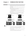
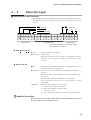
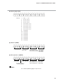
Chapter 1.
COMMUNICATION FUNCTIONS
• In the RS-485 system, up to 31 instruments can be connected with one master
station. The “instrument addresses” are then used to identify mate stations for
communication.
• The communication procedure and format are in common to the RS-232C and
RS-485 systems.
• When the following procedure is completed during communication, various
data for the instrument can be read or written.
(1) The master station (host computer) transmits an instruction message to a
slave station (instrument)
(2) The master station receives a response message from the slave station.
• Instructions from master station to slave station are classified into two types;
“read” and “write”.
• The type of ready/write data can be optionally selected by “data address”.
• CPL(Control Peripheral Link) communications network is the Yamatake
Corporation's host-communications system.
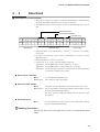
RS-485 connection example
Master station
RS-232C
RS-232C/RS-485
converter
RS-485 (5-wire system)
RS-485 connection example
Master station
RS-232C
CMC10L001A000 (*2)
RS-485 (3-wire system)
Note
• The high-performance communication controller CMC410A102 is available
for conversion between the RS-232C and RS-485 interfaces.
• When the master station is an MA500 DIM or CMC410, it can be connected to
up to 16 slave stations.
• The CMC10L001A000 communication controller is an RS-232C/RS-485 (3wire type) converter available from Yamatake Corporation.
1-1
Chapter 2.
2 - 1
WIRING
RS-485 Connection
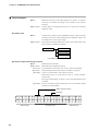
■ 5-wire RS-485 mutual connection
Terminating
resistor
DCP31/32 or
5-wire system DIGITRONIK unit
(slave station)
SDA
SDB
Terminating
resistor
RDA
RDB
SG
Shielded cable
FG
Master station
RDA
RDB
SDA
SDB
SG
FG
Shielded
cable
DCP31/32 or
5-wire system DIGITRONIK unit
(slave station)
SDA
SDB
RDA
RDB
SG
FG
Shielded cable
DCP31/32 or
5-wire system DIGITRONIK unit
(slave station)
SDA
Terminating
resistor
Terminating
resistor
SDB
RDA
RDB
SG
FG
Connect four terminating resistors of 150Ω±5%, 1/2W min. at each end of the
transmission line. Connect only one end of the shielded wire to the frame ground.
Other 3-wire system DIGITRONIK units of Yamatake Corporation can be used
on the same communication line. Conduct the wiring shown at the item "3-wire
RS-485 mutual connection" on page 2-2.
2-1
Chapter 2. WIRING
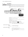
■ 3-wire RS-485 mutual connection
An example of DCP31/32 wiring with a 3-wire system unit supporting the RS485 is shown below.
DCP31/32 or
5-wire system DIGITRONIK unit
(slave station)
Terminating
resistor
SDA
SDB
*
*
RDA
RDB
SG
FG
Master station
RDA
Shielded
cable
RDB
SDA
SDB
*
*
SG
FG
Shielded
cable
3-wire system DIGITRONIK unit
(slave station)
DA
DB
SG
FG
Shielded
cable
DCP31/32 or
5-wire system DIGITRONIK unit
(slave station)
SDA
Terminating
resistor
SDB
*
*
RDA
RDB
SG
FG
Connect two terminating resistors of 150Ω±5% 1/2W min. at each end of the
transmission line. Connect only one end of the shielded cable to the FG ground.
Externally conduct the wiring for the wires marked with an asterisk.
On 3-wire system, the CMC10L001A000 of Yamatake Corporation can be used
as a converter for master station.
For the details, refer to the item "Connection with CMC10L" on page
Appendix-2.
2-2
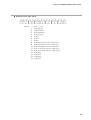
Chapter 2. WIRING
2 - 2
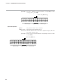
Terminal Array of DCP31/32
The terminal array of the DCP31/32 with the communication function is as
follows.
External switch
inputs
Time event outputs
T1
Load
49
57
SDA
Load
50
58
SDB
Load
51
59
RDA
Load
52
60
RDB
Load
53
61
SG
RSW5
41
RSW6
42
RSW7
43
RSW8
44
RSW9
45
RSW10
46
54
RSW11
47
55
RSW12
48
56
T2
T3
T4
T5
RS-485
communications
62
Bias circuit
63
25 To terminals
External
10 to 29 Vdc power supply
64
Handling Precautions
• Connect the shield wires to FG at one place.
• The recommended tightening torque for the terminal screws is 0.78 to
0.98 N·m.
• Maintain a distance of at least 50 cm between I/O leads or
communications lead and the power lead. Also, do not pass these leads
through the same piping or wiring duct.
• When installing the DCP31/32 in locations subject to vibration or impact,
be sure to use round crimped terminals to prevent the lead from coming
loose from the terminal.
• When wiring with crimped terminals, take care to prevent contact with
adjacent terminals.
2-3
Chapter 2. WIRING
2 - 3
Loader Jack Connection
The loader jack located on the console of DCP31/32 can be connected to a serial
communication part of personal computer by the special cable for DCP31/32.
PROG
SEG
PV
SP
OUT
TM
RUN
CYC
HLD
CH1
MAN
CH2
PRG
EV1
PROFILE
EV2
FUNC
A/M
LOADER
AT
EV3
BAT
T1
PROG
AT
OT1
T2
T3
RUN/HOLD
OT2
OT3
T4
T5
DISP
CLR
PARA
ENT
Handling Precautions
• Use the special cable for DCP31/32 in case of loader jack connection.
• Connect the special cable to a serial communication port of personal
computer.
• When connecting a ground type thermocouple to the input 2 of DCP32,
a PV value may be drifted by loader jack connection. In this case, do
not ground the personal computer. For example, exchange a 3-pole
plug for power supply for a 2-pole plug.
2-4
Chapter 3.
3 - 1
SETTING
SETUP Items of DCP31/32
Code
Item
Setting at
delivery from
factory
C84
Station address
0
C85
Transmission rate /
Character format
0
C93
CPL communications
port selection
0
Setting range
0 to 127
0:
1:
2:
3:
9600 bps/even parity, 1 stop bit
9600 bps/no parity, 2 stop bits
4800 bps/even parity, 1 stop bit
4800 bps/no parity, 2 stop bits
0: Add-on terminal
1 to 15: Loader jack (Station address)
• When set to 0, CPL communications from the loader jack is not possible. In
this case, CPL communications is possible from the add-on terminal ( 57 ,
,
,
,
) under setup C84 and C85 communications conditions.
• When set to 1 to 15, CPL communications from the loader jack is possible, and
the C93 setting becomes the station address.
Transmission rate and character format are 4800 bps, even parity and 1 stop bit.
3-1
Chapter 3. SETTING
3 - 2
Initialize
Before starting communication, initialize the communication conditions for the DCP31/32 and master station.
■ CPL communications port selection
Set one of 0 to 15 to the SETUP item C93 of the DCP31/32.
When set to 0, CPL communications is possible from the add on terminal. In this
case, set the station address and transmission rate/character format to the SETUP
items C84, C85.
When set to 1 to 15, CPL communications is possible from the loader jack. In this
case, the C93 setting becomes the station address.
Transmission rate/character format are 4800 bps, even parity and 1 stop bit.
0 is set at delivery from the factory.
■ Station address
Set a decimal number within 1 to 127 to the SETUP item C84 of the DCP31/32.
Set a different address value from the addresses of the other slave stations
connected in multi-drop on the same transmission line.
Address 0 is set as an station address at delivery from the factory. Since the
communication function is not activated at address 0, be sure to set a value other
than 0 to execute communication.
■ Transmission rate/Character format
Set one of 0 to 3 to the SETUP item C85 of the DCP31/32. At this time, set the
same transmission rate and character format as in the master station.
0: 9600 bps / even parity 1 stop bit (at delivery from the factory)
1: 9600 bps / no parity 2 stop bits
2: 4800 bps / even parity 1 stop bit
3: 4800 bps / no parity 2 stop bits
3-2
Chapter 4.
4 - 1
COMMUNICATION PROCEDURE
Outline of Communication Procedure and Messages
The outline of communication procedure, and the concept of message configuration are given in this paragraph.
■ Communication procedure
The communication procedure used is given below in simple expression
(1) The master station transmits an request message to a slave station to designate
the mate instrument for communication.
(2) The slave station processes the request message and executes read and write.
(3) Further, the slave station transmits a response message according to the
contents of processing.
(4) The master station receives the response message and executes processing.
■ Configuration of message
One message consists of two layers as shown below. This is common to the
request message from the master station and response message from a slave
station.
• Data link layer
· This layer has the basic information required for communication.
· This layer has the destination of communication message and message check
information.
• Application layer
· A layer for data read and write
· The contents change, depending upon the purpose.
The individual layers are detailed in the following items.
Many mate stations
(max. 31 instruments)
Application layer
Data link layer
Request message from master station
Response message from slave station
Slave stations
Master station
Application layer
Data link layer
The driver of the data link layer knows:
¥ Destination (station address)
¥ Load check sheet (check-sum)
The load (data) of the application layer
changes every time, depending upon the
purpose.
4-1
Chapter 4. COMMUNICATION PROCEDURE
■ Definite examples
Definitely, the messages are as shown below.
● In case of message
¥ Request message
STX
0
1
0
0
X
R
S
,
1
Data link layer
0
0
1
W
,
2
ETX
Application layer
9
A
CR
LF
Data link layer
¥ Response message
STX
0
1
0
0
X
0
0
Data link layer
,
0
,
4
2
ETX
Application layer
9
4
CR
LF
Data link layer
● In case of write request
¥ Request message
STX
0
1
0
0
X
W
S
,
1
0
Data link layer
0
1
W
Application layer
,
5
8
ETX
5
A
CR
LF
Data link layer
¥ Response message
STX
0
1
Data link layer
0
0
X
0
0
ETX
Application layer
8
2
CR
LF
Data link layer
The data link layer and application layer are detailed in and after the next
paragraph.
■ Concept of data address
This instrument uses the concept of data address to facilitate reading or writing
each intended data by addressing.
For the actual correspondence between data and address, see the "Communication
Data Table".
4-2
Data A
501W
Data B
502W
Data C
503W
:
:
Chapter 4. COMMUNICATION PROCEDURE
4 - 2
Data Link Layer
■ Description of data link layer
• The data link layer includes eight basic information for transmitting a message.
• The data link layers of an request message and response message have the same
structure.
STX
ETX
Station address
Check-sum
Sub-address
Device distinction code
CR
LF
02H 30H 41H 30H 30H 58H 52H 53H 2CH 31H 30H 30H 31H 57H 2CH 32H 03H 41H 35H 0DH 0AH
STX
0
A
0
0
X
Data link layer
R
S
,
1
0
0
1
Application layer
W
,
2
ETX
A
5
CR
LF
Data link layer
The underlined characters ( ) are always constant
when used by this instrument.
● STX (Start of TeXt)
◆ Role
: Indicates the head of a message.
❁Description · Fixed at 02H.
· When the instrument receives "STX", it is identified as the first
character of a new request message even on the course of any
message.
● Station address
◆Role
: Designates the destination instrument. Communication with one
instrument designated is permitted.
❁Description · If 0 is set as an station address, the communication function is
stopped.
Therefore to make communication be sure to set an address value
of 1 or more.
· 2 hexadecimal characters. For details, see the example.
· For the details of setting of the station address, see the
"SETTING".
❏ Example
: When the station address of the mate is 10:
(1) 10 (decimal) = 0AH (hexadecimal)
(2) When converted into character codes:
0 = 30H, A = 41H
(3) "0A" (30H, 41H) found in (2) is used as the station address.
Handling Precaution
Note that the function of the station address differs absolutely from that of
the data address of the application layer.
4-3
Chapter 4. COMMUNICATION PROCEDURE
● Sub-address
❁ Description : The sub-address is meaningless in this instrument. Be sure to set
"00" (30H, 30H) as the sub-address in the same format as in the
station address.
● Device ID code
❁ Description : The character code "X" (58H) or "x" (78H) only can be
designated in this instrument.
● ETX (End of TeXt)
◆Role
: Indicates that the application layer existed up to immediately
before.
❁ Description : Fixed at 03H.
● Check-sum
◆Role
: A value to be used to check whether or not the message has been
changed due to any error (such as noise) on the course of
communication.
❁ Description · Two hexadecimal characters
· The preparing method for the check-sum is as follows;
(1) The character codes of the message from STX to ETX are
added byte by byte.
(2) The two's complement of the result of addition is taken.
(3) The above value is converted into character codes.
❏ Example
: Description is given below, citing the example of the above
request message on the preceding page.
(1) The character codes from STX to ETX are added byte by
bytes. The one lower byte of the result of calculation is 76H.
(2) The two's complement of the result of addition is taken. the
result is 8AH.
(3) The 8AH is converted into character codes. This value is
used as the check-sum. The result is "8A"; (38H) and (41H).
For the conversion into character codes, see the example of the
station address (on the preceding page).
Handling Precaution
The check-sum in the request message can be omitted, but no check-sum
is then included in the response message. The check-sum should not be
omitted to assure the proper reception of a message.
4-4
Chapter 4. COMMUNICATION PROCEDURE
● CR and LF (Carriage Return/Line Feed)
◆Role
: Indicates the end of a message.
❁Description : "CR" is (0DH), and "LF" is (0AH).
· Be sure to use CR and LF in pair.
Handling Precautions
• If any of the following errors has occurred in the contents of the data link
layer, the instrument does not respond to them.
· The communication conditions for both stations do not meet each
other (such as different transmission speeds, or parity error
occurrence).
· The transmitted station address differs from the station address of the
object instrument.
· The station address is "00".
· STX, ETX, CR and LF are not placed at the specified positions.
· The device distinction code is neither "X" nor "x".
· The station address, sub-address, or check-sum is not two characters
long.
· The calculation result of the check-sum does not meet the check-sum
of the message.
· Non-designated characters are included in the message.
• As for the contents of the data link layer, the same message as the
request message of an instrument is set as a response message, except
for the check-sum.
• Use the upper-case characters "A" to "F" in the hexadecimal numeric
part to be used for the station address and check-sum.
4-5
Chapter 4. COMMUNICATION PROCEDURE
4 - 3
Application Layer
■ Outline of application layer
• The application layer includes an request, data, data count, and message
decision information (and code).
• The application layers of the request message and response message differ in
structure from each other.
• There are three types of request messages; "a read request", "a write request",
and "a file read request/file write request".
The response message includes a response corresponding to each request.
• It can be identified by an status code how the request message has been
processed.
Contents
Application layer
Reqeust message
Read request
Request code (RS)
Start data address
Read data count
Write request
Request code (WS)
Start data address
Write data
File read/write
request
Request code
Program No.
segment No., etc.
Block data
Response message
Read response
Status code
Read data
Write response
Status code
File read/write
response
Request code
Program No.
segment No., etc.
Block data
4-6
Chapter 4. COMMUNICATION PROCEDURE
4 - 4
Data Read
■ Description of read request
• This request permits the contents of continuous data addresses starting with the
read start data address designated to be read in one message.
• The application layer of a read request consists of the following three types of
data:
Read request code
Read start data adddress
Read data count
02H 30H 31H 30H 30H 58H 52H 53H 2CH 31H 30H 30H 31H 57H 2CH 32H 03H 39H 41H 0DH 0AH
STX
0
A
0
0
X
Data link layer
R
S
,
1
0
0
1
W
,
2
Application layer
ETX
9
A
CR
LF
Data link layer
• Individual data are partitioned by a comma "," (character code 2CH),
respectively.
• An upper-case character code is used for each numeric or character in the
application layer.
• Decimal number is used for each numeric.
• Unnecessary "0" or a space cannot be added to each data.
❏ Example : The underlined part of "RS, 01001W, 2" is wrong.
❏ Example : The underlined parts of "RS, 1001W, 02" are wrong.
❏ Example : The above figure indicates an example that two-data information
is read from 1001W in one message.
● Read request code (RS)
◆Role
: A command which indicates read.
❁Description : Two characters "RS" (52H, 53H).
● Read start data address
◆Role
: Designates the start data address from which data is to be read.
❁Description : The correspondence between data address and read data is shown
in the "Communication Data Table".
· Be sure to add "W" (75H) immediately after the numeric of the
data address.
● Read data count
◆Role
: It is designated how many data are read continuously, starting
with the designated data address.
Handling Precaution
For the high limit of the read data count, see the "Communication Data
Table".
4-7
Chapter 4. COMMUNICATION PROCEDURE
■ Read response
◆Role
: When the message in the data link layer is proper, a response
message is sent back according to the contents of the request
message.
❁Description : All the data in the application layer are expressed in decimal
character codes.
● Status code
◆Role
: A numeric by which it can be identified how the request message
has been processed on the instrument side. Different value is set
according to the result of processing.
❁Description : The response message includes an "status code" without fail. The
status codes are classified as follows;
* Status code
Normal
Warning
Error
* The status code is two decimal digits.
● Normal response/warning response
◆Role
: Sends back the read data.
❁Description : Information in the application layer
· Status code : For the details of the status code, see the "Status code Table".
· Read data : The decimal point is removed from a numeric to be put in.
❏ Example : "55.6" is converted into "556" when it is put in.
: Individual data are partitioned with a comma (2CH),
respectively.
: The range and number of digits of each data depend upon the
read data.
❏ Example : In case of normal response (when there are two read data, and all
the data are read properly)
Status code (00=normal)
Read data
02H 30H 31H 30H 30H 58H 30H 30H 2CH 31H 32H 33H 2CH 38H 37H 30H 03H 46H 35H 0DH 0AH
STX
0
1
0
Data link layer
4-8
0
X
0
0
,
1
2
3
,
Application layer
8
7
0
ETX
F
5
CR
Data link layer
LF
Chapter 4. COMMUNICATION PROCEDURE
❏ Example : In case of warning response (numeric corresponding to the
warning code is put in ✽ ✽.)
Status code (✽✽=warning)
Read data
02H 30H 31H 30H 30H 58H ✽H ✽H 2CH 30H 2CH 38H 37H 30H 03H ??H ??H 0DH 0AH
STX
0
1
0
0
X
✽
✽
Data link layer
,
0
,
8
7
Application layer
0
ETX
?
?
CR
LF
Data link layer
● Error response
◆Role
: Indicates that there is an error in the request message, and it
cannot be normally read. Therefore, there is no data herein.
❁Description : Information in the application layer.
· Status code : Indicates an error type.
For details, see the "Status code Table".
❏ Example : In case of error response:
Status code (✽✽=error)
02H 30H 31H 30H 30H 58H ✽H ✽H 03H ??H ??H 0DH 0AH
STX
0
1
0
Data link layer
0
X
✽
✽
ETX
Application layer
?
?
CR
LF
Data link layer
■ Expression of decimal numeric (numeric data)
◆Role
: All the numeric part, read count, write value (described in WS
command), and read data at the data address follow the rules
given below.
(1) When a numeric is negative, add a minus sign "–" (2DH) before the
numeric.
❏ Example: "-123" (2DH, 31H, 32H, 33H)
(2) When a numeric is 0, use one 0.
❏ Example: "0" (30H)
❏ Example: "00" (30H, 30H) is wrong.
(3) When a numeric is positive, never add a plus sign "≠" before the numeric.
❏ Example: "+123"+ (2BH, 31H, 32H 33H) is wrong.
(4) Never add unnecessary 0 or a space before a numeric.
❏ Example: "0123" (30H, 31H, 32H, 33H) is wrong.
❏ Example: "123" (20H, 31H, 32H, 33H)
4-9
Chapter 4. COMMUNICATION PROCEDURE
4 - 5
Data Write
■ Description of write request
• This request permits the contents of continuous data addresses, starting with the
designated write start data address to be simultaneously written in one message.
• The application layer of a write request consists of the following three types of
data:
Write request code
Wirte data (1st data)
Write start data address
Write data (2nd data)
02H 30H 31H 30H 30H 58H 57H 53H 2CH 30H 30H 30H 31H 57H 2CH 32H 2CH 36H 35H
STX
0
1
0
0
X
Data link layer
W
S
,
1
0
0
1
W
,
2
,
6
5
Application layer
03H 46H 45H 0DH 0AH
ETX
F
E
CR
LF
Data link layer
• Individual data are partitioned with a comma "," (character code 2CH),
respectively.
• The write data count need not be designated.
• An upper case character code is used for each numeric or character in the
application layer.
• Decimal number is used for each numeric.
• Unnecessary "0" (30H) or a space cannot be added to each data.
❏ Example : The underlined part of "WS, 01001W, 2" is wrong.
❏ Example : The underlined parts of "WS, 1001W, 02" are wrong.
❏ Example : The above figure shows an example that 2 and 65 are written at
addresses 1001W and 1002W, respectively, in one message.
● Write request code (WS)
◆Role
: A command which indicates write.
❁Description : Two characters "WS" (57H, 53H)
● Write start data address
◆Role
4-10
: Designates the start data address for write.
· For the correspondence between the data address and write data,
see the "Communication Data Table".
· Be sure to add "W" (57H) after the numeric representing the data
address.
Chapter 4. COMMUNICATION PROCEDURE
● Write data
◆Role
: Data to be written at continuous addresses starting with the
designated data address.
❁Description : The range of a numeric to be written differs, depending upon
each data address.
· Individual data are partitioned with a comma (2CH),
respectively.
· The data address at which the corresponding data is written is
incremented by 1 sequentially, starting with the start data address
(see the example given on the preceding page).
· The number of data which can be written in one message is
limited. For details, see the "Communication Data Table".
■ Write response
◆Role
: When the message in the data link layer is proper, the status code
only is sent back.
❁Description : The status codes are classified as follows;
* Status code
Normal
Warning
Error
* The status code is expressed in two decimal digits.
● Normal response/warning response
◆Role
: Information concerning the result of processing the write request
message is sent back.
Only the normal status code or warning status code is sent back.
❁Description : Information in the application layer
· Status code : A numeric by which it can be identified how the request message
has been processed on the instrument side.
❏ Example : An example of normal response (when all data are properly
written)
Status code (00=normal)
02H 30H 31H 30H 30H 58H 30H 30H 03H 38H 32H 0DH 0AH
STX
0
1
0
Data link layer
0
X
0
0
ETX
Application layer
8
2
CR
LF
Data link layer
4-11
Chapter 4. COMMUNICATION PROCEDURE
❏ Example : In case of warning response (numeric corresponding to the
warning code is put in ✽ ✽).
Status code (✽✽=warning)
02H 30H 31H 30H 30H 58H ??H ??H 03H ??H ??H 0DH 0AH
STX
0
1
0
0
Data link layer
X
✽
✽
ETX
Application layer
?
?
CR
LF
Data link layer
● Error response
◆Role
: Only the error status code is sent back.
❁Description : Information in the application layer
· Status code : Indicates that there is an error in the request message, and write
processing cannot be done.
❏ Example : In case of error response (numeric corresponding to the error code
is put in ✽ ✽).
Status code (✽✽=Error)
02H 30H 31H 30H 30H 58H ✽H ✽H 03H ??H ??H 0DH 0AH
STX
0
1
0
Data link layer
4-12
0
X
✽
✽
ETX
Application layer
?
?
CR
Data link layer
LF
Chapter 4. COMMUNICATION PROCEDURE
4 - 6
File READ/WRITE (program pattern)
Description is given below on the program pattern, citing an example of request/response.
In this example, it is assumed that the slave station address is 01, and there is no check-sum.
The program pattern can be processed by the file operation of the CPL communications.
More than one file cannot be opened simultaneously.
The file operations of the DCP31/32 are classified into the following types:
1. File OPEN
2. File CLOSE
3. File Block READ
4. File Block WRITE
5. File DELETE
Flow example of file read
(Segments 1, 2 and 3 of
program No. 1 are read.)
Flow example of file write
In case of new preparation
(Segments 1, 2 and 3 of
program No. 1 are written.)
Flow example of file write
In case of rewrite
(Segments 1, 2 and 3 of
program No. 1 are written.)
File 01 OPEN (READ)
File 01 OPEN (WRITE)
File 01 OPEN (WRITE)
File READ (segment 1)
File WRITE (segment 1)
File WRITE (segment 1)
File READ (segment 2)
File WRITE (segment 2)
File WRITE (segment 2)
File READ (segment 3)
File WRITE (segment 3)
File WRITE (segment 3)
File CLOSE
File CLOSE
File CLOSE
(File DELETE can be used independently.)
Handling Precautions
•When an operator operates a program pattern from the console, the
OPEN request causes an error end.
•An operator can't make a program pattern operation from the console
during file OPEN.
4-13
Chapter 4. COMMUNICATION PROCEDURE
■ File OPEN
● OPEN request (FO command)
Request code
Attribute
R: READ only enable
W: WRITE only enable
Program No.
(file ID)
STX
0
1
0
0
X
F
O
,
Data link layer
1
5
,
Block count (fixed at 0)
R
,
0 ETX CR
Application layer
LF
Data link layer
● Normal response
Status code (2 decimal digits)
Program No. (File ID)
File OPEN
STX
0
1
0
0
X
0
0
Data link layer
,
F
O
,
Application layer
1
5
ETX CR
LF
Data link layer
● Error response
Error status code
STX
0
1
0
Data link layer
0
X
9
9
ETX CR
LF
Application layer Data link layer
• When set to 1 to the variable parameter settings PrtC, an OPEN request setting
W for the attribute causes an error end.
Handling Precaution
If the next command is transmitted within 10s after the file is opened, the
OPEN status continues. However, the time elapses for 10s without
transmitting the command, the file is automatically closed.
4-14
Chapter 4. COMMUNICATION PROCEDURE
■ File CLOSE
● CLOSE request (FC command)
Request code
Program No. (File ID)
STX
0
1
0
0
X
F
Data link layer
C
,
1
5
Application layer
ETX CR
LF
Data link layer
● Normal response
Status code (2 decimal digits)
Program No. (File ID)
File CLOSE
STX
0
1
0
0
X
0
0
Data link layer
,
F
C
,
Application layer
1
5
ETX CR
LF
Data link layer
● Error response
Error status code
STX
0
1
0
Data link layer
0
X
9
9
ETX CR
LF
Application layer Data link layer
4-15
Chapter 4. COMMUNICATION PROCEDURE
■ File block READ
● Block READ request (FR command)
Request code
Program No. (File ID)
Segment No. (Block No.)
STX
0
1
0
0
X
F
R
Data link layer
,
1
5
,
1 ETX CR
Application layer
LF
Data link layer
● Normal response
Program No. (File ID)
Status code
(2 decimal digits)
Segment No. (Block No.)
Request code
STX
0
1
0
0
X
0
0
,
F
R
Data link layer
,
1
Block data
(ASCII code)
5
,
1
,
Application layer
ETX CR
LF
Data link layer
● Error response (1)
Error status code
(2 decimal digits)
See the "Status Code Table".
Program No. (File ID)
Request code
STX
0
1
0
0
X
5
1
Data link layer
,
F
R
,
Application layer
● Error response (2)
Error status code
STX
0
1
0
Data link layer
4-16
1
0
X
9
9
ETX CR
LF
Application layer Data link layer
Segment No. (Block No.)
5
,
1
ETX CR LF
Data link layer
Chapter 4. COMMUNICATION PROCEDURE
■ File block WRITE
● Block WRITE request (FW command)
Program No. (File ID)
Segment No. (Block No.)
Request
code
STX
0
1
0
0
X
F
W
,
Block data (ASCII code)
1
Data link layer
5
,
1
ETX CR
Application layer
LF
Data link layer
● Normal response
Error status code
(2 decimal digits)
Program No. (File ID)
Request code
STX
0
1
0
0
X
0
0
,
Data link layer
F
W
,
1
Segment No. (Block No.)
5
,
1
Application layer
ETX CR LF
Data link layer
● Error response (1)
Error status code
(2 decimal digits)
See the "Status Code Table".
Program No. (File ID)
Request Code
STX
0
1
0
0
X
5
1
Data link layer
,
F
W
,
1
Application layer
Segment No. (Block No.)
5
,
1
ETX CR LF
Data link layer
● Error response (2)
Error status code
STX
0
1
0
Data link layer
0
X
9
9
ETX CR
LF
Application layer Data link layer
• When set to 1 to the variable parameter settings PrtC, a Block WRITE request
causes an error end.
4-17
Chapter 4. COMMUNICATION PROCEDURE
■ File DELETE (deletion)
● File DELETE request (FD command)
Request code
Program No. (File ID)
STX
0
1
0
0
X
F
Data link layer
D
,
1
5 ETX CR
Application layer
LF
Data link layer
● Normal response (indicates that the deletion operation ends)
Status code (2 decimal digits)
Request code
Program No. (File ID)
STX
0
1
0
0
X
0
0
Data link layer
,
F
D
,
Application layer
1
5 ETX CR
LF
Data link layer
● Error response
Error status code 50 : File is OPEN
99 : Undefined command
STX
0
1
0
0
X
9
9
ETX CR
LF
Application layer Data link layer
Data link layer
•
•
•
•
•
Execute the file DELETE in a CLOSE status.
It takes 0.2s max. to delete a file.
After the file DELETE is completed, the normal response is sent back.
When a file has been already deleted, the normal response is sent back.
The program being run currently cannot be deleted (except for the constant
value mode).
• When set to 1 to the variable parameter settings PrtC, a File DELETE request
causes an error end.
4-18
Chapter 4. COMMUNICATION PROCEDURE
4 - 7
Run Operation
The run operation is executed by the bit write request or write request.
In the run operation, more than one write operation are ineffective, and only the extreme LSB side operation is
processed effectively. The run operation cannot also be executed over two or more words.
● Bit write request (WB command)
Only the bit write of the run operation is effective under the WB command.
Request code
Bit position
Write address
Bit data
RUN
command
STX
0
1
0
0
X
W
B
,
Data link layer
5
0
8
,
1
,
1
Application layer
ETX CR
LF
Data link layer
or
STX
0
1
0
0
X
W
B
,
5
Request code
Bit position
Write address
Bit data
0
Data link layer
8
.
0
,
0
1
0
0
Application layer
RUN
command
ETX CR
LF
Data link layer
● Write request (WS command)
Request code
Data group
Write start address
STX
0
1
0
0
X
W
S
,
5
0
Data link layer
8
W
,
2
,
1
,
5
5
Application layer
ETX CR
LF
Data link layer
● Normal response
Status code 00 : Normal
STX
0
1
0
Data link layer
0
X
0
0
ETX CR
LF
Application layer Data link layer
4-19
Chapter 4. COMMUNICATION PROCEDURE
● Error response
STX
0
1
0
Data link layer
0
X
9
9
Error status code 99 : Start address error, word count error,
undefined command
10 : Meaningless setting, ineffective setting
XX : White data error
ETX CR LF
Application layer Data link layer
Handling Precautions
•It takes 0.2s max. before the RUN mode starts after the DCP31/32
receives the RUN command in the READY status and sends back a
normal response. This time changes, depending upon the internal
processing status of the DCP31/32.
Status 1 to MV can be obtained by reading the same address. (See Chapter 5
"Communication Data Table".)
Address
Data item
Data (decimal)
Read data
508W
Run operation 1
Status 1
509W
Run start segment No.
1 to 30
Segment No.
510W
Run start program No.
1 to 19
Program No.
511W
Manual MV1
–100 to +1100
MV1
512W
Manual MV2
–100 to +1100
MV2
The 1st word is a request flag of 16 bits. The run operation can be done by writing
at this address. This is achieved by the usual write request or bit write request.
The run operation can be checked by reading the status 1.
A response is sent back after checking if the run operation is accepted, and the
time required for it is 100 to 200ms.
When the segment No. data and program No. data corresponding to the 2nd and
3rd words, respectively, are designated independently in the READY status, the
run start program No. and run start segment No. are changed.
These data indicated on the LED indicators on the console are then also changed.
These data may be used in combination with RUN or advance request.
The function in such cases are shown on the table given on the next page.
In any other cases, these data are ignored.
The data in and after the 4th word are ignored.
When only the program No. is designated, the segment is set to 1.
As for the MV1 of the 4th word, MV in the MANUAL mode on CH1 side should
be designated or it should be used in combination with MANUAL request.
In any other cases, this data is ignored.
The data in and after the 5th word are also ignored.
As for the MV2 of the 5th word, MV in the MANUAL mode on CH2 side should
be designated. In any other cases, this data is ignored.
4-20
Chapter 4. COMMUNICATION PROCEDURE
■ Run operation bit definition (command)
● Run operation 1
MSB
2
15
16
LSB
2
14
15
2
13
14
2
12
13
Write disable
2
11
12
2
10
11
2
9
10
2
9
0001:FAST start
When 1, ADV (bit write disable)
8
7
2
8
7
2
6
2
5
6
2
4
5
2
3
4
0001: AUTO (CH1)
0010: MANUAL (CH1)
0100: AT start (CH1)
1000: Undefined
2
2
3
1
20
2
1
2
0001: RESET
0010: RUN
0100: HOLD
1000: Undefined
However, this is operated when the D1 input is turned OFF since the D1 input has
priority.
Run
operation
SEG No.
PRG No.
MAN MV
Operation of DCP31/32
RESET
Ignore
Ignore
Ignore
READY status is set.
RUN
(Note 1)
Necessary
necessary
Ignore
In READY status, RUN starts with PRG No. and
SEG No. given to the left.
None
None
None
In READY status, RUN starts with PRG No. and
SEG No. already selected.
RUN
Ignore
Ignore
Ignore
In HOLD or FAST status, RUN starts.
HOLD
Ignore
Ignore
Ignore
In RUN or FAST status, HOLD is set.
ADV
(Note 3)
Necessary
None
None
In RUN, HOLD or FAST status, SEG No. given to
the left becomes a start point.
Necessary
Necessary
Ignore
In RUN, HOLD or FAST status, PROG No. and
SEG No. given to the left become a start point.
Ignore
Ignore
None
In AUTO on CH1 side status, it is changed over to
MANUAL status.
Ignore
Ignore
None
In AUTO on CH1 side status, it is changed over to
MANUAL status, and MV given to the left is set.
In MANUAL status, MV given to the left is set.
During AT execution, AT is interrupted.
AUTO
(CH1)
Ignore
Ignore
Ignore
In MANUAL on CH1 side status, it is changed over
to AUTO status.
During AT execution, AT is interrupted.
FAST
Ignore
Ignore
Ignore
In RUN or HOLD status, FAST starts.
AT START
Ignore
Ignore
Ignore
AT starts. (Note 2)
MANUAL
(CH1)
Note 1) (1) When PRG No and SEG No. are not set to the program, the READY
status cannot be changed over to RUN.
(2) The READY status cannot be changed over to RUN during key
operation.
Note 2) When the following conditions are all satisfied, AT starts on CH1 side.
(1) Controller function is set on CH1 side.
(2) Output is not heat/cool type on CH1 side.
(3) One of RUN, HOLD, FAST or END status is set.
(4) AUTO mode is selected on CH1 side.
(5) 0 is not set to the variable parameter setting At.
Note 3) ADV is accepted only as shown in the following examples.
WS, 508W, 4096, 20 (ADV to segment 20).
WS, 508W, 4096, 20, 2 (ADV to segment 20 of program 2).
4-21
Chapter 4. COMMUNICATION PROCEDURE
● Run operation 2
MSB
2
15
LSB
2
16
14
15
2
13
2
14
12
13
2
11
12
Write disable
2
10
11
2
9
10
2
8
9
2
7
8
Write disable
2
6
7
2
5
6
2
4
5
2
3
4
Write disable
2
2
3
1
20
2
1
2
Write disable
Data cannot be written for the DCP31.
Though write data is disable for the DCP32, plural data can be written to the MV2
(512W) to the Run operation (3) simultaneously because data can be written to the
Run operation (2).
● Run operation 3
MSB
2
15
16
LSB
2
14
15
2
13
14
2
12
13
Write disable
2
11
12
2
10
11
2
9
10
Write disable
2
8
9
7
2
8
7
2
6
2
5
6
2
4
5
2
3
4
2
2
3
20
2
1
2
Write disable
0001: AUTO (CH2)
0010: MANUAL (CH2)
0100: AT start (CH2)
1000: Undefined
Data cannot be written for the DCP31.
When the following conditions are all satisfied, AT starts on CH2 side.
(1) Controller function is set on CH1 side.
(2) Output is not heat/cool type on CH2 side.
(3) One of RUN, HOLD, FAST, END status is set.
(4) Auto mode is selected on CH2 side.
(5) 0 is not set to the variable parameter 2 setting At.2.
4-22
1
Chapter 4. COMMUNICATION PROCEDURE
4 - 8
Status Code Table
■ Normal and error ends
Status code
Type
Name
Contents.
00
Normal
Command normal
Request message is ended normally
01
Normal
Command normal
Request message is ended normally regarding the
last block.
40
Error
Former error
Request message is in error.
41
Error
Data number error
The number of data is over 16.
(Including read data count of RS request)
42
Error
Data address error
The data address is not defined.
All of message has been cancelled.
43
Error
Data error
The value of write data is in error.
All of message has been cancelled.
44
Error
Data limit error
The value of write data is out of the limit.
Processing is continued except for the relevant data
address.
45
Error
Write error
The data cannot be written according to the status of
DCP31/32.
(Settings can be changed only READY mode
regarding all of setup items and some of event
configuration data)
Write is attempted to the write inhibit data address.
47
Error
Impossible mode change
Mode can not be changed.
48
Error
Console operating
Operation keys of console are operated by an
operator.
Send the request message after key operation.
50
Error
Double open
File is already open.
51
Error
File closed
File is not open yet.
52
Error
Program number/
Segment number error
Program number or segment number is in error.
No program in the segment.
54
Error
Read/Write violation
Attribute of File OPEN is violated.
57
Error
Block data error
Block data of File block WRITE is in error.
58
Error
Running program delete
The program being run cannot be deleted.
59
Error
Program protect
File OPEN, File block WRITE and File DELETE are
inhibited.
99
Error
Command error
The command is undefined.
4-23
Chapter 4. COMMUNICATION PROCEDURE
4 - 9
Timing Specifications
■ Timing specifications for request message and response message
When a slave station is connected with the master station directly, the following
precautions should be observed concerning the transmit timings of an request
message from the master station and a response message from the slave station.
● Response monitor time
The maximum response time required from the end of transmitting an request
message from the master station to the start of receiving a response message from
the salve station is 2s (section (1)). Therefore, the response monitor time should
be set to 2s.
Generally, when the response monitor time reaches time up, the request message is
retransmitted.
For details, see the "Communication Program for Master station".
● Transmit start time
A wait time of 10ms or more is required before the master station starts to transmit
the next request message (to the same slave station or a different slave station)
after the end of receiving a response message (section (2)).
●
RS-485 3-lead sytem
Transmission
line
●
Request
message
RS-485 5-lead sytem
Master station,
transmission line
Slave station,
transmission line
(2)
(1)
Request
message
Resopnse
message
Resopnse
message
(2)
(1)
Request
message
Request
message
Resopnse
message
Resopnse
message
(1) End of master station transmit — Request interval time of slave station = 2000ms max
(2) End of slave station transmit — Request interval time of master station = 10ms min.
4-24
Chapter 4. COMMUNICATION PROCEDURE
■ RS-485 driver control timing specification
When the transmit/receive of the RS-485 3-lead system is directly controlled by
the master station, utmost care should be exercised about the following timing.
(1)
Master station
Driver control
(Enable)
(Disable)
Effective
data
(Request
message)
Transmission line
Slave station
Driver control
(4)
(Disable)
Effective
data
(Response
message)
(Enalbe)
(2)
End of master station
transmit
(3)
End of slave station
transmit
(1) Transmit end of master station — Driver disable time = 500 s max.
(2) Receive end of slave station — Drive enable time = 1ms min.
(3) Transmit end of slave station — Drive disable time = 10ms max.
(4) Receive end of aster station — Drive enalbe time = 10ms max.
4-25
Chapter 5.
5 - 1
COMMUNICATION DATA TABLE
Preliminary Knowledge of Communication Data Handling
■ Types and formats of communication data
● Types of communication data
The communication data are classified into the following types:
• Run status
: Data indicating the run status of the DCP31/32 (PV,
alarm, etc.)
• Variable parameter : Data to be changed during running.
• Variable parameter 2 : Data to be changed during running for CH2.
• Event configuration data
: Data for setting an event type and other event outputs.
• PID parameter
: Data for setting PID constants, output limiter, etc. for
CH1.
• PID parameter 2
: Data for setting PID constants, output limiter, etc. for
CH2.
• Setup data
: Data for setting the status of the DCP31/32 before
running. (setting of input range, etc.)
• Table data
: Data for setting input linearization table approximation.
• Constant-value operation data
: Data for setting SP, PID constants, etc. to be used in the
constant value control mode.
• Program pattern (block data)
: Data for setting the run pattern such as SP, and TIME.
These data are communication every data type.
● Format of communication data
The communication data are classified into the following formats:
• Numeric data
: Data indicating numerics (PV, SP, etc.)
• Bit data
: Data, each bit of which is given meaning (alarm, etc.).
The bit data must be composed during transmit, and be
decomposed during receive.
■ Data address
The data addresses are allocated as shown in the table below.
Communication data
Offset
Address
DCP31
Address
DCP32
Run status
500
501 to 526
501 to 526
Variable parameter
2500
2501 to 2533
2501 to 2533
Variable parameter 2
3000
—
3001 to 3022
Event configuration data
3500
3501 to 3513
3501 to 3513
PID parameter
1500
1501 to 1580
1501 to 1580
PID parameter 2
2000
—
2001 to 2080
Setup data
4500
4501 to 4600
4501 to 4600
Table data
4000
4001 to 4022
4001 to 4044
Constant-value operation data
1000
1001 to 1026
1001 to 1046
5-1
Chapter 5. COMMUNICATION DATA TABLE
■ Data read/write count
The data count which can be continuously read/written by once communication is
predetermined as shown in the table below.
Category
Data count
Read
1 to 16
Write
1 to 16
Among the continuous data, any data which do not exist due to difference in
model number are handled as shown below.
• Read
: 0 is read as a dummy data (warning end).
• Write
: Not written (warning end).
■ Data unit and decimal point position
A decimal point is not added to read/write data.
The unit or decimal point position is predetermined every data.
For the unit and decimal point position of each data, see the request manual for the
main unit of instrument.
Example: When data to be read/written is numeric value 105, its unit or decimal
point position is automatically determined by the data address, the
SETUP item of the instrument and the others.
Therefore, the numeric data 105 is expressed as 10.5%, 105˚C, or the
like according to the data address of data to be read/written.
5-2
Chapter 5. COMMUNICATION DATA TABLE
■ Notes
• Cautions on instrument console display
When data is written by communication with respect to a parameter indicated in
the input ready status of the instrument, the display is not changed into the
value set by communication, but the preceding value is kept as it is. This is
because the display data to LED is not updated irrespective of change in the
internal data. When the currently indicated parameter is transferred once to
another parameter, and it is recalled, the value changed by communication is
indicated correctly.
When the instrument is placed in the basic display status (SP/PV/MV display
status), the display is always updated according to the internal data. Therefore,
even when an SP is rewritten by communication, the changed value is indicated
immediately.
• Keylock
Even when the instrument is set to the keylock status, data can be written by
communication.
• Restrictions on read
Any parameters which cannot be called by key operation on the instrument can
be all called by communication.
If an address out of the range (non-designated address) is accessed, the end
code "42" is returned.
• Restrictions on write
Any parameters which cannot be input by key operation on the instrument can
be written by communication. The restrictions on write (the high and low
limits, etc.) are the same as in the usual input by a console.
Even a parameter which can be input by key operation may not be able to be set
by communication under an inapropriate condition.
• In case more than one data including error data are to be written in once
message.
For example, assume that the proportional band, integral time, and derivative
time are written like WS, 1501W, 300, 6001, 20. Since I then exceeds the
effective range, the response "44" (error response) is returned.
At this time, beware of the following points:
(1) Data is written until a set disable data appears.
(2) No data is written at a word address where a set disable data exists, but the next
data is processed.
In the case of this example, therefore 300 and 20 are written normally, but 6001 is
not written, and the value before the message is received remains.
• Status write
The status write command makes the LSB side of bit information effective.
For example, when WS, 508W, 3 (both AUTO and MANUAL are designated)
is written, this is interpreted as AUTO command, and MANUAL is ignored.
5-3
Chapter 5. COMMUNICATION DATA TABLE
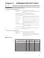
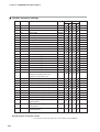
5 - 2
Communication Data Table
The address and read/write (R/W) enable status of each data are determined as shown in the table below.
● Meaning of symbols in R/W column
R : READ
W : WRITE
❍ : Enable
× : Disable
▲ : Enable, however, fixed value depending upon the instrument
❏ : Enable, however, a blank area
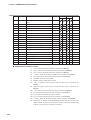
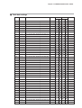
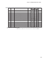
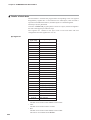
■ Run status
No.
Format
Item
Address
DCP31
DCP32
R
W
R
W
501W
❍
×
❍
×
Remarks
1
Bit
Alarm status (1)
2
Bit
Alarm status (2)
502W
❍
×
❍
×
3
Bit
Event output status
503W
❍
×
❍
×
4
Numeric
PV1
504W
❍
×
❍
×
5
Numeric
SP1
505W
❍
❍
❍
❍
6
Numeric
PV2
506W
❏
×
❍
×
7
Numeric
SP2
507W
❏
×
❍
❍
*2
8
Bit
Status (1)/Run operation (1)
508W
❍
❍
❍
❍
*3
*1
9
Numeric
Segment No.
509W
❍
❍
❍
❍
*4
10
Numeric
Program No.
510W
❍
❍
❍
❍
*4
11
Numeric
MV1
511W
❍
❍
❍
❍
*5
12
Numeric
MV2
512W
❏
×
❍
❍
*6
13
Bit
Status (2)/Run operation (2)
513W
❍
×
❍
❍
14
Bit
Status (3)/Run operation (3)
514W
❏
×
❍
❍
15
Numeric
Segment progress time
515W
❍
×
❍
×
*7
16
Numeric
Run progress time
516W
❍
×
❍
×
*7
17
Numeric
Using PID group No. (CH1)
517W
●
×
●
×
*8
18
Numeric
Using PID group No. (CH2)
518W
❏
×
❍
×
*9
19
Numeric
Cycle execution count
519W
❍
×
❍
×
*10
20
Numeric
PVd
520W
❏
×
❍
×
21
Numeric
PVw
521W
❏
×
❍
×
22
Numeric
SPw
522W
❏
×
❍
❍
23
Numeric
Heat MV
523W
❍
×
❍
×
*11
24
Numeric
Cool MV
524W
❍
×
❍
×
*11
25
Numeric
Motor feedback value
525W
❍
×
❍
×
*12
26
Bit
External switch input status
526W
❍
×
❍
×
● Explanation of remarks column
*1 WRITE is enable when the programmer function is set, and MANUAL mode
is selected on the side of CH1.
*2 WRITE is enable when the programmer function is set, and MANUAL mode
is selected on the side CH2.
*3 The data functions as the item of status (1) in case of READ. The data
functions as the item of run operation 1 in case of WRITE. Bit assignment is
different between status (1) and run operation (1).
5-4
Chapter 5. COMMUNICATION DATA TABLE
*4
WRITE is enable in READY mode. WRITE is enable when RUN operation
is done in READY mode. WRITE is enable when the ADV operation is
done.
*5 –100 to +1100 can be written when the programmer function is set, and the
MANUAL mode is selected on the side of CH1.
*6 –100 to +1100 can be written when the programmer function is set, and the
MANUAL mode is selected on the side of CH2.
*7 0 to 5999 minute can be read when set to 0 for the set up item C64 (program
time unit). 0 to 5999s can be read when set to 1.
*8 1 to 8 can be read except for the heat/cool output on the side of CH1.
*9 1 to 8 can be read except for the heat/cool output on the side of CH2. 1 to 4
can be read in case of the heat/cool output on the side of CH2.
*10 0 to 9999 can be read.
*11 –100 to +1100 can be read in case of the heat/cool output.
*12 –500 to +1500 can be read in case of the position proportion output (2G).
5-5
Chapter 5. COMMUNICATION DATA TABLE
● Alarm status 1
215
214
213
212
211
210
29
28
27
26
25
24
23
22
21
20
16
15
14
13
12
11
10
9
8
7
6
5
4
3
2
1
Each bit
0
1
2
3
4
5
6
7
8
9
10
11
12
13
14
15
16
: OFF, 1 : ON
: AL01 Input 1 over-range
: AL02 Input 1 under-range
: AL03 Input 2 over-range [DCP32 only]
: AL04 Input 2 under-range [DCP32 only]
: Undefined
: Undefined
: AL07 Input 1 RTD disconnection A
: AL08 Input 1 RTD disconnection B
: AL09 Input 1 RTD disconnection C
: AL10 MFB disconnection
: AL11 MFB short-circuit
: AL12 MFB adjustment impossible
: AL13 Input 2 RTD disconnection A [DCP32 only]
: AL14 Input 2 RTD disconnection B [DCP32 only]
: AL15 Input 2 RTD disconnection C [DCP32 only]
: AL16 Humidity calculation error [DCP32 only]
● Alarm status 2
215
214
213
212
211
210
29
28
27
26
25
24
23
22
21
20
16
15
14
13
12
11
10
9
8
7
6
5
4
3
2
1
Each bit
5-6
0
1
2
3
4
5
6
7
8
9
10
11
12
13
14
15
16
: OFF, 1 : ON
: AL70 A/DT malfunction
: AL71 A/D2 malfunction [DCP32 only]
: Undefined
: Undefined
: Undefined
: Low battery voltage
: Undefined
: AL81 Board configuration error
: Undefined
: AL83 Input 2 Cold junction compensation impossible
: Undefined
: Undefined
: AL96 Program error
: AL97 Parameter error
: AL98 Adjustment value error
: AL99 PROM error
Chapter 5. COMMUNICATION DATA TABLE
● Event output status
215
214
213
212
211
210
29
28
27
26
25
24
23
22
21
20
16
15
14
13
12
11
10
9
8
7
6
5
4
3
2
1
Each bit
0
1
2
3
4
5
6
7
8
9
10
11
12
13
14
15
16
: OFF, 1 : ON
: Event 1 (EV1)
: Event 2 (EV2)
: Event 3 (EV3)
: Time event 1 (T1)
: Time event 2 (T2)
: Time event 3 (T3)
: Time event 4 (T4)
: Time event 5 (T5)
: Undefined
: Undefined
: Undefined
: Undefined
: Undefined
: Undefined
: Undefined
: Undefined
● Status 1 (READ)
215
214
213
212
211
210
29
28
27
26
25
24
23
22
21
20
16
15
14
13
12
11
10
9
8
7
6
5
4
3
2
1
Undefined (fixed at 0) 0000: FAST stop
0001: FAST
0001: AUTO (CH1)
0000: END
0010: MANUAL (CH1) 0001: READY
0100: During AT (CH1) 0010: RUN
0100: HOLD
● Run operation 1 (WRITE)
215
214
213
212
211
210
29
28
27
26
25
24
23
22
21
20
16
15
14
13
12
11
10
9
8
7
6
5
4
3
2
1
Write disable
0001: FAST start
ADV when going to 1
(bit write disabled)
0001: AUTO (CH1)
0001: RESET
0010: MANUAL (CH1) 0010: RUN
0100: AT start (CH1) 0100: HOLD
Note
See 4-7 Run operation (page 4-19) for details.
5-7
Chapter 5. COMMUNICATION DATA TABLE
● Status 2 (READ)
215
214
213
212
211
210
29
28
27
26
25
24
23
22
21
20
16
15
14
13
12
11
10
9
8
7
6
5
4
3
2
1
0000: ST standby
stop
0001: During ST
(CH1)
Undefined
(fixed at 0)
0000: Without GS
standby (CH1)
0001: GS standby
(CH1)
0001: Program
0010: Constant-value
operation
● Run operation 2 (WRITE)
215
214
213
212
211
210
29
28
27
26
25
24
23
22
21
20
16
15
14
13
12
11
10
9
8
7
6
5
4
3
2
1
Write disable
Write disable
Write disable
Write disable
Note
See 4-7 Run operation (page 4-19) for details.
● Status 3 (READ)
215
214
213
212
211
210
29
28
27
26
25
24
23
22
21
20
16
15
14
13
12
11
10
9
8
7
6
5
4
3
2
1
0001: AUTO (CH2)
Undefined
0000: ST standby
0000: Without GS
stop (CH2)
standby (CH2) 0010: MANUAL (CH2) (fixed at 0)
0001: During ST (CH2) 0001: GS standby 0100: During AT (CH2)
(CH2)
● Run operation 3 (WRITE)
215
214
213
212
211
210
29
28
27
26
25
24
23
22
21
20
16
15
14
13
12
11
10
9
8
7
6
5
4
3
2
1
Write disable
Write disable
0001: AUTO (CH2)
Write disable
0010: MANUAL (CH2)
0100: AT start (CH2)
Note
See 4-7 Run operation (page 4-19) for details.
5-8
Chapter 5. COMMUNICATION DATA TABLE
● External switch input status
215
214
213
212
211
210
29
28
27
26
25
24
23
22
21
20
16
15
14
13
12
11
10
9
8
7
6
5
4
3
2
1
Each bit
0
1
2
3
4
5
6
7
8
9
10
11
12
13
14
15
16
: OFF, 1 : ON
: RSW1 (RUN)
: RSW2 (HOLD)
: RSW3 (RESET)
: RSW4 (ADV)
: RSW5
: RSW6
: RSW7
: RSW8 (Program selection weighting 1)
: RSW9 (Program selection weighting 2)
: RSW10 (Program selection weighting 4)
: RSW11 (Program selection weighting 8)
: RSW12 (Program selection weighting 10)
: Undefined
: Undefined
: Undefined
: Undefined
5-9
Chapter 5. COMMUNICATION DATA TABLE
■ Variable parameter settings
No.
Item code
Item
Address
DCP31
DCP32
R
W
R
W
1
LoC
Key lock
2501W
●
●
●
●
2
PrtC
Program protect
2502W
●
●
●
●
3
FL
Input 1 digital filter
2503W
●
●
●
●
4
Pb1
Input 1 bias
2504W
●
●
●
●
5
Sb1
SP1 bias
2505W
●
●
●
●
6
otL
MV change limitter (CH1)
2506W
●
●
●
●
7
IoUt
PID operation initial MV (CH1)
2507W
●
●
●
●
8
rPid
Pid operation initialization
2508W
●
●
●
●
9
Rt
Auto-tuning method selection (CH1)
2509W
●
●
●
●
10
St
Smart-tuning method selection (CH1)
2510W
●
●
●
●
11
2PId
Advanced PID selection (CH1)
2511W
●
●
●
●
12
gS.t
G.Soak time (CH1)
2512W
●
●
●
●
13
CP.11
PID auto-switching point 1-1
2513W
●
●
●
●
14
CP.12
PID auto-switching point 1-2
2514W
●
●
●
●
15
CP.13
PID auto-switching point 1-3
2515W
●
●
●
●
16
CP.14
PID auto-switching point 1-4
2516W
●
●
●
●
17
CP.15
PID auto-switching point 1-5
2517W
●
●
●
●
18
CP.16
PID auto-switching point 1-6
2518W
●
●
●
●
19
CP.17
PID auto-switching point 1-7
2519W
●
●
●
●
20
FRSt
FAST factor
2520W
●
●
●
●
21
dIFF
ON-OFF control differential
Position-proportional dead zone
Heat/cool control dead zone
2521W
●
●
●
●
22
CY.1
Output 1 time-proportional output cycle
2522W
●
●
●
●
23
CY.2
Output 2 time-proportional output cycle
2523W
●
●
●
●
24
CY.3
Output 3 time-proportional output cycle
2524W
●
●
●
●
25
du-L
3-position control deviation lower limit
2525W
●
●
●
●
26
du-K
3-position control deviation upper limit
2526W
●
●
●
●
27
HY-L
3-position control lower limit hysteresis
2527W
●
●
●
●
28
HY-H
3-position control upper limit hysteresis
2528W
●
●
●
●
29
N.-C
Motor control method selection
2529W
●
●
●
●
30
N.-At
Motor valve opening automatic adjustment 2530W
●
●
●
●
31
N.-CL
Motor valve opening adjustment fully
closed position
2531W
●
●
●
●
32
N.-oP
Motor valve opening adjustment fully
open position
2532W
●
●
●
●
33
N.-t
Motor valve opening adjustment fully
open/closed time
2533W
●
●
●
●
● Explanation of remarks column
* 1 to 60 can be written but this item is not available for the DCP31.
5-10
Remarks
*
Chapter 5. COMMUNICATION DATA TABLE
■ Variable parameter 2 settings
No.
Item code
Item
Address
DCP31
DCP32
R
W
R
W
1
FL.2
Input 2 digital filter
3001W
●
●
●
●
2
Pb1.2
Input 2 bias
3002W
●
●
●
●
3
Sb1.2
SP2 bias
3003W
●
●
●
●
4
PrSS
Pressure offset
3004W
●
●
●
●
5
vEL
Velocity offset
3005W
●
●
●
●
6
t-b1
Unused
3006W
●
●
●
●
7
9ASS
Unused
3007W
●
●
●
●
8
otL.2
MV change limitter (CH2)
3008W
●
●
●
●
9
Iot.2
PID operation initial MV (CH2)
3009W
●
●
●
●
10
rPI.2
PID operation initialization (CH2)
3010W
●
●
●
●
11
At.2
Auto-tuning method selection (CH2)
3011W
●
●
●
●
12
St.2
Smart-tuning method selection (CH2)
3012W
●
●
●
●
13
2PI.2
Advanced PID selection (CH2)
3013W
●
●
●
●
14
gSt.2
G.Sock time (CH2)
3014W
●
●
●
●
15
CH.2
Add basic display item (CH2)
3015W
●
●
●
●
16
CP.21
PID auto-switching point 2-1
3016W
●
●
●
●
17
CP.22
PID auto-switching point 2-2
3017W
●
●
●
●
18
CP.23
PID auto-switching point 2-3
3018W
●
●
●
●
19
CP.24
PID auto-switching point 2-4
3019W
●
●
●
●
20
CP.25
PID auto-switching point 2-5
3020W
●
●
●
●
21
CP.26
PID auto-switching point 2-6
3021W
●
●
●
●
22
CP.27
PID auto-switching point 2-7
3022W
●
●
●
●
Address
DCP31
Remarks
■ Event configuration data setting
No.
Item code
Item
DCP32
R
W
R
W
1
Et1
Event 1 type
3501W
●
●
●
●
2
Ed1
Event 1 standby
3502W
●
●
●
●
3
HYS1
Event 1 hysteresis
3503W
●
●
●
●
4
dLt
Event 1 ON delay time
3504W
●
●
●
●
5
Et2
Event 2 type
3505W
●
●
●
●
6
Ed2
Event 2 standby
3506W
●
●
●
●
7
HYS2
Event 2 hysteresis
3507W
●
●
●
●
8
dL2
Event 2 ON delay time
3508W
●
●
●
●
9
Et3
Event 3 type
3509W
●
●
●
●
10
Ed3
Event 3 standby
3510W
●
●
●
●
11
HYS3
Event 3 hysteresis
511W
●
●
●
●
12
dL3
Event 3 ON delay time
3512W
●
●
●
●
13
tt
Time event type
3513W
●
●
●
●
Remarks
*
*
*
*
● Explanation of remarks column
* WRITE is enable in READY mode only.
5-11
Chapter 5. COMMUNICATION DATA TABLE
■ PID parameter settings
No.
5-12
Item code
Item
Address
DCP31
DCP32
R
W
R
W
1
P-1
Proportional band
(PID set 1-1)
1501W
●
●
●
●
2
I-1
Reset time
(PID set 1-1)
1502W
●
●
●
●
3
d-1
Rate time
(PID set 1-1)
1503W
●
●
●
●
4
oL - 1
MV lower limit
(PID set 1-1)
1504W
●
●
●
●
5
oH - 1
MV upper limit
(PID set 1-1)
1505W
●
●
●
●
6
rE - 1
Manual reset
(PID set 1-1)
1506W
●
●
●
●
7
br - 1
Brake
(PID set 1-1)
1507W
●
●
●
●
8
dP - 1
Disturbance inhibit proportional band
(PID set 1-1)
1508W
●
●
●
●
9
dI - 1
Disturbance inhibit reset time (PID set 1-1)
1509W
●
●
●
●
10
dd - 1
Disturbance inhibit rate time (PID set 1-1)
1510W
●
●
●
●
11
P-2
Proportional band
(PID set 1-2)
1511W
●
●
●
●
12
I-2
Reset time
(PID set 1-2)
1512W
●
●
●
●
13
d-2
Rate time
(PID set 1-2)
1513W
●
●
●
●
14
oL - 2
MV lower limit
(PID set 1-2)
1514W
●
●
●
●
15
oH - 2
Mv upper limit
(PID set 1-2)
1515W
●
●
●
●
16
rE - 2
Manual reset
(PID set 1-2)
1516W
●
●
●
●
17
br - 2
Brake
(PID set 1-2)
1517W
●
●
●
●
18
dP - 2
Disturbance inhibit proportional band
(PID set 1-2)
1518W
●
●
●
●
19
dI - 2
Disturbance inhibit reset time (PID set 1-2)
1519W
●
●
●
●
20
dd - 2
Disturbance inhibit rate time (PID set 1-2)
1520W
●
●
●
●
21
P-3
Proportional band
(PID set 1-3)
1521W
●
●
●
●
22
I-3
Reset time
(PID set 1-3)
1522W
●
●
●
●
23
d-3
Rate time
(PID set 1-3)
1523W
●
●
●
●
24
oL - 3
MV lower limit
(PID set 1-3)
1524W
●
●
●
●
25
oH - 3
MV upper limit
(PID set 1-3)
1525W
●
●
●
●
26
rE - 3
Manual reset
(PID set 1-3)
1526W
●
●
●
●
27
br - 3
Brake
(PID set 1-3)
1527W
●
●
●
●
28
dP - 3
Disturbance inhibit proportional band
(PID set 1-3)
1528W
●
●
●
●
29
dI - 3
Disturbance inhibit reset time (PID set 1-3)
1529W
●
●
●
●
30
dd - 3
Disturbance inhibit rate time (PID set 1-3)
1530W
●
●
●
●
31
P-4
Proportional band
(PID set 1-4)
1531W
●
●
●
●
32
I-4
Reset time
(PID set 1-4)
1532W
●
●
●
●
33
d-4
Rate time
(PID set 1-4)
1533W
●
●
●
●
34
oL - 4
MV lower limit
(PID set 1-4)
1534W
●
●
●
●
35
oH - 4
MV upper limit
(PID set 1-4)
1535W
●
●
●
●
36
rE - 4
Manual reset
(PID set 1-4)
1536W
●
●
●
●
37
br - 4
Brake
(PID set 1-4)
1537W
●
●
●
●
38
dP - 4
Disturbance inhibit proportional band
(PID set 1-4)
1538W
●
●
●
●
39
dI - 4
Disturbance inhibit reset time (PID set 1-4)
1539W
●
●
●
●
40
dd - 4
Disturbance inhibit rate time (PID set 1-4)
1540W
●
●
●
●
Remarks
Chapter 5. COMMUNICATION DATA TABLE
No.
Item code
Item
Address
DCP31
DCP32
R
W
R
W
41
P-5
Proportional band
(PID set 1-5) 1541W
●
●
●
●
42
I-5
Reset time
(PID set 1-5) 1542W
●
●
●
●
43
d-5
Rate time
(PID set 1-5) 1543W
●
●
●
●
44
oL - 5
MV lower limit
(PID set 1-5) 1544W
●
●
●
●
45
oH - 5
MV upper limit
(PID set 1-5) 1545W
●
●
●
●
46
rE - 5
Manual reset
(PID set 1-5) 1546W
●
●
●
●
47
br - 5
Brake
(PID set 1-5) 1547W
●
●
●
●
48
dP - 5
Disturbance inhibit proportional band
1548W
(PID set 1-5)
●
●
●
●
49
dI - 5
disturbance inhibit reset time (PID set 1-5) 1549W
●
●
●
●
50
dd - 5
Disturbance inhibit rate time (PID set 1-5) 1550W
●
●
●
●
51
P-6
Proportional band
(PID set 1-6) 1551W
●
●
●
●
52
I-6
reset time
(PID set 1-6) 1552W
●
●
●
●
53
d-6
Rate time
(PID set 1-6) 1553W
●
●
●
●
54
oL - 6
MV lower limit
(PID set 1-6) 1554W
●
●
●
●
55
oH - 6
Mv upper limit
(PID set 1-6) 1555W
●
●
●
●
56
rE - 6
Manual reset
(PID set 1-6) 1556W
●
●
●
●
57
br - 6
Brake
(PID set 1-6) 1557W
●
●
●
●
58
dP - 6
Disturbance inhibit proportional band
1558W
(PID set 1-6)
●
●
●
●
59
dI - 6
Disturbance inhibit reset time (PID set 1-6) 1559W
●
●
●
●
60
dd - 6
Disturbance inhibit rate time (PID set 1-6) 1560W
●
●
●
●
61
P-7
Proportional band
(PID set 1-7) 1561W
●
●
●
●
62
I-7
Reset time
(PID set 1-7) 1562W
●
●
●
●
63
d-7
Rate time
(PID set 1-7) 1563W
●
●
●
●
64
oL - 7
MV lower limit
(PID set 1-7) 1564W
●
●
●
●
65
oH - 7
MV upper limit
(PID set 1-7) 1565W
●
●
●
●
66
rE - 7
Manual reset
(PID set 1-7) 1566W
●
●
●
●
67
br - 7
Brake
(PID set 1-7) 1567W
●
●
●
●
68
dP - 7
Disturbance inhibit proportional band
1568W
(PID set 1-7)
●
●
●
●
69
dI - 7
Disturbance inhibit reset time (PID set 1-7) 1569W
●
●
●
●
70
dd - 7
Disturbance inhibit rate time (PID set 1-7) 1570W
●
●
●
●
71
P-8
Proportional band
(PID set 1-8) 1571W
●
●
●
●
72
I-8
Reset time
(PID set 1-8) 1572W
●
●
●
●
73
d-8
Rate time
(PID set 1-8) 1573W
●
●
●
●
74
oL - 8
MV lower limit
(PID set 1-8) 1574W
●
●
●
●
75
oH - 8
MV upper limit
(PID set 1-8) 1575W
●
●
●
●
76
rE - 8
Manual reset
(PID set 1-8) 1576W
●
●
●
●
77
br - 8
Brake
(PID set 1-8) 1577W
●
●
●
●
78
dP - 8
Disturbance inhibit proportional band
1578W
(PID set 1-8)
●
●
●
●
79
dI - 8
Disturbance inhibit reset time (PID set 1-8) 1579W
●
●
●
●
80
dd - 8
Disturbance inhibit rate time (PID set 1-8) 1580W
●
●
●
●
Remarks
5-13
Chapter 5. COMMUNICATION DATA TABLE
■ PID parameter 2 settings
No.
5-14
Item code
Item
Address
DCP31
DCP32
R
W
R
W
1
P - 21
Proportional band
(PID set 2-1)
2001W
●
●
●
●
2
I - 21
Reset time
(PID set 2-1)
2002W
●
●
●
●
3
d - 21
Rate time
(PID set 2-1)
2003W
●
●
●
●
4
oL - 21
MV lower limit
(PID set 2-1)
2004W
●
●
●
●
5
oH - 21
MV upper limit
(PID set 2-1)
2005W
●
●
●
●
6
rE - 21
Manual reset
(PID set 2-1)
2006W
●
●
●
●
7
br - 21
Brake
(PID set 2-1)
2007W
●
●
●
●
8
dP - 21
Disturbance inhibit proportional band
(PID set 2-1)
2008W
●
●
●
●
9
dI - 21
Disturbance inhibit reset time (PID set 2-1)
2009W
●
●
●
●
10
dd - 21
Disturbance inhibit rate time (PID set 2-1)
2010W
●
●
●
●
11
P - 22
Proportional band
(PID set 2-2)
2011W
●
●
●
●
12
I - 22
Reset time
(PID set 2-2)
2012W
●
●
●
●
13
d - 22
Rate time
(PID set 2-2)
2013W
●
●
●
●
14
oL - 22
MV lower limit
(PID set 2-2)
2014W
●
●
●
●
15
oH - 22
MV upper limit
(PID set 2-2)
2015W
●
●
●
●
16
rE - 22
Manual reset
(PID set 2-2)
2016W
●
●
●
●
17
br - 22
Brake
(PID set 2-2)
2017W
●
●
●
●
18
dP - 22
Disturbance inhibit proportional band
(PID set 2-2)
2018W
●
●
●
●
19
dI - 22
Disturbance inhibit reset time (PID set 2-2)
2019W
●
●
●
●
20
dd - 22
Disturbance inhibit rate time (PID set 2-2)
2020W
●
●
●
●
21
P - 23
Proportional band
(PID set 2-3)
2021W
●
●
●
●
22
I - 23
Reset time
(PID set 2-3)
2022W
●
●
●
●
23
d - 23
Rate time
(PID set 2-3)
2023W
●
●
●
●
24
oL - 23
MV lower limit
(PID set 2-3)
2024W
●
●
●
●
25
oH - 23
MV upper limit
(PID set 2-3)
2025W
●
●
●
●
26
rE - 23
Manual reset
(PID set 2-3)
2026W
●
●
●
●
27
br - 23
Brake
(PID set 2-3)
2027W
●
●
●
●
28
dP - 23
Disturbance inhibit proportional band
(PID set 2-3)
2028W
●
●
●
●
29
dI - 23
Disturbance inhibit reset time (PID set 2-3)
2029W
●
●
●
●
30
dd - 23
Disturbance inhibit rate time (PID set 2-3)
2030W
●
●
●
●
31
P - 24
Proportional band
(PID set 2-4)
2031W
●
●
●
●
32
I - 24
Reset time
(PID set 2-4)
2032W
●
●
●
●
33
d - 24
Rate time
(PID set 2-4)
2033W
●
●
●
●
34
oL - 24
MV lower limit
(PID set 2-4)
2034W
●
●
●
●
35
oH - 24
MV upper limit
(PID set 2-4)
2035W
●
●
●
●
36
rE - 24
Manual reset
(PID set 2-4)
2036W
●
●
●
●
37
br - 24
Brake
(PID set 2-4)
2037W
●
●
●
●
38
dP - 24
Disturbance inhibit proportional band
(PID set 2-4)
2038W
●
●
●
●
39
dI - 24
Disturbance inhibit reset time (PID set 2-4)
2039W
●
●
●
●
40
dd - 24
Disturbance inhibit rate time (PID set 2-4)
2040W
●
●
●
●
Remarks
Chapter 5. COMMUNICATION DATA TABLE
No.
Item code
Item
Address
DCP31
DCP32
R
W
R
W
41
P - 25
Proportional band
(PID set 2-5)
2041W
●
●
●
●
42
I - 25
Reset time
(PID set 2-5)
2042W
●
●
●
●
43
d - 25
Rate time
(PID set 2-5)
2043W
●
●
●
●
44
oL - 25
MV lower limit
(PID set 2-5)
2044W
●
●
●
●
45
oH - 25
MV upper limit
(PID set 2-5)
2045W
●
●
●
●
46
rE - 25
Manual reset
(PID set 2-5)
2046W
●
●
●
●
47
br - 25
Brake
(PID set 2-5)
2047W
●
●
●
●
48
dP - 25
Disturbance inhibit proportional band
(PID set 2-5)
2048W
●
●
●
●
49
dI - 25
Disturbance inhibit reset time (PID set 2-5)
2049W
●
●
●
●
50
dd - 25
Disturbance inhibit rate time (PID set 2-5)
2050W
●
●
●
●
51
P - 26
Proportional band
2051W
●
●
●
●
52
I - 26
Reset time
(PID set 2-6)
2052W
●
●
●
●
53
d - 26
Rate time
(PID set 2-6)
2053W
●
●
●
●
54
oL - 26
MV lower limit
(PID set 2-6)
2054W
●
●
●
●
55
oH - 26
Mv upper limit
(PID set 2-6)
2055W
●
●
●
●
56
rE - 26
Manual reset
(PID set 2-6)
2056W
●
●
●
●
57
br - 26
Brake
(PID set 2-6)
2057W
●
●
●
●
58
dP - 26
Disturbance inhibit proportional band
(PID set 2-6)
2058W
●
●
●
●
59
dI - 26
Disturbance inhibit reset time (PID set 2-6)
2059W
●
●
●
●
60
dd - 26
Disturbance inhibit rate time (PID set 2-6)
2060W
●
●
●
●
61
P - 27
Proportional band
(PID set 2-7)
2061W
●
●
●
●
62
I - 27
Reset time
(PID set 2-7)
2062W
●
●
●
●
63
d - 27
Rate time
(PID set 2-7)
2063W
●
●
●
●
64
oL - 27
MV lower limit
(PID set 2-7)
2064W
●
●
●
●
65
oH - 27
MV upper limit
(PID set 2-7)
2065W
●
●
●
●
66
rE - 27
Manual reset
(PID set 2-7)
2066W
●
●
●
●
67
br - 27
Brake
(PID set 2-7)
2067W
●
●
●
●
68
dP - 27
Disturbance inhibit proportional band
(PID set 2-7)
2068W
●
●
●
●
69
dI - 27
Disturbance inhibit reset time (PID set 2-7)
2069W
●
●
●
●
70
dd - 27
Disturbance inhibit rate time (PID set 2-7)
2070W
●
●
●
●
71
P - 28
Proportional band
2071W
●
●
●
●
72
I - 28
Reset time
(PID set 2-8)
2072W
●
●
●
●
73
d - 28
Rate time
(PID set 2-8)
2073W
●
●
●
●
74
oL - 28
MV lower limit
(PID set 2-8)
2074W
●
●
●
●
75
oH - 28
MV upper limit
(PID set 2-8)
2075W
●
●
●
●
76
rE - 28
Manual reset
(PID set 2-8)
2076W
●
●
●
●
77
br - 28
Brake
(PID set 2-8)
2077W
●
●
●
●
78
dP - 28
Disturbance inhibit proportional band
(PID set 2-8)
2078W
●
●
●
●
79
dI - 28
Disturbance inhibit reset time (PID set 2-8)
2079W
●
●
●
●
80
dd - 28
Disturbance inhibit rate time (PID set 2-8)
2080W
●
●
●
●
(PID set 2-6)
(PID set 2-8)
Remarks
5-15
Chapter 5. COMMUNICATION DATA TABLE
■ Setup data settings
Setup data can be written only in READY mode.
No.
5-16
Item code
Item
Address
DCP31
DCP32
R
W
R
W
1
C01
Control action (CH1)
4501W
●
●
●
●
2
C02
Input 1 temperature unit
4502W
●
●
●
●
3
C03
Input 1 range type
4503W
●
●
●
●
4
C04
Input 1 range decimal point position
4504W
●
●
●
●
5
C05
Input 1 range lower limit (0%)
4505W
●
●
●
●
6
C06
Input 1 range upper limit (100%)
4506W
●
●
●
●
7
C07
Input 1 root extraction dropout
4507W
●
●
●
●
8
C08
Input 1 linearization table approximation
4508W
●
●
●
●
9
C09
SP1 lower limit
4509W
●
●
●
●
10
C10
SP1 upper limit
4510W
●
●
●
●
11
C11
PID set auto-switching (CH1)
4511W
●
●
●
●
12
C12
MV setting at input 1 over-range (MV1)
4512W
●
●
●
●
13
C13
Preset manual value (MV1)
4513W
●
●
●
●
14
C14
Manual change mode (MV1)
4514W
●
●
●
●
Remarks
15
C15
Preset manual value (MV1)
4515W
●
●
●
●
16
C16
MV in READY mode (MV1, MV1 heat
output)
4516W
●
●
●
●
17
C17
MV (cool) in READY mode (MV1 cool
output)
4517W
●
●
●
●
18
C18
Main output type (CH1)
4518W
●
●
●
●
19
C19
SP1 main output lower limit (4mA setting)
4519W
●
●
●
●
20
C20
SP1 main output upper limit (20mA setting) 4520W
●
●
●
●
21
C21
Control action (CH2)
4521W
■
■
●
●
22
C22
Input 2 temperature unit
4522W
■
■
●
●
23
C23
Input 2 range type
4523W
■
■
●
●
24
C24
Input 2 range decimal point position
4524W
■
■
●
●
25
C25
Input 2 range lower limit (0%)
4525W
■
■
●
●
26
C26
Input 2 range upper limit (100%)
4526W
■
■
●
●
27
C27
Input 2 root extraction dropout
4527W
■
■
●
●
28
C28
Input 2 linearization table approximation
4528W
■
■
●
●
29
C29
Unused
4529W
■
■
■
■
30
C30
Unused
4530W
■
■
■
■
31
C31
Unused
4531W
■
■
■
■
32
C32
SP2 lower limit
4532W
■
■
●
●
33
C33
SP2 upper limit
4533W
■
■
●
●
34
C34
PID set auto-switching (CH2)
4534W
■
■
●
●
35
C35
PV2 MV setting in over-range mode (MV2)
4535W
■
■
●
●
36
C36
PV2 MV in over-range mode (MV2)
4536W
■
■
●
●
37
C37
Manual change mode (MV2)
4537W
■
■
●
●
38
C38
Preset manual value (MV2)
4538W
■
■
●
●
*1
*1
*2
*3
*4
*4
*5
*1
*12
*6
*7
*8
*9
*1
*1
*10
*1
*10
39
C39
MV in READY mode (MV2, MV2 heat
output)
4539W
■
■
●
●
*10
40
C40
MV (cool) in READY mode (MV2 cool
output)
4540W
■
■
●
●
*10
Chapter 5. COMMUNICATION DATA TABLE
No.
Item code
Item
Address
DCP31
DCP32
R
W
R
W
41
C41
Main output type (CH2)
4541W
■
■
●
●
42
C42
SP2 main output lower limit (4mA setting)
4542W
■
■
●
●
43
C43
SP2 main output upper limit (20mA setting) 4543W
■
■
●
●
44
C44
MV1/MV2 exchange
4544W
■
■
●
●
45
C45
With/without 3-position control
4545W
●
●
●
●
46
C46
Auxiliary output 1 type
4546W
●
●
■
■
47
C47
Auxiliary output 1 lower limit (4mA)
4547W
●
●
■
■
48
C48
Auxiliary output 1 upper limit (20mA)
4548W
●
●
■
■
49
C49
Auxiliary output 2 type
4549W
●
●
●
●
50
C50
Auxiliary output 2 lower limit (4mA)
4550W
●
●
●
●
51
C51
Auxiliary output 2 upper limit (20mA)
4551W
●
●
●
●
52
C52
External switch input RSW5 assignment
4552W
●
●
●
●
53
C53
External switch input RSW6 assignment
4553W
●
●
●
●
54
C54
External switch input RSW7 assignment
4554W
●
●
●
●
55
C55
Para key assignment item 1
4555W
●
●
●
●
56
C56
Para key assignment item 2
4556W
●
●
●
●
57
C57
Para key assignment item 3
4557W
●
●
●
●
58
C58
Para key assignment item 4
4558W
●
●
●
●
59
C59
Para key assignment item 5
4559W
●
●
●
●
60
C60
Para key assignment item 6
4560W
●
●
●
●
61
C61
Para key assignment item 7
4561W
●
●
●
●
62
C62
Para key assignment item 8
4562W
●
●
●
●
63
C63
Operation completion state
4563W
●
●
●
●
64
C64
Program time unit
4564W
●
●
●
●
65
C65
Time display
4565W
●
●
●
●
66
C66
PV display
4566W
●
●
●
●
67
C67
Alarm display
4567W
●
●
●
●
68
C68
Programming item: Events 1 to 3
4568W
●
●
●
●
69
C69
Programming item: Time events 1 to 5
4569W
●
●
●
●
70
C70
Programming item: PID set, G.SOAK
4570W
●
●
●
●
71
C71
Programming item: PV start, cycle,
pattern link
4571W
●
●
●
●
72
C72
Cold junction compensation
4572W
●
●
●
●
73
C73
Input operation at input 1 disconnection
4573W
●
●
●
●
74
C74
Voltage time-proportional output system
4574W
●
●
●
●
75
C75
Output 1 selection
4575W
●
●
●
●
76
C76
Output 2 selection
4576W
●
●
●
●
77
C77
Output 3 selection
4577W
■
■
●
●
78
C78
Voltage output 1 adjustment
4578W
●
●
●
●
79
C79
Voltage output 2 adjustment
4579W
●
●
●
●
80
C80
Voltage output 3 adjustment
4580W
■
■
●
●
Remarks
*1
*4
*4
*1
*13
*14
*14
*1
*11
5-17
Chapter 5. COMMUNICATION DATA TABLE
No.
Item code
Item
Address
DCP31
DCP32
R
W
R
W
81
C81
Input 1 burnout current (expansion setting 1)
4581W
●
●
●
●
82
C82
Expansion setting 2
4582W
●
●
●
●
83
C83
Unused
4583W
■
×
■
×
84
C84
CPL communication address
4584W
●
×
●
×
85
C85
CPL communication speed/code
4585W
●
×
●
×
86
C86
Unused
4586W
■
×
■
×
87
C87
Unused
4587W
■
×
■
×
88
C88
Unused
4588W
■
×
■
×
89
C89
Unused
4589W
■
×
■
×
90
C90
Special function
4590W
●
×
●
×
91
C91
Input 1 zener barrier adjustment
4591W
●
×
●
×
92
C92
Input 2 zener barrier adjustment
4592W
●
×
●
×
93
C93
CPL communication port selection
4593W
●
×
●
×
94
C94
PID type
4594W
●
●
●
●
95
C95
Unused
4595W
■
×
■
×
96
C96
Hardware type 1
4596W
●
×
●
×
97
C97
Hardware type 2
4597W
▲
×
▲
×
98
C98
ROM ID
4598W
▲
×
▲
×
99
C99
ROM item
4599W
▲
×
▲
×
100
C00
ROM revision
4600W
▲
×
▲
×
Remarks
*15
● Explanation of remarks column
*1 0 to 1 can be written but this item is unused in the DCP31.
*2 128 to 193 can be written but this item is unused in the DCP31.
*3 0 to 3 can be written but this item is unused in the DCP31.
*4 –1999 to +9999 can be written but this item is unused in the DCP31.
*5 0 to 100 can be written but this item is unused in the DCP31.
*6 0 to C31 set value can be written.
*7 C30 set value to 4000 can be written.
*8 –1999 to C33 set value can be written but this item is unused in the
DCP31.
*9 C32 set value to 9999 can be written but this item is unused in the
DCP31.
*10 –10 to 110 can be written but this item is unused in the DCP31.
*11 2 to 22 can be written but this item is unused in the DCP31.
*12 0 to 1 can be written but this item is unused.
*13 0 to 11 can be written but this item is unused in the DCP32.
*14 –1999 to +9999 can be written but this item is unused in the DCP32.
*15 Read/write is possible in the DCP31/32 with ROM revision No.10 or
higher number. This item was unused in the past. The data could be only
read (in a space area), but could not be written.
5-18
Chapter 5. COMMUNICATION DATA TABLE
■ Table data settings
No.
Item code
Item
Address
DCP31
DCP32
R
W
R
W
1
t - A. 1
Input linearization table approximation A1
4001W
●
●
●
●
2
t - A. 2
Input linearization table approximation A2
4002W
●
●
●
●
3
t - A. 3
Input linearization table approximation A3
4003W
●
●
●
●
4
t - A. 4
Input linearization table approximation A4
4004W
●
●
●
●
5
t - A. 5
Input linearization table approximation A5
4005W
●
●
●
●
6
t - A. 6
Input linearization table approximation A6
4006W
●
●
●
●
7
t - A. 7
Input linearization table approximation A7
4007W
●
●
●
●
8
t - A. 8
Input linearization table approximation A8
4008W
●
●
●
●
9
t - A. 9
Input linearization table approximation A9
4009W
●
●
●
●
10
t - A. A
Input linearization table approximation A10
4010W
●
●
●
●
11
t - A. b
Input linearization table approximation A11
4011W
●
●
●
●
12
t - b. 1
Input linearization table approximation B1
4012W
●
●
●
●
13
t - b. 2
Input linearization table approximation B2
4013W
●
●
●
●
14
t - b. 3
Input linearization table approximation B3
4014W
●
●
●
●
15
t - b. 4
Input linearization table approximation B4
4015W
●
●
●
●
16
t - b. 5
Input linearization table approximation B5
4016W
●
●
●
●
17
t - b. 6
Input linearization table approximation B6
4017W
●
●
●
●
18
t - b. 7
Input linearization table approximation B7
4018W
●
●
●
●
19
t - b. 8
Input linearization table approximation B8
4019W
●
●
●
●
20
t - b. 9
Input linearization table approximation B9
4020W
●
●
●
●
21
t - b. A
Input linearization table approximation B10
4021W
●
●
●
●
22
t - b. b
Input linearization table approximation B11
4022W
●
●
●
●
23
t - C. 1
Input linearization table approximation C1
4023W
■
■
●
●
24
t - C. 2
Input linearization table approximation C2
4024W
■
■
●
●
25
t - C. 3
Input linearization table approximation C3
4025W
■
■
●
●
26
t - C. 4
Input linearization table approximation C4
4026W
■
■
●
●
27
t - C. 5
Input linearization table approximation C5
4027W
■
■
●
●
28
t - C. 6
Input linearization table approximation C6
4028W
■
■
●
●
29
t - C. 7
Input linearization table approximation C7
4029W
■
■
●
●
30
t - C. 8
Input linearization table approximation C8
4030W
■
■
●
●
31
t - C. 9
Input linearization table approximation C9
4031W
■
■
●
●
32
t - C. A
Input linearization table approximation C10
4032W
■
■
●
●
33
t - C. b
Input linearization table approximation C11
4033W
■
■
●
●
34
t - d. 1
Input linearization table approximation D1
4034W
■
■
●
●
35
t - d. 2
Input linearization table approximation D2
4035W
■
■
●
●
36
t - d. 3
Input linearization table approximation D3
4036W
■
■
●
●
37
t - d. 4
Input linearization table approximation D4
4037W
■
■
●
●
38
t - d. 5
Input linearization table approximation D5
4038W
■
■
●
●
39
t - d. 6
Input linearization table approximation D6
4039W
■
■
●
●
40
t - d. 7
Input linearization table approximation D7
4040W
■
■
●
●
41
t - d. 8
Input linearization table approximation D8
4041W
■
■
●
●
42
t - d. 9
Input linearization table approximation D9
4042W
■
■
●
●
43
t - d. A
Input linearization table approximation D10
4043W
■
■
●
●
44
t - d. b
Input linearization table approximation D11
4044W
■
■
●
●
Remarks
5-19
Chapter 5. COMMUNICATION DATA TABLE
■ Constant-value operation data settings
No.
5-20
Item code
Item
Address
DCP31
DCP32
R
W
R
W
1
N. odE
Operation mode
1001W
●
●
●
●
2
SP
SP1
1002W
●
●
●
●
3
SP2
SP2
1003W
■
■
●
●
4
Ev1
Event 1 setting value
1004W
●
●
●
●
5
Ev2
Event 2 setting value
1005W
●
●
●
●
6
Ev3
Event 3 setting value
1006W
●
●
●
●
7
----
Unused
1007W
■
×
■
×
8
----
Unused
1008W
■
×
■
×
9
----
Unused
1009W
■
×
■
×
10
----
Unused
1010W
■
×
■
×
11
P.
Proportional band (CH1)
1011W
●
●
●
●
12
I.
Reset time (CH1)
1012W
●
●
●
●
13
d.
Rate time (CH1)
1013W
●
●
●
●
14
oL.
MV lower limit (CH1)
1014W
●
●
●
●
15
oH.
MV upper limit (CH1)
1015W
●
●
●
●
16
rE.
Manual reset (CH1)
1016W
●
●
●
●
17
br.
Brake (CH1)
1017W
●
●
●
●
18
dP.
Disturbance inhibit proportional band (CH1)
1018W
●
●
●
●
19
dI.
Disturbance inhibit reset time (CH1)
1019W
●
●
●
●
20
dd.
Disturbance inhibit rate time (CH1)
1020W
●
●
●
●
21
P. - C
Proportional band (for CH1 cool control)
1021W
●
●
●
●
22
I. - C
Reset time (for CH1 cool control)
1022W
●
●
●
●
23
d. - C
Rate time (for CH1 cool control)
1023W
●
●
●
●
24
oL. - C
MV lower limit (for CH1 cool control)
1024W
●
●
●
●
25
oH. - C
MV upper limit (for CH1 cool control)
1025W
●
●
●
●
26
rE. - C
Manual reset (for CH1 cool control)
1026W
●
●
●
●
27
----
Unused
1027W
■
×
■
×
28
----
Unused
1028W
■
×
■
×
29
----
Unused
1029W
■
×
■
×
30
----
Unused
1030W
■
×
■
×
Remarks
*
Chapter 5. COMMUNICATION DATA TABLE
No.
Item code
Item
Address
DCP31
DCP32
R
W
R
W
31
P. - 2
Proportional band (CH2)
1031W
■
■
●
●
32
I. - 2
Reset time (CH2)
1032W
■
■
●
●
33
d. - 2
Rate time (CH2)
1033W
■
■
●
●
34
oL. - 2
MV lower limit (CH2)
1034W
■
■
●
●
35
oH. - 2
MV upper limit (CH2)
1035W
■
■
●
●
36
rE. - 2
Manual reset (CH2)
1036W
■
■
●
●
37
br. - 2
Brake (CH2)
1037W
■
■
●
●
38
dP. - 2
Disturbance inhibit proportional band (CH2) 1038W
■
■
●
●
39
dI. - 2
Disturbance inhibit reset time (CH2)
1039W
■
■
●
●
40
dd. - 2
Disturbance inhibit rate time (CH2)
1040W
■
■
●
●
41
P. - 2C
Proportional band (for CH2 cool control)
1041W
■
■
●
●
42
I. - 2C
Reset time (for CH2 cool control)
1042W
■
■
●
●
43
d. - 2C
Rate time (for CH2 cool control)
1043W
■
■
●
●
44
oL. - 2C
MV lower limit (for CH2 cool control)
1044W
■
■
●
●
45
oH. - 2C
MV upper limit (for CH2 cool control)
1045W
■
■
●
●
46
rE. - 2C
Manual reset (for CH2 cool control)
1046W
■
■
●
●
Remarks
● Explanation of remarks column
* C32 set value to C33 can be written but this item is unused in the DCP31.
5-21
Chapter 5. COMMUNICATION DATA TABLE
■ Details of block data
The block data is such that the program data corresponding to the one segment
designated by segment No. is converted into two ASCII bytes, each of which is
expressed in hexadecimal notation, and these bytes are combined together.
These bytes are not partitioned.
One item of DCP31/32 program pattern consists of 2 bytes, which are aligned in
the order of the upper byte and lower byte.
The segment No. 1 differs in the byte count of one block data and item
configuration from the segment Nos. 2 to 30.
● Segment 1
Order in block
(byte order)
Programming item
1 to 2
SP1
3 to 4
Time
5 to 6
SP2
7 to 8
EV1 1st data
9 to 10
EV1 2nd data
11 to 12
EV2 1st data
13 to 14
EV2 2nd data
15 to 16
EV3 1st data
17 to 18
EV3 2nd data
19 to 20
T1 1st data
21 to 22
T1 2nd data
23 to 24
T2 1st data
25 to 26
T2 2nd data
27 to 28
T3 1st data
29 to 30
T3 2nd data
31 to 32
T4 1st data
33 to 34
T4 2nd data
35 to 36
T5 1st data
37 to 38
T5 2nd data
39 to 40
PID group No. (CH1)
41 to 42
PID group No. (CH2)
43 to 44
G. SOAK (CH1)
45 to 46
G. SOAK (CH2)
47 to 48
PV start
49 to 50
Cycle
51 to 52
Pattern link
53 to 60
Tag (8 bytes)
• SP1
The data can be written within C09 set value to C10.
• Time
The data can be written within 0 to 5999.
• SP2
The data can be written within C32 set value to C33.
This item is not available for the DCP31.
5-22
Chapter 5. COMMUNICATION DATA TABLE
• Event (EV1 to EV3, T1 to T5) 1st data
In case of time event; th data can be written within 0 to 5999 for the ON time
setting.
In case of PV type event, the data can be written within –1999 to 9999 for the
operating point. But in case of absolute value deviation event within 0 to 9999,
In case of MV/MFB event within –100 to 1100.
7FFF (H) when no data is set.
• Event (EV1 to EV3, T1 to T5) 2nd data
In case of time event, the data can be written within ON time setting +1 to 5999
for the OFF time setting. 7FFF (H) when the ON time setting is 5999.
7FFF (H) in case of PV type event.
7FFF (H) when no data is set.
• PID group No. (CH1)
0: No. of the previous segment is continued.
1 to 8: PID group No. (1 to 4 for the heat/cool output on the side of CH1)
• PID group No. (CH2)
0: No. of the previous segment is continued.
1 to 8: PID group No. (1 to 4 for the heat/cool output on the side of CH2)
• G.SOAK (CH1)
The data can be written within 0 to 1000.
7FFF (H) when no data is set.
• G.SOAK (CH2)
The data can be written within 0 to 1000.
7FFF (H) when no data is set.
This item is not available for the DCP 31.
• PV start
0: Non PV start
1: PV start on the side of CH1.
2: PV start on the side of CH2. (2 can not be written for the DCP31.)
• Cycle
0: Non cycle run.
1 to 9999: Cycle run count
• Pattern link
0: Non link
1 to 19: Program No. of link destination
• Tag (8 bytes)
The value of each byte is limited within 20 to 5FH (Numerics, Capital letters
and Symbols).
Ex.
"PROG01AB" are 16 byte given below.
50524F4730314142.
5-23
Chapter 5. COMMUNICATION DATA TABLE
● An example of segment 1 block data
0 3 E 8 0 1 2 C 0 0 0 0 0 3 E 8 7 F F F 0 5 D C 7 F F F 7 F F F 7 F F F
SP1=1000
(100.0ßC)
Time=300
(5:00)
0 0 3 C 0 0 7
T1 1st data
=60
(1:00)
SP2=0
(0.0ßC)
8 7 F F F 7 F F F 7 F F F 7 F F F 7 F F F
T1 2nd data
=120
(2:00)
7 F F F 0 0 0
EV1 1st data EV1 2nd data EV2 1st data EV2 2nd data EV3 1st data EV3 2nd data
=1000
=Non setting
=1500
=Non setting =Non setting =Non setting
(100.0ßC)
(150.0ßC)
T2 1st data
=Non setting
T2 2nd data T3 1st data
=Non setting =Non setting
0 0 0 0 0 7 F F F 7 F F F 0 0 0
T5 2nd data PID group No. PID gorup No. G.SOAK (CH1) G.SOAK (CH2)
=Non setting =Non setting
=Non setting
(CH1)=0
(CH2)=0
5 0 5 2 4 F 4
T3 2nd data
=Non setting
PV start=1
1
7 F F F
7 F F F
T4 1st data
=Non setting
T4 2nd data
=Non setting
T5 1st data
=Non setting
0 3 E 7
0 0 0 0
Cycle=999
Pattern link
=Non setting
7 3 0 3 1 4 1 4 2
Tag=PROG01AB
● Segment 2 to 30
Order in block
(byte order)
1 to 2
3 to 4
5 to 6
7 to 8
9 to 10
11 to 12
13 to 14
15 to 16
17 to 18
19 to 20
21 to 22
23 to 24
25 to 26
27 to 28
29 to 30
31 to 32
33 to 34
35 to 36
37 to 38
39 to 40
41 to 42
43 to 44
45 to 46
Programming item
SP1
Time
SP2
EV1 1st data
EV1 2nd data
EV2 1st data
EV2 2nd data
EV3 1st data
EV3 2nd data
T1 1st data
T1 2nd data
T2 1st data
T2 2nd data
T3 1st data
T3 2nd data
T4 1st data
T4 2nd data
T5 1st data
T5 2 nd data
PID group No. (CH1)
PID group No. (CH2)
G. SOAK (CH1)
G. SOAK (CH2)
This is the same format as deleted 4 items (PV start, Cycle, Pattern link and Tag)
from the segment 1 block data.
Each item is the same as each one of segment 1 block data.
5-24
Chapter 5. COMMUNICATION DATA TABLE
● An example of segment 2 to 30 block data
0 3 E 8 0 1 2 C 0 0 0 0 0 3 E 8 7 F F F 0 5 D C 7 F F F 7 F F F 7 F F F
SP1=1000
(100.0ßC)
Time=300
(5:00)
0 0 3 C 0 0 7
T1 1st data
=60
(1:00)
SP2=0
(0.0ßC)
8 7 F F F 7 F F F 7 F F F 7 F F F 7 F F F
T1 2nd data
=120
(2:00)
7 F F F 0 0 0
EV1 1st data EV2 2nd data EV2 1st data EV2 2nd data EV3 1st data EV3 2nd data
=1000
=Non setting
=1500
=Non setting =Non setting =Non setting
(100.0ßC)
(150.0ßC)
T2 1st data
=Non setting
T2 2nd data T3 1st data
=Non setting =Non setting
T3 2nd data
=Non setting
T4 1st data
=Non setting
7 F F F
7 F F F
T4 2nd data
=Non setting
T5 1st data
=Non setting
0 0 0 0 0 7 F F F 7 F F F
T5 2nd data PID group No. PID gorup No. G.SOAK (CH1) G.SOAK (CH2)
=Non setting
(CH1)=0
(CH2)=0
=Non setting =Non setting
5-25
Chapter 6.
TROUBLESHOOTING
■ Check items in case communication is disabled
(1) Check whether or not the RS-485 wiring is wrong.
(2) Check if the communication conditions for the DCP31/32 meet those for the
host computer
If any one of the following setting items is different between both stations,
communication is disabled.
The underlined items mean that they can be set on the DCP31/32 side.
Baud rate
: 1200, 2400, 4800, 9600bps
Data length
: 7, 8 bits
Parity
: No parity, odd parity, even parity
Stop bit
: 1 stop bit, 2 stop bits
(3) Check if the destination address of the command frame transmitted from the
host computer meets the address set to the DCP31/32.
The address of the DCP31/32 set to 0 at delivery from the factory. Even when
the destination address of the command frame is set to 00 (30H, 30H), the
DCP31/32 does not respond to such a message.
(4) Use the upper-case character codes for all the character codes other than the
device ID code ("X" or "x" in this instrument).
6-1
Chapter 7.
SPECIFICATIONS
■ RS-485 Specifications
Name
Remarks
Transmission mode
Balanced type
Transmission line
5-lead system/3-lead system
Signal level
Input data 0
Input data 1
Output data 0
Output data 1
–0.2V max.
+1V min.
–0.2V max.
+2V min.
Baud rate (bps)
4800, 9600
Transmission
distance
500m max.
(300m when connected with the MA500 DigitroniK interface
module)
Communication
system
Half duplex
Character
synchronization
method
Start/stop transmission
Data format
8 data bits, 1 stop bit, even parity
8 data bits, 2 stop bits, no parity
Error detection
Parity check, check-sum
Communication
address
0 to 127
(Communication functions are disabled when set to 0.)
Network type
1:N (up to 31 units, or up to 16 units when connected with
MA500 DIM or CMC410)
7-1
Appendix
■ Code table
UPPER
0
1
2
3
4
5
6
7
0
SPACE
0
@
P
`
p
1
!
LOWER
1
A
Q
a
q
2
STX
"
2
B
R
b
r
3
ETX
#
3
C
S
c
s
4
$
4
D
T
d
t
5
%
5
E
U
e
u
6
&
6
F
V
f
v
7
'
7
G
W
g
w
8
(
8
H
X
h
x
9
)
9
I
Y
i
y
*
:
J
Z
B
+
;
K
C
,
<
L
-
=
E
.
F
/
A
D
LF
CR
j
[
z
k
{
\
l
|
M
]
m
}
>
N
^
n
~
?
O
_
o
The shaded part (
) is not used for this communication system. (The codes
to be used change every instrument.)
Appendix-1
Appendix
■ Connection with CMC10L
The CMC10L001A000 is available as an RS-232C/RS-485 (3-wire system) converter from Yamatake Corporation. The following diagram shows an example of
wiring using a straight cable for a host computer in the terminal mode:
DCP31/32 or
5-wire system DIGITRONIK unit
(slave station)
SDA
Terminating
resistor
SDB
*
*
RDA
RDB
SG
FG
Shielded
cable
RD
DA
MOD.
2
2
3
3
SD
DB
TER.
MOD.
TER.
RS
CS
DR
SG
7
7
8
8
6
6
5
5
4
4
SG
Shielded
cable
DCP31/32 or
5-wire system DIGITRONIK unit
(slave station)
SDA
SDB
ER
*
*
RDA
RDB
SG
FG
CD
1
Host computer
1
Shielded
cable
CMC10L
DCP31/32 or
5-wire system DIGITRONIK unit
(slave station)
SDA
SDB
Terminating
resistor
*
*
RDA
RDB
SG
FG
Connect two terminating resistors of 150Ω±5%, 1/2W min. at each end of the
transmission line.
Conduct the wiring externally for the wires marked with an asterisk.
Appendix-2
Appendix
Connect the master station SD to the slave station RD, and the master station RD
to the slave station SD.
To execute this connection, set the MODE switch provided in the CMC10L as
shown in the following table in accordance with the host computer side RS-232C
connector pin arrangement (modem/terminal) and the type of cable (cross/straight)
used:
RS-232C
Cable type
MODE switch
TERMINAL
Straight
MODEM
TERMINAL
Cross
TERMINAL
MODEM
Straight
TERMINAL
MODEM
Cross
MODEM
● RS-232C cable
Straight: An RS-232C cable with a D-Sub (9-pin) connector at each end where
pins with the same number are mutually connected (for example, pin 2
to pin 2, and pin 3 to 3)
CD
RD
SD
ER
SG
DR
RS
CS
Cross:
1
2
3
4
5
6
7
8
1
2
3
4
5
6
7
8
CD
RD
SD
ER
SG
DR
RS
CS
An RS-232C cable with a D-Sub (9-pin) connector at each end where
different number pins are connected (for example, pin 2 to pin 3, and
pin 3 to pin 2)
RD
SD
RS
CS
DR
ER
CD
SG
2
3
7
8
6
4
1
5
2
3
7
8
6
4
1
5
RD
SD
RS
CS
DR
ER
CD
SG
D-Sub (25-pin) – D-Sub (9-pin) conversion cable:
An RS-232C cable for conversion between D-Sub (25-pin) and D-Sub
(9-pin)
FG
SD
RD
RS
CS
DR
ER
CD
SG
1
2
3
4
5
6
20
8
7
3
2
7
8
6
4
1
5
SD
RD
RS
CS
DR
ER
CD
SG
Appendix-3
Specifications are subject to change without notice.
Control Products Division
Sales contact: Yamatake Corporation,
IBD Sensing and Control Department
Totate International Building
2-12-19 Shibuya Shibuya-ku Tokyo 150-8316 Japan
Phone: 81-3-3486-2380
Fax:
81-3-3486-2300
This has been printed on recycled paper.
Printed in Japan.
1st Edition: Issued in July, 1999(W)
3rd Edition: Issued in Mar., 2003(W)