1
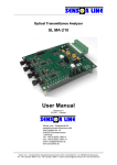
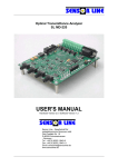
Optical Transmittance Analyzer
SL MA-310
User Manual
Revision 2.0
2012/07 – Plamper
Sensor Line - Gesellschaft für
optoelektronische Sensoren mbH
Carl-Poellath-Str. 19
D-86259 Schrobenhausen
- Germany Tel.: +49 (0) 8252 / 8943-0
Fax.:+49 (0) 8252 / 8943-11
Email: [email protected]
www.sensorline.de
Sensor Line - Gesellschaft für optoelektronische Sensoren mbH, Carl-Poellath-Str. 19, D-86529 Schrobenhausen
Tel.: +49 / (0) 8252 / 8943-0, Fax.: +49 / (0) 8252 / 8943-11, Email: [email protected], HP: www.sensorline.de
Table of Contents
1.
General........................................................................................................................ 3
1.1
1.2
1.3
2.
Function ................................................................................................................... 3
Features ................................................................................................................... 3
Dimensions............................................................................................................... 4
Connections................................................................................................................. 5
2.1
Electrical................................................................................................................... 5
2.1.1
2.1.2
2.1.3
2.1.4
2.2
3.
Optical ...................................................................................................................... 8
Output Circuitry............................................................................................................ 9
3.1
On-Board Pre-Wiring................................................................................................ 9
3.2
Wiring Examples .....................................................................................................12
3.2.1
3.2.2
3.2.3
3.2.4
4.
No Jumpers Installed ........................................................................................12
JP– Installed ...................................................................................................14
JP+ Installed .....................................................................................................14
Both Jumpers Installed......................................................................................15
Configuration ..............................................................................................................16
4.1
4.2
4.3
5.
On-Board Output Pre-Wiring ...................................................................................16
Selection Of Trigger Threshold................................................................................17
Selection Of Minimum Trigger Pulse Duration .........................................................18
Getting Started ...........................................................................................................19
5.1
5.2
6.
Power Supply (4-pin screw terminal or 4 pin header) ......................................... 5
Main Connector (12-pin pluggable screw terminal) ............................................ 6
Service Connector (14-pin header) .................................................................... 7
Measuring Pins .................................................................................................. 8
Installation ...............................................................................................................19
Test .........................................................................................................................19
Specifications .............................................................................................................20
-2-
1.
General
The SL MA-310 Optical Transmittance Analyzer (OTA) is an electronic interface that
operates three fiber optic load sensors. The unit serves as an interface between fiber optic
sensors and a processing unit on system level. It should be installed in a weather-proof road
side cabinet.
1.1
Function
The MA-310 responds to the optical sensor signal in a dynamic (AC-coupled) manner, i.e.
the electrical signal delivered when a load is applied to the sensor will decrease to zero as
the load continues to be applied. At a selectable threshold, a digital trigger signal is
generated for each channel. This signal can be forced to remain active for an selectable
length of time. Aside from these selections the interface does not require any further
adjustment.
The output (trigger) signals are transmitted via optocouplers which behave similar to relays,
allowing the use of a variety of output circuitry. In addition there is some output circuitry
implemented on the board which can by configured by means of jumpers, thus minimizing
the need for external wiring while still maintaining a maximum of output versatility.
Trigger activity and sensor failure are signaled by individual LEDs for every channel.
1.2
Features
• Dynamic three-channel interface for detection of light power changes caused by
activation of fiber-optic load sensors
• Optocoupler digital outputs
• Adjustable trigger threshold (0.3%, 0,5%, 1% and 1.5% relative light drop)
• Adjustable minimum trigger pulse duration (1ms, 22ms and 47ms)
• Trigger indication LED for each channel
• Error indication LED for each channel
• Reverse power protection
• Pre-wired output circuits configurable through jumper settings
• RoHS conform
-3-
0.25" (6.35 mm)
8" (203.2 mm)
7.5" (190.5 mm)
Dimensions
8.17" (207.5 mm)
1.3
Ø 0.15" (3.8 mm)
2.5" (63.5 mm)
0.25" (6.35 mm)
Not to scale!
3.5" (88.9 mm)
3.66" (93 mm)
Component Height:
Board Thickness:
11 mm (0.44“) maximum inside of board perimeter
15 mm (0.59”)
(connector plug)
0.17 mm (0.067”)
Component Lead Length: 2 mm (0.08”) maximum
Minimum clearance of mounting holes to adjacent traces: 2.5 mm (0.1”)
Note: Connector plug increases board width by 10 mm (0.4”), not including space for wire terminations.
-4-
2.
Connections
2.1
Electrical
2.1.1
Power Supply (4-pin screw terminal or 4 pin header)
0
1
2
3
Terminal/Pin #
0
1
2
3
0
1
2
3
Signal
Description
12...24 VDC
GND (AGND)
5...24 VDC
DGND
Board Supply Voltage
Board Analog Ground
Output Supply Voltage
Output Digital Ground
-5-
2.1.2
Main Connector (12-pin pluggable screw terminal)
Terminal #
Label
Signal
1
2
3
4
5
6
7 to 12
C (1)
(1) E
C (2)
(2) E
C (3)
(3) E
C1
E1
C2
E2
C3
E3
NC
-6-
Description
Collector Output of Channel 1
Emitter Output of Channel 1
Collector Output of Channel 2
Emitter Output of Channel 2
Collector Output of Channel 3
Emitter Output of Channel 3
Not connected
2.1.3
Service Connector (14-pin header)
Pin #
Signal
1
2
3
4
5
6
7
8
9
10
11
12
13
14
GND (AGND)
GND (AGND)
Vana1
Vmon1
Vtrg1
Vref1
Vana2
Vmon2
Vtrg2
Vref2
Vana3
Vmon3
Vtrg3
Vref3
Description
Board Analog Ground
Board Analog Ground
Analog Load Signal Channel 1
Monitor Signal Channel 1
Trigger Signal Channel 1
Reference Voltage Channel 1
Analog Load Signal Channel 2
Monitor Signal Channel 2
Trigger Signal Channel 2
Reference Voltage Channel 2
Analog Load Signal Channel 3
Monitor Signal Channel 3
Trigger Signal Channel 3
Reference Voltage Channel 3
-7-
2.1.4
2.2
Measuring Pins
Pin #
Label
Signal
Description
1
2
3
4
5
6
7
8
9
10
11
12
13
A3
M3
R3
T3
A2
M2
R2
T2
A1
M1
R1
T1
GND
Vana2
Vmon2
Vref2
Vtrg2
Vana2
Vmon2
Vref2
Vtrg2
Vana1
Vmon1
Vref1
Vtrg1
GND (AGND)
Analog Load Signal Channel 3
Monitor Signal Channel 3
Reference Voltage Channel 3
Trigger Signal Channel 3
Analog Load Signal Channel 2
Monitor Signal Channel 2
Reference Voltage Channel 2
Trigger Signal Channel 2
Analog Load Signal Channel 1
Monitor Signal Channel 1
Reference Voltage Channel 1
Trigger Signal Channel 1
Board Analog Ground
Optical
Channel 3
Channel 2
Channel 1
Transmitter Receiver Transmitter Receiver Transmitter Receiver
Six fibre-optic SMA-905 (FSMA) receptacles. The feeder fibres of each channel can be
connected in any order.
-8-
3.
3.1
Output Circuitry
On-Board Pre-Wiring
The MA-310 output circuitry is intended to facilitate interfacing of the unit to the host system
by minimizing the requirements for external wiring. In a majority of cases this can be accomplished using wires only without needing additional material such as extra terminal strips and
so on.
V+
1k
1k
JP+1
JP+2
C1
OC1
1k
C2
OC2
68V
68V
E1
C3
OC3
68V
E2
JP-1
JP+3
JP-2
E3
JP-3
V-
Fig. 1: MA-310 pre-wired output circuit
Fig. 1 shows the general arrangement: The signals are transmitted via optocouplers which
have an NPN phototransistors as their output stages. Collectors and emitters of these
phototransistors are directly connected to output terminals designated “C...” and “E...”.
In addition, there are two more terminals provided. The first one, “V+”, is connected via a
1kΩ resistor and a jumper “JP+...” to the collector of each optocoupler. The second one, “V–
“ is connected to its emitter via a jumper “JP–...“ only. The V+ and V– terminals are common
for all channels, whereas each channel has its own jumpers and resistors. This allows for a
variety of output configurations.
Please mind the Zener diodes which are omitted in the following drawings. They protect the
optocouplers not only against over-voltage but also – rather aggressively – against reverse
polarity. So whenever connecting a voltage source correct polarity should be observed for its
own sake.
-9-
V+
1k
JP+
C
OC
C
=ˆ
E
E
JP-
V-
Fig. 2: Both jumpers removed → Simple switch between Terminals C and E
When, according to Fig. 2, none of both jumpers of a channel is installed, collector and
emitter of the output transistor are only accessible via terminals C and E. The optocoupler
then acts as a simple switch, where of course polarity must be obeyed: current can only flow
into Terminal C and out of Terminal E.
V+
1k
JP+
C
C
OC
E
=ˆ
E
DGND
JPV-
DGND
Fig. 3: Jumper JP– installed, Terminal V– grounded
→ Terminal E grounded, Switch between Terminal C and ground
When Jumper JP– is installed and Terminal V– is grounded as shown in Fig. 3 the switch
also becomes grounded at its negative connection. In other words, the optocoupler then acts
as a switch between Terminal C and ground, plus, ground is available at Terminal E.
- 10 -
V+
DVCC
1k
JP+
1k
E
DGND
=ˆ
C
OC
DVCC
E
DGND
JP-
V-
Fig. 4: Jumper JP+ installed, Jumper JP– removed, Terminal V+ powered
→ Voltage source with 1kΩ series resistor at Terminal E
When Jumper JP+ is installed instead of JP– and Terminal V+ is connected to some voltage
DVCC according to Fig. 4 then a load can be switched via the optocoupler with a series
resistance of 1kΩ.
V+
DVCC
1k
JP+
DGND
1k
C
OC
=ˆ
E
DVCC
C
E
JP-
DGND
V-
DGND
Fig. 5: Both jumpers installed, Terminal V– grounded, Terminal V+ powered
→ Terminal E grounded, inverted voltage output at Terminal C
Installation of both jumpers, grounding of Terminal V– and connection of a voltage source to
Terminal V+ as shown in Fig. 5 establishes a true voltage output at Terminals C and E which
can drive floating inputs.
- 11 -
3.2
Wiring Examples
Configuration of the MA-310 output can be done with or without a separate output power
supply. If one is present it is recommendable to introduce a separate output ground as well.
This may reduce interference of the connected circuitry with the analog signal porcessing
significantly.
3.2.1
No Jumpers Installed (see Fig. 2)
It is obvious, that when neither of the jumpers is installed, it makes no sense to connect
anything to the V+ or V– terminals. The on-board pre-wiring is disabled in this case and the
optocoupler can be incorporated into any external circuitry. This causes some effort but
offers a maximum of versatility.
JP+
JP-
VCC
12...24V
GND
GND
JP+
GND
AGND
V+
V-
V-
C
JP-
Out
Fig. 6: External pull-up resistor with common
board and output supply
5...24V
C
Out
E
DGND
Fig. 7: External pull-up resistor with separate
board and output supply
VCC
12...24V
VCC
12...24V
GND
GND
GND
AGND
JP+
V+
V+
V-
VJP-
12...24V
V+
E
JP+
VCC
JP-
C
E
Out
C
5...24V
E
Out
DGND
Fig. 8: External pull-down resistor with
common board and output supply
Fig. 9: External pull-down resistor with
separate board and output supply
- 12 -
JP+
VCC
12...24V
GND
GND
JP+
VCC
12...24V
GND
AGND
V+
V+
R1
VJP-
V-
R2
JP-
C
E
R1
C
E
Out
Out
R2
Fig. 10: Non-inverted output level adjustment
with common board and output supply
DGND
Fig. 11: Non-inverted output level adjustment
with separate board and output supply
R2
⋅ (Vcc − 1V )
R1 + R2
≈ 0 (GND)
R2
⋅ (VR1 − 1V )
R1 + R2
≈ 0 (DGND)
VHigh ≈
VHigh ≈
VLow
VLow
JP+
5...24V
VCC
12...24V
VCC
12...24V
GND
GND
GND
AGND
JP+
V+
V+
TTL
VJP-
VJP-
C
E
Fig. 12: Driving a TTL gate with common
board and output supply
C
TTL
E
DGND
Fig. 13: Driving a TTL gate with separate
board and output supply
Note: Open TTL inputs behave as if connected to high-level. The above option applies to
such inputs only. Floating (e.g. CMOS) inputs must be driven according to Fig. 6 to 9.
JP+
VCC
12...24V
VCC
12...24V
GND
GND
GND
AGND
JP+
V+
V+
VJP-
VJP-
C
E
Fig. 14: Driving a LED or an optocoupler with
common board and output supply
C
5...24V
E
DGND
Fig. 15: Driving a LED or an optocoupler with
separate board and output supply
- 13 -
3.2.2
JP– Installed (see Fig. 3)
The circuits given below differ from the corresponding circuits in section 3.2.1 only in that the
ground wires are not connected directly to the optocoupler’s emitter but via the V– terminal
and the JP– jumper instead. However, since the V– terminal is common there is only one
wire needed to establish this connection for all channels.
JP+
VCC
12...24V
GND
GND
JP+
VCC
12...24V
GND
AGND
V+
V+
VJP-
C
JP-
Out
VCC
12...24V
GND
GND
Out
Fig. 17: External pull-up resistor with
separate board and output supply
JP+
VCC
12...24V
GND
AGND
V+
V+
V-
C
5...24V
Fig. 16: External pull-up resistor with
common board and output supply
JP-
DGND
E
E
JP+
V-
TTL
VJP-
C
DGND
C
E
E
TTL
Fig. 18: Driving a TTL gate with common
board and output supply
Fig. 19: Driving a TTL gate with separate
board and output supply
Note: Open TTL inputs behave as if connected to high-level. The above option applies to
such inputs only. Floating (e.g. CMOS) inputs must be driven according to Fig. 16 to 17.
3.2.3
JP+ Installed (see Fig. 4)
JP+
VCC
12...24V
GND
GND
JP+
VCC
12...24V
GND
AGND
V+
5...24V
V+
V-
VJP-
C
Out
Out
JP-
C
E
E
Fig. 20: Output level adjustment with
common board and output supply
DGND
Fig. 21: Output level adjustment with
separate board and output supply
R
⋅ (Vcc − 1V )
R + 1kΩ
≈ 0 (GND)
R
⋅ (V+ − 1V )
R + 1kΩ
≈ 0 (DGND)
VHigh ≈
VHigh ≈
VLow
VLow
- 14 -
JP+
VCC
12...24V
GND
GND
JP+
VCC
12...24V
GND
AGND
V+
5...24V
V+
V-
VJP-
JP-
C
C
E
E
Fig. 22: Driving a LED or an optocoupler with
common board and output supply
DGND
Fig. 23: Driving a LED or an optocoupler with
separate board and output supply
Note: The internal 1k resistor will deliver about 1 mA of current per volt of V+ to Terminal E.
The external resistor is only needed if this is too much. Also, with a separate output supply
the current can be adjusted via V+, thus also rendering the external resistor unnecessary.
3.2.4
Both Jumpers Installed (see Fig. 5)
Installing both jumpers allows for creating a voltage output (as opposed to a switch) without
the need of any external components.
JP+
VCC
12...24V
VCC
12...24V
GND
GND
GND
GND
JP+
V+
VJP-
C
JP-
Out
5...24V
V-
DGND
C
Out
E
E
Fig. 24: Simple voltage output with common
board and output supply
V+
Fig. 25: Simple voltage output with separate
board and output supply
- 15 -
4.
4.1
Configuration
JP+ Channel 1
On-Board Output Pre-Wiring
JP+ Channel 2
JP+ Channel 3
JP– Channel 1
JP– Channel 2
JP– Channel 3
The jumpers of the on-board output pre-wiring are accepted by a 2x8-pin header. With the
fibre-optic receptacles pointing up, this header is located immediately above the main output
connector.
The different output configurations described in Section 3 are established as shown below.
Jumpers
Outputs configured
according to
Fig. 2, Section 3.2.1
Fig. 3, Section 3.2.2
Fig. 4, Section 3.2.3
Fig. 5, Section 3.2.4
- 16 -
4.2
Selection Of Trigger Threshold
Channel 3
Channel 2
Channel 1
Trigger Threshold
With the fibre-optic receptacles pointing up, the headers for trigger threshold selection are
located above each channel’s measuring pins (see Section 2.1.4) and labeled THR1, THR2
and THR3.
The trigger threshold of each channel is determined by two jumpers placed as shown below.
Jumpers
Trigger Threshold
0.3%
0.5%
1.0%
1.5%
- 17 -
4.3
Selection Of Minimum Trigger Pulse Duration
Channel 3
Channel 2
Channel 1
Trigger Pulse Duration
With the fibre-optic receptacles pointing up, the headers for the selection of trigger pulse
duration are located to the left of each channel’s measuring pins (see Section 2.1.4) and
labeled PW1, PW2 and PW3.
The minimum trigger pulse duration of each channel is determined by one jumper placed as
shown below.
Jumper
Trigger Pulse min.
1 ms
22 ms
47 ms
- 18 -
5.
5.1
Getting Started
Installation
1) Fix the interface with screws and spacers. Take care that any vibrations or shocks will not
affect the board and in specific the fiber optic connectors.
2) Remove the safety caps from LED transmitter and photodetector.
3) Connect the sensor SMA connectors with transmitters and photodetectors of each channel. Fasten properly the sensor SMA connectors with transmitters and photo detectors in
order to obtain smallest attenuation, but avoid any violence; especially do not use pliers.
The connectors of transmitter and photodetector of each channel may be interchanged.
4) Connect the power supply (or power supplies) to the respective terminals.
5) Connect the signal output terminals to your system.
5.2
Test
1) Switch the power supply on.
2) Drive across the embedded sensors and monitor the trigger signals by watching the
Trigger LEDs.
3) Test the sensor failure signal of each channel by disconnecting one of its fiber
connectors. The respective Error LED must come on within few seconds.
- 19 -
6.
Specifications
Board Supply Voltage:
Board Supply Current (continuous):
Output Supply Voltage:
Rating of Optocouplers:
Trigger Thresholds:
Minimum Trigger Pulse Duration:
Sensor Attenuation for MA-310 RED:
Sensor Attenuation for MA-310 IR:
Speed Range:
Feeder Length:
Certification:
+12 to +24 VDC
< 400 mA
+ 5 to +24 VDC
60V / 25mA
0.3% / 0.5% / 1% / 1.5% of light transmittance drop
1 ms / 22 ms / 47 ms
3 – 23 dB (red transmitter)
3 – 33 dB (infrared transmitter)
1 to 250 km/h
up to 250 meters
RoHS
LED Risk Group:
RG 0 (safe) *
* According to DIN EN 62471. Please note: In spite of the official classification
SENSOR LINE recommends to avoid staring into the transmitter for longer
periods, regardless whether light is visible or not.
Important notice
All the information contained herein is believed to be accurate and reliable. However, SENSOR LINE
assumes no responsibility for its use or for any infringements of patents or other rights of third parties
that may result from its use. No license is granted by implication or otherwise under any patent rights of
SENSOR LINE GmbH.
SENSOR LINE GmbH SHALL NOT BE LIABLE FOR ANY SPECIAL, INCIDENTAL OR CONSEQUENTIAL DAMAGES RELATED TO THE USE OF THIS PRODUCT.
All rights reserved. Reproduction or adaptation of any part of this documentation without permission of
the copyright owner is unlawful.
- 20 -