1
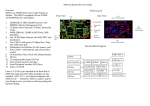
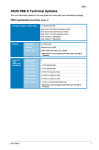
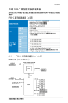
Revision History
Rev. 1.1
Revision
Date
Description
1.0
2006/10/17 First Release
1.1
2007/9/10
M-501 V3 hardware modification
Change the CN3 Pin 38 (PIO13) mapping from
CPU’s PC6 to PB22. Firmware is also changed
accordingly to ensure 100% software
compatibility with M-501 V2.
Reason: ATMEL technical note suggests not to
use PC6 as Digital I/O pin.
M501 Evaluation Kit User Guide
Linux 2.6 OS is pre-installed in the flash disk of M501
and many powerful utility programs are also included.
GNU C/C++ tool chain are shipped with M501 in CD.
Therefore, M501 is ready to drop in your design to
save your time in software porting and hardware
debug.
Artila uses M-501 to design Matrix-510/520. Please
refer to Matrix-510/520 user guide and if you are
interested in those design, please contact Artila.
Rear View
ARM9
FLASH
SDRAM
CN3
2mm 2x25 pins header
Φ 2mm (M2)
Mounting
Hole (M2)
Debug Port
CN1
2mm 2x14 pins header
JTAG Port
Φ 2mm (M2)
Φ 2mm (M2)
PHY LAN Transformer
CN2
2mm 2x25 pins header
Function Block Diagram
RJ45
Connector
SD Socket
SPI
Connector
SD
Interface
Power
+3.3VDC
USB Host
Interface
USB 2.0
Host
Connector
M501
SPI
Interface
8-bit Local
Bus
RS-232
Line Driver
External
Devices
I2C (TWI)
ARM920T ARM Thumb Processor with
200MIPS at 180MHz, Memory Management Unit
2. 16-KByte Data Cache and 16-KByte Instruction
Cache
3. 64MB SDRAM, 16MB Flash
4. One 10/100 Mbps Ethernet with MAC/PHY and
transformer
5. Two USB 2.0 full speed (12 Mbps) Host Ports
6. Multimedia Card Interface for SD memory card
7. Four UARTs with hardware and software flow
control
8. Two-wire Interface (I2C) for Real Time Clock
9. 32 Programmable Digital I/O Port
10. 8-bit external local bus interface
Front View
LAN
1.
M-501 Layout
UARTx4 (TTL)
Overview
M501 is an ARM9-based Linux ready System on
Module. The M501 is equipped with an ATMEL
AT91RM9200 SoC and features:
RTC
EEPROM
M501 Hardware Specifications
SoC: ATMEL AT91RM9200
CPU: ARM920T ARM Thumb Processor with Memory Management Unit (MMU)
Clock: 180MHz
SDRAM: 64MB
Flash: 16MB Intel StrataFlash or Equivalent
Ethernet: 10/100 Mbps with MAC/PHY and Transformer
PHY: DAVCOM DM9161
Transformer: 1.5 KV isolation
Signal: ETX0+, ETX0-, ERX0+, ERXUSB : USB 2.0 full speed (12Mbps) Host x2
Signal: UDataA+, UDataA-, UDataB+, UDataBUART: Four Universal Asynchronous Receiver and Transmitter
Data Bits: 5 to 9 bits
Parity: None, Even, Odd, Mark, Space
Stop: 1, 1.5, 2 bits
Baud Rate: Up to 921.6 Kbps
Flow Control: RTS/CTS, XON/XOFF, None
Multi-drop Mode with address generation and detection (COM1 only)
RS485 Driver Control Signal (COM1:RTS0)
Signal Level: CMOS/3.3V compatible
COM1: TXD0, RXD0, RTS0, CTS0 (RS485 Control: RTS0)
(Software configurable RS-232/422/485)
COM2: TXD1, RXD1, RTS1, CTS1, DCD1, DTR1, DSR1
( RS-232 with full modem control)
COM3: TXD2, RXD2, RTS2, CTS2
(RS-232 with hardware flow control)
COM4: TXD3, RXD3, RTS3, CTS3
(RS-232 with hardware flow control)
Inter-IC Bus: (I2C Bus)
Compatible with standard two-wire serial memory interface
Supported Devices: (Driver built-in)
Real Time Clock: Ricoh (RS5C372)
EEPROM: ATMEL AT24C16 and compatible
Signal: TWD, TWDK
I2S (internal IC Sound):
Transmitter: TSCK, TWS, TSD
Receiver: RSCK, RWS, RSD
Serial Peripheral Interface: (SPI)
Two chip Selects with external decoder
Three wires signals: MISO, MOSI and SPCK clock
Signal: MISO, MOSI, SPCK, CS1, CS2
Multimedia Card Interface
Compatible with SD memory card Specification 1.0
Signal: MCCDA, MCCK, MCDA0, MCDA1, MCDA2, MCDA3
Watchdog Timer: CPU built-in WDT and used by Linux Kernel
Programmable DIO
32 General Purpose IOs and can be programmable as digital input or output
Support interrupt function for digital inputs
Signal Level: CMOS/3.3V Compatible
Input:
Low level: -0.3V min
+0.8V max
High level: +2V min
+3.9V max
Output:
Low level: +0.4V max @0mA
+0.2V min @ 8mA
High level: +3.1V max @0mA
+2.9V min @ 8mA
Signal: PIO0 to PIO31
External Bus Interface:
8-bit data bus
Signal: D0~D7
8-bit address bus
Signal: A0~A7
4 Chip Selection
Signal: NCS3~NCS6
Signal Level: CMOS/3.3V
Predefine Pins:
Reset Button (CN2, pin#35, RST#1), input
Buzzer (CN2, pin#37, BUZR), output
System ready LED (CN2, pin#38, RDY_LED), output
LAN activity LED (CN3, pin#11, ACT_LED), output
Undefined Digital IO Pins (reserved)
CN1: pin#23, #24, #25, #26
CN3: pin#23, #24
Debug Port:
Serial Console: Tx/Rx
Signal: Tx share with RTS2
Rx share with CTS2
JTAG: For low level debug
Signal: NTRST, TDI, TMS, TCK, TDO
Power:
Input: 3.0 to 3.6VDC (3.3V nominal)
Consumption: 2.5W
M501 Software Specifications
OS: Linux 2.6.14
Boot Loader: U-Boot 1.1.2
File System: JFFS2, EXT2/EXT3, VFAT/FAT, NFS
Protocol Stacks:
IPV4, ICMP, ARP, DHCP, NTP, TCP, UDP, FTP, Telnet, HTTP, PPP,
PPPoE, CHAP, PAP, SMTP, SNMP V1/V3, SSL, SSH 1/2
Utilities:
Bash: Shell Command
Tinylogin: Login and user manager utility
Telnet: Telnet client program
Busybox: Linux utility collection
FTP: FTP client program
Daemon
pppd: Dial In/out over serial port and PPPoE
snmpd: SNMP agent program
telnetd: Telnet server program
inetd: TCP server program
ftpd: FTP server program
boa: Web server program
sshd: secured shell server
iptables: Firewall service manager
armd: Artila manager daemon
Tool Chain for Windows/Linux
GCC: C/C++ PC cross compiler
GLIBC: POSIX Library
Standard Device Drivers:
ttyS0: serial console port (AT91RM9200 debug port)
ttyS1~ttyS4: serial ports (AT91RM9200 UART0~UART3)
gpio: General Purpose I/O
mmc: SD/MMC:
rtc: Real Time Clock
sda: USB flash memory disk
ttyACM: USB Modem
ttyUSB: USB RS-232 adaptor
spi: spi bus
Default Setting
Default IP Address:192.168.2.127
Netmask: 255.255.255.0
ssh Login: root
Password: root
Telnet Login: guest
Password: guest
Terminal type: VT100
Network Configuration
To configure the IP address, Netmask and Gateway setting, please modify
/disk/etc/rc as following:
#Static IP
ifconfig eth0 192.168.2.127 netmask 255.255.255.0
For DHCP setting:
#DHCP
dhcpcd eth0 &
Wireless LAN Configuration
M-501 supports wireless LAN by using USB WLAN adaptor which uses Ralink RT2571
controller. Please refer to the website
http://ralink.rapla.net for the supporting list of the USB WLAN adaptor. To configure the
wireless LAN setting, please use command:
ifconfig wlan0 up
iwconfig wlan0 essid XXXX key YYYYYYYY mode MMMM
For infrastructure mode XXXX is the access point name and YYYYYYYY is the encryption key
and MMMM should be managed
For Ad-Hoc mode mode XXXX is the M-501 device name and YYYYYYYY is the encryption
key MMMM should be ad-hoc. To configure the IP address use command
dhcpcd wlan0 & or ifconfig wlan0 192.168.2.127 netmask 255.255.255.0
Install GNU Tool Chain
Find a PC with Linux 2.6.X Kernel installed and login as a root user then copy the arm-linux3.3.2.tar.gz to root directory \ of PC. Under \ directory type following command to install the
M-501 Tool Chain
#tar zxvf arm-linux-3.3.2.tar.gz
I/O Devices Control
M-501 uses standard I/O device control to access following devices:
1.
Ethernet: eth0
2.
Serial Ports: ttyS1, ttyS2, ttyS3,ttyS4
3.
Serial Console Port: ttyS0
4.
Real time clock: rtc
5.
USB Flash Disk: sda, sda1, sdb, sdb1
6.
SD memory Card: mmc0
7.
USB WLAN dongle: wlan0
8.
USB Serial Cable: ttyUSB0, ttyUSB1
9.
SPI bus: spi0, spi1
Remark: Remember to include the “matrix500.h” header file in your program. Please refer to the
example program included in the M-501 SDK CD to demo the RS-232/422/485 mode
configuration of serial port 1 configuration.
File System
Matrix 500 uses jffs2 file system for the built-in flash memory disk. The
directory are:
/disk
/home
/etc
Write data to these directories are saved to flash memory and will not be erased
after power off.
Mount External Disk
To mount the USB Flash Disk and SD memory card, use following commands
after the disk are installed properly. To mount USB disk
mount /mnt/sda or mount /mnt/sda1 or mount /mnt/sdb or mount /mnt/sdb1
To find out the device name of the USB disk, you can use
dmesg | grep sd
And to mount SD memory card
mount /mnt/mmc
Web Page Directory
The web pages are placed at /home/httpd and the boa.conf contains the boa web
server settings. The home page name should be index.html
Welcome Message
The welcome message “Artila” can be modified by editing the /etc/motd file.
Manager Utility Software
The Manager Utility software, manager.jar is a java program and is used to
discovered the Matrix 500 in the network if the IP address is forgotten. It can be
run at any OS where java run time is available. To install the java run time
platform at your computer, please visit http://java.sun.com and download the
Java 2 Standard Edition (J2SE). Once the Matrix 500 is found, you can click the
Telnet Console to configure the Matrix 500
Upload file to M-501
To upload the file to M-501, you can use FTP command in command line or Web
Browser such as Microsoft Internet Explorer. Type ftp://192.168.2.127 and
under the file menu, click log on option to login M-501. After login, you can see
the files system of M-501.
Compile and upload the C program
Use following command of the GNU cross compiler to compile the C program
#arm-linux-gcc –o hello hello.c
Then upload the hello to M-501. Remember to change the mode of the file
After upload to M-501 by
chmod +x hello
M501 Mechanical Dimension
Pin Assignment and Definition
Function
CPU
SoM
SoM
CPU
Function
CN1
(Addr Bus)
A0
1
2
D0
(Data Bus)
(Addr Bus)
A1
3
4
D1
(Data Bus)
(Addr Bus)
A2
5
6
D2
(Data Bus)
(Addr Bus)
A3
7
8
D3
(Data Bus)
(Addr Bus)
A4
9
10
D4
(Data Bus)
(Addr Bus)
A5
11
12
D5
(Data Bus)
(Addr Bus)
A6
13
14
D6
(Data Bus)
(Addr Bus)
A7
15
16
D7
(Data Bus)
NWE NWR0
17
18
NOE NRD
(Write Enable)
(Chip Select)
(Read Enable)
NCS3
CS3 19
20 CS4
NCS4
(Chip Select)
(Chip Select)
NCS5
CS5 21
22 CS6
NCS6
(Chip Select)
(N/A)
PA21
23
24
PA24
(N/A)
(N/A)
PB7
25
26
PB18
(N/A)
VCC3
27
28
GND
CN1
Pin Assignment and Definition
Function
CPU
SoM
SoM
CPU
Function
CN2
(COM2)
CTS2
1
2
DSR2
(COM2)
(COM2)
RTS2
3
4
RXD3
(COM3)
(COM3)
TXD3
5
6
CTS3
(COM3)
(COM3)
RTS3
7
8
TXD4
(COM4)
(COM4)
RXD4
9
10
RTS4
(COM4)
(COM4)
CTS4
11
12
PD22
(GPIO)
PD23
PC15
PD8
PD10
PD12
PD14
PD16
HDPB
HDMA
PD18
13
14 PIO16
16 PIO18
18 PIO20
20 PIO22
22 PIO24
24 PIO26
26 PIO28
28 UdataB30 UdataA+
32 PIO30
34
PC14
(GPIO)
(GPIO)
(GPIO)
(GPIO)
(GPIO)
(GPIO)
(GPIO)
(GPIO)
(USB B+)
(USB A-)
(GPIO)
(GPIO)
(Reset Btn)
(Buzzer)
(I2S transmitter)
(I2S transmitter)
(I2S receiver)
PD27
BTNRST#
PB6
PIO17
PIO19
PIO21
PIO23
PIO25
PIO27
UdataB+
UdataAPIO29
15
17
19
21
23
25
27
29
31
PIO31 33
PD7
PD9
PD11
PD13
PD15
PD17
HDMB
HDPA
PD26
VCC3 PWROK
(GPIO)
(GPIO)
(GPIO)
(GPIO)
(GPIO)
(GPIO)
(USB B-)
(USB A+)
(GPIO)
(System Reset)
35
36
NTRST
37
38
PD6
(System Ready LED)
40 TSCK
42 RSD
44 RWS
46
TK2
RD2
RF2
GND
(I2S transmitter)
(I2S receiver)
(I2S receiver)
TF2
TD2
RK2
GND
TWS 39
TSD 41
RSCK 43
45
GND
47
48
GND
VCC3
49
50
VCC3
CN2
(JTAG Reset)
Pin Assignment and Definition
Function
CPU
SoM
SoM
CPU
Function
CN3
VCC3
1
2
VCC3
GND
3
4
GND
GND
5
6
GND
(LAN)
ERX0-
7
8
ERX0+
(LAN)
(LAN)
ETX0-
9
10
ETX0+
(LAN)
(LAN LED)
ACTLED# 11
12
MISO
(SPI)
(SPI)
MOSI
13
14
SPCK
(SPI)
(SPI)
NPCS0
15
16
NPCS1
(SPI)
(SD)
MCCK
17
18
MCCDA
(SD)
(SD)
MCDA0
19
20
MCDA1
(SD)
(SD)
MCDA2
21
22
MCDA3
(SD)
(N/A)
PD19
23
24
PD20
(N/A)
(I2C)
25
26
27
29
31
33
35
37
39
41
28
30
32
34
36
38
40
42
TWCK
PB2
PB9
PB11
PC1
PC3
PB22
PB29
PD25
(I2C)
(GPIO)
(GPIO)
(GPIO)
(GPIO)
(GPIO)
(GPIO)
(GPIO)
(GPIO)
TWD
PA19
PB8
PB10
PC0
PC2
PC5
PB28
PD24
(COM1)
TXD1
43
44
RXD1
(COM1)
(COM1)
CTS1
45
46
RTS1
(COM1)
(COM2)
DTR2
47
48
TXD2
(COM2)
(COM2)
RXD2
49
50
DCD2
(COM2)
PIO1
PIO4
PIO6
PIO8
PIO10
PIO12
PIO14
PIO0
CN3
PIO3
PIO5
PIO7
PIO9
PIO11
PIO13
PIO15
PIO2
(GPIO)
(GPIO)
(GPIO)
(GPIO)
(GPIO)
(GPIO)
(GPIO)
(GPIO)
M501 Evaluation Board Layout
Reset Button
GPIO 0~15
Power +9~40VDC
LAN 1
USB 2.0 Host
DIP Switches
CN2
Power LED
Ready LED
LAN Link/Act
CN1
GPIO 16~31
CN8
CN3
LED
COM1 ~4
CN7
COM1
RS-232
RS-422
RS-485
COM2
RS-232
With
RTS
CTS
COM3
RS-232
With
RTS
CTS
COM4
RS-232
With
RTS
CTS
Enable Serial Console Port
Step 1: M-501 serial console port (ttyS0) shares three data pins with serial
port P3 (RS-232 port ttyS3).
ttyS0. Tx <=> ttyS3. RTS
ttyS0. Rx
<=> ttyS3. CTS
ttyS0.GND <=> ttyS3. GND
Connect the Console cable to Port 3 and the serial port of your computer
Step 4: Now you can type “A” to enable the serial console
function. Once you see the console is enabled as follow,
Press “q” to return to main menu of console. Then please
type ”R” to reboot the system.
Console Port via P3 Connector
Step 2: Once the serial console (ttyS0) are connected correctly to your PC,
you need to use a terminal software such as hyper terminal of Microsoft
and the serial port setting as 115200,N,8,1 and no flow control. Terminal
type is VT100.
Step 3: Power on M-501 then you will see the message from your terminal
software as follow:
Once “Starting Matrix 500” appears, please keep typing “@” to trigger the
serial load program. Then you will see the Artila loader menu appear. If
you miss the trigger procedure, please reset the M501 and repeat step 3
again.
Step 5: Once you complete system debug, please remember to disable
the serial console using the Toggle Console item by typing “A”..
Pin Assignment of Connectors
LAN 1 and LAN2
COM Port
CN8 Local Bus Connector
1.
2.
A0
A1
A2
GPIO Port 0~15 and GPIO Port 16~31
DIO0
DIO2
3
1
TxD
A6
RxD
A7
VCC3
NWE_NWR0
GND
NCS3
DIO1
JP1 of M501
Boot Mode Selection Jumper
PB7
VCC3
1
2
3
4
5
6
7
8
9
10
11
12
13
14
15
16
17
18
19
20
21
22
23
24
25
26
27
28
CN7 (SPI) Pin Assignment
1
MISO (Master In Slave Out)
2
MOSI (Master Out Slave In)
3
SPCK (SPI Serial Clock)
4
NPCS0 (SPI Chip Select 0)
5
NPCS1 (SPI Chip Select 1)
DIO17
4
2
DIO19
6
DIO23
DIO21
PA21
1-2: Internal ROM
2-3: External Flash (Default)
1
2
3
DIO16
DIO18
DIO3
4
2
PC11/NCS5
3
1
DIO6
DIO4
6
DIO20
DIO8
9
7
5
DIO22
DIO7
DIO5
8
10
DIO9
DIO24
9
7
5
8
10
DIO26
1
2
3
4
A4
A5
CN4 JTAG Connector
DIO25
DIO10
DIO12
13
11
12
14
DIO13
DIO11
DIO28
13
11
12
14
DIO29
DIO27
GND
DIO14
15
16
DIO15
15
16
DIO31
19
20
17
GND
DIO30
17
19
20
+3.3V
GND
18
+5V
+3.3V
GND
18
+5V
JP2 Serial Console Port
A3
1x14 Pin Header Pitch 2.54mm
CN8 directly connect to CN1 of M501
VCC3 (3.3V)
1
2
NTRST
GND
3
4
TDI
TDO
5
6
TMS
VCC3_PWROK
7
8
TCK
D0
D1
D2
D3
D4
D5
D6
D7
NOE_NRD
PC10/NCS4
PC12/NCS6
PA24
PB18
GND